JP6488590B2 - Conductive member, solar watch, solar cell module, electronic device - Google Patents
Conductive member, solar watch, solar cell module, electronic device Download PDFInfo
- Publication number
- JP6488590B2 JP6488590B2 JP2014171261A JP2014171261A JP6488590B2 JP 6488590 B2 JP6488590 B2 JP 6488590B2 JP 2014171261 A JP2014171261 A JP 2014171261A JP 2014171261 A JP2014171261 A JP 2014171261A JP 6488590 B2 JP6488590 B2 JP 6488590B2
- Authority
- JP
- Japan
- Prior art keywords
- solar cell
- battery
- piece
- conductive layer
- notch
- Prior art date
- Legal status (The legal status is an assumption and is not a legal conclusion. Google has not performed a legal analysis and makes no representation as to the accuracy of the status listed.)
- Active
Links
- 239000000463 material Substances 0.000 claims description 51
- 239000000758 substrate Substances 0.000 claims description 48
- 230000000149 penetrating effect Effects 0.000 claims description 2
- 210000004027 cell Anatomy 0.000 description 160
- 239000010408 film Substances 0.000 description 63
- 229910021417 amorphous silicon Inorganic materials 0.000 description 13
- XLOMVQKBTHCTTD-UHFFFAOYSA-N Zinc monoxide Chemical compound [Zn]=O XLOMVQKBTHCTTD-UHFFFAOYSA-N 0.000 description 12
- 238000010248 power generation Methods 0.000 description 10
- LEVVHYCKPQWKOP-UHFFFAOYSA-N [Si].[Ge] Chemical compound [Si].[Ge] LEVVHYCKPQWKOP-UHFFFAOYSA-N 0.000 description 9
- 238000010586 diagram Methods 0.000 description 9
- 239000004020 conductor Substances 0.000 description 7
- 238000005452 bending Methods 0.000 description 6
- 239000011787 zinc oxide Substances 0.000 description 6
- 229910052782 aluminium Inorganic materials 0.000 description 4
- XAGFODPZIPBFFR-UHFFFAOYSA-N aluminium Chemical compound [Al] XAGFODPZIPBFFR-UHFFFAOYSA-N 0.000 description 4
- 229910052751 metal Inorganic materials 0.000 description 3
- 239000002184 metal Substances 0.000 description 3
- 239000011347 resin Substances 0.000 description 3
- 229920005989 resin Polymers 0.000 description 3
- RYGMFSIKBFXOCR-UHFFFAOYSA-N Copper Chemical compound [Cu] RYGMFSIKBFXOCR-UHFFFAOYSA-N 0.000 description 2
- 239000011889 copper foil Substances 0.000 description 2
- 229910052732 germanium Inorganic materials 0.000 description 2
- GNPVGFCGXDBREM-UHFFFAOYSA-N germanium atom Chemical compound [Ge] GNPVGFCGXDBREM-UHFFFAOYSA-N 0.000 description 2
- 230000009467 reduction Effects 0.000 description 2
- 229910000577 Silicon-germanium Inorganic materials 0.000 description 1
- 238000010521 absorption reaction Methods 0.000 description 1
- 230000008901 benefit Effects 0.000 description 1
- 210000005056 cell body Anatomy 0.000 description 1
- 230000008859 change Effects 0.000 description 1
- 238000005553 drilling Methods 0.000 description 1
- 239000011521 glass Substances 0.000 description 1
- 230000036541 health Effects 0.000 description 1
- 230000001771 impaired effect Effects 0.000 description 1
- 238000009413 insulation Methods 0.000 description 1
- 239000007769 metal material Substances 0.000 description 1
- 238000000034 method Methods 0.000 description 1
- 238000012856 packing Methods 0.000 description 1
- 238000005192 partition Methods 0.000 description 1
- 239000000088 plastic resin Substances 0.000 description 1
- 230000008569 process Effects 0.000 description 1
- 229910001220 stainless steel Inorganic materials 0.000 description 1
- 239000010935 stainless steel Substances 0.000 description 1
- 239000010409 thin film Substances 0.000 description 1
- 238000002834 transmittance Methods 0.000 description 1
- 210000000707 wrist Anatomy 0.000 description 1
Images


Classifications
-
- G—PHYSICS
- G04—HOROLOGY
- G04C—ELECTROMECHANICAL CLOCKS OR WATCHES
- G04C10/00—Arrangements of electric power supplies in time pieces
- G04C10/02—Arrangements of electric power supplies in time pieces the power supply being a radioactive or photovoltaic source
-
- H—ELECTRICITY
- H01—ELECTRIC ELEMENTS
- H01L—SEMICONDUCTOR DEVICES NOT COVERED BY CLASS H10
- H01L31/00—Semiconductor devices sensitive to infrared radiation, light, electromagnetic radiation of shorter wavelength or corpuscular radiation and specially adapted either for the conversion of the energy of such radiation into electrical energy or for the control of electrical energy by such radiation; Processes or apparatus specially adapted for the manufacture or treatment thereof or of parts thereof; Details thereof
- H01L31/02—Details
- H01L31/02002—Arrangements for conducting electric current to or from the device in operations
- H01L31/02005—Arrangements for conducting electric current to or from the device in operations for device characterised by at least one potential jump barrier or surface barrier
- H01L31/02008—Arrangements for conducting electric current to or from the device in operations for device characterised by at least one potential jump barrier or surface barrier for solar cells or solar cell modules
-
- Y—GENERAL TAGGING OF NEW TECHNOLOGICAL DEVELOPMENTS; GENERAL TAGGING OF CROSS-SECTIONAL TECHNOLOGIES SPANNING OVER SEVERAL SECTIONS OF THE IPC; TECHNICAL SUBJECTS COVERED BY FORMER USPC CROSS-REFERENCE ART COLLECTIONS [XRACs] AND DIGESTS
- Y02—TECHNOLOGIES OR APPLICATIONS FOR MITIGATION OR ADAPTATION AGAINST CLIMATE CHANGE
- Y02E—REDUCTION OF GREENHOUSE GAS [GHG] EMISSIONS, RELATED TO ENERGY GENERATION, TRANSMISSION OR DISTRIBUTION
- Y02E10/00—Energy generation through renewable energy sources
- Y02E10/50—Photovoltaic [PV] energy
Description
本発明は、導通部材、ソーラーウォッチ、太陽電池モジュール、電子機器に関する。 The present invention relates to a conductive member, a solar watch, a solar cell module, and an electronic device.
従来、モバイル用太陽電池の電極接点の実装については、視認側に設けられる透明電極と反対面側に設けられる対向電極の接点を同一面上に導出するために様々な形状が工夫されている。例えば、下記特許文献1に開示の発明では、基材そのものにスルーホールを設けている。また、モバイル用太陽電池においては発電時の電圧を向上させることが重要である。そこで、従来、発電電圧を高めるべく、金属Inを用いて複数の太陽電池同士を直列接続した構造が知られている(例えば、下記特許文献2参照)。
Conventionally, regarding the mounting of electrode contacts of a mobile solar cell, various shapes have been devised in order to lead out the contact of the counter electrode provided on the opposite side to the transparent electrode provided on the viewing side on the same surface. For example, in the invention disclosed in the following
しかしながら、上記特許文献1に開示の発明は、穴あけ加工、端部絶縁処理、及び導電性ペーストによる穴埋め処理が必要となるため、工程が複雑であることから歩留まりの低下による信頼性の低下、あるいはコスト上昇といった問題があった。また、上記特許文献2に開示の発明では、金属Inによって十分な接続強度を保とうとした場合、膜厚が非常に薄い発電層が破壊されることで導通不良が生じるといった問題があった。
However, since the invention disclosed in
本発明は、上述の課題の少なくとも一部を解決するためになされたものであり、以下の形態または適用例として実現することが可能である。また、低コストで且つ高い導通(接続)信頼性を得ることができる導通部材及びソーラーウォッチを提供することを目的の一つとする。 SUMMARY An advantage of some aspects of the invention is to solve at least a part of the problems described above, and the invention can be implemented as the following forms or application examples. Another object is to provide a conductive member and a solar watch that can be obtained at low cost and have high continuity (connection) reliability.
[適用例]本適用例に係る導通部材は、隣り合って配置されると共に、表裏両面に電極を有する第1電池及び第2電池を電気的に接続させる導通部材であって、可撓性の基材と、前記基材の一方の面に設けられた第1導電層と、前記基材の他方の面に設けられた第2導電層と、を備え、前記基材を折り曲げて、前記第1導電層を前記第1電池の表面側電極に接続させ、前記第2導電層を前記第1電極の裏面側電極と前記第2電池の表面側電極とに接続させることを特徴とする。 [Application Example] The conduction member according to this application example is a conduction member that is arranged adjacent to each other and electrically connects the first battery and the second battery having electrodes on both front and back surfaces, and is flexible. A base material, a first conductive layer provided on one surface of the base material, and a second conductive layer provided on the other surface of the base material, bending the base material, One conductive layer is connected to a surface side electrode of the first battery, and the second conductive layer is connected to a back side electrode of the first electrode and a front side electrode of the second battery.
本適用例によれば、第1電池の表面側電極と第2電池の裏面側電極との電気的な接続における配線層の引き回しと、2つの電池の直列接続とを1つの導通部材によって実現することができる。よって、部品点数の削減、あるいは接続作業に伴う工数の削減を図ることができ、結果的にコスト低減を図ることができる。また、可撓性の基材を主体に構成されるため、第1導電層、第2導電層の引き回しが簡便且つ確実に行われて、第1電池及び第2電池間における接続信頼性を向上させることができる。 According to this application example, the wiring layer in the electrical connection between the front-side electrode of the first battery and the back-side electrode of the second battery and the series connection of the two batteries are realized by one conductive member. be able to. Therefore, it is possible to reduce the number of parts or man-hours associated with the connection work, and as a result, cost can be reduced. Moreover, since it is mainly composed of a flexible base material, the first conductive layer and the second conductive layer can be easily and reliably routed to improve the connection reliability between the first battery and the second battery. Can be made.
上記適用例に記載の導通部材において、前記第1電池には第1の切欠が設けられ、前記第2電池には第2の切欠が設けられており、前記基材は、本体部と、前記本体部から互いに異なる方向に延出した第1延出部及び第2延出部とを有し、前記基材の前記第1延出部は、前記第1の切欠で折り曲げられて前記第1電池の表面側に引き出され、前記第1導電層の前記第1延出部に設けられた部分が前記第1電池の表面側電極に接続され、前記基材の前記第2延出部は、前記第2の切欠で折り曲げられて前記第2電池の表面側に引き出され、前記第2導電層の前記第2延出部に設けられた部分が前記第2電池の表面側電極に接続され、前記基材の前記本体部は、前記第1の切欠と前記第2の切欠との間で、前記第1電池及び前記第2電池の裏面側に位置し、前記第2導電層の前記本体部に設けられた部分が前記第1電池の裏面側電極に接続されることを特徴とする。
この構成によれば、隣り合う第1電池と第2電池の隙間から導通部材を引き出すことが困難であっても、それぞれの電池に設けられた切欠から延出部を引き出して、第1電池及び第2電池のそれぞれの表面側電極に接続させることができる。言い換えれば、第1電池と第2電池とを近づけて配置しても電気的に直列接続が可能となる。
In the conductive member according to the application example, the first battery is provided with a first notch, the second battery is provided with a second notch, and the base material includes a main body portion, the A first extension part and a second extension part extending in different directions from the main body part, and the first extension part of the base material is bent at the first notch and the first extension part. A portion that is drawn to the surface side of the battery and is provided on the first extension portion of the first conductive layer is connected to a surface side electrode of the first battery, and the second extension portion of the base is Bent at the second notch and pulled out to the surface side of the second battery, and the portion of the second conductive layer provided on the second extending portion is connected to the surface side electrode of the second battery; The main body portion of the base is between the first notch and the second notch, and the back side of the first battery and the second battery. Position, and wherein the portion provided in the main body portion of the second conductive layer is connected to the back surface side electrode of the first battery.
According to this configuration, even if it is difficult to pull out the conducting member from the gap between the adjacent first battery and the second battery, the extension portion is pulled out from the notch provided in each battery, and the first battery and It can connect with each surface side electrode of a 2nd battery. In other words, even if the first battery and the second battery are arranged close to each other, they can be electrically connected in series.
上記適用例に記載の導通部材において、前記第1導電層及び前記第2導電層の少なくとも一方が、前記基材に形成されたスルーホールを介して前記第1電池の表面側電極及び/または前記第2電池の表面側電極に接続されるとしてもよい。
この構成によれば、第1導電層及び第2導電層の少なくとも一方について、表面側電極への接続部分を折り曲げることなく電気的な接続を行うことが可能な付加価値の高い導通部材を提供できる。
In the conductive member according to the application example, at least one of the first conductive layer and the second conductive layer is a surface-side electrode of the first battery and / or the through-hole formed in the base material. It may be connected to the surface side electrode of the second battery.
According to this configuration, it is possible to provide a high-value-added conductive member that can electrically connect at least one of the first conductive layer and the second conductive layer without bending the connection portion to the surface-side electrode. .
上記適用例に記載の導通部材において、前記第1導電層及び前記第2導電層は、少なくとも前記基材が折り曲げられる部分において、絶縁層で覆われていることが好ましい。
この構成によれば、第1電池または第2電池の端面に対し、第1導電層または第2導電層が接触して生ずる短絡を、絶縁層により回避することができる。
In the conductive member according to the application example, it is preferable that the first conductive layer and the second conductive layer are covered with an insulating layer at least in a portion where the base material is bent.
According to this configuration, a short circuit caused by the contact of the first conductive layer or the second conductive layer with the end surface of the first battery or the second battery can be avoided by the insulating layer.
上記適用例に記載の導通部材において、前記第1電池及び前記第2電池が太陽電池片であるとしてもよい。
この構成によれば、2つの太陽電池片における表裏面の電極間の直列接続を簡便且つ確実に可能とする導電部材を提供することができる。
In the conducting member according to the application example, the first battery and the second battery may be solar battery pieces.
According to this structure, the electrically-conductive member which enables the serial connection between the electrodes of the front and back surfaces in two solar cell pieces simply and reliably can be provided.
[適用例]本適用例に係るソーラーウォッチは、一対の太陽電池片と、前記一対の太陽電池片を直列に接続させる上記適用例に記載の導通部材とを含む太陽電池モジュールと、前記太陽電池モジュールからの電力により駆動する駆動部と、を備えることを特徴とする。
本適用例によれば、一対の太陽電池片が導通部材により高い信頼性で直列的に接続された太陽電池モジュールを備えるので、1つの太陽電池片を用いる場合に比べて高い駆動電圧を得ることができる。よって、安定した電力により駆動可能な信頼性の高いソーラーウォッチを低コストで提供することができる。
[Application Example] A solar watch according to this application example includes a solar cell module including a pair of solar cell pieces and the conductive member according to the application example in which the pair of solar cell pieces are connected in series, and the solar cell. And a drive unit that is driven by electric power from the module.
According to this application example, since the pair of solar cell pieces includes the solar cell module connected in series with high reliability by the conductive member, a high driving voltage is obtained as compared with the case of using one solar cell piece. Can do. Therefore, a highly reliable solar watch that can be driven by stable electric power can be provided at low cost.
上記適用例に記載のソーラーウォッチにおいて、前記導通部材は、前記一対の太陽電池片のそれぞれに形成された切欠を介して前記一対の太陽電池片の両面に引き出された状態に配置されていることを特徴とする。
この構成によれば、導通部材により太陽電池片の両面側において簡便且つ確実に接続を取る構造を実現することができる。言い換えれば、太陽電池モジュールからの出力を一対の太陽電池片の裏面側から得られる構造を実現できる。ゆえに、太陽電池モジュールの表面と裏面とから出力を取り出す構造に比べて薄型で簡素な構造とすることができる。
In the solar watch according to the application example, the conductive member is arranged in a state of being drawn out on both surfaces of the pair of solar cell pieces through a notch formed in each of the pair of solar cell pieces. It is characterized by.
According to this configuration, it is possible to realize a structure that can easily and reliably connect the both sides of the solar cell piece with the conducting member. In other words, a structure in which the output from the solar cell module can be obtained from the back side of the pair of solar cell pieces can be realized. Therefore, compared with the structure which takes out an output from the surface and back surface of a solar cell module, it can be set as a thin and simple structure.
上記適用例に記載のソーラーウォッチにおいて、二次電池を含む電源装置を備え、前記一対の太陽電池片のうちの一方の太陽電池片の表面側電極に接続された前記第1導電層と、前記一対の太陽電池片のうち他方の太陽電池片の裏面側電極とが、前記電源装置に接続され、前記二次電池を充電可能となっていることを特徴とする。
この構成によれば、一対の太陽電池片により発電した電力を二次電池に蓄えることが可能であることから、一対の太陽電池片から電力が得られ難い夜間などの暗所であっても正確に時を刻むことができるソーラーウォッチを提供できる。
In the solar watch according to the application example, the first conductive layer including a power supply device including a secondary battery, connected to a surface side electrode of one of the pair of solar cell pieces, and the Of the pair of solar cell pieces, the back surface side electrode of the other solar cell piece is connected to the power supply device and is capable of charging the secondary battery.
According to this configuration, since the power generated by the pair of solar cell pieces can be stored in the secondary battery, it is accurate even in a dark place such as at night when it is difficult to obtain power from the pair of solar cell pieces. A solar watch that can keep track of time.
[適用例]本適用例に係る太陽電池モジュールは、隣り合って配置されると共に、表裏両面に電極を有する第1太陽電池片及び第2太陽電池片と、可撓性の基材と、前記基材の一方の面に設けられた第1導電層と、前記基材の他方の面に設けられた第2導電層と、を含む導通部材と、を備え、前記基材が折り曲げられて、前記第1導電層は前記第1太陽電池片の表面側電極に接続され、前記第2導電層は前記第1太陽電池片の裏面側電極と前記第2太陽電池片の表面側電極とに接続されていることを特徴とする。 [Application Example] A solar cell module according to this application example is arranged adjacent to each other, and has first and second solar cell pieces having electrodes on both front and back surfaces, a flexible base material, A conductive member including a first conductive layer provided on one surface of the base material and a second conductive layer provided on the other surface of the base material, and the base material is bent, The first conductive layer is connected to the front side electrode of the first solar cell piece, and the second conductive layer is connected to the back side electrode of the first solar cell piece and the front side electrode of the second solar cell piece. It is characterized by being.
本適用例によれば、2つの太陽電池片が導通部材により直列に接続されているので、1つの太陽電池片を用いる場合に比べて高い駆動電圧を得ることが可能であると共に、高い接続信頼性を有する太陽電池モジュールを提供することができる。 According to this application example, since the two solar cell pieces are connected in series by the conductive member, it is possible to obtain a higher driving voltage than in the case of using one solar cell piece, and high connection reliability. A solar cell module having the characteristics can be provided.
上記適用例に記載の太陽電池モジュールにおいて、前記第1太陽電池片に設けられた第1の切欠と、前記第2太陽電池片に設けられた第2の切欠と、を備え、前記基材は、本体部と、前記本体部から互いに異なる方向に延出した第1延出部及び第2延出部とを有し、前記基材の前記第1延出部は、前記第1の切欠で折り曲げられて前記第1電池の表面側に引き出され、前記第1導電層の前記第1延出部に設けられた部分が前記第1電池の表面側電極に接続され、前記基材の前記第2延出部は、前記第2の切欠で折り曲げられて前記第2電池の表面側に引き出され、前記第2導電層の前記第1延出部に設けられた部分が前記第2電池の表面側電極に接続され、前記基材の前記本体部は、前記第1の切欠と前記第2の切欠との間で、前記第1電池及び前記第2電池の裏面側に位置し、前記第2導電層の前記本体部に設けられた部分が前記第1電池の裏面側電極に接続されていることを特徴とする。 In the solar cell module according to the application example described above, the solar cell module includes: a first notch provided in the first solar cell piece; and a second notch provided in the second solar cell piece, wherein the base material is And a first extending portion and a second extending portion that extend in different directions from the main body portion, and the first extending portion of the base material is the first notch. The bent portion is pulled out to the surface side of the first battery, and the portion of the first conductive layer provided on the first extending portion is connected to the surface-side electrode of the first battery, The second extending portion is bent at the second notch and pulled out to the surface side of the second battery, and a portion provided on the first extending portion of the second conductive layer is a surface of the second battery. The first battery is connected to a side electrode, and the main body portion of the substrate is between the first notch and the second notch. Located on the back side of the fine the second battery, wherein the portion provided in the main body portion of the second conductive layer is connected to the back surface side electrode of the first battery.
この構成によれば、隣り合う第1太陽電池片と第2太陽電池片の隙間から導通部材を引き出すことが困難であっても、それぞれの太陽電池片に設けられた切欠から延出部を引き出して、第1太陽電極片及び第2太陽電池片のそれぞれの表面側電極に接続させることができる。言い換えれば、第1太陽電池片と第2太陽電池片とを近づけて配置しても電気的に直列接続が可能な太陽電池モジュールを提供することができる。 According to this configuration, even if it is difficult to pull out the conductive member from the gap between the adjacent first solar cell piece and the second solar cell piece, the extension portion is pulled out from the notch provided in each solar cell piece. And it can be connected to each surface side electrode of a 1st solar electrode piece and a 2nd solar cell piece. In other words, a solar cell module that can be electrically connected in series even when the first solar cell piece and the second solar cell piece are arranged close to each other can be provided.
上記適用例に記載の太陽電池モジュールにおいて、前記第1の切欠と前記第2の切欠とは、隣り合う前記第1太陽電池片と前記第2太陽電池片との隙間を挟んで配置されていることを特徴とする。
この構成によれば、導通部材による第1太陽電池片と第2太陽電池片との接続距離を比較的に短くすることができる。つまり、導通部材の配線抵抗による電力の損出を小さくすることができる。
In the solar cell module according to the application example, the first notch and the second notch are arranged with a gap between the adjacent first solar cell piece and the second solar cell piece interposed therebetween. It is characterized by that.
According to this configuration, the connection distance between the first solar cell piece and the second solar cell piece by the conductive member can be made relatively short. That is, power loss due to the wiring resistance of the conductive member can be reduced.
上記適用例に記載の太陽電池モジュールにおいて、前記第1の切欠及び前記第2の切欠の少なくとも一方は、前記第1太陽電池片及び/または前記第2太陽電池片を貫通する孔であることを特徴とする。
この構成によれば、第1延出部及び/または第2延出部は、切欠としての孔から引き出されるので、引き出し位置がずれ難く、外力によって接続信頼性が損なわれることを低減することができる。
In the solar cell module according to the application example, at least one of the first notch and the second notch is a hole penetrating the first solar cell piece and / or the second solar cell piece. Features.
According to this configuration, since the first extension part and / or the second extension part are drawn out from the hole as the notch, the drawing position is difficult to shift, and it is possible to reduce the loss of connection reliability due to external force. it can.
上記適用例に記載の太陽電池モジュールにおいて、前記第2の切欠は、隣り合う前記第1太陽電池片と前記第2太陽電池片との前記隙間の一部を成していることを特徴とする。
この構成によれば、隙間に面する第2太陽電池片に第2の切欠を設けることで、当該隙間を利用して、第1太陽電池片と第2太陽電池片とを導通部材で直列接続できることから、第1太陽電池片と第2太陽電池片との接続距離をさらに短くすることができる。
In the solar cell module according to the application example, the second notch forms a part of the gap between the adjacent first solar cell piece and the second solar cell piece. .
According to this configuration, by providing the second notch in the second solar cell piece facing the gap, the first solar cell piece and the second solar cell piece are connected in series by the conductive member using the gap. Since it can do, the connection distance of a 1st solar cell piece and a 2nd solar cell piece can be shortened further.
上記適用例に記載の太陽電池モジュールにおいて、前記第1延出部及び前記第2延出部のぞれぞれは、第1分岐端部及び第2分岐端部を有し、前記第1延出部の前記第1分岐端部が前記第1の切欠から前記第1電池の表面側に引き出され、前記第1導電層の前記第1分岐端部に設けられた部分が前記第1電池の表面側電極に接続され、前記第2延出部の前記第1分岐端部が前記第2の切欠から前記第2電池の表面側に引き出され、前記第2導電層の前記第1分岐端部に設けられた部分が前記第2電池の表面側電極に接続され、前記第1延出部及び前記第2延出部の前記第2分岐端部は、隣り合う前記第1太陽電池片及び前記第2太陽電池片の裏側に配置されていることを特徴とする。
この構成によれば、第1延出部及び第2延出部のそれぞれの端部を切欠から引き出す場合に比べて、第1分岐端部が表面側に引き出され、第2分岐端部が裏面側に配置されるので、第1分岐端部と第2分岐端部とにより太陽電池片を挟んで支持することができる。つまり、第1太陽電池片及び第2太陽電池片のより強固な電気的接続構造を実現できる。
In the solar cell module according to the application example, each of the first extension part and the second extension part includes a first branch end part and a second branch end part, and the first extension part is provided. The first branch end portion of the protruding portion is drawn from the first notch to the surface side of the first battery, and the portion provided on the first branch end portion of the first conductive layer is the first battery end portion. The first branch end of the second conductive layer is connected to the surface side electrode, and the first branch end of the second extension is drawn out from the second notch to the surface of the second battery. The portion provided in the second battery is connected to the surface-side electrode of the second battery, and the first branch portion and the second branch end portion of the second extension portion are adjacent to the first solar cell piece and the It arrange | positions at the back side of a 2nd solar cell piece, It is characterized by the above-mentioned.
According to this structure, compared with the case where each end part of a 1st extension part and a 2nd extension part is pulled out from a notch, a 1st branch end part is pulled out to the surface side, and a 2nd branch end part is a back surface. Therefore, the solar cell piece can be sandwiched and supported by the first branch end portion and the second branch end portion. That is, a stronger electrical connection structure between the first solar cell piece and the second solar cell piece can be realized.
上記適用例に記載の太陽電池モジュールにおいて、前記導通部材は、隣り合う前記第1太陽電池片及び前記第2太陽電池片の外縁に沿った形状の辺部を有することを特徴とする。
この構成によれば、第1太陽電池片と第2太陽電池片とを導通部材で接続したときに、導通部材が第1太陽電池片及び第2太陽電池片の外縁からはみ出し難くなり、より小型な太陽電池モジュールを提供できる。
In the solar cell module according to the application example, the conductive member includes a side portion having a shape along an outer edge of the adjacent first solar cell piece and the second solar cell piece.
According to this configuration, when the first solar cell piece and the second solar cell piece are connected by the conductive member, the conductive member is difficult to protrude from the outer edges of the first solar cell piece and the second solar cell piece, and the size is further reduced. A solar cell module can be provided.
[適用例]本適用例に係る電子機器は、上記適用例に記載の太陽電池モジュールを備えたことを特徴とする。
本適用例によれば、1つの太陽電池片を用いる場合に比べて高い駆動電圧を得ることが可能であると共に、高い接続信頼性を有する太陽電池モジュールを備えているので、低コストで高い信頼性を有する電子機器を提供することができる。
[Application Example] An electronic apparatus according to this application example includes the solar cell module described in the application example.
According to this application example, a high driving voltage can be obtained as compared with the case of using one solar cell piece, and the solar cell module having high connection reliability is provided. The electronic device which has the property can be provided.
以下、図を参照しながら、本発明の実施形態に係る導通部材及びソーラーウォッチについて説明する。本実施形態においては、ソーラーウォッチとして、本発明の導通部材により2つの太陽電池片が導通(電気的に接続)された太陽電池モジュールを備えた腕時計を例示して説明する。
なお、本発明の範囲は、以下の実施の形態に限定されるものではなく、本発明の技術的思想の範囲内で任意に変更可能である。また、以下の図面においては、各構成をわかりやすくするために、実際の構造と各構造における縮尺や数等を異ならせる場合がある。
Hereinafter, a conductive member and a solar watch according to an embodiment of the present invention will be described with reference to the drawings. In this embodiment, a wristwatch provided with a solar cell module in which two solar cell pieces are conducted (electrically connected) by the conducting member of the present invention will be described as an example of a solar watch.
The scope of the present invention is not limited to the following embodiment, and can be arbitrarily changed within the scope of the technical idea of the present invention. Moreover, in the following drawings, in order to make each structure easy to understand, the actual structure may be different from the scale, number, or the like in each structure.
(第1実施形態)
<ソーラーウォッチ>
まず、本実施形態の太陽電池モジュール10が適用された本実施形態のソーラーウォッチについて説明する。なお、以下の説明においてはXYZ座標系を設定し、このXYZ座標系を参照しつつ各部材の位置関係を説明する。この際、腕時計の時計用文字盤1005(図1参照)の主面に垂直な方向をZ軸方向、Z軸方向と垂直で、時計用文字盤1005における12時−6時方向となる方向をY軸方向、Z軸方向及びY軸方向と垂直な方向、すなわち、時計用文字盤1005における3時−9時方向となる方向をX軸方向とする。
(First embodiment)
<Solar watch>
First, the solar watch of this embodiment to which the
本実施形態においては、太陽電池モジュール10が適用されたソーラーウォッチとして、腕時計を例示する。
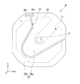
図1及び図2は、太陽電池モジュール10が適用された本実施形態の腕時計1000を示す図である。図1は平面図であり、図2は断面図である。
In this embodiment, a wristwatch is illustrated as a solar watch to which the
FIG.1 and FIG.2 is a figure which shows the
図1に示すように、本実施形態のソーラーウォッチとしての腕時計1000は、時計ケース1002と、時計ケース1002に連結された一対のバンド1003とを備えて構成されたものである。時計ケース1002は、ステンレス等の金属材又はプラスチック樹脂等の樹脂材で形成されたもので、その内部には、図2に示すように、ムーブメント(駆動部)1004と、時計用文字盤1005と、太陽電池モジュール10とが収容されている。
As shown in FIG. 1, a
時計ケース1002内の時計用文字盤1005側(時計表側,+Z側)には、樹脂製又は金属製の圧入リング(図示せず)を介して、ガラス製または樹脂製の透明カバー(図示せず)が圧入固定されている。また、時計ケース1002内のムーブメント1004側(時計裏側,−Z側)には、パッキン(図示せず)を介して裏蓋(図示せず)が螺合され、この裏蓋及び透明カバーによって時計ケース1002の内部の密封性が確保されている。
A transparent cover (not shown) made of glass or resin is provided on the
また、図1に示すように、時計ケース1002には、操作子としての竜頭1010と、2つの操作ボタン1011とが設けられている。竜頭1010は、多段階(本実施形態では2段階)で押し引き自在、かつ、回転自在に設けられたものである。
As shown in FIG. 1, the
図2に示すように、ムーブメント1004は、秒針1021と、分針1022と、時針1023と、電源装置1050とを備えている。秒針1021、分針1022及び時針1023は、同軸上に配列されている。すなわち、秒針1021、分針1022及び時針1023が設置されている各軸は、それぞれ同軸となるように設置されている。秒針1021、分針1022及び時針1023が設置される軸は、太陽電池モジュール10に形成された貫通孔41と、時計用文字盤1005に形成された貫通孔1005Aとを介して、時計用文字盤1005より上側(+Z側)に突出している。
電源装置1050は、ムーブメント1004に電力を供給する。電源装置1050は、太陽電池モジュール10によって充電される二次電池(図示せず)を含んでいる。
As shown in FIG. 2, the
The
時計用文字盤1005は、時刻を示す文字が表示された平板である。図1においては、12時、3時、6時、9時の時刻表示のみ示している。
時計用文字盤1005は、透光性を有している。時計用文字盤1005の光透過率は、例えば、20%である。
The
The
太陽電池モジュール10は、時計用文字盤1005と、ムーブメント1004との間に設けられている。
The
<太陽電池モジュール>
図3は太陽電池モジュール10の平面図であり、図4は太陽電池モジュール10の断面図である。
図3に示すように、本実施形態に係る太陽電池モジュール10は、太陽電池パネル20と、可撓性基板30とを備える。太陽電池パネル20は、太陽光を受けて発電する積層パネルである。本実施形態においては、太陽電池パネル20は、平面視(XY面視)で略正八角形状である。太陽電池パネル20の曲げ弾性は、可撓性基板30の曲げ弾性よりも大きい。なお、太陽電池パネル20の形状は、略正八角形に限定されるものではない。
<Solar cell module>
FIG. 3 is a plan view of the
As shown in FIG. 3, the
太陽電池パネル20には、線状の間隙からなる分割線部40と、時計の針を設置するための貫通孔41とが形成されている。太陽電池パネル20は、分割線部40によって、複数の個片に分割されている。分割線部40は、貫通孔41を通らないように形成されている。
The
本実施形態においては、太陽電池パネル20は、分割線部40により、第1個片(第1電池、太陽電池片)20aと、第2個片(第2電池、太陽電池片)20bとの2つの個片に分割されている。本実施形態において、第1個片20aは図3において平面視右側(+X方向)に配置されており、第2個片20bは平面視左側(−X方向)に配置されている。第1個片20aは、太陽電池パネル20の中心を含んでいる。貫通孔41は、太陽電池パネル20の中心に形成されている。したがって、貫通孔41は、第1個片20aに形成されている。
In the present embodiment, the
分割線部40の幅としては、例えば、0.1mm以上、0.3mm以下である。分割線部40の幅がこの値の範囲内であることにより、可撓性基板30の折れ曲がりをより抑制しやすい。なお、分割線部40の形状は図3の形態に限られない。すなわち、第1個片20a及び第2個片20bの形状は図3の形態に限られない。
The width of the
図4に示すように、太陽電池パネル20(第1個片20a及び第2個片20b)は、SUS基板(裏面側電極)21と、アルミニウム層(Al層)22と、酸化亜鉛層(ZnO層)23と、発電層24と、ITO膜層(透明導電膜層)25とが、この順で積層されて構成されている。太陽電池パネル20には、ITO膜層25側(+Z側)から光が入射する。なお、ITO膜層25(表面側電極)は、本実施形態においては、正極として機能する。
As shown in FIG. 4, the solar cell panel 20 (
一方、SUS基板21は、本実施形態においては、負極として機能する基板である。
アルミニウム層22は、酸化亜鉛層23側の表面に凹凸が形成され、ITO膜層25側(+Z側)から太陽電池パネル20に入射した太陽光のうち、発電層24を透過した光を散乱して反射する層である。
酸化亜鉛層23は、発電層24とアルミニウム層22との間で、光の屈折率を調整する層である。
On the other hand, the
The
The
発電層24は、例えば、本実施形態においては、3層構造(トリプルジャンクション構造)の多接合型の発電層である。発電層24は、酸化亜鉛層23側(−Z側)から順に、第1アモルファスシリコンゲルマニウム層(a−SiGe層)24aと、第2アモルファスシリコンゲルマニウム層24bと、アモルファスシリコン層(a−Si層)24cとを備える。
The
第1アモルファスシリコンゲルマニウム層24aと第2アモルファスシリコンゲルマニウム層24bとは、アモルファスシリコンにゲルマニウムがドープされることによって形成される。第1アモルファスシリコンゲルマニウム層24aと第2アモルファスシリコンゲルマニウム層24bとにドープされているゲルマニウムの量は、それぞれ異なっている。第1アモルファスシリコンゲルマニウム層24aと、第2アモルファスシリコンゲルマニウム層24bと、アモルファスシリコン層24cとは、それぞれ吸収波長域が異なるように設定されている。
本実施形態において、アルミニウム層22と、酸化亜鉛層23と、発電層24とを合わせて、太陽電池本体27と称する。
The first amorphous
In the present embodiment, the
ITO膜層25は、本実施形態においては、正極として機能する透明な導電膜層である。
In this embodiment, the
可撓性基板30は、第1個片20aと第2個片20bとを連結するようにして、太陽電池パネル20のSUS基板21に貼着されている。
図3に示すように、可撓性基板30は、平面視(XY面視)において、切欠き部31によって略正八角形の一部が欠けた形状である。
The
As shown in FIG. 3, the
切欠き部31は、平面視(XY面視)において、太陽電池パネル20の中心側の端部が円弧状となっている帯状の切欠きである。切欠き部31は、可撓性基板30の中心まで形成されている。可撓性基板30は、貫通孔41に可撓性基板30が重ならないように太陽電池パネル20に貼着されている。言い換えると、可撓性基板30は、切欠き部31内に貫通孔41が配置されるように太陽電池パネル20に貼着されている。
The
また、本実施形態においては図示していないが、太陽電池パネル20には日付窓用の貫通孔が形成されている場合がある。その場合には、可撓性基板30は、平面視(XY面視)において、日付窓用の貫通孔と重ならないようにして貼着される。また、可撓性基板30は、例えば、日付窓用の貫通孔が可撓性基板30の切欠き部31内に配置されるように貼着される。
Although not shown in the present embodiment, the
可撓性基板30の平面視(XY面視)における面積は、太陽電池パネル20の平面視(XY面視)における面積よりも小さい。また、可撓性基板30の曲げ弾性は、太陽電池パネル20の曲げ弾性よりも小さい。
The area of the
第1個片20a及び第2個片20bには、それぞれ平面視で略四角形の切欠26a,26bが形成されている。切欠26a,26bは、後述のように本実施形態の導通部材を取り付けるためのものである。第1個片20a及び第2個片20bは導通部材により直列接続されている。なお、図3においては、導通部材の図示を省略している。
The
<導通部材>
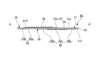
続いて、第1個片20a及び第2個片20bを直列接続する導通部材について説明する。図5は導通部材50の構成を示す図であり、図5(a)は導通部材50を裏面側から視た平面図であり、図5(b)は導通部材50を表面側から視た平面図であり、図5(c)は導通部材50を表面側から視た場合において、両面における導電層の配置関係を示した図である。図6は図5(c)のA−A’線矢視による導通部材50の断面構成を示す図である。なお、図5(c)では、図を見易くするため、導電層を覆う絶縁層の図示を省略している。
<Conductive member>
Next, a conductive member that connects the
図6に示すように、本実施形態の導通部材50は、フィルム基材(可撓性の基材)51と、フィルム基材51の裏面51b(一方の面)に配置された第1導電層52と、フィルム基材51の表面51a(他方の面)及び裏面51b(一方の面)の表裏両面に引き出された第2導電層53と、第1導電層52の一部を覆う絶縁層54と、第2導電層53の一部を覆う絶縁層55と、を備えている。第1導電層52及び第2導電層53は、例えば、銅箔等から構成される。
As shown in FIG. 6, the
図5(a)乃至(c)に示すように、フィルム基材51は、本体部56と、本体部56の両端に延出する第1延出部57及び第2延出部58と、を含む。第1延出部57及び第2延出部58の延出方向と交差する方向において、第1延出部57及び第2延出部58の幅よりも本体部56の幅のほうが大きい。第1延出部57は、第1個片20a及び第2個片20bを直列接続する際、第1個片20aに形成された切欠26aから引き出される。また、第2延出部58は、第1個片20a及び第2個片20bを直列接続する際、第2個片20bに形成された切欠26bから引き出される。
As shown in FIGS. 5A to 5C, the
図5(a)に示すように、第1導電層52は、裏面51b側において、本体部56から第1延出部57に至るように形成される。すなわち、本実施形態において、第1導電層52は、フィルム基材51の裏面51b側のみに形成される。第1導電層52は、一端側に設けられた第1接続部52aと、他端側に設けられた第2接続部52bと、これら第1接続部52a及び第2接続部52b間を接続する配線部52cと、を含む。第1接続部52aは、後述するように二次電池を含む電源装置1050(外部回路)の外部端子(入力端子)62に接続されるものである。第2接続部52bは、後述するように第1個片20aのITO膜層25と接続されるものである(図8参照)。絶縁層54は、第1接続部52aと第2接続部52bとの間の配線部52cの一部を覆うように、本体部56から第1延出部57に掛けて形成されている。なお、絶縁層54は、フィルム基材51の外縁に至るように形成されているが、これに限定されることはなく、配線部52cの一部を覆うように形成されていればよい。
As shown in FIG. 5A, the first
図5(b)に示すように、一方、第2導電層53は、表面51a側において本体部56から第2延出部58に至るように形成された配線部53aと、裏面51b側において第2延出部58に形成された第1接続部53b(図5(a)参照)と、配線部53aの本体部56側の端に形成された第2接続部53cとを含む。配線部53aの第2延出部58側の端には、スルーホール(貫通孔)51Hが形成されている。絶縁層55は、スルーホール51Hと第2接続部53cとの間の配線部53aの一部を覆うように、本体部56から第2延出部58に亘って形成されている。なお、絶縁層55は、フィルム基材51の外縁に至るように形成されているが、これに限定されることはなく、配線部53aの一部を覆うように形成されていればよい。
図5(c)に示すように、配線部53aと第1接続部53bとは、フィルム基材51に形成されたスルーホール(貫通孔)51Hを介して電気的に接続されている。すなわち、本実施形態において、第2導電層53は、フィルム基材51の表面51a及び裏面51bの両面に形成されている。これにより、第2導電層53は、フィルム基材51の表面51a側と裏面51b側とで電気的な導通を取ることを可能にしている。なお、配線部53aの第2接続部53cは、後述するように第1個片20aのSUS基板21(裏面側電極)に接続されるものである。第1接続部53bは、後述するように第2個片20bのITO膜層25(表面側電極)に接続されるものである(図8参照)。
On the other hand, as shown in FIG. 5B, the second
As shown in FIG. 5C, the
このような構成に基づいて、導通部材50は第1個片20a及び第2個片20bを直列接続可能となっている。図7は、太陽電池モジュール10における導通部材50の取り付け状態を示す図である。また、図8は図7のB−B’線矢視による断面図であり、導通部材50の太陽電池パネル20に対する接続構造の断面を示すものである。
Based on such a configuration, the
図7に示すように、導通部材50は、表面側(ITO膜層25が形成された面側)をそれぞれ上方に向けた状態の第1個片20a及び第2個片20b同士を導通(電気的に接続)する。導通部材50は、図8に示すように、導通(接続)時において、本体部56の表面51a側が太陽電池パネル20の裏面側に対向配置され、第1延出部57が切欠(第1の切欠)26aを介して太陽電池パネル20(第1個片20a)の表面側に引き出されると共に、第2延出部58が切欠(第2の切欠)26bを介して太陽電池パネル20(第2個片20b)の表面側に引き出される。
As shown in FIG. 7, the
本実施形態において、導通部材50は、フィルム基材51を主体に構成されるため、可撓性に優れている。そのため、導通部材50は、第1延出部57及び第2延出部58を上方に折り曲げることで切欠26a,26bを介して太陽電池パネル20の裏面側から表面側に容易に引き出すことができる。また、切欠26a,26bを介して太陽電池パネル20の表面に引き出された第1延出部57及び第2延出部58は、第1個片20a及び第2個片20bの上面(表面)に向けて容易に折り曲げられる。
In this embodiment, since the conducting
切欠26aを介して第1個片20aの上面に引き出された第1延出部57は、裏面51bに形成された第2接続部52b(第1導電層52)が第1個片20aのITO膜層25(正極)と電気的に接続される。本実施形態において、ITO膜層25及び第2接続部52bは導電性ペースト等の導通性材料60を介して電気的に接続される。
The first extending
また、第1導電層52は配線部52cを介して第2接続部52bと反対側に設けられた第1接続部52aが外部端子(電源装置1050の正極端子)62に電気的に接続される。外部端子62は、例えば、ばねピンから構成され、第1接続部52aに対して付勢力によって良好に接触した状態とされている。これにより、外部端子62及び第1接続部52aは、高い導通(接続)信頼性を備えている。
The first
すなわち、導通部材50は、第1導電層52により、第1個片20aのITO膜層25(正極)と、外部端子62(正極用入力端子)とを電気的に接続することができる。
That is, the
一方、切欠26bを介して第2個片20bの上面に引き出された第2延出部58は、裏面51bに形成された第2導電層53の第1接続部53bが第2個片20bのITO膜層25(正極)と電気的に接続される。本実施形態において、ITO膜層25及び第1接続部53bは導電性ペースト等の導通性材料60を介して接続されている。
On the other hand, the second extending
フィルム基材51は、本体部56の表面51aが第1個片20aの裏面に対向する。そのため、配線部53aの第2接続部53cが第1個片20aのSUS基板21(負極)と電気的に接続される。本実施形態において、第2接続部53c及びSUS基板21は導電性ペースト等の導通性材料60を介して電気的に接続される。
As for the
すなわち、導通部材50は、第2導電層53により、第1個片20aのSUS基板21(負極)と、第2個片20bのITO膜層25(正極)とを電気的に接続する。
That is, the
また、図8に示すように、第2個片20bのSUS基板21(負極)は、外部端子(電源装置1050の負極端子)61に電気的に接続される。外部端子61は、例えば、ばねピンから構成され、第2個片20bのSUS基板21に対して付勢力によって良好に接触した状態とされている。これにより、外部端子61及びSUS基板21は、高い導通(接続)信頼性を備えている。
As shown in FIG. 8, the SUS substrate 21 (negative electrode) of the
このように第1個片20aのSUS基板21と第2個片20bのITO膜層25とは、それぞれ二次電池を含む電源装置1050(外部回路)に電気的に接続される。すなわち、太陽電池モジュール10は、二次電池を含む電源装置1050に電気的に接続される。これにより、太陽電池モジュール10が発電した電力が電源装置1050の二次電池に蓄えられるようになっている。
Thus, the
ところで、本実施形態において、第1延出部57及び第2延出部58は、切欠26a,26bを介して太陽電池パネル20の表面側に引き出される際、切欠26a,26bの端部に接触する場合がある。ここで、第1個片20a及び第2個片20bは、側端面(切欠26a,26bの端部)にITO膜層25(正極)及びSUS基板21(負極)が露出した構造となっている。そのため、第1延出部57または第2延出部58の表面に形成された第1導電層52または第2導電層53が切欠26a,26bの端部に接触すると短絡が生じるおそれがある。
By the way, in this embodiment, when the
これに対し、本実施形態に係る導通部材50は、第1導電層52の一部を覆う絶縁層54と、第2導電層53の一部を覆う絶縁層55と、を備えている。すなわち、切欠26aを介して第1個片20aの表面側に引き出された第1延出部57は、配線部52cの一部が絶縁層54により覆われている。そのため、配線部52cと切欠26aの端面(第1個片20aの側端面)とが導通することによる短絡の発生が防止される。
In contrast, the
また、切欠26bを介して引き出された第2延出部58の表面51aに形成された第2導電層53の一部(配線部53aの一部)が絶縁層55により覆われている。そのため、配線部53aと切欠26bの端面(第2個片20bの側端面)とが導通することによる短絡の発生が防止される。さらに、絶縁層55は、配線部53aのうち、第2個片20bのSUS基板21に対向する部分を覆っている。そのため、配線部53a及びSUS基板21同士、すなわち第2個片20bの正極及び負極間が導通することによる短絡の発生が防止される。
In addition, a part of the second conductive layer 53 (a part of the
以上述べたように、本実施形態によれば、太陽電池モジュール10は、太陽電池パネル20の第1個片20aと第2個片20bとが導通部材50により直列接続している。すなわち、第1個片20aのITO膜層25(正極)と第2個片20bのSUS基板21(負極)との電気的な直列接続構造を1つの導通部材50によって実現している。よって、部品点数の削減、あるいは導通作業に伴う工数の削減を図ることができ、結果的にコスト低減を図ることができる。また、導通部材50は、フィルム基材51(可撓性の基材)を主体に構成されるため、第1導電層52及び第2導電層53の引き回しが簡便且つ確実に行われて、第1個片20a及び第2個片20b間における導通(接続)信頼性を向上させることができる。
As described above, according to the present embodiment, in the
腕時計1000に実装された太陽電池モジュール10は、時計用文字盤1005側(+Z側)から太陽光が照射されると、透光性を有する時計用文字盤1005を介して太陽光が照射される。これにより、太陽電池モジュール10が発電され、太陽電池モジュール10と電気的に接続された電源装置1050の二次電池が充電される。
また、本実施形態によれば、発電層24として、アモルファスシリコンゲルマニウムからなる層を含むトリプルジャンクション構造にしたことにより、太陽電池パネル20を2分割にして、直列接続した場合であっても、十分な電圧を得ることができる。
When the
Further, according to the present embodiment, the
したがって、本実施形態に係る腕時計1000によれば、上記太陽電池モジュール10を備えることで高い駆動電圧を得ることができる。よって、安定した電力により駆動可能な信頼性の高いソーラーウォッチとしての腕時計1000を低コストで提供することができる。
Therefore, according to the
さらに、図7に示すように、切欠26a,26bは、分割線部40を挟んで対向して配置され、導通部材50によって第1個片20aと第2個片20bとを直列接続したときに、導通部材50は第1個片20a及び第2個片20bの外縁からはみ出さない。言い換えれば、導通部材50が第1個片20a及び第2個片20bの外縁からはみ出さない位置において、第1延出部57を引き出す切欠26aが第1個片20aに形成され、第2延出部58を引き出す切欠26bが第2個片20bに形成されている。
これによれば、隣り合う第1個片20aと第2個片20bの隙間である分割線部40から導通部材50を引き出すことが困難であっても、それぞれの太陽電池片に設けられた切欠26a,26bから第1延出部57と第2延出部58とを引き出して、第1個片20a及び第2個片20bのそれぞれの表面側電極に接続させることができる。言い換えれば、第1個片20aと第2個片20bとを近づけて配置しても電気的に直列接続が可能な太陽電池モジュール10を提供することができる。
Further, as shown in FIG. 7, the
According to this, even if it is difficult to pull out the conducting
また、導通部材50による第1個片20aと第2個片20bとの接続距離を比較的に短くすることができる。つまり、導通部材50の配線抵抗による電力の損出を小さくすることが可能な太陽電池モジュール10を提供することができる。また、第1延出部57は平面視で略四角形の貫通孔である切欠26aから引き出され、同じく第2延出部58は平面視で略四角形の貫通孔である切欠26bから引き出されるので、第1延出部57及び第2延出部58の引き出し位置がずれ難く、外力によって接続信頼性が損なわれることを低減可能な太陽電池モジュール10を提供することができる。
Moreover, the connection distance of the
(第2実施形態)
<太陽電池モジュール>
続いて、第2実施形態に係る太陽電池モジュールについて説明する。本実施形態と第1実施形態との違いは、導通部材の構造であり、それ以外の構成は共通である。そのため、以下の説明では、第1実施形態と同一の部材及び共通の構成については同じ符号を付し、その詳細な説明については省略する。
(Second Embodiment)
<Solar cell module>
Then, the solar cell module which concerns on 2nd Embodiment is demonstrated. The difference between this embodiment and 1st Embodiment is the structure of a conduction | electrical_connection member, and a structure other than that is common. Therefore, in the following description, the same code | symbol is attached | subjected about the member same as 1st Embodiment, and a common structure, and it abbreviate | omits about the detailed description.
図9は第2実施形態に係る太陽電池モジュールの概略構成を示す図であり、図9(a)は導電部材が取り付けられた状態の太陽電池モジュールの要部拡大平面図であり、図9(b)は導電部材を取り外した状態の太陽電池モジュールの要部拡大平面図である。 FIG. 9 is a diagram showing a schematic configuration of the solar cell module according to the second embodiment, and FIG. 9A is an enlarged plan view of a main part of the solar cell module with the conductive member attached, and FIG. b) is an enlarged plan view of a main part of the solar cell module with the conductive member removed.
図9(a)に示すように、本実施形態に係る太陽電池モジュール110は、第1個片20a及び第2個片20bを有し、これら第1個片20a及び第2個片20bが導通部材150により直列接続されている。
As shown to Fig.9 (a), the
第1個片20a及び第2個片20bには、図9(b)に示すように、それぞれ切欠126a,126bが形成されている。切欠126a,126bは、図9(a)に示した導通部材150を取り付けるためのものである。
As shown in FIG. 9B, the
<導通部材>
図10は本実施形態に係る導通部材150の構成を示す図であり、図10(a)は導通部材150を裏面側から視た平面図であり、図10(b)は導通部材150を表面側から視た平面図であり、図10(c)は導通部材150を表面側から視た場合において、両面における導電層の配置関係を示した図である。図11は図10(c)のD−D’線矢視による導通部材150の断面構成を示す図である。図12は図9(a)のC−C’線矢視による断面図であり、導通部材150の太陽電池パネル20に対する接続構造の断面を示すものである。
<Conductive member>
10A and 10B are diagrams showing the configuration of the conducting
図10(a)乃至(c)及び図11に示すように、導通部材150は、可撓性の基材であるフィルム基材151と、フィルム基材151の表面151a(他方の面)及び裏面151b(一方の面)の表裏両面に引き出された第1導電層152及び第2導電層153とを備えている。第1導電層152及び第2導電層153は、例えば、銅箔等から構成される。
As shown in FIGS. 10A to 10C and FIG. 11, the
図10(a)乃至(c)に示すように、フィルム基材151は、本体部156と、本体部156の両端に延出する第1延出部157及び第2延出部158と、を含む。図10(b)に示すように、第1延出部157は、本体部156に対して右側に向かって延出するものであり、先端が二股状に分岐された分岐構造160を有している。分岐構造160は、第1分岐端部160aと第2分岐端部160bとを含む。第2延出部158は、本体部156に対して左斜め下方に向かって延出するものであり、先端が二股状に分岐された分岐構造161を有している。分岐構造161は、第1分岐端部161aと第2分岐端部161bとを含む。
As shown in FIGS. 10A to 10C, the
第1延出部157は、第1個片20a及び第2個片20bを直列接続する際、第1個片20aに形成された切欠126aを介して第1分岐端部160aのみが上面(表面)側に引き出される。一方、第2分岐端部160bは、第1個片20aの下面(裏面)側に配置される(図9(a)参照)。
When the
また、第2延出部158は、第1個片20a及び第2個片20bを直列接続する際、第2個片20bに形成された切欠126bを介して第1分岐端部161aのみが上面(表面)側に引き出される。一方、第2分岐端部161bは、第2個片20bの下面(裏面)側に配置される(図9(a)参照)。
In addition, when the
図10(a)乃至(c)及び図11に示すように、第1導電層152は、表面151a側において第1延出部157の第1分岐端部160aに形成された第1配線部152aと、裏面151b側において第1延出部157の第1分岐端部160aに形成される第1接続部152b、及び本体部156に形成される第2配線部152c及び第2接続部152dと、を有している。第1接続部152bは、第1個片20aのITO膜層25に接続されるものである。第2接続部152dは、後述のように二次電池を含む電源装置1050(外部回路)の外部端子(入力端子)62に接続されるものである(図12参照)。
As shown in FIGS. 10A to 10C and FIG. 11, the first
図10(c)に示すように、第1接続部152b及び第1配線部152aは、フィルム基材151に形成されたスルーホール151H1を介して電気的に接続されている。また、第1配線部152a及び第2配線部152cは、フィルム基材151に形成されたスルーホール151H2を介して電気的に接続されている。本実施形態において、第1導電層152は、フィルム基材151の表面151a及び裏面151bの両面に形成されている。これにより、第1導電層152は、フィルム基材151の表面151a側と裏面151b側とで電気的な導通を取ることを可能にしている。
As shown in FIG. 10C, the
図10(a)乃至(c)及び図11に示すように、第2導電層153は、裏面151b側において第2延出部158の第1分岐端部161aに形成された第1接続部153a及び第2配線部153cと、表面151a側において第2延出部158の第1分岐端部161aに形成された第1配線部153bと、表面151a側において本体部156に形成された第2接続部153dと、を有している。第1接続部153aは、第2個片20bのITO膜層25に接続されるものである。第2接続部153dは、第1個片20aのSUS基板21に接続されるものであり、表面151a側に形成された第1導電層152の第2接続部152dと平面視で重なっている。
As shown in FIGS. 10A to 10C and FIG. 11, the second
第1接続部153a及び第1配線部153bは、フィルム基材151に形成されたスルーホール151H3を介して電気的に接続されている。また、第1配線部153b及び第2配線部153cは、フィルム基材151に形成されたスルーホール151H4を介して電気的に接続されている。また、第2配線部153c及び第2接続部153dは、フィルム基材151に形成されたスルーホール151H5を介して電気的に接続されている。本実施形態において、第2導電層153は、フィルム基材151の表面151a及び裏面151bの両面に形成されている。これにより、第2導電層153は、フィルム基材151の表面151a側と裏面151b側とで電気的な導通を取ることが可能である。
The
この構成に基づき、第2導電層153は、第1個片20aのSUS基板21(負極)と第2個片20bのITO膜層25(正極)とを直列接続可能である。また、第1導電層152は、第1個片20aのITO膜層25と電源装置1050の外部端子(入力端子)62と接続可能である(図12参照)。
Based on this configuration, the second
図12に示すように、導通部材150は、導通(接続)時において、本体部156の表面151a側が太陽電池パネル20の裏面側に対向配置され、第1延出部157の一部が切欠126aを介して太陽電池パネル20(第1個片20a)の表面側に引き出されるとともに第2延出部158の一部が切欠126bを介して太陽電池パネル20(第2個片20b)の表面側に引き出される。
As shown in FIG. 12, when conducting (connecting) the conducting
具体的に、導通部材150は、図9(a)に示したように、第1延出部157のうち第1分岐端部160aのみが上面(表面)側に引き出されるとともに第2延出部158のうち第1分岐端部161aのみが切欠126bを介して太陽電池パネル20(第2個片20b)の上面(表面)側に引き出される。一方、第1延出部157の第2分岐端部160bは第1個片20aの下面(裏面)側に配置され、及び第2延出部158の第2分岐端部161bは第2個片20bの下面(裏面)側に配置される。フィルム基材151から構成された第1分岐端部160a及び第1分岐端部161aは可撓性に優れるため、容易に折り曲げ可能である。よって、第1分岐端部160a及び第1分岐端部161aは、それぞれ切欠126a,126bを介して太陽電池パネル20の裏面側から表面側に容易に引き出すことが可能である。また、切欠126a,126bを介して太陽電池パネル20の表面に引き出された第1分岐端部160a,161aは、第1個片20a及び第2個片20bの上面に向けて容易に折り曲げ可能である。
Specifically, as shown in FIG. 9A, the
切欠126aを介して第1個片20aの上面(表面)に引き出された第1分岐端部160aは、図9(a)及び図12に示すように、裏面151bに形成された第1接続部152b(第1導電層152)が第1個片20aのITO膜層25(正極)と電気的に接続される。本実施形態において、ITO膜層25及び第1接続部152bは導電性ペースト等の導通性材料60を介して電気的に接続される。第1接続部152bは、スルーホール151H1,151H2、及び第1配線部152aを経由して裏面151b側に形成された第2配線部152cに接続され、第2配線部152cに設けられた第2接続部152dを介して外部端子(電源装置1050の正極端子)62と電気的に接続される。
The
すなわち、導通部材150は、第1導電層152により、第1個片20aのITO膜層25(正極)と外部端子62とを電気的に接続する。
That is, the
一方、切欠126bを介して第2個片20bの上面に引き出された第1分岐端部161aは、図9(a)及び図12に示すように、裏面151bに形成された第2導電層153の第1接続部153aが第2個片20bのITO膜層25(正極)と電気的に接続される。本実施形態において、ITO膜層25及び第1接続部153aは導電性ペースト等の導通性材料60を介して接続されている。第1接続部153aは、スルーホール151H3,151H4,151H5、及び第1配線部153b並びに第2配線部153cを経由して表面151a側に形成された第2接続部153dに接続され、この第2接続部153dを介して第1個片20aのSUS基板21と電気的に接続される。
On the other hand, the
本実施形態において、第2接続部153dは、表面151a側に形成された第1導電層152の第2接続部152dと平面視で重なっている。第2接続部152dは、ばねピンから構成された外部端子62の付勢力(応力)により導通部材150を第1個片20aの裏面側に押し付けられている。これにより、第2接続部152dと平面視で重なる第2接続部153dは、外部端子62の付勢力によって第1個片20aのSUS基板21側に押し付けられる。よって、第2接続部153dは、導電性ペースト等の導通性材料60を用いなくても、第1個片20aのSUS基板21に対して高い導通(接続)信頼性を得ることができる。
In the present embodiment, the
すなわち、導通部材150は、第2導電層153により、第1個片20aのSUS基板21(負極)と第2個片20bのITO膜層25(正極)とを電気的に接続する。
That is, the
ところで、本実施形態において、第1延出部157及び第2延出部158は、切欠126a,126bを介して太陽電池パネル20の表面側に引き出される際、切欠126a,126bの端部に接触する場合がある。ここで、第1個片20a及び第2個片20bは、側端面(切欠126a,126bの端部)にITO膜層25(正極)及びSUS基板21(負極)が露出した構造となっている。そのため、第1延出部157または第2延出部158に形成された第1導電層152または第2導電層153が切欠126a,126bの端部に接触すると短絡が生じるおそれがある。
By the way, in this embodiment, when the
これに対し、本実施形態に係る導通部材150は、フィルム基材151にスルーホール151H1,151H2,151H3,151H4,151H5を形成することで、第1導電層152及び第2導電層153をフィルム基材151の両面に引き出した構成としている。
On the other hand, the
すなわち、切欠126aを介して引き出された第1延出部157は、第1導電層152のうち切欠126aの端面に対応する部分(端面に接触するおそれがある部分)がスルーホール151H1,151H2、及び第1配線部152aにより表面151a側に引き出されている。そのため、第1導電層152は、切欠126aの端面(第1個片20aの側端面)と接触することがなく、第1導電層152及び切欠126aが接触することによる短絡の発生が防止される。
That is, the first extending
また、切欠126b及び分割線部40の隙間を介して表面側に引き出された第2延出部158は、第1個片20a及び第2個片20bの側端面と接触するおそれがある。
第2延出部158は、第2導電層153のうち切欠126b(第2個片20b)の端面に対応する部分(端面に接触するおそれがある部分)がスルーホール151H3,151H4,及び第1配線部153bにより表面151a側に引き出されている。そのため、第2導電層153は、切欠126bの端面(第2個片20bの側端面)と接触することがなく、第2導電層153及び切欠126bが接触することによる短絡の発生が防止される。
また、第2延出部158は、第1個片20aの側端面に対応する部分(端面に接触するおそれがある部分)がスルーホール151H4,151H5,及び第2配線部153cにより裏面151b側に引き出されている。そのため、第2導電層153は、第1個片20aの側端面と接触することがなく、第2導電層153及び第1個片20aが接触することによる短絡の発生が防止される。
Moreover, the
In the second extending
The second extending
以上述べたように、本実施形態に係る導通部材150によれば、第1個片20aのITO膜層25(正極)と第2個片20bのSUS基板(負極)21との電気的な直列接続構造を1つの部材で実現することができる。よって、部品点数の削減、あるいは導通作業に伴う工数の削減を図ることができ、結果的にコスト低減を図ることができる。
As described above, according to the
また、本実施形態では、第2接続部153dと第2接続部152dとが平面視で重なる構造とすることで、外部端子62の付勢力(応力)を利用して第2接続部153dとSUS基板21とを導通させている。そのため、第2接続部153d及びSUS基板21間の導通性材料60を不要にしても良い。この場合、さらなるコスト低減を図ることができる。また、第2接続部153dと第2接続部152dとが平面視で重なる構造としたことで導通部材150のスペース効率が向上して小型化するため、コスト低減を図ることができる。
In the present embodiment, the second connecting
また、本実施形態では、第1個片20a及び第2個片20b(太陽電池パネル20)が導通部材150の分岐構造160,161によって良好に保持されるため、振動などの外力に対して優れた耐性を備えた信頼性の高い導通性を備えている。したがって、本実施形態に係る導通部材150を備えた腕時計によれば、低コストで安定した電力により駆動可能な信頼性の高いソーラーウォッチとなる。
Moreover, in this embodiment, since the
さらに図9(a)に示すように、切欠126a,126bは分割線部40を挟んで配置され、且つ切欠126bは、隣り合う第1個片20aと第2個片20bとの隙間である分割線部40の一部を成すように第2個片20bを切り欠いて形成されている。したがって、分割線部40の切欠126bが設けられた部分を利用して、第2延出部158側の第1分岐端部161aを引き出し、第1個片20aと第2個片20bとを導通部材150で直列接続できることから、第1個片20aと第2個片20bとの接続距離を、第1実施形態に比べてさらに短くすることができる。つまり、導通部材150の配線抵抗による電力の損出を抑えた太陽電池モジュール110を提供することができる。
また、導通部材150は、隣り合う第1個片20a及び第2個片20bの外縁に沿った辺部を有している。したがって、導通部材150により第1個片20aと第2個片20bとを接続したときに、導通部材150が第1個片20a及び第2個片20bの外縁から大きくはみ出すことがない。つまり、第1個片20aと第2個片20bとを導通部材150で接続したときに、導通部材150が第1個片20a及び第2個片20bの外縁からはみ出し難くなり、より小型な太陽電池モジュール110を提供できる。
Further, as shown in FIG. 9A, the
In addition, the
以上、本発明の一実施形態について説明したが、本発明の内容は上記実施形態に限定されることはなく、発明の主旨を逸脱しない範囲内において適宜変更可能である。
例えば、上記第1実施形態では、外部端子62と電気的に接続される第1導電層52の第1接続部52aと、第1個片20aのSUS基板21と電気的に接続される第2導電層53の第2接続部53cとが平面視で重ならない構成を例に挙げたが、第2実施形態と同様、第1接続部52aと第2接続部53cとが平面視で重なるように配置しても良い。これによれば、外部端子62の付勢力(応力)を利用して第2接続部53cを第1個片20aのSUS基板21(裏面側電極)に導通させることができるので、小型化及び低コスト化を実現することができる。
As mentioned above, although one Embodiment of this invention was described, the content of this invention is not limited to the said embodiment, In the range which does not deviate from the main point of invention, it can change suitably.
For example, in the first embodiment, the
また、上記第1実施形態では、第2導電層53がスルーホール51Hを介してフィルム基材51の表面51a側から裏面51b側に引き回される構成を例に挙げて説明したが、スルーホール51Hを形成しなくても良い。すなわち、切欠26bを介して表面51a側に引き出された第2延出部58の表面51a側を第2個片20bのITO膜層25に対向させるように折り曲げても良い。これによれば、スルーホール51Hにより第2導電層53を表裏両面側に引き出して形成する必要が無くなるので、導通部材50の低コスト化を図ることができる。
Moreover, in the said 1st Embodiment, although the 2nd
また、上記第2実施形態では、導通部材150にスルーホール151H1,151H2,151H3,151H4,151H5が5つ形成される場合を例に挙げたが、スルーホールの数はこれに限定されない。
In the second embodiment, the case where five through holes 151H1, 151H2, 151H3, 151H4, and 151H5 are formed in the
また、導通部材の第1延出部及び第2延出部を太陽電池パネル20の表面側に引き出す切欠の構成は、上記第1実施形態の構成と上記第2実施形態の構成とを組み合わせた構成としてもよい。例えば、太陽電池パネル20の第1個片20aに切欠としての貫通孔を形成し、第2個片20bに分割線部40の一部を成す切欠を形成してもよい。つまり、2つの切欠のうちの1つが貫通孔であってもよい。
Moreover, the structure of the notch which pulls out the 1st extension part and 2nd extension part of a conduction member to the surface side of the
また、上記実施形態の導通部材50(導通部材150)を備えた太陽電池モジュール10(太陽電池モジュール110)が適用される電子機器は、ソーラーウォッチとしての腕時計1000に限定されない。例えば、ウェアラブルな健康機器や医療機器などの情報端末に適用してもよい。
Moreover, the electronic device to which the solar cell module 10 (solar cell module 110) including the conductive member 50 (conductive member 150) of the above embodiment is applied is not limited to the
10,110…太陽電池モジュール、20a…第1個片(第1電池、太陽電池片)、20b…第2個片20b(第2電池、太陽電池片)、21…SUS基板(裏面側電極)、25…ITO膜層(表面側電極)、26a,126a…第1の切欠としての切欠、26b,126b…第2の切欠としての切欠、40…隙間としての分割線部、50,150…導通部材、51,151…フィルム基材(可撓性の基材)、51a,151a…表面(他方の面)、51b,151b…裏面(一方の面)、52,152…第1導電層、53,153…第2導電層、54,55…絶縁層、56,156…本体部、57,157…第1延出部、58,158…第2延出部、61,62…外部端子、51H,151H1,151H2,151H3,151H4,151H5…スルーホール、160a,161a…第1分岐端部、160b,161b…第2分岐端部、1000…腕時計(ソーラーウォッチ)、1004…駆動部としてのムーブメント、1050…電源装置。
DESCRIPTION OF SYMBOLS 10,110 ... Solar cell module, 20a ... 1st piece (1st battery, solar cell piece), 20b ...
Claims (16)
可撓性の基材と、
前記基材の一方の面に設けられた第1導電層と、
前記基材の他方の面に設けられ、前記基材を平面視した場合に前記第1導電層と重なる領域を有する第2導電層と、を備え、
前記基材を折り曲げて、前記第1導電層を前記第1電池の第1面側に設けられた第1電極に電気的に接続させ、前記第2導電層を前記第1電池の第2面側に設けられた第2電極と前記第2電池の第1面側に設けられた第3電極とに電気的に接続させることを特徴とする導通部材。 A conductive member that is arranged adjacent to each other and that electrically connects the first battery and the second battery, each having an electrode provided on the first surface side and the second surface side opposite to the first surface side. There,
A flexible substrate;
A first conductive layer provided on one surface of the substrate;
A second conductive layer provided on the other surface of the base material and having a region overlapping the first conductive layer when the base material is viewed in plan ,
The base material is bent to electrically connect the first conductive layer to a first electrode provided on the first surface side of the first battery, and the second conductive layer is connected to the second surface of the first battery. A conductive member characterized in that it is electrically connected to a second electrode provided on the side and a third electrode provided on the first surface side of the second battery.
前記基材は、本体部と、前記本体部から互いに異なる方向に延出した第1延出部及び第2延出部とを有し、
前記基材の前記第1延出部は、前記第1の切欠で折り曲げられて前記第1電池の第1面側に引き出され、前記第1導電層の前記第1延出部に設けられた部分が前記第1電池の第1電極に電気的に接続され、
前記基材の前記第2延出部は、前記第2の切欠で折り曲げられて前記第2電池の第1面側に引き出され、前記第2導電層の前記第2延出部に設けられた部分が前記第2電池の第3電極に電気的に接続され、
前記基材の前記本体部は、前記第1の切欠と前記第2の切欠との間で、前記第1電池及び前記第2電池の第2面側に位置し、前記第2導電層の前記本体部に設けられた部分が前記第1電池の第2電極に電気的に接続されることを特徴とする請求項1に記載の導通部材。 The first battery is provided with a first notch; the second battery is provided with a second notch;
The base material includes a main body part, and a first extension part and a second extension part that extend in different directions from the main body part,
The first extending portion of the base material is bent at the first notch and pulled out to the first surface side of the first battery, and is provided on the first extending portion of the first conductive layer. A portion is electrically connected to the first electrode of the first battery;
The second extending portion of the base material is bent at the second notch and pulled out to the first surface side of the second battery, and is provided on the second extending portion of the second conductive layer. A portion is electrically connected to the third electrode of the second battery;
The main body portion of the base material is located on a second surface side of the first battery and the second battery between the first notch and the second notch, and the second conductive layer The conductive member according to claim 1, wherein a portion provided in the main body is electrically connected to the second electrode of the first battery.
前記太陽電池モジュールからの電力により駆動する駆動部と、
を備えることを特徴とするソーラーウォッチ。 A solar cell module comprising a pair of solar cell pieces and the conducting member according to claim 5 for electrically connecting the pair of solar cell pieces in series;
A drive unit driven by electric power from the solar cell module;
Solar watch characterized by comprising.
前記一対の太陽電池片のうちの一方の太陽電池片の第1電極に電気的に接続された前記第1導電層と、前記一対の太陽電池片のうち他方の太陽電池片の第2面側に設けられた第4電極とが、前記電源装置に電気的に接続され、前記二次電池を充電可能となっていることを特徴とする請求項6または7に記載のソーラーウォッチ。 A power supply unit including a secondary battery,
The first conductive layer electrically connected to the first electrode of one solar cell piece of the pair of solar cell pieces, and the second surface side of the other solar cell piece of the pair of solar cell pieces. The solar watch according to claim 6 or 7, wherein a fourth electrode provided on the battery is electrically connected to the power supply device and can charge the secondary battery.
可撓性の基材と、前記基材の一方の面に設けられた第1導電層と、前記基材の他方の面に設けられ、前記基材を平面視した場合に前記第1導電層と重なる領域を有する第2導電層と、を含む導通部材と、を備え、
前記基材が折り曲げられて、前記第1導電層は前記第1太陽電池片の第1面側に設けられた第1電極に電気的に接続され、前記第2導電層は前記第1太陽電池片の第2面側に設けられた第2電極と前記第2太陽電池片の第1面側に設けられた第3電極とに電気的に接続されていることを特徴とする太陽電池モジュール。 A first solar cell piece and a second solar cell piece, which are arranged adjacent to each other and provided with electrodes on the first surface side and on the second surface side opposite to the first surface side,
A flexible base material, a first conductive layer provided on one surface of the base material, and a first conductive layer provided on the other surface of the base material when the base material is viewed in plan And a second conductive layer having a region overlapping with the conductive member.
The base material is bent, the first conductive layer is electrically connected to a first electrode provided on the first surface side of the first solar cell piece, and the second conductive layer is the first solar cell. A solar cell module, wherein the solar cell module is electrically connected to a second electrode provided on the second surface side of the piece and a third electrode provided on the first surface side of the second solar cell piece.
前記第2太陽電池片に設けられた第2の切欠と、を備え、
前記基材は、本体部と、前記本体部から互いに異なる方向に延出した第1延出部及び第2延出部とを有し、
前記基材の前記第1延出部は、前記第1の切欠で折り曲げられて前記第1電池の第1面側に引き出され、前記第1導電層の前記第1延出部に設けられた部分が前記第1電池の第1電極に電気的に接続され、
前記基材の前記第2延出部は、前記第2の切欠で折り曲げられて前記第2電池の第1面側に引き出され、前記第2導電層の前記第1延出部に設けられた部分が前記第2電池の第3電極に電気的に接続され、
前記基材の前記本体部は、前記第1の切欠と前記第2の切欠との間で、前記第1電池及び前記第2電池の第2面側に位置し、前記第2導電層の前記本体部に設けられた部分が前記第1電池の第2電極に電気的に接続されていることを特徴とする請求項9に記載の太陽電池モジュール。 A first notch provided in the first solar cell piece;
A second notch provided in the second solar cell piece,
The base material includes a main body part, and a first extension part and a second extension part that extend in different directions from the main body part,
The first extending portion of the base material is bent at the first notch and pulled out to the first surface side of the first battery, and is provided on the first extending portion of the first conductive layer. A portion is electrically connected to the first electrode of the first battery;
The second extending portion of the base material is bent at the second notch and pulled out to the first surface side of the second battery, and is provided on the first extending portion of the second conductive layer. A portion is electrically connected to the third electrode of the second battery;
The main body portion of the base material is located on a second surface side of the first battery and the second battery between the first notch and the second notch, and the second conductive layer The solar cell module according to claim 9, wherein a portion provided in the main body is electrically connected to the second electrode of the first battery.
前記第1延出部の前記第1分岐端部が前記第1の切欠から前記第1電池の第1面側に引き出され、前記第1導電層の前記第1分岐端部に設けられた部分が前記第1電池の第1電極に電気的に接続され、
前記第2延出部の前記第1分岐端部が前記第2の切欠から前記第2電池の第1面側に引き出され、前記第2導電層の前記第1分岐端部に設けられた部分が前記第2電池の第3電極に電気的に接続され、
前記第1延出部及び前記第2延出部の前記第2分岐端部は、隣り合う前記第1太陽電池片及び前記第2太陽電池片の第2面側に配置されていることを特徴とする請求項10乃至13のいずれか一項に記載の太陽電池モジュール。 Each of the first extension part and the second extension part has a first branch end part and a second branch end part,
The first branch end portion of the first extension portion is drawn from the first notch to the first surface side of the first battery, and is provided at the first branch end portion of the first conductive layer Is electrically connected to the first electrode of the first battery,
The first branch end portion of the second extension portion is drawn from the second notch to the first surface side of the second battery, and is provided at the first branch end portion of the second conductive layer Is electrically connected to the third electrode of the second battery,
The second branch end portions of the first extension portion and the second extension portion are disposed on the second surface side of the adjacent first solar cell piece and the second solar cell piece. The solar cell module according to any one of claims 10 to 13.
Priority Applications (3)
| Application Number | Priority Date | Filing Date | Title |
|---|---|---|---|
| JP2014171261A JP6488590B2 (en) | 2013-11-19 | 2014-08-26 | Conductive member, solar watch, solar cell module, electronic device |
| CN201410645841.8A CN104659135B (en) | 2013-11-19 | 2014-11-12 | Conductive member, solar watch, solar module, electronic equipment |
| US14/540,613 US9529331B2 (en) | 2013-11-19 | 2014-11-13 | Conductive member, solar watch, solar cell module, and electronic apparatus |
Applications Claiming Priority (3)
| Application Number | Priority Date | Filing Date | Title |
|---|---|---|---|
| JP2013238705 | 2013-11-19 | ||
| JP2013238705 | 2013-11-19 | ||
| JP2014171261A JP6488590B2 (en) | 2013-11-19 | 2014-08-26 | Conductive member, solar watch, solar cell module, electronic device |
Publications (3)
| Publication Number | Publication Date |
|---|---|
| JP2015121526A JP2015121526A (en) | 2015-07-02 |
| JP2015121526A5 JP2015121526A5 (en) | 2017-08-17 |
| JP6488590B2 true JP6488590B2 (en) | 2019-03-27 |
Family
ID=53173190
Family Applications (1)
| Application Number | Title | Priority Date | Filing Date |
|---|---|---|---|
| JP2014171261A Active JP6488590B2 (en) | 2013-11-19 | 2014-08-26 | Conductive member, solar watch, solar cell module, electronic device |
Country Status (3)
| Country | Link |
|---|---|
| US (1) | US9529331B2 (en) |
| JP (1) | JP6488590B2 (en) |
| CN (1) | CN104659135B (en) |
Families Citing this family (1)
| Publication number | Priority date | Publication date | Assignee | Title |
|---|---|---|---|---|
| CN112510106B (en) * | 2020-12-18 | 2021-08-03 | 中山德华芯片技术有限公司 | Manufacturing method of flexible solar cell module |
Family Cites Families (26)
| Publication number | Priority date | Publication date | Assignee | Title |
|---|---|---|---|---|
| US3427797A (en) * | 1966-12-12 | 1969-02-18 | Kenjiro Kimura | Timepiece using a solar battery as the power source |
| JPS5029954Y1 (en) * | 1970-12-29 | 1975-09-03 | ||
| JPS5353491Y2 (en) * | 1973-03-27 | 1978-12-21 | ||
| JPS5930466Y2 (en) * | 1977-08-10 | 1984-08-30 | シチズン時計株式会社 | Electrical connection structure of solar cells |
| JPS5678180A (en) * | 1979-11-30 | 1981-06-26 | Hitachi Ltd | Light receiving device |
| US4483910A (en) * | 1983-04-08 | 1984-11-20 | Julian Victor J | Sealed battery cable termination |
| TW387152B (en) * | 1996-07-24 | 2000-04-11 | Tdk Corp | Solar battery and manufacturing method thereof |
| JPH11186577A (en) | 1997-12-19 | 1999-07-09 | Dainippon Printing Co Ltd | Thin-film solar cell and manufacture thereof |
| JPH11186572A (en) * | 1997-12-22 | 1999-07-09 | Canon Inc | Photoelectromotive force element module |
| JP2001015781A (en) * | 1999-06-29 | 2001-01-19 | Sanyo Electric Co Ltd | Solar battery for clock |
| JP2002034125A (en) * | 2000-07-19 | 2002-01-31 | Yazaki Corp | Wiring unit |
| JP4021218B2 (en) * | 2001-04-24 | 2007-12-12 | セイコーエプソン株式会社 | Electronic clock |
| JP3729122B2 (en) * | 2001-11-09 | 2005-12-21 | 日産自動車株式会社 | Power wiring structure |
| JP2005324517A (en) * | 2004-05-17 | 2005-11-24 | Casio Comput Co Ltd | Decorative device and electronic equipment |
| JP2006084317A (en) | 2004-09-16 | 2006-03-30 | Citizen Watch Co Ltd | Solar cell and electronic timepiece with solar cell |
| DE602005017620D1 (en) * | 2005-09-06 | 2009-12-24 | Eta Sa Mft Horlogere Suisse | Watch with a semiconductive dial |
| DE102007011403A1 (en) * | 2007-03-08 | 2008-09-11 | Fraunhofer-Gesellschaft zur Förderung der angewandten Forschung e.V. | Front side series connected solar module |
| JP2008224482A (en) | 2007-03-14 | 2008-09-25 | Citizen Holdings Co Ltd | Electronic watch with solar cell |
| JP2012074676A (en) * | 2010-09-02 | 2012-04-12 | Seiko Instruments Inc | Solar panel, wristwatch, and method for manufacturing solar panel |
| US9147788B2 (en) * | 2010-09-07 | 2015-09-29 | Dow Global Technologies Llc | Photovoltaic cell assembly |
| JP5741948B2 (en) * | 2011-11-11 | 2015-07-01 | 株式会社オートネットワーク技術研究所 | Battery wiring module |
| JP2013122423A (en) | 2011-12-12 | 2013-06-20 | Seiko Epson Corp | Movement and electronic watch |
| JP2013195269A (en) | 2012-03-21 | 2013-09-30 | Casio Comput Co Ltd | Solar power generator and electronic watch |
| JP5888071B2 (en) * | 2012-04-02 | 2016-03-16 | カシオ計算機株式会社 | Solar power generator and electronic watch |
| JP6008181B2 (en) * | 2012-09-04 | 2016-10-19 | カシオ計算機株式会社 | Solar panels and watches |
| JP6048222B2 (en) * | 2013-03-04 | 2016-12-21 | カシオ計算機株式会社 | Solar panels and watches |
-
2014
- 2014-08-26 JP JP2014171261A patent/JP6488590B2/en active Active
- 2014-11-12 CN CN201410645841.8A patent/CN104659135B/en active Active
- 2014-11-13 US US14/540,613 patent/US9529331B2/en active Active
Also Published As
| Publication number | Publication date |
|---|---|
| JP2015121526A (en) | 2015-07-02 |
| US9529331B2 (en) | 2016-12-27 |
| US20150138935A1 (en) | 2015-05-21 |
| CN104659135A (en) | 2015-05-27 |
| CN104659135B (en) | 2017-07-07 |
Similar Documents
| Publication | Publication Date | Title |
|---|---|---|
| CN102422338B (en) | Display device | |
| US10056516B2 (en) | Solar panel | |
| US8873345B2 (en) | Solar power generating device and electronic timepiece | |
| JP2009129225A (en) | Touch panel | |
| CN104716212A (en) | Solar clock | |
| JP6488590B2 (en) | Conductive member, solar watch, solar cell module, electronic device | |
| JP2020013844A (en) | Photoelectric conversion element, photoelectric conversion module, and electronic device | |
| JP2016118404A (en) | Watch with solar cell | |
| JP2015060907A (en) | Solar cell module, clock and electronic apparatus | |
| JP7176265B2 (en) | Back electrode type photoelectric conversion element, photoelectric conversion module and electronic device | |
| JP2016092255A (en) | Solar cell module and electronic watch | |
| CN109889156B (en) | Solar panel | |
| JP5962252B2 (en) | Electronic clock with solar battery | |
| JP2015122475A (en) | Method for manufacturing solar cell module, and solar cell module | |
| JP5858676B2 (en) | Parts fixing structure | |
| JP4814007B2 (en) | clock | |
| JP4397092B2 (en) | Electronic device and solar cell module | |
| JP2019160822A (en) | Photoelectric conversion element, photoelectric conversion module and electronic equipment | |
| JP2013029468A5 (en) | ||
| JP6291909B2 (en) | Solar cell module and electronic watch | |
| JP2008224482A (en) | Electronic watch with solar cell | |
| JP4551531B2 (en) | Electronic clock with solar battery | |
| JP5208017B2 (en) | Electronic watch with solar cell | |
| JP2023092703A (en) | Electronic device | |
| JP6265232B2 (en) | Electronic clock with solar battery |
Legal Events
| Date | Code | Title | Description |
|---|---|---|---|
| RD03 | Notification of appointment of power of attorney |
Free format text: JAPANESE INTERMEDIATE CODE: A7423 Effective date: 20160622 |
|
| A521 | Written amendment |
Free format text: JAPANESE INTERMEDIATE CODE: A523 Effective date: 20170630 |
|
| A621 | Written request for application examination |
Free format text: JAPANESE INTERMEDIATE CODE: A621 Effective date: 20170630 |
|
| A977 | Report on retrieval |
Free format text: JAPANESE INTERMEDIATE CODE: A971007 Effective date: 20180525 |
|
| A131 | Notification of reasons for refusal |
Free format text: JAPANESE INTERMEDIATE CODE: A131 Effective date: 20180605 |
|
| A521 | Written amendment |
Free format text: JAPANESE INTERMEDIATE CODE: A523 Effective date: 20180803 |
|
| RD05 | Notification of revocation of power of attorney |
Free format text: JAPANESE INTERMEDIATE CODE: A7425 Effective date: 20180904 |
|
| RD03 | Notification of appointment of power of attorney |
Free format text: JAPANESE INTERMEDIATE CODE: A7423 Effective date: 20181107 |
|
| TRDD | Decision of grant or rejection written | ||
| A01 | Written decision to grant a patent or to grant a registration (utility model) |
Free format text: JAPANESE INTERMEDIATE CODE: A01 Effective date: 20190129 |
|
| A61 | First payment of annual fees (during grant procedure) |
Free format text: JAPANESE INTERMEDIATE CODE: A61 Effective date: 20190211 |
|
| R150 | Certificate of patent or registration of utility model |
Ref document number: 6488590 Country of ref document: JP Free format text: JAPANESE INTERMEDIATE CODE: R150 |