JP6436233B2 - Power receiver and power transmission system - Google Patents

Power receiver and power transmission system Download PDF

Info

Publication number
JP6436233B2
JP6436233B2 JP2017521453A JP2017521453A JP6436233B2 JP 6436233 B2 JP6436233 B2 JP 6436233B2 JP 2017521453 A JP2017521453 A JP 2017521453A JP 2017521453 A JP2017521453 A JP 2017521453A JP 6436233 B2 JP6436233 B2 JP 6436233B2
Authority
JP
Japan
Prior art keywords
power
phase
resonance coil
capacitor
switch
Prior art date
Legal status (The legal status is an assumption and is not a legal conclusion. Google has not performed a legal analysis and makes no representation as to the accuracy of the status listed.)
Active
Application number
JP2017521453A
Other languages
Japanese (ja)
Other versions
JPWO2016194202A1 (en
Inventor
弘敬 大島
弘敬 大島
聡 下川
聡 下川
昭嘉 内田
昭嘉 内田
Current Assignee (The listed assignees may be inaccurate. Google has not performed a legal analysis and makes no representation or warranty as to the accuracy of the list.)
Fujitsu Ltd
Original Assignee
Fujitsu Ltd
Priority date (The priority date is an assumption and is not a legal conclusion. Google has not performed a legal analysis and makes no representation as to the accuracy of the date listed.)
Filing date
Publication date
Application filed by Fujitsu Ltd filed Critical Fujitsu Ltd
Publication of JPWO2016194202A1 publication Critical patent/JPWO2016194202A1/en
Application granted granted Critical
Publication of JP6436233B2 publication Critical patent/JP6436233B2/en
Active legal-status Critical Current
Anticipated expiration legal-status Critical

Links

Images

Classifications

    • HELECTRICITY
    • H02GENERATION; CONVERSION OR DISTRIBUTION OF ELECTRIC POWER
    • H02JCIRCUIT ARRANGEMENTS OR SYSTEMS FOR SUPPLYING OR DISTRIBUTING ELECTRIC POWER; SYSTEMS FOR STORING ELECTRIC ENERGY
    • H02J50/00Circuit arrangements or systems for wireless supply or distribution of electric power
    • H02J50/10Circuit arrangements or systems for wireless supply or distribution of electric power using inductive coupling
    • H02J50/12Circuit arrangements or systems for wireless supply or distribution of electric power using inductive coupling of the resonant type
    • HELECTRICITY
    • H02GENERATION; CONVERSION OR DISTRIBUTION OF ELECTRIC POWER
    • H02JCIRCUIT ARRANGEMENTS OR SYSTEMS FOR SUPPLYING OR DISTRIBUTING ELECTRIC POWER; SYSTEMS FOR STORING ELECTRIC ENERGY
    • H02J50/00Circuit arrangements or systems for wireless supply or distribution of electric power
    • H02J50/40Circuit arrangements or systems for wireless supply or distribution of electric power using two or more transmitting or receiving devices
    • HELECTRICITY
    • H02GENERATION; CONVERSION OR DISTRIBUTION OF ELECTRIC POWER
    • H02MAPPARATUS FOR CONVERSION BETWEEN AC AND AC, BETWEEN AC AND DC, OR BETWEEN DC AND DC, AND FOR USE WITH MAINS OR SIMILAR POWER SUPPLY SYSTEMS; CONVERSION OF DC OR AC INPUT POWER INTO SURGE OUTPUT POWER; CONTROL OR REGULATION THEREOF
    • H02M7/00Conversion of ac power input into dc power output; Conversion of dc power input into ac power output
    • H02M7/02Conversion of ac power input into dc power output without possibility of reversal
    • H02M7/04Conversion of ac power input into dc power output without possibility of reversal by static converters
    • H02M7/06Conversion of ac power input into dc power output without possibility of reversal by static converters using discharge tubes without control electrode or semiconductor devices without control electrode
    • HELECTRICITY
    • H02GENERATION; CONVERSION OR DISTRIBUTION OF ELECTRIC POWER
    • H02MAPPARATUS FOR CONVERSION BETWEEN AC AND AC, BETWEEN AC AND DC, OR BETWEEN DC AND DC, AND FOR USE WITH MAINS OR SIMILAR POWER SUPPLY SYSTEMS; CONVERSION OF DC OR AC INPUT POWER INTO SURGE OUTPUT POWER; CONTROL OR REGULATION THEREOF
    • H02M3/00Conversion of dc power input into dc power output
    • H02M3/01Resonant DC/DC converters
    • H02M3/015Resonant DC/DC converters with means for adaptation of resonance frequency, e.g. by modification of capacitance or inductance of resonance circuit
    • HELECTRICITY
    • H02GENERATION; CONVERSION OR DISTRIBUTION OF ELECTRIC POWER
    • H02MAPPARATUS FOR CONVERSION BETWEEN AC AND AC, BETWEEN AC AND DC, OR BETWEEN DC AND DC, AND FOR USE WITH MAINS OR SIMILAR POWER SUPPLY SYSTEMS; CONVERSION OF DC OR AC INPUT POWER INTO SURGE OUTPUT POWER; CONTROL OR REGULATION THEREOF
    • H02M7/00Conversion of ac power input into dc power output; Conversion of dc power input into ac power output
    • H02M7/42Conversion of dc power input into ac power output without possibility of reversal
    • H02M7/44Conversion of dc power input into ac power output without possibility of reversal by static converters
    • H02M7/48Conversion of dc power input into ac power output without possibility of reversal by static converters using discharge tubes with control electrode or semiconductor devices with control electrode
    • H02M7/4815Resonant converters
    • H02M7/4818Resonant converters with means for adaptation of resonance frequency, e.g. by modification of capacitance or inductance of resonance circuits
    • YGENERAL TAGGING OF NEW TECHNOLOGICAL DEVELOPMENTS; GENERAL TAGGING OF CROSS-SECTIONAL TECHNOLOGIES SPANNING OVER SEVERAL SECTIONS OF THE IPC; TECHNICAL SUBJECTS COVERED BY FORMER USPC CROSS-REFERENCE ART COLLECTIONS [XRACs] AND DIGESTS
    • Y02TECHNOLOGIES OR APPLICATIONS FOR MITIGATION OR ADAPTATION AGAINST CLIMATE CHANGE
    • Y02BCLIMATE CHANGE MITIGATION TECHNOLOGIES RELATED TO BUILDINGS, e.g. HOUSING, HOUSE APPLIANCES OR RELATED END-USER APPLICATIONS
    • Y02B70/00Technologies for an efficient end-user side electric power management and consumption
    • Y02B70/10Technologies improving the efficiency by using switched-mode power supplies [SMPS], i.e. efficient power electronics conversion e.g. power factor correction or reduction of losses in power supplies or efficient standby modes

Description

本発明は、受電器、及び、電力伝送システムに関する。   The present invention relates to a power receiver and a power transmission system.

従来より、給電元の共鳴素子から共鳴により非接触で交流電力の供給を受ける共鳴素子と、前記共鳴素子から電磁誘導により交流電力の供給を受ける励振素子と、前記励振素子からの交流電力から直流電力を生成して出力する整流回路と、前記整流回路への交流電力の供給/非供給を切り替える切替回路とを備える非接触受電装置がある(例えば、特許文献1参照)。   Conventionally, a resonant element that is contactlessly supplied with alternating-current power by resonance from a resonance element that is a power supply source, an excitation element that is supplied with alternating-current power by electromagnetic induction from the resonant element, and a direct current from the alternating-current power from the excitation element There is a non-contact power receiving apparatus including a rectifier circuit that generates and outputs electric power and a switching circuit that switches supply / non-supply of AC power to the rectifier circuit (see, for example, Patent Document 1).

特開2011−019291号公報JP 2011-019291 A

ところで、従来の非接触受電装置(受電器)は、共鳴素子が受電する受電電力の調整を考慮していない。受電電力を調整できれば、送電器と受電器との間で効率的に電力を伝送できる。   By the way, the conventional non-contact power receiving device (power receiver) does not consider the adjustment of the received power received by the resonant element. If the received power can be adjusted, the power can be efficiently transmitted between the power transmitter and the power receiver.

そこで、受電電力を調整できる受電器、及び、電力伝送システムを提供することを目的とする。   Then, it aims at providing the power receiver which can adjust received power, and a power transmission system.

本発明の実施の形態の受電器は、共振コイル部を有し、一次側共振コイルとの間で生じる磁界共鳴又は電界共鳴によって前記一次側共振コイルから電力を受電する二次側共振コイルと、前記二次側共振コイルの前記共振コイル部に直列に挿入されるキャパシタと、前記キャパシタに並列に接続される、第1スイッチ及び第2スイッチの直列回路と、前記第1スイッチに並列に接続され、第1整流方向を有する第1整流素子と、前記第2スイッチに並列に接続され、前記第1整流方向とは反対の第2整流方向を有する第2整流素子と、前記二次側共振コイルが受電する電力を検出する検出部と、前記第1スイッチのオン/オフを切り替える第1信号及び前記第2スイッチのオン/オフを切り替える第2信号の前記二次側共振コイルが受電する電力の位相に対する位相を調整することにより、前記二次側共振コイルが受電する電力量を調整する、制御部とを含前記制御部は、前記検出部によって検出される電力に基づき、前記電力のうなりの周波数が低下するように、前記第1信号及び前記第2信号のスイッチング周波数を調整する
A power receiver according to an embodiment of the present invention has a resonance coil unit, and receives a power from the primary resonance coil by magnetic field resonance or electric field resonance generated between the primary resonance coil, and a secondary resonance coil, A capacitor inserted in series in the resonance coil section of the secondary resonance coil, a series circuit of a first switch and a second switch connected in parallel to the capacitor, and connected in parallel to the first switch A first rectifying element having a first rectifying direction, a second rectifying element connected in parallel to the second switch and having a second rectifying direction opposite to the first rectifying direction, and the secondary resonance coil conductive but that a detector for detecting the power to the power receiving, the first first signal and the secondary side resonance coil of the second signal for switching on / off the second switch for switching the on / off switch is powered By adjusting the phase of the relative phase, adjusts the amount of power the secondary side resonance coil receives power, seen including a control unit, based on the power detected by the detecting unit, the power The switching frequency of the first signal and the second signal is adjusted so that the beat frequency decreases .

受電電力を調整できる受電器、及び、電力伝送システムを提供することができる。   A power receiver capable of adjusting received power and a power transmission system can be provided.

電力伝送システムを示す図である。It is a figure which shows an electric power transmission system. 送電器から電子機器に磁界共鳴によって電力を伝送する状態を示す図である。It is a figure which shows the state which transmits electric power from a power transmission device to an electronic device by magnetic field resonance. 送電器から電子機器に磁界共鳴によって電力を伝送する状態を示す図である。It is a figure which shows the state which transmits electric power from a power transmission device to an electronic device by magnetic field resonance. 実施の形態1の受電器と送電装置を示す図である。3 is a diagram illustrating a power receiver and a power transmission device according to Embodiment 1. FIG. 制御部の内部構成を示す図である。It is a figure which shows the internal structure of a control part. キャパシタ及び調整部における電流経路を示す図である。It is a figure which shows the electric current path in a capacitor and an adjustment part. 二次側共振コイルに生じる交流電圧と、駆動信号に含まれる2つのクロックを示す図である。It is a figure which shows the alternating voltage which arises in a secondary side resonance coil, and two clocks contained in a drive signal. 駆動信号の位相に対する受電効率の特性を示すシミュレーション結果を示す図である。It is a figure which shows the simulation result which shows the characteristic of the power receiving efficiency with respect to the phase of a drive signal. 実施の形態1の電力伝送システムを用いた送電装置と電子機器を示す図である。2 is a diagram illustrating a power transmission device and an electronic device using the power transmission system according to Embodiment 1. FIG. 駆動信号の位相と、受電器の受電電力量との関係を示す図である。It is a figure which shows the relationship between the phase of a drive signal, and the received electric energy of a receiving device. 受電器が受電する電力(受電電力)のうなりを示す図である。It is a figure which shows the beat of the electric power (received electric power) which a receiving device receives. 受電器が受電する電力(受電電力)のうなりを示す図である。It is a figure which shows the beat of the electric power (received electric power) which a receiving device receives. 実施の形態1の受電器でうなりの影響を緩和する手法を示す図である。3 is a diagram illustrating a technique for reducing the influence of beat by the power receiver according to Embodiment 1. FIG. 実施の形態1の受電器でうなりの影響を緩和する手法を示す図である。3 is a diagram illustrating a technique for reducing the influence of beat by the power receiver according to Embodiment 1. FIG. 位相の原点を見つける手法を示す図である。It is a figure which shows the method of finding the origin of a phase. 送電器と受電器とが位相を設定するために実行する処理を示すタスク図である。It is a task figure showing processing which a power transmitter and a power receiver perform in order to set up a phase. 送電装置と電子機器の等価回路を示す図である。It is a figure which shows the equivalent circuit of a power transmission apparatus and an electronic device. 相互インダクタンスMTAと相互インダクタンスMTBとの関係に対して、位相を関連付けたテーブルデータを示す図である。It is a figure which shows the table data which linked | related the phase with respect to the relationship between the mutual inductance MTA and the mutual inductance MTB . 相互インダクタンスMTA、MTBと、受電効率とを関連付けたテーブルデータである。This is table data in which mutual inductances M TA and M TB are associated with power reception efficiency. 実施の形態1の送電器が受電器の位相を設定する方法を示すフローチャートである。4 is a flowchart illustrating a method for setting the phase of the power receiver by the power transmitter according to the first embodiment. 受電器が実行する処理を示すフローチャートである。It is a flowchart which shows the process which a power receiving device performs. 受電器が実行する処理を示すフローチャートである。It is a flowchart which shows the process which a power receiving device performs. 受電器が実行する処理を示すフローチャートである。It is a flowchart which shows the process which a power receiving device performs. 受電器が実行する処理を示すフローチャートである。It is a flowchart which shows the process which a power receiving device performs. 実施の形態1の変形例の調整部を示す図である。FIG. 10 is a diagram showing an adjustment unit of a modification of the first embodiment. キャパシタ及び調整部における電流経路を示す図である。It is a figure which shows the electric current path in a capacitor and an adjustment part. 実施の形態2の受電器と送電装置を示す図である。FIG. 6 illustrates a power receiver and a power transmission device according to a second embodiment. キャパシタ及び調整部における電流経路を示す図である。It is a figure which shows the electric current path in a capacitor and an adjustment part. 実施の形態2の変形例の調整部を示す図である。FIG. 10 is a diagram illustrating an adjustment unit according to a modification of the second embodiment. 実施の形態2の変形例の調整部を示す図である。FIG. 10 is a diagram illustrating an adjustment unit according to a modification of the second embodiment. キャパシタ及び調整部における電流経路を示す図である。It is a figure which shows the electric current path in a capacitor and an adjustment part.

以下、本発明の受電器、及び、電力伝送システムを適用した実施の形態について説明する。   Embodiments to which the power receiver and the power transmission system of the present invention are applied will be described below.

<実施の形態1>
本発明の受電器、及び、電力伝送システムを適用した実施の形態1について説明する前に、図1乃至図3を用いて、実施の形態1の受電器、及び、電力伝送システムの前提技術について説明する。
<Embodiment 1>
Before describing the first embodiment to which the power receiver and the power transmission system of the present invention are applied, the prerequisite technology of the power receiver and the power transmission system according to the first embodiment will be described with reference to FIGS. 1 to 3. explain.

図1は、電力伝送システム50を示す図である。   FIG. 1 is a diagram illustrating a power transmission system 50.

図1に示すように、電力伝送システム50は、交流電源1、一次側(送電側)の送電器10、及び二次側(受電側)の受電器20を含む。電力伝送システム50は、送電器10及び受電器20を複数含んでもよい。   As shown in FIG. 1, the power transmission system 50 includes an AC power source 1, a primary side (power transmission side) power transmitter 10, and a secondary side (power reception side) power receiver 20. The power transmission system 50 may include a plurality of power transmitters 10 and power receivers 20.

送電器10は、一次側コイル11と一次側共振コイル12を有する。受電器20は、二次側共振コイル21と二次側コイル22を有する。二次側コイル22には負荷装置30が接続される。   The power transmitter 10 includes a primary side coil 11 and a primary side resonance coil 12. The power receiver 20 includes a secondary side resonance coil 21 and a secondary side coil 22. A load device 30 is connected to the secondary coil 22.

図1に示すように、送電器10及び受電器20は、一次側共振コイル(LC共振器)12と二次側共振コイル(LC共振器)21の間の磁界共鳴(磁界共振)により、送電器10から受電器20へエネルギー(電力)の伝送を行う。ここで、一次側共振コイル12から二次側共振コイル21への電力伝送は、磁界共鳴だけでなく電界共鳴(電界共振)等も可能であるが、以下の説明では、主として磁界共鳴を例として説明する。   As shown in FIG. 1, the power transmitter 10 and the power receiver 20 transmit power by magnetic field resonance (magnetic field resonance) between a primary side resonance coil (LC resonator) 12 and a secondary side resonance coil (LC resonator) 21. Energy (electric power) is transmitted from the electric device 10 to the electric power receiver 20. Here, the power transmission from the primary side resonance coil 12 to the secondary side resonance coil 21 can be performed not only by magnetic field resonance but also by electric field resonance (electric field resonance). However, in the following description, magnetic field resonance is mainly used as an example. explain.

また、実施の形態1では、一例として、交流電源1が出力する交流電圧の周波数が6.78MHzであり、一次側共振コイル12と二次側共振コイル21の共振周波数が6.78MHzである場合について説明する。   In the first embodiment, as an example, the frequency of the AC voltage output from the AC power supply 1 is 6.78 MHz, and the resonance frequency of the primary side resonance coil 12 and the secondary side resonance coil 21 is 6.78 MHz. Will be described.

なお、一次側コイル11から一次側共振コイル12への電力伝送は電磁誘導を利用して行われ、また、二次側共振コイル21から二次側コイル22への電力伝送も電磁誘導を利用して行われる。   Note that power transmission from the primary side coil 11 to the primary side resonance coil 12 is performed using electromagnetic induction, and power transmission from the secondary side resonance coil 21 to the secondary side coil 22 also uses electromagnetic induction. Done.

また、図1には、電力伝送システム50が二次側コイル22を含む形態を示すが、電力伝送システム50は二次側コイル22を含まなくてもよく、この場合には、二次側共振コイル21に負荷装置30を直接的に接続すればよい。   1 shows a form in which the power transmission system 50 includes the secondary side coil 22, the power transmission system 50 may not include the secondary side coil 22. In this case, the secondary side resonance What is necessary is just to connect the load apparatus 30 to the coil 21 directly.

図2は、送電器10から電子機器40A、40Bに磁界共鳴によって電力を伝送する状態を示す図である。   FIG. 2 is a diagram illustrating a state in which power is transmitted from the power transmitter 10 to the electronic devices 40A and 40B by magnetic field resonance.

電子機器40A及び40Bは、それぞれ、タブレットコンピュータ及びスマートフォンであり、それぞれ、受電器20A、20Bを内蔵している。受電器20A及び20Bは、図1に示す受電器20(図1参照)から二次側コイル22を取り除いた構成を有する。すなわち、受電器20A及び20Bは、二次側共振コイル21を有する。なお、図2では送電器10を簡略化して示すが、送電器10は交流電源1(図1参照)に接続されている。   The electronic devices 40A and 40B are a tablet computer and a smartphone, respectively, and each include a power receiver 20A or 20B. The power receivers 20A and 20B have a configuration in which the secondary coil 22 is removed from the power receiver 20 (see FIG. 1) shown in FIG. That is, the power receivers 20 </ b> A and 20 </ b> B have the secondary side resonance coil 21. In addition, although the power transmission device 10 is simplified and shown in FIG. 2, the power transmission device 10 is connected to AC power supply 1 (refer FIG. 1).

図2では、電子機器40A、40Bは、送電器10から互いに等しい距離の位置に配置されており、それぞれが内蔵する受電器20A及び20Bが磁界共鳴によって送電器10から非接触の状態で同時に電力を受電している。   In FIG. 2, the electronic devices 40 </ b> A and 40 </ b> B are arranged at the same distance from the power transmitter 10, and the power receivers 20 </ b> A and 20 </ b> B included in each of the electronic devices 40 </ b> A and 20 </ b> B are Is receiving power.

ここで一例として、図2に示す状態において、電子機器40Aに内蔵される受電器20Aの受電効率が40%、電子機器40Bに内蔵される受電器20Bの受電効率が40%であることとする。   As an example, in the state shown in FIG. 2, the power receiving efficiency of the power receiver 20A built in the electronic device 40A is 40%, and the power receiving efficiency of the power receiver 20B built in the electronic device 40B is 40%. .

受電器20A及び20Bの受電効率は、交流電源1に接続される一次側コイル11から伝送される電力に対する、受電器20A及び20Bの二次側コイル22が受電する電力の比率で表される。なお、送電器10が一次側コイル11を含まずに交流電源1に一次側共振コイル12が直接的に接続されている場合は、一次側コイル11から伝送される電力の代わりに、一次側共振コイル12から伝送される電力を用いて受電電力を求めればよい。また、受電器20A及び20Bが二次側コイル22を含まない場合は、二次側コイル22が受電する電力の代わりに二次側共振コイル21が受電する電力を用いて受電電力を求めればよい。   The power receiving efficiency of the power receivers 20A and 20B is expressed as a ratio of the power received by the secondary coil 22 of the power receivers 20A and 20B to the power transmitted from the primary coil 11 connected to the AC power source 1. In addition, when the power transmitter 10 does not include the primary side coil 11 and the primary side resonance coil 12 is directly connected to the AC power source 1, the primary side resonance is used instead of the power transmitted from the primary side coil 11. The received power may be obtained using the power transmitted from the coil 12. When the power receivers 20A and 20B do not include the secondary coil 22, the received power may be obtained using the power received by the secondary resonance coil 21 instead of the power received by the secondary coil 22. .

受電器20A及び20Bの受電効率は、送電器10と受電器20A及び20Bのコイル仕様や各々との間の距離・姿勢によって決まる。図2では、受電器20A及び20Bの構成は同一であり、送電器10から互いに等しい距離・姿勢の位置に配置されているため、受電器20A及び20Bの受電効率は互いに等しく、一例として、40%である。   The power receiving efficiency of the power receivers 20A and 20B is determined by the coil specifications of the power transmitter 10 and the power receivers 20A and 20B, and the distance and attitude between the power receivers 20A and 20B. In FIG. 2, the configurations of the power receivers 20A and 20B are the same, and are disposed at the same distance and posture from the power transmitter 10, so that the power receiving efficiencies of the power receivers 20A and 20B are equal to each other. %.

また、電子機器40Aの定格出力は10W、電子機器40Bの定格出力は5Wであることとする。   The rated output of the electronic device 40A is 10 W, and the rated output of the electronic device 40B is 5 W.

このような場合には、送電器10の一次側共振コイル12(図1参照)から伝送される電力は、18.75Wになる。18.75Wは、(10W+5W)/(40%+40%)で求まる。   In such a case, the power transmitted from the primary side resonance coil 12 (see FIG. 1) of the power transmitter 10 is 18.75W. 18.75W is obtained by (10W + 5W) / (40% + 40%).

ところで、送電器10から18.75Wの電力を電子機器40A及び40Bに向けて伝送すると、受電器20A及び20Bは、合計で15Wの電力を受信することになり、受電器20A及び20Bは、均等に電力を受電するため、それぞれが7.5Wの電力を受電することになる。   By the way, when 18.75 W of power is transmitted from the power transmitter 10 toward the electronic devices 40A and 40B, the power receivers 20A and 20B receive a total of 15 W of power, and the power receivers 20A and 20B are equal. Therefore, each of them receives 7.5 W of power.

この結果、電子機器40Aは、電力が2.5W不足し、電子機器40Bは、電力が2.5W余ることになる。   As a result, the electronic device 40A has a power shortage of 2.5 W, and the electronic device 40B has a power surplus of 2.5 W.

すなわち、送電器10から18.75Wの電力を電子機器40A及び40Bに伝送しても、電子機器40A及び40Bがバランスよく受電することはできない。換言すれば、電子機器40A及び40Bが同時に受電する際における電力の供給バランスがよくない。   That is, even if 18.75 W of power is transmitted from the power transmitter 10 to the electronic devices 40A and 40B, the electronic devices 40A and 40B cannot receive power in a balanced manner. In other words, the power supply balance when the electronic devices 40A and 40B receive power simultaneously is not good.

図3は、送電器10から電子機器40B1、40B2に磁界共鳴によって電力を伝送する状態を示す図である。   FIG. 3 is a diagram illustrating a state in which power is transmitted from the power transmitter 10 to the electronic devices 40B1 and 40B2 by magnetic field resonance.

電子機器40B1、40B2は、同じタイプのスマートフォンであり、それぞれ、受電器20B1、20B2を内蔵している。受電器20B1及び20B2は、図2に示す受電器20Bと等しい。すなわち、受電器20B1及び20B2は、二次側共振コイル21を有する。なお、図3では送電器10を簡略化して示すが、送電器10は交流電源1(図1参照)に接続されている。   The electronic devices 40B1 and 40B2 are smartphones of the same type, and include power receivers 20B1 and 20B2, respectively. The power receivers 20B1 and 20B2 are the same as the power receiver 20B shown in FIG. That is, the power receivers 20B1 and 20B2 include the secondary side resonance coil 21. In addition, in FIG. 3, although the power transmitter 10 is simplified and shown, the power transmitter 10 is connected to AC power supply 1 (refer FIG. 1).

図3では、電子機器40B1及び40B2の送電器10に対する角度(姿勢)は等しいが、電子機器40B1は、電子機器40B2よりも送電器10から遠い位置に配置されている。電子機器40B1、40B2がそれぞれ内蔵する受電器20B1及び20B2は、磁界共鳴によって送電器10から非接触の状態で電力を同時に受電している。   In FIG. 3, the angles (attitudes) of the electronic devices 40B1 and 40B2 with respect to the power transmitter 10 are the same, but the electronic device 40B1 is disposed farther from the power transmitter 10 than the electronic device 40B2. The power receivers 20B1 and 20B2 incorporated in the electronic devices 40B1 and 40B2 respectively receive power simultaneously from the power transmitter 10 in a non-contact state by magnetic field resonance.

ここで一例として、図3に示す状態において、電子機器40B1に内蔵される受電器20B1の受電効率が35%、電子機器40B2に内蔵される受電器20B2の受電効率が45%であることとする。   As an example, in the state shown in FIG. 3, the power receiving efficiency of the power receiver 20B1 built in the electronic device 40B1 is 35%, and the power receiving efficiency of the power receiver 20B2 built in the electronic device 40B2 is 45%. .

ここでは、電子機器40B1及び40B2の送電器10に対する角度(姿勢)は等しいため、受電器20B1及び20B2の受電効率は、受電器20B1及び20B2の各々と送電器10との間の距離によって決まる。このため、図3では、受電器20B1の受電効率は、受電器20B2の受電効率よりも低い。なお、電子機器40B1及び40B2の定格出力は、ともに5Wである。   Here, since the angles (attitudes) of the electronic devices 40B1 and 40B2 with respect to the power transmitter 10 are equal, the power receiving efficiency of the power receivers 20B1 and 20B2 is determined by the distance between each of the power receivers 20B1 and 20B2 and the power transmitter 10. For this reason, in FIG. 3, the power receiving efficiency of the power receiver 20B1 is lower than the power receiving efficiency of the power receiver 20B2. The rated outputs of the electronic devices 40B1 and 40B2 are both 5W.

このような場合には、送電器10の一次側共振コイル12(図1参照)から伝送される電力は、12.5Wになる。12.5Wは、(5W+5W)/(35%+45%)で求まる。   In such a case, the power transmitted from the primary resonance coil 12 (see FIG. 1) of the power transmitter 10 is 12.5W. 12.5W is obtained by (5W + 5W) / (35% + 45%).

ところで、送電器10から12.5Wの電力を電子機器40B1及び40B2に向けて伝送すると、受電器20B1及び20B2は、合計で10Wの電力を受信することになる。また、図3では、受電器20B1の受電効率が35%であり、受電器20B2の受電効率が45%であるため、受電器20B1は、約4.4Wの電力を受電し、受電器20B2は、約5.6%の電力を受電することになる。   By the way, when 12.5 W of power is transmitted from the power transmitter 10 toward the electronic devices 40B1 and 40B2, the power receivers 20B1 and 20B2 receive a total of 10 W of power. In FIG. 3, since the power receiving efficiency of the power receiver 20B1 is 35% and the power receiving efficiency of the power receiver 20B2 is 45%, the power receiver 20B1 receives about 4.4 W of power, and the power receiver 20B2 , About 5.6% of power is received.

この結果、電子機器40B1は、電力が約0.6W不足し、電子機器40B2は、電力が0.6W余ることになる。   As a result, the electronic device 40B1 has a power shortage of about 0.6 W, and the electronic device 40B2 has a power excess of 0.6 W.

すなわち、送電器10から12.5Wの電力を電子機器40B1及び40B2に伝送しても、電子機器40B1及び40B2がバランスよく受電することはできない。換言すれば、電子機器40B1及び40B2が同時に受電する際における電力の供給バランスがよくない(改善の余地がある)。   That is, even if 12.5 W of power is transmitted from the power transmitter 10 to the electronic devices 40B1 and 40B2, the electronic devices 40B1 and 40B2 cannot receive power in a balanced manner. In other words, the power supply balance when the electronic devices 40B1 and 40B2 simultaneously receive power is not good (there is room for improvement).

なお、ここでは、電子機器40B1及び40B2の送電器10に対する角度(姿勢)が等しく、電子機器40B1及び40B2の送電器10からの距離が異なる場合の電力の供給バランスについて説明した。   Here, the power supply balance when the angles (attitudes) of the electronic devices 40B1 and 40B2 with respect to the power transmitter 10 are equal and the distances from the power transmitter 10 of the electronic devices 40B1 and 40B2 are different has been described.

しかしながら、受電効率は、送電器10と受電器20B1及び20B2との間の距離と角度(姿勢)によって決まるため、図3に示す位置関係において電子機器40B1及び40B2の角度(姿勢)が異なれば、受電器20B1及び20B2の受電効率は、上述した35%及び45%とは異なる値になる。   However, since the power reception efficiency is determined by the distance and angle (posture) between the power transmitter 10 and the power receivers 20B1 and 20B2, if the angle (posture) of the electronic devices 40B1 and 40B2 is different in the positional relationship shown in FIG. The power receiving efficiencies of the power receivers 20B1 and 20B2 are different from the 35% and 45% described above.

また、電子機器40B1及び40B2の送電器10からの距離が等しくでも、電子機器40B1及び40B2の送電器10に対する角度(姿勢)が異なれば、受電器20B1及び20B2の受電効率は互いに異なる値になる。   Moreover, even if the distances from the power transmitter 10 of the electronic devices 40B1 and 40B2 are equal, the power receiving efficiencies of the power receivers 20B1 and 20B2 are different from each other if the angles (attitudes) of the electronic devices 40B1 and 40B2 with respect to the power transmitter 10 are different. .

以上、図2に示すように、定格出力が互いに異なる電子機器40A、40Bに、送電器10から磁界共鳴によって電力を同時に伝送する際には、電子機器40A及び40Bがバランスよく受電することは困難である。   As described above, as illustrated in FIG. 2, when power is simultaneously transmitted from the power transmitter 10 to the electronic devices 40A and 40B having different rated outputs by magnetic field resonance, it is difficult for the electronic devices 40A and 40B to receive power in a balanced manner. It is.

また、図3に示すように、電子機器40B1及び40B2の定格出力が互いに等しくても、電子機器40B1及び40B2の送電器10に対する角度(姿勢)が異なれば、受電器20B1及び20B2の受電効率は互いに異なるため、電子機器40B1及び40B2がバランスよく受電することは困難である。   Moreover, as shown in FIG. 3, even if the rated outputs of the electronic devices 40B1 and 40B2 are equal to each other, if the angle (attitude) of the electronic devices 40B1 and 40B2 with respect to the power transmitter 10 is different, the power receiving efficiency of the power receivers 20B1 and 20B2 is Since they are different from each other, it is difficult for the electronic devices 40B1 and 40B2 to receive power in a balanced manner.

また、図2及び図3では、電子機器40A及び40Bと、電子機器40B1及び40B2とがそれぞれ同時に受電する場合について説明したが、電子機器40Aと40B、又は、電子機器40B1と40B2のような複数の電子機器が時分割的に別々に受電することも考えられる。   2 and 3, the case where the electronic devices 40A and 40B and the electronic devices 40B1 and 40B2 respectively receive power simultaneously has been described. However, a plurality of electronic devices 40A and 40B or a plurality of electronic devices 40B1 and 40B2 are used. It is also conceivable that the electronic devices receive power separately in a time division manner.

しかしながら、複数の電子機器が時分割的に別々に受電する場合には、それぞれの電子機器が受電している間は、他の電子機器は受電できないため、すべての電子機器の受電が完了するのに時間がかかるという問題が生じる。   However, when multiple electronic devices receive power separately in a time-sharing manner, other electronic devices cannot receive power while each electronic device is receiving power. It takes time to complete.

次に、図4乃至図9を用いて、実施の形態1の受電器、及び、電力伝送システムについて説明する。   Next, the power receiver and the power transmission system according to the first embodiment will be described with reference to FIGS.

図4は、実施の形態1の受電器100と送電装置80を示す図である。送電装置80は、交流電源1と送電器10を含む。交流電源1と送電器10は、図1に示すものと同様であるが、図4では、より具体的な構成を示す。   FIG. 4 is a diagram illustrating the power receiver 100 and the power transmission device 80 according to the first embodiment. The power transmission device 80 includes an AC power source 1 and a power transmitter 10. The AC power source 1 and the power transmitter 10 are the same as those shown in FIG. 1, but FIG. 4 shows a more specific configuration.

また、受電器100は、例えば、図2に示す電子機器40Aあるいは40B、又は、図3に示す電子機器40B1又は40B2と同様の電子機器に含まれる。電子機器は、加速度センサ41を内蔵する。   The power receiver 100 is included in, for example, an electronic device similar to the electronic device 40A or 40B illustrated in FIG. 2 or the electronic device 40B1 or 40B2 illustrated in FIG. The electronic device includes an acceleration sensor 41.

送電装置80は、交流電源1と送電器10を含む。   The power transmission device 80 includes an AC power source 1 and a power transmitter 10.

送電器10は、一次側コイル11、一次側共振コイル12、整合回路13、キャパシタ14、制御部15、及びアンテナ16を有する。   The power transmitter 10 includes a primary side coil 11, a primary side resonance coil 12, a matching circuit 13, a capacitor 14, a control unit 15, and an antenna 16.

受電器100は、二次側共振コイル110、キャパシタ115、整流回路120、調整部130、平滑キャパシタ140、制御部150、電圧計145、出力端子160X、160Y、及びアンテナ170を含む。出力端子160X、160Yには、DC−DCコンバータ210が接続されており、DC−DCコンバータ210の出力側にはバッテリ220が接続されている。   The power receiver 100 includes a secondary side resonance coil 110, a capacitor 115, a rectifier circuit 120, an adjustment unit 130, a smoothing capacitor 140, a control unit 150, a voltmeter 145, output terminals 160X and 160Y, and an antenna 170. A DC-DC converter 210 is connected to the output terminals 160X and 160Y, and a battery 220 is connected to the output side of the DC-DC converter 210.

まず、送電器10について説明する。図4に示すように、一次側コイル11は、ループ状のコイルであり、両端間に整合回路13を介して交流電源1に接続されている。一次側コイル11は、一次側共振コイル12と非接触で近接して配置されており、一次側共振コイル12と電磁界結合される。一次側コイル11は、自己の中心軸が一次側共振コイル12の中心軸と一致するように配設される。中心軸を一致させるのは、一次側コイル11と一次側共振コイル12との結合強度を向上させるとともに、磁束の漏れを抑制して、不必要な電磁界が一次側コイル11及び一次側共振コイル12の周囲に発生することを抑制するためである。   First, the power transmitter 10 will be described. As shown in FIG. 4, the primary side coil 11 is a loop-shaped coil, and is connected to the AC power source 1 via a matching circuit 13 between both ends. The primary side coil 11 is disposed in close proximity to the primary side resonance coil 12 and is electromagnetically coupled to the primary side resonance coil 12. The primary coil 11 is disposed so that its central axis coincides with the central axis of the primary resonance coil 12. Matching the central axes improves the coupling strength between the primary side coil 11 and the primary side resonance coil 12 and suppresses leakage of magnetic flux, so that unnecessary electromagnetic fields are generated by the primary side coil 11 and the primary side resonance coil. This is to suppress the occurrence of the noise around 12.

一次側コイル11は、交流電源1から整合回路13を経て供給される交流電力によって磁界を発生し、電磁誘導(相互誘導)により電力を一次側共振コイル12に送電する。   The primary coil 11 generates a magnetic field by AC power supplied from the AC power supply 1 through the matching circuit 13 and transmits the power to the primary resonance coil 12 by electromagnetic induction (mutual induction).

図4に示すように、一次側共振コイル12は、一次側コイル11と非接触で近接して配置されて一次側コイル11と電磁界結合されている。また、一次側共振コイル12は、所定の共振周波数を有し、高いQ値を有するように設計されている。一次側共振コイル12の共振周波数は、二次側共振コイル110の共振周波数と等しくなるように設定されている。一次側共振コイル12の両端の間に、共振周波数を調整するためのキャパシタ14が直列に接続される。   As shown in FIG. 4, the primary side resonance coil 12 is disposed in close proximity to the primary side coil 11 and is electromagnetically coupled to the primary side coil 11. The primary side resonance coil 12 is designed to have a predetermined resonance frequency and a high Q value. The resonance frequency of the primary side resonance coil 12 is set to be equal to the resonance frequency of the secondary side resonance coil 110. A capacitor 14 for adjusting the resonance frequency is connected in series between both ends of the primary side resonance coil 12.

一次側共振コイル12の共振周波数は、交流電源1が出力する交流電力の周波数と同一の周波数になるように設定されている。一次側共振コイル12の共振周波数は、一次側共振コイル12のインダクタンスと、キャパシタ14の静電容量によって決まる。このため、一次側共振コイル12のインダクタンスと、キャパシタ14の静電容量は、一次側共振コイル12の共振周波数が、交流電源1から出力される交流電力の周波数と同一の周波数になるように設定されている。   The resonance frequency of the primary side resonance coil 12 is set to be the same frequency as the frequency of the AC power output from the AC power supply 1. The resonance frequency of the primary side resonance coil 12 is determined by the inductance of the primary side resonance coil 12 and the capacitance of the capacitor 14. For this reason, the inductance of the primary side resonance coil 12 and the capacitance of the capacitor 14 are set so that the resonance frequency of the primary side resonance coil 12 is the same as the frequency of the AC power output from the AC power supply 1. Has been.

整合回路13は、一次側コイル11と交流電源1とのインピーダンス整合を取るために挿入されており、インダクタLとキャパシタCを含む。   The matching circuit 13 is inserted for impedance matching between the primary side coil 11 and the AC power source 1 and includes an inductor L and a capacitor C.

交流電源1は、磁界共鳴に必要な周波数の交流電力を出力する電源であり、出力電力を増幅するアンプを内蔵する。交流電源1は、例えば、数百kHzから数十MHz程度の高周波の交流電力を出力する。   The AC power source 1 is a power source that outputs AC power having a frequency necessary for magnetic field resonance, and includes an amplifier that amplifies the output power. The AC power supply 1 outputs high-frequency AC power of about several hundred kHz to several tens of MHz, for example.

キャパシタ14は、一次側共振コイル12の両端の間に、直列に挿入される可変容量型のキャパシタである。キャパシタ14は、一次側共振コイル12の共振周波数を調整するために設けられており、静電容量は制御部15によって設定される。   The capacitor 14 is a variable capacitance type capacitor inserted in series between both ends of the primary side resonance coil 12. The capacitor 14 is provided to adjust the resonance frequency of the primary side resonance coil 12, and the capacitance is set by the control unit 15.

制御部15は、交流電源1の出力電圧及び出力周波数の制御、キャパシタ14の静電容量の制御等を行う。また、制御部15は、アンテナ16を通じて、受電器100とデータ通信を行う。   The control unit 15 performs control of the output voltage and output frequency of the AC power supply 1, control of the capacitance of the capacitor 14, and the like. In addition, the control unit 15 performs data communication with the power receiver 100 through the antenna 16.

以上のような送電装置80は、交流電源1から一次側コイル11に供給される交流電力を磁気誘導により一次側共振コイル12に送電し、一次側共振コイル12から磁界共鳴により電力を受電器100の二次側共振コイル110に送電する。   The power transmission device 80 as described above transmits AC power supplied from the AC power source 1 to the primary side coil 11 to the primary side resonance coil 12 by magnetic induction, and receives power from the primary side resonance coil 12 by magnetic field resonance. Power is transmitted to the secondary resonance coil 110.

次に、受電器100に含まれる二次側共振コイル110について説明する。ここでは、一例として、共振周波数が6.78MHzである形態について説明する。   Next, the secondary side resonance coil 110 included in the power receiver 100 will be described. Here, a mode in which the resonance frequency is 6.78 MHz will be described as an example.

二次側共振コイル110は、一次側共振コイル12と同一の共振周波数を有し、高いQ値を有するように設計されている。二次側共振コイル110は、共振コイル部111と、端子112X、112Yとを有する。ここで、共振コイル部111は、実体的には二次側共振コイル110そのものであるが、ここでは、共振コイル部111の両端に端子112X、112Yを設けたものを二次側共振コイル110として取り扱う。   The secondary resonance coil 110 has the same resonance frequency as the primary resonance coil 12 and is designed to have a high Q value. The secondary side resonance coil 110 has a resonance coil unit 111 and terminals 112X and 112Y. Here, the resonance coil unit 111 is actually the secondary side resonance coil 110 itself, but here, the one provided with the terminals 112X and 112Y at both ends of the resonance coil unit 111 is used as the secondary side resonance coil 110. handle.

共振コイル部111には、共振周波数を調整するためのキャパシタ115が直列に挿入されている。また、キャパシタ115には、調整部130が並列に接続されている。また、共振コイル部111の両端には、端子112X、112Yが設けられている。端子112X、112Yは、整流回路120に接続されている。端子112X、112Yは、それぞれ、第1端子及び第2端子の一例である。   A capacitor 115 for adjusting the resonance frequency is inserted in series in the resonance coil unit 111. Further, the adjustment unit 130 is connected to the capacitor 115 in parallel. In addition, terminals 112 </ b> X and 112 </ b> Y are provided at both ends of the resonance coil unit 111. The terminals 112X and 112Y are connected to the rectifier circuit 120. The terminals 112X and 112Y are examples of a first terminal and a second terminal, respectively.

二次側共振コイル110は、二次側コイルを介さずに整流回路120に接続されている。二次側共振コイル110は、調整部130によって共振が発生しうる状態にされているときには、送電器10の一次側共振コイル12から磁界共鳴によって送電される交流電力を整流回路120に出力する。   The secondary side resonance coil 110 is connected to the rectifier circuit 120 without passing through the secondary side coil. The secondary side resonance coil 110 outputs AC power transmitted from the primary side resonance coil 12 of the power transmitter 10 by magnetic field resonance to the rectifier circuit 120 when the adjustment unit 130 is in a state where resonance can occur.

キャパシタ115は、二次側共振コイル110の共振周波数を調整するために、共振コイル部111に直列に挿入されている。キャパシタ115は、端子115X及び115Yを有する。キャパシタ115には、調整部130が並列に接続されている。   The capacitor 115 is inserted in series with the resonance coil unit 111 in order to adjust the resonance frequency of the secondary side resonance coil 110. The capacitor 115 has terminals 115X and 115Y. The adjustment unit 130 is connected to the capacitor 115 in parallel.

整流回路120は、4つのダイオード121〜124を有する。ダイオード121〜124は、ブリッジ状に接続されており、二次側共振コイル110から入力される電力を全波整流して出力する。   The rectifier circuit 120 includes four diodes 121 to 124. The diodes 121 to 124 are connected in a bridge shape, and perform full-wave rectification and output of the power input from the secondary side resonance coil 110.

調整部130は、二次側共振コイル110の共振コイル部111において、キャパシタ115に並列に接続されている。   The adjustment unit 130 is connected in parallel to the capacitor 115 in the resonance coil unit 111 of the secondary side resonance coil 110.

調整部130は、スイッチ131X、131Y、ダイオード132X、132Y、キャパシタ133X、133Y、及び端子134X、134Yを有する。   The adjustment unit 130 includes switches 131X and 131Y, diodes 132X and 132Y, capacitors 133X and 133Y, and terminals 134X and 134Y.

スイッチ131X及び131Yは、端子134X及び134Yの間で互いに直列に接続されている。スイッチ131X及び131Yは、それぞれ、第1スイッチ及び第2スイッチの一例である。端子134X、134Yは、それぞれ、キャパシタ115の端子115X、115Yに接続されている。このため、スイッチ131X及び131Yの直列回路は、キャパシタ115に並列に接続されている。   The switches 131X and 131Y are connected in series between the terminals 134X and 134Y. The switches 131X and 131Y are examples of a first switch and a second switch, respectively. Terminals 134X and 134Y are connected to terminals 115X and 115Y of capacitor 115, respectively. For this reason, the series circuit of the switches 131X and 131Y is connected to the capacitor 115 in parallel.

ダイオード132Xとキャパシタ133Xは、スイッチ131Xに並列に接続されている。ダイオード13Yとキャパシタ133Yは、スイッチ131Yに並列に接続されている。ダイオード132X及び132Yは、互いのアノード同士が接続されるとともに、互いのカソードがキャパシタ115に接続されている。すなわち、ダイオード132X及び132Yは、互いの整流方向が反対向きになるように接続されている。   The diode 132X and the capacitor 133X are connected in parallel to the switch 131X. The diode 13Y and the capacitor 133Y are connected in parallel to the switch 131Y. The diodes 132 </ b> X and 132 </ b> Y have the anodes connected to each other and the cathodes connected to the capacitor 115. That is, the diodes 132X and 132Y are connected so that the rectification directions of the diodes 132X and 132Y are opposite to each other.

なお、ダイオード132X及び132Yは、それぞれ、第1整流素子及び第2整流素子の一例である。また、調整部130は、キャパシタ133X及び133Yを含まなくてもよい。   The diodes 132X and 132Y are examples of the first rectifying element and the second rectifying element, respectively. The adjustment unit 130 may not include the capacitors 133X and 133Y.

スイッチ131X、ダイオード132X、及びキャパシタ133Xとしては、例えば、FET(Field Effect Transistor)を用いることができる。Pチャネル型又はNチャネル型のFETのドレイン−ソース間のボディダイオードが、ダイオード132Xのような整流方向を有するように接続すればよい。Nチャネル型のFETを用いる場合は、ソースがダイオード132Xのアノードであり、ドレインがダイオード132Xのカソードである。   As the switch 131X, the diode 132X, and the capacitor 133X, for example, an FET (Field Effect Transistor) can be used. What is necessary is just to connect so that the body diode between the drain-source of P channel type or N channel type FET may have a rectification direction like the diode 132X. When an N-channel FET is used, the source is the anode of the diode 132X and the drain is the cathode of the diode 132X.

また、スイッチ131Xは、制御部150から出力される駆動信号がゲートに入力されることにより、ドレイン−ソース間の接続状態を切り替えることによって実現される。また、キャパシタ133Xは、ドレイン−ソース間の寄生容量によって実現することができる。   The switch 131X is realized by switching the connection state between the drain and the source when the drive signal output from the control unit 150 is input to the gate. The capacitor 133X can be realized by a parasitic capacitance between the drain and the source.

同様に、スイッチ131Y、ダイオード132Y、及びキャパシタ133Yとしては、例えば、FETを用いることができる。Pチャネル型又はNチャネル型のFETのドレイン−ソース間のボディダイオードが、ダイオード132Bのような整流方向を有するように接続すればよい。Nチャネル型のFETを用いる場合は、ソースがダイオード132Yのアノードであり、ドレインがダイオード132Yのカソードである。   Similarly, as the switch 131Y, the diode 132Y, and the capacitor 133Y, for example, FETs can be used. What is necessary is just to connect so that the body diode between the drain-source of P channel type or N channel type FET may have a rectification direction like the diode 132B. When an N-channel FET is used, the source is the anode of the diode 132Y and the drain is the cathode of the diode 132Y.

また、スイッチ131Yは、制御部150から出力される駆動信号がゲートに入力されることにより、ドレイン−ソース間の接続状態を切り替えることによって実現される。また、キャパシタ133Yは、ドレイン−ソース間の寄生容量によって実現することができる。   The switch 131Y is realized by switching the connection state between the drain and the source when the drive signal output from the control unit 150 is input to the gate. The capacitor 133Y can be realized by a parasitic capacitance between the drain and the source.

なお、スイッチ131X、ダイオード132X、及びキャパシタ133Xは、FETによって実現するものに限られず、スイッチ、ダイオード、及びキャパシタを並列に接続することによって実現してもよい。これは、スイッチ131Y、ダイオード132Y、及びキャパシタ133Yについても同様である。   Note that the switch 131X, the diode 132X, and the capacitor 133X are not limited to those realized by FETs, and may be realized by connecting switches, diodes, and capacitors in parallel. The same applies to the switch 131Y, the diode 132Y, and the capacitor 133Y.

スイッチ131Xと131Yは、互いに逆位相でオン/オフが切り替えられる。スイッチ131Xがオフでスイッチ131Yがオンのときには、調整部130内では端子134Xからキャパシタ133X及びスイッチ131Yを経て端子134Yに向かう方向に共振電流が流れるとともに、キャパシタ115には端子115Xから端子115Yに共振電流が流れ得る状態になる。すなわち、図4において、二次側共振コイル110には時計回りの方向に共振電流が流れ得る状態になる。   The switches 131X and 131Y are switched on / off in opposite phases. When the switch 131X is off and the switch 131Y is on, a resonance current flows from the terminal 134X to the terminal 134Y through the capacitor 133X and the switch 131Y in the adjustment unit 130, and the capacitor 115 resonates from the terminal 115X to the terminal 115Y. The current can flow. That is, in FIG. 4, the secondary side resonance coil 110 is in a state where a resonance current can flow in the clockwise direction.

また、スイッチ131Xがオンでスイッチ131Yがオフのときには、調整部130内では端子134Xからスイッチ131X及びダイオード132Yを経て端子134Yに向かう電流経路が生じる。この電流経路は、キャパシタ115に並列であるため、キャパシタ115には電流が流れなくなる。   When the switch 131X is on and the switch 131Y is off, a current path is generated in the adjustment unit 130 from the terminal 134X to the terminal 134Y through the switch 131X and the diode 132Y. Since this current path is parallel to the capacitor 115, no current flows through the capacitor 115.

従って、スイッチ131Xがオフでスイッチ131Yがオンにされていて、二次側共振コイル110に時計回りの方向に共振電流が流れている状態から、スイッチ131Xがオンでスイッチ131Yがオフの状態に切り替えられると、共振電流が生じなくなる。電流経路にキャパシタが含まれなくなるからである。   Accordingly, the switch 131X is turned off and the switch 131Y is turned on, so that the resonance current flows through the secondary resonance coil 110 in the clockwise direction, and the switch 131X is turned on and the switch 131Y is turned off. The resonance current will not occur. This is because no capacitor is included in the current path.

また、スイッチ131Xがオンでスイッチ131Yがオフのときには、調整部130内では端子134Yからキャパシタ133Y及びスイッチ131Xを経て端子134Xに向かう方向に共振電流が流れるとともに、キャパシタ115には端子115Yから端子115Xに共振電流が流れ得る状態になる。すなわち、図4において、二次側共振コイル110には反時計回りの方向に共振電流が流れ得る状態になる。   When the switch 131X is on and the switch 131Y is off, a resonance current flows from the terminal 134Y to the terminal 134X through the capacitor 133Y and the switch 131X in the adjustment unit 130, and the capacitor 115 has a resonance current flowing from the terminal 115Y to the terminal 115X. In this state, a resonance current can flow. That is, in FIG. 4, the secondary side resonance coil 110 is in a state where a resonance current can flow in the counterclockwise direction.

また、スイッチ131Xがオフでスイッチ131Yがオンのときには、調整部130内では端子134Yからスイッチ131Y及びダイオード132Xを経て端子134Xに向かう電流経路が生じる。この電流経路は、キャパシタ115に並列であるため、キャパシタ115には電流が流れなくなる。   When the switch 131X is off and the switch 131Y is on, a current path is generated in the adjustment unit 130 from the terminal 134Y to the terminal 134X via the switch 131Y and the diode 132X. Since this current path is parallel to the capacitor 115, no current flows through the capacitor 115.

従って、スイッチ131Xがオンでスイッチ131Yがオフにされていて、二次側共振コイル110に反時計回りの方向に共振電流が流れている状態から、スイッチ131Xがオフでスイッチ131Yがオンの状態に切り替えられると、共振電流が生じなくなる。電流経路にキャパシタが含まれなくなるからである。   Therefore, from the state where the switch 131X is on and the switch 131Y is off and the resonance current flows in the counterclockwise direction through the secondary resonance coil 110, the switch 131X is off and the switch 131Y is on. When switched, no resonant current occurs. This is because no capacitor is included in the current path.

調整部130は、上述のようにスイッチ131X及び131Yを切り替えることにより、共振電流が生じ得る状態と、共振電流が生じない状態とを切り替える。スイッチ131X及び131Yの切り替えは、制御部150から出力される駆動信号によって行われる。   The adjustment unit 130 switches between a state where a resonance current can be generated and a state where no resonance current is generated by switching the switches 131X and 131Y as described above. The switches 131X and 131Y are switched by a drive signal output from the control unit 150.

駆動信号の周波数は、二次側共振コイル110が受電する交流周波数に設定される。   The frequency of the drive signal is set to an AC frequency received by the secondary resonance coil 110.

スイッチ131X及び131Yは、上述のような高い周波数で交流電流の遮断を行う。例えば、2つのFETを組み合わせた調整部130は、高速で交流電流の遮断を行うことができる。   The switches 131X and 131Y cut off the alternating current at a high frequency as described above. For example, the adjustment unit 130 that combines two FETs can block AC current at high speed.

なお、駆動信号と調整部130の動作については、図6を用いて後述する。   The drive signal and the operation of the adjustment unit 130 will be described later with reference to FIG.

平滑キャパシタ140は、整流回路120の出力側に接続されており、整流回路120で全波整流された電力を平滑化して直流電力として出力する。平滑キャパシタ140の出力側には、出力端子160X、160Yが接続される。整流回路120で全波整流された電力は、交流電力の負成分を正成分に反転させてあるため、略交流電力として取り扱うことができるが、平滑キャパシタ140を用いることにより、全波整流された電力にリップルが含まれるような場合でも、安定した直流電力を得ることができる。   The smoothing capacitor 140 is connected to the output side of the rectifier circuit 120, and smoothes the power that has been full-wave rectified by the rectifier circuit 120 and outputs it as DC power. Output terminals 160X and 160Y are connected to the output side of the smoothing capacitor 140. The power that has been full-wave rectified by the rectifier circuit 120 can be handled as substantially alternating-current power because the negative component of the alternating-current power is inverted to the positive component, but by using the smoothing capacitor 140, the full-wave rectified Even when ripple is included in the power, stable DC power can be obtained.

なお、平滑キャパシタ140の上側の端子と出力端子160Xとを結ぶ線路は、高電圧側の線路であり、平滑キャパシタ140の下側の端子と出力端子160Yとを結ぶ線路は、低電圧側の線路である。   The line connecting the upper terminal of the smoothing capacitor 140 and the output terminal 160X is a high voltage line, and the line connecting the lower terminal of the smoothing capacitor 140 and the output terminal 160Y is a low voltage line. It is.

制御部150は、内部メモリにバッテリ220の定格出力を表すデータを保持する。また、送電器10の制御部15からのリクエストに応じて、送電器10から受電器100が受電する電力(受電電力)を測定し、受電電力を表すデータをアンテナ170を介して送電器10に送信する。   The control unit 150 stores data representing the rated output of the battery 220 in the internal memory. Further, in response to a request from the control unit 15 of the power transmitter 10, power (received power) received by the power receiver 100 from the power transmitter 10 is measured, and data representing the received power is transmitted to the power transmitter 10 via the antenna 170. Send.

また、制御部150は、送電器10から位相を表すデータを受信すると、受信した位相を用いて駆動信号を生成して、スイッチ131X及び131Yを駆動する。なお、受電電力は、制御部150が、電圧計145で測定される電圧Vと、バッテリ220の内部抵抗値Rとに基づいて求めればよい。受電電力PはP=V/Rで求められる。また、処理部151が受電電力Pを求める。In addition, when receiving data representing a phase from the power transmitter 10, the control unit 150 generates a drive signal using the received phase and drives the switches 131X and 131Y. The received power may be obtained by the control unit 150 based on the voltage V measured by the voltmeter 145 and the internal resistance value R of the battery 220. The received power P is obtained by P = V 2 / R. Further, the processing unit 151 obtains the received power P.

ここで、図5を用いて制御部150について説明する。図5は、制御部150の内部構成を示す図である。   Here, the controller 150 will be described with reference to FIG. FIG. 5 is a diagram illustrating an internal configuration of the control unit 150.

制御部150は、処理部151、発振器152、位相シフト回路153、位相制御部154、反転回路155、及び位相原点検出部156を有する。   The control unit 150 includes a processing unit 151, an oscillator 152, a phase shift circuit 153, a phase control unit 154, an inversion circuit 155, and a phase origin detection unit 156.

処理部151は、電圧計145で測定される電圧Vと、バッテリ220の内部抵抗値Rとに基づいて、受電電力Pを求める。処理部151は、受電電力Pに基づいて、位相制御部154を介して、位相シフト回路153のクロックCLK1、CLK2の位相を調整する。   The processing unit 151 obtains the received power P based on the voltage V measured by the voltmeter 145 and the internal resistance value R of the battery 220. Based on the received power P, the processing unit 151 adjusts the phases of the clocks CLK1 and CLK2 of the phase shift circuit 153 via the phase control unit 154.

また、処理部151は、受電電力Pを位相原点検出部156に入力し、位相原点検出部156に位相の原点を検出させる。   Further, the processing unit 151 inputs the received power P to the phase origin detection unit 156 and causes the phase origin detection unit 156 to detect the phase origin.

発振器152は、交流電源1が出力する交流電圧の周波数と等しい周波数の正弦波を発振でき、かつ、発振周波数を調整できる発振器であればよい。ここでは、交流電圧の周波数は、6.78MHzである。発振器152が発振する正弦波は、スイッチ131X及び131Yを駆動するクロックCLK1、CLK2として用いられる。   The oscillator 152 may be any oscillator that can oscillate a sine wave having a frequency equal to the frequency of the AC voltage output from the AC power supply 1 and can adjust the oscillation frequency. Here, the frequency of the AC voltage is 6.78 MHz. The sine wave generated by the oscillator 152 is used as clocks CLK1 and CLK2 for driving the switches 131X and 131Y.

発振器152としては、例えば、水晶発振器を用いることができる。また、発振器152としては、水晶振動子の代わりに、例えば、セラミック製の振動子(例えば、ピエゾ素子)を用いて正弦波を発振してもよい。   As the oscillator 152, for example, a crystal oscillator can be used. The oscillator 152 may oscillate a sine wave using, for example, a ceramic vibrator (for example, a piezo element) instead of a crystal vibrator.

また、発振器152の代わりにPLL(Phase Locked Loop)を用いてもよいが、PLLを用いる場合よりも発振器152を用いる場合の方が、安価に受電器100を提供することができる。   Although a PLL (Phase Locked Loop) may be used instead of the oscillator 152, the power receiver 100 can be provided at a lower cost when the oscillator 152 is used than when the PLL is used.

位相シフト回路153は、発振器152の出力側に接続されており、位相制御部154から入力される位相を表す信号に基づき、発振器152から出力されるクロックの位相を信号が表す位相だけシフトして出力する。位相シフト回路153としては、例えば、Phase Shifterを用いればよい。   The phase shift circuit 153 is connected to the output side of the oscillator 152 and shifts the phase of the clock output from the oscillator 152 by the phase represented by the signal based on the signal representing the phase input from the phase control unit 154. Output. For example, a phase shifter may be used as the phase shift circuit 153.

位相制御部154は、送電器10から送信される位相を表す信号が入力されると、位相を表す信号を位相シフト回路153用の信号に変換して出力する。   When the signal indicating the phase transmitted from the power transmitter 10 is input, the phase control unit 154 converts the signal indicating the phase into a signal for the phase shift circuit 153 and outputs the signal.

位相制御部154から入力される信号に基づいて、位相がシフトされたクロックは、二手に分岐され、一方はそのままクロックCLK1として出力され、他方は反転回路155で反転されてクロックCLK2として出力される。クロックCLK1とCLK2は、制御部150が出力する制御信号である。   The phase-shifted clock based on the signal input from the phase control unit 154 is bifurcated and one is output as it is as the clock CLK1, and the other is inverted by the inverting circuit 155 and output as the clock CLK2. . The clocks CLK1 and CLK2 are control signals output from the control unit 150.

反転回路155は、位相シフト回路153から出力される正弦波を反転してクロックCLK2として出力する。反転回路155は、正弦波を反転できる回路であればよく、例えば、オペアンプ等を用いればよい。   The inverting circuit 155 inverts the sine wave output from the phase shift circuit 153 and outputs it as the clock CLK2. The inversion circuit 155 may be any circuit that can invert a sine wave. For example, an operational amplifier or the like may be used.

位相原点検出部156は、位相シフト回路153がクロックの位相をシフトするシフト量を制御することにより、発振器152が出力するクロックに対する位相シフト回路153が出力するクロックの位相を調整して、最大の電力が得られる位相を検出する。このようにして求まる位相は、位相の原点として用いられるものである。なお、位相原点検出部156は、処理部151によって制御される。   The phase origin detection unit 156 adjusts the phase of the clock output from the phase shift circuit 153 with respect to the clock output from the oscillator 152 by controlling the shift amount by which the phase shift circuit 153 shifts the phase of the clock. The phase from which power is obtained is detected. The phase obtained in this way is used as the origin of the phase. The phase origin detection unit 156 is controlled by the processing unit 151.

電圧計145は、出力端子160Xと160Yの間に接続される。電圧計145は、受電器100の受電電力を計算するために用いられる。電圧計145で測定される電圧Vと、バッテリ220の内部抵抗値Rとに基づいて上述のように受電電力を求めれば、電流を測定して受電電力を測定する場合に比べて損失が少ないため、好ましい測定方法である。しかしながら、受電器100の受電電力は、電流と電圧を測定して求めてもよい。電流を測定する場合は、ホール素子、磁気抵抗素子、検出コイル、又は抵抗器等を用いて測定すればよい。   Voltmeter 145 is connected between output terminals 160X and 160Y. The voltmeter 145 is used to calculate the received power of the power receiver 100. If the received power is obtained as described above based on the voltage V measured by the voltmeter 145 and the internal resistance value R of the battery 220, there is less loss than when the received power is measured by measuring the current. This is a preferable measurement method. However, the received power of the power receiver 100 may be obtained by measuring current and voltage. What is necessary is just to measure using a Hall element, a magnetoresistive element, a detection coil, or a resistor, when measuring an electric current.

DC−DCコンバータ210は、出力端子160X、160Yに接続されており、受電器100から出力される直流電力の電圧をバッテリ220の定格電圧に変換して出力する。DC−DCコンバータ210は、整流回路120の出力電圧の方がバッテリ220の定格電圧よりも高い場合は、整流回路120の出力電圧をバッテリ220の定格電圧まで降圧する。また、DC−DCコンバータ210は、整流回路120の出力電圧の方がバッテリ220の定格電圧よりも低い場合は、整流回路120の出力電圧をバッテリ220の定格電圧まで昇圧する。   The DC-DC converter 210 is connected to the output terminals 160X and 160Y, converts the voltage of the DC power output from the power receiver 100 into the rated voltage of the battery 220, and outputs it. DC-DC converter 210 steps down the output voltage of rectifier circuit 120 to the rated voltage of battery 220 when the output voltage of rectifier circuit 120 is higher than the rated voltage of battery 220. Further, DC-DC converter 210 boosts the output voltage of rectifier circuit 120 to the rated voltage of battery 220 when the output voltage of rectifier circuit 120 is lower than the rated voltage of battery 220.

バッテリ220は、繰り返し充電が可能な二次電池であればよく、例えば、リチウムイオン電池を用いることができる。例えば、受電器100がタブレットコンピュータ又はスマートフォン等の電子機器に内蔵される場合は、バッテリ220は、このような電子機器のメインのバッテリである。   The battery 220 may be a secondary battery that can be repeatedly charged. For example, a lithium ion battery may be used. For example, when the power receiver 100 is built in an electronic device such as a tablet computer or a smartphone, the battery 220 is a main battery of such an electronic device.

なお、一次側コイル11、一次側共振コイル12、二次側共振コイル110は、例えば、銅線を巻回することによって作製される。しかしながら、一次側コイル11、一次側共振コイル12、二次側共振コイル110の材質は、銅以外の金属(例えば、金、アルミニウム等)であってもよい。また、一次側コイル11、一次側共振コイル12、二次側共振コイル110の材質は異なっていてもよい。   In addition, the primary side coil 11, the primary side resonance coil 12, and the secondary side resonance coil 110 are produced by winding a copper wire, for example. However, the material of the primary side coil 11, the primary side resonance coil 12, and the secondary side resonance coil 110 may be a metal other than copper (for example, gold, aluminum, etc.). The materials of the primary side coil 11, the primary side resonance coil 12, and the secondary side resonance coil 110 may be different.

このような構成において、一次側コイル11及び一次側共振コイル12が電力の送電側であり、二次側共振コイル110が電力の受電側である。   In such a configuration, the primary side coil 11 and the primary side resonance coil 12 are the power transmission side, and the secondary side resonance coil 110 is the power reception side.

磁界共鳴方式によって、一次側共振コイル12と二次側共振コイル110との間で生じる磁界共鳴を利用して送電側から受電側に電力を伝送するため、送電側から受電側に電磁誘導で電力を伝送する電磁誘導方式よりも長距離での電力の伝送が可能である。   In order to transmit electric power from the power transmission side to the power reception side using magnetic field resonance generated between the primary side resonance coil 12 and the secondary side resonance coil 110 by the magnetic field resonance method, electric power is transmitted from the power transmission side to the power reception side by electromagnetic induction. It is possible to transmit electric power over a longer distance than the electromagnetic induction method for transmitting.

磁界共鳴方式は、共振コイル同士の間の距離又は位置ずれについて、電磁誘導方式よりも自由度が高く、ポジションフリーというメリットがある。   The magnetic field resonance method has a merit that it has a higher degree of freedom than the electromagnetic induction method with respect to the distance or displacement between the resonance coils and is position-free.

次に、図6を用いて、駆動信号でスイッチ131X及び131Yを駆動したときの電流経路について説明する。   Next, a current path when the switches 131X and 131Y are driven with a drive signal will be described with reference to FIG.

図6は、キャパシタ115及び調整部130における電流経路を示す図である。図6は、図4と同様に、端子134Xからキャパシタ115又は調整部130の内部を通って端子134Yに流れる電流の向きを時計回り(CW(Clockwise))と称す。また、端子134Yからキャパシタ115又は調整部130の内部を通って端子134Xに流れる電流の向きを反時計回り(CCW(Counterclockwise))と称す。   FIG. 6 is a diagram illustrating a current path in the capacitor 115 and the adjustment unit 130. In FIG. 6, as in FIG. 4, the direction of current flowing from the terminal 134 </ b> X to the terminal 134 </ b> Y through the capacitor 115 or the adjustment unit 130 is referred to as clockwise (CW (Clockwise)). The direction of the current flowing from the terminal 134Y through the capacitor 115 or the adjustment unit 130 to the terminal 134X is referred to as counterclockwise (CCW (Counterclockwise)).

まず、スイッチ131Xと131Yがともにオフで電流が時計回り(CW)の場合は、端子134Xからキャパシタ133X及びダイオード132Yを経て端子134Yに向かう方向に共振電流が流れるとともに、キャパシタ115には端子115Xから端子115Yに共振電流が流れる。従って、二次側共振コイル110には時計回りの方向に共振電流が流れる。   First, when both the switches 131X and 131Y are off and the current is clockwise (CW), a resonance current flows from the terminal 134X to the terminal 134Y through the capacitor 133X and the diode 132Y, and the capacitor 115 is connected to the terminal 115X. A resonance current flows through the terminal 115Y. Accordingly, a resonance current flows through the secondary side resonance coil 110 in the clockwise direction.

スイッチ131Xと131Yがともにオフで電流が反時計回り(CCW)の場合は、端子134Yからキャパシタ133Y及びダイオード132Xを経て端子134Xに向かう方向に共振電流が流れるとともに、キャパシタ115には端子115Yから端子115Xに共振電流が流れる。従って、二次側共振コイル110には反時計回りの方向に共振電流が流れる。   When both the switches 131X and 131Y are off and the current is counterclockwise (CCW), a resonance current flows from the terminal 134Y to the terminal 134X through the capacitor 133Y and the diode 132X, and the capacitor 115 has a terminal from the terminal 115Y to the terminal 115Y. A resonance current flows through 115X. Therefore, a resonance current flows in the secondary side resonance coil 110 in the counterclockwise direction.

スイッチ131Xがオンでスイッチ131Yがオフで、電流が時計回り(CW)の場合は、調整部130内では端子134Xからスイッチ131X及びダイオード132Yを経て端子134Yに向かう電流経路が生じる。この電流経路は、キャパシタ115に並列であるため、キャパシタ115には電流が流れなくなる。従って、二次側共振コイル110には共振電流は流れない。なお、この場合には、スイッチ131Yをオンにしても、二次側共振コイル110には共振電流は流れない。   When the switch 131X is on, the switch 131Y is off, and the current is clockwise (CW), a current path from the terminal 134X to the terminal 134Y through the switch 131X and the diode 132Y is generated in the adjustment unit 130. Since this current path is parallel to the capacitor 115, no current flows through the capacitor 115. Therefore, no resonance current flows through the secondary resonance coil 110. In this case, no resonance current flows through the secondary resonance coil 110 even when the switch 131Y is turned on.

スイッチ131Xがオンでスイッチ131Yがオフで、電流が反時計回り(CCW)の場合は、調整部130内では端子134Yからキャパシタ133Y及びスイッチ131Xを経て端子134Xに向かう方向に共振電流が流れるとともに、キャパシタ115には端子115Yから端子115Xに共振電流が流れる。従って、二次側共振コイル110には反時計回りの方向に共振電流が流れる。なお、スイッチ131Xと並列なダイオード132Xにも電流が流れる。   When the switch 131X is on and the switch 131Y is off and the current is counterclockwise (CCW), a resonance current flows in the adjustment unit 130 from the terminal 134Y to the terminal 134X through the capacitor 133Y and the switch 131X. In the capacitor 115, a resonance current flows from the terminal 115Y to the terminal 115X. Therefore, a resonance current flows in the secondary side resonance coil 110 in the counterclockwise direction. A current also flows through the diode 132X in parallel with the switch 131X.

スイッチ131Xがオフでスイッチ131Yがオンで、電流が時計回り(CW)の場合は、調整部130内では端子134Xからキャパシタ133X及びスイッチ131Yを経て端子134Yに向かう方向に共振電流が流れるとともに、キャパシタ115には端子115Xから端子115Yに共振電流が流れる。従って、二次側共振コイル110には時計回りの方向に共振電流が流れる。なお、スイッチ131Yと並列なダイオード132Yにも電流が流れる。   When the switch 131X is off and the switch 131Y is on and the current is clockwise (CW), a resonance current flows in the adjustment unit 130 from the terminal 134X to the terminal 134Y through the capacitor 133X and the switch 131Y. In 115, a resonance current flows from the terminal 115X to the terminal 115Y. Accordingly, a resonance current flows through the secondary side resonance coil 110 in the clockwise direction. A current also flows through the diode 132Y in parallel with the switch 131Y.

スイッチ131Xがオフでスイッチ131Yがオンで、電流が反時計回り(CCW)の場合は、調整部130内では端子134Yからスイッチ131Y及びダイオード132Xを経て端子134Xに向かう電流経路が生じる。この電流経路は、キャパシタ115に並列であるため、キャパシタ115には電流が流れなくなる。従って、二次側共振コイル110には共振電流は流れない。なお、この場合には、スイッチ131Xをオンにしても、二次側共振コイル110には共振電流は流れない。   When the switch 131X is off and the switch 131Y is on and the current is counterclockwise (CCW), a current path from the terminal 134Y to the terminal 134X through the switch 131Y and the diode 132X is generated in the adjustment unit 130. Since this current path is parallel to the capacitor 115, no current flows through the capacitor 115. Therefore, no resonance current flows through the secondary resonance coil 110. In this case, no resonance current flows through the secondary resonance coil 110 even when the switch 131X is turned on.

なお、共振電流の共振周波数に寄与する静電容量は、キャパシタ115と、キャパシタ132X又は132Yとによって決まる。このため、キャパシタ132Xと132Yの静電容量は等しいことが望ましい。   The capacitance that contributes to the resonance frequency of the resonance current is determined by the capacitor 115 and the capacitor 132X or 132Y. For this reason, it is desirable that the capacitors 132X and 132Y have the same capacitance.

図7は、二次側共振コイル110に生じる交流電圧と、駆動信号に含まれる2つのクロックを示す図である。   FIG. 7 is a diagram illustrating an AC voltage generated in the secondary resonance coil 110 and two clocks included in the drive signal.

図7(A)及び(B)に示す交流電圧Vは、送電周波数と同一周波数の波形で、例えば二次側共振コイル110に生じる交流電圧である。また、クロックCLK1、CLK2は、駆動信号に含まれる2つのクロックである。例えば、クロックCLK1は、スイッチ131Xの駆動用に用いられ、クロックCLK2は、スイッチ131Yの駆動用に用いられる。クロックCLK1及びCLK2は、それぞれ、第1信号及び第2信号の一例であり、スイッチ131X、131Yのスイッチングに用いられる信号である。The AC voltage V 0 shown in FIGS. 7A and 7B is a waveform having the same frequency as the power transmission frequency, and is an AC voltage generated in the secondary resonance coil 110, for example. Clocks CLK1 and CLK2 are two clocks included in the drive signal. For example, the clock CLK1 is used for driving the switch 131X, and the clock CLK2 is used for driving the switch 131Y. The clocks CLK1 and CLK2 are examples of the first signal and the second signal, respectively, and are signals used for switching of the switches 131X and 131Y.

図7(A)では、クロックCLK1、CLK2は、交流電圧Vに同期している。すなわち、クロックCLK1、CLK2の周波数は、交流電圧Vの周波数に等しく、クロックCLK1の位相は、交流電圧Vの位相に等しい。なお、クロックCLK2は、クロックCLK1とは180度位相が異なり、逆位相である。In FIG. 7 (A), the clock CLK1, CLK2 is synchronized with the AC voltage V 0. That is, the frequency of the clock CLK1, CLK2 is equal to the frequency of the AC voltage V 0, the clock CLK1 phase is equal to the phase of the AC voltage V 0. Note that the clock CLK2 is 180 degrees out of phase with the clock CLK1 and has an opposite phase.

図7(A)において、交流電圧Vの周期Tは、周波数fの逆数であり、周波数は6.78MHzである。In FIG. 7A, the period T of the AC voltage V 0 is the reciprocal of the frequency f, and the frequency is 6.78 MHz.

実施の形態1の受電器100は、交流電圧VとクロックCLK1、CLK2を同期させることは行わずに、受電電力が最大になるときのクロックCLK1、CLK2の位相を基準として、クロックCLK1、CLK2の位相を制御する。ここでは、基準になる位相を位相の原点と称す。位相の原点については後述する。Power receiver 100 of the first embodiment, without it to synchronize the AC voltage V 0 and the clock CLK1, CLK2, based on the phase of the clock CLK1, CLK2 when the received power is maximum, the clock CLK1, CLK2 Control the phase of. Here, the reference phase is referred to as a phase origin. The origin of the phase will be described later.

図7(B)では、クロックCLK1、CLK2の位相は、交流電圧Vに対してθ度遅れている。このように交流電圧Vに対して位相θ度を有するクロックCLK1、CLK2は、制御部150が位相シフト回路153を用いて生成すればよい。In FIG. 7 (B), the clock CLK1, CLK2 phase is delayed θ degrees with respect to the AC voltage V 0. Clock CLK1, CLK2 having a phase θ degrees with respect to the way the AC voltage V 0, the control unit 150 may be generated by using the phase shift circuit 153.

次に、図8を用いて、駆動信号の位相を調整した場合に、受電器100が送電器10から受電する電力の受電効率について説明する。   Next, the power reception efficiency of the power received by the power receiver 100 from the power transmitter 10 when the phase of the drive signal is adjusted will be described with reference to FIG.

図8は、駆動信号の位相に対する受電効率の特性を示すシミュレーション結果を示す図である。横軸の位相は、受電電力が最大となる位相を0度としたときの交流電圧Vに対する2つのクロックの位相であり、縦軸の受電効率は、交流電源1(図1参照)が送電器10に入力する電力(Pin)に対する、受電器100が出力する電力(Pout)の比である。受電効率は、送電器10と受電器100との間における電力の伝送効率に等しい。FIG. 8 is a diagram illustrating a simulation result indicating the characteristics of the power reception efficiency with respect to the phase of the drive signal. The phase on the horizontal axis is the phase of the two clocks with respect to the AC voltage V 0 when the phase at which the received power is maximized is 0 degree. The power reception efficiency on the vertical axis is transmitted by the AC power source 1 (see FIG. 1). It is the ratio of the power (Pout) output from the power receiver 100 to the power (Pin) input to the electric device 10. The power reception efficiency is equal to the power transmission efficiency between the power transmitter 10 and the power receiver 100.

なお、送電器10が送電する電力の周波数は6.78MHzであり、駆動信号の周波数もこれと同一に設定した。また、位相が0度の状態は、共振電流の1周期の全期間にわたって磁界共鳴による共振が二次側共振コイル110に生じており、共振電流が二次側共振コイル110に流れている状態である。位相が大きくなることは、共振電流の1周期の中で二次側共振コイル110に共振が生じない期間が増えることを意味する。従って、位相が180度の状態は、理論的には二次側共振コイル110に共振電流が全く流れない状態になる。   In addition, the frequency of the electric power transmitted by the power transmitter 10 was 6.78 MHz, and the frequency of the drive signal was set to be the same. In the state where the phase is 0 degree, resonance by magnetic field resonance occurs in the secondary side resonance coil 110 over the entire period of one cycle of the resonance current, and the resonance current flows in the secondary side resonance coil 110. is there. An increase in phase means that the period during which resonance does not occur in the secondary resonance coil 110 increases in one period of the resonance current. Therefore, in a state where the phase is 180 degrees, theoretically, no resonance current flows through the secondary resonance coil 110.

図8に示すように、位相を0度から増大させて行くと、受電効率が低下する。位相が約60度以上になると、受電効率は約0.1未満である。このように、交流電圧Vに対する2つのクロックの位相を変化させると、二次側共振コイル110に流れる共振電流の電力量が変化することにより、受電効率が変化する。As shown in FIG. 8, when the phase is increased from 0 degrees, the power receiving efficiency is lowered. When the phase is about 60 degrees or more, the power receiving efficiency is less than about 0.1. As described above, when the phase of the two clocks with respect to the AC voltage V 0 is changed, the amount of resonance current flowing through the secondary side resonance coil 110 is changed, whereby the power receiving efficiency is changed.

図9は、実施の形態1の電力伝送システム400を用いた送電装置80と電子機器200A及び200Bを示す図である。   FIG. 9 is a diagram illustrating the power transmission device 80 and the electronic devices 200A and 200B using the power transmission system 400 of the first embodiment.

送電装置80は、図4に示す送電装置80と同一のものであるが、図9では、図4における一次側コイル11、制御部15、及びアンテナ16以外の構成要素を電源部10Aとして表してある。電源部10Aは、一次側共振コイル12、整合回路13、キャパシタ14をまとめて表したものである。なお、交流電源1、一次側共振コイル12、整合回路13、キャパシタ14をまとめて電源部として捉えてもよい。   The power transmission device 80 is the same as the power transmission device 80 shown in FIG. 4, but in FIG. 9, components other than the primary side coil 11, the control unit 15, and the antenna 16 in FIG. 4 are represented as a power supply unit 10A. is there. The power supply unit 10A collectively represents the primary side resonance coil 12, the matching circuit 13, and the capacitor 14. The AC power source 1, the primary side resonance coil 12, the matching circuit 13, and the capacitor 14 may be collectively regarded as a power source unit.

アンテナ16は、例えば、Bluetooth(登録商標)のような近距離での無線通信を行うことができるアンテナであればよい。アンテナ16は、電子機器200A及び200Bに含まれる受電器100A及び100Bから、受電電力及び定格出力を表すデータを受信するために設けられており、受信したデータは制御部15に入力される。制御部15は、制御部の一例であるとともに第3通信部の一例である。   The antenna 16 may be any antenna that can perform wireless communication at a short distance, such as Bluetooth (registered trademark). The antenna 16 is provided to receive data representing the received power and the rated output from the power receivers 100A and 100B included in the electronic devices 200A and 200B, and the received data is input to the control unit 15. The control unit 15 is an example of a control unit and an example of a third communication unit.

電子機器200A及び200Bは、例えば、それぞれ、タブレットコンピュータ又はスマートフォン等の端末機である。電子機器200A及び200Bは、それぞれ、受電器100A及び100B、DC−DCコンバータ210A及び210B、及び、バッテリ220A及び220Bを内蔵する。   The electronic devices 200A and 200B are terminals such as a tablet computer or a smartphone, respectively. Electronic devices 200A and 200B contain power receivers 100A and 100B, DC-DC converters 210A and 210B, and batteries 220A and 220B, respectively.

受電器100A及び100Bは、図4に示す受電器100と同様の構成を有する。以下では、受電器100A及び100Bを特に区別しない場合には、受電器100と称す。   The power receivers 100A and 100B have the same configuration as the power receiver 100 shown in FIG. Hereinafter, the power receivers 100 </ b> A and 100 </ b> B are referred to as the power receiver 100 when they are not particularly distinguished.

DC−DCコンバータ210A及び210Bは、それぞれ、図4に示すDC−DCコンバータ210と同様である。また、バッテリ220A及び220Bは、それぞれ、図4に示すバッテリ220と同様である。   The DC-DC converters 210A and 210B are the same as the DC-DC converter 210 shown in FIG. The batteries 220A and 220B are the same as the battery 220 shown in FIG.

受電器100Aは、二次側共振コイル110A、キャパシタ115A、整流回路120A、調整部130A、平滑キャパシタ140A、制御部150A、及びアンテナ170Aを有する。二次側共振コイル110Aは、第1の二次側共振コイルの一例である。   The power receiver 100A includes a secondary resonance coil 110A, a capacitor 115A, a rectifier circuit 120A, an adjustment unit 130A, a smoothing capacitor 140A, a control unit 150A, and an antenna 170A. The secondary side resonance coil 110A is an example of a first secondary side resonance coil.

二次側共振コイル110A、キャパシタ115A、整流回路120A、調整部130A、平滑キャパシタ140A、制御部150Aは、それぞれ、図4に示す二次側共振コイル110、キャパシタ115、整流回路120、調整部130、平滑キャパシタ140、制御部150に対応する。なお、図9では、二次側共振コイル110A、整流回路120A、平滑キャパシタ140Aを簡略化して示し、電圧計145及び出力端子160X、160Yは省略する。   The secondary side resonance coil 110A, the capacitor 115A, the rectifier circuit 120A, the adjustment unit 130A, the smoothing capacitor 140A, and the control unit 150A are respectively the secondary side resonance coil 110, the capacitor 115, the rectification circuit 120, and the adjustment unit 130 shown in FIG. , Corresponding to the smoothing capacitor 140 and the control unit 150. In FIG. 9, the secondary side resonance coil 110A, the rectifier circuit 120A, and the smoothing capacitor 140A are shown in a simplified manner, and the voltmeter 145 and the output terminals 160X and 160Y are omitted.

受電器100Bは、二次側共振コイル110B、キャパシタ115B、整流回路120B、調整部130B、平滑キャパシタ140B、制御部150B、及びアンテナ170Bを有する。受電器100Bは、受電器100Aから見て、他の受電器の一例である。また、二次側共振コイル110Bは、第2の二次側共振コイルの一例である。   The power receiver 100B includes a secondary resonance coil 110B, a capacitor 115B, a rectifier circuit 120B, an adjustment unit 130B, a smoothing capacitor 140B, a control unit 150B, and an antenna 170B. The power receiver 100B is an example of another power receiver as viewed from the power receiver 100A. The secondary side resonance coil 110B is an example of a second secondary side resonance coil.

二次側共振コイル110B、キャパシタ115B、整流回路120B、調整部130B、平滑キャパシタ140B、制御部150Bは、それぞれ、図4に示す二次側共振コイル110、キャパシタ115、整流回路120、調整部130、平滑キャパシタ140、制御部150に対応する。なお、図9では、二次側共振コイル110B、整流回路120B、平滑キャパシタ140Bを簡略化して示し、電圧計145及び出力端子160X、160Yは省略する。   The secondary side resonance coil 110B, the capacitor 115B, the rectifier circuit 120B, the adjustment unit 130B, the smoothing capacitor 140B, and the control unit 150B are respectively the secondary side resonance coil 110, the capacitor 115, the rectification circuit 120, and the adjustment unit 130 shown in FIG. , Corresponding to the smoothing capacitor 140 and the control unit 150. In FIG. 9, the secondary side resonance coil 110B, the rectifier circuit 120B, and the smoothing capacitor 140B are shown in a simplified manner, and the voltmeter 145 and the output terminals 160X and 160Y are omitted.

アンテナ170A及び170Bは、例えば、Bluetooth(登録商標)のような近距離での無線通信を行うことができるアンテナであればよい。アンテナ170A及び170Bは、送電器10のアンテナ16とデータ通信を行うために設けられており、それぞれ、受電器100A及び100Bの制御部150A及び150Bに接続されている。制御部150A及び150Bは、駆動制御部の一例であるとともに、それぞれ、第1通信部及び第2通信部の一例である。   The antennas 170A and 170B may be any antenna that can perform wireless communication at a short distance, such as Bluetooth (registered trademark). The antennas 170A and 170B are provided to perform data communication with the antenna 16 of the power transmitter 10, and are connected to the control units 150A and 150B of the power receivers 100A and 100B, respectively. Control units 150A and 150B are examples of drive control units, and are examples of a first communication unit and a second communication unit, respectively.

受電器100Aの制御部150Aは、二次側共振コイル110Aの受電電力と、バッテリ220Aの定格出力を表すデータをアンテナ170Aを介して送電器10に送信する。同様に、受電器100Bの制御部150Bは、二次側共振コイル110Bの受電電力と、バッテリ220Bの定格出力を表すデータをアンテナ170Bを介して送電器10に送信する。   The control unit 150A of the power receiver 100A transmits the power received by the secondary resonance coil 110A and data representing the rated output of the battery 220A to the power transmitter 10 via the antenna 170A. Similarly, the control unit 150B of the power receiver 100B transmits the power received by the secondary resonance coil 110B and data representing the rated output of the battery 220B to the power transmitter 10 via the antenna 170B.

電子機器200A及び200Bは、それぞれ、送電装置80の近くに配置した状態で、送電装置80に接触せずにバッテリ220A及び220Bを充電することができる。バッテリ220A及び220Bの充電は、同時に行うことが可能である。   The electronic devices 200 </ b> A and 200 </ b> B can charge the batteries 220 </ b> A and 220 </ b> B without being in contact with the power transmission device 80 in a state of being disposed near the power transmission device 80. The batteries 220A and 220B can be charged at the same time.

電力伝送システム400は、図9に示す構成要素のうち、送電器10と、受電器100A及び100Bとによって構築される。すなわち、送電装置80と、電子機器200A及び200Bとは、磁界共鳴による非接触状態での電力伝送を可能にする電力伝送システム400を採用している。   The power transmission system 400 is constructed by the power transmitter 10 and the power receivers 100A and 100B among the components shown in FIG. That is, the power transmission device 80 and the electronic devices 200A and 200B employ a power transmission system 400 that enables power transmission in a non-contact state by magnetic field resonance.

ここで、バッテリ220A及び220Bの充電を同時に行うと、図2及び図3を用いて説明したように、電子機器200A及び200Bへの電力の供給バランスがよくない状態が生じうる。   Here, if the batteries 220A and 220B are charged at the same time, as described with reference to FIGS. 2 and 3, a state in which the balance of power supply to the electronic devices 200A and 200B is not good may occur.

そこで、送電器10は、電力供給のバランスを改善するために、二次側共振コイル110Aの受電効率、バッテリ220Aの定格出力、二次側共振コイル110Bの受電効率、及びバッテリ220Bの定格出力に基づいて、交流電圧Vに対する調整部130A及び130Bを駆動する駆動信号(クロックCLK1とCLK2)の位相を設定する。Therefore, in order to improve the balance of power supply, the power transmitter 10 has the power reception efficiency of the secondary side resonance coil 110A, the rated output of the battery 220A, the power reception efficiency of the secondary side resonance coil 110B, and the rated output of the battery 220B. based on, setting the phase of the drive signal for driving the adjusting portion 130A and 130B (clocks CLK1 and CLK2) for the AC voltage V 0.

図10は、駆動信号の位相と、受電器100A及び100Bの受電効率との関係を示す図である。   FIG. 10 is a diagram illustrating the relationship between the phase of the drive signal and the power reception efficiency of the power receivers 100A and 100B.

ここでは、受電器100Bの調整部130Bを駆動する駆動信号の位相を受電効率が最大となる位相(0度)に固定した状態において、受電器100Aの調整部130Aを駆動する駆動信号の位相を受電効率が最大となる位相(0度)から変化させる場合について説明する。   Here, in the state where the phase of the drive signal for driving the adjustment unit 130B of the power receiver 100B is fixed to the phase (0 degree) at which the power reception efficiency is maximized, the phase of the drive signal for driving the adjustment unit 130A of the power receiver 100A is changed. A case of changing from the phase (0 degree) at which the power receiving efficiency is maximized will be described.

なお、受電効率が最大になることは、受電電力が最大になることである。このため、受電効率が最大となる位相とは、受電電力が最大になる位相と同義であり、位相の原点を意味する。   Note that the fact that the power receiving efficiency is maximized means that the received power is maximized. For this reason, the phase where the power reception efficiency is maximum is synonymous with the phase where the power reception power is maximum, and means the origin of the phase.

図10において、横軸は、受電器100A、100Bの調整部130A、130Bを駆動する駆動信号の位相(θA、θB)を表す。また、左側の縦軸は、受電器100A及び100Bのそれぞれの受電効率と、受電器100A及び100Bの受電効率の合計値とを示す。   In FIG. 10, the horizontal axis represents the phase (θA, θB) of the drive signal that drives the adjustment units 130A, 130B of the power receivers 100A, 100B. The vertical axis on the left indicates the power reception efficiency of each of the power receivers 100A and 100B and the total value of the power reception efficiency of the power receivers 100A and 100B.

受電器100Bの調整部130Bを駆動する駆動信号の位相を0度に固定した状態で、受電器100Aの調整部130Aを駆動する駆動信号の位相を0度から増大又は低下させて行くと、図10に示すように、受電器100Aの受電効率の比率は低下する。受電器100Aの受電効率は、位相が0度のときに最大である。また、受電器100Aの受電効率の低下に伴い、受電器100Aの受電効率の比率は増大する。   When the phase of the driving signal for driving the adjusting unit 130A of the power receiver 100A is increased or decreased from 0 degrees in a state where the phase of the driving signal for driving the adjusting unit 130B of the power receiving device 100B is fixed at 0 degrees, FIG. As shown in FIG. 10, the ratio of the power reception efficiency of the power receiver 100A decreases. The power receiving efficiency of the power receiver 100A is maximum when the phase is 0 degree. Further, as the power receiving efficiency of the power receiver 100A decreases, the ratio of the power receiving efficiency of the power receiver 100A increases.

このように受電器100Aの調整部130Aを駆動する駆動信号の位相を変化させると、受電器100Aの受電量が減少するため、受電器100Aに流れる電流も減少する。すなわち、位相の変化により、受電器100Aのインピーダンスが変化していることになる。   When the phase of the drive signal for driving the adjustment unit 130A of the power receiver 100A is changed in this way, the amount of power received by the power receiver 100A is decreased, and the current flowing through the power receiver 100A is also decreased. That is, the impedance of the power receiver 100A is changed due to the change in phase.

磁界共鳴を用いた同時電力伝送では、磁界共鳴によって送電器10から受電器100A及び100Bに送電される電力を受電器100Aと100Bとで分配している。このため、受電器100Aの調整部130Aを駆動する駆動信号の位相を0度から変化させて行くと、受電器100Aの受電量が減る分だけ、受電器100Bの受電量が増えることになる。   In simultaneous power transmission using magnetic field resonance, power transmitted from the power transmitter 10 to the power receivers 100A and 100B by magnetic field resonance is distributed between the power receivers 100A and 100B. For this reason, when the phase of the drive signal for driving the adjustment unit 130A of the power receiver 100A is changed from 0 degrees, the power reception amount of the power receiver 100B increases by the amount that the power reception amount of the power receiver 100A decreases.

このため、図10に示すように、受電器100Aの受電効率の比率は低下する。また、これに伴い受電器100Bの受電効率の比率は増大する。   For this reason, as shown in FIG. 10, the ratio of the power reception efficiency of the power receiver 100A is reduced. Further, the power reception efficiency ratio of the power receiver 100B increases accordingly.

受電器100Aの調整部130Aを駆動する駆動信号の位相が約±90度まで変化すると、受電器100Aの受電効率の比率は、略0まで低下し、受電器100Bの受電効率の比率は、約0.8まで増大する。   When the phase of the drive signal for driving the adjustment unit 130A of the power receiver 100A changes to about ± 90 degrees, the ratio of the power reception efficiency of the power receiver 100A is reduced to approximately 0, and the ratio of the power reception efficiency of the power receiver 100B is about Increase to 0.8.

そして、受電器100A及び100Bの受電効率の和は、受電器100Aの調整部130Aを駆動する駆動信号の位相が0度のときに約0.85であり、受電器100Bの調整部130Aを駆動する駆動信号の位相が約±90度まで低下すると、受電器100A及び100Bの受電効率の和は、約0.8になる。   The sum of the power reception efficiencies of the power receivers 100A and 100B is about 0.85 when the phase of the drive signal that drives the adjustment unit 130A of the power receiver 100A is 0 degree, and drives the adjustment unit 130A of the power receiver 100B. When the phase of the driving signal to be lowered to about ± 90 degrees, the sum of the power reception efficiencies of the power receivers 100A and 100B becomes about 0.8.

このように、受電器100Aの調整部130Bを駆動する駆動信号の位相を0度に固定した状態で、受電器100Aの調整部130Aを駆動する駆動信号の位相を0度から変化させて行くと、受電器100Aの受電効率の比率が低下し、受電器100Bの受電効率の比率が増大する。そして、受電器100A及び100Bの受電効率の和は、約0.8前後の値で大きく変動しない。   As described above, when the phase of the drive signal for driving the adjusting unit 130A of the power receiver 100A is changed from 0 degrees in a state where the phase of the drive signal for driving the adjusting unit 130B of the power receiver 100A is fixed at 0 degrees. The ratio of the power reception efficiency of the power receiver 100A decreases, and the ratio of the power reception efficiency of the power receiver 100B increases. The sum of the power reception efficiencies of the power receivers 100A and 100B does not vary greatly with a value of about 0.8.

磁界共鳴を用いた電力伝送では、磁界共鳴によって送電器10から受電器100A及び100Bに送電される電力を受電器100Aと100Bとで分配しているため、位相が変化しても、受電器100A及び100Bの受電効率の和が大きく変動しない。   In power transmission using magnetic field resonance, since the power transmitted from the power transmitter 10 to the power receivers 100A and 100B by magnetic field resonance is distributed between the power receivers 100A and 100B, even if the phase changes, the power receiver 100A. And the sum of the power reception efficiencies of 100B does not vary greatly.

同様に、受電器100Aの調整部130Aを駆動する駆動信号の位相を0度に固定した状態で、受電器100Bの調整部130Bを駆動する駆動信号の位相を0度から低下させれば、受電器100Bの受電効率の比率が低下し、受電器100Aの受電効率の比率が増大することになる。そして、受電器100A及び100Bの受電効率の和は、約0.8前後の値で大きく変動しない。   Similarly, if the phase of the drive signal for driving the adjustment unit 130B of the power receiver 100B is reduced from 0 degrees in a state where the phase of the drive signal for driving the adjustment unit 130A of the power reception device 100A is fixed at 0 degrees, the reception is performed. The ratio of the power reception efficiency of the electric power receiver 100B is reduced, and the ratio of the power reception efficiency of the electric power receiver 100A is increased. The sum of the power reception efficiencies of the power receivers 100A and 100B does not vary greatly with a value of about 0.8.

従って、受電器100A又は100Bの調整部130A又は130Bのいずれか一方を駆動する駆動信号の位相を調整すれば、受電器100A及び100Bの受電効率の比率を調整することができる。   Therefore, the ratio of the power reception efficiency of the power receivers 100A and 100B can be adjusted by adjusting the phase of the drive signal that drives either one of the adjustment units 130A or 130B of the power receiver 100A or 100B.

以上のように、調整部130A又は130Bを駆動する駆動信号の位相を変化させると、受電器100A及び100Bの二次側共振コイル110A及び110Bの受電効率の比率が変わる。   As described above, when the phase of the drive signal for driving the adjustment unit 130A or 130B is changed, the ratio of the power reception efficiency of the secondary resonance coils 110A and 110B of the power receivers 100A and 100B is changed.

このため、実施の形態1では、調整部130A及び130Bのどちらの駆動信号の位相を位相の原点から変更するかは、次のように判定する。   Therefore, in the first embodiment, it is determined as follows which of the driving signals of the adjusting units 130A and 130B is to be changed from the phase origin.

まず、バッテリ220Aの定格出力を二次側共振コイル110Aの受電効率で除算して得る第1の値と、バッテリ220Bの定格出力を二次側共振コイル110Bの受電効率で除算して得る第2の値とを求める。   First, a first value obtained by dividing the rated output of the battery 220A by the power reception efficiency of the secondary side resonance coil 110A, and a second value obtained by dividing the rated output of the battery 220B by the power reception efficiency of the secondary side resonance coil 110B. Find the value of.

そして、第1の値と第2の値とのうち、いずれか小さい方の受電器(100A又は100B)に対応する駆動信号の位相を0度から変化させて適切な位相に設定する。   Then, the phase of the drive signal corresponding to the smaller one of the first value and the second value (100A or 100B) is changed from 0 degrees and set to an appropriate phase.

定格出力を受電効率で除算して得る値は、送電器10が受電器(100A又は100B)に送電する電力量(必要送電量)を表す。必要送電量とは、受電器(100A又は100B)が余剰電力も不足電力も生じることなく受電できるように、送電器10から送電する電力量である。   The value obtained by dividing the rated output by the power receiving efficiency represents the amount of power (necessary power transmission) that the power transmitter 10 transmits to the power receiver (100A or 100B). The required power transmission amount is the amount of power transmitted from the power transmitter 10 so that the power receiver (100A or 100B) can receive power without generating surplus power or insufficient power.

従って、必要送電量が小さい方の受電器(100A又は100B)への電力供給量を絞れば、必要送電量が大きい方の受電器(100A又は100B)への電力供給量を増やすことができる。この結果、受電器100A及び100Bへの電力供給量のバランスを改善することができる。   Therefore, if the power supply amount to the power receiver (100A or 100B) having the smaller required power transmission amount is reduced, the power supply amount to the power receiver (100A or 100B) having the larger necessary power transmission amount can be increased. As a result, the balance of the amount of power supplied to the power receivers 100A and 100B can be improved.

図10から分かるように、いずれか一方の受電器(100A又は100B)の位相を変化させると、その受電器(100A又は100B)の受電電力量が低下する。また、いずれか他方の受電器(100A又は100B)は、位相が0度に固定された状態で、受電電力量が増大する。   As can be seen from FIG. 10, when the phase of either one of the power receivers (100A or 100B) is changed, the amount of power received by the power receiver (100A or 100B) decreases. Also, the power reception amount of the other power receiver (100A or 100B) increases in a state where the phase is fixed at 0 degrees.

このため、必要送電量が小さい方の受電器(100A又は100B)に対応する駆動信号の位相を位相の原点(0度)から変化させれば、必要送電量が小さい方の受電器(100A又は100B)への電力供給量が絞られ、必要送電量が大きい方の受電器(100A又は100B)への電力供給量を増やすことができる。   For this reason, if the phase of the drive signal corresponding to the power receiver (100A or 100B) having the smaller required power transmission amount is changed from the phase origin (0 degree), the power receiver (100A or 100A or The amount of power supplied to 100B) is reduced, and the amount of power supplied to the power receiver (100A or 100B) having the larger required amount of power transmission can be increased.

このようにして、受電器100A及び100Bへの電力供給量のバランスを改善すればよい。なお、具体的な位相の設定方法については後述する。   In this way, the balance of the amount of power supplied to the power receivers 100A and 100B may be improved. A specific phase setting method will be described later.

図11及び図12は、受電器100が受電する電力(受電電力)のうなりを示す図である。図11及び図12では、横軸は時間軸であり、縦軸は受電電力を表す。図11及び図12では、受電電力がゼロのレベルを0Wと表す。   11 and 12 are diagrams illustrating beats of power (received power) received by the power receiver 100. 11 and 12, the horizontal axis is a time axis, and the vertical axis represents received power. 11 and 12, the level at which the received power is zero is represented as 0W.

受電器100が受電する電力(受電電力)には、うなりが含まれる。二次側共振コイル110に生じる交流電圧Vの周波数と、クロックCLK1、CLK2の周波数との差(周波数差)がない場合には、図11の左側に示すように、うなりは、発生しない。The power (received power) received by the power receiver 100 includes beat. When there is no difference (frequency difference) between the frequency of the AC voltage V 0 generated in the secondary resonance coil 110 and the frequency of the clocks CLK1 and CLK2, no beat is generated as shown on the left side of FIG.

しかしながら、周波数差がある場合には、図11の右側に示すように、うなりが発生する。うなりが発生すると、受電電力が周期的に変化し、ほとんどゼロになる期間が発生する。   However, when there is a frequency difference, beats occur as shown on the right side of FIG. When the beat occurs, the received power changes periodically and a period of almost zero occurs.

図12の(A)に示すように、周波数差が大きい場合には、うなりの周波数は高くなる。また、周波数差が小さくなって行くと、図12の(B)、(C)、(D)に示すように、うなりの周波数は低くなる。   As shown in FIG. 12A, when the frequency difference is large, the beat frequency increases. As the frequency difference becomes smaller, the beat frequency becomes lower as shown in FIGS. 12B, 12C, and 12D.

そして、図12の(E)に示すように、周波数差がかなり小さくなっても、うなりは発生するため、時間の変化に対して受電電力は一定ではなく、時間経過とともに低下している。   Then, as shown in FIG. 12E, even if the frequency difference becomes considerably small, beats are generated, so that the received power is not constant with respect to the change of time and decreases with time.

ここで、一例として、交流電圧Vの周波数が6.78MHzである場合に、交流電圧Vの周波数と、クロックCLK1、CLK2の周波数との周波数差が1mHzであったとする。この場合に、うなりの周期は約30分になる。このため、例えば、受電開始時に交流電圧Vの周波数と、クロックCLK1、CLK2の周波数との周波数差が1mHzであっても、約15分後には受電電力が略ゼロになることになる。Here, as an example, the frequency of the AC voltage V 0 is when it is 6.78MHz, the frequency of the AC voltage V 0, the frequency difference between the frequency of the clock CLK1, CLK2 is assumed to be 1 mHz. In this case, the beat period is about 30 minutes. For this reason, for example, even if the frequency difference between the frequency of the AC voltage V 0 and the frequencies of the clocks CLK1 and CLK2 at the start of power reception is 1 mHz, the received power becomes substantially zero after about 15 minutes.

交流電圧Vの周波数が6.78MHzである場合に、周波数差をゼロにすることは非常に困難であり、周波数差を1mHzにすることも簡単ではない。When the frequency of the AC voltage V 0 is 6.78 MHz, it is very difficult to make the frequency difference zero, and it is not easy to make the frequency difference 1 mHz.

実施の形態1では、このような受電電力のうなりが発生している場合において、受電電力を確保する。   In the first embodiment, when such a beat of received power occurs, the received power is secured.

図13及び図14は、実施の形態1の受電器100でうなりの影響を緩和する手法を示す図である。図13及び図14において、横軸は時間であり、縦軸は受電器100の受電電力を示す。   FIGS. 13 and 14 are diagrams illustrating a method of reducing the influence of the beat in the power receiver 100 according to the first embodiment. 13 and 14, the horizontal axis represents time, and the vertical axis represents the received power of the power receiver 100.

図13に示すように、うなりが発生している場合の受電電力は、t=0から時間の経過に伴って徐々に減少する。このような場合に、受電電力がt=0のときのP0に対して、X%低下したときに、クロックCLK1、CLK2の位相を調整して、受電電力を増大させる。図13では、t=t1でクロックCLK1、CLK2の位相を調整して、受電電力を増大させている。   As shown in FIG. 13, the received power when the beat is occurring gradually decreases with the passage of time from t = 0. In such a case, when the received power is reduced by X% with respect to P0 when t = 0, the received power is increased by adjusting the phases of the clocks CLK1 and CLK2. In FIG. 13, the received power is increased by adjusting the phases of the clocks CLK1 and CLK2 at t = t1.

このとき、受電電力がX%低下するまでの経過時間tが、クロックCLK1、CLK2の位相を調整してから受電電力が安定するまでの過渡応答期間tよりも十分に長いことが望ましい。このため、実施の形態1の受電器100では、経過時間tが過渡応答期間tよりも十分に長くなるように、クロックCLK1、CLK2の周波数を調整する。At this time, it is desirable that the elapsed time t X until the received power is reduced by X% is sufficiently longer than the transient response period t P until the received power is stabilized after the phases of the clocks CLK1 and CLK2 are adjusted. Therefore, the power receiver 100 of the first embodiment, as the elapsed time t X is sufficiently longer than the transient response period t P, adjusting the frequency of the clock CLK1, CLK2.

このようなクロックCLK1、CLK2の周波数の調整は、電圧計145の検出電圧に基づいて処理部151が算出する受電電力に基づいて発振器152(図5参照)が行う。なお、受電電力P0は、クロックCLK1、CLK2の位相を調整して、受電電力を増大させる際の目標値となる所定の設定値の一例である。電力P0は、複数の受電器100が送電器10から受電する場合には、複数の受電器100への電力配分を最適化するために、送電器10によって設定される。   Such adjustment of the frequencies of the clocks CLK1 and CLK2 is performed by the oscillator 152 (see FIG. 5) based on the received power calculated by the processing unit 151 based on the detection voltage of the voltmeter 145. The received power P0 is an example of a predetermined set value that is a target value for increasing the received power by adjusting the phases of the clocks CLK1 and CLK2. The power P0 is set by the power transmitter 10 in order to optimize power distribution to the plurality of power receivers 100 when the plurality of power receivers 100 receive power from the power transmitter 10.

また、うなりが発生している場合には、クロックCLK1、CLK2の位相を調整することによって増大させても再び受電電力は低下するため、クロックCLK1、CLK2の位相を繰り返し調整することによって、図14に示すように、受電電力の低下分を1%以内にすることができる。図14では、クロックCLK1、CLK2の位相を調整することによって増大させた受電電力を黒丸(●)で示し、増大する前の受電電力を白丸(○)で示す。   In addition, when the beat is generated, the received power decreases again even if it is increased by adjusting the phases of the clocks CLK1 and CLK2. Therefore, by repeatedly adjusting the phases of the clocks CLK1 and CLK2, FIG. As shown in the figure, the decrease in received power can be made within 1%. In FIG. 14, the received power increased by adjusting the phases of the clocks CLK1 and CLK2 is indicated by a black circle (●), and the received power before the increase is indicated by a white circle (◯).

このようなクロックCLK1、CLK2の位相の調整は、位相シフト回路153(図5参照)が処理部151が算出する受電電力に基づいて行う。増大させた受電電力(●)は、図13に示す電力P0である。   The phase adjustment of the clocks CLK1 and CLK2 is performed based on the received power calculated by the processing unit 151 by the phase shift circuit 153 (see FIG. 5). The increased received power (●) is power P0 shown in FIG.

図14に示すように受電電力を増大させるために位相を調整する際に、どの程度位相を進めるか、又は、遅延させるかについては、例えば、実験等で位相と受電電力の変化の関係を予め調べた上で設定すればよい。   As shown in FIG. 14, when adjusting the phase to increase the received power, how much the phase is advanced or delayed, the relationship between the phase and the change in the received power is determined in advance through experiments or the like. You may set after investigating.

ここでは、一例として、受電電力が1%低下する度にクロックCLK1、CLK2の位相を調整する形態について説明するが、用途等に応じてX%の値を適宜設定すればよい。   Here, as an example, a mode in which the phases of the clocks CLK1 and CLK2 are adjusted every time the received power is reduced by 1% will be described. However, the value of X% may be set as appropriate according to the application.

図15は、位相の原点を見つける手法を示す図である。   FIG. 15 is a diagram illustrating a method for finding the origin of the phase.

実施の形態1の受電器100では、クロックCLK1、CLK2の位相を360度スキャンすることによって、受電電力の最大値PMAXを与える位相θを求める。この位相θを位相の原点として用いる。クロックCLK1、CLK2の位相のスキャンは、制御部150の処理部151が位相原点検出部156に位相シフト回路153を制御させて、位相シフト回路153がクロックCLK1、CLK2の位相をシフトさせることによって実行すればよい。In the power receiver 100 of the first embodiment, the phase θ 0 that gives the maximum value P MAX of the received power is obtained by scanning the phases of the clocks CLK1 and CLK2 360 degrees. This phase θ 0 is used as the phase origin. Scanning of the phases of the clocks CLK1 and CLK2 is executed by the processing unit 151 of the control unit 150 causing the phase origin detection unit 156 to control the phase shift circuit 153 and the phase shift circuit 153 shifting the phases of the clocks CLK1 and CLK2. do it.

次に、図16を用いて、送電器10が受電器100A及び100Bから受電効率と定格出力を表すデータを入手する方法について説明する。   Next, a method in which the power transmitter 10 obtains data representing the power reception efficiency and the rated output from the power receivers 100A and 100B will be described using FIG.

図16は、送電器10と受電器100A及び100Bとが位相を設定するために実行する処理を示すタスク図である。このタスクは、制御部15、150A、及び150B(図9参照)によって実行される。   FIG. 16 is a task diagram illustrating processing executed by the power transmitter 10 and the power receivers 100A and 100B to set the phase. This task is executed by the control units 15, 150A, and 150B (see FIG. 9).

まず、受電器100Aは、受電電力を表すデータを送電器10に送信する(ステップS1A)。同様に、受電器100Bは、受電電力を表すデータを送電器10に送信する(ステップS1B)。これにより、送電器10は、受電器100A及び100Bから受電電力を表すデータを受信する(ステップS1)。   First, the power receiver 100A transmits data representing the received power to the power transmitter 10 (step S1A). Similarly, the power receiver 100B transmits data representing the received power to the power transmitter 10 (step S1B). Thereby, the power transmitter 10 receives data representing the received power from the power receivers 100A and 100B (step S1).

受電電力を表すデータの送信は、例えば、送電器10からのリクエストに応じて、制御部150A及び150Bがアンテナ170A及び170Bを介して行うようにすればよい。また、受電電力を表すデータには、受電器100A及び100Bを識別する識別子を含ませればよい。   Transmission of data representing received power may be performed by the control units 150A and 150B via the antennas 170A and 170B in response to a request from the power transmitter 10, for example. The data representing the received power may include an identifier for identifying the power receivers 100A and 100B.

受電電力を表すデータは、次のようにして取得すればよい。まず、送電器10から受電器100Bに調整部130Bの両スイッチ(図4の131X及び131Y)をオンに設定する信号を無線通信で送信するとともに、送電器10から受電器100Aに調整部130Aの両スイッチをオフに設定する信号を無線通信で送信する。   What is necessary is just to acquire the data showing received electric power as follows. First, a signal for setting both switches (131X and 131Y in FIG. 4) of the adjustment unit 130B to ON is transmitted from the power transmitter 10 to the power receiver 100B by wireless communication, and the adjustment unit 130A of the adjustment unit 130A is transmitted from the power transmitter 10 to the power receiver 100A. A signal for setting both switches to OFF is transmitted by wireless communication.

ここで、調整部130Bの両スイッチをオンにすると、調整部130Bには共振が生じなくなり、受電器100Bは電力を受電しない状態になる。すなわち、受電器100Bはオフにされる。また、調整部130Aの両スイッチをオフにすると、二次側共振コイル110Aに共振電流が流れる状態になる。   Here, when both switches of the adjustment unit 130B are turned on, resonance does not occur in the adjustment unit 130B, and the power receiver 100B does not receive power. That is, the power receiver 100B is turned off. Further, when both switches of the adjustment unit 130A are turned off, a resonance current flows through the secondary side resonance coil 110A.

そして、送電器10から磁界共鳴で所定の電力を受電器100Aに送電し、受電器100Aで電力を受電する。このとき、受電器100Aで受信した電力量を表す信号を送電器10に送電すれば、送電器10で受電器100Aの受電効率を測定することができる。   Then, predetermined power is transmitted from the power transmitter 10 to the power receiver 100A by magnetic field resonance, and the power is received by the power receiver 100A. At this time, if a signal representing the amount of power received by the power receiver 100A is transmitted to the power transmitter 10, the power reception efficiency of the power receiver 100A can be measured by the power transmitter 10.

また、受電器100Bの受電効率を測定するには、送電器10から受電器100Aに調整部130Aの両スイッチをオンに設定する信号を無線通信で送信するとともに、送電器10から受電器100Bに調整部130Bの両スイッチをオフに設定する信号を無線通信で送信する。送電器10から磁界共鳴で所定の電力を受電器100Bに送電し、受電器100Bで受信した電力量を表す信号を送電器10に送電すれば、送電器10で受電器100Bの受電効率を測定することができる。   In order to measure the power receiving efficiency of the power receiver 100B, a signal for setting both switches of the adjustment unit 130A to ON is transmitted from the power transmitter 10 to the power receiver 100A by wireless communication, and from the power transmitter 10 to the power receiver 100B. A signal for setting both switches of the adjustment unit 130B to OFF is transmitted by wireless communication. If power is transmitted from the power transmitter 10 to the power receiver 100B by magnetic resonance and a signal representing the amount of power received by the power receiver 100B is transmitted to the power transmitter 10, the power receiving efficiency of the power receiver 100B is measured by the power transmitter 10. can do.

次に、受電器100Aは、定格出力を表すデータを送電器10に送信する(ステップS2A)。同様に、受電器100Bは、定格出力を表すデータを送電器10に送信する(ステップS2B)。これにより、送電器10は、受電器100A及び100Bから定格出力を表すデータを受信する(ステップS2)。   Next, the power receiver 100A transmits data representing the rated output to the power transmitter 10 (step S2A). Similarly, the power receiver 100B transmits data representing the rated output to the power transmitter 10 (step S2B). Thereby, the power transmitter 10 receives data representing the rated output from the power receivers 100A and 100B (step S2).

電子機器200A及び200Bの定格出力を表すデータは、例えば、制御部150A及び150Bの内部メモリに予め格納しておき、受電効率を表すデータを送った後に、制御部150A及び150Bがアンテナ170A及び170Bを介して送電器10に送信するようにしておけばよい。   Data representing the rated output of the electronic devices 200A and 200B is stored in advance in the internal memory of the control units 150A and 150B, for example, and after the data representing the power reception efficiency is sent, the control units 150A and 150B perform the antennas 170A and 170B. It is sufficient to transmit to the power transmitter 10 via.

次に、送電器10は、受電器100Aの受電効率を表すデータ及び定格出力を表すデータと、受電器100Bの受電効率を表すデータ及び定格出力を表すデータとに基づき、受電器100A又は100Bのいずれか一方の駆動信号の位相を調整する(ステップS3)。いずれか他方の駆動信号の位相は調整しない。   Next, the power transmitter 10 has the data of the power receiver 100A or 100B based on the data indicating the power reception efficiency of the power receiver 100A and the data indicating the rated output, the data indicating the power reception efficiency of the power receiver 100B, and the data indicating the rated output. The phase of either one of the drive signals is adjusted (step S3). The phase of the other drive signal is not adjusted.

次に、送電器10は、位相を調整する指令を受電器100A及び100Bに送信する(ステップS4)。そして、受電器100A及び100Bは、位相を調整する指令を受信する(ステップS4A及びS4B)。   Next, the power transmitter 10 transmits a command for adjusting the phase to the power receivers 100A and 100B (step S4). Then, the power receivers 100A and 100B receive a command for adjusting the phase (steps S4A and S4B).

位相を調整する指令は、電力の分配比を変更するために位相を調整する第1指令と、図14に示すように、うなりに対する位相の調整を行うかどうかという第2指令との2種類の指令を含む。   There are two types of commands for adjusting the phase: a first command for adjusting the phase in order to change the power distribution ratio and a second command for determining whether or not to adjust the phase with respect to beat as shown in FIG. Includes directives.

ここで、送電器10の制御部15は、アンテナ16を介して位相を調整する指令を受電器100A及び100Bに送信するように設定されている。ここで、一例として、受電器100Aの受電量を減らすために受電器100Aの駆動信号の位相を調整する場合には、受電器100Bに送信される第1指令は、位相を0度(位相の原点)に調整する指令になる。すなわち、位相を調整しない指令になる。   Here, the control unit 15 of the power transmitter 10 is set to transmit a command for adjusting the phase to the power receivers 100A and 100B via the antenna 16. Here, as an example, when adjusting the phase of the drive signal of the power receiver 100A in order to reduce the amount of power received by the power receiver 100A, the first command transmitted to the power receiver 100B sets the phase to 0 degrees (the phase Command to adjust to (origin). That is, the command does not adjust the phase.

また、位相を調整する指令のうちの第2指令については、受電器100A及び100Bのそれぞれでうなりに対する位相の調整を行うかどうかで指令の内容を設定すればよい。   Moreover, what is necessary is just to set the content of instruction | command about the 2nd instruction | command of the instruction | command which adjusts a phase by whether to adjust the phase with respect to a beat in each of the power receiving device 100A and 100B.

受電器100A及び100Bの制御部150A及び150Bは、位相を調整する指令を駆動信号に設定する(ステップS5A及びS5B)。ここで、一例として、受電器100Aの駆動信号の位相を調整する場合には、受電器100Bの制御部150Bは、位相を調整しないことになる。   Control units 150A and 150B of power receivers 100A and 100B set a command for adjusting the phase to the drive signal (steps S5A and S5B). Here, as an example, when adjusting the phase of the drive signal of the power receiver 100A, the control unit 150B of the power receiver 100B does not adjust the phase.

送電器10は、送電を開始する(ステップS6)。ステップS6の処理は、例えば、駆動信号への位相を調整する指令の設定を制御部150A及び150Bが完了したことを表す通知が送電器10に対してなされたときに実行すればよい。   The power transmitter 10 starts power transmission (step S6). The process of step S6 may be executed when, for example, a notification indicating that the control units 150A and 150B have completed setting of a command for adjusting the phase to the drive signal is made to the power transmitter 10.

ここで、図17及び図18を用いて、受電器100A及び100Bの受電効率を表すデータの取得方法について説明する。   Here, a method for acquiring data representing the power reception efficiency of the power receivers 100A and 100B will be described with reference to FIGS.

図17は、送電装置80と電子機器200A及び200Bの等価回路を示す図である。図17に示す等価回路は、図9に示す送電装置80と電子機器200A及び200Bに対応している。ただし、ここでは、送電装置80は、一次側コイル11を含まず、交流電源1に一次側共振コイル12が直接接続されているものとして説明する。また、受電器100A及び100Bは、それぞれ、電圧計145A及び145Bを含む。   FIG. 17 is a diagram illustrating an equivalent circuit of the power transmission device 80 and the electronic devices 200A and 200B. The equivalent circuit shown in FIG. 17 corresponds to the power transmission device 80 and the electronic devices 200A and 200B shown in FIG. However, here, the power transmission device 80 will be described assuming that the primary side coil 11 is not included and the primary side resonance coil 12 is directly connected to the AC power source 1. The power receivers 100A and 100B include voltmeters 145A and 145B, respectively.

図17では、二次側共振コイル110Aは、コイルLRAと抵抗器RRAであり、キャパシタ115Aは、キャパシタCRAである。また、平滑キャパシタ140AはキャパシタCSAであり、DC−DCコンバータ210Aとバッテリ220Aは、抵抗器RLAである。In FIG. 17, the secondary resonance coil 110A is a coil L RA and a resistor R RA , and the capacitor 115A is a capacitor C RA . Also, the smoothing capacitor 140A is a capacitor C SA, DC-DC converter 210A and the battery 220A is a resistor R LA.

同様に、二次側共振コイル110Bは、コイルLRBと抵抗器RRBであり、キャパシタ115Bは、キャパシタCRBである。また、平滑キャパシタ140BはキャパシタCSBであり、DC−DCコンバータ210Bとバッテリ220Bは、抵抗器RLBである。Similarly, the secondary side resonance coil 110B is a coil L RB and the resistor R RB, capacitors 115B is a capacitor C RB. Also, the smoothing capacitor 140B is a capacitor C SB, DC-DC converter 210B and the battery 220B is a resistor R LB.

また、送電装置80の一次側共振コイル12は、抵抗器RとコイルLであり、交流電源1は、電源Vと抵抗器Rである。また、キャパシタ14は、キャパシタCである。The primary side resonance coil 12 of the power transmission device 80 is a resistor R T and the coil L T, the AC power source 1 is a power supply V S and resistor R S. The capacitor 14 is a capacitor C T.

送電装置80と電子機器200Aとの相互インダクタンスをMTA、送電装置80と電子機器200Bとの相互インダクタンスをMTB、電子機器200Aと200Bとの相互インダクタンスをMABとする。The mutual inductance between the power transmission device 80 and the electronic device 200A is M TA , the mutual inductance between the power transmission device 80 and the electronic device 200B is M TB , and the mutual inductance between the electronic devices 200A and 200B is M AB .

ここで、相互インダクタンスMTAと相互インダクタンスMTBを比べると、相互インダクタンスMABは無視できるほど小さいので、ここでは、相互インダクタンスMTAと相互インダクタンスMTBについて検討する。Here, since the mutual inductance M AB is negligibly small when the mutual inductance M TA and the mutual inductance M TB are compared, the mutual inductance M TA and the mutual inductance M TB will be examined here.

相互インダクタンスMTAは、送電装置80と、電子機器200Aの受電器100Aとの受電効率によって決まる。受電効率は、送電装置80に対する受電器100Aの位置(距離)と姿勢(角度)によって決まるからである。同様に、相互インダクタンスMTBは、送電装置80と、電子機器200Bの受電器100Bとの受電効率によって決まる。The mutual inductance MTA is determined by the power reception efficiency between the power transmission device 80 and the power receiver 100A of the electronic device 200A. This is because the power reception efficiency is determined by the position (distance) and posture (angle) of the power receiver 100A with respect to the power transmission device 80. Similarly, the mutual inductance M TB is determined by the power reception efficiency of the power transmission device 80 and the power receiver 100B of the electronic device 200B.

受電器100Aの受電効率は、受電器100Bをオフにした状態で、送電器10から受電器100Aに電力を送電し、受電器100Aが受電した電力量を計測することによって求めることができる。同様に、受電器100Bの受電効率は、受電器100Aをオフにした状態で、送電器10から受電器100Bに電力を送電し、受電器100Bが受電した電力量を計測することによって求めることができる。   The power receiving efficiency of the power receiver 100A can be obtained by transmitting power from the power transmitter 10 to the power receiver 100A with the power receiver 100B turned off and measuring the amount of power received by the power receiver 100A. Similarly, the power receiving efficiency of the power receiver 100B can be obtained by transmitting power from the power transmitter 10 to the power receiver 100B with the power receiver 100A turned off, and measuring the amount of power received by the power receiver 100B. it can.

従って、受電器100Aと100Bの単独での受電効率を求めれば、相互インダクタンスMTAと、相互インダクタンスMTBを求めることができる。Therefore, if the power reception efficiency of the power receivers 100A and 100B alone is obtained, the mutual inductance MTA and the mutual inductance MTB can be obtained.

実施の形態1では、受電器100A及び100Bの二次側共振コイル110A及び110Bの受電効率の比率を変えるために、調整部130A又は130Bを駆動する駆動信号の位相を変化させる。   In the first embodiment, in order to change the ratio of the power reception efficiency of the secondary resonance coils 110A and 110B of the power receivers 100A and 100B, the phase of the drive signal that drives the adjustment unit 130A or 130B is changed.

このため、相互インダクタンスMTAと相互インダクタンスMTBとの関係に対して、位相を関連付けたテーブルデータを予め用意しておき、このようなテーブルデータを用いて、駆動信号の位相を調整する。For this reason, table data in which phases are associated with the relationship between the mutual inductance M TA and the mutual inductance M TB is prepared in advance, and the phase of the drive signal is adjusted using such table data.

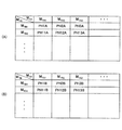
図18は、相互インダクタンスMTAと相互インダクタンスMTBとの関係に対して、位相を関連付けたテーブルデータを示す図である。FIG. 18 is a diagram illustrating table data in which phases are associated with the relationship between the mutual inductance MTA and the mutual inductance MTB .

図18の(A)は、調整部130Bを駆動する駆動信号の位相を0度に固定した状態で、調整部130Aを駆動する駆動信号の位相を調整するためのテーブルデータである。   FIG. 18A shows table data for adjusting the phase of the drive signal for driving the adjustment unit 130A in a state where the phase of the drive signal for driving the adjustment unit 130B is fixed at 0 degrees.

相互インダクタンスMTA1、MTA2、MTA3・・・は、実際には、具体的な相互インダクタンスMTAの値をとる。同様に、相互インダクタンスMTB1、MTB2、MTB3・・・は、実際には、具体的な相互インダクタンスMTBの値をとる。位相PH1A、PH2A、PH3A、・・・、PH11A、PH12A、PH13A、・・・は、具体的には、シミュレーションまたは実験的に求められた具体的な位相の値をとる。The mutual inductances M TA 1, M TA 2, M TA 3... Actually take a specific value of the mutual inductance M TA . Similarly, the mutual inductances M TB 1, M TB 2, M TB 3... Actually take a specific value of the mutual inductance M TB . Specifically, the phases PH1A, PH2A, PH3A,..., PH11A, PH12A, PH13A,... Take specific phase values obtained by simulation or experiment.

図18の(B)は、調整部130Aを駆動する駆動信号の位相を0度に固定した状態で、調整部130Bを駆動する駆動信号の位相を調整するためのテーブルデータである。   FIG. 18B shows table data for adjusting the phase of the drive signal for driving the adjustment unit 130B in a state where the phase of the drive signal for driving the adjustment unit 130A is fixed at 0 degrees.

相互インダクタンスMTA1、MTA2、MTA3・・・と、相互インダクタンスMTB1、MTB2、MTB3・・・は、図18の(A)と同様である。位相PH1B、PH2B、PH3B、・・・、PH11B、PH12B、PH13B、・・・は、具体的には、シミュレーションまたは実験的に求められた具体的な位相の値をとる。The mutual inductances M TA 1, M TA 2, M TA 3... And the mutual inductances M TB 1, M TB 2, M TB 3... Are the same as in FIG. Specifically, the phases PH1B, PH2B, PH3B,..., PH11B, PH12B, PH13B,... Take specific phase values obtained by simulation or experiment.

図18の(A)及び(B)に示すテーブルデータを実験的に求めるには、受電器100Aと100Bの送電器10に対する位置及び姿勢を様々に変えた状態で、相互インダクタンスMTAとMTBを計測しつつ、位相の最適化を図ることによって作成することができる。In order to experimentally obtain the table data shown in FIGS. 18A and 18B, the mutual inductances M TA and M TB are obtained with various positions and postures of the power receivers 100A and 100B with respect to the power transmitter 10. It can be created by optimizing the phase while measuring.

図19は、相互インダクタンスMTA、MTBと、受電効率とを関連付けたテーブルデータである。図19の(A)は、相互インダクタンスMTAと、受電器100Aの受電効率とを関連付けたテーブルデータであり、図19の(B)は、相互インダクタンスMTBと、受電器100Bの受電効率とを関連付けたテーブルデータである。FIG. 19 is table data in which mutual inductances M TA and M TB are associated with power reception efficiency. (A) of FIG. 19, the mutual inductance M TA, a table data that associates a power receiving efficiency of the power receiving device 100A, (B) of FIG. 19, the mutual inductance M TB, a power receiving efficiency of the power receiving device 100B Is table data associated with.

相互インダクタンスMTA、MTBは、それぞれ、送電装置80と、受電器100A、100Bとの受電効率E、Eによって決まる。The mutual inductances M TA and M TB are determined by power receiving efficiencies E A and E B between the power transmitting device 80 and the power receivers 100A and 100B, respectively.

図19の(A)では、相互インダクタンスMTA1、MTA2、・・・と、受電器100Aの受電効率EA1、EA2、・・・とが関連付けられている。また、図19の(B)では、相互インダクタンスMTB1、MTB2、・・・と、受電器100Bの受電効率EB1、EB2、・・・とが関連付けられている。In FIG. 19A, mutual inductances M TA 1, M TA 2,... Are associated with power receiving efficiencies E A1 , E A2,. In FIG. 19B, the mutual inductances M TB1 , M TB2 ,... Are associated with the power receiving efficiencies E B1 , E B2,.

予め実験等で受電器100A、100Bの相互インダクタンスMTA、MTBと、受電効率とを測定しておき、図19の(A)、(B)に示すようなテーブルデータを作成しておけば、受電器100A、100Bの受電効率から、受電器100A、100Bの相互インダクタンスMTA、MTBを求めることができる。あるいはシミュレーションによって、受電器100A、100Bの受電効率から、受電器100A、100Bの相互インダクタンスMTA、MTBを求めてもよい。If the mutual inductances M TA and M TB of the power receivers 100A and 100B and the power receiving efficiency are measured in advance through experiments or the like, table data as shown in FIGS. 19A and 19B is created. The mutual inductances M TA and M TB of the power receivers 100A and 100B can be obtained from the power reception efficiency of the power receivers 100A and 100B. Alternatively, the mutual inductances M TA and M TB of the power receivers 100A and 100B may be obtained from the power reception efficiency of the power receivers 100A and 100B by simulation.

次に、図20を用いて、位相の設定方法について説明する。   Next, a phase setting method will be described with reference to FIG.

図20は、実施の形態1の送電器10が受電器100A又は100Bの位相を設定する方法を示すフローチャートである。このフローは、送電器10の制御部15によって実行される処理を表し、図16のステップS3の処理内容の詳細を示すものである。   
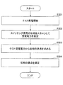
FIG. 20 is a flowchart illustrating a method in which the power transmitter 10 according to the first embodiment sets the phase of the power receiver 100A or 100B. This flow represents processing executed by the control unit 15 of the power transmitter 10, and shows details of the processing content of step S3 in FIG.

制御部15は、受電器100A及び100Bから受電電力を表す信号を受信して受電効率を求め、受電器100A及び100Bから定格出力を表す信号を受信してステップS3に進行すると、図20に示す処理を開始する。   When the control unit 15 receives the signal representing the received power from the power receivers 100A and 100B to obtain the power reception efficiency, receives the signal representing the rated output from the power receivers 100A and 100B, and proceeds to step S3, it is shown in FIG. Start processing.

制御部15は、バッテリ220Aの定格出力を二次側共振コイル110Aの受電効率で除算して得る第1の値と、バッテリ220Bの定格出力を二次側共振コイル110Bの受電効率で除算して得る第2の値とを求め、第1の値が第2の値よりも大きいか否かを判定する(ステップS31)。   The control unit 15 divides the rated output of the battery 220A by the power receiving efficiency of the secondary side resonance coil 110A and the first value obtained by dividing the rated output of the battery 220A by the power reception efficiency of the secondary side resonance coil 110B. A second value to be obtained is obtained, and it is determined whether or not the first value is larger than the second value (step S31).

制御部15は、第1の値が第2の値よりも大きい(S31:YES)と判定すると、受電器100Aの調整部130Aを駆動する駆動信号の位相を0度に設定する(ステップS31A)。位相を0度に設定するとは、位相の原点に設定することをいう。   When determining that the first value is larger than the second value (S31: YES), the control unit 15 sets the phase of the drive signal that drives the adjustment unit 130A of the power receiver 100A to 0 degrees (step S31A). . Setting the phase to 0 degrees means setting the phase origin.

なお、位相の原点は、位相シフト回路153で駆動信号の位相を変化させて、電圧計145の検出電圧に基づいて処理部151が算出する受電電力を検出することにより、図15に示す受電電力の最大値PMAXを与える位相θを求めればよい。The origin of the phase is obtained by changing the phase of the drive signal by the phase shift circuit 153 and detecting the received power calculated by the processing unit 151 based on the detected voltage of the voltmeter 145, thereby receiving the received power shown in FIG. it may be obtained the phase θ 0, which gives the maximum value P MAX of.

次いで、制御部15は、受電器100Bの調整部130Bを駆動する駆動信号の位相を設定する(ステップS32A)。具体的には、制御部15は、図14の(A)及び(B)に示すテーブルデータに基づき、それぞれ、受電器100A、100Bの受電効率E、Eから受電器100A、100Bの相互インダクタンスMTA、MTBを求める。そして、制御部15は、図13の(B)に示すテーブルデータから、受電器100A、100Bの相互インダクタンスMTA、MTBに基づいて、受電器100Bの調整部130Bを駆動する駆動信号の位相を求める。Next, the control unit 15 sets the phase of the drive signal that drives the adjustment unit 130B of the power receiver 100B (step S32A). Specifically, based on the table data shown in FIGS. 14A and 14B, the control unit 15 reciprocally receives the power reception efficiencies E A and E B of the power receivers 100A and 100B from the power receivers 100A and 100B. Inductances M TA and M TB are obtained. Then, the control unit 15 determines the phase of the drive signal that drives the adjustment unit 130B of the power receiver 100B based on the mutual inductances M TA and M TB of the power receivers 100A and 100B from the table data illustrated in FIG. Ask for.

ステップS32Aの処理が終了すると、制御部15はフローをステップS4(図11参照)に進行する。   When the process of step S32A ends, the control unit 15 advances the flow to step S4 (see FIG. 11).

また、制御部15は、第1の値が第2の値よりも小さい(S31:NO)と判定すると、受電器100Bの調整部130Bを駆動する駆動信号の位相を0度に設定する(ステップS31B)。位相を0度に設定するとは、位相の原点に設定することをいう。   If the control unit 15 determines that the first value is smaller than the second value (S31: NO), the control unit 15 sets the phase of the drive signal that drives the adjustment unit 130B of the power receiver 100B to 0 degrees (step S31). S31B). Setting the phase to 0 degrees means setting the phase origin.

次いで、制御部15は、受電器100Aの調整部130Aを駆動する駆動信号の位相を設定する(ステップS32B)。具体的には、制御部15は、図14の(A)及び(B)に示すテーブルデータに基づき、それぞれ、受電器100A、100Bの受電効率E、Eから受電器100A、100Bの相互インダクタンスMTA、MTBを求める。そして、制御部15は、図13の(A)に示すテーブルデータから、受電器100A、100Bの相互インダクタンスMTA、MTBに基づいて、受電器100Aの調整部130Aを駆動する駆動信号の位相を求める。Next, the control unit 15 sets the phase of the drive signal that drives the adjustment unit 130A of the power receiver 100A (step S32B). Specifically, based on the table data shown in FIGS. 14A and 14B, the control unit 15 reciprocally receives the power reception efficiencies E A and E B of the power receivers 100A and 100B from the power receivers 100A and 100B. Inductances M TA and M TB are obtained. Then, the control unit 15 determines the phase of the drive signal that drives the adjustment unit 130A of the power receiver 100A based on the mutual inductances M TA and M TB of the power receivers 100A and 100B from the table data illustrated in FIG. Ask for.

ステップS32Bの処理が終了すると、制御部15はフローをステップS4(図11参照)に進行する。   When the process of step S32B ends, the control unit 15 advances the flow to step S4 (see FIG. 11).

以上のようにして、制御部15は、受電器100A、100Bの調整部130A、130Bを駆動する駆動信号の位相を設定する。   As described above, the control unit 15 sets the phase of the drive signal that drives the adjustment units 130A and 130B of the power receivers 100A and 100B.

図21乃至図24は、制御部150が実行する処理を示すフローチャートである。   21 to 24 are flowcharts showing processing executed by the control unit 150.

ここでは、クロックCLK1、CLK2をスイッチ131X、131Yのスイッチングを行うスイッチング信号と称す。   Here, the clocks CLK1 and CLK2 are referred to as switching signals for switching the switches 131X and 131Y.

制御部150は、スイッチング信号の位相制御が必要であるかどうかを判定する(ステップS300)。スイッチング信号の位相制御が必要であるかどうかは、送電器10から受信する位相を調整する指令に含まれる第1指令と第2指令の内容によって決まる。   The controller 150 determines whether or not phase control of the switching signal is necessary (step S300). Whether or not the phase control of the switching signal is necessary depends on the contents of the first command and the second command included in the command for adjusting the phase received from the power transmitter 10.

第1指令が、電力の分配比を変更するために位相を調整することを表す場合は、スイッチング信号の位相制御が必要な場合である。また、第2指令がうなりに対する位相の調整を行うことを表す場合は、スイッチング信号の位相制御が必要な場合である。   When the first command indicates that the phase is adjusted in order to change the power distribution ratio, the phase control of the switching signal is necessary. In addition, when the second command indicates that the phase is adjusted with respect to the beat, the phase control of the switching signal is necessary.

スイッチング信号の位相制御が必要ではない場合は、第1指令が、電力の分配比を変更するための位相の調整を行わないことを表し、かつ、第2指令がうなりに対する位相の調整を行わないことを表す場合である。   When the phase control of the switching signal is not necessary, the first command indicates that the phase adjustment for changing the power distribution ratio is not performed, and the second command does not adjust the phase for the beat. This is the case.

制御部150は、スイッチング信号の位相制御が必要である(S300:YES)と判定すると、スイッチング信号の周波数を調整する(ステップS310)。ステップS310の詳細は、図22を用いて後述するが、ステップS310では、制御部150は、経過時間tが過渡応答期間tよりも十分に長くなるように、クロックCLK1、CLK2の周波数を調整する。When determining that the phase control of the switching signal is necessary (S300: YES), the controller 150 adjusts the frequency of the switching signal (step S310). Details of step S310, the will be described later with reference to FIG. 22, in step S310, the control unit 150, as the elapsed time t X is sufficiently longer than the transient response period t P, the frequency of the clock CLK1, CLK2 adjust.

制御部150は、位相の原点を求める(ステップS320)。ステップS320の詳細は、図23を用いて後述するが、ステップS320では、制御部150は、図15を用いて説明したように、位相の原点を求める。   The control unit 150 obtains the origin of the phase (Step S320). Details of step S320 will be described later with reference to FIG. 23. In step S320, the control unit 150 obtains the phase origin as described with reference to FIG.

制御部150は、受電器100(自己)が移動しているかどうかを判定する(ステップS330)。受電器100(自己)が移動しているかどうかは、例えば、制御部150を含む電子機器が内蔵する加速度センサ41(図4参照)の検出値に基づいて判定すればよい。   The controller 150 determines whether or not the power receiver 100 (self) is moving (step S330). Whether or not the power receiver 100 (self) is moving may be determined based on, for example, a detection value of the acceleration sensor 41 (see FIG. 4) built in the electronic device including the control unit 150.

ステップS330で受電器100(自己)が移動しているかどうかを判定するのは、受電電力の低下が、制御部150が送電器10から離れていることが原因なのか、受電電力のうなりによる低下であるのかを切り分けて処理を行うためである。   In step S330, whether the power receiver 100 (self) is moving is determined because the decrease in the received power is caused by the control unit 150 being away from the power transmitter 10, or the decrease in the received power due to the beat. This is because the process is performed by categorizing whether it is.

制御部150は、受電器100(自己)が移動していない(S330:NO)と判定すると、スイッチング信号の位相を制御する(ステップS340)。ステップS340の詳細は、図24を用いて後述するが、ステップS340では、制御部150は、スイッチング信号の位相を制御することにより、うなりによって低下している受電電力を増大させる。   When determining that the power receiver 100 (self) is not moving (S330: NO), the control unit 150 controls the phase of the switching signal (step S340). The details of step S340 will be described later with reference to FIG. 24. In step S340, the control unit 150 controls the phase of the switching signal to increase the received power that is reduced due to the beat.

制御部150は、受電状態が継続しているかどうかを判定する(ステップS350)。ステップS350では、受電器100(自己)が受電しているかどうかで判定すればよい。   The control unit 150 determines whether or not the power receiving state continues (step S350). In step S350, it may be determined whether the power receiver 100 (self) is receiving power.

制御部150は、受電状態が継続している(S350:YES)と判定すると、フローをステップS340にリターンする。この結果、制御部150は、スイッチング信号の位相を制御することにより、うなりによって低下している受電電力を増大させる。   If the control unit 150 determines that the power receiving state continues (S350: YES), the control unit 150 returns the flow to step S340. As a result, the control unit 150 controls the phase of the switching signal to increase the received power that is reduced due to the beat.

また、制御部150は、受電状態が継続していない(S350:NO)と判定すると、一連の処理を終了する(エンド)。   If control unit 150 determines that the power receiving state does not continue (S350: NO), it ends the series of processes (end).

制御部150は、受電器100(自己)が移動している(S330:YES)と判定すると、受電電力が減少しているかどうかを判定する(ステップS351)。   When determining that the power receiver 100 (self) is moving (S330: YES), the controller 150 determines whether the received power is decreasing (step S351).

制御部150は、受電電力が減少している(S351:YES)と判定すると、スイッチング信号の位相は最大値θMAXであるかどうかを判定する(ステップS352)。受電電力が減少しているかどうかは、電圧計145の検出電圧に基づいて処理部151が算出する受電電力が減少しているかどうかで判定すればよい。If controller 150 determines that the received power is decreasing (S351: YES), controller 150 determines whether the phase of the switching signal is maximum value θ MAX (step S352). Whether or not the received power is decreasing may be determined by whether or not the received power calculated by the processing unit 151 is decreasing based on the detection voltage of the voltmeter 145.

最大値θMAXとは、スイッチング信号の位相の調整幅の最大値である。すなわち、ステップS352は、スイッチング信号の位相をさらに調整できるかどうかを判定するステップである。最大値θMAXは、360度である。The maximum value θ MAX is the maximum value of the adjustment range of the phase of the switching signal. That is, step S352 is a step of determining whether or not the phase of the switching signal can be further adjusted. The maximum value θ MAX is 360 degrees.

ステップS352に辿り着く場合は、受電電力が減少していて、これ以上、スイッチング信号の位相を調整する余裕がない状態である。このような場合には、送電器10の送電電力を増大させる。   When the process reaches step S352, the received power is reduced and there is no more room for adjusting the phase of the switching signal. In such a case, the transmission power of the power transmitter 10 is increased.

制御部150は、スイッチング信号の位相が最大値θMAXである(S352:YES)と判定すると、送電電力を増大させる指令を送電器10に送信する(ステップS353)。制御部150は、送電電力を増大させる指令を無線通信で送電器10に送信する。この処理は処理部151が実行する。When determining that the phase of the switching signal is the maximum value θ MAX (S352: YES), control unit 150 transmits a command to increase the transmitted power to power transmitter 10 (step S353). The control unit 150 transmits a command to increase the transmitted power to the power transmitter 10 by wireless communication. This processing is executed by the processing unit 151.

制御部150は、受電状態が継続しているかどうかを判定する(ステップS354)。ステップS354では、受電器100(自己)が受電しているかどうかで判定すればよい。   The control unit 150 determines whether or not the power receiving state continues (step S354). In step S354, the determination may be made based on whether the power receiver 100 (self) is receiving power.

制御部150は、受電状態が継続していない(S354:NO)と判定すると、一連の処理を終了する(エンド)。   If control unit 150 determines that the power receiving state does not continue (S354: NO), it ends the series of processes (end).

制御部150は、受電状態が継続している(S354:YES)と判定すると、スイッチング信号の位相制御を継続するかどうかを判定する(ステップS358)。位相制御を継続するかどうかは、送電器10から受信する位相を調整する指令に含まれる第1指令と第2指令の内容によって決まる。   When determining that the power receiving state is continued (S354: YES), control unit 150 determines whether or not to continue the phase control of the switching signal (step S358). Whether to continue the phase control depends on the contents of the first command and the second command included in the command for adjusting the phase received from the power transmitter 10.

また、制御部150は、ステップS351において、受電電力が減少していない(S351:NO)と判定すると、スイッチング信号の位相を調整して受電電力を減少させる(ステップS355)。受電器100(自己)が移動して受電電力が増大している場合は、受電器100(自己)が送電器10に近づいている場合であるため、受電量を減らすこととしたものである。   If controller 150 determines in step S351 that received power has not decreased (S351: NO), controller 150 adjusts the phase of the switching signal to decrease received power (step S355). When the power receiver 100 (self) moves and the received power is increased, the power receiver 100 (self) is approaching the power transmitter 10, and thus the amount of power received is reduced.

制御部150は、ステップS351の処理を終えると、フローをステップS300にリターンする。   When the process of step S351 is completed, the control unit 150 returns the flow to step S300.

また、制御部150は、ステップS352において、スイッチング信号の位相が最大値θMAXではない(S352:NO)と判定すると、スイッチング信号の位相を調整して受電電力を増大させる(ステップS356)。受電器100(自己)が移動して受電電力が減少している場合は、受電器100(自己)が送電器10から遠ざかっている場合であるため、受電量を増大することとしたものである。If controller 150 determines in step S352 that the phase of the switching signal is not the maximum value θ MAX (S352: NO), controller 150 adjusts the phase of the switching signal to increase the received power (step S356). When the power receiver 100 (self) moves and the received power is reduced, the power receiver 100 (self) is moving away from the power transmitter 10, and thus the amount of power received is increased. .

制御部150は、ステップS356の処理を終えると、設定した受電電力(設定受電電力)に到達しているかどうかを判定する(ステップS357)。設定した受電電力とは、第1指令によって決まる電力である。ステップS357の処理は、電圧計145の検出電圧に基づいて処理部151が算出する受電電力が第1指令によって決まる電力に達成したかどうかを処理部151が判定することによって行われる。   After finishing the process of step S356, the controller 150 determines whether or not the set received power (set received power) has been reached (step S357). The set received power is power determined by the first command. The processing in step S357 is performed by the processing unit 151 determining whether the received power calculated by the processing unit 151 based on the detected voltage of the voltmeter 145 has reached the power determined by the first command.

制御部150は、設定した受電電力に到達している(S357:YES)と判定すると、フローをステップS300にリターンする。   If the control unit 150 determines that the set received power has been reached (S357: YES), the control unit 150 returns the flow to step S300.

また、制御部150は、設定した受電電力に到達していない(S357:NO)と判定すると、フローをステップS353に進行させる。   Further, when determining that the set received power has not been reached (S357: NO), control unit 150 causes the flow to proceed to step S353.

また、制御部150は、スイッチング信号の位相制御が必要ではない(S300:NO)と判定すると、位相を0度(位相の原点)に調整する(ステップS359)。ステップS359の処理が終了すると、一連の処理が終了する(エンド)。   If controller 150 determines that phase control of the switching signal is not necessary (S300: NO), controller 150 adjusts the phase to 0 degrees (phase origin) (step S359). When the process of step S359 ends, a series of processes ends (end).

以上で、図21に示すフローが終了する。   Thus, the flow shown in FIG. 21 ends.

次に、図22に示すフローチャートについて説明する。   Next, the flowchart shown in FIG. 22 will be described.

制御部150は、テスト受電を開始する(ステップS311)。テスト受電は、予め設定した所定電力を送電器10に送電させて、受電状態をテストするものである。ここでは、受電電力にうなりがあるかどうかを判定できればよいため、予め設定した所定電力は、非常に少ない電力でよい。   The control unit 150 starts test power reception (step S311). In the test power reception, a predetermined power set in advance is transmitted to the power transmitter 10 to test the power reception state. Here, since it is only necessary to determine whether the received power is beaten, the predetermined power set in advance may be very small.

制御部150は、受電電力のうなりが所定レベル以下であるかどうかを判定する(ステップS312)。所定レベル以下であるかどうかは、例えば、時間変化に対するうなりの減少度合が所定値以下であって十分に小さく、うなりの周波数が十分に低いかどうかで判定すればよい。   The control unit 150 determines whether or not the beat of the received power is below a predetermined level (step S312). Whether or not the level is below a predetermined level may be determined, for example, based on whether or not the rate of decrease of the beat with respect to the time change is not more than a predetermined value and is sufficiently small, and the beat frequency is sufficiently low.

制御部150は、受電電力のうなりが所定レベル以下である(S312:YES)と判定すると、スイッチング信号の周波数を調整する(ステップS313)。ステップS313では、制御部150は、経過時間tが過渡応答期間tよりも十分に長くなるように、クロックCLK1、CLK2の周波数を調整する。If controller 150 determines that the beat of received power is below a predetermined level (S312: YES), controller 150 adjusts the frequency of the switching signal (step S313). In step S313, the control unit 150, the elapsed time t X is to be sufficiently longer than the transient response period t P, adjusting the frequency of the clock CLK1, CLK2.

制御部150は、ステップS313の処理を終えると、フローをステップS312にリターンする。   When the process of step S313 is completed, the control unit 150 returns the flow to step S312.

制御部150は、受電電力のうなりが所定レベル以下ではない(S312:NO)と判定すると、スイッチング信号の周波数をそのときの値に設定する(ステップS314)。   When determining that the beat of the received power is not equal to or lower than the predetermined level (S312: NO), control unit 150 sets the frequency of the switching signal to the value at that time (step S314).

以上で、スイッチング信号の周波数を調整するステップS310が完了する(エンド)。   Thus, step S310 for adjusting the frequency of the switching signal is completed (END).

次に、図23に示すフローチャートについて説明する。   Next, the flowchart shown in FIG. 23 will be described.

制御部150は、テスト受電を開始する(ステップS321)。テスト受電は、予め設定した所定電力を送電器10に送電させて、受電状態をテストするものである。ここでは、受電電力にうなりがあるかどうかを判定できればよいため、予め設定した所定電力は、非常に少ない電力でよい。   The control unit 150 starts test power reception (step S321). In the test power reception, a predetermined power set in advance is transmitted to the power transmitter 10 to test the power reception state. Here, since it is only necessary to determine whether the received power is beaten, the predetermined power set in advance may be very small.

制御部150は、スイッチング信号の位相をスキャンして受電電力を測定する(ステップS322)。スイッチング信号の位相をスキャンするには、位相シフト回路153でスイッチング信号の位相をシフトすればよく、360度シフトさせながら、電圧計145の検出電圧に基づいて処理部151が受電電力を測定すればよい。これにより、図15に示すような特性が求められる。   The control unit 150 scans the phase of the switching signal and measures received power (step S322). In order to scan the phase of the switching signal, the phase of the switching signal may be shifted by the phase shift circuit 153. If the processing unit 151 measures the received power based on the detected voltage of the voltmeter 145 while shifting it by 360 degrees. Good. Thereby, characteristics as shown in FIG. 15 are obtained.

制御部150は、ステップS322で得た特性から、受電電力が最大値になる位相を位相の原点として求める(ステップS323)。   From the characteristics obtained in step S322, control unit 150 obtains the phase at which the received power is maximum as the phase origin (step S323).

制御部150は、ステップS323で得た位相の原点をスイッチング信号に設定する(ステップS323)。具体的には、位相制御部154が位相の原点を表す値を保持し、位相シフト回路153に設定すればよい。   The controller 150 sets the origin of the phase obtained in step S323 as a switching signal (step S323). Specifically, the phase control unit 154 may hold a value indicating the origin of the phase and set it in the phase shift circuit 153.

以上で、位相の原点を求めるステップS320の処理が完了する(エンド)。   This completes the processing of step S320 for obtaining the phase origin (end).

次に、図24に示すフローチャートについて説明する。   Next, the flowchart shown in FIG. 24 will be described.

制御部150は、本送電が開始したかどうかを判定する(ステップS331)。本送電が開始したかどうかは、例えば、送電器10から本送電を開始することを表す通知信号を受信したかどうかで判定すればよい。   The control unit 150 determines whether the main power transmission has started (step S331). Whether or not the main power transmission has started may be determined based on whether or not a notification signal representing the start of the main power transmission is received from the power transmitter 10, for example.

制御部150は、処理部151が算出する受電電力Pと設定受電電力Psとの誤差ΔPを検出する(ステップS342)。設定受電電力Psとは、ステップS357の設定受電電力と同一である。誤差ΔPは、設定受電電力Psから受電電力Pを減算することによって得られる。   The control unit 150 detects an error ΔP between the received power P calculated by the processing unit 151 and the set received power Ps (step S342). The set received power Ps is the same as the set received power in step S357. The error ΔP is obtained by subtracting the received power P from the set received power Ps.

制御部150は、誤差ΔPが閾値以上であるかどうかを判定する(ステップS343)。   The control unit 150 determines whether or not the error ΔP is greater than or equal to a threshold value (step S343).

制御部150は、誤差ΔPが閾値以上である(S343:YES)と判定すると、スイッチング信号の位相を調整する(ステップS344)。   If controller 150 determines that error ΔP is greater than or equal to the threshold (S343: YES), controller 150 adjusts the phase of the switching signal (step S344).

制御部150は、調整前の動作状態における位相が図8の横軸に示す位相が正の領域にある場合には、受電電力を増大させるために位相を小さくすればよい。例えば、調整前の位相が30度である場合には、30度よりも0度に近づけて、位相を小さくすればよい。   When the phase in the operating state before adjustment is in the positive region, the control unit 150 may reduce the phase in order to increase the received power. For example, when the pre-adjustment phase is 30 degrees, the phase may be made closer to 0 degrees than 30 degrees.

制御部150は、調整前の動作状態における位相が図8の横軸に示す位相が負の領域にある場合には、受電電力を増大させるために位相を大きくすればよい。例えば、調整前の位相が−30度である場合には、−30度よりも0度に近づけて、位相を大きくすればよい。   When the phase in the operation state before adjustment is in the negative region, the control unit 150 may increase the phase in order to increase the received power. For example, when the phase before adjustment is −30 degrees, the phase may be increased closer to 0 degrees than −30 degrees.

制御部150は、誤差ΔPが閾値以上ではない(S343:NO)と判定すると、送電終了であるかどうかを判定する(ステップS345)。送電終了であるかどうかは、例えば、受電器100が送電器10から送電終了であることを表す信号を受信したかどうかで判断すればよい。   If controller 150 determines that error ΔP is not greater than or equal to the threshold (S343: NO), controller 150 determines whether or not power transmission is complete (step S345). Whether or not power transmission has ended may be determined, for example, by whether or not the power receiver 100 has received a signal indicating that power transmission has ended from the power transmitter 10.

以上、実施の形態1によれば、受電器100A及び100Bの二次側共振コイル110A及び110Bの受電効率と、電子機器200A及び200Bの定格出力とにより、受電器100A及び100Bへの必要送電量を求める。   As described above, according to the first embodiment, the necessary power transmission amount to the power receivers 100A and 100B based on the power reception efficiency of the secondary resonance coils 110A and 110B of the power receivers 100A and 100B and the rated output of the electronic devices 200A and 200B. Ask for.

そして、受電器100A及び100Bのうち、必要送電量が小さい方の受電器(100A又は100B)に対応する駆動信号の位相を位相の原点から変化させる。   Then, the phase of the drive signal corresponding to the power receiver (100A or 100B) having the smaller required power transmission amount among the power receivers 100A and 100B is changed from the phase origin.

この結果、必要送電量が小さい方の受電器(100A又は100B)への電力供給量が絞られ、必要送電量が大きい方の受電器(100A又は100B)への電力供給量を増やすことができる。   As a result, the power supply amount to the power receiver (100A or 100B) having the smaller required power transmission amount can be reduced, and the power supply amount to the power receiver (100A or 100B) having the larger necessary power transmission amount can be increased. .

このようにして、受電器100A及び100Bへの電力供給量のバランスを改善する。   In this way, the balance of the amount of power supplied to the power receivers 100A and 100B is improved.

従って、実施の形態1によれば、電力供給量のバランスを改善することのできる受電器100A又は100Bを提供することができる。また、実施の形態1によれば、電力供給量のバランスを改善することができる電力伝送システム400を提供することができる。   Therefore, according to Embodiment 1, the power receiver 100A or 100B that can improve the balance of the power supply amount can be provided. Moreover, according to Embodiment 1, the electric power transmission system 400 which can improve the balance of the electric power supply amount can be provided.

また、実施の形態1によれば、受電電力がX%低下するまでの経過時間tが、クロックCLK1、CLK2の位相を調整してから受電電力が安定するまでの過渡応答期間tよりも十分に長くなるようにクロックCLK1、CLK2の周波数を調整する。Further, according to the first embodiment, the elapsed time t X until received power drops X% is the clock CLK1, the reception power after adjusting the phase of the CLK2 than the transient response period t P to stabilize The frequencies of the clocks CLK1 and CLK2 are adjusted so as to be sufficiently long.

このため、うなりの周期による受電電力の変化を緩和することができ、受電電力の急激な変化を抑制することができる。   For this reason, the change in the received power due to the beat period can be alleviated, and a rapid change in the received power can be suppressed.

また、実施の形態1によれば、受電電力のうなりによって誤差ΔPが大きくなると、クロックCLK1、CLK2(スイッチング信号)の位相を調整して受電電力を増大させる。このため、うなりによる受電電力の低下を抑制することができ、効率的に受電することができる。   Further, according to the first embodiment, when the error ΔP increases due to the beat of the received power, the received power is increased by adjusting the phases of the clocks CLK1 and CLK2 (switching signals). For this reason, the fall of the received electric power by a beating can be suppressed, and it can receive electric power efficiently.

また、以上では、位相の原点を求めて、位相の原点からクロックCLK1、CLK2(スイッチング信号)の位相を変化させる形態について説明した。しかしながら、位相の原点を求めずに、クロックCLK1、CLK2(スイッチング信号)の位相を変化させてもよい。この場合には、図18及び図19に示すデータを用いる必要はない。   In the above description, the phase origin is obtained and the phases of the clocks CLK1 and CLK2 (switching signals) are changed from the phase origin. However, the phases of the clocks CLK1 and CLK2 (switching signals) may be changed without obtaining the phase origin. In this case, it is not necessary to use the data shown in FIGS.

位相の原点を求めずに、クロックCLK1、CLK2(スイッチング信号)の位相を変化させる場合は、例えば、実験等で、位相と受電電力の関係を予め調べた上で設定すればよい。また、位相を進めるか遅延させるかについても、位相と受電電力の関係を予め調べた上で設定すればよい。   When the phases of the clocks CLK1 and CLK2 (switching signals) are changed without obtaining the phase origin, for example, the relationship between the phase and the received power may be set in advance through an experiment or the like. Further, whether to advance or delay the phase may be set after examining the relationship between the phase and the received power in advance.

また、以上では、2つの受電器100A及び100Bのうち、必要送電量が小さい方の受電器(100A又は100B)に対応する駆動信号の位相を低減することによって受電器100A及び100Bへの電力供給量のバランスを改善する形態について説明した。   In the above, power supply to the power receivers 100A and 100B is achieved by reducing the phase of the drive signal corresponding to the power receiver (100A or 100B) having the smaller required power transmission amount of the two power receivers 100A and 100B. A mode of improving the balance of the amount has been described.

しかしながら、3つ以上の受電器が同時に充電される場合もある。このような場合には、必要電力量、つまりは各定格電力を各受電効率で除算して得る電力量が最大の受電器以外の受電器の駆動信号の位相を低減するようにすればよい。   However, more than two power receivers may be charged at the same time. In such a case, the phase of the drive signal of the power receiver other than the power receiver having the maximum power amount obtained by dividing the required power amount, that is, each rated power by each power receiving efficiency, may be reduced.

また、以上では、電子機器200A及び200Bが、一例として、タブレットコンピュータ又はスマートフォン等の端末機である形態について説明したが、電子機器200A及び200Bは、例えば、ノート型のPC(Personal Computer)、携帯電話端末機、携帯型のゲーム機、デジタルカメラ、ビデオカメラ等の充電式のバッテリを内蔵する電子機器であってもよい。   In the above description, the electronic devices 200A and 200B are described as an example of a terminal such as a tablet computer or a smartphone. However, the electronic devices 200A and 200B are, for example, a notebook PC (Personal Computer), a mobile phone, and the like. An electronic device incorporating a rechargeable battery such as a telephone terminal, a portable game machine, a digital camera, or a video camera may be used.

また、以上では、2つの受電器100A及び100Bの受電効率と定格出力に応じて位相を求め、制御部150A又は150Bがスイッチ131A及び131Bを駆動する駆動信号の位相を調整する形態について説明した。   In the above description, the phase is determined according to the power reception efficiency and the rated output of the two power receivers 100A and 100B, and the control unit 150A or 150B adjusts the phase of the drive signal that drives the switches 131A and 131B.

しかしながら、1つの送電器10と1つの受電器100(図4参照)との間で電力を伝送する場合には、受電器100の制御部150が、実験等で予め求めておいた位相を用いてスイッチ131A及び131Bを駆動してもよい。この場合には、制御部150の内部メモリにバッテリ220の定格出力を表すデータを格納しておく必要はない。   However, when power is transmitted between one power transmitter 10 and one power receiver 100 (see FIG. 4), the control unit 150 of the power receiver 100 uses a phase that has been obtained in advance through experiments or the like. The switches 131A and 131B may be driven. In this case, it is not necessary to store data representing the rated output of the battery 220 in the internal memory of the control unit 150.

また、1つの送電器10と1つの受電器100(図4参照)との間で電力を伝送する場合には、受電器100の制御部150がクロックCLK1、CLK2の位相を調整することによって、受電電力を調整することができる。この場合には、受電器100が受電する電力が最大になる位相を検出する必要はない。   Further, when power is transmitted between one power transmitter 10 and one power receiver 100 (see FIG. 4), the control unit 150 of the power receiver 100 adjusts the phases of the clocks CLK1 and CLK2, The received power can be adjusted. In this case, it is not necessary to detect the phase at which the power received by the power receiver 100 is maximized.

また、以上では、受電器100A及び100Bがバッテリ220A及び220Bを同時に充電する形態について説明した。しかしながら、電子機器200A及び200Bは、バッテリ220A及び220Bを含まずに、受電器100A及び100Bが受電した電力を直接的に消費して動作してもよい。受電器100A及び100Bは、同時に効率的に受電できるので、電子機器200A及び200Bがバッテリ220A及び220Bを含まない場合でも、電子機器200A及び200Bが同時に駆動することが可能になる。これは、時分割的に受電する場合には不可能であるため、同時に受電する場合のメリットの一つである。なお、このような場合には、電子機器200A及び200Bの駆動に必要な定格出力を用いて、位相を設定すればよい。   In the above description, the power receivers 100A and 100B charge the batteries 220A and 220B at the same time. However, the electronic devices 200A and 200B may operate by directly consuming the power received by the power receivers 100A and 100B without including the batteries 220A and 220B. Since the power receivers 100A and 100B can receive power efficiently at the same time, even when the electronic devices 200A and 200B do not include the batteries 220A and 220B, the electronic devices 200A and 200B can be driven simultaneously. This is impossible when receiving power in a time-sharing manner, and is one of the merits when receiving power simultaneously. In such a case, the phase may be set using the rated output necessary for driving the electronic devices 200A and 200B.

また、以上では、送電器10の制御部15が駆動信号を生成し、受電器100A及び100Bに送信する形態について説明したが、送電器10の送電電力を表すデータを受電器100A、100Bに送信し、受電器100A、100B側で駆動信号を生成してもよい。この場合に、受電器100Aと100Bとの間でデータ通信を行い、受電器100A又は100Bで、どちらの受電電力が大きいかを判定し、受電電力の少ない方の受電器(100A又は100B)の駆動信号の位相を増大するように、少なくともいずれか一方の受電器(100A又は100B)が駆動信号を生成するようにすればよい。   In the above description, the control unit 15 of the power transmitter 10 generates a drive signal and transmits the drive signal to the power receivers 100A and 100B. However, data representing the transmitted power of the power transmitter 10 is transmitted to the power receivers 100A and 100B. Then, a drive signal may be generated on the power receivers 100A and 100B side. In this case, data communication is performed between the power receivers 100A and 100B, the power receiver 100A or 100B determines which received power is larger, and the power receiver (100A or 100B) with the smaller received power is used. It is sufficient that at least one of the power receivers (100A or 100B) generates the drive signal so as to increase the phase of the drive signal.

また、送電器10が受電器100A、100Bから受電電力と定格出力を表すデータを受信して、必要送電量が小さい方の受電器(100A又は100B)の制御部(150A又は150B)に位相を調整させるようにしてもよい。この場合に、位相を調整するために必要なデータは、制御部(150A又は150B)が内部メモリに格納すればよい。   In addition, the power transmitter 10 receives the data indicating the received power and the rated output from the power receivers 100A and 100B, and sets the phase to the control unit (150A or 150B) of the power receiver (100A or 100B) having the smaller required power transmission amount. You may make it adjust. In this case, data necessary for adjusting the phase may be stored in the internal memory by the control unit (150A or 150B).

また、調整部130のダイオード131X及び131Yの向きは、図4に示す向きとは反対であってもよい。図25は、実施の形態1の変形例の調整部130Vを示す図である。   Further, the direction of the diodes 131X and 131Y of the adjustment unit 130 may be opposite to the direction shown in FIG. FIG. 25 is a diagram illustrating an adjustment unit 130 </ b> V according to a modification of the first embodiment.

調整部130Vは、スイッチ131X、131Y、ダイオード132VX、132VY、キャパシタ133X、133Y、及び端子134X、134Yを有する。ダイオード132VX、132VYの整流方向は、それぞれ、図4に示すダイオード132X、132Yと反対である。それ以外は、図4に示す調整部130と同様であるため、同様の構成要素には同一符号を付し、その説明を省略する。   The adjustment unit 130V includes switches 131X and 131Y, diodes 132VX and 132VY, capacitors 133X and 133Y, and terminals 134X and 134Y. The rectification directions of the diodes 132VX and 132VY are opposite to those of the diodes 132X and 132Y shown in FIG. Other than that, the configuration is the same as that of the adjusting unit 130 shown in FIG.

図26は、キャパシタ115及び調整部130Vにおける電流経路を示す図である。図26では、端子134Xからキャパシタ115又は調整部130Vの内部を通って端子134Yに流れる電流の向きを時計回り(CW(Clockwise))と称す。また、端子134Yからキャパシタ115又は調整部130Vの内部を通って端子134Xに流れる電流の向きを反時計回り(CCW(Counterclockwise))と称す。   FIG. 26 is a diagram illustrating a current path in the capacitor 115 and the adjustment unit 130V. In FIG. 26, the direction of current flowing from the terminal 134X through the capacitor 115 or the adjustment unit 130V to the terminal 134Y is referred to as clockwise (CW (Clockwise)). The direction of current flowing from the terminal 134Y through the capacitor 115 or the adjustment unit 130V to the terminal 134X is referred to as counterclockwise (CCW (Counterclockwise)).

スイッチ131Xがオフでスイッチ131Yがオンで、電流が時計回り(CW)の場合は、調整部130V内では端子134Xからダイオード132VX及びスイッチ131Yを経て端子134Yに向かう電流経路が生じる。この電流経路は、キャパシタ115に並列であるため、キャパシタ115には電流が流れなくなる。従って、二次側共振コイル110には共振電流は流れない。   When the switch 131X is off and the switch 131Y is on and the current is clockwise (CW), a current path from the terminal 134X to the terminal 134Y through the diode 132VX and the switch 131Y is generated in the adjustment unit 130V. Since this current path is parallel to the capacitor 115, no current flows through the capacitor 115. Therefore, no resonance current flows through the secondary resonance coil 110.

スイッチ131Xがオフでスイッチ131Yがオンで、電流が反時計回り(CCW)の場合は、調整部130V内では端子134Yからスイッチ131Y及びキャパシタ133Xを経て端子134Xに向かう方向に共振電流が流れるとともに、キャパシタ115には端子115Yから端子115Xに共振電流が流れる。従って、二次側共振コイル110には反時計回りの方向に共振電流が流れる。   When the switch 131X is off and the switch 131Y is on and the current is counterclockwise (CCW), a resonance current flows from the terminal 134Y to the terminal 134X through the switch 131Y and the capacitor 133X in the adjustment unit 130V. In the capacitor 115, a resonance current flows from the terminal 115Y to the terminal 115X. Therefore, a resonance current flows in the secondary side resonance coil 110 in the counterclockwise direction.

スイッチ131Xがオンでスイッチ131Yがオフで、電流が時計回り(CW)の場合は、調整部130V内では端子134Xからスイッチ131X及びキャパシタ133Yを経て端子134Yに向かう方向に共振電流が流れるとともに、キャパシタ115には端子115Xから端子115Yに共振電流が流れる。従って、二次側共振コイル110には時計回りの方向に共振電流が流れる。   When the switch 131X is on, the switch 131Y is off, and the current is clockwise (CW), a resonance current flows from the terminal 134X to the terminal 134Y through the switch 131X and the capacitor 133Y in the adjustment unit 130V. In 115, a resonance current flows from the terminal 115X to the terminal 115Y. Accordingly, a resonance current flows through the secondary side resonance coil 110 in the clockwise direction.

スイッチ131Xがオンでスイッチ131Yがオフで、電流が反時計回り(CCW)の場合は、調整部130V内では端子134Yからダイオード132VY及びスイッチ131Xを経て端子134Xに向かう電流経路が生じる。この電流経路は、キャパシタ115に並列であるため、キャパシタ115には電流が流れなくなる。従って、二次側共振コイル110には共振電流は流れない。   When the switch 131X is on, the switch 131Y is off, and the current is counterclockwise (CCW), a current path from the terminal 134Y to the terminal 134X through the diode 132VY and the switch 131X is generated in the adjustment unit 130V. Since this current path is parallel to the capacitor 115, no current flows through the capacitor 115. Therefore, no resonance current flows through the secondary resonance coil 110.

<実施の形態2>
図27は、実施の形態2の受電器500と送電装置80を示す図である。送電装置80は、交流電源1と送電器10を含む。以下では、実施の形態1の構成要素と同様の構成要素には同一符号を付し、その説明を省略する。
<Embodiment 2>
FIG. 27 is a diagram illustrating the power receiver 500 and the power transmission device 80 according to the second embodiment. The power transmission device 80 includes an AC power source 1 and a power transmitter 10. Below, the same code | symbol is attached | subjected to the component similar to the component of Embodiment 1, and the description is abbreviate | omitted.

送電装置80は、交流電源1と送電器10を含む。   The power transmission device 80 includes an AC power source 1 and a power transmitter 10.

送電器10は、一次側コイル11、一次側共振コイル12、整合回路13、キャパシタ14、制御部15、及びアンテナ16を有する。   The power transmitter 10 includes a primary side coil 11, a primary side resonance coil 12, a matching circuit 13, a capacitor 14, a control unit 15, and an antenna 16.

受電器500は、二次側共振コイル110、キャパシタ115、整流回路120、調整部530、平滑キャパシタ140、制御部150、電圧計160V、出力端子160X、160Y、及びアンテナ170を含む。出力端子160X、160Yには、DC−DCコンバータ210が接続されており、DC−DCコンバータ210の出力側にはバッテリ220が接続されている。   The power receiver 500 includes a secondary side resonance coil 110, a capacitor 115, a rectifier circuit 120, an adjustment unit 530, a smoothing capacitor 140, a control unit 150, a voltmeter 160V, output terminals 160X and 160Y, and an antenna 170. A DC-DC converter 210 is connected to the output terminals 160X and 160Y, and a battery 220 is connected to the output side of the DC-DC converter 210.

まず、送電器10について説明する。図27に示すように、一次側コイル11は、ループ状のコイルであり、両端間に整合回路13を介して交流電源1に接続されている。一次側コイル11は、一次側共振コイル12と非接触で近接して配置されており、一次側共振コイル12と電磁界結合される。一次側コイル11は、自己の中心軸が一次側共振コイル12の中心軸と一致するように配設される。中心軸を一致させるのは、一次側コイル11と一次側共振コイル12との結合強度を向上させるとともに、磁束の漏れを抑制して、不必要な電磁界が一次側コイル11及び一次側共振コイル12の周囲に発生することを抑制するためである。   First, the power transmitter 10 will be described. As shown in FIG. 27, the primary side coil 11 is a loop-shaped coil, and is connected to the AC power source 1 via the matching circuit 13 between both ends. The primary side coil 11 is disposed in close proximity to the primary side resonance coil 12 and is electromagnetically coupled to the primary side resonance coil 12. The primary coil 11 is disposed so that its central axis coincides with the central axis of the primary resonance coil 12. Matching the central axes improves the coupling strength between the primary side coil 11 and the primary side resonance coil 12 and suppresses leakage of magnetic flux, so that unnecessary electromagnetic fields are generated by the primary side coil 11 and the primary side resonance coil. This is to suppress the occurrence of the noise around 12.

一次側コイル11は、交流電源1から整合回路13を経て供給される交流電力によって磁界を発生し、電磁誘導(相互誘導)により電力を一次側共振コイル12に送電する。   The primary coil 11 generates a magnetic field by AC power supplied from the AC power supply 1 through the matching circuit 13 and transmits the power to the primary resonance coil 12 by electromagnetic induction (mutual induction).

図27に示すように、一次側共振コイル12は、一次側コイル11と非接触で近接して配置されて一次側コイル11と電磁界結合されている。また、一次側共振コイル12は、所定の共振周波数を有し、高いQ値を有するように設計されている。一次側共振コイル12の共振周波数は、二次側共振コイル110の共振周波数と等しくなるように設定されている。一次側共振コイル12の両端の間に、共振周波数を調整するためのキャパシタ14が直列に接続される。   As shown in FIG. 27, the primary side resonance coil 12 is disposed in close proximity to the primary side coil 11 and is electromagnetically coupled to the primary side coil 11. The primary side resonance coil 12 is designed to have a predetermined resonance frequency and a high Q value. The resonance frequency of the primary side resonance coil 12 is set to be equal to the resonance frequency of the secondary side resonance coil 110. A capacitor 14 for adjusting the resonance frequency is connected in series between both ends of the primary side resonance coil 12.

一次側共振コイル12の共振周波数は、交流電源1が出力する交流電力の周波数と同一の周波数になるように設定されている。一次側共振コイル12の共振周波数は、一次側共振コイル12のインダクタンスと、キャパシタ14の静電容量によって決まる。このため、一次側共振コイル12のインダクタンスと、キャパシタ14の静電容量は、一次側共振コイル12の共振周波数が、交流電源1から出力される交流電力の周波数と同一の周波数になるように設定されている。   The resonance frequency of the primary side resonance coil 12 is set to be the same frequency as the frequency of the AC power output from the AC power supply 1. The resonance frequency of the primary side resonance coil 12 is determined by the inductance of the primary side resonance coil 12 and the capacitance of the capacitor 14. For this reason, the inductance of the primary side resonance coil 12 and the capacitance of the capacitor 14 are set so that the resonance frequency of the primary side resonance coil 12 is the same as the frequency of the AC power output from the AC power supply 1. Has been.

整合回路13は、一次側コイル11と交流電源1とのインピーダンス整合を取るために挿入されており、インダクタLとキャパシタCを含む。   The matching circuit 13 is inserted for impedance matching between the primary side coil 11 and the AC power source 1 and includes an inductor L and a capacitor C.

交流電源1は、磁界共鳴に必要な周波数の交流電力を出力する電源であり、出力電力を増幅するアンプを内蔵する。交流電源1は、例えば、数百kHzから数十MHz程度の高周波の交流電力を出力する。   The AC power source 1 is a power source that outputs AC power having a frequency necessary for magnetic field resonance, and includes an amplifier that amplifies the output power. The AC power supply 1 outputs high-frequency AC power of about several hundred kHz to several tens of MHz, for example.

キャパシタ14は、一次側共振コイル12の両端の間に、直列に挿入される可変容量型のキャパシタである。キャパシタ14は、一次側共振コイル12の共振周波数を調整するために設けられており、静電容量は制御部15によって設定される。   The capacitor 14 is a variable capacitance type capacitor inserted in series between both ends of the primary side resonance coil 12. The capacitor 14 is provided to adjust the resonance frequency of the primary side resonance coil 12, and the capacitance is set by the control unit 15.

制御部15は、交流電源1の出力電圧及び出力周波数の制御、キャパシタ14の静電容量の制御等を行う。また、制御部15は、アンテナ16を通じて、受電器500とデータ通信を行う。   The control unit 15 performs control of the output voltage and output frequency of the AC power supply 1, control of the capacitance of the capacitor 14, and the like. The control unit 15 performs data communication with the power receiver 500 through the antenna 16.

以上のような送電装置80は、交流電源1から一次側コイル11に供給される交流電力を磁気誘導により一次側共振コイル12に送電し、一次側共振コイル12から磁界共鳴により電力を受電器500の二次側共振コイル110に送電する。   The power transmission device 80 as described above transmits AC power supplied from the AC power source 1 to the primary side coil 11 to the primary side resonance coil 12 by magnetic induction, and receives power from the primary side resonance coil 12 by magnetic field resonance. Power is transmitted to the secondary resonance coil 110.

次に、受電器500に含まれる二次側共振コイル110について説明する。ここでは、一例として、共振周波数が6.78MHzである形態について説明する。   Next, the secondary resonance coil 110 included in the power receiver 500 will be described. Here, a mode in which the resonance frequency is 6.78 MHz will be described as an example.

二次側共振コイル110は、一次側共振コイル12と同一の共振周波数を有し、高いQ値を有するように設計されている。二次側共振コイル110は、共振コイル部111と、端子112X、112Yとを有する。ここで、共振コイル部111は、実体的には二次側共振コイル110そのものであるが、ここでは、共振コイル部111の両端に端子112X、112Yを設けたものを二次側共振コイル110として取り扱う。   The secondary resonance coil 110 has the same resonance frequency as the primary resonance coil 12 and is designed to have a high Q value. The secondary side resonance coil 110 has a resonance coil unit 111 and terminals 112X and 112Y. Here, the resonance coil unit 111 is actually the secondary side resonance coil 110 itself, but here, the one provided with the terminals 112X and 112Y at both ends of the resonance coil unit 111 is used as the secondary side resonance coil 110. handle.

共振コイル部111には、共振周波数を調整するためのキャパシタ115が直列に挿入されている。また、キャパシタ115には、調整部530が並列に接続されている。また、共振コイル部111の両端には、端子112X、112Yが設けられている。端子112X、112Yは、整流回路120に接続されている。端子112X、112Yは、それぞれ、第1端子及び第2端子の一例である。   A capacitor 115 for adjusting the resonance frequency is inserted in series in the resonance coil unit 111. Further, the adjustment unit 530 is connected to the capacitor 115 in parallel. In addition, terminals 112 </ b> X and 112 </ b> Y are provided at both ends of the resonance coil unit 111. The terminals 112X and 112Y are connected to the rectifier circuit 120. The terminals 112X and 112Y are examples of a first terminal and a second terminal, respectively.

二次側共振コイル110は、二次側コイルを介さずに整流回路120に接続されている。二次側共振コイル110は、調整部530によって共振が発生しうる状態にされているときには、送電器10の一次側共振コイル12から磁界共鳴によって送電される交流電力を整流回路120に出力する。   The secondary side resonance coil 110 is connected to the rectifier circuit 120 without passing through the secondary side coil. The secondary side resonance coil 110 outputs AC power transmitted from the primary side resonance coil 12 of the power transmitter 10 by magnetic field resonance to the rectifier circuit 120 when the adjustment unit 530 is in a state where resonance can occur.

キャパシタ115は、二次側共振コイル110の共振周波数を調整するために、共振コイル部111に直列に挿入されている。キャパシタ115は、端子115X及び115Yを有する。キャパシタ115には、調整部530が並列に接続されている。キャパシタ115は、第1キャパシタの一例である。   The capacitor 115 is inserted in series with the resonance coil unit 111 in order to adjust the resonance frequency of the secondary side resonance coil 110. The capacitor 115 has terminals 115X and 115Y. An adjustment unit 530 is connected to the capacitor 115 in parallel. The capacitor 115 is an example of a first capacitor.

整流回路120は、4つのダイオード121〜124を有する。ダイオード121〜124は、ブリッジ状に接続されており、二次側共振コイル110から入力される電力を全波整流して出力する。   The rectifier circuit 120 includes four diodes 121 to 124. The diodes 121 to 124 are connected in a bridge shape, and perform full-wave rectification and output of the power input from the secondary side resonance coil 110.

調整部530は、二次側共振コイル110の共振コイル部111において、キャパシタ115に並列に接続されている。   The adjustment unit 530 is connected in parallel to the capacitor 115 in the resonance coil unit 111 of the secondary side resonance coil 110.

調整部530は、スイッチ131X、131Y、ダイオード132X、132Y、キャパシタ133X、133Y、端子134X、134Y、及びキャパシタ135を有する。スイッチ131X、131Y、ダイオード132X、132Y、キャパシタ133X、133Y、端子134X、134Yは、実施の形態1と同様である。   The adjustment unit 530 includes switches 131X and 131Y, diodes 132X and 132Y, capacitors 133X and 133Y, terminals 134X and 134Y, and a capacitor 135. Switches 131X and 131Y, diodes 132X and 132Y, capacitors 133X and 133Y, and terminals 134X and 134Y are the same as in the first embodiment.

キャパシタ135は、端子134Xと接続点136との間に直列に挿入されている。接続点136は、スイッチ131Xの一端と、ダイオード132Xのカソードと、キャパシタ133Xの一端とを接続する点である。すなわち、キャパシタ135は、スイッチ131X及び131Yの直列回路に直列に挿入されている。換言すれば、キャパシタ135は、ダイオード132X及び132Yの直列回路に直列に挿入されており、キャパシタ133X及び133Yの直列回路に直列に挿入されている。   The capacitor 135 is inserted in series between the terminal 134X and the connection point 136. The connection point 136 is a point that connects one end of the switch 131X, the cathode of the diode 132X, and one end of the capacitor 133X. That is, the capacitor 135 is inserted in series in the series circuit of the switches 131X and 131Y. In other words, the capacitor 135 is inserted in series in the series circuit of the diodes 132X and 132Y, and is inserted in series in the series circuit of the capacitors 133X and 133Y.

二次側共振コイル110に磁界共鳴による共振が発生するL,C条件のうちのキャパシタンスCは、キャパシタ133X又は133Yのいずれか一方と、キャパシタ135と、キャパシタ115との合成容量に設定されている。すなわち、二次側共振コイル110の電流経路に、キャパシタ133X又は133Yのいずれか一方と、キャパシタ135と、キャパシタ115とが含まれる場合に、磁界共鳴による共振が発生する。   The capacitance C of the L and C conditions that cause resonance by magnetic field resonance in the secondary resonance coil 110 is set to a combined capacitance of either the capacitor 133X or 133Y, the capacitor 135, and the capacitor 115. . That is, when either the capacitor 133X or 133Y, the capacitor 135, and the capacitor 115 are included in the current path of the secondary side resonance coil 110, resonance due to magnetic field resonance occurs.

なお、二次側共振コイル110に磁界共鳴による共振が発生する条件のうちのインダクタンスは、二次側共振コイル110のインダクタンスである。   In addition, the inductance of the conditions under which resonance by magnetic field resonance occurs in the secondary side resonance coil 110 is the inductance of the secondary side resonance coil 110.

スイッチ131Xと131Yは、互いに逆位相でオン/オフが切り替えられる。スイッチ131Xがオフでスイッチ131Yがオンのときには、調整部530内では端子134Xからキャパシタ135、キャパシタ133X及びスイッチ131Yを経て端子134Yに向かう方向に共振電流が流れるとともに、キャパシタ115には端子115Xから端子115Yに共振電流が流れ得る状態になる。すなわち、図27において、二次側共振コイル110には時計回りの方向に共振電流が流れ得る状態になる。   The switches 131X and 131Y are switched on / off in opposite phases. When the switch 131X is off and the switch 131Y is on, a resonance current flows from the terminal 134X to the terminal 134Y through the capacitor 135, the capacitor 133X, and the switch 131Y in the adjustment unit 530, and the capacitor 115 is connected to the terminal 115X from the terminal 115X. The resonance current can flow through 115Y. That is, in FIG. 27, the secondary side resonance coil 110 is in a state where a resonance current can flow in the clockwise direction.

また、スイッチ131Xがオンでスイッチ131Yがオフのときには、調整部530内では端子134Xからキャパシタ135、スイッチ131X及びダイオード132Yを経て端子134Yに向かう電流経路が生じる。この電流経路は、キャパシタ115に並列であるため、キャパシタ115には電流が流れなくなる。   Further, when the switch 131X is on and the switch 131Y is off, a current path is generated in the adjustment unit 530 from the terminal 134X to the terminal 134Y through the capacitor 135, the switch 131X, and the diode 132Y. Since this current path is parallel to the capacitor 115, no current flows through the capacitor 115.

従って、スイッチ131Xがオフでスイッチ131Yがオンにされていて、二次側共振コイル110に時計回りの方向に共振電流が流れている状態から、スイッチ131Xがオンでスイッチ131Yがオフの状態に切り替えられると、共振電流が生じなくなる。電流経路にキャパシタ135が含まれるが、キャパシタ135だけでは共振条件が成立しないからである。   Accordingly, the switch 131X is turned off and the switch 131Y is turned on, so that the resonance current flows through the secondary resonance coil 110 in the clockwise direction, and the switch 131X is turned on and the switch 131Y is turned off. The resonance current will not occur. This is because the capacitor 135 is included in the current path, but the resonance condition is not satisfied with the capacitor 135 alone.

また、スイッチ131Xがオンでスイッチ131Yがオフのときには、調整部530内では端子134Yからキャパシタ133Y、スイッチ131X、及びキャパシタ135を経て端子134Xに向かう方向に共振電流が流れるとともに、キャパシタ115には端子115Yから端子115Xに共振電流が流れ得る状態になる。すなわち、図27において、二次側共振コイル110には反時計回りの方向に共振電流が流れ得る状態になる。   When the switch 131X is on and the switch 131Y is off, a resonance current flows from the terminal 134Y to the terminal 134X through the capacitor 133Y, the switch 131X, and the capacitor 135 in the adjustment unit 530, and the capacitor 115 has a terminal. The resonance current can flow from 115Y to the terminal 115X. That is, in FIG. 27, the secondary side resonance coil 110 is in a state where a resonance current can flow in a counterclockwise direction.

また、スイッチ131Xがオフでスイッチ131Yがオンのときには、調整部530内では端子134Yからスイッチ131Y、ダイオード132X、及びキャパシタ135を経て端子134Xに向かう電流経路が生じる。この電流経路は、キャパシタ115に並列であるため、キャパシタ115には電流が流れなくなる。   Further, when the switch 131X is off and the switch 131Y is on, a current path from the terminal 134Y through the switch 131Y, the diode 132X, and the capacitor 135 to the terminal 134X is generated in the adjustment unit 530. Since this current path is parallel to the capacitor 115, no current flows through the capacitor 115.

従って、スイッチ131Xがオンでスイッチ131Yがオフにされていて、二次側共振コイル110に反時計回りの方向に共振電流が流れている状態から、スイッチ131Xがオフでスイッチ131Yがオンの状態に切り替えられると、共振電流が生じなくなる。電流経路にキャパシタ135が含まれるが、キャパシタ135だけでは共振条件が成立しないからである。   Therefore, from the state where the switch 131X is on and the switch 131Y is off and the resonance current flows in the counterclockwise direction through the secondary resonance coil 110, the switch 131X is off and the switch 131Y is on. When switched, no resonant current occurs. This is because the capacitor 135 is included in the current path, but the resonance condition is not satisfied with the capacitor 135 alone.

調整部530は、上述のようにスイッチ131X及び131Yを切り替えることにより、共振電流が生じ得る状態と、共振電流が生じない状態とを切り替える。スイッチ131X及び131Yの切り替えは、制御部150から出力される駆動信号によって行われる。   The adjustment unit 530 switches between the state where the resonance current can be generated and the state where the resonance current does not occur by switching the switches 131X and 131Y as described above. The switches 131X and 131Y are switched by a drive signal output from the control unit 150.

駆動信号の周波数は、二次側共振コイル110が受電する交流周波数に設定される。   The frequency of the drive signal is set to an AC frequency received by the secondary resonance coil 110.

スイッチ131X及び131Yは、上述のような高い周波数で交流電流の遮断を行う。例えば、2つのFETを組み合わせた調整部530は、高速で交流電流の遮断を行うことができる。   The switches 131X and 131Y cut off the alternating current at a high frequency as described above. For example, the adjustment unit 530 that combines two FETs can block AC current at high speed.

なお、駆動信号と調整部530の動作については、図28を用いて後述する。   The drive signal and the operation of the adjustment unit 530 will be described later with reference to FIG.

平滑キャパシタ140は、整流回路120の出力側に接続されており、整流回路120で全波整流された電力を平滑化して直流電力として出力する。平滑キャパシタ140の出力側には、出力端子160X、160Yが接続される。整流回路120で全波整流された電力は、交流電力の負成分を正成分に反転させてあるため、略交流電力として取り扱うことができるが、平滑キャパシタ140を用いることにより、全波整流された電力にリップルが含まれるような場合でも、安定した直流電力を得ることができる。   The smoothing capacitor 140 is connected to the output side of the rectifier circuit 120, and smoothes the power that has been full-wave rectified by the rectifier circuit 120 and outputs it as DC power. Output terminals 160X and 160Y are connected to the output side of the smoothing capacitor 140. The power that has been full-wave rectified by the rectifier circuit 120 can be handled as substantially alternating-current power because the negative component of the alternating-current power is inverted to the positive component, but by using the smoothing capacitor 140, the full-wave rectified Even when ripple is included in the power, stable DC power can be obtained.

なお、平滑キャパシタ140の上側の端子と出力端子160Xとを結ぶ線路は、高電圧側の線路であり、平滑キャパシタ140の下側の端子と出力端子160Yとを結ぶ線路は、低電圧側の線路である。   The line connecting the upper terminal of the smoothing capacitor 140 and the output terminal 160X is a high voltage line, and the line connecting the lower terminal of the smoothing capacitor 140 and the output terminal 160Y is a low voltage line. It is.

図28は、キャパシタ115及び調整部530における電流経路を示す図である。図28は、図27と同様に、端子134Xからキャパシタ115又は調整部530の内部を通って端子134Yに流れる電流の向きを時計回り(CW(Clockwise))と称す。また、端子134Yからキャパシタ115又は調整部530の内部を通って端子134Xに流れる電流の向きを反時計回り(CCW(Counterclockwise))と称す。   FIG. 28 is a diagram illustrating a current path in the capacitor 115 and the adjustment unit 530. In FIG. 28, as in FIG. 27, the direction of the current flowing from the terminal 134X through the capacitor 115 or the adjustment unit 530 to the terminal 134Y is referred to as clockwise (CW (Clockwise)). The direction of current flowing from the terminal 134Y through the capacitor 115 or the adjustment unit 530 to the terminal 134X is referred to as counterclockwise (CCW (Counterclockwise)).

また、ここでは、スイッチ131X及び131YがPチャネル型のFETである場合のクロックCLK1及びCLK2を示す。スイッチ131X及び131Yは、クロックCLK1及びCLK2がLレベルのときにオンになり、Hレベルのときにオフになる。   Here, clocks CLK1 and CLK2 in the case where the switches 131X and 131Y are P-channel FETs are shown. The switches 131X and 131Y are turned on when the clocks CLK1 and CLK2 are at the L level and turned off when the clocks are at the H level.

まず、スイッチ131Xと131Yがともにオフで電流が時計回り(CW)の場合は、端子134Xからキャパシタ135、キャパシタ133X及びダイオード132Yを経て端子134Yに向かう方向に共振電流が流れるとともに、キャパシタ115には端子115Xから端子115Yに共振電流が流れる。従って、二次側共振コイル110には時計回りの方向に共振電流が流れる。   First, when both the switches 131X and 131Y are off and the current is clockwise (CW), a resonance current flows from the terminal 134X to the terminal 134Y through the capacitor 135, the capacitor 133X, and the diode 132Y, and the capacitor 115 A resonance current flows from the terminal 115X to the terminal 115Y. Accordingly, a resonance current flows through the secondary side resonance coil 110 in the clockwise direction.

スイッチ131Xと131Yがともにオフで電流が反時計回り(CCW)の場合は、端子134Yからキャパシタ133Y、ダイオード132X、及びキャパシタ135を経て端子134Xに向かう方向に共振電流が流れるとともに、キャパシタ115には端子115Yから端子115Xに共振電流が流れる。従って、二次側共振コイル110には反時計回りの方向に共振電流が流れる。   When both the switches 131X and 131Y are off and the current is counterclockwise (CCW), a resonance current flows from the terminal 134Y to the terminal 134X through the capacitor 133Y, the diode 132X, and the capacitor 135, and the capacitor 115 A resonance current flows from the terminal 115Y to the terminal 115X. Therefore, a resonance current flows in the secondary side resonance coil 110 in the counterclockwise direction.

スイッチ131Xがオンでスイッチ131Yがオフで、電流が時計回り(CW)の場合は、調整部530内では端子134Xからキャパシタ135、スイッチ131X及びダイオード132Yを経て端子134Yに向かう電流経路が生じる。この電流経路は、キャパシタ115に並列であるため、キャパシタ115には電流が流れなくなる。従って、二次側共振コイル110には共振電流は流れない。なお、この場合には、スイッチ131Yをオンにしても、二次側共振コイル110には共振電流は流れない。   When the switch 131X is on, the switch 131Y is off, and the current is clockwise (CW), a current path from the terminal 134X to the terminal 134Y through the capacitor 135, the switch 131X, and the diode 132Y is generated in the adjustment unit 530. Since this current path is parallel to the capacitor 115, no current flows through the capacitor 115. Therefore, no resonance current flows through the secondary resonance coil 110. In this case, no resonance current flows through the secondary resonance coil 110 even when the switch 131Y is turned on.

スイッチ131Xがオンでスイッチ131Yがオフで、電流が反時計回り(CCW)の場合は、調整部530内では端子134Yからキャパシタ133Y、スイッチ131X、及びキャパシタ135を経て端子134Xに向かう方向に共振電流が流れるとともに、キャパシタ115には端子115Yから端子115Xに共振電流が流れる。従って、二次側共振コイル110には反時計回りの方向に共振電流が流れる。なお、スイッチ131Xと並列なダイオード132Xにも電流が流れる。   When the switch 131X is on, the switch 131Y is off, and the current is counterclockwise (CCW), the resonance current flows from the terminal 134Y through the capacitor 133Y, the switch 131X, and the capacitor 135 toward the terminal 134X in the adjustment unit 530. And a resonant current flows through the capacitor 115 from the terminal 115Y to the terminal 115X. Therefore, a resonance current flows in the secondary side resonance coil 110 in the counterclockwise direction. A current also flows through the diode 132X in parallel with the switch 131X.

スイッチ131Xがオフでスイッチ131Yがオンで、電流が時計回り(CW)の場合は、調整部530内では端子134Xからキャパシタ135、キャパシタ133X及びスイッチ131Yを経て端子134Yに向かう方向に共振電流が流れるとともに、キャパシタ115には端子115Xから端子115Yに共振電流が流れる。従って、二次側共振コイル110には時計回りの方向に共振電流が流れる。なお、スイッチ131Yと並列なダイオード132Yにも電流が流れる。   When the switch 131X is off and the switch 131Y is on and the current is clockwise (CW), a resonance current flows in the adjustment unit 530 from the terminal 134X to the terminal 134Y through the capacitor 135, the capacitor 133X, and the switch 131Y. At the same time, a resonance current flows through the capacitor 115 from the terminal 115X to the terminal 115Y. Accordingly, a resonance current flows through the secondary side resonance coil 110 in the clockwise direction. A current also flows through the diode 132Y in parallel with the switch 131Y.

スイッチ131Xがオフでスイッチ131Yがオンで、電流が反時計回り(CCW)の場合は、調整部530内では端子134Yからスイッチ131Y、ダイオード132X、及びキャパシタ135を経て端子134Xに向かう電流経路が生じる。この電流経路は、キャパシタ115に並列であるため、キャパシタ115には電流が流れなくなる。従って、二次側共振コイル110には共振電流は流れない。なお、この場合には、スイッチ131Xをオンにしても、二次側共振コイル110には共振電流は流れない。   When the switch 131X is off and the switch 131Y is on and the current is counterclockwise (CCW), a current path from the terminal 134Y to the terminal 134X through the switch 131Y, the diode 132X, and the capacitor 135 is generated in the adjustment unit 530. . Since this current path is parallel to the capacitor 115, no current flows through the capacitor 115. Therefore, no resonance current flows through the secondary resonance coil 110. In this case, no resonance current flows through the secondary resonance coil 110 even when the switch 131X is turned on.

なお、共振電流の共振周波数に寄与する静電容量は、キャパシタ115と、キャパシタ132X又は132Yと、キャパシタ135との3つのキャパシタによって決まる。3つのキャパシタには、キャパシタ132X又は132Yのいずれか一方が含まれる。このため、キャパシタ132Xと132Yの静電容量は等しいことが望ましい。   The capacitance that contributes to the resonance frequency of the resonance current is determined by the three capacitors of the capacitor 115, the capacitor 132X or 132Y, and the capacitor 135. One of the capacitors 132X and 132Y is included in the three capacitors. For this reason, it is desirable that the capacitors 132X and 132Y have the same capacitance.

図29は、実施の形態2の変形例の調整部530−1、530−2を示す図である。   FIG. 29 is a diagram illustrating adjustment units 530-1 and 530-2 according to a modification of the second embodiment.

図29(A)に示す調整部530−1は、スイッチ131X、131Y、ダイオード132X、132Y、キャパシタ133X、133Y、端子134X、134Y、及びキャパシタ135Aを有する。   The adjustment unit 530-1 illustrated in FIG. 29A includes switches 131X and 131Y, diodes 132X and 132Y, capacitors 133X and 133Y, terminals 134X and 134Y, and a capacitor 135A.

キャパシタ135Aは、スイッチ131Yの右側の端子と、ダイオード132Yのアノードと、キャパシタ133Yの右側の端子との接続点136Aと、端子134Yとの間に直列に挿入されている。   The capacitor 135A is inserted in series between the terminal 134Y and a connection point 136A between the right terminal of the switch 131Y, the anode of the diode 132Y, and the right terminal of the capacitor 133Y.

図29(B)に示す調整部530−2は、スイッチ131X、131Y、ダイオード132X、132Y、キャパシタ133X、133Y、端子134X、134Y、及びキャパシタ135Bを有する。   The adjustment unit 530-2 illustrated in FIG. 29B includes switches 131X and 131Y, diodes 132X and 132Y, capacitors 133X and 133Y, terminals 134X and 134Y, and a capacitor 135B.

キャパシタ135Bは、スイッチ131Xの右側の端子と、ダイオード132Xのカソードと、キャパシタ133Xの右側の端子との接続点136Cと、スイッチ131Yの左側の端子と、ダイオード132Yのカソードと、キャパシタ133Yの左側の端子との接続点136Dとの間に直列に挿入される。   The capacitor 135B includes a connection point 136C between the right terminal of the switch 131X, the cathode of the diode 132X, the right terminal of the capacitor 133X, the left terminal of the switch 131Y, the cathode of the diode 132Y, and the left side of the capacitor 133Y. It is inserted in series with the connection point 136D with the terminal.

また、図27に示す調整部530に、キャパシタ135に加えて、図29(B)に示すキャパシタ135Bを加えてもよく、図29(A)に示す調整部530−1に、図29(B)に示すキャパシタ135Bを加えてもよい。このような場合には、キャパシタ135Bのキャパシタンスも含めて共振条件を設定すればよい。   In addition to the capacitor 135, the capacitor 135B illustrated in FIG. 29B may be added to the adjustment unit 530 illustrated in FIG. 27, and the adjustment unit 530-1 illustrated in FIG. The capacitor 135B shown in FIG. In such a case, the resonance condition may be set including the capacitance of the capacitor 135B.

また、調整部530のダイオード132X及び132Yの向きは、図27に示す向きとは反対であってもよい。図30は、実施の形態2の変形例の調整部530Vを示す図である。   Further, the direction of the diodes 132X and 132Y of the adjustment unit 530 may be opposite to the direction shown in FIG. FIG. 30 is a diagram illustrating an adjustment unit 530V according to a modification of the second embodiment.

調整部530Vは、スイッチ131X、131Y、ダイオード132VX、132VY、キャパシタ133X、133Y、端子134X、134Y、及びキャパシタ135を有する。ダイオード132VX、132VYの整流方向は、それぞれ、図27に示すダイオード132X、132Yと反対である。それ以外は、図27に示す調整部530と同様であるため、同様の構成要素には同一符号を付し、その説明を省略する。   The adjustment unit 530V includes switches 131X and 131Y, diodes 132VX and 132VY, capacitors 133X and 133Y, terminals 134X and 134Y, and a capacitor 135. The rectification directions of the diodes 132VX and 132VY are opposite to those of the diodes 132X and 132Y shown in FIG. Other than that, the configuration is the same as that of the adjustment unit 530 shown in FIG. 27, and thus the same components are denoted by the same reference numerals and description thereof is omitted.

図31は、キャパシタ115及び調整部530Vにおける電流経路を示す図である。図31では、端子134Xからキャパシタ115又は調整部530Vの内部を通って端子134Yに流れる電流の向きを時計回り(CW(Clockwise))と称す。また、端子134Yからキャパシタ115又は調整部530Vの内部を通って端子134Xに流れる電流の向きを反時計回り(CCW(Counterclockwise))と称す。   FIG. 31 is a diagram illustrating a current path in the capacitor 115 and the adjustment unit 530V. In FIG. 31, the direction of current flowing from the terminal 134X through the capacitor 115 or the adjustment unit 530V to the terminal 134Y is referred to as clockwise (CW (Clockwise)). The direction of the current flowing from the terminal 134Y through the capacitor 115 or the adjustment unit 530V to the terminal 134X is referred to as counterclockwise (CCW (Counterclockwise)).

スイッチ131Xがオフでスイッチ131Yがオンで、電流が時計回り(CW)の場合は、調整部530V内では端子134Xからキャパシタ135、ダイオード132VX及びスイッチ131Yを経て端子134Yに向かう電流経路が生じる。この電流経路は、キャパシタ115に並列であるため、キャパシタ115には電流が流れなくなる。従って、二次側共振コイル110には共振電流は流れない。   When the switch 131X is off and the switch 131Y is on and the current is clockwise (CW), a current path from the terminal 134X to the terminal 134Y through the capacitor 135, the diode 132VX, and the switch 131Y is generated in the adjustment unit 530V. Since this current path is parallel to the capacitor 115, no current flows through the capacitor 115. Therefore, no resonance current flows through the secondary resonance coil 110.

スイッチ131Xがオフでスイッチ131Yがオンで、電流が反時計回り(CCW)の場合は、調整部530V内では端子134Yからスイッチ131Y、キャパシタ133X、及びキャパシタ135を経て端子134Xに向かう方向に共振電流が流れるとともに、キャパシタ115には端子115Yから端子115Xに共振電流が流れる。従って、二次側共振コイル110には反時計回りの方向に共振電流が流れる。   When the switch 131X is off, the switch 131Y is on, and the current is counterclockwise (CCW), the resonance current flows from the terminal 134Y through the switch 131Y, the capacitor 133X, and the capacitor 135 toward the terminal 134X in the adjustment unit 530V. And a resonant current flows through the capacitor 115 from the terminal 115Y to the terminal 115X. Therefore, a resonance current flows in the secondary side resonance coil 110 in the counterclockwise direction.

スイッチ131Xがオンでスイッチ131Yがオフで、電流が時計回り(CW)の場合は、調整部530V内では端子134Xからキャパシタ135、スイッチ131X及びキャパシタ133Yを経て端子134Yに向かう方向に共振電流が流れるとともに、キャパシタ115には端子115Xから端子115Yに共振電流が流れる。従って、二次側共振コイル110には時計回りの方向に共振電流が流れる。   When the switch 131X is on and the switch 131Y is off and the current is clockwise (CW), a resonance current flows in the adjustment unit 530V from the terminal 134X to the terminal 134Y through the capacitor 135, the switch 131X, and the capacitor 133Y. At the same time, a resonance current flows through the capacitor 115 from the terminal 115X to the terminal 115Y. Accordingly, a resonance current flows through the secondary side resonance coil 110 in the clockwise direction.

スイッチ131Xがオンでスイッチ131Yがオフで、電流が反時計回り(CCW)の場合は、調整部530V内では端子134Yからダイオード132VY、スイッチ131X、及びキャパシタ135を経て端子134Xに向かう電流経路が生じる。この電流経路は、キャパシタ115に並列であるため、キャパシタ115には電流が流れなくなる。従って、二次側共振コイル110には共振電流は流れない。   When the switch 131X is on, the switch 131Y is off, and the current is counterclockwise (CCW), a current path from the terminal 134Y to the terminal 132X through the diode 132VY, the switch 131X, and the capacitor 135 is generated in the adjustment unit 530V. . Since this current path is parallel to the capacitor 115, no current flows through the capacitor 115. Therefore, no resonance current flows through the secondary resonance coil 110.

以上、実施の形態2によれば、実施の形態1の受電器100にキャパシタ135を加えた構成の受電器500が複数ある場合に、電力供給量のバランスを改善することができる。   As described above, according to the second embodiment, when there are a plurality of power receivers 500 having a configuration in which the capacitor 135 is added to the power receiver 100 of the first embodiment, the balance of the power supply amount can be improved.

また、受電電力のうなりの周期による受電電力の変化を緩和することができ、受電電力の急激な変化を抑制することができる。さらに、うなりによる受電電力の低下を抑制することができ、効率的に受電することができる。   In addition, a change in the received power due to the beat cycle of the received power can be reduced, and a rapid change in the received power can be suppressed. Furthermore, a reduction in received power due to beat can be suppressed, and power can be received efficiently.

以上、本発明の例示的な実施の形態の受電器、及び、電力伝送システムについて説明したが、本発明は、具体的に開示された実施の形態に限定されるものではなく、特許請求の範囲から逸脱することなく、種々の変形や変更が可能である。   Although the power receiver and the power transmission system according to the exemplary embodiment of the present invention have been described above, the present invention is not limited to the specifically disclosed embodiment, and is not limited to the claims. Various modifications and changes can be made without departing from the above.

10 送電器
11 一次側コイル
12 一次側共振コイル
13 整合回路
14 キャパシタ
15 制御部
100、100A、100B、101、101−1〜101−N、103、500 受電器
110、110A、110B 二次側共振コイル
120、121、122、123、124 整流回路
130、130A、130B 調整部
131X、131Y スイッチ
132X、132Y ダイオード
133X、133Y キャパシタ
134X、134Y 端子
140、140A、140B 平滑キャパシタ
150、150A、150B 制御部
160X、160Y 出力端子
170A、170B アンテナ
180 スイッチ
190 ダミー抵抗器
200A、200B 電子機器
210、210A、210B DC−DCコンバータ
220、220A、220B バッテリ
400 電力伝送システム
DESCRIPTION OF SYMBOLS 10 Power transmitter 11 Primary side coil 12 Primary side resonance coil 13 Matching circuit 14 Capacitor 15 Control part 100,100A, 100B, 101,101-1 to 101-N, 103,500 Power receiving device 110,110A, 110B Secondary side resonance Coil 120, 121, 122, 123, 124 Rectifier circuit 130, 130A, 130B Adjustment unit 131X, 131Y Switch 132X, 132Y Diode 133X, 133Y Capacitor 134X, 134Y Terminal 140, 140A, 140B Smoothing capacitor 150, 150A, 150B Control unit 160X , 160Y Output terminal 170A, 170B Antenna 180 Switch 190 Dummy resistor 200A, 200B Electronic device 210, 210A, 210B DC-DC converter 220, 220A, 22 B battery 400 power transmission system

Claims (10)

共振コイル部を有し、一次側共振コイルとの間で生じる磁界共鳴又は電界共鳴によって前記一次側共振コイルから電力を受電する二次側共振コイルと、
前記二次側共振コイルの前記共振コイル部に直列に挿入されるキャパシタと、
前記キャパシタに並列に接続される、第1スイッチ及び第2スイッチの直列回路と、
前記第1スイッチに並列に接続され、第1整流方向を有する第1整流素子と、
前記第2スイッチに並列に接続され、前記第1整流方向とは反対の第2整流方向を有する第2整流素子と、
前記二次側共振コイルが受電する電力を検出する検出部と、
前記第1スイッチのオン/オフを切り替える第1信号及び前記第2スイッチのオン/オフを切り替える第2信号の前記二次側共振コイルが受電する電力の位相に対する位相を調整することにより、前記二次側共振コイルが受電する電力量を調整する、制御部と
を含
前記制御部は、前記検出部によって検出される電力に基づき、前記電力のうなりの周波数が低下するように、前記第1信号及び前記第2信号のスイッチング周波数を調整する、受電器。
A secondary side resonance coil having a resonance coil part and receiving power from the primary side resonance coil by magnetic field resonance or electric field resonance generated between the primary side resonance coil and
A capacitor inserted in series in the resonance coil portion of the secondary resonance coil;
A series circuit of a first switch and a second switch connected in parallel to the capacitor;
A first rectifier element connected in parallel to the first switch and having a first rectification direction;
A second rectifier element connected in parallel to the second switch and having a second rectification direction opposite to the first rectification direction;
A detection unit for detecting electric power received by the secondary resonance coil;
By adjusting the phase of the first signal for switching on / off the first switch and the second signal for switching on / off of the second switch with respect to the phase of the power received by the secondary resonance coil, the second signal the following side resonance coil adjusts the amount of power receiving, the control unit seen including,
The control unit is a power receiver that adjusts a switching frequency of the first signal and the second signal such that a beat frequency of the power decreases based on the power detected by the detection unit.
前記制御部は、前記うなりによって前記電力が所定値まで低下すると、前記電力が前記所定値以上になるように、前記第1信号と前記第2信号の位相を調整する、請求項記載の受電器。 Wherein, when the power by the beat is reduced to a predetermined value, so that the power becomes the predetermined value or more, to adjust the phase of the first signal and the second signal, receiving of claim 1, wherein Electricity. 前記制御部は、前記うなりによって前記電力が所定値まで低下する度に、前記位相を繰り返し調整する、請求項記載の受電器。 The power receiving device according to claim 2 , wherein the control unit repeatedly adjusts the phase each time the electric power decreases to a predetermined value due to the beat. 前記制御部は、前記位相の調整後に前記電力が安定するまでの過渡応答期間が前記うなりによって受電電力が第1電力から第2電力まで所定割合低下するときの経過時間よりも短くなるように、前記スイッチング周波数を調整する、請求項又は記載の受電器。 The control unit is configured so that a transient response period until the power is stabilized after the adjustment of the phase is shorter than an elapsed time when the received power is decreased by a predetermined rate from the first power to the second power due to the beat. The power receiver according to claim 2 or 3 , wherein the switching frequency is adjusted. 前記制御部は、前記うなりによって前記電力が所定値まで低下すると、前記電力が前記所定値よりも高い所定の設定値になるように、前記第1信号と前記第2信号の位相を調整する、請求項乃至のいずれか一項記載の受電器。 The control unit adjusts the phases of the first signal and the second signal so that when the power decreases to a predetermined value due to the beat, the power becomes a predetermined set value higher than the predetermined value. The power receiver according to any one of claims 2 to 4 . 前記制御部は、前記第1信号と前記第2信号の位相をスキャンし、前記スキャンを行ったときに前記電力が最大になる位相を求め、前記電力が最大になる位相を基準として、前記第1信号と前記第2信号の位相を調整する、請求項乃至のいずれか一項記載の受電器。 The control unit scans the phases of the first signal and the second signal, obtains a phase at which the power is maximized when the scan is performed, and uses the phase at which the power is maximized as a reference. The power receiver according to any one of claims 2 to 5 , wherein a phase of one signal and the second signal is adjusted. 前記制御部は、前記第1信号と前記第2信号の位相の減少に対して受電電力が増大する動作領域では、前記第1信号と前記第2信号の位相を減少させ、前記第1信号と前記第2信号の位相の増大に対して受電電力が増大する動作領域では、前記第1信号と前記第2信号の位相を増大させる、請求項1乃至のいずれか一項記載の受電器。 The control unit decreases the phase of the first signal and the second signal in an operation region where received power increases with respect to a decrease in the phase of the first signal and the second signal, The power receiver according to any one of claims 1 to 6 , wherein the phase of the first signal and the second signal is increased in an operation region where the received power increases with an increase in the phase of the second signal. 前記直列回路に直列に挿入される第2キャパシタをさらに含む、請求項1乃至のいずれか一項記載の受電器。 It said series circuit further comprises a second capacitor which is inserted in series, the power receiver of any one of claims 1 to 7. 前記第2キャパシタは、前記共振コイル部と前記第1スイッチとの間、前記第1スイッチと前記第2スイッチとの間、又は、前記第2スイッチと前記共振コイル部との間で直列に挿入される、請求項記載の受電器。 The second capacitor is inserted in series between the resonance coil unit and the first switch, between the first switch and the second switch, or between the second switch and the resonance coil unit. The power receiver according to claim 8 . 一次側共振コイルを有する送電器と、
前記送電器から電力を受電する受電器とを含む、電力伝送システムであって、
前記受電器は、
共振コイル部を有し、一次側共振コイルとの間で生じる磁界共鳴又は電界共鳴によって前記一次側共振コイルから電力を受電する二次側共振コイルと、
前記二次側共振コイルの前記共振コイル部に直列に挿入されるキャパシタと、
前記キャパシタに並列に接続される、第1スイッチ及び第2スイッチの直列回路と、
前記第1スイッチに並列に接続され、第1整流方向を有する第1整流素子と、
前記第2スイッチに並列に接続され、前記第1整流方向とは反対の第2整流方向を有する第2整流素子と、
前記二次側共振コイルが受電する電力を検出する検出部と、
前記第1スイッチのオン/オフを切り替える第1信号及び前記第2スイッチのオン/オフを切り替える第2信号の前記二次側共振コイルが受電する電力の位相に対する位相を調整することにより、前記二次側共振コイルが受電する電力量を調整する、制御部と
を含
前記制御部は、前記検出部によって検出される電力に基づき、前記電力のうなりの周波数が低下するように、前記第1信号及び前記第2信号のスイッチング周波数を調整する、電力伝送システム。
A power transmitter having a primary resonance coil;
A power transmission system including a power receiver that receives power from the power transmitter,
The power receiver
A secondary side resonance coil having a resonance coil part and receiving power from the primary side resonance coil by magnetic field resonance or electric field resonance generated between the primary side resonance coil and
A capacitor inserted in series in the resonance coil portion of the secondary resonance coil;
A series circuit of a first switch and a second switch connected in parallel to the capacitor;
A first rectifier element connected in parallel to the first switch and having a first rectification direction;
A second rectifier element connected in parallel to the second switch and having a second rectification direction opposite to the first rectification direction;
A detection unit for detecting electric power received by the secondary resonance coil;
By adjusting the phase of the first signal for switching on / off the first switch and the second signal for switching on / off of the second switch with respect to the phase of the power received by the secondary resonance coil, the second signal the following side resonance coil adjusts the amount of power receiving, the control unit seen including,
The said control part is an electric power transmission system which adjusts the switching frequency of a said 1st signal and a said 2nd signal so that the frequency of the beat of the power falls based on the electric power detected by the said detection part .
JP2017521453A 2015-06-04 2015-06-04 Power receiver and power transmission system Active JP6436233B2 (en)

Applications Claiming Priority (1)

Application Number Priority Date Filing Date Title
PCT/JP2015/066225 WO2016194202A1 (en) 2015-06-04 2015-06-04 Power receiver and power transmission system

Publications (2)

Publication Number Publication Date
JPWO2016194202A1 JPWO2016194202A1 (en) 2018-03-08
JP6436233B2 true JP6436233B2 (en) 2018-12-12

Family

ID=57442351

Family Applications (1)

Application Number Title Priority Date Filing Date
JP2017521453A Active JP6436233B2 (en) 2015-06-04 2015-06-04 Power receiver and power transmission system

Country Status (4)

Country Link
US (1) US10476311B2 (en)
JP (1) JP6436233B2 (en)
CN (1) CN107735923B (en)
WO (1) WO2016194202A1 (en)

Families Citing this family (2)

* Cited by examiner, † Cited by third party
Publication number Priority date Publication date Assignee Title
US20170373522A1 (en) * 2016-06-23 2017-12-28 Apple Inc. Charging System
WO2019155622A1 (en) * 2018-02-09 2019-08-15 富士通株式会社 Power receiving device, power transmission system, and power receiving method

Family Cites Families (14)

* Cited by examiner, † Cited by third party
Publication number Priority date Publication date Assignee Title
DE3810702A1 (en) * 1988-03-25 1989-10-12 Angewandte Digital Elektronik PHASE STABILIZED, COUPLED VIBRATION CIRCUIT
US7212414B2 (en) * 1999-06-21 2007-05-01 Access Business Group International, Llc Adaptive inductive power supply
JP2004072832A (en) * 2002-08-02 2004-03-04 Hitachi Kiden Kogyo Ltd Non-contact power feeding method
JP5499534B2 (en) 2009-07-07 2014-05-21 ソニー株式会社 Non-contact power receiving apparatus, power receiving method in non-contact power receiving apparatus, and non-contact power feeding system
US9246357B2 (en) * 2011-12-07 2016-01-26 Semiconductor Energy Laboratory Co., Ltd. Contactless power feeding system
JPWO2013146929A1 (en) 2012-03-28 2015-12-14 富士通株式会社 Wireless power transmission system and wireless power transmission method
TW201405995A (en) * 2012-07-24 2014-02-01 Powerwow Technology Inc Inductive power transmission apparatus and non-contact inductive power transmission system
JP5846085B2 (en) 2012-09-18 2016-01-20 株式会社豊田自動織機 Power receiving device and non-contact power transmission device
JP5868304B2 (en) 2012-10-18 2016-02-24 株式会社アドバンテスト Wireless power receiving apparatus, impedance control circuit usable in the same, and impedance control method
JP5927583B2 (en) * 2012-11-01 2016-06-01 パナソニックIpマネジメント株式会社 Contactless power supply system
JP6081214B2 (en) * 2013-02-13 2017-02-15 国立大学法人埼玉大学 Non-contact power feeding device
US9998180B2 (en) * 2013-03-13 2018-06-12 Integrated Device Technology, Inc. Apparatuses and related methods for modulating power of a wireless power receiver
TWI511402B (en) * 2014-03-28 2015-12-01 Generalplus Technology Inc Circuit with both functions of wireless power transmitter and wireless power receiver and device thereof
US9929585B2 (en) * 2014-09-03 2018-03-27 Kettering University Power transfer system

Also Published As

Publication number Publication date
US10476311B2 (en) 2019-11-12
JPWO2016194202A1 (en) 2018-03-08
CN107735923A (en) 2018-02-23
WO2016194202A1 (en) 2016-12-08
US20180097407A1 (en) 2018-04-05
CN107735923B (en) 2021-02-05

Similar Documents

Publication Publication Date Title
JP6402819B2 (en) Power receiver and power transmission system
JP6402818B2 (en) Power receiver and power transmission system
US10727700B2 (en) Power transmission system
US20180226842A1 (en) Power transmitting system and power transmitter
US10523056B2 (en) Power receiver and power transmission system
JP6308304B2 (en) Power receiver and power transmission system
JP6436233B2 (en) Power receiver and power transmission system
US10218226B2 (en) Power receiver
JP6981480B2 (en) Power receiver, power transmission system, and power receiving method
JP6855952B2 (en) Power receiver, power transmission system, and power receiving method
US20200220390A1 (en) Power transmission system, power receiver, and method of controlling power receiver

Legal Events

Date Code Title Description
A621 Written request for application examination

Free format text: JAPANESE INTERMEDIATE CODE: A621

Effective date: 20171124

A131 Notification of reasons for refusal

Free format text: JAPANESE INTERMEDIATE CODE: A131

Effective date: 20180605

A521 Request for written amendment filed

Free format text: JAPANESE INTERMEDIATE CODE: A523

Effective date: 20180806

TRDD Decision of grant or rejection written
A01 Written decision to grant a patent or to grant a registration (utility model)

Free format text: JAPANESE INTERMEDIATE CODE: A01

Effective date: 20181016

A61 First payment of annual fees (during grant procedure)

Free format text: JAPANESE INTERMEDIATE CODE: A61

Effective date: 20181029

R150 Certificate of patent or registration of utility model

Ref document number: 6436233

Country of ref document: JP

Free format text: JAPANESE INTERMEDIATE CODE: R150