JP6388867B2 - Pulse shaping to generate NFC initiator transmit waveform - Google Patents
Pulse shaping to generate NFC initiator transmit waveform Download PDFInfo
- Publication number
- JP6388867B2 JP6388867B2 JP2015534594A JP2015534594A JP6388867B2 JP 6388867 B2 JP6388867 B2 JP 6388867B2 JP 2015534594 A JP2015534594 A JP 2015534594A JP 2015534594 A JP2015534594 A JP 2015534594A JP 6388867 B2 JP6388867 B2 JP 6388867B2
- Authority
- JP
- Japan
- Prior art keywords
- signal
- phase
- bit
- bit patterns
- bit pattern
- Prior art date
- Legal status (The legal status is an assumption and is not a legal conclusion. Google has not performed a legal analysis and makes no representation as to the accuracy of the status listed.)
- Active
Links
- 238000007493 shaping process Methods 0.000 title claims description 26
- 239000003999 initiator Substances 0.000 title description 34
- 238000004891 communication Methods 0.000 claims description 92
- 230000005540 biological transmission Effects 0.000 claims description 61
- 238000000034 method Methods 0.000 claims description 43
- 230000007704 transition Effects 0.000 claims description 43
- 238000001914 filtration Methods 0.000 claims description 14
- 230000002829 reductive effect Effects 0.000 claims description 10
- 230000003247 decreasing effect Effects 0.000 claims description 2
- 238000010586 diagram Methods 0.000 description 18
- 230000006870 function Effects 0.000 description 9
- 230000008901 benefit Effects 0.000 description 7
- 230000003595 spectral effect Effects 0.000 description 7
- 230000007246 mechanism Effects 0.000 description 6
- 230000006399 behavior Effects 0.000 description 5
- 230000009471 action Effects 0.000 description 4
- 239000003990 capacitor Substances 0.000 description 4
- 230000000737 periodic effect Effects 0.000 description 4
- 230000001276 controlling effect Effects 0.000 description 3
- 230000008569 process Effects 0.000 description 3
- 230000005855 radiation Effects 0.000 description 3
- 239000004020 conductor Substances 0.000 description 2
- 230000004907 flux Effects 0.000 description 2
- 230000001105 regulatory effect Effects 0.000 description 2
- 238000013459 approach Methods 0.000 description 1
- 238000003491 array Methods 0.000 description 1
- 230000008859 change Effects 0.000 description 1
- 230000003111 delayed effect Effects 0.000 description 1
- 230000001419 dependent effect Effects 0.000 description 1
- 238000013461 design Methods 0.000 description 1
- 230000005672 electromagnetic field Effects 0.000 description 1
- 238000005516 engineering process Methods 0.000 description 1
- 239000000284 extract Substances 0.000 description 1
- 230000000670 limiting effect Effects 0.000 description 1
- 230000000116 mitigating effect Effects 0.000 description 1
- 230000004048 modification Effects 0.000 description 1
- 238000012986 modification Methods 0.000 description 1
- 230000003287 optical effect Effects 0.000 description 1
- 230000004044 response Effects 0.000 description 1
- 230000002441 reversible effect Effects 0.000 description 1
- 238000001228 spectrum Methods 0.000 description 1
- 230000007480 spreading Effects 0.000 description 1
- 230000003068 static effect Effects 0.000 description 1
Images


Classifications
-
- H—ELECTRICITY
- H04—ELECTRIC COMMUNICATION TECHNIQUE
- H04L—TRANSMISSION OF DIGITAL INFORMATION, e.g. TELEGRAPHIC COMMUNICATION
- H04L1/00—Arrangements for detecting or preventing errors in the information received
- H04L1/0001—Systems modifying transmission characteristics according to link quality, e.g. power backoff
- H04L1/0033—Systems modifying transmission characteristics according to link quality, e.g. power backoff arrangements specific to the transmitter
-
- H—ELECTRICITY
- H03—ELECTRONIC CIRCUITRY
- H03F—AMPLIFIERS
- H03F3/00—Amplifiers with only discharge tubes or only semiconductor devices as amplifying elements
- H03F3/20—Power amplifiers, e.g. Class B amplifiers, Class C amplifiers
- H03F3/21—Power amplifiers, e.g. Class B amplifiers, Class C amplifiers with semiconductor devices only
- H03F3/217—Class D power amplifiers; Switching amplifiers
-
- H—ELECTRICITY
- H04—ELECTRIC COMMUNICATION TECHNIQUE
- H04B—TRANSMISSION
- H04B5/00—Near-field transmission systems, e.g. inductive loop type
-
- H04B5/72—
-
- H—ELECTRICITY
- H04—ELECTRIC COMMUNICATION TECHNIQUE
- H04L—TRANSMISSION OF DIGITAL INFORMATION, e.g. TELEGRAPHIC COMMUNICATION
- H04L25/00—Baseband systems
- H04L25/02—Details ; arrangements for supplying electrical power along data transmission lines
- H04L25/03—Shaping networks in transmitter or receiver, e.g. adaptive shaping networks
- H04L25/03828—Arrangements for spectral shaping; Arrangements for providing signals with specified spectral properties
- H04L25/03834—Arrangements for spectral shaping; Arrangements for providing signals with specified spectral properties using pulse shaping
- H04L25/03853—Shaping by digital methods other than look up tables or up/down converters
Description
関連出願の相互参照
[0001] 本出願は、その開示の全体が参照により本明細書に組み込まれる、2012年9月27日に出願された「PULSE SHAPING FOR GENERATING NFC INITIATOR TRANSMIT WAVEFORM」と題する米国仮出願第61/706,581号の利益を主張する。
Cross-reference of related applications
[0001] This application is a US provisional application 61/706 entitled "PULSE SHAPING FOR GENERATING NFC INITIATOR TRANSMIT WAVEFORM" filed on September 27, 2012, the entire disclosure of which is incorporated herein by reference. , Claim the profit of 581.
[0002] 本開示は、一般に、ワイヤレス通信および無線周波数識別の装置および方法に関する。より詳細には、本開示はパルス整形装置および方法に関する。 [0002] The present disclosure relates generally to apparatus and methods for wireless communication and radio frequency identification. More particularly, the present disclosure relates to pulse shaping devices and methods.
[0003] ニアフィールド通信(NFC:Near Field Communication)システムは、13.56MHzでのイニシエータ(initiator)とターゲットとの間の短距離ワイヤレス通信を可能にする。イニシエータは、プロキシミティ(Proximity)タイプA、B、およびFと、ビシニティ(Vicinity)プロトコルとを含む、NFC標準プロトコルを使用して、イニシエータに近いターゲットのRFIDタグを読み取る。 [0003] Near field communication (NFC) systems enable short-range wireless communication between an initiator and target at 13.56 MHz. The initiator reads the target RFID tag close to the initiator using NFC standard protocols, including Proximity types A, B, and F, and the Vicinity protocol.
[0004] 電子機器におけるNFCインターフェースの使用は、非接触集積回路カード(たとえば、無線周波数識別(RFID:radio frequency identification)カード)の機能と同様の機能をもつポータブルデバイスを与える。さらに、NFCインターフェースを備えた電子機器は、他のNFCデバイスと通信するために無線周波数(RF)リーダーおよび/またはライターとして動作することが可能であり得る。NFCの基本的側面は、RF範囲における電磁波の使用と、情報コンテンツの送信が、たとえば数センチメートルの範囲内で、短い距離のみにわたって実現されることとである。 [0004] The use of an NFC interface in an electronic device provides a portable device that has functionality similar to that of a contactless integrated circuit card (eg, a radio frequency identification (RFID) card). Further, an electronic device with an NFC interface may be capable of operating as a radio frequency (RF) reader and / or writer to communicate with other NFC devices. The basic aspect of NFC is the use of electromagnetic waves in the RF range and that the transmission of information content is realized only over short distances, for example within a range of a few centimeters.
[0005] NFCシステムが、動作上の要求を満たすためにより強力な信号を放射するにつれて、電力消費は増加する。FCCとETSIとを含む規制機関が帯域外放射(out-of-band emission)を規制する。帯域外放射を低減し、および/または電力消費を低減するシステム、方法、および装置の改善が望まれる。 [0005] As NFC systems emit more powerful signals to meet operational requirements, power consumption increases. Regulatory bodies including FCC and ETSI regulate out-of-band emission. It would be desirable to improve systems, methods and apparatus that reduce out-of-band emissions and / or reduce power consumption.
[0006] 添付の特許請求の範囲内のシステム、方法およびデバイスの様々な実装形態は、それぞれいくつかの態様を有し、それらのうちの単一の態様が、単独で、本明細書で説明する望ましい属性を担当するとは限らない。添付の特許請求の範囲を限定することなしに、いくつかの顕著な特徴について本明細書で説明する。 [0006] Various implementations of systems, methods and devices within the scope of the appended claims each have a number of aspects, of which a single aspect alone is described herein. It is not always responsible for the desired attributes. Without limiting the scope of the appended claims, some salient features are described herein.
[0007] 1つの革新はワイヤレス通信のための装置を含み、いくつかの実装形態は、本明細書で説明する特徴(態様)のうちの1つまたは複数を含み得る。一実装形態では、本装置は、複数のビットパターンを記憶するように構成されたメモリユニットと、複数のビットパターンのうちの第1の選択されたビットパターンを使用して第1の信号を生成するように構成された第1の回路とを含む。第1の回路は、複数のビットパターンのうちの第2の選択されたビットパターンを使用して第2の信号を生成するようにさらに構成され得る。本装置は、第1の回路に結合された増幅器をさらに含み得る。増幅器は、第1の信号と第2の信号とに基づいてキャリア周波数においてパルス幅変調信号を生成するように構成され得る。 [0007] One innovation includes an apparatus for wireless communication, and some implementations may include one or more of the features (aspects) described herein. In one implementation, the apparatus generates a first signal using a memory unit configured to store a plurality of bit patterns and a first selected bit pattern of the plurality of bit patterns. And a first circuit configured to. The first circuit may be further configured to generate a second signal using a second selected bit pattern of the plurality of bit patterns. The apparatus can further include an amplifier coupled to the first circuit. The amplifier may be configured to generate a pulse width modulated signal at a carrier frequency based on the first signal and the second signal.
[0008] いくつかの実装形態では、本装置は、パルス幅変調信号のより高次の高調波をフィルタするように構成された第2の回路をさらに含む。第2の回路は、ニアフィールド通信(NFC)送信信号を生成するようにさらに構成され得る。いくつかの実装形態では、複数のビットパターンは、各プロトコル、変調インデックス(modulation index)、およびデータレート組合せについてのより高次の高調波を低減するためにパルス幅変調信号を整形するビットパターンを備える。 [0008] In some implementations, the apparatus further includes a second circuit configured to filter higher order harmonics of the pulse width modulated signal. The second circuit may be further configured to generate a near field communication (NFC) transmission signal. In some implementations, the multiple bit patterns are bit patterns that shape the pulse width modulated signal to reduce higher order harmonics for each protocol, modulation index, and data rate combination. Prepare.
[0009] いくつかの実装形態では、本装置は、第2の回路に動作可能に結合された送信機をさらに含み得る。送信機は、ニアフィールド通信(NFC)送信信号を送信するように構成される。いくつかの実装形態では、増幅器はD級電力増幅器である。第2の回路は整合ネットワークフィルタであり得る。いくつかの実装形態では、複数のビットパターンの各々が32ビットを含んでいる。複数のビットパターンのうちの選択されたビットパターンは、送信コード化ビットが0であるか1であるかに基づいて選択され得る。いくつかの実装形態では、第1の回路は、キャリア周波数の各サイクルについて複数のビットパターンのうちの1つを選択するように構成される。第1の回路の構成は、より高いデューティサイクルをもつビットパターンのために消費されるであろうコモンモード電流よりも、より低いデューティサイクルをもつビットパターンのために、より少ないコモンモード電流を消費し得る。 [0009] In some implementations, the apparatus can further include a transmitter operably coupled to the second circuit. The transmitter is configured to transmit a near field communication (NFC) transmission signal. In some implementations, the amplifier is a class D power amplifier. The second circuit can be a matched network filter. In some implementations, each of the plurality of bit patterns includes 32 bits. A selected bit pattern of the plurality of bit patterns may be selected based on whether the transmission coded bits are 0 or 1. In some implementations, the first circuit is configured to select one of a plurality of bit patterns for each cycle of the carrier frequency. The first circuit configuration consumes less common mode current for a bit pattern with a lower duty cycle than would be consumed for a bit pattern with a higher duty cycle. Can do.
[0010] いくつかの実装形態では、複数のビットパターンは、50%未満のデューティサイクルをもつ少なくとも1つのビットパターンを含む、複数のデューティサイクルをもつビットパターンを含む。複数のビットパターンは、第1の位相第2の位相への遷移における異なる位相ステップに対応するビットパターンを含み得る。いくつかの実装形態では、第1の回路は、位相遷移におけるアンダーシュート(undershoot)とオーバーシュート(overshoot)の両方を低減するために、最初に、第1の位相に対応する複数のビットパターンのうちの1つを選択し、次いで、第1の位相から第2の位相への遷移における異なる位相ステップに対応する複数のビットパターンのうちの1つを選択し、最後に、第2の位相に対応する複数のビットパターンのうちの1つを選択するように構成され得る。 [0010] In some implementations, the plurality of bit patterns includes a bit pattern having a plurality of duty cycles, including at least one bit pattern having a duty cycle of less than 50%. The plurality of bit patterns may include bit patterns corresponding to different phase steps in the transition from the first phase to the second phase. In some implementations, the first circuit initially includes a plurality of bit patterns corresponding to the first phase to reduce both undershoot and overshoot in the phase transition. Select one of them, then select one of a plurality of bit patterns corresponding to different phase steps in the transition from the first phase to the second phase, and finally to the second phase It may be configured to select one of a corresponding plurality of bit patterns.
[0011] いくつかの実装形態では、ニアフィールド通信送信信号は、128に分周されたキャリア周波数のデータレートおよび90%〜100%の変調インデックス、または64に分周されたキャリア周波数のデータレートおよび25%〜100%の変調インデックスをもつ、タイプAプロキシミティニアフィールド通信信号になるように構成される。いくつかの実装形態では、ニアフィールド通信送信信号は、32に分周されたキャリア周波数のデータレートおよび25%〜100%の変調インデックスをもつタイプAプロキシミティニアフィールド通信信号になるように構成される。いくつかの実装形態では、ニアフィールド通信送信信号は、16に分周されたキャリア周波数のデータレートおよび25%〜100%の変調インデックスをもつタイプAプロキシミティニアフィールド通信信号になるように構成される。 [0011] In some implementations, the near-field communication transmission signal has a carrier frequency data rate divided by 128 and a modulation index of 90% to 100%, or a carrier frequency data rate divided by 64. And a Type A Proximity Near Field communication signal with a modulation index of 25% to 100%. In some implementations, the near-field communication transmission signal is configured to be a Type A proximity near-field communication signal with a carrier frequency data rate divided by 32 and a modulation index of 25% to 100%. The In some implementations, the near-field communication transmission signal is configured to be a type A proximity near-field communication signal having a carrier frequency data rate divided by 16 and a modulation index of 25% to 100%. The
[0012] いくつかの実装形態では、ニアフィールド通信送信信号は、128に分周されたキャリア周波数のデータレートおよび8%〜15%の変調インデックス、または64に分周されたキャリア周波数のデータレートおよび8%〜15%の変調インデックスをもつ、タイプBプロキシミティニアフィールド通信信号になるように構成される。いくつかの実装形態では、ニアフィールド通信送信信号は、32に分周されたキャリア周波数のデータレートおよび8%〜15%の変調インデックスをもつタイプBプロキシミティニアフィールド通信信号になるように構成されるか、または、他の実装形態では、16に分周されたキャリア周波数のデータレートおよび8%〜15%の変調インデックスをもつタイプBプロキシミティニアフィールド通信信号になるように構成される。 [0012] In some implementations, the near-field communication transmission signal includes a carrier frequency data rate divided by 128 and a modulation index of 8-15%, or a carrier frequency data rate divided by 64. And a Type B Proximate field communication signal with a modulation index of 8% to 15%. In some implementations, the near-field communication signal is configured to be a type B proximity near-field communication signal with a carrier frequency data rate divided by 32 and a modulation index of 8% to 15%. Or, in other implementations, it is configured to be a type B proximity field communication signal having a carrier frequency data rate divided by 16 and a modulation index of 8% to 15%.
[0013] いくつかの実装形態では、ニアフィールド通信送信信号は、64に分周されたキャリア周波数のデータレートおよび8%〜14%の変調インデックスをもつタイプFプロキシミティニアフィールド通信信号になるように構成される。いくつかの実装形態では、ニアフィールド通信送信信号は、32に分周されたキャリア周波数のデータレートおよび8%〜14%の変調インデックスをもつタイプFプロキシミティニアフィールド通信信号になるように構成される。 [0013] In some implementations, the near-field communication transmission signal is a Type F proximity near-field communication signal having a carrier frequency data rate divided by 64 and a modulation index of 8% to 14%. Configured. In some implementations, the near-field communication transmission signal is configured to be a Type F proximity near-field communication signal with a carrier frequency data rate divided by 32 and a modulation index of 8% to 14%. The
[0014] いくつかの実装形態では、ニアフィールド通信送信信号は、512に分周されたキャリア周波数のデータレートおよび10%〜100%の変調インデックスをもつビシニティニアフィールド通信信号になるように構成される。いくつかの実装形態では、ニアフィールド通信送信信号は、8192に分周されたキャリア周波数のデータレートおよび10%〜100%の変調インデックスをもつビシニティニアフィールド通信信号になるように構成される。 [0014] In some implementations, the near-field communication transmission signal is configured to be a vicinity near-field communication signal having a carrier frequency data rate divided by 512 and a modulation index of 10% to 100%. Is done. In some implementations, the near-field communication transmission signal is configured to be a vicinity near-field communication signal having a carrier frequency data rate divided by 8192 and a modulation index of 10% to 100%.
[0015] 別の革新は、整形された信号を生成することを含む、ニアフィールド通信(NFC)のために信号を整形するための方法であり、ここで、整形された信号を生成することは、複数のビットパターンを記憶することと、複数のビットパターンのうちの第1のビットパターンを選択することと、複数のビットパターンのうちの第2のビットパターンを選択することと、第1のビットパターンと第2のビットパターンとに基づいてキャリア周波数においてパルス幅変調信号を生成することとを含む。 [0015] Another innovation is a method for shaping a signal for near field communication (NFC), including generating a shaped signal, wherein generating the shaped signal is Storing a plurality of bit patterns; selecting a first bit pattern of the plurality of bit patterns; selecting a second bit pattern of the plurality of bit patterns; Generating a pulse width modulated signal at a carrier frequency based on the bit pattern and the second bit pattern.
[0016] いくつかの実装形態では、信号を整形するための方法は、第1の選択されたビットパターンに対応する第1の信号を生成することと、第2の選択されたビットパターンに対応する第2の信号を生成することとをさらに含み、ここにおいて、パルス幅変調信号を生成することは、第1の信号と第2の信号とを増幅器に入力することを備え、ここにおいて、パルス幅変調信号は増幅器からの出力信号である。 [0016] In some implementations, a method for shaping a signal generates a first signal corresponding to a first selected bit pattern and corresponds to a second selected bit pattern. Generating a second signal, wherein generating the pulse width modulated signal comprises inputting the first signal and the second signal to an amplifier, wherein the pulse The width modulation signal is an output signal from the amplifier.
[0017] いくつかの実装形態では、信号を整形するための方法は、パルス幅変調信号のより高次の高調波をフィルタすることと、ニアフィールド通信(NFC)送信信号を生成することとをさらに含む。いくつかの実装形態では、本方法は、各プロトコル、変調インデックス、およびデータレート組合せについてより高次の高調波を低減するためにパルス幅変調信号を整形する複数のビットパターンから選択することをさらに含む。いくつかの実装形態では、本方法は、ニアフィールド通信(NFC)信号を送信することをさらに含む。 [0017] In some implementations, a method for shaping a signal comprises filtering higher order harmonics of a pulse width modulated signal and generating a near-field communication (NFC) transmission signal. In addition. In some implementations, the method further comprises selecting from a plurality of bit patterns that shape the pulse width modulated signal to reduce higher order harmonics for each protocol, modulation index, and data rate combination. Including. In some implementations, the method further includes transmitting a near field communication (NFC) signal.
[0018] いくつかの実装形態は、位相ステップのN要素シーケンスを定義することをさらに含み、ここにおいて、Nは2を超える。いくつかの例では、第1の要素が第1の位相に対応し得、第Nの要素が第2の位相に対応し得る。第2〜N−1の要素が、第1の位相から第2の位相への遷移における異なる位相ステップに対応し得る。第2〜N−1の要素は、第2の位相が第1の位相を超えるときに単調に増加し得る。第2〜N−1の要素は、第2の位相が第1の位相よりも小さいときに単調に減少し得る。いくつかの実装形態は、位相ステップのN要素シーケンスの各々のために整形された信号を生成することをさらに含み得る。各位相ステップのために選択された第1のビットパターンと各位相ステップのための第2のビットパターンとが位相ステップに対応し、それにより、第1の位相から第2の位相への遷移におけるアンダーシュートとオーバーシュートの両方が低減し得る。Nは、3と32との間で変動し得る。 [0018] Some implementations further include defining an N-element sequence of phase steps, where N is greater than two. In some examples, the first element may correspond to the first phase and the Nth element may correspond to the second phase. The second through N-1 elements may correspond to different phase steps in the transition from the first phase to the second phase. The 2nd to N-1 elements may increase monotonically when the second phase exceeds the first phase. The second to (N-1) th elements may decrease monotonically when the second phase is smaller than the first phase. Some implementations may further include generating a shaped signal for each of the N-element sequences of phase steps. The first bit pattern selected for each phase step and the second bit pattern for each phase step correspond to the phase step, so that in the transition from the first phase to the second phase Both undershoot and overshoot can be reduced. N may vary between 3 and 32.
[0019] 別の革新は、複数のビットパターンを記憶するための手段を含む、整形された信号を生成するための手段を備える、ニアフィールド通信(NFC)のために信号を整形するためのデバイスである。本デバイスは、複数のビットパターンのうちの第1のビットパターンを選択するための手段と、第1の選択されたビットパターンに対応する第1の信号を生成するための手段とをさらに含む。本デバイスは、複数のビットパターンのうちの第2のビットパターンを選択するための手段と、第2の選択されたビットパターンに対応する第2の信号を生成するための手段とをさらに含む。本デバイスは、第1の波形と第2の波形とに基づいてキャリア周波数においてパルス幅変調信号を生成するための手段をさらに含む。 [0019] Another innovation is a device for shaping a signal for near-field communication (NFC) comprising means for generating a shaped signal, including means for storing a plurality of bit patterns It is. The device further includes means for selecting a first bit pattern of the plurality of bit patterns and means for generating a first signal corresponding to the first selected bit pattern. The device further includes means for selecting a second bit pattern of the plurality of bit patterns and means for generating a second signal corresponding to the second selected bit pattern. The device further includes means for generating a pulse width modulated signal at the carrier frequency based on the first waveform and the second waveform.
[0020] いくつかの実装形態では、1つまたは複数のメモリユニットが複数のビットパターンを記憶する。第1の回路が複数のビットパターンのうちの第1のビットパターンを選択する。第1の回路は、第1の選択されたビットパターンに対応する第1の信号を生成する。第1の回路は複数のビットパターンのうちの第2のビットパターンを選択する。第1の回路は、第2の選択されたビットパターンに対応する第2の信号を生成する。増幅器が、第1の波形と第2の波形との間の差に基づいてキャリア周波数においてパルス幅変調信号を生成する。 [0020] In some implementations, one or more memory units store a plurality of bit patterns. The first circuit selects a first bit pattern among the plurality of bit patterns. The first circuit generates a first signal corresponding to the first selected bit pattern. The first circuit selects a second bit pattern among the plurality of bit patterns. The first circuit generates a second signal corresponding to the second selected bit pattern. An amplifier generates a pulse width modulated signal at the carrier frequency based on the difference between the first waveform and the second waveform.
[0021] いくつかの実装形態では、本デバイスは、パルス幅変調信号の第2の回路より高次の高調波をフィルタするための手段と、パルス幅変調信号からニアフィールド通信(NFC)送信信号を生成するための手段とをさらに備える。いくつかの実装形態では、第2の回路が、より高次の高調波をフィルタし、ニアフィールド通信(NFC)送信信号を生成する。 [0021] In some implementations, the device includes means for filtering higher order harmonics than the second circuit of the pulse width modulated signal and the near field communication (NFC) transmission signal from the pulse width modulated signal. And means for generating. In some implementations, the second circuit filters higher order harmonics and generates a near field communication (NFC) transmission signal.
[0022] 別の革新は、実行されたとき、整形された信号を生成することを装置に行わせるコードを備える非一時的コンピュータ可読媒体であり、いくつかの実装形態は、本明細書で説明する特徴のうちの1つまたは複数を含み得る。たとえば、コードは、実行されたとき、複数のビットパターンを記憶することと、第1の回路が複数のビットパターンの第1のビットパターンを選択することと、第1の回路が、第1の選択されたビットパターンに対応する第1の信号を生成することと、第1の回路が複数のビットパターンの第2のビットパターンを選択することと、第1の回路が、第2の選択されたビットパターンに対応する第2の信号を生成することと、増幅器が、第1の信号と第2の信号とに基づいてキャリア周波数においてパルス幅変調信号を生成することとをメモリユニットに行わせる。 [0022] Another innovation is a non-transitory computer readable medium comprising code that, when executed, causes a device to generate a shaped signal, some implementations described herein. One or more of the following features may be included. For example, the code, when executed, stores a plurality of bit patterns, the first circuit selects a first bit pattern of the plurality of bit patterns, and the first circuit Generating a first signal corresponding to the selected bit pattern; selecting a second bit pattern of the plurality of bit patterns by the first circuit; and selecting the second circuit from the second circuit. Generating a second signal corresponding to the received bit pattern and causing the amplifier to generate a pulse width modulated signal at a carrier frequency based on the first signal and the second signal. .
[0023] いくつかの実装形態では、非一時的コンピュータ可読媒体は、実行されたとき、第2の回路がパルス幅変調信号のより高次の高調波をフィルタすることと、第2の回路がニアフィールド通信(NFC)送信信号を生成することとを装置に行わせるコードをさらに含む。いくつかの実装形態では、複数のビットパターンは、各プロトコル、変調インデックス、およびデータレート組合せについてより高次の高調波を低減するためにパルス幅変調信号を整形するビットパターンを備える。 [0023] In some implementations, the non-transitory computer-readable medium, when executed, causes the second circuit to filter higher harmonics of the pulse width modulated signal, and the second circuit includes: Further included is a code that causes the apparatus to generate a near field communication (NFC) transmission signal. In some implementations, the plurality of bit patterns comprises a bit pattern that shapes the pulse width modulated signal to reduce higher order harmonics for each protocol, modulation index, and data rate combination.
[0024] 別の革新はワイヤレス通信のためのプロセッサであり、いくつかの実装形態は、本明細書で説明する特徴のうちの1つまたは複数を含み得る。一例では、本プロセッサは、複数のビットパターンを記憶するように構成されたメモリユニットと、複数のビットパターンのうちの第1の選択されたビットパターンに対応する第1の信号を生成するように構成され、複数のビットパターンのうちの第2の選択されたビットパターンに対応する第2の信号を生成するようにさらに構成された回路とを含む。回路はハードウェアおよび/またはソフトウェア構成要素を含むことができる。本プロセッサは、回路に結合された増幅器をさらに含み得、増幅器は、第1の信号と第2の信号とに基づいてキャリア周波数においてパルス幅変調信号を生成するように構成される。増幅器はハードウェアおよび/またはソフトウェア構成要素を含み得る。 [0024] Another innovation is a processor for wireless communication, and some implementations may include one or more of the features described herein. In one example, the processor generates a memory unit configured to store a plurality of bit patterns and a first signal corresponding to a first selected bit pattern of the plurality of bit patterns. And a circuit further configured to generate a second signal corresponding to a second selected bit pattern of the plurality of bit patterns. The circuit can include hardware and / or software components. The processor can further include an amplifier coupled to the circuit, wherein the amplifier is configured to generate a pulse width modulated signal at the carrier frequency based on the first signal and the second signal. The amplifier may include hardware and / or software components.
[0025] 本明細書で説明する主題の1つまたは複数の実装形態の詳細は、添付の図面および以下の説明に示されている。他の特徴、態様、および利点は、説明、図面、および特許請求の範囲から明らかになる。以下の図の相対寸法は一定の縮尺で描かれていないことがあることに留意されたい。 [0025] The details of one or more implementations of the subject matter described in this specification are set forth in the accompanying drawings and the description below. Other features, aspects, and advantages will be apparent from the description, drawings, and claims. Note that the relative dimensions in the following figures may not be drawn to scale.
[0040] 図面に示す様々な特徴は一定の縮尺で描かれていないことがある。したがって、様々な特徴の寸法は、明快のために恣意的に拡大または縮小されていることがある。さらに、図面のいくつかは、所与のシステム、方法またはデバイスの構成要素のすべてを示しているとは限らない。最後に、明細書および図の全体にわたって、同じ特徴を示すために同じ参照番号が使用されることがある。 [0040] Various features shown in the drawings may not be drawn to scale. Accordingly, the dimensions of the various features may be arbitrarily expanded or reduced for clarity. Moreover, some of the drawings may not illustrate all of the components of a given system, method or device. Finally, the same reference numbers may be used throughout the specification and figures to indicate the same features.
[0041] 添付の図面に関して以下に示す発明を実施するための形態は、本開示の例示的な実装形態を説明するものであり、本開示が実施され得る唯一の実装形態を表すものではない。この明細書全体にわたって使用する「例示的」という用語は、「例、事例、または例示の働きをすること」を意味し、必ずしも他の例示的な実装形態よりも好ましいまたは有利であると解釈すべきではない。発明を実施するための形態は、本開示の例示的な実装形態の完全な理解を与えるための具体的な詳細を含む。いくつかの事例では、いくつかのデバイスをブロック図の形式で示す。 [0041] The detailed description set forth below in connection with the appended drawings is intended as a description of exemplary implementations of the present disclosure and is not intended to represent the only implementations in which the present disclosure may be implemented. As used throughout this specification, the term “exemplary” means “serving as an example, instance, or illustration” and is necessarily interpreted as preferred or advantageous over other exemplary implementations. Should not. The detailed description includes specific details for the purpose of providing a thorough understanding of exemplary implementations of the present disclosure. In some cases, some devices are shown in block diagram form.
[0042] 説明を簡単にするために、方法を一連の行為として図示し説明し得るが、いくつかの行為は、1つまたは複数の態様によれば、本明細書で図示し説明する順序とは異なる順序で、および/または他の行為と同時に行われ得るので、方法は行為の順序によって限定されないことを理解し、諒解されたい。たとえば、方法は、状態図など、一連の相互に関係する状態またはイベントとして代替的に表現され得ることを、当業者は理解し、諒解するであろう。さらに、1つまたは複数の態様による方法を実施するために、図示のすべての行為が必要とされるとは限らない。 [0042] For ease of explanation, the methods may be illustrated and described as a series of actions, some actions according to one or more aspects, in the order shown and described herein. It should be understood and appreciated that methods may not be limited by the order of actions, since may be performed in a different order and / or concurrently with other actions. For example, those skilled in the art will understand and appreciate that a methodology could alternatively be represented as a series of interrelated states or events, such as a state diagram. Moreover, not all illustrated acts may be required to implement a methodology in accordance with one or more aspects.
[0043] ニアフィールド通信(NFC)システムが、動作上の要求を満たすためにより強力な信号を放射するにつれて、電力消費が増加する。FCCとETSIとを含む規制機関が帯域外放射を規制する。本開示は、帯域外放射を低減し、スペクトル整形によって電流消費を低減し、遷移ランプアップ/ランプダウンを制御し、デューティサイクルを制御することによって、放射要件と、電流消費要件と、オーバーシュート/アンダーシュート要件とを満たすためのデバイスおよび方法を導入する。 [0043] As near field communication (NFC) systems emit more powerful signals to meet operational requirements, power consumption increases. Regulatory bodies including FCC and ETSI regulate out-of-band emissions. This disclosure reduces out-of-band emissions, reduces current consumption through spectral shaping, controls transition ramp-up / ramp-down, and controls duty cycle, thereby providing radiation, current consumption requirements, and overshoot / Introduce devices and methods to meet undershoot requirements and.
[0044] 開示する1つの革新はスペクトル整形のフレキシブルな手法である。設計者が動作パラメータのセットのための最適なスペクトル形状を判断すると、本明細書で導入するシステム、方法、および装置は、最適なスペクトル形状の生成を可能にする。入力信号としてビットパターンのペアを有する、増幅器からの差動出力が所望の整形されたパルス幅変調波形であるように、ビットパターンのペアが定義され得る。個々のビットを変更することは、予測可能性をもつ信号形状を変更する。パルス幅変調波形は、より高次の高調波を低減し、それによって帯域外放射を低減する、整合ネットワークを使用してフィルタされ得る。より高次の高調波を低減するために、パルス幅変調信号ペアを整形し、整合ネットワークを使用してフィルタするこの手法は、効率的なスペクトル整形を可能にする。 [0044] One innovation disclosed is a flexible technique of spectrum shaping. Once the designer determines the optimal spectral shape for the set of operating parameters, the systems, methods, and apparatus introduced herein allow the generation of the optimal spectral shape. A pair of bit patterns can be defined such that the differential output from the amplifier with the pair of bit patterns as the input signal is the desired shaped pulse width modulated waveform. Changing individual bits changes the signal shape with predictability. The pulse width modulated waveform can be filtered using a matching network that reduces higher order harmonics, thereby reducing out-of-band emissions. In order to reduce higher order harmonics, this approach of shaping pulse width modulated signal pairs and filtering using a matching network allows for efficient spectral shaping.
[0045] パルス幅変調波形を生成するそのような方法は、より高次の高調波を低減する整合ネットワークを使用してフィルタする固定の方法とともに使用され得る。低減されたより高次の高調波をもつ信号は、より低い帯域外放射を放射し得る。 [0045] Such a method of generating a pulse width modulated waveform may be used with a fixed method of filtering using a matching network that reduces higher order harmonics. Signals with reduced higher order harmonics may emit lower out-of-band radiation.
[0046] 新しい値への遷移中に、信号オーバーシュートおよび信号アンダーシュートが生じる。それらの値が遷移中に新しい値を超えるとき、信号はオーバーシュートする。それらの値が遷移中に新しい値よりも小さくなるとき、信号はアンダーシュートする。オーバーシュートおよびアンダーシュートは、より長い遷移(ランプアップまたはランプダウン)時間を使用して、新しい値へのより漸進的な遷移を用いて最小限に抑えられ得る。異なる信号形状は、異なるオーバーシュートおよびアンダーシュート特性をもたらす。本開示では、位相値ランプアップおよびランプダウン時間を制御するスペクトル整形を通して信号オーバーシュートおよびアンダーシュートを低減するための機構についても説明する。オーバーシュートおよびアンダーシュート挙動も、振幅変調信号の低い変調インデックスと高い変調インデックスとの間の遅延時間を制御することによって低減され得る。 [0046] During the transition to the new value, signal overshoot and signal undershoot occur. When those values exceed the new value during the transition, the signal overshoots. When those values become smaller than the new values during the transition, the signal undershoots. Overshoot and undershoot can be minimized with longer transition (ramp up or ramp down) times and with more gradual transitions to new values. Different signal shapes result in different overshoot and undershoot characteristics. The present disclosure also describes a mechanism for reducing signal overshoot and undershoot through spectral shaping that controls phase value ramp-up and ramp-down times. Overshoot and undershoot behavior can also be reduced by controlling the delay time between the low and high modulation indexes of the amplitude modulation signal.
[0047] 所与の信号形状のためのデューティサイクルを最適化することの利点は、より低い電流消費と、帯域外放射に寄与する高調波を低減することとを含み得る。 [0047] The benefits of optimizing the duty cycle for a given signal shape may include lower current consumption and reducing harmonics that contribute to out-of-band radiation.
[0048] ニアフィールド通信(NFC)システムは、たとえば、13.56MHzでのイニシエータとターゲットとの間の短距離ワイヤレス通信を可能にする。イニシエータは、プロキシミティタイプA、B、およびFと、ビシニティプロトコルとを含む、NFC標準プロトコルを使用して、イニシエータに近いターゲットのRFIDタグを読み取る。技術タイプおよび対応するデータレートおよび変調インデックスのいくつかの例を(以下の)表1に示す。

[0049] 図1は、RFIDまたはNFCシステム100の概略ブロック図である。RFIDシステム100は、複数のRFIDタグ102A〜Dと、複数のRFIDリーダー104A〜Cと、アプリケーションサーバ110とを含む。RFIDタグ102A〜Dはそれぞれ、限定はしないが、インベントリを追跡すること、ステータスを追跡すること、ロケーション判断、アセンブリ進行などを含む、様々な目的のために特定のオブジェクトに関連し得る。RFIDタグ102A〜Dは、内部電源を含む能動デバイス、またはRFIDリーダー104A〜Cから電力を導出する受動デバイスであり得る。
FIG. 1 is a schematic block diagram of an RFID or
[0050] 各RFIDリーダー104A〜Cは、それのカバレージエリア内で1つまたは複数のRFIDタグ102A〜Dとワイヤレス通信し得る。たとえば、RFIDタグ102Aおよび102BはRFIDリーダー104Aのカバレージエリア内にあり得、RFIDタグ102Bおよび102CはRFIDリーダー104Bのカバレージエリア内にあり得、RFIDタグ102Cおよび102DはRFIDリーダー104Cのカバレージエリア内にあり得る。一実装形態では、RFIDリーダー104A〜CとRFIDタグ102A〜Dとの間のRF通信機構は後方散乱技法であり、それにより、RFIDリーダー104A〜Cは、RF信号を介してRFIDタグ102A〜Dにデータを要求し、RFタグ102A〜Dは、RFIDリーダー104A〜Cによって与えられたRF信号を変調および後方散乱することによって、要求されたデータで応答する。別の実装形態では、RFIDリーダー104A〜CとRFIDタグ102A〜Dとの間のRF通信機構はインダクタンス技法であり、それにより、RFIDリーダー104A〜Cは、RFIDタグ102A〜Dに関するデータにアクセスするためにRF信号を介してRFIDタグ102A〜Dと通信する。いずれの実装形態も、RFIDタグ102A〜Dは、RF信号と同じRFキャリア周波数上で、要求されたデータをRFIDリーダー104A〜Cに与える。
[0050] Each
[0051] このようにして、RFIDリーダー104A〜Cは、それのカバレージエリア内でRFIDタグ102A〜Dの各々からアプリケーションサーバ110に要求され得るデータ(または情報)を収集し得る。収集されたデータは、次いで、ワイヤードまたはワイヤレス接続108を介して、および/または可能な通信機構、たとえば、ピアツーピア通信接続を介してアプリケーションサーバ110に搬送される。さらに、および/または代替として、アプリケーションサーバ110は、関連するRFIDリーダー104A〜Cを介してRFIDタグ102A〜Dのうちの1つまたは複数にデータを与え得る。そのようなダウンロードされた情報は、アプリケーション依存であり、大幅に異なり得る。ダウンロードされたデータを受信すると、RFIDタグは、その中の不揮発性メモリにそのデータを記憶することができる。
[0051] In this manner,
[0052] 別の実装形態では、RFIDリーダー104A〜Cは、各RFIDリーダーがアプリケーションサーバ110への別個のワイヤードまたはワイヤレス接続108を必要としないように、ピアツーピアベースで随意に通信し得る。たとえば、RFIDリーダー104AおよびRFIDリーダー104Bは、後方散乱技法、ワイヤレスLAN技法、および/または任意の他のワイヤレス通信技法を利用してピアツーピアベースで通信し得る。この例では、RFIDリーダー104Bは、アプリケーションサーバ110へのワイヤードまたはワイヤレス接続108を含まないことがある。RFIDリーダー14A〜Cとアプリケーションサーバ110との間の通信がワイヤードまたはワイヤレス接続108を通して搬送される実装形態では、ワイヤードまたはワイヤレス接続108は、複数のワイヤード規格(たとえば、イーサネット(登録商標)、ファイアーワイヤ(登録商標)など)および/またはワイヤレス通信規格(たとえば、IEEE802.11x、Bluetooth(登録商標)など)のうちのいずれか1つを利用し得る。
[0052] In another implementation,
[0053] 図1のRFIDシステムは、所望のロケーション(たとえば、建築物、オフィスサイトなど)全体にわたって分散された多数のRFIDリーダー104A〜Cを含むように拡張され得、RFIDタグは、機器、インベントリ、人員などに関連し得る。さらに、アプリケーションサーバ110は、ワイドエリアネットワークカバレージを与えるために別のサーバおよび/またはネットワーク接続に結合され得る。
[0053] The RFID system of FIG. 1 may be extended to include a number of
[0054] 図2に、RFIDまたはNFCシステム200の例示的な概略ブロック図を示す。RFIDシステム200は、RFIDトランシーバ(またはイニシエータ)202と、RFIDタグなどのリモートユニット(ターゲット)214とを備える。RFIDトランシーバ202は、1つまたは複数のトランシーバループ204に接続された、電動リーダー制御回路210を備え得る。トランシーバループ204は、本明細書では、AC電流212がそれを通って流れることができる、導電性材料から製造されるコイルまたはループアンテナ、すなわち、電磁コイルと呼ぶ。トランシーバループ204は、円形、楕円形などであり得るが、他のサイズおよび形状が可能である。トランシーバループ204を通って流れるAC電流212は、様々な周波数(たとえば、100kHz〜20MHz)において磁気エネルギーまたは磁束222の送信をもたらし得る。放射される周波数の波長は、RFIDトランシーバ202上のループ204のサイズよりもはるかに長くなり得る。
FIG. 2 shows an exemplary schematic block diagram of an RFID or
[0055] リモートユニット214がRFIDトランシーバ202に十分に近い場合、トランシーバ202からの磁束222は、ACをリモートユニット214中の導電性材料の1つまたは複数のリモートユニットループ220上に結合させることができる。リモートユニット214は、電磁コイルとリモートユニット制御回路218とを有する、非電動デバイス(すなわち、バッテリー、または連続電力を印加する他の手段をもたない)であり得る。リモートユニット制御回路218内で、交互方向に流れる発振電流224は整流ダイオードによって整流され得、それにより、バイパスキャパシタの両端間に電圧を確立させることができる。バイパスキャパシタが十分な電圧を確立すると、リモートユニット制御回路218は、電源投入され、動作可能になり得る。RFIDトランシーバ202から、結合および変調されたAC信号222を受信することによって、リモートユニットは、RFIDトランシーバから情報(たとえば、コマンド)を受信し、検出することができる。
[0055] If the
[0056] 動作可能になると、リモート制御回路218はまた、リモートユニットループ220から見たインピーダンスを変更することによってRFIDトランシーバ202に信号を送り得る。これは、効果的にスイッチを用いてリモートユニットループ220を短絡するかまたは開くことによって達成され得る。リモートユニット214がリーダー202に十分に近い場合、リモートユニット中のリモートユニットループ220によって生成された変調電磁界は、RFIDトランシーバ202のリーダーループ204上に結合され得る。RFIDトランシーバに送られる信号は、低速で、100ビット程度のデータであり、リモートユニットがそれにアタッチされるデバイスのシリアル番号またはモデル番号、クレジットカード番号、個人識別情報、セキュリティコードおよびパスワードなどの情報をトランシーバ202に与える。
[0056] When enabled, the
[0057] 図3は、イニシエータの一例、たとえば、図2のイニシエータ202のいくつかの詳細を示す概略図である。ターゲット214がイニシエータ202の範囲内に入ったとき、イニシエータは、ターゲット214との通信を確立するために、NFCイニシエータ送信波形を生成し、送信する。従来のシステムは、最初に、高いキャリアレベルが送信されるか、低いキャリアレベルが送信されるかに基づいて位相値だけオフセットされた、キャリア周波数において50%のデューティサイクルの2つの周期的パルスを生成する。増幅器320(たとえば、D級電力増幅器)は、周期的パルスを受信し、パルス幅変調波形を生成する。整合ネットワーク330は、変調波形を受信し、フィルタし、NFCキャリア周波数を中心とするバンドパスフィルタとして働く。イニシエータ202は、得られたNFCイニシエータ送信波形をターゲット214に送信する。
[0057] FIG. 3 is a schematic diagram illustrating an example of an initiator, for example, some details of the
[0058] いくつかの実装形態は、静的位相値をもつ50%のデューティサイクルの周期的パルスを使用して、NFCイニシエータ送信波形を生成するが、これは、少なくともいくつかの事例において問題があり得る。たとえば、得られたNFCイニシエータ送信波形は、プロトコル、変調インデックス、またはデータレートによって最適化されない。D級増幅器の出力における高調波成分は、信号形状が異なる場合よりも高い。D級増幅器は、より低いデューティサイクルの場合に消費されるであろう電流よりも多くの電流を消費し得る。NFCイニシエータ送信波形は、位相遷移中のオーバーシュート挙動とアンダーシュート挙動の両方を示す。オーバーシュートおよびアンダーシュート挙動は、位相値ランプアップおよびランプダウン時間を制御するスペクトル整形を通して低減され得る。オーバーシュートおよびアンダーシュート挙動はまた、振幅変調信号の低い変調インデックスと高い変調インデックスとの間の遅延時間を制御することによって低減され得る。 [0058] Some implementations use a 50% duty cycle periodic pulse with a static phase value to generate an NFC initiator transmit waveform, which is problematic in at least some cases. possible. For example, the resulting NFC initiator transmission waveform is not optimized by protocol, modulation index, or data rate. The harmonic component at the output of the class D amplifier is higher than when the signal shapes are different. Class D amplifiers can consume more current than would be consumed at lower duty cycles. The NFC initiator transmission waveform shows both overshoot and undershoot behavior during phase transition. Overshoot and undershoot behavior can be reduced through spectral shaping that controls the phase value ramp-up and ramp-down times. Overshoot and undershoot behavior can also be reduced by controlling the delay time between the low and high modulation indexes of the amplitude modulation signal.
[0059] いくつかの実装形態では、増幅器320は、イニシエータサブシステム310からパルスを受信し、パルス幅変調波形出力信号を生成する。図4は、増幅器の例示的な表現である。整合ネットワーク330は、パルス幅変調波形を受信し、フィルタし、NFCキャリア周波数を中心とするバンドパスフィルタとして働く。図5は、例示的な整合ネットワークの実装形態の概略図である。イニシエータ202の送信アンテナ206は、得られたNFCイニシエータ送信波形をターゲット214の受信アンテナ216に送信する。
[0059] In some implementations, the
[0060] 実装形態は、NFCイニシエータ送信波形のためのパルス整形のためのシステムおよび方法を含み得る。ビットパターンはメモリ314に記憶され得る。メモリ314はアドレス指定可能なメモリユニットを備え得る。1つまたは複数のルックアップテーブル、または別のデータ構造は、メモリ314に記憶され得る。本明細書で使用するメモリは、情報を保持する構造(たとえば、ファイル、ルックアップテーブル、データベース)を指すこともあり、物理メモリデバイスに関して使用されることに限定されない。
[0060] Implementations may include systems and methods for pulse shaping for NFC initiator transmit waveforms. The bit pattern can be stored in
[0061] 第1のビットパターン(MP1)は波形のサイクルのタイムスライスのためのビットを含んでいる。いくつかの実装形態では、サイクルは32個のタイムスライスに分割され、その結果、32ビットが生じる。1または0のビット値は、そのタイムスライスにおいて+1または0の振幅に対応する。対応するタイムスライスをもつ第2の対応するビットパターン(MP2)が第1のビットストリングから減算されたとき、得られた信号は、各タイムスライスにおいて、3つの値、すなわち+1、0、または−1のうちの1つを有し得る。ビットストリングパターンのペアを記憶するためにこの機構を与えることによって、(+1、0、−1)の任意のシーケンスが生成され、増幅器に入力され得る。また、これは、キャリア周波数の各サイクルについて必要に応じてNFCイニシエータ送信波形の整形を可能にする、増幅器320へのパルスパターン入力を整形するためのフレキシブルな機構を与える。
[0061] The first bit pattern (MP1) includes bits for time slices of the waveform cycle. In some implementations, the cycle is divided into 32 time slices, resulting in 32 bits. A bit value of 1 or 0 corresponds to an amplitude of +1 or 0 in that time slice. When a second corresponding bit pattern (MP2) with a corresponding time slice is subtracted from the first bit string, the resulting signal has three values at each time slice: +1, 0, or − Can have one of one. By providing this mechanism for storing bit string pattern pairs, any sequence of (+1, 0, −1) can be generated and input to the amplifier. This also provides a flexible mechanism for shaping the pulse pattern input to the
[0062] サイクルによって異なるビットパターンが選択され得る。これにより、シンボル間の漸進的遷移または位相遷移を伴うイニシエータ送信波形の生成が可能になる。たとえば、第1の位相から第2の位相に遷移するために使用され得る異なる位相ステップに対応するビットパターンの各々を含むビットパターンのシーケンスが、メモリ314に記憶され得る。次いで、プロセッサ312は、漸進的遷移のための所望の遷移形状を有する波形を生成するために、連続サイクルにおいてこれらのビットパターンの各々を選択することができる。いくつかの実装形態では、メモリ314はルックアップテーブルを備える。
[0062] Different bit patterns may be selected depending on the cycle. As a result, it is possible to generate an initiator transmission waveform with a gradual transition or phase transition between symbols. For example, a sequence of bit patterns may be stored in
[0063] 増幅器320への入力を生成するためのビットパターンを含んでいるルックアップテーブルを有するメモリ314は、従来の方法で識別されるいくつかの問題の緩和を可能にする。得られたNFCイニシエータ送信波形は、各プロトコル、変調インデックス、およびデータレート組合せについてビットパターンを最適化することによって、プロトコル、変調インデックス、またはデータレートによって最適化され得る。より高次の高調波を低減し、それによって帯域外送信を低減するために、信号を整形することによって、D級増幅器320の出力における高調波成分が低減される。したがって、FCC/ETSI帯域外放射要件を満たすことはより容易であり得る。増幅器320は、パルスを適切に整形し、より低いデューティサイクルを導入することによって低い電流量を消費し得る。オーバーシュートおよびアンダーシュート挙動は、ランプアップおよびランプダウン時間を制御する時系列スペクトル整形と、振幅変調信号の低い変調インデックスと高い変調インデックスとの間の遅延時間を制御することとを通して低減され得る。
[0063] A
[0064] いくつかの実装形態では、イニシエータサブシステム310によって生成されたパルスはすべて、13.56MHzのキャリア周波数に等しい周波数を有する。イニシエータ202の送信アンテナによって送信された波形はNFCデジタルプロトコル技術仕様に準拠する。イニシエータ202の送信アンテナによって送信された波形は、プロキシミティNFCおよびビシニティNFCのためのISO/IEC仕様に準拠する。
[0064] In some implementations, all pulses generated by the
[0065] いくつかの実装形態では、イニシエータサブシステム310は、32fc(fc=13.56MHzはキャリア周波数である)で動作するクロックを使用して、図4に示された増幅器への、fcでの所望の入力クロックMP1およびMP2(ビットパターンMP1およびMP2から形成された信号)を生成する。それはまた、負荷変調(LM:load modulated)受信信号を復調するためにLO信号を生成する。
[0065] In some implementations, the
[0066] さらに図4を参照すると、入力クロックMN1およびMN2は、図8および9に示すように、RFアナログブロック316内の信号MP1およびMP2から生成され得る。増幅器320は、これらの4つの入力を使用して、パルス幅変調信号を生成する。MP1およびMP2からMN1およびMN2を生成するために非重複(non-overlapping)クロックを生成することにより、シュートスルー電流を回避する。
[0066] Still referring to FIG. 4, the input clocks MN1 and MN2 may be generated from signals MP1 and MP2 in the
[0067] いくつかの実装形態では、信号MP1およびMP2はイニシエータサブシステム310内で生成される。プロセッサ312は、メモリ314から、いくつかの実装形態では、所与のシンボル値のための16個の利用可能なロケーションと、動作状態とを含んでいる、32ビットのビットパターンを引き出す。ビットパターンがそこから引き出されるロケーションまたはアドレスは、送信コード化ビットが0であるか1であるかに依存する。
[0067] In some implementations, the signals MP1 and MP2 are generated in the
[0068] あらゆる送信ビットがコード化ビットにマッピングされる。コード化ビットはメモリ314から選択される。表2に、データレートおよびプロキシミティ変調タイプに基づいて、プロセッサ312がどのようにコード化ビットを選択するかを示す。コード化ビットは、逆極性モードにあるときに応じて反転され得る。
[0069] たとえば、fbはビットレートを示し得、fcbはコード化ビットレートを示し得る。その場合、fcb=Ncbfbであり、ここで、Ncbはビット当たりのコード化ビットの数であり、
である。Dは、データレートに応じて128、64、32または16の値をとるビットレート除数である。コード化ビット当たりのサイクルの数Nは、関係式
を使用して取得され得る。表3に、様々なプロキシミティタイプのためのNの値とデータレートとを記載する。
[0070] ビシニティモードでは、表4に示すように拡散コードが選択される。コード化ビット当たりのサイクルの数は、ビシニティタイプV2およびV8ではN=128に固定される。したがって、
である。
[0071] 表5にビシニティフレーム構造を示す。
[0072] V2では、2ビットごとに8つのコード化ビットにマッピングし、したがってビット当たりのコード化ビットの数Ncb=4である。V8では、8ビットごとに512個のコード化ビットにマッピングし、したがってNcb=64である。 [0072] In V2, every 2 bits map to 8 coded bits, so the number of coded bits per bit N cb = 4. In V8, every 8 bits map to 512 coded bits, so N cb = 64.
[0073] データレートは、
![]()
![]()
として計算され得る。ビシニティモードは、V2のためのfc/29の高データレートと、V8のためのfc/213の低データレートとの2つのデータレートをサポートする。表6にこれらのパラメータを示す。
[0074] いくつかの実装形態では、イニシエータサブシステム310は、増幅器320のための2つの入力として使用される2つの波形MP1およびMP2を生成する。これらの波形は、キャリア周波数の32倍のクロックを使用して生成され得る。プロセッサ312は、メモリ314中の16個のMP1記憶ロケーションのうちの1つからビットパターンを読み取る。この周期的波形の各サイクルは32ビットのパターンによって表され得る。たとえば、
である。 It is.
[0075] MP2波形も、MP2のための16個の記憶ロケーションのうちの1つに記憶された32ビットパターンを使用して生成される。ロケーションまたはアドレス(したがってパターン)はサイクルごとに変化し得る。MP2波形の1つのサイクルは、
であり得る。 It can be.
[0076] 増幅器320は差動出力OUT=v(MP1−MP2)を形成し、ここで、vは増幅器の利得である。図6に示されているように、0、+vおよび−vの3つの可能な出力がある。
[0076] The
[0077] ビットパターンは、所望の形状に波形を生成するために使用される。出力波形の所望の形状が識別されると、所望の出力波形を達成する適切なビットパターンペアが判断され得る。ビットパターンと、それぞれ2つのビットパターンに基づく出力波形の対応する形状とのいくつかの例が図7に示されている。 [0077] The bit pattern is used to generate a waveform in a desired shape. Once the desired shape of the output waveform is identified, the appropriate bit pattern pair that achieves the desired output waveform can be determined. Some examples of bit patterns and corresponding shapes of output waveforms based on two bit patterns each are shown in FIG.
[0078] 表7に、どのようにビットパターンのペアと、ビットパターンを使用して生成され得る得られたPWM波形との例を示す。波形のパルス幅は、選択されたビットパターンの結果として図7において漸進的に増加する。各コード化ビットは所与のビットパターンによって表される。
[0079] 異なるシンボル値または位相間の遷移がオーバーシュートまたはアンダーシュートを引き起こし得る。より漸進的な遷移は、遷移時間(ランプアップまたはランプダウン)を増加させるが、オーバーシュートおよびアンダーシュートを低減することができる。たとえば、コード化ビット0および1は、それぞれ、表7中のアドレス0およびアドレス15におけるビットパターンによって表され得る。アドレス0からアドレス15への、1ステップでの遷移により、過度のアンダーシュートおよびオーバーシュートが生じ得る。より漸進的な遷移がオーバーシュートおよびアンダーシュートを低減することができる。たとえば、3ステップでの遷移(アドレス0、5、10、次いで15)は、コード化ビット0からコード化ビット1に遷移するのに3つのキャリアサイクルを要するが、オーバーシュートおよびアンダーシュートの低減をもたらす。より漸進的な遷移を伴う追加のステップは、遷移時のオーバーシュートおよびアンダーシュートをさらに低減することになる。いくつかの実装形態では、遷移は16ステップで行われる。いくつかの実装形態では、遷移は、わずか4ステップ、32以上のステップ、またはその間の任意の数のステップで行われる。
[0079] Transitions between different symbol values or phases may cause overshoot or undershoot. More gradual transitions increase the transition time (ramp up or ramp down), but can reduce overshoot and undershoot. For example, coded
[0080] 図8に、MP1、MP2、MN1、およびMN2に対応する信号入力を用いた、キャリア周波数のサイクルにわたるパルス波変調信号V0の生成のための一例を示す。この例における生成された信号は7/16のデューティサイクルδを有する。いくつかの実装形態では、パルス波変調信号は、元のMP1およびMP2入力信号に関する小さい遅延を有する。 FIG. 8 shows an example for generating a pulse wave modulation signal V 0 over a carrier frequency cycle using signal inputs corresponding to MP1, MP2, MN1, and MN2. The generated signal in this example has a duty cycle δ of 7/16. In some implementations, the pulse wave modulated signal has a small delay with respect to the original MP1 and MP2 input signals.
[0081] 図9に、MP1、MP2、MN1、およびMN2に対応する入力信号によって駆動される4つの増幅器320状態を示す。状態1において、V0=+vであり、電流は、正のサイクルにおいて402を、VDDからPMOSスイッチMp1を通ってインダクタの正端子に流れ、インダクタの負電流からNMOSスイッチMn2を通って接地に流れる。状態3において、V0=−vであり、電流は、負のサイクルにおいて404を、VDDからPMOSスイッチMp2を通ってインダクタの負端子に流れ、インダクタの正端子からNMOSスイッチMn1を通って接地に流れる。状態2および4の間、V0=0である。状態4の間、スイッチMp1およびMp2は閉じており、ノード(+)および(−)に接続されたキャパシタが充電する。状態2の間、スイッチMn1およびMn2は閉じており、キャパシタは接地に放電し、コモンモード電流を消費する。
FIG. 9 shows four
[0082] 増幅器320が状態2において動作する時間を低減することにより、コモンモード電流消費が低減する。図10Aにおいて、入力信号phi_1およびphi_2は、それぞれ50%のデューティサイクルを有する。増幅器320は、出力信号TX_outを生成するために、同様の時間量の間、状態2および状態4において動作する。対照的に、図10Bの入力信号phi_1およびphi_2は、それぞれ、出力信号TX_outを生成するために50%未満のデューティサイクルを有する。増幅器320は、出力信号TX_outを生成するために、状態2において、状態4においてよりも著しく少ない時間動作し、それにより、図10Aと比較したとき、消費されるコモンモード電流が著しく低減する。
[0082] By reducing the time that amplifier 320 operates in
[0083] 図11に、得られた出力信号出力信号V0とともに入力信号MP1およびMP2のペアを示す例示的なグラフを示す。グラフ1105では、2つの入力信号は同じである。差MP2−MP1は期間全体にわたって0であり、それにより、出力デューティサイクルδ=0/32が生じる。グラフ1110では、MP2は3つの送信クロックサイクル(τ=3)だけ遅延される。得られた出力信号V0は、MP1がMP2を超えるときに−1の値をもち、MP1がMP2よりも小さいときに+1の値をもつ、デューティサイクルδ=0/32を有する。グラフ1115では、τ=8である。MP1とMP2との間のこのより大きい遅延により、V0のための出力デューティサイクルδ=8/32が生じる。グラフ1120では、τ=15である。信号MP1およびMP2は、期間の大部分にわたって反対の値を有し、それにより、δ=15/32の出力デューティサイクルが生じる。パルス波変調信号は、バンドパスフィルタとして働く整合ネットワーク330を通過する。理想的なバンドパスフィルタを仮定すると、第1高調波のみが通過される。50%のデューティサイクルをもつ入力信号から生成される。
[0083] Figure 11 illustrates an exemplary graph with the output signal the output signal V 0 obtained showing a pair of input signals MP1 and MP2. In
[0084] 図12に、デューティサイクルδとフィルタされた信号との間の関係を示す例示的なグラフを示す。グラフ1205では、δ=0/32である。信号x(t)は、より高いデューティサイクルをもつ信号よりも低い大きさを有する。グラフ1210では、図11のグラフ1110に対応するδ=3/32である。信号x(t)は、期間にわたってグラフ1205の信号よりも高い大きさに達する。δ=8/32をもつグラフ1215は図11のグラフ1115に対応する。δ=15/32をもつグラフ1220は図11のグラフ1120に対応する。デューティサイクルが増加するにつれて、第1高調波の強度も増加する。パルス幅変調信号は、すべてのタイプおよびデータレートのためのNFC送信信号を生成するために使用され得る。そのためには、デューティサイクルδ0の信号がコード化ビット「0」を送信するために使用され、デューティサイクルδ1のパルス幅変調信号がコード化ビット「1」を送信するために使用される。たとえば、コード化ビット「1」のための15/32のデューティサイクル(δ1=15/32)を仮定する。表8に示されているように、コード化ビット「0」のためのデューティサイクルδ0が変化すると、変調インデックスが変化する。
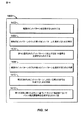
[0085] 図13は、ニアフィールド通信のために信号を整形するためのプロセスを示すフローチャートである。ブロック1302は、複数のビットパターンを記憶するステップを示す。ブロック1304は、複数のビットパターンから第1のビットパターンを選択することを示し、第1のビットパターンは、第1の選択されたビットパターンに対応するパルスパターンをもつ第1の波形(MP1)を生成するために使用される。ブロック1308は、複数のビットパターンから第2のビットパターンを選択することを示し、第2のビットパターンは、第2の選択されたビットパターンに対応するパルスパターンをもつ第2の波形(MP2)を生成するために使用される。ブロック1312において、プロセス1300は、第1の波形と第2の波形との間の差に基づいてキャリア周波数においてパルス幅変調信号を生成する。
FIG. 13 is a flowchart illustrating a process for shaping a signal for near-field communication.
[0086] いくつかの実装形態では、1つまたは複数のメモリユニットが複数のビットパターンを記憶する。第1の回路が複数のビットパターンのうちの第1のビットパターンを選択する。第1の回路は、第1の選択されたビットパターンに対応するパルスパターンをもつ第1の波形(MP1)を生成する。第1の回路は複数のビットパターンのうちの第2のビットパターンを選択する。第1の回路は、第2の選択されたビットパターンに対応するパルスパターンをもつ第2の波形(MP2)を生成する。増幅器が、第1の波形と第2の波形とに基づいてキャリア周波数においてパルス幅変調信号を生成する。 [0086] In some implementations, one or more memory units store multiple bit patterns. The first circuit selects a first bit pattern among the plurality of bit patterns. The first circuit generates a first waveform (MP1) having a pulse pattern corresponding to the first selected bit pattern. The first circuit selects a second bit pattern among the plurality of bit patterns. The first circuit generates a second waveform (MP2) having a pulse pattern corresponding to the second selected bit pattern. An amplifier generates a pulse width modulated signal at the carrier frequency based on the first waveform and the second waveform.
[0087] いくつかの実装形態では、さらなるステップは、パルス幅変調信号の第2の回路より高次の高調波をフィルタすることと、ニアフィールド通信(NFC)送信信号を生成することとを備える。いくつかの実装形態では、第2の回路が、より高次の高調波をフィルタし、ニアフィールド通信(NFC)送信信号を生成する。送信機が、ニアフィールド通信(NFC)送信信号を送信する。ビットパターンは、各プロトコル、変調インデックス、およびデータレート組合せについてより高次の高調波を低減するためにパルス幅変調信号を整形する。 [0087] In some implementations, further steps comprise filtering higher order harmonics than the second circuit of the pulse width modulated signal and generating a near field communication (NFC) transmission signal. . In some implementations, the second circuit filters higher order harmonics and generates a near field communication (NFC) transmission signal. A transmitter transmits a near field communication (NFC) transmission signal. The bit pattern shapes the pulse width modulated signal to reduce higher order harmonics for each protocol, modulation index, and data rate combination.
[0088] オーバーシュートおよびアンダーシュートを低減するために、いくつかの実装形態は位相ステップのN要素シーケンスを定義し、ここにおいて、Nは2を超える。第1の要素が第1の位相に対応する。第Nの要素が第2の位相に対応する。第2〜N−1の要素が、第1の位相から第2の位相への遷移における異なる位相ステップに対応する。第2〜N−1の要素は、第2の位相が第1の位相を超えるときに単調に増加する。第2〜N−1の要素は、第2の位相が第1の位相よりも小さいときに単調に減少する。いくつかの実装形態は、位相ステップのN要素シーケンスの各々のために整形された信号を生成し、ここにおいて、各位相ステップのために選択された第1のビットパターンと各位相ステップのための第2のビットパターンとが位相ステップに対応し、それにより、第1の位相から第2の位相への遷移におけるアンダーシュートとオーバーシュートの両方が低減する。Nは、オーバーシュートおよびアンダーシュートを低減するために遷移時間に応じて、3と32との間で変動し得る。 [0088] To reduce overshoot and undershoot, some implementations define an N-element sequence of phase steps, where N is greater than two. The first element corresponds to the first phase. The Nth element corresponds to the second phase. The second through N-1 elements correspond to different phase steps in the transition from the first phase to the second phase. The second to (N-1) th elements increase monotonously when the second phase exceeds the first phase. The 2nd to (N-1) th elements monotonously decrease when the second phase is smaller than the first phase. Some implementations generate a shaped signal for each of the N-element sequences of phase steps, where the first bit pattern selected for each phase step and for each phase step The second bit pattern corresponds to a phase step, thereby reducing both undershoot and overshoot in the transition from the first phase to the second phase. N can vary between 3 and 32 depending on the transition time to reduce overshoot and undershoot.
[0089] 図14に、ニアフィールド通信のために信号を整形するために使用されるデバイスの要素を示す。デバイス1400は、複数のビットパターンを記憶するための手段1402を備える。デバイス1400は、複数のビットパターンから第1のビットパターンを選択するための手段1404と、第1の選択されたビットパターンに対応するパルスパターンをもつ第1の信号を生成するための手段1406とをさらに備える。デバイス1400は、複数のビットパターンから第2のビットパターンを選択するための手段1408と、第2の選択されたビットパターンに対応するパルスパターンをもつ第2の信号を生成するための手段1410とをさらに備える。デバイス1400は、第1の波形と第2の波形とに基づいてキャリア周波数においてパルス幅変調信号を生成するための手段1412をさらに備える。たとえば、パルス幅変調信号生成手段1412は、差動出力を形成するために一方の波形を他方の波形から減算し得る。
[0089] FIG. 14 shows the elements of a device used to shape a signal for near-field communication.
[0090] 複数のビットパターン記憶手段1402は、図13に示されたブロック1302に関して上記で説明した機能のうちの1つまたは複数を実行するように構成され得る。記憶手段1402は、図3に示された、プロセッサ312とメモリ314とのうちの1つまたは複数を含み得る。第1のビットパターンを選択するための手段1404は、ブロック1304に関して上記で説明した機能のうちの1つまたは複数を実行するように構成され得る。選択手段1404は、図3に示された、プロセッサ312とメモリ314とのうちの1つまたは複数を含み得る。第1の信号を生成する手段1406は、ブロック1312に関して上記で説明した機能のうちの1つまたは複数を実行するように構成され得る。第1の信号を生成する手段1406は、プロセッサ312とメモリ314とのうちの1つまたは複数を含み得る。
[0090] The plurality of bit pattern storage means 1402 may be configured to perform one or more of the functions described above with respect to the
[0091] 第2のビットパターンを選択する手段1408は、ブロック1308に関して上記で説明した機能のうちの1つまたは複数を実行するように構成され得る。第2のビットパターンを選択する手段1408は、図3に示された、プロセッサ312とメモリ314とのうちの1つまたは複数を含み得る。第2の信号を生成する手段1410は、ブロック1312に関して上記で説明した機能のうちの1つまたは複数を実行するように構成され得る。第2の信号を生成する手段1410は、プロセッサ312とメモリ314とのうちの1つまたは複数を含み得る。ためのパルス幅変調信号を生成する手段1412は、ブロック1312に関して上記で説明した機能のうちの1つまたは複数を実行するように構成され得る。パルス幅変調信号を生成する手段1412は、プロセッサ312と、メモリ314と、RFアナログブロック316と、LO生成器318と、増幅器320とのうちの1つまたは複数を含み得る。
[0091] The
[0092] いくつかの実装形態では、1つまたは複数のメモリユニットが複数のビットパターンを記憶する。第1の回路が複数のビットパターンのうちの第1のビットパターンを選択する。第1の回路は、第1の選択されたビットパターンに対応するパルスパターンをもつ第1の波形(MP1)を生成する。第1の回路は複数のビットパターンのうちの第2のビットパターンを選択する。第1の回路は、第2の選択されたビットパターンに対応するパルスパターンをもつ第2の波形(MP2)を生成する。増幅器は、第1の波形と第2の波形との間の差に基づいてキャリア周波数においてパルス幅変調信号を生成する。 [0092] In some implementations, one or more memory units store multiple bit patterns. The first circuit selects a first bit pattern among the plurality of bit patterns. The first circuit generates a first waveform (MP1) having a pulse pattern corresponding to the first selected bit pattern. The first circuit selects a second bit pattern among the plurality of bit patterns. The first circuit generates a second waveform (MP2) having a pulse pattern corresponding to the second selected bit pattern. The amplifier generates a pulse width modulated signal at the carrier frequency based on the difference between the first waveform and the second waveform.
[0093] いくつかの実装形態では、本デバイスは、パルス幅変調信号の第2の回路より高次の高調波をフィルタするための手段と、ニアフィールド通信(NFC)送信信号を生成するための手段とをさらに備える。いくつかの実装形態では、第2の回路が、より高次の高調波をフィルタし、ニアフィールド通信(NFC)送信信号を生成する。送信機が、ニアフィールド通信(NFC)送信信号を送信するための手段を与える。ビットパターンは、各プロトコル、変調インデックス、およびデータレート組合せについてより高次の高調波を低減するためにパルス幅変調信号を整形する。 [0093] In some implementations, the device includes means for filtering higher order harmonics than the second circuit of the pulse width modulated signal, and for generating a near field communication (NFC) transmission signal. Means. In some implementations, the second circuit filters higher order harmonics and generates a near field communication (NFC) transmission signal. A transmitter provides a means for transmitting a near field communication (NFC) transmission signal. The bit pattern shapes the pulse width modulated signal to reduce higher order harmonics for each protocol, modulation index, and data rate combination.
[0094] オーバーシュートおよびアンダーシュートを低減するために、いくつかの実装形態は、位相ステップのN要素シーケンスを定義するための手段を含んでおり、ここにおいて、Nは2を超える。第1の要素が第1の位相に対応する。第Nの要素が第2の位相に対応する。第2〜N−1の要素が、第1の位相から第2の位相への遷移における異なる位相ステップに対応する。第2〜N−1の要素は、第2の位相が第1の位相を超えるときに単調に増加する。第2〜N−1の要素は、第2の位相が第1の位相よりも小さいときに単調に減少する。いくつかの実装形態は、位相ステップのN要素シーケンスの各々のために整形された信号を生成し、ここにおいて、各位相ステップのために選択された第1のビットパターンと各位相ステップのための第2のビットパターンとが位相ステップに対応し、それにより、第1の位相から第2の位相への遷移におけるアンダーシュートとオーバーシュートの両方が低減する。Nは、オーバーシュートおよびアンダーシュートを低減するために遷移時間に応じて、3と32との間で変動し得る。 [0094] In order to reduce overshoot and undershoot, some implementations include means for defining an N-element sequence of phase steps, where N is greater than two. The first element corresponds to the first phase. The Nth element corresponds to the second phase. The second through N-1 elements correspond to different phase steps in the transition from the first phase to the second phase. The second to (N-1) th elements increase monotonously when the second phase exceeds the first phase. The 2nd to (N-1) th elements monotonously decrease when the second phase is smaller than the first phase. Some implementations generate a shaped signal for each of the N-element sequences of phase steps, where the first bit pattern selected for each phase step and for each phase step The second bit pattern corresponds to a phase step, thereby reducing both undershoot and overshoot in the transition from the first phase to the second phase. N can vary between 3 and 32 depending on the transition time to reduce overshoot and undershoot.
[0095] 本明細書で開示する実装形態に関して説明した様々な例示的な論理ブロック、モジュール、回路、およびアルゴリズムステップは、電子ハードウェア、コンピュータソフトウェア、または両方の組合せとして実装され得る。ハードウェアとソフトウェアのこの互換性を明確に示すために、様々な例示的な構成要素、ブロック、モジュール、回路、およびステップを、上記では概してそれらの機能に関して説明した。そのような機能をハードウェアとして実装するか、ソフトウェアとして実装するかは、特定の適用例および全体的なシステムに課される設計制約に依存する。説明した機能は、特定の適用例ごとに様々な方法で実装され得るが、そのような実装の決定は、本出願の実装の範囲からの逸脱を生じるものと解釈すべきではない。 [0095] The various exemplary logic blocks, modules, circuits, and algorithm steps described with respect to the implementations disclosed herein may be implemented as electronic hardware, computer software, or a combination of both. To clearly illustrate this interchangeability of hardware and software, various illustrative components, blocks, modules, circuits, and steps have been described above generally in terms of their functionality. Whether such functionality is implemented as hardware or software depends upon the particular application and design constraints imposed on the overall system. Although the described functionality can be implemented in a variety of ways for a particular application, such implementation decisions should not be construed as causing a departure from the scope of implementation of the present application.
[0096] 本明細書で開示した実装形態に関して説明した様々な例示的なブロック、モジュール、および回路は、汎用プロセッサ、デジタル信号プロセッサ(DSP)、特定用途向け集積回路(ASIC)、フィールドプログラマブルゲートアレイ(FPGA)または他のプログラマブル論理デバイス、個別ゲートまたはトランジスタ論理、個別ハードウェア構成要素、あるいは本明細書で説明した機能を実行するように設計されたそれらの任意の組合せを用いて実装または実行され得る。汎用プロセッサはマイクロプロセッサであり得るが、代替として、プロセッサは、任意の従来のプロセッサ、コントローラ、マイクロコントローラ、または状態機械であり得る。プロセッサはまた、コンピューティングデバイスの組合せ、たとえば、DSPとマイクロプロセッサとの組合せ、複数のマイクロプロセッサ、DSPコアと連携する1つまたは複数のマイクロプロセッサ、あるいは任意の他のそのような構成として実装され得る。 [0096] Various exemplary blocks, modules, and circuits described with respect to the implementations disclosed herein are general purpose processors, digital signal processors (DSPs), application specific integrated circuits (ASICs), field programmable gate arrays. (FPGA) or other programmable logic device, individual gate or transistor logic, individual hardware components, or any combination thereof designed to perform the functions described herein. obtain. A general purpose processor may be a microprocessor, but in the alternative, the processor may be any conventional processor, controller, microcontroller, or state machine. The processor is also implemented as a combination of computing devices, eg, a combination of a DSP and a microprocessor, a plurality of microprocessors, one or more microprocessors associated with a DSP core, or any other such configuration. obtain.
[0097] 本明細書で開示した実装委形態に関して説明した方法またはアルゴリズムのステップおよび機能は、直接ハードウェアで実施されるか、プロセッサによって実行されるソフトウェアモジュールで実施されるか、またはその2つの組合せで実施され得る。ソフトウェアで実装される場合、機能は、1つまたは複数の命令またはコードとして有形の非一時的コンピュータ可読媒体上に記憶されるか、あるいは有形の非一時的コンピュータ可読媒体を介して送信され得る。ソフトウェアモジュールは、ランダムアクセスメモリ(RAM)、フラッシュメモリ、読取り専用メモリ(ROM)、電気的プログラマブルROM(EPROM)、電気的消去可能プログラマブルROM(EEPROM(登録商標))、レジスタ、ハードディスク、リムーバブルディスク、CD ROM、または当技術分野で知られている任意の他の形態の記憶媒体中に常駐し得る。記憶媒体は、プロセッサがその記憶媒体から情報を読み取り、その記憶媒体に情報を書き込み得るように、プロセッサに結合される。代替として、記憶媒体はプロセッサに一体化され得る。本明細書で使用するディスク(disk)およびディスク(disc)は、コンパクトディスク(disc)(CD)、レーザーディスク(登録商標)(disc)、光ディスク(disc)、デジタル多用途ディスク(disc)(DVD)、フロッピー(登録商標)ディスク(disk)およびBlu−ray(登録商標)ディスク(disc)を含み、ディスク(disk)は、通常、データを磁気的に再生し、ディスク(disc)は、データをレーザで光学的に再生する。上記の組合せもコンピュータ可読媒体の範囲内に含まれるべきである。プロセッサおよび記憶媒体はASIC中に常駐し得る。ASICはユーザ端末内に常駐し得る。代替として、プロセッサおよび記憶媒体は、ユーザ端末中に個別構成要素として常駐し得る。 [0097] The method or algorithm steps and functions described with respect to implementations disclosed herein may be implemented directly in hardware, in software modules executed by a processor, or two of them. It can be implemented in combination. If implemented in software, the functions may be stored as one or more instructions or code on a tangible non-transitory computer readable medium or transmitted via a tangible non-transitory computer readable medium. Software modules include random access memory (RAM), flash memory, read only memory (ROM), electrically programmable ROM (EPROM), electrically erasable programmable ROM (EEPROM (registered trademark)), registers, hard disk, removable disk, It may reside in a CD ROM, or any other form of storage medium known in the art. A storage medium is coupled to the processor such that the processor can read information from, and write information to, the storage medium. In the alternative, the storage medium may be integral to the processor. As used herein, a disk and a disc are a compact disc (CD), a laser disc (registered trademark) (disc), an optical disc (disc), a digital versatile disc (DVD). ), Floppy disk, and Blu-ray disk, which normally reproduces data magnetically, and the disk stores data. Reproduce optically with a laser. Combinations of the above should also be included within the scope of computer-readable media. The processor and the storage medium can reside in an ASIC. The ASIC may reside in the user terminal. In the alternative, the processor and the storage medium may reside as discrete components in a user terminal.
[0098] 本開示を要約するために、本出願のいくつかの態様、利点および新規の特徴について、本明細書で説明してきた。本出願の特定の実装形態に従って、必ずしもすべてのそのような利点が達成されるとは限らないことを理解されたい。したがって、本出願は、必ずしも、本明細書で教示されるか、または示唆され得る他の利点を達成する必要なしに、本明細書で教示する1つの利点または利点のグループを達成するか、または最適化する形で実施されるか、または行われ得る。 [0098] In order to summarize the present disclosure, several aspects, advantages and novel features of the present application have been described herein. It should be understood that not all such advantages may be achieved in accordance with certain implementations of the present application. Accordingly, this application does not necessarily achieve one advantage or group of advantages taught herein without having to achieve the other advantages taught or suggested herein, or It can be implemented or performed in an optimized manner.
[0099] 上記で説明した実装形態の様々な修正は当業者には容易に明らかであり得、本明細書で定義した一般原理は、本出願の趣旨または範囲から逸脱することなく他の実装形態に適用され得る。したがって、本出願は、本明細書で示した実装形態に限定されるものではなく、本明細書で開示した原理および新規の特徴に一致する最も広い範囲を与えられるべきである。
以下に、出願当初の特許請求の範囲に記載された発明を付記する。
[C1]
複数のビットパターンを記憶するように構成されたメモリユニットと、
前記複数のビットパターンのうちの第1の選択された1つを使用して第1の信号を生成するように構成され、前記複数のビットパターンのうちの第2の選択された1つに対応する第2の信号を生成するように構成された第1の回路と、
前記第1の回路に結合され、前記第1の信号と前記第2の信号とに基づいてキャリア周波数においてパルス幅変調信号を生成するように構成された増幅器とを備えるワイヤレス通信のための装置。
[C2]
ニアフィールド通信(NFC)送信信号を生成するために前記パルス幅変調信号のより高次の高調波をフィルタするように構成された第2の回路をさらに備える、C1に記載の装置。
[C3]
前記複数のビットパターンは、各プロトコル、変調インデックス、およびデータレート組合せについてより高次の高調波を低減するために前記パルス幅変調信号を整形するビットパターンを備える、C1に記載の装置。
[C4]
前記第2の回路に動作可能に結合された送信機をさらに備え、前記送信機が、前記ニアフィールド通信(NFC)送信信号を送信するように構成された、C2に記載の装置。
[C5]
前記増幅器がD級電力増幅器である、C1に記載の装置。
[C6]
前記第2の回路が整合ネットワークフィルタである、C2に記載の装置。
[C7]
前記複数のビットパターンの各々が32ビットを含んでいる、C3に記載の装置。
[C8]
前記複数のビットパターンのうちの前記第1の選択された1つは、送信コード化ビットが0であるか1であるかに基づいて選択され、前記複数のビットパターンのうちの前記第2の選択された1つは、送信コード化ビットが0であるか1であるかに基づいて選択される、C1に記載の装置。
[C9]
前記第1の回路が、前記キャリア周波数の各サイクルについて前記複数のビットパターンのうちの1つを選択するようにさらに構成された、C1に記載の装置。
[C10]
前記複数のビットパターンが、50%未満のデューティサイクルをもつ少なくとも1つのビットパターンを含む、複数の異なるデューティサイクルをもつビットパターンを含む、C1に記載の装置。
[C11]
前記複数のビットパターンが、第1の位相から第2の位相への遷移における異なる位相ステップに対応するビットパターンを含む、C1に記載の装置。
[C12]
前記第1の回路は、位相遷移におけるアンダーシュートとオーバーシュートの両方を低減するために、最初に、前記第1の位相に対応する前記複数のビットパターンのうちの1つを選択し、次いで、前記第1の位相から前記第2の位相への前記遷移における異なる位相ステップに対応する前記複数のビットパターンのうちの1つを選択し、最後に、前記第2の位相に対応する前記複数のビットパターンのうちの1つを選択するように構成された、C11に記載の装置。
[C13]
前記ニアフィールド通信(NFC)送信信号が、128に分周されたキャリア周波数のデータレートおよび90%〜100%の変調インデックス、64に分周されたキャリア周波数のデータレートおよび25%〜100%の変調インデックス、32に分周されたキャリア周波数のデータレートおよび25%〜100%の変調インデックス、または16に分周されたキャリア周波数のデータレートおよび25%〜100%の変調インデックスのうちの1つから選択された特性を有する、タイプAプロキシミティニアフィールド通信(NFC)信号になるように構成された、C1に記載の装置。
[C14]
前記ニアフィールド通信(NFC)送信信号が、8%〜15%の変調インデックスと、128に分周されたキャリア周波数、64に分周されたキャリア周波数、32に分周されたキャリア周波数、または16に分周されたキャリア周波数のうちの1つから選択されたデータレートとを有する、タイプBプロキシミティニアフィールド通信信号になるように構成された、C1に記載の装置。
[C15]
前記ニアフィールド通信(NFC)送信信号、64に分周されたキャリア周波数のデータレートおよび8%〜14%の変調インデックス、または32に分周されたキャリア周波数のデータレートおよび8%〜14%の変調インデックスのうちの1つから選択された特性を有する、タイプFプロキシミティニアフィールド通信信号になるように構成された、C1に記載の装置。
[C16]
前記ニアフィールド通信(NFC)送信信号が、512に分周されたキャリア周波数のデータレートおよび10%〜100%の変調インデックス、ならびに8192に分周されたキャリア周波数および10%〜100%の変調インデックスのうちの1つから選択された特性をもつ、ビシニティニアフィールド通信信号になるように構成された、C1に記載の装置。
[C17]
ニアフィールド通信(NFC)のために信号を整形するための方法であって、
複数のビットパターンを記憶することと、
前記複数のビットパターンのうちの第1のビットパターンを選択することと、
前記複数のビットパターンのうちの第2のビットパターンを選択することと、
前記第1のビットパターンと前記第2のビットパターンとの間の差に基づいてキャリア周波数においてパルス幅変調信号を生成することとを備える、整形された信号を生成することを備える、方法。
[C18]
前記第1の選択されたビットパターンに対応する第1の信号を生成することと、前記第2の選択されたビットパターンに対応する第2の信号を生成することとをさらに備え、ここにおいて、パルス幅変調信号を生成することが、前記第1の信号と前記第2の信号とを増幅器に入力することを備え、ここにおいて、前記パルス幅変調信号が前記増幅器からの出力信号である、C17に記載の方法。
[C19]
前記パルス幅変調信号のより高次の高調波をフィルタすることと、
ニアフィールド通信(NFC)送信信号を生成することとをさらに備える、C17に記載の方法。
[C20]
各プロトコル、変調インデックス、およびデータレート組合せについて、より高次の高調波を低減するために前記パルス幅変調信号を整形する前記複数のビットパターンから選択することをさらに備える、C17に記載の方法。
[C21]
前記ニアフィールド通信(NFC)送信信号を送信することをさらに備える、C19に記載の方法。
[C22]
位相ステップのN要素シーケンスを定義することと、ここにおいて、Nが2を超え、ここにおいて、第1の要素が第1の位相に対応し、第N番目の要素が第2の位相に対応し、第2〜N−1の要素が、前記第1の位相から前記第2の位相への遷移における異なる位相ステップに対応し、前記第2〜N−1の要素は、前記第2の位相が前記第1の位相を超えるときに単調に増加し、前記第2〜N−1の要素は、前記第2の位相が前記第1の位相よりも小さいときに単調に減少する、
位相ステップの前記N要素シーケンスの各々について整形された信号を生成することと、ここにおいて、各位相ステップについて選択された前記第1のビットパターンと各位相ステップについて前記第2のビットパターンとが前記位相ステップに対応し、それにより、前記第1の位相から前記第2の位相への前記遷移におけるアンダーシュートとオーバーシュートの両方が低減するをさらに備える、C17に記載の方法。
[C23]
位相ステップの前記N要素シーケンスが、3≦N≦32となるような、整数個の位相ステップを含んでいる、C22に記載の方法。
[C24]
ニアフィールド通信(NFC)のために信号を整形するためのデバイスであって、
複数のビットパターンを記憶するための手段と、
前記複数のビットパターンのうちの第1のビットパターンを選択するための手段と、
前記第1の選択されたビットパターンに対応する第1の信号を生成するための手段と、
前記複数のビットパターンのうちの第2のビットパターンを選択するための手段と、
前記第2の選択されたビットパターンに対応する第2を生成するための手段と、
第1の波形と第2の波形とに基づいてキャリア周波数においてパルス幅変調信号を生成するための手段とを備える、信号生成器を備える、デバイス。
[C25]
複数のビットパターンを記憶するための前記手段がメモリユニットを備え、第1のビットパターンを選択するための前記手段が第1の回路を備え、第1の信号を生成するための前記手段が前記第1の回路を備え、第2のビットパターンを選択するための前記手段が第1の回路を備え、第2の信号を生成するための前記手段が前記第1の回路を備え、パルス幅変調信号を生成するための前記手段が増幅器を備える、C24に記載のデバイス。
[C26]
前記パルス幅変調信号のより高次の高調波をフィルタするための手段と、
前記フィルタされたパルス幅変調信号からニアフィールド通信送信信号を生成するための手段とをさらに備える、C24に記載のデバイス。
[C27]
より高次の高調波をフィルタするための前記手段が第2の回路を備え、ニアフィールド通信送信信号を生成するための前記手段が前記第2の回路を備える、C26に記載のデバイス。
[C28]
実行されたとき、
メモリユニットによって複数のビットパターンを記憶することと、
第1の回路によって前記複数のビットパターンのうちの第1のビットパターンを選択することと、
第1の回路によって前記第1の選択されたビットパターンに対応する第1の信号を生成することと、
第1の回路によって前記複数のビットパターンのうちの第2のビットパターンを選択することと、
第1の回路によって前記第2の選択されたビットパターンに対応する第2の信号を生成することと、
増幅器によって前記第1の信号と前記第2の信号とに基づいてキャリア周波数においてパルス幅変調信号を生成することとを装置に行わせることによって、整形された信号を生成することを前記装置に行わせる命令を備える非一時的コンピュータ可読媒体。
[C29]
実行されたとき、
第2の回路によって前記パルス幅変調信号のより高次の高調波をフィルタすることと、
前記第2の回路によってニアフィールド通信(NFC)送信信号を生成することとを装置に行わせる命令をさらに備える、C28に記載の非一時的コンピュータ可読媒体。
[C30]
複数のビットパターンを記憶するように構成されたメモリユニットと、
前記複数のビットパターンのうちの第1の選択された1つに対応する第1の信号を生成するように構成され、前記複数のビットパターンのうちの第2の選択された1つに対応する第2の信号を生成するように構成された回路と、
前記回路に結合され、前記第1の信号と前記第2の信号とに基づいてキャリア周波数においてパルス幅変調信号を生成するように構成された増幅器とを備える、ワイヤレス通信のためのプロセッサ。
[0099] Various modifications to the implementations described above will be readily apparent to those skilled in the art, and the generic principles defined herein may be used in other implementations without departing from the spirit or scope of the application. Can be applied to. Accordingly, this application is not intended to be limited to the implementations shown herein but is to be accorded the widest scope consistent with the principles and novel features disclosed herein.
The invention described in the scope of claims at the beginning of the application will be appended.
[C1]
A memory unit configured to store a plurality of bit patterns;
Configured to generate a first signal using a first selected one of the plurality of bit patterns and corresponding to a second selected one of the plurality of bit patterns A first circuit configured to generate a second signal to:
An apparatus for wireless communication comprising an amplifier coupled to the first circuit and configured to generate a pulse width modulated signal at a carrier frequency based on the first signal and the second signal.
[C2]
The apparatus of C1, further comprising a second circuit configured to filter higher order harmonics of the pulse width modulated signal to generate a near field communication (NFC) transmission signal.
[C3]
The apparatus of C1, wherein the plurality of bit patterns comprises a bit pattern that shapes the pulse width modulated signal to reduce higher order harmonics for each protocol, modulation index, and data rate combination.
[C4]
The apparatus of C2, further comprising a transmitter operably coupled to the second circuit, wherein the transmitter is configured to transmit the near-field communication (NFC) transmission signal.
[C5]
The apparatus according to C1, wherein the amplifier is a class D power amplifier.
[C6]
The apparatus of C2, wherein the second circuit is a matched network filter.
[C7]
The apparatus of C3, wherein each of the plurality of bit patterns includes 32 bits.
[C8]
The first selected one of the plurality of bit patterns is selected based on whether a transmission coded bit is 0 or 1, and the second one of the plurality of bit patterns is selected. The apparatus of C1, wherein the selected one is selected based on whether the transmission coded bits are 0 or 1.
[C9]
The apparatus of C1, wherein the first circuit is further configured to select one of the plurality of bit patterns for each cycle of the carrier frequency.
[C10]
The apparatus of C1, wherein the plurality of bit patterns includes bit patterns having a plurality of different duty cycles, including at least one bit pattern having a duty cycle of less than 50%.
[C11]
The apparatus of C1, wherein the plurality of bit patterns includes bit patterns corresponding to different phase steps in a transition from a first phase to a second phase.
[C12]
The first circuit first selects one of the plurality of bit patterns corresponding to the first phase to reduce both undershoot and overshoot in phase transitions, and then Selecting one of the plurality of bit patterns corresponding to different phase steps in the transition from the first phase to the second phase, and finally, the plurality of bit patterns corresponding to the second phase The apparatus of C11, configured to select one of the bit patterns.
[C13]
The near-field communication (NFC) transmission signal has a carrier frequency data rate divided by 128 and a modulation index of 90% to 100%, a carrier frequency data rate divided by 64 and 25% to 100%. One of the modulation index, the data rate of the carrier frequency divided by 32 and the modulation index of 25% to 100%, or the data rate of the carrier frequency divided by 16 and the modulation index of 25% to 100% The apparatus of C1, wherein the apparatus is configured to be a Type A Proximity Near Field Communication (NFC) signal having characteristics selected from:
[C14]
The near field communication (NFC) transmission signal has a modulation index of 8% to 15%, a carrier frequency divided by 128, a carrier frequency divided by 64, a carrier frequency divided by 32, or 16 The apparatus of C1, wherein the apparatus is configured to be a type B proximity field communication signal having a data rate selected from one of the carrier frequencies divided into two.
[C15]
Near field communication (NFC) transmission signal, carrier frequency data rate divided by 64 and modulation index of 8% to 14%, or carrier frequency data rate divided by 32 and 8% to 14% The apparatus of C1, configured to be a Type F Proximity Near Field communication signal with characteristics selected from one of the modulation indices.
[C16]
The near-field communication (NFC) transmission signal has a carrier frequency data rate divided by 512 and a modulation index of 10% to 100%, and a carrier frequency divided by 8192 and a modulation index of 10% to 100%. The apparatus of C1, wherein the apparatus is configured to be a vicininia field communication signal having a characteristic selected from one of the following:
[C17]
A method for shaping a signal for near field communication (NFC) comprising:
Storing a plurality of bit patterns;
Selecting a first bit pattern of the plurality of bit patterns;
Selecting a second bit pattern of the plurality of bit patterns;
Generating a shaped signal comprising generating a pulse width modulated signal at a carrier frequency based on a difference between the first bit pattern and the second bit pattern.
[C18]
Generating a first signal corresponding to the first selected bit pattern; and generating a second signal corresponding to the second selected bit pattern, wherein Generating a pulse width modulated signal comprises inputting the first signal and the second signal to an amplifier, wherein the pulse width modulated signal is an output signal from the amplifier, C17 The method described in 1.
[C19]
Filtering higher order harmonics of the pulse width modulated signal;
Generating the near field communication (NFC) transmission signal.
[C20]
The method of C17, further comprising, for each protocol, modulation index, and data rate combination, selecting from the plurality of bit patterns that shape the pulse width modulated signal to reduce higher order harmonics.
[C21]
The method of C19, further comprising transmitting the near field communication (NFC) transmission signal.
[C22]
Defining an N element sequence of phase steps, where N is greater than 2, where the first element corresponds to the first phase and the Nth element corresponds to the second phase. , The second to N−1 elements correspond to different phase steps in the transition from the first phase to the second phase, and the second to N−1 elements have the second phase Monotonically increasing when exceeding the first phase, the second to N-1 elements monotonically decreasing when the second phase is smaller than the first phase;
Generating a shaped signal for each of the N element sequences of phase steps, wherein the first bit pattern selected for each phase step and the second bit pattern for each phase step are The method of C17, further comprising: corresponding to a phase step, thereby reducing both undershoot and overshoot in the transition from the first phase to the second phase.
[C23]
The method of C22, wherein the N element sequence of phase steps includes an integer number of phase steps such that 3 ≦ N ≦ 32.
[C24]
A device for shaping a signal for near field communication (NFC),
Means for storing a plurality of bit patterns;
Means for selecting a first bit pattern of the plurality of bit patterns;
Means for generating a first signal corresponding to the first selected bit pattern;
Means for selecting a second bit pattern of the plurality of bit patterns;
Means for generating a second corresponding to the second selected bit pattern;
A device comprising a signal generator comprising means for generating a pulse width modulated signal at a carrier frequency based on a first waveform and a second waveform.
[C25]
The means for storing a plurality of bit patterns comprises a memory unit, the means for selecting a first bit pattern comprises a first circuit, and the means for generating a first signal comprises the means A first circuit, the means for selecting a second bit pattern comprises a first circuit, the means for generating a second signal comprises the first circuit, and pulse width modulation; The device of C24, wherein the means for generating a signal comprises an amplifier.
[C26]
Means for filtering higher harmonics of the pulse width modulated signal;
The device of C24, further comprising means for generating a near-field communication transmission signal from the filtered pulse width modulated signal.
[C27]
The device of C26, wherein the means for filtering higher harmonics comprises a second circuit, and the means for generating a near-field communication transmission signal comprises the second circuit.
[C28]
When executed
Storing a plurality of bit patterns by a memory unit;
Selecting a first bit pattern of the plurality of bit patterns by a first circuit;
Generating a first signal corresponding to the first selected bit pattern by a first circuit;
Selecting a second bit pattern of the plurality of bit patterns by a first circuit;
Generating a second signal corresponding to the second selected bit pattern by a first circuit;
Producing a shaped signal by causing the apparatus to generate a pulse width modulated signal at a carrier frequency based on the first signal and the second signal by an amplifier. A non-transitory computer readable medium comprising instructions to be executed.
[C29]
When executed
Filtering higher order harmonics of the pulse width modulated signal by a second circuit;
The non-transitory computer-readable medium according to C28, further comprising instructions that cause the apparatus to generate a near-field communication (NFC) transmission signal by the second circuit.
[C30]
A memory unit configured to store a plurality of bit patterns;
Configured to generate a first signal corresponding to a first selected one of the plurality of bit patterns and corresponding to a second selected one of the plurality of bit patterns A circuit configured to generate a second signal;
A processor for wireless communication comprising an amplifier coupled to the circuit and configured to generate a pulse width modulated signal at a carrier frequency based on the first signal and the second signal.
Claims (30)
前記複数のビットパターンのうちの第1の選択された1つを使用して第1の信号を生成するように構成され、前記複数のビットパターンのうちの第2の選択された1つに対応する第2の信号を生成するように構成された第1の回路と、
前記第1の回路に結合され、前記第1の信号と前記第2の信号との間の差に基づいてキャリア周波数においてパルス幅変調信号を生成するように構成された増幅器と
を備えるワイヤレス通信のための装置。 A memory unit configured to store a plurality of bit patterns;
Configured to generate a first signal using a first selected one of the plurality of bit patterns and corresponding to a second selected one of the plurality of bit patterns A first circuit configured to generate a second signal to:
Wireless communication comprising: an amplifier coupled to the first circuit and configured to generate a pulse width modulated signal at a carrier frequency based on a difference between the first signal and the second signal Equipment for.
整形信号を生成すること、を備え、前記整形信号を生成することは、
複数のビットパターンを記憶することと、
前記複数のビットパターンのうちの第1のビットパターンを選択することと、
前記複数のビットパターンのうちの第2のビットパターンを選択することと、
前記第1のビットパターンと前記第2のビットパターンとの間の差に基づいてキャリア周波数においてパルス幅変調信号を生成することと
を備える、方法。 A method for shaping a signal for near field communication (NFC) comprising:
Generating a shaped signal, and generating the shaped signal,
Storing a plurality of bit patterns;
Selecting a first bit pattern of the plurality of bit patterns;
Selecting a second bit pattern of the plurality of bit patterns;
Generating a pulse width modulated signal at a carrier frequency based on a difference between the first bit pattern and the second bit pattern.
選択された前記第2のビットパターンに対応する第2の信号を生成することと
をさらに備え、
ここにおいて、パルス幅変調信号を生成することが、前記第1の信号と前記第2の信号とを増幅器に入力することを備え、ここにおいて、前記パルス幅変調信号が前記増幅器からの出力信号である、請求項17に記載の方法。 Generating a first signal corresponding to the selected first bit pattern;
Generating a second signal corresponding to the selected second bit pattern;
Here, generating a pulse width modulated signal comprises inputting the first signal and the second signal to an amplifier, wherein the pulse width modulated signal is an output signal from the amplifier. The method of claim 17, wherein:
ニアフィールド通信(NFC)送信信号を生成することと
をさらに備える、請求項17に記載の方法。 Filtering higher order harmonics of the pulse width modulated signal;
The method of claim 17, further comprising generating a near field communication (NFC) transmission signal.
位相ステップの前記N要素シーケンスの各々について整形された信号を生成することと、ここにおいて、各位相ステップについて選択された前記第1のビットパターンと各位相ステップについて前記第2のビットパターンとが前記位相ステップに対応し、それにより、前記第1の位相から前記第2の位相への前記遷移におけるアンダーシュートとオーバーシュートの両方が低減する
をさらに備える、請求項17に記載の方法。 Defining an N element sequence of phase steps, where N is greater than 2, where the first element corresponds to the first phase and the Nth element corresponds to the second phase. , The second to N−1 elements correspond to different phase steps in the transition from the first phase to the second phase, and the second to N−1 elements have the second phase Monotonically increasing when exceeding the first phase, the second to N-1 elements monotonically decreasing when the second phase is smaller than the first phase;
Generating a shaped signal for each of the N element sequences of phase steps, wherein the first bit pattern selected for each phase step and the second bit pattern for each phase step are The method of claim 17, further comprising: corresponding to a phase step, whereby both undershoot and overshoot in the transition from the first phase to the second phase are reduced.
複数のビットパターンを記憶するための手段と、
前記複数のビットパターンのうちの第1のビットパターンを選択するための手段と、
選択された前記第1のビットパターンに対応する第1の波形を生成するための手段と、
前記複数のビットパターンのうちの第2のビットパターンを選択するための手段と、
選択された前記第2のビットパターンに対応する第2の波形を生成するための手段と、
第1の波形と第2の波形との間の差に基づいてキャリア周波数においてパルス幅変調信号を生成するための手段と
を備える、デバイス。 A device for shaping a signal for near field communication (NFC) comprising a signal generator, the signal generator comprising:
Means for storing a plurality of bit patterns;
Means for selecting a first bit pattern of the plurality of bit patterns;
Means for generating a first waveform corresponding to the selected first bit pattern;
Means for selecting a second bit pattern of the plurality of bit patterns;
Means for generating a second waveform corresponding to the selected second bit pattern;
Means for generating a pulse width modulated signal at a carrier frequency based on the difference between the first waveform and the second waveform.
前記フィルタされたパルス幅変調信号からニアフィールド通信送信信号を生成するための手段と
をさらに備える、請求項24に記載のデバイス。 Means for filtering higher harmonics of the pulse width modulated signal;
25. The device of claim 24, further comprising: means for generating a near field communication transmit signal from the filtered pulse width modulated signal.
メモリユニットによって複数のビットパターンを記憶することと、
第1の回路によって前記複数のビットパターンのうちの第1のビットパターンを選択することと、
第1の回路によって選択された前記第1のビットパターンに対応する第1の信号を生成することと、
第1の回路によって前記複数のビットパターンのうちの第2のビットパターンを選択することと、
第1の回路によって選択された前記第2のビットパターンに対応する第2の信号を生成することと、
増幅器によって前記第1の信号と前記第2の信号との間の差に基づいてキャリア周波数においてパルス幅変調信号を生成することと
を装置に行わせることによって、整形された信号を生成することを前記装置に行わせる命令を備える、コンピュータ可読記憶媒体。 When executed
Storing a plurality of bit patterns by a memory unit;
Selecting a first bit pattern of the plurality of bit patterns by a first circuit;
Generating a first signal corresponding to the first bit pattern selected by a first circuit;
Selecting a second bit pattern of the plurality of bit patterns by a first circuit;
Generating a second signal corresponding to the second bit pattern selected by the first circuit;
Generating a shaped signal by causing an apparatus to generate a pulse width modulated signal at a carrier frequency based on a difference between the first signal and the second signal by an amplifier. A computer readable storage medium comprising instructions to be executed by the apparatus.
第2の回路によって前記パルス幅変調信号のより高次の高調波をフィルタすることと、
前記第2の回路によってニアフィールド通信(NFC)送信信号を生成することと
を装置に行わせる命令をさらに備える、請求項28に記載のコンピュータ可読記憶媒体。 When executed
Filtering higher order harmonics of the pulse width modulated signal by a second circuit;
30. The computer readable storage medium of claim 28, further comprising instructions that cause a device to generate a near field communication (NFC) transmission signal by the second circuit.
前記複数のビットパターンのうちの第1の選択された1つに対応する第1の信号を生成するように構成され、前記複数のビットパターンのうちの第2の選択された1つに対応する第2の信号を生成するように構成された回路と、
前記回路に結合され、前記第1の信号と前記第2の信号との間の差に基づいてキャリア周波数においてパルス幅変調信号を生成するように構成された増幅器と
を備える、ワイヤレス通信のためのプロセッサ。 A memory unit configured to store a plurality of bit patterns;
Configured to generate a first signal corresponding to a first selected one of the plurality of bit patterns and corresponding to a second selected one of the plurality of bit patterns A circuit configured to generate a second signal;
An amplifier coupled to the circuit and configured to generate a pulse width modulated signal at a carrier frequency based on a difference between the first signal and the second signal. Processor.
Applications Claiming Priority (5)
| Application Number | Priority Date | Filing Date | Title |
|---|---|---|---|
| US201261706581P | 2012-09-27 | 2012-09-27 | |
| US61/706,581 | 2012-09-27 | ||
| US13/800,065 US8902965B2 (en) | 2012-09-27 | 2013-03-13 | Pulse shaping for generating NFC initiator transmit waveform |
| US13/800,065 | 2013-03-13 | ||
| PCT/US2013/061351 WO2014052291A1 (en) | 2012-09-27 | 2013-09-24 | Pulse shaping for generating nfc initiator transmit waveform |
Publications (3)
| Publication Number | Publication Date |
|---|---|
| JP2016500216A JP2016500216A (en) | 2016-01-07 |
| JP2016500216A5 JP2016500216A5 (en) | 2016-10-13 |
| JP6388867B2 true JP6388867B2 (en) | 2018-09-12 |
Family
ID=50338833
Family Applications (1)
| Application Number | Title | Priority Date | Filing Date |
|---|---|---|---|
| JP2015534594A Active JP6388867B2 (en) | 2012-09-27 | 2013-09-24 | Pulse shaping to generate NFC initiator transmit waveform |
Country Status (6)
| Country | Link |
|---|---|
| US (1) | US8902965B2 (en) |
| EP (1) | EP2901565A1 (en) |
| JP (1) | JP6388867B2 (en) |
| KR (1) | KR20150063436A (en) |
| CN (1) | CN104662808B (en) |
| WO (1) | WO2014052291A1 (en) |
Families Citing this family (25)
| Publication number | Priority date | Publication date | Assignee | Title |
|---|---|---|---|---|
| US9852419B2 (en) * | 2012-09-17 | 2017-12-26 | Capital One Financial Corporation | Systems and methods for providing near field communications |
| US8903313B2 (en) * | 2012-09-19 | 2014-12-02 | Qualcomm Incorporated | Adaptive slicer for a discrete level amplitude modulation receiver |
| US9773241B2 (en) * | 2012-11-06 | 2017-09-26 | Intel Corporation | Dynamic boost of near field communications (NFC) performance/coverage in devices |
| US9071283B2 (en) * | 2013-04-29 | 2015-06-30 | Mediatek Singapore Pte. Ltd. | Method for controlling a modulation index of a near field communication device with aid of dynamic calibration, and associated apparatus |
| US9461716B2 (en) * | 2015-03-02 | 2016-10-04 | Intel IP Corporation | Near field communications (NFC) modulation feedback apparatus for tuned antenna configurations |
| SK288677B6 (en) | 2015-06-02 | 2019-06-04 | Logomotion, S.R.O. | Method of processing of signal transmitted from the analog NFC driver and system for realization of said method |
| US9742443B2 (en) * | 2015-09-08 | 2017-08-22 | Nxp B.V. | Pulse shaping for radio frequency transmitters |
| CN106027196B (en) * | 2015-09-21 | 2019-07-30 | 天地融科技股份有限公司 | A kind of data transmission method and system |
| CN105429614B (en) * | 2015-12-08 | 2018-08-03 | 中国航空工业集团公司西安航空计算技术研究所 | A kind of circuit for extracting digital pulse signal duty cycle information |
| US10721687B2 (en) * | 2015-12-17 | 2020-07-21 | Wits Co., Ltd. | Information transmitter and an apparatus including the same |
| KR102603180B1 (en) * | 2017-12-14 | 2023-11-16 | 삼성전자주식회사 | Modulation index setting circuit of NFC device, NFC device and method of operating the NFC device |
| FR3078423B1 (en) * | 2018-02-27 | 2020-09-04 | St Microelectronics Grenoble 2 | RFID CONTROL INTERFACE |
| FR3078457A1 (en) | 2018-02-27 | 2019-08-30 | Stmicroelectronics (Grenoble 2) Sas | ENGINE CONTROL SYSTEM |
| FR3078424B1 (en) | 2018-02-27 | 2021-04-09 | St Microelectronics Grenoble 2 | GENERATION OF A PWM SIGNAL |
| FR3078451A1 (en) * | 2018-02-27 | 2019-08-30 | Stmicroelectronics (Grenoble 2) Sas | POWER VARIATION CONTROL SYSTEM |
| EP3570423B1 (en) * | 2018-05-14 | 2023-04-19 | Nxp B.V. | Fast transient load response device for switched-mode power supply |
| US10211796B1 (en) * | 2018-05-24 | 2019-02-19 | Nxp B.V. | Common mode voltage ramping in Class-D amplifiers minimizing AM band emissions in passive keyless entry systems |
| US10353384B1 (en) * | 2018-07-03 | 2019-07-16 | Stmicroelectronics, Inc. | Audio playback using radio-frequency identification tag |
| WO2020069131A1 (en) * | 2018-09-27 | 2020-04-02 | Intel Corporation | Non-linear-phase pulse-shape minimizing spurious emission at power amplifier 2nd harmonic for bpsk single-carrier modulated signal |
| US10992265B2 (en) | 2019-03-29 | 2021-04-27 | Eta Wireless, Inc. | Multi-stage pulse shaping network |
| EP3761581B1 (en) | 2019-07-01 | 2023-05-31 | STMicroelectronics (ALPS) SAS | Method for controlling a signal envelope shape of modulation pulses in a driver of a wireless transmitter, and corresponding integrated circuit |
| US11625707B1 (en) * | 2020-04-27 | 2023-04-11 | Amazon Technologies, Inc. | Mitigating near-field-communication (NFC) antenna interference |
| CN111682909B (en) * | 2020-06-16 | 2022-07-12 | 易兆微电子(杭州)股份有限公司 | System for transmitting modulation index self-calibration of NFC card reader |
| CN111800168A (en) * | 2020-06-19 | 2020-10-20 | 易兆微电子(杭州)股份有限公司 | System and method for NFC transmitting power overcharge protection |
| CN115102583B (en) * | 2022-08-25 | 2022-10-25 | 北京紫光青藤微系统有限公司 | NFC communication method, NFC communication device, readable medium and electronic equipment |
Family Cites Families (20)
| Publication number | Priority date | Publication date | Assignee | Title |
|---|---|---|---|---|
| JP2589809B2 (en) * | 1989-06-12 | 1997-03-12 | 松下電器産業株式会社 | D / A converter |
| JP2816389B2 (en) * | 1992-10-05 | 1998-10-27 | 三菱電機株式会社 | Pulse width modulator |
| US5644311A (en) * | 1995-07-07 | 1997-07-01 | Novatel Communications, Ltd. | Pulse width modulation pulse shaper |
| US5793808A (en) * | 1995-12-27 | 1998-08-11 | Honeywell Inc. | Digital processing apparatus and method to control multiple pulse width modulation drivers |
| US5764165A (en) * | 1996-05-03 | 1998-06-09 | Quantum Corporation | Rotated counter bit pulse width modulated digital to analog converter |
| GB2313004A (en) * | 1996-05-07 | 1997-11-12 | Advanced Risc Mach Ltd | Digital to analogue converter |
| JP3708292B2 (en) * | 1997-06-17 | 2005-10-19 | 三菱電機株式会社 | Method and apparatus for controlling PWM inverter device |
| JP3788091B2 (en) * | 1999-03-02 | 2006-06-21 | オムロン株式会社 | Data communication device |
| US6924681B2 (en) | 2001-05-23 | 2005-08-02 | Texas Instruments Incorporated | Efficient pulse amplitude modulation transmit modulation |
| US6614323B2 (en) * | 2001-11-27 | 2003-09-02 | Motorola, Inc. | Modulated RF pulse waveform generation method and device |
| US7308027B1 (en) * | 2004-04-21 | 2007-12-11 | Cirrus Logic, Inc. | Circuits and methods for reducing distortion and noise in pulse width modulation systems utilizing full-bridge drivers |
| JP4563737B2 (en) * | 2004-07-02 | 2010-10-13 | ルネサスエレクトロニクス株式会社 | Pulse width modulation circuit |
| GB0416922D0 (en) | 2004-07-29 | 2004-09-01 | Innovision Res & Tech Plc | Multi-tag emulator |
| US7502594B2 (en) | 2005-04-27 | 2009-03-10 | Codman Neuro Sciences Sárl | Power regulation feedback to optimize robustness of wireless transmissions |
| US7649961B2 (en) | 2005-06-20 | 2010-01-19 | Freescale Semiconductor, Inc. | Suppressed carrier quadrature pulse modulator |
| US20090011706A1 (en) | 2006-05-23 | 2009-01-08 | Innovision Research & Technology Plc | Near field RF communicators and near field communications-enabled devices |
| US20080074183A1 (en) | 2006-09-26 | 2008-03-27 | Tai-1 Microelectronics Corp. | Compensated gain control device |
| US8023586B2 (en) * | 2007-02-15 | 2011-09-20 | Med-El Elektromedizinische Geraete Gmbh | Inductive power and data transmission system based on class D and amplitude shift keying |
| CN102668386B (en) | 2009-12-21 | 2015-01-21 | 日本电气株式会社 | Rf signal generation circuit and wireless transmitter |
| US8294465B2 (en) * | 2010-03-31 | 2012-10-23 | Natalia Gudino | Switched mode pre-amplification and am feedback for on-coil switched mode amplifiers in parallel transmission MRI |
-
2013
- 2013-03-13 US US13/800,065 patent/US8902965B2/en not_active Expired - Fee Related
- 2013-09-24 EP EP13779434.3A patent/EP2901565A1/en not_active Withdrawn
- 2013-09-24 JP JP2015534594A patent/JP6388867B2/en active Active
- 2013-09-24 WO PCT/US2013/061351 patent/WO2014052291A1/en active Application Filing
- 2013-09-24 CN CN201380049966.8A patent/CN104662808B/en not_active Expired - Fee Related
- 2013-09-24 KR KR1020157009739A patent/KR20150063436A/en not_active Application Discontinuation
Also Published As
| Publication number | Publication date |
|---|---|
| KR20150063436A (en) | 2015-06-09 |
| WO2014052291A1 (en) | 2014-04-03 |
| CN104662808A (en) | 2015-05-27 |
| US8902965B2 (en) | 2014-12-02 |
| EP2901565A1 (en) | 2015-08-05 |
| US20140086301A1 (en) | 2014-03-27 |
| JP2016500216A (en) | 2016-01-07 |
| CN104662808B (en) | 2017-09-22 |
Similar Documents
| Publication | Publication Date | Title |
|---|---|---|
| JP6388867B2 (en) | Pulse shaping to generate NFC initiator transmit waveform | |
| JP6382982B2 (en) | Systems and methods for efficient data communication and wireless power transfer coexistence | |
| CN105993105B (en) | It is detected by the equipment of motional impedance measure of the change | |
| JP6001077B2 (en) | System and method for limiting voltage in a wireless power receiver | |
| JP5829755B2 (en) | System, method and apparatus for rectifier filtering for input waveform shaping | |
| JP5799029B2 (en) | Wireless individual identification device and method | |
| KR102136453B1 (en) | System and method for wireless power control communication using bluetooth low energy | |
| KR101809292B1 (en) | Resonance detection and control within a wireless power system | |
| US6853687B2 (en) | Proximity-based magnetic field generator for controlling operation of RF burst-transmitting tags of geolocation system | |
| EP2502325B1 (en) | Forward link signaling within a wireless power system | |
| EP2847847B1 (en) | Push-pull driver for generating a signal for wireless power transfer | |
| JP2016027709A (en) | Class e amplifier overload detection and prevention | |
| US9923584B2 (en) | Rectifiers for wireless power transfer with impedance inverting filters for reduced electromagnetic interference | |
| JP2016500216A5 (en) | ||
| KR20110010104A (en) | Reverse link signaling via receive antenna impedance modulation | |
| CN105743545A (en) | System and method of providing communications in a wireless power transfer system | |
| WO2013025720A1 (en) | Systems, methods, and devices for multi-level signaling via a wireless power transfer field | |
| WO2008101151A2 (en) | Inductive power and data transmission system based on class d and amplitude shift keying | |
| US9196418B2 (en) | Push-pull driver with stage inversion and method of operation | |
| CN109120310A (en) | Multiband transmitting antenna | |
| TW201729534A (en) | Class E2 amplifier | |
| JP5508599B2 (en) | Monitoring device and wireless power transmission method in monitoring device | |
| US20180083488A1 (en) | Methods and apparatus for wireless power and communication transfer | |
| CN103036534A (en) | Shaped controlling signals in near field communications (NFC) devices | |
| KR20140018603A (en) | Rfid reader, rfid tag and rfid system |
Legal Events
| Date | Code | Title | Description |
|---|---|---|---|
| A521 | Request for written amendment filed |
Free format text: JAPANESE INTERMEDIATE CODE: A523 Effective date: 20160825 |
|
| A621 | Written request for application examination |
Free format text: JAPANESE INTERMEDIATE CODE: A621 Effective date: 20160825 |
|
| A977 | Report on retrieval |
Free format text: JAPANESE INTERMEDIATE CODE: A971007 Effective date: 20170530 |
|
| A131 | Notification of reasons for refusal |
Free format text: JAPANESE INTERMEDIATE CODE: A131 Effective date: 20170627 |
|
| A521 | Request for written amendment filed |
Free format text: JAPANESE INTERMEDIATE CODE: A523 Effective date: 20170831 |
|
| A131 | Notification of reasons for refusal |
Free format text: JAPANESE INTERMEDIATE CODE: A131 Effective date: 20180306 |
|
| A521 | Request for written amendment filed |
Free format text: JAPANESE INTERMEDIATE CODE: A523 Effective date: 20180413 |
|
| TRDD | Decision of grant or rejection written | ||
| A01 | Written decision to grant a patent or to grant a registration (utility model) |
Free format text: JAPANESE INTERMEDIATE CODE: A01 Effective date: 20180717 |
|
| A61 | First payment of annual fees (during grant procedure) |
Free format text: JAPANESE INTERMEDIATE CODE: A61 Effective date: 20180815 |
|
| R150 | Certificate of patent or registration of utility model |
Ref document number: 6388867 Country of ref document: JP Free format text: JAPANESE INTERMEDIATE CODE: R150 |
|
| R250 | Receipt of annual fees |
Free format text: JAPANESE INTERMEDIATE CODE: R250 |
|
| R250 | Receipt of annual fees |
Free format text: JAPANESE INTERMEDIATE CODE: R250 |