JP6355459B2 - Imaging apparatus and control method thereof - Google Patents
Imaging apparatus and control method thereof Download PDFInfo
- Publication number
- JP6355459B2 JP6355459B2 JP2014138019A JP2014138019A JP6355459B2 JP 6355459 B2 JP6355459 B2 JP 6355459B2 JP 2014138019 A JP2014138019 A JP 2014138019A JP 2014138019 A JP2014138019 A JP 2014138019A JP 6355459 B2 JP6355459 B2 JP 6355459B2
- Authority
- JP
- Japan
- Prior art keywords
- signal
- imaging
- image
- level
- period
- Prior art date
- Legal status (The legal status is an assumption and is not a legal conclusion. Google has not performed a legal analysis and makes no representation as to the accuracy of the status listed.)
- Active
Links
Images


Description
本発明はCMOS撮像素子などを用いた撮像装置及びその制御方法に関し、特に、撮像装置における撮像データのノイズ補正の技術に関する。 The present invention relates to an image pickup apparatus using a CMOS image pickup device or the like and a control method thereof, and more particularly to a technique for noise correction of image pickup data in the image pickup apparatus.
近年、CMOS撮像素子などを用いた撮像装置において、様々なニーズに対応するべく多機能化が進んでいる。例えば、通常の撮影において、用途に応じて高速読み出しや高分解能といったニーズに対応した撮像装置が提供されている。 In recent years, in an imaging apparatus using a CMOS imaging element or the like, multifunctionalization has been advanced to meet various needs. For example, in normal shooting, an imaging device that meets needs such as high-speed reading and high resolution is provided depending on the application.
また、従来、列毎にAD変換回路を搭載し、デジタル信号を出力するCMOS撮像素子がある。列毎にAD変換回路を導入することで、各列から読み出した信号の水平転送をデジタルで行うことが可能となる。また、デジタル信号の転送技術の発展に伴い、水平転送の高速化、すなわち高速読み出しが実現されている。 Conventionally, there is a CMOS image sensor that includes an AD conversion circuit for each column and outputs a digital signal. By introducing an AD conversion circuit for each column, it is possible to digitally perform horizontal transfer of signals read from each column. With the development of digital signal transfer technology, high-speed horizontal transfer, that is, high-speed reading is realized.
特許文献1では、列アナログデジタル(AD)変換方式として、シングルスロープ方式が採用されている。シングルスロープ方式では比較器とカウンタを用い、比較器の一方の入力にアナログの画素信号を入力した状態で、他方の入力に参照信号として、時刻とともに傾きをもって変動する電圧であるスロープ電圧を入力する。そして、画素信号と参照信号の大小関係が反転したとする時刻をもって比較器の出力が反転する。カウンタは、時間とともにデジタルのカウントを進め、比較器の出力が反転するとカウントの進行を止める。このように、カウンタの出力がアナログの画素信号を示すデジタル値となることで、AD変換を行う方式である。 In Patent Document 1, a single slope method is adopted as a column analog-digital (AD) conversion method. In the single slope method, a comparator and a counter are used, and an analog pixel signal is input to one input of the comparator, and a slope voltage that is a voltage that varies with time as a reference signal is input to the other input as a reference signal . Then, the output of the comparator is inverted at the time when the magnitude relationship between the pixel signal and the reference signal is inverted. The counter advances digital counting with time, and stops counting when the output of the comparator is inverted. In this way, AD conversion is performed when the output of the counter becomes a digital value indicating an analog pixel signal.
シングルスロープ方式の場合、信号出力の高ビット分解能を実現するためにはカウンタを回す時間を多く必要とする。例えば、12ビットから14ビットに向上させるには、カウンタの動作クロックが一定である場合、AD変換期間として4倍の時間を要する。そこで、高速読み出しモードの場合にはビット分解能を低くして高速に読み出し、高分解能モードの場合には読み出し時間は長くなるため低速読み出しになるがビット分解能を高くして読み出す、といった駆動を切り替えて使用する方法がある。 In the case of the single slope method, it takes a lot of time to turn the counter in order to realize a high bit resolution of the signal output. For example, to improve from 12 bits to 14 bits, when the operation clock of the counter is constant, the AD conversion period requires four times as long. Therefore, in the high-speed reading mode, the bit resolution is lowered and the reading is performed at a high speed, and in the high-resolution mode, the reading time is long, so the reading is performed at a low speed but the bit resolution is increased. There is a method to use.
一方、更なる多機能化として、撮像素子から得られた信号により焦点検出が可能な機能を持つ撮像素子も開示されている。特許文献2では、1つのマイクロレンズに対応する2つのPDを配置することによって、各PDが撮像レンズの異なる瞳面の光を受光するように構成されている。そして、2つのPDの出力を比較することによって、焦点検出を行っている。また、そのような撮像素子の出力を、焦点検出だけでなく、画像信号に用いることも可能である。
On the other hand, an image pickup device having a function capable of detecting a focus by a signal obtained from the image pickup device is also disclosed as a further multifunction. In
特許文献3では、このような撮像素子の信号読み出し方法として、第1の動作で瞳分割された2画素のうちの片方から第1画素信号を読み出し、第2の動作でリセットせずに他方の画素からの第2画素信号を加算して読み出す技術が開示されている。加算信号は画像信号として用いられ、第2画素信号は加算信号から第1画素信号を減算して求める。これにより、焦点検出用の信号と画像信号をとともに得ることができる(焦点検出モード)。なお、焦点検出の必要が無い場合には、第2の動作のみで加算信号のみを読み出すことも可能であり、その場合、読み出し時間を短縮することができる(通常撮影モード)。
In
ところで、PDが受光して得た電荷に対応した信号(光信号)を読み出す前に、リセットレベル信号を読み出しておき、読み出された光信号からリセットレベル信号を減算して、撮像素子固有のノイズを除去して撮像信号とすることが一般的に行われている。しかし、リセットレベル信号を読み出してから、撮像信号を読み出すまでの時間が長いほど、容量及びスイッチによるリーク電流の影響を受けやすくなり、ノイズ除去の精度が悪くなるという問題がある。 By the way, before reading out a signal (optical signal) corresponding to the charge received by the PD, the reset level signal is read out, and the reset level signal is subtracted from the read out optical signal, so that it is unique to the image sensor. In general, noise is removed to obtain an imaging signal. However, there is a problem that the longer the time from reading the reset level signal to reading the imaging signal, the more easily affected by the leakage current caused by the capacitance and the switch, and the accuracy of noise removal becomes worse.
例えば、高ビット分解能モードでは低ビット分解能モードと比較して、リセットレベル信号を読み出してから、撮像信号の読み出しまでの期間が長くなる。また、特許文献3のような焦点検出可能な撮像素子の場合、通常撮影モードよりも焦点検出モードにおける撮像信号の読み出し時の方が、リセットレベル信号を読み出してから、撮像信号を読み出すまでの時間は長くなる。
For example, in the high bit resolution mode, the period from when the reset level signal is read to when the imaging signal is read is longer than in the low bit resolution mode. Further, in the case of an image sensor capable of focus detection as in
ここで、リーク電流が多い画素に関しては、欠陥画素として撮像画像において欠陥画素補正を行う方法がある。この場合、予め撮像素子の出荷検査等の撮像装置の製造過程において欠陥画素を検出してアドレスや欠陥レベル等の欠陥情報をROM等に記憶しておくことが行われている。しかしながら、前述の通り、撮像装置の様々な駆動モードに応じて欠陥画素検出を行い、欠陥情報をROMに記憶させることは、工程時間の観点においても、メモリ容量の観点においても好ましくない。 Here, for a pixel having a large leak current, there is a method of correcting a defective pixel in a captured image as a defective pixel. In this case, a defective pixel is detected in advance in the manufacturing process of the imaging device such as a shipping inspection of the imaging device, and defect information such as an address and a defect level is stored in a ROM or the like. However, as described above, it is not preferable from the viewpoint of process time and memory capacity to detect defective pixels in accordance with various drive modes of the imaging apparatus and store the defect information in the ROM.
また、リーク電流が比較的少ない画素においても、リセットレベル信号を読み出してから、撮像信号の読み出しまでの期間が長くなると、ノイズによる画質への影響が問題となる。 Even in a pixel with a relatively small leakage current, if the period from reading the reset level signal to reading the imaging signal becomes long, the influence of noise on image quality becomes a problem.
本発明は上記問題点を鑑みてなされたものであり、撮像装置のメモリ容量を増やすことなく、様々な駆動モードに応じて適切なノイズ補正を行えるようにすることを目的とする。 The present invention has been made in view of the above problems, and an object thereof is to enable appropriate noise correction according to various drive modes without increasing the memory capacity of the imaging apparatus.
上記目的を達成するために、撮像素子と、該撮像素子から読み出された信号を処理して画像を生成する画像処理手段とを有する本発明の撮像装置は、前記撮像素子が、複数のマイクロレンズと、前記複数のマイクロレンズそれぞれに、少なくとも1つの光電変換部が対応するように構成された複数の光電変換部と、前記複数の光電変換部から撮像信号を読み出す読み出し手段と、読み出された撮像信号を保持するメモリとを有し、前記撮像素子は、前記読み出し手段が前記複数の光電変換部に蓄積された撮像信号を読み出して前記メモリに保持するまでの信号読み出し期間が異なる、少なくとも2つ以上の駆動方法により駆動され、前記画像処理手段は、前記読み出された撮像信号のノイズを低減するノイズ低減処理を行うノイズ低減手段を備え、該ノイズ低減手段は、前記読み出された撮像信号のうち、前記ノイズ低減処理を行う撮像信号を判定して前記ノイズ低減処理を行い、該判定を行う際に、前記信号読み出し期間の異なる2つ以上の駆動方法において該判定のレベルを調整する。 In order to achieve the above object, an imaging device of the present invention comprising an imaging device and an image processing means for generating an image by processing a signal read from the imaging device, wherein the imaging device includes a plurality of micro-devices. A lens, a plurality of photoelectric conversion units configured so that at least one photoelectric conversion unit corresponds to each of the plurality of microlenses, a reading unit that reads an imaging signal from the plurality of photoelectric conversion units, and a reading A memory for holding the captured image signal, and the image sensor has different signal readout periods from when the readout unit reads out the image signal accumulated in the plurality of photoelectric conversion units and holds the image signal in the memory. is driven by at least two or more driving method, the image processing means, the noise reduction means to perform noise reduction processing for reducing noise in the read out image signal For example, the noise reducing means, among the read out by an imaging signal, to determine the imaging signal for the noise reduction processing performs the noise reduction processing, when performing the determination, different the signal readout period The determination level is adjusted in two or more driving methods .
本発明によれば、撮像装置のメモリ容量を増やすことなく、様々な駆動モードに応じて適切なノイズ補正を行うことができる。 According to the present invention, it is possible to perform appropriate noise correction according to various drive modes without increasing the memory capacity of the imaging apparatus.
以下、添付図面を参照して本発明を実施するための形態を詳細に説明する。 DESCRIPTION OF EMBODIMENTS Hereinafter, embodiments for carrying out the present invention will be described in detail with reference to the accompanying drawings.
<第1の実施形態>
図1は、本発明の実施形態に係る撮像装置100の全体構成を示すブロック図である。図1において、撮影レンズ101及び絞り102を通過した光は、撮影レンズ101の焦点位置近傍に結像する。撮像素子103はCMOSセンサであり、撮影レンズ101により結像された被写体像を光量に応じて電気信号に変換する。信号処理回路104は、撮像素子103から出力される画像信号に対して信号増幅、基準レベル調整等の各種の補正や、データの並べ替えなどを行う。タイミング発生回路105は撮像素子103や信号処理回路104等に駆動タイミング信号を出力する。
<First Embodiment>
FIG. 1 is a block diagram illustrating an overall configuration of an
全体制御・演算回路106は撮像素子103や信号処理回路104等、撮像装置100全体の統括的な駆動及び制御を行う。また、信号処理回路104から出力された画像信号に対して、後述するA像、B像間の相関演算や焦点検出、また所定の画像処理や欠陥補正等を施す。メモリ回路107及び記録回路108は、全体制御・演算回路106から出力された画像信号等を記録保持する不揮発性メモリあるいはメモリカード等の記録媒体である。操作回路109は撮像装置100に備え付けられた操作部材からの信号を受け付け、全体制御・演算回路106に対してユーザーの命令を反映する。表示回路110は撮影後の画像やライブビュー画像、各種設定画面等を表示する。
The overall control /
次に、撮像素子103の構成について、図2及び図3を用いて説明する。図2は、第1の実施形態における撮像素子103の構成例を示すブロック図である。
Next, the configuration of the
撮像素子103には、複数の単位画素200が行列状に配置されている。図2では、単位画素200を4行4列の計16個を配置した場合を図示しているが、実際は数百万、数千万の単位画素200で構成される。単位画素200には赤(R)、緑(G)、青(B)のベイヤー配列のカラーフィルタが設けられる。なお、図2において単位画素200それぞれに記載されている文字及び数字は画素の色とアドレスを示している。例えば、G01は、0行1列目のG(緑)画素を示す。各単位画素200は、垂直出力線201に画素信号を出力し、各垂直出力線201には電流源202が接続されている。
A plurality of
列回路203には、垂直出力線201上の画素信号が入力され、アナログデジタル変換(AD変換)を行う。スロープ電圧発生回路204は、列回路203で行うAD変換に使用するスロープ電圧を生成する。列回路203でAD変換された信号は水平走査回路205の駆動により、水平出力線216及び217、デジタル出力処理回路207を介して撮像素子103の外部に順次出力される。垂直走査回路208は、行毎に接続される信号線209を介して、行の選択、駆動を行う。なお、図2において、信号線209は0行目に対してのみ記載しているが、実際には各行に配線されている。
A pixel signal on the
図3は、第1の実施形態にかかる撮像素子103の単位画素200及び列回路の回路構成の一例を示す図である。単位画素200において、フォトダイオード(PD)301(光電変換部)は、撮影レンズ101によって結像された光学像を受けて電荷を発生し、発生した電荷を蓄積する。PD301で蓄積された電荷は、転送MOSトランジスタ(転送スイッチ)302を介してフローティングデフュージョン部(FD)304に転送される。FD304に転送された電荷は、選択スイッチ306がオンされると、ソースフォロワアンプを形成する増幅MOSトランジスタ(SF)305を介して電荷に対応した電圧として垂直出力線201に出力される。なお、選択スイッチ306は行単位で制御され、選択された行の画素信号が一括して垂直出力線201に出力される。リセットMOSトランジスタ(リセットスイッチ)303は、FD304の電位、及び転送スイッチ302を介してPD301の電位をVDDにリセットする。転送スイッチ302、リセットスイッチ303、選択スイッチ306は、それぞれ垂直走査回路208に接続されている信号線を介して制御信号PTX、PRES、PSELにより制御される。
FIG. 3 is a diagram illustrating an example of a circuit configuration of the
次に、列回路203の回路構成について説明する。アンプ310は、垂直出力線201に現れた信号を増幅し、容量312は信号電圧を保持するために用いられる。容量312への書き込みは、制御信号PSHによりオン、オフされるスイッチ311により制御される。比較器313の一方の入力には、図2のスロープ電圧発生回路204から供給された参照電圧であるVslopeが入力され、他方の入力には、容量312に書き込まれたアンプ310の出力が入力される。比較器313はアンプ310の出力と参照電圧Vslopeを比較し、その大小関係によってローレベル、ハイレベルの2値のいずれかを出力する。具体的には、参照電圧Vslopeがアンプ310の出力に対して小さい時にはローレベル、大きい時にはハイレベルを出力する。参照電圧Vslopeの遷移開始と同時にCLKが動き出し、カウンタ314は比較器313の出力がハイレベルの時にCLKに対応してカウントアップし、比較器313の出力がローレベルに反転すると同時にカウントを停止する。
Next, the circuit configuration of the
メモリ315には、FD304のリセットレベルの信号(以下、「N信号」)をAD変換したデジタル信号が保持され、メモリ316には、PD301の信号をFD304のN信号に重畳した信号(以下「S信号」)をAD変換したデジタル信号が保持される。メモリ315、316に保持された信号は、水平走査回路205からの制御信号によって、水平出力線216、217を介してデジタル出力処理回路207へ出力される。そして、デジタル出力処理回路207にてS信号とN信号の差分が算出されて、ノイズの要因となるFD304のリセットノイズ成分が除去された信号が出力される。
The
図4は、図3に示す回路構成を有する撮像素子103の1行分の単位画素200からの電荷読み出し動作の一例を示すタイミングチャートであり、各駆動パルスのタイミング、参照電圧Vslope、CLK、水平走査信号を模式的に示している。また、各タイミングにおける、垂直出力線の電位Vlもあわせて示している。
FIG. 4 is a timing chart showing an example of an operation of reading out charges from the
PD301からの信号の読み出しに先立って、リセットスイッチ303の制御信号PRESがHiとなる(t400)。これによって、SF305のゲートがリセット電源電圧にリセットされる。時刻t401で制御信号PSELをHiとし、SF305を動作状態とする。そして、時刻t402で制御信号PRESをLoとすることでFD304のリセットを解除する。このときのFD304の電位を垂直出力線201にリセット信号レベル(N信号)として読み出し、列回路203に入力する。時刻t403、t404で制御信号PSHをそれぞれHi、Loとしてスイッチ311を順次オン、オフすることで、垂直出力線201に読み出されたN信号はアンプ310で所望のゲインで増幅されたのち容量312に保持される。容量312に保持されたN信号の電位は比較器313の一方に入力される。時刻t404でスイッチ311がオフされた後、時刻t405からt407まで、スロープ電圧発生回路204により、参照電圧Vslopeを時刻と共に初期値から減少させていく。参照電圧Vslopeの遷移開始と共に、CLKをカウンタ314に供給する。CLKの数に応じてカウンタ314の値は増加していく。そして、比較器313に入力した参照電圧VslopeがN信号と同じレベルになると、比較器313の出力COMPはローレベルとなり、同時にカウンタ314の動作も停止する(時刻t406)。この、カウンタ314の動作が停止した時の値が、N信号がAD変換された値となり、N信号用メモリ315に保持される。
Prior to reading the signal from the
次に、デジタル化されたN信号をN信号用メモリ315に保持した後の時刻t407、t408で制御信号PTXを順次Hi、Loとして、PD301に蓄積された光電荷をFD304に転送する。すると、電荷量に応じたFD304の電位変動が垂直出力線201にS信号レベル(光成分+リセットノイズ成分(N信号))として読み出され、列回路203に入力される。S信号はアンプ310で所望のゲインで増幅された後、時刻t409、t410で制御信号PSHを順次Hi、Loとしてスイッチ311がオン、オフされるタイミングで容量312に保持される。容量312に保持された電位は比較器313の一方に入力される。時刻t410でスイッチ311がオフされた後、時刻t411からt413まで、スロープ電圧発生回路204により、参照電圧Vslopeを時刻と共に初期値から減少させていく。参照電圧Vslopeの遷移開始と共に、CLKをカウンタ314に供給する。CLKの数に応じてカウンタ314の値は増加していく。そして、比較器313に入力した参照電圧VslopeがS信号と同じレベルになると、比較器313の出力COMPはローレベルとなり、同時にカウンタ314の動作も停止する(時刻t412)。この、カウンタ314の動作が停止した時の値が、S信号がAD変換された値となり、S信号用メモリ316に保持される。
Next, at time t407 and t408 after the digitized N signal is held in the
続いて、メモリ315、316に保持された信号を水平走査回路205により読み出す。時刻t413より、列回路203ごとに順次動作させることでメモリ315、316に保持された信号は水平出力線216、217を通り、デジタル出力処理回路207に送られ、そこで差動信号レベル(光成分)が求められる。
Subsequently, the signals held in the
なお、N信号読み出しやS信号読み出しに係る時間は、AD変換するときの分解能(ビット数)に依存する。例えば、12ビットであれば最大4096カウント必要であり、14ビットであれば最大16384カウント必要となる。このように、カウンタのクロックが一定である場合、14ビットのAD変換期間は12ビットのAD変換期間の4倍の長さが必要となる。 Note that the time required for N signal reading and S signal reading depends on the resolution (number of bits) when AD conversion is performed. For example, a maximum of 4096 counts are required for 12 bits, and a maximum of 16384 counts are required for 14 bits. Thus, when the counter clock is constant, the 14-bit AD conversion period needs to be four times as long as the 12-bit AD conversion period.
例えば、撮像装置が画質優先の高ビット分解能モードと読み出し速度優先の低ビット分解能モードを有している場合、高ビット分解能モードでは14ビットでAD変換し、低ビット分解能モードでは12ビットでAD変換する。これに応じて、N信号読み出し時の分解能も変更する必要がある。ただし、N信号は光信号に比べて微量であるため、S信号読み出し時より少ないカウント値で駆動することができ、N信号読み出し期間を短縮することが可能である。例えば、S信号の分解能が14ビットの時はN信号の分解能を11ビット、S信号の分解能が12ビットの時はN信号の分解能を9ビットといったように駆動することが望ましい。 For example, if the imaging device has a high bit resolution mode that prioritizes image quality and a low bit resolution mode that prioritizes readout speed, AD conversion is performed with 14 bits in the high bit resolution mode and AD conversion with 12 bits in the low bit resolution mode. To do. Accordingly, it is necessary to change the resolution at the time of reading N signals. However, since the N signal is much smaller than the optical signal, it can be driven with a smaller count value than when reading the S signal, and the N signal reading period can be shortened. For example, it is desirable to drive such that the resolution of the N signal is 11 bits when the resolution of the S signal is 14 bits, and the resolution of the N signal is 9 bits when the resolution of the S signal is 12 bits.
N信号が容量312に保持されてから、S信号が容量312に保持されるまでの期間をS信号読み出し期間とすると、このS信号読み出し期間は、高ビット分解能モードの方がN信号のAD変換期間が長くなる分、S信号読み出し期間は長くなる。すなわちN信号(リセット信号)が決定された時刻からS信号が決定されるまでの期間が長くなる。
When the period from when the N signal is held in the
ところで、図4に示すように、垂直出力線Vlの電位は、画素によってはFD容量やスイッチなどによるリーク電流の影響を受けて、時刻とともに下がっていく。通常、S信号からN信号を差分することで、ノイズの要因となるFD304のリセットノイズ成分の除去を行っているが、N信号を読み出した時刻からS信号を読み出すまでの期間が長いほど、リーク電流の影響により電位のずれ生じてしまう。その結果、実際のS信号−N信号によるノイズ除去が精度良くできなくなり、図4の例で言えば、光信号レベルより出力値が高くなって読み出され(垂直出力線Vlの破線)、ノイズとなって画像へ影響が出てしまう。なお、リーク電流の量は画素によって異なり、またリークの場所によっては電位が上昇する場合もあるため、各画素個別に補正する必要がある。
Incidentally, as shown in FIG. 4, the potential of the vertical output line Vl decreases with time due to the influence of a leakage current due to an FD capacitor or a switch depending on the pixel. Normally, the reset noise component of the
そこで、第1の実施形態では、リーク電流の量が大きく、精度良くS信号−N信号によるノイズ除去を行うことのできないキズ画素を判別して、判別したキズ画素の信号を補正する。 Therefore, in the first embodiment, a defective pixel that has a large amount of leakage current and cannot be accurately removed with the S signal-N signal is determined, and the determined signal of the defective pixel is corrected.
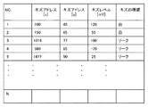
撮像素子103からは、例えば、その出荷時に所定の駆動、所定の電荷蓄積時間、所定の環境温度にて得られた画像データに基づいて、各種のキズ画素(欠陥画素)が抽出される。主な欠陥は温度や蓄積時間に依存する暗電流に起因するものであるが、それ以外にリーク電流に起因する欠陥もある。これらのキズ画素の抽出を低ビット分解能モードで行い、図5に示すような、アドレス、キズレベル、キズの種別からなるキズ画素データ(欠陥情報)を作成して、撮像装置100内のメモリに格納しておく。なお、キズ画素抽出処理は、撮像装置100の外部で行っても良いし、撮像装置100での撮影時に、撮影した画像データより行っても良い。すなわち、撮像素子103が単体の状態で行っても良いし、撮像素子103が撮像装置に組み込まれた状態で行っても良い。
For example, various defect pixels (defective pixels) are extracted from the
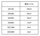
各種キズのうち、白キズに関しては、電荷蓄積時間や温度、また設定されたISO感度によって変わるため、撮影条件に応じて補正レベルを変更するのが望ましい。これは公知のキズ画素補正方法で実施可能である。 Among various scratches, white scratches vary depending on the charge accumulation time and temperature, and the set ISO sensitivity, so it is desirable to change the correction level according to the shooting conditions. This can be performed by a known defect pixel correction method.
一方、リークキズは上述したようにリーク電流に起因したキズである。ここで、補正対象となるリークキズを有するリークキズ画素を決定する処理について、図7のフローチャートに沿って説明する。なお、この補正対象となるリークキズ画素を決定する処理は全体制御・演算回路106で行い、その結果に応じて全体制御・演算回路106が補正対象のリークキズ画素を補正する。
On the other hand, the leakage scratch is a scratch caused by the leakage current as described above. Here, processing for determining a leak-scratched pixel having a leak-scratch to be corrected will be described with reference to the flowchart of FIG. The process of determining the leak-scratched pixel to be corrected is performed by the overall control /
まず、S11において、撮影時に設定されたビット分解能モードを取得し、S12において、撮影時の感度を取得する。次に、S13において、図5に示すキズ画素データから、キズの種類が「リーク」であるリークキズ画素のデータを1つ抽出する。図5のキズ画素データの例では、No.3、4、5がリークキズを有する画素である。
First, in S11, the bit resolution mode set at the time of shooting is acquired, and in S12, the sensitivity at the time of shooting is acquired. Next, in S13, one piece of leak-scratched pixel data whose type of “leak” is extracted from the scratch-pixel data shown in FIG. In the example of scratch pixel data in FIG.
そして、S14において、S11で取得したビット分解能モードが低ビット分解能モードであるかどうかを判別する。低ビット分解能モードであればS16に進み、図6のテーブルに従って、S13で抽出したキズレベルが、S12で取得した感度における補正レベル以上(閾値以上)であるかどうかを判断する。図6の補正レベル以上の場合、S17において抽出したリークキズ画素は補正対象であると決定して、当該情報を信号処理回路104に渡し、S18に進む。
In S14, it is determined whether or not the bit resolution mode acquired in S11 is the low bit resolution mode. If it is the low bit resolution mode, the process proceeds to S16, and it is determined whether the scratch level extracted in S13 is equal to or higher than the correction level (threshold value) in the sensitivity acquired in S12 according to the table of FIG. If it is equal to or higher than the correction level in FIG. 6, it is determined that the leaked defect pixel extracted in S17 is a correction target, the information is passed to the
一方、補正レベル未満(閾値未満)の場合は、直接S18に進んで、全てのリークキズ画素のデータに対して決定処理を行ったかを判断し、決定処理を行っていないリークキズ画素があれば、S13に戻って次のリークキズ画素のデータを1つ抽出する。全てのリークキズ画素のデータに対して決定処理が終了していれば、処理を終了する。 On the other hand, if it is less than the correction level (less than the threshold value), the process proceeds directly to S18 to determine whether the determination processing has been performed on the data of all the leak-scratched pixels. Returning to, one piece of data of the next leaked flaw pixel is extracted. If the determination process has been completed for all leaked pixel data, the process ends.
例えば、ISO400での撮影の場合、キズレベルの絶対値が32mV以上のキズ画素を補正する。即ち、図5のキズ画素データにおいては、No.3とNo.4のリークキズ画素は補正対象となり、No.5のリークキズ画素は補正対処とならない。 For example, in the case of shooting with ISO 400, a flaw pixel having an absolute value of a flaw level of 32 mV or more is corrected. That is, in the flaw pixel data of FIG. 3 and no. No. 4 leak flaw pixel is the correction target. The leak-scratched pixel of 5 is not corrected.
S14において高ビット分解能モードであればS15に進み、S13で抽出したキズレベルをS信号読み出し期間に応じて調整する。ここで、低ビット分解能モードでのS信号読み出し期間をT1、高ビット分解能モードでのS信号読み出し期間をT2とし(T1<T2)、低ビット分解能モードで抽出されたリークキズのキズレベルをL1とする。この場合、高ビット分解能モードでのリークキズのキズレベルL2は、
L2=T2/T1×L1×α …(1)
となる(αはT2/T1×α>1を満たす任意の係数)。このように、式(1)で算出されたキズレベルL2が、高ビット分解能モードでのリークキズのキズレベルとなる。キズレベルL2の算出後、S16において、図6のテーブルに従って、算出されたキズレベルL2が、S12で取得した感度における補正レベル以上であるかどうかを判断する。以降、上述したS17及びS18の処理を行う。
If the high bit resolution mode is selected in S14, the process proceeds to S15, and the scratch level extracted in S13 is adjusted according to the S signal readout period. Here, the S signal reading period in the low bit resolution mode is T1, the S signal reading period in the high bit resolution mode is T2 (T1 <T2), and the defect level of the leaked defect extracted in the low bit resolution mode is L1. . In this case, the scratch level L2 of the leak scratch in the high bit resolution mode is
L2 = T2 / T1 × L1 × α (1)
(Α is an arbitrary coefficient satisfying T2 / T1 × α> 1). In this way, the scratch level L2 calculated by the equation (1) is the leak scratch scratch level in the high bit resolution mode. After calculating the scratch level L2, in S16, it is determined whether or not the calculated scratch level L2 is equal to or higher than the correction level in the sensitivity acquired in S12. Thereafter, the processes of S17 and S18 described above are performed.
このように、S信号読み出し期間の長さに応じてキズレベルを換算して、リークキズ補正を行うかどうかを決定することで、過不足なくリークキズ画素の補正を行うことができる。また、それぞれのビット分解能モードに対応したキズ画素情報をメモリに格納する必要もないので、キズ画素の抽出時間の短縮、及び、撮像装置のメモリ削減も可能となる。 As described above, the defect level is converted according to the length of the S signal readout period, and it is determined whether or not the leak defect correction is performed, so that the leak defect pixel can be corrected without excess or deficiency. Further, since it is not necessary to store flaw pixel information corresponding to each bit resolution mode in the memory, it is possible to shorten the extraction time of flaw pixels and to reduce the memory of the imaging apparatus.
なお、全体制御・演算回路106におけるキズ画素の補正に関しては、公知の補間方法を用いて実施可能である。
It should be noted that the flaw pixel correction in the overall control /
以上のように、S信号読み出し期間の長さに応じて、キズ補正やノイズ低減処理のレベルを変えることで、精度良く適切なノイズ低減処理を実施することが可能となる。なお、本第1の実施形態で示したS信号読み出し期間の異なる駆動は一例であり、本発明はこれに限定されるものではない。 As described above, appropriate noise reduction processing can be performed with high accuracy by changing the level of defect correction or noise reduction processing according to the length of the S signal readout period. The driving with different S signal readout periods shown in the first embodiment is an example, and the present invention is not limited to this.
<変形例>
画像のキズ、及びノイズ補正としては、撮影された画像からキズ画素を検出して補正を行う、リアルタイムキズ補正方法がある。リアルタイムキズ補正も公知の技術であり、様々な手法が開示されているが、基本的には得られた画素の出力が周辺画素の信号に対して予め設定した閾値以上のレベル差があれば欠陥画素と判定し、キズ補正を実施するものである。
<Modification>
As image flaw and noise correction, there is a real-time flaw correction method in which a flaw pixel is detected from a captured image and correction is performed. Real-time scratch correction is also a well-known technique, and various methods have been disclosed. Basically, if the obtained pixel output has a level difference equal to or higher than a preset threshold with respect to the peripheral pixel signal, it is defective. The pixel is determined to be a pixel, and defect correction is performed.
図8はS信号読み出し期間T1、T2におけるダーク画像のヒストグラムであり、横軸が画素信号の出力、縦軸が累積頻度である。S信号読み出し期間T2のモードの方が、S信号読み出し期間T1のモードに比べてヒストグラムの分布が横に広がっており、画像としてノイズの多い状態となっている。これは、前述の通り、S信号−N信号処理の誤差がS信号読み出し期間T2の方で大きくなるためである。 FIG. 8 is a histogram of dark images in the S signal readout periods T1 and T2, where the horizontal axis represents the output of the pixel signal and the vertical axis represents the cumulative frequency. In the mode of the S signal readout period T2, the distribution of the histogram spreads horizontally compared to the mode of the S signal readout period T1, and the image is noisy. This is because, as described above, the error of the S signal-N signal processing becomes larger in the S signal readout period T2.
そこで、このノイズの差を考慮して、キズ判定閾値を、読み出しモード、すなわちS信号読み出し期間の長さに応じてレベルを変えて、リアルタイムキズ検出及び補正を行う。例えば、S信号読み出し期間T2となる高ビット分解能モードでのキズ判定に用いる閾値を、S信号読み出し期間T1となる低ビット分解能モードでのキズ判定に用いる閾値より低めに設定することで、補正後のノイズ量を同等とすることができる。 Therefore, in consideration of this noise difference, the level of the scratch determination threshold is changed according to the read mode, that is, the length of the S signal read period, and real-time scratch detection and correction are performed. For example, the threshold value used for the scratch determination in the high bit resolution mode during the S signal readout period T2 is set lower than the threshold value used for the scratch determination in the low bit resolution mode during the S signal readout period T1, so that The amount of noise can be made equal.
また、リアルタイムキズ補正だけでなく、その他のノイズ低減処理に関しても、処理の強さをS信号読み出し期間の長さに応じて変えることが望ましい。 In addition to the real-time scratch correction, it is desirable to change the strength of processing according to the length of the S signal readout period for other noise reduction processing.
また、本発明はFHDなどの動画モードにおいて、画像の画素数を低画素化して読み出すモードに対しても好適である。低画素化方法には3画素中1画素読み出す間引き方法や、3画素中2画素加算したり、3画素中3画素加算する加算方法がある。その際は、ノイズ低減処理のレベルは、同じ加算数の処理を行った場合において、S信号読み出し期間の長さに応じて変えることが好適である。 The present invention is also suitable for a mode in which the number of pixels of an image is reduced and read out in a moving image mode such as FHD. The pixel reduction method includes a thinning-out method of reading out one pixel out of three pixels, an addition method of adding two out of three pixels, or adding out three out of three pixels. In that case, it is preferable to change the level of the noise reduction processing in accordance with the length of the S signal readout period when processing of the same number of additions is performed.
<第2の実施形態>
次に、本発明の第2の実施形態について説明する。撮像装置100の全体的な構成は、図1を参照して説明したものと同様であるが、撮像素子103の構成が第1の実施形態において説明したものと異なる。以下、図9を参照して、本発明の第2の実施形態における撮像素子103の構成について説明する。
<Second Embodiment>
Next, a second embodiment of the present invention will be described. The overall configuration of the
第2の実施形態では、図9に示すように、マイクロレンズアレイを形成する個々のマイクロレンズ804に対応する構成を1つの画素と定義し、これを単位画素800とする。また、1つのマイクロレンズ804に対して複数のフォトダイオード(PD)が対応するように配置されている。なお、第2の実施形態では、単位画素800にはX軸方向に2つのPD801A及びPD801B(光電変換部)が配置されている場合について説明する。これに対応して、第2の実施形態における列回路1009は、3つのメモリを有する。このような単位画素800及び列回路1009が、図2に示す撮像素子103の構成において、単位画素200と列回路203の代わりに用いられる。
In the second embodiment, as shown in FIG. 9, a configuration corresponding to each
図10は、撮影レンズ903から出射された光が1つのマイクロレンズ804を通過してPD801A、801Bで受光される様子を、光軸Zに対して垂直方向(Y軸方向)から観察した図である。レンズ絞り904により制限され、射出瞳901、902を通過した光は、光軸Zを中心として単位画素800に入射する。図10に示すように射出瞳901を通過する光束はマイクロレンズ804を通して、PD801Aで受光され、射出瞳902を通過する光束はマイクロレンズ804を通して、PD801Bで受光される。したがって、PD801AとPD801Bはそれぞれ撮影レンズ903の射出瞳の異なる領域の光を受光している。
FIG. 10 is a diagram in which the light emitted from the photographing
このように瞳分割されたPD801Aから得られる信号をX軸方向に並ぶ複数の単位画素800から取得し、これらの出力信号群で構成した被写体像をA像とする。同様に瞳分割されたPD801Bの信号をX軸方向に並ぶ複数の単位画素800から取得し、これらの出力信号群で構成した被写体像をB像とする。A像とB像に対して相関演算を実施し、像のずれ量(瞳分割位相差)を検出し、さらに像のずれ量に対して撮影レンズ903の焦点位置と光学系から決まる変換係数を乗じることで、画面内の任意の被写体位置に対応した焦点位置を算出することができる。ここで算出された焦点位置情報に基づいて、撮影レンズ903のフォーカスを制御することで、撮像面位相差AFが可能となる。
A signal obtained from the pupil-divided
また、A像信号とB像信号とを足し合わせて得られたA+B像信号を、通常の撮影画像に用いることができる。 Further, an A + B image signal obtained by adding the A image signal and the B image signal can be used for a normal captured image.
図11は、第2の実施形態における撮像素子103の単位画素800の画素回路及び列回路1009の一例を示す図である。単位画素800において、PD801Aには転送スイッチ1002Aが接続され、PD801Bには転送スイッチ1002Bが接続される。PD801A、801Bで発生した電荷は、それぞれ転送スイッチ1002A、1002Bを介して共通のFD1004に転送され、一時的に保持される。FD304に転送された電荷は、選択スイッチ1006がオンされると、ソースフォロワアンプを形成する増幅MOSトランジスタ(SF)1005を介して電荷に対応した電圧として垂直出力線201に出力される。なお、選択スイッチ1006は行単位で制御され、選択された行の画素信号が一括して垂直出力線201に出力される。リセットスイッチ1003は、FD1004の電位、及び転送スイッチ1002A、及び1002Bを介してPD801A、801Bの電位をVDDにリセットする。転送スイッチ1002A、1002B、リセットスイッチ1003、選択スイッチ1006は、それぞれ垂直走査回路208に接続されている信号線を介して制御信号PTXA、PTXB、PRES、PSELにより制御される。
FIG. 11 is a diagram illustrating an example of the pixel circuit and the
次に、列回路1009の回路構成について説明する。なお、列回路1009は、第1の実施形態で説明した列回路203とほぼ同様の構成であるため、ここでは差異のみ説明する。上述したように、単位画素800は2つのPD801A、801Bを有し、後述する撮像面位相差AFを行うモード(撮像面位相差AFモード)においては、A像信号とA+B像信号をそれぞれ読み出す。そのため、第2の実施形態における列回路1009は、AD変換されたデジタル信号を保持するメモリを3つ備える。メモリ1015には、FD1004のリセット信号(以下、「N信号」)をAD変換したデジタル信号が保持される。メモリ1016には、PD801Aの信号をFD1004のN信号に重畳した信号(以下、「S(A)信号」)をAD変換したデジタル信号が保持される。そして、メモリ1017にはPD801A及びPD801Bの信号をFD1004のN信号に重畳した信号(以下「S(A+B)信号」)をAD変換したデジタル信号が保持される。メモリ1015に保持されたN信号は水平走査回路205からの制御信号によって、水平出力線216を介してデジタル出力処理回路207へ出力される。また、メモリ1016、1017に保持されたS(A)信号及びS(A+B)信号は、水平走査回路205からの信号によって、水平出力線217を介してデジタル出力処理回路207へ出力される。そして、デジタル出力処理回路207において、S(A)信号及びS(A+B)信号からN信号の差分が算出されて、ノイズの要因となるFD304のリセットノイズ成分が除去された信号が出力される。
Next, a circuit configuration of the
図12及び図13は、図11に示す回路構成を有する撮像素子103の1行分の単位画素800からの電荷読み出し動作の一例を示すタイミングチャートである。第2の実施形態における撮像素子103は、通常撮影モード(第1の駆動)と撮像面位相差AFモード(第2の駆動)を有し、図12が通常撮影モードのタイミングチャート、図13が撮像面位相差AFモードのタイミングチャートである。各駆動パルスのタイミング、参照電圧Vslope、CLK、水平走査信号を模式的に示している。また、各タイミングにおける、垂直出力線の電位Vlもあわせて示している。
12 and 13 are timing charts showing an example of a charge reading operation from the
まず、図12を参照しながら、通常撮影モードにおける電荷読み出し動作について説明する。なお、時刻t1107でAD変換されたN信号がメモリ1015に保持されるまでは、第1の実施形態で説明した図4の時刻t407までの駆動と同様なので、説明を省略する。
First, the charge reading operation in the normal photographing mode will be described with reference to FIG. Until the N signal subjected to AD conversion at the time t1107 is held in the
N信号読み出し期間が終了した後の時刻t1107、t1108で制御信号PTXA及びPTXBを順次Hi、LoとしてPD801A及びPD801Bに蓄積された光電荷をFD1004に転送する。すると、電荷量に応じたFD1004の電位変動が垂直出力線201にS(A+B)信号レベル(光成分+リセットノイズ成分(N信号))として読み出され、列回路1009に入力される。S(A+B)信号はアンプ1010で所望のゲインで増幅された後、時刻t1109、t1110で制御信号PSHを順次Hi、Loとしてスイッチ1011がオン、オフされるタイミングで容量1012に保持される。容量1012に保持された電位は比較器1013の一方に入力される。時刻t1110でスイッチ1011がオフされた後、時刻t1111からt1113まで、スロープ電圧発生回路204により、参照電圧Vslopeを時刻と共に初期値から減少させていく。参照電圧Vslopeの遷移開始と共に、CLKをカウンタ1014に供給する。CLKの数に応じてカウンタ1014の値は増加していく。そして、比較器1013に入力した参照電圧VslopeがS(A+B)信号と同じレベルになると、比較器1013の出力COMPはローレベルとなり、同時にカウンタ1014の動作も停止する(時刻t1112)。この、カウンタ1014の動作が停止した時の値が、S(A+B)信号がAD変換された値となり、S(A+B)信号用メモリ1017に保持される。ここで、時刻t1104からt1110までの期間T3がS(A+B)信号読み出し期間となる。
At times t1107 and t1108 after the end of the N signal read period, the control signals PTXA and PTXB are sequentially set to Hi and Lo, and the photocharges accumulated in the
続いて、メモリ1015、1017に保持された信号を水平走査回路205により読み出す。時刻t1113より、列回路1009ごとに順次動作させることでメモリ1015、1017に保持された信号は水平出力線216、217を通り、デジタル出力処理回路207に送られ、そこで差動信号レベル(光成分)が算出される。
Subsequently, the signals held in the
このように、制御信号PTXAとPTXBを同時にオンすることにより、PD801A、801Bに蓄積された電荷を同時にFD1004に転送して撮像信号を読み出すことができる。
In this way, by simultaneously turning on the control signals PTXA and PTXB, the charges accumulated in the
続いて、図13を参照しながら、撮像面位相差AFモードにおける電荷読み出しについて説明する。撮像面位相差AFモードでは、AF用の情報と撮像用の情報の両方を取得することができる。 Next, charge readout in the imaging plane phase difference AF mode will be described with reference to FIG. In the imaging plane phase difference AF mode, both AF information and imaging information can be acquired.
撮像面位相差AFモードにおいても、時刻t1207でAD変換されたN信号がメモリ1015に保持されるまでは、第1の実施形態で説明した図4の時刻t407までの駆動と同様なので、説明を省略する。
Even in the imaging plane phase difference AF mode, until the N signal subjected to AD conversion at time t1207 is held in the
N信号読み出し期間が終了した後の時刻t1207、t1208で制御信号PTXAを順次Hi、LoとしてPD801Aに蓄積された光電荷をFD1004に転送する。すると、電荷量に応じたFD1004の電位変動が垂直出力線201にS(A)信号レベル(光成分+リセットノイズ成分(N信号))として読み出され、列回路1009に入力される。S(A)信号はアンプ1010で所望のゲインで増幅されたのち、時刻t1209、t1210で制御信号PSHを順次Hi、Loとしてスイッチ1011がオン、オフされるタイミングで容量1012に保持される。容量1012に保持された電位は比較器1013の一方に入力される。時刻t1210でスイッチ1011がオフされた後、時刻t1211からt1213まで、スロープ電圧発生回路204により、参照電圧Vslopeを時刻と共に初期値から減少させていく。参照電圧Vslopeの遷移開始と共に、CLKをカウンタ1014に供給する。CLKの数に応じてカウンタ1014の値は増加していく。そして、比較器1013に入力した参照電圧VslopeがS(A)信号と同じレベルになると、比較器1013の出力撮像面位相差AFはローレベルとなり、同時にカウンタ1014の動作も停止する(時刻t1212)。この、カウンタ1014の動作が停止した時の値が、S(A)信号がAD変換された値となり、S(A)信号用メモリ1016に保持される。
At times t1207 and t1208 after the end of the N signal readout period, the control signal PTXA is sequentially set to Hi and Lo, and the photocharge accumulated in the
続いて、時刻t1213、t1214で制御信号PTXA、PTXBを順次Hi、LoとしてPD801A及びPD801Bに蓄積された光電荷をFD1004に転送する。すると、電荷量に応じたFD1004の電位変動が垂直出力線201にS(A+B)信号レベル(光成分+リセットノイズ成分(N信号))として読み出され、列回路1009に入力される。S(A+B)信号はアンプ1010で所望のゲインで増幅された後、時刻t1215、t1216で制御信号PSHを順次Hi、Loとしてスイッチ1011をオン、オフされるタイミングで容量1012に保持される。容量1012に保持された電位は比較器1013の一方に入力される。時刻t1216でスイッチ1011がオフされた後、時刻t1217からt1219まで、スロープ電圧発生回路204により、参照電圧Vslopeを時刻と共に初期値から減少させていく。参照電圧Vslopeの遷移開始と共に、CLKをカウンタ1014に供給する。CLKの数に応じてカウンタ1014の値は増加していく。そして、比較器1013に入力した参照電圧VslopeがS(A)信号と同じレベルになると、比較器1013の出力COMPはローレベルとなり、同時にカウンタ1014の動作も停止する(時刻t1218)。この、カウンタ1014の動作が停止した時の値が、S(A+B)信号がAD変換された値となり、S(A+B)信号用メモリ1017に保持される。ここで、時刻t1204からt1216までが、N信号が容量1012に保持されてから、S(A+B)信号が容量1012に保持される時間であり、S(A+B)信号読み出し期間となる。
Subsequently, at times t1213 and t1214, the control signals PTXA and PTXB are sequentially set to Hi and Lo to transfer the photocharges accumulated in the
続いて、メモリ1015、1016、1017に保持された信号を水平走査回路205により読み出す工程について説明する。S(A)信号が読み出された後の時刻t1213より、列回路1009ごとに順次動作させることでメモリ1015、1016に保持された信号は水平出力線216、217を通り、デジタル出力処理回路207に送られる。そして、差動信号レベル(A像の光成分)が算出される。また、S(A+B)信号が読み出された後の時刻t1219より、列回路1009ごとに順次動作させることでメモリ1015、1017に保持された信号は水平出力線216、217を通り、デジタル出力処理回路207に送られる。そして、そこで差動信号レベル(撮像画像の光成分)が算出される。
Next, a process of reading signals held in the
このように、最初に制御信号PTXAのみオンしてA像信号を読み出し、その後、制御信号PTXAとPTXBを同時にオンして撮像信号(A+B像信号)を読み出すことにより、AF用の情報と撮像用の情報の両方を取得することができる。なお、AF用のB像信号はA+B像信号からA像信号を減算することにより算出することができる。この処理は、信号処理回路104で行っても良いし、全体制御・演算回路106で行っても良い。
Thus, only the control signal PTXA is first turned on to read the A image signal, and then the control signals PTXA and PTXB are turned on at the same time to read the imaging signal (A + B image signal). Both information can be obtained. The B image signal for AF can be calculated by subtracting the A image signal from the A + B image signal. This processing may be performed by the
撮像装置100は、シーンや用途に応じて通常撮影モードと撮像面位相差AFモードを使い分けることができる。この時、N信号(リセット信号)を読み出した時刻から撮像用信号(A+B像信号)が読み出されるまでの時間は、通常撮影モード(T3)と撮像面位相差AFモード(T4)とで異なる。T4の方が、A像信号読み出しを行っている分長くなる。ここで課題となってくるのが、第1の実施形態で説明したようにリーク電流の影響によるノイズ差である。
The
そこで、第1の実施形態と同様に、撮像用信号が読み出されるまでの時間に応じて補正対象とするキズ補正のレベルや、ノイズ低減処理の強さを変えることで解決することができる。例えば、図7を参照して説明した処理において、S11でビット分可能モードを取得する代わりに撮影モードを取得し、S14において取得した撮影モードが通常撮影モードであるか否かを判断する。そして、撮像面位相差AFモードの場合に、以下の式(2)によりキズレベルを調整することで、補正対象の画素であるか否かを決定することができる。通常撮影モードで抽出されたリークキズのレベルをL3とすると、撮像面位相差AFモードでのリークキズレベルL4を、
L4=T4/T3×L3×α …(2)
により求める(αはT4/T3×α>1を満たす任意の係数)。
Therefore, similarly to the first embodiment, the problem can be solved by changing the level of the defect correction to be corrected and the strength of the noise reduction process according to the time until the imaging signal is read. For example, in the processing described with reference to FIG. 7, the shooting mode is acquired instead of acquiring the bit possible mode in S11, and it is determined whether or not the shooting mode acquired in S14 is the normal shooting mode. In the case of the imaging plane phase difference AF mode, it is possible to determine whether or not the pixel is a correction target pixel by adjusting the scratch level according to the following equation (2). When the level of leak scratches extracted in the normal shooting mode is L3, the leak scratch level L4 in the imaging surface phase difference AF mode is
L4 = T4 / T3 × L3 × α (2)
(Α is an arbitrary coefficient satisfying T4 / T3 × α> 1).
また、リアルタイムキズ補正やその他のノイズ低減処理に関しても、処理の強さをS信号読み出し期間の長さに応じて変えることで、低ノイズの撮影画像を得ることができる。 Also, with regard to real-time scratch correction and other noise reduction processing, a low-noise captured image can be obtained by changing the strength of processing according to the length of the S signal readout period.
以上のように、焦点検出が行える構成の撮像素子を備えた撮像装置においても、S信号読み出し期間の長さに応じて、キズ補正やノイズ低減処理のレベルを変えることで、精度良く適切なノイズ低減処理を実施することが可能となる。 As described above, even in an image pickup apparatus including an image pickup device configured to perform focus detection, appropriate noise can be accurately obtained by changing the level of scratch correction or noise reduction processing according to the length of the S signal readout period. Reduction processing can be performed.
なお、上述した例では、全ての画素が図9に示す構成を有するものとして説明したが、本発明はこれに限るものではなく、少なくとも一部の画素を図9に示す構成とすることで、撮像面位相差AFを行うことが可能である。 In the example described above, all the pixels have been described as having the configuration shown in FIG. 9, but the present invention is not limited to this, and at least some of the pixels have the configuration shown in FIG. Imaging surface phase difference AF can be performed.
<第3の実施形態>
次に、本発明の第3の実施形態について説明する。第2の実施形態において、図11に示す撮像素子103の駆動方法について2つのモードを説明した。撮像面位相差AFモードにおいては、AF用の情報と撮像用の情報の両方を取得可能であるが、A像信号を読み出してから、A+B像信号を読み出すため、通常撮影モードに比べて1枚の画像取得に必要な読み出し時間が長くなりフレームレートが下がってしまう。
<Third Embodiment>
Next, a third embodiment of the present invention will be described. In the second embodiment, two modes have been described for the driving method of the
そこで、1フレームにおいて、撮像面位相差AFモードで読み出す行と通常撮影モードで読み出す行を混在させれば、フレームレートを大きく落とすことなくAF用情報を得ることが可能である。以下、このモードを行選択的撮像面位相差AFモードと呼ぶ。 Therefore, in one frame, if the rows read in the imaging plane phase difference AF mode and the rows read in the normal photographing mode are mixed, it is possible to obtain AF information without greatly reducing the frame rate. Hereinafter, this mode is referred to as a row selective imaging plane phase difference AF mode.
図14は、撮像素子103の画素領域における、行選択的撮像面位相差AFモードでの読み出し方の一例を示す図である。各行における読み出しモードを示しており、ここでは4行のうち1行をAF用情報を取得するために撮像面位相差AFモードで読み出す駆動とし、その他の3行を通常撮影モードで読み出す駆動としている。このように、行単位で所定の割合で、撮像面位相差AFモードと通常撮影モードとによる読み出しを交互に行う。
FIG. 14 is a diagram illustrating an example of how to read in the row selective imaging surface phase difference AF mode in the pixel region of the
通常読み出しモード、撮像面位相差AFモードそれぞれの駆動は、第2の実施形態で説明した図12、図13のタイミングチャートと同様に駆動することで実施可能である。 Each of the normal readout mode and the imaging plane phase difference AF mode can be driven by driving in the same manner as the timing charts of FIGS. 12 and 13 described in the second embodiment.
図14に示したような行選択的撮像面位相差AFモードの場合、1フレーム内で行によってS信号読み出し期間の長さが異なることになる。すなわち、リーク電流の影響により、行によってノイズ差が出てしまい、ノイズ差が大きい場合は、横縞ノイズとなって画質劣化の要因となってしまう。 In the case of the row selective imaging surface phase difference AF mode as shown in FIG. 14, the length of the S signal readout period differs depending on the row within one frame. That is, due to the influence of the leak current, a noise difference is generated depending on the row, and when the noise difference is large, horizontal stripe noise becomes a factor in image quality degradation.
そこで、第3の実施形態においては、1フレーム内の通常撮影モード行と撮像面位相差AFモード行とで、キズ補正のレベルや、ノイズ低減処理の強さを変える。撮影時に予め、どの行がどのモードで信号読み出しを行うかを記憶しておき、その情報に応じてキズ補正のレベルやノイズ低減処理の強さを変えることで実施可能である。 Therefore, in the third embodiment, the level of defect correction and the strength of noise reduction processing are changed between the normal shooting mode row and the imaging plane phase difference AF mode row in one frame. This can be implemented by storing which line performs signal readout in which mode in advance, and changing the level of flaw correction and the strength of noise reduction processing according to the information.
以上のように、1フレーム内で行によってS信号読み出し期間が異なる駆動となる行選択的撮像面位相差AFモード駆動において、S信号読み出し期間の長さに応じて、キズ補正やノイズ低減処理のレベルを変えることで、精度良く適切なノイズ低減処理を実施することが可能となる。 As described above, in row-selective imaging surface phase difference AF mode driving in which the S signal readout period differs depending on the row in one frame, the scratch correction and noise reduction processing are performed according to the length of the S signal readout period. By changing the level, it is possible to accurately perform appropriate noise reduction processing.
100:撮像装置、101:撮像レンズ、103:撮像素子、104:信号処理回路、105:タイミング発生回路、106:全体制御・演算回路、203:列回路、204:スロープ電圧発生回路、207:デジタル出力処理回路、301、801A、801B::フォトダイオード(PD)、313、1013:比較器、314、1014:カウンタ、315、316、1015、1016、1017:メモリ
DESCRIPTION OF SYMBOLS 100: Imaging device, 101: Imaging lens, 103: Image sensor, 104: Signal processing circuit, 105: Timing generation circuit, 106: Overall control / arithmetic circuit, 203: Column circuit, 204: Slope voltage generation circuit, 207: Digital
Claims (11)
前記撮像素子が、
複数のマイクロレンズと、
前記複数のマイクロレンズそれぞれに、少なくとも1つの光電変換部が対応するように構成された複数の光電変換部と、
前記複数の光電変換部から撮像信号を読み出す読み出し手段と、
読み出された撮像信号を保持するメモリとを有し、
前記撮像素子は、前記読み出し手段が前記複数の光電変換部に蓄積された撮像信号を読み出して前記メモリに保持するまでの信号読み出し期間が異なる、少なくとも2つ以上の駆動方法により駆動され、
前記画像処理手段は、前記読み出された撮像信号のノイズを低減するノイズ低減処理を行うノイズ低減手段を備え、該ノイズ低減手段は、前記読み出された撮像信号のうち、前記ノイズ低減処理を行う撮像信号を判定して前記ノイズ低減処理を行い、該判定を行う際に、前記信号読み出し期間の異なる2つ以上の駆動方法において該判定のレベルを調整することを特徴とする撮像装置。 An image pickup apparatus having an image pickup element and image processing means for processing a signal read from the image pickup element to generate an image,
The image sensor is
A plurality of microlenses,
A plurality of photoelectric conversion units configured such that at least one photoelectric conversion unit corresponds to each of the plurality of microlenses;
A reading means for reading an imaging signal from the plurality of photoelectric conversion units;
A memory for holding the read imaging signal;
The imaging element is driven by at least two or more driving methods in which a signal readout period from when the readout unit reads out an imaging signal accumulated in the plurality of photoelectric conversion units and holds it in the memory is different,
Said image processing means comprises noise reduction means for performing noise reduction processing for reducing noise in the read out image signal, said noise reducing means, among the read out by the imaging signal, the noise reduction processing An imaging apparatus comprising: determining an imaging signal to be performed, performing the noise reduction processing, and adjusting the determination level in two or more driving methods having different signal readout periods when performing the determination .
前記ノイズ低減手段は、前記信号読み出し期間に応じて前記欠陥のレベルが変わる種類の欠陥に対して、前記予め決められた条件における信号読み出し期間と、前記撮像信号の読み出しにかかった信号読み出し期間との比に応じて、前記欠陥のレベルを調整することを特徴とする請求項1または2に記載の撮像装置。 When photographing is performed under a predetermined condition, there is further provided a storage means for previously storing defect information including an address of a photoelectric conversion unit corresponding to an imaging signal in which a defect appears, a defect type, and a defect level. And
The noise reduction means includes a signal readout period under the predetermined condition and a signal readout period required for readout of the imaging signal for a type of defect whose level of the defect changes according to the signal readout period. The image pickup apparatus according to claim 1, wherein a level of the defect is adjusted in accordance with a ratio.
前記読み出し手段は、前記撮像信号に先立って前記撮像素子からリセットレベルの信号を読み出して前記メモリに保持し、前記変換手段により前記保持されたリセットレベルの信号の変換が終了してから、前記撮像信号の読み出しを開始することを特徴とする請求項1乃至5のいずれか1項に記載の撮像装置。 Further comprising conversion means for analog-to-digital conversion of the signal held in the memory;
The readout means reads out a reset level signal from the image sensor prior to the imaging signal and holds the reset level signal in the memory. After the conversion of the reset level signal held by the conversion means is completed, the imaging 6. The image pickup apparatus according to claim 1, wherein reading of a signal is started.
前記ノイズ低減手段は、前記加算数が同じで、かつ前記信号読み出し期間の長さが異なる場合に、前記判定のレベルを調整することを特徴とする請求項1乃至7のいずれか1項に記載の撮像装置。 The readout means adds and reads out the imaging signals of the plurality of photoelectric conversion units by a predetermined number,
The said noise reduction means adjusts the level of the said determination, when the said addition number is the same and the length of the said signal read-out period differs, The said determination level is characterized by the above-mentioned. Imaging device.
前記駆動方法は、前記各マイクロレンズに対応する前記複数の光電変換部からの前記撮像信号を加算して読み出す第1の駆動方法と、前記複数の光電変換部それぞれの前記撮像信号を取得可能に読み出す第2の駆動方法とを含み、
前記第1の駆動方法よりも、前記第2の駆動方法による前記信号読み出し期間が長いことを特徴とする請求項1乃至7のいずれか1項に記載の撮像装置。 The imaging device is configured such that a plurality of photoelectric conversion units correspond to at least some of the microlenses of the plurality of microlenses,
The driving method, the first driving method of adding and reading the imaging signals from the plurality of photoelectric conversion units corresponding to each microlens, capable acquires the image signal of each of the plurality of photoelectric conversion unit A second driving method of reading,
8. The imaging apparatus according to claim 1, wherein the signal readout period according to the second driving method is longer than that of the first driving method.
前記撮像素子は、前記読み出し手段が前記複数の光電変換部に蓄積された撮像信号を読み出して前記メモリに保持するまでの信号読み出し期間が異なる、少なくとも2つ以上の駆動方法により駆動され、前記画像処理手段は、前記読み出された撮像信号のノイズを低減するノイズ低減処理を行うノイズ低減手段を備え、
前記ノイズ低減手段が、前記撮像信号の読み出しに用いられた駆動方法による信号読み出し期間を取得する取得工程と、
前記ノイズ低減手段が、前記信号読み出し期間の異なる2つ以上の駆動方法において、前記読み出された撮像信号のうち、前記ノイズ低減処理を行う撮像信号を判定するレベルを調整する調整工程と、
前記調整されたレベルに応じて前記ノイズ低減処理を行う撮像信号を判定する判定工程と
を有することを特徴とする撮像装置の制御方法。 A plurality of microlenses, a plurality of photoelectric conversion units configured so that at least one photoelectric conversion unit corresponds to each of the plurality of microlenses, and a reading unit that reads an imaging signal from the plurality of photoelectric conversion units; An image pickup apparatus control method comprising: an image pickup device having a memory that holds a read image pickup signal; and an image processing unit that processes the signal read from the image pickup device to generate an image.
The image sensor is driven by at least two or more driving methods in which a signal readout period from when the readout unit reads out an imaging signal accumulated in the plurality of photoelectric conversion units to hold in the memory is different, and the image processing means comprises noise reduction means for performing noise reduction processing for reducing noise in the read out image signal,
An acquisition step of said noise reducing means acquires by that signal readout period in the driving method used for reading the image signal,
Said noise reducing means, in two or more driving method having the different signal readout period, among the read out by the imaging signal, an adjustment step of adjusting the level for determining the imaging signal for the noise reduction processing,
And a determination step of determining an imaging signal for performing the noise reduction processing in accordance with the adjusted level.
Priority Applications (1)
| Application Number | Priority Date | Filing Date | Title |
|---|---|---|---|
| JP2014138019A JP6355459B2 (en) | 2014-07-03 | 2014-07-03 | Imaging apparatus and control method thereof |
Applications Claiming Priority (1)
| Application Number | Priority Date | Filing Date | Title |
|---|---|---|---|
| JP2014138019A JP6355459B2 (en) | 2014-07-03 | 2014-07-03 | Imaging apparatus and control method thereof |
Publications (3)
| Publication Number | Publication Date |
|---|---|
| JP2016015695A JP2016015695A (en) | 2016-01-28 |
| JP2016015695A5 JP2016015695A5 (en) | 2017-08-10 |
| JP6355459B2 true JP6355459B2 (en) | 2018-07-11 |
Family
ID=55231561
Family Applications (1)
| Application Number | Title | Priority Date | Filing Date |
|---|---|---|---|
| JP2014138019A Active JP6355459B2 (en) | 2014-07-03 | 2014-07-03 | Imaging apparatus and control method thereof |
Country Status (1)
| Country | Link |
|---|---|
| JP (1) | JP6355459B2 (en) |
Families Citing this family (5)
| Publication number | Priority date | Publication date | Assignee | Title |
|---|---|---|---|---|
| JP6736329B2 (en) * | 2016-03-31 | 2020-08-05 | キヤノン株式会社 | Image sensor |
| JP6765859B2 (en) | 2016-05-31 | 2020-10-07 | キヤノン株式会社 | Imaging device and its control method |
| JP6701001B2 (en) * | 2016-06-22 | 2020-05-27 | キヤノン株式会社 | Imaging device, control method thereof, program, and storage medium |
| JP2018148263A (en) * | 2017-03-01 | 2018-09-20 | ソニーセミコンダクタソリューションズ株式会社 | Solid-state image pickup device and electronic apparatus |
| JP7250428B2 (en) * | 2018-03-22 | 2023-04-03 | キヤノン株式会社 | Imaging device and its control method |
Family Cites Families (6)
| Publication number | Priority date | Publication date | Assignee | Title |
|---|---|---|---|---|
| JP3927702B2 (en) * | 1998-09-24 | 2007-06-13 | キヤノン株式会社 | Image processing apparatus, automatic focus detection apparatus, correction apparatus, correction method, and storage medium |
| JP4977541B2 (en) * | 2007-07-18 | 2012-07-18 | 富士フイルム株式会社 | Digital camera and operation control method thereof |
| JP5153563B2 (en) * | 2008-10-21 | 2013-02-27 | キヤノン株式会社 | Solid-state imaging device and driving method thereof |
| JP5742313B2 (en) * | 2011-03-10 | 2015-07-01 | 株式会社ニコン | Imaging device |
| JP5893572B2 (en) * | 2012-03-01 | 2016-03-23 | キヤノン株式会社 | Imaging device, imaging system, and driving method of imaging device |
| JP5968146B2 (en) * | 2012-07-31 | 2016-08-10 | キヤノン株式会社 | Solid-state imaging device and camera |
-
2014
- 2014-07-03 JP JP2014138019A patent/JP6355459B2/en active Active
Also Published As
| Publication number | Publication date |
|---|---|
| JP2016015695A (en) | 2016-01-28 |
Similar Documents
| Publication | Publication Date | Title |
|---|---|---|
| US9894295B2 (en) | Imaging device and imaging system | |
| US10038868B2 (en) | Solid-state image sensing device and electronic device | |
| US9531972B2 (en) | Solid-state imaging device, method for driving the same, and imaging device | |
| JP5852324B2 (en) | Imaging apparatus, control method therefor, and program | |
| WO2017047010A1 (en) | Image sensor and image capturing apparatus | |
| JP5312246B2 (en) | Imaging apparatus and control method | |
| US20140192249A1 (en) | Image capturing apparatus and method for controlling the same | |
| US20130070129A1 (en) | Image capturing apparatus and defective pixel detection method | |
| JP6602109B2 (en) | Control device, imaging device, control method, program, and storage medium | |
| JP6355459B2 (en) | Imaging apparatus and control method thereof | |
| US10630912B2 (en) | Image sensor, image capturing apparatus, and method for controlling image sensor | |
| JP2010245891A (en) | Imaging device and imaging method | |
| US8169524B2 (en) | Image sensing apparatus with pixel readout correction | |
| US10277855B2 (en) | Image sensing device and control method thereof with switchable analog-to-digital conversion modes based on the amount of dark current generated in pixels | |
| US20180295307A1 (en) | Image sensing apparatus and control method therefor | |
| JP2008017100A (en) | Solid-state imaging device | |
| JP2008148082A (en) | Solid-state imaging apparatus | |
| JP2016167773A (en) | Imaging apparatus and processing method of the same | |
| JP2008118571A (en) | Imaging apparatus and its control method | |
| JP2020057892A (en) | Imaging device | |
| US10368020B2 (en) | Image capturing apparatus and control method therefor | |
| JP2018133685A (en) | Imaging device, control method of the same, control program, and imaging apparatus | |
| JP2021072529A (en) | Imaging apparatus and control method of the same | |
| JP2019186817A (en) | Solid state image sensor, imaging apparatus, and control method of solid state image sensor | |
| JP2010141392A (en) | Solid-state image pickup device |
Legal Events
| Date | Code | Title | Description |
|---|---|---|---|
| A521 | Request for written amendment filed |
Free format text: JAPANESE INTERMEDIATE CODE: A523 Effective date: 20170630 |
|
| A621 | Written request for application examination |
Free format text: JAPANESE INTERMEDIATE CODE: A621 Effective date: 20170630 |
|
| A977 | Report on retrieval |
Free format text: JAPANESE INTERMEDIATE CODE: A971007 Effective date: 20180427 |
|
| TRDD | Decision of grant or rejection written | ||
| A01 | Written decision to grant a patent or to grant a registration (utility model) |
Free format text: JAPANESE INTERMEDIATE CODE: A01 Effective date: 20180514 |
|
| A61 | First payment of annual fees (during grant procedure) |
Free format text: JAPANESE INTERMEDIATE CODE: A61 Effective date: 20180612 |
|
| R151 | Written notification of patent or utility model registration |
Ref document number: 6355459 Country of ref document: JP Free format text: JAPANESE INTERMEDIATE CODE: R151 |