JP6286857B2 - Lighting lamp and lighting device - Google Patents
Lighting lamp and lighting device Download PDFInfo
- Publication number
- JP6286857B2 JP6286857B2 JP2013082418A JP2013082418A JP6286857B2 JP 6286857 B2 JP6286857 B2 JP 6286857B2 JP 2013082418 A JP2013082418 A JP 2013082418A JP 2013082418 A JP2013082418 A JP 2013082418A JP 6286857 B2 JP6286857 B2 JP 6286857B2
- Authority
- JP
- Japan
- Prior art keywords
- substrate
- electrode
- light emitting
- illumination lamp
- tube
- Prior art date
- Legal status (The legal status is an assumption and is not a legal conclusion. Google has not performed a legal analysis and makes no representation as to the accuracy of the status listed.)
- Active
Links
- 239000000758 substrate Substances 0.000 claims description 127
- 238000005286 illumination Methods 0.000 claims description 60
- 238000003466 welding Methods 0.000 claims description 6
- 230000002093 peripheral effect Effects 0.000 claims description 4
- 238000009826 distribution Methods 0.000 description 36
- 238000012986 modification Methods 0.000 description 25
- 230000004048 modification Effects 0.000 description 25
- 239000000463 material Substances 0.000 description 24
- 238000000034 method Methods 0.000 description 21
- 230000000052 comparative effect Effects 0.000 description 16
- 239000011521 glass Substances 0.000 description 7
- 238000010586 diagram Methods 0.000 description 6
- 229910052751 metal Inorganic materials 0.000 description 6
- 239000002184 metal Substances 0.000 description 6
- 239000011347 resin Substances 0.000 description 6
- 229920005989 resin Polymers 0.000 description 6
- 238000004088 simulation Methods 0.000 description 6
- 230000000694 effects Effects 0.000 description 5
- 238000004519 manufacturing process Methods 0.000 description 5
- 229910000679 solder Inorganic materials 0.000 description 5
- OAICVXFJPJFONN-UHFFFAOYSA-N Phosphorus Chemical compound [P] OAICVXFJPJFONN-UHFFFAOYSA-N 0.000 description 4
- 230000003287 optical effect Effects 0.000 description 4
- 239000000853 adhesive Substances 0.000 description 3
- 230000001070 adhesive effect Effects 0.000 description 3
- 238000007789 sealing Methods 0.000 description 3
- 238000005516 engineering process Methods 0.000 description 2
- 230000006872 improvement Effects 0.000 description 2
- 150000002739 metals Chemical class 0.000 description 2
- 230000009467 reduction Effects 0.000 description 2
- 239000007787 solid Substances 0.000 description 2
- 230000006641 stabilisation Effects 0.000 description 2
- 238000011105 stabilization Methods 0.000 description 2
- 239000013585 weight reducing agent Substances 0.000 description 2
- 238000004364 calculation method Methods 0.000 description 1
- 238000004140 cleaning Methods 0.000 description 1
- 238000013461 design Methods 0.000 description 1
- 238000009792 diffusion process Methods 0.000 description 1
- 239000007772 electrode material Substances 0.000 description 1
- 230000007613 environmental effect Effects 0.000 description 1
- 230000004907 flux Effects 0.000 description 1
- 230000017525 heat dissipation Effects 0.000 description 1
- 238000009434 installation Methods 0.000 description 1
- 238000012545 processing Methods 0.000 description 1
- 230000001737 promoting effect Effects 0.000 description 1
- 238000012827 research and development Methods 0.000 description 1
- 238000004381 surface treatment Methods 0.000 description 1
Images


Description
本発明は、照明ランプおよび照明装置に関し、特にLED(発光ダイオード)などの固体発光素子を発光手段とする照明ランプおよび照明装置に関する。 The present invention relates to an illumination lamp and an illuminating device, and more particularly to an illumination lamp and an illuminating device using a solid light emitting element such as an LED (light emitting diode) as a light emitting means.
従来、例えば下記の特許文献1に開示されているように、直管形LEDランプの配光特性を改善する(広配光角化)技術の研究開発が進められている。特許文献1は、LEDチップの発光面からの光が筒型の管表面から有効に出ていないことを解決することを課題としている。その解決策として、LEDチップから出る光を有効にガラス管外に出すために、その発光面の向きを管内面に垂直または垂直に近い角度になるようにしている。 Conventionally, for example, as disclosed in Patent Document 1 below, research and development of a technique for improving the light distribution characteristics of a straight tube LED lamp (wide light distribution angle) has been advanced. Patent document 1 makes it a subject to solve that the light from the light emission surface of a LED chip has not come out effectively from a cylindrical tube surface. As a solution, in order to effectively emit light emitted from the LED chip to the outside of the glass tube, the direction of the light emitting surface is set to be perpendicular or nearly perpendicular to the inner surface of the tube.
また、例えば下記の特許文献2、3、4に開示されているように、直管形LEDランプの放熱や軽量化の促進、組立て性の改善などを目的とした構成や構造に関して、いくつかの技術が公知である。
In addition, as disclosed in, for example,
LED(発光ダイオード)などの固体発光素子を発光手段とする照明ランプでは、透光性を備えた筒管の内部に発光部が設けられる。この発光部は、発光素子、およびこれを実装した基板で構成されるものである。 In an illumination lamp using a solid light emitting element such as an LED (light emitting diode) as a light emitting means, a light emitting portion is provided inside a light-transmitting tube. The light emitting unit includes a light emitting element and a substrate on which the light emitting element is mounted.
筒管内部における発光素子の位置は、配光性に直接の影響を与える。また、筒管の内径との関係や発光素子の実装構造との関係から一定の制約はあるものの、材料費の観点および基板による遮光面積の観点からは、基板は小型であることが好ましい。この点、筒管内部における発光部の構成に関して、上記従来の技術には広配光特性および経済性の観点からいまだ改善の余地があった。 The position of the light emitting element inside the tube has a direct influence on the light distribution. Further, although there are certain restrictions from the relationship with the inner diameter of the tube and the relationship with the mounting structure of the light emitting element, the substrate is preferably small from the viewpoint of material cost and the light shielding area by the substrate. In this regard, with respect to the configuration of the light emitting portion inside the tube, there is still room for improvement in the above-described conventional technology from the viewpoint of wide light distribution characteristics and economy.
本発明は、上述のような課題を解決するためになされたもので、高い広配光特性と経済性を兼ね備えた照明ランプおよび照明装置を提供することを目的とする。 The present invention has been made to solve the above-described problems, and an object of the present invention is to provide an illumination lamp and an illumination device having both high light distribution characteristics and economy.
本発明にかかる照明ランプは、
発光部と、
前記発光部を内部に収納し、前記発光部から出射される光を透過する筒管と、
を備え、
前記発光部は、
前記筒管の中心軸の側を向く表面に基板電極を備える基板と、
前記基板電極に実装された発光素子と、
を備え、
前記発光素子は、LEDチップを含む発光素子本体と、前記発光素子本体における前記基板電極と対向する裏面に設けられた素子電極と、を備えており、
前記発光素子は、前記LEDチップの平面視において、互いに直行する第一幅及び第二幅を備え、
前記第一幅の方向軸と平行な面で切断したときの断面視において、前記素子電極は、前記発光素子本体の前記裏面と重なる実装部と、前記実装部の外周端から前記発光素子本体の下側方向へ延び前記発光素子の側面を構成し前記発光素子の外部に露出された側面部と、前記側面部の下方端部から前記発光素子本体の下方領域の内側に伸び前記基板電極に重なる先端部と、を含むコの字の形状を有し、
前記LEDチップは、前記素子電極の前記実装部に実装され、
前記発光素子本体は、前記LEDチップを覆う封止樹脂を含み、
前記平面視において、前記素子電極および前記基板電極は、前記発光素子本体の前記裏面の面内に収まる大きさに設けられており、
前記平面視において、前記素子電極の外形の大きさと前記発光素子本体の前記裏面の外形の大きさとが同じであり、
前記基板は、前記筒管の内径よりも小さな幅を備え、前記中心軸から前記筒管の内面側に偏らせて配置されたことを特徴とする。
The illumination lamp according to the present invention is
A light emitting unit;
A cylindrical tube that houses the light emitting unit therein and transmits light emitted from the light emitting unit;
With
The light emitting portion,
A substrate Ru with a board electrode on the surface facing the side of the center axis of the cylinder tube,
A luminescent element mounted on the substrate electrode,
With
The light-emitting element includes a light-emitting element body including an LED chip, and an element electrode provided on the back surface of the light-emitting element body facing the substrate electrode.
The light emitting element has a first width and a second width that are orthogonal to each other in a plan view of the LED chip,
In a cross-sectional view when cut along a plane parallel to the direction axis of the first width, the element electrode includes a mounting part that overlaps the back surface of the light emitting element body, and an outer peripheral end of the mounting part from the outer peripheral end of the light emitting element body. A side surface portion that extends downward and constitutes a side surface of the light emitting element and is exposed to the outside of the light emitting element, and extends from a lower end portion of the side surface portion to an inner side of a lower region of the light emitting element body and overlaps the substrate electrode And a U-shaped shape including the tip,
The LED chip is mounted on the mounting portion of the element electrode,
The light emitting device body includes a Futomeju fat covering the front Symbol LED chip,
In the plan view, the element electrode and the substrate electrode are provided in a size that fits within the surface of the back surface of the light emitting element body,
In the plan view, and are the same size of the rear surface of the outer shape size and the light-emitting element body of the outer shape of the element electrodes,
The substrate has a width smaller than an inner diameter of the cylindrical tube, and is disposed so as to be biased toward the inner surface side of the cylindrical tube from the central axis.
本発明にかかる照明装置は、
上記本発明にかかる照明ランプと、
前記照明ランプと接続する点灯装置と、
を備えることを特徴とする。
The lighting device according to the present invention is
An illumination lamp according to the present invention;
A lighting device connected to the illumination lamp;
It is characterized by providing.
本発明によれば、高い広配光特性と経済性を兼ね備えることができる。 According to the present invention, it is possible to combine high wide light distribution characteristics and economical efficiency.
実施の形態1.
[実施の形態1の装置の構成]
(照明ランプの構成)
図1は、本発明の実施の形態1にかかる照明ランプの主要構成を示す斜視図である。図1を参照して、実施の形態1にかかる照明ランプ1の構成を説明する。照明ランプ1は、直管形LEDランプである。図2は、本発明の実施の形態1にかかる照明ランプの主要構成と特徴を説明するための断面図である。
Embodiment 1 FIG.
[Configuration of Device of Embodiment 1]
(Configuration of lighting lamp)
FIG. 1 is a perspective view showing the main configuration of the illumination lamp according to the first embodiment of the present invention. With reference to FIG. 1, the structure of the illumination lamp 1 concerning Embodiment 1 is demonstrated. The illumination lamp 1 is a straight tube LED lamp. FIG. 2 is a cross-sectional view for explaining the main configuration and characteristics of the illumination lamp according to the first embodiment of the present invention.
照明ランプ1は、第1端部40および第2端部41を備える筒管4を備えている。筒管4は、外形R1および内径R2を備えている。第1端部40には、筒管4と同心円状の筒型であるアース口金5の第1嵌合部52が接続する。アース口金5は、第1嵌合部52の逆側に底部を備えた第1口金筐体50、およびその底部に取り付けられた1本のアース端子51を備えている。
The illumination lamp 1 includes a
第2端部41には、筒管4と同心円状の筒型である給電口金6の第2嵌合部62が接続する。給電口金6は、第2嵌合部62の逆側に底部を備えた第2口金筐体60、およびその底部に設けられた2本のL型形状の給電端子61を備えている。筒管4の素材は透光性であり、ガラス素材でも樹脂素材でも良い。
The
照明ランプ1は、筒管4の内部に発光部7を備えている。発光部7は、複数のLED素子10が、幅Wを備える長尺の基板20に、直列に一定距離離間しつつ表面実装されたものである。発光部7においてLED素子10と基板20の回路パターンとが電気的に接続されるとともに、基板20はアース端子51および給電端子61と電気的に接続されている。発光部7には図示しない駆動回路などを含んでも良い。基板20は、基材200と、基板電極201とを備えている。これらの構造については、図5を用いて後ほど説明する。
The illumination lamp 1 includes a
実施の形態1において、基板20の幅(短辺の長さ)寸法Wは、W1=4.00〔mm〕に設定する。実施の形態1では、筒管4に、T8タイプの外管バルブを使用する。実施の形態1において、LED素子10の発光面は、筒管4の筒方向の中心軸OからD1だけ筒管4の内面側に偏移して、筒管4の内面に近接して配設される。つまり、基板20が、LED素子10の光出射方向と逆の方向に、中心軸OからD1だけ偏らせて配置される。実施の形態1では、D1=11.9〔mm〕とする。
In the first embodiment, the width (short side length) dimension W of the
なお、本発明においてW1は上記寸法に限定されるものではなく、4.00〔mm〕以外の寸法とすることもできる。LED素子10の寸法(L1、L2)、LEDに電流を供給するためのパターン、安全規格に対応して必要となる沿面距離、筒管4の寸法、筒管4への発光部7の取り付け構造など、照明ランプ1の製品仕様によって決定される。また、本発明においてD1は上記寸法に限定するものではない。筒管4の寸法や基板20の厚さ寸法などを含む、照明ランプ1の製品仕様に応じて決定される。
In the present invention, W1 is not limited to the above dimensions, and may be a dimension other than 4.00 [mm]. Dimensions of LED element 10 (L1, L2), pattern for supplying current to LED, creepage distance required in accordance with safety standards, dimensions of
基板20を筒管4に取り付ける取付構造は特に限定しないが、例えば図示しない接着部材を用いて筒管4に取付けても良い。あるいは、筒管4が樹脂製である場合には、筒管4の内面に、基板20を取付可能な保持部を筒管4と一体に形成しても良い。また、この図示しない保持部は、別途の部材を用いて筒管4の内部空間に筒管4の内面に基板20を取り付け可能に配設しても良い。
Although the attachment structure which attaches the board |
図3は、本発明の実施の形態1にかかる照明ランプ1の配光角について説明するための図である。実施の形態1によれば、照明ランプ1を図示しない照明装置(器具)に装着した場合の配光角(度)θ2は、約310°となることが、シミュレーションで確認されている。 FIG. 3 is a diagram for explaining the light distribution angle of the illumination lamp 1 according to the first embodiment of the present invention. According to the first embodiment, it has been confirmed by simulation that the light distribution angle (degrees) θ2 when the illumination lamp 1 is mounted on a lighting device (equipment) (not shown) is about 310 °.
なお、図3等に示すとおり、シミュレーションでは、主に中心点Oからの距離D1等の対比を行うため、基板20が非透光性の基材であるものとして、配光角θ2を計算している。
As shown in FIG. 3 and the like, in the simulation, in order to mainly compare the distance D1 from the center point O, the light distribution angle θ2 is calculated on the assumption that the
配光角θ2(度)は、LED素子10の部品仕様や、筒管4の表面に対する拡散、集光といった光学処理によって変わる。配光角θ2(度)は、図示しない照明ランプ1に装着する照明装置(器具)の光学仕様などによっても変わる。しかし、これらの条件を固定すれば、基板20を器具側に最大偏移(D1)して配設することが配光角(度)の最大化に寄与する。
The light distribution angle θ2 (degrees) varies depending on the component specifications of the
LEDパッケージの配光特性や筒管(外管バルブ)の光学特性などを勘案しながら、照明ランプの設計仕様を満足するように、基板の幅寸法(つまり基板の短辺の長さ)と配設位置とを計算により求める。 Considering the light distribution characteristics of the LED package and the optical characteristics of the tube (outer tube bulb), the width of the board (that is, the length of the short side of the board) and the layout are set to satisfy the design specifications of the illumination lamp. The installation position is obtained by calculation.
円の「弦」や「弧」の具体的数値は、幾何学的に一般式で導出することができる。一般に、円の直径をR、配光角に相当する中心角をθ、基板の幅寸法に相当する弦の長さをWとした場合は、W=R×sin(θ/2)である。θは弧度法で測った角度である。θ1は、LEDパッケージの配光特性で、例えばθ1=120°〜130°である。 Specific numerical values of the “string” and “arc” of a circle can be derived geometrically by a general formula. In general, when the diameter of a circle is R, the central angle corresponding to the light distribution angle is θ, and the chord length corresponding to the width dimension of the substrate is W, W = R × sin (θ / 2). θ is an angle measured by the arc method. θ1 is a light distribution characteristic of the LED package, and is, for example, θ1 = 120 ° to 130 °.
(LED素子の構成)
図4は、本発明の実施の形態1にかかるLED素子10の外観を示す平面図である。図5は、本発明の実施の形態1にかかるLED素子10と基板20との接続を示す断面図である。以下、これらの図面を用いてLED素子10の構成を説明する。
(Configuration of LED element)
FIG. 4 is a plan view showing an appearance of the
実施の形態1では、LED素子10を基板20に対していわゆるフリップチップ実装する。これにより、基板20の幅(短辺の長さ)寸法Wを最小化できるので、発光部7を筒管4の内(壁)面に近接して配接可能となる。
In the first embodiment, the
LED素子10は、図4に示すように、横幅L1、縦幅L2の寸法を備えている。図5は、図4のA−A線に沿ってLED素子10を切断した断面構造を示している。図5に示すように、LED素子10は、その内部にLEDチップ100を有している。LEDチップはいわゆるベアチップである。LED素子10は、その裏面側に、カソード電極107およびアノード電極106を備えている。
As shown in FIG. 4, the
LEDチップ100は、カソード電極107の上面に接着部材103を介して固定される。カソード電極107とアノード電極106に、LEDチップ100のカソードおよびアノードがワイヤ102を介して接続されている。ケース105がLEDチップ100の周りを囲い、ケース105の内部には蛍光体101を含む封止樹脂104でLEDチップ100が封止される。
The
アノード電極106およびカソード電極107は、それぞれ、LEDチップ100側を向く平面部106a、107aを備えている。平面部107aは、LEDチップ100の実装面となっている。平面部106a、107aから下方に直角に折れ曲がり、ケース105と平行な側面部106b、107bが形成されている。側面部106b、107bから、さらに直角に内側に折れ曲がって、先端部106c、107cが形成されている。その結果、図4に示すとおり、アノード電極106およびカソード電極107は、それぞれ、全体としてコの字の断面形状を備えている。
Each of the
LED素子を、便宜上、「LED素子本体」と「素子電極」に区分する。そうすると、実施の形態1では、カソード電極107およびアノード電極106が「素子電極」に相当している。また、LED素子10のうち素子電極を除いた部分が、「LED素子本体」に相当している。図5には、LED素子本体11を模式的に示している。LED素子本体11は、LEDチップ100及びそのパッケージ構造(つまりケース105や封止樹脂104等)である。
For convenience, the LED element is divided into an “LED element body” and an “element electrode”. Then, in the first embodiment, the
LED素子10では、LED素子本体11の裏面に素子電極が設けられた構成となっている。素子電極および基板電極201は、LED素子本体11の裏面側の面内に配置されている。「LED素子本体11の裏面側」とは、LED素子10における光出射方向とは逆側を意味している。素子電極および基板電極201が、LED素子本体11の裏面側の面内に収まっており、この面内より外側には突き出ていない。
The
この点について図面を用いて説明する。まず、平面視(図4の平面図で見た方向)では、LED素子10の外形寸法は、ケース105の外形寸法と一致する。つまり、LED素子10の外形寸法は、図4のL1×L2である。さらに、実施の形態1では、アノード電極106およびカソード電極107の外形寸法(外側端部の幅寸法および長さ寸法)は、平面視で、ちょうどLED素子10の外形寸法と同じである。さらに、基板電極201の外側端部間の寸法も、LED素子10の外形寸法と同じであるものとする。
This point will be described with reference to the drawings. First, the outer dimension of the
基板電極201は、図5に示すように所定の間隔を置いて2つの部分に分かれている。ここで「基板電極201の外側端部の間の寸法」と言った場合には、一方の外側端部201aから逆側の外側端部201bまでの寸法を意味している。なお、図5では、これと寸法L1がちょうど一致している。
The
このように、LED素子10では、アノード電極106、カソード電極107、および基板電極201が、ケース105の外側に突出することがない。つまり、素子電極が、LED素子本体11の裏面の面内に収まっており、LED素子10と基板20とが対向して重なり合う領域に収まっている。このため、実装面積を最小化することができる。
Thus, in the
なお、先端部106c、107cの端および基板電極201の外側端部201a、201bが、LED素子10の寸法L1よりも内側に入り込むようにしてもよい。また、素子電極の外形寸法と基板電極201は、必ずしも同一形状および同一面積でなくとも良く、外側端部201a、201bの間の寸法のほうが、素子電極の外形寸法よりも小さくともよい。
Note that the ends of the
LED素子10は、青色LEDおよび蛍光体(黄色)の素子構成とする。但し、近紫外LEDおよび3色の蛍光体や、いわゆる3色LEDの素子構成であっても良い。好ましいパッケージタイプとして、SOJ(Small Outline J-leaded)、BGA(Ball Grid Array)、LGA(Land Grid Array)、LLCC (Lead Less Chip Carrier)のいずれかを適用してもよい。
The
基板20は、基材200上に基板電極201が形成されたものである。基板電極201は2つの部分から成っており、それぞれの部分は、アノード電極106の先端部106cおよびカソード電極107の先端部107cと同じ大きさを備えている。その結果、図4に示すように、基板電極201は寸法L1の外側にはみ出していない。
The
基材200は、電路となる導電性パターンを形成できること、LED素子10を面実装可能できること、パターン上の基板電極(パッド)201とLED素子10が有するアノード電極106およびカソード電極107とが電気的かつ物理的に接続可能な材料であることを満たせばよい。
The
実施の形態1では、基板20の材料として透光性を有する基板(透光性の基材および基板電極)を使用する。具体的には、ガラスや樹脂材料を用いることで、基板20が、LED素子10の搭載面と反対側の裏面にも光が透過するようにする。これにより、一層の広配光角化を可能とする。
In the first embodiment, a substrate having a light transmitting property (a light transmitting base material and a substrate electrode) is used as the material of the
次に、LED素子10と基板20との接続について説明する。実施の形態1にかかるフリップチップ実装は、半田や導電ペースト等を用いずに、基板電極(パッド)201とLED素子10が有するアノード電極106およびカソード電極107とを接続する実装構造である。これにより、接続に要する面積(実装面積)を小さくすることができる。
Next, the connection between the
実施の形態1では、LED素子10を基板20に実装するために、超音波接合工法を用いるものとする。超音波接合工法は、異種金属どうしの接合が容易であること、薄い金属どうしの接合が可能であること、温度特性や導電性に優れること、半田や蝋(ロウ)材と異なりフラックスが不要であること、特別な環境条件が不要であること、表面処理(清浄処理)が不要であること、熟練を必要としないこと、などの利点がある。なお、超音波接合工法に代えて、圧接工法或いは溶接工法を用いてもよい。
In the first embodiment, an ultrasonic bonding method is used to mount the
なお、基板電極(パッド)201、アノード電極106、カソード電極107に、各電極素材と同種(または異種の)素材によって金属バンプを形成して、基板電極(パッド)201とアノード電極106およびカソード電極107との接続に用いても良い。
Metal bumps are formed on the substrate electrode (pad) 201, the
(照明装置の構成)
次に、上記の実施の形態1にかかる照明ランプ1を用いた照明装置を説明する。照明ランプ1は、公知の点灯装置と接続することで、照明装置を構成する。点灯装置は、点灯回路、調光回路、および制御回路を備える。点灯回路は、一端側(入力側)で商用電源に接続し、他端側(出力側)で照明ランプ1に接続される。
(Configuration of lighting device)
Next, an illumination device using the illumination lamp 1 according to the first embodiment will be described. The illumination lamp 1 comprises an illuminating device by connecting with a well-known lighting device. The lighting device includes a lighting circuit, a dimming circuit, and a control circuit. The lighting circuit is connected to a commercial power source on one end side (input side) and connected to the illumination lamp 1 on the other end side (output side).
点灯回路は、商用電源から供給される交流電流を制御し、照明ランプ1に電力を供給して照明ランプ1を点灯させる。調光回路は、指定された調光率に従って照明ランプ1を調光制御するように、点灯回路に制御信号を与える。LED照明ランプを制御するための点灯装置は既に公知であり、新規な事項ではないため、これ以上の説明は省略する。 The lighting circuit controls an alternating current supplied from a commercial power source, supplies power to the illumination lamp 1 and lights the illumination lamp 1. The dimming circuit gives a control signal to the lighting circuit so as to perform dimming control of the illumination lamp 1 according to the specified dimming rate. Since the lighting device for controlling the LED illumination lamp is already known and is not a new matter, further explanation is omitted.
[実施の形態の効果]
(実施の形態に対する比較例およびその課題)
図13は、実施の形態に対する比較例の照明ランプの主要構成と課題を説明する断面図である。なお、LED素子10は、実施の形態1と同様の方法で、基板20dに載置(表面実装)されている。
[Effect of the embodiment]
(Comparative example for the embodiment and its problem)
FIG. 13 is a cross-sectional view illustrating the main configuration and problems of an illumination lamp of a comparative example with respect to the embodiment. The
図示のとおり、LED(パッケージ)の発光面は筒管4の筒方向の中心軸と略重なる位置に配設されている。この場合は、筒管4の内壁面との間に必要なクリアランスを確保するために、筒管4の内径寸法R2(24.04〔mm〕)未満の値を設定する。すなわち、例えば、基板20dの幅(短辺の長さ)寸法Wは、W=24.00〔mm〕に設定する。実施の形態1と比較すると大型の基板20dは、実施の形態1で述べたのと同様の構造で筒管4に固定される。
As shown in the drawing, the light emitting surface of the LED (package) is disposed at a position that substantially overlaps the central axis of the
図14は、図13に示すLED素子10の発光面を配設した場合の、照明ランプ1の配光角(度)のシミュレーション結果を重ねた図である。図13に示す位置にLED素子10の発光面を配設した場合には、照明ランプ1の配光角(度)θ2は、約190°となることが、シミュレーションで確認されている。
FIG. 14 is a diagram in which simulation results of the light distribution angle (degrees) of the illumination lamp 1 when the light emitting surface of the
基板20dが透光性ではないと、基板20dがLED素子10から出射される光を遮蔽するため、実施の形態1と同等の配光角(度)を得ることはできない。仮に、基板20dを透光性の機能を付加すれば改善は可能であるが、基板20dは大型であり、大型の基板20dを筒管4に取り付ける構成が複雑となりやすい。その結果、材料コストや製造コストが増加してしまう。
If the
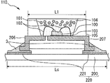
図16は、実施の形態に対する比較例として示す、LED素子110と基板220の接続構造の平面図である。図17は、図16のB−B線に沿ってLED素子110を切断した断面図である。LED素子110のケース105は実施の形態1と同様に横幅L1を有しているが、アノード電極206およびカソード電極207の先端部がパッケージの外側に突き出ている。このため、これらの電極を含めた横幅が、図16に示すとおり、L1を超える大きさLbとなっている。
FIG. 16 is a plan view of the connection structure between the
さらに、接続部材3がアノード電極206およびカソード電極207の先端部を覆うように広範囲に塗布されている。なお、接続部材3は、後述する実施の形態2でも述べるが、半田などの接続手段である。
Further, the connecting
その結果、半田等の接続部材3のフィレットが、LED素子10の外形のさらに外側の領域まで及んでしまう。これに応じて、基板220の基板電極221の外側端部の寸法Lcも、基板20の基板電極201よりも大きな幅となっている。その結果、この比較例では、実施の形態1に比して、実装面積が大きくなってしまうという問題がある。
As a result, the fillet of the connecting
図18は、実施の形態に対する比較例として示す、LED素子10と基板220の接続構造を示す図である。図19は、図18のC−C線に沿ってLED素子110および基板220を切断した断面図である。図18および図19に示す比較例では、実施の形態1と同じLED素子10であるため、アノード電極106およびカソード電極107を含めた寸法は実施の形態1と同じくL1である。しかし、基板電極221の外側端部の寸法Leが実施の形態1の場合に比して大きくなっており、接続部材3を基板電極221に合わせて広範囲に塗布しているので、実装面積が大きくなってしまうという問題がある。
FIG. 18 is a diagram illustrating a connection structure between the
これに対し、実施の形態1にかかる基板20においては、基板電極201の各部分が、先端部106cおよび107cとそれぞれ同じ大きさである。さらに、基板電極201の各部分が、先端部106c、107cと対向する領域にのみ形成されている。従って、実装面積を最小限にすることができる。
On the other hand, in the
なお、ここでは上記特許文献に記載の技術的課題についても、概略的に説明する。
特許文献1に記載の技術は、異なる複数の向きにLEDから光を出射させるため、異なる複数の向きに対応して、LEDを載置(実装)する複数の基板を用いて構成する必要があり、構造が複雑であるという問題があった。
Here, the technical problems described in the above-mentioned patent documents will also be schematically described.
Since the technique described in Patent Document 1 emits light from LEDs in a plurality of different directions, it is necessary to configure using a plurality of substrates on which LEDs are mounted (mounted) corresponding to the different directions. There was a problem that the structure was complicated.
特許文献2に記載の技術は、LED素子を載置(実装)する基板を、ガラス管の内面の離間した2箇所に架橋することを前提にしており、LED素子の外形寸法をはるかに超える短辺(幅)寸法を有する基板が必要となり、基板の材料費を増大させてしまうという問題があった。特許文献3および特許文献4に記載の技術も同様の課題を有していた。
The technique described in
また、特許文献2に記載の技術では、この特許文献2の図3等に図示されているとおり、LED素子がパッケージ外形からさらに外側に突き出た部分を備えている。これは、上記の図17および図19に記載の比較例と同種の構造であり、上記比較例と同様の問題点を有していた。
Further, in the technique described in
さらに、特許文献3には透光性の基板を用いると記載されているが、ガラス管内の中心軸付近にLED素子が配設される構造である。この場合、配光範囲(角度)は最大とならず、また、基板の両端部を保持するために設けられる凹部は配光特性を不連続とし、光学特性の面でも課題を有していた。
Further,
(実施の形態1の効果)
実施の形態1において、基板20の幅(短辺の長さ)を寸法W1として、LED素子10の発光面を、筒管4の筒方向の中心軸OからD1だけLED素子10の光出射方向と逆側に偏移させている。発光部7を筒管4の内面に近接して配設するので、発光部7が器具側への光を遮蔽する範囲が最小となり、照明ランプ1は最大の配光角度を得ることができる。しかも、基板20は透光性の基材200で形成されているので、さらなる広配光角の向上が達成される。
(Effect of Embodiment 1)
In the first embodiment, the width (short side length) of the
実施の形態1において、基板20の幅(短辺の長さ)寸法Wは、必要最低限の面積に応じたものである。基板20は最小面積となるので、軽量化と材料コストの低減に寄与する。透光性の基板材料を用いた場合であっても、コストアップを避けることができる。
In the first embodiment, the width (short side length) dimension W of the
また、基板20を小型化することによって、基板20は、複雑な構成を必要とすることなく簡素な方法で筒管4の内部空間に取付けが可能となるので、軽量化、材料コストの低減、および製造コストの低減、製造品質の安定化に寄与する。
Further, by reducing the size of the
[実施の形態1の変形例]
以下、図面を参照しつつ、実施の形態1の他の変形例を説明する。LEDパッケージのサイズが多少大きい場合や、LEDパッケージを長尺方法に並列に載置する場合などには、基板の幅(短辺の長さ)は、最小寸法以外のバリエーションから選択されてもよい。
[Modification of Embodiment 1]
Hereinafter, another modification of the first embodiment will be described with reference to the drawings. When the size of the LED package is somewhat large, or when the LED package is placed in parallel in the long method, the width of the substrate (the length of the short side) may be selected from variations other than the minimum dimension. .
図6は、本発明の実施の形態1の第1変形例にかかる照明ランプの主要構成と特徴を説明する断面図である。図7は、本発明の実施の形態1の第1変形例にかかる照明ランプの配光角を示す図である。 FIG. 6 is a cross-sectional view illustrating the main configuration and characteristics of an illumination lamp according to a first modification of the first embodiment of the present invention. FIG. 7 is a diagram showing a light distribution angle of the illumination lamp according to the first modification of the first embodiment of the present invention.
第1変形例では、幅W2を備える基板20aを用いている点が、実施の形態1とは異なっている。W2は、W1よりも大きい。基板20aが幅W2を備えることで、本変形例では、LED素子10の発光面は、筒管4の筒方向の中心軸OからD2だけ器具側に偏移して、筒管4の内面に近接して配設される。D2は、D1よりも小さい。
The first modification is different from the first embodiment in that a
図8は、本発明の実施の形態1の第2変形例にかかる照明ランプの主要構成と特徴を説明する断面図である。図9は、本発明の実施の形態1の第2変形例にかかる照明ランプの配光角を示す図である。 FIG. 8: is sectional drawing explaining the main structures and characteristics of the illumination lamp concerning the 2nd modification of Embodiment 1 of this invention. FIG. 9 is a diagram showing a light distribution angle of the illumination lamp according to the second modification of the first embodiment of the present invention.
第2変形例では、幅W3を備える基板20bを用いている点が、実施の形態1とは異なっている。W3は、W2よりも大きい。基板20bが幅W3を備えることで、本変形例では、LED素子10の発光面は、筒管4の筒方向の中心軸OからD3だけ器具側に偏移して、筒管4の内面に近接して配設される。D3は、D2よりも小さい。
The second modification is different from the first embodiment in that a
図10は、本発明の実施の形態1の第3変形例にかかる照明ランプの主要構成と特徴を説明する断面図である。図11は、本発明の実施の形態1の第3変形例にかかる照明ランプの配光角を示す図である。 FIG. 10: is sectional drawing explaining the main structures and the characteristics of the illumination lamp concerning the 3rd modification of Embodiment 1 of this invention. FIG. 11 is a diagram showing a light distribution angle of the illumination lamp according to the third modification of the first embodiment of the present invention.
第3変形例では、幅W4を備える基板20cを用いている点が、実施の形態1とは異なっている。W4は、W3よりも大きい。基板20cが幅W4を備えることで、本変形例では、LED素子10の発光面は、筒管4の筒方向の中心軸OからD4だけ器具側に偏移して、筒管4の内面に近接して配設される。D4は、D3よりも小さい。
The third modification is different from the first embodiment in that a
図15は、実施の形態1およびその第1〜3変形例が有する、比較例に対する優位性を説明するための表である。実施の形態1およびその第1〜3変形例が有する有利な効果について、比較例と対比しつつ説明する。 FIG. 15 is a table for explaining the advantages of the first embodiment and its first to third modifications over the comparative example. Advantageous effects of the first embodiment and its first to third modifications will be described in comparison with a comparative example.
図15の表は、筒管4の筒方向の中心軸Oから偏移させた距離D1〜D4と、基板20a〜20dそれぞれの幅W1〜W4とを備える場合の、配光角θ2(度)のシミュレーション結果をまとめたものである。図13および図14に示した比較例では、D=0.00〔mm〕、W=24.00〔mm〕である。この表に示すように、実施の形態1およびその変形例では、比較例と比べて、配光角θ2が飛躍的に大きくなっている。
The table of FIG. 15 shows the light distribution angle θ2 (degrees) when the distances D1 to D4 shifted from the central axis O of the
なお、実施の形態1では、パッケージ化されたLED素子10を、基板20に実装している。しかしながら、本発明はこれに限られるものではなく、LEDチップ100を直接に基板20に実装するいわゆるベアチップ実装技術を用いてもよい。その場合の実装方法は、フリップチップ実装であることが好ましく、超音波接合工法、圧接工法、溶接工法のいずれかを用いてもよい。
In the first embodiment, the packaged
LEDチップ100を基板20にベアチップ実装する場合には、LEDチップ100そのものが「LED素子本体」に相当する。そして、LEDチップ100の裏面に設けられるべき電極(具体的には、金属バンプ)が、「素子電極」に相当する。
When the
この変形例においてLEDチップ100のベアチップ実装を行う場合にも、LED素子本体(LEDチップ100)の裏面の面内において、素子電極(金属バンプ)および基板電極が収まっていることが好ましい。これにより、実装面積を極小化することができる。
Even in the case where the bare chip mounting of the
実施の形態1では、基板20をガラス等の透光性の基材200で形成したが、フィルム状(シート状)の基板であって透光性あるいは半透光性のものを使用してもよい。筒管4の内面に接するように、このフィルム状の基板を曲げて取り付けてもよい。
In the first embodiment, the
こうすることで、LED素子10の発光面を、筒管4の筒方向の中心軸Oから最大限、器具側に偏移させることができ、筒管4の内面に最大限近接して配設することができる。よって、一層の広配光角化が可能であり、また、軽量化も可能となる。
In this way, the light emitting surface of the
フィルム状の基板に対しても、LEDチップ100を直接に実装してもよい。また、基板20を非透光性の基材で形成してもよい。少なくとも中心軸Oからの偏移により得られる広配光角化の効果は得られるからである。
The
筒管4の素材は、ガラス素材の筒管と樹脂素材の筒管とを積層構造としたハイブリッド管でも良い。口金(実施の形態1ではアース口金5および給電口金6)のタイプは限定しない。嵌合部(実施の形態1ではアース口金5の第1嵌合部52および給電口金6の第2嵌合部62)の構造や口金と筒管との嵌合の方法は、図1に示した具体的構造に限定されるものではない。
The material of the
実施の形態2.
実施の形態2にかかる照明ランプ1は、LED素子10において接続部材3が用いられている点を除き、実施の形態1と同様の構成を備えている。従って、実施の形態2にかかる照明ランプ1も、実施の形態1と同様に、筒管4および発光部7を備える。
The illumination lamp 1 according to the second embodiment has the same configuration as that of the first embodiment except that the
図12は、本発明の実施の形態2にかかるLED素子と基板との接続を示す断面図である。以下、図12を参照して、LED素子10と基板20との接続(実施の形態1との相異部分)を説明する。実施の形態2にかかるフリップチップ実装方法では、接続部材3を用いて、基板電極(パッド)201とLED素子10が有するアノード電極106およびカソード電極107とを接続する。
FIG. 12: is sectional drawing which shows the connection of the LED
接続部材3としては、半田、導電ペースト、ACF(異方性導電フィルム)、ACP(異方性導電ペースト)、金属バンプ等を用いることができる。具体的な好ましいパッケージタイプとしては、実施の形態1と同様に、SOJ、BGA、LGA、LLCCを用いてもよい。
As the
実施の形態2では、接続部材3は、アノード電極106およびカソード電極107の先端部106c、107cにのみ設けられている。さらに、基板電極201が先端部106c、107cと同じ大きさであり、且つ接続部材3が先端部106c、107cと対向する領域をはみ出さないように形成されている。従って、実装面積を最小限にすることができる。
In the second embodiment, the
実施の形態2においても、実施の形態1と同様に、配光角度の最大化、基板20を最小面積とすることによる軽量化および材料コスト低減、基板20の小型化に伴う製造コスト低減、製造品質安定化といった効果を得ることができる。
Also in the second embodiment, similarly to the first embodiment, the light distribution angle is maximized, the weight is reduced by reducing the
1 照明ランプ(直管形LEDランプ)、10、110 LED素子、11 LED素子本体、100 LEDチップ、101 蛍光体、102 ワイヤ、103 接着部材、104 封止部材、105 ケース、106 アノード電極、107 カソード電極、106a、107a 平面部、106b、107b 側面部、106c、107c 先端部、20、20a、20b、20c、20d 基板、200 基材、201 基板電極、201a 外側端部、201b 外側端部、206 アノード電極、207 カソード電極、220 基板、221 基板電極、3 接続部材、4 筒管、40 第1端部、41 第2端部、5 アース口金、50 第1口金筐体、51 アース端子、52 第1嵌合部、6 給電口金、60 第2口金筐体、61 給電端子、62 第2嵌合部、7 発光部
DESCRIPTION OF SYMBOLS 1 Illumination lamp (straight tube type LED lamp) 10, 110 LED element, 11 LED element main body, 100 LED chip, 101 Phosphor, 102 Wire, 103 Adhesive member, 104 Sealing member, 105 Case, 106 Anode electrode, 107 Cathode electrode, 106a, 107a Plane portion, 106b, 107b Side surface portion, 106c, 107c Tip portion, 20, 20a, 20b, 20c, 20d Substrate, 200 base material, 201 substrate electrode, 201a outer end portion, 201b outer end portion, 206 Anode electrode, 207 Cathode electrode, 220 Substrate, 221 Substrate electrode, 3 Connection member, 4 Tube, 40 First end, 41 Second end, 5 Ground cap, 50 First cap housing, 51 Ground terminal, 52 1st fitting part, 6 Power supply base, 60 2nd base case, 61
Claims (6)
前記発光部を内部に収納し、前記発光部から出射される光を透過する筒管と、
を備え、
前記発光部は、
前記筒管の中心軸の側を向く表面に基板電極を備える基板と、
前記基板電極に実装された発光素子と、
を備え、
前記発光素子は、LEDチップを含む発光素子本体と、前記発光素子本体における前記基板電極と対向する裏面に設けられた素子電極と、を備えており、
前記発光素子は、前記LEDチップの平面視において、互いに直行する第一幅及び第二幅を備え、
前記第一幅の方向軸と平行な面で切断したときの断面視において、前記素子電極は、前記発光素子本体の前記裏面と重なる実装部と、前記実装部の外周端から前記発光素子本体の下側方向へ延び前記発光素子の側面を構成し前記発光素子の外部に露出された側面部と、前記側面部の下方端部から前記発光素子本体の下方領域の内側に伸び前記基板電極に重なる先端部と、を含むコの字の形状を有し、
前記LEDチップは、前記素子電極の前記実装部に実装され、
前記発光素子本体は、前記LEDチップを覆う封止樹脂を含み、
前記平面視において、前記素子電極および前記基板電極は、前記発光素子本体の前記裏面の面内に収まる大きさに設けられており、
前記平面視において、前記素子電極の外形の大きさと前記発光素子本体の前記裏面の外形の大きさとが同じであり、
前記基板は、前記筒管の内径よりも小さな幅を備え、前記中心軸から前記筒管の内面側に偏らせて配置されたことを特徴とする照明ランプ。 A light emitting unit;
A cylindrical tube that houses the light emitting unit therein and transmits light emitted from the light emitting unit;
With
The light emitting portion,
A substrate Ru with a board electrode on the surface facing the side of the center axis of the cylinder tube,
A luminescent element mounted on the substrate electrode,
With
The light-emitting element includes a light-emitting element body including an LED chip, and an element electrode provided on the back surface of the light-emitting element body facing the substrate electrode.
The light emitting element has a first width and a second width that are orthogonal to each other in a plan view of the LED chip,
In a cross-sectional view when cut along a plane parallel to the direction axis of the first width, the element electrode includes a mounting part that overlaps the back surface of the light emitting element body, and an outer peripheral end of the mounting part from the outer peripheral end of the light emitting element body. A side surface portion that extends downward and constitutes a side surface of the light emitting element and is exposed to the outside of the light emitting element, and extends from a lower end portion of the side surface portion to an inner side of a lower region of the light emitting element body and overlaps the substrate electrode And a U-shaped shape including the tip,
The LED chip is mounted on the mounting portion of the element electrode,
The light emitting device body includes a Futomeju fat covering the front Symbol LED chip,
In the plan view, the element electrode and the substrate electrode are provided in a size that fits within the surface of the back surface of the light emitting element body,
In the plan view, and are the same size of the rear surface of the outer shape size and the light-emitting element body of the outer shape of the element electrodes,
The illumination lamp according to claim 1, wherein the substrate has a width smaller than an inner diameter of the cylindrical tube, and is arranged so as to be biased toward the inner surface side of the cylindrical tube from the central axis.
前記フィルム状基板が、前記筒管の内面に接するように曲げられて配置されたことを特徴とする請求項1に記載の照明ランプ。 The substrate is a film substrate,
The illumination lamp according to claim 1, wherein the film-like substrate is arranged so as to be in contact with the inner surface of the cylindrical tube.
前記接続部材は、前記基板電極と前記素子電極とが対向する領域をはみ出さないように設けられたことを特徴とする請求項1または2に記載の照明ランプ。 The substrate electrode and the element electrode are connected via a connection member,
The illumination lamp according to claim 1, wherein the connection member is provided so as not to protrude from a region where the substrate electrode and the element electrode face each other.
前記照明ランプと接続する点灯装置と、
を備えることを特徴とする照明装置。 The illumination lamp according to any one of claims 1 to 5,
A lighting device connected to the illumination lamp;
A lighting device comprising:
Priority Applications (1)
| Application Number | Priority Date | Filing Date | Title |
|---|---|---|---|
| JP2013082418A JP6286857B2 (en) | 2013-04-10 | 2013-04-10 | Lighting lamp and lighting device |
Applications Claiming Priority (1)
| Application Number | Priority Date | Filing Date | Title |
|---|---|---|---|
| JP2013082418A JP6286857B2 (en) | 2013-04-10 | 2013-04-10 | Lighting lamp and lighting device |
Related Child Applications (1)
| Application Number | Title | Priority Date | Filing Date |
|---|---|---|---|
| JP2018018310A Division JP6540837B2 (en) | 2018-02-05 | 2018-02-05 | Lighting device |
Publications (2)
| Publication Number | Publication Date |
|---|---|
| JP2014207057A JP2014207057A (en) | 2014-10-30 |
| JP6286857B2 true JP6286857B2 (en) | 2018-03-07 |
Family
ID=52120482
Family Applications (1)
| Application Number | Title | Priority Date | Filing Date |
|---|---|---|---|
| JP2013082418A Active JP6286857B2 (en) | 2013-04-10 | 2013-04-10 | Lighting lamp and lighting device |
Country Status (1)
| Country | Link |
|---|---|
| JP (1) | JP6286857B2 (en) |
Families Citing this family (2)
| Publication number | Priority date | Publication date | Assignee | Title |
|---|---|---|---|---|
| JP6699987B2 (en) * | 2015-02-23 | 2020-05-27 | 株式会社アルバジャパン | LED lamp and heat dissipation method of LED lamp |
| JP2016170981A (en) * | 2015-03-12 | 2016-09-23 | パナソニックIpマネジメント株式会社 | Luminaire |
Family Cites Families (9)
| Publication number | Priority date | Publication date | Assignee | Title |
|---|---|---|---|---|
| JP3658426B2 (en) * | 1995-01-23 | 2005-06-08 | 株式会社日立製作所 | Optical semiconductor device |
| JP4561056B2 (en) * | 2003-07-17 | 2010-10-13 | ソニー株式会社 | Manufacturing method of light source device |
| JP4789673B2 (en) * | 2005-10-27 | 2011-10-12 | 京セラ株式会社 | Light emitting element storage package, and light source and light emitting device using the same |
| JP2009033061A (en) * | 2007-07-30 | 2009-02-12 | Sanyo Electric Co Ltd | Light-emitting device and imaging device |
| JP2009289724A (en) * | 2008-05-28 | 2009-12-10 | Sigma Denki Kogyo Kk | Method for manufacturing cylindrical decorative illumination body and method of controlling light emitting direction of cylindrical decorative illumination body |
| TW201003991A (en) * | 2008-07-03 | 2010-01-16 | jia-han Xie | Package structure of LED and light bar using the same |
| JP5585013B2 (en) * | 2009-07-14 | 2014-09-10 | 日亜化学工業株式会社 | Light emitting device |
| JP5834224B2 (en) * | 2009-12-28 | 2015-12-16 | パナソニックIpマネジメント株式会社 | LED lamp |
| JP5651464B2 (en) * | 2010-12-28 | 2015-01-14 | パナソニックIpマネジメント株式会社 | Lamp and lighting device |
-
2013
- 2013-04-10 JP JP2013082418A patent/JP6286857B2/en active Active
Also Published As
| Publication number | Publication date |
|---|---|
| JP2014207057A (en) | 2014-10-30 |
Similar Documents
| Publication | Publication Date | Title |
|---|---|---|
| US8405118B2 (en) | Multichip package structure using a constant voltage power supply | |
| CN103180661B (en) | Lamp and lighting device | |
| US9078312B2 (en) | Multichip package structure for directly electrically connecting to an AC power source | |
| TWI408794B (en) | Light-mixing multichip package structure | |
| JP5291268B1 (en) | LIGHT EMITTING MODULE AND LIGHTING LIGHT SOURCE AND LIGHTING DEVICE USING THE SAME | |
| US20130249381A1 (en) | Light bulb shaped lamp and lighting apparatus | |
| JP4866975B2 (en) | LED lamp and lighting fixture | |
| US9634211B2 (en) | Light-emitting module | |
| JP6056213B2 (en) | Light emitting module and lighting device | |
| JP2011192703A (en) | Light emitting device, and illumination apparatus | |
| JP5627801B2 (en) | Light emitting device, light bulb shaped lamp and lighting device | |
| US8764231B2 (en) | Light-emitting diode light source | |
| JP6286857B2 (en) | Lighting lamp and lighting device | |
| CN210866193U (en) | COB substrate | |
| JP6095440B2 (en) | LIGHTING LAMP, LIGHTING DEVICE, AND LIGHTING LAMP MANUFACTURING METHOD | |
| JP6540837B2 (en) | Lighting device | |
| JP2013115005A (en) | Lighting apparatus | |
| CN214198200U (en) | Flip-chip COB module lamp strip | |
| JP5179311B2 (en) | Light emitting device | |
| TWM322064U (en) | Surface mount light emitting diode package | |
| TW201538888A (en) | LED lighting device and LED lamp | |
| JP4442557B2 (en) | LED unit | |
| TWI466332B (en) | Led package structure | |
| KR101694178B1 (en) | Light Emitting Device | |
| KR20120067542A (en) | Light emitting module and backlight unit using the same |
Legal Events
| Date | Code | Title | Description |
|---|---|---|---|
| A621 | Written request for application examination |
Free format text: JAPANESE INTERMEDIATE CODE: A621 Effective date: 20160317 |
|
| A977 | Report on retrieval |
Free format text: JAPANESE INTERMEDIATE CODE: A971007 Effective date: 20161221 |
|
| A131 | Notification of reasons for refusal |
Free format text: JAPANESE INTERMEDIATE CODE: A131 Effective date: 20170110 |
|
| A521 | Request for written amendment filed |
Free format text: JAPANESE INTERMEDIATE CODE: A523 Effective date: 20170202 |
|
| A131 | Notification of reasons for refusal |
Free format text: JAPANESE INTERMEDIATE CODE: A131 Effective date: 20170808 |
|
| A521 | Request for written amendment filed |
Free format text: JAPANESE INTERMEDIATE CODE: A523 Effective date: 20170908 |
|
| TRDD | Decision of grant or rejection written | ||
| A01 | Written decision to grant a patent or to grant a registration (utility model) |
Free format text: JAPANESE INTERMEDIATE CODE: A01 Effective date: 20180109 |
|
| A61 | First payment of annual fees (during grant procedure) |
Free format text: JAPANESE INTERMEDIATE CODE: A61 Effective date: 20180122 |
|
| R150 | Certificate of patent or registration of utility model |
Ref document number: 6286857 Country of ref document: JP Free format text: JAPANESE INTERMEDIATE CODE: R150 |
|
| R250 | Receipt of annual fees |
Free format text: JAPANESE INTERMEDIATE CODE: R250 |
|
| R250 | Receipt of annual fees |
Free format text: JAPANESE INTERMEDIATE CODE: R250 |
|
| R250 | Receipt of annual fees |
Free format text: JAPANESE INTERMEDIATE CODE: R250 |
|
| R250 | Receipt of annual fees |
Free format text: JAPANESE INTERMEDIATE CODE: R250 |