JP6263628B2 - Frame-based package for flip chip LEDs - Google Patents
Frame-based package for flip chip LEDs Download PDFInfo
- Publication number
- JP6263628B2 JP6263628B2 JP2016542405A JP2016542405A JP6263628B2 JP 6263628 B2 JP6263628 B2 JP 6263628B2 JP 2016542405 A JP2016542405 A JP 2016542405A JP 2016542405 A JP2016542405 A JP 2016542405A JP 6263628 B2 JP6263628 B2 JP 6263628B2
- Authority
- JP
- Japan
- Prior art keywords
- light emitting
- substrate
- frame
- cap
- hole
- Prior art date
- Legal status (The legal status is an assumption and is not a legal conclusion. Google has not performed a legal analysis and makes no representation as to the accuracy of the status listed.)
- Active
Links
- 239000000758 substrate Substances 0.000 claims description 38
- 239000000463 material Substances 0.000 claims description 29
- 238000000034 method Methods 0.000 claims description 26
- 230000003287 optical effect Effects 0.000 claims description 16
- 239000004065 semiconductor Substances 0.000 claims description 11
- 238000006243 chemical reaction Methods 0.000 claims description 8
- 229910052594 sapphire Inorganic materials 0.000 claims description 6
- 239000010980 sapphire Substances 0.000 claims description 6
- 239000002654 heat shrinkable material Substances 0.000 claims description 2
- 238000004513 sizing Methods 0.000 claims 1
- 230000008569 process Effects 0.000 description 9
- 239000004020 conductor Substances 0.000 description 6
- 239000008393 encapsulating agent Substances 0.000 description 5
- 239000007788 liquid Substances 0.000 description 5
- 239000000853 adhesive Substances 0.000 description 4
- 230000001070 adhesive effect Effects 0.000 description 4
- 239000011248 coating agent Substances 0.000 description 3
- 238000000576 coating method Methods 0.000 description 3
- 238000000605 extraction Methods 0.000 description 3
- 230000007246 mechanism Effects 0.000 description 3
- OAICVXFJPJFONN-UHFFFAOYSA-N Phosphorus Chemical compound [P] OAICVXFJPJFONN-UHFFFAOYSA-N 0.000 description 2
- 230000008901 benefit Effects 0.000 description 2
- 238000005520 cutting process Methods 0.000 description 2
- 238000003780 insertion Methods 0.000 description 2
- 230000037431 insertion Effects 0.000 description 2
- 238000003698 laser cutting Methods 0.000 description 2
- 229920001296 polysiloxane Polymers 0.000 description 2
- 239000011253 protective coating Substances 0.000 description 2
- 235000001674 Agaricus brunnescens Nutrition 0.000 description 1
- JMASRVWKEDWRBT-UHFFFAOYSA-N Gallium nitride Chemical compound [Ga]#N JMASRVWKEDWRBT-UHFFFAOYSA-N 0.000 description 1
- BQCADISMDOOEFD-UHFFFAOYSA-N Silver Chemical compound [Ag] BQCADISMDOOEFD-UHFFFAOYSA-N 0.000 description 1
- 229910010413 TiO 2 Inorganic materials 0.000 description 1
- 238000005452 bending Methods 0.000 description 1
- 230000009286 beneficial effect Effects 0.000 description 1
- 230000002860 competitive effect Effects 0.000 description 1
- 238000010276 construction Methods 0.000 description 1
- 230000008878 coupling Effects 0.000 description 1
- 238000010168 coupling process Methods 0.000 description 1
- 238000005859 coupling reaction Methods 0.000 description 1
- 230000001419 dependent effect Effects 0.000 description 1
- 230000004069 differentiation Effects 0.000 description 1
- 238000009826 distribution Methods 0.000 description 1
- 238000005538 encapsulation Methods 0.000 description 1
- 239000012467 final product Substances 0.000 description 1
- 239000011521 glass Substances 0.000 description 1
- 239000011344 liquid material Substances 0.000 description 1
- 238000004519 manufacturing process Methods 0.000 description 1
- 238000004806 packaging method and process Methods 0.000 description 1
- 238000012858 packaging process Methods 0.000 description 1
- 239000000047 product Substances 0.000 description 1
- 239000000565 sealant Substances 0.000 description 1
- 229910052709 silver Inorganic materials 0.000 description 1
- 239000004332 silver Substances 0.000 description 1
- 239000007921 spray Substances 0.000 description 1
- 239000010409 thin film Substances 0.000 description 1
Images


Classifications
-
- H—ELECTRICITY
- H01—ELECTRIC ELEMENTS
- H01L—SEMICONDUCTOR DEVICES NOT COVERED BY CLASS H10
- H01L33/00—Semiconductor devices with at least one potential-jump barrier or surface barrier specially adapted for light emission; Processes or apparatus specially adapted for the manufacture or treatment thereof or of parts thereof; Details thereof
- H01L33/48—Semiconductor devices with at least one potential-jump barrier or surface barrier specially adapted for light emission; Processes or apparatus specially adapted for the manufacture or treatment thereof or of parts thereof; Details thereof characterised by the semiconductor body packages
- H01L33/58—Optical field-shaping elements
- H01L33/60—Reflective elements
-
- H—ELECTRICITY
- H01—ELECTRIC ELEMENTS
- H01L—SEMICONDUCTOR DEVICES NOT COVERED BY CLASS H10
- H01L33/00—Semiconductor devices with at least one potential-jump barrier or surface barrier specially adapted for light emission; Processes or apparatus specially adapted for the manufacture or treatment thereof or of parts thereof; Details thereof
- H01L33/48—Semiconductor devices with at least one potential-jump barrier or surface barrier specially adapted for light emission; Processes or apparatus specially adapted for the manufacture or treatment thereof or of parts thereof; Details thereof characterised by the semiconductor body packages
- H01L33/483—Containers
-
- H—ELECTRICITY
- H01—ELECTRIC ELEMENTS
- H01L—SEMICONDUCTOR DEVICES NOT COVERED BY CLASS H10
- H01L25/00—Assemblies consisting of a plurality of individual semiconductor or other solid state devices ; Multistep manufacturing processes thereof
- H01L25/03—Assemblies consisting of a plurality of individual semiconductor or other solid state devices ; Multistep manufacturing processes thereof all the devices being of a type provided for in the same subgroup of groups H01L27/00 - H01L33/00, or in a single subclass of H10K, H10N, e.g. assemblies of rectifier diodes
- H01L25/04—Assemblies consisting of a plurality of individual semiconductor or other solid state devices ; Multistep manufacturing processes thereof all the devices being of a type provided for in the same subgroup of groups H01L27/00 - H01L33/00, or in a single subclass of H10K, H10N, e.g. assemblies of rectifier diodes the devices not having separate containers
- H01L25/075—Assemblies consisting of a plurality of individual semiconductor or other solid state devices ; Multistep manufacturing processes thereof all the devices being of a type provided for in the same subgroup of groups H01L27/00 - H01L33/00, or in a single subclass of H10K, H10N, e.g. assemblies of rectifier diodes the devices not having separate containers the devices being of a type provided for in group H01L33/00
- H01L25/0753—Assemblies consisting of a plurality of individual semiconductor or other solid state devices ; Multistep manufacturing processes thereof all the devices being of a type provided for in the same subgroup of groups H01L27/00 - H01L33/00, or in a single subclass of H10K, H10N, e.g. assemblies of rectifier diodes the devices not having separate containers the devices being of a type provided for in group H01L33/00 the devices being arranged next to each other
-
- H—ELECTRICITY
- H01—ELECTRIC ELEMENTS
- H01L—SEMICONDUCTOR DEVICES NOT COVERED BY CLASS H10
- H01L33/00—Semiconductor devices with at least one potential-jump barrier or surface barrier specially adapted for light emission; Processes or apparatus specially adapted for the manufacture or treatment thereof or of parts thereof; Details thereof
- H01L33/005—Processes
- H01L33/0062—Processes for devices with an active region comprising only III-V compounds
- H01L33/0075—Processes for devices with an active region comprising only III-V compounds comprising nitride compounds
-
- H—ELECTRICITY
- H01—ELECTRIC ELEMENTS
- H01L—SEMICONDUCTOR DEVICES NOT COVERED BY CLASS H10
- H01L33/00—Semiconductor devices with at least one potential-jump barrier or surface barrier specially adapted for light emission; Processes or apparatus specially adapted for the manufacture or treatment thereof or of parts thereof; Details thereof
- H01L33/48—Semiconductor devices with at least one potential-jump barrier or surface barrier specially adapted for light emission; Processes or apparatus specially adapted for the manufacture or treatment thereof or of parts thereof; Details thereof characterised by the semiconductor body packages
- H01L33/483—Containers
- H01L33/486—Containers adapted for surface mounting
-
- H—ELECTRICITY
- H01—ELECTRIC ELEMENTS
- H01L—SEMICONDUCTOR DEVICES NOT COVERED BY CLASS H10
- H01L33/00—Semiconductor devices with at least one potential-jump barrier or surface barrier specially adapted for light emission; Processes or apparatus specially adapted for the manufacture or treatment thereof or of parts thereof; Details thereof
- H01L33/48—Semiconductor devices with at least one potential-jump barrier or surface barrier specially adapted for light emission; Processes or apparatus specially adapted for the manufacture or treatment thereof or of parts thereof; Details thereof characterised by the semiconductor body packages
- H01L33/50—Wavelength conversion elements
- H01L33/501—Wavelength conversion elements characterised by the materials, e.g. binder
- H01L33/502—Wavelength conversion materials
-
- H—ELECTRICITY
- H01—ELECTRIC ELEMENTS
- H01L—SEMICONDUCTOR DEVICES NOT COVERED BY CLASS H10
- H01L2924/00—Indexing scheme for arrangements or methods for connecting or disconnecting semiconductor or solid-state bodies as covered by H01L24/00
- H01L2924/10—Details of semiconductor or other solid state devices to be connected
- H01L2924/11—Device type
- H01L2924/12—Passive devices, e.g. 2 terminal devices
- H01L2924/1204—Optical Diode
- H01L2924/12041—LED
-
- H—ELECTRICITY
- H01—ELECTRIC ELEMENTS
- H01L—SEMICONDUCTOR DEVICES NOT COVERED BY CLASS H10
- H01L2933/00—Details relating to devices covered by the group H01L33/00 but not provided for in its subgroups
- H01L2933/0008—Processes
- H01L2933/0033—Processes relating to semiconductor body packages
-
- H—ELECTRICITY
- H01—ELECTRIC ELEMENTS
- H01L—SEMICONDUCTOR DEVICES NOT COVERED BY CLASS H10
- H01L2933/00—Details relating to devices covered by the group H01L33/00 but not provided for in its subgroups
- H01L2933/0008—Processes
- H01L2933/0033—Processes relating to semiconductor body packages
- H01L2933/0041—Processes relating to semiconductor body packages relating to wavelength conversion elements
-
- H—ELECTRICITY
- H01—ELECTRIC ELEMENTS
- H01L—SEMICONDUCTOR DEVICES NOT COVERED BY CLASS H10
- H01L2933/00—Details relating to devices covered by the group H01L33/00 but not provided for in its subgroups
- H01L2933/0008—Processes
- H01L2933/0033—Processes relating to semiconductor body packages
- H01L2933/0058—Processes relating to semiconductor body packages relating to optical field-shaping elements
-
- H—ELECTRICITY
- H01—ELECTRIC ELEMENTS
- H01L—SEMICONDUCTOR DEVICES NOT COVERED BY CLASS H10
- H01L33/00—Semiconductor devices with at least one potential-jump barrier or surface barrier specially adapted for light emission; Processes or apparatus specially adapted for the manufacture or treatment thereof or of parts thereof; Details thereof
- H01L33/005—Processes
- H01L33/0095—Post-treatment of devices, e.g. annealing, recrystallisation or short-circuit elimination
-
- H—ELECTRICITY
- H01—ELECTRIC ELEMENTS
- H01L—SEMICONDUCTOR DEVICES NOT COVERED BY CLASS H10
- H01L33/00—Semiconductor devices with at least one potential-jump barrier or surface barrier specially adapted for light emission; Processes or apparatus specially adapted for the manufacture or treatment thereof or of parts thereof; Details thereof
- H01L33/48—Semiconductor devices with at least one potential-jump barrier or surface barrier specially adapted for light emission; Processes or apparatus specially adapted for the manufacture or treatment thereof or of parts thereof; Details thereof characterised by the semiconductor body packages
- H01L33/50—Wavelength conversion elements
-
- H—ELECTRICITY
- H01—ELECTRIC ELEMENTS
- H01L—SEMICONDUCTOR DEVICES NOT COVERED BY CLASS H10
- H01L33/00—Semiconductor devices with at least one potential-jump barrier or surface barrier specially adapted for light emission; Processes or apparatus specially adapted for the manufacture or treatment thereof or of parts thereof; Details thereof
- H01L33/48—Semiconductor devices with at least one potential-jump barrier or surface barrier specially adapted for light emission; Processes or apparatus specially adapted for the manufacture or treatment thereof or of parts thereof; Details thereof characterised by the semiconductor body packages
- H01L33/58—Optical field-shaping elements
-
- H—ELECTRICITY
- H01—ELECTRIC ELEMENTS
- H01L—SEMICONDUCTOR DEVICES NOT COVERED BY CLASS H10
- H01L33/00—Semiconductor devices with at least one potential-jump barrier or surface barrier specially adapted for light emission; Processes or apparatus specially adapted for the manufacture or treatment thereof or of parts thereof; Details thereof
- H01L33/48—Semiconductor devices with at least one potential-jump barrier or surface barrier specially adapted for light emission; Processes or apparatus specially adapted for the manufacture or treatment thereof or of parts thereof; Details thereof characterised by the semiconductor body packages
- H01L33/62—Arrangements for conducting electric current to or from the semiconductor body, e.g. lead-frames, wire-bonds or solder balls
Description
本発明は、発光デバイスの分野に関し、特に、デバイスの外縁周りに反射エンクロージャを提供するフレームに関する。 The present invention relates to the field of light emitting devices, and more particularly to a frame that provides a reflective enclosure around the outer edge of the device.
ますます拡大する半導体発光デバイスの使用が、これらのデバイスの高度に競争的な市場を作り出している。このような市場においては、数ある供給元の中での製品の差異化をもたらすのに性能と価格が重要であることが多い。従って、共通の目的は、発光デバイスから均等あるいは更に良好な性能を提供しながら、製造のコストを低減することである。 Increasing use of semiconductor light emitting devices has created a highly competitive market for these devices. In such a market, performance and price are often important in bringing product differentiation among a number of suppliers. Accordingly, a common objective is to reduce manufacturing costs while providing equal or better performance from light emitting devices.
発光素子の比較的安価なパッケージングを提供する1つの技術は、発光素子への外部接続を容易にするリードフレームコンタクトを備えたフレーム内に発光素子を配置することである。LEDリードフレームは一般的に、LEDへの外部接続を提供するように形状を整えられる一対の導電体を有する。リードフレームの周りに支持フレームが成形されて、LEDをマウントするための支持フレーム内の導電面と、フレーム化されたLEDを印刷回路基板又はその他の固定具にマウントするための支持フレームの外の導電面と、をリードフレームの導電体が提供するようにされ得る。 One technique for providing relatively inexpensive packaging of light emitting elements is to place the light emitting elements in a frame with lead frame contacts that facilitate external connection to the light emitting elements. An LED lead frame generally has a pair of conductors that are shaped to provide an external connection to the LED. A support frame is molded around the lead frame to provide a conductive surface within the support frame for mounting the LED and an exterior of the support frame for mounting the framed LED to a printed circuit board or other fixture. The conductor of the lead frame may be provided with a conductive surface.
ここに援用する特許文献1(USPA2010/0207140,“COMPACT MOLDED LED MODULE”,2010年8月19日発行,Serge L.Rudaz,Serge Bierhuizen,及びAshim S.Haque)は、図7A−7Bに例示されるように各支持フレームの中で発光デバイスがリードフレームコンタクトに接合された支持フレームのアレイを開示している。 Patent Document 1 (USPA2010 / 0207140, “COMPACT MOLDED LED MODULE”, issued on August 19, 2010, Serge L. Rudaz, Serge Bierhuizen, and Ashim S. Haque) incorporated herein is exemplified in FIGS. 7A-7B. An array of support frames is disclosed in which a light emitting device is joined to a lead frame contact in each support frame.
図7Aは、成形されたフレームアレイ40の中の2つのリードフレーム16を示している。各リードフレーム16は、導電体12及び14を含んでいる。この例においては、各リードフレーム16の周りにタブ10が形成されるとともに、リードフレーム16の導電体12及び14が、フレーム素子40を貫いて延在するように整形されて、タブ10内の、発光デバイスをマウントするためのコンタクト12a、14aと、発光デバイスを備えたタブ10のその後の印刷回路基板又はその他の固定具の上へのマウントのためのコンタクト12b、14bとを提供している。2つのみのリードフレーム16及びタブ10が図示されているが、成形されたフレームアレイ40は、何百ものリードフレーム16及びタブ10を含み得る。
FIG. 7A shows two
図7Bは、2つの発光モジュール38を示している。この実施形態例においては、最小限の固有の構造的支持を持つ薄膜デバイスとし得るものである発光デバイス20が、発光デバイス20に必要な構造的支持を提供するものであるサブマウント30上に置かれている。例えばESD保護デバイス26などのその他のデバイスも、サブマウント上に置かれ得る。サブマウント30上に保護コーティング28が設けられ得る。サブマウント30を貫く導電体24が、発光デバイス20をリードフレーム16のコンタクト12及び14に結合する。
FIG. 7B shows two
その後、タブ10が封止材で充填され得る。オプションとして、封止材、又は保護コーティング28、又は発光デバイス20は、放たれた光の一部又は全てを吸収して異なる波長の光を放出する例えば蛍光体などの波長変換材料を含んでいてもよい。タブ10の内壁15は、タブ10の外方へと光を向け直すために反射性とし得る。
Thereafter, the
完成後、ライン36に沿ってスライスすることによって、フレームアレイ40によって形成された個々の発光モジュール38が個片化される。個別にされた発光モジュール38は、発光モジュール38のピックアンドプレースを容易にする側面35を含むが、光生成素子20よりもかなり多くの体積を消費するとともに、光生成素子20の表面積と比較して大幅に大きいフットプリントを導入する。この相当な体積及びフットプリントの‘オーバーヘッド’は、例えばスマートフォン及びそれに類するものなどのポータブル装置用の例えばフラッシュ又は照明要素などの用途において、このような発光モジュールの使用を制限してしまう。
After completion, the individual
発光モジュールのハンドリングを容易にする側面と、発光面とは反対側のコンタクトとを有する発光モジュールを提供するための、より複雑でないプロセスを提供することが有利である。また、体積及びフットプリントのオーバーヘッドが最小限であるような発光モジュールを提供することも有利である。 It would be advantageous to provide a less complex process for providing a light emitting module having a side that facilitates handling of the light emitting module and a contact opposite the light emitting surface. It would also be advantageous to provide a light emitting module that has minimal volume and footprint overhead.
これらの関心事のうちの1つ以上を、より良く解決するため、本発明の一実施形態において、実質的に自己支持形のフリップチップ発光デバイスの外縁を取り囲むように中空フレームが構成される。当該フレームはまた、発光デバイスの発光面の上方に波長変換素子を収容するような形状にされ得る。中空フレームを通じて露出されるものである発光デバイスの下面が、発光モジュールを印刷回路基板又はその他の固定具に表面実装するための、発光素子に結合されたコンタクトパッドを含む。フリップチップ発光デバイスは、発光素子が上に成長されたパターンドサファイア基板(PSS)を含むことができ、パターン加工された表面が、このパターンドサファイア成長基板を通じての、発光素子からの高められた光取り出しをもたらす。 In order to better resolve one or more of these concerns, in one embodiment of the present invention, a hollow frame is configured to surround the outer edge of the substantially self-supporting flip chip light emitting device. The frame can also be shaped to accommodate the wavelength converting element above the light emitting surface of the light emitting device. The lower surface of the light emitting device that is exposed through the hollow frame includes contact pads coupled to the light emitting elements for surface mounting the light emitting module to a printed circuit board or other fixture. The flip-chip light emitting device can include a patterned sapphire substrate (PSS) on which the light emitting element is grown, and the patterned surface is enhanced from the light emitting element through the patterned sapphire growth substrate. Provides light extraction.
以下の図を含む添付図面を参照して、例として、本発明を更に詳細に説明する。
以下の説明においては、限定ではなく説明の目的で、本発明の概念の完全なる理解を提供するために、例えば特定のアーキテクチャ、インタフェース、技術などの具体的詳細事項を説明する。しかしながら、当業者に明らかなように、本発明は、これらの具体的詳細事項からは逸脱した他の実施形態でも実施され得るものである。同様に、本明細書の文章は、図面に示される実施形態例に向けられたものであり、請求項に係る発明に、請求項に明示的に含められた限定以外の限定を加えるものではない。単純化及び明瞭化の目的のため、不要な詳細事項で本発明の説明を不明瞭にしないよう、周知のデバイス、回路及び方法についての詳細な説明は省略することとする。 In the following description, for purposes of explanation and not limitation, specific details are set forth, such as specific architectures, interfaces, techniques, etc., in order to provide a thorough understanding of the concepts of the present invention. However, it will be apparent to those skilled in the art that the present invention may be practiced in other embodiments that depart from these specific details. Similarly, the text of this specification is directed to the exemplary embodiments shown in the drawings and does not impose limitations on the claimed invention other than those explicitly included in a claim. . For the purpose of simplicity and clarity, detailed descriptions of well-known devices, circuits, and methods are omitted so as not to obscure the description of the present invention with unnecessary detail.
厚くて自己支持形の発光デバイスは現在一般的に入手可能である。図8A−8Cは、幾つかの自己支持形の発光デバイス100の一例を示している。図8Aは、複数の発光デバイス100を作り出すように上に半導体層が形成/成長された基板110を示している。基板110は一般的にサファイア又はガラスであり、各デバイス100の発光素子120は一般的に、n型半導体層とp型半導体層との間に挟まれた活性領域を含む。パッド130がn層及びp層へのコンタクトを提供し、これらの層の間に電流が流れるときに活性領域から光が発せられるようにされる。発光素子120を形成する半導体として、一般的に、n型及びp型の半導体を提供するようにドープされた窒化ガリウム(GaN)が使用される。
Thick and self-supporting light emitting devices are now generally available. 8A-8C show examples of several self-supporting
単一の発光チップ100を供するため、基板110がスライス/ダイシングされ得る(図8A中の破線)。動作時、個々の発光チップは典型的に、コンタクトパッド130を図8Cに示すチップ100の名目上の‘底面’として、図8Bに示すように‘フリップチップ’構成の向きにされる。光は、主として発光素子120の‘頂’面125から基板110内に放たれ、その後、基板110の頂面115及び側面116から放出される。また、一部の光が発光素子120の側面126から放出される。
To provide a single
発光素子120から基板110への光取り出し効率を高めるため、基板110と発光素子120との界面が、該界面での全反射(TIR)の可能性を低減するように‘粗面化’され得る。一般に、基板110は、発光素子120が上に成長されるパターンドサファイア基板(Patterned Sapphire Substrate;PSS)であり、サファイア基板上のパターンが、上述の、基板110と発光素子120との間の‘粗面化’された界面を作り出す。
In order to increase the light extraction efficiency from the
発光デバイス100は実質的に自己支持形であるが、例えば印刷回路基板及びその他の固定具などのアセンブリなどの最終製品のアセンブリ中に様々なプロセスを経るので、発光デバイス100は一般的に、その後のハンドリングに耐えるように‘パッケージング’され得る。図7A−7Bの例においてのように、チップ100は、発光チップ100の各々への外部接続を可能にするリードフレーム内の導電体にパッド130をはんだ付けして、リードフレームのアレイ又はストリップの上に配置され得る。リードフレームのアレイは、発光チップの各々又は発光チップの組(セット)を封入するように処理され、そして、個々の封止(‘パッケージング’)された発光デバイスを提供するように個片化される。
Although the
封止は複数の目的を果たし、封止材は、発光チップを環境から保護するとともに、1つ以上の特定の光学機能を提供するように形成され得る。例えば、封止材は、発光チップ100から放たれた光の一部又は全てを異なる波長の光へと変換する例えば蛍光体などの波長変換材料を含み得る。封止材はまた、所望の光出力パターンを提供するレンズを形成するように形状を定められ得る。オプションとして、封止材は、例えば図7Bの発光モジュール38のタブ10などの反射壁によって形成されるウェル(井戸)の中に配置され得る。
Encapsulation serves multiple purposes, and the encapsulant can be formed to protect the light emitting chip from the environment and to provide one or more specific optical functions. For example, the encapsulant may include a wavelength conversion material such as a phosphor that converts part or all of the light emitted from the
図1A−1Fは、リードフレームの必要性を排除するとともに体積及びフットプリントのオーバーヘッドを最小限にするパッケージングプロセスを例示している。 1A-1F illustrate a packaging process that eliminates the need for lead frames and minimizes volume and footprint overhead.
図1Aは、その中に発光チップが配置され得る中空フレーム210の一例を示している。オプションとして、フレーム210の内壁215は、例えば銀(Ag)又はその他の反射材料のコーティングを用いて、反射性であり得る。フレーム210の開口の形状及び大きさは、図1Bに示すような発光チップ100の形状及び大きさに一致し得る。好ましくは、発光チップ100は、動作するチップ100のみがパッケージングされるよう、事前に試験される。
FIG. 1A shows an example of a
図1A−1Fは単一のフレーム210を示しているが、複数のフレーム210の同時アセンブリ及びテストを可能にするように、例えば図4に例示するようなフレーム210のアレイ400が提供され得る。
1A-1F show a
アセンブリ前に、アレイ400は、各フレーム210の内側の壁215上に反射材料を塗布するように処理され得る。パッケージングされたデバイスの意図した用途に応じて、アレイ400の全体が反射材料でスプレイコーティングされてもよく、あるいは、内壁に反射材料が塗布される間、フレーム210の上面がマスクされてもよい。反射コーティングを設けることには、アレイ400を反射材料のたる内に浸漬することを含め、その他の技術が使用されてもよい。一部の実施形態において、別個の反射コーティングを塗布する必要性を排除するよう、フレーム210の材料が生来的に反射性であってもよい。
Prior to assembly, the
アセンブリ後に、フレームのアレイが切断ライン410に沿ってスライス/ダイシングされて、図1A−1Fに例示するように、個片化されたパッケージ発光デバイス200が提供される。図示していないが、アレイ400は、フレーム210同士の間に、このようなスライス/ダイシングを容易にする機構を含んでいてもよい。好ましくは、アレイ400に選択される材料は、機械的切断プロセス又はレーザ切断プロセスを用いて容易にスライスされる。当業者が認識するように、フレームは、図5A−5Bに関して更に詳細に後述するような複数の発光チップを含むモジュールを提供するようにスライスされてもよい。
After assembly, the array of frames is sliced / diced along the
図1Bに示すように、アセンブリプロセス中にその上でチップ100が支持され得る表面を提供するため、例えば接着片(ストリップ)などの取り外し可能なシート280が、フレーム210の下面を覆い得る。図1Cに例示するように、所望の場合に、コンタクトパッド130がフレーム210よりも僅かに下まで延在するようにチップ100がフレーム210内に配置されることを可能にするよう、シート280はフレキシブルとし得る。オプションとして、パッド130はフレーム210の下面と同一平面にされてもよい。
As shown in FIG. 1B, a
チップ100は、多様な技術のうちの何れを用いてフレーム210内に固定されてもよい。フレーム210がしなりやすい場合、フレームの開口が擦れ合いを提供するような大きさにされ得る。他の例では、フレームの開口はチップ100よりも僅かに大きくてもよく、そして、チップ100がフレーム210に挿入される前に、フレーム210の壁215又はチップ100の側壁が接着剤で被覆されてもよい。この接着剤が反射性である場合、壁215に反射性の表面を設ける必要性が排除され得る。
The
一部の実施形態において、フレーム210は、発光チップ100(及び後述のオプションのキャップ230)がフレーム210に挿入された後に縮められる例えば熱収縮材料などの収縮可能材料とし得る。一部の実施形態において、個々のパッケージデバイス200へのフレーム400(図4)のレーザ切断が、この材料を縮めさせるエネルギーを提供し得る。フレーム210内にチップ100を固定するためのその他の技術も、本開示に鑑みて当業者に明らかになる。
In some embodiments, the
図1Dに示すように、発光チップ100をカバーするようにキャップ230が配設され得る。このキャップは、チップの発光面115から光を受けるとともに、キャップ230の表面235から光が放出される前に所望の光学効果を提供し得る。例えば、キャップは、所望の色点を達成すべく発光チップ100からの光の一部又は全てを1つ以上の異なる波長の光へと変換する波長変換材料を含み得る。同様に、平行六面体として図示されているが、キャップ230は、例えばコリメートレンズなど、所望の光出力パターンを提供するレンズを形成するように形状を定められ得る。
As shown in FIG. 1D, a
発光チップ100の発光面115、及びキャップ230の光放出面235は、これらの表面での全反射(TIR)の可能性を低減することによって発光効率を高めるように、粗面加工又はパターン加工され得る。オプションとして、発光チップ100とキャップ230との間の境界面又はこれらの素子と反射壁215との間の境界面に、これらの素子間での光カップリングを強化するために、界面材料が設けられてもよい。
The
図1Eに示すように、フレーム210は、チップ100とキャップ230とを収容するような大きさにされることができ、反射壁215は、キャップ230の側面から漏れ出し得る光を向け直すのに役立つ。フレーム210内にキャップ230を置くことは、キャップ230と発光チップ100との精緻なアライメントを提供する。これは、パッケージングされたデバイス200の間で一貫性のある特定の光出力パターンを達成するためにしばしば必要とされるものである。キャップ230は、チップ100をフレーム210に取り付けることに使用される取付け方法のうちの何れかを用いて、フレーム210に取り付けられ得る。
As shown in FIG. 1E, the
チップ100及びオプションのキャップ230をフレーム210に取り付けた後、パッケージングされたデバイス200は、‘上’面としての光放出面235(又は、オプションのキャップ230が含められない場合には表面115)と、デバイス200の‘下’面上のコンタクトパッド130とを持つことになる。斯くして、リードフレーム又はサブマウントの使用なくして、パッケージングされた発光デバイス200が形成される。
After attaching the
図1E及び1Fに示すように、パッケージングされた発光デバイス200は、最小限の体積及びフットプリントのオーバーヘッド量と、低背の外形とを有しており、例えば電話及びそれに類するものなどの小型の手持ち式装置での使用に特によく適している。低減された体積及びフットプリントのオーバーヘッドはまた、例えば自動車用途、照明用途及びディスプレイ用途などのその他の用途にも有益であり得る。
As shown in FIGS. 1E and 1F, the packaged
当業者が認識するように、フレーム210は、アセンブリプロセスを容易にするその他の機構を含んでいてもよい。例えば、技術的に一般的なように、フレーム210の開口は、チップ100及びキャップ230が挿入されるときに気泡がフレーム210を出て行くことを可能にする機構を含み得る。同様に、フレーム210は、波長変換材料を含んだキャップを通り抜けることなく発光チップのエッジを青色光が出て行くときに発生し得るものである“ブルーリング”を抑制あるいは排除するために、キャップ230と反射壁215との間にTiO2又はシリコーンなどの材料を含み得る。
As those skilled in the art will appreciate, the
やはり当業者が認識するように、フレーム210は、発光チップ100を保護すること、並びに体積及びフットプリントのオーバーヘッドを最小限にすることに加えて、その他の機能を提供してもよい。例えば、フレーム210の材料は、高い熱伝導率を提供するように選定されてもよく、それにより、発光チップ100及びキャップ230(これが波長変換材料を含む場合)によって発生される熱を効率的に放散することによって、デバイス200の寿命が延長され得る。
As will also be appreciated by those skilled in the art, the
本発明は、以上では、先ず発光チップ100が挿入され、その後にキャップ230が挿入されるプロセス例を用いて提示されているが、当業者が認識するように、フレーム210に先ずキャップ230が挿入され、それに発光チップが続いてもよく、あるいは、キャップ230及び発光チップ100が互いに取り付けられて、その後にフレーム210に挿入されてもよい。
Although the present invention has been presented above using an example process in which the
図2A−2Fは、中空フレーム201−206に関して内面形状の他の例を示している。 2A-2F show other examples of inner surface shapes for the hollow frames 201-206.
図2Aに示すように、フレーム例201は、発光チップ100とキャップ230との上下方向の配置を制御するように作用する‘段差’機構211を含んでいる。特に、段差211は、キャップ230が挿入されるときに発光チップ100のコンタクトがフレーム201の下面を超えて延在する程度を制御するために据えられ得る。
As shown in FIG. 2A, the
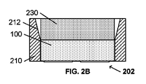
図2Bに示すように、フレーム202は、フレーム210への発光チップ100の挿入を容易にするとともに、キャップ230からの側面放射光を発光チップ100から離れるように向け直すようにも作用する、傾斜した壁セグメント212を含んでいる。
As shown in FIG. 2B, the
図2Cに示すように、フレーム203の傾斜した壁セグメント212は、フレーム210の下面まで延在している。これまた図2Cに示すように、フレーム210の開口によって形成される空洞内に液状又はペースト状の材料をディスペンスし、その後に該材料を固めることによって、キャップ230’が作り出されている。例えば、この材料は、オプションで波長変換材料を有するシリコーンとすることができ、これが、液状で塗布され、その後に硬化されて、固いキャップ230’を形成する。このような一実施形態において、この液体材料又はペースト材料は、チップ100をフレーム210に取り付ける接着剤として機能し得る。
As shown in FIG. 2C, the
図2Dに示すように、フレーム204も、空洞内にディスペンスされたキャップ230’を含んでいるが、この例においては壁213が傾斜していない。
As shown in FIG. 2D, the
図2Eに示すように、フレーム205は、チップ100とキャップ230との間に置かれた中間光学素子240を含んでいる。この光学素子240は、特有の光学効果を提供してもよいし、あるいは、チップ100の屈折率とキャップ230の屈折率との間のある屈折率を提供することによって、光取り出し効率を高めてもよい。この光学素子240は、プリフォームされた平行六面体として図示されているが、如何なる形状であってもよく、また、液状又はペースト状でディスペンスされて、その後に固められてもよい(図示せず)。フレーム210の空洞内にディスペンスされるキャップ230’の例においてのように、ディスペンスされる光学素子240は、チップ100をフレーム210に取り付けるように作用し得る。素子230、240、100とフレーム210との間に小さい隙間238が存在してもよく、あるいは、素子230、240、100のうちの1つ以上がフレーム210の内側にきつく収まっていてもよい。
As shown in FIG. 2E, the
当業者が認識するように、所望のパッケージ構築を達成するために、多様な形成・アセンブリ技術が使用され得る。図2A−2Eに示した技術のうちの一部又は全てが組み合わされてもよい。図2Fに示すように、フレーム例206は、傾斜した壁セグメント212と、プリフォームされた中間光学素子240と、液状若しくはペースト状でディスペンスされてチップ100及び光学素子240をフレーム210に取り付けるように作用するキャップ230’とを含んでいる。
As those skilled in the art will appreciate, a variety of forming and assembly techniques can be used to achieve the desired package construction. Some or all of the techniques shown in FIGS. 2A-2E may be combined. As shown in FIG. 2F, the
フレーム210の開口は好ましくは、得られるデバイス200(又は201−206)のフットプリントを最小化するために、典型的に直線的である発光チップの形状に一致するような形状にされるが、その他の形状にされた開口が設けられてもよい。例えば、材料を貫く円形の孔を開ける又は掘ることの方が一般的に単純であるので、図3A−3Dに例示するように円筒形又は円錐形の孔が設けられてもよい。
The openings in the
図3Aに、そして図3Bの断面図に示すように、デバイス例301は、フレーム210と、直線的な発光チップ100及び円形のキャップ230が中に配置される円筒形の孔とを含んでいる。この実施形態例において、孔の大きさは、それが発光チップ100を囲むように、すなわち、発光チップ100の対角線が当該円筒形の孔の直径よりも小さいか等しいかであるようにされている。斯くして、直線的な孔に代わる円筒形の孔によって生じる追加のフットプリントオーバーヘッドが最小化される。一部の実施形態において、発光チップ100が円形キャップ230に予め取り付けられ、その後、素子100、230の対が円筒形フレーム210内に配置される。チップ100とフレーム210の円筒形の壁315との間の空間は、例えばその後に硬化される誘電体ペーストなどの反射材料で充たされ得る。
As shown in FIG. 3A and in the cross-sectional view of FIG. 3B, the
図3Cに、そして図3Dの断面図に示すように、デバイス例302のフレーム210は、フレーム210の底面における開口サイズがチップ100を囲んだ、円錐形の孔を含んでいる。この例において、キャップ230’は、円錐形の空洞内に液状又はペースト状でディスペンスされてその後に硬化され、チップ100をフレーム210に取り付けるように作用し得る。オプションとして、壁325は反射性とし得る。
As shown in FIG. 3C and in the cross-sectional view of FIG. 3D, the
上述のように、図4のフレーム400は、個片化されたモジュールの各々が複数の発光チップを含むように構成されてスライス/ダイシングされてもよい。例えば自動車の照明モジュールなどの高パワー用途では、一般に複数のチップモジュールが使用される。
As described above, the
図5A−5Bは、発光モジュール内に複数の発光ダイオードを含んだ発光モジュール例を示している。これらの例において、発光モジュール501、502は、キャップ230を備えた4つの発光チップ100の行を1行以上有している。すなわち、モジュール501、502は、4つのチップ100を有する‘リニア’光ストリップ、又はチップ100の‘M×N’アレイとし得る。変数M又はNは、4であってもよいし、その他の好適な整数であってもよい。
5A-5B show an example of a light emitting module including a plurality of light emitting diodes in the light emitting module. In these examples, the
自動車の照明用途の例において、フレーム内に画成された孔の中にチップ100を配置することは、特定の自動車ランプに必要とされ得る高いアライメント精度を達成する単純な方法を提供する。
In the example of automotive lighting applications, placing the
図5Aは、フレーム510に先ず各発光チップ100が挿入され、対応するキャップ230が続くフレーム510を示している。
FIG. 5A shows the
図5Bは、フレーム510に先ずキャップ230が挿入され、発光チップ100の‘フェイスダウン’挿入が続く同じフレーム510を示している。この方法は、発光チップ100の突出したコンタクトとは対照的に、キャップ230がフレーム510と同じ高さの表面を提供するという利点をもたらす。これは、アセンブリプロセスを単純化し得るとともに、最初に挿入される素子がアセンブリプロセス中にその上で支持される表面を提供する取り外し可能なシート(図2B中の280)として使用される材料の選択に関して、より広範な選択肢をもたらし得る。すなわち、図1Cに示したようにシート280がコンタクト130を受け入れるように伸縮可能であるという要件が排除される。
FIG. 5B shows the
図6は、代替的なアセンブリ方法の一例を示している。この例においては、キャップ230がフレーム610内に配置され、発光チップ100が、例えば印刷回路基板などの基板650に取り付けられる。発光チップ100を基板650に取り付けた後に、キャップ230を備えたフレーム610が基板上に配置される。
FIG. 6 shows an example of an alternative assembly method. In this example, the
図6はマルチチップモジュール601を示しているが、当業者が認識するように、同様にしてシングルチップモジュールが組み立てられてもよい。 Although FIG. 6 shows a multi-chip module 601, single-chip modules may be assembled in a similar manner, as those skilled in the art will recognize.
図面及び以上の記載にて本発明を詳細に図示して説明してきたが、これらの図示及び説明は、限定的なものではなく、例示的あるいは典型的なものとみなされるべきであり、本発明は、開示した実施形態に限定されるものではない。 While the invention has been illustrated and described in detail in the drawings and foregoing description, such illustration and description are to be considered illustrative or exemplary and not restrictive; Is not limited to the disclosed embodiments.
例えば、図面は、素子100、230、240の全てを包囲するフレーム210を例示しているが、キャップ230の一部又は全体がフレーム210の上方まで延在して特定の光学効果を提供するような形状にされる実施形態で、本発明を処理することが可能である。例えば、キャップ230は、マッシュルーム形状であって、その上部がより広い分布の放射光を提供してもよい。同様に、光学素子240の一部又は全体がフレーム210の上方まで延在してもよく、そして、キャップ230が、フレーム210を超えて延在している光学素子240の部分を封入してもよい。また、キャップ230が省略されてもよく、そして、光学素子240が、上述の所望の光学効果を提供するような形状にされてもよい。
For example, the drawings illustrate a
開示した実施形態へのその他の変形が、図面、本開示及び添付の請求項の検討から、請求項に係る発明を実施する当業者によって理解されて実現され得る。請求項において、用語“有する”はその他の要素又はステップを排除するものではなく、不定冠詞“a”又は“an”は複数であることを排除するものではない。複数の特定の手段が互いに異なる従属請求項に記載されているという単なる事実は、それらの手段の組み合わせが有利に使用され得ないということを指し示すものではない。請求項中の如何なる参照符号も、範囲を限定するものとして解されるべきでない。 Other variations to the disclosed embodiments can be understood and realized by those skilled in the art practicing the claimed invention, from a study of the drawings, the present disclosure, and the appended claims. In the claims, the term “comprising” does not exclude other elements or steps, and the indefinite article “a” or “an” does not exclude a plurality. The mere fact that certain measures are recited in mutually different dependent claims does not indicate that a combination of these measured cannot be used to advantage. Any reference signs in the claims should not be construed as limiting the scope.
Claims (20)
貫通孔を画成したフレームと、
前記貫通孔の中に固定された発光チップであり、当該発光チップは、前記貫通孔の1つ以上の壁と直に接触した1つ以上の側面を有し、当該発光チップは、
基板と、
前記基板上の発光素子であり、n型半導体とp型半導体との間に挟まれた活性領域を有する発光素子と、
前記基板とは反対側の前記発光素子の表面上のコンタクトパッドであり、少なくとも第1のコンタクトパッドが前記n型半導体に接続され且つ第2のコンタクトパッドが前記p型半導体に接続されている、コンタクトパッドと
を有する、発光チップと、
前記貫通孔の中に固定されたキャップと
を有するデバイス。 A light emitting device,
A frame defining a through hole;
A light emitting chip fixed in the through hole, the light emitting chip having one or more side surfaces in direct contact with one or more walls of the through hole;
A substrate,
A light emitting device on the substrate, the light emitting device having an active region sandwiched between an n-type semiconductor and a p-type semiconductor;
A contact pad on the surface of the light emitting element opposite to the substrate, wherein at least a first contact pad is connected to the n-type semiconductor and a second contact pad is connected to the p-type semiconductor; A light-emitting chip having a contact pad;
A device having a cap fixed in the through hole.
前記貫通孔は、前記貫通孔内での前記キャップ又は前記発光チップの位置を制御する制限を前記貫通孔内に導入する段差形状を含む、
請求項8に記載のデバイス。 The cap is a preformed element, and the through hole includes a step shape that introduces a restriction to control the position of the cap or the light emitting chip in the through hole into the through hole.
The device of claim 8.
複数の貫通孔を含んだフレームと、
前記複数の貫通孔内に位置する複数の発光チップであり、当該発光チップの各々が、対応する貫通孔の1つ以上の壁と直に接触した1つ以上の側面を有し、当該発光チップの各々が、
基板と、
前記基板上に位置して、前記基板を通じて光を放つ発光素子と、
前記基板とは反対側である前記発光素子の表面上に形成されたコンタクトパッドと
を有する、半導体チップと、
前記複数の貫通孔の中に固定された複数のキャップと
を有し、
前記貫通孔の各々が、前記コンタクトパッドへの直接的な外部コンタクトを可能にし、且つ前記基板からの光が当該フレーム構造を出て行くことを可能にする、
フレーム構造。 A frame structure,
A frame including a plurality of through holes;
A plurality of light emitting chips located in the plurality of through holes, each of the light emitting chips having one or more side surfaces in direct contact with one or more walls of the corresponding through hole, and the light emitting chips Each of
A substrate,
A light emitting device located on the substrate and emitting light through the substrate;
A semiconductor chip having a contact pad formed on the surface of the light emitting element opposite to the substrate;
A plurality of caps fixed in the plurality of through holes;
Each of the through holes allows direct external contact to the contact pad and allows light from the substrate to exit the frame structure;
Frame structure.
各貫通孔が、該貫通孔内での対応するキャップ又は発光チップの位置を制御する制限を該貫通孔内に導入する段差形状を含む、
請求項14に記載のフレーム構造。 Each cap is a preformed element, and each through hole includes a stepped shape that introduces a restriction into the through hole that controls the position of the corresponding cap or light emitting chip within the through hole.
The frame structure according to claim 14.
複数の貫通孔を含んだフレーム構造を用意することと、
前記貫通孔の各々内に発光チップを配置することであり、前記発光チップの各々が、対応する貫通孔の1つ以上の壁と直に接触する1つ以上の側面を有し、前記発光チップの各々が、
基板と、
前記基板上に位置して、前記基板を通じて光を放つ発光素子と、
前記基板とは反対側である前記発光素子の表面上に形成されたコンタクトパッドと
を含む、配置することと、
前記貫通孔の各々内にキャップを配置することと、
前記フレーム構造をスライスして、1つ以上の発光チップを各々が含んだ個々の発光モジュールを提供することであり、各貫通孔が、前記コンタクトパッドへの直接的な外部コンタクトを可能にし、且つ前記基板からの光が対応する発光モジュールを出て行くことを可能にする、スライスすることと
を有する方法。 A method of forming a light emitting module comprising:
Preparing a frame structure including a plurality of through holes;
A light emitting chip is disposed in each of the through holes, each of the light emitting chips having one or more side surfaces in direct contact with one or more walls of the corresponding through hole; Each of
A substrate,
A light emitting device located on the substrate and emitting light through the substrate;
Including a contact pad formed on the surface of the light emitting element opposite to the substrate; and
Placing a cap within each of the through holes;
Slicing the frame structure to provide individual light emitting modules each including one or more light emitting chips, each through hole allowing direct external contact to the contact pad; and Slicing, allowing light from the substrate to exit the corresponding light emitting module.
Applications Claiming Priority (5)
| Application Number | Priority Date | Filing Date | Title |
|---|---|---|---|
| US201361877434P | 2013-09-13 | 2013-09-13 | |
| US61/877,434 | 2013-09-13 | ||
| US201461936360P | 2014-02-06 | 2014-02-06 | |
| US61/936,360 | 2014-02-06 | ||
| PCT/IB2014/064106 WO2015036887A1 (en) | 2013-09-13 | 2014-08-28 | Frame based package for flip-chip led |
Publications (3)
| Publication Number | Publication Date |
|---|---|
| JP2016536804A JP2016536804A (en) | 2016-11-24 |
| JP2016536804A5 JP2016536804A5 (en) | 2017-07-27 |
| JP6263628B2 true JP6263628B2 (en) | 2018-01-17 |
Family
ID=51743501
Family Applications (1)
| Application Number | Title | Priority Date | Filing Date |
|---|---|---|---|
| JP2016542405A Active JP6263628B2 (en) | 2013-09-13 | 2014-08-28 | Frame-based package for flip chip LEDs |
Country Status (6)
| Country | Link |
|---|---|
| US (2) | US9698323B2 (en) |
| EP (1) | EP3044809B1 (en) |
| JP (1) | JP6263628B2 (en) |
| KR (1) | KR102264061B1 (en) |
| CN (1) | CN105706237B (en) |
| WO (1) | WO2015036887A1 (en) |
Families Citing this family (17)
| Publication number | Priority date | Publication date | Assignee | Title |
|---|---|---|---|---|
| US9698323B2 (en) * | 2013-09-13 | 2017-07-04 | Koninklijke Philips N.V. | Frame based package for flip-chip LED |
| EP3093894B1 (en) * | 2015-05-15 | 2020-08-05 | OSRAM GmbH | A method of producing lighting devices and corresponding device |
| US10763404B2 (en) | 2015-10-05 | 2020-09-01 | Maven Optronics Co., Ltd. | Light emitting device with beveled reflector and manufacturing method of the same |
| JP2017116372A (en) * | 2015-12-24 | 2017-06-29 | 日東電工株式会社 | Method for inspecting optical semiconductor element having phosphor layer |
| KR20180100157A (en) | 2015-12-29 | 2018-09-07 | 루미리즈 홀딩 비.브이. | Flip Chip LEDs with Side Reflectors and Phosphors |
| DE102016104202A1 (en) | 2016-03-08 | 2017-09-14 | Osram Opto Semiconductors Gmbh | Optoelectronic semiconductor device |
| DE102016112293A1 (en) * | 2016-07-05 | 2018-01-11 | Osram Opto Semiconductors Gmbh | METHOD FOR PRODUCING AN OPTOELECTRONIC COMPONENT AND OPTOELECTRONIC COMPONENT |
| DE102016115629A1 (en) | 2016-08-23 | 2018-03-01 | Osram Opto Semiconductors Gmbh | METHOD FOR PRODUCING AN OPTOELECTRONIC COMPONENT |
| WO2018036618A1 (en) * | 2016-08-23 | 2018-03-01 | Osram Opto Semiconductors Gmbh | Method for producing a plurality of optoelectronic devices and optoelectronic device |
| DE102017103328A1 (en) * | 2017-02-17 | 2018-08-23 | Osram Opto Semiconductors Gmbh | Method for producing a conversion device with a conversion element and a litter coating |
| KR20190033979A (en) * | 2017-09-22 | 2019-04-01 | 주식회사 루멘스 | vertical type light emitting elements having color conversion electrode part |
| KR20190051205A (en) * | 2017-11-06 | 2019-05-15 | 주식회사 루멘스 | Led package |
| DE102017130574A1 (en) * | 2017-12-19 | 2019-06-19 | Osram Opto Semiconductors Gmbh | Method for producing a conversion element and conversion element |
| EP3543776A1 (en) * | 2018-03-23 | 2019-09-25 | Maven Optronics Co., Ltd. | Chip-scale linear light-emitting device |
| DE102018121338A1 (en) * | 2018-08-31 | 2020-03-05 | Osram Opto Semiconductors Gmbh | OPTOELECTRONIC LIGHTING DEVICE, OPTOELECTRONIC LIGHTING DEVICE AND MANUFACTURING METHOD |
| JP2022068684A (en) * | 2020-10-22 | 2022-05-10 | スタンレー電気株式会社 | Semiconductor light-emitting device and semiconductor light-emitting module |
| DE102022112418A1 (en) * | 2022-05-18 | 2023-11-23 | Ams-Osram International Gmbh | OPTOELECTRONIC DEVICE AND METHOD FOR PRODUCING AN OPTOELECTRONIC DEVICE |
Family Cites Families (33)
| Publication number | Priority date | Publication date | Assignee | Title |
|---|---|---|---|---|
| US5824186A (en) | 1993-12-17 | 1998-10-20 | The Regents Of The University Of California | Method and apparatus for fabricating self-assembling microstructures |
| US6184544B1 (en) * | 1998-01-29 | 2001-02-06 | Rohm Co., Ltd. | Semiconductor light emitting device with light reflective current diffusion layer |
| DE10041328B4 (en) | 2000-08-23 | 2018-04-05 | Osram Opto Semiconductors Gmbh | Packaging unit for semiconductor chips |
| JP4280050B2 (en) * | 2002-10-07 | 2009-06-17 | シチズン電子株式会社 | White light emitting device |
| JP2004192720A (en) * | 2002-12-11 | 2004-07-08 | Sankyo Seiki Mfg Co Ltd | Optical head device |
| US7517728B2 (en) * | 2004-03-31 | 2009-04-14 | Cree, Inc. | Semiconductor light emitting devices including a luminescent conversion element |
| US7456499B2 (en) * | 2004-06-04 | 2008-11-25 | Cree, Inc. | Power light emitting die package with reflecting lens and the method of making the same |
| EP1858086B1 (en) * | 2005-03-09 | 2016-11-23 | Asahi Kasei EMD Corporation | Optical device and manufacturing method of optical device |
| CN100394621C (en) * | 2005-07-29 | 2008-06-11 | 东莞市福地电子材料有限公司 | Gallium nitride based LED chip and its manufacturing method |
| WO2007147278A2 (en) * | 2006-06-21 | 2007-12-27 | Gerhard Staufert | Led light source and method |
| US7791096B2 (en) * | 2007-06-08 | 2010-09-07 | Koninklijke Philips Electronics N.V. | Mount for a semiconductor light emitting device |
| WO2013081657A1 (en) * | 2011-12-02 | 2013-06-06 | Odyne Systems, Llc | System for and method of fuel optimization in a hybrid vehicle |
| WO2009069671A1 (en) * | 2007-11-29 | 2009-06-04 | Nichia Corporation | Light-emitting device and its manufacturing method |
| CN102149965B (en) * | 2008-09-05 | 2016-08-31 | 皇家飞利浦电子股份有限公司 | Lamp assembly |
| US20100207140A1 (en) | 2009-02-19 | 2010-08-19 | Koninklijke Philips Electronics N.V. | Compact molded led module |
| JP5326705B2 (en) * | 2009-03-17 | 2013-10-30 | 日亜化学工業株式会社 | Light emitting device |
| CN101587933B (en) * | 2009-07-07 | 2010-12-08 | 苏州晶方半导体科技股份有限公司 | Wafer level encapsulating structure of a luminous diode and manufacturing method thereof |
| DE102009036621B4 (en) * | 2009-08-07 | 2023-12-21 | OSRAM Opto Semiconductors Gesellschaft mit beschränkter Haftung | Optoelectronic semiconductor component |
| KR101039881B1 (en) * | 2009-12-21 | 2011-06-09 | 엘지이노텍 주식회사 | Light emitting device and light unit using the same |
| KR100986571B1 (en) * | 2010-02-04 | 2010-10-07 | 엘지이노텍 주식회사 | Package of light emitting device and method for fabricating the same |
| DE102010025319B4 (en) * | 2010-06-28 | 2022-05-25 | OSRAM Opto Semiconductors Gesellschaft mit beschränkter Haftung | Method of manufacturing a surface mountable semiconductor device and surface mountable semiconductor devices |
| US20120074434A1 (en) * | 2010-09-24 | 2012-03-29 | Jun Seok Park | Light emitting device package and lighting apparatus using the same |
| JP5745319B2 (en) * | 2011-04-14 | 2015-07-08 | 日東電工株式会社 | Fluorescent reflection sheet and method for manufacturing light emitting diode device |
| JP5840377B2 (en) * | 2011-04-14 | 2016-01-06 | 日東電工株式会社 | Reflective resin sheet and method for manufacturing light-emitting diode device |
| KR20130014256A (en) * | 2011-07-29 | 2013-02-07 | 엘지이노텍 주식회사 | Light emitting device package and lighting system using the same |
| KR101219106B1 (en) * | 2011-08-01 | 2013-01-11 | 삼성전자주식회사 | Light emitting device package and methdod of manufacturing the same |
| WO2013056927A1 (en) * | 2011-10-20 | 2013-04-25 | Osram Gmbh | Attachment part for a support of a semiconductor light device |
| JP2013118210A (en) * | 2011-12-01 | 2013-06-13 | Citizen Holdings Co Ltd | Semiconductor light-emitting device and manufacturing method of the same |
| WO2013112435A1 (en) * | 2012-01-24 | 2013-08-01 | Cooledge Lighting Inc. | Light - emitting devices having discrete phosphor chips and fabrication methods |
| JP2014112669A (en) * | 2012-11-12 | 2014-06-19 | Citizen Holdings Co Ltd | Semiconductor light-emitting device and manufacturing method of the same |
| JP6494510B2 (en) * | 2013-07-30 | 2019-04-03 | 国立研究開発法人情報通信研究機構 | Semiconductor light emitting device and manufacturing method thereof |
| US9698323B2 (en) * | 2013-09-13 | 2017-07-04 | Koninklijke Philips N.V. | Frame based package for flip-chip LED |
| WO2015119858A1 (en) * | 2014-02-05 | 2015-08-13 | Cooledge Lighting Inc. | Light-emitting dies incorporating wavelength-conversion materials and related methods |
-
2014
- 2014-08-28 US US14/917,217 patent/US9698323B2/en active Active
- 2014-08-28 EP EP14786296.5A patent/EP3044809B1/en active Active
- 2014-08-28 WO PCT/IB2014/064106 patent/WO2015036887A1/en active Application Filing
- 2014-08-28 KR KR1020167009653A patent/KR102264061B1/en active IP Right Grant
- 2014-08-28 CN CN201480062353.2A patent/CN105706237B/en active Active
- 2014-08-28 JP JP2016542405A patent/JP6263628B2/en active Active
-
2017
- 2017-07-01 US US15/640,482 patent/US20170301841A1/en not_active Abandoned
Also Published As
| Publication number | Publication date |
|---|---|
| CN105706237A (en) | 2016-06-22 |
| US20160240755A1 (en) | 2016-08-18 |
| KR102264061B1 (en) | 2021-06-14 |
| CN105706237B (en) | 2019-10-18 |
| EP3044809B1 (en) | 2019-04-24 |
| KR20160055880A (en) | 2016-05-18 |
| WO2015036887A1 (en) | 2015-03-19 |
| US9698323B2 (en) | 2017-07-04 |
| JP2016536804A (en) | 2016-11-24 |
| EP3044809A1 (en) | 2016-07-20 |
| US20170301841A1 (en) | 2017-10-19 |
Similar Documents
| Publication | Publication Date | Title |
|---|---|---|
| JP6263628B2 (en) | Frame-based package for flip chip LEDs | |
| EP2666193B1 (en) | Led package comprising encapsulation | |
| KR102146595B1 (en) | Led with shaped growth substrate for side emission | |
| EP2979022B1 (en) | Method for manufacturing hermetically sealed illumination device with luminescent material | |
| EP2197048B1 (en) | Light-emitting device | |
| US20150085524A1 (en) | Integrated back light unit | |
| JP2014158028A (en) | Sub-mount of light emitting diode and light emitting device manufacturing method using the same | |
| KR20120119395A (en) | Light emitting device package and method of manufacturing the same | |
| JP6549043B2 (en) | LED lens for encapsulation with bottom reflector | |
| EP3022779B1 (en) | Pc led with optical element and without substrate carrier | |
| TW201322501A (en) | LED mixing chamber with reflective walls formed in slots | |
| US9209373B2 (en) | High power plastic leaded chip carrier with integrated metal reflector cup and direct heat sink | |
| WO2013118076A1 (en) | Low cost encapsulated light-emitting device | |
| KR20130127838A (en) | Light emitting device package | |
| JP2016092410A (en) | Light emitting device package and light system including the same | |
| KR20150111103A (en) | Light emitting device package | |
| KR101465708B1 (en) | Method of manufacturing a semiconductor device structure | |
| CN110391321B (en) | Light emitting diode package and method of manufacturing the same | |
| KR101461153B1 (en) | Method of manufacutruing semiconductor device structure | |
| KR20150111101A (en) | Light emitting device package | |
| KR20150111105A (en) | Light emitting device package | |
| KR20120075452A (en) | Light emitting diode having improved luminous efficiency | |
| KR20160005883A (en) | Light emitting device package |
Legal Events
| Date | Code | Title | Description |
|---|---|---|---|
| A521 | Request for written amendment filed |
Free format text: JAPANESE INTERMEDIATE CODE: A523 Effective date: 20170619 |
|
| A621 | Written request for application examination |
Free format text: JAPANESE INTERMEDIATE CODE: A621 Effective date: 20170619 |
|
| A871 | Explanation of circumstances concerning accelerated examination |
Free format text: JAPANESE INTERMEDIATE CODE: A871 Effective date: 20170619 |
|
| A975 | Report on accelerated examination |
Free format text: JAPANESE INTERMEDIATE CODE: A971005 Effective date: 20170707 |
|
| A131 | Notification of reasons for refusal |
Free format text: JAPANESE INTERMEDIATE CODE: A131 Effective date: 20170718 |
|
| A521 | Request for written amendment filed |
Free format text: JAPANESE INTERMEDIATE CODE: A523 Effective date: 20171016 |
|
| TRDD | Decision of grant or rejection written | ||
| A01 | Written decision to grant a patent or to grant a registration (utility model) |
Free format text: JAPANESE INTERMEDIATE CODE: A01 Effective date: 20171121 |
|
| A61 | First payment of annual fees (during grant procedure) |
Free format text: JAPANESE INTERMEDIATE CODE: A61 Effective date: 20171218 |
|
| R150 | Certificate of patent or registration of utility model |
Ref document number: 6263628 Country of ref document: JP Free format text: JAPANESE INTERMEDIATE CODE: R150 |
|
| S111 | Request for change of ownership or part of ownership |
Free format text: JAPANESE INTERMEDIATE CODE: R313113 |
|
| R350 | Written notification of registration of transfer |
Free format text: JAPANESE INTERMEDIATE CODE: R350 |
|
| R250 | Receipt of annual fees |
Free format text: JAPANESE INTERMEDIATE CODE: R250 |
|
| R250 | Receipt of annual fees |
Free format text: JAPANESE INTERMEDIATE CODE: R250 |
|
| R250 | Receipt of annual fees |
Free format text: JAPANESE INTERMEDIATE CODE: R250 |
|
| R250 | Receipt of annual fees |
Free format text: JAPANESE INTERMEDIATE CODE: R250 |