JP6214904B2 - Isolator circuit and semiconductor device - Google Patents
Isolator circuit and semiconductor device Download PDFInfo
- Publication number
- JP6214904B2 JP6214904B2 JP2013081959A JP2013081959A JP6214904B2 JP 6214904 B2 JP6214904 B2 JP 6214904B2 JP 2013081959 A JP2013081959 A JP 2013081959A JP 2013081959 A JP2013081959 A JP 2013081959A JP 6214904 B2 JP6214904 B2 JP 6214904B2
- Authority
- JP
- Japan
- Prior art keywords
- terminal
- transistor
- layer
- circuit
- electrically connected
- Prior art date
- Legal status (The legal status is an assumption and is not a legal conclusion. Google has not performed a legal analysis and makes no representation as to the accuracy of the status listed.)
- Expired - Fee Related
Links
Images


Classifications
-
- H—ELECTRICITY
- H01—ELECTRIC ELEMENTS
- H01L—SEMICONDUCTOR DEVICES NOT COVERED BY CLASS H10
- H01L27/00—Devices consisting of a plurality of semiconductor or other solid-state components formed in or on a common substrate
- H01L27/02—Devices consisting of a plurality of semiconductor or other solid-state components formed in or on a common substrate including semiconductor components specially adapted for rectifying, oscillating, amplifying or switching and having at least one potential-jump barrier or surface barrier; including integrated passive circuit elements with at least one potential-jump barrier or surface barrier
- H01L27/04—Devices consisting of a plurality of semiconductor or other solid-state components formed in or on a common substrate including semiconductor components specially adapted for rectifying, oscillating, amplifying or switching and having at least one potential-jump barrier or surface barrier; including integrated passive circuit elements with at least one potential-jump barrier or surface barrier the substrate being a semiconductor body
- H01L27/06—Devices consisting of a plurality of semiconductor or other solid-state components formed in or on a common substrate including semiconductor components specially adapted for rectifying, oscillating, amplifying or switching and having at least one potential-jump barrier or surface barrier; including integrated passive circuit elements with at least one potential-jump barrier or surface barrier the substrate being a semiconductor body including a plurality of individual components in a non-repetitive configuration
- H01L27/0605—Devices consisting of a plurality of semiconductor or other solid-state components formed in or on a common substrate including semiconductor components specially adapted for rectifying, oscillating, amplifying or switching and having at least one potential-jump barrier or surface barrier; including integrated passive circuit elements with at least one potential-jump barrier or surface barrier the substrate being a semiconductor body including a plurality of individual components in a non-repetitive configuration integrated circuits made of compound material, e.g. AIIIBV
-
- H—ELECTRICITY
- H01—ELECTRIC ELEMENTS
- H01L—SEMICONDUCTOR DEVICES NOT COVERED BY CLASS H10
- H01L27/00—Devices consisting of a plurality of semiconductor or other solid-state components formed in or on a common substrate
- H01L27/02—Devices consisting of a plurality of semiconductor or other solid-state components formed in or on a common substrate including semiconductor components specially adapted for rectifying, oscillating, amplifying or switching and having at least one potential-jump barrier or surface barrier; including integrated passive circuit elements with at least one potential-jump barrier or surface barrier
- H01L27/04—Devices consisting of a plurality of semiconductor or other solid-state components formed in or on a common substrate including semiconductor components specially adapted for rectifying, oscillating, amplifying or switching and having at least one potential-jump barrier or surface barrier; including integrated passive circuit elements with at least one potential-jump barrier or surface barrier the substrate being a semiconductor body
- H01L27/06—Devices consisting of a plurality of semiconductor or other solid-state components formed in or on a common substrate including semiconductor components specially adapted for rectifying, oscillating, amplifying or switching and having at least one potential-jump barrier or surface barrier; including integrated passive circuit elements with at least one potential-jump barrier or surface barrier the substrate being a semiconductor body including a plurality of individual components in a non-repetitive configuration
- H01L27/0688—Integrated circuits having a three-dimensional layout
-
- H—ELECTRICITY
- H01—ELECTRIC ELEMENTS
- H01L—SEMICONDUCTOR DEVICES NOT COVERED BY CLASS H10
- H01L27/00—Devices consisting of a plurality of semiconductor or other solid-state components formed in or on a common substrate
- H01L27/02—Devices consisting of a plurality of semiconductor or other solid-state components formed in or on a common substrate including semiconductor components specially adapted for rectifying, oscillating, amplifying or switching and having at least one potential-jump barrier or surface barrier; including integrated passive circuit elements with at least one potential-jump barrier or surface barrier
- H01L27/12—Devices consisting of a plurality of semiconductor or other solid-state components formed in or on a common substrate including semiconductor components specially adapted for rectifying, oscillating, amplifying or switching and having at least one potential-jump barrier or surface barrier; including integrated passive circuit elements with at least one potential-jump barrier or surface barrier the substrate being other than a semiconductor body, e.g. an insulating body
- H01L27/1203—Devices consisting of a plurality of semiconductor or other solid-state components formed in or on a common substrate including semiconductor components specially adapted for rectifying, oscillating, amplifying or switching and having at least one potential-jump barrier or surface barrier; including integrated passive circuit elements with at least one potential-jump barrier or surface barrier the substrate being other than a semiconductor body, e.g. an insulating body the substrate comprising an insulating body on a semiconductor body, e.g. SOI
Description
本発明は、半導体装置に関する。本明細書において、半導体装置とは、半導体素子自体または半導体素子を含むものをいい、このような半導体素子として、例えば薄膜トランジスタが挙げられる。従って、液晶表示装置及び記憶装置なども半導体装置に含まれる。 The present invention relates to a semiconductor device. In this specification, a semiconductor device refers to a semiconductor element itself or a device including a semiconductor element, and an example of such a semiconductor element is a thin film transistor. Accordingly, a liquid crystal display device, a memory device, and the like are also included in the semiconductor device.
近年、モバイルコンピュータなどの可搬型の半導体装置が急速に普及している。このような可搬型の半導体装置は蓄電部を有しており、該蓄電部からの給電により動作するが、該蓄電部の充放電容量は有限である。そのため、可能な限り消費電力を低減したいという要請がある。 In recent years, portable semiconductor devices such as mobile computers have rapidly spread. Although such a portable semiconductor device has a power storage unit and operates by power feeding from the power storage unit, the charge / discharge capacity of the power storage unit is finite. Therefore, there is a request to reduce power consumption as much as possible.
一方で、半導体装置が高性能化するに伴い、プロセッサにおける消費電力も増大してきている。そのため、処理を行っていない論理回路への給電を停止して消費電力を抑制するパワーゲーティング技術を用いることで、プロセッサの消費電力の低減を図る試みがなされている(特許文献1を参照)。 On the other hand, as the performance of semiconductor devices increases, the power consumption in the processor also increases. For this reason, attempts have been made to reduce the power consumption of the processor by using power gating technology that suppresses power consumption by stopping power supply to a logic circuit that is not performing processing (see Patent Document 1).
プロセッサにパワーゲーティング技術を適用する際に、給電が停止された論理回路と給電されている論理回路を電気的に接続する信号線があると、電源線への電流の逆流や中間電位による消費電流の増大を引き起こすおそれがある。この問題は、論理回路と信号線の間にアイソレータ回路を配することで解決することができる。 When power gating technology is applied to a processor, if there is a signal line that electrically connects the logic circuit that has been powered off to the logic circuit that is being powered, the current consumed by the current flowing back to the power line or the intermediate potential May increase. This problem can be solved by providing an isolator circuit between the logic circuit and the signal line.
本発明の一態様は、双方向の電気的な遮断が可能である新規なアイソレータ回路と、これを搭載した半導体装置を提供することを課題とする。 An object of one embodiment of the present invention is to provide a novel isolator circuit capable of bidirectional electrical interruption and a semiconductor device including the novel isolator circuit.
本発明の一態様は、片方向の電気的な遮断が可能である2つの片方向アイソレータ回路を組み合わせたアイソレータ回路である。 One embodiment of the present invention is an isolator circuit in which two unidirectional isolators that can be electrically interrupted in one direction are combined.
本発明の一態様は、論理回路と信号線が、前記構成のアイソレータ回路を介して電気的に接続されていることを特徴とする半導体装置である。 One embodiment of the present invention is a semiconductor device in which a logic circuit and a signal line are electrically connected to each other through the isolator circuit having the above structure.
本発明の一態様は、前記構成のアイソレータ回路と、論理回路と、をそれぞれ複数有し、前記論理回路の一は、前記アイソレータ回路の一を介して信号線に電気的に接続されていることを特徴とする半導体装置である。 One embodiment of the present invention includes a plurality of isolator circuits and logic circuits each having the above structure, and one of the logic circuits is electrically connected to a signal line through one of the isolator circuits. A semiconductor device characterized by the above.
双方向の電気的な遮断が可能である新規なアイソレータ回路と、これを搭載した半導体装置を得ることができる。 A novel isolator circuit capable of bidirectional electrical interruption and a semiconductor device equipped with the same can be obtained.
以下では、本発明の実施の形態について図面を用いて詳細に説明する。ただし、本発明は以下の説明に限定されず、本発明の趣旨及びその範囲から逸脱することなくその形態及び詳細を様々に変更し得ることは、当業者であれば容易に理解される。したがって、本発明は、以下に示す実施の形態の記載内容に限定して解釈されるものではない。 Hereinafter, embodiments of the present invention will be described in detail with reference to the drawings. However, the present invention is not limited to the following description, and it will be easily understood by those skilled in the art that modes and details can be variously changed without departing from the spirit and scope of the present invention. Therefore, the present invention should not be construed as being limited to the description of the embodiments below.
(実施の形態1)
本実施の形態では、本発明の一態様であるアイソレータ回路について、図1乃至図5を参照して説明する。
(Embodiment 1)
In this embodiment, an isolator circuit which is one embodiment of the present invention will be described with reference to FIGS.
図1(A)には、本発明の一態様であるアイソレータ回路として機能する回路100を示している。図1(A)の回路100は、第1の端子102及び第2の端子104に電気的に接続されている。例えば、第1の端子102は入力端子であり、第2の端子104は出力端子であるが、これに限定されず、第1の端子102が出力端子であり、第2の端子104が入力端子であってもよい。
FIG. 1A illustrates a
ここで、第1の端子102は、第1のトランジスタ106のソース及びドレインの一方に電気的に接続され、第1のトランジスタ106のソース及びドレインの他方は、第1のバッファ108の入力端子に電気的に接続され、第1のバッファ108の出力端子は、第2の端子104に電気的に接続されている。
Here, the
また、第1の端子102は、第2のバッファ110の出力端子に電気的に接続され、第2のバッファ110の入力端子は、第2のトランジスタ112のソース及びドレインの一方に電気的に接続され、第2のトランジスタ112のソース及びドレインの他方は、第2の端子104に電気的に接続されている。
The
第1のトランジスタ106のゲートは、端子114に電気的に接続されている。端子114の電位は制御可能であり、端子114の電位が高電位(H)であれば第1のトランジスタ106はオンし、端子114の電位が低電位(L)であれば第1のトランジスタ106はオフする。
The gate of the
第1のバッファ108には、端子116が電気的に接続されている。端子116の電位は制御可能であり、端子116は、後に説明する図3の第3の端子310に相当する。
A
第2のバッファ110には、端子118が電気的に接続されている。端子118の電位は制御可能であり、端子118は端子116と同様に、後に説明する図3の第3の端子310に相当する。
A
第2のトランジスタ112のゲートは、端子120に電気的に接続されている。端子120の電位は制御可能であり、端子120の電位が高電位(H)であれば第2のトランジスタ112はオンし、端子120の電位が低電位(L)であれば第2のトランジスタ112はオフする。
The gate of the
第1のトランジスタ106及び第2のトランジスタ112は、オフ電流の小さいトランジスタであればよい。
The
ここで、オフ電流の小さいトランジスタでは、チャネル幅1μmあたりのオフ電流が、10aA(1×10⁻¹⁷A)以下であるとよい。オフ電流の小さいトランジスタのチャネル幅1μmあたりのオフ電流は、1aA(1×10⁻¹⁸A)以下であることが好ましく、10zA(1×10⁻²⁰A)以下であることがより好ましく、1zA(1×10⁻²¹A)以下であることがさらに好ましく、100yA(1×10⁻²²A)以下にすることが最も好ましい。 Here, in a transistor with a small off-state current, an off-current per channel width of 1 μm is preferably 10 aA (1 × 10 −17 A) or less. The off-current per channel width of a transistor having a small off-current is preferably 1 aA (1 × 10 −18 A) or less, more preferably 10 zA (1 × 10 −20 A) or less, and 1 zA ( 1 × 10 −21 A) or less is more preferable, and 100 yA (1 × 10 −22 A) or less is most preferable.
第1のバッファ108及び第2のバッファ110は、トランジスタとバッファの間にデータ保持部を形成することができ、且つ端子116または端子118の電位が高電位(H)となることでデータ保持部のデータを第1の端子102または第2の端子104に出力することが可能な構成であればよい。このような構成は、例えばインバータとクロックドインバータを組み合わせることで実現することができる。なお、第1のバッファ108及び第2のバッファ110の具体的な構成は、図3を参照して後に説明する。なお、データ保持部は図1(A)の太線で示した部分である。
In the
図1(B)は、図1(A)に示す回路100の適用例を説明する図である。図1(B)では、第1の論理回路150と第2の論理回路152の間に回路100が配されている。
FIG. 1B illustrates an application example of the
第1の論理回路150から出力されたデータが第2の論理回路152に入力されて第2の論理回路152が処理を行う場合には、端子114、端子118及び端子120の電位を低電位(L)とし、端子116の電位を高電位(H)とする。すると、第1の論理回路150をオフしても第2の論理回路152は、第1のトランジスタ106と第1のバッファ108の間に設けられたデータ保持部のデータにより処理を続行することができる。
When data output from the
ここで、本発明の他の態様のアイソレータ回路について説明する。図2(A)には、本発明の他の態様のアイソレータ回路の例として回路200を示している。図2(A)の回路200は、第1の端子202及び第2の端子204に電気的に接続されている。
Here, an isolator circuit according to another aspect of the present invention will be described. FIG. 2A shows a
ここで、第1の端子202は、第1のトランスミッションゲート206の入力端子に電気的に接続され、第1のトランスミッションゲート206の出力端子は、第1のトランジスタ208のソース及びドレインの一方と、第2の端子204に電気的に接続されている。
Here, the
また、第1の端子202は、第2のトランジスタ210のソース及びドレインの一方と、第2のトランスミッションゲート212の出力端子に電気的に接続され、第2のトランスミッションゲート212の入力端子は、第2の端子204に電気的に接続されている。
The
なお、第1のトランスミッションゲート206及び第2のトランスミッションゲート212の入力端子と出力端子は、逆であってもよい。
Note that the input terminal and the output terminal of the
図2(B)には、第1のトランスミッションゲート206または第2のトランスミッションゲート212の具体的な構成の一例を示している。
FIG. 2B illustrates an example of a specific configuration of the
第1のトランスミッションゲート206は、第1の制御端子214及び第2の制御端子216に電気的に接続されている。第1の制御端子214及び第2の制御端子216の電位は制御可能である。
The
第1の制御端子214の電位が高電位(H)であり、第2の制御端子216の電位が低電位(L)である場合には、第1のトランスミッションゲート206中のpチャネル型トランジスタとnチャネル型トランジスタは、ともにオフする。
When the potential of the
第1の制御端子214の電位が低電位(L)であり、第2の制御端子216の電位が高電位(H)である場合には、第1のトランスミッションゲート206中のpチャネル型トランジスタとnチャネル型トランジスタは、ともにオンする。
When the potential of the
第1のトランジスタ208のゲートは端子218に電気的に接続されている。第1のトランジスタ208のソース及びドレインの他方は端子220に電気的に接続されている。端子218の電位は制御可能であり、端子218の電位を高電位(H)とすると第1のトランジスタ208はオンし、低電位(L)とすると第1のトランジスタ208はオフする。端子220は、低電位電源線Vssに電気的に接続されている。
The gate of the
第2のトランジスタ210のゲートは端子222に電気的に接続されている。第2のトランジスタ210のソース及びドレインの他方は端子224に電気的に接続されている。端子222の電位は、制御可能であり、端子222の電位を高電位(H)とすると第2のトランジスタ210はオンし、低電位(L)とすると第2のトランジスタ210はオフする。端子224は、低電位電源線Vssに電気的に接続されている。
The gate of the
第2のトランスミッションゲート212は、第1の制御端子226及び第2の制御端子228に電気的に接続されている。第1の制御端子226及び第2の制御端子228の電位は制御可能である。
The
第1の制御端子226の電位が高電位(H)であり、第2の制御端子228の電位が低電位(L)である場合には、第2のトランスミッションゲート212中のpチャネル型トランジスタとnチャネル型トランジスタは、ともにオフする。
When the potential of the
第1の制御端子226の電位が低電位(L)であり、第2の制御端子228の電位が高電位(H)である場合には、第2のトランスミッションゲート212中のpチャネル型トランジスタとnチャネル型トランジスタは、ともにオンする。
When the potential of the
図2(C)には、本発明の他の態様のアイソレータ回路の例として回路250を示している。図2(C)の回路250は第1の端子252及び第2の端子254に電気的に接続されている。
FIG. 2C illustrates a
ここで、第1の端子252は、第1の論理積回路256の入力端子の一方に電気的に接続され、第1の論理積回路256の出力端子は第2の端子254に電気的に接続されている。なお、第1の論理積回路256の入力端子の他方は、端子260に電気的に接続されている。
Here, the
また、第1の端子252は、第2の論理積回路258の出力端子に電気的に接続されている。第2の論理積回路258の入力端子の一方は第2の端子254に電気的に接続され、第2の論理積回路258の入力端子の他方は端子262に電気的に接続されている。
The
端子260及び端子262の電位は制御可能である。端子260を高電位(H)とし、第1の端子252から信号が供給される(第1の端子252が高電位(H)になる)と、この信号は第1の論理積回路256の出力端子から出力される。端子260が低電位(L)であれば、第1の端子252から信号が供給されても(第1の端子252が高電位(H)になっても)第1の論理積回路256の出力端子からは信号が出力されない。このようにして信号の伝搬を制御することができる。
The potentials of the terminal 260 and the terminal 262 can be controlled. When the terminal 260 is set to a high potential (H) and a signal is supplied from the first terminal 252 (the
しかしながら、図2(A)及び(C)に示す本発明の他の態様の構成では、データ保持部が存在しないため、電源をオフするとデータは消去される。そのため、データを保持するためには、別途データ保持部を設ける必要がある。そこで、好ましい形態として、本発明の一態様である図1(A)に示す構成を採用すると、アイソレータ回路内にデータ保持部が設けられるため、別途データ保持部を設けることなく、電源をオフしてもデータが消去されないアイソレータ回路を得ることができる。 However, in the configuration of another aspect of the present invention shown in FIGS. 2A and 2C, there is no data holding unit, and thus data is erased when the power is turned off. Therefore, it is necessary to provide a separate data holding unit in order to hold data. Therefore, as a preferable mode, when the structure illustrated in FIG. 1A which is one embodiment of the present invention is employed, a data holding portion is provided in the isolator circuit, so that the power supply is turned off without providing a separate data holding portion. However, an isolator circuit in which data is not erased can be obtained.
従って、一の論理回路(出力する側)の出力結果を用いて他の論理回路(入力される側)が処理を行っている場合に、当該出力する側の論理回路への給電を停止しても当該入力される側の論理回路が処理を続行することができる。 Therefore, when another logic circuit (input side) performs processing using the output result of one logic circuit (output side), power supply to the output logic circuit is stopped. Also, the logic circuit on the input side can continue processing.
図1(A)に示す本発明の一態様である好ましい形態は、一の論理回路(入力される側)に入力されるデータを出力する別の論理回路(出力する側)がオフされても前記一の論理回路(入力される側)が処理を続行することができる半導体装置を提供することを課題とする。 In a preferable embodiment which is one embodiment of the present invention illustrated in FIG. 1A, even when another logic circuit (output side) that outputs data input to one logic circuit (input side) is turned off, It is an object of the present invention to provide a semiconductor device in which the one logic circuit (input side) can continue processing.
図1(A)に示す本発明の一態様である好ましい形態は、一の論理回路(入力される側)に入力されるデータを別の論理回路(出力する側)から出力する場合であっても、前記一の論理回路(入力される側)に入力されるデータを出力する別の論理回路(出力する側)をオフすることができる半導体装置を提供することを課題とする。 A preferable embodiment which is one embodiment of the present invention shown in FIG. 1A is a case where data input to one logic circuit (input side) is output from another logic circuit (output side). Another object of the present invention is to provide a semiconductor device that can turn off another logic circuit (output side) that outputs data input to the one logic circuit (input side).
また、図1(A)に示す本発明の一態様である好ましい形態は、データ保持部を別途設けることなく前記課題を解決することを課題とする。 A preferable embodiment which is one embodiment of the present invention illustrated in FIG. 1A is to solve the above problem without separately providing a data holding portion.
図1(A)に示す本発明の一態様である好ましい形態は、外部にデータ保持部を別途設けることなくアイソレータ回路内にデータ保持部を設け、出力する側の論理回路に入力されるデータを該データ保持部に記憶することを特徴とする。 In a preferable mode which is one embodiment of the present invention illustrated in FIG. 1A, a data holding unit is provided in an isolator circuit without separately providing a data holding unit outside, and data input to a logic circuit on the output side is input. The data is stored in the data holding unit.
図1(A)に示す本発明の一態様である好ましい形態は、第1及び第2の端子と、第1及び第2のトランジスタと、第1及び第2のバッファと、を有し、前記第1の端子は、前記第1のトランジスタのソース及びドレインの一方と、前記第2のバッファの出力端子に電気的に接続され、前記第1のトランジスタのソース及びドレインの他方は、前記第1のバッファの入力端子に電気的に接続され、前記第2のバッファの入力端子は、前記第2のトランジスタのソース及びドレインの一方に電気的に接続され、前記第2の端子は、前記第1のバッファの出力端子と、前記第2のトランジスタのソース及びドレインの他方に電気的に接続され、前記第1及び第2のトランジスタのオフ電流は、チャネル幅1μmあたり10aA(1×10⁻¹⁷A)以下であることを特徴とするアイソレータ回路である。 A preferable embodiment of one embodiment of the present invention illustrated in FIG. 1A includes first and second terminals, first and second transistors, and first and second buffers, The first terminal is electrically connected to one of the source and drain of the first transistor and the output terminal of the second buffer, and the other of the source and drain of the first transistor is connected to the first transistor. The second buffer input terminal is electrically connected to one of a source and a drain of the second transistor, and the second terminal is electrically connected to the first terminal of the first transistor. an output terminal of the buffer, the second transistor being connected to the source and the other of the drain electrically, the first and the off-current of the second transistor, 10 aA per channel width of 1μm (1 × 10 -17 a A isolator circuit, characterized in that at most.
前記構成のアイソレータ回路において、前記第1及び第2のバッファにはインバータ及びクロックドインバータが設けられているとよい。 In the isolator circuit configured as described above, an inverter and a clocked inverter may be provided in the first and second buffers.
前記構成のアイソレータ回路において、前記第1及び第2のトランジスタは、チャネルが酸化物半導体層に形成されるとよい。 In the isolator circuit having the above structure, the first and second transistors may have a channel formed in an oxide semiconductor layer.
図1(A)に示す本発明の一態様である好ましい形態を採用すると、一の論理回路(入力される側)に入力されるデータを出力する別の論理回路(出力する側)のデータがアイソレータ回路内に設けられたデータ保持部に保持されるため、前記別の論理回路(出力する側)がオフされても前記一の論理回路(入力される側)が処理を続行することができる。 When the preferable mode which is one embodiment of the present invention illustrated in FIG. 1A is employed, data of another logic circuit (output side) that outputs data input to one logic circuit (input side) is obtained. Since the data is held in the data holding unit provided in the isolator circuit, even if the other logic circuit (output side) is turned off, the one logic circuit (input side) can continue processing. .
図1(A)に示す本発明の一態様である好ましい形態を採用すると、一の論理回路(入力される側)に入力されるデータを出力する別の論理回路(出力する側)のデータがアイソレータ回路内に設けられたデータ保持部に保持されるため、前記一の論理回路(入力される側)が処理を続行する場合であっても前記別の論理回路(出力する側)をオフすることができる。 When the preferable mode which is one embodiment of the present invention illustrated in FIG. 1A is employed, data of another logic circuit (output side) that outputs data input to one logic circuit (input side) is obtained. Since the data is held in the data holding unit provided in the isolator circuit, the other logic circuit (output side) is turned off even when the one logic circuit (input side) continues processing. be able to.
なお、図1(A)に示す本発明の一態様である好ましい形態では、データ保持部はアイソレータ回路内に設けられているため、データ保持部を別途設ける必要がない。 Note that in the preferable embodiment which is one embodiment of the present invention illustrated in FIG. 1A, the data holding portion is provided in the isolator circuit, and thus it is not necessary to separately provide the data holding portion.
図3には、図1(A)における第1のバッファ108及び第2のバッファ110の具体的な構成例として回路300を示している。図3の回路300は、第1の端子302及び第2の端子304に電気的に接続されている。
FIG. 3 shows a
図3の回路300は、第1のトランジスタ306と第2のトランジスタ308により構成されるインバータ回路と、第3のトランジスタ314、第4のトランジスタ316、第5のトランジスタ318及び第6のトランジスタ320により構成されるクロックドインバータ回路と、を有する。
3 includes an inverter circuit including a
第1の端子302は、第1のトランジスタ306のゲート及び第2のトランジスタ308のゲートに電気的に接続されている。第1のトランジスタ306のソース及びドレインの一方は、高電位電源線Vddに電気的に接続され、第1のトランジスタ306のソース及びドレインの他方は、第2のトランジスタ308のソース及びドレインの一方に電気的に接続され、第2のトランジスタ308のソース及びドレインの他方は、低電位電源線Vssに電気的に接続されている。
The
第3の端子310は、論理否定回路312の入力端子と第6のトランジスタ320のゲートに電気的に接続されている。論理否定回路312の出力端子は、第3のトランジスタ314のゲートに電気的に接続されている。
The
第4のトランジスタ316のゲート及び第5のトランジスタ318のゲートは、第1のトランジスタ306のソース及びドレインの他方と、第2のトランジスタ308のソース及びドレインの一方に電気的に接続されている。
The gate of the
第3のトランジスタ314のソース及びドレインの一方は、高電位電源線Vddに電気的に接続され、第3のトランジスタ314のソース及びドレインの他方は、第4のトランジスタ316のソース及びドレインの一方に電気的に接続され、第4のトランジスタ316のソース及びドレインの他方は、第5のトランジスタ318のソース及びドレインの一方に電気的に接続され、第5のトランジスタ318のソース及びドレインの他方は、第6のトランジスタ320のソース及びドレインの一方に電気的に接続され、第6のトランジスタ320のソース及びドレインの他方は、低電位電源線Vssに電気的に接続されている。
One of the source and the drain of the
第4のトランジスタ316のソース及びドレインの他方と第5のトランジスタ318のソース及びドレインの一方は、第2の端子304に電気的に接続されている。
The other of the source and the drain of the
なお、第1のトランジスタ306、第3のトランジスタ314及び第4のトランジスタ316は、pチャネル型トランジスタであり、第2のトランジスタ308、第5のトランジスタ318及び第6のトランジスタ320は、nチャネル型トランジスタである。
Note that the
第1の端子302は、回路300の入力端子である。第2の端子304は、回路300の出力端子である。
The
第3の端子310の電位は制御可能であり、第3の端子310は図1(A)の端子116または端子118に相当する。
The potential of the
以上説明した本発明の一態様であるアイソレータ回路は、半導体装置に適用することができる。本発明の一態様である、前記アイソレータ回路を搭載した半導体装置について以下に説明する。 The isolator circuit which is one embodiment of the present invention described above can be applied to a semiconductor device. A semiconductor device including the isolator circuit according to one embodiment of the present invention will be described below.
図4には、本発明の一態様である半導体装置として半導体装置400を示している。半導体装置400は、第1の論理回路402、第2の論理回路406及び第3の論理回路410を有する。第1の論理回路402には第1のアイソレータ回路404が電気的に接続され、第2の論理回路406には第2のアイソレータ回路408が電気的に接続され、第3の論理回路410には第3のアイソレータ回路412が電気的に接続されている。
FIG. 4 illustrates a
第1のアイソレータ回路404、第2のアイソレータ回路408及び第3のアイソレータ回路412は、図1(A)の回路100に相当する。
The
第1の論理回路402、第2の論理回路406及び第3の論理回路410は、論理回路であればよく、特定の構成に限定されるものではない。
The
半導体装置400に設けられた第1の論理回路402、第2の論理回路406及び第3の論理回路410は、それぞれ、第1のアイソレータ回路404、第2のアイソレータ回路408及び第3のアイソレータ回路412のいずれか一を介して、共有している信号線414に電気的に接続されている。すなわち、第1の論理回路402、第2の論理回路406及び第3の論理回路410は、一の信号線を共有する構成である。
A
ここで、図4のように複数の論理回路が共有する一の信号線に電気的に接続されている構成について図5を参照して説明する。 Here, a structure in which a plurality of logic circuits are electrically connected to one signal line as shown in FIG. 4 will be described with reference to FIG.
図5には、第1の論理回路402及び第1のアイソレータ回路404のみに着目してその構成を示している。第1のアイソレータ回路404は、図1(A)の回路100に相当するため、図1(A)と同じ符号を用いる。また、第1の端子502は図1(A)の第1の端子102に相当し、第2の端子504は図1(A)の第2の端子104に相当する。
FIG. 5 shows the configuration focusing on only the
第1の論理回路402をオフすることなく第1の論理回路402からのデータを信号線500に出力する場合には、端子114及び端子116の電位を高電位(H)とし、端子118及び端子120の電位を低電位(L)とする。なお、信号線500は図4に示す信号線414に相当する。
In the case where data from the
第1の論理回路402をオフすることなく第1の論理回路402が処理するデータを信号線500から入力する場合には、端子114及び端子116の電位を低電位(L)とし、端子118及び端子120の電位を高電位(H)とする。
In the case where data to be processed by the
第1の論理回路402からのデータを信号線500に出力している途中、第1の論理回路402をオフする前に、端子114、端子118及び端子120の電位を低電位(L)とし、端子116の電位を高電位(H)とする。すると、第1の論理回路402をオフしても信号線500には必要なデータが出力されることになる。または、信号線500に第1の論理回路402からの出力データが必要な場合であっても、第1の論理回路402をオフすることができる。このようにして、オフした第1の論理回路402と他のオンしている回路を電気的に遮断しつつ、第1の論理回路402の出力結果を他の回路で用いることができる。なお、信号線500に第1の論理回路402の出力が必要でない場合には端子116を低電位(L)とすればよい。
While the data from the
ただし、信号線500から第1の論理回路402にデータを入力している途中に他のオンしている回路をオフする場合には、他のオンしている回路をオフする前に端子114、端子116、端子118及び端子120のすべてを低電位(L)にする。このようにして、オフした第1の論理回路402と他のオンしている回路を電気的に遮断することができる。
However, when other circuits that are turned on are turned off while data is being input from the
以上説明したように、本発明の好ましい一態様である半導体装置は、本発明の好ましい一態様であるアイソレータ回路を有する。該アイソレータ回路を用いることで、半導体装置が有するそれぞれの論理回路をオフすることができるため、消費電力を効果的に低減することができる。このように、オフした回路とオンしている回路を電気的に遮断することで、電源線への電流の逆流や中間電位による消費電流の増大を防ぐとともに、オフした回路のオフする直前の出力結果を用いて他の回路が処理を行う事ができる。 As described above, the semiconductor device which is a preferable embodiment of the present invention includes the isolator circuit which is a preferable embodiment of the present invention. By using the isolator circuit, each logic circuit included in the semiconductor device can be turned off, so that power consumption can be effectively reduced. In this way, the circuit that is turned off and the circuit that is turned on are electrically cut off to prevent backflow of current to the power supply line and increase in current consumption due to intermediate potential, and output immediately before turning off the turned off circuit. Other circuits can perform processing using the result.
(実施の形態2)
本実施の形態では、本発明の一態様である半導体装置の構造の一例について説明する。
(Embodiment 2)
In this embodiment, an example of a structure of a semiconductor device which is one embodiment of the present invention will be described.
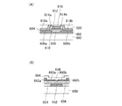
まず、本発明の一態様である半導体装置に適用可能なオフ電流の小さいトランジスタの構造の一例について、図6の断面模式図を参照して説明する。なお、図6に示す各構成要素は、実際の寸法とは異なる場合がある。 First, an example of a structure of a transistor with low off-state current that can be used in the semiconductor device which is one embodiment of the present invention is described with reference to a schematic cross-sectional view in FIG. In addition, each component shown in FIG. 6 may differ from an actual dimension.
図6(A)に示すトランジスタは、半導体層604と、絶縁層610と、導電層612と、絶縁層614a及び614bと、絶縁層616と、導電層618a及び618bと、絶縁層620と、を有する。
The transistor illustrated in FIG. 6A includes a
半導体層604は、絶縁層602を介して素子被形成層600上に設けられている。なお、これに限定されず、素子被形成層600上に半導体層604が直接設けられていてもよい。
The
半導体層604は、ドーパントが添加された領域606a及び領域606bを有し、領域606a及び領域606bの間にチャネル形成領域608を有する。
The
絶縁層610は、半導体層604の一部の上に設けられている。
The insulating
導電層612は、絶縁層610を介して半導体層604に重畳して設けられている。
The
絶縁層614a及び絶縁層614bは、導電層612の側面に接して設けられたサイドウォール絶縁層である。
The insulating
絶縁層616は、導電層612上に設けられている。
The insulating
導電層618aは領域606aに接して設けられており、導電層618bは領域606bに接して設けられている。導電層618aは、絶縁層614aの側面にも接して設けられている。導電層618bは、絶縁層614bの側面にも接して設けられている。
The
絶縁層620は、導電層618a及び導電層618bの上に設けられる。
The insulating
導電層618a及び導電層618b、並びに絶縁層620は、例えば、CMP処理を行うことで形成される。
The
また、図6(B)に示すトランジスタは、導電層652と、絶縁層654と、絶縁層656と、半導体層658と、導電層660a及び導電層660bと、導電層662a及び導電層662bと、絶縁層664と、を有する。
6B includes a
導電層652は、素子被形成層650の上に設けられている。
The
絶縁層654は、素子被形成層650の上に設けられている。導電層652及び絶縁層654の表面は平坦であることが好ましい。
The insulating
導電層652及び絶縁層654は、例えば、CMP処理を行うことで形成される。
The
絶縁層656は、導電層652及び絶縁層654の上に設けられている。
The insulating
半導体層658は、絶縁層656を介して導電層652に重畳して設けられている。
The
導電層660a及び導電層660bは、半導体層658に接して設けられている。このとき、トランジスタのチャネル長に相当する導電層660aと導電層660bの間隔は、50nm未満であることが好ましい。例えば、電子ビームで露光して形成したレジストマスクを用いて導電膜の一部をエッチングすることにより、導電層660aと導電層660bの間隔を50nm未満にすることができる。また、導電層660aと導電層660bの間隔は、図6(B)に示すように、導電層662aと662bの間隔よりも短いことが好ましい。
The
導電層662aは、導電層660aの一部の上に接して設けられており、導電層662bは、導電層660bの一部の上に接して設けられている。また、導電層662a及び導電層662bの単位面積あたりの電気抵抗は、導電層660a及び660bの単位面積あたりの電気抵抗よりも低いことが好ましい。
The
絶縁層664は、半導体層658の上を覆って設けられている。
The insulating
次に、図6(A)及び(B)に示される構成要素のそれぞれについて説明する。ただし、これらの構成要素は、単層であってもよいし、複数の層が積層されたものであってもよい。 Next, each of the components shown in FIGS. 6A and 6B will be described. However, these components may be a single layer or may be a laminate of a plurality of layers.
絶縁層602は、下地層である。絶縁層602としては、例えば、酸化シリコン、窒化シリコン、酸化窒化シリコン、窒化酸化シリコン、酸化アルミニウム、窒化アルミニウム、酸化窒化アルミニウム、窒化酸化アルミニウムまたは酸化ハフニウムなどの材料により形成すればよい。
The insulating
絶縁層654は、絶縁層602と同様の材料により形成すればよい。
The insulating
半導体層604及び半導体層658は、トランジスタのチャネルが形成される層(チャネル形成層)としての機能を有する。ここで、図6(A)の半導体層604及び図6(B)の半導体層658について説明する。
The
半導体層604及び半導体層658としては、例えば酸化物半導体層を用いることができる。
As the
以下では、酸化物半導体層の構造について説明する。 Hereinafter, the structure of the oxide semiconductor layer is described.
酸化物半導体層は、単結晶酸化物半導体層と非単結晶酸化物半導体層とに大別される。非単結晶酸化物半導体層とは、非晶質酸化物半導体層、微結晶酸化物半導体層、多結晶酸化物半導体層、CAAC−OS(C Axis Aligned Crystalline Oxide Semiconductor)層などをいう。 An oxide semiconductor layer is roughly classified into a single crystal oxide semiconductor layer and a non-single crystal oxide semiconductor layer. The non-single-crystal oxide semiconductor layer refers to an amorphous oxide semiconductor layer, a microcrystalline oxide semiconductor layer, a polycrystalline oxide semiconductor layer, a CAAC-OS (C Axis Crystalline Oxide Semiconductor) layer, or the like.
非晶質酸化物半導体層は、層中における原子配列が不規則であり、結晶成分を有さない酸化物半導体層である。微小領域においても結晶部を有さず、層全体が完全な非晶質構造の酸化物半導体層が典型である。 An amorphous oxide semiconductor layer is an oxide semiconductor layer having an irregular atomic arrangement in the layer and having no crystal component. An oxide semiconductor layer which does not have a crystal part even in a minute region and has a completely amorphous structure as a whole is typical.
微結晶酸化物半導体層は、例えば、1nm以上10nm未満の大きさの微結晶(ナノ結晶ともいう。)を含む。従って、微結晶酸化物半導体層は、非晶質酸化物半導体層よりも原子配列の規則性が高い。そのため、微結晶酸化物半導体層は、非晶質酸化物半導体層よりも欠陥準位密度が低いという特徴がある。 The microcrystalline oxide semiconductor layer includes a microcrystal (also referred to as nanocrystal) with a size greater than or equal to 1 nm and less than 10 nm, for example. Therefore, the microcrystalline oxide semiconductor layer has higher regularity of atomic arrangement than the amorphous oxide semiconductor layer. Therefore, the microcrystalline oxide semiconductor layer has a feature that the density of defect states is lower than that of the amorphous oxide semiconductor layer.
CAAC−OS層は、複数の結晶部を有する酸化物半導体層の一つであり、ほとんどの結晶部は、一辺が100nm未満の立方体内に収まる大きさである。従って、CAAC−OS層に含まれる結晶部は、一辺が10nm未満、5nm未満または3nm未満の立方体内に収まる大きさの場合も含まれる。CAAC−OS層は、微結晶酸化物半導体層よりも欠陥準位密度が低いという特徴がある。以下、CAAC−OS層について詳細な説明を行う。 The CAAC-OS layer is one of oxide semiconductor layers having a plurality of crystal parts, and most of the crystal parts are large enough to fit in a cube whose one side is less than 100 nm. Therefore, the case where a crystal part included in the CAAC-OS layer fits in a cube whose one side is less than 10 nm, less than 5 nm, or less than 3 nm is included. The CAAC-OS layer is characterized by having a lower density of defect states than a microcrystalline oxide semiconductor layer. Hereinafter, the CAAC-OS layer will be described in detail.
CAAC−OS層を透過型電子顕微鏡(TEM:Transmission Electron Microscope)によって観察すると、結晶部同士の明確な境界、即ち結晶粒界(グレインバウンダリーともいう。)を確認することができない。そのため、CAAC−OS層は、結晶粒界に起因する電子移動度の低下が起こりにくいといえる。 When the CAAC-OS layer is observed with a transmission electron microscope (TEM), a clear boundary between crystal parts, that is, a crystal grain boundary (also referred to as a grain boundary) cannot be confirmed. Thus, it can be said that the CAAC-OS layer is unlikely to decrease in electron mobility due to crystal grain boundaries.
CAAC−OS層を、試料面と概略平行な方向からTEMによって観察(断面TEM観察)すると、結晶部において、金属原子が層状に配列していることを確認できる。金属原子の各層は、CAAC−OS層の層を形成する面(被形成面ともいう。)または上面の凹凸を反映した形状であり、CAAC−OS層の被形成面または上面と平行に配列する。 When the CAAC-OS layer is observed with a TEM (cross-sectional TEM observation) from a direction substantially parallel to the sample surface, it can be confirmed that metal atoms are arranged in a layered manner in the crystal part. Each layer of metal atoms has a shape that reflects unevenness of a surface (also referred to as a surface to be formed) or an upper surface of the CAAC-OS layer, and is arranged in parallel to the surface or upper surface of the CAAC-OS layer. .
一方、CAAC−OS層を、試料面と概略垂直な方向からTEMによって観察(平面TEM観察)すると、結晶部において、金属原子が三角形状または六角形状に配列していることを確認できる。しかしながら、異なる結晶部間で、金属原子の配列に規則性は見られない。 On the other hand, when the CAAC-OS layer is observed by TEM (planar TEM observation) from a direction substantially perpendicular to the sample surface, it can be confirmed that metal atoms are arranged in a triangular shape or a hexagonal shape in the crystal part. However, there is no regularity in the arrangement of metal atoms between different crystal parts.
断面TEM観察および平面TEM観察より、CAAC−OS層の結晶部は配向性を有していることがわかる。 From the cross-sectional TEM observation and the planar TEM observation, it is found that the crystal part of the CAAC-OS layer has orientation.
なお、本明細書において、「平行」とは、二つの直線が−10°以上10°以下の角度で配置されている状態をいう。従って、−5°以上5°以下の場合も含まれる。また、「垂直」とは、二つの直線が80°以上100°以下の角度で配置されている状態をいう。従って、85°以上95°以下の場合も含まれる。 In this specification, “parallel” refers to a state in which two straight lines are arranged at an angle of −10 ° to 10 °. Therefore, the case of −5 ° to 5 ° is also included. “Vertical” refers to a state in which two straight lines are arranged at an angle of 80 ° to 100 °. Therefore, the case of 85 ° to 95 ° is also included.
また、本明細書において、結晶が三方晶または菱面体晶である場合、六方晶系として表す。 In this specification, when a crystal is trigonal or rhombohedral, it is represented as a hexagonal system.
CAAC−OS層に対し、X線回折(XRD:X−Ray Diffraction)装置を用いて構造解析を行うと、例えばInGaZnO4の結晶を有するCAAC−OS層のout−of−plane法による解析では、回折角(2θ)が31°近傍にピークが現れる場合がある。このピークは、InGaZnO4の結晶の(009)面に帰属されることから、CAAC−OS層の結晶がc軸配向性を有し、c軸が被形成面または上面に概略垂直な方向を向いていることが確認できる。 When structural analysis is performed on the CAAC-OS layer using an X-ray diffraction (XRD) apparatus, for example, in the analysis of the CAAC-OS layer having an InGaZnO 4 crystal by an out-of-plane method, A peak may appear when the diffraction angle (2θ) is around 31 °. Since this peak is attributed to the (009) plane of the InGaZnO 4 crystal, the crystal of the CAAC-OS layer has c-axis orientation, and the c-axis is in a direction substantially perpendicular to the formation surface or the top surface. Can be confirmed.
一方、CAAC−OS層に対し、c軸に概略垂直な方向からX線を入射させるin−plane法による解析では、2θが56°近傍にピークが現れる場合がある。このピークは、InGaZnO4の結晶の(110)面に帰属される。InGaZnO4の単結晶酸化物半導体層であれば、2θを56°近傍に固定し、試料面の法線ベクトルを軸(φ軸)として試料を回転させながら分析(φスキャン)を行うと、(110)面と等価な結晶面に帰属されるピークが6本観察される。これに対し、CAAC−OS層の場合は、2θを56°近傍に固定してφスキャンした場合でも、明瞭なピークが現れない。 On the other hand, in an analysis by an in-plane method in which X-rays are incident on the CAAC-OS layer from a direction substantially perpendicular to the c-axis, a peak may appear when 2θ is around 56 °. This peak is attributed to the (110) plane of the InGaZnO 4 crystal. In the case of an InGaZnO 4 single crystal oxide semiconductor layer, when 2θ is fixed at around 56 ° and analysis (φ scan) is performed while rotating the sample with the normal vector of the sample surface as the axis (φ axis), Six peaks attributed to the crystal plane equivalent to the (110) plane are observed. On the other hand, in the case of a CAAC-OS layer, a peak is not clearly observed even when φ scan is performed with 2θ fixed at around 56 °.
以上のことから、CAAC−OS層では、異なる結晶部間ではa軸およびb軸の配向は不規則であるが、c軸配向性を有し、かつc軸が被形成面または上面の法線ベクトルに平行な方向を向いていることがわかる。従って、前述の断面TEM観察で確認された層状に配列した金属原子の各層は、結晶のab面に平行な面である。 From the above, in the CAAC-OS layer, the orientation of the a-axis and the b-axis is irregular between different crystal parts, but the c-axis is aligned, and the c-axis is a normal line of the formation surface or the top surface. It can be seen that the direction is parallel to the vector. Therefore, each layer of metal atoms arranged in a layer shape confirmed by the above-mentioned cross-sectional TEM observation is a plane parallel to the ab plane of the crystal.
なお、結晶部は、CAAC−OS層を形成した際、または加熱処理などの結晶化処理を行った際に形成される。上述したように、結晶のc軸は、CAAC−OS膜の被形成面または上面の法線ベクトルに平行な方向に配向する。従って、例えば、CAAC−OS層の形状をエッチングなどによって変化させた場合、結晶のc軸がCAAC−OS層の被形成面または上面の法線ベクトルと平行にならないこともある。 Note that the crystal part is formed when the CAAC-OS layer is formed or when crystallization treatment such as heat treatment is performed. As described above, the c-axis of the crystal is oriented in a direction parallel to the normal vector of the formation surface or the top surface of the CAAC-OS film. Therefore, for example, when the shape of the CAAC-OS layer is changed by etching or the like, the c-axis of the crystal may not be parallel to the normal vector of the formation surface or the top surface of the CAAC-OS layer.
また、CAAC−OS層中の結晶化度が均一でなくてもよい。例えば、CAAC−OS層の結晶部が、CAAC−OS層の上面近傍からの結晶成長によって形成される場合、上面近傍の領域は、被形成面近傍の領域よりも結晶化度が高くなることがある。また、CAAC−OS層に不純物を添加する場合、不純物が添加された領域の結晶化度が変化し、部分的に結晶化度の異なる領域が形成されることもある。 Further, the degree of crystallinity in the CAAC-OS layer is not necessarily uniform. For example, in the case where the crystal part of the CAAC-OS layer is formed by crystal growth from the vicinity of the top surface of the CAAC-OS layer, the region near the top surface can have a higher degree of crystallinity than the region near the formation surface. is there. In addition, in the case where an impurity is added to the CAAC-OS layer, the crystallinity of a region to which the impurity is added changes, and a region with a partially different crystallinity may be formed.
なお、InGaZnO4の結晶を有するCAAC−OS層のout−of−plane法による解析では、2θが31°近傍のピークの他に、2θが36°近傍にもピークが現れる場合がある。2θが36°近傍のピークは、ZnGa2O4の結晶の(311)面に帰属されることから、InGaZnO4の結晶を有するCAAC−OS層中の一部に、ZnGa2O4の結晶が含まれることを示している。CAAC−OS層は、2θが31°近傍にピークを示し、2θが36°近傍にピークを示さないことが好ましい。 Note that when the CAAC-OS layer including an InGaZnO 4 crystal is analyzed by an out-of-plane method, in addition to a peak at 2θ of around 31 °, a peak at 2θ of around 36 ° may appear. Peak of 2θ at around 36 °, from being attributed to the (311) plane of the crystal of the ZnGa 2 O 4, a part of the CAAC-OS layer having a crystal InGaZnO 4, crystals of ZnGa 2 O 4 It is included. The CAAC-OS layer preferably has a peak at 2θ of around 31 ° and no peak at 2θ of around 36 °.
CAAC−OS層を用いたトランジスタは、可視光や紫外光の照射による電気特性の変動が小さい。よって、当該トランジスタは、信頼性が高い。 In a transistor using a CAAC-OS layer, change in electrical characteristics due to irradiation with visible light or ultraviolet light is small. Therefore, the transistor has high reliability.
なお、酸化物半導体層は、例えば、非晶質酸化物半導体層、微結晶酸化物半導体層、CAAC−OS層のうち、二種以上を有する積層であってもよい。 Note that the oxide semiconductor layer may be a stacked layer including two or more of an amorphous oxide semiconductor layer, a microcrystalline oxide semiconductor layer, and a CAAC-OS layer, for example.
酸化物半導体としては、例えばインジウム及びガリウムの一方若しくは双方と、亜鉛と、を含む金属酸化物、または該金属酸化物に含まれるガリウムの一部若しくは全部の代わりに他の金属元素を含む金属酸化物などが挙げられる。 As an oxide semiconductor, for example, a metal oxide containing one or both of indium and gallium and zinc, or a metal oxide containing another metal element instead of part or all of gallium contained in the metal oxide is used. Such as things.
前記金属酸化物としては、例えばIn系金属酸化物、Zn系金属酸化物、In−Zn系金属酸化物、またはIn−Ga−Zn系金属酸化物などを用いることができる。また、前記In−Ga−Zn系金属酸化物に含まれるガリウムの一部若しくは全部の代わりに他の金属元素を含む金属酸化物を用いてもよい。 As the metal oxide, for example, an In-based metal oxide, a Zn-based metal oxide, an In—Zn-based metal oxide, an In—Ga—Zn-based metal oxide, or the like can be used. Alternatively, a metal oxide containing another metal element instead of part or all of gallium contained in the In—Ga—Zn-based metal oxide may be used.
前記他の金属元素としては、例えばガリウムよりも多くの酸素原子と結合が可能な金属元素を用いればよく、例えばチタン、ジルコニウム、ハフニウム、ゲルマニウム、及び錫のいずれか一つまたは複数の元素を用いればよい。また、前記他の金属元素としては、ランタン、セリウム、プラセオジム、ネオジム、サマリウム、ユウロピウム、ガドリニウム、テルビウム、ジスプロシウム、ホルミウム、エルビウム、ツリウム、イッテルビウム、及びルテチウムのいずれか一つまたは複数の元素を用いればよい。これらの金属元素は、スタビライザーとしての機能を有する。なお、これらの金属元素の添加量は、金属酸化物が半導体として機能することが可能な量である。ガリウムよりも多くの酸素原子と結合が可能な金属元素を用い、さらには金属酸化物中に酸素を供給することにより、金属酸化物中の酸素欠陥を少なくすることができる。 As the other metal element, for example, a metal element capable of bonding with more oxygen atoms than gallium may be used. For example, one or more elements of titanium, zirconium, hafnium, germanium, and tin are used. That's fine. In addition, as the other metal element, any one or more of lanthanum, cerium, praseodymium, neodymium, samarium, europium, gadolinium, terbium, dysprosium, holmium, erbium, thulium, ytterbium, and lutetium may be used. Good. These metal elements have a function as a stabilizer. Note that the added amount of these metal elements is an amount by which the metal oxide can function as a semiconductor. By using a metal element capable of bonding with more oxygen atoms than gallium, and further supplying oxygen into the metal oxide, oxygen defects in the metal oxide can be reduced.
例えば、前記In−Ga−Zn系金属酸化物に含まれるガリウムの全部に代えて錫を用いるとIn−Sn−Zn系金属酸化物となり、前記In−Ga−Zn系金属酸化物に含まれるガリウムの一部に代えてチタンを用いるとIn−Ti−Ga−Zn系金属酸化物となる。 For example, when tin is used instead of all of the gallium contained in the In—Ga—Zn-based metal oxide, an In—Sn—Zn-based metal oxide is obtained, and the gallium contained in the In—Ga—Zn-based metal oxide. When titanium is used in place of a part of In, a In—Ti—Ga—Zn-based metal oxide is obtained.
また、半導体層604及び半導体層658として酸化物半導体層を用いる場合、脱水化・脱水素化を行い、酸化物半導体層中の水素、水、水酸基、または水素化物(水素化合物ともいう)などの不純物を排除し、且つ酸化物半導体層に酸素を供給すると、酸化物半導体層を高純度化させることができるため好ましい。例えば、酸化物半導体層に接する層として酸素を含む層を形成して加熱処理を行うことにより、酸化物半導体層を高純度化させることができる。
Further, in the case where oxide semiconductor layers are used as the
また、成膜直後の酸化物半導体層は、化学量論的組成より酸素が多い過飽和の状態であることが好ましい。例えば、スパッタリング法を用いて酸化物半導体層を成膜する場合、成膜ガスの酸素の占める割合が多い条件で成膜することが好ましく、特に酸素雰囲気(酸素ガス100%)で成膜を行うことが好ましい。また、酸化物半導体層に十分な酸素が供給されて酸素を過飽和の状態とするために、酸化物半導体層に接する絶縁層(絶縁層602、絶縁層610、絶縁層656、絶縁層664など)として過剰酸素を含む絶縁層(SiOx(x>2))を形成してもよい。
The oxide semiconductor layer immediately after film formation is preferably in a supersaturated state with more oxygen than in the stoichiometric composition. For example, in the case where an oxide semiconductor layer is formed by a sputtering method, the film formation is preferably performed under a condition where the proportion of oxygen in the film formation gas is large, and the film formation is performed particularly in an oxygen atmosphere (
過剰酸素を含む絶縁層は、CVD法またはスパッタリング法における成膜条件を調整し、膜中に酸素を多く含ませて形成する。また、より多くの過剰酸素を絶縁層に含ませたい場合には、イオン注入法やイオンドーピング法やプラズマ処理によって酸素を添加すればよい。また、酸化物半導体層に酸素を添加してもよい。 The insulating layer containing excess oxygen is formed by adjusting film formation conditions in a CVD method or a sputtering method so that the film contains a large amount of oxygen. In addition, when it is desired to include more excess oxygen in the insulating layer, oxygen may be added by an ion implantation method, an ion doping method, or plasma treatment. Further, oxygen may be added to the oxide semiconductor layer.
また、酸化物半導体層の形成時のスパッタリング装置には、吸着型の真空ポンプを用いることが好ましい。成膜室内の残留水分は、少ないことが好ましいためである。また、スパッタリング装置にコールドトラップが備えられていてもよい。 Further, it is preferable to use an adsorption-type vacuum pump for the sputtering apparatus for forming the oxide semiconductor layer. This is because the residual moisture in the deposition chamber is preferably small. Further, the sputtering apparatus may be provided with a cold trap.
また、酸化物半導体層は、好ましくは、350℃以上基板の歪み点未満の基板温度、より好ましくは、350℃以上450℃以下の基板温度で加熱処理を行うとよい。さらに、その後の工程において加熱処理を行ってもよい。このとき、用いる加熱処理装置には特に限定はなく、電気炉を用いてもよいし、GRTA(Gas Rapid Thermal Annealing)装置またはLRTA(Lamp Rapid Thermal Annealing)装置などのRTA(Rapid Thermal Annealing)装置を用いてもよい。また、加熱処理は複数回行ってもよい。 The oxide semiconductor layer is preferably subjected to heat treatment at a substrate temperature of 350 ° C to less than a strain point of the substrate, more preferably, a substrate temperature of 350 ° C to 450 ° C. Furthermore, you may heat-process in a subsequent process. At this time, the heat treatment apparatus to be used is not particularly limited, and an electric furnace may be used, or an RTA (Rapid Thermal Annealing) apparatus such as a GRTA (Gas Rapid Thermal Annealing) apparatus or an LRTA (Lamp Rapid Thermal Annealing) apparatus. It may be used. Further, the heat treatment may be performed a plurality of times.
また、前記加熱処理を行った後、その加熱温度を維持しつつ、またはその加熱温度から降温する過程で該加熱処理を行った炉と同じ炉に高純度の酸素ガス、高純度のN2Oガス、または超乾燥エア(露点が−40℃以下、好ましくは−60℃以下の雰囲気)を導入するとよい。このとき、酸素ガスまたはN2Oガスが、水及び水素などを含まないことが好ましい。また、加熱処理の装置に導入する酸素ガスまたはN2Oガスの純度は、6N以上であるとよく、好ましくは7N以上とするとよい。すなわち、酸素ガスまたはN2Oガス中の不純物濃度は、1ppm以下、好ましくは0.1ppm以下とする。この工程により、酸化物半導体層に酸素が供給され、酸化物半導体層中の酸素欠陥を抑制することができる。なお、前記高純度の酸素ガス、高純度のN2Oガス、または超乾燥エアの導入は、前記加熱処理時に行ってもよい。 In addition, after the heat treatment, a high-purity oxygen gas, a high-purity N 2 O is added to the same furnace as the heat-treating furnace while maintaining the heating temperature or in the process of lowering the temperature from the heating temperature. Gas or ultra-dry air (an atmosphere having a dew point of −40 ° C. or lower, preferably −60 ° C. or lower) may be introduced. At this time, oxygen gas or the N 2 O gas, it is preferred not to include such as water and hydrogen. The purity of oxygen gas or N 2 O gas introduced into the heat treatment apparatus is preferably 6N or more, and more preferably 7N or more. That is, the impurity concentration in oxygen gas or N 2 O gas is 1 ppm or less, preferably 0.1 ppm or less. Through this step, oxygen is supplied to the oxide semiconductor layer, so that oxygen defects in the oxide semiconductor layer can be suppressed. Note that introduction of the high-purity oxygen gas, high-purity N 2 O gas, or ultra-dry air may be performed during the heat treatment.
高純度化させた酸化物半導体層の水素濃度のSIMS測定値は、5×10¹⁹atoms/cm3以下、好ましくは5×1018atoms/cm3以下、より好ましくは5×1017atoms/cm3以下とするとよい。 The SIMS measurement value of the hydrogen concentration of the highly purified oxide semiconductor layer is 5 × 10 19 atoms / cm 3 or less, preferably 5 × 10 18 atoms / cm 3 or less, more preferably 5 × 10 17 atoms / cm 3. It should be 3 or less.
高純度化させた酸化物半導体層を電界効果トランジスタに用いることにより、酸化物半導体層のキャリア密度を1×10¹⁴/cm3未満、好ましくは1×1012/cm3未満、さらに好ましくは1×1011/cm3未満にすることができる。このようにキャリア密度を小さくすることで、チャネル幅1μmあたりの電界効果トランジスタのオフ電流を1×10−19A(100zA)以下、より好ましくは1×10−22A(100yA)以下にまで抑えることができる。 By using the highly purified oxide semiconductor layer for a field effect transistor, the carrier density of the oxide semiconductor layer is less than 1 × 10 14 / cm 3 , preferably less than 1 × 10 12 / cm 3 , more preferably 1 It can be less than x10 11 / cm 3 . By reducing the carrier density in this way, the off-state current of the field effect transistor per channel width of 1 μm is suppressed to 1 × 10 −19 A (100 zA) or less, more preferably 1 × 10 −22 A (100 yA) or less. be able to.
領域606a及び領域606bに含まれるドーパントとしては、例えば元素周期表における13族の元素(例えば、ホウ素など)、15族の元素(例えば、窒素、リン及びヒ素など)、及び希ガス元素(例えば、ヘリウム、アルゴン及びキセノンなど)を挙げることができ、これらのいずれか一または複数を用いればよい。
Examples of the dopant included in the
絶縁層610及び絶縁層656は、トランジスタのゲート絶縁層として機能する。絶縁層610及び絶縁層656としては、例えば、酸化シリコン、窒化シリコン、酸化窒化シリコン、窒化酸化シリコン、酸化アルミニウム、窒化アルミニウム、酸化窒化アルミニウム、窒化酸化アルミニウムまたは酸化ハフニウムなどの材料を含む層を用いればよい。
The insulating
導電層612及び導電層652は、トランジスタのゲートとして機能する。導電層612及び導電層652としては、例えば、モリブデン、チタン、クロム、タンタル、マグネシウム、銀、タングステン、アルミニウム、銅、ネオジムまたはスカンジウムなどの金属材料を含む層を用いればよい。
The
絶縁層614a、絶縁層614b及び絶縁層616としては、例えば酸化シリコン、窒化シリコン、酸化窒化シリコン、窒化酸化シリコン、酸化アルミニウム、窒化アルミニウム、酸化窒化アルミニウム、窒化酸化アルミニウム、または酸化ハフニウムなどの材料を含む層を用いればよい。
As the insulating
導電層618a及び導電層618b、導電層660a及び導電層660b、並びに導電層662a及び導電層662bは、トランジスタのソースまたはドレインとして機能する。導電層618a及び導電層618b、導電層660a及び導電層660b、導電層662a及び導電層662bとしては、例えば、モリブデン、チタン、クロム、タンタル、マグネシウム、銀、タングステン、アルミニウム、銅、ネオジム、スカンジウム、またはルテニウムなどの導電性材料を含む層を用いればよい。
The
絶縁層620及び絶縁層664は、保護層として機能する。絶縁層620及び絶縁層664としては、例えば、酸化シリコン、窒化シリコン、酸化窒化シリコン、窒化酸化シリコン、酸化アルミニウム、窒化アルミニウム、酸化窒化アルミニウム、窒化酸化アルミニウム、または酸化ハフニウムなどの材料を含む層を用いることができる。
The insulating
さらに、一例として図6(A)に示すトランジスタを用いた場合の半導体装置の構造の一例について、図7を参照して説明する。図7は、本実施の形態の半導体装置の構造の一例を説明するための断面模式図である。 Further, an example of the structure of the semiconductor device in the case where the transistor illustrated in FIG. 6A is used as an example will be described with reference to FIGS. FIG. 7 is a schematic cross-sectional view for explaining an example of the structure of the semiconductor device of this embodiment.
図7に示す半導体装置は、チャネル形成層である単結晶シリコン層708を含むトランジスタ700と、絶縁層712、絶縁層714及び絶縁層716を介してトランジスタ700の上に積層され、図6(A)に示すトランジスタで構成されるトランジスタ702と、を有する。また、トランジスタ702に接して絶縁層720が設けられている。
The semiconductor device illustrated in FIG. 7 is stacked over the
単結晶シリコン層708は、絶縁層706(BOX層ともいう)を介して基板704上に設けられている。なお、基板704、絶縁層706及び単結晶シリコン層708に代えて、単結晶半導体基板における埋め込み絶縁領域に囲まれた半導体領域を用いてトランジスタ700を構成してもよい。
The single
絶縁層712は、保護層として機能する。また、絶縁層714は、保護層のみならず、平坦化層としても機能する。また、絶縁層716は、下地層として機能する。絶縁層712、絶縁層714及び絶縁層716としては、絶縁層602と同様の材料を含む層を用いればよい。
The insulating
トランジスタ702のソースまたはドレインとしての機能を有する導電層718は、トランジスタ700のゲートとして機能する導電層710に接続されている。なお、導電層718と導電層710は、複数の導電層を介して接続されていてもよい。
A
また、トランジスタ702を前記オフ電流の低いトランジスタとすることで、メモリセルのデータの保持期間を長くすることができる。
Further, when the
また、トランジスタ700を用いて、CPU及び信号処理回路などの論理回路(揮発性記憶回路を含む)を構成することができる。これにより、動作速度を速くすることができる。
In addition, a logic circuit (including a volatile memory circuit) such as a CPU and a signal processing circuit can be formed using the
図7のトランジスタ702は、実施の形態1で説明した図1(A)の第1のトランジスタ106に相当する。そして、図7のトランジスタ700は、実施の形態1で説明した図3の第1のトランジスタ306または第2のトランジスタ308に相当する。従って、図7の導電層718が、データ保持部として機能する。
A
本実施の形態にて説明したようにオフ電流の小さいトランジスタを作製することができるため、本発明の好ましい一態様である半導体装置を実現することができる。ただし、オフ電流の小さいトランジスタは、本実施の形態にて説明したものに限定されず、データ保持部に必要な時間だけデータを保持できる程度にオフ電流が小さいトランジスタであればよく、特定の構成に限定されるものではない。 Since a transistor with low off-state current can be manufactured as described in this embodiment, a semiconductor device which is a preferable embodiment of the present invention can be realized. Note that the transistor with a small off-state current is not limited to the one described in this embodiment mode, and any transistor having a small off-state current so long as it can hold data for a time required for the data holding unit may be used. It is not limited to.
100 回路
102 第1の端子
104 第2の端子
106 第1のトランジスタ
108 第1のバッファ
110 第2のバッファ
112 第2のトランジスタ
114 端子
116 端子
118 端子
120 端子
150 第1の論理回路
152 第2の論理回路
200 回路
202 第1の端子
204 第2の端子
206 第1のトランスミッションゲート
208 第1のトランジスタ
210 第2のトランジスタ
212 第2のトランスミッションゲート
214 第1の制御端子
216 第2の制御端子
218 端子
220 端子
222 端子
224 端子
226 第1の制御端子
228 第2の制御端子
250 回路
252 第1の端子
254 第2の端子
256 第1の論理積回路
258 第2の論理積回路
260 端子
262 端子
300 回路
302 第1の端子
304 第2の端子
306 第1のトランジスタ
308 第2のトランジスタ
310 第3の端子
312 論理否定回路
314 第3のトランジスタ
316 第4のトランジスタ
318 第5のトランジスタ
320 第6のトランジスタ
400 半導体装置
402 第1の論理回路
404 第1のアイソレータ回路
406 第2の論理回路
408 第2のアイソレータ回路
410 第3の論理回路
412 第3のアイソレータ回路
414 信号線
500 信号線
502 第1の端子
504 第2の端子
600 素子被形成層
602 絶縁層
604 半導体層
606a 領域
606b 領域
608 チャネル形成領域
610 絶縁層
612 導電層
614a 絶縁層
614b 絶縁層
616 絶縁層
618a 導電層
618b 導電層
620 絶縁層
650 素子被形成層
652 導電層
654 絶縁層
656 絶縁層
658 半導体層
660a 導電層
660b 導電層
662a 導電層
662b 導電層
664 絶縁層
700 トランジスタ
702 トランジスタ
704 基板
706 絶縁層
708 単結晶シリコン層
710 導電層
712 絶縁層
714 絶縁層
716 絶縁層
718 導電層
720 絶縁層
100 circuit 102 1st terminal 104 2nd terminal 106 1st transistor 108 1st buffer 110 2nd buffer 112 2nd transistor 114 terminal 116 terminal 118 terminal 120 terminal 150 1st logic circuit 152 2nd logic Logic circuit 200 circuit 202 first terminal 204 second terminal 206 first transmission gate 208 first transistor 210 second transistor 212 second transmission gate 214 first control terminal 216 second control terminal 218 terminal 220 terminal 222 terminal 224 terminal 226 first control terminal 228 second control terminal 250 circuit 252 first terminal 254 second terminal 256 first AND circuit 258 second AND circuit 260 terminal 262 terminal 300 circuit 302 First terminal 304 Second terminal 06 1st transistor 308 2nd transistor 310 3rd terminal 312 Logic negation circuit 314 3rd transistor 316 4th transistor 318 5th transistor 320 6th transistor 400 Semiconductor device 402 1st logic circuit 404 1st One isolator circuit 406 Second logic circuit 408 Second isolator circuit 410 Third logic circuit 412 Third isolator circuit 414 Signal line 500 Signal line 502 First terminal 504 Second terminal 600 Element formation layer 602 Insulating layer 604 Semiconductor layer 606a Region 606b Region 608 Channel formation region 610 Insulating layer 612 Conductive layer 614a Insulating layer 614b Insulating layer 616 Insulating layer 618a Conductive layer 618b Conductive layer 620 Insulating layer 650 Element formation layer 652 Conductive layer 654 Insulating layer 656 Insulating layer layer 58 semiconductor layer 660a conductive layer 660b conductive layer 662a conductive layer 662b conductive layer 664 insulating layer 700 the transistor 702 the transistor 704 substrate 706 insulating layer 708 single crystal silicon layer 710 conductive layer 712 insulating layer 714 insulating layer 716 insulating layer 718 conductive layer 720 insulating layer
Claims (4)
前記第1の端子は、前記第1のトランジスタのソース及びドレインの一方と、前記第2のバッファの出力端子に電気的に接続され、
前記第1のトランジスタのソース及びドレインの他方は、前記第1のバッファの入力端子に電気的に接続され、
前記第2のバッファの入力端子は、前記第2のトランジスタのソース及びドレインの一方に電気的に接続され、
前記第2の端子は、前記第1のバッファの出力端子と、前記第2のトランジスタのソース及びドレインの他方に電気的に接続され、
前記第1及び第2のトランジスタのオフ電流は、チャネル幅1μmあたり1×10⁻¹⁷A以下であり、
前記第1及び第2のトランジスタは、チャネルが形成される領域に非単結晶の酸化物半導体を有し、
前記チャネルが形成される領域は、c軸配向した結晶を有し、透過型電子顕微鏡を用いた観察によって結晶粒界が確認されない領域を有することを特徴とするアイソレータ回路。 First and second terminals, first and second transistors, and first and second buffers,
The first terminal is electrically connected to one of a source and a drain of the first transistor and an output terminal of the second buffer;
The other of the source and the drain of the first transistor is electrically connected to the input terminal of the first buffer;
An input terminal of the second buffer is electrically connected to one of a source and a drain of the second transistor;
The second terminal is electrically connected to the output terminal of the first buffer and the other of the source and the drain of the second transistor;
Wherein the first and the off-current of the second transistor, Ri 1 × 10 -17 A der less per channel width 1 [mu] m,
The first and second transistors each include a non-single-crystal oxide semiconductor in a region where a channel is formed;
The isolator circuit is characterized in that the region where the channel is formed has a c-axis oriented crystal and has a region where a crystal grain boundary is not confirmed by observation using a transmission electron microscope .
前記第1及び第2のバッファにはインバータ及びクロックドインバータが設けられていることを特徴とするアイソレータ回路。 In claim 1,
An isolator circuit comprising an inverter and a clocked inverter provided in the first and second buffers .
前記論理回路の一は、前記アイソレータ回路の一を介して信号線に電気的に接続されていることを特徴とする半導体装置。 The isolator circuit according to claim 1 or 2 and a plurality of logic circuits, respectively,
One of the logic circuits is electrically connected to a signal line through one of the isolator circuits.
Priority Applications (1)
| Application Number | Priority Date | Filing Date | Title |
|---|---|---|---|
| JP2013081959A JP6214904B2 (en) | 2012-04-13 | 2013-04-10 | Isolator circuit and semiconductor device |
Applications Claiming Priority (3)
| Application Number | Priority Date | Filing Date | Title |
|---|---|---|---|
| JP2012091727 | 2012-04-13 | ||
| JP2012091727 | 2012-04-13 | ||
| JP2013081959A JP6214904B2 (en) | 2012-04-13 | 2013-04-10 | Isolator circuit and semiconductor device |
Publications (2)
| Publication Number | Publication Date |
|---|---|
| JP2013236365A JP2013236365A (en) | 2013-11-21 |
| JP6214904B2 true JP6214904B2 (en) | 2017-10-18 |
Family
ID=49324273
Family Applications (1)
| Application Number | Title | Priority Date | Filing Date |
|---|---|---|---|
| JP2013081959A Expired - Fee Related JP6214904B2 (en) | 2012-04-13 | 2013-04-10 | Isolator circuit and semiconductor device |
Country Status (2)
| Country | Link |
|---|---|
| US (1) | US9030232B2 (en) |
| JP (1) | JP6214904B2 (en) |
Families Citing this family (8)
| Publication number | Priority date | Publication date | Assignee | Title |
|---|---|---|---|---|
| JP6396671B2 (en) | 2013-04-26 | 2018-09-26 | 株式会社半導体エネルギー研究所 | Semiconductor device |
| JP6106024B2 (en) * | 2013-05-21 | 2017-03-29 | 株式会社ジャパンディスプレイ | Thin film transistor manufacturing method and thin film transistor |
| DE102016207737A1 (en) * | 2015-05-11 | 2016-11-17 | Semiconductor Energy Laboratory Co., Ltd. | Semiconductor device, method for manufacturing the semiconductor device, tire and moving object |
| US9627275B1 (en) * | 2015-10-30 | 2017-04-18 | Taiwan Semiconductor Manufacturing Company Ltd. | Hybrid semiconductor structure on a common substrate |
| CN109478883A (en) | 2016-07-19 | 2019-03-15 | 株式会社半导体能源研究所 | Semiconductor device |
| US10120470B2 (en) | 2016-07-22 | 2018-11-06 | Semiconductor Energy Laboratory Co., Ltd. | Semiconductor device, display device and electronic device |
| WO2018122658A1 (en) | 2016-12-27 | 2018-07-05 | Semiconductor Energy Laboratory Co., Ltd. | Semiconductor device |
| US11538804B2 (en) * | 2019-01-09 | 2022-12-27 | Intel Corporation | Stacked integration of III-N transistors and thin-film transistors |
Family Cites Families (115)
| Publication number | Priority date | Publication date | Assignee | Title |
|---|---|---|---|---|
| JPS59225422A (en) * | 1983-06-03 | 1984-12-18 | Toshiba Corp | Bidirectional bus buffer |
| JPS60198861A (en) | 1984-03-23 | 1985-10-08 | Fujitsu Ltd | Thin film transistor |
| JPH0244256B2 (en) | 1987-01-28 | 1990-10-03 | Kagaku Gijutsucho Mukizaishitsu Kenkyushocho | INGAZN2O5DESHIMESARERUROTSUHOSHOKEINOSOJOKOZOOJUSURUKAGOBUTSUOYOBISONOSEIZOHO |
| JPS63210023A (en) | 1987-02-24 | 1988-08-31 | Natl Inst For Res In Inorg Mater | Compound having laminar structure of hexagonal crystal system expressed by ingazn4o7 and its production |
| JPH0244260B2 (en) | 1987-02-24 | 1990-10-03 | Kagaku Gijutsucho Mukizaishitsu Kenkyushocho | INGAZN5O8DESHIMESARERUROTSUHOSHOKEINOSOJOKOZOOJUSURUKAGOBUTSUOYOBISONOSEIZOHO |
| JPH0244258B2 (en) | 1987-02-24 | 1990-10-03 | Kagaku Gijutsucho Mukizaishitsu Kenkyushocho | INGAZN3O6DESHIMESARERUROTSUHOSHOKEINOSOJOKOZOOJUSURUKAGOBUTSUOYOBISONOSEIZOHO |
| JPH0244262B2 (en) | 1987-02-27 | 1990-10-03 | Kagaku Gijutsucho Mukizaishitsu Kenkyushocho | INGAZN6O9DESHIMESARERUROTSUHOSHOKEINOSOJOKOZOOJUSURUKAGOBUTSUOYOBISONOSEIZOHO |
| JPH0244263B2 (en) | 1987-04-22 | 1990-10-03 | Kagaku Gijutsucho Mukizaishitsu Kenkyushocho | INGAZN7O10DESHIMESARERUROTSUHOSHOKEINOSOJOKOZOOJUSURUKAGOBUTSUOYOBISONOSEIZOHO |
| JPH05251705A (en) | 1992-03-04 | 1993-09-28 | Fuji Xerox Co Ltd | Thin-film transistor |
| JPH08106345A (en) * | 1994-10-05 | 1996-04-23 | Fujitsu Ltd | Interface device between different voltage elements |
| JP3479375B2 (en) | 1995-03-27 | 2003-12-15 | 科学技術振興事業団 | Metal oxide semiconductor device in which a pn junction is formed with a thin film transistor made of a metal oxide semiconductor such as cuprous oxide, and methods for manufacturing the same |
| DE69635107D1 (en) | 1995-08-03 | 2005-09-29 | Koninkl Philips Electronics Nv | SEMICONDUCTOR ARRANGEMENT WITH A TRANSPARENT CIRCUIT ELEMENT |
| JP3625598B2 (en) | 1995-12-30 | 2005-03-02 | 三星電子株式会社 | Manufacturing method of liquid crystal display device |
| JP4170454B2 (en) | 1998-07-24 | 2008-10-22 | Hoya株式会社 | Article having transparent conductive oxide thin film and method for producing the same |
| JP2000150861A (en) | 1998-11-16 | 2000-05-30 | Tdk Corp | Oxide thin film |
| JP3276930B2 (en) | 1998-11-17 | 2002-04-22 | 科学技術振興事業団 | Transistor and semiconductor device |
| TW460731B (en) | 1999-09-03 | 2001-10-21 | Ind Tech Res Inst | Electrode structure and production method of wide viewing angle LCD |
| JP4089858B2 (en) | 2000-09-01 | 2008-05-28 | 国立大学法人東北大学 | Semiconductor device |
| KR20020038482A (en) | 2000-11-15 | 2002-05-23 | 모리시타 요이찌 | Thin film transistor array, method for producing the same, and display panel using the same |
| JP3997731B2 (en) | 2001-03-19 | 2007-10-24 | 富士ゼロックス株式会社 | Method for forming a crystalline semiconductor thin film on a substrate |
| JP2002289859A (en) | 2001-03-23 | 2002-10-04 | Minolta Co Ltd | Thin-film transistor |
| JP4090716B2 (en) | 2001-09-10 | 2008-05-28 | 雅司 川崎 | Thin film transistor and matrix display device |
| JP3925839B2 (en) | 2001-09-10 | 2007-06-06 | シャープ株式会社 | Semiconductor memory device and test method thereof |
| US7061014B2 (en) | 2001-11-05 | 2006-06-13 | Japan Science And Technology Agency | Natural-superlattice homologous single crystal thin film, method for preparation thereof, and device using said single crystal thin film |
| JP4164562B2 (en) | 2002-09-11 | 2008-10-15 | 独立行政法人科学技術振興機構 | Transparent thin film field effect transistor using homologous thin film as active layer |
| JP4083486B2 (en) | 2002-02-21 | 2008-04-30 | 独立行政法人科学技術振興機構 | Method for producing LnCuO (S, Se, Te) single crystal thin film |
| US7049190B2 (en) | 2002-03-15 | 2006-05-23 | Sanyo Electric Co., Ltd. | Method for forming ZnO film, method for forming ZnO semiconductor layer, method for fabricating semiconductor device, and semiconductor device |
| JP3933591B2 (en) | 2002-03-26 | 2007-06-20 | 淳二 城戸 | Organic electroluminescent device |
| US7339187B2 (en) | 2002-05-21 | 2008-03-04 | State Of Oregon Acting By And Through The Oregon State Board Of Higher Education On Behalf Of Oregon State University | Transistor structures |
| JP2004022625A (en) | 2002-06-13 | 2004-01-22 | Murata Mfg Co Ltd | Manufacturing method of semiconductor device and its manufacturing method |
| US7105868B2 (en) | 2002-06-24 | 2006-09-12 | Cermet, Inc. | High-electron mobility transistor with zinc oxide |
| US7067843B2 (en) | 2002-10-11 | 2006-06-27 | E. I. Du Pont De Nemours And Company | Transparent oxide semiconductor thin film transistors |
| JP4166105B2 (en) | 2003-03-06 | 2008-10-15 | シャープ株式会社 | Semiconductor device and manufacturing method thereof |
| JP2004273732A (en) | 2003-03-07 | 2004-09-30 | Sharp Corp | Active matrix substrate and its producing process |
| WO2004100473A2 (en) * | 2003-04-30 | 2004-11-18 | Analog Devices, Inc. | Signal isolators using micro-transformers |
| JP4108633B2 (en) | 2003-06-20 | 2008-06-25 | シャープ株式会社 | THIN FILM TRANSISTOR, MANUFACTURING METHOD THEREOF, AND ELECTRONIC DEVICE |
| US7262463B2 (en) | 2003-07-25 | 2007-08-28 | Hewlett-Packard Development Company, L.P. | Transistor including a deposited channel region having a doped portion |
| US20050093577A1 (en) * | 2003-11-04 | 2005-05-05 | Liem Nguyen | Multiplexer circuits |
| US7287171B1 (en) * | 2004-03-08 | 2007-10-23 | Altera Corporation | Systems and methods for reducing static and total power consumption in programmable logic device architectures |
| US20070194379A1 (en) | 2004-03-12 | 2007-08-23 | Japan Science And Technology Agency | Amorphous Oxide And Thin Film Transistor |
| US7282782B2 (en) | 2004-03-12 | 2007-10-16 | Hewlett-Packard Development Company, L.P. | Combined binary oxide semiconductor device |
| US7145174B2 (en) | 2004-03-12 | 2006-12-05 | Hewlett-Packard Development Company, Lp. | Semiconductor device |
| US7297977B2 (en) | 2004-03-12 | 2007-11-20 | Hewlett-Packard Development Company, L.P. | Semiconductor device |
| US7211825B2 (en) | 2004-06-14 | 2007-05-01 | Yi-Chi Shih | Indium oxide-based thin film transistors and circuits |
| JP2006100760A (en) | 2004-09-02 | 2006-04-13 | Casio Comput Co Ltd | Thin-film transistor and its manufacturing method |
| US7285501B2 (en) | 2004-09-17 | 2007-10-23 | Hewlett-Packard Development Company, L.P. | Method of forming a solution processed device |
| US7298084B2 (en) | 2004-11-02 | 2007-11-20 | 3M Innovative Properties Company | Methods and displays utilizing integrated zinc oxide row and column drivers in conjunction with organic light emitting diodes |
| KR100939998B1 (en) | 2004-11-10 | 2010-02-03 | 캐논 가부시끼가이샤 | Amorphous oxide and field effect transistor |
| US7863611B2 (en) | 2004-11-10 | 2011-01-04 | Canon Kabushiki Kaisha | Integrated circuits utilizing amorphous oxides |
| US7872259B2 (en) | 2004-11-10 | 2011-01-18 | Canon Kabushiki Kaisha | Light-emitting device |
| US7453065B2 (en) | 2004-11-10 | 2008-11-18 | Canon Kabushiki Kaisha | Sensor and image pickup device |
| US7829444B2 (en) | 2004-11-10 | 2010-11-09 | Canon Kabushiki Kaisha | Field effect transistor manufacturing method |
| CA2585071A1 (en) | 2004-11-10 | 2006-05-18 | Canon Kabushiki Kaisha | Field effect transistor employing an amorphous oxide |
| US7791072B2 (en) | 2004-11-10 | 2010-09-07 | Canon Kabushiki Kaisha | Display |
| US7579224B2 (en) | 2005-01-21 | 2009-08-25 | Semiconductor Energy Laboratory Co., Ltd. | Method for manufacturing a thin film semiconductor device |
| US7608531B2 (en) | 2005-01-28 | 2009-10-27 | Semiconductor Energy Laboratory Co., Ltd. | Semiconductor device, electronic device, and method of manufacturing semiconductor device |
| TWI562380B (en) | 2005-01-28 | 2016-12-11 | Semiconductor Energy Lab Co Ltd | Semiconductor device, electronic device, and method of manufacturing semiconductor device |
| US7858451B2 (en) | 2005-02-03 | 2010-12-28 | Semiconductor Energy Laboratory Co., Ltd. | Electronic device, semiconductor device and manufacturing method thereof |
| US7948171B2 (en) | 2005-02-18 | 2011-05-24 | Semiconductor Energy Laboratory Co., Ltd. | Light emitting device |
| US20060197092A1 (en) | 2005-03-03 | 2006-09-07 | Randy Hoffman | System and method for forming conductive material on a substrate |
| US8681077B2 (en) | 2005-03-18 | 2014-03-25 | Semiconductor Energy Laboratory Co., Ltd. | Semiconductor device, and display device, driving method and electronic apparatus thereof |
| WO2006105077A2 (en) | 2005-03-28 | 2006-10-05 | Massachusetts Institute Of Technology | Low voltage thin film transistor with high-k dielectric material |
| US7645478B2 (en) | 2005-03-31 | 2010-01-12 | 3M Innovative Properties Company | Methods of making displays |
| US8300031B2 (en) | 2005-04-20 | 2012-10-30 | Semiconductor Energy Laboratory Co., Ltd. | Semiconductor device comprising transistor having gate and drain connected through a current-voltage conversion element |
| JP2006344849A (en) | 2005-06-10 | 2006-12-21 | Casio Comput Co Ltd | Thin film transistor |
| US7691666B2 (en) | 2005-06-16 | 2010-04-06 | Eastman Kodak Company | Methods of making thin film transistors comprising zinc-oxide-based semiconductor materials and transistors made thereby |
| US7402506B2 (en) | 2005-06-16 | 2008-07-22 | Eastman Kodak Company | Methods of making thin film transistors comprising zinc-oxide-based semiconductor materials and transistors made thereby |
| US7507618B2 (en) | 2005-06-27 | 2009-03-24 | 3M Innovative Properties Company | Method for making electronic devices using metal oxide nanoparticles |
| KR100711890B1 (en) | 2005-07-28 | 2007-04-25 | 삼성에스디아이 주식회사 | Organic Light Emitting Display and Fabrication Method for the same |
| JP2007059128A (en) | 2005-08-23 | 2007-03-08 | Canon Inc | Organic electroluminescent display device and manufacturing method thereof |
| JP2007073705A (en) | 2005-09-06 | 2007-03-22 | Canon Inc | Oxide-semiconductor channel film transistor and its method of manufacturing same |
| JP4850457B2 (en) | 2005-09-06 | 2012-01-11 | キヤノン株式会社 | Thin film transistor and thin film diode |
| JP5116225B2 (en) | 2005-09-06 | 2013-01-09 | キヤノン株式会社 | Manufacturing method of oxide semiconductor device |
| JP4280736B2 (en) | 2005-09-06 | 2009-06-17 | キヤノン株式会社 | Semiconductor element |
| EP1998373A3 (en) | 2005-09-29 | 2012-10-31 | Semiconductor Energy Laboratory Co, Ltd. | Semiconductor device having oxide semiconductor layer and manufacturing method thereof |
| JP5037808B2 (en) | 2005-10-20 | 2012-10-03 | キヤノン株式会社 | Field effect transistor using amorphous oxide, and display device using the transistor |
| CN101577231B (en) | 2005-11-15 | 2013-01-02 | 株式会社半导体能源研究所 | Semiconductor device and method of manufacturing the same |
| TWI292281B (en) | 2005-12-29 | 2008-01-01 | Ind Tech Res Inst | Pixel structure of active organic light emitting diode and method of fabricating the same |
| US7867636B2 (en) | 2006-01-11 | 2011-01-11 | Murata Manufacturing Co., Ltd. | Transparent conductive film and method for manufacturing the same |
| JP4977478B2 (en) | 2006-01-21 | 2012-07-18 | 三星電子株式会社 | ZnO film and method of manufacturing TFT using the same |
| US7576394B2 (en) | 2006-02-02 | 2009-08-18 | Kochi Industrial Promotion Center | Thin film transistor including low resistance conductive thin films and manufacturing method thereof |
| US7977169B2 (en) | 2006-02-15 | 2011-07-12 | Kochi Industrial Promotion Center | Semiconductor device including active layer made of zinc oxide with controlled orientations and manufacturing method thereof |
| KR20070101595A (en) | 2006-04-11 | 2007-10-17 | 삼성전자주식회사 | Zno thin film transistor |
| US20070252928A1 (en) | 2006-04-28 | 2007-11-01 | Toppan Printing Co., Ltd. | Structure, transmission type liquid crystal display, reflection type display and manufacturing method thereof |
| JP5028033B2 (en) | 2006-06-13 | 2012-09-19 | キヤノン株式会社 | Oxide semiconductor film dry etching method |
| JP4609797B2 (en) | 2006-08-09 | 2011-01-12 | Nec液晶テクノロジー株式会社 | Thin film device and manufacturing method thereof |
| JP4999400B2 (en) | 2006-08-09 | 2012-08-15 | キヤノン株式会社 | Oxide semiconductor film dry etching method |
| JP4332545B2 (en) | 2006-09-15 | 2009-09-16 | キヤノン株式会社 | Field effect transistor and manufacturing method thereof |
| JP5164357B2 (en) | 2006-09-27 | 2013-03-21 | キヤノン株式会社 | Semiconductor device and manufacturing method of semiconductor device |
| JP4274219B2 (en) | 2006-09-27 | 2009-06-03 | セイコーエプソン株式会社 | Electronic devices, organic electroluminescence devices, organic thin film semiconductor devices |
| US7622371B2 (en) | 2006-10-10 | 2009-11-24 | Hewlett-Packard Development Company, L.P. | Fused nanocrystal thin film semiconductor and method |
| US7772021B2 (en) | 2006-11-29 | 2010-08-10 | Samsung Electronics Co., Ltd. | Flat panel displays comprising a thin-film transistor having a semiconductive oxide in its channel and methods of fabricating the same for use in flat panel displays |
| JP2008140684A (en) | 2006-12-04 | 2008-06-19 | Toppan Printing Co Ltd | Color el display, and its manufacturing method |
| KR101303578B1 (en) | 2007-01-05 | 2013-09-09 | 삼성전자주식회사 | Etching method of thin film |
| KR101316788B1 (en) | 2007-01-08 | 2013-10-11 | 삼성전자주식회사 | Semiconductor integrated circuit device |
| US8207063B2 (en) | 2007-01-26 | 2012-06-26 | Eastman Kodak Company | Process for atomic layer deposition |
| JP5170079B2 (en) * | 2007-03-09 | 2013-03-27 | 日本電気株式会社 | Configurable circuit and configuration method |
| KR100851215B1 (en) | 2007-03-14 | 2008-08-07 | 삼성에스디아이 주식회사 | Thin film transistor and organic light-emitting dislplay device having the thin film transistor |
| US7795613B2 (en) | 2007-04-17 | 2010-09-14 | Toppan Printing Co., Ltd. | Structure with transistor |
| KR101325053B1 (en) | 2007-04-18 | 2013-11-05 | 삼성디스플레이 주식회사 | Thin film transistor substrate and manufacturing method thereof |
| KR20080094300A (en) | 2007-04-19 | 2008-10-23 | 삼성전자주식회사 | Thin film transistor and method of manufacturing the same and flat panel display comprising the same |
| KR101334181B1 (en) | 2007-04-20 | 2013-11-28 | 삼성전자주식회사 | Thin Film Transistor having selectively crystallized channel layer and method of manufacturing the same |
| US8274078B2 (en) | 2007-04-25 | 2012-09-25 | Canon Kabushiki Kaisha | Metal oxynitride semiconductor containing zinc |
| KR101345376B1 (en) | 2007-05-29 | 2013-12-24 | 삼성전자주식회사 | Fabrication method of ZnO family Thin film transistor |
| US8202365B2 (en) | 2007-12-17 | 2012-06-19 | Fujifilm Corporation | Process for producing oriented inorganic crystalline film, and semiconductor device using the oriented inorganic crystalline film |
| JP4623179B2 (en) | 2008-09-18 | 2011-02-02 | ソニー株式会社 | Thin film transistor and manufacturing method thereof |
| US7911229B2 (en) * | 2008-09-26 | 2011-03-22 | Siliconblue Technologies Corporation | Programmable signal routing systems having low static leakage |
| JP5451280B2 (en) | 2008-10-09 | 2014-03-26 | キヤノン株式会社 | Wurtzite crystal growth substrate, manufacturing method thereof, and semiconductor device |
| KR101754704B1 (en) * | 2009-11-20 | 2017-07-06 | 가부시키가이샤 한도오따이 에네루기 켄큐쇼 | Nonvolatile latch circuit and logic circuit, and semiconductor device using the same |
| WO2011089847A1 (en) * | 2010-01-20 | 2011-07-28 | Semiconductor Energy Laboratory Co., Ltd. | Signal processing circuit and method for driving the same |
| US8446171B2 (en) | 2011-04-29 | 2013-05-21 | Semiconductor Energy Laboratory Co., Ltd. | Signal processing unit |
| TWI591611B (en) | 2011-11-30 | 2017-07-11 | 半導體能源研究所股份有限公司 | Semiconductor display device |
| SG10201605470SA (en) | 2012-01-23 | 2016-08-30 | Semiconductor Energy Lab Co Ltd | Semiconductor device |
| US8995218B2 (en) | 2012-03-07 | 2015-03-31 | Semiconductor Energy Laboratory Co., Ltd. | Semiconductor device |
| US9372694B2 (en) | 2012-03-29 | 2016-06-21 | Semiconductor Energy Laboratory Co., Ltd. | Reducing data backup and recovery periods in processors |
-
2013
- 2013-04-05 US US13/857,185 patent/US9030232B2/en active Active
- 2013-04-10 JP JP2013081959A patent/JP6214904B2/en not_active Expired - Fee Related
Also Published As
| Publication number | Publication date |
|---|---|
| US20130270551A1 (en) | 2013-10-17 |
| JP2013236365A (en) | 2013-11-21 |
| US9030232B2 (en) | 2015-05-12 |
Similar Documents
| Publication | Publication Date | Title |
|---|---|---|
| JP6214904B2 (en) | Isolator circuit and semiconductor device | |
| US11393918B2 (en) | Semiconductor device and method for manufacturing semiconductor device | |
| JP6815446B2 (en) | Semiconductor device | |
| US11404585B2 (en) | Semiconductor device and method for manufacturing semiconductor device | |
| US10505547B2 (en) | Semiconductor device | |
| US9997545B2 (en) | Semiconductor device and method for manufacturing thereof | |
| US10249766B2 (en) | Semiconductor device including a transistor, a wiring and a barrier film | |
| US9741794B2 (en) | Semiconductor device and method for manufacturing semiconductor device | |
| JP6285589B2 (en) | Driving method of semiconductor device | |
| JP6174899B2 (en) | Semiconductor device | |
| US20130270616A1 (en) | Semiconductor device | |
| JP5890234B2 (en) | Semiconductor device and driving method thereof | |
| JP2013254942A (en) | Semiconductor device and manufacturing method therefor | |
| US10446551B2 (en) | Semiconductor device | |
| US9261943B2 (en) | Semiconductor device and driving method thereof | |
| JP2013243565A (en) | Semiconductor device and method of driving the same |
Legal Events
| Date | Code | Title | Description |
|---|---|---|---|
| A621 | Written request for application examination |
Free format text: JAPANESE INTERMEDIATE CODE: A621 Effective date: 20160408 |
|
| A977 | Report on retrieval |
Free format text: JAPANESE INTERMEDIATE CODE: A971007 Effective date: 20170118 |
|
| A131 | Notification of reasons for refusal |
Free format text: JAPANESE INTERMEDIATE CODE: A131 Effective date: 20170131 |
|
| A521 | Request for written amendment filed |
Free format text: JAPANESE INTERMEDIATE CODE: A523 Effective date: 20170331 |
|
| TRDD | Decision of grant or rejection written | ||
| A01 | Written decision to grant a patent or to grant a registration (utility model) |
Free format text: JAPANESE INTERMEDIATE CODE: A01 Effective date: 20170905 |
|
| A61 | First payment of annual fees (during grant procedure) |
Free format text: JAPANESE INTERMEDIATE CODE: A61 Effective date: 20170920 |
|
| R150 | Certificate of patent or registration of utility model |
Ref document number: 6214904 Country of ref document: JP Free format text: JAPANESE INTERMEDIATE CODE: R150 |
|
| LAPS | Cancellation because of no payment of annual fees |