JP6201601B2 - Touch panel sensor, touch panel sensor member, and touch panel sensor manufacturing method - Google Patents
Touch panel sensor, touch panel sensor member, and touch panel sensor manufacturing method Download PDFInfo
- Publication number
- JP6201601B2 JP6201601B2 JP2013208455A JP2013208455A JP6201601B2 JP 6201601 B2 JP6201601 B2 JP 6201601B2 JP 2013208455 A JP2013208455 A JP 2013208455A JP 2013208455 A JP2013208455 A JP 2013208455A JP 6201601 B2 JP6201601 B2 JP 6201601B2
- Authority
- JP
- Japan
- Prior art keywords
- layer
- touch panel
- sensor
- wiring layer
- panel sensor
- Prior art date
- Legal status (The legal status is an assumption and is not a legal conclusion. Google has not performed a legal analysis and makes no representation as to the accuracy of the status listed.)
- Expired - Fee Related
Links
Images


Description
本発明は、タッチパネルセンサ付表示装置に用いられ、前面保護板を兼ねるタッチパネルセンサに関する。 The present invention relates to a touch panel sensor that is used in a display device with a touch panel sensor and also serves as a front protective plate.
今日、入力手段として、タッチパネルが広く用いられている。タッチパネルは、多くの場合、液晶ディスプレイやプラズマディスプレイ等の表示装置が組み込まれた種々の装置等(例えば、券売機、ATM装置、携帯電話、ゲーム機)に対する入力手段として、表示装置とともに用いられている。このような装置において、タッチパネルは表示装置の表示面上に配置され、これにより、タッチパネルは表示装置に対する極めて直接的な入力を可能にする。 Today, touch panels are widely used as input means. In many cases, a touch panel is used together with a display device as an input means for various devices in which a display device such as a liquid crystal display or a plasma display is incorporated (for example, a ticket vending machine, an ATM device, a mobile phone, a game machine). Yes. In such a device, the touch panel is placed on the display surface of the display device, which allows the touch panel to make a very direct input to the display device.
従来から、タッチパネルセンサにおいては、透明電極層等を有するタッチパネルセンサ部材と、表面保護のためにタッチパネルセンサの最表面に配置された前面保護板とを有する構成が採用されている。また、前面保護板としては、加飾層を有するものが好適に用いられる(例えば、特許文献1)。加飾層は、例えば、前面保護板をタッチパネル付表示装置に用いた場合に、タッチ操作を行う領域(タッチパネル領域)の外側の額縁領域に形成され、タッチパネルセンサの配線等を隠すために用いられるものである。また、文字、図形、記号等の標章等を表示するものとしても用いられる。
このような加飾層としては、遮光性の観点から、通常、黒色のものが採用されている。
Conventionally, a touch panel sensor has a configuration including a touch panel sensor member having a transparent electrode layer and the like, and a front protective plate arranged on the outermost surface of the touch panel sensor for surface protection. Moreover, what has a decoration layer is used suitably as a front surface protection board (for example, patent document 1). For example, when the front protective plate is used for a display device with a touch panel, the decoration layer is formed in a frame area outside the area where the touch operation is performed (touch panel area), and is used to hide the wiring of the touch panel sensor. Is. It can also be used to display marks such as characters, figures and symbols.
As such a decoration layer, the black thing is normally employ | adopted from a light-shielding viewpoint.
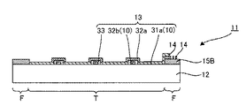
また、タッチパネルセンサにおいては、薄型化、軽量化の要請が高く、例えば、上述したタッチパネルセンサ部材と前面保護板とが一体で形成された構成が提案されている(例えば、特許文献2)。このようなタッチパネルセンサとしては、具体的には図16〜図18に示すように、絶縁基材12の一方の表面上に形成された透明電極層10を有するセンサ部13と、センサ部13の外側に形成された遮光性を有する加飾層15Bと、加飾層15B上に形成され透明電極層10と接続する配線層14と、配線層14と接続された外部接続端子17とを有し、センサ部13が設けられたタッチパネル領域Tと、配線層14、外部接続端子17、および加飾層15Bが設けられた額縁領域Fとを有する形態が提案されている。なお、図16は従来のタッチパネルセンサの一例を示す概略平面図であり、図17は図16のA−A線断面図であり、図18は図16のB−B線断面図である。また、センサ部13の構成については、後述する図1〜図4におけるセンサ部3で説明する内容と同様であるため、ここでの説明は省略する。
Moreover, in the touch panel sensor, there is a high demand for reduction in thickness and weight, and for example, a configuration in which the above-described touch panel sensor member and the front protective plate are integrally formed has been proposed (for example, Patent Document 2). Specifically, as such a touch panel sensor, as shown in FIGS. 16 to 18, a
ところで、近年、タッチパネル付表示装置においては、その意匠性についてもより重視されるようになってきており、タッチパネルセンサの額縁領域における意匠として、白色系の色の意匠が望まれる場合がある。 By the way, in recent years, in a display device with a touch panel, the design property is also more emphasized, and a white color design may be desired as a design in the frame region of the touch panel sensor.
しかしながら、額縁領域に形成される加飾層として白色系の色の加飾層を採用した場合、遮光性確保の観点から、黒色の加飾層に比べてその厚さを厚くする必要がある。そのため、上述したタッチパネルセンサ部材および前面保護板が一体に形成された形態を有するタッチパネルセンサにおいては、加飾層が形成された絶縁基材の表面上にスパッタ法等の蒸着法により透明電極層を形成した場合に、図19に示すように、加飾層15Wの段差による透明電極層10の断線が生じやすいという問題がある。なお、図19において説明していない符号については、上述した図17と同様とすることができるため、ここでの説明は省略する。
However, when a white-colored decorative layer is employed as the decorative layer formed in the frame region, it is necessary to increase the thickness of the decorative layer compared to the black decorative layer from the viewpoint of securing light shielding properties. Therefore, in the touch panel sensor having the form in which the touch panel sensor member and the front protective plate are integrally formed, the transparent electrode layer is formed on the surface of the insulating base material on which the decorative layer is formed by a vapor deposition method such as a sputtering method. When formed, as shown in FIG. 19, there is a problem that the
本発明は、上記実情に鑑みてなされたものであり、額縁領域に白色系の色の意匠を付与することができ、センサ部の透明電極層の断線を防止することが可能なタッチパネルセンサ、タッチパネル用部材および歩留まりの低下を防止して上記タッチパネルセンサを製造可能なタッチパネルセンサの製造方法を提供することを主目的とする。 The present invention has been made in view of the above circumstances, and can provide a design of a white color in a frame region and can prevent a transparent electrode layer of a sensor unit from being disconnected, and a touch panel sensor It is a main object of the present invention to provide a method for manufacturing a touch panel sensor capable of manufacturing the above-described touch panel sensor while preventing reduction of members and yield.
上記目的を達成するために、本発明は、絶縁基材と、上記絶縁基材の一方の表面上に形成された透明電極層を有するセンサ部と、上記絶縁基材の上記センサ部側の表面上に形成され上記透明電極層と接続された配線層とを有し、上記センサ部が設けられたタッチパネル領域と上記配線層が設けられた額縁領域とを有するタッチパネルセンサであって、上記額縁領域には、上記絶縁基材の上記配線層側とは反対側の表面上に、バインダー樹脂および白色顔料を含有し白色系の色を示す加飾層が形成されていることを特徴とするタッチパネルセンサを提供する。 In order to achieve the above object, the present invention provides an insulating substrate, a sensor unit having a transparent electrode layer formed on one surface of the insulating substrate, and a surface of the insulating substrate on the sensor unit side. A touch panel sensor having a wiring layer formed thereon and connected to the transparent electrode layer, the touch panel area having the sensor portion provided therein, and the frame area having the wiring layer provided therein, wherein the frame area The touch panel sensor is characterized in that a decorative layer containing a binder resin and a white pigment and showing a white color is formed on the surface of the insulating base opposite to the wiring layer side. I will provide a.
本発明によれば、上記額縁領域には、上記絶縁基材の上記配線層側とは反対側の表面上に、バインダー樹脂および白色顔料を含有し白色系の色を示す加飾層が形成されていることにより、額縁領域に白色系の色の意匠を付与することができ、センサ部の透明電極層の断線を防止することが可能なタッチパネルセンサとすることができる。 According to the present invention, in the frame region, a decorative layer containing a binder resin and a white pigment and showing a white color is formed on the surface of the insulating base opposite to the wiring layer side. Therefore, a design of a white color can be given to the frame region, and a touch panel sensor capable of preventing disconnection of the transparent electrode layer of the sensor unit can be obtained.
上記発明においては、上記額縁領域には、上記絶縁基材の上記配線層側の表面上に、バインダー樹脂および白色顔料を含有し白色系の色を示す配線層側加飾層が形成されていることが好ましい。加飾層および配線側加飾層を用いて額縁領域の遮光性、白色系の色の意匠を調整することができるため、加飾層の厚さを薄くすることができ、タッチパネルセンサをタッチパネル付表示装置に用いた場合の前面側の表面凹凸を小さくすることができる。 In the said invention, the said wiring area | region decoration layer which contains a binder resin and a white pigment and shows a white color is formed in the said frame area | region on the surface at the said wiring layer side of the said insulating base material. It is preferable. Because the decorative layer and the wiring side decorative layer can be used to adjust the light shielding property of the frame area and the design of the white color, the thickness of the decorative layer can be reduced, and the touch panel sensor is equipped with a touch panel. When used in a display device, surface irregularities on the front side can be reduced.
上記発明においては、上記加飾層および上記配線層の間に、遮光性を有する裏打ち層が形成されていることが好ましい。タッチパネルセンサにおける額縁領域の遮光性を良好なものとすることができ、加飾層を透過した光が配線層表面で反射して配線層が観察されることを好適に防止することができる。 In the said invention, it is preferable that the backing layer which has light-shielding property is formed between the said decoration layer and the said wiring layer. The light shielding property of the frame area in the touch panel sensor can be improved, and it is possible to suitably prevent the light transmitted through the decoration layer from being reflected on the surface of the wiring layer and observing the wiring layer.
本発明は、絶縁基材と、上記絶縁基材の一方の表面上に形成された透明電極層を有するセンサ形成部と、上記絶縁基材の上記センサ形成部側の表面上に形成され上記透明電極層と接続された配線層とを有し、上記センサ形成部が設けられたタッチパネル領域と上記配線層が設けられた額縁領域とを有するタッチパネルセンサ用部材であって、上記額縁領域には、上記絶縁基材の上記配線層側とは反対側の表面上に、バインダー樹脂および白色顔料を含有し白色系の色を示す加飾層が形成されていることを特徴とするタッチパネルセンサ用部材を提供する。 The present invention provides an insulating base material, a sensor forming portion having a transparent electrode layer formed on one surface of the insulating base material, and the transparent base material formed on the surface of the insulating base material on the sensor forming portion side. A touch panel sensor member having a wiring layer connected to the electrode layer, the touch panel region provided with the sensor forming portion, and the frame region provided with the wiring layer, wherein the frame region includes: A member for a touch panel sensor, wherein a decoration layer containing a binder resin and a white pigment and exhibiting a white color is formed on a surface of the insulating base opposite to the wiring layer side. provide.
本発明によれば、上記額縁領域には、上記絶縁基材の上記配線層側とは反対側の表面上に、バインダー樹脂および白色顔料を含有し白色系の色を示す加飾層が形成されていることにより、額縁領域に白色系の色の意匠を付与することができ、センサ形成部の透明電極層の断線を防止することが可能なタッチパネルセンサ用部材とすることができる。 According to the present invention, in the frame region, a decorative layer containing a binder resin and a white pigment and showing a white color is formed on the surface of the insulating base opposite to the wiring layer side. Therefore, a design of a white color can be imparted to the frame region, and a touch panel sensor member capable of preventing disconnection of the transparent electrode layer of the sensor forming portion can be obtained.
本発明は、絶縁基材の一方の表面上に透明電極層を有するセンサ部および上記透明電極層と接続された配線層を形成するセンサ部および配線層形成工程と、上記センサ部が設けられたタッチパネル領域と上記配線層が設けられた額縁領域とを有する上記絶縁基材の上記額縁領域における上記配線層側とは反対側の表面上に、バインダー樹脂および白色顔料を含有し白色系の色を示す加飾層を形成する加飾層形成工程とを有し、上記センサ部および配線層形成工程が、上記センサ部の上記透明電極層をフォトリソグラフィ法を用いて形成する工程であり、上記加飾層形成工程が、上記加飾層を印刷法を用いて形成する工程であることを特徴とするタッチパネルセンサの製造方法を提供する。 The present invention is provided with a sensor part having a transparent electrode layer on one surface of an insulating substrate, a sensor part for forming a wiring layer connected to the transparent electrode layer, a wiring layer forming step, and the sensor part. On the surface opposite to the wiring layer side in the frame region of the insulating base material having the touch panel region and the frame region provided with the wiring layer, a white color is contained on the surface opposite to the wiring layer side. A decorative layer forming step for forming the decorative layer to be shown, wherein the sensor portion and the wiring layer forming step are steps for forming the transparent electrode layer of the sensor portion using a photolithography method, A decoration layer formation process is a process of forming the above-mentioned decoration layer using a printing method, and provides a manufacturing method of a touch panel sensor characterized by things.
本発明によれば、上記センサ部および配線層形成工程ならびに加飾層形成工程を有することにより、絶縁基材の一方の表面上にフォトリソグラフィ法を用いてセンサ部の透明電極等を形成した後、上記絶縁基材の反対側の表面上に印刷法により加飾層を形成することができるため、歩留まりの低下を防止してタッチパネルセンサを製造することができる。 According to the present invention, after forming the sensor part and the wiring layer forming step and the decorative layer forming step, the transparent electrode of the sensor part is formed on one surface of the insulating base material using the photolithography method. Since the decorative layer can be formed on the surface on the opposite side of the insulating substrate by a printing method, it is possible to manufacture a touch panel sensor while preventing a decrease in yield.
本発明のタッチパネルセンサおよびタッチパネルセンサ用部材は、額縁領域に白色系の色の意匠を付与することができ、センサ部の透明電極層の断線を防止することができるといった作用効果を奏する。また、本発明のタッチパネルセンサの製造方法は、歩留まりの低下を防止して上記タッチパネルセンサを製造することができるといった作用効果を奏する。 The touch panel sensor and the member for a touch panel sensor of the present invention can provide a white-colored design to the frame region, and have an effect of preventing disconnection of the transparent electrode layer of the sensor unit. Moreover, the manufacturing method of the touch panel sensor of this invention has an effect that the said touch panel sensor can be manufactured preventing the fall of a yield.
以下、本発明のタッチパネルセンサ、タッチパネルセンサ用部材およびタッチパネルセンサの製造方法について説明する。 Hereinafter, the manufacturing method of the touch panel sensor, the member for touch panel sensors, and the touch panel sensor of the present invention will be described.
A.タッチパネルセンサ
本発明のタッチパネルセンサは、絶縁基材と、上記絶縁基材の一方の表面上に形成された透明電極層を有するセンサ部と、上記絶縁基材の上記センサ部側の表面上に形成され上記透明電極層と接続された配線層とを有し、上記センサ部が設けられたタッチパネル領域と上記配線層が設けられた額縁領域とを有するものであって、上記額縁領域には、上記絶縁基材の上記配線層側とは反対側の表面上に、バインダー樹脂および白色顔料を含有し白色系の色を示す加飾層が形成されていることを特徴とするものである。
A. Touch Panel Sensor The touch panel sensor of the present invention is formed on the surface of the insulating base, a sensor part having a transparent electrode layer formed on one surface of the insulating base, and the sensor part side surface of the insulating base. A wiring layer connected to the transparent electrode layer, and a touch panel region provided with the sensor unit and a frame region provided with the wiring layer, wherein the frame region includes A decorative layer containing a binder resin and a white pigment and showing a white color is formed on the surface of the insulating base opposite to the wiring layer side.
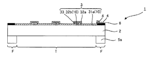
本発明のタッチパネルセンサについて図を用いて説明する。図1は本発明のタッチパネルセンサの一例を示す概略平面図であり、図2は図1のA−A線断面図であり、図3は図1のB−B線断面図であり、図4は図1のC−C線断面図である。
図1〜図4に示すように、本発明のタッチパネルセンサ1は、絶縁基材2と、絶縁基材2の一方の表面上に形成された透明電極層10を有するセンサ部3と、絶縁基材2のセンサ部3側の表面上に形成され透明電極層10と接続された配線層4と、を有する。また、タッチパネルセンサ1は、センサ部3が設けられたタッチパネル領域Tと配線層4が設けられた額縁領域Fとを有するものである。本発明においては、額縁領域Fには、絶縁基材2の配線層4側とは反対側の表面上に、バインダー樹脂および白色顔料を含有し白色系の色を示す加飾層5aが形成されていることを特徴とする。
The touch panel sensor of the present invention will be described with reference to the drawings. 1 is a schematic plan view showing an example of the touch panel sensor of the present invention, FIG. 2 is a cross-sectional view taken along line AA in FIG. 1, FIG. 3 is a cross-sectional view taken along line BB in FIG. FIG. 2 is a cross-sectional view taken along line CC in FIG. 1.
As shown in FIGS. 1 to 4, the
図1〜図4に示すセンサ部3は、絶縁基材2の同一面上に、互いに絶縁された第1電極31aおよび第2電極31bを有するセンサ電極と、第1電極31a同士を接続する第1導電部32aおよび第2電極31b同士を接続する第2導電部32bを有する導電部と、第1導電部32aおよび第2導電部32bの間に形成された層間絶縁層33とを有するものである。また、第1導電部32aおよび第2導電部32bはその一部が層間絶縁層33を介して平面視上重なるように形成されている。図1〜図4に示すセンサ部3は、投影型静電容量方式のタッチパネルセンサに対応する形態である。また、第1電極31a、第2電極31bおよび第2導電部32bが透明電極層10で形成されている。
また、配線層4は第1電極31aおよび第2電極31bとそれぞれ接続されて形成されており、配線層4は末端にて外部接続端子7と接続されて形成されている。また、図1〜3では、額縁領域Fには、絶縁基材2と配線層4との間に遮光性を有する裏打ち層6が形成されている例について示している。
なお、図1においては説明の容易の為、層間絶縁層、裏打ち層、加飾色層は省略されている。
The
The
In FIG. 1, the interlayer insulating layer, the backing layer, and the decorative color layer are omitted for ease of explanation.
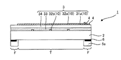
図5は本発明のタッチパネルセンサの他の例を示す概略断面図である。図5に示すように、額縁領域Fには、絶縁基材2の配線層4側とは反対側の表面上に、裏打ち層6が形成され、裏打ち層6上に加飾層5aが形成されていてもよい。なお、図5は図1のA−A線断面図に相当し、図5において説明していない符号については図2と同様とすることができるため、ここでの説明は省略する。
FIG. 5 is a schematic sectional view showing another example of the touch panel sensor of the present invention. As shown in FIG. 5, in the frame region F, a
図6は本発明のタッチパネルセンサの他の例を示す概略断面図である。図6に示すように、額縁領域Fには、絶縁基材2の配線層4側の表面上に、バインダー樹脂および白色顔料を含み白色系の色を示す配線層側加飾層5bが形成されていることが好ましい。なお、図6は図1のA−A線断面図に相当し、図6において説明していない符号については図2と同様とすることができるため、ここでの説明は省略する。
FIG. 6 is a schematic sectional view showing another example of the touch panel sensor of the present invention. As shown in FIG. 6, in the frame region F, a wiring layer side decorative layer 5 b including a binder resin and a white pigment and showing a white color is formed on the surface of the insulating
本発明のタッチパネルセンサは、通常、タッチパネル付表示装置に用いられるものであり、タッチパネル付表示装置における表示パネルの表示面側に配置される。また、本発明のタッチパネルセンサは、タッチパネルとしての機能と、タッチパネル付表示装置における前面保護板としての機能とを兼ね備えるものである。本発明のタッチパネルセンサは、通常、絶縁基材の配線層側の面を表示パネルの表示面と対向させて用いられ、絶縁基材の配線層側とは反対側の面を前面保護板として用いる。そこで、以下の説明においては「配線層側とは反対側」を「前面側」と称して説明する場合がある。 The touch panel sensor of the present invention is usually used for a display device with a touch panel, and is disposed on the display surface side of the display panel in the display device with a touch panel. The touch panel sensor of the present invention has both a function as a touch panel and a function as a front protective plate in a display device with a touch panel. The touch panel sensor of the present invention is usually used with the wiring layer side surface of the insulating base material facing the display surface of the display panel, and the surface opposite to the wiring layer side of the insulating base material is used as the front protective plate. . Therefore, in the following description, “the side opposite to the wiring layer side” may be referred to as “front side”.
本発明によれば、上記額縁領域には、上記絶縁基材の上記配線層側とは反対側の表面上に、バインダー樹脂および白色顔料を含有し白色系の色を示す加飾層が形成されていることにより、額縁領域に白色系の色の意匠を付与することができ、センサ部の透明電極層の断線を防止することが可能なタッチパネルセンサとすることができる。 According to the present invention, in the frame region, a decorative layer containing a binder resin and a white pigment and showing a white color is formed on the surface of the insulating base opposite to the wiring layer side. Therefore, a design of a white color can be given to the frame region, and a touch panel sensor capable of preventing disconnection of the transparent electrode layer of the sensor unit can be obtained.
より具体的には、本発明によれば、絶縁基材の前面側の表面上に上述の加飾層が形成されていることにより、例えば、図2および図3に示すように、センサ部3の透明電極層10と配線層4とを同一平面上に形成することができる。
また、絶縁基材の前面側の表面上に上述の加飾層が形成されていることにより、例えば、図5および図6に示すように、絶縁基材2の配線層4側の表面上に裏打ち層6や配線層側加飾層5bを形成する場合も、加飾層5aと裏打ち層6および配線層側加飾層5bとのそれぞれの厚さを調整することで、これらの層による段差を小さくして透明電極層10の断線を防止し、額縁領域Fに白色系の色の意匠を付与することができる。
よって、本発明によれば、絶縁基材の前面側の表面上に上述の加飾層が形成されていることにより、絶縁基材のセンサ部および配線層側に配置される構成による段差を小さいものとすることができるため、センサ部の透明電極層の断線を防止することができる。
More specifically, according to the present invention, the above-mentioned decorative layer is formed on the front surface of the insulating base material, for example, as shown in FIG. 2 and FIG. The
Moreover, since the above-mentioned decorating layer is formed on the front surface side of the insulating base material, for example, on the surface of the insulating
Therefore, according to the present invention, the above-described decorative layer is formed on the front surface of the insulating base material, thereby reducing the level difference due to the configuration arranged on the sensor portion and wiring layer side of the insulating base material. Since it can be set as a thing, disconnection of the transparent electrode layer of a sensor part can be prevented.
以下、本発明のタッチパネルセンサの詳細について説明する。 Hereinafter, details of the touch panel sensor of the present invention will be described.
1.タッチパネル領域および額縁領域
本発明のタッチパネルセンサは、タッチパネル領域と額縁領域とを有するものである。
タッチパネル領域は、センサ部が設けられた領域であり、タッチパネルセンサを用いたタッチパネル付表示装置の操作者によりタッチ操作が行われる領域である。また、タッチパネル領域は、本発明のタッチパネルセンサを用いたタッチパネル付表示装置において、表示パネルの表示領域に対応するように配置される領域である。
額縁領域は、少なくとも配線層および加飾層が設けられた領域であり、上述したタッチパネル領域の外側に位置する領域である。また、額縁領域においては、絶縁基材の前面側から配線層が視認されないように、配線層および加飾層を形成することにより、本発明のタッチパネルセンサを用いたタッチパネル付表示装置の外観が悪くなることを防止し、さらに、良好な意匠性を付与する領域である。
1. Touch Panel Area and Frame Area The touch panel sensor of the present invention has a touch panel area and a frame area.
The touch panel region is a region where a sensor unit is provided, and is a region where a touch operation is performed by an operator of a display device with a touch panel using a touch panel sensor. The touch panel area is an area arranged to correspond to the display area of the display panel in the display device with a touch panel using the touch panel sensor of the present invention.
The frame region is a region where at least a wiring layer and a decoration layer are provided, and is a region located outside the touch panel region described above. Further, in the frame region, the appearance of the display device with a touch panel using the touch panel sensor of the present invention is poor by forming the wiring layer and the decorative layer so that the wiring layer is not visually recognized from the front side of the insulating base material. It is an area | region which prevents becoming and also provides favorable design property.
本発明のタッチパネルセンサにおけるタッチパネル領域の大きさおよび位置については、タッチパネルセンサの用途に応じて適宜選択することができ特に限定されない。また、額縁領域の位置についてもタッチパネルセンサの用途等に応じて適宜選択することができ特に限定されないが、額縁領域は、通常、タッチパネル領域の外側を囲うように形成される。 About the magnitude | size and position of the touchscreen area | region in the touchscreen sensor of this invention, it can select suitably according to the use of a touchscreen sensor, and it does not specifically limit. Further, the position of the frame area can be appropriately selected according to the use of the touch panel sensor and the like, and is not particularly limited. However, the frame area is usually formed so as to surround the outside of the touch panel area.
2.タッチパネルセンサの各構成
本発明のタッチパネルセンサは、絶縁基材と、センサ部と、配線層と、加飾層とを有するものである。
2. Each structure of a touch panel sensor The touch panel sensor of this invention has an insulating base material, a sensor part, a wiring layer, and a decoration layer.
(1)加飾層
本発明に用いられる加飾層は、額縁領域に設けられるものであり、絶縁基材の配線層側とは反対側の表面上に形成されるものである。また、加飾層は、バインダー樹脂および白色顔料を含有し白色系の色を示すものである。
(1) Decoration layer The decoration layer used for this invention is provided in a frame area | region, and is formed on the surface on the opposite side to the wiring layer side of an insulating base material. The decorative layer contains a binder resin and a white pigment and exhibits a white color.
本発明において白色系の色とは、純粋な白色(純白)以外に、アイボリー色、ベージュ色、赤みの白である赤白色(薄いピンク色)、黄みの白である黄白色、青みの白である青白色、緑みの白である緑白色、紫みの白である紫白色、茶色みの白である茶白色、黒みの白である灰色(ライトグレー)、銀色みの白である銀白色、金色みの白である金白色などの、有彩色で白っぽい色、及び無彩色で白っぽい色、も含む。
こうした白色系の色は、各種表色系を用いて数値的に表現することができる。なかでも慣用的な表色系の1種であるマンセル表色系(JIS Z 8721)による場合、以下のように表現することができる。
マンセル表色系では、全ての色を、明度と、彩度と、色相の三属性によって表現する。この明度は、マンセル表色系では、最も明るい理想的な白を10とし、最も暗い理想的な黒を0とする。本発明においては、白色系の色の明度の下限としては、例えば8.0程度であり、なかでも8.0以上が好ましい。また、マンセル表色系では、彩度は、無彩色を0とし、色が濃くなるほど値か大きくなり、最大値は明度と色相によって変わるが最大で14である。本発明においては、白色系の色の彩度の上限としては、例えば2.0程度であり、2.0以下であることが好ましい。
本発明において白色系の色としては、マンセル表色系において、なかでも、明度が8.0以上で、かつ彩度が2.0以下の色であることが好ましい。色相については、特に制限はない。いかなる色味でも構わない。
In the present invention, the white color is not only pure white (pure white) but also ivory, beige, reddish white (light pink), yellowish white, yellowish white, and bluish white Blue white, greenish white, purple white, purple white, brown white, brown white, gray gray (light gray), silvery white silver Also included are chromatic and whitish colors, and achromatic and whitish colors, such as white and gold-white that is golden white.
Such white color can be expressed numerically using various color systems. In particular, in the case of the Munsell color system (JIS Z 8721) which is one kind of conventional color system, it can be expressed as follows.
In the Munsell color system, all colors are expressed by three attributes of lightness, saturation, and hue. In the Munsell color system, this brightness is 10 for the brightest ideal white and 0 for the darkest ideal black. In the present invention, the lower limit of the brightness of the white color is, for example, about 8.0, and more preferably 8.0 or more. In the Munsell color system, the saturation is 0 for an achromatic color, the value increases as the color becomes darker, and the maximum value varies with lightness and hue but is 14 at maximum. In the present invention, the upper limit of the saturation of the white color is, for example, about 2.0, and preferably 2.0 or less.
In the present invention, the white color is preferably a color having a lightness of 8.0 or more and a saturation of 2.0 or less in the Munsell color system. There is no particular limitation on the hue. Any color is acceptable.
より好ましい色について、マンセル表色系によって表現すれば、明度においては9.0以上の色の場合、彩度においては1.0以下の色の場合により効果的であり、さらに、明度が9.0以上で、かつ彩度が1.0以下の色の場合が、より効果的である。
マンセル表色系の上記三属性は、市販の分光測色計、分光光度計などによって測定することができる。
If more preferable colors are expressed by the Munsell color system, it is more effective when the lightness is 9.0 or higher, the saturation is 1.0 or lower, and the lightness is 9. The case where the color is 0 or more and the saturation is 1.0 or less is more effective.
The above three attributes of the Munsell color system can be measured with a commercially available spectrophotometer, spectrophotometer, or the like.
上記加飾層は、バインダー樹脂と白色顔料とを含有するものである。
上記バインダー樹脂としては、一般的なタッチパネルセンサの加飾層に用いられるものと同様とすることができる。例えば、上記加飾層をフォトリソグラフィ法で形成する場合は感光性樹脂を好適に用いることができ、印刷法で形成する場合は熱硬化性樹脂を好適に用いることができる。
The decorative layer contains a binder resin and a white pigment.
The binder resin can be the same as that used for a decorative layer of a general touch panel sensor. For example, when the decorative layer is formed by a photolithography method, a photosensitive resin can be suitably used, and when it is formed by a printing method, a thermosetting resin can be suitably used.
上記感光性樹脂としては、例えば、アクリル系樹脂、エポキシ系樹脂、ポリイミド系樹脂、ポリ桂皮酸ビニル系樹脂、環化ゴム等の反応性ビニル基などの光反応性基を有する感光性樹脂を1種以上を用いることができる。上記アクリル系樹脂では、例えば、アルカリ可溶性樹脂、多官能アクリレート系モノマー、光重合開始剤、その他添加剤などからなる感光性樹脂をバインダー樹脂の樹脂成分として用いることができる。 Examples of the photosensitive resin include a photosensitive resin having a photoreactive group such as an acrylic resin, an epoxy resin, a polyimide resin, a polyvinyl cinnamate resin, and a reactive vinyl group such as a cyclized rubber. More than seeds can be used. In the said acrylic resin, the photosensitive resin which consists of alkali-soluble resin, a polyfunctional acrylate monomer, a photoinitiator, another additive etc. can be used as a resin component of binder resin, for example.
上記アルカリ可溶性樹脂には、ベンジルメタクリレート−メタクリル酸共重合体などのメタクリル酸エステル共重合体、ビスフェノールフルオレン構造を有するエポキシアクリレートなどのカルド樹脂、などを1種以上用いることができる。
上記多官能アクリレート系モノマーには、例えば、トリメチロールプロパントリ(メタ)アクリレート、ペンタエリスリトールテトラ(メタ)アクリレート、ジペンタエリスリトールペンタ(メタ)アクリレート、ジペンタエリスリトールヘキサ(メタ)アクリレート、などを1種以上用いることができる。
なお、本発明において、(メタ)アクリレートとは、メタクリレート、又は、アクリレートのいずれかであることを意味する。
As the alkali-soluble resin, one or more kinds of methacrylic acid ester copolymers such as benzyl methacrylate-methacrylic acid copolymer, cardo resins such as epoxy acrylate having a bisphenolfluorene structure, and the like can be used.
Examples of the polyfunctional acrylate monomer include trimethylolpropane tri (meth) acrylate, pentaerythritol tetra (meth) acrylate, dipentaerythritol penta (meth) acrylate, dipentaerythritol hexa (meth) acrylate, and the like. The above can be used.
In the present invention, (meth) acrylate means either methacrylate or acrylate.
上記光重合開始剤には、アルキルフェノン系、オキシムエステル系、トリアジン系、チタネート系などを1種以上用いることができる。例えば、アルキルフェノン系では、2−メチル−1[4−(メチルチオ)フェニル]−2−モリフォリノプロパン−1−オン(イルガキュア(登録商標)907、BASFジャパン株式会社製)、2−ベンジル−2−ジメチルアミノ−1−(4−モノフォリオフェニル)ブタノン−1(イルガキュア(登録商標)369、BASFジャパン株式会社製)、オキシムエステル系では、1,2−オクタンジオン,1−[4−(フェニルチオ)−2−(O−ベンゾイルオキシム)](イルガキュア(登録商標)OXE01、BASFジャパン株式会社製)などを用いることができる。 As the photopolymerization initiator, one or more alkylphenone series, oxime ester series, triazine series, titanate series and the like can be used. For example, in the alkylphenone series, 2-methyl-1 [4- (methylthio) phenyl] -2-morpholinopropan-1-one (Irgacure (registered trademark) 907, manufactured by BASF Japan Ltd.), 2-benzyl- In 2-dimethylamino-1- (4-monofoliophenyl) butanone-1 (Irgacure (registered trademark) 369, manufactured by BASF Japan Ltd.), an oxime ester system, 1,2-octanedione, 1- [4- ( Phenylthio) -2- (O-benzoyloxime)] (Irgacure (registered trademark) OXE01, manufactured by BASF Japan Ltd.) and the like can be used.
上記熱硬化性樹脂としては、例えば、アクリル系樹脂、エポキシ系樹脂、ポリエステル系樹脂、ポリイミド系樹脂等を用いることができる。 As the thermosetting resin, for example, an acrylic resin, an epoxy resin, a polyester resin, a polyimide resin, or the like can be used.
また、白色顔料としては、例えば、酸化チタン、シリカ、タルク、カオリン、クレイ、硫酸バリウム、水酸化カルシウム、などを用いることができる。 Examples of white pigments that can be used include titanium oxide, silica, talc, kaolin, clay, barium sulfate, and calcium hydroxide.
上記加飾層は、顔料として上述した白色顔料のみを含有していてもよく、白色顔料および他の色の顔料を含有していてもよい。他の色の顔料としては、例えば、赤色顔料、黄色顔料、青色顔料、緑色顔料、紫色顔料、黒色顔料などを用いることができる。これらの顔料については一般的なものを用いることができる。 The decorative layer may contain only the white pigment described above as a pigment, or may contain a white pigment and a pigment of another color. As other color pigments, for example, red pigments, yellow pigments, blue pigments, green pigments, purple pigments, black pigments and the like can be used. A common thing can be used about these pigments.
上記加飾層は、上述したバインダー樹脂、白色顔料、他の色の顔料の他にも、例えば、光増感剤、分散剤、界面活性剤、安定剤、レベリング剤などの、公知の各種添加剤を含むことができる。 In addition to the binder resin, white pigment, and other color pigments described above, the decorative layer includes various known additions such as a photosensitizer, a dispersant, a surfactant, a stabilizer, and a leveling agent. An agent can be included.
上記加飾層に含有される顔料の含有量(白色顔料および他の顔料を含有する場合はその総量)としては、所望の遮光性および白色系の色を示し、所定の厚さで加飾層を形成することができれば特に限定されない。
例えば、加飾層のバインダー樹脂100質量部に対して、顔料が10質量部〜95質量部の範囲内、なかでも40質量部〜90質量部の範囲内、特に60質量部〜90質量部の範囲内であることが好ましい。
上記顔料の含有量が多いと加飾層を安定的に形成することが困難となる可能性があるからである。一方、上記顔料の含有量が少ないと加飾層の厚さが厚くなり、本発明のタッチパネルセンサの前面側の表面凹凸が大きくなることから、タッチパネルセンサの外観が悪くなる可能性や、タッチ操作の際にタッチパネル領域と額縁領域との境界で指等が引っ掛かりやすくなりタッチ操作がしにくくなる可能性があるからである。また、加飾層に破損等を生じやすくなる可能性があるからである。
The content of the pigment contained in the decorative layer (the total amount when a white pigment and other pigments are included) shows a desired light-shielding property and white color, and has a predetermined thickness. If it can form, it will not specifically limit.
For example, with respect to 100 parts by mass of the binder resin of the decorative layer, the pigment is in the range of 10 parts by mass to 95 parts by mass, especially in the range of 40 parts by mass to 90 parts by mass, particularly 60 parts by mass to 90 parts by mass. It is preferable to be within the range.
It is because it may become difficult to form a decoration layer stably when there is much content of the said pigment. On the other hand, if the content of the pigment is small, the thickness of the decorative layer is increased, and the surface unevenness on the front side of the touch panel sensor of the present invention is increased. This is because a finger or the like is likely to be caught at the boundary between the touch panel area and the frame area, and the touch operation may be difficult. Moreover, it is because it may become easy to produce a damage etc. in a decoration layer.
加飾層の形成方法としては、例えば、フォトリソグラフィ法、または、スクリーン印刷法、インクジェット法等の印刷法等を挙げることができる。
本発明においては、なかでも印刷法を用いることが好ましい。タッチパネルセンサの工程数を少なくすることができ、例えば、絶縁基材の一方の表面上にセンサ部および配線層を形成した後に、上記絶縁基材の反対側の表面上に加飾層を形成する場合、歩留まりの低下を防止することができるからである。
また、加飾層の形成方法においては、通常、上述した加飾層材料および溶剤を含む加飾層用組成物が調製される。上記加飾層用組成物に用いられる溶剤については、一般的なものとすることができ、例えば、プロピレングリコールモノメチルエーテル、プロピレングリコールモノメチルエーテルアセテート、エチルセロソルブ、3−メトキシブチルアセテート、等を1種以上用いることができる。
Examples of the method for forming the decorative layer include a photolithography method, a printing method such as a screen printing method, and an inkjet method.
In the present invention, it is particularly preferable to use a printing method. The number of steps of the touch panel sensor can be reduced. For example, after forming the sensor part and the wiring layer on one surface of the insulating base material, the decorative layer is formed on the surface on the opposite side of the insulating base material. This is because a decrease in yield can be prevented.
Moreover, in the formation method of a decoration layer, the composition for decoration layers containing the decoration layer material and solvent which were mentioned above is prepared normally. About the solvent used for the said composition for decorating layers, it can be made into a general thing, For example, propylene glycol monomethyl ether, propylene glycol monomethyl ether acetate, ethyl cellosolve, 3-methoxybutyl acetate, etc. are 1 type. The above can be used.
加飾層の厚さとしては、所定の遮光性および白色系の色を示すことができれば特に限定されないが、1μm〜50μmの範囲内、なかでも3μm〜30μmの範囲内、特に3μm〜20μmの範囲内であることが好ましい。
加飾層の厚さが厚いと本発明のタッチパネルセンサの前面側の表面凹凸が大きくなることから、タッチパネルセンサの外観が悪くなる可能性や、タッチ操作の際にタッチパネル領域と額縁領域との境界で指等が引っ掛かりやすくなりタッチ操作がしにくくなる可能性があるからである。また、加飾層が絶縁基材の表面から剥離する可能性があるからである。
また、加飾層の厚さが薄いと、絶縁基材の表面上に良好な加飾層を形成することが困難となる可能性があるからである。
The thickness of the decorative layer is not particularly limited as long as it can exhibit a predetermined light-shielding property and white color, but it is in the range of 1 μm to 50 μm, especially in the range of 3 μm to 30 μm, particularly in the range of 3 μm to 20 μm. It is preferable to be within.
If the thickness of the decoration layer is large, the surface unevenness on the front side of the touch panel sensor of the present invention becomes large, so that the appearance of the touch panel sensor may be deteriorated, or the boundary between the touch panel area and the frame area during touch operation This is because a finger or the like is likely to be caught and a touch operation may be difficult. Moreover, it is because a decorating layer may peel from the surface of an insulating base material.
Moreover, it is because it will become difficult to form a favorable decorating layer on the surface of an insulating base material when the thickness of a decorating layer is thin.
加飾層の幅については、本発明のタッチパネルセンサの用途に応じて適宜選択することができる。 About the width | variety of a decoration layer, it can select suitably according to the use of the touch panel sensor of this invention.
加飾層は、その一部に開口部を有していてもよい。上記開口部としては、例えば、本発明のタッチパネルセンサが用いられるタッチパネル付表示装置のカメラ部分に対応する開口部や、製品ロゴ等の文字、記号、標章等を挙げることができる。 The decorative layer may have an opening in a part thereof. Examples of the opening include an opening corresponding to a camera portion of a display device with a touch panel in which the touch panel sensor of the present invention is used, characters such as a product logo, a symbol, a mark, and the like.
(2)配線層
本発明における配線層は、絶縁基材のセンサ部側の表面上に形成され、センサ部の透明電極層と接続されるものである。また、配線層は、額縁領域に形成され、上述した加飾層と平面視上重なる位置に形成される。
(2) Wiring layer The wiring layer in this invention is formed on the surface by the side of the sensor part of an insulating base material, and is connected with the transparent electrode layer of a sensor part. The wiring layer is formed in the frame region and is formed at a position overlapping the above-described decoration layer in plan view.
配線層は、通常、金属材料を含有する。
上記金属材料としては、所望の導電性を有するものであれば特に限定されるものではなく、例えば、金属単体、金属の複合体、金属と金属化合物の複合体、金属合金等を挙げることができる。具体的には、金属単体としては、金、銀、銅、アルミニウム、白金、鉛、インジウム、パラジウム、ロジウム、ルテニウム、イリジウム、オスミウム、タングステン、ニッケル、タンタル、ビスマス、スズ、亜鉛、チタン、コバルト、鉄、モリブデンの単体等を例示することができる。金属の複合体としては、MAMと称されるモリブデン、アルミニウム、モリブデンの3層構造体等を挙げることができる。また、金属と金属化合物の複合体としては、酸化クロムおよびクロム形成体等を例示することができる。金属合金としては、銀合金や銅合金、APCと称される銀、パラジウム、銅の合金等を例示することができる。金属材料は単独で用いてもよく、2種類以上を組み合わせて用いてもよい。
The wiring layer usually contains a metal material.
The metal material is not particularly limited as long as it has desired conductivity, and examples thereof include a metal simple substance, a metal composite, a metal and metal compound composite, and a metal alloy. . Specifically, as a simple metal, gold, silver, copper, aluminum, platinum, lead, indium, palladium, rhodium, ruthenium, iridium, osmium, tungsten, nickel, tantalum, bismuth, tin, zinc, titanium, cobalt, Illustrative examples include iron and molybdenum alone. As the metal composite, a three-layer structure of molybdenum, aluminum, and molybdenum called MAM can be given. Examples of the complex of metal and metal compound include chromium oxide and a chromium-forming body. Examples of the metal alloy include a silver alloy, a copper alloy, and an alloy of silver, palladium, and copper called APC. A metal material may be used independently and may be used in combination of 2 or more types.
配線層の平面視形状については、透明電極層と接続させることができ、タッチパネル領域の外側に引き出して形成することができれば特に限定されず、一般的なタッチパネルセンサに用いられるものと同様とすることができるため、ここでの記載は省略する。
配線層の線幅としては、例えば10μm〜200μm程度とすることができる。
The shape of the wiring layer in plan view is not particularly limited as long as it can be connected to the transparent electrode layer and can be formed outside the touch panel region, and is the same as that used for a general touch panel sensor. The description here is omitted.
The line width of the wiring layer can be, for example, about 10 μm to 200 μm.
なお、配線層の形成方法については、高精細な配線層を形成可能な方法であれば特に限定されるものではなく、例えば、まず、金属材料からなる金属層を形成した後に、金属層上にレジスト層をパターン状に形成し、次いで、レジスト層をマスクとして金属層をエッチングする方法を挙げることができる。エッチング液としては、金属材料等に応じて適宜設定される。具体的には、金属層が銀やAPC等からなる場合には、燐硝酢酸等を用いることができる。金属層の形成方法としては、例えば、真空蒸着法、スパッタリング法、イオンプレーティング法、CVD法等のドライプロセスが挙げられる。また、配線層の形成方法としては、インクジェット法を用いることもできる。 The method for forming the wiring layer is not particularly limited as long as it is a method capable of forming a high-definition wiring layer. For example, after a metal layer made of a metal material is first formed, the wiring layer is formed on the metal layer. A method of forming a resist layer in a pattern and then etching the metal layer using the resist layer as a mask can be mentioned. The etching solution is appropriately set according to the metal material or the like. Specifically, when the metal layer is made of silver, APC, or the like, phosphorous nitric acid or the like can be used. Examples of the method for forming the metal layer include dry processes such as vacuum deposition, sputtering, ion plating, and CVD. In addition, as a method for forming the wiring layer, an inkjet method can also be used.
(3)センサ部
本発明に用いられるセンサ部は、絶縁基材の一方の表面上に形成された透明電極層を有するものである。また、センサ部は、タッチパネル領域に形成されるものである。センサ部の形態としては、本発明のタッチパネルセンサの動作原理により適宜選択することができ、特に限定されない。本発明のタッチパネルセンサにおいては、例えば、投影型静電容量方式を好適に用いることができる。以下、センサ部が投影型静電容量方式に対応する形態である場合を例に説明する。
(3) Sensor part The sensor part used for this invention has a transparent electrode layer formed on one surface of an insulating base material. The sensor unit is formed in the touch panel area. The form of the sensor unit can be appropriately selected according to the operation principle of the touch panel sensor of the present invention, and is not particularly limited. In the touch panel sensor of the present invention, for example, a projection capacitive method can be suitably used. Hereinafter, a case where the sensor unit is in a form corresponding to the projected capacitance method will be described as an example.
本発明に用いられるセンサ部としては、例えば、上述した図1〜4に示す形態、図7〜10に示す形態、図11〜図13に示す形態のものを挙げることができるがこれらに限定されない。 As a sensor part used for this invention, the thing shown in FIGS. 1-4 mentioned above, the form shown in FIGS. 7-10, the thing shown in FIGS. 11-13 can be mentioned, for example, However, It is not limited to these. .
ここで、図7〜図10に示すセンサ部3について説明する。このセンサ部3においては、絶縁基材2の片面であって層間絶縁層33を介して第1電極31aおよび第2電極31bが形成されている。この場合、図8および図9に示すように第1電極31aおよび第1導電部32a、ならびに第2電極31bおよび第2導電部32bが透明導電層10になり得る。
なお、図7は本発明のタッチパネルセンサの他の例を示す概略平面図であり、図8は図7のA−A線断面図であり、図9は図7のB−B線断面図であり、図10は図7のC−C線断面図である。なお、図7においては説明の容易の為、層間絶縁層、裏打ち層、加飾色層は省略されている。
Here, the
7 is a schematic plan view showing another example of the touch panel sensor of the present invention, FIG. 8 is a cross-sectional view taken along line AA in FIG. 7, and FIG. 9 is a cross-sectional view taken along line BB in FIG. FIG. 10 is a cross-sectional view taken along the line CC of FIG. In FIG. 7, the interlayer insulating layer, the backing layer, and the decorative color layer are omitted for ease of explanation.
また、図11〜図13に示すセンサ部3について説明する。このセンサ部3においては、第1電極31aおよび第1導電部32aが異なる絶縁基材(以下、センサ部用絶縁基材と称する)34上に形成され、第2電極31bおよび第2導電部32bが絶縁基材2上に形成されている。図11および図12に示すように第1電極31aおよび第1導電部32a、ならびに第2電極31bおよび第2導電部32bが透明導電層10になり得る。
なお、図11は図7のA−A線断面図、図12は図7のB−B線断面図、図13は図7のC−C線断面図に相当する。
Moreover, the
11 corresponds to a sectional view taken along line AA in FIG. 7, FIG. 12 corresponds to a sectional view taken along line BB in FIG. 7, and FIG. 13 corresponds to a sectional view taken along line CC in FIG.
本発明に用いられるセンサ部は、通常、センサ電極および導電部を少なくとも有する。以下、センサ部に用いられる構成について説明する。 The sensor part used in the present invention usually has at least a sensor electrode and a conductive part. Hereinafter, the configuration used for the sensor unit will be described.
(a)センサ電極
上記センサ部は、上記絶縁基材の一方の表面上に形成され、互いに絶縁された第1電極および第2電極を有するセンサ電極を有する。センサ電極は、タッチパネル領域内に形成され、接触位置を検出するために用いられるものである。
なお、第1電極および第2電極が互いに絶縁されているとは、両電極が電気的に接続されていないことをいう。
(A) Sensor electrode The sensor part has a sensor electrode which is formed on one surface of the insulating base and has a first electrode and a second electrode which are insulated from each other. The sensor electrode is formed in the touch panel area and is used for detecting the contact position.
Note that that the first electrode and the second electrode are insulated from each other means that the electrodes are not electrically connected.
センサ電極としては、通常、透明導電性材料を含む透明電極層が用いられる。
透明電極層に用いられる透明導電性材料としては、具体的には、インジウム錫酸化物(ITO)、酸化亜鉛、酸化インジウム、アンチモン添加酸化錫、フッ素添加酸化錫、アルミニウム添加酸化亜鉛、カリウム添加酸化亜鉛、シリコン添加酸化亜鉛や、酸化亜鉛−酸化錫系、酸化インジウム−酸化錫系、酸化亜鉛−酸化インジウム−酸化マグネシウム系などの金属酸化物や、これらの金属酸化物が2種以上複合された材料が挙げられる。
As the sensor electrode, a transparent electrode layer containing a transparent conductive material is usually used.
Specific examples of the transparent conductive material used for the transparent electrode layer include indium tin oxide (ITO), zinc oxide, indium oxide, antimony-added tin oxide, fluorine-added tin oxide, aluminum-added zinc oxide, and potassium-added oxide. Zinc, silicon-doped zinc oxide, metal oxides such as zinc oxide-tin oxide, indium oxide-tin oxide, zinc oxide-indium oxide-magnesium oxide, and two or more of these metal oxides were combined Materials.
センサ電極の平面視形状および平面視外形形状としては、特開2011−210176号公報、特開2010−238052号公報、特許第4610416号公報、特開2010-286886号公報、特開2004−192093号公報、特開2010−277392号公報、特開2011−129501号公報等に示されるような一般的なタッチパネルセンサにおけるセンサ電極と同様とすることができる。
センサ電極の平面視外形形状としては、より具体的には、平面視略正方形形状等の多角形状が挙げられる。また、センサ電極の平面視形状としては、連続的な面状であることが好ましい。
As the planar view shape and the planar view outer shape of the sensor electrode, JP 2011-210176 A, JP 2010-238052 A, JP 4610416 A, JP 2010-286886 A, and JP 2004-192093 A. It can be the same as that of a sensor electrode in a general touch panel sensor as disclosed in Japanese Patent Laid-Open No. 2010-277392, Japanese Patent Laid-Open No. 2011-129501, and the like.
More specifically, the outer shape of the sensor electrode in plan view includes a polygonal shape such as a substantially square shape in plan view. Moreover, as a planar view shape of a sensor electrode, it is preferable that it is a continuous planar shape.
絶縁基材に対する第1電極および第2電極の形成箇所としては、タッチパネル領域における絶縁基材の一方の表面上に第1電極および第2電極が、互いに絶縁されるように形成されていれば特に限定されるものではない。例えば、図4に示すように第1電極31aおよび第2電極31bが絶縁基材2の片面であって同一平面上に形成されていてもよく、図10に示すように第1電極31aおよび第2電極31bが絶縁基材2の片面に層間絶縁層33を介して形成されていてもよく、第1電極31aおよび第2電極31bのいずれか一方(図13では第2電極31b)が絶縁基材2の配線層4側の表面上に形成され、他方(図13では第1電極31a)がセンサ部用絶縁基材34上に形成されていてもよい。
As a formation location of the 1st electrode and 2nd electrode with respect to an insulation base material, if the 1st electrode and the 2nd electrode are formed so that it may be insulated from each other on one surface of the insulation base material in a touchscreen area | region, especially It is not limited. For example, as shown in FIG. 4, the
センサ電極の厚さとしては、一般的なタッチパネルセンサにおけるセンサ電極と同様とすることができる。 The thickness of the sensor electrode can be the same as that of a sensor electrode in a general touch panel sensor.
センサ電極の形成方法としては、高精細なセンサ電極を形成可能な方法であれば特に限定されるものではないが、フォトリソグラフィ法を用いた形成方法を好適に用いることができる。具体的には、上記透明導電材料を含む導電層を形成した後に、フォトリソグラフィ法により導電層上にレジスト層をパターン状に形成し、次いで、レジスト層をマスクとして導電層をエッチングする方法を挙げることができる。エッチング液としては、上記透明導電材料等に応じて適宜設定される。導電層の形成方法としては、例えば、真空蒸着法、スパッタリング法、イオンプレーティング法、CVD法等のドライプロセスが挙げられる。 A method for forming the sensor electrode is not particularly limited as long as it is a method capable of forming a high-definition sensor electrode, but a formation method using a photolithography method can be preferably used. Specifically, there is a method in which after forming a conductive layer containing the transparent conductive material, a resist layer is formed in a pattern on the conductive layer by photolithography, and then the conductive layer is etched using the resist layer as a mask. be able to. The etching solution is appropriately set according to the transparent conductive material and the like. Examples of the method for forming the conductive layer include dry processes such as vacuum deposition, sputtering, ion plating, and CVD.
(b)導電部
本発明のタッチパネルセンサは、第1電極同士を接続する第1導電部と第2電極同士を接続する第2導電部とを有する導電部を有する。通常、第1導電部および第2導電部はその一部が平面視上重なるように形成される。
(B) Conductive Part The touch panel sensor of the present invention has a conductive part having a first conductive part that connects the first electrodes and a second conductive part that connects the second electrodes. Usually, the first conductive portion and the second conductive portion are formed such that a part thereof overlaps in plan view.
導電部に用いられる導電材料としては、導電性を有するものであれば特に限定されるものではなく、上記センサ電極に用いられる材料と同様とすることができる。
導電部を構成する第1導電部および第2導電部の少なくともいずれかが上記透明導電層である場合には、透明導電材料から構成される透明電極層が用いられる。また、導電部には、非透明導電性材料を用いることもでき、具体的には、アルミニウム、モリブデン、銀、クロム等の金属およびその合金等を用いることができる。
The conductive material used for the conductive portion is not particularly limited as long as it has conductivity, and can be the same as the material used for the sensor electrode.
When at least one of the first conductive part and the second conductive part constituting the conductive part is the transparent conductive layer, a transparent electrode layer made of a transparent conductive material is used. In addition, a non-transparent conductive material can be used for the conductive portion, and specifically, a metal such as aluminum, molybdenum, silver, or chromium and an alloy thereof can be used.
導電部の平面視形状としては、タッチパネルセンサに一般的なものとすることができ、上記センサ電極と同様とすることができる。 The shape of the conductive portion in plan view can be common to touch panel sensors and can be the same as the sensor electrode.
また、導電部の平面視外形形状としては、タッチパネルセンサに一般的なものとすることができ、例えば、センサ電極の平面視外形形状より幅の狭いライン形状等が挙げられる。また、本発明においては、センサ電極および導電部の平面視外形形状が、ストライプ状になるように導電層を形成することもできる。 Further, the external shape of the conductive portion in plan view can be general to the touch panel sensor, and examples thereof include a line shape having a width narrower than that of the sensor electrode in plan view. In the present invention, the conductive layer may be formed so that the outer shape of the sensor electrode and the conductive portion in plan view is a stripe shape.
第1導電部および第2導電部の形成箇所としては、第1導電部および第2導電部によって第1電極間および第2電極間をそれぞれ安定的に接続でき、かつ、両者が絶縁されるように形成されていれば特に限定されるものではない。例えば、図10および図13に示すように、第1電極および第2電極が異なる平面または異なる部材上に形成される場合、第1導電部および第2導電部がそれぞれ第1電極および第2電極と同一平面上に形成される。また、図4に示すように第1電極および第2電極が絶縁基材の同一平面上に形成される場合には、第1導電部および第2導電部が層間絶縁層を介して形成される。 The first conductive portion and the second conductive portion are formed as the first conductive portion and the second conductive portion so that the first conductive portion and the second conductive portion can stably connect the first electrode and the second electrode, respectively, and are insulated from each other. If it is formed in, it will not specifically limit. For example, as shown in FIGS. 10 and 13, when the first electrode and the second electrode are formed on different planes or different members, the first conductive portion and the second conductive portion are respectively the first electrode and the second electrode. Are formed on the same plane. In addition, as shown in FIG. 4, when the first electrode and the second electrode are formed on the same plane of the insulating substrate, the first conductive portion and the second conductive portion are formed via the interlayer insulating layer. .
導電部の厚さとしては、一般的なタッチパネルセンサにおける導電部と同様とすることができる。 The thickness of the conductive part can be the same as the conductive part in a general touch panel sensor.
導電部の形成方法としては、上述したセンサ電極の形成方法と同様とすることができるため、ここでの説明は省略する。また、導電部が非透明導電材料を用いたものである場合は、インクジェット法を用いて形成することもできる。 The method for forming the conductive portion can be the same as the method for forming the sensor electrode described above, and a description thereof will be omitted here. Further, when the conductive portion is made of a non-transparent conductive material, it can be formed using an ink jet method.
(c)層間絶縁層
本発明に用いられるセンサ部は、必要に応じて層間絶縁層を有していてもよい。本発明における層間絶縁層は、第1電極および第2電極間あるいは第1導電部および第2導電部間の短絡を防止するために形成されるものである。
(C) Interlayer insulation layer The sensor part used for this invention may have an interlayer insulation layer as needed. The interlayer insulating layer in the present invention is formed to prevent a short circuit between the first electrode and the second electrode or between the first conductive portion and the second conductive portion.
層間絶縁層に用いられる絶縁材料としては、所望の絶縁性を有するものであれば特に限定されるものではなく、タッチパネルセンサに一般的に用いられるものを使用することができる。例えば、光透過性のアクリル樹脂、シロキサン樹脂等を挙げることができ、中でも感光性シロキサン樹脂を好ましく用いることができる。
また、後述するセンサ部用絶縁基材を有する場合は、層間絶縁層としては接着剤または粘着剤を用いて形成することもできる。接着剤または粘着剤としては一般的なタッチパネルセンサに用いられるものと同様とすることができる。
The insulating material used for the interlayer insulating layer is not particularly limited as long as it has a desired insulating property, and materials generally used for touch panel sensors can be used. For example, a light-transmitting acrylic resin, siloxane resin, and the like can be given, and among these, a photosensitive siloxane resin can be preferably used.
Moreover, when it has the insulating base material for sensor parts mentioned later, it can also form using an adhesive agent or an adhesive as an interlayer insulation layer. The adhesive or pressure-sensitive adhesive can be the same as that used for a general touch panel sensor.
層間絶縁層の形成箇所としては、タッチパネルセンサに一般的なものとすることができ、例えば図4に示すように第1電極31aおよび第2電極31bが絶縁基材2の同一平面上に形成されている場合には、図2および図3に示すように層間絶縁層33が第1導電部32aの下層にのみアイランド状に形成されるアイランドタイプや、図示はしないが、層間絶縁層が第1電極、第2電極および第2導電部上に形成され、第1導電部および第1電極が接続するためのコンタクトホールを有するように形成されているホールタイプが挙げられる。また、例えば、図10および図13に示すように、第1電極および第2電極が異なる平面または異なる部材上に形成される場合、図8、図9、図11および図12に示すように層間絶縁層33が第1電極31aおよび第1導電部32aと第2電極31bおよび第2導電部32bとの間に形成されていてもよい。
As a place where the interlayer insulating layer is formed, it can be a common one for touch panel sensors. For example, as shown in FIG. 4, the
層間絶縁層の厚さとしては、第1電極および第2電極間または第1導電部および第2導電部間の短絡を防止することができるものであれば特に限定されるものではなく、タッチパネルセンサに一般的なものとすることができる。例えば、層間絶縁層の厚さとしては、0.5μm〜3.0μmの範囲内とすることができる。 The thickness of the interlayer insulating layer is not particularly limited as long as it can prevent a short circuit between the first electrode and the second electrode or between the first conductive part and the second conductive part. Can be general. For example, the thickness of the interlayer insulating layer can be in the range of 0.5 μm to 3.0 μm.
層間絶縁層の形成方法としては、所定の位置に層間絶縁層を精度良く形成できるものであれば特に限定されるものではなく、フォトリソグラフィ法や、スクリーン印刷等の印刷法等を挙げることができる。また、絶縁性を示し、適当な光透過性かつ光学等方性を示すフィルムやシート等を所望の形状に加工し、層間絶縁層として積層させることも可能である。 The method for forming the interlayer insulating layer is not particularly limited as long as the interlayer insulating layer can be accurately formed at a predetermined position, and examples thereof include a photolithography method and a printing method such as screen printing. . It is also possible to process a film, a sheet, or the like that exhibits insulating properties and appropriate optical transparency and optical isotropy, and is laminated as an interlayer insulating layer.
(d)センサ部用絶縁基材
本発明に用いられるセンサ部においては、第1電極および第1導電部または第2電極および第2導電部のいずれか一方をセンサ部用絶縁基材上に形成してもよい。
(D) Insulating base material for sensor part In the sensor part used in the present invention, either the first electrode and the first conductive part or the second electrode and the second conductive part are formed on the insulating base material for the sensor part. May be.
センサ部用絶縁基材としては、センサ部用絶縁基材を構成する材料としては、絶縁性を有するものであれば特に限定されるものではない。上記センサ部用絶縁基材は、通常、透明性を有する。 The insulating base for the sensor part is not particularly limited as long as the material constituting the insulating base for the sensor part has an insulating property. The said insulating base material for sensor parts has transparency normally.
センサ部用絶縁基材を構成する材料としては、ガラス等の無機材料、ポリエチレンテレフタレート等のポリエステル系樹脂、アクリル系樹脂、ポリカーボネート等の樹脂材料等が挙げられる。ガラス等の無機材料を選択した場合には、タッチパネルセンサの強度を高め、また加熱温度などの製造条件の設定範囲を広くすることが可能になる。一方、樹脂材料を選択した場合には、タッチパネルセンサの軽量化が図られ、またタッチパネルセンサにフレキシブル性を付与することができる。 Examples of the material constituting the insulating base for the sensor unit include inorganic materials such as glass, polyester resins such as polyethylene terephthalate, resin materials such as acrylic resins and polycarbonate. When an inorganic material such as glass is selected, it is possible to increase the strength of the touch panel sensor and widen the setting range of manufacturing conditions such as heating temperature. On the other hand, when a resin material is selected, the touch panel sensor can be reduced in weight, and flexibility can be imparted to the touch panel sensor.
センサ部用絶縁基材の厚さとしては、センサ電極および導電部を形成することができれば特に限定されず、材料に応じて適宜選択される。例えば、センサ部用絶縁基材がガラス等の無機材料からなる場合には、0.3mm〜1.5mmの範囲内であることが好ましい。また、センサ部用絶縁基材が樹脂材料からなる場合には、可撓性を有するフィルム状であることが好ましく、具体的には50μm〜300μmの範囲内とすることが好ましい。
また、センサ部用絶縁基材の形態としては、可撓性を有するフィルム状であってもよく、板状であってもよい。
The thickness of the insulating base for the sensor part is not particularly limited as long as the sensor electrode and the conductive part can be formed, and is appropriately selected according to the material. For example, when the insulating base for the sensor unit is made of an inorganic material such as glass, it is preferably within a range of 0.3 mm to 1.5 mm. Moreover, when the insulating base material for sensor parts consists of a resin material, it is preferable that it is a flexible film form, and specifically, it is preferable to set it in the range of 50 micrometers-300 micrometers.
Moreover, as a form of the insulating base material for a sensor part, the film form which has flexibility may be sufficient, and plate shape may be sufficient.
(4)絶縁基材
本発明における絶縁基材は、上記のセンサ部、配線層、および加飾層等を支持するものである。また、本発明のタッチパネルセンサをタッチパネル付表示装置に用いる場合、絶縁基材は前面保護板としても用いられるものである。
本発明における絶縁基材は、通常、透明性を有する。
なお、本発明において、「透明」「透明性」という場合には、特段の断りがない限り、本発明のタッチパネルセンサが用いられたタッチパネル付表示装置の操作者が、操作面からの視認を妨げない程度の透明性をいう。したがって、無色透明および、視認性を妨げない程度の有色透明を含み、また厳密な透過率で規定されず、タッチパネルセンサの用途等に応じて適宜決定することができる。
(4) Insulating base material The insulating base material in this invention supports said sensor part, a wiring layer, a decoration layer, etc. Moreover, when using the touch panel sensor of this invention for a display apparatus with a touch panel, an insulating base material is used also as a front surface protection board.
The insulating base material in the present invention usually has transparency.
In the present invention, the terms “transparent” and “transparency” mean that an operator of a display device with a touch panel using the touch panel sensor of the present invention is not visually recognized from the operation surface unless otherwise specified. There is no transparency. Therefore, it includes colorless and transparent and colored transparency that does not impede visibility, is not defined by strict transmittance, and can be appropriately determined according to the use of the touch panel sensor.
絶縁基材を構成する材料としては、本発明のタッチパネルセンサを用いたタッチパネル付表示装置に対して、これらの表面を保護し得る機械強度を有するものであれば、特に限定されず、代表的にはガラス板を用いることができる。とくに、上記ガラス板として、化学強化ガラスはフロートガラスに比べて機械的強度に優れ、その分薄くできる点で好ましい。化学強化ガラスは、典型的には、ガラスの表面近傍について、ナトリウムをカリウムに代えるなどイオン種を一部交換することで、化学的な方法によって機械的物性を強化したガラスである。
絶縁基材には、樹脂を用いることも可能である。例えば、上記樹脂としては、アクリル系樹脂、ポリカーボネート系樹脂、シクロオレフィン系樹脂、ポリエステル系樹脂などを用いることができる。絶縁基材に樹脂を用いることで、軽量にできる上、可撓性を持たせることも可能となる。
The material constituting the insulating substrate is not particularly limited as long as it has mechanical strength capable of protecting these surfaces with respect to the display device with a touch panel using the touch panel sensor of the present invention, and representatively. A glass plate can be used. In particular, as the glass plate, chemically strengthened glass is preferable in that it has excellent mechanical strength compared to float glass and can be made thinner by that amount. Chemically tempered glass is typically glass whose mechanical properties have been reinforced by a chemical method by exchanging part of ionic species such as by replacing sodium with potassium in the vicinity of the surface of the glass.
It is also possible to use a resin for the insulating substrate. For example, as the resin, acrylic resin, polycarbonate resin, cycloolefin resin, polyester resin, or the like can be used. By using a resin for the insulating base material, the weight can be reduced and flexibility can be provided.
絶縁基材の厚さについては、本発明のタッチパネルセンサの用途に応じて適宜選択することができる。 About the thickness of an insulation base material, it can select suitably according to the use of the touch panel sensor of this invention.
(5)その他の構成
本発明のタッチパネルセンサは、上述した絶縁基材、加飾層、センサ部、および加飾層を有していれば特に限定されず、必要に応じて他の構成を適宜選択して用いることができる。
(5) Other configurations The touch panel sensor of the present invention is not particularly limited as long as it has the insulating base, the decorative layer, the sensor unit, and the decorative layer described above, and other configurations are appropriately configured as necessary. It can be selected and used.
(a)配線層側加飾層
本発明のタッチパネルセンサにおいては、上記額縁領域には、上記絶縁基材の上記配線層側の表面上にバインダー樹脂および白色顔料を含み白色系の色を示す配線層側加飾層が形成されていることが好ましい。加飾層および配線側加飾層を用いて額縁領域の遮光性、白色系の色の意匠性を調整することができるため、加飾層の厚さを薄くすることができ、タッチパネルセンサにおける前面側の表面凹凸を小さくすることができる。
(A) Wiring layer side decoration layer In the touch panel sensor of the present invention, the frame region includes a binder resin and a white pigment on the surface of the insulating base on the wiring layer side, and shows a white color. It is preferable that the layer side decoration layer is formed. The decorative layer and the wiring side decorative layer can be used to adjust the light shielding property of the frame area and the design of the white color, so the thickness of the decorative layer can be reduced, and the front surface of the touch panel sensor The surface unevenness on the side can be reduced.
配線層側加飾層の厚さとしては、透明電極層の断線を防止することができれば特に限定されないが、50μm以下、なかでも1μm〜30μmの範囲内、特に1μm〜10μmの範囲内であることが好ましい。
配線層側加飾層の厚さが厚いと透明電極層の断線を十分に防止することが困難となる可能性があるからであり、配線層側加飾層の厚さが薄いと配線層側加飾層を形成した場合も、加飾層の厚さを薄くすることが困難となる可能性があるからである。また、配線層側加飾層を良好に形成することが困難となる可能性や、配線層側加飾層上に形成される配線層を良好に形成することが困難となる可能性があるからである。
The thickness of the decorative layer on the wiring layer side is not particularly limited as long as it can prevent the disconnection of the transparent electrode layer, but it is 50 μm or less, especially within the range of 1 μm to 30 μm, particularly within the range of 1 μm to 10 μm. Is preferred.
This is because if the wiring layer side decoration layer is thick, it may be difficult to sufficiently prevent disconnection of the transparent electrode layer. If the wiring layer side decoration layer is thin, the wiring layer side This is because even when the decorative layer is formed, it may be difficult to reduce the thickness of the decorative layer. In addition, it may be difficult to form the wiring layer side decorative layer satisfactorily or it may be difficult to form the wiring layer formed on the wiring layer side decorative layer. It is.
配線層側加飾層に用いられるバインダー樹脂、白色顔料、その他の材料等、および配線層側加飾層の形成方法については、上述した「(1)加飾層」の項で説明した内容と同様とすることができるため、ここでの説明は省略する。
本発明においては、上述した加飾層と配線層側加飾層との色みを異ならせ、加飾層と配線層側加飾層とを重ね合わせることにより、タッチパネルセンサの額縁領域に意匠性を付与することもできる。
The binder resin, white pigment, other materials, and the like used for the wiring layer side decorative layer, and the method for forming the wiring layer side decorative layer are the same as those described in the above-mentioned section “(1) Decorative layer”. Since it can be the same, description here is abbreviate | omitted.
In the present invention, the decorative layer and the wiring layer side decorative layer described above are made different in color, and the decorative layer and the wiring layer side decorative layer are overlapped to thereby provide a design property in the frame area of the touch panel sensor. Can also be given.
配線層側加飾層の幅としては、本発明のタッチパネルセンサの用途に応じて適宜選択することができ特に限定されない。例えば、配線層側加飾層の幅が上述した加飾層の幅と同等の幅で形成されていてもよく、加飾層の幅よりも小さい幅で形成されていてもよい。本発明においては、なかでも、配線層側加飾層の幅が加飾層の幅よりも小さい幅で形成されていることが好ましい。加飾層が形成されている領域内に配線層側加飾層を形成しやすくなることから、本発明のタッチパネルセンサを前面側から観察した場合に、配線層側加飾層が観察されることによる外観の低下を防止することができるからである。加飾層の幅に対する配線層側加飾層の幅の比率については、後述する加飾層の幅に対する裏打ち層の幅の比率と同様とすることができるため、ここでの説明は省略する。 The width of the wiring layer side decorative layer can be appropriately selected according to the application of the touch panel sensor of the present invention, and is not particularly limited. For example, the width of the wiring layer side decoration layer may be formed with a width equal to the width of the decoration layer described above, or may be formed with a width smaller than the width of the decoration layer. Especially in this invention, it is preferable that the width | variety of the wiring layer side decoration layer is formed in the width | variety smaller than the width | variety of a decoration layer. Since it becomes easy to form the wiring layer side decoration layer in the region where the decoration layer is formed, the wiring layer side decoration layer is observed when the touch panel sensor of the present invention is observed from the front side. This is because it is possible to prevent deterioration of the appearance due to the above. Since the ratio of the width of the wiring layer side decoration layer to the width of the decoration layer can be the same as the ratio of the width of the backing layer to the width of the decoration layer described later, description thereof is omitted here.
(b)裏打ち層
本発明のタッチパネルセンサにおいては、上記額縁領域には、上記加飾層および上記配線層の間に遮光性を有する裏打ち層が形成されていることが好ましい。加飾層の配線層側に裏打ち層が形成されていることにより、タッチパネルセンサにおける額縁領域の遮光性を良好なものとすることができ、加飾層を透過した光が配線層表面で反射して配線層が観察されることを好適に防止することができる。
(B) Backing layer In the touch panel sensor of the present invention, it is preferable that a light-blocking backing layer is formed between the decorative layer and the wiring layer in the frame region. Since the backing layer is formed on the wiring layer side of the decorative layer, the light shielding property of the frame area in the touch panel sensor can be improved, and the light transmitted through the decorative layer is reflected on the surface of the wiring layer. Thus, the observation of the wiring layer can be suitably prevented.
裏打ち層の形成位置としては、額縁領域における加飾層および上記配線層の間であって本発明のタッチパネルセンサを前面側から見た場合に加飾層の意匠性を低下させない位置であれば特に限定されない。例えば、図2等に示すように、額縁領域Fにおける絶縁基材2の配線層4側の表面上に裏打ち層6および配線層4の順で形成されていてもよく、図5に示すように、額縁領域Fにおける絶縁基材2の前面側の表面上に裏打ち層6および加飾層5aの順で形成されていてもよい。また、図6に示すように、額縁領域Fにおける絶縁基材2の配線層4側の表面上に配線層側加飾層5bが形成されている場合は、配線層側加飾層5b上に裏打ち層6および配線層4の順に形成される。
As the position where the backing layer is formed, it is between the decorative layer in the frame region and the wiring layer, and particularly if it is a position that does not deteriorate the design of the decorative layer when the touch panel sensor of the present invention is viewed from the front side. It is not limited. For example, as shown in FIG. 2 and the like, the
裏打ち層の材料としては、遮光性を有するものであれば特に限定されないが、バインダー樹脂および遮光材料を含有するものであることが好ましい。裏打ち層を絶縁性とすることができるため、裏打ち層上に配線層を形成しやすいからである。また、本発明においては、加飾層が絶縁基材の前面側の表面上に形成されていることにより、裏打ち層をフォトリソグラフィ法を用いて形成する場合に、良好に製版して形成することができる。 The material for the backing layer is not particularly limited as long as it has a light shielding property, but preferably contains a binder resin and a light shielding material. This is because the backing layer can be made insulative, so that a wiring layer can be easily formed on the backing layer. In the present invention, the decorative layer is formed on the surface on the front side of the insulating base material, so that when the backing layer is formed using a photolithographic method, the plate is formed well and formed. Can do.
ここで、白色系の色の加飾層を絶縁基材の配線層側の表面上に形成した場合において、上記加飾層上に裏打ち層をフォトリソグラフィ法を用いて形成した場合は、裏打ち層を良好に製版することができず、図20に示すように、加飾層15W上に裏打ち層16が形成されるだけでなく、加飾層15Wの近傍の絶縁基材12上にも裏打ち層16の製版残り18が形成される場合がある。この理由については明らかではないが以下のように推量される。すなわち、絶縁基材から加飾層表面までの段差が大きいことにより、バインダー樹脂および遮光材料を含む塗工液を塗布した場合、加飾層表面に形成される塗布膜の厚さよりも加飾層の近傍の絶縁基材の表面上に形成される塗布膜の厚さの方が厚くなる。そのため、現像時において、加飾層の近傍の絶縁基材の表面上に形成された塗布膜が十分に現像されないことが推量される。
なお、図20は従来のタッチパネルセンサの他の例を示す概略断面図であり、図16に示すタッチパネルセンサのA−A線断面図に相当し、説明していない符号等については図13と同様とすることができる。
Here, when the white-colored decorative layer is formed on the surface of the insulating base on the wiring layer side, when the backing layer is formed on the decorative layer using a photolithography method, the backing layer As shown in FIG. 20, not only the
FIG. 20 is a schematic cross-sectional view showing another example of the conventional touch panel sensor, which corresponds to the cross-sectional view taken along the line AA of the touch panel sensor shown in FIG. It can be.
これに対して、本発明においては、加飾層が絶縁基材の前面側の表面上に形成されていることから、例えば、絶縁基材の表面上に直に裏打ち層を形成することができる。また、配線層側加飾層上に裏打ち層を形成する場合も、配線層側加飾層の厚さを調整することにより、上記製版残りの少ないものとすることができる。 On the other hand, in the present invention, since the decorative layer is formed on the front surface of the insulating substrate, for example, the backing layer can be formed directly on the surface of the insulating substrate. . Moreover, also when forming a lining layer on a wiring layer side decorating layer, the said plate-making remainder can be made small by adjusting the thickness of a wiring layer side decorating layer.
裏打ち層に用いられる具体的なバインダー樹脂については上述した加飾層の項で説明した内容と同様とすることができる。また、遮光材料としては、例えば黒鉛、チタンブラック等の黒色顔料を挙げることができる。 The specific binder resin used for the backing layer can be the same as that described in the above-mentioned decoration layer. Examples of the light shielding material include black pigments such as graphite and titanium black.
裏打ち層の幅としては、本発明のタッチパネルセンサを前面側から観察した場合に、加飾層と平面視上重なるように裏打ち層を形成することができる幅であればよく、例えば、裏打ち層の幅が上述した加飾層の幅と同等の幅であってもよく、加飾層の幅よりも小さい幅であってもよい。本発明においては、なかでも、裏打ち層の幅が加飾層の幅よりも小さい幅であることが好ましい。本発明のタッチパネルセンサを用いたタッチパネル付表示装置を前面側の斜め方向から観察した場合に、裏打ち層が観察されることを防止することができるからである。
加飾層の幅に対する裏打ち層の幅の比率としては、例えば、80%〜100%の範囲内、なかでも90%〜100%の範囲内、特に95%〜100%の範囲内であることが好ましい。
The width of the backing layer may be any width that allows the backing layer to be formed so as to overlap the decorative layer in plan view when the touch panel sensor of the present invention is observed from the front side. The width may be equal to the width of the decorative layer described above, or may be smaller than the width of the decorative layer. In the present invention, it is particularly preferable that the width of the backing layer is smaller than the width of the decorative layer. This is because when the display device with a touch panel using the touch panel sensor of the present invention is observed from an oblique direction on the front side, it is possible to prevent the backing layer from being observed.
The ratio of the width of the backing layer to the width of the decorative layer is, for example, in the range of 80% to 100%, in particular in the range of 90% to 100%, particularly in the range of 95% to 100%. preferable.
具体的な裏打ち層の幅については、タッチパネルセンサの用途に応じて適宜選択することができる。 The specific width of the backing layer can be appropriately selected according to the use of the touch panel sensor.
裏打ち層の形成方法としては、上述した加飾層の項で説明した方法と同様とすることができるため、ここでの説明は省略する。 Since the method for forming the backing layer can be the same as the method described in the above-mentioned decoration layer, the description thereof is omitted here.
(c)保護層
本発明における保護層は、絶縁基材の表面上に形成されたセンサ部、および配線層を覆うように形成されるものである。また、上記保護層は、タッチパネルセンサのセンサ部および配線層側の最表面に形成されていることが好ましい。
保護層としては、絶縁性を有していれば特に限定されるものではないが、透明性を有することが好ましい。このような絶縁性および透明性を有する保護層としては、例えば、アクリル樹脂等の有機材料や酸化ケイ素等の無機材料等からなるものを挙げることができる。
(C) Protective layer The protective layer in this invention is formed so that the sensor part and wiring layer which were formed on the surface of the insulating base material may be covered. Moreover, it is preferable that the said protective layer is formed in the outermost surface at the side of the sensor part and wiring layer of a touchscreen sensor.
The protective layer is not particularly limited as long as it has insulating properties, but preferably has transparency. Examples of such a protective layer having insulation and transparency include those made of an organic material such as an acrylic resin or an inorganic material such as silicon oxide.
(d)外部接続端子
本発明のタッチパネルセンサは、上記配線層に接続された外部接続端子を有する。外部接続端子は、フレキシブルプリント配線板等との接続に用いられるものである。
(D) External connection terminal The touch panel sensor of the present invention has an external connection terminal connected to the wiring layer. The external connection terminal is used for connection with a flexible printed wiring board or the like.
外部接続端子の形成箇所および外部接続端子の材料については、上記配線層と同様とすることができる。 The formation location of the external connection terminal and the material of the external connection terminal can be the same as those of the wiring layer.
外部接続端子の端子幅、厚さおよび平面視形状や、外部接続端子部内における外部接続端子間の間隔については、一般的なタッチパネルセンサと同様とすることができる。具体的には、特開2011−210176号公報に記載されるものと同様とすることができる。 The terminal width and thickness of the external connection terminals, the shape in plan view, and the interval between the external connection terminals in the external connection terminal portion can be the same as those of a general touch panel sensor. Specifically, it can be the same as that described in JP2011-210176A.
3.タッチパネルセンサの製造方法
本発明のタッチパネルセンサの製造方法としては、上述した構成を有するタッチパネルセンサを製造することができる方法であれば特に限定されない。例えば、後述する「C.タッチパネルセンサの製造方法」の項で説明する方法を好適に用いることができる。
3. Method for Manufacturing Touch Panel Sensor The method for manufacturing the touch panel sensor of the present invention is not particularly limited as long as it is a method capable of manufacturing the touch panel sensor having the above-described configuration. For example, the method described in the section “C. Manufacturing method of touch panel sensor” described later can be suitably used.
B.タッチパネルセンサ用部材
本発明のタッチパネルセンサ用部材は、絶縁基材と、上記絶縁基材の一方の表面上に形成された透明電極層を有するセンサ形成部と、上記絶縁基材の上記センサ形成部側の表面上に形成され上記透明電極層と接続された配線層とを有し、上記センサ形成部が設けられたタッチパネル領域と上記配線層が設けられた額縁領域とを有するものであって、上記額縁領域には、上記絶縁基材の上記配線層側とは反対側の表面上に、バインダー樹脂および白色顔料を含有し白色系の色を示す加飾層が形成されていることを特徴とするものである。
B. Touch Panel Sensor Member The touch panel sensor member of the present invention includes an insulating base material, a sensor forming portion having a transparent electrode layer formed on one surface of the insulating base material, and the sensor forming portion of the insulating base material. A wiring layer formed on the surface on the side and connected to the transparent electrode layer, having a touch panel region provided with the sensor forming portion and a frame region provided with the wiring layer, In the frame region, a decorative layer containing a binder resin and a white pigment and showing a white color is formed on the surface of the insulating base opposite to the wiring layer side. To do.
本発明のタッチパネルセンサ用部材について図を用いて説明する。図14(a)は本発明のタッチパネルセンサ用部材の一例を示す概略平面図であり、図14(b)は図14(a)のA−A線断面図であり、図14(c)は図14(a)のB−B線断面図である。
図14(a)〜(c)に示すように、本発明のタッチパネルセンサ用部材20は、絶縁基材2と、絶縁基材2の一方の表面上に形成された透明電極層10を有するセンサ形成部23と、絶縁基材2のセンサ形成部23側の表面上に形成され透明電極層10と接続された配線層4と、を有する。また、タッチパネルセンサ1は、センサ形成部23が設けられたタッチパネル領域Tと配線層4が設けられた額縁領域Fとを有するものである。本発明においては、額縁領域Fには、絶縁基材2の配線層4側とは反対側の表面上に、バインダー樹脂および白色顔料を含有し白色系の色を示す加飾層5aが形成されていることを特徴とする。図14(a)〜(c)に示すタッチパネルセンサ用部材20は、例えば、上述した図11〜図13に示されるタッチパネルセンサ10を形成する際に用いられる。また、図14(a)〜(c)に示すセンサ形成部23は、図11〜図13に示されるタッチパネルセンサ10におけるセンサ部3の一部を構成するものであり、具体的には、第2電極31bおよび第2電極31b同士を接続する第2電極部32bであり、これらは透明電極層10で形成されている。また、配線層4は、第2電極31bと接続されて形成され、末端にて外部接続端子7と接続されて形成されている。
なお、図14(a)においては説明の容易の為、加飾層および裏打ち層は省略されている。
The member for touch panel sensors of this invention is demonstrated using figures. FIG. 14A is a schematic plan view showing an example of a member for a touch panel sensor of the present invention, FIG. 14B is a cross-sectional view taken along line AA in FIG. 14A, and FIG. It is the BB sectional view taken on the line of Fig.14 (a).
As shown in FIGS. 14A to 14C, the touch
In FIG. 14A, the decorative layer and the backing layer are omitted for ease of explanation.
本発明によれば、上記額縁領域には、上記絶縁基材の上記配線層側とは反対側の表面上に、バインダー樹脂および白色顔料を含有し白色系の色を示す加飾層が形成されていることにより、額縁領域に白色系の色の意匠を付与することができ、センサ形成部の透明電極層の断線を防止することが可能なタッチパネルセンサ用部材とすることができる。 According to the present invention, in the frame region, a decorative layer containing a binder resin and a white pigment and showing a white color is formed on the surface of the insulating base opposite to the wiring layer side. Therefore, a design of a white color can be imparted to the frame region, and a touch panel sensor member capable of preventing disconnection of the transparent electrode layer of the sensor forming portion can be obtained.
以下、本発明のタッチパネルセンサ用部材の詳細について説明する。 Hereinafter, the detail of the member for touch panel sensors of this invention is demonstrated.
1.タッチパネル領域および額縁領域
本発明のタッチパネルセンサ用部材は、タッチパネル領域と額縁領域とを有するものである。
タッチパネル領域は、センサ形成部が設けられた領域であり、タッチパネルセンサのセンサ部が設けられる領域である。また、タッチパネル領域について上記の点以外および額縁領域については、上述した「A.タッチパネルセンサ」の項で説明した内容と同様とすることができるため、ここでの説明は省略する。
1. Touch Panel Region and Frame Region The touch panel sensor member of the present invention has a touch panel region and a frame region.
The touch panel region is a region where a sensor forming unit is provided, and is a region where a sensor unit of the touch panel sensor is provided. The touch panel area other than the above points and the frame area can be the same as the contents described in the above-mentioned section “A. Touch panel sensor”, and thus the description thereof is omitted here.
2.タッチパネルセンサの各構成
本発明のタッチパネルセンサは、絶縁基材と、センサ形成部と、配線層と、加飾層とを有するものである。
なお、絶縁基材、配線層、加飾層については、「A.タッチパネルセンサ」の項で説明した内容と同様とすることができるため、ここでの説明は省略する。
2. Each structure of a touch panel sensor The touch panel sensor of this invention has an insulating base material, a sensor formation part, a wiring layer, and a decoration layer.
In addition, about an insulating base material, a wiring layer, and a decoration layer, since it can be made to be the same as that of the content demonstrated by the term of "A. touch panel sensor", description here is abbreviate | omitted.
本発明に用いられるセンサ形成部は、絶縁基材の一方の表面上に形成された透明電極層を有するものである。また、センサ形成部は、タッチパネル領域に形成されるものである。また、センサ形成部は、上述したセンサ部の一部を構成するものである。
センサ部の形態としては、センサ部の形態に応じて適宜選択される。投影型静電容量方式の場合、センサ形成部は、通常、センサ部のセンサ電極における第1電極および第1導電部または第2電極および第2導電部のいずれかを有する。
センサ形成部が用いられるセンサ電極および導電部については上述した「A.タッチパネルセンサ」の項で説明した内容と同様とすることができるため、ここでの説明は省略する。
The sensor formation part used for this invention has a transparent electrode layer formed on one surface of an insulating base material. The sensor forming part is formed in the touch panel area. Further, the sensor forming unit constitutes a part of the above-described sensor unit.
The form of the sensor unit is appropriately selected according to the form of the sensor unit. In the case of the projected capacitive method, the sensor forming unit usually has either the first electrode and the first conductive unit or the second electrode and the second conductive unit in the sensor electrode of the sensor unit.
Since the sensor electrode and the conductive part in which the sensor forming unit is used can be the same as the contents described in the above-mentioned section “A. Touch panel sensor”, description thereof is omitted here.
本発明のタッチパネルセンサ用部材においては、さらに、配線層側加飾層、裏打ち層および外部接続端子を有していてもよい。これらの構成については、上述した「A.タッチパネルセンサ」の項で説明した内容と同様とすることができるため、ここでの説明は省略する。 The touch panel sensor member of the present invention may further include a wiring layer side decorative layer, a backing layer, and an external connection terminal. About these structures, since it can be made to be the same as that of the content demonstrated by the term of the "A. touch panel sensor" mentioned above, description here is abbreviate | omitted.
3.タッチパネルセンサ用部材の製造方法
本発明のタッチパネルセンサ用部材の製造方法については特に限定されず、例えば、絶縁基材の一方の表面上に透明電極層を有するセンサ形成部および上記透明電極層と接続された配線層を形成するセンサ形成部および配線層形成工程と、上記センサ形成部が設けられたタッチパネル領域と上記配線層が設けられた額縁領域とを有する上記絶縁基材の上記額縁領域における上記配線層側とは反対側の表面上に、バインダー樹脂および白色顔料を含有し白色系の色を示す加飾層を形成する加飾層形成工程とを有し、上記センサ形成部および配線層形成工程が、上記センサ形成部の上記透明電極層をフォトリソグラフィ法を用いて形成する工程であり、上記加飾層形成工程が、上記加飾層を印刷法を用いて形成する工程であることを特徴とする製造方法を挙げることができる。
なお、詳細については、後述する「C.タッチパネルセンサの製造方法」の項で説明するため、ここでの説明は省略する。
3. The manufacturing method of the member for touch panel sensors is not specifically limited about the manufacturing method of the member for touch panel sensors of this invention, For example, it connects with the sensor formation part which has a transparent electrode layer on one surface of an insulating base material, and the said transparent electrode layer The above-described frame region of the insulating base material having the sensor forming unit and the wiring layer forming step for forming the wiring layer, the touch panel region where the sensor forming unit is provided, and the frame region where the wiring layer is provided A decorative layer forming step of forming a decorative layer containing a binder resin and a white pigment and showing a white color on the surface opposite to the wiring layer side, and forming the sensor forming portion and the wiring layer. The step is a step of forming the transparent electrode layer of the sensor forming portion using a photolithography method, and the decorative layer forming step is configured to form the decorative layer using a printing method. The manufacturing method characterized by being the process to form can be mentioned.
The details will be described in the section “C. Method for manufacturing touch panel sensor” described later, and thus the description thereof is omitted here.
C.タッチパネルセンサの製造方法
本発明のタッチパネルセンサの製造方法は、絶縁基材の一方の表面上に透明電極層を有するセンサ部および上記透明電極層と接続された配線層を形成するセンサ部および配線層形成工程と、上記センサ部が設けられたタッチパネル領域と上記配線層が設けられた額縁領域とを有する上記絶縁基材の上記額縁領域における上記配線層側とは反対側の表面上に、バインダー樹脂および白色顔料を含有し白色系の色を示す加飾層を形成する加飾層形成工程とを有し、上記センサ部および配線層形成工程が、上記センサ部の上記透明電極層をフォトリソグラフィ法を用いて形成する工程であり、上記加飾層形成工程が、上記加飾層を印刷法を用いて形成する工程であることを特徴とする製造方法である。
C. Method for Manufacturing Touch Panel Sensor The method for manufacturing a touch panel sensor according to the present invention includes a sensor unit having a transparent electrode layer on one surface of an insulating substrate, and a sensor unit and a wiring layer that form a wiring layer connected to the transparent electrode layer. A binder resin on a surface opposite to the wiring layer side in the frame region of the insulating base material, which includes a forming step, a touch panel region in which the sensor unit is provided, and a frame region in which the wiring layer is provided. And a decorative layer forming step of forming a decorative layer containing a white pigment and exhibiting a white color, wherein the sensor part and the wiring layer forming step are photolithography methods for the transparent electrode layer of the sensor part. The decorative layer forming step is a step of forming the decorative layer using a printing method.
本発明のタッチパネルセンサの製造方法について図を用いて説明する。図15(a)〜(g)は本発明のタッチパネルセンサの製造方法の一例を示す工程図である。本発明のタッチパネルセンサの製造方法においては、まず、図示はしないが、絶縁基材を準備する。次に、図15(a)に示すように、絶縁基材2の一方の表面上にフォトリソグラフィ法または印刷法を用いて配線層4を形成する。次に、図15(b)に示すように、配線層4が形成された絶縁基材2上にスパッタ法等の物理的蒸着法により透明導電材料で構成される導電層31を形成する。次に、図15(c)に示すように、導電層31が形成された絶縁基材2上にレジストを塗布してレジスト層20を形成した後、フォトマスクMを用いて露光光Lを照射し、現像することにより、図15(d)に示す所定のパターン状にレジスト層20を形成する。次に、パターン状のレジスト層20が形成された導電層31の露出部分をエッチングする。この際、エッチングの条件としては、導電層31を除去することができ、配線層4については除去されない条件とする。その後、レジスト層20を剥離することにより、図15(e)に示すように、透明電極層10で構成された第1電極31a、第2電極(図示なし)および第2導電部32bを形成する。次に、第2導電部32b上に印刷法等により層間絶縁層33を形成し、次いで、第1電極31aおよび層間絶縁層33上に第1導電部32aを形成する。以上の工程により、図15(f)に示すように、絶縁基材2の一方の表面上にセンサ部3および配線層4を形成する(センサ部および配線層形成工程)。
次に、図15(g)に示すように、センサ部3が設けられたタッチパネル領域Tと配線層4が設けられた額縁領域Fとを有する絶縁基材2の額縁領域Tにおける配線層4側とは反対側の表面上に、バインダー樹脂および白色顔料を含有するインクを用いて、スクリーン印刷法等の印刷法を用いて白色系の色を示す加飾層5aを形成する(加飾層形成工程)。本発明においては、加飾層5aの形成前に、絶縁基材2の額縁領域Tにおける配線層4側とは反対側の表面上に、バインダー樹脂および遮光材料を含有するインクを用いて印刷法等により、裏打ち層6を形成してもよい。
以上の工程により、図15(g)に示すようにタッチパネルセンサ1を製造することができる。
The manufacturing method of the touch panel sensor of this invention is demonstrated using figures. 15A to 15G are process diagrams illustrating an example of a method for manufacturing a touch panel sensor of the present invention. In the method for manufacturing a touch panel sensor of the present invention, first, although not shown, an insulating base material is prepared. Next, as shown in FIG. 15A, the
Next, as shown in FIG. 15G, the
Through the above steps, the
本発明によれば、上記センサ部および配線層形成工程ならびに加飾層形成工程を有することにより、フォトリソグラフィ法を用いてセンサ部の透明電極層を絶縁基材の一方の表面上に形成した後、上記絶縁基材の反対側の表面上に工程数の少ない印刷法を用いて加飾層を形成することができるため、タッチパネルセンサの製造過程におけるセンサ部および配線層等への損傷、汚損等を少なくすることができ、歩留まりの低下を防止してタッチパネルセンサを製造することができる。 According to the present invention, after having formed the transparent electrode layer of the sensor unit on one surface of the insulating base material by using the photolithography method by having the sensor unit and wiring layer forming step and the decorative layer forming step. Since the decoration layer can be formed on the surface on the opposite side of the insulating base material using a printing method with a small number of processes, the sensor part and the wiring layer, etc. in the manufacturing process of the touch panel sensor are damaged, stained, etc. The touch panel sensor can be manufactured while preventing a decrease in yield.
以下、本発明のタッチパネルセンサの製造方法の詳細について説明する。 Hereinafter, the detail of the manufacturing method of the touch panel sensor of this invention is demonstrated.
1.センサ部および配線層形成工程
本発明におけるセンサ部および配線層形成工程は、絶縁基材の一方の表面上に透明電極層を有するセンサ部および上記透明電極層に接続された配線層を形成する工程である。また、センサ部および配線層形成工程は、上記センサ部の上記透明電極層をフォトリソグラフィ法を用いて形成する工程である。
1. Sensor part and wiring layer formation process The sensor part and wiring layer formation process in this invention are the process of forming the wiring part connected to the sensor part which has a transparent electrode layer on one surface of an insulating base material, and the said transparent electrode layer It is. The sensor part and wiring layer forming step is a step of forming the transparent electrode layer of the sensor part using a photolithography method.
フォトリソグラフィ法を用いた透明電極層の形成方法については、上述した「A.タッチパネルセンサ」の項で説明した内容と同様とすることができるため、ここでの説明は省略する。 The method for forming the transparent electrode layer using the photolithography method can be the same as the content described in the above-mentioned section “A. Touch panel sensor”, and thus the description thereof is omitted here.
本発明においては、フォトリソグラフィ法を用いてセンサ部の透明電極層を形成することができれば良く、センサ部における他の構成および配線層については、フォトリソグラフィ法を用いて形成してもよく、印刷法を用いて形成してもよい。 In the present invention, it is only necessary that the transparent electrode layer of the sensor unit can be formed by using a photolithography method, and other configurations and wiring layers in the sensor unit may be formed by using a photolithography method and printing. You may form using a method.
センサ部に形成される構成、その材料、および形成方法について、ならびに配線層の材料および形成方法については、上述した「A.タッチパネルセンサ」の項で説明した内容と同様とすることができるため、ここでの説明は省略する。 About the structure formed in the sensor part, its material, and the forming method, and the material and the forming method of the wiring layer can be the same as the contents described in the above-mentioned section “A. Touch panel sensor”. The description here is omitted.
2.加飾層形成工程
本発明における加飾層形成工程は、上記センサ部が設けられたタッチパネル領域と上記配線層が設けられた額縁領域とを有する上記絶縁基材の上記額縁領域における上記配線層側とは反対側の表面上に、バインダー樹脂および白色顔料を含有し白色系の色を示す加飾層を形成する工程である。また、上記加飾層形成工程は、上記加飾層を印刷法を用いて形成する工程である。
2. Decoration layer formation process The decoration layer formation process in this invention is the said wiring layer side in the said frame area | region of the said insulating base material which has the touchscreen area | region in which the said sensor part was provided, and the frame area | region in which the said wiring layer was provided. Is a step of forming a decorative layer containing a binder resin and a white pigment and showing a white color on the opposite surface. Moreover, the said decoration layer formation process is a process of forming the said decoration layer using a printing method.
本工程は、通常、絶縁基材のセンサ部および配線部側に配置される構成を全て形成した後に、行なわれることが好ましい。絶縁基材のセンサ部および配線部側に配置される構成に対する損傷、汚損等をより少なくすることができるからである。 In general, this step is preferably performed after all the components arranged on the sensor portion and wiring portion side of the insulating base are formed. This is because damage, contamination, and the like with respect to the configuration arranged on the sensor portion and the wiring portion side of the insulating base material can be further reduced.
本工程により形成される加飾層およびその材料、形成方法については、上述した「A.タッチパネルセンサ」の項で説明した内容と同様であるため、ここでの説明は省略する。 About the decoration layer formed by this process, its material, and the formation method, since it is the same as that of the content demonstrated by the term of the "A. touch panel sensor" mentioned above, description here is abbreviate | omitted.
3.その他の構成
本発明のタッチパネルセンサの製造方法は、上述したセンサ部および配線部形成工程と、加飾層形成工程とを有していれば特に限定されず、必要に応じて他の工程を適宜選択して追加することができる。
このような工程としては、例えば、絶縁基材の配線層側の表面上に配線層側加飾層を形成する工程、絶縁基材の配線層側または前面側の表面上に裏打ち層を形成する工程、絶縁基材の配線層側の表面上に配線層と接続された外部接続端子を形成する工程、絶縁基材の一方の表面上に形成されたセンサ部および配線層を覆うように保護層を形成する工程等を挙げることができる。これらの工程は、加飾層形成工程前に行なうことが好ましい。また、配線層側加飾層、裏打ち層および外部接続端子について、これらの材料ならびに形成方法については、上述した「A.タッチパネルセンサ」の項で説明した内容と同様とすることができるため、ここでの説明は省略する。
3. Other Configurations The method for manufacturing a touch panel sensor of the present invention is not particularly limited as long as it includes the above-described sensor part and wiring part forming process and a decorative layer forming process, and other processes are appropriately performed as necessary. You can select and add.
As such a process, for example, a step of forming a wiring layer side decorative layer on the surface of the insulating base material on the wiring layer side, a backing layer is formed on the surface of the insulating base material on the wiring layer side or the front surface side. A step of forming an external connection terminal connected to the wiring layer on the surface of the insulating substrate on the wiring layer side, a protective layer so as to cover the sensor portion and the wiring layer formed on one surface of the insulating substrate The process etc. which form can be mentioned. These steps are preferably performed before the decorative layer forming step. In addition, for the wiring layer side decorative layer, the backing layer, and the external connection terminal, these materials and the forming method can be the same as the contents described in the above-mentioned section “A. Touch panel sensor”. The description in is omitted.
なお、本発明は、上記実施形態に限定されるものではない。上記実施形態は、例示であり、本発明の特許請求の範囲に記載された技術的思想と実質的に同一な構成を有し、同様な作用効果を奏するものは、いかなるものであっても本発明の技術的範囲に包含される。 The present invention is not limited to the above embodiment. The above-described embodiment is an exemplification, and the present invention has substantially the same configuration as the technical idea described in the claims of the present invention, and any device that exhibits the same function and effect is the present invention. It is included in the technical scope of the invention.
以下、実施例および比較例を挙げて本発明のタッチパネルセンサの詳細について説明する。 Hereinafter, the touch panel sensor of the present invention will be described in detail with reference to examples and comparative examples.
[実施例1]
(裏打ち層の作製)
厚さ0.5mmの透明ガラス基材(日本板硝子社製青板強化ガラス)を用いた。透明ガラス基材の表面上に遮光性粒子を含有する遮光性感光性樹脂組成物をスピンコート法により塗布して裏打ち層形成用層を形成した。フォトリソグラフィ法により、裏打ち層形成用層をパターン露光し、現像することにより厚さ3μm、幅9.5mmの額縁状の裏打ち層を形成した。
[Example 1]
(Production of backing layer)
A transparent glass base material (blue plate tempered glass manufactured by Nippon Sheet Glass Co., Ltd.) having a thickness of 0.5 mm was used. A light-shielding photosensitive resin composition containing light-shielding particles was applied on the surface of the transparent glass substrate by a spin coating method to form a backing layer forming layer. A pattern-like backing layer having a thickness of 3 μm and a width of 9.5 mm was formed by pattern exposure of the backing layer forming layer by photolithography and development.
(センサ部および配線部の作製)
上記透明ガラス基材の裏打ち層が形成された表面上にスパッタリング法により厚さ30nmのITO膜を成膜した。そして、ITO膜上にポジ型感光樹脂(レジスト)を用いて感光膜を形成し、フォトリソグラフィ法によってITO膜をパターニングし、第1電極、第2電極および第2導電部を形成した。
次に、上記各構成を形成した透明ガラス基材上全面に透明性感光性樹脂組成物をスピンコート法で塗布して層間絶縁層形成用層を形成し、続いてフォトリソグラフィ法により、一部露出面を残して第1電極、第2電極および第2導電部を覆うように層間絶縁層形成用層をパターニングし、層間絶縁層を形成した。
次に、銀、パラジウムおよび銅を含むAPC合金を用いて、スパッタリング法により厚さ100nmの金属膜を形成した。次に金属膜上にポジ型感光樹脂(レジスト)を塗布し、フォトリソグラフィ法によってパターニングした。ここで、レジストのパターンは、第1電極間を接続させるためのブリッジ部(第1導電部)、配線層、および外部接続端子に対応するパターンを有するものとした。また、配線層および外部接続端子に対応するパターンは、裏打ち層上に形成され、裏打ち層で配線層が第1電極および第2電極と接続するものとした。その後、燐硝酢酸系のエッチング液を用いて、エッチングした。
最後に、上記パターニングを行った透明ガラス基材上全面に、透明性感光性樹脂組成物をスピンコート法にて塗布して保護層形成用層をさらに形成し、続いてフォトリソグラフィ法により、接続端子パターンを残して第1電極、第1導電部(ブリッジ部)、第2電極、第2導電部、および配線層を覆うように保護層形成用層をパターニングし、保護層を形成した。
以上の工程によりセンサ部および配線層等を得た。
(Manufacture of sensor part and wiring part)
An ITO film having a thickness of 30 nm was formed on the surface of the transparent glass substrate on which the backing layer was formed by sputtering. Then, a positive photosensitive resin (resist) was formed on the ITO film, and the ITO film was patterned by a photolithography method, thereby forming the first electrode, the second electrode, and the second conductive portion.
Next, a transparent photosensitive resin composition is applied to the entire surface of the transparent glass substrate having the above-described structures by a spin coating method to form an interlayer insulating layer forming layer, followed by photolithography. The interlayer insulating layer forming layer was patterned to leave the exposed surface and cover the first electrode, the second electrode, and the second conductive portion, thereby forming an interlayer insulating layer.
Next, a 100 nm-thick metal film was formed by sputtering using an APC alloy containing silver, palladium, and copper. Next, a positive photosensitive resin (resist) was applied onto the metal film and patterned by photolithography. Here, the resist pattern has a pattern corresponding to a bridge portion (first conductive portion) for connecting the first electrodes, a wiring layer, and an external connection terminal. The pattern corresponding to the wiring layer and the external connection terminal is formed on the backing layer, and the wiring layer is connected to the first electrode and the second electrode in the backing layer. After that, etching was performed using a phosphorous acetate acetic acid-based etching solution.
Finally, a transparent photosensitive resin composition is applied on the entire surface of the transparent glass substrate subjected to the above patterning by a spin coating method to further form a protective layer forming layer, and subsequently connected by a photolithography method. The protective layer forming layer was patterned so as to cover the first electrode, the first conductive portion (bridge portion), the second electrode, the second conductive portion, and the wiring layer, leaving the terminal pattern, thereby forming a protective layer.
The sensor part, the wiring layer, etc. were obtained by the above process.
(加飾層の作製)
上記透明ガラス基材のセンサ部が形成された表面とは反対側の表面上に、白色顔料を有する白色硬化性樹脂組成物を用いてスクリーン印刷法により、厚さ40μmの加飾層を形成した。加飾層は、上述の裏打ち層と平面視上重なる額縁状に形成し、その幅は、10mmとした。
以上の工程により、タッチパネルセンサを得た。
(Preparation of decoration layer)
A decorative layer having a thickness of 40 μm was formed by screen printing using a white curable resin composition having a white pigment on the surface opposite to the surface on which the sensor portion of the transparent glass substrate was formed. . The decorative layer was formed in a frame shape overlapping the above-described backing layer in plan view, and the width was 10 mm.
The touch panel sensor was obtained by the above process.
[実施例2]
まず、透明ガラス基材の表面上に、実施例1と同様の方法によりセンサ部および配線層等を形成した。
次に、透明ガラス基材のセンサ部等が形成された表面とは反対側の表面上に実施例1と同様の方法により裏打ち層を形成した。
次に、透明基材の裏打ち層が形成された表面上に裏打ち層が平面視上重なるようにして実施例1と同様の方法により加飾層を形成した。
[Example 2]
First, a sensor part, a wiring layer, and the like were formed on the surface of the transparent glass substrate by the same method as in Example 1.
Next, a backing layer was formed by the same method as in Example 1 on the surface opposite to the surface on which the sensor portion of the transparent glass substrate was formed.
Next, a decorative layer was formed by the same method as in Example 1 so that the backing layer overlapped on the surface of the transparent base material on which the backing layer was formed.
[実施例3]
透明ガラス基材の表面上に、白色顔料を有する白色硬化性樹脂組成物を用いてスクリーン印刷法により、厚さ30μm、幅10mmの額縁状の配線層側加飾層を形成した。
次に、透明ガラス基材の配線層側加飾層が形成された表面上に遮光性粒子を含有する遮光性感光性樹脂組成物をスピンコート法により塗布して裏打ち層形成用層を形成した。フォトリソグラフィ法により、裏打ち層形成用層をパターン露光し、現像することにより配線層側加飾層と平面視上重なるように、厚さ3μm、幅10mmの額縁状の裏打ち層を形成した。
次に、透明ガラス基材の裏打ち層が形成された表面上に実施例1と同様にして、センサ部および配線層を形成した。
上記透明ガラス基材のセンサ部が形成された表面とは反対側の表面上に、実施例1と同様の方法により厚さ10μmの加飾層を形成した。また、実施例3においては、加飾層の幅を裏打ち層の幅と同様とした。
以上の工程により、タッチパネルセンサを得た。
[Example 3]
On the surface of the transparent glass substrate, a frame-shaped wiring layer side decorative layer having a thickness of 30 μm and a width of 10 mm was formed by a screen printing method using a white curable resin composition having a white pigment.
Next, a backing layer forming layer was formed by applying a light-shielding photosensitive resin composition containing light-shielding particles on the surface of the transparent glass substrate on which the wiring layer side decorative layer was formed by spin coating. . A pattern-like backing layer having a thickness of 3 μm and a width of 10 mm was formed by pattern exposure of the backing layer forming layer by photolithography and development to overlap the wiring layer side decorative layer in plan view.
Next, a sensor part and a wiring layer were formed in the same manner as in Example 1 on the surface on which the backing layer of the transparent glass substrate was formed.
A decorative layer having a thickness of 10 μm was formed on the surface opposite to the surface on which the sensor portion of the transparent glass substrate was formed, by the same method as in Example 1. In Example 3, the width of the decorative layer was the same as the width of the backing layer.
The touch panel sensor was obtained by the above process.
[比較例]
透明ガラス基材の表面上に、白色顔料を有する白色硬化性樹脂組成物を用いてスクリーン印刷法により、厚さ40μm、幅10mmの額縁状の加飾層を形成した。
次に、加飾層上に実施例1と同様にして裏打ち層を形成した。
次に、透明ガラス基材の裏打ち層が形成された表面上に実施例1と同様にして、センサ部および配線層を形成した。
以上の工程により、タッチパネルセンサを得た。
[Comparative example]
A frame-shaped decorative layer having a thickness of 40 μm and a width of 10 mm was formed on the surface of the transparent glass substrate by a screen printing method using a white curable resin composition having a white pigment.
Next, a backing layer was formed in the same manner as in Example 1 on the decorative layer.
Next, a sensor part and a wiring layer were formed in the same manner as in Example 1 on the surface on which the backing layer of the transparent glass substrate was formed.
The touch panel sensor was obtained by the above process.
[評価]
(断線の有無)
額縁領域における透明電極層の断線の有無について調べた。実施例1〜3のタッチパネルセンサにおいては断線が生じていなかった。一方、実施例1〜3に比べて加飾層によるタッチパネルセンサ表面の段差が大きい比較例のタッチパネルセンサにおいては断線が生じていた。結果を表1に示す。
[Evaluation]
(With or without disconnection)
The presence or absence of disconnection of the transparent electrode layer in the frame region was examined. No disconnection occurred in the touch panel sensors of Examples 1 to 3. On the other hand, in the touch panel sensor of the comparative example in which the level difference on the surface of the touch panel sensor due to the decorative layer is larger than in Examples 1 to 3, disconnection occurred. The results are shown in Table 1.
(裏打ち層の製版不良)
実施例3および比較例のタッチパネルセンサにおける裏打ち層の製版不良について調べた。実施例3のタッチパネルは、配線層側加飾層近傍の透明ガラス基材上には裏打ち層の製版残りがないものとすることができた。一方、実施例3に比べて加飾層によるタッチパネルセンサ表面の段差が大きい比較例のタッチパネルセンサにおいては、加飾層近傍の透明ガラス基材上に裏打ち層の製版残りが存在するものとなった。また、実施例1および実施例2のタッチパネルセンサにおいては、透明ガラス基材上に裏打ち層を直接形成することができることから、裏打ち層の製版残りがないものとすることができた。結果を表1に示す。
(The plate making of the backing layer is defective)
The plate making failure of the backing layer in the touch panel sensor of Example 3 and Comparative Example was examined. The touch panel of Example 3 could be such that there was no plate-making residue of the backing layer on the transparent glass substrate near the wiring layer side decorative layer. On the other hand, in the touch panel sensor of the comparative example having a large step on the surface of the touch panel sensor due to the decorative layer as compared with Example 3, the plate-making residue of the backing layer exists on the transparent glass substrate in the vicinity of the decorative layer. . Moreover, in the touch panel sensor of Example 1 and Example 2, since the backing layer can be directly formed on the transparent glass substrate, it was possible to make no remaining plate making of the backing layer. The results are shown in Table 1.

1、11 … タッチパネルセンサ
2、12 … 絶縁基材
3、13 … センサ部
4、14 … 配線層
5a、15B、15W … 加飾層
5b … 配線層側加飾層
6、16 … 裏打ち層
10 … 透明電極層
DESCRIPTION OF
Claims (4)
前記絶縁基材の一方の表面上に形成された透明電極層を有するセンサ部と、
前記絶縁基材の前記センサ部側の表面上に形成され前記透明電極層と接続された配線層とを有し、
前記センサ部が設けられたタッチパネル領域と前記配線層が設けられた額縁領域とを有するタッチパネルセンサであって、
前記額縁領域には、前記絶縁基材の前記配線層側とは反対側の表面上に、バインダー樹脂および白色顔料を含有し白色系の色を示す加飾層が形成されており、
前記額縁領域には、前記加飾層および前記配線層の間に、遮光性を有する裏打ち層が形成されており、
前記裏打ち層の幅が前記加飾層の幅より小さい幅であることを特徴とするタッチパネルセンサ。 An insulating substrate;
A sensor unit having a transparent electrode layer formed on one surface of the insulating substrate;
A wiring layer formed on the surface of the insulating base on the sensor part side and connected to the transparent electrode layer;
A touch panel sensor having a touch panel region provided with the sensor unit and a frame region provided with the wiring layer,
In the frame region, on the surface opposite to the wiring layer side of the insulating base, a decorative layer containing a binder resin and a white pigment and showing a white color is formed ,
In the frame area, a backing layer having a light shielding property is formed between the decorative layer and the wiring layer,
The touch panel sensor, wherein the backing layer has a width smaller than that of the decorative layer .
前記絶縁基材の一方の表面上に形成された透明電極層を有するセンサ形成部と、
前記絶縁基材の前記センサ形成部側の表面上に形成され前記透明電極層と接続された配線層とを有し、
前記センサ形成部が設けられたタッチパネル領域と前記配線層が設けられた額縁領域とを有するタッチパネルセンサ用部材であって、
前記額縁領域には、前記絶縁基材の前記配線層側とは反対側の表面上に、バインダー樹脂および白色顔料を含有し白色系の色を示す加飾層が形成されており、
前記額縁領域には、前記加飾層および前記配線層の間に、遮光性を有する裏打ち層が形成されており、
前記裏打ち層の幅が前記加飾層の幅より小さい幅であることを特徴とするタッチパネルセンサ用部材。 An insulating substrate;
A sensor forming part having a transparent electrode layer formed on one surface of the insulating substrate;
A wiring layer formed on the surface of the insulating base on the sensor forming portion side and connected to the transparent electrode layer;
A touch panel sensor member having a touch panel region provided with the sensor forming portion and a frame region provided with the wiring layer,
In the frame region, on the surface opposite to the wiring layer side of the insulating base, a decorative layer containing a binder resin and a white pigment and showing a white color is formed ,
In the frame area, a backing layer having a light shielding property is formed between the decorative layer and the wiring layer,
A member for a touch panel sensor, wherein a width of the backing layer is smaller than a width of the decorative layer .
前記センサ部が設けられたタッチパネル領域と前記配線層が設けられた額縁領域とを有する前記絶縁基材の前記額縁領域における前記配線層側または前記配線層側とは反対側の表面上に、遮光性を有する裏打ち層を形成する工程と、
前記裏打ち層を形成する工程後に、前記絶縁基材の前記額縁領域における前記配線層側とは反対側の表面上に、バインダー樹脂および白色顔料を含有し白色系の色を示す加飾層を形成する加飾層形成工程とを有し、
前記センサ部および配線層形成工程が、前記センサ部の前記透明電極層をフォトリソグラフィ法を用いて形成する工程であり、
前記加飾層形成工程が、前記加飾層を印刷法を用いて形成する工程であり、
前記加飾層および前記配線層の間に前記裏打ち層を形成し、かつ前記裏打ち層の幅が前記加飾層の幅より小さい幅であることを特徴とするタッチパネルセンサの製造方法。 A sensor part having a transparent electrode layer on one surface of the insulating substrate, and a sensor part and a wiring layer forming step for forming a wiring layer connected to the transparent electrode layer;
On the surface of the frame region of the insulating base material having the touch panel region provided with the sensor unit and the frame region provided with the wiring layer, the light shielding is performed on the surface opposite to the wiring layer side or the wiring layer side. A step of forming a backing layer having properties;
After the step of forming the backing layer, a decorative layer that contains a binder resin and a white pigment and exhibits a white color is formed on the surface of the frame region of the insulating substrate opposite to the wiring layer side. And a decorative layer forming step
The sensor part and wiring layer forming step is a step of forming the transparent electrode layer of the sensor part using a photolithography method,
The decorative layer forming step, Ri step der be formed by a printing method the decorative layer,
A method for manufacturing a touch panel sensor , wherein the backing layer is formed between the decorative layer and the wiring layer, and the width of the backing layer is smaller than the width of the decorative layer .
Priority Applications (1)
| Application Number | Priority Date | Filing Date | Title |
|---|---|---|---|
| JP2013208455A JP6201601B2 (en) | 2013-10-03 | 2013-10-03 | Touch panel sensor, touch panel sensor member, and touch panel sensor manufacturing method |
Applications Claiming Priority (1)
| Application Number | Priority Date | Filing Date | Title |
|---|---|---|---|
| JP2013208455A JP6201601B2 (en) | 2013-10-03 | 2013-10-03 | Touch panel sensor, touch panel sensor member, and touch panel sensor manufacturing method |
Publications (2)
| Publication Number | Publication Date |
|---|---|
| JP2015072626A JP2015072626A (en) | 2015-04-16 |
| JP6201601B2 true JP6201601B2 (en) | 2017-09-27 |
Family
ID=53014942
Family Applications (1)
| Application Number | Title | Priority Date | Filing Date |
|---|---|---|---|
| JP2013208455A Expired - Fee Related JP6201601B2 (en) | 2013-10-03 | 2013-10-03 | Touch panel sensor, touch panel sensor member, and touch panel sensor manufacturing method |
Country Status (1)
| Country | Link |
|---|---|
| JP (1) | JP6201601B2 (en) |
Family Cites Families (3)
| Publication number | Priority date | Publication date | Assignee | Title |
|---|---|---|---|---|
| CN103052931A (en) * | 2010-07-30 | 2013-04-17 | Lg伊诺特有限公司 | Touch panel |
| TWM420773U (en) * | 2011-07-12 | 2012-01-11 | Liyitec Inc | Capacitive touch panel |
| JP6016051B2 (en) * | 2012-01-25 | 2016-10-26 | 大日本印刷株式会社 | Front protective plate for display device and display device |
-
2013
- 2013-10-03 JP JP2013208455A patent/JP6201601B2/en not_active Expired - Fee Related
Also Published As
| Publication number | Publication date |
|---|---|
| JP2015072626A (en) | 2015-04-16 |
Similar Documents
| Publication | Publication Date | Title |
|---|---|---|
| KR101919173B1 (en) | Front surface protection plate for display device, and display device | |
| JP5923951B2 (en) | Touch panel sensor substrate and method for manufacturing the substrate | |
| US20140160374A1 (en) | Capacitive touch panel and method of making the same | |
| JP2013218010A (en) | Front protective plate for display device and display device | |
| JP6136184B2 (en) | Front protective plate for display device with wiring, and display device | |
| JP6448338B2 (en) | Method for manufacturing touch panel structure and method for manufacturing display device | |
| TWI492122B (en) | Touch sensing device and manufacturing method thereof | |
| JP5880292B2 (en) | Front protective plate for display device with notification window, and display device | |
| CN103782257A (en) | Integrated touch sensor substrate, display device provided with same, and method for producing integrated touch sensor substrate | |
| CN105988623B (en) | Touch-control window | |
| JP5996186B2 (en) | Front protective plate for display device and display device | |
| JP6019958B2 (en) | Front protective plate for display device and display device | |
| JP6707836B2 (en) | Sensor electrode base material for touch panel integrated organic electroluminescence display device, touch panel integrated organic electroluminescence display device, and method for manufacturing touch panel integrated organic electroluminescence display device | |
| JP6202079B2 (en) | Front protective plate for display device with notification window, and display device | |
| CN108475152A (en) | Touch panel sensor | |
| JP2017126003A (en) | Decorative member, display device, and method for manufacturing organic electroluminescence display device | |
| JP6086278B2 (en) | Front protective plate for display device with wiring, manufacturing method thereof, and display device | |
| JP6019613B2 (en) | Front protective plate for display device with visible information and display device | |
| JP2016224631A (en) | Touch panel sensor, touch panel module and color filter with touch panel sensor | |
| JP6331346B2 (en) | Touch panel sensor | |
| JP6206063B2 (en) | Touch panel sensor and display device with touch panel | |
| TW201546680A (en) | Touch panel | |
| JP6108094B2 (en) | Front protective plate for display device with electrode and display device | |
| JP6201601B2 (en) | Touch panel sensor, touch panel sensor member, and touch panel sensor manufacturing method | |
| JP6631269B2 (en) | Decorative member, display device, and method of manufacturing organic electroluminescence display device |
Legal Events
| Date | Code | Title | Description |
|---|---|---|---|
| A621 | Written request for application examination |
Free format text: JAPANESE INTERMEDIATE CODE: A621 Effective date: 20160829 |
|
| A131 | Notification of reasons for refusal |
Free format text: JAPANESE INTERMEDIATE CODE: A131 Effective date: 20170523 |
|
| A977 | Report on retrieval |
Free format text: JAPANESE INTERMEDIATE CODE: A971007 Effective date: 20170524 |
|
| A521 | Written amendment |
Free format text: JAPANESE INTERMEDIATE CODE: A523 Effective date: 20170714 |
|
| TRDD | Decision of grant or rejection written | ||
| A01 | Written decision to grant a patent or to grant a registration (utility model) |
Free format text: JAPANESE INTERMEDIATE CODE: A01 Effective date: 20170801 |
|
| A61 | First payment of annual fees (during grant procedure) |
Free format text: JAPANESE INTERMEDIATE CODE: A61 Effective date: 20170814 |
|
| R150 | Certificate of patent or registration of utility model |
Ref document number: 6201601 Country of ref document: JP Free format text: JAPANESE INTERMEDIATE CODE: R150 |
|
| LAPS | Cancellation because of no payment of annual fees |