JP6164504B2 - Exposure apparatus, exposure method, and device manufacturing method - Google Patents
Exposure apparatus, exposure method, and device manufacturing method Download PDFInfo
- Publication number
- JP6164504B2 JP6164504B2 JP2015176471A JP2015176471A JP6164504B2 JP 6164504 B2 JP6164504 B2 JP 6164504B2 JP 2015176471 A JP2015176471 A JP 2015176471A JP 2015176471 A JP2015176471 A JP 2015176471A JP 6164504 B2 JP6164504 B2 JP 6164504B2
- Authority
- JP
- Japan
- Prior art keywords
- detection
- mark
- stage
- measurement
- exposure
- Prior art date
- Legal status (The legal status is an assumption and is not a legal conclusion. Google has not performed a legal analysis and makes no representation as to the accuracy of the status listed.)
- Expired - Fee Related
Links
Images


Classifications
-
- G—PHYSICS
- G03—PHOTOGRAPHY; CINEMATOGRAPHY; ANALOGOUS TECHNIQUES USING WAVES OTHER THAN OPTICAL WAVES; ELECTROGRAPHY; HOLOGRAPHY
- G03F—PHOTOMECHANICAL PRODUCTION OF TEXTURED OR PATTERNED SURFACES, e.g. FOR PRINTING, FOR PROCESSING OF SEMICONDUCTOR DEVICES; MATERIALS THEREFOR; ORIGINALS THEREFOR; APPARATUS SPECIALLY ADAPTED THEREFOR
- G03F7/00—Photomechanical, e.g. photolithographic, production of textured or patterned surfaces, e.g. printing surfaces; Materials therefor, e.g. comprising photoresists; Apparatus specially adapted therefor
- G03F7/70—Microphotolithographic exposure; Apparatus therefor
- G03F7/70691—Handling of masks or workpieces
- G03F7/70758—Drive means, e.g. actuators, motors for long- or short-stroke modules or fine or coarse driving
-
- H—ELECTRICITY
- H01—ELECTRIC ELEMENTS
- H01L—SEMICONDUCTOR DEVICES NOT COVERED BY CLASS H10
- H01L21/00—Processes or apparatus adapted for the manufacture or treatment of semiconductor or solid state devices or of parts thereof
- H01L21/02—Manufacture or treatment of semiconductor devices or of parts thereof
- H01L21/027—Making masks on semiconductor bodies for further photolithographic processing not provided for in group H01L21/18 or H01L21/34
- H01L21/0271—Making masks on semiconductor bodies for further photolithographic processing not provided for in group H01L21/18 or H01L21/34 comprising organic layers
- H01L21/0273—Making masks on semiconductor bodies for further photolithographic processing not provided for in group H01L21/18 or H01L21/34 comprising organic layers characterised by the treatment of photoresist layers
- H01L21/0274—Photolithographic processes
-
- G—PHYSICS
- G03—PHOTOGRAPHY; CINEMATOGRAPHY; ANALOGOUS TECHNIQUES USING WAVES OTHER THAN OPTICAL WAVES; ELECTROGRAPHY; HOLOGRAPHY
- G03F—PHOTOMECHANICAL PRODUCTION OF TEXTURED OR PATTERNED SURFACES, e.g. FOR PRINTING, FOR PROCESSING OF SEMICONDUCTOR DEVICES; MATERIALS THEREFOR; ORIGINALS THEREFOR; APPARATUS SPECIALLY ADAPTED THEREFOR
- G03F1/00—Originals for photomechanical production of textured or patterned surfaces, e.g., masks, photo-masks, reticles; Mask blanks or pellicles therefor; Containers specially adapted therefor; Preparation thereof
- G03F1/38—Masks having auxiliary features, e.g. special coatings or marks for alignment or testing; Preparation thereof
- G03F1/44—Testing or measuring features, e.g. grid patterns, focus monitors, sawtooth scales or notched scales
-
- G—PHYSICS
- G03—PHOTOGRAPHY; CINEMATOGRAPHY; ANALOGOUS TECHNIQUES USING WAVES OTHER THAN OPTICAL WAVES; ELECTROGRAPHY; HOLOGRAPHY
- G03F—PHOTOMECHANICAL PRODUCTION OF TEXTURED OR PATTERNED SURFACES, e.g. FOR PRINTING, FOR PROCESSING OF SEMICONDUCTOR DEVICES; MATERIALS THEREFOR; ORIGINALS THEREFOR; APPARATUS SPECIALLY ADAPTED THEREFOR
- G03F7/00—Photomechanical, e.g. photolithographic, production of textured or patterned surfaces, e.g. printing surfaces; Materials therefor, e.g. comprising photoresists; Apparatus specially adapted therefor
- G03F7/20—Exposure; Apparatus therefor
- G03F7/2041—Exposure; Apparatus therefor in the presence of a fluid, e.g. immersion; using fluid cooling means
-
- G—PHYSICS
- G03—PHOTOGRAPHY; CINEMATOGRAPHY; ANALOGOUS TECHNIQUES USING WAVES OTHER THAN OPTICAL WAVES; ELECTROGRAPHY; HOLOGRAPHY
- G03F—PHOTOMECHANICAL PRODUCTION OF TEXTURED OR PATTERNED SURFACES, e.g. FOR PRINTING, FOR PROCESSING OF SEMICONDUCTOR DEVICES; MATERIALS THEREFOR; ORIGINALS THEREFOR; APPARATUS SPECIALLY ADAPTED THEREFOR
- G03F7/00—Photomechanical, e.g. photolithographic, production of textured or patterned surfaces, e.g. printing surfaces; Materials therefor, e.g. comprising photoresists; Apparatus specially adapted therefor
- G03F7/70—Microphotolithographic exposure; Apparatus therefor
- G03F7/70216—Mask projection systems
- G03F7/70258—Projection system adjustments, e.g. adjustments during exposure or alignment during assembly of projection system
-
- G—PHYSICS
- G03—PHOTOGRAPHY; CINEMATOGRAPHY; ANALOGOUS TECHNIQUES USING WAVES OTHER THAN OPTICAL WAVES; ELECTROGRAPHY; HOLOGRAPHY
- G03F—PHOTOMECHANICAL PRODUCTION OF TEXTURED OR PATTERNED SURFACES, e.g. FOR PRINTING, FOR PROCESSING OF SEMICONDUCTOR DEVICES; MATERIALS THEREFOR; ORIGINALS THEREFOR; APPARATUS SPECIALLY ADAPTED THEREFOR
- G03F7/00—Photomechanical, e.g. photolithographic, production of textured or patterned surfaces, e.g. printing surfaces; Materials therefor, e.g. comprising photoresists; Apparatus specially adapted therefor
- G03F7/70—Microphotolithographic exposure; Apparatus therefor
- G03F7/70216—Mask projection systems
- G03F7/70275—Multiple projection paths, e.g. array of projection systems, microlens projection systems or tandem projection systems
-
- G—PHYSICS
- G03—PHOTOGRAPHY; CINEMATOGRAPHY; ANALOGOUS TECHNIQUES USING WAVES OTHER THAN OPTICAL WAVES; ELECTROGRAPHY; HOLOGRAPHY
- G03F—PHOTOMECHANICAL PRODUCTION OF TEXTURED OR PATTERNED SURFACES, e.g. FOR PRINTING, FOR PROCESSING OF SEMICONDUCTOR DEVICES; MATERIALS THEREFOR; ORIGINALS THEREFOR; APPARATUS SPECIALLY ADAPTED THEREFOR
- G03F7/00—Photomechanical, e.g. photolithographic, production of textured or patterned surfaces, e.g. printing surfaces; Materials therefor, e.g. comprising photoresists; Apparatus specially adapted therefor
- G03F7/70—Microphotolithographic exposure; Apparatus therefor
- G03F7/70216—Mask projection systems
- G03F7/70341—Details of immersion lithography aspects, e.g. exposure media or control of immersion liquid supply
-
- G—PHYSICS
- G03—PHOTOGRAPHY; CINEMATOGRAPHY; ANALOGOUS TECHNIQUES USING WAVES OTHER THAN OPTICAL WAVES; ELECTROGRAPHY; HOLOGRAPHY
- G03F—PHOTOMECHANICAL PRODUCTION OF TEXTURED OR PATTERNED SURFACES, e.g. FOR PRINTING, FOR PROCESSING OF SEMICONDUCTOR DEVICES; MATERIALS THEREFOR; ORIGINALS THEREFOR; APPARATUS SPECIALLY ADAPTED THEREFOR
- G03F7/00—Photomechanical, e.g. photolithographic, production of textured or patterned surfaces, e.g. printing surfaces; Materials therefor, e.g. comprising photoresists; Apparatus specially adapted therefor
- G03F7/70—Microphotolithographic exposure; Apparatus therefor
- G03F7/70691—Handling of masks or workpieces
- G03F7/70716—Stages
- G03F7/70725—Stages control
-
- G—PHYSICS
- G03—PHOTOGRAPHY; CINEMATOGRAPHY; ANALOGOUS TECHNIQUES USING WAVES OTHER THAN OPTICAL WAVES; ELECTROGRAPHY; HOLOGRAPHY
- G03F—PHOTOMECHANICAL PRODUCTION OF TEXTURED OR PATTERNED SURFACES, e.g. FOR PRINTING, FOR PROCESSING OF SEMICONDUCTOR DEVICES; MATERIALS THEREFOR; ORIGINALS THEREFOR; APPARATUS SPECIALLY ADAPTED THEREFOR
- G03F7/00—Photomechanical, e.g. photolithographic, production of textured or patterned surfaces, e.g. printing surfaces; Materials therefor, e.g. comprising photoresists; Apparatus specially adapted therefor
- G03F7/70—Microphotolithographic exposure; Apparatus therefor
- G03F7/70691—Handling of masks or workpieces
- G03F7/70775—Position control, e.g. interferometers or encoders for determining the stage position
-
- G—PHYSICS
- G03—PHOTOGRAPHY; CINEMATOGRAPHY; ANALOGOUS TECHNIQUES USING WAVES OTHER THAN OPTICAL WAVES; ELECTROGRAPHY; HOLOGRAPHY
- G03F—PHOTOMECHANICAL PRODUCTION OF TEXTURED OR PATTERNED SURFACES, e.g. FOR PRINTING, FOR PROCESSING OF SEMICONDUCTOR DEVICES; MATERIALS THEREFOR; ORIGINALS THEREFOR; APPARATUS SPECIALLY ADAPTED THEREFOR
- G03F7/00—Photomechanical, e.g. photolithographic, production of textured or patterned surfaces, e.g. printing surfaces; Materials therefor, e.g. comprising photoresists; Apparatus specially adapted therefor
- G03F7/70—Microphotolithographic exposure; Apparatus therefor
- G03F7/708—Construction of apparatus, e.g. environment aspects, hygiene aspects or materials
- G03F7/7085—Detection arrangement, e.g. detectors of apparatus alignment possibly mounted on wafers, exposure dose, photo-cleaning flux, stray light, thermal load
-
- H—ELECTRICITY
- H01—ELECTRIC ELEMENTS
- H01L—SEMICONDUCTOR DEVICES NOT COVERED BY CLASS H10
- H01L21/00—Processes or apparatus adapted for the manufacture or treatment of semiconductor or solid state devices or of parts thereof
- H01L21/67—Apparatus specially adapted for handling semiconductor or electric solid state devices during manufacture or treatment thereof; Apparatus specially adapted for handling wafers during manufacture or treatment of semiconductor or electric solid state devices or components ; Apparatus not specifically provided for elsewhere
- H01L21/677—Apparatus specially adapted for handling semiconductor or electric solid state devices during manufacture or treatment thereof; Apparatus specially adapted for handling wafers during manufacture or treatment of semiconductor or electric solid state devices or components ; Apparatus not specifically provided for elsewhere for conveying, e.g. between different workstations
- H01L21/67703—Apparatus specially adapted for handling semiconductor or electric solid state devices during manufacture or treatment thereof; Apparatus specially adapted for handling wafers during manufacture or treatment of semiconductor or electric solid state devices or components ; Apparatus not specifically provided for elsewhere for conveying, e.g. between different workstations between different workstations
- H01L21/67727—Apparatus specially adapted for handling semiconductor or electric solid state devices during manufacture or treatment thereof; Apparatus specially adapted for handling wafers during manufacture or treatment of semiconductor or electric solid state devices or components ; Apparatus not specifically provided for elsewhere for conveying, e.g. between different workstations between different workstations using a general scheme of a conveying path within a factory
Description
本発明は、露光装置及び露光方法、並びにデバイス製造方法に係り、特に、半導体素子などのマイクロデバイスを製造するリソグラフィ工程で用いられる露光装置及び露光方法、並びに露光装置又は露光方法を用いるデバイス製造方法に関する。 The present invention relates to an exposure apparatus, an exposure method, and a device manufacturing method, and more particularly, to an exposure apparatus and an exposure method used in a lithography process for manufacturing a microdevice such as a semiconductor element, and a device manufacturing method using the exposure apparatus or the exposure method. About.
従来、半導体素子、液晶表示素子等のマイクロデバイス(電子デバイスなど)の製造におけるリソグラフィ工程では、ステップ・アンド・リピート方式の縮小投影露光装置(いわゆるステッパ)やステップ・アンド・スキャン方式の縮小投影露光装置(いわゆるスキャニング・ステッパ(スキャナとも呼ばれる))などが比較的多く用いられている。 Conventionally, in the lithography process in the production of microdevices (electronic devices, etc.) such as semiconductor elements and liquid crystal display elements, step-and-repeat type reduction projection exposure apparatuses (so-called steppers) and step-and-scan type reduction projection exposure are used. Apparatuses (so-called scanning steppers (also called scanners)) and the like are used relatively frequently.
この種の露光装置では、ウエハ上の複数のショット領域にレチクル(又はマスク)のパターンを転写するために、ウエハを保持するウエハステージはXY2次元方向に例えばリニアモータ等により駆動される。特に、スキャニング・ステッパの場合、ウエハステージのみならず、レチクルステージもリニアモータ等により走査方向に所定ストロークで駆動される。レチクルステージや、ウエハステージの位置計測は、長期に渡って計測値の安定性が良好で、高分解能なレーザ干渉計を用いて行われるのが、一般的である。 In this type of exposure apparatus, in order to transfer a reticle (or mask) pattern to a plurality of shot areas on a wafer, a wafer stage holding the wafer is driven in an XY two-dimensional direction by, for example, a linear motor. In particular, in the case of a scanning stepper, not only the wafer stage but also the reticle stage is driven with a predetermined stroke in the scanning direction by a linear motor or the like. Measurement of the position of a reticle stage or wafer stage is generally performed using a high-resolution laser interferometer with stable measurement values over a long period of time.
しかるに、半導体素子の高集積化に伴う、パターンの微細化により、より高精度なステージの位置制御性能が要求されるようになり、今や、レーザ干渉計のビーム光路上の雰囲気の温度揺らぎに起因する計測値の短期的な変動がオーバレイバジェット中の大きなウエイトを占めるようになっている。 However, due to the miniaturization of patterns due to higher integration of semiconductor elements, more precise position control performance of the stage is required, and now it is caused by temperature fluctuation of the atmosphere on the beam optical path of the laser interferometer. Short-term fluctuations in the measured values occupy a large weight in the overlay budget.
一方、ステージの位置計測(測定)に使用されるレーザ干渉計以外の装置として、エンコーダがあるが、エンコーダは、スケールを使用するため、そのスケールの機械的な長期安定性(格子ピッチのドリフト、固定位置ドリフト、熱膨張等)に欠け、このためレーザ干渉計に比べて、計測値のリニアリティに欠け、長期安定性に劣るという欠点を有している。 On the other hand, there is an encoder as a device other than the laser interferometer used for stage position measurement (measurement), but since the encoder uses a scale, the mechanical long-term stability of the scale (grating pitch drift, Therefore, it has a drawback that it lacks the linearity of the measured value and is inferior in long-term stability as compared with the laser interferometer.
上述のレーザ干渉計とエンコーダとの欠点に鑑みて、レーザ干渉計と回折格子を用いる位置検出センサー(エンコーダ)とを併用して、ステージの位置を計測する装置が、種々提案されている(特許文献1,2等参照)。
In view of the drawbacks of the laser interferometer and the encoder described above, various apparatuses for measuring the position of the stage using the laser interferometer and a position detection sensor (encoder) using a diffraction grating have been proposed (patents).
また、従来のエンコーダの計測分解能は、干渉計に比べて劣っていたが、最近では、計測分解能が、レーザ干渉計と同程度以上のエンコーダが出現しており(例えば、特許文献3等参照)、上述のレーザ干渉計とエンコーダとを組み合わせる技術が、注目されるようになってきた。 Further, the measurement resolution of the conventional encoder is inferior to that of the interferometer, but recently, encoders having a measurement resolution equivalent to or higher than that of the laser interferometer have appeared (for example, see Patent Document 3). A technique for combining the above-described laser interferometer and encoder has been attracting attention.
しかしながら、エンコーダを例えば露光装置のウエハステージの移動面内の位置計測に用いる場合には、仮に1つのエンコーダヘッドを用いてスケール(グレーティング)が設けられたステージの位置を計測する場合であっても、ヘッドとスケールの間に計測したい方向(計測方向)以外の相対運動が生じた場合に、多くの場合計測値(カウント)に変化が検出され、計測誤差が生じてしまう。これに加え、実際に、露光装置のウエハステージにエンコーダを適用する場合には、1つのスケールに対して複数のエンコーダヘッドを用いることが必要となり、例えばエンコーダヘッド間の倒れ(光軸の傾き)の差などによってもエンコーダのカウント値に誤差が生じてしまうという不都合も有している。 However, when the encoder is used for position measurement within the moving surface of the wafer stage of the exposure apparatus, for example, even if the position of the stage provided with the scale (grating) is measured using one encoder head. When relative motion other than the measurement direction (measurement direction) occurs between the head and the scale, a change in the measurement value (count) is often detected and a measurement error occurs. In addition to this, when an encoder is actually applied to the wafer stage of the exposure apparatus, it is necessary to use a plurality of encoder heads for one scale. For example, the encoder heads fall (tilt of the optical axis). There is also a disadvantage that an error occurs in the count value of the encoder due to the difference between the encoders.
本発明の第1の態様によれば、投影光学系を介して照明光で物体を露光する露光装置であって、前記投影光学系を支持するフレーム部材と、前記投影光学系の上方に配置され、前記照明光で照明されるマスクを保持する第1ステージと、前記投影光学系から離れて前記フレーム部材に設けられ、前記投影光学系の光軸と直交する所定面内の第1方向に関して位置が異なる3以上の所定数の検出領域でそれぞれ前記物体のマークを検出可能なマーク検出系と、前記投影光学系および前記マーク検出系の下方に配置され、前記物体を保持するとともに、上面に基準マークおよびスリットパターンを有する第2ステージと、前記投影光学系を介して投影される、前記照明光で照明される前記マスクのマーク像を、前記スリットパターンを介して検出する空間像検出部と、前記第2ステージを駆動するモータを有し、前記物体が前記投影光学系および前記マーク検出系とそれぞれ対向して配置されるように前記第2ステージを移動する駆動系と、前記第2ステージに格子部とヘッドとの一方が設けられ、かつ前記格子部と前記ヘッドとの他方が前記投影光学系および前記マーク検出系の下端側に配置されるように前記フレーム部材に設けられるとともに、前記ヘッドを介して前記格子部に計測ビームを照射し、前記格子部と対向する複数の前記ヘッドによって、前記第2ステージの位置情報を計測する計測装置と、前記計測装置で計測される位置情報に基づいて前記駆動系を制御する制御装置と、を備え、前記制御装置は、前記マーク検出系による前記物体のマークおよび前記基準マークの検出動作において、前記所定面内で前記第1方向と交差する第2方向に関して位置が異なる前記物体の複数のマークを前記所定数の検出領域の少なくとも一部で検出するために、前記所定数の検出領域に対して前記物体が前記第2方向に相対移動されるように前記駆動系を制御するとともに、前記基準マークが前記所定数の検出領域の1つに配置されるように前記駆動系を制御し、前記空間像検出部による前記マーク像の検出動作において、前記マーク像が前記スリットパターン上に投影されるように前記駆動系を制御し、前記物体の露光動作において、前記マーク検出系による前記物体のマークおよび前記基準マークの検出情報と、前記空間像検出部による前記マーク像の検出情報と、を用いて前記駆動系を制御し、前記マーク検出系および前記空間像検出部による検出動作と前記露光動作でそれぞれ、前記計測装置によって前記ステージの位置情報が計測され、前記第2ステージの移動中、前記計測装置で計測に用いられる前記複数のヘッドの1つが別のヘッドに切り換えられ、前記切換後、前記複数のヘッドのうち前記1つのヘッドを除く残りのヘッドと、前記別のヘッドと、を含む複数のヘッドによって前記第2ステージの位置情報が計測され、前記切換前、前記格子部と対向する3つの前記ヘッドによって前記第2ステージの位置情報が計測されるとともに、前記切換後、前記3つのヘッドのうち前記1つのヘッドを除く2つのヘッドと、前記3つのヘッドと異なる前記別のヘッドと、を含む3つのヘッドによって前記第2ステージの位置情報が計測され、前記格子部は、それぞれ反射型格子が形成される4つのスケール部材を有し、前記切換は、前記切換前に用いられる前記3つのヘッドと、前記別のヘッドと、を含む4つのヘッドがそれぞれ前記4つのスケール部材と対向している間に行われ、前記計測装置は、少なくとも前記露光動作において、前記4つのスケール部材の3つ又は4つとそれぞれ対向して配置される3つ又は4つの前記ヘッドによって前記第2ステージの位置情報を計測可能であり、前記計測装置は、前記第2ステージの移動によって、前記格子部と対向するヘッドが前記3つのヘッドと前記4つのヘッドとの一方から他方に変更される露光装置が、提供される。 According to the first aspect of the present invention, there is provided an exposure apparatus that exposes an object with illumination light through a projection optical system, the frame member supporting the projection optical system, and disposed above the projection optical system. A first stage for holding a mask illuminated with the illumination light, and a position relative to a first direction within a predetermined plane that is provided on the frame member apart from the projection optical system and orthogonal to the optical axis of the projection optical system A mark detection system capable of detecting the mark of the object in each of a predetermined number of detection areas of three or more different from each other, and arranged below the projection optical system and the mark detection system to hold the object and to have a reference on the upper surface A second stage having a mark and a slit pattern, and a mark image of the mask projected with the illumination light projected through the projection optical system are detected through the slit pattern. A drive system that moves the second stage so that the object is disposed opposite to the projection optical system and the mark detection system, respectively. The frame member so that one of a grating portion and a head is provided on the second stage, and the other of the grating portion and the head is disposed on a lower end side of the projection optical system and the mark detection system. A measuring device that irradiates the grating portion with a measurement beam through the head and measures positional information of the second stage by the plurality of heads facing the grating portion, and the measuring device. A control device that controls the drive system based on the measured position information, and the control device is configured to detect the mark of the object and the reference mark by the mark detection system. In the exit operation, in order to detect a plurality of marks of the object having different positions with respect to the second direction intersecting the first direction within the predetermined plane in at least a part of the predetermined number of detection regions, the predetermined number of The drive system is controlled so that the object is moved relative to the detection area in the second direction, and the drive system is set so that the reference mark is arranged in one of the predetermined number of detection areas. And controlling the drive system so that the mark image is projected onto the slit pattern in the detection operation of the mark image by the aerial image detection unit, and by the mark detection system in the exposure operation of the object. The drive system is controlled using detection information of the mark of the object and the reference mark, and detection information of the mark image by the aerial image detection unit, and the mark detection system and The position information of the stage is measured by the measurement device in each of the detection operation by the aerial image detection unit and the exposure operation, and one of the plurality of heads used for measurement by the measurement device during the movement of the second stage. One of the plurality of heads is switched to another head, and after the switching, the position information of the second stage is measured by a plurality of heads including the remaining head excluding the one head among the plurality of heads and the other head. Before the switching, the positional information of the second stage is measured by the three heads facing the grating portion, and after the switching, two heads excluding the one head among the three heads The position information of the second stage is measured by three heads including the other head different from the three heads, Each of which has four scale members on which reflection type gratings are formed, and the switching includes four heads including the three heads used before the switching and the other heads. The measurement device is performed while facing the scale member, and at least in the exposure operation, the measurement device is configured by the three or four heads disposed to face three or four of the four scale members, respectively. The position information of the second stage can be measured, and the measuring device changes the head facing the lattice unit from one of the three heads and the four heads to the other by the movement of the second stage. An exposure apparatus is provided.
本発明の第2の態様によれば、デバイス製造方法であって、第1の態様に係る露光装置を用いて基板を露光することと、露光された基板を現像することと、を含むデバイス製造方法が、提供される。 According to a second aspect of the present invention, there is provided a device manufacturing method comprising exposing a substrate using the exposure apparatus according to the first aspect and developing the exposed substrate. A method is provided.
本発明の第3の態様によれば、投影光学系を介して照明光で物体を露光する露光方法であって、前記投影光学系の上方に配置される第1ステージで、前記照明光で照明されるマスクを保持することと、前記投影光学系から離れて、前記投影光学系を支持するフレーム部材に設けられ、前記投影光学系の光軸と直交する所定面内の第1方向に関して位置が異なる3以上の所定数の検出領域でそれぞれ前記物体のマークを検出可能なマーク検出系の下方に、前記物体を保持するとともに、上面に基準マークおよびスリットパターンが設けられる第2ステージを配置することと、前記所定面内で前記第1方向と交差する第2方向に関して位置が異なる前記物体の複数のマークを、前記所定数の検出領域の少なくとも一部で検出するために、前記所定数の検出領域に対して前記物体が前記第2方向に相対移動されるとともに、前記マーク検出系によって前記基準マークを検出するために、前記基準マークが前記所定数の検出領域の1つに配置されるように、前記第2ステージを移動することと、前記マーク検出系による前記物体のマークおよび前記基準マークの検出動作において、前記第2ステージに格子部とヘッドとの一方が設けられ、前記格子部と前記ヘッドとの他方が前記投影光学系および前記マーク検出系の下端側に配置されるように前記フレーム部材に設けられるとともに、前記ヘッドを介して前記格子部に計測ビームを照射する計測装置の、前記格子部と対向する複数の前記ヘッドによって、前記第2ステージの位置情報を計測することと、前記投影光学系を介して投影される、前記照明光で照明される前記マスクのマーク像を、前記スリットパターンを介して空間像検出部で検出するために、前記計測装置によって計測される前記第2ステージの位置情報に基づき、前記マーク像が前記スリットパターン上に投影されるように前記第2ステージを移動することと、を含み、前記物体の露光動作において、前記計測装置によって計測される前記第2ステージの位置情報と、前記マーク検出系による前記物体のマークおよび前記基準マークの検出情報と、前記空間像検出部による前記マーク像の検出情報と、に基づいて前記第2ステージが移動され、前記第2ステージの移動中、前記計測装置で計測に用いられる前記複数のヘッドの1つが別のヘッドに切り換えられ、前記切換後、前記複数のヘッドのうち前記1つのヘッドを除く残りのヘッドと、前記別のヘッドと、を含む複数のヘッドによって前記第2ステージの位置情報が計測され、前記切換前、前記格子部と対向する3つの前記ヘッドによって前記第2ステージの位置情報が計測され、前記切換後、前記3つのヘッドのうち前記1つのヘッドを除く2つのヘッドと、前記3つのヘッドと異なる前記別のヘッドと、を含む3つのヘッドによって前記第2ステージの位置情報が計測され、前記格子部は、それぞれ反射型格子が形成される4つのスケール部材を有し、前記切換は、前記切換前に用いられる前記3つのヘッドと、前記別のヘッドと、を含む4つのヘッドがそれぞれ前記4つのスケール部材と対向している間に行われ、少なくとも前記露光動作において、前記4つのスケール部材の3つ又は4つとそれぞれ対向して配置される3つ又は4つの前記ヘッドによって前記第2ステージの位置情報が計測され、前記第2ステージの移動によって、前記格子部と対向するヘッドが前記3つのヘッドと前記4つのヘッドとの一方から他方に変更される露光方法が、提供される。 According to a third aspect of the present invention, there is provided an exposure method for exposing an object with illumination light via a projection optical system, wherein the illumination is performed with the illumination light on a first stage disposed above the projection optical system. Holding a mask to be moved, and provided on a frame member that supports the projection optical system apart from the projection optical system, and the position is in a first direction within a predetermined plane orthogonal to the optical axis of the projection optical system. A second stage that holds the object and has a reference mark and a slit pattern on the upper surface is disposed below a mark detection system capable of detecting the mark of the object in each of a predetermined number of three or more different detection areas. And detecting the plurality of marks of the object having different positions with respect to a second direction intersecting the first direction within the predetermined plane in at least a part of the predetermined number of detection regions. The object is moved relative to the detection area in the second direction, and the reference mark is arranged in one of the predetermined number of detection areas in order to detect the reference mark by the mark detection system. As described above, in the movement of the second stage and the detection operation of the mark of the object and the reference mark by the mark detection system, one of a grating portion and a head is provided on the second stage, and the grating A measuring device is provided on the frame member so that the other of the head and the head is disposed on the lower end side of the projection optical system and the mark detection system, and irradiates the grating portion with the measurement beam via the head The position information of the second stage is measured by the plurality of heads facing the grating portion, and projected through the projection optical system. In order to detect the mark image of the mask illuminated with the illumination light by the aerial image detection unit through the slit pattern, the mark image is based on the position information of the second stage measured by the measurement device. Moving the second stage so that is projected onto the slit pattern, and in the exposure operation of the object, the position information of the second stage measured by the measuring device, and the mark detection The second stage is moved based on detection information of the object mark and the reference mark by the system and detection information of the mark image by the aerial image detection unit, and the measurement is performed while the second stage is moving. One of the plurality of heads used for measurement in the apparatus is switched to another head, and after the switching, the one head of the plurality of heads is switched. Position information of the second stage is measured by a plurality of heads including the remaining head excluding the head and the other head, and the second stage is set by the three heads facing the lattice unit before the switching. After the switching, the second stage is constituted by three heads including two heads excluding the one head among the three heads and the other head different from the three heads. The position information is measured, and the lattice unit has four scale members each formed with a reflective lattice, and the switching is performed by the three heads used before the switching, the other head, Are performed while each of the four scale members is opposed to the four scale members, and at least in the exposure operation, three or four of the four scale members Position information of the second stage is measured by the three or four heads arranged to face each other, and the head facing the grating portion is moved to the three heads and the head by the movement of the second stage. four heads and exposure method that will be changed from one to the other of is provided.
本発明の第4の態様によれば、デバイス製造方法であって、第3の態様に係る露光方法を用いて基板を露光することと、露光された基板を現像することと、を含むデバイス製造方法が、提供される。 According to a fourth aspect of the present invention, there is provided a device manufacturing method comprising: exposing a substrate using the exposure method according to the third aspect; and developing the exposed substrate. A method is provided.
以下、本発明の一実施形態を図1〜図27に基づいて説明する。 Hereinafter, an embodiment of the present invention will be described with reference to FIGS.
図1には、一実施形態に係る露光装置100の構成が概略的に示されている。この露光装置100は、ステップ・アンド・スキャン方式の走査型露光装置、すなわちいわゆるスキャナである。後述するように本実施形態では、投影光学系PLが設けられており、以下においては、この投影光学系PLの光軸AXと平行な方向をZ軸方向、これに直交する面内でレチクルとウエハとが相対走査される方向をY軸方向、Z軸及びY軸に直交する方向をX軸方向とし、X軸、Y軸、及びZ軸回りの回転(傾斜)方向をそれぞれθx、θy、及びθz方向として説明を行う。
FIG. 1 schematically shows a configuration of an
露光装置100は、照明系10、該照明系10からの露光用照明光(以下、「照明光」又は「露光光」と呼ぶ)ILにより照明されるレチクルRを保持するレチクルステージRST、レチクルRから射出された照明光ILをウエハW上に投射する投影光学系PLを含む投影ユニットPU、ウエハステージWST及び計測ステージMSTを有するステージ装置50、及びこれらの制御系等を含んでいる。ウエハステージWST上には、ウエハWが載置されている。
The
照明系10は、例えば特開2001−313250号公報(対応する米国特許出願公開第2003/0025890号明細書)などに開示されるように、光源と、オプティカルインテグレータ等を含む照度均一化光学系、及びレチクルブラインド等(いずれも不図示)を有する照明光学系とを含んでいる。この照明系10では、レチクルブラインド(マスキングシステム)で規定されたレチクルR上でX軸方向に延びるスリット状の照明領域を照明光(露光光)ILによりほぼ均一な照度で照明する。ここで、照明光ILとしては、一例としてArFエキシマレーザ光(波長193nm)が用いられている。また、オプティカルインテグレータとしては、例えばフライアイレンズ、ロッドインテグレータ(内面反射型インテグレータ)あるいは回折光学素子などを用いることができる。
The
レチクルステージRST上には、回路パターンなどがそのパターン面(図1における下面)に形成されたレチクルRが、例えば真空吸着により固定されている。レチクルステージRSTは、例えばリニアモータ等を含むレチクルステージ駆動系11(図1では不図示、図6参照)によって、XY平面内で微少駆動可能であるとともに、所定の走査方向(図1における紙面内左右方向であるY軸方向)に指定された走査速度で駆動可能となっている。 On reticle stage RST, reticle R on which a circuit pattern or the like is formed on its pattern surface (the lower surface in FIG. 1) is fixed, for example, by vacuum suction. The reticle stage RST can be driven minutely in the XY plane by a reticle stage drive system 11 (not shown in FIG. 1, refer to FIG. 6) including a linear motor, for example, and in a predetermined scanning direction (in FIG. It can be driven at a scanning speed designated in the Y-axis direction which is the left-right direction.
レチクルステージRSTの移動面内の位置情報(θz方向の回転情報を含む)は、レチクルレーザ干渉計(以下、「レチクル干渉計」という)116によって、移動鏡15(実際には、Y軸方向に直交する反射面を有するY移動鏡とX軸方向に直交する反射面を有するX移動鏡とが設けられている)を介して、例えば0.5〜1nm程度の分解能で常時検出される。レチクル干渉計116の計測値は、主制御装置20(図1では不図示、図6参照)に送られる。主制御装置20は、レチクル干渉計116の計測値に基づいてレチクルステージRSTのX軸方向、Y軸方向及びθz方向の位置を算出するとともに、この算出結果に基づいてレチクルステージ駆動系11を制御することで、レチクルステージRSTの位置(及び速度)を制御する。なお、移動鏡15に代えて、レチクルステージRSTの端面を鏡面加工して反射面(移動鏡15の反射面に相当)を形成することとしても良い。また、レチクル干渉計116はZ軸、θx及びθy方向の少なくとも1つに関するレチクルステージRSTの位置情報も計測可能として良い。
Position information within the moving plane of reticle stage RST (including rotation information in the θz direction) is transferred by reticle laser interferometer (hereinafter referred to as “reticle interferometer”) 116 to moving mirror 15 (actually in the Y-axis direction). (A Y movable mirror having a reflecting surface orthogonal to the X moving mirror having a reflecting surface orthogonal to the X-axis direction is provided) and is always detected with a resolution of, for example, about 0.5 to 1 nm. The measurement value of
投影ユニットPUは、レチクルステージRSTの図1における下方に配置されている。投影ユニットPUは、鏡筒40と、該鏡筒40内に所定の位置関係で保持された複数の光学素子を有する投影光学系PLとを含む。投影光学系PLとしては、例えばZ軸方向と平行な光軸AXに沿って配列される複数のレンズ(レンズエレメント)から成る屈折光学系が用いられている。投影光学系PLは、例えば両側テレセントリックで所定の投影倍率(例えば1/4倍、1/5倍又は1/8倍など)を有する。このため、照明系10からの照明光ILによって照明領域IARが照明されると、投影光学系PLの第1面(物体面)とパターン面がほぼ一致して配置されるレチクルRを通過した照明光ILにより、投影光学系PL(投影ユニットPU)及び液体Lq(図1参照)を介してその照明領域IAR内のレチクルの回路パターンの縮小像(回路パターンの一部の縮小像)が、その第2面(像面)側に配置される、表面にレジスト(感光剤)が塗布されたウエハW上の前記照明領域IARに共役な領域(露光領域)IAに形成される。そして、レチクルステージRSTとウエハステージWSTとの同期駆動によって、照明領域IAR(照明光IL)に対してレチクルを走査方向(Y軸方向)に相対移動させるとともに、露光領域(照明光IL)に対してウエハWを走査方向(Y軸方向)に相対移動させることで、ウエハW上の1つのショット領域(区画領域)の走査露光が行われ、そのショット領域にレチクルのパターンが転写される。すなわち、本実施形態では照明系10、レチクル及び投影光学系PLによってウエハW上にパターンが生成され、照明光ILによるウエハW上の感応層(レジスト層)の露光によってウエハW上にそのパターンが形成される。図示していないが、投影ユニットPUは、防振機構を介して3本の支柱で支持される鏡筒定盤に搭載されるが、例えば国際公開第2006/038952号に開示されているように、投影ユニットPUの上方に配置される不図示のメインフレーム部材、あるいはレチクルステージRSTが配置されるベース部材などに対して投影ユニットPUを吊り下げ支持しても良い。
Projection unit PU is arranged below reticle stage RST in FIG. The projection unit PU includes a
また、本実施形態の露光装置100では、液浸法を適用した露光を行うため、投影光学系PLを構成する最も像面側(ウエハW側)の光学素子、ここではレンズ(以下、「先端レンズ」ともいう)191を保持する鏡筒40の下端部周囲を取り囲むように、局所液浸装置8の一部を構成するノズルユニット32が設けられている。本実施形態では、ノズルユニット32は、図1に示されるように、その下端面が先端レンズ191の下端面とほぼ面一に設定されている。また、ノズルユニット32は、液体Lqの供給口及び回収口と、ウエハWが対向して配置され、かつ回収口が設けられる下面と、液体供給管31A及び液体回収管31Bとそれぞれ接続される供給流路及び回収流路とを備えている。液体供給管31Aと液体回収管31Bとは、図3に示されるように、平面視(上方から見て)でX軸方向及びY軸方向に対して45°傾斜し、投影光学系PLの光軸AXを通るY軸方向の直線LVに関して対称な配置となっている。
Further, in the
液体供給管31Aには、その一端が液体供給装置5(図1では不図示、図6参照)に接続された不図示の供給管の他端が接続されており、液体回収管31Bには、その一端が液体回収装置6(図1では不図示、図6参照)に接続された不図示の回収管の他端が接続されている。
The other end of the supply pipe (not shown) whose one end is connected to the liquid supply device 5 (not shown in FIG. 1, see FIG. 6) is connected to the
液体供給装置5は、液体のタンク、加圧ポンプ、温度制御装置、並びに液体供給管31Aに対する液体の供給・停止を制御するためのバルブ等を含んでいる。バルブとしては、例えば液体の供給・停止のみならず、流量の調整も可能となるように、流量制御弁を用いることが望ましい。前記温度制御装置は、液体タンク内の液体の温度を、露光装置が収納されているチャンバ(不図示)内の温度と同程度の温度に調整する。なお、液体を供給するためのタンク、加圧ポンプ、温度制御装置、バルブなどは、そのすべてを露光装置100で備えている必要はなく、少なくとも一部を露光装置100が設置される工場などの設備で代替することもできる。
The liquid supply device 5 includes a liquid tank, a pressure pump, a temperature control device, a valve for controlling supply / stop of the liquid to the
液体回収装置6は、液体のタンク及び吸引ポンプ、並びに液体回収管31Bを介した液体の回収・停止を制御するためのバルブ等を含んでいる。バルブとしては、液体供給装置5のバルブに対応して流量制御弁を用いることが望ましい。なお、液体を回収するためのタンク、吸引ポンプ、バルブなどは、そのすべてを露光装置100で備えている必要はなく、少なくとも一部を露光装置100が設置される工場などの設備で代替することもできる。
The
本実施形態では、上記の液体として、ArFエキシマレーザ光(波長193nmの光)が透過する純水(以下、特に必要な場合を除いて、単に「水」と記述する)を用いるものとする。純水は、半導体製造工場等で容易に大量に入手できると共に、ウエハ上のフォトレジスト及び光学レンズ等に対する悪影響がない利点がある。 In this embodiment, pure water that transmits ArF excimer laser light (light having a wavelength of 193 nm) (hereinafter, simply referred to as “water” unless otherwise required) is used as the liquid. Pure water has an advantage that it can be easily obtained in large quantities at a semiconductor manufacturing factory or the like and does not adversely affect the photoresist, optical lens, etc. on the wafer.
ArFエキシマレーザ光に対する水の屈折率nは、ほぼ1.44である。この水の中では、照明光ILの波長は、193nm×1/n=約134nmに短波長化される。 The refractive index n of water with respect to ArF excimer laser light is approximately 1.44. In this water, the wavelength of the illumination light IL is shortened to 193 nm × 1 / n = about 134 nm.
液体供給装置5及び液体回収装置6は、それぞれコントローラを具備しており、それぞれのコントローラは、主制御装置20によって制御される(図6参照)。液体供給装置5のコントローラは、主制御装置20からの指示に応じ、液体供給管31Aに接続されたバルブを所定開度で開き、液体供給管31A、供給流路、及び供給口を介して先端レンズ191とウエハWとの間に水Lq(図1参照)を供給する。また、このとき、液体回収装置6のコントローラは、主制御装置20からの指示に応じ、液体回収管31Bに接続されたバルブを所定開度で開き、回収口、回収流路、及び液体回収管31Bを介して、先端レンズ191とウエハWとの間から液体回収装置6(液体のタンク)の内部に水Lqを回収する。このとき、主制御装置20は、先端レンズ191とウエハWとの間に供給される水Lqの量と、回収される水Lqの量とが常に等しくなるように、液体供給装置5のコントローラ、液体回収装置6のコントローラに対して指令を与える。従って、先端レンズ191とウエハWとの間に、一定量の水Lqが保持される(図1参照)。この場合、先端レンズ191とウエハWとの間に保持された水Lqは、常に入れ替わっている。
Each of the liquid supply device 5 and the
上記の説明から明らかなように、本実施形態では、ノズルユニット32、液体供給装置5、液体回収装置6、液体供給管31A及び液体回収管31B等を含み、局所液浸装置8が構成されている。局所液浸装置8は、ノズルユニット32によって、先端レンズ191とウエハWとの間を液体Lqで満たして、照明光ILの光路空間を含む局所的な液浸空間(液浸領域14に相当)を形成する。従って、ノズルユニット32は、液浸空間形成部材あるいはcontainment member(又はconfinement member)などとも呼ばれる。なお、局所液浸装置8の一部、例えば少なくともノズルユニット32は、投影ユニットPUを保持するメインフレーム(前述の鏡筒定盤を含む)に吊り下げ支持されても良いし、メインフレームとは別のフレーム部材に設けても良い。あるいは、前述の如く投影ユニットPUが吊り下げ支持される場合は、投影ユニットPUと一体にノズルユニット32を吊り下げ支持しても良いが、本実施形態では投影ユニットPUとは独立に吊り下げ支持される計測フレームにノズルユニット32を設けている。この場合、投影ユニットPUを吊り下げ支持していなくても良い。
As is apparent from the above description, in this embodiment, the local
なお、投影ユニットPU下方に計測ステージMSTが位置する場合にも、上記と同様に後述する計測テーブルと先端レンズ191との間に水を満たすことが可能である。
Even when the measurement stage MST is positioned below the projection unit PU, it is possible to fill water between a measurement table (to be described later) and the
なお、上記の説明では、一例として液体供給管(ノズル)と液体回収管(ノズル)とがそれぞれ1つずつ設けられているものとしたが、これに限らず、周囲の部材との関係を考慮しても配置が可能であれば、例えば、国際公開第99/49504号に開示されるように、ノズルを多数有する構成を採用することとしても良い。また、ノズルユニット32の下面を、先端レンズ191の射出面よりも投影光学系PLの像面(すなわちウエハ)の近くに配置する、あるいは先端レンズ191の像面側の光路に加えて、先端レンズ191の物体面側の光路も液体で満たす構成を採用しても良い。要は、少なくとも投影光学系PLを構成する最下端の光学部材(先端レンズ)191とウエハWとの間に液体を供給することができるのであれば、その構成はいかなるものであっても良い。例えば、国際公開第2004/053955号に開示されている液浸機構、あるいは欧州特許出願公開第1420298号明細書に開示されている液浸機構なども本実施形態の露光装置に適用することができる。
In the above description, one liquid supply pipe (nozzle) and one liquid recovery pipe (nozzle) are provided as an example. However, the present invention is not limited to this, and the relationship with surrounding members is considered. Even if the arrangement is possible, for example, as disclosed in International Publication No. 99/49504, a configuration having a large number of nozzles may be employed. Further, the lower surface of the
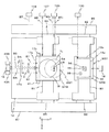
図1に戻り、前記ステージ装置50は、ベース盤12の上方に配置されたウエハステージWST及び計測ステージMST、これらのステージWST,MSTの位置情報を計測するY干渉計16,18等を含む干渉計システム118(図6参照)、及び露光の際などにウエハステージWSTの位置情報を計測するのに用いられる後述するエンコーダシステム、並びにステージWST,MSTを駆動するステージ駆動系124(図6参照)などを備えている。
Returning to FIG. 1, the
ウエハステージWST,計測ステージMSTそれぞれの底面には、不図示の非接触軸受、例えば真空予圧型空気静圧軸受(以下、「エアパッド」と呼ぶ)が複数ヶ所に設けられている。これらのエアパッドからベース盤12の上面に向けて噴出された加圧空気の静圧により、ベース盤12の上方にウエハステージWST,計測ステージMSTが数μm程度のクリアランスを介して非接触で支持されている。また、ステージWST,MSTは、ステージ駆動系124によって、所定平面(XY平面)内のY軸方向(図1における紙面内左右方向)及びX軸方向(図1における紙面直交方向)に独立して2次元駆動可能である。
On the bottom surfaces of wafer stage WST and measurement stage MST, non-contact bearings (not shown), for example, vacuum preload type static air bearings (hereinafter referred to as “air pads”) are provided at a plurality of locations. The wafer stage WST and measurement stage MST are supported in a non-contact manner above the
これをさらに詳述すると、床面上には、図2の平面図に示されるように、ベース盤12を挟んで、X軸方向の一側と他側に、Y軸方向に延びる一対のY軸固定子86,87が、それぞれ配置されている。Y軸固定子86、87は、例えばY軸方向に沿って所定間隔でかつ交互に配置されたN極磁石とS極磁石の複数の組から成る永久磁石群を内蔵する磁極ユニットによって構成されている。Y軸固定子86、87には、各2つのY軸可動子82,84及び83,85が、それぞれ非接触で係合した状態で設けられている。すなわち、合計4つのY軸可動子82、84、83、85は、XZ断面U字状のY軸固定子86又は87の内部空間に挿入された状態となっており、対応するY軸固定子86又は87に対して不図示のエアパッドをそれぞれ介して例えば数μm程度のクリアランスを介して非接触で支持されている。Y軸可動子82、84、83、85のそれぞれは、例えばY軸方向に沿って所定間隔で配置された電機子コイルを内蔵する電機子ユニットによって構成されている。すなわち、本実施形態では、電機子ユニットから成るY軸可動子82、84と磁極ユニットから成るY軸固定子86とによって、ムービングコイル型のY軸リニアモータがそれぞれ構成されている。同様にY軸可動子83、85とY軸固定子87とによって、ムービングコイル型のY軸リニアモータがそれぞれ構成されている。以下においては、上記4つのY軸リニアモータのそれぞれを、それぞれの可動子82、84、83、85と同一の符号を用いて、適宜、Y軸リニアモータ82、Y軸リニアモータ84、Y軸リニアモータ83、及びY軸リニアモータ85と呼ぶものとする。
More specifically, on the floor surface, as shown in the plan view of FIG. 2, a pair of Y extending in the Y-axis direction on one side and the other side in the X-axis direction with the
上記4つのY軸リニアモータのうち、2つのY軸リニアモータ82、83の可動子82,83は、X軸方向に延びるX軸固定子80の長手方向の一端と他端にそれぞれ固定されている。また、残り2つのY軸リニアモータ84、85の可動子84,85は、X軸方向に延びるX軸固定子81の一端と他端に固定されている。従って、X軸固定子80、81は、各一対のY軸リニアモータ82,83、84,85によって、Y軸に沿ってそれぞれ駆動される。
Among the four Y-axis linear motors, the
X軸固定子80,81のそれぞれは、例えばX軸方向に沿って所定間隔で配置された電機子コイルをそれぞれ内蔵する電機子ユニットによって構成されている。
Each of the
一方のX軸固定子81は、ウエハステージWSTの一部を構成するステージ本体91(図2では不図示、図1参照)に形成された不図示の開口に挿入状態で設けられている。このステージ本体91の上記開口の内部には、例えばX軸方向に沿って所定間隔でかつ交互に配置されたN極磁石とS極磁石の複数の組から成る永久磁石群を有する磁極ユニットが設けられている。この磁極ユニットとX軸固定子81とによって、ステージ本体91をX軸方向に駆動するムービングマグネット型のX軸リニアモータが構成されている。同様に、他方のX軸固定子80は、計測ステージMSTを構成するステージ本体92に形成された開口に挿入状態で設けられている。このステージ本体92の上記開口の内部には、ウエハステージWST側(ステージ本体91側)と同様の磁極ユニットが設けられている。この磁極ユニットとX軸固定子80とによって、計測ステージMSTをX軸方向に駆動するムービングマグネット型のX軸リニアモータが構成されている。
One
本実施形態では、ステージ駆動系124を構成する上記各リニアモータが、図6に示される主制御装置20によって制御される。なお、各リニアモータは、それぞれムービングマグネット型、ムービングコイル型のどちらか一方に限定されるものではなく、必要に応じて適宜選択することができる。
In this embodiment, each linear motor constituting the
なお、一対のY軸リニアモータ84,85がそれぞれ発生する推力を僅かに異ならせることで、ウエハステージWSTのヨーイング量(θz方向の回転量)の制御が可能である。また、一対のY軸リニアモータ82,83がそれぞれ発生する推力を僅かに異ならせることで、計測ステージMSTのヨーイング量の制御が可能である。
Note that the yawing amount (rotation amount in the θz direction) of wafer stage WST can be controlled by making the thrusts generated by the pair of Y-axis
ウエハステージWSTは、前述したステージ本体91と、該ステージ本体91上に搭載されたウエハテーブルWTBとを含む。このウエハテーブルWTB及びステージ本体91は、不図示のZレベリング機構(例えばボイスコイルモータ等を含む)によって、ベース盤12及びX軸固定子81に対してZ軸方向、θx方向、及びθy方向に相対的に微小駆動される。すなわち、ウエハテーブルWTBはXY平面(又は投影光学系PLの像面)に対してZ軸方向に微動可能かつ傾斜(チルト)可能となっている。なお、図6では、上記各リニアモータ及びZレベリング機構、並びに計測ステージMSTの駆動系を含んで、ステージ駆動系124として示されている。また、ウエハテーブルWTBはX軸、Y軸、及びθz方向の少なくとも1つについても微動可能に構成しても良い。
Wafer stage WST includes
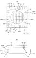
前記ウエハテーブルWTB上には、ウエハWを真空吸着等によって保持するウエハホルダ(不図示)が設けられている。ウエハホルダはウエハテーブルWTBと一体に形成しても良いが、本実施形態ではウエハホルダとウエハテーブルWTBとを別々に構成し、例えば真空吸着などによってウエハホルダをウエハテーブルWTBの凹部内に固定している。また、ウエハテーブルWTBの上面には、ウエハホルダ上に載置されるウエハの表面とほぼ面一となる、液体Lqに対して撥液化処理された表面(撥液面)を有し、かつ外形(輪郭)が矩形でその中央部にウエハホルダ(ウエハの載置領域)よりも一回り大きな円形の開口が形成されたプレート(撥液板)28が設けられている。プレート28は、低熱膨張率の材料、例えばガラス又はセラミックス(ショット社のゼロデュア(商品名)、Al2O3あるいはTiCなど)から成り、その表面には、例えばフッ素樹脂材料、ポリ四フッ化エチレン(テフロン(登録商標))等のフッ素系樹脂材料、アクリル系樹脂材料あるいはシリコン系樹脂材料などにより撥液膜が形成される。さらにプレート28は、図4(A)のウエハテーブルWTB(ウエハステージWST)の平面図に示されるように、円形の開口を囲む、外形(輪郭)が矩形の第1撥液領域28aと、第1撥液領域28aの周囲に配置される矩形枠状(環状)の第2撥液領域28bとを有する。第1撥液領域28aは、例えば露光動作時、ウエハの表面からはみ出す液浸領域14の少なくとも一部が形成され、第2撥液領域28bは、後述のエンコーダシステムのためのスケール(格子部)が形成される。なお、プレート28はその表面の少なくとも一部がウエハの表面と面一でなくても良い、すなわち異なる高さであっても良い。また、プレート28は単一のプレートでも良いが、本実施形態では複数のプレート、例えば第1及び第2撥液領域28a、28bにそれぞれ対応する第1及び第2撥液板を組み合わせて構成する。本実施形態では、前述の如く液体Lqとして純水を用いるので、以下では第1及び第2撥液領域28a、28bをそれぞれ第1及び第2撥水板28a、28bとも呼ぶ。
A wafer holder (not shown) for holding the wafer W by vacuum suction or the like is provided on the wafer table WTB. Although the wafer holder may be formed integrally with wafer table WTB, in this embodiment, the wafer holder and wafer table WTB are separately configured, and the wafer holder is fixed in the recess of wafer table WTB by, for example, vacuum suction. In addition, the upper surface of wafer table WTB has a surface (liquid repellent surface) that has been subjected to a liquid repellent treatment with respect to liquid Lq and is substantially flush with the surface of the wafer placed on the wafer holder, and has an outer shape ( A plate (liquid repellent plate) 28 having a rectangular outline and a circular opening that is slightly larger than the wafer holder (wafer mounting region) is provided at the center thereof. The
この場合、内側の第1撥水板28aには、露光光ILが照射されるのに対し、外側の第2撥水板28bには、露光光ILが殆ど照射されない。このことを考慮して、本実施形態では、第1撥水板28aの表面には、露光光IL(この場合、真空紫外域の光)に対する耐性が十分にある撥水コートが施された第1撥水領域が形成され、第2撥水板28bには、その表面に第1撥水領域に比べて露光光ILに対する耐性が劣る撥水コートが施された第2撥水領域が形成されている。一般にガラス板には、露光光IL(この場合、真空紫外域の光)に対する耐性が十分にある撥水コートを施し難いので、このように第1撥水板28aとその周囲の第2撥水板28bとの2つの部分に分離することは効果的である。なお、これに限らず、同一のプレートの上面に露光光ILに対する耐性が異なる2種類の撥水コートを施して、第1撥水領域、第2撥水領域を形成しても良い。また、第1及び第2撥水領域で撥水コートの種類が同一でも良い。例えば、同一のプレートに1つの撥水領域を形成するだけでも良い。
In this case, the inner first
また、図4(A)から明らかなように、第1撥水板28aの+Y側の端部には、そのX軸方向の中央部に長方形の切り欠きが形成され、この切り欠きと第2撥水板28bとで囲まれる長方形の空間の内部(切り欠きの内部)に計測プレート30が埋め込まれている。計測プレート30の長手方向の中央(ウエハテーブルWTBのセンターラインLL上)には、基準マークFMが形成されるとともに、該基準マークFMのX軸方向の一側と他側に、基準マークFMの中心に関して対称な配置で一対の空間像計測スリットパターンSLが形成されている。各空間像計測スリットパターンSLとしては、一例として、Y軸方向とX軸方向とに沿った辺を有するL字状のスリットパターンを用いることができる。
As is clear from FIG. 4A, a rectangular notch is formed at the center of the first
そして、上記各空間像計測スリットパターンSL下方のウエハステージWST部分には、図4(B)に示されるように、その内部に対物レンズ、ミラー、リレーレンズなどを含む光学系が収納されたL字状の筐体36が、ウエハテーブルWTBからステージ本体91の内部の一部を貫通する状態で、一部埋め込み状態で取り付けられている。筐体36は、図示は省略されているが、上記一対の空間像計測スリットパターンSLに対応して一対設けられている。
Then, as shown in FIG. 4B, the portion of wafer stage WST below each aerial image measurement slit pattern SL accommodates therein an optical system including an objective lens, a mirror, a relay lens, and the like. A character-shaped
上記筐体36内部の光学系は、空間像計測スリットパターンSLを上方から下方に透過した照明光ILを、L字状の経路に沿って導き、−Y方向に向けて射出する。なお、以下においては、便宜上、筐体36内部の光学系を筐体36と同一の符号を用いて送光系36と記述する。
The optical system inside the
さらに、第2撥水板28bの上面には、その4辺のそれぞれに沿って所定ピッチで多数の格子線が直接形成されている。これをさらに詳述すると、第2撥水板28bのX軸方向一側と他側(図4(A)における左右両側)の領域には、Yスケール39Y1,39Y2がそれぞれ形成されている。Yスケール39Y1,39Y2はそれぞれ、例えばX軸方向を長手方向とする格子線38が所定ピッチでY軸に平行な方向(Y軸方向)に沿って形成される、Y軸方向を周期方向とする反射型の格子(例えば回折格子)によって構成されている。
Furthermore, a large number of grid lines are directly formed on the upper surface of the second
同様に、第2撥水板28bのY軸方向一側と他側(図4(A)における上下両側)の領域には、Xスケール39X1,39X2がそれぞれ形成されている。Xスケール39X1,39X2はそれぞれ、例えばY軸方向を長手方向とする格子線37が所定ピッチでX軸に平行な方向(X軸方向)に沿って形成される、X軸方向を周期方向とする反射型の格子(例えば回折格子)によって構成されている。上記各スケールとしては、第2撥水板28bの表面に例えばホログラム等により反射型の回折格子RG(図8(A))が作成されたものが用いられている。この場合、各スケールには狭いスリットや溝等から成る格子が目盛りとして所定間隔(ピッチ)で刻まれている。各スケールに用いられる回折格子の種類は限定されるものではなく、機械的に溝等が形成されたもののみならず、例えば、感光性樹脂に干渉縞を焼き付けて作成したものであっても良い。但し、各スケールは、例えば薄板状のガラスに上記回折格子の目盛りを、例えば138nm〜4μmの間のピッチ、例えば1μmピッチで刻んで作成されている。これらスケールは前述の撥液膜(撥水膜)で覆われている。なお、図4(A)では、図示の便宜上から、格子のピッチは、実際のピッチに比べて格段に広く図示されている。その他の図においても同様である。
Similarly, X scales 39X 1 and 39X 2 are formed in regions on one side and the other side (upper and lower sides in FIG. 4A) of the second
このように、本実施形態では、第2撥水板28bそのものがスケールを構成するので、第2撥水板28bとして低熱膨張率のガラス板を用いることとしたものである。しかし、これに限らず、格子が形成された低熱膨張率のガラス板などから成るスケール部材を、局所的な伸縮が生じないように、例えば板ばね(又は真空吸着)等によりウエハテーブルWTBの上面に固定しても良く、この場合には、全面に同一の撥水コートが施された撥水板をプレート28に代えて用いても良い。あるいは、ウエハテーブルWTBを低熱膨張率の材料で形成することも可能であり、かかる場合には、一対のYスケールとXスケールとは、そのウエハテーブルWTBの上面に直接形成しても良い。
Thus, in this embodiment, since the second
ウエハテーブルWTBの−Y端面,−X端面には、それぞれ鏡面加工が施され、図2に示される反射面17a,反射面17bが形成されている。干渉計システム118(図6参照)の一部を構成するY干渉計16及びX干渉計126、127、128(図1では、X干渉計126〜128は不図示、図2参照)は、これらの反射面17a,17bにそれぞれ干渉計ビーム(測長ビーム)を投射して、それぞれの反射光を受光することにより、各反射面の基準位置(一般には投影ユニットPU側面に固定ミラーを配置し、そこを基準面とする)からの変位、すなわちウエハステージWSTのXY平面内の位置情報を計測し、この計測した位置情報を主制御装置20に供給する。本実施形態では、後述するように、上記各干渉計としては、一部を除いて、測長軸を複数有する多軸干渉計が用いられている。
The -Y end surface and -X end surface of wafer table WTB are mirror-finished to form reflecting
一方、ステージ本体91の−Y側の側面には、図1及び図4(B)に示されるように、X軸方向を長手方向とする移動鏡41が、不図示のキネマティック支持機構を介して取り付けられている。
On the other hand, on the side surface on the −Y side of the stage
移動鏡41に対向して、該移動鏡41に測長ビームを照射する、干渉計システム118(図6参照)の一部を構成する一対のZ干渉計43A,43Bが設けられている(図1及び図2参照)。これをさらに詳述すると、移動鏡41は、図2及び図4(B)を総合するとわかるように、X軸方向の長さがウエハテーブルWTBの反射面17aよりも、少なくともZ干渉計43A,43Bの間隔分、長く設計されている。また、移動鏡41は、長方形と等脚台形とを一体化したような六角形の断面形状を有する部材から成る。移動鏡41の−Y側の面に鏡面加工が施され、3つの反射面41b、41a、41cが形成されている。
A pair of
反射面41aは、移動鏡41の−Y側の端面を構成し、XZ平面と平行に且つX軸方向に延びている。反射面41bは、反射面41aの+Z側に隣接する面を構成し、XZ平面に対して所定角度だけ図4(B)における時計回り方向に傾斜した面と平行に且つX軸方向に延びている。反射面41cは、反射面41aの−Z側に隣接する面を構成し、反射面41aを挟んで反射面41bと対称に設けられている。
The reflecting
Z干渉計43A、43Bは、図1及び図2を総合するとわかるように、Y干渉計16のX軸方向の一側と他側にほぼ同一距離離れて、且つY干渉計16より幾分低い位置にそれぞれ配置されている。
The
Z干渉計43A、43Bそれぞれから、図1に示されるように、Y軸方向に沿う測長ビームB1が反射面41bに向けて投射されるとともに、Y軸方向に沿う測長ビームB2が反射面41c(図4(B)参照)に向けて投射されるようになっている。本実施形態では、反射面41bで反射された測長ビームB1と直交する反射面を有する固定鏡47A、及び反射面41cで反射された測長ビームB2と直交する反射面を有する固定鏡47Bが、移動鏡41から−Y方向に所定距離離れた位置に測長ビームB1,B2に干渉しない状態で、それぞれX軸方向に延設されている。
As shown in FIG. 1, each of the
固定鏡47A、47Bは、例えば投影ユニットPUを支持するフレーム(不図示)に設けられた同一の支持体(不図示)に支持されている。なお、固定鏡47A、47Bは前述の計測フレームなどに設けても良い。また、本実施形態では、3つの反射面41b、41a、41cを有する移動鏡41と、固定鏡47A、47Bとを設けるものとしたが、これに限らず、例えば45度の斜面を有する移動鏡をステージ本体91の側面に設け、ウエハステージWSTの上方に固定鏡を配置する構成としても良い。この場合、固定鏡を前述の支持体あるいは計測フレームなどに設ければ良い。
The fixed mirrors 47A and 47B are supported by, for example, the same support (not shown) provided on a frame (not shown) that supports the projection unit PU. The fixed mirrors 47A and 47B may be provided on the above-described measurement frame or the like. In this embodiment, the
Y干渉計16は、図2に示されるように、投影光学系PLの投影中心(光軸AX、図1参照)を通るY軸に平行な直線から同一距離−X側,+X側に離れたY軸方向の測長軸に沿って測長ビームB41,B42をウエハテーブルWTBの反射面17aに投射し、それぞれの反射光を受光することで、ウエハテーブルWTBの測長ビームB41,B42の照射点におけるY軸方向の位置(Y位置)を検出している。なお、図1では、測長ビームB41,B42が代表的に測長ビームB4として示されている。
As shown in FIG. 2, the
また、Y干渉計16は、測長ビームB41,B42との間にZ軸方向に所定間隔をあけてY軸方向の測長軸に沿って測長ビームB3を反射面41aに向けて投射し、反射面41aで反射した測長ビームB3を受光することにより、移動鏡41の反射面41a(すなわちウエハステージWST)のY位置を検出している。
Further, the
主制御装置20は、Y干渉計16の測長ビームB41,B42に対応する測長軸の計測値の平均値に基づいて反射面17a、すなわちウエハテーブルWTB(ウエハステージWST)のY位置(より正しくは、Y軸方向の変位ΔY)を算出する。また、主制御装置20は、測長ビームB41,B42に対応する測長軸の計測値の差より、ウエハテーブルWTBのZ軸回りの回転方向(θz方向)の変位(ヨーイング量)Δθz(Y)を算出する。また、主制御装置20は、反射面17a及び反射面41aにおけるY位置(Y軸方向の変位ΔY)に基づいて、ウエハステージWSTのθx方向の変位(ピッチング量)Δθxを算出する。
また、X干渉計126は、図2に示されるように、投影光学系PLの光軸を通るX軸方向の直線LHに関して同一距離離れた2軸の測長軸に沿って測長ビームB51,B52をウエハテーブルWTBに投射しており、主制御装置20は、測長ビームB51,B52に対応する測長軸の計測値に基づいて、ウエハテーブルWTBのX軸方向の位置(X位置、より正しくは、X軸方向の変位ΔX)を算出する。また、主制御装置20は、測長ビームB51,B52に対応する測長軸の計測値の差より、ウエハテーブルWTBのθz方向の変位(ヨーイング量)Δθz(X)を算出する。なお、X干渉計126から得られるΔθz(X)とY干渉計16から得られるΔθz(Y)は互いに等しく、ウエハテーブルWTBのθz方向への変位(ヨーイング量)Δθzを代表する。
Further,
また、図2に点線で示されるように、X干渉計128からX軸に平行な測長軸に沿って測長ビームB7が射出される。このX干渉計128は、実際には、後述するアンローディングポジションUPとローディングポジションLP(図3参照)とを結ぶX軸に平行な測長軸に沿って、アンローディングポジションUPとローディングポジションLPの近傍に位置するウエハテーブルWTBの反射面17bに測長ビームB7を投射する。また、図2に示されるように、X干渉計127から測長ビームB6が、ウエハテーブルWTBの反射面17bに投射される。実際には、測長ビームB6は、プライマリアライメント系AL1の検出中心を通るX軸に平行な測長軸に沿って、ウエハテーブルWTBの反射面17bに投射される。
Further, as indicated by a dotted line in FIG. 2, a measurement beam B7 is emitted from the
主制御装置20は、X干渉計127の測長ビームB6の計測値、及びX干渉計128の測長ビームB7の計測値からも、ウエハテーブルWTBのX軸方向の変位ΔXを求めることができる。ただし、3つのX干渉計126,127,128の配置がY軸方向に関して異なっており、X干渉計126は図14に示される露光時に、X干渉計127は図21等に示されるウエハアライメント時に、X干渉計128は図18及び図19に示されるウエハのロード時及び図17に示されるアンロード時に使用される。
また、Z干渉計43A、43Bそれぞれからは、Y軸に沿う測長ビームB1、B2が、移動鏡41に向けて投射される。これらの測長ビームB1、B2は、移動鏡41の反射面41b,41cのそれぞれに所定の入射角(θ/2とする)で入射する。そして、測長ビームB1、B2は、反射面41b、41cでそれぞれ反射されて、固定鏡47A、47Bの反射面に垂直に入射する。そして、固定鏡47A、47Bの反射面で反射された測長ビームB1、B2は、再度反射面41b,41cでそれぞれ反射されて(入射時の光路を逆向きに戻り)Z干渉計43A、43Bで受光される。
Further, from each of the
ここで、ウエハステージWST(すなわち移動鏡41)のY軸方向への変位をΔYo、Z軸方向への変位をΔZoとすると、Z干渉計43A、43Bで受光される測長ビームB1の光路長変化ΔL1及び測長ビームB2の光路長変化ΔL2は、それぞれ以下の式(1)、(2)で表される。
Here, if the displacement of wafer stage WST (that is, moving mirror 41) in the Y-axis direction is ΔYo and the displacement in Z-axis direction is ΔZo, the optical path length of measurement beam B1 received by
ΔL1=ΔYo×(1+cosθ)−ΔZo×sinθ …(1)
ΔL2=ΔYo×(1+cosθ)+ΔZo×sinθ …(2)
従って、式(1)、(2)からΔZo及びΔYoは次式(3)、(4)で求められる。
ΔL1 = ΔYo × (1 + cos θ) −ΔZo × sin θ (1)
ΔL2 = ΔYo × (1 + cos θ) + ΔZo × sin θ (2)
Therefore, ΔZo and ΔYo are obtained by the following equations (3) and (4) from the equations (1) and (2).
ΔZo=(ΔL2−ΔL1)/2sinθ …(3)
ΔYo=(ΔL1+ΔL2)/{2(1+cosθ)} …(4)
ΔZo = (ΔL2−ΔL1) / 2sin θ (3)
ΔYo = (ΔL1 + ΔL2) / {2 (1 + cos θ)} (4)
上記の変位ΔZo、ΔYoは、Z干渉計43A、43Bのそれぞれで求められる。そこで、Z干渉計43Aで求められる変位をΔZoR、ΔYoRとし、Z干渉計43Bで求められる変位をΔZoL、ΔYoLとする。そして、Z干渉計43A、43Bそれぞれが投射する測長ビームB1、B2がX軸方向に離間する距離をDとする(図2参照)。かかる前提の下で、移動鏡41(すなわちウエハステージWST)のθz方向への変位(ヨーイング量)Δθz、及び移動鏡41(すなわちウエハステージWST)のθy方向への変位(ローリング量)Δθyは次式(5)、(6)で求められる。
The displacements ΔZo and ΔYo are determined by the
Δθz≒(ΔYoR−ΔYoL)/D …(5)
Δθy≒(ΔZoL−ΔZoR)/D …(6)
従って、主制御装置20は、上記式(3)〜式(6)を用いることで、Z干渉計43A、43Bの計測結果に基づいて、ウエハステージWSTの4自由度の変位ΔZo、ΔYo、Δθz、Δθyを算出することができる。
Δθz≈ (ΔYoR−ΔYoL) / D (5)
Δθy≈ (ΔZoL−ΔZoR) / D (6)
Therefore,
このように、主制御装置20は、干渉計システム118の計測結果から、6自由度方向(Z、X、Y、θz、θx、θy方向)に関するウエハステージWSTの変位を求めることができる。なお、本実施形態では干渉計システム118がウエハステージWSTの6自由度方向の位置情報を計測可能であるものとしたが、計測方向は6自由度方向に限られず5自由度以下の方向でも良い。
Thus,
なお、本実施形態では、ウエハステージWST(91,WTB)が6自由度で移動可能な単一のステージである場合について説明したが、これに限らず、XY平面内で自在に移動可能なステージ本体91と、該ステージ本体91上に搭載され、ステージ本体91に対して少なくともZ軸方向、θx方向及びθy方向に相対的に微小駆動可能なウエハテーブルWTBとを含んでウエハステージWSTを構成しても良い。この場合、前述の移動鏡41はウエハテーブルWTBに設けられる。また、反射面17a,反射面17bの代わりに、ウエハテーブルWTBに平面ミラーから成る移動鏡を設けても良い。
In this embodiment, the case where wafer stage WST (91, WTB) is a single stage movable with six degrees of freedom has been described. However, the present invention is not limited to this, and the stage can be freely moved in the XY plane. A wafer stage WST is configured to include a
但し、本実施形態では、ウエハステージWST(ウエハテーブルWTB)のXY平面内の位置情報(θz方向の回転情報を含む3自由度方向の位置情報)は、主として、後述するエンコーダシステムによって計測され、干渉計16,126,127の計測値は、そのエンコーダシステムの計測値の長期的変動(例えばスケールの経時的な変形などによる)を補正(較正)する場合、エンコーダの出力異常発生時のバックアップの場合などに補助的に用いられる。なお、本実施形態では、ウエハステージWSTの6自由度方向の位置情報のうち、X軸方向、Y軸方向及びθz方向を含む3自由度方向の位置情報は後述のエンコーダシステムによって計測し、残りの3自由度方向、すなわちZ軸方向、θx方向及びθy方向の位置情報は、後述の複数のZセンサを有する計測システムによって計測される。ここで、残りの3自由度方向の位置情報は、計測システムと干渉計システム118の両方によって計測しても良い。例えば、計測システムによってZ軸方向及びθy方向の位置情報を計測し、干渉計システム118によってθx方向の位置情報を計測しても良い。
However, in the present embodiment, position information in the XY plane of wafer stage WST (wafer table WTB) (position information in three degrees of freedom including rotation information in the θz direction) is mainly measured by an encoder system described later. The measured values of the
なお、干渉計システム118はその少なくとも一部(例えば、光学系など)が、投影ユニットPUを保持するメインフレームに設けられる、あるいは前述の如く吊り下げ支持される投影ユニットPUと一体に設けられても良いが、本実施形態では前述した計測フレームに設けられるものとする。
The
前記計測ステージMSTは、前述したステージ本体92と、該ステージ本体92上に搭載された計測テーブルMTBとを含んでいる。計測テーブルMTBは、不図示のZレベリング機構を介してステージ本体92上に搭載されている。しかしながら、これに限らず、例えば、計測テーブルMTBを、ステージ本体92に対してX軸方向、Y軸方向及びθz方向に微動可能に構成したいわゆる粗微動構造の計測ステージMSTを採用しても良いし、あるいは、計測テーブルMTBをステージ本体92に固定し、その計測テーブルMTBとステージ本体92とを含む計測ステージMSTの全体を6自由度方向に駆動可能な構成にしても良い。
The measurement stage MST includes the stage
計測テーブルMTB(及びステージ本体92)には、各種計測用部材が設けられている。この計測用部材としては、例えば、図2及び図5(A)に示されるように、投影光学系PLの像面上で照明光ILを受光するピンホール状の受光部を有する照度むらセンサ94、投影光学系PLにより投影されるパターンの空間像(投影像)を計測する空間像計測器96、及び例えば国際公開第03/065428号などに開示されているシャック−ハルトマン(Shack-Hartman)方式の波面収差計測器98などが採用されている。波面収差計測器98としては、例えば国際公開第99/60361号(対応欧州特許出願公開第1079223号明細書)に開示されるものも用いることができる。
Various measurement members are provided on the measurement table MTB (and the stage main body 92). As this measuring member, for example, as shown in FIGS. 2 and 5A, an
照度むらセンサ94としては、例えば特開昭57−117238号公報(対応する米国特許第4,465,368号明細書)などに開示されるものと同様の構成のものを用いることができる。また、空間像計測器96としては、例えば特開2002−14005号公報(対応する米国特許出願公開第2002/0041377号明細書)などに開示されるものと同様の構成のものを用いることができる。なお、本実施形態では3つの計測用部材(94、96、98)を計測ステージMSTに設けるものとしたが、計測用部材の種類、及び/又は数などはこれに限られない。計測用部材として、例えば投影光学系PLの透過率を計測する透過率計測器、及び/又は、前述の局所液浸装置8、例えばノズルユニット32(あるいは先端レンズ191)などを観察する計測器などを用いても良い。さらに、計測用部材と異なる部材、例えばノズルユニット32、先端レンズ191などを清掃する清掃部材などを計測ステージMSTに搭載しても良い。
As the
本実施形態では、図5(A)からもわかるように、使用頻度の高いセンサ類、照度むらセンサ94及び空間像計測器96などは、計測ステージMSTのセンターラインCL(中心を通るY軸)上に配置されている。このため、本実施形態では、これらのセンサ類を用いた計測を、計測ステージMSTをX軸方向に移動させることなく、Y軸方向にのみ移動させて行うことができる。
In this embodiment, as can be seen from FIG. 5A, the frequently used sensors, the
上記各センサに加え、例えば特開平11−16816号公報(対応する米国特許出願公開第2002/0061469号明細書)などに開示される、投影光学系PLの像面上で照明光ILを受光する所定面積の受光部を有する照度モニタを採用しても良く、この照度モニタもセンターライン上に配置することが望ましい。 In addition to the sensors described above, illumination light IL is received on the image plane of the projection optical system PL disclosed in, for example, Japanese Patent Application Laid-Open No. 11-16816 (corresponding US Patent Application Publication No. 2002/0061469). An illuminance monitor having a light receiving portion with a predetermined area may be adopted, and it is desirable that this illuminance monitor is also arranged on the center line.
なお、本実施形態では、投影光学系PLと液体(水)Lqとを介して露光光(照明光)ILによりウエハWを露光する液浸露光が行われるのに対応して、照明光ILを用いる計測に使用される上記の照度むらセンサ94(及び照度モニタ)、空間像計測器96、並びに波面収差計測器98では、投影光学系PL及び水Lqを介して照明光ILを受光することとなる。また、各センサは、例えば光学系などの一部だけが計測テーブルMTB(及びステージ本体92)に搭載されていても良いし、センサ全体を計測テーブルMTB(及びステージ本体92)に配置するようにしても良い。
In the present embodiment, the illumination light IL is applied in response to the immersion exposure that exposes the wafer W with the exposure light (illumination light) IL via the projection optical system PL and the liquid (water) Lq. The illuminance unevenness sensor 94 (and the illuminance monitor), the aerial
計測ステージMSTのステージ本体92には、図5(B)に示されるように、その−Y側の端面に、枠状の取付部材42が固定されている。また、ステージ本体92の−Y側の端面には、取付部材42の開口内部のX軸方向の中心位置近傍に、前述した一対の送光系36に対向し得る配置で、一対の受光系44が固定されている。各受光系44は、リレーレンズなどの光学系と、受光素子、例えばフォトマルチプライヤチューブなどと、これらを収納する筐体とによって構成されている。図4(B)及び図5(B)、並びにこれまでの説明からわかるように、本実施形態では、ウエハステージWSTと計測ステージMSTとが、Y軸方向に関して所定距離以内に近接した状態(接触状態を含む)では、計測プレート30の各空間像計測スリットパターンSLを透過した照明光ILが前述の各送光系36で案内され、各受光系44内部の各受光素子で受光される。すなわち、計測プレート30、送光系36及び受光系44によって、前述した特開2002−14005号公報(対応する米国特許出願公開第2002/0041377号明細書)などに開示されるものと同様の、空間像計測装置45が構成される(図6参照)。
As shown in FIG. 5B, a frame-shaped
前記取付部材42の上には、断面矩形の棒状部材から成る基準部材としてのコンフィデンシャルバー(以下、「CDバー」と略述する)46がX軸方向に延設されている。このCDバー46は、フルキネマティックマウント構造によって、計測ステージMST上にキネマティックに支持されている。
On the mounting
CDバー46は、原器(計測基準)となるため、低熱膨張率の光学ガラスセラミックス、例えば、ショット社のゼロデュア(商品名)などがその素材として採用されている。このCDバー46の上面(表面)は、いわゆる基準平面板と同程度にその平坦度が高く設定されている。また、このCDバー46の長手方向の一側と他側の端部近傍には、図5(A)に示されるように、Y軸方向を周期方向とする基準格子(例えば回折格子)52がそれぞれ形成されている。この一対の基準格子52は、相互に所定距離(Lとする)を隔ててCDバー46のX軸方向の中心、すなわち前述のセンターラインCLに関して対称な配置で形成されている。
Since the
また、このCDバー46の上面には、図5(A)に示されるような配置で複数の基準マークMが形成されている。この複数の基準マークMは、同一ピッチでY軸方向に関して3行の配列で形成され、各行の配列がX軸方向に関して互いに所定距離だけずれて形成されている。各基準マークMとしては、後述するプライマリアライメント系、セカンダリアライメント系によって検出可能な寸法の2次元マークが用いられている。基準マークMはその形状(構成)が前述の基準マークFMと異なっても良いが、本実施形態では基準マークMと基準マークFMとは同一の構成であり、かつウエハWのアライメントマークとも同一の構成となっている。なお、本実施形態ではCDバー46の表面、及び計測テーブルMTB(前述の計測用部材を含んでも良い)の表面もそれぞれ撥液膜(撥水膜)で覆われている。
A plurality of reference marks M are formed on the upper surface of the
計測テーブルMTBの+Y端面、−X端面も前述したウエハテーブルWTBと同様の反射面19a、19bが形成されている(図2及び図5(A)参照)。干渉計システム118(図6参照)のY干渉計18、X干渉計130(図1では、X干渉計130は不図示、図2参照)は、これらの反射面19a、19bに、図2に示されるように、干渉計ビーム(測長ビーム)を投射して、それぞれの反射光を受光することにより、各反射面の基準位置からの変位、すなわち計測ステージMSTの位置情報(例えば、少なくともX軸及びY軸方向の位置情報とθz方向の回転情報とを含む)を計測し、この計測値が主制御装置20に供給される。
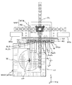
本実施形態の露光装置100では、図1では図面の錯綜を避ける観点から図示が省略されているが、実際には、図3に示されるように、投影ユニットPUの中心(投影光学系PLの光軸AX、本実施形態では前述の露光領域IAの中心とも一致)を通りかつY軸と平行な直線LV上で、その光軸から−Y側に所定距離隔てた位置に検出中心を有するプライマリアライメント系AL1が配置されている。このプライマリアライメント系AL1は、支持部材54を介して不図示のメインフレームの下面に固定されている。このプライマリアライメント系AL1を挟んで、X軸方向の一側と他側には、その直線LVに関してほぼ対称に検出中心が配置されるセカンダリアライメント系AL21,AL22と、AL23,AL24とが、それぞれ設けられている。すなわち、5つのアライメント系AL1,AL21〜AL24はその検出中心がX軸方向に関して異なる位置に配置されている、すなわちX軸方向に沿って配置されている。
In the
各セカンダリアライメント系AL2n(n=1〜4)は、セカンダリアライメント系AL24について代表的に示されるように、回転中心Oを中心として図3における時計回り及び反時計回りに所定角度範囲で回動可能なアーム56n(n=1〜4)の先端(回動端)に固定されている。本実施形態では、各セカンダリアライメント系AL2nはその一部(例えば、アライメント光を検出領域に照射し、かつ検出領域内の対象マークから発生する光を受光素子に導く光学系を少なくとも含む)がアーム56nに固定され、残りの一部は投影ユニットPUを保持するメインフレームに設けられる。セカンダリアライメント系AL21,AL22,AL23,AL24はそれぞれ、回転中心Oを中心として回動することで、X位置が調整される。すなわち、セカンダリアライメント系AL21,AL22,AL23,AL24はその検出領域(又は検出中心)が独立にX軸方向に可動である。従って、プライマリアライメント系AL1及びセカンダリアライメント系AL21,AL22,AL23,AL24はX軸方向に関してその検出領域の相対位置が調整可能となっている。なお、本実施形態では、アームの回動によりセカンダリアライメント系AL21,AL22,AL23,AL24のX位置が調整されるものとしたが、これに限らず、セカンダリアライメント系AL21,AL22,AL23,AL24をX軸方向に往復駆動する駆動機構を設けても良い。また、セカンダリアライメント系AL21,AL22,AL23,AL24の少なくとも1つをX軸方向だけでなくY軸方向にも可動として良い。なお、各セカンダリアライメント系AL2nはその一部がアーム56nによって移動されるので、不図示のセンサ、例えば干渉計、あるいはエンコーダなどによって、アーム56nに固定されるその一部の位置情報が計測可能となっている。このセンサは、セカンダリアライメント系AL2nのX軸方向の位置情報を計測するだけでも良いが、他の方向、例えばY軸方向、及び/又は回転方向(θx及びθy方向の少なくとも一方を含む)の位置情報も計測可能として良い。 Each secondary alignment system AL2 n (n = 1 to 4) rotates in a predetermined angle range clockwise and counterclockwise in FIG. 3 around the rotation center O as representatively shown for the secondary alignment system AL2 4 . The movable arm 56 n (n = 1 to 4) is fixed to the tip (rotating end). In the present embodiment, each secondary alignment system AL2 n includes a part thereof (for example, at least an optical system that irradiates the detection region with the alignment light and guides the light generated from the target mark in the detection region to the light receiving element). It is fixed to the arm 56 n and the remaining part is provided on the main frame that holds the projection unit PU. The secondary alignment systems AL2 1 , AL2 2 , AL2 3 , AL2 4 are each rotated about the rotation center O to adjust the X position. That is, the secondary alignment systems AL2 1 , AL2 2 , AL2 3 , AL2 4 have their detection areas (or detection centers) independently movable in the X-axis direction. Therefore, the primary alignment system AL1 and the secondary alignment systems AL2 1 , AL2 2 , AL2 3 , AL2 4 can adjust the relative positions of their detection areas in the X-axis direction. In the present embodiment, the X position of the secondary alignment systems AL2 1 , AL2 2 , AL2 3 , AL2 4 is adjusted by the rotation of the arm, but this is not limiting, and the secondary alignment systems AL2 1 , AL2 are not limited thereto. 2 , AL2 3 , AL2 4 may be provided with a driving mechanism that reciprocates in the X-axis direction. Further, at least one of the secondary alignment systems AL2 1 , AL2 2 , AL2 3 , AL2 4 may be movable not only in the X axis direction but also in the Y axis direction. Since each secondary alignment system AL2 n part is moved by arm 56 n, a sensor (not shown), such as by an interferometer or an encoder, and a part of the location information that is fixed to arm 56 n Measurement is possible. This sensor may only measure the positional information of the secondary alignment system AL2 n in the X-axis direction, but in other directions, for example, the Y-axis direction and / or the rotational direction (including at least one of the θx and θy directions). The position information may be measurable.
各アーム56nの上面には、差動排気型のエアベアリングから成るバキュームパッド58n(n=1〜4)が設けられている。また、アーム56nは、モータ等を含む回転駆動機構60n(n=1〜4、図3では不図示、図6参照)によって、主制御装置20の指示に応じて回動可能である。主制御装置20は、アーム56nの回転調整後に、各バキュームパッド58nを作動させて各アーム56nを不図示のメインフレームに吸着固定する。これにより、各アーム56nの回転角度調整後の状態、すなわち、プライマリアライメント系AL1及び4つのセカンダリアライメント系AL21〜AL24の所望の位置関係が維持される。
A vacuum pad 58 n (n = 1 to 4) made of a differential exhaust type air bearing is provided on the upper surface of each arm 56 n . Further, the arm 56 n can be rotated in accordance with an instruction from the
なお、メインフレームのアーム56nに対向する部分が磁性体であるならば、バキュームパッド58に代えて電磁石を採用しても良い。 If the portion of the main frame facing the arm 56 n is a magnetic material, an electromagnet may be used instead of the vacuum pad 58.
本実施形態では、プライマリアライメント系AL1及び4つのセカンダリアライメント系AL21〜AL24のそれぞれとして、例えばウエハ上のレジストを感光させないブロードバンドな検出光束を対象マークに照射し、その対象マークからの反射光により受光面に結像された対象マークの像と不図示の指標(各アライメント系内に設けられた指標板上の指標パターン)の像とを撮像素子(CCD等)を用いて撮像し、それらの撮像信号を出力する画像処理方式のFIA(Field Image Alignment)系が用いられている。プライマリアライメント系AL1及び4つのセカンダリアライメント系AL21〜AL24のそれぞれからの撮像信号は、図6の主制御装置20に供給される。
In the present embodiment, as each of the primary alignment system AL1 and the four secondary alignment systems AL2 1 to AL2 4 , for example, a broadband detection light beam that does not expose the resist on the wafer is irradiated to the target mark, and the reflected light from the target mark The target mark image formed on the light receiving surface and the image of the index (not shown) (the index pattern on the index plate provided in each alignment system) are imaged using an image sensor (CCD, etc.) An image processing type FIA (Field Image Alignment) system that outputs the image pickup signal is used. Imaging signals from each of the primary alignment system AL1 and the four secondary alignment systems AL2 1 to AL2 4 are supplied to the
なお、上記各アライメント系としては、FIA系に限らず、コヒーレントな検出光を対象マークに照射し、その対象マークから発生する散乱光又は回折光を検出する、あるいはその対象マークから発生する2つの回折光(例えば同次数の回折光、あるいは同方向に回折する回折光)を干渉させて検出するアライメントセンサを単独であるいは適宜組み合わせて用いることは勿論可能である。また、本実施形態では5つのアライメント系AL1、AL21〜AL24を設けるものとしているが、その数は5つに限られるものでなく、2つ以上かつ4つ以下、あるいは6つ以上でも良いし、奇数ではなく偶数でも良い。さらに、本実施形態では、5つのアライメント系AL1、AL21〜AL24は、支持部材54を介して投影ユニットPUを保持するメインフレームの下面に固定されるものとしたが、これに限らず、例えば前述した計測フレームに設けても良い。また、アライメント系AL1、AL21〜AL24はウエハWのアライメントマーク、及びCDバー46の基準マークを検出するので、本実施形態では単にマーク検出系とも呼ばれる。
Each alignment system is not limited to the FIA system, and the target mark is irradiated with coherent detection light to detect scattered light or diffracted light generated from the target mark, or two types generated from the target mark. Of course, it is possible to use an alignment sensor that detects diffracted light (for example, diffracted light of the same order or diffracted light that is diffracted in the same direction) alone or in combination. In the present embodiment, five alignment systems AL1, AL2 1 to AL2 4 are provided. However, the number is not limited to five, and may be two or more and four or less, or six or more. And even numbers may be used instead of odd numbers. Furthermore, in the present embodiment, the five alignment systems AL1, AL2 1 to AL2 4 are fixed to the lower surface of the main frame that holds the projection unit PU via the
本実施形態の露光装置100では、図3に示されるように、前述したノズルユニット32の周囲を四方から囲む状態で、エンコーダシステムの4つのヘッドユニット62A〜62Dが配置されている。これらのヘッドユニット62A〜62Dは、図3では図面の錯綜を避ける観点から図示が省略されているが、実際には、支持部材を介して、前述した投影ユニットPUを保持するメインフレームに吊り下げ状態で固定されている。なお、ヘッドユニット62A〜62Dは、例えば投影ユニットPUが吊り下げ支持される場合は投影ユニットPUと一体に吊り下げ支持しても良いし、あるいは前述した計測フレームに設けても良い。
In the
ヘッドユニット62A、62Cは、投影ユニットPUの+X側、−X側にそれぞれX軸方向を長手方向として、かつ投影光学系PLの光軸AXに関して対称に光軸AXからほぼ同一距離隔てて配置されている。また、ヘッドユニット62B、62Dは、投影ユニットPUの+Y側、−Y側にそれぞれY軸方向を長手方向として、かつ投影光学系PLの光軸AXからほぼ同一距離隔てて配置されている。
The
ヘッドユニット62A及び62Cは、図3に示されるように、X軸方向に沿って投影光学系PLの光軸AXを通りかつX軸と平行な直線LH上に所定間隔で配置された複数(ここでは6個)のYヘッド64を備えている。ヘッドユニット62Aは、前述のYスケール39Y1を用いて、ウエハステージWST(ウエハテーブルWTB)のY軸方向の位置(Y位置)を計測する多眼(ここでは、6眼)のYリニアエンコーダ(以下、適宜「Yエンコーダ」又は「エンコーダ」と略述する)70A(図6参照)を構成する。同様に、ヘッドユニット62Cは、前述のYスケール39Y2を用いて、ウエハステージWST(ウエハテーブルWTB)のY位置を計測する多眼(ここでは、6眼)のYエンコーダ70C(図6参照)を構成する。ここで、ヘッドユニット62A,62Cが備える隣接するYヘッド64(すなわち、計測ビーム)の間隔は、前述のYスケール39Y1,39Y2のX軸方向の幅(より正確には、格子線38の長さ)よりも狭く設定されている。また、ヘッドユニット62A,62Cがそれぞれ備える複数のYヘッド64のうち、最も内側に位置するYヘッド64は、投影光学系PLの光軸になるべく近く配置するために、投影光学系PLの鏡筒40の下端部(より正確には先端レンズ191を取り囲むノズルユニット32の横側)に固定されている。
As shown in FIG. 3, a plurality of
ヘッドユニット62Bは、図3に示されるように、上記直線LV上にY軸方向に沿って所定間隔で配置された複数、ここでは7個のXヘッド66を備えている。また、ヘッドユニット62Dは、上記直線LV上に所定間隔で配置された複数、ここでは11個(ただし、図3ではプライマリアライメント系AL1と重なる11個のうちの3個は不図示)のXヘッド66を備えている。ヘッドユニット62Bは、前述のXスケール39X1を用いて、ウエハステージWST(ウエハテーブルWTB)のX軸方向の位置(X位置)を計測する、多眼(ここでは、7眼)のXリニアエンコーダ(以下、適宜「Xエンコーダ」又は「エンコーダ」と略述する)70B(図6参照)を構成する。また、ヘッドユニット62Dは、前述のXスケール39X2を用いて、ウエハステージWST(ウエハテーブルWTB)のX位置を計測する、多眼(ここでは、11眼)のXエンコーダ70D(図6参照)を構成する。また、本実施形態では、例えば後述するアライメント時などにヘッドユニット62Dが備える11個のXヘッド66のうちの2個のXヘッド66が、Xスケール39X1,Xスケール39X2に同時にそれぞれ対向する場合がある。この場合には、Xスケール39X1とこれに対向するXヘッド66とによって、Xリニアエンコーダ70Bが構成され、Xスケール39X2とこれに対向するXヘッド66とによって、Xリニアエンコーダ70Dが構成される。
As shown in FIG. 3, the head unit 62 </ b> B includes a plurality of, here seven, X heads 66 arranged at predetermined intervals along the Y-axis direction on the straight line LV. The
ここで、11個のXヘッド66のうちの一部、ここでは3個のXヘッドは、プライマリアライメント系AL1の支持部材54の下面側に取り付けられている。また、ヘッドユニット62B,62Dがそれぞれ備える隣接するXヘッド66(計測ビーム)相互の間隔は、前述のXスケール39X1,39X2のY軸方向の幅(より正確には、格子線37の長さ)よりも狭く設定されている。また、ヘッドユニット62B,62Dがそれぞれ備える複数のXヘッド66のうち、最も内側に位置するXヘッド66は、投影光学系PLの光軸になるべく近く配置するために、投影光学系PLの鏡筒の下端部(より正確には先端レンズ191を取り囲むノズルユニット32の横側)に固定されている。
Here, some of the eleven X heads 66, here three X heads, are attached to the lower surface side of the
さらに、セカンダリアライメント系AL21の−X側、セカンダリアライメント系AL24の+X側に、プライマリアライメント系AL1の検出中心を通るX軸に平行な直線上かつその検出中心に対してほぼ対称に検出点が配置されるYヘッド64y1,64y2がそれぞれ設けられている。Yヘッド64y1,64y2の間隔は、前述した距離Lにほぼ等しく設定されている。Yヘッド64y1,64y2は、ウエハステージWST上のウエハWの中心が上記直線LV上にある図3に示される状態では、Yスケール39Y2,39Y1にそれぞれ対向するようになっている。後述するアライメント動作の際などでは、Yヘッド64y1,64y2に対向してYスケール39Y2,39Y1がそれぞれ配置され、このYヘッド64y1,64y2(すなわち、これらYヘッド64y1,64y2によって構成されるYエンコーダ70C、70A)によってウエハステージWSTのY位置(及びθz回転)が計測される。 Further, on the −X side of the secondary alignment system AL2 1 and the + X side of the secondary alignment system AL2 4 , a detection point on a straight line parallel to the X axis passing through the detection center of the primary alignment system AL1 and almost symmetrical with respect to the detection center. Y heads 64y 1 and 64y 2 are respectively provided. The interval between the Y heads 64y 1 and 64y 2 is set substantially equal to the distance L described above. The Y heads 64y 1 and 64y 2 face the Y scales 39Y 2 and 39Y 1 in the state shown in FIG. 3 where the center of the wafer W on the wafer stage WST is on the straight line LV. In case of an alignment operation and the like to be described later, Y heads 64y opposite to 1, 64y 2 Y scales 39Y 2, 39Y 1 are placed respectively, the Y heads 64y 1, 64y 2 (i.e., they Y heads 64y 1, 64y 2 , the Y position (and θz rotation) of wafer stage WST is measured.
また、本実施形態では、セカンダリアライメント系の後述するベースライン計測時などに、CDバー46の一対の基準格子52とYヘッド64y1,64y2とがそれぞれ対向し、Yヘッド64y1,64y2と対向する基準格子52とによって、CDバー46のY位置が、それぞれの基準格子52の位置で計測される。以下では、基準格子52にそれぞれ対向するYヘッド64y1,64y2によって構成されるエンコーダをY軸リニアエンコーダ70E,70F(図6参照)と呼ぶ。
In the present embodiment, the pair of
上述した6つのリニアエンコーダ70A〜70Fは、例えば0.1nm程度の分解能でウエハステージWSTのそれぞれの計測方向の位置情報を計測し、それらの計測値(計測情報)は、主制御装置20に供給される。主制御装置20は、リニアエンコーダ70A〜70Dの計測値に基づいて、ウエハテーブルWTBのXY平面内の位置を制御するとともに、リニアエンコーダ70E,70Fの計測値に基づいて、CDバー46のθz方向の回転を制御する。なお、リニアエンコーダの構成等については、さらに後述する。
The above-described six linear encoders 70 </ b> A to 70 </ b> F measure position information in the respective measurement directions of wafer stage WST with a resolution of, for example, about 0.1 nm, and supply these measurement values (measurement information) to
本実施形態の露光装置100では、ウエハWのZ軸方向の位置情報を計測する位置計測装置が設けられる。本実施形態では、この位置計測装置として、図3に示されるように、照射系90a及び受光系90bから成る、例えば特開平6−283403号公報(対応する米国特許第5,448,332号明細書)等に開示されるものと同様の構成の斜入射方式の多点焦点位置検出系(以下、「多点AF系」と略述する)が設けられている。本実施形態では、一例として、前述のヘッドユニット62Cの−X端部の−Y側に照射系90aが配置され、これに対峙する状態で、前述のヘッドユニット62Aの+X端部の−Y側に受光系90bが配置されている。
In the
この多点AF系(90a,90b)の複数の検出点は、図示は省略されているが、被検面上でX軸方向に沿って所定間隔で配置される。本実施形態では、例えば1行M列(Mは検出点の総数)又は2行N列(Nは検出点の総数の1/2)のマトリックス状に配置される。図3中では、それぞれ検出ビームが照射される複数の検出点を、個別に図示せず、照射系90a及び受光系90bの間でX軸方向に延びる細長い検出領域(ビーム領域)AFとして示している。この検出領域AFは、X軸方向の長さがウエハWの直径と同程度に設定されているので、ウエハWをY軸方向に1回スキャンするだけで、ウエハWのほぼ全面でZ軸方向の位置情報(面位置情報)を計測できる。また、この検出領域AFは、Y軸方向に関して、前述の液浸領域14(露光領域IA)とアライメント系(AL1、AL21,AL22,AL23,AL24)の検出領域との間に配置されているので、多点AF系とアライメント系とでその検出動作を並行して行うことが可能となっている。多点AF系は、投影ユニットPUを保持するメインフレームなどに設けても良いが、本実施形態では前述の計測フレームに設けるものとする。
A plurality of detection points of the multi-point AF system (90a, 90b) are not shown, but are arranged at predetermined intervals along the X-axis direction on the test surface. In this embodiment, for example, they are arranged in a matrix of 1 row and M columns (M is the total number of detection points) or 2 rows and N columns (N is 1/2 of the total number of detection points). In FIG. 3, a plurality of detection points to which the detection beam is irradiated are not shown individually but are shown as elongated detection areas (beam areas) AF extending in the X-axis direction between the
なお、複数の検出点は1行M列または2行N列で配置されるものとしたが、行数及び/又は列数はこれに限られない。但し、行数が2以上である場合は、異なる行の間でも検出点のX軸方向の位置を異ならせることが好ましい。さらに、複数の検出点はX軸方向に沿って配置されるものとしたが、これに限らず、複数の検出点の全部又は一部をY軸方向に関して異なる位置に配置しても良い。例えば、X軸及びY軸の両方と交差する方向に沿って複数の検出点を配置しても良い。すなわち、複数の検出点は少なくともX軸方向に関して位置が異なっていれば良い。また、本実施形態では複数の検出点に検出ビームを照射するものとしたが、例えば検出領域AFの全域に検出ビームを照射しても良い。さらに、検出領域AFはX軸方向の長さがウエハWの直径と同程度でなくても良い。 In addition, although the some detection point shall be arrange | positioned by 1 row M column or 2 rows N columns, the number of rows and / or the number of columns is not restricted to this. However, when the number of rows is two or more, it is preferable that the positions of the detection points in the X-axis direction are different between different rows. Furthermore, although the plurality of detection points are arranged along the X-axis direction, the present invention is not limited to this, and all or some of the plurality of detection points may be arranged at different positions in the Y-axis direction. For example, a plurality of detection points may be arranged along a direction intersecting both the X axis and the Y axis. That is, it is only necessary that the plurality of detection points have different positions at least in the X-axis direction. In the present embodiment, the detection beam is irradiated to a plurality of detection points. However, for example, the detection beam may be irradiated to the entire detection area AF. Further, the length of the detection area AF in the X-axis direction may not be the same as the diameter of the wafer W.
本実施形態では、多点AF系の複数の検出点のうちの、両端に位置する検出点の近傍、すなわちビーム領域AFの両端部近傍に、前述の直線LVに関して対称な配置で、各一対のZ位置計測用の面位置センサ(以下、「Zセンサ」と略述する)72a,72b、及び72c,72dが設けられている。これらのZセンサ72a〜72dは、不図示のメインフレームの下面に固定されている。Zセンサ72a〜72dとしては、ウエハテーブルWTBに対し上方から光を照射し、その反射光を受光してその光の照射点におけるウエハテーブルWTB表面のXY平面に直交するZ軸方向の位置情報を計測するセンサ、一例としてCDドライブ装置などで用いられる光ピックアップのような構成の光学式の変位センサ(光ピックアップ方式のセンサ)が用いられている。なお、Zセンサ72a〜72dは前述した計測フレームなどに設けても良い。
In the present embodiment, each of the pair of detection points of the multipoint AF system is arranged symmetrically with respect to the straight line LV in the vicinity of the detection points located at both ends, that is, in the vicinity of both end portions of the beam area AF. Surface position sensors (hereinafter abbreviated as “Z sensors”) 72a, 72b and 72c, 72d for Z position measurement are provided. These
さらに、前述したヘッドユニット62Cは、複数のYヘッド64を結ぶX軸方向の直線LHを挟んで一側と他側に位置する、直線LHに平行な2本の直線上にそれぞれ沿って且つ相互に対応して所定間隔で配置された複数(ここでは各6個、合計で12個)のZセンサ74i,j(i=1,2、j=1,2,……,6)を備えている。この場合、対を成すZセンサ741,j、742,jは、上記直線LHに関して対称に配置されている。さらに、複数対(ここでは6対)のZセンサ741,j、742,jと複数のYヘッド64とは、X軸方向に関して交互に配置されている。各Zセンサ74i,jとしては、前述のZセンサ72a〜72dと同様の光ピックアップ方式のセンサが用いられている。
Further, the
ここで、直線LHに関して対称な位置にある各対のZセンサ741,j,742,jの間隔は、前述したZセンサ72a,72bの間隔と同一間隔に設定されている。また、一対のZセンサ741,4,742,4は、Zセンサ72a,72bと同一のY軸方向の直線上に位置している。
Here, the interval of Z sensors 74 1, j, 74 2, j of each pair in a symmetrical position with respect to the straight line LH, is set to the same interval as the
また、前述したヘッドユニット62Aは、前述の直線LVに関して、上述の複数のZセンサ74i,jと対称に配置された複数、ここでは12個のZセンサ76p,q(p=1,2、q=1,2,……,6)を備えている。各Zセンサ76p,qとしては、前述のZセンサ72a〜72dと同様の光ピックアップ方式のセンサが用いられている。また、一対のZセンサ761,3,762,3は、Zセンサ72c,72dと同一のY軸方向の直線上に位置している。なお、Zセンサ74i,j、76p,qは、例えば前述のメインフレームあるいは計測フレームに設けられる。また、本実施形態では、Zセンサ72a〜72d、74i,j、76p,qを有する計測システムは、前述のスケールと対向する1つ又は複数のZセンサによってウエハステージWSTのZ軸方向の位置情報を計測する。このため、露光動作では、ウエハステージWSTの移動に応じて、位置計測に用いるZセンサ74i,j、76p,qが切り換えられる。さらに露光動作では、Yスケール39Y1と少なくとも1つのZセンサ76p,qが対向し、かつYスケール39Y2と少なくとも1つのZセンサ74i,jが対向する。従って、計測システムはウエハステージWSTのZ軸方向の位置情報だけでなくθy方向の位置情報(ローリング)も計測可能である。また、本実施形態では、計測システムの各Zセンサがスケールの格子面(回折格子の形成面)を検出するものとしているが、格子面と異なる面、例えば格子面を覆うカバーガラスの一面を検出するものとしても良い。
Further, the
なお、図3では、計測ステージMSTの図示が省略されるとともに、その計測ステージMSTと先端レンズ191との間に保持される水Lqで形成される液浸領域が符号14で示されている。また、この図3において、符号78は、多点AF系(90a,90b)のビーム路近傍に所定温度に温度調整されたドライエアーを、図3中の白抜き矢印で示されるように例えばダウンフローにて送風する局所空調システムを示す。また、符号UPは、ウエハテーブルWTB上のウエハのアンロードが行われるアンローディングポジションを示し、符号LPはウエハテーブルWTB上へのウエハのロードが行われるローディングポジションを示す。本実施形態では、アンローディングポジションUPと、ローディングポジションLPとは、直線LVに関して対称に設定されている。なお、アンローディングポジションUPとローディングポジションLPとを同一位置としても良い。
In FIG. 3, the measurement stage MST is not shown, and a liquid immersion region formed by the water Lq held between the measurement stage MST and the
図6には、露光装置100の制御系の主要な構成が示されている。この制御系は、装置全体を統括的に制御するマイクロコンピュータ(又はワークステーション)から成る主制御装置20を中心として構成されている。この主制御装置20に接続された外部記憶装置であるメモリ34には、後述する補正情報が記憶されている。なお、図6においては、前述した照度むらセンサ94、空間像計測器96及び波面収差計測器98などの計測ステージMSTに設けられた各種センサが、纏めてセンサ群99として示されている。
FIG. 6 shows the main configuration of the control system of the
上述のようにして構成された本実施形態の露光装置100では、前述したようなウエハテーブルWTB上のXスケール、Yスケールの配置及び前述したようなXヘッド、Yヘッドの配置を採用したことから、図7(A)及び図7(B)などに例示されるように、ウエハステージWSTの有効ストローク範囲(すなわち、本実施形態では、アライメント及び露光動作のために移動する範囲)では、必ず、Xスケール39X1,39X2のうちの少なくとも一方にヘッドユニット62B、62Dに属する合計18個のXヘッドのうちの少なくとも1箇所のXヘッド66が対向し、かつYスケール39Y1,39Y2にヘッドユニット62A,62Cにそれぞれ属する少なくとも各1つのYヘッド64、又はYヘッド64y1,64y2がそれぞれ対向するようになっている。すなわち、4つのスケールのうちの少なくとも3つに、対応するヘッドが少なくとも各1つ対向するようになっている。
The
なお、図7(A)及び図7(B)中では、対応するXスケール又はYスケールに対向したヘッドが丸で囲んで示されている。 In FIGS. 7A and 7B, the head facing the corresponding X scale or Y scale is circled.
このため、主制御装置20は、前述のウエハステージWSTの有効ストローク範囲では、エンコーダ70A、70C、並びにエンコーダ70B及び70Dの少なくとも一方の少なくとも合計3個のエンコーダの計測値に基づいて、ステージ駆動系124を構成する各モータを制御することで、ウエハステージWSTのXY平面内の位置情報(θz方向の回転情報を含む)を、高精度に制御することができる。エンコーダ70A〜70Dの計測値が受ける空気揺らぎの影響は、干渉計に比べては無視できるほど小さいので、空気揺らぎに起因する計測値の短期安定性は、干渉計に比べて格段に良い。
For this reason,
また、図7(A)中に白抜き矢印で示されるようにウエハステージWSTをX軸方向に駆動する際、そのウエハステージWSTのY軸方向の位置を計測するYヘッド64が、同図中に矢印e1,e2で示されるように、隣のYヘッド64に順次切り換わる。例えば実線の丸で囲まれるYヘッド64から点線の丸で囲まれるYヘッド64へ切り換わる。このため、その切り換わりの前後で、計測値のつなぎ処理が行なわれる。すなわち、本実施形態では、このYヘッド64の切り換え及び計測値のつなぎ処理を円滑に行うために、前述の如く、ヘッドユニット62A,62Cが備える隣接するYヘッド64の間隔を、Yスケール39Y1,39Y2のX軸方向の幅よりも狭く設定したものである。
In addition, when the wafer stage WST is driven in the X-axis direction as indicated by a white arrow in FIG. 7A, a
また、本実施形態では、前述の如く、ヘッドユニット62B,62Dが備える隣接するXヘッド66相互の間隔は、前述のXスケール39X1,39X2のY軸方向の幅よりも狭く設定されているので、上述と同様に、図7(B)中に白抜き矢印で示されるようにウエハステージWSTをY軸方向に駆動する際、そのウエハステージWSTのX軸方向の位置を計測するXヘッド66が、順次隣のXヘッド66に切り換わり(例えば実線の丸で囲まれるXヘッド66から点線の丸で囲まれるXヘッド66へ切り換わる)、その切り換わりの前後で計測値のつなぎ処理が行なわれる。
In the present embodiment, as described above, the interval between the adjacent X heads 66 included in the
次に、エンコーダ70A〜70Fの構成等について、図8(A)に拡大して示される、Yエンコーダ70Aを代表的に採り上げて説明する。この図8(A)には、Yスケール39Y1に検出光(計測ビーム)を照射するヘッドユニット62Aの1つのYヘッド64が示されている。
Next, the configuration and the like of the
Yヘッド64は、大別すると、照射系64a、光学系64b、及び受光系64cの3部分から構成されている。
The
照射系64aは、レーザビームLBをY軸及びZ軸に対して45°を成す方向に射出する光源、例えば半導体レーザLDと、該半導体レーザLDから射出されるレーザビームLBの光路上に配置された収束レンズL1とを含む。
The
光学系64bは、その分離面がXZ平面と平行である偏光ビームスプリッタPBS、一対の反射ミラーR1a,R1b、レンズL2a,L2b、四分の一波長板(以下、λ/4板と記述する)WP1a,WP1b、及び反射ミラーR2a,R2b等を備えている。
The
受光系64cは、偏光子(検光子)及び光検出器等を含む。
The
このYエンコーダ70Aにおいて、半導体レーザLDから射出されたレーザビームLBはレンズL1を介して偏光ビームスプリッタPBSに入射し、偏光分離されて2つのビームLB1、LB2となる。偏光ビームスプリッタPBSを透過したビームLB1は反射ミラーR1aを介してYスケール39Y1に形成された反射型回折格子RGに到達し、偏光ビームスプリッタPBSで反射されたビームLB2は反射ミラーR1bを介して反射型回折格子RGに到達する。なお、ここで「偏光分離」とは、入射ビームをP偏光成分とS偏光成分に分離することを意味する。
In this
ビームLB1、LB2の照射によって回折格子RGから発生する所定次数の回折ビーム、例えば1次回折ビームはそれぞれ、レンズL2b、L2aを介してλ/4板WP1b、WP1aにより円偏光に変換された後、反射ミラーR2b、R2aにより反射されて再度λ/4板WP1b、WP1aを通り、往路と同じ光路を逆方向に辿って偏光ビームスプリッタPBSに達する。 A diffracted beam of a predetermined order generated from the diffraction grating RG by irradiation of the beams LB 1 and LB 2 , for example, a first-order diffracted beam is converted into circularly polarized light by the λ / 4 plates WP1b and WP1a via the lenses L2b and L2a, respectively. Thereafter, the light is reflected by the reflection mirrors R2b and R2a, passes through the λ / 4 plates WP1b and WP1a again, follows the same optical path as the forward path in the reverse direction, and reaches the polarization beam splitter PBS.
偏光ビームスプリッタPBSに達した2つのビームは、各々その偏光方向が元の方向に対して90度回転している。このため、先に偏光ビームスプリッタPBSを透過したビームLB1の1次回折ビームは、偏光ビームスプリッタPBSで反射されて受光系64cに入射するとともに、先に偏光ビームスプリッタPBSで反射されたビームLB2の1次回折ビームは、偏光ビームスプリッタPBSを透過して前記ビームLB1の1次回折ビームと同軸に合成されて受光系64cに入射する。
The polarization directions of the two beams that have reached the polarization beam splitter PBS are each rotated by 90 degrees with respect to the original direction. For this reason, the first-order diffracted beam of the beam LB 1 that has passed through the polarizing beam splitter PBS first is reflected by the polarizing beam splitter PBS and enters the
そして、上記2つの1次回折ビームは、受光系64cの内部で、検光子によって偏光方向が揃えられ、相互に干渉して干渉光となり、この干渉光が光検出器によって検出され、干渉光の強度に応じた電気信号に変換される。
The two first-order diffracted beams are aligned in the polarization direction by the analyzer inside the
上記の説明からわかるように、Yエンコーダ70Aでは、干渉させる2つのビームの光路長が極短くかつほぼ等しいため、空気揺らぎの影響がほとんど無視できる。そして、Yスケール39Y1(すなわちウエハステージWST)が計測方向(この場合、Y軸方向)に移動すると、2つのビームそれぞれの位相が変化して干渉光の強度が変化する。この干渉光の強度の変化が、受光系64cによって検出され、その強度変化に応じた位置情報がYエンコーダ70Aの計測値として出力される。その他のエンコーダ70B,70C,70D等も、エンコーダ70Aと同様にして構成されている。
As can be seen from the above description, in the Y encoder 70A, since the optical path lengths of the two beams to be interfered are extremely short and almost equal, the influence of air fluctuation can be almost ignored. When the Y scale 39Y 1 (ie, the wafer stage WST) moves in the measurement direction (in this case, the Y-axis direction), the phase of each of the two beams changes and the intensity of the interference light changes. A change in the intensity of the interference light is detected by the
一方、ウエハステージWSTがY軸方向とは異なる方向に移動し、ヘッド64とYスケール39Y1との間に計測したい方向以外の相対運動(非計測方向の相対運動)が生じると、殆どの場合、それによってYエンコーダ70Aに計測誤差が生じる。以下、この計測誤差の生じるメカニズムについて、説明する。
On the other hand, the wafer stage WST is moved in a direction different from the Y-axis direction, a relative movement other than the direction to be measured between the
まず、2つの戻り光束LB1,LB2から合成される干渉光の強度と、Yスケール39Y2(反射型回折格子RG)の変位(Yヘッド64との相対変位)の関係を導出する。 First, the relationship between the intensity of the interference light synthesized from the two return beams LB 1 and LB 2 and the displacement of the Y scale 39Y 2 (reflection diffraction grating RG) (relative displacement with respect to the Y head 64) is derived.
図8(B)において、反射鏡R1aで反射された光束LB1は、反射型回折格子RGに角度θa0で入射し、na次回折光が角度θa1で発生するとする。そして、反射鏡R2aによって反射され復路を辿る戻り光束は、反射型回折格子RGに角度θa1で入射する。そして再度、回折光が発生する。ここで、角度θa0で発生し、元の光路を辿って反射鏡R1aに向かう回折光は、往路において発生した回折光と同一次数のna次回折光である。 In FIG. 8 (B), the light beam LB 1 that is reflected by the reflecting mirror R1a is incident at an angle theta a0 to the reflection type diffraction grating RG, and n a diffracted light is generated at an angle theta a1. Then, the return light beam reflected by the reflecting mirror R2a and following the return path is incident on the reflective diffraction grating RG at an angle θa1 . Then, diffracted light is generated again. Here, it occurs at an angle theta a0, diffracted light toward the reflecting mirror R1a follows the original optical path is n a-order diffracted light of diffracted light of the same order generated in the forward path.
一方、反射鏡R1bで反射された光束LB2は角度θb0で反射型回折格子RGに入射し、nb次回折光が角度θb1で発生される。この回折光が、反射鏡R2bによって反射され、同じ光路を辿って反射鏡R1bに戻るとする。 On the other hand, the light beam LB 2 reflected by the reflecting mirror R1b is incident on the reflection type diffraction grating RG at an angle theta b0, n b-order diffracted light is generated at an angle theta b1. It is assumed that this diffracted light is reflected by the reflecting mirror R2b and returns to the reflecting mirror R1b following the same optical path.
この場合、2つの戻り光束LB1,LB2から合成される干渉光の強度Iは、光検出器の受光位置における2つの戻り光束LB1,LB2間の位相の差(位相差)φに、I∝1+cosφと依存する。ただし、2つの光束LB1,LB2の強度は互いに等しいとした。 In this case, the two return beams LB 1, the intensity I of the interference light from the LB 2 are combined, the difference (phase difference) of the phase between the two return beams LB 1, LB 2 in the light receiving position of the light detector φ , I∝1 + cosφ. However, the intensities of the two light beams LB 1 and LB 2 are assumed to be equal to each other.
ここで、位相差φは、詳しい導き方の詳細は省略するが、理論上、次式(7)で求められる。 Here, the phase difference φ is theoretically calculated by the following equation (7), though details of how to derive it are omitted.
φ=KΔL+4π(nb−na)ΔY/p
+2KΔZ(cosθb1+cosθb0−cosθa1−cosθa0)…(7)
ここで、KΔLは、2つの光束LB1,LB2の光路差ΔLに起因する位相差、ΔYは、反射型回折格子RGの+Y方向の変位、ΔZは、反射型回折格子RGの+Z方向の変位、pは回折格子のピッチ、nb,naは上述の各回折光の回折次数である。
φ = KΔL + 4π (n b −n a ) ΔY / p
+ 2KΔZ (cos θ b1 + cos θ b0 −cos θ a1 −cos θ a0 ) (7)
Here, KΔL is the phase difference caused by the optical path difference ΔL between the two light beams LB 1 , LB 2 , ΔY is the displacement in the + Y direction of the reflective diffraction grating RG, and ΔZ is the + Z direction of the reflective diffraction grating RG. displacement, p is the pitch of the diffraction grating, n b, n a is the diffraction order of the diffracted light as described above.
ここで、エンコーダは、光路差ΔL=0及び次式(8)で示される対称性を満たすように、構成されているとする。 Here, it is assumed that the encoder is configured to satisfy the symmetry indicated by the optical path difference ΔL = 0 and the following equation (8).
θa0=θb0、θa1=θb1 …(8)
その場合、式(7)の右辺第3項の括弧内は零になり、同時にnb=−na(=n)を満たすので、次式(9)が得られる。
θ a0 = θ b0 , θ a1 = θ b1 (8)
In that case, the value in the parenthesis of the third term on the right side of Equation (7) is zero, and at the same time, n b = −n a (= n) is satisfied, so that the following Equation (9) is obtained.
φsym(ΔY)=2πΔY/(p/4n) …(9)
上式(9)より、位相差φsymは光の波長に依存しないことがわかる。
φ sym (ΔY) = 2πΔY / (p / 4n) (9)
From the above equation (9), it can be seen that the phase difference φ sym does not depend on the wavelength of light.
ここで、簡単な例として図9(A)、図9(B)に示される2つのケースを考えてみる。まず、図9(A)のケースでは、ヘッド64の光軸がZ軸方向に一致している(ヘッド64が傾いていない)。ここで、ウエハステージWSTがZ軸方向に変位したとする(ΔZ≠0、ΔY=0)。この場合、光路差ΔLに変化はないので、式(7)右辺第1項に変化はない。第2項は、仮定ΔY=0より、零となる。そして、第3項は、式(8)の対称性を満たしているので、零となる。従って、位相差φに変化は生じず、また干渉光の強度変化も生じない。結果として、エンコーダの計測値(カウント値)も変化しない。
Here, consider two cases shown in FIGS. 9A and 9B as simple examples. First, in the case of FIG. 9A, the optical axis of the
一方、図9(B)のケースでは、ヘッド64の光軸がZ軸に対して傾いている(ヘッド64が傾いている)。この状態から、ウエハステージWSTがZ軸方向に変位したとする(ΔZ≠0,ΔY=0)。この場合も、光路差ΔLに変化は生じないので、式(7)右辺第1項に変化はない。そして第2項は、仮定ΔY=0より、零となる。しかし、ヘッドが傾いていることにより式(8)の対称性が破れるので、第3項は零にならず、Z変位ΔZに比例して変化する。従って、位相差φに変化が生じ、結果として、計測値が変化する。なお、ヘッド64に倒れが生じていなくても、例えばヘッドの光学特性(テレセントリシティなど)などによっては、式(8)の対称性が崩れ、同様に計測値が変化する。すなわち、エンコーダシステムの計測誤差の発生要因となるヘッドユニットの特性情報はヘッドの倒れだけでなくその光学特性なども含む。
On the other hand, in the case of FIG. 9B, the optical axis of the
また、図示は省略するが、計測方向(Y軸方向)と光軸方向(Z軸方向)とに垂直な方向に変位する場合(ΔX≠0,ΔY=0,ΔZ=0)、回折格子RGの格子線の向く方向(長手方向)が計測方向と直交している限り計測値は変化しないが、直交していなければ角度に比例したゲインで感度が発生する。 In addition, although not shown in the figure, in the case of displacement in the direction perpendicular to the measurement direction (Y-axis direction) and the optical axis direction (Z-axis direction) (ΔX ≠ 0, ΔY = 0, ΔZ = 0), the diffraction grating RG. The measured value does not change as long as the direction (longitudinal direction) of the grid line is orthogonal to the measurement direction, but if it is not orthogonal, sensitivity is generated with a gain proportional to the angle.
次に、例えば図10(A)〜図10(D)に示される4つの場合について考えてみる。まず、図10(A)の場合、ヘッド64の光軸がZ軸方向に一致している(ヘッド64が傾いていない)。この状態から、ウエハステージWSTが+Z方向に移動して図10(B)の状態になっても、先の図9(A)と同じケースなのでエンコーダの計測値は変化しない。
Next, consider the four cases shown in FIGS. 10A to 10D, for example. First, in the case of FIG. 10A, the optical axis of the
次に、図10(B)の状態から、ウエハステージWSTがX軸回りに回転して図10(C)に示される状態になるとする。この場合、ヘッドとスケールとが相対運動していない、すなわちΔY=ΔZ=0であるにもかかわらず、ウエハステージWSTの回転により光路差ΔLに変化が生じるため、エンコーダの計測値が変化する。すなわち、ウエハステージWSTの傾斜(チルト)に起因してエンコーダシステムに計測誤差が生じる。 Next, it is assumed that wafer stage WST rotates around the X axis from the state shown in FIG. 10B to the state shown in FIG. In this case, although the head and the scale do not move relative to each other, that is, ΔY = ΔZ = 0, the optical path difference ΔL is changed by the rotation of the wafer stage WST, so the measurement value of the encoder changes. That is, a measurement error occurs in the encoder system due to the tilt of the wafer stage WST.
次に、図10(C)の状態から、ウエハステージWSTが下方に移動し、図10(D)のような状態になるとする。この場合、ウエハステージWSTは回転しないので、光路差ΔLに変化は生じない。しかし、式(8)の対称性が破れているため、式(7)の右辺第3項を通じてZ変位ΔZによって位相差φが変化する。それにより、エンコーダの計測値が変化する。なお、図10(D)の場合のエンコーダの計測値は、図10(A)と同じ計測値になる。 Next, it is assumed that wafer stage WST moves downward from the state of FIG. 10C to a state as shown in FIG. In this case, since wafer stage WST does not rotate, there is no change in optical path difference ΔL. However, since the symmetry of the equation (8) is broken, the phase difference φ is changed by the Z displacement ΔZ through the third term on the right side of the equation (7). Thereby, the measured value of the encoder changes. Note that the measurement value of the encoder in the case of FIG. 10D is the same measurement value as in FIG.
発明者等が行ったシミュレーションの結果、エンコーダの計測値は、計測方向であるY軸方向のスケールの位置変化のみならず、θx方向(ピッチング方向)、θz方向(ヨーイング方向)の姿勢変化に対して感度を持つ上、前述した対称性が崩れている場合などでは、Z軸方向の位置変化にも依存することが判明した。すなわち、上述の理論的な説明とシミュレーションの結果とが一致した。 As a result of the simulations conducted by the inventors, the measured values of the encoder are not only for changes in the scale position in the Y-axis direction, which is the measurement direction, but also for changes in posture in the θx direction (pitching direction) and θz direction (yaw direction) In addition, it has been found that when the symmetry described above is broken, it also depends on the position change in the Z-axis direction. That is, the above theoretical explanation coincided with the simulation result.
そこで、本実施形態では、上述した非計測方向へのヘッドとスケールとの相対運動に起因する各エンコーダの計測誤差を補正する補正情報を次のようにして取得している。 Therefore, in the present embodiment, correction information for correcting the measurement error of each encoder due to the relative movement of the head and the scale in the non-measurement direction described above is acquired as follows.
a. まず、主制御装置20は、干渉計システム118のY干渉計16、X干渉計126及びZ干渉計43A,43Bの計測値をモニタしつつ、ステージ駆動系124を介してウエハステージWSTを駆動し、図11(A)及び図11(B)に示されるように、ヘッドユニット62Aの最も−X側のYヘッド64を、ウエハテーブルWTB上面のYスケール39Y1の任意の領域(図11(A)中に丸で囲んで示される領域)ARに対向させる。
a. First,
b. そして、主制御装置20はY干渉計16及びZ干渉計43A,43Bの計測値に基づいて、ウエハテーブルWTB(ウエハステージWST)のローリング量θy及びヨーイング量θzをともにゼロ、且つピッチング量θxが所望の値α0(ここでは、α0=200μradであるものとする。)となるように、ウエハテーブルWTB(ウエハステージWST)を駆動し、その駆動後に上記ヘッド64からYスケール39Y1の領域ARに検出光を照射し、その反射光を受光したヘッド64からの光電変換信号に応じた計測値を内部メモリに記憶する。
b. Based on the measurement values of
c. 次に、主制御装置20は、Y干渉計16及びZ干渉計43A,43Bの計測値に基づいてウエハテーブルWTB(ウエハステージWST)の姿勢(ピッチング量θx=α0、ヨーイング量θz=0、ローリング量θy=0)を維持しつつ、図11(B)中の矢印で示されるように、ウエハテーブルWTB(ウエハステージWST)を所定範囲内、例えば−100μm〜+100μmの範囲内でZ軸方向に駆動し、その駆動中に上記ヘッド64からYスケール39Y1の領域ARに検出光を照射しつつ、所定のサンプリング間隔で、その反射光を受光したヘッド64からの光電変換信号に応じた計測値を順次取り込み、内部メモリに記憶する。
c. Next,
d. 次いで、主制御装置20は、Y干渉計16の計測値に基づいてウエハテーブルWTB(ウエハステージWST)のピッチング量を(θx=α0−Δα)に変更する。
d. Next,
e. 次いで、その変更後の姿勢について、上記c.と同様の動作を繰り返す。 e. Next, for the changed posture, c. Repeat the same operation.
f. その後、上記d.とeとの動作を交互に繰り返して、ピッチング量θxが例えば−200μrad<θx<+200μradの範囲について、Δα(rad)、例えば40μrad間隔で上記Z駆動範囲内のヘッド64の計測値を取り込む。
f. Thereafter, the d. By alternately repeating the operations of e and e, the measured value of the
g. 次に、上記b.〜e.の処理によって得られた内部メモリ内の各データを、横軸をZ位置、縦軸をエンコーダ計測値とする2次元座標系上にプロットし、ピッチング量が同じときのプロット点を順次結び、ピッチング量がゼロのライン(中央の横のライン)が、原点を通るように、縦軸方向に関して横軸をシフトすることで、図12に示されるような、グラフが得られる。 g. Next, b. ~ E. Each data in the internal memory obtained by the above process is plotted on a two-dimensional coordinate system with the horizontal axis as the Z position and the vertical axis as the encoder measurement value. The graph as shown in FIG. 12 is obtained by shifting the horizontal axis with respect to the vertical axis direction so that the line with zero amount (the horizontal line in the center) passes through the origin.
この図12のグラフ上の各点の縦軸の値は、ピッチング量θx=αにおける、各Z位置におけるエンコーダの計測誤差に他ならない。そこで、主制御装置20では、この図12のグラフ上の各点のピッチング量θx、Z位置、エンコーダ計測誤差をテーブルデータとし、そのテーブルデータを補正情報としてメモリ34(図6参照)内に格納する。あるいは、主制御装置20は、計測誤差を、Z位置z、ピッチング量θxの関数とし、例えば最小二乗法により未定係数を算出することでその関数を求め、その関数を補正情報としてメモリ34内に格納する。
The value on the vertical axis of each point on the graph of FIG. 12 is nothing but the measurement error of the encoder at each Z position when the pitching amount θx = α. Therefore,
h. 次に、主制御装置20は、干渉計システム118のX干渉計126の計測値をモニタしつつ、ステージ駆動系124を介してウエハステージWSTを−X方向に所定量駆動し、図13に示されるように、ヘッドユニット62Aの−X側の端から2番目のYヘッド64(上でデータの取得が終了したYヘッド64の隣のYヘッド)を、ウエハテーブルWTB上面のYスケール39Y1の前述の領域AR(図13中に丸で囲んで示される領域)に対向させる。
h. Next,
i. そして、主制御装置20は、そのYヘッド64について、上述と同様の処理を行い、そのヘッド64とYスケール39Y1とによって構成されるYエンコーダ70Aの補正情報を、メモリ34内に記憶する。
i. Then,
j. 以後同様にして、ヘッドユニット62Aの残りの各Yヘッド64とYスケール39Y1とによって構成されるYエンコーダ70Aの補正情報、ヘッドユニット62Bの各Xヘッド66とXスケール39X1とによって構成されるXエンコーダ70Bの補正情報、ヘッドユニット62Cの各Xヘッド64とYスケール39Y2とによって構成されるYエンコーダ70Cの補正情報、及びヘッドユニット62Dの各Xヘッド66とXスケール39X2とによって構成されるXエンコーダ70Dの補正情報を、それぞれ求め、メモリ34内に記憶する。
j. Thereafter, similarly, correction information of the
ここで、ヘッドユニット62Bの各Xヘッド66を用いた上述した計測に際しては、前述と同様、Xスケール39X1上の同一の領域を用い、ヘッドユニット62Cの各Yヘッド64を用いた上述した計測に際しては、Yスケール39Y2上の同一の領域を用い、ヘッドユニット62Dの各Yヘッド66を用いた上述した計測に際しては、Xスケール39X2上の同一の領域を用いることが重要である。その理由は、干渉計システム118の各干渉計の補正(反射面17a,17b及び反射面41a,41b,41cの曲がり補正を含む)が終了していれば、それらの干渉計の計測値に基づいてウエハステージWSTの姿勢を所望の姿勢にいつでも設定することができるし、各スケールの同一部位を用いることで、スケール面が傾斜していてもその影響を受けて各ヘッド間で計測誤差が生じることがないからである。
Here, in the above-described measurement using each
また、主制御装置20は、Yヘッド64y1,64y2については、上述のヘッドユニット62C,64Aの各Yヘッド64と同じYスケール39Y2,39Y1上の同一の領域をそれぞれ用いて上述した計測を行い、Yスケール39Y2に対向するYヘッド64y1(エンコーダ70C)の補正情報、及びYスケール39Y1に対向するYヘッド64y2(エンコーダ70A)の補正情報を求め、メモリ34内に記憶する。
Further, the
次に、主制御装置20では、上述のピッチング量を変化させた場合と同様の手順で、ウエハステージWSTのピッチング量及びローリング量をともにゼロに維持したまま、ウエハステージWSTのヨーイング量θzを−200μrad<θz<+200μradの範囲について順次変化させ、各位置で、ウエハテーブルWTB(ウエハステージWST)を所定範囲内、例えば−100μm〜+100μmの範囲内でZ軸方向に駆動し、その駆動中に所定のサンプリング間隔で、ヘッドの計測値を、順次取り込み、内部メモリに記憶する。このような計測を、全てのヘッド64又は66について行い、前述と同様の手順で、内部メモリ内の各データを、横軸をZ位置、縦軸をエンコーダ計測値とする2次元座標上にプロットし、ヨーイング量が同じときのプロット点を順次結び、ヨーイング量がゼロのライン(中央の横のライン)が、原点を通るように、横軸をシフトすることで、図12と同様の、グラフを得る。そして、主制御装置20は、得られたグラフ上の各点のヨーイング量θz、Z位置、計測誤差をテーブルデータとし、そのテーブルデータを補正情報としてメモリ34内に格納する。あるいは、主制御装置20は、計測誤差を、Z位置z、ヨーイング量θzの関数とし、例えば最小二乗法により未定係数を算出することでその関数を求め、その関数を補正情報としてメモリ34内に格納する。
Next, in
ここで、ウエハステージWSTのピッチング量がゼロでなく、かつヨーイング量がゼロでない場合、ウエハステージWSTのZ位置zのときの、各エンコーダの計測誤差は、そのZ位置zのときの、上記のピッチング量に応じた計測誤差と、ヨーイング量に応じた計測誤差との単純な和(線形和)であると考えて差し支えない。その理由は、シミュレーションの結果、ヨーイングを変化させる場合も、Z位置の変化に応じて計測誤差(カウント値(計測値))が線形に変化することが確認されているからである。 Here, when the pitching amount of wafer stage WST is not zero and the yawing amount is not zero, the measurement error of each encoder at the Z position z of wafer stage WST is the above-described error at the Z position z. The measurement error according to the pitching amount and the measurement error according to the yawing amount may be considered as a simple sum (linear sum). This is because, as a result of simulation, it is confirmed that the measurement error (count value (measurement value)) changes linearly in accordance with the change in the Z position even when yawing is changed.
以下では、説明の簡略化のため、各YエンコーダのYヘッドについて、次式(10)で示されるような、計測誤差Δyを表す、ウエハステージWSTのピッチング量θx、ヨーイング量θz、Z位置zの関数が求められ、メモリ34内に記憶されているものとする。また、各XエンコーダのXヘッドについて、次式(11)で示されるような、計測誤差Δxを表す、ウエハステージWSTのローリング量θy、ヨーイング量θz、Z位置zの関数が求められ、メモリ34内に記憶されているものとする。
In the following, for simplification of description, a pitch error θx of wafer stage WST, a yawing amount θz, and a Z position z representing measurement error Δy as shown by the following equation (10) for the Y head of each Y encoder: Is obtained and stored in the
Δy=f(z,θx,θz)=θx(z−a)+θz(z−b) ……(10)
Δx=g(z,θy,θz)=θy(z−c)+θz(z−d) ……(11)
上式(10)において、aは、図12のグラフの、各直線が交わる点のZ座標であり、bは、Yエンコーダの補正情報の取得のためにヨーイング量を変化させた場合の図12と同様のグラフの、各直線が交わる点のZ座標である。また、上式(11)において、cは、Xエンコーダの補正情報の取得のためにローリング量を変化させた場合の図12と同様のグラフの、各直線が交わる点のZ座標であり、dは、Xエンコーダの補正情報の取得のためにヨーイング量を変化させた場合の図12と同様のグラフの、各直線が交わる点のZ座標である。
Δy = f (z, θx, θz) = θx (z−a) + θz (z−b) (10)
Δx = g (z, θy, θz) = θy (z−c) + θz (z−d) (11)
In the above equation (10), a is a Z coordinate of a point where the straight lines intersect in the graph of FIG. 12, and b is a diagram of FIG. This is the Z coordinate of the point where the straight lines intersect in the same graph. In the above equation (11), c is the Z coordinate of the point where the straight lines intersect in the same graph as in FIG. 12 when the rolling amount is changed to obtain correction information of the X encoder, Is the Z coordinate of the point where the straight lines intersect in the same graph as in FIG. 12 when the yawing amount is changed to obtain correction information of the X encoder.
次に、本実施形態の露光装置100における、ウエハステージWSTと計測ステージMSTとを用いた並行処理動作について、図14〜図27に基づいて説明する。なお、以下の動作中、主制御装置20によって、局所液浸装置8の液体供給装置5及び液体回収装置6の各バルブの開閉制御が前述したようにして行われ、投影光学系PLの先端レンズ191の射出面側には常時水が満たされている。しかし、以下では、説明を分かり易くするため、液体供給装置5及び液体回収装置6の制御に関する説明は省略する。また、以後の動作説明は、多数の図面を用いて行うが、図面毎に同一の部材に符号が付されていたり、付されていなかったりしている。すなわち、図面毎に、記載している符号が異なっているが、それら図面は符号の有無に関わらず、同一構成である。これまでに説明に用いた、各図面についても同様である。
Next, a parallel processing operation using wafer stage WST and measurement stage MST in
図14には、ウエハステージWST上のウエハW(ここでは、一例として、あるロット(1ロットは25枚又は50枚)の中間のウエハとする)に対するステップ・アンド・スキャン方式の露光が行われている状態が示されている。このとき、計測ステージMSTは、ウエハステージWSTとの衝突が回避される退避位置に待機していても良いが、本実施形態ではウエハステージWSTと所定の距離を保って追従して移動している。このため、露光終了後に、ウエハステージWSTとの接触状態(又は近接状態)へ移行する際の、計測ステージMSTの移動距離は、上記の所定の距離と同一の距離で足りることになる。 In FIG. 14, step-and-scan exposure is performed on wafer W on wafer stage WST (here, as an example, an intermediate wafer of a lot (one lot is 25 or 50)). The state is shown. At this time, the measurement stage MST may stand by at a retreat position where collision with the wafer stage WST is avoided, but in this embodiment, the measurement stage MST moves following the wafer stage WST while maintaining a predetermined distance. . For this reason, the movement distance of the measurement stage MST when shifting to the contact state (or proximity state) with the wafer stage WST after the exposure is completed is the same as the predetermined distance.
この露光中、主制御装置20により、Xスケール39X1,39X2にそれぞれ対向する図14中に丸で囲んで示されている2つのXヘッド66(Xエンコーダ70B,70D)と、Yスケール39Y1,39Y2にそれぞれ対向する図14中に丸で囲んで示されている2つのYヘッド64(Yエンコーダ70A,70C)とのうち、少なくとも3つのエンコーダの計測値、及び干渉計システム118によって計測されるウエハステージWSTのピッチング量又はローリング量及びヨーイング量、並びにZ位置に応じたメモリ34内に記憶された各エンコーダの補正情報(前述した式(10)又は式(11)で求められる補正情報)に基づいて、ウエハテーブルWTB(ウエハステージWST)のXY平面内の位置(θz回転を含む)が制御されている。また、主制御装置20により、ウエハテーブルWTBのZ軸方向の位置とθy回転(ローリング)及びθx回転(ピッチング)とは、ウエハテーブルWTB表面のX軸方向一側と他側の端部(本実施形態ではYスケール39Y1,39Y2)にそれぞれ対向する各一対のZセンサ741,j,742,j、761,q,762,qの計測値に基づいて制御されている。なお、ウエハテーブルWTBのZ軸方向の位置とθy回転(ローリング)とをZセンサ741,j,742,j、761,q,762,qの計測値に基づいて制御し、θx回転(ピッチング)はY干渉計16の計測値に基づいて制御しても良い。いずれにしても、この露光中のウエハテーブルWTBのZ軸方向の位置,θy回転及びθx回転の制御(ウエハWのフォーカス・レベリング制御)は、前述の多点AF系によって事前に行われたフォーカスマッピングの結果に基づいて行われる。
During this exposure, the
上記の露光動作は、主制御装置20により、事前に行われたウエハアライメント(例えば、エンハンスド・グローバル・アライメント(EGA))の結果及びアライメント系AL1,AL21〜AL24の最新のベースライン等に基づいて、ウエハW上の各ショット領域の露光のための走査開始位置(加速開始位置)へウエハステージWSTが移動されるショット間移動動作と、各ショット領域に対しレチクルRに形成されたパターンを走査露光方式で転写する走査露光動作とを繰り返すことにより、行われる。なお、上記の露光動作は、先端レンズ191とウエハWとの間に水を保持した状態で行われる。また、図14における−Y側に位置するショット領域から+Y側に位置するショット領域の順で露光が行われる。なお、EGA方式は、例えば米国特許第4,780,617号明細書などに開示されている。
The above exposure operation is performed by the
そして、主制御装置20は、ウエハW上の最終のショット領域が露光される前に、X干渉計130の計測値を一定値に維持しつつY干渉計18の計測値に基づいてステージ駆動系124を制御して、計測ステージMST(計測テーブルMTB)を図15に示される位置まで移動させる。このとき、CDバー46(計測テーブルMTB)の−Y側の端面とウエハテーブルWTBの+Y側の端面とは接触している。なお、例えば各テーブルのY軸方向位置を計測する干渉計又はエンコーダの計測値をモニタして計測テーブルMTBとウエハテーブルWTBとをY軸方向に300μm程度離間させて、非接触の状態(近接状態)を保っても良い。ウエハステージWSTと計測ステージMSTとは、ウエハWの露光中に図15に示す位置関係に設定された後、この位置関係が維持されるように移動される。
Then,
次いで、図16に示されるように、主制御装置20は、ウエハテーブルWTBと計測テーブルMTBとのY軸方向の位置関係を保ちつつ、計測ステージMSTを−Y方向に駆動する動作を開始するとともに、ウエハステージWSTをアンローディングポジションUPに向けて駆動する動作を開始する。この動作が開始されると、本実施形態では計測ステージMSTが−Y方向のみに移動され、ウエハステージWSTが−Y方向及び−X方向に移動される。
Next, as shown in FIG. 16,
このようにして、主制御装置20により、ウエハステージWST、計測ステージMSTが同時に駆動されると、投影ユニットPUの先端レンズ191とウエハWとの間に保持されていた水(図16中に示される液浸領域14の水)が、ウエハステージWST及び計測ステージMSTの−Y側への移動に伴って、ウエハW→プレート28→CDバー46→計測テーブルMTB上を順次移動する。なお、上記の移動の間、ウエハテーブルWTB、計測テーブルMTBは前述の接触状態(又は近接状態)を保っている。なお、図16には、液浸領域14の水がプレート28からCDバー46に渡される直前の状態が示されている。また、この図16に示される状態では、主制御装置20により、3つのエンコーダ70A,70B,70Dの計測値(及び干渉計システム118によって計測されるウエハステージWSTのピッチング量又はローリング量及びヨーイング量、並びにZ位置に応じたメモリ34内に記憶されたエンコーダ70A,70B又は70Dの補正情報)に基づいて、ウエハテーブルWTB(ウエハステージWST)のXY面内の位置(θz回転を含む)が制御されている。
Thus, when the
図16の状態から、更にウエハステージWST,計測ステージMSTがそれぞれ上記の方向へ同時に僅かに駆動されると、Yエンコーダ70A(及び70C)によるウエハステージWST(ウエハテーブルWTB)の位置計測ができなくなるので、この直前に、主制御装置20は、ウエハステージWST(ウエハテーブルWTB)のY位置及びθz回転の制御を、Yエンコーダ70A,70Cの計測値に基づく制御から、Y干渉計16及びZ干渉計43A,43Bの計測値に基づく制御に切り換える。そして、所定時間後、図17に示されるように、計測ステージMSTが、所定のインターバル(ここではウエハ交換毎)で行われるセカンダリアライメント系のベースライン計測(以下、適宜Sec-BCHK(インターバル)とも呼ぶ)を行う位置に到達する。そして、主制御装置20は、その位置で計測ステージMSTを停止させるとともに、Xスケール39X1に対向する図17中に丸で囲んで示されるXヘッド66(Xリニアエンコーダ70B)によりウエハステージWSTのX位置を計測しかつY軸方向及びθz回転等はY干渉計16及びZ干渉計43A,43Bにより計測しつつ、ウエハステージWSTをさらにアンローディングポジションUPに向かって駆動し、アンローディングポジションUPで停止させる。なお、図17の状態では、計測テーブルMTBと先端レンズ191との間に水が保持されている。
If wafer stage WST and measurement stage MST are further slightly driven simultaneously in the above directions from the state of FIG. 16, position measurement of wafer stage WST (wafer table WTB) by
次いで、主制御装置20は、図17及び図18に示されるように、計測ステージMSTに支持されたCDバー46上の一対の基準格子52にそれぞれ対向する図18中に丸で囲んで示されるYヘッド64y1,64y2によって構成される前述のY軸リニアエンコーダ70E,70Fの計測値に基づいて、CDバー46のθz回転を調整するとともに、計測テーブルMTBのセンターラインCL上又はその近傍に位置する基準マークMを検出する図18中に丸で囲んで示されるプライマリアライメント系AL1の計測値に基づいてCDバー46のXY位置を調整する。そして、この状態で、主制御装置20は、4つのセカンダリアライメント系AL21〜AL24を用いて、それぞれのセカンダリアライメント系の視野内にあるCDバー46上の基準マークMを同時に計測することで、4つのセカンダリアライメント系AL21〜AL24のベースライン(プライマリアライメント系AL1に対する4つのセカンダリアライメント系の相対位置)をそれぞれ求めるSec-BCHK(インターバル)を行う。このSec-BCHK(インターバル)と並行して、主制御装置20は、アンローディングポジションUPに停止しているウエハステージWST上のウエハWを、不図示のアンロードアームの駆動系に指令を与えてアンロードさせるとともに、そのアンロードの際に上昇駆動した上下動ピンCT(図17では不図示、図18参照)を所定量上昇させたまま、ウエハステージWSTを+X方向に駆動してローディングポジションLPに移動させる。
Next, as shown in FIGS. 17 and 18,
次に、主制御装置20は、図19に示されるように、計測ステージMSTを、ウエハステージWSTから離れた状態からウエハステージWSTとの前述の接触状態(又は近接状態)への移行させるための最適な待機位置(以下、「最適スクラム待機位置」と呼ぶ)へ移動させる。これと並行して、主制御装置20は、不図示のロードアームの駆動系に指令を与えて、ウエハテーブルWTB上に新たなウエハWをロードさせる。この場合、上下動ピンCTが所定量上昇した状態を維持しているので、上下動ピンCTが下降駆動されウエハホルダの内部に収納されている場合に比べてウエハロードを短時間で行うことができる。なお、図19には、ウエハWがウエハテーブルWTB上にロードされた状態が示されている。
Next,
本実施形態において、上述の計測ステージMSTの最適スクラム待機位置は、ウエハ上のアライメントショット領域に付設されたアライメントマークのY座標に応じて適切に設定される。また、本実施形態では、ウエハステージWSTがウエハアライメントのために停止する位置で、接触状態(又は近接状態)への移行できるように、最適スクラム待機位置が定められる。 In the present embodiment, the optimum scram standby position of the measurement stage MST described above is appropriately set according to the Y coordinate of the alignment mark attached to the alignment shot area on the wafer. In the present embodiment, the optimum scram standby position is determined so that the wafer stage WST can be shifted to the contact state (or the proximity state) at the position where the wafer stage WST stops for wafer alignment.
次に、主制御装置20は、図20に示されるように、ウエハステージWSTをローディングポジションLPから、計測プレート30上の基準マークFMがプライマリアライメント系AL1の視野(検出領域)内に位置決めされる位置(すなわち、プライマリアライメント系のベースライン計測(Pri-BCHK)の前半の処理を行う位置)へ移動させる。この移動の途中で、主制御装置20は、ウエハテーブルWTBのXY平面内の位置の制御を前述のX軸方向についてはエンコーダ70B,Y軸方向及びθz回転についてはY干渉計16及びZ干渉計43A,43Bの計測値に基づく制御から、Xスケール39X1,39X2に対向する図20中に丸で囲んで示される2つのXヘッド66(エンコーダ70B,70D)の少なくとも一方と、Yスケール39Y1,39Y2に対向する図20中に丸で囲んで示される2つのYヘッド64y2,64y1(エンコーダ70A,70C)との少なくとも3つのエンコーダの計測値、及び干渉計システム118によって計測されるウエハステージWSTのピッチング量又はローリング量及びヨーイング量、並びにZ位置に応じたメモリ34内に記憶された各エンコーダの補正情報(前述した式(10)、式(11)で求められる補正情報)に基づくXY平面内の位置の制御に切り換える。
Next, as shown in FIG. 20,
そして、主制御装置20は、基準マークFMをプライマリアライメント系AL1を用いて検出する、Pri-BCHKの前半の処理を行う。このとき、計測ステージMSTは、前述の最適スクラム待機位置で待機中である。
Then,
次に、主制御装置20は、上述の少なくとも3つのエンコーダの計測値及び補正情報に基づいて、ウエハステージWSTの位置を管理しつつ、3つのファーストアライメントショット領域に付設されたアライメントマークを検出する位置へ向けてウエハステージWSTの+Y方向への移動を開始する。
Next,
そして、ウエハステージWSTが図21に示される位置に到達すると、主制御装置20は、ウエハステージWSTを停止させる。これに先立って、主制御装置20は、Zセンサ72a〜72dがウエハテーブルWTB上に掛かった時点又はその前の時点で、それらZセンサ72a〜72dを作動させ(オンにし)、ウエハテーブルWTBのZ位置及び傾斜(θy回転及びθx回転)を計測している。
Then, when wafer stage WST reaches the position shown in FIG. 21,
上記のウエハステージWSTの停止後、主制御装置20は、プライマリアライメント系AL1,セカンダリアライメント系AL22,AL23を用いて、3つのファーストアライメントショット領域に付設されたアライメントマークをほぼ同時にかつ個別に検出し(図21中の星マーク参照)、上記3つのアライメント系AL1,AL22,AL23の検出結果とその検出時の上記少なくとも3つのエンコーダの計測値(補正情報による補正後の計測値)とを関連付けて内部メモリに格納する。
After stopping wafer stage WST,
上述のように本実施形態では、ファーストアライメントショット領域のアライメントマークの検出を行う位置で、計測ステージMSTとウエハステージWSTとの接触状態(又は近接状態)への移行が完了し、その位置から、主制御装置20によって、その接触状態(又は近接状態)での両ステージWST,MSTの+Y方向への移動(5つのセカンドアライメントショット領域に付設されたアライメントマークを検出する位置に向かってのステップ移動)が開始される。この両ステージWST,MSTの+Y方向への移動開始に先立って、主制御装置20は、図21に示されるように、多点AF系(90a,90b)の照射系90aから検出ビームをウエハテーブルWTBに向けて照射を開始している。これにより、ウエハテーブルWTB上に多点AF系の検出領域が形成される。
As described above, in the present embodiment, the transition to the contact state (or proximity state) between the measurement stage MST and the wafer stage WST is completed at the position where the alignment mark in the first alignment shot region is detected.
そして、上記の両ステージWST,MSTの+Y方向への移動中に、図22に示される位置に両ステージWST,MSTが到達すると、主制御装置20は、フォーカスキャリブレーションの前半の処理を行い、前述の直線LVにウエハテーブルWTBの中心(ウエハWの中心にほぼ一致)を通るY軸方向の直線(センターライン)が一致した状態におけるZセンサ72a,72b、72c,72dの計測値(ウエハテーブルWTBのX軸方向の一側と他側の端部における面位置情報)と、多点AF系(90a,90b)の計測プレート30表面の検出点(複数の検出点のうち中央又はその近傍に位置する検出点)における検出結果(面位置情報)との関係を求める。このとき、液浸領域14は、CDバー46とウエハテーブルWTBとの境界付近に位置している。すなわち、液浸領域14がCDバー46からウエハテーブルWTBに渡される直前の状態となっている。
Then, when both stages WST and MST reach the position shown in FIG. 22 while both stages WST and MST are moving in the + Y direction,
そして、両ステージWST,MSTが接触状態(又は近接状態)を保ったまま+Y方向へ更に移動し、図23に示される位置に到達すると、5つのアライメント系AL1,AL21〜AL24を用いて、5つのセカンドアライメントショット領域に付設されたアライメントマークをほぼ同時にかつ個別に検出し(図23中の星マーク参照)、上記5つのアライメント系AL1,AL21〜AL24の検出結果とその検出時の3つのエンコーダ70A,70C,70Dの計測値(補正情報による補正後の計測値)とを関連付けて内部メモリに格納する。このとき、Xスケール39X1に対向し、かつ投影光学系PLの光軸を通るY軸方向の直線LV上に位置するXヘッドが存在しないので、主制御装置20は、Xスケール39X2に対向するXヘッド66(Xリニアエンコーダ70D)及びYリニアエンコーダ70A,70Cの計測値に基づいて、ウエハテーブルWTBのXY平面内の位置を制御している。
Then, when both stages WST and MST are further moved in the + Y direction while maintaining the contact state (or proximity state) and reach the position shown in FIG. 23, the five alignment systems AL1, AL2 1 to AL2 4 are used. Alignment marks attached to the five second alignment shot areas are detected almost simultaneously and individually (see the star mark in FIG. 23), and the detection results of the above five alignment systems AL1, AL2 1 to AL2 4 and their detection time The measured values of the three
上述したように、本実施形態では、セカンドアライメントショット領域のアライメントマークの検出が終了した時点で、合計8点のアライメントマークの位置情報(2次元位置情報)が検出できる。そこで、この段階で、主制御装置20は、これらの位置情報を用いて例えば特開昭61−44429号公報(対応する米国特許第4,780,617号明細書)などに開示される統計演算を行って、ウエハWのスケーリング(ショット倍率)を求め、その算出したショット倍率に基づいて、調整装置68(図6参照)を制御して、投影光学系PLの光学特性、例えば投影倍率を調整しても良い。調整装置68は、例えば、投影光学系PLを構成する特定の可動レンズを駆動する、あるいは投影光学系PLを構成する特定レンズ間に形成された気密室内部の気体の圧力を変更するなどして、投影光学系PLの光学特性を調整する。
As described above, in the present embodiment, position information (two-dimensional position information) of a total of eight alignment marks can be detected when the detection of the alignment marks in the second alignment shot region is completed. Therefore, at this stage,
また、主制御装置20は、上記の5つのセカンドアライメントショット領域に付設されたアライメントマークの同時検出の終了後、接触状態(又は近接状態)での両ステージWST,MSTの+Y方向への移動を再び開始すると同時に、図23に示されるように、Zセンサ72a〜72dと多点AF系(90a,90b)とを同時に用いたフォーカスマッピングを開始する。
Further,
そして、両ステージWST,MSTが、図24に示される計測プレート30が投影光学系PLの直下に配置される位置に到達すると、主制御装置20は、Pri-BCHK後半の処理及びフォーカスキャリブレーション後半の処理を行う。ここで、Pri-BCHK後半の処理とは、投影光学系PLによって投影されたレチクルR上の一対の計測マークの投影像(空間像)を、空間像計測スリットパターンSLが計測プレート30に形成される前述した空間像計測装置45を用いて計測し、その計測結果(ウエハテーブルWTBのXY位置に応じた空間像強度)を内部メモリに記憶する処理を指す。この処理では、前述の米国特許出願公開第2002/0041377号明細書などに開示される方法と同様に、一対の空間像計測スリットパターンSLを用いたスリットスキャン方式の空間像計測動作にて一対の計測マークの投影像が計測される。また、フォーカスキャリブレーション後半の処理とは、主制御装置20が、図24に示されるように、Zセンサ72a,72b、72c,72dによって計測されるウエハテーブルWTB(ウエハステージWST)の面位置情報に基づいて、計測プレート30(ウエハテーブルWTB)の投影光学系PLの光軸方向に関する位置(Z位置)を制御しつつ、空間像計測装置45を用いて、レチクルR又はレチクルステージRST上の不図示のマーク板に形成された計測マークの空間像を計測し、その計測結果に基づいて投影光学系PLのベストフォーカス位置を計測する処理を指す。この計測マークの投影像の計測動作は、例えば国際公開第05/124834号などに開示されている。主制御装置20は、計測プレート30をZ軸方向に移動しつつ、空間像計測装置45からの出力信号の取り込みと同期して、Zセンサ741,4,742,4、761,3、762,3の計測値を取り込む。そして、投影光学系PLのベストフォーカス位置に対応するZセンサ741,4,742,4、761,3、762,3の値を不図示のメモリに記憶する。なお、フォーカスキャリブレーションの後半の処理で、Zセンサ72a,72b、72c,72dによって計測される面位置情報を用いて、計測プレート30(ウエハステージWST)の投影光学系PLの光軸方向に関する位置(Z位置)を制御するのは、このフォーカスキャリブレーションの後半の処理は、前述したフォーカスマッピングの途中で行なわれるからである。
Then, when both stages WST and MST reach the position where the
この場合、液浸領域14が投影光学系PLと計測プレート30(ウエハテーブルWTB)との間に形成されているので、上記の空間像の計測は、投影光学系PL及び水Lqを介して行われる。また、計測プレート30などはウエハステージWST(ウエハテーブルWTB)に搭載され、受光素子などは計測ステージMSTに搭載されているので、上記の空間像の計測は、図24に示されるように、ウエハステージWSTと計測ステージMSTとが、接触状態(又は近接状態)を保ったままで行われる。上記の計測により、投影光学系PLのベストフォーカス位置に対応する、前述の直線LVにウエハテーブルWTBの中心を通るY軸方向の直線(センターライン)が一致した状態におけるZセンサ741,4,742,4、761,3、762,3の計測値(すなわち、ウエハテーブルWTBの面位置情報)が求まる。
In this case, since the
そして、主制御装置20は、上述のPri-BCHKの前半の処理の結果とPri-BCHKの後半の処理の結果とに基づいて、プライマリアライメント系AL1のベースラインを算出する。これとともに、主制御装置20は、前述のフォーカスキャリブレーション前半の処理で得られたZセンサ72a,72b、72c,72dの計測値(ウエハテーブルWTBの面位置情報)と、多点AF系(90a,90b)の計測プレート30表面の検出点における検出結果(面位置情報)との関係と、前述のフォーカスキャリブレーション後半の処理で得られた投影光学系PLのベストフォーカス位置に対応するZセンサ741,4,742,4、761,3、762,3の計測値(すなわち、ウエハテーブルWTBの面位置情報)とに基づいて、投影光学系PLのベストフォーカス位置に対する多点AF系(90a,90b)の代表的な検出点(この場合、複数の検出点のうち中央又はその近傍に位置する検出点)におけるオフセットを求め、そのオフセットが零になるように例えば光学的手法により多点AF系の検出原点を調整する。
Then,
この場合において、スループットを向上させる観点から、上述のPri-BCHKの後半の処理及びフォーカスキャリブレーション後半の処理の一方の処理のみを行っても良いし、両方の処理を行うことなく、次の処理に移行しても良い。勿論、Pri-BCHKの後半の処理を行わない場合には、前述のPri-BCHKの前半の処理を行う必要もなく、この場合には、主制御装置20は、前述のローディングポジションLPからファーストアライメントショット領域に付設されたアライメントマークを検出する位置に、ウエハステージWSTを移動させれば良い。なお、Pri-BCHK処理を行わない場合、露光対象のウエハWよりも前のウエハの露光直前に同様の動作にて計測されたベースラインが用いられる。また、フォーカスキャリブレーションの後半の処理を行わない場合、ベースラインと同様に前のウエハの露光直前に計測された投影光学系PLのベストフォーカス位置が用いられる。
In this case, from the viewpoint of improving the throughput, only one of the latter process of the above-described Pri-BCHK and the latter process of the focus calibration may be performed, or the next process may be performed without performing both processes. You may move to. Of course, when the latter part of the Pri-BCHK is not performed, it is not necessary to perform the first part of the Pri-BCHK. In this case, the
なお、この図24の状態では、前述のフォーカスキャリブレーションは続行されている。 In the state shown in FIG. 24, the above-described focus calibration is continued.
上記の接触状態(又は近接状態)での両ステージWST,MSTの+Y方向への移動により、所定時間後、ウエハステージWSTが、図25に示される位置に達すると、主制御装置20は、ウエハステージWSTをその位置で停止させるとともに、計測ステージMSTについては、そのまま+Y方向への移動を続行させる。そして、主制御装置20は、5つのアライメント系AL1,AL21〜AL24を用いて、5つのサードアライメントショット領域に付設されたアライメントマークをほぼ同時にかつ個別に検出し(図25中の星マーク参照)、上記5つのアライメント系AL1,AL21〜AL24の検出結果とその検出時の上記4つのエンコーダのうち、少なくとも3つのエンコーダの計測値(補正情報による補正後の計測値)とを関連付けて内部メモリに格納する。このとき、フォーカスマッピングは続行されている。
When wafer stage WST reaches the position shown in FIG. 25 after a predetermined time due to movement of both stages WST and MST in the + Y direction in the contact state (or proximity state),
一方、上記のウエハステージWSTの停止から所定時間後に、計測ステージMSTとウエハステージWSTとは、接触(又は近接状態)から離間状態に移行する。この離間状態に移行後、主制御装置20は、計測ステージMSTが、露光開始まで待機する露光開始待機位置に達すると、その位置で停止させる。
On the other hand, after a predetermined time from the stop of wafer stage WST, measurement stage MST and wafer stage WST shift from contact (or proximity state) to separation state. After shifting to this separated state,
次に、主制御装置20は、3つのフォースアライメントショット領域に付設されたアライメントマークを検出する位置へ向けてのウエハステージWSTの+Y方向への移動を開始する。このとき、フォーカスマッピングは続行されている。一方、計測ステージMSTは、上記露光開始待機位置で待機している。
Next,
そして、ウエハステージWSTが図26に示される位置に到達すると、主制御装置20は、直ちにウエハステージWSTを停止させ、プライマリアライメント系AL1,セカンダリアライメント系AL22,AL23を用いて、ウエハW上の3つのフォースアライメントショット領域に付設されたアライメントマークをほぼ同時にかつ個別に検出し(図26中の星マーク参照)、上記3つのアライメント系AL1,AL22,AL23の検出結果とその検出時の上記4つのエンコーダのうち、少なくとも3つのエンコーダの計測値(補正情報による補正後の計測値)とを関連付けて内部メモリに格納する。この時点でも、フォーカスマッピングは続行され、計測ステージMSTは、上記露光開始待機位置で待機したままである。そして、主制御装置20は、このようにして得た合計16個のアライメントマークの検出結果と対応するエンコーダの計測値(補正情報による補正後の計測値)とを用いて、例えば米国特許第4,780,617号明細書などに開示されるEGA方式によって、上記4つのエンコーダの計測軸で規定される座標系(例えばウエハテーブルWTBの中心を原点とするXY座標系)上におけるウエハW上の全てのショット領域の配列情報(座標値)を算出する。
Then, when wafer stage WST reaches the position shown in FIG. 26,
次に、主制御装置20は、ウエハステージWSTを再度+Y方向へ移動させながら、フォーカスマッピングを続行する。そして、多点AF系(90a,90b)からの検出ビームがウエハW表面から外れると、図27に示されるように、フォーカスマッピングを終了する。その後、主制御装置20は、事前に行われた前述のウエハアライメント(EGA)の結果及び最新の5つのアライメント系AL1,AL21〜AL24のベースライン等に基づいて、ステップ・アンド・スキャン方式の露光を、液浸露光にて行い、ウエハW上の複数のショット領域にレチクルパターンを順次転写する。以降、ロット内の残りのウエハを露光するために、同様の動作が繰り返し行われる。
Next,
なお、これまでは、説明を簡略化するために、主制御装置20が、ステージ系などの露光装置の構成各部の制御を行うものとしたが、これに限らず、上記の主制御装置20が行う制御の少なくとも一部を、複数の制御装置で分担して行っても良いことは勿論である。例えば、エンコーダシステム、Zセンサ及び干渉計システムの計測値に基づいてウエハステージWST等の制御を行うステージ制御装置を、主制御装置20の配下に設けても良い。また、上記主制御装置20が行う制御は必ずしもハードウェアによって実現する必要はなく、主制御装置20、又は前述のように分担して制御を行ういくつかの制御装置それぞれの動作を規定するコンピュータ・プログラムによりソフトウェア的に実現しても良い。
Heretofore, in order to simplify the description, the
以上詳細に説明したように、本実施形態の露光装置100によると、ウエハアライメント時や露光時などに、ウエハステージWSTを所定方向、例えばY軸方向に移動する場合、エンコーダシステムの計測情報と、ウエハステージWSTのY軸方向と異なる方向の位置情報(傾斜情報を含み、例えばθx方向の回転情報など)とに基づいて、ウエハステージWSTがY軸方向に駆動される。すなわち、Y軸方向と異なる方向へのウエハステージWSTの変位(傾斜を含む)に起因して生じるエンコーダシステム(エンコーダ70A,70C)の計測誤差を補償するようにウエハステージWSTが駆動される。本実施形態では、主制御装置20により、ウエハステージWSTのY軸方向の位置情報を計測するエンコーダ70A,70Cの計測値と、その計測時のウエハステージWSTのY軸方向とは異なる方向(非計測方向)の位置情報、例えば干渉計システム118のY干渉計16、Z干渉計43A,43Bで計測されるウエハステージWSTのθx方向、θz方向及びZ軸方向の位置情報に応じた補正情報(前述した式(10)で算出される補正情報)とに基づいて、ウエハステージWSTがY軸方向に駆動される。このようにして、非計測方向へのヘッド64とスケール39Y1又は39Y2の相対変位に起因するエンコーダ70A,70Cの計測誤差が補正情報により補正されたエンコーダ70A,70Cの計測値に基づいて、ステージ駆動系124が制御され、ウエハステージWSTがY軸方向に駆動される。
As described above in detail, according to the
また、ウエハステージWSTをX軸方向に移動させる場合、エンコーダシステムの計測情報と、ウエハステージWSTのX軸方向と異なる方向の位置情報(傾斜情報を含み、例えばθy方向の回転情報など)とに基づいて、ウエハステージWSTがX軸方向に駆動される。すなわち、X軸方向と異なる方向へのウエハステージWSTの変位(傾斜を含む)に起因して生じるエンコーダシステム(エンコーダ70B,70D)の計測誤差を補償するようにウエハステージWSTが駆動される。本実施形態では、主制御装置20により、ウエハステージWSTのX軸方向の位置情報を計測するエンコーダ70B,70Dの計測値と、その計測時のウエハステージWSTのX軸方向とは異なる方向(非計測方向)の位置情報、例えば干渉計システム118のZ干渉計43A,43Bで計測されるウエハステージWSTのθy方向、θz方向及びZ軸方向の位置情報に応じた補正情報(前述した式(11)で算出される補正情報)とに基づいて、ウエハステージWSTがX軸方向に駆動される。従って、ヘッドとスケールの間の計測したい方向(計測方向)以外の相対運動に影響を受けることなく、ウエハステージWSTを所望の方向へ精度良く駆動することが可能になる。
Further, when wafer stage WST is moved in the X-axis direction, measurement information of the encoder system and position information in a direction different from the X-axis direction of wafer stage WST (including tilt information, for example, rotation information in the θy direction, etc.) Based on this, wafer stage WST is driven in the X-axis direction. That is, wafer stage WST is driven so as to compensate for a measurement error of the encoder system (
また、本実施形態の露光装置100によると、照明系10からレチクルR、投影光学系PL及び水Lqを介してウエハWに照射される照明光ILとウエハWとの相対移動のために、主制御装置20により、上述のエンコーダの計測値とその計測時におけるウエハステージの非計測方向の位置情報とに基づいてウエハWを載置するウエハステージWSTが精度良く駆動される。従って、走査露光且つ液浸露光により、ウエハ上に精度良くレチクルRのパターンを形成することが可能になる。
Further, according to the
また、本実施形態によると、主制御装置20は、前述のエンコーダの計測値の補正情報の取得に際し、ウエハステージWSTを異なる複数の姿勢に変化させ、各姿勢について、干渉計システム118の計測結果に基づいてウエハステージWSTの姿勢を維持した状態で、エンコーダのヘッド64又は66からスケール39Y1,39Y2,39X1又は39X2の特定領域に検出光を照射しつつ、ウエハステージWSTをZ軸方向に所定ストローク範囲で移動させ、その移動中にエンコーダの計測結果をサンプリングする。これにより、各姿勢についての、ウエハステージWSTの移動面に直交する方向(Z軸方向)の位置に応じたエンコーダの計測値の変化情報(例えば図12のグラフに示されるような特性曲線)が得られる。
Further, according to the present embodiment,
そして、主制御装置20は、このサンプリング結果、すなわち各姿勢についての、ウエハステージWSTのZ軸方向の位置に応じたエンコーダの計測値の変化情報に基づいて、所定の演算を行うことで、ウエハステージWSTの非計測方向の位置情報に応じたエンコーダの計測値の補正情報を求める。従って、簡単な方法で、非計測方向に関するヘッドとスケールの相対変化に起因するエンコーダの計測誤差を補正する補正情報を決定することができる。
Then,
また、本実施形態では、同一のヘッドユニットを構成する複数のヘッド、例えばヘッドユニット62Aを構成する複数のYヘッド64について、上記の補正情報を決定する場合に、対応するYスケール39Y1の同一の特定領域に各Yヘッド64から検出光を照射して、上述したエンコーダの計測結果のサンプリングを行い、そのサンプリング結果に基づいて、各Yヘッド64とYスケール39Y1とから構成される各エンコーダの補正情報を決定しているので、結果的に、この補正情報を用いることで、ヘッドの倒れで生じる、幾何学的な誤差も補正される。換言すれば、主制御装置20は、同一のスケールに対応する複数のエンコーダを対象として、前記補正情報を求めるに際し、ウエハステージWSTをZ軸方向へ移動させた際に対象とするエンコーダのヘッドの倒れで生じる、幾何学的な誤差を考慮して前記対象とするエンコーダの補正情報を求めている。従って、本実施形態では、複数のヘッドの倒れ角が異なることに起因するコサイン誤差も生じることがない。また、Yヘッド64に倒れが生じていなくても、例えばヘッドの光学特性(テレセントリシティなど)などに起因してエンコーダに計測誤差が生じる場合、同様に前記補正情報を求めることで、計測誤差の発生、ひいてはウエハステージWSTの位置制御精度の低下を防止することができる。すなわち本実施形態では、ヘッドユニットに起因して生じるエンコーダシステムの計測誤差(以下、ヘッド起因誤差とも呼ぶ)を補償するようにウエハステージWSTが駆動される。なお、ヘッドユニットの特性情報(例えば、ヘッドの倒れ、及び/又は光学特性などを含む)に基づいて、例えばエンコーダシステムの計測値の補正情報を算出するようにしても良い。また、本実施形態では、前述したステージ位置起因誤差と上記ヘッド起因誤差とをそれぞれ単独で補正しても良い。
Further, in the present embodiment, a plurality of heads that constitute the same head unit, for example, the plurality of Y heads 64 that constitute the
なお、上記実施形態におけるエンコーダシステム、干渉計システム、多点AF系及びZセンサなどの構成や配置は、一例であって、本発明がこれに限定されないことは勿論である。例えば、上記実施形態では、Y軸方向位置の計測に用いられる一対のYスケール39Y1,39Y2と、X軸方向位置の計測に用いられる一対のXスケール39X1,39X2とが、ウエハテーブルWTB上に設けられ、これに対応して、一対のヘッドユニット62A,62Cが投影光学系PLのX軸方向の一側と他側に配置され、一対のヘッドユニット62B、62Dが投影光学系PLのY軸方向の一側と他側に配置される場合について例示した。しかしながら、これに限らず、Y軸方向位置の計測用のYスケール39Y1,39Y2及びX軸方向位置計測用のXスケール39X1,39X2のうち、少なくとも一方が一対でなく1つのみ、ウエハテーブルWTB上に設けられていても良いし、あるいは、一対のヘッドユニット62A,62C及び一対のヘッドユニット62B、62Dのうち、少なくとも一方が、1つのみ設けられていても良い。また、スケールの延設方向及びヘッドユニットの延設方向は、上記実施形態のX軸方向、Y軸方向のような直交方向に限らず、相互に交差する方向であれば良い。また、回折格子の周期方向が各スケールの長手方向と直交する(又は交差する)方向であっても良く、この場合には、回折格子の周期方向と直交する方向に、対応するヘッドユニットの複数のヘッドが配置されていれば良い。また、各ヘッドユニットが上記の回折格子の周期方向と直交する方向に隙間なく配置された複数のヘッドを有していても良い。
Note that the configurations and arrangements of the encoder system, interferometer system, multipoint AF system, Z sensor, and the like in the above embodiment are merely examples, and the present invention is of course not limited thereto. For example, in the above embodiment, a pair of Y scales 39Y 1 and 39Y 2 used for measurement of the Y-axis direction position and a pair of X scales 39X 1 and 39X 2 used for measurement of the X-axis direction position are the wafer table. Corresponding to this, a pair of
また、上記実施形態では、ウエハテーブル(ウエハステージ)上に格子部(Xスケール、Yスケール)を設け、これに対向してヘッドユニット(Xヘッド、Yヘッド)をウエハステージの外部に配置する構成のエンコーダシステムを採用した場合について例示したが、これに限らず、ウエハステージにエンコーダヘッドを設け、これに対向してウエハステージの外部に2次元格子(又は2次元配置された1次元の格子部)を配置する構成のエンコーダシステムを採用しても良い。この場合、ウエハステージ上面にZセンサをも配置する場合には、その2次元格子(又は2次元配置された1次元の格子部)を、Zセンサからの計測ビームを反射する反射面として兼用しても良い。このような構成のエンコーダシステムを採用した場合であっても、基本的には、上記実施形態と同様の手順で、非計測方向へのヘッドとスケールの相対変位に起因するエンコーダの計測誤差が補正情報により補正されたエンコーダの計測値に基づいて、ウエハステージWSTを駆動することができる。これにより、ヘッドとスケールの間の計測したい方向(計測方向)以外の相対運動に影響を受けることなく、ウエハステージWSTを所望の方向へ精度良く駆動することが可能である。また、上記実施形態と同様の簡単な方法で、非計測方向に関するヘッドとスケールの相対変化に起因するエンコーダの計測誤差を補正する補正情報を決定することができる。 In the above-described embodiment, the lattice unit (X scale, Y scale) is provided on the wafer table (wafer stage), and the head unit (X head, Y head) is arranged outside the wafer stage so as to face the lattice unit. However, the present invention is not limited to this, and an encoder head is provided on the wafer stage, and a two-dimensional lattice (or a one-dimensional lattice portion arranged two-dimensionally outside the wafer stage is opposed to the encoder head. ) May be employed. In this case, when the Z sensor is also arranged on the upper surface of the wafer stage, the two-dimensional grating (or the one-dimensional grating portion arranged two-dimensionally) is also used as a reflecting surface for reflecting the measurement beam from the Z sensor. May be. Even when the encoder system having such a configuration is adopted, basically, the measurement error of the encoder due to the relative displacement of the head and the scale in the non-measurement direction is corrected by the same procedure as in the above embodiment. Wafer stage WST can be driven based on the measured value of the encoder corrected by the information. Thereby, wafer stage WST can be accurately driven in a desired direction without being affected by relative motion other than the direction (measurement direction) in which measurement is desired between the head and the scale. Further, correction information for correcting the measurement error of the encoder caused by the relative change between the head and the scale in the non-measurement direction can be determined by the same simple method as in the above embodiment.
なお、上記実施形態では、ウエハステージWSTのθx方向の回転情報(ピッチング量)を干渉計システム118にて計測するものとしたが、例えば1対のZセンサ74i,jまたは76p,qの計測値からピッチング量を求めても良い。あるいは、ヘッドユニット62A、62Cと同様に、例えばヘッドユニット62B、62Dの各ヘッドに近接して1つ又は一対のZセンサを設け、Xスケール39X1、39X2とそれぞれ対向するZセンサの計測値からピッチング量を求めても良い。これにより、干渉計システム118を用いることなく、前述のエンコーダとZセンサとを用いてウエハステージWSTの6自由度の方向、すなわちX軸、Y軸、Z軸、θx、θy、及びθz方向の位置情報を計測することが可能となる。前述のエンコーダとZセンサによるウエハステージWSTの6自由度の方向の位置情報の計測は、露光動作だけでなく前述のアライメント動作及び/又はフォーカスマッピング動作でも行って良い。
In the above embodiment, the rotation information (pitching amount) in the θx direction of wafer stage WST is measured by
また、上記実施形態では、ウエハステージWSTを駆動する所定方向と異なる方向へのウエハステージWSTの変位(ヘッドとスケールとの相対変位)に起因して生じるエンコーダシステムの計測誤差を補償するように、前述の補正情報に基づいてエンコーダシステムの計測値を補正するものとしたが、これに限らず、例えばエンコーダシステムの計測値に基づいてウエハステージWSTを駆動しつつ、前述の補正情報に基づいてウエハステージWSTを位置決めする目標位置を補正することとしても良い。あるいは、特に露光動作では、例えばエンコーダシステムの計測値に基づいてウエハステージWSTを駆動しつつ、前述の補正情報に基づいてレチクルステージRSTの位置を補正しても良い。 In the above embodiment, the measurement error of the encoder system caused by the displacement of the wafer stage WST in a direction different from the predetermined direction for driving the wafer stage WST (relative displacement between the head and the scale) is compensated. Although the measurement value of the encoder system is corrected based on the correction information described above, the present invention is not limited to this. For example, the wafer stage WST is driven based on the measurement value of the encoder system, and the wafer is determined based on the correction information. The target position for positioning the stage WST may be corrected. Alternatively, particularly in the exposure operation, for example, the position of reticle stage RST may be corrected based on the above-described correction information while driving wafer stage WST based on the measurement value of the encoder system.
また、上記実施形態では、例えば露光の際などにウエハステージWSTのみが、エンコーダシステムの計測値に基づいて駆動されるものとしたが、例えばレチクルステージRSTの位置を計測するエンコーダシステムを追加し、該エンコーダシステムの計測値とレチクル干渉計116によって計測されるレチクルステージの非計測方向の位置情報に応じた補正情報とに基づいて、レチクルステージRSTを駆動することとしても良い。
In the above embodiment, only the wafer stage WST is driven based on the measurement value of the encoder system, for example, at the time of exposure. However, for example, an encoder system for measuring the position of the reticle stage RST is added, The reticle stage RST may be driven based on the measurement value of the encoder system and the correction information corresponding to the position information of the reticle stage in the non-measurement direction measured by the
また、上記実施形態では、1つの固定のプライマリアライメント系と4つの可動のセカンダリアライメント系とを備え、これら5つのアライメント系に応じたシーケンスでウエハ上の16個のアライメントショット領域に付設されたアライメントマークを検出する場合について説明した。しかしながら、セカンダリアライメント系は可動でなくとも良く、また、セカンダリアライメント系の数は問わない。要は、ウエハ上のアライメントマークを検出可能な少なくとも1つのアライメント系があれば良い。 Further, in the above embodiment, one fixed primary alignment system and four movable secondary alignment systems are provided, and alignments attached to 16 alignment shot areas on the wafer in a sequence corresponding to these five alignment systems. The case where the mark is detected has been described. However, the secondary alignment system may not be movable, and the number of secondary alignment systems is not limited. In short, it is sufficient if there is at least one alignment system capable of detecting the alignment mark on the wafer.
なお、上記実施形態では、例えば国際公開WO2005/074014号などに開示されている露光装置と同様に、ウエハステージWSTとは別に計測ステージMSTを備えている露光装置について説明したが、これに限らず、例えば特開平10−214783号公報及び対応する米国特許第6,341,007号明細書、並びに国際公開第98/40791号及び対応する米国特許第6,262,796号明細書などに開示されているように、2つのウエハステージを用いて露光動作と計測動作(例えば、アライメント系によるマーク検出など)とをほぼ並行して実行可能なツインウエハステージ方式の露光装置でも、前述のエンコーダシステム(図3)を用いて各ウエハステージの位置制御を行うことが可能である。ここで、露光動作時だけでなく計測動作時でも、各ヘッドユニットの配置、長さなどを適切に設定することで、前述のエンコーダシステムをそのまま用いて各ウエハステージの位置制御を行うことが可能であるが、前述したヘッドユニット(62A〜62D)とは別に、その計測動作中に使用可能なヘッドユニットを設けても良い。例えば、1つ又は2つのアライメント系を中心として十字状に配置される4つのヘッドユニットを設け、上記計測動作時にはこれらヘッドユニットと対応の移動スケール(62A〜62D)とによって各ウエハステージWSTの位置情報を計測するようにしても良い。ツインウエハステージ方式の露光装置では、2つのウエハステージにそれぞれ少なくとも各2つの移動スケールが設けられるとともに、一方のウエハステージに載置されたウエハの露光動作が終了すると、その一方のウエハステージとの交換で、計測位置にてマーク検出などが行われた次のウエハを載置する他方のウエハステージが露光位置に配置される。また、露光動作と並行して行われる計測動作は、アライメント系によるウエハなどのマーク検出に限られるものでなく、その代わりに、あるいはそれと組み合わせて、ウエハの面情報(段差情報など)の検出を行っても良い。 In the above-described embodiment, the exposure apparatus provided with the measurement stage MST separately from the wafer stage WST has been described, as in the exposure apparatus disclosed in, for example, International Publication No. WO2005 / 074014. However, the present invention is not limited to this. Disclosed in, for example, Japanese Patent Application Laid-Open No. 10-214783 and corresponding US Pat. No. 6,341,007, and WO 98/40791 and corresponding US Pat. No. 6,262,796. As described above, even in a twin wafer stage type exposure apparatus that can execute an exposure operation and a measurement operation (for example, mark detection by an alignment system) substantially in parallel using two wafer stages, the above encoder system ( It is possible to control the position of each wafer stage using FIG. Here, it is possible to control the position of each wafer stage using the above encoder system as it is by setting the arrangement and length of each head unit appropriately not only during the exposure operation but also during the measurement operation. However, in addition to the head units (62A to 62D) described above, a head unit that can be used during the measurement operation may be provided. For example, four head units arranged in a cross shape around one or two alignment systems are provided, and the position of each wafer stage WST is determined by these head units and the corresponding moving scales (62A to 62D) during the measurement operation. Information may be measured. In the exposure apparatus of the twin wafer stage system, at least two moving scales are provided on each of the two wafer stages, and when the exposure operation of the wafer placed on one of the wafer stages is completed, By the replacement, the other wafer stage on which the next wafer on which the mark detection or the like has been performed at the measurement position is placed is placed at the exposure position. In addition, the measurement operation performed in parallel with the exposure operation is not limited to the mark detection of the wafer or the like by the alignment system, but instead or in combination with it, the detection of the wafer surface information (step information, etc.) is detected. You can go.
なお、上記実施形態では、ウエハステージWST側で各ウエハの交換を行っている間に、計測ステージMST側ではCDバー46を用いて、Sec-BCHK(インターバル)を行う場合について説明したが、これに限らず、計測ステージMSTの計測器(計測用部材)を用いて、照度むら計測(及び照度計測)、空間像計測、波面収差計測などの少なくとも一つを行い、その計測結果をその後に行われるウエハの露光に反映させることとしても良い。具体的には、例えば、計測結果に基づいて調整装置68により投影光学系PLの調整を行うこととすることができる。
In the above-described embodiment, the case where Sec-BCHK (interval) is performed using the
また、上記実施形態では、計測ステージMSTにもスケールを配置し、前述のエンコーダシステム(ヘッドユニット)を用いて計測ステージの位置制御を行うようにしても良い。すなわち、エンコーダシステムによる位置情報の計測を行う移動体はウエハステージに限られるものではない。 In the above-described embodiment, a scale may be arranged also on the measurement stage MST, and the position control of the measurement stage may be performed using the encoder system (head unit) described above. That is, the moving body that measures the position information by the encoder system is not limited to the wafer stage.
なお、ウエハステージWSTの小型化や軽量化などを考慮すると、ウエハステージWST上でウエハWになるべく近づけてスケールを配置することが好ましいが、ウエハステージを大きくすることが許容されるときは、ウエハステージを大きくし、対向して配置される一対スケールの間隔を広げることで、少なくともウエハの露光動作中は常にX軸及びY軸方向に関してそれぞれ2つずつ、計4つの位置情報を計測可能としても良い。また、ウエハステージを大きくする代わりに、例えばスケールをその一部がウエハステージからはみ出るように設ける、あるいは少なくとも1つのスケールが設けられる補助プレートを用いてウエハステージ本体よりも外側にスケールを配置することで、同様に対向して配置される一対のスケールの間隔を広げるようにしても良い。 In consideration of the reduction in size and weight of wafer stage WST, it is preferable to arrange the scale as close as possible to wafer W on wafer stage WST. However, when it is allowed to enlarge wafer stage, the wafer By enlarging the stage and widening the distance between a pair of opposing scales, it is possible to measure a total of four pieces of position information, two each in the X-axis and Y-axis directions, at least during the wafer exposure operation. good. Also, instead of enlarging the wafer stage, for example, a scale is provided so that part of the scale protrudes from the wafer stage, or the scale is arranged outside the wafer stage main body using an auxiliary plate on which at least one scale is provided. Similarly, the interval between a pair of scales arranged opposite to each other may be increased.
また、上記実施形態において、Yスケール39Y1,39Y2、Xスケール39X1,39X2への異物の付着、汚れなどによる計測精度の低下を防止するために、例えば少なくとも回折格子を覆うように表面にコーティングを施す、あるいはカバーガラスを設けても良い。この場合、特に液浸型の露光装置では、撥液性の保護膜をスケール(格子面)にコーティングしても良いし、カバーガラスの表面(上面)に撥液膜を形成しても良い。さらに、各スケールはその長手方向のほぼ全域に渡って回折格子が連続的に形成されるものとしたが、例えば回折格子を複数の領域に分けて断続的に形成しても良いし、あるいは各移動スケールを複数のスケールで構成しても良い。また、上記実施形態では、エンコーダとして、回折干渉方式のエンコーダを用いる場合について例示したが、これに限らず、いわゆるピックアップ方式、磁気方式などの方式も用いることができ、例えば米国特許第6,639,686号明細書などに開示されるいわゆるスキャンエンコーダなども用いることができる。 In the above embodiment, in order to prevent a decrease in measurement accuracy due to adhesion of foreign matter to the Y scales 39Y 1 , 39Y 2 , X scales 39X 1 , 39X 2 , dirt, etc., for example, a surface covering at least the diffraction grating A coating may be applied to the cover or a cover glass may be provided. In this case, particularly in an immersion type exposure apparatus, a liquid repellent protective film may be coated on the scale (lattice surface), or a liquid repellent film may be formed on the surface (upper surface) of the cover glass. Furthermore, each scale has a diffraction grating that is continuously formed over almost the entire area in the longitudinal direction. For example, the diffraction grating may be divided into a plurality of regions, or may be formed intermittently. The moving scale may be composed of a plurality of scales. In the above-described embodiment, the case where a diffraction interference type encoder is used as an encoder has been exemplified. However, the present invention is not limited to this, and a so-called pickup method, magnetic method, and the like can also be used. , 686 and the like, so-called scan encoders can also be used.
また、上記実施形態では、Zセンサとして、前述の光ピックアップ方式のセンサに代えて、例えばプローブビームを計測対象面に投射し、その反射光を受光することで計測対象面のZ軸方向の変位を光学的に読み取る第1センサ(光ピックアップ方式のセンセでも良いし、その他の光学式の変位センサであっても良い)と、該第1センサをZ軸方向に駆動する駆動部と、第1センサのZ軸方向の変位を計測する第2センサ(例えばエンコーダなど)とを備えた構成のセンサを用いても良い。かかる構成のZセンサでは、計測対象面、例えばスケールの面と第1センサとのZ軸方向の距離が常に一定になるように、第1センサの出力に基づいて駆動部が第1センサをZ軸方向に駆動するモード(第1のサーボ制御モード)と、外部(制御装置)から、第2センサの目標値を与え、この目標値に第2センサの計測値が一致するように駆動部が、第1センサのZ軸方向の位置を維持する(第1のサーボ制御モード)とを設定することができる。第1のサーボ制御モードの場合、Zセンサの出力としては、計測部(第2センサ)の出力を用いることができ、第2のサーボ制御モードの場合、第2センサの出力を用いることができる。また、このようなZセンサを用いる場合で、第2センサとしてエンコーダを採用する場合、結果的に、ウエハステージWST(ウエハテーブルWTB)の6自由度方向の位置情報を、エンコーダを用いて計測することができる。また、上記実施形態では、Zセンサとして、その他の検出方式のセンサを採用することもできる。 Further, in the above embodiment, instead of the above-described optical pickup type sensor, for example, a probe beam is projected onto the measurement target surface and the reflected light is received as the Z sensor, so that the measurement target surface is displaced in the Z-axis direction. A first sensor (which may be an optical pickup type sensor or another optical displacement sensor), a drive unit for driving the first sensor in the Z-axis direction, a first sensor You may use the sensor of the structure provided with the 2nd sensor (for example, encoder etc.) which measures the displacement of the Z-axis direction of a sensor. In the Z sensor having such a configuration, the drive unit moves the first sensor to the Z sensor based on the output of the first sensor so that the distance in the Z-axis direction between the measurement target surface, for example, the scale surface, and the first sensor is always constant. A target value of the second sensor is given from the axial driving mode (first servo control mode) and from the outside (control device), and the drive unit is set so that the measured value of the second sensor matches this target value. And maintaining the position of the first sensor in the Z-axis direction (first servo control mode) can be set. In the case of the first servo control mode, the output of the measuring unit (second sensor) can be used as the output of the Z sensor, and in the case of the second servo control mode, the output of the second sensor can be used. . Further, when such a Z sensor is used and an encoder is employed as the second sensor, as a result, position information in the direction of 6 degrees of freedom of wafer stage WST (wafer table WTB) is measured using the encoder. be able to. Moreover, in the said embodiment, the sensor of another detection system can also be employ | adopted as a Z sensor.
また、上記実施形態において、ウエハステージWSTの位置情報を計測する複数の干渉計の構成及び組み合わせは、前述した構成及び組み合わせに限定されるものではない。要は、エンコーダシステムの計測方向を除く方向のウエハステージWSTの位置情報を計測することができるのであれば、干渉計の構成及び組み合わせは特に問わない。要は、上述のエンコーダシステム以外に、エンコーダシステムの計測方向を除く方向のウエハステージWSTの位置情報を計測することができる計測装置(干渉計であるかどうかも問わない)があれば良い。例えば、前述のZセンサを計測装置として用いても良い。 In the above embodiment, the configuration and combination of the plurality of interferometers that measure the position information of wafer stage WST are not limited to the configuration and combination described above. In short, as long as the position information of wafer stage WST in a direction other than the measurement direction of the encoder system can be measured, the configuration and combination of interferometers are not particularly limited. In short, in addition to the encoder system described above, there may be a measuring device (whether an interferometer or not) that can measure position information of wafer stage WST in a direction other than the measuring direction of the encoder system. For example, the aforementioned Z sensor may be used as a measuring device.
また、上記実施形態では、多点AF系の他に、Zセンサが設けられるものとしたが、例えば多点AF系で露光の際にウエハWの露光対象ショット領域における面位置情報を検出できるのであれば、Zセンサは必ずしも設ける必要はない。 In the above embodiment, a Z sensor is provided in addition to the multipoint AF system. However, for example, surface position information in an exposure target shot area of the wafer W can be detected during exposure in the multipoint AF system. If present, the Z sensor is not necessarily provided.
なお、上記実施形態では、液体として純水(水)を用いるものとしたが、本発明がこれに限定されないことは勿論である。液体としては、化学的に安定で、照明光ILの透過率が高く安全な液体、例えばフッ素系不活性液体を使用しても良い。このフッ素系不活性液体としては、例えばフロリナート(米国スリーエム社の商品名)が使用できる。このフッ素系不活性液体は冷却効果の点でも優れている。また、液体として、照明光ILに対する屈折率が、純水(屈折率は1.44程度)よりも高い、例えば1.5以上の液体を用いても良い。この液体としては、例えば、屈折率が約1.50のイソプロパノール、屈折率が約1.61のグリセロール(グリセリン)といったC−H結合あるいはO−H結合を持つ所定液体、ヘキサン、ヘプタン、デカン等の所定液体(有機溶剤)、または屈折率が約1.60のデカリン(Decalin: Decahydronaphthalene)などが挙げられる。あるいは、これら所定液体のうち任意の2種類以上の液体が混合されたものであっても良いし、純水に上記所定液体が添加(混合)されたものであっても良い。あるいは、液体としては、純水に、H+、Cs+、K+、Cl−、SO4 2−、PO4 2−等の塩基又は酸を添加(混合)したものであっても良い。更には、純水にAl酸化物等の微粒子を添加(混合)したものであっても良い。これら液体は、ArFエキシマレーザ光を透過可能である。また、液体としては、光の吸収係数が小さく、温度依存性が少なく、投影光学系(先端の光学部材)、及び/又はウエハの表面に塗布されている感光材(又は保護膜(トップコート膜)あるいは反射防止膜など)に対して安定なものであることが好ましい。また、F2レーザを光源とする場合は、フォンブリンオイルを選択すれば良い。 In the above embodiment, pure water (water) is used as the liquid. However, the present invention is not limited to this. As the liquid, a safe liquid that is chemically stable and has a high transmittance of the illumination light IL, such as a fluorine-based inert liquid, may be used. As this fluorinated inert liquid, for example, Fluorinert (trade name of 3M, USA) can be used. This fluorine-based inert liquid is also excellent in terms of cooling effect. Further, a liquid having a refractive index higher than that of pure water (refractive index of about 1.44), for example, 1.5 or more may be used as the liquid. Examples of the liquid include predetermined liquids having C—H bonds or O—H bonds such as isopropanol having a refractive index of about 1.50 and glycerol (glycerin) having a refractive index of about 1.61, hexane, heptane, decane, and the like. Or a predetermined liquid (organic solvent) or decalin (Decalin: Decahydronaphthalene) having a refractive index of about 1.60. Alternatively, any two or more of these predetermined liquids may be mixed, or the predetermined liquid may be added (mixed) to pure water. Alternatively, the liquid may be one obtained by adding (mixing) a base or an acid such as H + , Cs + , K + , Cl − , SO 4 2− or PO 4 2− to pure water. Further, pure water may be added (mixed) with fine particles such as Al oxide. These liquids can transmit ArF excimer laser light. As the liquid, the light absorption coefficient is small, the temperature dependency is small, and the projection optical system (tip optical member) and / or the photosensitive material (or protective film (topcoat film) coated on the wafer surface is used. ) Or an antireflection film) is preferable. Further, when the F 2 laser is used as the light source, fomblin oil may be selected.
また、上記実施形態で、回収された液体を再利用するようにしても良く、この場合は回収された液体から不純物を除去するフィルタを液体回収装置、又は回収管等に設けておくことが望ましい。 In the above embodiment, the recovered liquid may be reused. In this case, it is desirable to provide a filter for removing impurities from the recovered liquid in the liquid recovery device or the recovery pipe. .
なお、上記実施形態では、露光装置が液浸型の露光装置である場合について説明したが、これに限られるものではなく、液体(水)を介さずにウエハWの露光を行うドライタイプの露光装置にも本発明は好適に適用することができる。 In the above embodiment, the case where the exposure apparatus is an immersion type exposure apparatus has been described. However, the present invention is not limited to this, and a dry type exposure that exposes the wafer W without using liquid (water). The present invention can also be suitably applied to an apparatus.
また、上記実施形態では、ステップ・アンド・スキャン方式等の走査型露光装置に本発明が適用された場合について説明したが、これに限らず、ステッパなどの静止型露光装置に本発明を適用しても良い。ステッパなどであっても、露光対象の物体が搭載されたステージの位置をエンコーダで計測することにより、同様に、空気揺らぎに起因する位置計測誤差の発生を殆ど零にすることができる。この場合、エンコーダの計測値と前述の補正情報とに基づいて、ステージを高精度に位置決めすることが可能になり、結果的に高精度なレチクルパターンの物体上への転写が可能になる。また、ショット領域とショット領域とを合成するステップ・アンド・スティッチ方式の縮小投影露光装置、プロキシミティー方式の露光装置、又はミラープロジェクション・アライナーなどにも本発明は適用することができる。 In the above embodiment, the case where the present invention is applied to a scanning exposure apparatus such as a step-and-scan method has been described. However, the present invention is not limited to this, and the present invention is applied to a stationary exposure apparatus such as a stepper. May be. Even in the case of a stepper or the like, by measuring the position of the stage on which the object to be exposed is measured with an encoder, the occurrence of a position measurement error due to air fluctuation can be made almost zero. In this case, the stage can be positioned with high accuracy based on the measurement value of the encoder and the above-described correction information, and as a result, the reticle pattern can be transferred onto the object with high accuracy. The present invention can also be applied to a step-and-stitch reduction projection exposure apparatus, a proximity exposure apparatus, or a mirror projection aligner that synthesizes a shot area and a shot area.
また、上記実施形態の露光装置における投影光学系の倍率は縮小系のみならず等倍および拡大系のいずれでも良いし、投影光学系PLは屈折系のみならず、反射系及び反射屈折系のいずれでも良いし、その投影像は倒立像及び正立像のいずれでも良い。さらに、投影光学系PLを介して照明光ILが照射される露光領域は、投影光学系PLの視野内で光軸AXを含むオンアクシス領域であるが、例えば国際公開第2004/107011号に開示されるように、複数の反射面を有しかつ中間像を少なくとも1回形成する光学系(反射系又は反射屈折系)がその一部に設けられ、かつ単一の光軸を有する、いわゆるインライン型の反射屈折系と同様に、その露光領域は光軸AXを含まないオフアクシス領域でも良い。また、前述の照明領域及び露光領域はその形状が矩形であるものとしたが、これに限らず、例えば円弧、台形、あるいは平行四辺形などでも良い。 In the exposure apparatus of the above embodiment, the magnification of the projection optical system may be not only a reduction system but also an equal magnification and an enlargement system. However, the projected image may be either an inverted image or an erect image. Further, the exposure area irradiated with the illumination light IL via the projection optical system PL is an on-axis area including the optical axis AX within the field of the projection optical system PL, and is disclosed in, for example, International Publication No. 2004/107011. As described above, an optical system (reflection system or catadioptric system) having a plurality of reflecting surfaces and forming an intermediate image at least once is provided in a part thereof, and has a single optical axis, so-called in-line. Similar to the type of catadioptric system, the exposure region may be an off-axis region that does not include the optical axis AX. In addition, the illumination area and the exposure area described above are rectangular in shape, but the shape is not limited to this, and may be, for example, an arc, a trapezoid, or a parallelogram.
なお、上記実施形態の露光装置の光源は、ArFエキシマレーザに限らず、KrFエキシマレーザ(出力波長248nm)、F2レーザ(出力波長157nm)、Ar2レーザ(出力波長126nm)、Kr2レーザ(出力波長146nm)などのパルスレーザ光源、あるいはg線(波長436nm)、i線(波長365nm)などの輝線を発する超高圧水銀ランプなどを用いることも可能である。また、YAGレーザの高調波発生装置などを用いることもできる。この他、例えば国際公開第1999/46835号(対応米国特許第7,023,610号明細書)に開示されているように、真空紫外光としてDFB半導体レーザ又はファイバーレーザから発振される赤外域、又は可視域の単一波長レーザ光を、例えばエルビウム(又はエルビウムとイッテルビウムの両方)がドープされたファイバーアンプで増幅し、非線形光学結晶を用いて紫外光に波長変換した高調波を用いても良い。
The light source of the exposure apparatus of the above embodiment is not limited to the ArF excimer laser, but is a KrF excimer laser (output wavelength 248 nm), F 2 laser (output wavelength 157 nm), Ar 2 laser (
また、上記実施形態では、露光装置の照明光ILとしては波長100nm以上の光に限らず、波長100nm未満の光を用いても良いことはいうまでもない。例えば、近年、70nm以下のパターンを露光するために、SORやプラズマレーザを光源として、軟X線領域(例えば5〜15nmの波長域)のEUV(Extreme Ultraviolet)光を発生させるとともに、その露光波長(例えば13.5nm)の下で設計されたオール反射縮小光学系、及び反射型マスクを用いたEUV露光装置の開発が行われている。この装置においては、円弧照明を用いてマスクとウエハを同期走査してスキャン露光する構成が考えられるので、かかる装置にも本発明を好適に適用することができる。この他、電子線又はイオンビームなどの荷電粒子線を用いる露光装置にも、本発明は適用できる。 In the above embodiment, it is needless to say that the illumination light IL of the exposure apparatus is not limited to light having a wavelength of 100 nm or more, and light having a wavelength of less than 100 nm may be used. For example, in recent years, in order to expose a pattern of 70 nm or less, EUV (Extreme Ultraviolet) light in a soft X-ray region (for example, a wavelength region of 5 to 15 nm) is generated using an SOR or a plasma laser as a light source, and its exposure wavelength Development of an EUV exposure apparatus using an all-reflection reduction optical system designed under (for example, 13.5 nm) and a reflective mask is underway. In this apparatus, since a configuration in which scanning exposure is performed by synchronously scanning the mask and the wafer using arc illumination is conceivable, the present invention can also be suitably applied to such an apparatus. In addition, the present invention can be applied to an exposure apparatus using a charged particle beam such as an electron beam or an ion beam.
また、上述の実施形態においては、光透過性の基板上に所定の遮光パターン(又は位相パターン・減光パターン)を形成した光透過型マスク(レチクル)を用いたが、このレチクルに代えて、例えば米国特許第6,778,257号明細書に開示されているように、露光すべきパターンの電子データに基づいて、透過パターン又は反射パターン、あるいは発光パターンを形成する電子マスク(可変成形マスク、アクティブマスク、あるいはイメージジェネレータとも呼ばれ、例えば非発光型画像表示素子(空間光変調器)の一種であるDMD(Digital Micro-mirror Device)などを含む)を用いても良い。かかる可変成形マスクを用いる場合には、ウエハ又はガラスプレート等が搭載されるステージが、可変成形マスクに対して走査されるので、そのステージの位置をエンコーダを用いて計測し、そのエンコーダの計測値と干渉計によって計測されるステージの非計測方向の位置情報に応じた補正情報とに基づいて、そのステージを駆動することで、上記実施形態と同等の効果を得ることができる。 In the above-described embodiment, a light transmission mask (reticle) in which a predetermined light-shielding pattern (or phase pattern / dimming pattern) is formed on a light-transmitting substrate is used. Instead of this reticle, For example, as disclosed in US Pat. No. 6,778,257, an electronic mask (variable shaping mask, which forms a transmission pattern, a reflection pattern, or a light emission pattern based on electronic data of a pattern to be exposed, as disclosed in US Pat. No. 6,778,257. For example, a non-light emitting image display element (spatial light modulator) including a DMD (Digital Micro-mirror Device) may be used. When such a variable molding mask is used, the stage on which the wafer or glass plate is mounted is scanned with respect to the variable molding mask, so the position of the stage is measured using an encoder, and the measured value of the encoder is measured. By driving the stage based on the correction information corresponding to the position information in the non-measurement direction of the stage measured by the interferometer, the same effect as the above embodiment can be obtained.
また、例えば国際公開第2001/035168号に開示されているように、干渉縞をウエハ上に形成することによって、ウエハ上にライン・アンド・スペースパターンを形成する露光装置(リソグラフィシステム)にも本発明を適用することができる。 Further, as disclosed in, for example, International Publication No. 2001/035168, the present invention is also applied to an exposure apparatus (lithography system) that forms line and space patterns on a wafer by forming interference fringes on the wafer. The invention can be applied.
さらに、例えば特表2004−519850号公報(対応米国特許第6,611,316号明細書)に開示されているように、2つのレチクルパターンを投影光学系を介してウエハ上で合成し、1回のスキャン露光によってウエハ上の1つのショット領域をほぼ同時に二重露光する露光装置にも本発明を適用することができる。 Further, as disclosed in, for example, Japanese translations of PCT publication No. 2004-51850 (corresponding US Pat. No. 6,611,316), two reticle patterns are synthesized on a wafer via a projection optical system. The present invention can also be applied to an exposure apparatus that performs double exposure of one shot area on a wafer almost simultaneously by multiple scan exposures.
また、物体上にパターンを形成する装置は前述の露光装置(リソグラフィシステム)に限られず、例えばインクジェット方式にて物体上にパターンを形成する装置にも本発明を適用することができる。 Further, the apparatus for forming a pattern on an object is not limited to the exposure apparatus (lithography system) described above, and the present invention can be applied to an apparatus for forming a pattern on an object by, for example, an ink jet method.
なお、上記実施形態及び変形例でパターンを形成すべき物体(エネルギビームが照射される露光対象の物体)はウエハに限られるものでなく、ガラスプレート、セラミック基板、フィルム部材、あるいはマスクブランクスなど他の物体でも良い。 Note that the object on which the pattern is to be formed (the object to be exposed to the energy beam) is not limited to the wafer in the above embodiment and the modified example, but may be a glass plate, a ceramic substrate, a film member, or a mask blank. It may be an object.
露光装置の用途としては半導体製造用の露光装置に限定されることなく、例えば、角型のガラスプレートに液晶表示素子パターンを転写する液晶用の露光装置や、有機EL、薄膜磁気ヘッド、撮像素子(CCD等)、マイクロマシン及びDNAチップなどを製造するための露光装置にも広く適用できる。また、半導体素子などのマイクロデバイスだけでなく、光露光装置、EUV露光装置、X線露光装置、及び電子線露光装置などで使用されるレチクル又はマスクを製造するために、ガラス基板又はシリコンウエハなどに回路パターンを転写する露光装置にも本発明を適用できる。 The use of the exposure apparatus is not limited to the exposure apparatus for semiconductor manufacturing, but for example, an exposure apparatus for liquid crystal that transfers a liquid crystal display element pattern to a square glass plate, an organic EL, a thin film magnetic head, an image sensor (CCD, etc.), micromachines, DNA chips and the like can also be widely applied to exposure apparatuses. Further, in order to manufacture reticles or masks used in not only microdevices such as semiconductor elements but also light exposure apparatuses, EUV exposure apparatuses, X-ray exposure apparatuses, electron beam exposure apparatuses, etc., glass substrates or silicon wafers, etc. The present invention can also be applied to an exposure apparatus that transfers a circuit pattern.
なお、本発明の移動体駆動システム、移動体駆動方法、あるいは決定方法は、露光装置に限らず、その他の基板の処理装置(例えば、レーザリペア装置、基板検査装置その他)、あるいはその他の精密機械における試料の位置決め装置、ワイヤーボンディング装置等の2次元面内で移動するステージ等の移動体を備えた装置にも広く適用できる。 The moving body drive system, the moving body drive method, or the determination method of the present invention is not limited to the exposure apparatus, but other substrate processing apparatuses (for example, a laser repair apparatus, a substrate inspection apparatus, etc.) or other precision machines. The present invention can be widely applied to apparatuses including a moving body such as a stage that moves in a two-dimensional plane, such as a sample positioning apparatus and wire bonding apparatus.
また、上記実施形態の露光装置(パターン形成装置)は、本願請求の範囲に挙げられた各構成要素を含む各種サブシステムを、所定の機械的精度、電気的精度、光学的精度を保つように、組み立てることで製造される。これら各種精度を確保するために、この組み立ての前後には、各種光学系については光学的精度を達成するための調整、各種機械系については機械的精度を達成するための調整、各種電気系については電気的精度を達成するための調整が行われる。各種サブシステムから露光装置への組み立て工程は、各種サブシステム相互の、機械的接続、電気回路の配線接続、気圧回路の配管接続等が含まれる。この各種サブシステムから露光装置への組み立て工程の前に、各サブシステム個々の組み立て工程があることはいうまでもない。各種サブシステムの露光装置への組み立て工程が終了したら、総合調整が行われ、露光装置全体としての各種精度が確保される。なお、露光装置の製造は温度およびクリーン度等が管理されたクリーンルームで行うことが望ましい。 Further, the exposure apparatus (pattern forming apparatus) of the above embodiment maintains various mechanical subsystems including the constituent elements recited in the claims of the present application so as to maintain predetermined mechanical accuracy, electrical accuracy, and optical accuracy. Manufactured by assembling. In order to ensure these various accuracies, before and after assembly, various optical systems are adjusted to achieve optical accuracy, various mechanical systems are adjusted to achieve mechanical accuracy, and various electrical systems are Adjustments are made to achieve electrical accuracy. The assembly process from the various subsystems to the exposure apparatus includes mechanical connection, electrical circuit wiring connection, pneumatic circuit piping connection and the like between the various subsystems. Needless to say, there is an assembly process for each subsystem before the assembly process from the various subsystems to the exposure apparatus. When the assembly process of the various subsystems to the exposure apparatus is completed, comprehensive adjustment is performed to ensure various accuracies as the entire exposure apparatus. The exposure apparatus is preferably manufactured in a clean room where the temperature, cleanliness, etc. are controlled.
なお、上記実施形態で引用した露光装置などに関する全ての公報、国際公開、米国特許出願公開明細書及び米国特許明細書の開示を援用して本明細書の記載の一部とする。 It should be noted that all the publications relating to the exposure apparatus and the like cited in the above embodiment, the international publication, the US patent application specification, and the disclosure of the US patent specification are incorporated herein by reference.
次に上述した露光装置(パターン形成装置)をリソグラフィ工程で使用するデバイスの製造方法の実施形態について説明する。 Next, an embodiment of a device manufacturing method using the exposure apparatus (pattern forming apparatus) described above in a lithography process will be described.
図28には、デバイス(ICやLSI等の半導体チップ、液晶パネル、CCD、薄膜磁気ヘッド、マイクロマシン等)の製造例のフローチャートが示されている。図28に示されるように、まず、ステップ201(設計ステップ)において、デバイスの機能・性能設計(例えば、半導体デバイスの回路設計等)を行い、その機能を実現するためのパターン設計を行う。引き続き、ステップ202(マスク製作ステップ)において、設計した回路パターンを形成したマスクを製作する。一方、ステップ203(ウエハ製造ステップ)において、シリコン等の材料を用いてウエハを製造する。 FIG. 28 shows a flowchart of a manufacturing example of a device (a semiconductor chip such as an IC or LSI, a liquid crystal panel, a CCD, a thin film magnetic head, a micromachine, etc.). As shown in FIG. 28, first, in step 201 (design step), device function / performance design (for example, circuit design of a semiconductor device) is performed, and a pattern design for realizing the function is performed. Subsequently, in step 202 (mask manufacturing step), a mask on which the designed circuit pattern is formed is manufactured. On the other hand, in step 203 (wafer manufacturing step), a wafer is manufactured using a material such as silicon.
次に、ステップ204(ウエハ処理ステップ)において、ステップ201〜ステップ203で用意したマスクとウエハを使用して、後述するように、リソグラフィ技術等によってウエハ上に実際の回路等を形成する。次いで、ステップ205(デバイス組立てステップ)において、ステップ204で処理されたウエハを用いてデバイス組立てを行う。このステップ205には、ダイシング工程、ボンディング工程、及びパッケージング工程(チップ封入)等の工程が必要に応じて含まれる。
Next, in step 204 (wafer processing step), using the mask and wafer prepared in
最後に、ステップ206(検査ステップ)において、ステップ205で作成されたデバイスの動作確認テスト、耐久テスト等の検査を行う。こうした工程を経た後にデバイスが完成し、これが出荷される。
Finally, in step 206 (inspection step), inspections such as an operation confirmation test and durability test of the device created in
図29には、半導体デバイスにおける、上記ステップ204の詳細なフロー例が示されている。図29において、ステップ211(酸化ステップ)においてはウエハの表面を酸化させる。ステップ212(CVDステップ)においてはウエハ表面に絶縁膜を形成する。ステップ213(電極形成ステップ)においてはウエハ上に電極を蒸着によって形成する。ステップ214(イオン打ち込みステップ)においてはウエハにイオンを打ち込む。以上のステップ211〜ステップ214それぞれは、ウエハ処理の各段階の前処理工程を構成しており、各段階において必要な処理に応じて選択されて実行される。
FIG. 29 shows a detailed flow example of
ウエハプロセスの各段階において、上述の前処理工程が終了すると、以下のようにして後処理工程が実行される。この後処理工程では、まず、ステップ215(レジスト形成ステップ)において、ウエハに感光剤を塗布する。引き続き、ステップ216(露光ステップ)において、上で説明した露光装置(パターン形成装置)及びその露光方法(パターン形成方法)によってマスクの回路パターンをウエハに転写する。次に、ステップ217(現像ステップ)においては露光されたウエハを現像し、ステップ218(エッチングステップ)において、レジストが残存している部分以外の部分の露出部材をエッチングにより取り去る。そして、ステップ219(レジスト除去ステップ)において、エッチングが済んで不要となったレジストを取り除く。 At each stage of the wafer process, when the above pre-process is completed, the post-process is executed as follows. In this post-processing process, first, in step 215 (resist formation step), a photosensitive agent is applied to the wafer. Subsequently, in step 216 (exposure step), the circuit pattern of the mask is transferred to the wafer by the exposure apparatus (pattern formation apparatus) and the exposure method (pattern formation method) described above. Next, in step 217 (development step), the exposed wafer is developed, and in step 218 (etching step), the exposed members other than the portion where the resist remains are removed by etching. In step 219 (resist removal step), the resist that has become unnecessary after the etching is removed.
これらの前処理工程と後処理工程とを繰り返し行うことによって、ウエハ上に多重に回路パターンが形成される。 By repeatedly performing these pre-processing steps and post-processing steps, multiple circuit patterns are formed on the wafer.
以上説明した本実施形態のデバイス製造方法を用いれば、露光工程(ステップ216)において上記実施形態の露光装置(パターン形成装置)及びその露光方法(パターン形成方法)が用いられるので、重ね合せ精度を高く維持しつつ、高スループットな露光を行うことができる。従って、微細パターンが形成された高集積度のマイクロデバイスの生産性を向上することができる。 If the device manufacturing method of the present embodiment described above is used, the exposure apparatus (pattern forming apparatus) and the exposure method (pattern forming method) of the above embodiment are used in the exposure step (step 216). High throughput exposure can be performed while maintaining high. Therefore, the productivity of highly integrated microdevices on which fine patterns are formed can be improved.
以上説明したように、本発明の露光装置及び露光方法、並びにデバイス製造方法は、マイクロデバイスの製造に適している。 As described above, the exposure apparatus, the exposure method, and the device manufacturing method of the present invention are suitable for manufacturing a micro device.
10…照明系、11…レチクルステージ駆動系、20…主制御装置、30…計測プレート、37…格子線、38…格子線、39Y1,39Y2…Yスケール、39X1,39X2…Xスケール、45…空間像計測装置、64…Yヘッド、66…Xヘッド、70A〜70F…エンコーダ、100…露光装置、124…ステージ駆動系、AL1…プライマリアライメント系、AL21〜AL24…セカンダリアライメント系、FM…基準マーク、PL…投影光学系、SL…空間像計測スリットパターン、R…レチクル、RST…レチクルステージ、W…ウエハ、WST…ウエハステージ。
10 ...
Claims (44)
前記投影光学系を支持するフレーム部材と、
前記投影光学系の上方に配置され、前記照明光で照明されるマスクを保持する第1ステージと、
前記投影光学系から離れて前記フレーム部材に設けられ、前記投影光学系の光軸と直交する所定面内の第1方向に関して位置が異なる3以上の所定数の検出領域でそれぞれ前記物体のマークを検出可能なマーク検出系と、
前記投影光学系および前記マーク検出系の下方に配置され、前記物体を保持するとともに、上面に基準マークおよびスリットパターンを有する第2ステージと、
前記投影光学系を介して投影される、前記照明光で照明される前記マスクのマーク像を、前記スリットパターンを介して検出する空間像検出部と、
前記第2ステージを駆動するモータを有し、前記物体が前記投影光学系および前記マーク検出系とそれぞれ対向して配置されるように前記第2ステージを移動する駆動系と、
前記第2ステージに格子部とヘッドとの一方が設けられ、かつ前記格子部と前記ヘッドとの他方が前記投影光学系および前記マーク検出系の下端側に配置されるように前記フレーム部材に設けられるとともに、前記ヘッドを介して前記格子部に計測ビームを照射し、前記格子部と対向する複数の前記ヘッドによって、前記第2ステージの位置情報を計測する計測装置と、
前記計測装置で計測される位置情報に基づいて前記駆動系を制御する制御装置と、を備え、
前記制御装置は、前記マーク検出系による前記物体のマークおよび前記基準マークの検出動作において、前記所定面内で前記第1方向と交差する第2方向に関して位置が異なる前記物体の複数のマークを前記所定数の検出領域の少なくとも一部で検出するために、前記所定数の検出領域に対して前記物体が前記第2方向に相対移動されるように前記駆動系を制御するとともに、前記基準マークが前記所定数の検出領域の1つに配置されるように前記駆動系を制御し、前記空間像検出部による前記マーク像の検出動作において、前記マーク像が前記スリットパターン上に投影されるように前記駆動系を制御し、前記物体の露光動作において、前記マーク検出系による前記物体のマークおよび前記基準マークの検出情報と、前記空間像検出部による前記マーク像の検出情報と、を用いて前記駆動系を制御し、
前記マーク検出系および前記空間像検出部による検出動作と前記露光動作でそれぞれ、前記計測装置によって前記ステージの位置情報が計測され、
前記第2ステージの移動中、前記計測装置で計測に用いられる前記複数のヘッドの1つが別のヘッドに切り換えられ、
前記切換後、前記複数のヘッドのうち前記1つのヘッドを除く残りのヘッドと、前記別のヘッドと、を含む複数のヘッドによって前記第2ステージの位置情報が計測され、
前記切換前、前記格子部と対向する3つの前記ヘッドによって前記第2ステージの位置情報が計測されるとともに、前記切換後、前記3つのヘッドのうち前記1つのヘッドを除く2つのヘッドと、前記3つのヘッドと異なる前記別のヘッドと、を含む3つのヘッドによって前記第2ステージの位置情報が計測され、
前記格子部は、それぞれ反射型格子が形成される4つのスケール部材を有し、
前記切換は、前記切換前に用いられる前記3つのヘッドと、前記別のヘッドと、を含む4つのヘッドがそれぞれ前記4つのスケール部材と対向している間に行われ、
前記計測装置は、少なくとも前記露光動作において、前記4つのスケール部材の3つ又は4つとそれぞれ対向して配置される3つ又は4つの前記ヘッドによって前記第2ステージの位置情報を計測可能であり、
前記計測装置は、前記第2ステージの移動によって、前記格子部と対向するヘッドが前記3つのヘッドと前記4つのヘッドとの一方から他方に変更される露光装置。 An exposure apparatus that exposes an object with illumination light via a projection optical system,
A frame member for supporting the projection optical system;
A first stage disposed above the projection optical system and holding a mask illuminated with the illumination light;
The mark of the object is provided in each of a predetermined number of three or more detection areas provided on the frame member apart from the projection optical system and having different positions with respect to a first direction in a predetermined plane orthogonal to the optical axis of the projection optical system. A detectable mark detection system;
A second stage disposed below the projection optical system and the mark detection system, holding the object, and having a reference mark and a slit pattern on the upper surface;
An aerial image detector that detects a mark image of the mask projected through the projection optical system and illuminated by the illumination light, through the slit pattern;
A motor that drives the second stage, and a drive system that moves the second stage so that the object is disposed opposite to the projection optical system and the mark detection system,
One of the grating part and the head is provided on the second stage, and the other of the grating part and the head is provided on the frame member so as to be disposed on the lower end side of the projection optical system and the mark detection system. And a measuring device that irradiates the grating portion with a measurement beam through the head and measures positional information of the second stage by the plurality of heads facing the grating portion;
A control device for controlling the drive system based on position information measured by the measurement device,
In the detection operation of the mark of the object and the reference mark by the mark detection system, the control device adds a plurality of marks of the object whose positions are different with respect to a second direction intersecting the first direction within the predetermined plane. In order to detect at least a part of the predetermined number of detection areas, the drive system is controlled so that the object is relatively moved in the second direction with respect to the predetermined number of detection areas, and the reference mark is The drive system is controlled so as to be disposed in one of the predetermined number of detection regions, and the mark image is projected onto the slit pattern in the detection operation of the mark image by the aerial image detection unit. In the exposure operation of the object by controlling the drive system, detection information of the object mark and the reference mark by the mark detection system, and the aerial image detection unit Controlling the drive system with a detection information of the mark image,
The position information of the stage is measured by the measurement device in each of the detection operation and the exposure operation by the mark detection system and the aerial image detection unit,
During the movement of the second stage, one of the plurality of heads used for measurement by the measuring device is switched to another head,
After the switching, the position information of the second stage is measured by a plurality of heads including the remaining head excluding the one head among the plurality of heads and the other head,
Before the switching, the positional information of the second stage is measured by the three heads facing the lattice unit, and after the switching, two heads excluding the one head among the three heads, Position information of the second stage is measured by three heads including three different heads and the different heads,
The lattice part has four scale members each formed with a reflective lattice,
The switching is performed while four heads including the three heads used before the switching and the other head are opposed to the four scale members, respectively.
The measurement apparatus is capable of measuring position information of the second stage with three or four heads arranged to face three or four of the four scale members, respectively, at least in the exposure operation.
The measuring device, the by the movement of the second stage, the exposure head which faces the grating section is Ru is changed from one to the other of said four heads and the three head device.
前記第2ステージは、前記基準マークおよび前記スリットパターンが形成される計測部材を有する露光装置。 The exposure apparatus according to claim 1,
The exposure apparatus in which the second stage has a measuring member on which the reference mark and the slit pattern are formed.
前記計測部材は、前記第2ステージの上面の開口内に配置される露光装置。 The exposure apparatus according to claim 2, wherein
An exposure apparatus in which the measurement member is disposed in an opening on the upper surface of the second stage.
前記空間像検出部はその一部が前記第2ステージに設けられる露光装置。 In the exposure apparatus according to any one of claims 1 to 3,
The aerial image detection unit is an exposure apparatus in which a part thereof is provided on the second stage.
前記第2ステージは、前記上面の凹部内に配置され、前記物体を保持するホルダを有し、前記凹部内で前記物体を保持する露光装置。 In the exposure apparatus according to any one of claims 1 to 4,
The second stage is an exposure apparatus that is disposed in a recess in the upper surface, has a holder that holds the object, and holds the object in the recess.
前記マーク検出系は、少なくとも前記第1方向に関して前記所定数の検出領域の間隔又は相対位置関係が可変である露光装置。 In the exposure apparatus according to any one of claims 1 to 5,
The exposure apparatus in which the mark detection system has a variable or relative positional relationship between the predetermined number of detection areas at least in the first direction.
前記マーク検出系は、前記第2方向に関して前記所定数の検出領域の間隔又は相対位置関係が可変である露光装置。 The exposure apparatus according to claim 6, wherein
The mark detection system is an exposure apparatus in which an interval or a relative positional relationship between the predetermined number of detection areas is variable with respect to the second direction.
前記マーク検出系は、前記所定数の検出領域の一部が移動可能であり、前記所定数の検出領域の間隔又は相対位置関係が変更されるように、前記所定数の検出領域のうち残りの検出領域に対して前記一部の検出領域が相対移動される露光装置。 In the exposure apparatus according to any one of claims 1 to 7,
The mark detection system is configured such that a part of the predetermined number of detection areas is movable, and an interval or relative positional relationship between the predetermined number of detection areas is changed, so that the remaining number of the predetermined number of detection areas is changed. An exposure apparatus in which the part of the detection area is moved relative to the detection area.
前記マーク検出系は、前記所定数の検出領域にそれぞれ検出光を照射する前記所定数の光学系と、前記所定数の検出領域の間隔又は相対位置関係が変更されるように前記所定数の光学系の一部を移動する駆動部とを有する露光装置。 In the exposure apparatus according to any one of claims 1 to 8,
The mark detection system includes the predetermined number of optical systems that change the interval or relative positional relationship between the predetermined number of optical systems that respectively irradiate the predetermined number of detection areas with detection light and the predetermined number of detection areas. An exposure apparatus having a drive unit that moves a part of the system.
前記マーク検出系は、前記駆動部によって移動される前記光学系の位置情報を計測するセンサを有する露光装置。 The exposure apparatus according to claim 9, wherein
The exposure apparatus according to claim 1, wherein the mark detection system includes a sensor that measures position information of the optical system moved by the driving unit.
前記マーク検出系は、前記第2方向に関して前記投影光学系から離れて配置される露光装置。 In the exposure apparatus according to any one of claims 1 to 10,
The mark detection system is an exposure apparatus arranged away from the projection optical system in the second direction.
前記所定数の検出領域に対して前記物体を前記第2方向に相対移動する前記マークの検出動作において、前記第2方向の異なる位置で、前記マークの検出に用いられる前記マーク検出系の検出領域の数が異なる露光装置。 In the exposure apparatus according to any one of claims 1 to 11,
The detection region of the mark detection system used for detection of the mark at a different position in the second direction in the detection operation of the mark that moves the object relative to the predetermined number of detection regions in the second direction. Exposure devices with different numbers.
前記所定数の検出領域に対して前記物体を前記第2方向に相対移動する前記マークの検出動作において、前記第2方向の異なる位置で、前記マーク検出系によって検出される前記マークの数が異なる露光装置。 In the exposure apparatus according to any one of claims 1 to 12,
In the mark detection operation in which the object is relatively moved in the second direction with respect to the predetermined number of detection areas, the number of the marks detected by the mark detection system is different at different positions in the second direction. Exposure device.
前記所定数の検出領域に対して前記物体を前記第2方向に相対移動する前記マークの検出動作において、前記第2方向の異なる位置でそれぞれ、個数が異なる複数の前記マークが検出される露光装置。 In the exposure apparatus according to any one of claims 1 to 13,
In the mark detection operation for relatively moving the object in the second direction with respect to the predetermined number of detection regions, an exposure apparatus that detects a plurality of marks having different numbers at different positions in the second direction. .
前記投影光学系から離れて前記フレーム部材に支持され、前記第1、第2方向と直交する第3方向に関する前記物体の位置情報を検出する検出装置を、さらに備え、
前記検出装置による前記物体の検出動作において、前記計測装置によって前記第2ステージの位置情報が計測される露光装置。 In the exposure apparatus according to any one of claims 1 to 14,
A detection device that is supported by the frame member away from the projection optical system and detects position information of the object in a third direction orthogonal to the first and second directions;
An exposure apparatus in which position information of the second stage is measured by the measurement device in the detection operation of the object by the detection device.
前記検出装置による前記物体の検出動作はその少なくとも一部が、前記マーク検出系による前記マークの検出動作と並行して実行される露光装置。 The exposure apparatus according to claim 15, wherein
An exposure apparatus in which at least a part of the object detection operation by the detection device is executed in parallel with the mark detection operation by the mark detection system.
前記検出装置は、前記第1方向に関して位置が異なる複数の検出点でそれぞれ、前記第3方向に関する前記物体の位置情報を検出可能である露光装置。 The exposure apparatus according to claim 15 or 16,
The exposure apparatus is an exposure apparatus capable of detecting position information of the object in the third direction at each of a plurality of detection points having different positions in the first direction.
前記制御装置は、前記検出装置によって前記第2ステージの上面に配置される計測部材が検出されるように前記駆動系を制御し、
前記検出装置による前記計測部材の検出動作と、前記空間像検出部による前記マスクのマークの像の検出動作とでそれぞれ、前記計測装置によって前記第3方向に関する前記第2ステージの位置情報が計測される露光装置。 In the exposure apparatus according to any one of claims 15 to 17,
The control device controls the drive system so that a measurement member disposed on an upper surface of the second stage is detected by the detection device,
Position information of the second stage in the third direction is measured by the measuring device in each of the detecting operation of the measuring member by the detecting device and the detecting operation of the image of the mark of the mask by the aerial image detecting unit. Exposure equipment.
前記格子部と前記ヘッドとの他方は、前記フレーム部材から支持部材を介して支持される露光装置。 In the exposure apparatus according to any one of claims 1 to 18,
An exposure apparatus in which the other of the lattice part and the head is supported from the frame member via a support member.
前記格子部は反射型格子を有し、前記反射型格子が前記所定面と実質的に平行となるように配置され、
前記第2ステージは、前記ヘッドが設けられ、前記露光動作において前記格子部の下方で移動される露光装置。 In the exposure apparatus according to any one of claims 1 to 19,
The grating portion has a reflection type grating, and the reflection type grating is arranged so as to be substantially parallel to the predetermined plane,
The second stage is an exposure apparatus in which the head is provided and moved below the grating portion in the exposure operation.
前記切換は、前記切換前に用いられる前記3つのヘッドと、前記別のヘッドと、を含む4つのヘッドが前記格子部と対向している間に行われる露光装置。 In the exposure apparatus according to any one of claims 1 to 20 ,
The exposure apparatus is an exposure apparatus in which the switching is performed while four heads including the three heads used before the switching and the other head are opposed to the grating portion.
請求項1〜21のいずれか一項に記載の露光装置を用いて基板を露光することと、
前記露光された基板を現像することと、を含むデバイス製造方法。 A device manufacturing method comprising:
Exposing the substrate using the exposure apparatus according to any one of claims 1 to 21 ;
Developing the exposed substrate. A device manufacturing method comprising:
前記投影光学系の上方に配置される第1ステージで、前記照明光で照明されるマスクを保持することと、
前記投影光学系から離れて、前記投影光学系を支持するフレーム部材に設けられ、前記投影光学系の光軸と直交する所定面内の第1方向に関して位置が異なる3以上の所定数の検出領域でそれぞれ前記物体のマークを検出可能なマーク検出系の下方に、前記物体を保持するとともに、上面に基準マークおよびスリットパターンが設けられる第2ステージを配置することと、
前記所定面内で前記第1方向と交差する第2方向に関して位置が異なる前記物体の複数のマークを、前記所定数の検出領域の少なくとも一部で検出するために、前記所定数の検出領域に対して前記物体が前記第2方向に相対移動されるとともに、前記マーク検出系によって前記基準マークを検出するために、前記基準マークが前記所定数の検出領域の1つに配置されるように、前記第2ステージを移動することと、
前記マーク検出系による前記物体のマークおよび前記基準マークの検出動作において、前記第2ステージに格子部とヘッドとの一方が設けられ、前記格子部と前記ヘッドとの他方が前記投影光学系および前記マーク検出系の下端側に配置されるように前記フレーム部材に設けられるとともに、前記ヘッドを介して前記格子部に計測ビームを照射する計測装置の、前記格子部と対向する複数の前記ヘッドによって、前記第2ステージの位置情報を計測することと、
前記投影光学系を介して投影される、前記照明光で照明される前記マスクのマーク像を、前記スリットパターンを介して空間像検出部で検出するために、前記計測装置によって計測される前記第2ステージの位置情報に基づき、前記マーク像が前記スリットパターン上に投影されるように前記第2ステージを移動することと、を含み、
前記物体の露光動作において、前記計測装置によって計測される前記第2ステージの位置情報と、前記マーク検出系による前記物体のマークおよび前記基準マークの検出情報と、前記空間像検出部による前記マーク像の検出情報と、に基づいて前記第2ステージが移動され、
前記第2ステージの移動中、前記計測装置で計測に用いられる前記複数のヘッドの1つが別のヘッドに切り換えられ、
前記切換後、前記複数のヘッドのうち前記1つのヘッドを除く残りのヘッドと、前記別のヘッドと、を含む複数のヘッドによって前記第2ステージの位置情報が計測され、
前記切換前、前記格子部と対向する3つの前記ヘッドによって前記第2ステージの位置情報が計測され、
前記切換後、前記3つのヘッドのうち前記1つのヘッドを除く2つのヘッドと、前記3つのヘッドと異なる前記別のヘッドと、を含む3つのヘッドによって前記第2ステージの位置情報が計測され、
前記格子部は、それぞれ反射型格子が形成される4つのスケール部材を有し、
前記切換は、前記切換前に用いられる前記3つのヘッドと、前記別のヘッドと、を含む4つのヘッドがそれぞれ前記4つのスケール部材と対向している間に行われ、
少なくとも前記露光動作において、前記4つのスケール部材の3つ又は4つとそれぞれ対向して配置される3つ又は4つの前記ヘッドによって前記第2ステージの位置情報が計測され、
前記第2ステージの移動によって、前記格子部と対向するヘッドが前記3つのヘッドと前記4つのヘッドとの一方から他方に変更される露光方法。 An exposure method for exposing an object with illumination light via a projection optical system,
Holding a mask illuminated with the illumination light on a first stage disposed above the projection optical system;
A predetermined number of three or more detection areas that are provided on a frame member that supports the projection optical system apart from the projection optical system and that have different positions in a first direction within a predetermined plane orthogonal to the optical axis of the projection optical system A second stage that holds the object and is provided with a reference mark and a slit pattern on the upper surface below a mark detection system capable of detecting the mark of the object respectively.
In order to detect a plurality of marks of the object having different positions with respect to a second direction intersecting the first direction within the predetermined plane in at least a part of the predetermined number of detection areas, the predetermined number of detection areas On the other hand, the object is relatively moved in the second direction, and the reference mark is disposed in one of the predetermined number of detection areas in order to detect the reference mark by the mark detection system. Moving the second stage;
In the detection operation of the mark of the object and the reference mark by the mark detection system, one of the grating part and the head is provided on the second stage, and the other of the grating part and the head is the projection optical system and the head. A plurality of heads that are provided on the frame member so as to be arranged on the lower end side of the mark detection system and that irradiate the grating part with the measurement beam via the head, facing the grating part, Measuring positional information of the second stage;
In order to detect the mark image of the mask projected through the projection optical system and illuminated with the illumination light by the aerial image detection unit through the slit pattern, the first image measured by the measurement device is used. Moving the second stage so that the mark image is projected onto the slit pattern based on position information of two stages,
In the exposure operation of the object, position information of the second stage measured by the measurement device, detection information of the mark of the object and the reference mark by the mark detection system, and the mark image by the aerial image detection unit and detection information, said second stage based on the movement,
During the movement of the second stage, one of the plurality of heads used for measurement by the measuring device is switched to another head,
After the switching, the position information of the second stage is measured by a plurality of heads including the remaining head excluding the one head among the plurality of heads and the other head,
Before the switching, the position information of the second stage is measured by the three heads facing the lattice unit,
After the switching, position information of the second stage is measured by three heads including two heads excluding the one head among the three heads and the other head different from the three heads,
The lattice part has four scale members each formed with a reflective lattice,
The switching is performed while four heads including the three heads used before the switching and the other head are opposed to the four scale members, respectively.
At least in the exposure operation, position information of the second stage is measured by three or four heads arranged to face three or four of the four scale members, respectively.
Wherein the movement of the second stage, the exposure method head which faces the grating section is Ru is changed from one to the other of said four heads and the three heads.
前記第2ステージは、前記基準マークおよび前記スリットパターンが形成される計測部材を有する露光方法。 The exposure method according to claim 23 , wherein
The exposure method, wherein the second stage includes a measurement member on which the reference mark and the slit pattern are formed.
前記計測部材は、前記第2ステージの上面の開口内に配置される露光方法。 The exposure method according to claim 24 , wherein
An exposure method in which the measurement member is disposed in an opening on the upper surface of the second stage.
前記空間像検出部はその一部が前記第2ステージに設けられる露光方法。 In the exposure method according to any one of claims 23 to 25 ,
The aerial image detection unit is an exposure method in which a part thereof is provided on the second stage.
前記物体は、前記第2ステージの上面の凹部内に配置されるホルダで保持される露光方法。 In the exposure method according to any one of claims 23 to 26 ,
An exposure method in which the object is held by a holder disposed in a recess on the upper surface of the second stage.
少なくとも前記第1方向に関して前記マーク検出系の前記所定数の検出領域の間隔又は相対位置関係が調整される露光方法。 In the exposure method according to any one of claims 23 to 27 ,
An exposure method in which an interval or relative positional relationship between the predetermined number of detection areas of the mark detection system is adjusted at least with respect to the first direction.
前記第2方向に関して前記マーク検出系の前記所定数の検出領域の間隔又は相対位置関係が調整される露光方法。 The exposure method according to claim 28 , wherein
An exposure method in which an interval or relative positional relationship between the predetermined number of detection areas of the mark detection system is adjusted with respect to the second direction.
前記マーク検出系の前記所定数の検出領域の間隔又は相対位置関係が変更されるように、前記所定数の検出領域の一部が残りの検出領域に対して相対移動される露光方法。 The exposure method according to any one of claims 23 to 29 ,
An exposure method in which a part of the predetermined number of detection areas is moved relative to the remaining detection areas so that the interval or relative positional relationship of the predetermined number of detection areas of the mark detection system is changed.
前記マーク検出系の前記所定数の検出領域の間隔又は相対位置関係が変更されるように、前記所定数の検出領域にそれぞれ検出光を照射する前記所定数の光学系の一部が移動される露光方法。 In the exposure method according to any one of claims 23 to 30 ,
A part of the predetermined number of optical systems that respectively irradiate the predetermined number of detection areas with the detection light is moved so that the interval or relative positional relationship of the predetermined number of detection areas of the mark detection system is changed. Exposure method.
前記間隔又は相対位置関係の変更のために、前記一部の光学系の位置情報が計測される露光方法。 The exposure method according to claim 31 , wherein
An exposure method in which position information of the partial optical system is measured for changing the interval or the relative positional relationship.
前記第2方向に関して前記投影光学系から離れて配置される前記マーク検出系によって前記物体のマークおよび前記基準マークが検出される露光方法。 The exposure method according to any one of claims 23 to 32 ,
An exposure method in which the mark of the object and the reference mark are detected by the mark detection system arranged away from the projection optical system with respect to the second direction.
前記所定数の検出領域に対して前記物体を前記第2方向に相対移動する前記マークの検出動作において、前記第2方向の異なる位置で、前記マークの検出に用いられる前記マーク検出系の検出領域の数が異なる露光方法。 The exposure method according to any one of claims 23 to 33 ,
The detection region of the mark detection system used for detection of the mark at a different position in the second direction in the detection operation of the mark that moves the object relative to the predetermined number of detection regions in the second direction. Exposure methods with different numbers.
前記所定数の検出領域に対して前記物体を前記第2方向に相対移動する前記マークの検出動作において、前記第2方向の異なる位置で、前記マーク検出系によって検出される前記マークの数が異なる露光方法。 In the exposure method according to any one of claims 23 to 34 ,
In the mark detection operation in which the object is relatively moved in the second direction with respect to the predetermined number of detection regions, the number of the marks detected by the mark detection system is different at different positions in the second direction. Exposure method.
前記所定数の検出領域に対して前記物体を前記第2方向に相対移動する前記マークの検出動作において、前記第2方向の異なる位置でそれぞれ、個数が異なる複数の前記マークが検出される露光方法。 36. In the exposure method according to any one of claims 23 to 35 ,
In the detection operation of the mark that relatively moves the object in the second direction with respect to the predetermined number of detection regions, an exposure method in which a plurality of marks having different numbers are detected at different positions in the second direction. .
前記投影光学系から離れて前記フレーム部材に支持される検出装置によって、前記第1、第2方向と直交する第3方向に関する前記物体の位置情報が検出され、
前記検出装置による前記物体の検出動作において、前記計測装置によって前記第2ステージの位置情報が計測される露光方法。 In the exposure method according to any one of claims 23 to 36 ,
Position information of the object with respect to a third direction orthogonal to the first and second directions is detected by a detection device that is separated from the projection optical system and supported by the frame member,
An exposure method in which position information of the second stage is measured by the measurement device in the detection operation of the object by the detection device.
前記検出装置による前記物体の検出動作はその少なくとも一部が、前記マーク検出系による前記マークの検出動作と並行して実行される露光方法。 38. The exposure method according to claim 37 .
An exposure method in which at least a part of the object detection operation by the detection device is executed in parallel with the mark detection operation by the mark detection system.
前記検出装置の、前記第1方向に関して位置が異なる複数の検出点でそれぞれ、前記第3方向に関する前記物体の位置情報が検出される露光方法。 The exposure method according to claim 37 or 38 ,
An exposure method in which position information of the object in the third direction is detected at each of a plurality of detection points having different positions in the first direction of the detection device.
前記第2ステージは、前記検出装置によって前記第2ステージの上面に配置される計測部材が検出されるように移動され、
前記検出装置による前記計測部材の検出動作と、前記空間像検出部による前記マスクのマークの像の検出動作とでそれぞれ、前記計測装置によって前記第3方向に関する前記第2ステージの位置情報が計測される露光方法。 40. The exposure method according to any one of claims 37 to 39 , wherein:
The second stage is moved by the detection device so that a measurement member arranged on the upper surface of the second stage is detected,
Position information of the second stage in the third direction is measured by the measuring device in each of the detecting operation of the measuring member by the detecting device and the detecting operation of the image of the mark of the mask by the aerial image detecting unit. Exposure method.
前記格子部と前記ヘッドとの他方は、前記フレーム部材から支持部材を介して支持される露光方法。 In the exposure method according to any one of claims 23 to 40 ,
An exposure method in which the other of the lattice part and the head is supported from the frame member via a support member.
前記格子部は反射型格子を有し、前記反射型格子が前記所定面と実質的に平行となるように配置され、
前記第2ステージは、前記ヘッドが設けられ、前記露光動作において前記格子部の下方で移動される露光方法。 In the exposure method according to any one of claims 23 to 41 ,
The grating portion has a reflection type grating, and the reflection type grating is arranged so as to be substantially parallel to the predetermined plane,
An exposure method in which the second stage is provided with the head and is moved below the grating portion in the exposure operation.
前記切換は、前記切換前に用いられる前記3つのヘッドと、前記別のヘッドと、を含む4つのヘッドが前記格子部と対向している間に行われる露光方法。 In the exposure method according to any one of claims 1 to 42 ,
The exposure method is an exposure method in which the four heads including the three heads used before the switching and the another head are opposed to the grating portion.
請求項23〜43のいずれか一項に記載の露光方法を用いて基板を露光することと、
前記露光された基板を現像することと、を含むデバイス製造方法。
A device manufacturing method comprising:
Exposing the substrate using the exposure method according to any one of claims 23 to 43 ;
Developing the exposed substrate. A device manufacturing method comprising:
Priority Applications (1)
| Application Number | Priority Date | Filing Date | Title |
|---|---|---|---|
| JP2015176471A JP6164504B2 (en) | 2006-08-31 | 2015-09-08 | Exposure apparatus, exposure method, and device manufacturing method |
Applications Claiming Priority (3)
| Application Number | Priority Date | Filing Date | Title |
|---|---|---|---|
| JP2006236783 | 2006-08-31 | ||
| JP2006236783 | 2006-08-31 | ||
| JP2015176471A JP6164504B2 (en) | 2006-08-31 | 2015-09-08 | Exposure apparatus, exposure method, and device manufacturing method |
Related Parent Applications (1)
| Application Number | Title | Priority Date | Filing Date |
|---|---|---|---|
| JP2015127320A Division JP6016203B2 (en) | 2006-08-31 | 2015-06-25 | Exposure method, exposure apparatus, and device manufacturing method |
Publications (2)
| Publication Number | Publication Date |
|---|---|
| JP2015232731A JP2015232731A (en) | 2015-12-24 |
| JP6164504B2 true JP6164504B2 (en) | 2017-07-19 |
Family
ID=39136013
Family Applications (14)
| Application Number | Title | Priority Date | Filing Date |
|---|---|---|---|
| JP2008532135A Pending JPWO2008026732A1 (en) | 2006-08-31 | 2007-08-31 | MOBILE BODY DRIVING SYSTEM AND MOBILE BODY DRIVING METHOD, PATTERN FORMING APPARATUS AND METHOD, EXPOSURE APPARATUS AND METHOD, DEVICE MANUFACTURING METHOD, AND DETERMINING METHOD |
| JP2012079012A Expired - Fee Related JP5545314B2 (en) | 2006-08-31 | 2012-03-30 | Moving body driving system and moving body driving method, pattern forming apparatus and method, exposure apparatus and method, and device manufacturing method |
| JP2012245004A Expired - Fee Related JP5582368B2 (en) | 2006-08-31 | 2012-11-07 | MOBILE BODY DRIVING SYSTEM AND MOBILE BODY DRIVING METHOD, PATTERN FORMING APPARATUS AND METHOD, EXPOSURE APPARATUS AND METHOD, DEVICE MANUFACTURING METHOD, AND DETERMINING METHOD |
| JP2014000952A Expired - Fee Related JP5700365B2 (en) | 2006-08-31 | 2014-01-07 | Exposure method and apparatus, and device manufacturing method |
| JP2014160338A Expired - Fee Related JP5850108B2 (en) | 2006-08-31 | 2014-08-06 | Exposure method, exposure apparatus, and device manufacturing method |
| JP2015002357A Active JP5907397B2 (en) | 2006-08-31 | 2015-01-08 | Exposure method, exposure apparatus, and device manufacturing method |
| JP2015127320A Expired - Fee Related JP6016203B2 (en) | 2006-08-31 | 2015-06-25 | Exposure method, exposure apparatus, and device manufacturing method |
| JP2015176472A Expired - Fee Related JP6041112B2 (en) | 2006-08-31 | 2015-09-08 | Exposure apparatus, exposure method, and device manufacturing method |
| JP2015176470A Expired - Fee Related JP6160934B2 (en) | 2006-08-31 | 2015-09-08 | Exposure apparatus, exposure method, and device manufacturing method |
| JP2015176471A Expired - Fee Related JP6164504B2 (en) | 2006-08-31 | 2015-09-08 | Exposure apparatus, exposure method, and device manufacturing method |
| JP2016004040A Expired - Fee Related JP6172547B2 (en) | 2006-08-31 | 2016-01-13 | Exposure apparatus, exposure method, and device manufacturing method |
| JP2016123836A Expired - Fee Related JP6218126B2 (en) | 2006-08-31 | 2016-06-22 | Exposure apparatus, exposure method, and device manufacturing method |
| JP2016238958A Expired - Fee Related JP6331235B2 (en) | 2006-08-31 | 2016-12-09 | Exposure apparatus, exposure method, and device manufacturing method |
| JP2018075897A Active JP6536861B2 (en) | 2006-08-31 | 2018-04-11 | EXPOSURE APPARATUS, EXPOSURE METHOD, AND DEVICE MANUFACTURING METHOD |
Family Applications Before (9)
| Application Number | Title | Priority Date | Filing Date |
|---|---|---|---|
| JP2008532135A Pending JPWO2008026732A1 (en) | 2006-08-31 | 2007-08-31 | MOBILE BODY DRIVING SYSTEM AND MOBILE BODY DRIVING METHOD, PATTERN FORMING APPARATUS AND METHOD, EXPOSURE APPARATUS AND METHOD, DEVICE MANUFACTURING METHOD, AND DETERMINING METHOD |
| JP2012079012A Expired - Fee Related JP5545314B2 (en) | 2006-08-31 | 2012-03-30 | Moving body driving system and moving body driving method, pattern forming apparatus and method, exposure apparatus and method, and device manufacturing method |
| JP2012245004A Expired - Fee Related JP5582368B2 (en) | 2006-08-31 | 2012-11-07 | MOBILE BODY DRIVING SYSTEM AND MOBILE BODY DRIVING METHOD, PATTERN FORMING APPARATUS AND METHOD, EXPOSURE APPARATUS AND METHOD, DEVICE MANUFACTURING METHOD, AND DETERMINING METHOD |
| JP2014000952A Expired - Fee Related JP5700365B2 (en) | 2006-08-31 | 2014-01-07 | Exposure method and apparatus, and device manufacturing method |
| JP2014160338A Expired - Fee Related JP5850108B2 (en) | 2006-08-31 | 2014-08-06 | Exposure method, exposure apparatus, and device manufacturing method |
| JP2015002357A Active JP5907397B2 (en) | 2006-08-31 | 2015-01-08 | Exposure method, exposure apparatus, and device manufacturing method |
| JP2015127320A Expired - Fee Related JP6016203B2 (en) | 2006-08-31 | 2015-06-25 | Exposure method, exposure apparatus, and device manufacturing method |
| JP2015176472A Expired - Fee Related JP6041112B2 (en) | 2006-08-31 | 2015-09-08 | Exposure apparatus, exposure method, and device manufacturing method |
| JP2015176470A Expired - Fee Related JP6160934B2 (en) | 2006-08-31 | 2015-09-08 | Exposure apparatus, exposure method, and device manufacturing method |
Family Applications After (4)
| Application Number | Title | Priority Date | Filing Date |
|---|---|---|---|
| JP2016004040A Expired - Fee Related JP6172547B2 (en) | 2006-08-31 | 2016-01-13 | Exposure apparatus, exposure method, and device manufacturing method |
| JP2016123836A Expired - Fee Related JP6218126B2 (en) | 2006-08-31 | 2016-06-22 | Exposure apparatus, exposure method, and device manufacturing method |
| JP2016238958A Expired - Fee Related JP6331235B2 (en) | 2006-08-31 | 2016-12-09 | Exposure apparatus, exposure method, and device manufacturing method |
| JP2018075897A Active JP6536861B2 (en) | 2006-08-31 | 2018-04-11 | EXPOSURE APPARATUS, EXPOSURE METHOD, AND DEVICE MANUFACTURING METHOD |
Country Status (9)
| Country | Link |
|---|---|
| US (6) | US8675171B2 (en) |
| EP (2) | EP2071611B1 (en) |
| JP (14) | JPWO2008026732A1 (en) |
| KR (15) | KR101669785B1 (en) |
| CN (5) | CN101405839B (en) |
| HK (5) | HK1192949A1 (en) |
| SG (2) | SG10201407478PA (en) |
| TW (6) | TWI534561B (en) |
| WO (1) | WO2008026732A1 (en) |
Families Citing this family (68)
| Publication number | Priority date | Publication date | Assignee | Title |
|---|---|---|---|---|
| JPS5992770A (en) * | 1982-11-17 | 1984-05-29 | Mitsubishi Electric Corp | Power converter |
| US20080094592A1 (en) | 2006-08-31 | 2008-04-24 | Nikon Corporation | Movable body drive method and movable body drive system, pattern formation method and apparatus, exposure method and apparatus, and device manufacturing method |
| WO2008026732A1 (en) | 2006-08-31 | 2008-03-06 | Nikon Corporation | Mobile body drive system and mobile body drive method, pattern formation apparatus and method, exposure apparatus and method, device manufacturing method, and decision method |
| TWI590005B (en) | 2006-08-31 | 2017-07-01 | 尼康股份有限公司 | Exposure method and exposure apparatus, and device manufacturing method |
| TW201809913A (en) | 2006-09-01 | 2018-03-16 | 日商尼康股份有限公司 | Movable body drive method and movable body drive system, pattern formation method and apparatus, exposure method and apparatus, and device manufacturing method |
| KR20180085820A (en) | 2006-09-01 | 2018-07-27 | 가부시키가이샤 니콘 | Mobile object driving method, mobile object driving system, pattern forming method and apparatus, exposure method and apparatus, device manufacturing method and calibration method |
| US7619207B2 (en) * | 2006-11-08 | 2009-11-17 | Asml Netherlands B.V. | Lithographic apparatus and device manufacturing method |
| US8237919B2 (en) * | 2007-08-24 | 2012-08-07 | Nikon Corporation | Movable body drive method and movable body drive system, pattern formation method and apparatus, exposure method and apparatus, and device manufacturing method for continuous position measurement of movable body before and after switching between sensor heads |
| US9013681B2 (en) * | 2007-11-06 | 2015-04-21 | Nikon Corporation | Movable body apparatus, pattern formation apparatus and exposure apparatus, and device manufacturing method |
| US9256140B2 (en) * | 2007-11-07 | 2016-02-09 | Nikon Corporation | Movable body apparatus, pattern formation apparatus and exposure apparatus, and device manufacturing method with measurement device to measure movable body in Z direction |
| US8665455B2 (en) * | 2007-11-08 | 2014-03-04 | Nikon Corporation | Movable body apparatus, pattern formation apparatus and exposure apparatus, and device manufacturing method |
| US8422015B2 (en) * | 2007-11-09 | 2013-04-16 | Nikon Corporation | Movable body apparatus, pattern formation apparatus and exposure apparatus, and device manufacturing method |
| US8711327B2 (en) * | 2007-12-14 | 2014-04-29 | Nikon Corporation | Exposure apparatus, exposure method, and device manufacturing method |
| US8269945B2 (en) | 2007-12-28 | 2012-09-18 | Nikon Corporation | Movable body drive method and apparatus, exposure method and apparatus, pattern formation method and apparatus, and device manufacturing method |
| US8237916B2 (en) * | 2007-12-28 | 2012-08-07 | Nikon Corporation | Movable body drive system, pattern formation apparatus, exposure apparatus and exposure method, and device manufacturing method |
| US8792079B2 (en) * | 2007-12-28 | 2014-07-29 | Nikon Corporation | Exposure apparatus, exposure method, and device manufacturing method having encoders to measure displacement between optical member and measurement mount and between measurement mount and movable body |
| KR101497862B1 (en) | 2007-12-28 | 2015-03-04 | 가부시키가이샤 니콘 | Exposure apparatus, moving body driving system, pattern forming apparatus, exposure method and device manufacturing method |
| NL1036742A1 (en) * | 2008-04-18 | 2009-10-20 | Asml Netherlands Bv | Stage system calibration method, stage system and lithographic apparatus including such stage system. |
| US8274639B2 (en) | 2008-04-30 | 2012-09-25 | Nikon Corporation | Stage device, pattern formation apparatus, exposure apparatus, stage drive method, exposure method, and device manufacturing method |
| US8786829B2 (en) * | 2008-05-13 | 2014-07-22 | Nikon Corporation | Exposure apparatus, exposure method, and device manufacturing method |
| US8817236B2 (en) | 2008-05-13 | 2014-08-26 | Nikon Corporation | Movable body system, movable body drive method, pattern formation apparatus, pattern formation method, exposure apparatus, exposure method, and device manufacturing method |
| US8228482B2 (en) * | 2008-05-13 | 2012-07-24 | Nikon Corporation | Exposure apparatus, exposure method, and device manufacturing method |
| US8149420B2 (en) * | 2008-07-25 | 2012-04-03 | Agilent Technologies, Inc. | Interferometer calibration system and method |
| JP5262455B2 (en) * | 2008-09-01 | 2013-08-14 | 株式会社ニコン | Exposure apparatus, exposure method, and device manufacturing method |
| US8508735B2 (en) * | 2008-09-22 | 2013-08-13 | Nikon Corporation | Movable body apparatus, movable body drive method, exposure apparatus, exposure method, and device manufacturing method |
| US8994923B2 (en) * | 2008-09-22 | 2015-03-31 | Nikon Corporation | Movable body apparatus, exposure apparatus, exposure method, and device manufacturing method |
| US8325325B2 (en) * | 2008-09-22 | 2012-12-04 | Nikon Corporation | Movable body apparatus, movable body drive method, exposure apparatus, exposure method, and device manufacturing method |
| US8760629B2 (en) * | 2008-12-19 | 2014-06-24 | Nikon Corporation | Exposure apparatus including positional measurement system of movable body, exposure method of exposing object including measuring positional information of movable body, and device manufacturing method that includes exposure method of exposing object, including measuring positional information of movable body |
| US8599359B2 (en) | 2008-12-19 | 2013-12-03 | Nikon Corporation | Exposure apparatus, exposure method, device manufacturing method, and carrier method |
| US8773635B2 (en) * | 2008-12-19 | 2014-07-08 | Nikon Corporation | Exposure apparatus, exposure method, and device manufacturing method |
| US8902402B2 (en) * | 2008-12-19 | 2014-12-02 | Nikon Corporation | Movable body apparatus, exposure apparatus, exposure method, and device manufacturing method |
| TWI383152B (en) * | 2009-04-03 | 2013-01-21 | Mjc Probe Inc | Detection device |
| US8553204B2 (en) | 2009-05-20 | 2013-10-08 | Nikon Corporation | Movable body apparatus, exposure apparatus, exposure method, and device manufacturing method |
| US8970820B2 (en) | 2009-05-20 | 2015-03-03 | Nikon Corporation | Object exchange method, exposure method, carrier system, exposure apparatus, and device manufacturing method |
| US8792084B2 (en) * | 2009-05-20 | 2014-07-29 | Nikon Corporation | Exposure apparatus, exposure method, and device manufacturing method |
| NL2005013A (en) * | 2009-07-31 | 2011-02-02 | Asml Netherlands Bv | Positioning system, lithographic apparatus and method. |
| US8488109B2 (en) | 2009-08-25 | 2013-07-16 | Nikon Corporation | Exposure method, exposure apparatus, and device manufacturing method |
| US20110096306A1 (en) * | 2009-09-28 | 2011-04-28 | Nikon Corporation | Stage apparatus, exposure apparatus, driving method, exposing method, and device fabricating method |
| US20110102761A1 (en) * | 2009-09-28 | 2011-05-05 | Nikon Corporation | Stage apparatus, exposure apparatus, and device fabricating method |
| US20110096312A1 (en) * | 2009-09-28 | 2011-04-28 | Nikon Corporation | Exposure apparatus and device fabricating method |
| US20110096318A1 (en) * | 2009-09-28 | 2011-04-28 | Nikon Corporation | Exposure apparatus and device fabricating method |
| US20110075120A1 (en) | 2009-09-30 | 2011-03-31 | Nikon Corporation | Exposure apparatus, exposure method, and device manufacturing method |
| US20110128523A1 (en) * | 2009-11-19 | 2011-06-02 | Nikon Corporation | Stage apparatus, exposure apparatus, driving method, exposing method, and device fabricating method |
| US20110123913A1 (en) * | 2009-11-19 | 2011-05-26 | Nikon Corporation | Exposure apparatus, exposing method, and device fabricating method |
| US8488106B2 (en) * | 2009-12-28 | 2013-07-16 | Nikon Corporation | Movable body drive method, movable body apparatus, exposure method, exposure apparatus, and device manufacturing method |
| KR101914101B1 (en) * | 2011-06-28 | 2018-11-02 | 삼성전자 주식회사 | Apparatus and method of controlling chuck, and exposure apparatus and control method thereof |
| US9207549B2 (en) | 2011-12-29 | 2015-12-08 | Nikon Corporation | Exposure apparatus and exposure method, and device manufacturing method with encoder of higher reliability for position measurement |
| CN102679911A (en) * | 2012-05-10 | 2012-09-19 | 山西力天世纪刀具有限公司 | Nondestructive measurement device for measurement |
| JP6479309B2 (en) * | 2012-08-20 | 2019-03-06 | Dmg森精機株式会社 | Scale device, position information generation method, and multi-axis stage device |
| CN102866593B (en) * | 2012-09-17 | 2015-02-11 | 上海华力微电子有限公司 | Device for monitoring stability of optical path of photoetching equipment |
| CN108732871B (en) | 2012-11-30 | 2021-03-30 | 株式会社尼康 | Transfer system, exposure apparatus, device manufacturing method, transfer method, and exposure method |
| KR102229517B1 (en) | 2012-12-20 | 2021-03-18 | 란세스 부틸 피티이. 리미티드 | Ionomer comprising pendant vinyl groups and processes for preparing same |
| US8842273B2 (en) | 2013-02-14 | 2014-09-23 | United Sciences, Llc | Optical measurement of drilled holes |
| US10048598B2 (en) | 2013-06-28 | 2018-08-14 | Nikon Corporation | Movable body apparatus, exposure apparatus, and device manufacturing method |
| US9188775B2 (en) * | 2013-08-28 | 2015-11-17 | United Sciences, Llc | Optical scanning and measurement |
| CN113900361B (en) * | 2015-09-30 | 2024-02-09 | 株式会社尼康 | Exposure apparatus, exposure method, and method for manufacturing flat panel display |
| CN111812949A (en) | 2015-09-30 | 2020-10-23 | 株式会社尼康 | Exposure apparatus, exposure method, and flat panel display manufacturing method |
| US20180364595A1 (en) * | 2015-09-30 | 2018-12-20 | Nikon Corporation | Exposure apparatus, flat panel display manufacturing method, and device manufacturing method |
| DE102016212477A1 (en) * | 2016-07-08 | 2018-01-11 | Carl Zeiss Smt Gmbh | Measuring method and measuring system for the interferometric measurement of the imaging quality of an optical imaging system |
| WO2018062500A1 (en) | 2016-09-30 | 2018-04-05 | 株式会社ニコン | Movable body device, displacement method, exposure device, exposure method, flat-panel display manufacturing method, and device manufacturing method |
| CN107883884B (en) * | 2016-09-30 | 2019-10-25 | 上海微电子装备(集团)股份有限公司 | A kind of optical measuring device and method |
| KR20200094498A (en) | 2019-01-30 | 2020-08-07 | 삼성전자주식회사 | Micro led transfer device comprising mask and micro led transferring method using the same |
| US11626305B2 (en) * | 2019-06-25 | 2023-04-11 | Applied Materials, Inc. | Sensor-based correction of robot-held object |
| JP7328809B2 (en) * | 2019-07-01 | 2023-08-17 | キヤノン株式会社 | DETECTION DEVICE, EXPOSURE DEVICE, AND ARTICLE MANUFACTURING METHOD |
| JP7301695B2 (en) * | 2019-09-19 | 2023-07-03 | キヤノン株式会社 | Control apparatus, control method, lithographic apparatus and method of manufacturing an article |
| CN111128277A (en) * | 2020-01-21 | 2020-05-08 | 广东紫晶信息存储技术股份有限公司 | Method and device for positioning hologram in card type holographic storage medium |
| KR20210103438A (en) | 2021-08-03 | 2021-08-23 | 전대연 | Smart subway alrimi system |
| CN115112047B (en) * | 2022-08-19 | 2022-12-20 | 南京木木西里科技有限公司 | Laser reciprocating scanning system and method thereof |
Family Cites Families (182)
| Publication number | Priority date | Publication date | Assignee | Title |
|---|---|---|---|---|
| US4215938A (en) | 1978-09-28 | 1980-08-05 | Farrand Industries, Inc. | Method and apparatus for correcting the error of a position measuring interferometer |
| US4346164A (en) | 1980-10-06 | 1982-08-24 | Werner Tabarelli | Photolithographic method for the manufacture of integrated circuits |
| JPS57117238A (en) | 1981-01-14 | 1982-07-21 | Nippon Kogaku Kk <Nikon> | Exposing and baking device for manufacturing integrated circuit with illuminometer |
| JPS57153433A (en) | 1981-03-18 | 1982-09-22 | Hitachi Ltd | Manufacturing device for semiconductor |
| JPS58202448A (en) | 1982-05-21 | 1983-11-25 | Hitachi Ltd | Exposing device |
| JPS5919912A (en) | 1982-07-26 | 1984-02-01 | Hitachi Ltd | Immersion distance holding device |
| DD221563A1 (en) | 1983-09-14 | 1985-04-24 | Mikroelektronik Zt Forsch Tech | IMMERSIONS OBJECTIVE FOR THE STEP-BY-STEP PROJECTION IMAGING OF A MASK STRUCTURE |
| JPS60119407A (en) | 1983-11-30 | 1985-06-26 | Nippon Kogaku Kk <Nikon> | Comparing and inspecting device |
| DD224448A1 (en) | 1984-03-01 | 1985-07-03 | Zeiss Jena Veb Carl | DEVICE FOR PHOTOLITHOGRAPHIC STRUCTURAL TRANSMISSION |
| JPS6144429A (en) | 1984-08-09 | 1986-03-04 | Nippon Kogaku Kk <Nikon> | Alignment method |
| US4780617A (en) | 1984-08-09 | 1988-10-25 | Nippon Kogaku K.K. | Method for successive alignment of chip patterns on a substrate |
| JPS6265326A (en) | 1985-09-18 | 1987-03-24 | Hitachi Ltd | Exposure device |
| JPS63157419A (en) | 1986-12-22 | 1988-06-30 | Toshiba Corp | Fine pattern transfer apparatus |
| JPS63292005A (en) * | 1987-05-25 | 1988-11-29 | Nikon Corp | Detecting apparatus of amount of movement corrected from running error |
| US5489986A (en) * | 1989-02-28 | 1996-02-06 | Nikon Corporation | Position detecting apparatus |
| US5070250A (en) * | 1989-02-28 | 1991-12-03 | Nikon Corporation | Position detection apparatus with adjustable beam and interference fringe positions |
| US5021649A (en) | 1989-03-28 | 1991-06-04 | Canon Kabushiki Kaisha | Relief diffraction grating encoder |
| JP2784225B2 (en) * | 1989-11-28 | 1998-08-06 | 双葉電子工業株式会社 | Relative displacement measurement device |
| JP3077149B2 (en) * | 1990-01-22 | 2000-08-14 | 株式会社ニコン | Measuring apparatus, measuring method, exposure apparatus, exposure method, and circuit pattern chip |
| US5523843A (en) * | 1990-07-09 | 1996-06-04 | Canon Kabushiki Kaisha | Position detecting system |
| DE4033556A1 (en) * | 1990-10-22 | 1992-04-23 | Suess Kg Karl | MEASURING ARRANGEMENT FOR X, Y, (PHI) COORDINATE TABLES |
| JPH04305917A (en) | 1991-04-02 | 1992-10-28 | Nikon Corp | Adhesion type exposure device |
| JPH04305915A (en) | 1991-04-02 | 1992-10-28 | Nikon Corp | Adhesion type exposure device |
| US5506684A (en) | 1991-04-04 | 1996-04-09 | Nikon Corporation | Projection scanning exposure apparatus with synchronous mask/wafer alignment system |
| JP3149472B2 (en) * | 1991-08-30 | 2001-03-26 | 株式会社ニコン | Scanning exposure apparatus and object movement measurement apparatus |
| DE4219311C2 (en) | 1991-06-13 | 1996-03-07 | Sony Magnescale Inc | Displacement detector |
| JPH0562877A (en) | 1991-09-02 | 1993-03-12 | Yasuko Shinohara | Optical system for lsi manufacturing contraction projection aligner by light |
| JPH05129184A (en) | 1991-10-30 | 1993-05-25 | Canon Inc | Projection aligner |
| JPH06124873A (en) | 1992-10-09 | 1994-05-06 | Canon Inc | Liquid-soaking type projection exposure apparatus |
| JP2753930B2 (en) | 1992-11-27 | 1998-05-20 | キヤノン株式会社 | Immersion type projection exposure equipment |
| JP3316833B2 (en) | 1993-03-26 | 2002-08-19 | 株式会社ニコン | Scanning exposure method, surface position setting device, scanning type exposure device, and device manufacturing method using the method |
| KR100300618B1 (en) | 1992-12-25 | 2001-11-22 | 오노 시게오 | EXPOSURE METHOD, EXPOSURE DEVICE, AND DEVICE MANUFACTURING METHOD USING THE DEVICE |
| JP3303386B2 (en) | 1993-02-03 | 2002-07-22 | 株式会社ニコン | Projection exposure apparatus and method |
| US5461237A (en) | 1993-03-26 | 1995-10-24 | Nikon Corporation | Surface-position setting apparatus |
| US5583609A (en) * | 1993-04-23 | 1996-12-10 | Nikon Corporation | Projection exposure apparatus |
| JP3375076B2 (en) | 1993-04-27 | 2003-02-10 | 株式会社ニコン | Projection exposure method and apparatus, and element manufacturing method |
| US5581324A (en) | 1993-06-10 | 1996-12-03 | Nikon Corporation | Thermal distortion compensated projection exposure method and apparatus for manufacturing semiconductors |
| US6122036A (en) | 1993-10-21 | 2000-09-19 | Nikon Corporation | Projection exposure apparatus and method |
| JPH09223650A (en) | 1996-02-15 | 1997-08-26 | Nikon Corp | Aligner |
| US5625453A (en) | 1993-10-26 | 1997-04-29 | Canon Kabushiki Kaisha | System and method for detecting the relative positional deviation between diffraction gratings and for measuring the width of a line constituting a diffraction grating |
| JPH07190741A (en) * | 1993-12-27 | 1995-07-28 | Nippon Telegr & Teleph Corp <Ntt> | Measuring error correction method |
| JPH07220990A (en) | 1994-01-28 | 1995-08-18 | Hitachi Ltd | Pattern forming method and exposure apparatus therefor |
| JPH07270122A (en) * | 1994-03-30 | 1995-10-20 | Canon Inc | Displacement detection device, aligner provided with said displacement detection device and manufacture of device |
| JPH0883753A (en) | 1994-09-13 | 1996-03-26 | Nikon Corp | Focal point detecting method |
| JPH08316125A (en) | 1995-05-19 | 1996-11-29 | Hitachi Ltd | Method and apparatus for projection exposing |
| JPH08316124A (en) | 1995-05-19 | 1996-11-29 | Hitachi Ltd | Method and apparatus for projection exposing |
| JPH09318321A (en) * | 1996-05-30 | 1997-12-12 | Olympus Optical Co Ltd | Length-measuring apparatus |
| JPH1063011A (en) | 1996-08-14 | 1998-03-06 | Nikon Corp | Scanning type exposure device and method therefor |
| US5917580A (en) | 1996-08-29 | 1999-06-29 | Canon Kabushiki Kaisha | Scan exposure method and apparatus |
| US5825043A (en) * | 1996-10-07 | 1998-10-20 | Nikon Precision Inc. | Focusing and tilting adjustment system for lithography aligner, manufacturing apparatus or inspection apparatus |
| JP4029180B2 (en) * | 1996-11-28 | 2008-01-09 | 株式会社ニコン | Projection exposure apparatus and projection exposure method |
| CN1244020C (en) | 1996-11-28 | 2006-03-01 | 株式会社尼康 | Exposure device |
| JP4029183B2 (en) | 1996-11-28 | 2008-01-09 | 株式会社ニコン | Projection exposure apparatus and projection exposure method |
| JPH10223528A (en) | 1996-12-30 | 1998-08-21 | Nikon Corp | Projection aligner and aligning method |
| JP3626504B2 (en) | 1997-03-10 | 2005-03-09 | アーエスエム リソグラフィ ベスローテン フェンノートシャップ | Positioning device having two article holders |
| JPH10270535A (en) | 1997-03-25 | 1998-10-09 | Nikon Corp | Moving stage device and circuit-device manufacture using the same |
| JP3747566B2 (en) | 1997-04-23 | 2006-02-22 | 株式会社ニコン | Immersion exposure equipment |
| JP3817836B2 (en) | 1997-06-10 | 2006-09-06 | 株式会社ニコン | EXPOSURE APPARATUS, ITS MANUFACTURING METHOD, EXPOSURE METHOD, AND DEVICE MANUFACTURING METHOD |
| JPH1116816A (en) | 1997-06-25 | 1999-01-22 | Nikon Corp | Projection aligner, method for exposure with the device, and method for manufacturing circuit device using the device |
| US6020964A (en) * | 1997-12-02 | 2000-02-01 | Asm Lithography B.V. | Interferometer system and lithograph apparatus including an interferometer system |
| JPH11176727A (en) | 1997-12-11 | 1999-07-02 | Nikon Corp | Projection aligner |
| JP3809268B2 (en) * | 1997-12-19 | 2006-08-16 | キヤノン株式会社 | Device manufacturing method |
| JPH11191585A (en) | 1997-12-26 | 1999-07-13 | Canon Inc | Stage device and aligner using it and/or device manufacture |
| JPH11233420A (en) | 1998-02-18 | 1999-08-27 | Nikon Corp | Projection aligner and position detection method |
| CN100578876C (en) | 1998-03-11 | 2010-01-06 | 株式会社尼康 | Ultraviolet laser apparatus, and exposure apparatus and mehtod using ultraviolet laser apparatus |
| US6008610A (en) | 1998-03-20 | 1999-12-28 | Nikon Corporation | Position control apparatus for fine stages carried by a coarse stage on a high-precision scanning positioning system |
| WO1999049504A1 (en) | 1998-03-26 | 1999-09-30 | Nikon Corporation | Projection exposure method and system |
| JP4505989B2 (en) | 1998-05-19 | 2010-07-21 | 株式会社ニコン | Aberration measurement apparatus, measurement method, projection exposure apparatus including the apparatus, device manufacturing method using the method, and exposure method |
| JP2000058436A (en) | 1998-08-11 | 2000-02-25 | Nikon Corp | Projection aligner and exposure method |
| JP2000068192A (en) | 1998-08-18 | 2000-03-03 | Nikon Corp | Apparatus and method for exposure and method of detecting position |
| US6144118A (en) * | 1998-09-18 | 2000-11-07 | General Scanning, Inc. | High-speed precision positioning apparatus |
| DE69943311D1 (en) * | 1998-12-24 | 2011-05-12 | Canon Kk | Carrier plate control apparatus, exposure apparatus and method of manufacturing a semiconductor device |
| TW490596B (en) | 1999-03-08 | 2002-06-11 | Asm Lithography Bv | Lithographic projection apparatus, method of manufacturing a device using the lithographic projection apparatus, device manufactured according to the method and method of calibrating the lithographic projection apparatus |
| US6924884B2 (en) * | 1999-03-08 | 2005-08-02 | Asml Netherlands B.V. | Off-axis leveling in lithographic projection apparatus |
| JP2001035782A (en) * | 1999-07-26 | 2001-02-09 | Mitsubishi Cable Ind Ltd | Device and method for exposure, light source device and device manufacturing method |
| JP2001085316A (en) | 1999-09-17 | 2001-03-30 | Canon Inc | Aligner, manufacture of device, and stage device |
| US6381004B1 (en) | 1999-09-29 | 2002-04-30 | Nikon Corporation | Exposure apparatus and device manufacturing method |
| WO2001035168A1 (en) | 1999-11-10 | 2001-05-17 | Massachusetts Institute Of Technology | Interference lithography utilizing phase-locked scanning beams |
| JP4428781B2 (en) | 1999-12-28 | 2010-03-10 | キヤノン株式会社 | Optical rotary encoder and motor control device |
| EP1275036B1 (en) | 2000-01-11 | 2005-10-26 | Electro Scientific Industries, Inc. | Abbe error correction system and method |
| JP2001308003A (en) * | 2000-02-15 | 2001-11-02 | Nikon Corp | Exposure method and system, and method of device manufacturing |
| JP2001313250A (en) | 2000-02-25 | 2001-11-09 | Nikon Corp | Aligner, its adjusting method, and method for fabricating device using aligner |
| SG107560A1 (en) | 2000-02-25 | 2004-12-29 | Nikon Corp | Exposure apparatus and exposure method capable of controlling illumination distribution |
| US6639686B1 (en) | 2000-04-13 | 2003-10-28 | Nanowave, Inc. | Method of and apparatus for real-time continual nanometer scale position measurement by beam probing as by laser beams and the like of atomic and other undulating surfaces such as gratings or the like relatively moving with respect to the probing beams |
| US20020041377A1 (en) | 2000-04-25 | 2002-04-11 | Nikon Corporation | Aerial image measurement method and unit, optical properties measurement method and unit, adjustment method of projection optical system, exposure method and apparatus, making method of exposure apparatus, and device manufacturing method |
| JP2002014005A (en) | 2000-04-25 | 2002-01-18 | Nikon Corp | Measuring method of spatial image, measuring method of imaging characteristic, measuring device for spatial image, and exposuring device |
| JP2002090114A (en) * | 2000-07-10 | 2002-03-27 | Mitsutoyo Corp | Optical spot position sensor and displacement measuring device |
| TW527526B (en) * | 2000-08-24 | 2003-04-11 | Asml Netherlands Bv | Lithographic apparatus, device manufacturing method, and device manufactured thereby |
| EP1182509B1 (en) * | 2000-08-24 | 2009-04-08 | ASML Netherlands B.V. | Lithographic apparatus, calibration method thereof and device manufacturing method |
| US7561270B2 (en) | 2000-08-24 | 2009-07-14 | Asml Netherlands B.V. | Lithographic apparatus, device manufacturing method and device manufactured thereby |
| US7289212B2 (en) | 2000-08-24 | 2007-10-30 | Asml Netherlands B.V. | Lithographic apparatus, device manufacturing method and device manufacturing thereby |
| JP2002198299A (en) * | 2000-12-27 | 2002-07-12 | Nikon Corp | Aligner and device manufacturing method |
| KR100815222B1 (en) | 2001-02-27 | 2008-03-19 | 에이에스엠엘 유에스, 인크. | Lithographic apparatus and method of exposing a field on a substrate stage with images from at least two patterns, formed on at least one reticle |
| KR100922910B1 (en) | 2001-03-27 | 2009-10-22 | 캠브리지 메카트로닉스 리미티드 | Method and apparatus to create a sound field |
| JP2002340667A (en) | 2001-05-15 | 2002-11-27 | Nikon Corp | Instrument for measuring illuminance, and exposure device |
| JP2003022948A (en) | 2001-07-05 | 2003-01-24 | Canon Inc | Projection aligner |
| JP4198338B2 (en) | 2001-07-09 | 2008-12-17 | 株式会社 東北テクノアーチ | Stage equipment |
| JP2003031474A (en) * | 2001-07-16 | 2003-01-31 | Oki Electric Ind Co Ltd | Projection aligner and exposure method |
| TW529172B (en) | 2001-07-24 | 2003-04-21 | Asml Netherlands Bv | Imaging apparatus |
| JP2003249443A (en) | 2001-12-21 | 2003-09-05 | Nikon Corp | Stage apparatus, stage position-controlling method, exposure method and projection aligner, and device- manufacturing method |
| WO2003065428A1 (en) | 2002-01-29 | 2003-08-07 | Nikon Corporation | Image formation state adjustment system, exposure method, exposure apparatus, program, and information recording medium |
| US6987555B2 (en) | 2002-04-23 | 2006-01-17 | Asml Netherlands B.V. | Lithographic apparatus, device manufacturing method, and device manufactured thereby |
| JP4168665B2 (en) | 2002-05-22 | 2008-10-22 | 株式会社ニコン | Exposure method, exposure apparatus, and device manufacturing method |
| JP2005536775A (en) | 2002-08-23 | 2005-12-02 | 株式会社ニコン | Projection optical system, photolithography method and exposure apparatus, and method using exposure apparatus |
| JP2004101362A (en) | 2002-09-10 | 2004-04-02 | Canon Inc | Stage position measurement and positioning device |
| EP1420298B1 (en) | 2002-11-12 | 2013-02-20 | ASML Netherlands B.V. | Lithographic apparatus |
| CN101382738B (en) | 2002-11-12 | 2011-01-12 | Asml荷兰有限公司 | Lithographic projection apparatus |
| DE60335595D1 (en) | 2002-11-12 | 2011-02-17 | Asml Netherlands Bv | Immersion lithographic apparatus and method of making a device |
| EP1420299B1 (en) * | 2002-11-12 | 2011-01-05 | ASML Netherlands B.V. | Immersion lithographic apparatus and device manufacturing method |
| KR100719074B1 (en) * | 2002-11-18 | 2007-05-16 | 아이씨티 코., 엘티디. | Exhaust gas purifying catalyst and method for purifying exhaust gas |
| KR20130010039A (en) | 2002-12-10 | 2013-01-24 | 가부시키가이샤 니콘 | Exposure system and device producing method |
| KR101323993B1 (en) | 2003-04-10 | 2013-10-30 | 가부시키가이샤 니콘 | Environmental system including a transport region for an immersion lithography apparatus |
| KR101516140B1 (en) | 2003-05-06 | 2015-05-04 | 가부시키가이샤 니콘 | Projection optical system, and exposure apparatus and exposure method |
| US7025498B2 (en) | 2003-05-30 | 2006-04-11 | Asml Holding N.V. | System and method of measuring thermal expansion |
| JP2005005295A (en) | 2003-06-09 | 2005-01-06 | Nikon Corp | Stage apparatus and exposure device |
| US20050027487A1 (en) * | 2003-07-15 | 2005-02-03 | Supriya Iyer | Product defect analysis and resolution system |
| WO2005010962A1 (en) | 2003-07-28 | 2005-02-03 | Nikon Corporation | Exposure apparatus, device producing method, and exposure apparatus controlling method |
| JP4492239B2 (en) | 2003-07-28 | 2010-06-30 | 株式会社ニコン | Exposure apparatus, device manufacturing method, and exposure apparatus control method |
| JP4515209B2 (en) * | 2003-10-02 | 2010-07-28 | 株式会社ニコン | Exposure apparatus, exposure method, and device manufacturing method |
| TWI295408B (en) | 2003-10-22 | 2008-04-01 | Asml Netherlands Bv | Lithographic apparatus and device manufacturing method, and measurement system |
| JP4478435B2 (en) * | 2003-11-17 | 2010-06-09 | キヤノン株式会社 | Exposure apparatus and device manufacturing method |
| US7423722B2 (en) * | 2004-01-29 | 2008-09-09 | Asml Netherlands B.V. | Lithographic apparatus and device manufacturing method |
| US7589822B2 (en) | 2004-02-02 | 2009-09-15 | Nikon Corporation | Stage drive method and stage unit, exposure apparatus, and device manufacturing method |
| US7102729B2 (en) * | 2004-02-03 | 2006-09-05 | Asml Netherlands B.V. | Lithographic apparatus, measurement system, and device manufacturing method |
| US20070058146A1 (en) | 2004-02-04 | 2007-03-15 | Nikon Corporation | Exposure apparatus, exposure method, position control method, and method for producing device |
| JP2005252246A (en) * | 2004-02-04 | 2005-09-15 | Nikon Corp | Exposure device and exposure method, method of controlling position and method of fabricating the device |
| JP4479911B2 (en) | 2004-02-18 | 2010-06-09 | 株式会社ニコン | Driving method, exposure method, exposure apparatus, and device manufacturing method |
| JP4429037B2 (en) | 2004-02-27 | 2010-03-10 | キヤノン株式会社 | Stage device and control method thereof |
| JP2005249452A (en) * | 2004-03-02 | 2005-09-15 | Konica Minolta Medical & Graphic Inc | Linear encoder, image reading device and image recording device |
| JP4622340B2 (en) * | 2004-03-04 | 2011-02-02 | 株式会社ニコン | Exposure apparatus and device manufacturing method |
| JP2005268608A (en) * | 2004-03-19 | 2005-09-29 | Sumitomo Heavy Ind Ltd | Stage equipment |
| JP4418699B2 (en) * | 2004-03-24 | 2010-02-17 | キヤノン株式会社 | Exposure equipment |
| US7898642B2 (en) | 2004-04-14 | 2011-03-01 | Asml Netherlands B.V. | Lithographic apparatus and device manufacturing method |
| JP4751032B2 (en) | 2004-04-22 | 2011-08-17 | 株式会社森精機製作所 | Displacement detector |
| US20050241694A1 (en) | 2004-04-29 | 2005-11-03 | Red Flame Hot Tap Services Ltd. | Hot tapping method, system and apparatus |
| US7545478B2 (en) * | 2004-05-05 | 2009-06-09 | Asml Netherlands B.V. | Lithographic apparatus, thermal conditioning system, and method for manufacturing a device |
| US7126109B2 (en) | 2004-06-14 | 2006-10-24 | Gsi Group Corporation | Encoder scale error compensation employing comparison among multiple detectors |
| JP4873242B2 (en) | 2004-06-22 | 2012-02-08 | 株式会社ニコン | Best focus detection method, exposure method, and exposure apparatus |
| CN1252542C (en) * | 2004-06-25 | 2006-04-19 | 清华大学 | Ultra-precise silicon wafer positioning system with balance weight damping apparatus |
| TWI396225B (en) * | 2004-07-23 | 2013-05-11 | 尼康股份有限公司 | Image surface measuring method, exposuring method, device manufacturing method, and exposuring device |
| US7256871B2 (en) | 2004-07-27 | 2007-08-14 | Asml Netherlands B.V. | Lithographic apparatus and method for calibrating the same |
| JP3870207B2 (en) * | 2004-08-05 | 2007-01-17 | キヤノン株式会社 | Immersion exposure apparatus and device manufacturing method |
| WO2006030727A1 (en) | 2004-09-14 | 2006-03-23 | Nikon Corporation | Correction method and exposure device |
| JP4852951B2 (en) | 2004-09-17 | 2012-01-11 | 株式会社ニコン | Exposure apparatus, exposure method, and device manufacturing method |
| KR101700547B1 (en) | 2004-09-17 | 2017-01-26 | 가부시키가이샤 니콘 | Exposure apparatus, exposure method, and method for manufacturing device |
| EP1794650A4 (en) | 2004-09-30 | 2008-09-10 | Nikon Corp | Projection optical device and exposure apparatus |
| JP4424739B2 (en) | 2004-10-19 | 2010-03-03 | キヤノン株式会社 | Stage equipment |
| US7388663B2 (en) * | 2004-10-28 | 2008-06-17 | Asml Netherlands B.V. | Optical position assessment apparatus and method |
| JP4807629B2 (en) | 2004-11-25 | 2011-11-02 | 株式会社ニコン | Exposure apparatus and device manufacturing method |
| US7528931B2 (en) * | 2004-12-20 | 2009-05-05 | Asml Netherlands B.V. | Lithographic apparatus and device manufacturing method |
| US20060139595A1 (en) | 2004-12-27 | 2006-06-29 | Asml Netherlands B.V. | Lithographic apparatus and method for determining Z position errors/variations and substrate table flatness |
| JP2006192521A (en) * | 2005-01-12 | 2006-07-27 | Fuji Photo Film Co Ltd | Clamping device and image forming device |
| US7450217B2 (en) * | 2005-01-12 | 2008-11-11 | Asml Netherlands B.V. | Exposure apparatus, coatings for exposure apparatus, lithographic apparatus, device manufacturing method, and device manufactured thereby |
| JP4450739B2 (en) * | 2005-01-21 | 2010-04-14 | 富士フイルム株式会社 | Exposure equipment |
| JP2006210570A (en) | 2005-01-27 | 2006-08-10 | Nikon Corp | Adjusting method and exposure apparatus |
| US7161659B2 (en) | 2005-04-08 | 2007-01-09 | Asml Netherlands B.V. | Dual stage lithographic apparatus and device manufacturing method |
| US7515281B2 (en) | 2005-04-08 | 2009-04-07 | Asml Netherlands B.V. | Lithographic apparatus and device manufacturing method |
| US7405811B2 (en) | 2005-04-20 | 2008-07-29 | Asml Netherlands B.V. | Lithographic apparatus and positioning apparatus |
| US7349069B2 (en) | 2005-04-20 | 2008-03-25 | Asml Netherlands B.V. | Lithographic apparatus and positioning apparatus |
| US7348574B2 (en) | 2005-09-02 | 2008-03-25 | Asml Netherlands, B.V. | Position measurement system and lithographic apparatus |
| US7362446B2 (en) | 2005-09-15 | 2008-04-22 | Asml Netherlands B.V. | Position measurement unit, measurement system and lithographic apparatus comprising such position measurement unit |
| JP2007093546A (en) | 2005-09-30 | 2007-04-12 | Nikon Corp | Encoder system, stage device, and exposure apparatus |
| US7978339B2 (en) | 2005-10-04 | 2011-07-12 | Asml Netherlands B.V. | Lithographic apparatus temperature compensation |
| EP2752714B8 (en) | 2006-01-19 | 2015-10-28 | Nikon Corporation | Exposure apparatus and exposure method |
| CN101385120B (en) | 2006-02-21 | 2012-09-05 | 株式会社尼康 | Measuring device and method, processing device and method, pattern forming device and method, exposing device and method, and device fabricating method |
| EP3293577A1 (en) | 2006-02-21 | 2018-03-14 | Nikon Corporation | Exposure apparatus, exposure method and device manufacturing method |
| CN101980084B (en) | 2006-02-21 | 2013-01-23 | 株式会社尼康 | Exposure apparatus, exposure method, and device manufacturing method |
| US7602489B2 (en) | 2006-02-22 | 2009-10-13 | Asml Netherlands B.V. | Lithographic apparatus and device manufacturing method |
| US7253875B1 (en) | 2006-03-03 | 2007-08-07 | Asml Netherlands B.V. | Lithographic apparatus and device manufacturing method |
| US7636165B2 (en) | 2006-03-21 | 2009-12-22 | Asml Netherlands B.V. | Displacement measurement systems lithographic apparatus and device manufacturing method |
| US7576832B2 (en) | 2006-05-04 | 2009-08-18 | Asml Netherlands B.V. | Lithographic apparatus and device manufacturing method |
| US7483120B2 (en) | 2006-05-09 | 2009-01-27 | Asml Netherlands B.V. | Displacement measurement system, lithographic apparatus, displacement measurement method and device manufacturing method |
| JP4393540B2 (en) | 2006-08-01 | 2010-01-06 | シャープ株式会社 | Method for producing aggregate of resin-containing particles, toner, developer, developing device and image forming apparatus |
| US20080094592A1 (en) | 2006-08-31 | 2008-04-24 | Nikon Corporation | Movable body drive method and movable body drive system, pattern formation method and apparatus, exposure method and apparatus, and device manufacturing method |
| WO2008026732A1 (en) | 2006-08-31 | 2008-03-06 | Nikon Corporation | Mobile body drive system and mobile body drive method, pattern formation apparatus and method, exposure apparatus and method, device manufacturing method, and decision method |
| TWI590005B (en) | 2006-08-31 | 2017-07-01 | 尼康股份有限公司 | Exposure method and exposure apparatus, and device manufacturing method |
| KR20180085820A (en) | 2006-09-01 | 2018-07-27 | 가부시키가이샤 니콘 | Mobile object driving method, mobile object driving system, pattern forming method and apparatus, exposure method and apparatus, device manufacturing method and calibration method |
| US7619207B2 (en) | 2006-11-08 | 2009-11-17 | Asml Netherlands B.V. | Lithographic apparatus and device manufacturing method |
| US7903866B2 (en) | 2007-03-29 | 2011-03-08 | Asml Netherlands B.V. | Measurement system, lithographic apparatus and method for measuring a position dependent signal of a movable object |
| US7710540B2 (en) | 2007-04-05 | 2010-05-04 | Asml Netherlands B.V. | Lithographic apparatus and device manufacturing method |
| US8547527B2 (en) | 2007-07-24 | 2013-10-01 | Nikon Corporation | Movable body drive method and movable body drive system, pattern formation method and pattern formation apparatus, and device manufacturing method |
| KR101497862B1 (en) | 2007-12-28 | 2015-03-04 | 가부시키가이샤 니콘 | Exposure apparatus, moving body driving system, pattern forming apparatus, exposure method and device manufacturing method |
-
2007
- 2007-08-31 WO PCT/JP2007/067039 patent/WO2008026732A1/en active Application Filing
- 2007-08-31 KR KR1020157022526A patent/KR101669785B1/en active IP Right Grant
- 2007-08-31 EP EP07806512.5A patent/EP2071611B1/en not_active Not-in-force
- 2007-08-31 KR KR1020087026014A patent/KR101479347B1/en active IP Right Grant
- 2007-08-31 KR KR1020157034939A patent/KR101669788B1/en active IP Right Grant
- 2007-08-31 KR KR1020147035542A patent/KR101648289B1/en active IP Right Grant
- 2007-08-31 EP EP15184458.6A patent/EP2988320B1/en not_active Not-in-force
- 2007-08-31 TW TW103102630A patent/TWI534561B/en not_active IP Right Cessation
- 2007-08-31 KR KR1020177017146A patent/KR101862528B1/en active IP Right Grant
- 2007-08-31 KR KR1020147036519A patent/KR101556493B1/en active IP Right Grant
- 2007-08-31 US US11/896,411 patent/US8675171B2/en not_active Expired - Fee Related
- 2007-08-31 KR KR1020147036520A patent/KR101604246B1/en active IP Right Grant
- 2007-08-31 KR KR1020167008616A patent/KR101706027B1/en active IP Right Grant
- 2007-08-31 TW TW103102629A patent/TWI547771B/en not_active IP Right Cessation
- 2007-08-31 KR KR1020187014460A patent/KR20180056819A/en active IP Right Grant
- 2007-08-31 KR KR1020167008617A patent/KR101780614B1/en active IP Right Grant
- 2007-08-31 CN CN200780009923.1A patent/CN101405839B/en not_active Expired - Fee Related
- 2007-08-31 TW TW106140209A patent/TWI655517B/en not_active IP Right Cessation
- 2007-08-31 SG SG10201407478PA patent/SG10201407478PA/en unknown
- 2007-08-31 TW TW105117941A patent/TWI609252B/en not_active IP Right Cessation
- 2007-08-31 KR KR1020157014242A patent/KR101612685B1/en active IP Right Grant
- 2007-08-31 JP JP2008532135A patent/JPWO2008026732A1/en active Pending
- 2007-08-31 KR KR1020147000328A patent/KR101477465B1/en active IP Right Grant
- 2007-08-31 TW TW096132467A patent/TWI442191B/en not_active IP Right Cessation
- 2007-08-31 KR KR1020147000327A patent/KR101555793B1/en active IP Right Grant
- 2007-08-31 CN CN201410747849.5A patent/CN104460241B/en not_active Expired - Fee Related
- 2007-08-31 CN CN201310529253.3A patent/CN103645608B/en not_active Expired - Fee Related
- 2007-08-31 CN CN201410748646.8A patent/CN104656377B/en not_active Expired - Fee Related
- 2007-08-31 CN CN201410749307.1A patent/CN104375390B/en not_active Expired - Fee Related
- 2007-08-31 KR KR1020167000306A patent/KR101638306B1/en active IP Right Grant
- 2007-08-31 SG SG2011061686A patent/SG174744A1/en unknown
- 2007-08-31 KR KR1020147014596A patent/KR101585359B1/en active IP Right Grant
- 2007-08-31 TW TW105117940A patent/TWI610149B/en not_active IP Right Cessation
-
2012
- 2012-03-30 JP JP2012079012A patent/JP5545314B2/en not_active Expired - Fee Related
- 2012-11-07 JP JP2012245004A patent/JP5582368B2/en not_active Expired - Fee Related
-
2014
- 2014-01-07 JP JP2014000952A patent/JP5700365B2/en not_active Expired - Fee Related
- 2014-01-30 US US14/168,299 patent/US9568844B2/en not_active Expired - Fee Related
- 2014-05-22 HK HK14104791.7A patent/HK1192949A1/en not_active IP Right Cessation
- 2014-08-06 JP JP2014160338A patent/JP5850108B2/en not_active Expired - Fee Related
-
2015
- 2015-01-08 JP JP2015002357A patent/JP5907397B2/en active Active
- 2015-04-01 HK HK15103333.3A patent/HK1202932A1/en not_active IP Right Cessation
- 2015-05-11 HK HK15104424.1A patent/HK1204089A1/en not_active IP Right Cessation
- 2015-06-25 JP JP2015127320A patent/JP6016203B2/en not_active Expired - Fee Related
- 2015-08-05 HK HK15107531.4A patent/HK1207160A1/en not_active IP Right Cessation
- 2015-09-08 JP JP2015176472A patent/JP6041112B2/en not_active Expired - Fee Related
- 2015-09-08 JP JP2015176470A patent/JP6160934B2/en not_active Expired - Fee Related
- 2015-09-08 JP JP2015176471A patent/JP6164504B2/en not_active Expired - Fee Related
-
2016
- 2016-01-13 JP JP2016004040A patent/JP6172547B2/en not_active Expired - Fee Related
- 2016-05-31 HK HK16106135.5A patent/HK1218186A1/en not_active IP Right Cessation
- 2016-06-22 JP JP2016123836A patent/JP6218126B2/en not_active Expired - Fee Related
- 2016-12-09 JP JP2016238958A patent/JP6331235B2/en not_active Expired - Fee Related
- 2016-12-19 US US15/382,825 patent/US10073359B2/en not_active Expired - Fee Related
- 2016-12-20 US US15/384,489 patent/US10067428B2/en not_active Expired - Fee Related
-
2018
- 2018-04-11 JP JP2018075897A patent/JP6536861B2/en active Active
- 2018-08-03 US US16/054,251 patent/US20180373169A1/en not_active Abandoned
- 2018-08-06 US US16/055,467 patent/US20180341187A1/en not_active Abandoned
Also Published As
Similar Documents
| Publication | Publication Date | Title |
|---|---|---|
| JP6331235B2 (en) | Exposure apparatus, exposure method, and device manufacturing method | |
| JP6429050B2 (en) | Exposure apparatus, exposure method, and device manufacturing method | |
| JP6056992B2 (en) | Exposure apparatus, exposure method, and device manufacturing method |
Legal Events
| Date | Code | Title | Description |
|---|---|---|---|
| A131 | Notification of reasons for refusal |
Free format text: JAPANESE INTERMEDIATE CODE: A131 Effective date: 20160519 |
|
| A521 | Written amendment |
Free format text: JAPANESE INTERMEDIATE CODE: A523 Effective date: 20160615 |
|
| A131 | Notification of reasons for refusal |
Free format text: JAPANESE INTERMEDIATE CODE: A131 Effective date: 20161108 |
|
| A521 | Written amendment |
Free format text: JAPANESE INTERMEDIATE CODE: A523 Effective date: 20170105 |
|
| TRDD | Decision of grant or rejection written | ||
| A01 | Written decision to grant a patent or to grant a registration (utility model) |
Free format text: JAPANESE INTERMEDIATE CODE: A01 Effective date: 20170525 |
|
| A61 | First payment of annual fees (during grant procedure) |
Free format text: JAPANESE INTERMEDIATE CODE: A61 Effective date: 20170607 |
|
| R150 | Certificate of patent or registration of utility model |
Ref document number: 6164504 Country of ref document: JP Free format text: JAPANESE INTERMEDIATE CODE: R150 |
|
| LAPS | Cancellation because of no payment of annual fees |