JP6132506B2 - Photoelectric conversion device and imaging system - Google Patents
Photoelectric conversion device and imaging system Download PDFInfo
- Publication number
- JP6132506B2 JP6132506B2 JP2012223307A JP2012223307A JP6132506B2 JP 6132506 B2 JP6132506 B2 JP 6132506B2 JP 2012223307 A JP2012223307 A JP 2012223307A JP 2012223307 A JP2012223307 A JP 2012223307A JP 6132506 B2 JP6132506 B2 JP 6132506B2
- Authority
- JP
- Japan
- Prior art keywords
- signal
- unit
- synchronization
- output
- counter
- Prior art date
- Legal status (The legal status is an assumption and is not a legal conclusion. Google has not performed a legal analysis and makes no representation as to the accuracy of the status listed.)
- Active
Links
Images


Classifications
-
- H—ELECTRICITY
- H04—ELECTRIC COMMUNICATION TECHNIQUE
- H04N—PICTORIAL COMMUNICATION, e.g. TELEVISION
- H04N25/00—Circuitry of solid-state image sensors [SSIS]; Control thereof
- H04N25/70—SSIS architectures; Circuits associated therewith
- H04N25/76—Addressed sensors, e.g. MOS or CMOS sensors
- H04N25/77—Pixel circuitry, e.g. memories, A/D converters, pixel amplifiers, shared circuits or shared components
- H04N25/772—Pixel circuitry, e.g. memories, A/D converters, pixel amplifiers, shared circuits or shared components comprising A/D, V/T, V/F, I/T or I/F converters
-
- H—ELECTRICITY
- H04—ELECTRIC COMMUNICATION TECHNIQUE
- H04N—PICTORIAL COMMUNICATION, e.g. TELEVISION
- H04N25/00—Circuitry of solid-state image sensors [SSIS]; Control thereof
- H04N25/70—SSIS architectures; Circuits associated therewith
- H04N25/71—Charge-coupled device [CCD] sensors; Charge-transfer registers specially adapted for CCD sensors
- H04N25/745—Circuitry for generating timing or clock signals
-
- H—ELECTRICITY
- H04—ELECTRIC COMMUNICATION TECHNIQUE
- H04N—PICTORIAL COMMUNICATION, e.g. TELEVISION
- H04N25/00—Circuitry of solid-state image sensors [SSIS]; Control thereof
- H04N25/70—SSIS architectures; Circuits associated therewith
- H04N25/71—Charge-coupled device [CCD] sensors; Charge-transfer registers specially adapted for CCD sensors
- H04N25/75—Circuitry for providing, modifying or processing image signals from the pixel array
-
- H—ELECTRICITY
- H04—ELECTRIC COMMUNICATION TECHNIQUE
- H04N—PICTORIAL COMMUNICATION, e.g. TELEVISION
- H04N25/00—Circuitry of solid-state image sensors [SSIS]; Control thereof
- H04N25/70—SSIS architectures; Circuits associated therewith
- H04N25/76—Addressed sensors, e.g. MOS or CMOS sensors
- H04N25/77—Pixel circuitry, e.g. memories, A/D converters, pixel amplifiers, shared circuits or shared components
- H04N25/771—Pixel circuitry, e.g. memories, A/D converters, pixel amplifiers, shared circuits or shared components comprising storage means other than floating diffusion
Description
本発明は、光電変換装置及び撮像システムに関する。 The present invention relates to a photoelectric conversion device and an imaging system.
行列状に画素が設けられた画素アレイの各列に応じて、AD変換器が設けられた固体撮像素子が知られている。特許文献1には、各AD変換器がカウンタ回路を備え、各カウンタに対して位相の異なる複数のクロック信号を供給することが記載されている。各クロック信号のデューティずれを低減するために、特許文献1は、クロック信号の伝送部において、複数のリピートバッファを直列に接続した主伝送ラインと、複数のリピートバッファを直列に接続した副伝送ラインとを備え、副伝送ラインが主伝送ラインから分岐する構成を用いている。
A solid-state imaging device in which an AD converter is provided according to each column of a pixel array in which pixels are provided in a matrix is known.
ところが、特許文献1に記載された構成ではクロック信号のデューティずれを十分に抑制できないおそれがある。
また、複数のAD変換器でカウンタ回路を共有する構成においても、デューティずれの問題が生じるおそれがある。
本発明は、上述した問題の少なくとも一方を解決することを目的とする。
However, the configuration described in
Even in a configuration in which a counter circuit is shared by a plurality of AD converters, a problem of duty deviation may occur.
An object of the present invention is to solve at least one of the problems described above.
本発明の一側面である光電変換装置は、複数の列を成すように設けられた複数の画素と、各々が前記複数の列のいずれか1つに対応して設けられた複数の比較器と、前記複数の比較器に参照信号を供給する参照信号生成部と、グレイコードを構成する複数のビットを含むカウント信号を、第1のクロック信号に同期して生成するカウンタと、前記カウンタから出力された前記グレイコードを構成する複数のビットを第2のクロック信号に同期化することによって生成された同期化後カウント信号を出力する同期化部と、各々が前記比較器に対応して設けられ、対応する前記比較器の出力の変化を受けて前記同期化後カウント信号を保持する複数のメモリを有することを特徴とする。 A photoelectric conversion device according to one aspect of the present invention includes a plurality of pixels provided to form a plurality of columns, and a plurality of comparators each provided corresponding to any one of the plurality of columns. A reference signal generation unit that supplies a reference signal to the plurality of comparators, a counter that generates a count signal including a plurality of bits constituting a Gray code in synchronization with a first clock signal, and an output from the counter And a synchronization unit that outputs a post-synchronization count signal generated by synchronizing a plurality of bits constituting the gray code with a second clock signal, each corresponding to the comparator And a plurality of memories for holding the post-synchronization count signal in response to a change in the output of the corresponding comparator .
本発明の別の側面である光電変換装置は、複数の列を成すように配された複数の画素と、前記複数の列に対応して設けられた複数の比較器と、前記複数の比較器に参照信号を供給する参照信号生成部と、前記複数の比較器に対応して設けられた複数のデジタル信号生成部と、互いに位相の異なる複数のクロック信号を生成するクロック信号生成部と、前記複数のクロック信号を第2のクロック信号に同期化することによって生成された複数の同期化後クロック信号を出力する同期化部と、を備え、前記複数のデジタル信号生成部の各々は、デコード回路とカウンタとを備え、前記デコード回路は、前記複数の同期化後クロック信号をデコードして第1のデジタル値に変換し、前記カウンタは、前記複数の同期化後クロック信号の1つを受けてカウント動作を行うことを特徴とする。
The photoelectric conversion device according to another aspect of the present invention includes a plurality of pixels arranged to form a plurality of columns, a plurality of comparators provided corresponding to the plurality of columns, and the plurality of comparators. A reference signal generation unit that supplies a reference signal to the plurality of digital signal generation units provided corresponding to the plurality of comparators, a clock signal generation unit that generates a plurality of clock signals having different phases, and A synchronization unit that outputs a plurality of synchronized clock signals generated by synchronizing the plurality of clock signals with the second clock signal, and each of the plurality of digital signal generation units includes a decoding circuit And a counter, wherein the decoding circuit decodes the plurality of synchronized clock signals and converts them into a first digital value, and the counter receives one of the plurality of synchronized clock signals. And performing a count operation.
本発明によればデューティずれを低減できる。 According to the present invention, duty deviation can be reduced.
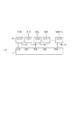
(実施例1)
図1は、実施例1に係る光電変換装置の構成を示すブロック図である。光電変換装置は、画素アレイ1、読み出し部群2、比較部群3、メモリ部群4、参照信号生成部5、カウンタ6、選択部7、同期化部8を含む。
Example 1
FIG. 1 is a block diagram illustrating the configuration of the photoelectric conversion apparatus according to the first embodiment. The photoelectric conversion device includes a
画素アレイ1は、複数列設けられた複数の画素を含む。読み出し部群2は、それぞれが画素アレイ1の各列に対応して設けられた複数の読み出し部を含む。比較部群3は、それぞれが各読み出し部に対応して設けられた複数の比較器を含む。メモリ部群4は、それぞれが各比較器に対応して設けられた複数のメモリ部を含む。参照信号生成部5は、ランプイネーブル信号RAMP_ENの入力に応じて、時間に対して信号レベルが変化する参照信号を出力する。カウンタ6は、カウントイネーブル信号CNT_ENに応じて、第1のクロック信号CLK1をカウントしてMビットのカウント信号を出力する。選択部7は、カウンタ6から出力されたカウント信号およびMビットのデジタルデータ9のいずれかを選択的に同期化部8に出力する。デジタルデータ9は、不図示のデータ供給部から与えられる。同期化部8は、選択部7から出力されたMビットの信号を、第2のクロック信号CLK2に同期した同期化後クロック信号を出力する。各列のメモリ部は対応する比較部の出力が変化すると、それをトリガとして同期化部8の出力を保持する。
The
図2は、画素アレイ1、読み出し部群2、および比較部群3の構成例を1列分だけ示したブロック図である。画素アレイ1には複数の画素21が1個の読み出し部22に共通に接続されている。読み出し部22は例えば定電流源23と増幅器24を含む。定電流源23は、画素21が増幅トランジスタを有する場合に、増幅トランジスタとともにソースフォロワ回路を構成する。増幅器24は、図示したように画素から出力された信号に−A倍のゲインをかける反転増幅回路でも良いし、正のゲインをかける非反転増幅回路でも良く、バッファリングのみを行うバッファ回路であっても良い。読み出し部22は、画素から出力された信号に含まれるノイズ成分を低減するノイズ低減回路をさらに備えても良い。ここでは、増幅器24の出力が、読み出し部22の出力として比較器25に与えられる。
FIG. 2 is a block diagram illustrating a configuration example of the
図3は、図1に示した光電変換装置の動作を説明するためのタイミング図である。説明を簡単にするために、カウンタから出力されるカウント信号の値を10進数で示しているが、実際にはMビットの信号として出力される。また、時刻t1から時刻t3までの期間、選択部7は、カウンタ6から出力されたカウント信号をメモリ部群4に供給するように設定される。
FIG. 3 is a timing chart for explaining the operation of the photoelectric conversion device shown in FIG. In order to simplify the explanation, the value of the count signal output from the counter is shown as a decimal number, but in actuality, it is output as an M-bit signal. In addition, the
時刻t1より前に、デジタル信号に変換されるべきアナログ信号が、比較部群3に、読み出し部群2から与えられているものとする。時刻t1にランプイネーブル信号RAMP_ENおよびカウントイネーブル信号CNT_ENがHレベルになる。これにより、参照信号生成部の出力が時間に対して変化を開始するとともに、カウンタ6が第1のクロック信号CLK1のカウント動作を開始する。本例では、第1のクロック信号CLK1の立ち上がりとともにカウント値がインクリメントする。参照信号は、時間に対してスロープ状に変化するものでもよいし、ステップ状に変化するものであっても良い。
It is assumed that an analog signal to be converted into a digital signal is given from the
時刻t2に読み出し部の出力と参照信号のレベルの大小関係が逆転すると、比較部の出力がHレベルからLレベルに変化し、メモリ部はこの時のカウント信号を保持する。このとき保持されたカウント信号は、読み出し部から出力されたアナログ信号に相当するデジタル信号となる。 When the magnitude relationship between the output of the reading unit and the level of the reference signal is reversed at time t2, the output of the comparison unit changes from the H level to the L level, and the memory unit holds the count signal at this time. The count signal held at this time is a digital signal corresponding to the analog signal output from the reading unit.
その後、時刻t3まで参照信号のレベルが変化し続けてから参照信号の出力がリセットされる。 Thereafter, the reference signal output is reset after the level of the reference signal continues to change until time t3.
変換されるアナログ信号が、AD変換できるダイナミックレンジに入らない場合には、時刻t3までに比較部の出力が変化しない。この場合、当該列のメモリ部には時刻t1よりも前のデータが保持されたままになっているので、異常値となってしまう。そこで、時刻t3の後に、カウント信号に換えてデジタルデータ9をメモリ部に供給するように選択部7を制御して、メモリ部にデジタルデータ9を保持させる。デジタルデータ9は所定の値であり、例えばAD変換できる最大値に対応するデジタル信号である。
When the analog signal to be converted does not fall within the dynamic range in which AD conversion can be performed, the output of the comparison unit does not change until time t3. In this case, since the data before the time t1 is held in the memory portion of the column, an abnormal value is obtained. Therefore, after time t3, the
この後、メモリ部群4に保持されたデジタル信号を、不図示の列選択部により後段の回路へと出力させる。
Thereafter, the digital signal held in the
カウンタ6の構成例として、Gr[0]からGr[M−1]のMビット出力を行うグレイコードカウンタ回路の構成を図4に示す。グレイコードカウンタは、Mビットのバイナリカウンタ回路41とM個の排他的論理和(EXOR)回路42とを含む。バイナリカウンタは第1のクロック信号CLK1の入力を受けてカウント動作を行う。グレイコードカウンタ回路の最上位ビットGr[M−1]を出力するEXOR回路42を除く各EXOR回路42は、バイナリカウンタ回路41の出力のうちの隣接する2個のビットの出力を入力として、1ビットの出力を行う。具体的には、バイナリカウンタの出力B[n]およびB[n+1]を入力としてグレイコードカウンタの出力Gr[n]が生成される(nは自然数)。最上位ビットGr[M−1]を出力するEXOR回路42は、B[M−1]とGNDとに接続される。
As a configuration example of the
最下位ビットGr[0]を例に取って、EXOR回路42の構成を図5に示す。EXOR回路42はインバータ回路部51とスイッチ回路部52とを含む。インバータ回路部51は2個のインバータ回路を含み、B[0]とB[1]とを受けて、これらの反転信号Bb[0]とBb[1]とを出力する。
Taking the least significant bit Gr [0] as an example, the configuration of the
スイッチ回路部52は、4個のスイッチ部SW(T1)〜SW(T4)を含む。スイッチ部SW(T1)は、反転信号Bb[0]で制御されるNMOSトランジスタと反転信号Bb[1]で制御されるNMOSトランジスタが直列に接続されて構成される。スイッチ部SW(T2)は、反転信号Bb[0]で制御されるPMOSトランジスタと信号B[1]で制御されるPMOSトランジスタが直列に接続されて構成される。スイッチ部SW(T3)は、信号B[0]で制御されるPMOSトランジスタと反転信号Bb[1]で制御されるPMOSトランジスタが直列に接続されて構成される。スイッチ部SW(T4)は、信号B[0]で制御されるNMOSトランジスタと信号B[1]で制御されるNMOSトランジスタが直列に接続されて構成される。
The
これらのスイッチ部のうち、スイッチ部SW(T3)とスイッチ部SW(T1)とが直列に接続されており、両者の共通ノードがEXOR回路42の出力ノードGr[0]に接続される。同様に、スイッチ部SW(T2)とスイッチ部SW(T4)とが直列に接続されており、両者の共通ノードがEXOR回路42の出力ノードGr[0]に接続される。
Among these switch units, the switch unit SW (T3) and the switch unit SW (T1) are connected in series, and the common node of both is connected to the output node Gr [0] of the EXOR circuit. Similarly, the switch unit SW (T2) and the switch unit SW (T4) are connected in series, and the common node of both is connected to the output node Gr [0] of the
次に、図6を参照しながらEXOR回路42の動作を説明する。インバータ回路部51の各インバータで生じる遅延をΔtとする。
Next, the operation of the
バイナリカウンタ回路41の出力B[0]およびB[1]は、出力B[0]に対して1/2の周波数で変化する。出力B[0]およびB[1]の状態を踏まえて、T1〜T4の期間に分けて説明する。
The outputs B [0] and B [1] of the
期間T1は、出力B[0]およびB[1]がともにLレベルである。このとき反転信号Bb[0]およびBb[1]はともにHレベルとなりスイッチ部SW(T1)がオンする。これにより、EXOR回路42の出力Gr[0]はLレベルになる。
In the period T1, the outputs B [0] and B [1] are both at the L level. At this time, the inversion signals Bb [0] and Bb [1] are both at the H level, and the switch unit SW (T1) is turned on. As a result, the output Gr [0] of the
期間T2は、出力B[0]がHレベルになり、出力B[1]はLレベルを維持する。出力B[0]の遷移により、その反転信号Bb[0]もLレベルに遷移するが、インバータ回路によるΔtだけ遅れて遷移する。期間T2にはスイッチ部SW(T2)がオンするので、信号B[0]の遷移からΔtだけ遅れてEXOR回路42の出力Gr[0]がHレベルになる。
In the period T2, the output B [0] is at the H level, and the output B [1] is maintained at the L level. Due to the transition of the output B [0], the inverted signal Bb [0] also transitions to the L level, but transitions with a delay of Δt by the inverter circuit. Since the switch section SW (T2) is turned on during the period T2, the output Gr [0] of the
期間T3は、出力B[0]が再びLレベルになり、出力B[1]がHレベルになる。反転信号Bb[0]とBb[1]はともに出力B[0]とB[1]の遷移からΔtだけ遅れて遷移する。期間T3にはスイッチ部SW(T3)がオンするので、EXOR回路42の出力Gr[0]はHレベルを維持する。
In the period T3, the output B [0] becomes the L level again, and the output B [1] becomes the H level. The inversion signals Bb [0] and Bb [1] both transition after a delay of Δt from the transition of the outputs B [0] and B [1]. Since the switch unit SW (T3) is turned on during the period T3, the output Gr [0] of the
期間T4は、出力B[0]がHレベルになり、出力B[1]がHレベルを維持する。反転信号Bb[0]は信号B[0]に対してΔtだけ遅れて遷移する。期間T4にはスイッチ部SW(T4)がオンするので、EXOR回路42の出力Gr[0]はLレベルになる。
In the period T4, the output B [0] is at the H level and the output B [1] is maintained at the H level. The inverted signal Bb [0] transitions with a delay of Δt with respect to the signal B [0]. Since the switch unit SW (T4) is turned on during the period T4, the output Gr [0] of the
以上の説明から理解されるとおり、EXOR回路42の出力Gr[0]は、LレベルからHレベルに遷移するときにΔtだけ遅延し、HレベルからLレベルに遷移するときには遅延が生じない。この結果、出力Gr[0]はHレベルである期間がLレベルである期間よりも短くなり、デューティ比が50%でなくなる。つまり、デューティずれが生じた状態となる。
As understood from the above description, the output Gr [0] of the
4ビットのグレイコードカウンタ回路において、上述したデューティずれが各ビットで発生する場合のタイミング図を図7に示す。 FIG. 7 shows a timing chart when the above-described duty deviation occurs in each bit in the 4-bit Gray code counter circuit.
グレイコードが、あるビットの立ち上がりエッジから別のビットの立ち上がりエッジまでで決定される場合には、正常な期間だけそのコードが維持される。図7においては1および4のグレイコードが該当する。同様に、あるビットの立ち下がりエッジから別のビットの立ち下がりエッジまでで決定される場合にも、正常な期間だけそのコードが維持される。図7においては6のグレイコードが該当する。
If the Gray code is determined from the rising edge of one bit to the rising edge of another bit, the code is maintained for a normal period. In FIG. 7,
しかし、グレイコードがあるビットの立ち下がりエッジから別のビットの立ち上がりエッジまでで決定される場合には、正常な期間よりも長くそのコードが維持される。図7においては0、3、7のグレイコードが該当する。 However, if the Gray code is determined from the falling edge of one bit to the rising edge of another bit, the code is maintained longer than the normal period. In FIG. 7, gray codes of 0, 3, and 7 correspond.
一方、グレイコードがあるビットの立ち上がりエッジから別のビットの立ち下がりエッジまでで決定される場合には、正常な期間よりも短くそのコードが維持される。図7においては2および5のグレイコードが該当する。
On the other hand, when the gray code is determined from the rising edge of one bit to the falling edge of another bit, the code is maintained shorter than the normal period. In FIG. 7,
グレイコードカウンタ回路が各グレイコードを出力する期間の長さが異なる場合には、このグレイコードをカウント信号として用いてAD変換を行うと、変換されるアナログ信号に対して得られるデジタルデータの関係がリニアではなくなる。つまり、AD変換部のリニアリティが低下することになり、ひいては得られる画像の画質が劣化する。 When the gray code counter circuit outputs different gray codes with different lengths, the AD conversion is performed using the gray code as a count signal, and the relationship between the digital data obtained for the converted analog signal Is no longer linear. That is, the linearity of the AD conversion unit is lowered, and consequently the image quality of the obtained image is deteriorated.
そこで、本実施例では、カウンタ6の出力を第2のクロック信号CLK2に同期させて、同期化後クロック信号をメモリ部群4に供給する。
Therefore, in this embodiment, the output of the
図8に同期化部8の構成を示す。同期化部8はM個のフリップフロップ101を含む。各フリップフロップ101は、第2のクロック信号CLK2が共通に与えられるほか、リセット信号RBも共通に与えられる。リセット信号RBがLレベルになるとフリップフロップ101の出力がリセットされる。各フリップフロップ101のD端子には、それぞれグレイコードGi[0:M−1]の各ビットが与えられる。そして、Q端子からは対応するグレイコードを第2のクロック信号CLK2に同期した同期化後クロック信号として、Go[0:M−1]を出力する。
FIG. 8 shows the configuration of the
図9をさらに参照しながら、カウンタ6の出力であるGi[0:M−1]と同期化後クロック信号Go[0:M−1]の関係を説明する。説明を簡単にするために、第1および第2のクロック信号が同位相で同周波数のクロック信号であるとする。
The relationship between Gi [0: M−1], which is the output of the
カウンタ6の出力Gi[0:M−1]は、先述の通り正常な期間の長さよりも長いあるいは短い期間だけ出力されるグレイコードがある。これに対して、カウンタ6の出力Gi[0:M−1]をクロック信号の立ち上がりに同期させると、得られる同期化後カウント信号からは各コードが等しい長さで得られる。この同期化後カウント信号をメモリ部群4に与えることにより、AD変換部のリニアリティが低下することを抑制できる。
As described above, the output Gi [0: M−1] of the
同期化部8は、カウント信号のデューティずれを低減するだけでなく、位相ずれも低減できる。図10は選択部7の1ビット分の構成例を示した回路図である。
The
図10に示した選択部7は、カウント信号が入力される系とデジタルデータが入力される系とを含む。各系に対してNMOSトランジスタ91とPMOSトランジスタ92で構成されたCMOSスイッチが設けられており、2つのCMOSスイッチは、信号SELとその反転信号SELBによって排他的にオンするように構成されている。図1では信号SELおよびSELBは図示を省略した。仮にNMOSトランジスタ91とPMOSトランジスタ92とが、例えば製造時のプロセスばらつきによって異なる駆動力を持つと、選択部7から出力される信号はデューティがずれるおそれがある。さらに、ビット間でもデューティずれの量が異なると、選択部7を経由して出力されたカウント信号はビット間で位相のずれが生じるおそれもある。したがって、図1のように選択部7を備える構成では、選択部7の後段に同期化部8を設けることで、選択部7に起因して生じうるデューティずれや位相ずれも低減することができる。
The
本実施例ではカウンタ6がグレイコードカウンタである場合を詳細に説明したが、例えばバイナリコードカウンタであっても良い。
In the present embodiment, the case where the
バイナリコードカウンタにデューティずれが生じた場合の影響を説明する。図11(A)は3ビットのカウンタにおいて、最下位ビット(1ビット目)にデューティずれが生じて、Hレベルの期間が長い場合のカウント値を示すタイミング図である。2ビット目および3ビット目にはデューティずれが生じておらず、それぞれデューティずれが生じていない場合の最下位ビットの信号に対して1/2倍、1/4倍の周期で遷移するものとする。 The influence when the duty deviation occurs in the binary code counter will be described. FIG. 11A is a timing chart showing a count value when a duty shift occurs in the least significant bit (first bit) and the H level period is long in the 3-bit counter. There is no duty shift in the second bit and the third bit, and each of them transitions at a cycle of 1/2 times and 1/4 times the least significant bit signal when there is no duty shift. To do.
この場合には、2、4、6のカウント値が出力される期間が他のカウント値よりも短くなってしまう。この条件の下、図1に示した光電変換装置に含まれるAD変換部の入出力特性を図11(B)に示す。横軸が変換されるべきアナログ信号で、縦軸がAD変換された後のデジタル信号に対応する。実線で示した理想的な入出力特性に対して、図11(A)に示したデューティずれが生じた場合の入出力特性は破線で示している。破線で示した入出力特性は、理想値からずれているため、AD変換部のリニアリティが低下していることになる。 In this case, the period during which the count values of 2, 4, and 6 are output is shorter than the other count values. FIG. 11B illustrates input / output characteristics of the AD conversion unit included in the photoelectric conversion device illustrated in FIG. 1 under these conditions. The horizontal axis corresponds to an analog signal to be converted, and the vertical axis corresponds to a digital signal after AD conversion. In contrast to the ideal input / output characteristic indicated by the solid line, the input / output characteristic when the duty deviation shown in FIG. Since the input / output characteristics indicated by the broken line are deviated from the ideal values, the linearity of the AD conversion unit is reduced.
上記のように、バイナリコードカウンタをカウンタ6として用いても、同期化部8を設けることにより、デューティずれを低減し、AD変換部のリニアリティが低下することを抑制できる。
As described above, even when the binary code counter is used as the
本実施例では選択部7がデジタルデータ9またはカウンタ6から出力されたカウント信号を選択的に同期化部8に出力する構成を説明したが、選択部7およびデジタルデータ9を省略しても、カウント信号のビット間のデューティずれを低減できる。
In the present embodiment, the configuration in which the
また、本実施例では、第2のクロック信号の立ち上がりエッジに同期して同期化後カウント信号を生成する例を説明したが、立ち下がりエッジを用いても良いし、ビットによって第2のクロック信号のどちらのエッジに同期するかが異なっていてもよい。 In this embodiment, the example in which the count signal after synchronization is generated in synchronization with the rising edge of the second clock signal has been described. However, the falling edge may be used, or the second clock signal may be used depending on the bit. Which edge is synchronized with each other may be different.
また、第1のクロック信号と第2のクロック信号とは異なるものとして説明したが、同一のクロックでも良い。さらに、第1のクロック信号はカウンタを動作させるために用いるため、周波数を過剰に上げるとカウンタが正常に動作しなくなるおそれがある。一方、第2のクロック信号は、カウント信号を同期させるために用いるものなので、第1のクロック信号よりも高い周波数を設定することが容易である。例えば、第2のクロック信号を、第1のクロック信号の2n(nは自然数)倍の周波数を有するクロック信号としても良い。具体的な構成としては、分周器を設けて、第2のクロック信号を1/(2n)に分周したものを第1のクロック信号とすることができる。 Further, although the first clock signal and the second clock signal have been described as being different, the same clock may be used. Furthermore, since the first clock signal is used to operate the counter, if the frequency is increased excessively, the counter may not operate normally. On the other hand, since the second clock signal is used to synchronize the count signal, it is easy to set a frequency higher than that of the first clock signal. For example, the second clock signal may be a clock signal having a frequency 2 n (n is a natural number) times that of the first clock signal. As a specific configuration, a frequency divider is provided, and the first clock signal can be obtained by dividing the second clock signal by 1 / (2 n ).
以上で説明したとおり、本実施例によれば、デューティずれを低減することができる。 As described above, according to this embodiment, the duty deviation can be reduced.
(実施例2)
実施例2を、実施例1との相違点を中心に説明する。
(Example 2)
The second embodiment will be described with a focus on differences from the first embodiment.
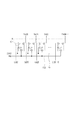
図12は、本実施例に係る光電変換装置の構成を示すブロック図である。図1に示した構成と異なるのは第2の同期化部124を備える点である。本実施例では、第1の同期化部である同期化部8から出力された同期化後カウント信号を、第2の同期化部124がさらに第2のクロック信号CLK2に同期して出力する。
FIG. 12 is a block diagram illustrating a configuration of the photoelectric conversion apparatus according to the present embodiment. The difference from the configuration shown in FIG. 1 is that a
画素アレイの列が増大すると、これに合わせて同期化部8から出力された同期化後カウント信号を伝送する配線も長くなる。これらの配線の寄生抵抗や寄生容量も増大するため、同期化後カウント信号のデューティずれや、各ビット間の位相ずれが生じやすくなる。そこで、本実施例のように構成することで、画素アレイの列が増大しても、同期化後カウント信号のデューティずれを低減することができる。
As the number of columns in the pixel array increases, the length of the wiring for transmitting the post-synchronization count signal output from the
また、同期化後カウント信号を伝送するために、リピートバッファを設けることが考えられる。図13は、同期化部8から出力される同期化後カウント信号の1ビット分を伝送する経路の構成例を示す図である。図のように、リピートバッファとしてリピータ131を伝送系路上に設けて、リピータ131の出力を同期化後カウント信号としてメモリ部群4に供給する。リピータ131は例えば2段のインバータで構成され、インバータを構成するNMOSトランジスタとPMOSトランジスタとの駆動力のばらつきによって各ビットのデューティずれや各ビット間の位相ずれも生じうる。第2の同期化部124を設けることにより、リピータ131に起因するデューティずれや位相のずれを低減できる。
It is also conceivable to provide a repeat buffer in order to transmit the synchronized count signal. FIG. 13 is a diagram illustrating a configuration example of a path for transmitting one bit of the post-synchronization count signal output from the
本実施例では、第2の同期化部124を1個設けた例を示したが、複数の第2の同期化部124を設けても良い。
In the present embodiment, an example in which one
(実施例3)
図14を参照しながら、実施例3に係る光電変換装置を実施例1との相違点を中心に説明する。
(Example 3)
With reference to FIG. 14, the photoelectric conversion device according to the third embodiment will be described focusing on differences from the first embodiment.
本実施例に係る光電変換装置は、メモリ部群4に換えて、デジタル信号生成部群130を備え、カウンタ6に換えてクロック信号生成部131を備える。さらに、本実施例に係る光電変換装置において、第1の同期化部132および第2の同期化部133は、クロック信号生成部131から出力されたクロック信号を第2のクロック信号CLK2に同期させて同期化後クロック信号を出力する。本実施例では、クロック信号生成部131は第1のクロック信号CLK1を受けて、位相の異なる4個のクロック信号を生成する。第1および第2の同期化部132および133は、図8に示したものと同様の構成とすることができる。ただし、カウンタの出力として各フリップフロップに与えられた信号は、クロック信号生成部131から与えられたクロック信号となる点で異なる。
The photoelectric conversion apparatus according to the present embodiment includes a digital signal
図15に、比較部群3とデジタル信号生成部群130のうち、画素アレイの1列に対応する部分を抜き出した図を示す。
FIG. 15 shows a diagram in which a portion corresponding to one column of the pixel array is extracted from the
1個のデジタル信号生成部134はラッチ回路とデコード回路とを含むラッチ&デコード部135と、カウンタ136とを含む。ラッチ&デコード部135は、4個の同期化後クロック信号CLKA〜CLKDおよび比較部の出力を入力信号として受け、比較部の出力が変化したことに応じて、同期化後クロック信号CLKA〜CLKDをラッチ回路がラッチする。ラッチされた同期化後クロック信号は、デコード回路によりデコードされてデコード値として出力される。カウンタ136は、同期化後クロック信号CLKDと比較部の出力を入力信号として受け、同期化後クロック信号CLKD信号に応じてカウント動作を行う。比較部の出力が変化すると、カウンタ136はカウント動作を停止し、その時点でのカウント値を保持する。
One digital
図16は、ラッチ&デコード部135およびカウンタ136の動作例を示すタイミング図である。同期化後クロック信号CLKA〜CLKDは、45度ずつ位相がずれたクロック信号であり、それぞれは、第1のクロック信号CLK1の8周期が1周期となっている。
FIG. 16 is a timing chart showing an operation example of the latch &
カウンタ136は同期化後クロック信号CLKDに応じてカウント動作を行う一方で、ラッチ&デコード部135には同期化後クロック信号CLKA〜CLKDが与えられるため、カウンタ136の1カウントに対してラッチ&デコード部135の出力は8個の状態を取り得る。デジタル信号生成部134がカウンタ136しか持たない場合には、比較器の出力が時刻tAに変化しても、時刻tBに変化しても「0」のカウント値しか得られない。しかし、本例のように構成することで、時刻tAと時刻tBとでラッチ&デコード部135の出力は異なるため、カウント値「0」をさらに高分解能で表現することができる。
While the
以上で説明した本実施例によれば、クロック信号生成部131で生成されたカウント信号を第1の同期化部132で第2のクロック信号に同期させることにより、クロック信号のデューティずれや位相のずれを低減することができる。したがって、光電変換装置の入射光量に対する出力特性のリニアリティが低下することを抑制できる。
According to the present embodiment described above, the count signal generated by the clock
本実施例では、第2の同期化部133を設けて、第1の同期化部132が一部のデジタル信号生成部134に同期化後クロック信号を与え、第2の同期化部133が別の一部のデジタル信号生成部134に同期化後クロック信号を与える構成を示した。しかし、第1の同期化部132から出力されるクロック信号を全てのデジタル信号生成部に与えても良いし、同期化部132の出力を、リピータを介してデジタル信号生成部群130に与えても良い。
In the present embodiment, a
本実施例でも、先の実施例と同じく、第2のクロック信号CLK2の周波数は、第1のクロック信号CLK1の周波数よりも高く設定することができる。第2のクロック信号CLK2が第1のクロック信号CLK1の2n倍の周波数を持っていても良く、分周器を用いてこの関係を実現することも先の実施例と同じである。 Also in this embodiment, the frequency of the second clock signal CLK2 can be set higher than the frequency of the first clock signal CLK1 as in the previous embodiment. The second clock signal CLK2 may have a frequency 2n times that of the first clock signal CLK1, and this relationship is realized by using a frequency divider as in the previous embodiment.
また、各デジタル信号生成部が備えるカウンタは、バイナリコードカウンタでもグレイコードカウンタでも良い。 Further, the counter included in each digital signal generation unit may be a binary code counter or a gray code counter.
(実施例4)
本発明に係る別の実施例を説明する。撮像システムの概略を、図17に示す。
Example 4
Another embodiment according to the present invention will be described. An outline of the imaging system is shown in FIG.
撮像システム1100は、例えば、光学部1110、撮像装置1101、信号処理部1130、記録・通信部1140、タイミング制御回路部1150、システムコントロール回路部1160、および再生・表示部1170を含む。撮像装置1101は、先述の各実施形態で説明した光電変換装置100が用いられる。例えば信号処理部1130は、第2の実施例で説明した、光電変換装置の後段に設けられた回路の機能を有してもよい。
The
レンズなどの光学系である光学部1110は、被写体からの光を撮像装置1101の、複数の画素が2次元状に配列された画素アレイに結像させ、被写体の像を形成する。撮像装置1101は、タイミング制御回路部1150からの信号に基づくタイミングで、画素アレイに結像された光に応じた信号を出力する。
An
撮像装置1101から出力された信号は、映像信号処理部である信号処理部1130に入力され、信号処理部1130が、プログラムなどによって定められた方法に従って、入力された電気信号に対して補正などの処理を行う。信号処理部1130での処理によって得られた信号は画像データとして記録・通信部1140に送られる。記録・通信部1140は、画像を形成するための信号を再生・表示部1170に送り、再生・表示部1170に動画や静止画像が再生・表示させる。記録通信部1140は、また、信号処理部1130からの信号を受けて、システムコントロール回路部1160とも通信を行うほか、不図示の記録媒体に、画像を形成するための信号を記録する動作も行う。
A signal output from the
システムコントロール回路部1160は、撮像システムの動作を統括的に制御するものであり、光学部1110、タイミング制御回路部1150、記録・通信部1140、および再生・表示部1170の駆動を制御する。また、システムコントロール回路部1160は、例えば記録媒体である不図示の記憶装置を備え、ここに撮像システムの動作を制御するのに必要なプログラムなどが記録される。また、システムコントロール回路部1160は、例えばユーザの操作に応じて駆動モードを切り替える信号を撮像システム内で供給する。具体的な例としては、読み出す行やリセットする行の変更、電子ズームに伴う画角の変更や、電子防振に伴う画角のずらしなどである。
The system
タイミング制御回路部1150は、制御部であるシステムコントロール回路部1160による制御に基づいて撮像装置1101および信号処理部1130の駆動タイミングを制御する。
The timing
上述の各実施例は例示的なものであり、本発明の思想を逸脱しない範囲で適宜変更を加えることが可能である。 Each of the above-described embodiments is illustrative, and modifications can be made as appropriate without departing from the spirit of the present invention.
1 画素アレイ
2 読み出し部群
3 比較部群
4 メモリ部群
5 参照信号生成部
6 カウンタ
7 選択部
8 同期化部
124、133 第2の同期化部
130 デジタル信号生成部
131 クロック信号生成部
132 第1の同期化部
DESCRIPTION OF
Claims (16)
各々が前記複数の列のいずれか1つに対応して設けられた複数の比較器と、
前記複数の比較器に参照信号を供給する参照信号生成部と、
グレイコードを構成する複数のビットを含むカウント信号を、第1のクロック信号に同期して生成するカウンタと、
前記カウンタから出力された前記グレイコードを構成する複数のビットを第2のクロック信号に同期化することによって生成された同期化後カウント信号を出力する同期化部と、
各々が前記比較器に対応して設けられ、対応する前記比較器の出力の変化を受けて前記同期化後カウント信号を保持する複数のメモリを有すること
を特徴とする光電変換装置。 A plurality of pixels provided to form a plurality of columns;
A plurality of comparators each provided corresponding to any one of the plurality of columns;
A reference signal generator for supplying a reference signal to the plurality of comparators;
A counter that generates a count signal including a plurality of bits constituting the Gray code in synchronization with the first clock signal;
A synchronization unit for outputting a post-synchronization count signal generated by synchronizing a plurality of bits constituting the Gray code output from the counter with a second clock signal;
A photoelectric conversion device comprising: a plurality of memories, each of which is provided corresponding to the comparator, and holds the post-synchronization count signal in response to a change in the output of the corresponding comparator.
を特徴とする請求項1記載の光電変換装置。 The photoelectric conversion apparatus according to claim 1, wherein the counter includes a binary counter unit that generates a binary code count signal and an EXOR circuit that converts an output of the binary counter unit into a gray code.
各々が前記複数の列のいずれか1つに対応して設けられた複数の比較器と、
前記複数の比較器に参照信号を供給する参照信号生成部と、
複数のビットを含むカウント信号を、第1のクロック信号に同期して生成するカウンタと、
前記複数のビットを第2のクロック信号に同期化することによって生成された同期化後カウント信号を出力する同期化部と、
各々が前記比較器に対応して設けられ、対応する前記比較器の出力の変化を受けて前記同期化後カウント信号を保持する複数のメモリと、
デジタルデータを供給するデータ供給部と、
選択部と、を備え、
前記選択部は、前記デジタルデータと前記カウント信号を選択的に前記同期化部に出力すること
を特徴とする光電変換装置。 A plurality of pixels provided to form a plurality of columns;
A plurality of comparators each provided corresponding to any one of the plurality of columns;
A reference signal generator for supplying a reference signal to the plurality of comparators;
A counter that generates a count signal including a plurality of bits in synchronization with the first clock signal;
A synchronization unit that outputs a post-synchronization count signal generated by synchronizing the plurality of bits with a second clock signal;
A plurality of memories each provided corresponding to the comparator and receiving the change in the output of the corresponding comparator to hold the post-synchronization count signal;
A data supply unit for supplying digital data;
A selection unit, and
The selection unit selectively outputs the digital data and the count signal to the synchronization unit.
前記同期化部から出力された前記同期化後カウント信号を前記複数のメモリのうちの一部に供給し、前記第2の同期化部の出力を前記複数のメモリの別の一部に供給すること
を特徴とする請求項1〜4のいずれかに記載の光電変換装置。 A second synchronization unit that outputs the synchronized count signal output from the synchronization unit in synchronization with the second clock signal;
The post-synchronization count signal output from the synchronization unit is supplied to a part of the plurality of memories, and the output of the second synchronization unit is supplied to another part of the plurality of memories. The photoelectric conversion device according to claim 1, wherein:
前記複数の列に対応して設けられた複数の比較器と、
前記複数の比較器に参照信号を供給する参照信号生成部と、
前記複数の比較器に対応して設けられた複数のデジタル信号生成部と、
互いに位相の異なる複数のクロック信号を生成するクロック信号生成部と、
前記複数のクロック信号を第2のクロック信号に同期化することによって生成された複数の同期化後クロック信号を出力する同期化部と、を備え、
前記複数のデジタル信号生成部の各々は、デコード回路とカウンタとを含み、
前記デコード回路は、前記複数の同期化後クロック信号をデコードして第1のデジタル値に変換し、
前記カウンタは、前記複数の同期化後クロック信号の1つを受けてカウント動作を行うこと
を特徴とする光電変換装置。 A plurality of pixels arranged to form a plurality of columns;
A plurality of comparators provided corresponding to the plurality of columns;
A reference signal generator for supplying a reference signal to the plurality of comparators;
A plurality of digital signal generators provided corresponding to the plurality of comparators;
A clock signal generator for generating a plurality of clock signals having different phases from each other;
A synchronization unit that outputs a plurality of post-synchronization clock signals generated by synchronizing the plurality of clock signals with a second clock signal;
Each of the plurality of digital signal generation units includes a decoding circuit and a counter,
The decoding circuit decodes the plurality of synchronized clock signals and converts them into a first digital value;
The photoelectric conversion apparatus, wherein the counter receives one of the plurality of synchronized clock signals and performs a counting operation.
ことを特徴とする請求項11に記載の光電変換装置。 The digital signal generation unit uses the count value held by the counter as an upper bit when the output of the comparator is inverted, and the first digital signal output by the decode circuit when the output of the comparator is inverted The photoelectric conversion device according to claim 11, wherein a digital signal is generated with a value as a lower bit.
前記同期化部から出力された前記複数の同期化後クロック信号を前記複数のデジタル信号生成部のうちの一部に供給し、前記第2の同期化部から出力された前記複数の第2の同期化後クロック信号を前記複数のデジタル信号生成部の別の一部に供給すること
を特徴とする請求項11または請求項12に記載の光電変換装置。 A second synchronization unit that outputs the plurality of second synchronized clock signals in synchronization with the second clock signal, the plurality of synchronized clock signals output from the synchronization unit;
The plurality of post-synchronization clock signals output from the synchronization unit are supplied to some of the plurality of digital signal generation units, and the plurality of second clocks output from the second synchronization unit The photoelectric conversion device according to claim 11 or 12, wherein the synchronized clock signal is supplied to another part of the plurality of digital signal generation units.
前記複数の画素から成る画素アレイに像を形成する光学系と、
前記光電変換装置から出力された信号を処理して画像データを生成する信号処理部と、をさらに備えたこと
を特徴とする撮像システム。 The photoelectric conversion device according to any one of claims 1 to 15,
An optical system for forming an image on a pixel array comprising a plurality of pixels;
An image pickup system, further comprising: a signal processing unit that processes a signal output from the photoelectric conversion device to generate image data.
Priority Applications (3)
| Application Number | Priority Date | Filing Date | Title |
|---|---|---|---|
| JP2012223307A JP6132506B2 (en) | 2012-10-05 | 2012-10-05 | Photoelectric conversion device and imaging system |
| CN201310446998.3A CN103716553B (en) | 2012-10-05 | 2013-09-26 | Photoelectric conversion device and imaging system |
| US14/043,473 US9467636B2 (en) | 2012-10-05 | 2013-10-01 | Photoelectric conversion device and imaging system |
Applications Claiming Priority (1)
| Application Number | Priority Date | Filing Date | Title |
|---|---|---|---|
| JP2012223307A JP6132506B2 (en) | 2012-10-05 | 2012-10-05 | Photoelectric conversion device and imaging system |
Publications (2)
| Publication Number | Publication Date |
|---|---|
| JP2014075748A JP2014075748A (en) | 2014-04-24 |
| JP6132506B2 true JP6132506B2 (en) | 2017-05-24 |
Family
ID=50409085
Family Applications (1)
| Application Number | Title | Priority Date | Filing Date |
|---|---|---|---|
| JP2012223307A Active JP6132506B2 (en) | 2012-10-05 | 2012-10-05 | Photoelectric conversion device and imaging system |
Country Status (3)
| Country | Link |
|---|---|
| US (1) | US9467636B2 (en) |
| JP (1) | JP6132506B2 (en) |
| CN (1) | CN103716553B (en) |
Families Citing this family (9)
| Publication number | Priority date | Publication date | Assignee | Title |
|---|---|---|---|---|
| JP6049332B2 (en) * | 2012-07-11 | 2016-12-21 | キヤノン株式会社 | Photoelectric conversion device and imaging system |
| KR102292644B1 (en) * | 2013-12-24 | 2021-08-23 | 삼성전자주식회사 | Image sensor for operating with high speed |
| JP6727771B2 (en) * | 2015-08-13 | 2020-07-22 | キヤノン株式会社 | Imaging device |
| CN107436379B (en) * | 2016-05-26 | 2020-08-18 | 中芯国际集成电路制造(上海)有限公司 | System for testing analog signals |
| JP7433741B2 (en) * | 2016-05-31 | 2024-02-20 | キヤノン株式会社 | Photoelectric conversion elements, two-dimensional sensors, image sensors and imaging devices |
| CN105866767A (en) * | 2016-06-12 | 2016-08-17 | 无锡海鹰电子医疗系统有限公司 | Ultrasonic emission channel time-delay control module |
| WO2019033303A1 (en) * | 2017-08-16 | 2019-02-21 | 深圳市汇顶科技股份有限公司 | Image sensing circuit and image depth sensing system |
| US10623728B2 (en) * | 2018-07-06 | 2020-04-14 | Stmicroelectronics (Grenoble 2) Sas | Image sensors for advanced driver assistance systems utilizing safety pixels to detect malfunctions |
| US11356654B2 (en) | 2018-08-01 | 2022-06-07 | Stmicroelectronics Asia Pacific Pte Ltd | Image sensors for advanced driver assistance systems utilizing regulator voltage verification circuitry to detect malfunctions |
Family Cites Families (12)
| Publication number | Priority date | Publication date | Assignee | Title |
|---|---|---|---|---|
| JPH1168553A (en) * | 1997-08-21 | 1999-03-09 | Nec Shizuoka Ltd | Sequencer acceleration circuit |
| JP3714875B2 (en) * | 2001-01-30 | 2005-11-09 | シャープ株式会社 | Gray code counter |
| JP4655500B2 (en) * | 2004-04-12 | 2011-03-23 | ソニー株式会社 | AD converter, semiconductor device for detecting physical quantity distribution, and electronic apparatus |
| JP4289206B2 (en) * | 2004-04-26 | 2009-07-01 | ソニー株式会社 | Counter circuit |
| US7461186B2 (en) * | 2006-02-03 | 2008-12-02 | Infineon Technologies Ag | Data handover unit for transferring data between different clock domains by parallelly reading out data bits from a plurality of storage elements |
| JP4946761B2 (en) * | 2007-09-28 | 2012-06-06 | ソニー株式会社 | Solid-state imaging device and camera system |
| JP4996425B2 (en) * | 2007-11-12 | 2012-08-08 | キヤノン株式会社 | Digital counter, timing generation device, imaging system, and imaging device |
| JP5359521B2 (en) * | 2009-04-24 | 2013-12-04 | ソニー株式会社 | Binary value conversion circuit and method, AD conversion apparatus, solid-state imaging device, and camera system |
| JP5218309B2 (en) * | 2009-07-14 | 2013-06-26 | ソニー株式会社 | Solid-state imaging device, control method therefor, and camera system |
| JP2011166197A (en) | 2010-02-04 | 2011-08-25 | Sony Corp | Signal transmission circuit, column a/d converter, solid-state imaging element, and camera system |
| JP5728826B2 (en) * | 2010-04-30 | 2015-06-03 | ソニー株式会社 | Column A / D converter, column A / D conversion method, solid-state imaging device, and camera system |
| KR20120053555A (en) * | 2010-11-17 | 2012-05-29 | 에스케이하이닉스 주식회사 | Image sensing device |
-
2012
- 2012-10-05 JP JP2012223307A patent/JP6132506B2/en active Active
-
2013
- 2013-09-26 CN CN201310446998.3A patent/CN103716553B/en active Active
- 2013-10-01 US US14/043,473 patent/US9467636B2/en active Active
Also Published As
| Publication number | Publication date |
|---|---|
| CN103716553B (en) | 2017-04-26 |
| US20140098272A1 (en) | 2014-04-10 |
| US9467636B2 (en) | 2016-10-11 |
| JP2014075748A (en) | 2014-04-24 |
| CN103716553A (en) | 2014-04-09 |
Similar Documents
| Publication | Publication Date | Title |
|---|---|---|
| JP6132506B2 (en) | Photoelectric conversion device and imaging system | |
| JP5407523B2 (en) | Integrating AD converter, solid-state imaging device, and camera system | |
| JP4891308B2 (en) | Solid-state imaging device and imaging system using solid-state imaging device | |
| US7859583B2 (en) | Solid-state image capture device, analog/digital conversion method for solid state image capture device, and image capture device | |
| US9204070B2 (en) | Integrating A/D converter, integrating A/D conversion method, solid-state imaging device and camera system | |
| US7088279B2 (en) | AD conversion method, AD converter, semiconductor device for detecting distribution of physical quantities, and electronic apparatus | |
| JP4853445B2 (en) | A / D conversion circuit, solid-state imaging device, and camera system | |
| US9363452B2 (en) | A/D converter, A/D conversion method, solid-state imaging element and camera system | |
| US9019142B2 (en) | Solid-state imaging device, imaging system, and method for driving solid-state imaging device | |
| JP6273126B2 (en) | AD converter, solid-state imaging device, and imaging system | |
| JP2011166197A (en) | Signal transmission circuit, column a/d converter, solid-state imaging element, and camera system | |
| US10129496B2 (en) | Imaging device and imaging system | |
| JP5822547B2 (en) | Imaging apparatus and imaging system | |
| JP2017055382A (en) | Imaging apparatus and imaging system | |
| JP6639271B2 (en) | Imaging device, imaging system | |
| JP5677919B2 (en) | Ramp wave generation circuit and solid-state imaging device | |
| JP2013005089A (en) | Ad conversion circuit and solid state image pickup device | |
| JP6192790B2 (en) | Imaging apparatus and imaging system | |
| JP5425156B2 (en) | AD converter, photoelectric conversion device, and imaging system | |
| JP2014017771A (en) | Photoelectric conversion device and imaging system | |
| JP6022012B2 (en) | Imaging apparatus and imaging system | |
| JP5340373B2 (en) | Solid-state imaging device and imaging system using solid-state imaging device | |
| JP5234157B2 (en) | A / D conversion method and camera system | |
| JP2006108887A (en) | Method for driving solid-state image pickup device |
Legal Events
| Date | Code | Title | Description |
|---|---|---|---|
| A621 | Written request for application examination |
Free format text: JAPANESE INTERMEDIATE CODE: A621 Effective date: 20150831 |
|
| A977 | Report on retrieval |
Free format text: JAPANESE INTERMEDIATE CODE: A971007 Effective date: 20160707 |
|
| A131 | Notification of reasons for refusal |
Free format text: JAPANESE INTERMEDIATE CODE: A131 Effective date: 20160712 |
|
| A521 | Request for written amendment filed |
Free format text: JAPANESE INTERMEDIATE CODE: A523 Effective date: 20160902 |
|
| A131 | Notification of reasons for refusal |
Free format text: JAPANESE INTERMEDIATE CODE: A131 Effective date: 20161206 |
|
| A521 | Request for written amendment filed |
Free format text: JAPANESE INTERMEDIATE CODE: A523 Effective date: 20170130 |
|
| TRDD | Decision of grant or rejection written | ||
| A01 | Written decision to grant a patent or to grant a registration (utility model) |
Free format text: JAPANESE INTERMEDIATE CODE: A01 Effective date: 20170321 |
|
| A61 | First payment of annual fees (during grant procedure) |
Free format text: JAPANESE INTERMEDIATE CODE: A61 Effective date: 20170418 |
|
| R151 | Written notification of patent or utility model registration |
Ref document number: 6132506 Country of ref document: JP Free format text: JAPANESE INTERMEDIATE CODE: R151 |