JP6122985B2 - Semiconductor device - Google Patents
Semiconductor device Download PDFInfo
- Publication number
- JP6122985B2 JP6122985B2 JP2016054137A JP2016054137A JP6122985B2 JP 6122985 B2 JP6122985 B2 JP 6122985B2 JP 2016054137 A JP2016054137 A JP 2016054137A JP 2016054137 A JP2016054137 A JP 2016054137A JP 6122985 B2 JP6122985 B2 JP 6122985B2
- Authority
- JP
- Japan
- Prior art keywords
- wiring
- electrode
- conductive layer
- light
- layer
- Prior art date
- Legal status (The legal status is an assumption and is not a legal conclusion. Google has not performed a legal analysis and makes no representation as to the accuracy of the status listed.)
- Active
Links
- 239000004065 semiconductor Substances 0.000 title claims description 249
- 230000006870 function Effects 0.000 claims description 71
- 239000010410 layer Substances 0.000 description 662
- 239000010408 film Substances 0.000 description 238
- 239000000758 substrate Substances 0.000 description 186
- 239000004973 liquid crystal related substance Substances 0.000 description 150
- 238000000034 method Methods 0.000 description 127
- 239000003990 capacitor Substances 0.000 description 93
- 239000000463 material Substances 0.000 description 85
- 239000010409 thin film Substances 0.000 description 69
- 238000004519 manufacturing process Methods 0.000 description 50
- 238000012937 correction Methods 0.000 description 39
- 238000002834 transmittance Methods 0.000 description 39
- 230000033001 locomotion Effects 0.000 description 29
- 238000003860 storage Methods 0.000 description 29
- 229910052751 metal Inorganic materials 0.000 description 26
- 229910052782 aluminium Inorganic materials 0.000 description 25
- 239000002184 metal Substances 0.000 description 25
- XLOMVQKBTHCTTD-UHFFFAOYSA-N Zinc monoxide Chemical compound [Zn]=O XLOMVQKBTHCTTD-UHFFFAOYSA-N 0.000 description 24
- 238000004544 sputter deposition Methods 0.000 description 24
- XAGFODPZIPBFFR-UHFFFAOYSA-N aluminium Chemical compound [Al] XAGFODPZIPBFFR-UHFFFAOYSA-N 0.000 description 23
- AMGQUBHHOARCQH-UHFFFAOYSA-N indium;oxotin Chemical compound [In].[Sn]=O AMGQUBHHOARCQH-UHFFFAOYSA-N 0.000 description 22
- 239000013078 crystal Substances 0.000 description 21
- 239000011159 matrix material Substances 0.000 description 21
- 239000007769 metal material Substances 0.000 description 21
- PXHVJJICTQNCMI-UHFFFAOYSA-N nickel Substances [Ni] PXHVJJICTQNCMI-UHFFFAOYSA-N 0.000 description 21
- 230000004044 response Effects 0.000 description 20
- VYPSYNLAJGMNEJ-UHFFFAOYSA-N silicon dioxide Inorganic materials O=[Si]=O VYPSYNLAJGMNEJ-UHFFFAOYSA-N 0.000 description 20
- 239000011521 glass Substances 0.000 description 19
- 229910007541 Zn O Inorganic materials 0.000 description 17
- 230000008859 change Effects 0.000 description 16
- 229910052750 molybdenum Inorganic materials 0.000 description 16
- 230000008569 process Effects 0.000 description 16
- 230000001681 protective effect Effects 0.000 description 16
- ZOKXTWBITQBERF-UHFFFAOYSA-N Molybdenum Chemical compound [Mo] ZOKXTWBITQBERF-UHFFFAOYSA-N 0.000 description 15
- XUIMIQQOPSSXEZ-UHFFFAOYSA-N Silicon Chemical compound [Si] XUIMIQQOPSSXEZ-UHFFFAOYSA-N 0.000 description 15
- 230000014759 maintenance of location Effects 0.000 description 15
- 239000011733 molybdenum Substances 0.000 description 15
- 229910052710 silicon Inorganic materials 0.000 description 15
- 239000010703 silicon Substances 0.000 description 15
- 229910052814 silicon oxide Inorganic materials 0.000 description 15
- 239000002356 single layer Substances 0.000 description 15
- 229910052581 Si3N4 Inorganic materials 0.000 description 14
- 230000015572 biosynthetic process Effects 0.000 description 14
- HQVNEWCFYHHQES-UHFFFAOYSA-N silicon nitride Chemical compound N12[Si]34N5[Si]62N3[Si]51N64 HQVNEWCFYHHQES-UHFFFAOYSA-N 0.000 description 14
- 239000013598 vector Substances 0.000 description 14
- 238000010586 diagram Methods 0.000 description 13
- 238000006243 chemical reaction Methods 0.000 description 12
- 238000004891 communication Methods 0.000 description 12
- 239000012535 impurity Substances 0.000 description 12
- 229910003437 indium oxide Inorganic materials 0.000 description 12
- PJXISJQVUVHSOJ-UHFFFAOYSA-N indium(iii) oxide Chemical compound [O-2].[O-2].[O-2].[In+3].[In+3] PJXISJQVUVHSOJ-UHFFFAOYSA-N 0.000 description 12
- 239000002245 particle Substances 0.000 description 12
- BASFCYQUMIYNBI-UHFFFAOYSA-N platinum Chemical compound [Pt] BASFCYQUMIYNBI-UHFFFAOYSA-N 0.000 description 12
- 239000010936 titanium Substances 0.000 description 12
- YVTHLONGBIQYBO-UHFFFAOYSA-N zinc indium(3+) oxygen(2-) Chemical compound [O--].[Zn++].[In+3] YVTHLONGBIQYBO-UHFFFAOYSA-N 0.000 description 12
- 239000011651 chromium Substances 0.000 description 11
- 239000010949 copper Substances 0.000 description 11
- 239000010931 gold Substances 0.000 description 11
- 230000003287 optical effect Effects 0.000 description 11
- 229920005989 resin Polymers 0.000 description 11
- 239000011347 resin Substances 0.000 description 11
- OGIDPMRJRNCKJF-UHFFFAOYSA-N titanium oxide Inorganic materials [Ti]=O OGIDPMRJRNCKJF-UHFFFAOYSA-N 0.000 description 11
- GWEVSGVZZGPLCZ-UHFFFAOYSA-N Titan oxide Chemical compound O=[Ti]=O GWEVSGVZZGPLCZ-UHFFFAOYSA-N 0.000 description 10
- 229910052759 nickel Inorganic materials 0.000 description 10
- 229920003023 plastic Polymers 0.000 description 10
- 239000004033 plastic Substances 0.000 description 10
- 239000011787 zinc oxide Substances 0.000 description 10
- 230000005684 electric field Effects 0.000 description 9
- 238000010438 heat treatment Methods 0.000 description 9
- 239000011572 manganese Substances 0.000 description 9
- 229910052709 silver Inorganic materials 0.000 description 9
- WFKWXMTUELFFGS-UHFFFAOYSA-N tungsten Chemical compound [W] WFKWXMTUELFFGS-UHFFFAOYSA-N 0.000 description 9
- 229910052721 tungsten Inorganic materials 0.000 description 9
- 239000010937 tungsten Substances 0.000 description 9
- BQCADISMDOOEFD-UHFFFAOYSA-N Silver Chemical compound [Ag] BQCADISMDOOEFD-UHFFFAOYSA-N 0.000 description 8
- 206010047571 Visual impairment Diseases 0.000 description 8
- -1 a-InGaZnO Inorganic materials 0.000 description 8
- QVGXLLKOCUKJST-UHFFFAOYSA-N atomic oxygen Chemical compound [O] QVGXLLKOCUKJST-UHFFFAOYSA-N 0.000 description 8
- 229910052804 chromium Inorganic materials 0.000 description 8
- 239000004020 conductor Substances 0.000 description 8
- 229910052738 indium Inorganic materials 0.000 description 8
- 150000004767 nitrides Chemical class 0.000 description 8
- QGLKJKCYBOYXKC-UHFFFAOYSA-N nonaoxidotritungsten Chemical compound O=[W]1(=O)O[W](=O)(=O)O[W](=O)(=O)O1 QGLKJKCYBOYXKC-UHFFFAOYSA-N 0.000 description 8
- 229910052760 oxygen Inorganic materials 0.000 description 8
- 239000001301 oxygen Substances 0.000 description 8
- 239000004332 silver Substances 0.000 description 8
- 239000010935 stainless steel Substances 0.000 description 8
- 229910001220 stainless steel Inorganic materials 0.000 description 8
- 229910052719 titanium Inorganic materials 0.000 description 8
- 229910001930 tungsten oxide Inorganic materials 0.000 description 8
- OKTJSMMVPCPJKN-UHFFFAOYSA-N Carbon Chemical compound [C] OKTJSMMVPCPJKN-UHFFFAOYSA-N 0.000 description 7
- VYZAMTAEIAYCRO-UHFFFAOYSA-N Chromium Chemical compound [Cr] VYZAMTAEIAYCRO-UHFFFAOYSA-N 0.000 description 7
- RYGMFSIKBFXOCR-UHFFFAOYSA-N Copper Chemical compound [Cu] RYGMFSIKBFXOCR-UHFFFAOYSA-N 0.000 description 7
- 229910052779 Neodymium Inorganic materials 0.000 description 7
- RTAQQCXQSZGOHL-UHFFFAOYSA-N Titanium Chemical compound [Ti] RTAQQCXQSZGOHL-UHFFFAOYSA-N 0.000 description 7
- 230000005540 biological transmission Effects 0.000 description 7
- 229910052802 copper Inorganic materials 0.000 description 7
- APFVFJFRJDLVQX-UHFFFAOYSA-N indium atom Chemical compound [In] APFVFJFRJDLVQX-UHFFFAOYSA-N 0.000 description 7
- QEFYFXOXNSNQGX-UHFFFAOYSA-N neodymium atom Chemical compound [Nd] QEFYFXOXNSNQGX-UHFFFAOYSA-N 0.000 description 7
- 239000011368 organic material Substances 0.000 description 7
- 239000000565 sealant Substances 0.000 description 7
- 239000000126 substance Substances 0.000 description 7
- 229910052715 tantalum Inorganic materials 0.000 description 7
- IJGRMHOSHXDMSA-UHFFFAOYSA-N Atomic nitrogen Chemical compound N#N IJGRMHOSHXDMSA-UHFFFAOYSA-N 0.000 description 6
- 229910006404 SnO 2 Inorganic materials 0.000 description 6
- 239000003086 colorant Substances 0.000 description 6
- 150000001875 compounds Chemical class 0.000 description 6
- PMHQVHHXPFUNSP-UHFFFAOYSA-M copper(1+);methylsulfanylmethane;bromide Chemical compound Br[Cu].CSC PMHQVHHXPFUNSP-UHFFFAOYSA-M 0.000 description 6
- 238000002425 crystallisation Methods 0.000 description 6
- 230000008025 crystallization Effects 0.000 description 6
- KPUWHANPEXNPJT-UHFFFAOYSA-N disiloxane Chemical class [SiH3]O[SiH3] KPUWHANPEXNPJT-UHFFFAOYSA-N 0.000 description 6
- 238000001962 electrophoresis Methods 0.000 description 6
- 238000005530 etching Methods 0.000 description 6
- 239000000945 filler Substances 0.000 description 6
- 229910052733 gallium Inorganic materials 0.000 description 6
- 229910052737 gold Inorganic materials 0.000 description 6
- 239000007788 liquid Substances 0.000 description 6
- 238000002844 melting Methods 0.000 description 6
- 230000008018 melting Effects 0.000 description 6
- 239000010955 niobium Substances 0.000 description 6
- 230000002093 peripheral effect Effects 0.000 description 6
- GUVRBAGPIYLISA-UHFFFAOYSA-N tantalum atom Chemical compound [Ta] GUVRBAGPIYLISA-UHFFFAOYSA-N 0.000 description 6
- NIXOWILDQLNWCW-UHFFFAOYSA-N acrylic acid group Chemical group C(C=C)(=O)O NIXOWILDQLNWCW-UHFFFAOYSA-N 0.000 description 5
- 239000000956 alloy Substances 0.000 description 5
- 239000012298 atmosphere Substances 0.000 description 5
- 230000008901 benefit Effects 0.000 description 5
- 229910021393 carbon nanotube Inorganic materials 0.000 description 5
- 239000002041 carbon nanotube Substances 0.000 description 5
- 238000001514 detection method Methods 0.000 description 5
- 230000006866 deterioration Effects 0.000 description 5
- 239000011888 foil Substances 0.000 description 5
- PCHJSUWPFVWCPO-UHFFFAOYSA-N gold Chemical compound [Au] PCHJSUWPFVWCPO-UHFFFAOYSA-N 0.000 description 5
- 229910010272 inorganic material Inorganic materials 0.000 description 5
- 238000003780 insertion Methods 0.000 description 5
- 230000037431 insertion Effects 0.000 description 5
- 229910052748 manganese Inorganic materials 0.000 description 5
- 239000000203 mixture Substances 0.000 description 5
- TWNQGVIAIRXVLR-UHFFFAOYSA-N oxo(oxoalumanyloxy)alumane Chemical compound O=[Al]O[Al]=O TWNQGVIAIRXVLR-UHFFFAOYSA-N 0.000 description 5
- 239000010453 quartz Substances 0.000 description 5
- 239000012798 spherical particle Substances 0.000 description 5
- XOLBLPGZBRYERU-UHFFFAOYSA-N tin dioxide Chemical compound O=[Sn]=O XOLBLPGZBRYERU-UHFFFAOYSA-N 0.000 description 5
- 229910001887 tin oxide Inorganic materials 0.000 description 5
- XKRFYHLGVUSROY-UHFFFAOYSA-N Argon Chemical compound [Ar] XKRFYHLGVUSROY-UHFFFAOYSA-N 0.000 description 4
- 239000004986 Cholesteric liquid crystals (ChLC) Substances 0.000 description 4
- GYHNNYVSQQEPJS-UHFFFAOYSA-N Gallium Chemical compound [Ga] GYHNNYVSQQEPJS-UHFFFAOYSA-N 0.000 description 4
- PWHULOQIROXLJO-UHFFFAOYSA-N Manganese Chemical compound [Mn] PWHULOQIROXLJO-UHFFFAOYSA-N 0.000 description 4
- 239000004642 Polyimide Substances 0.000 description 4
- 229910021417 amorphous silicon Inorganic materials 0.000 description 4
- 238000004380 ashing Methods 0.000 description 4
- 229920001940 conductive polymer Polymers 0.000 description 4
- 238000001816 cooling Methods 0.000 description 4
- 230000003111 delayed effect Effects 0.000 description 4
- 238000005401 electroluminescence Methods 0.000 description 4
- 238000005516 engineering process Methods 0.000 description 4
- 239000007789 gas Substances 0.000 description 4
- 239000001257 hydrogen Substances 0.000 description 4
- 229910052739 hydrogen Inorganic materials 0.000 description 4
- 239000011147 inorganic material Substances 0.000 description 4
- 239000012212 insulator Substances 0.000 description 4
- 230000007246 mechanism Effects 0.000 description 4
- 239000003094 microcapsule Substances 0.000 description 4
- 229910052697 platinum Inorganic materials 0.000 description 4
- 229910021420 polycrystalline silicon Inorganic materials 0.000 description 4
- 229920000728 polyester Polymers 0.000 description 4
- 229920006267 polyester film Polymers 0.000 description 4
- 229920001721 polyimide Polymers 0.000 description 4
- 238000012545 processing Methods 0.000 description 4
- 239000003566 sealing material Substances 0.000 description 4
- 239000011701 zinc Substances 0.000 description 4
- 229910052684 Cerium Inorganic materials 0.000 description 3
- OAICVXFJPJFONN-UHFFFAOYSA-N Phosphorus Chemical compound [P] OAICVXFJPJFONN-UHFFFAOYSA-N 0.000 description 3
- 239000004952 Polyamide Substances 0.000 description 3
- 239000004983 Polymer Dispersed Liquid Crystal Substances 0.000 description 3
- ATJFFYVFTNAWJD-UHFFFAOYSA-N Tin Chemical compound [Sn] ATJFFYVFTNAWJD-UHFFFAOYSA-N 0.000 description 3
- ZWDRUHRMZHJKCZ-UHFFFAOYSA-N [O-2].[Zn+2].[W+2]=O.[O-2] Chemical compound [O-2].[Zn+2].[W+2]=O.[O-2] ZWDRUHRMZHJKCZ-UHFFFAOYSA-N 0.000 description 3
- 230000009471 action Effects 0.000 description 3
- CXKCTMHTOKXKQT-UHFFFAOYSA-N cadmium oxide Inorganic materials [Cd]=O CXKCTMHTOKXKQT-UHFFFAOYSA-N 0.000 description 3
- CFEAAQFZALKQPA-UHFFFAOYSA-N cadmium(2+);oxygen(2-) Chemical compound [O-2].[Cd+2] CFEAAQFZALKQPA-UHFFFAOYSA-N 0.000 description 3
- 230000015556 catabolic process Effects 0.000 description 3
- 239000003054 catalyst Substances 0.000 description 3
- 239000000919 ceramic Substances 0.000 description 3
- GWXLDORMOJMVQZ-UHFFFAOYSA-N cerium Chemical compound [Ce] GWXLDORMOJMVQZ-UHFFFAOYSA-N 0.000 description 3
- 238000011161 development Methods 0.000 description 3
- 230000000694 effects Effects 0.000 description 3
- 230000001747 exhibiting effect Effects 0.000 description 3
- 239000005262 ferroelectric liquid crystals (FLCs) Substances 0.000 description 3
- 230000005669 field effect Effects 0.000 description 3
- 230000006872 improvement Effects 0.000 description 3
- XEEYBQQBJWHFJM-UHFFFAOYSA-N iron Substances [Fe] XEEYBQQBJWHFJM-UHFFFAOYSA-N 0.000 description 3
- 229910044991 metal oxide Inorganic materials 0.000 description 3
- 150000004706 metal oxides Chemical class 0.000 description 3
- 229910021424 microcrystalline silicon Inorganic materials 0.000 description 3
- 229910052758 niobium Inorganic materials 0.000 description 3
- GUCVJGMIXFAOAE-UHFFFAOYSA-N niobium atom Chemical compound [Nb] GUCVJGMIXFAOAE-UHFFFAOYSA-N 0.000 description 3
- 229910052757 nitrogen Inorganic materials 0.000 description 3
- 150000002894 organic compounds Chemical class 0.000 description 3
- 238000005192 partition Methods 0.000 description 3
- 229920002647 polyamide Polymers 0.000 description 3
- 229920002620 polyvinyl fluoride Polymers 0.000 description 3
- 230000009467 reduction Effects 0.000 description 3
- 238000006722 reduction reaction Methods 0.000 description 3
- UWCWUCKPEYNDNV-LBPRGKRZSA-N 2,6-dimethyl-n-[[(2s)-pyrrolidin-2-yl]methyl]aniline Chemical compound CC1=CC=CC(C)=C1NC[C@H]1NCCC1 UWCWUCKPEYNDNV-LBPRGKRZSA-N 0.000 description 2
- JBRZTFJDHDCESZ-UHFFFAOYSA-N AsGa Chemical compound [As]#[Ga] JBRZTFJDHDCESZ-UHFFFAOYSA-N 0.000 description 2
- 238000012935 Averaging Methods 0.000 description 2
- CURLTUGMZLYLDI-UHFFFAOYSA-N Carbon dioxide Chemical compound O=C=O CURLTUGMZLYLDI-UHFFFAOYSA-N 0.000 description 2
- 239000004593 Epoxy Substances 0.000 description 2
- 229910001218 Gallium arsenide Inorganic materials 0.000 description 2
- 239000005264 High molar mass liquid crystal Substances 0.000 description 2
- UFHFLCQGNIYNRP-UHFFFAOYSA-N Hydrogen Chemical compound [H][H] UFHFLCQGNIYNRP-UHFFFAOYSA-N 0.000 description 2
- 239000004988 Nematic liquid crystal Substances 0.000 description 2
- WGLPBDUCMAPZCE-UHFFFAOYSA-N Trioxochromium Chemical compound O=[Cr](=O)=O WGLPBDUCMAPZCE-UHFFFAOYSA-N 0.000 description 2
- 230000001133 acceleration Effects 0.000 description 2
- 238000000137 annealing Methods 0.000 description 2
- 229910052786 argon Inorganic materials 0.000 description 2
- UMIVXZPTRXBADB-UHFFFAOYSA-N benzocyclobutene Chemical compound C1=CC=C2CCC2=C1 UMIVXZPTRXBADB-UHFFFAOYSA-N 0.000 description 2
- 229910052799 carbon Inorganic materials 0.000 description 2
- 229910000423 chromium oxide Inorganic materials 0.000 description 2
- 238000013500 data storage Methods 0.000 description 2
- 238000009792 diffusion process Methods 0.000 description 2
- 230000009977 dual effect Effects 0.000 description 2
- 230000005281 excited state Effects 0.000 description 2
- 239000000284 extract Substances 0.000 description 2
- 230000002349 favourable effect Effects 0.000 description 2
- 239000000835 fiber Substances 0.000 description 2
- 239000011152 fibreglass Substances 0.000 description 2
- 239000012530 fluid Substances 0.000 description 2
- 125000001153 fluoro group Chemical group F* 0.000 description 2
- 230000007274 generation of a signal involved in cell-cell signaling Effects 0.000 description 2
- YBMRDBCBODYGJE-UHFFFAOYSA-N germanium oxide Inorganic materials O=[Ge]=O YBMRDBCBODYGJE-UHFFFAOYSA-N 0.000 description 2
- 238000002347 injection Methods 0.000 description 2
- 239000007924 injection Substances 0.000 description 2
- 229910052742 iron Inorganic materials 0.000 description 2
- 238000001755 magnetron sputter deposition Methods 0.000 description 2
- 229910021421 monocrystalline silicon Inorganic materials 0.000 description 2
- 239000012299 nitrogen atmosphere Substances 0.000 description 2
- 125000000962 organic group Chemical group 0.000 description 2
- PVADDRMAFCOOPC-UHFFFAOYSA-N oxogermanium Chemical compound [Ge]=O PVADDRMAFCOOPC-UHFFFAOYSA-N 0.000 description 2
- 230000000737 periodic effect Effects 0.000 description 2
- 229910052698 phosphorus Inorganic materials 0.000 description 2
- 239000011574 phosphorus Substances 0.000 description 2
- 229920002037 poly(vinyl butyral) polymer Polymers 0.000 description 2
- 229920000139 polyethylene terephthalate Polymers 0.000 description 2
- 239000005020 polyethylene terephthalate Substances 0.000 description 2
- 239000004800 polyvinyl chloride Substances 0.000 description 2
- 229920000915 polyvinyl chloride Polymers 0.000 description 2
- 239000000843 powder Substances 0.000 description 2
- 238000001552 radio frequency sputter deposition Methods 0.000 description 2
- 125000006850 spacer group Chemical group 0.000 description 2
- 230000007704 transition Effects 0.000 description 2
- 229910052723 transition metal Inorganic materials 0.000 description 2
- 210000003462 vein Anatomy 0.000 description 2
- XLYOFNOQVPJJNP-UHFFFAOYSA-N water Substances O XLYOFNOQVPJJNP-UHFFFAOYSA-N 0.000 description 2
- QTBSBXVTEAMEQO-UHFFFAOYSA-M Acetate Chemical compound CC([O-])=O QTBSBXVTEAMEQO-UHFFFAOYSA-M 0.000 description 1
- 239000004925 Acrylic resin Substances 0.000 description 1
- 229920000178 Acrylic resin Polymers 0.000 description 1
- 229910017073 AlLi Inorganic materials 0.000 description 1
- ZOXJGFHDIHLPTG-UHFFFAOYSA-N Boron Chemical compound [B] ZOXJGFHDIHLPTG-UHFFFAOYSA-N 0.000 description 1
- 244000025254 Cannabis sativa Species 0.000 description 1
- 235000012766 Cannabis sativa ssp. sativa var. sativa Nutrition 0.000 description 1
- 235000012765 Cannabis sativa ssp. sativa var. spontanea Nutrition 0.000 description 1
- 229920000298 Cellophane Polymers 0.000 description 1
- 229920000742 Cotton Polymers 0.000 description 1
- 229910019974 CrSi Inorganic materials 0.000 description 1
- 239000004985 Discotic Liquid Crystal Substance Substances 0.000 description 1
- 206010052128 Glare Diseases 0.000 description 1
- 241000282412 Homo Species 0.000 description 1
- DGAQECJNVWCQMB-PUAWFVPOSA-M Ilexoside XXIX Chemical compound C[C@@H]1CC[C@@]2(CC[C@@]3(C(=CC[C@H]4[C@]3(CC[C@@H]5[C@@]4(CC[C@@H](C5(C)C)OS(=O)(=O)[O-])C)C)[C@@H]2[C@]1(C)O)C)C(=O)O[C@H]6[C@@H]([C@H]([C@@H]([C@H](O6)CO)O)O)O.[Na+] DGAQECJNVWCQMB-PUAWFVPOSA-M 0.000 description 1
- GPXJNWSHGFTCBW-UHFFFAOYSA-N Indium phosphide Chemical compound [In]#P GPXJNWSHGFTCBW-UHFFFAOYSA-N 0.000 description 1
- 239000004976 Lyotropic liquid crystal Substances 0.000 description 1
- 241001465754 Metazoa Species 0.000 description 1
- 229910016006 MoSi Inorganic materials 0.000 description 1
- 240000008790 Musa x paradisiaca Species 0.000 description 1
- 235000018290 Musa x paradisiaca Nutrition 0.000 description 1
- 239000004677 Nylon Substances 0.000 description 1
- 229920012266 Poly(ether sulfone) PES Polymers 0.000 description 1
- 229920001665 Poly-4-vinylphenol Polymers 0.000 description 1
- 239000004743 Polypropylene Substances 0.000 description 1
- 229920000297 Rayon Polymers 0.000 description 1
- 229910000577 Silicon-germanium Inorganic materials 0.000 description 1
- 239000004990 Smectic liquid crystal Substances 0.000 description 1
- 229910020923 Sn-O Inorganic materials 0.000 description 1
- 101100268330 Solanum lycopersicum TFT7 gene Proteins 0.000 description 1
- 239000004974 Thermotropic liquid crystal Substances 0.000 description 1
- 208000003443 Unconsciousness Diseases 0.000 description 1
- BZHJMEDXRYGGRV-UHFFFAOYSA-N Vinyl chloride Chemical compound ClC=C BZHJMEDXRYGGRV-UHFFFAOYSA-N 0.000 description 1
- GDFCWFBWQUEQIJ-UHFFFAOYSA-N [B].[P] Chemical compound [B].[P] GDFCWFBWQUEQIJ-UHFFFAOYSA-N 0.000 description 1
- 238000009825 accumulation Methods 0.000 description 1
- 239000002253 acid Substances 0.000 description 1
- 230000002776 aggregation Effects 0.000 description 1
- 238000004220 aggregation Methods 0.000 description 1
- 125000000217 alkyl group Chemical group 0.000 description 1
- 229910045601 alloy Inorganic materials 0.000 description 1
- 239000005407 aluminoborosilicate glass Substances 0.000 description 1
- 238000013459 approach Methods 0.000 description 1
- 239000012300 argon atmosphere Substances 0.000 description 1
- 238000000149 argon plasma sintering Methods 0.000 description 1
- 229910052785 arsenic Inorganic materials 0.000 description 1
- RQNWIZPPADIBDY-UHFFFAOYSA-N arsenic atom Chemical compound [As] RQNWIZPPADIBDY-UHFFFAOYSA-N 0.000 description 1
- 125000003118 aryl group Chemical group 0.000 description 1
- 229910052788 barium Inorganic materials 0.000 description 1
- DSAJWYNOEDNPEQ-UHFFFAOYSA-N barium atom Chemical compound [Ba] DSAJWYNOEDNPEQ-UHFFFAOYSA-N 0.000 description 1
- 239000011230 binding agent Substances 0.000 description 1
- 229910052796 boron Inorganic materials 0.000 description 1
- 239000005380 borophosphosilicate glass Substances 0.000 description 1
- 239000005388 borosilicate glass Substances 0.000 description 1
- NNBFNNNWANBMTI-UHFFFAOYSA-M brilliant green Chemical compound OS([O-])(=O)=O.C1=CC(N(CC)CC)=CC=C1C(C=1C=CC=CC=1)=C1C=CC(=[N+](CC)CC)C=C1 NNBFNNNWANBMTI-UHFFFAOYSA-M 0.000 description 1
- DQXBYHZEEUGOBF-UHFFFAOYSA-N but-3-enoic acid;ethene Chemical compound C=C.OC(=O)CC=C DQXBYHZEEUGOBF-UHFFFAOYSA-N 0.000 description 1
- IEJHYFOJNUCIBD-UHFFFAOYSA-N cadmium(2+) indium(3+) oxygen(2-) Chemical compound [O-2].[Cd+2].[In+3] IEJHYFOJNUCIBD-UHFFFAOYSA-N 0.000 description 1
- BEQNOZDXPONEMR-UHFFFAOYSA-N cadmium;oxotin Chemical compound [Cd].[Sn]=O BEQNOZDXPONEMR-UHFFFAOYSA-N 0.000 description 1
- 235000009120 camo Nutrition 0.000 description 1
- 229910002092 carbon dioxide Inorganic materials 0.000 description 1
- 239000001569 carbon dioxide Substances 0.000 description 1
- 239000000969 carrier Substances 0.000 description 1
- 230000001413 cellular effect Effects 0.000 description 1
- 235000005607 chanvre indien Nutrition 0.000 description 1
- 238000005229 chemical vapour deposition Methods 0.000 description 1
- 230000003098 cholesteric effect Effects 0.000 description 1
- 238000004040 coloring Methods 0.000 description 1
- 239000000306 component Substances 0.000 description 1
- 239000000356 contaminant Substances 0.000 description 1
- 229920001577 copolymer Polymers 0.000 description 1
- 238000007872 degassing Methods 0.000 description 1
- 238000006731 degradation reaction Methods 0.000 description 1
- 210000004207 dermis Anatomy 0.000 description 1
- 238000013461 design Methods 0.000 description 1
- 239000010432 diamond Substances 0.000 description 1
- 229910003460 diamond Inorganic materials 0.000 description 1
- 239000003989 dielectric material Substances 0.000 description 1
- 208000037265 diseases, disorders, signs and symptoms Diseases 0.000 description 1
- 239000006185 dispersion Substances 0.000 description 1
- 238000006073 displacement reaction Methods 0.000 description 1
- 229920001971 elastomer Polymers 0.000 description 1
- 238000004070 electrodeposition Methods 0.000 description 1
- 210000002615 epidermis Anatomy 0.000 description 1
- 239000003822 epoxy resin Substances 0.000 description 1
- 239000005038 ethylene vinyl acetate Substances 0.000 description 1
- 239000004744 fabric Substances 0.000 description 1
- 239000002657 fibrous material Substances 0.000 description 1
- 238000007667 floating Methods 0.000 description 1
- 230000005283 ground state Effects 0.000 description 1
- 239000011487 hemp Substances 0.000 description 1
- 238000000097 high energy electron diffraction Methods 0.000 description 1
- 230000005525 hole transport Effects 0.000 description 1
- 150000002431 hydrogen Chemical class 0.000 description 1
- 239000011261 inert gas Substances 0.000 description 1
- 150000002484 inorganic compounds Chemical class 0.000 description 1
- 239000011810 insulating material Substances 0.000 description 1
- 230000010354 integration Effects 0.000 description 1
- 239000011229 interlayer Substances 0.000 description 1
- 150000002500 ions Chemical class 0.000 description 1
- 230000001678 irradiating effect Effects 0.000 description 1
- 238000003475 lamination Methods 0.000 description 1
- 239000010985 leather Substances 0.000 description 1
- 230000031700 light absorption Effects 0.000 description 1
- 238000004020 luminiscence type Methods 0.000 description 1
- 230000005389 magnetism Effects 0.000 description 1
- QSHDDOUJBYECFT-UHFFFAOYSA-N mercury Chemical compound [Hg] QSHDDOUJBYECFT-UHFFFAOYSA-N 0.000 description 1
- 229910052753 mercury Inorganic materials 0.000 description 1
- 229910021645 metal ion Inorganic materials 0.000 description 1
- 150000002739 metals Chemical class 0.000 description 1
- 239000013081 microcrystal Substances 0.000 description 1
- 238000012986 modification Methods 0.000 description 1
- 230000004048 modification Effects 0.000 description 1
- 239000002159 nanocrystal Substances 0.000 description 1
- 229920001778 nylon Polymers 0.000 description 1
- 238000007645 offset printing Methods 0.000 description 1
- 239000012788 optical film Substances 0.000 description 1
- AHLBNYSZXLDEJQ-FWEHEUNISA-N orlistat Chemical compound CCCCCCCCCCC[C@H](OC(=O)[C@H](CC(C)C)NC=O)C[C@@H]1OC(=O)[C@H]1CCCCCC AHLBNYSZXLDEJQ-FWEHEUNISA-N 0.000 description 1
- KYKLWYKWCAYAJY-UHFFFAOYSA-N oxotin;zinc Chemical compound [Zn].[Sn]=O KYKLWYKWCAYAJY-UHFFFAOYSA-N 0.000 description 1
- BPUBBGLMJRNUCC-UHFFFAOYSA-N oxygen(2-);tantalum(5+) Chemical compound [O-2].[O-2].[O-2].[O-2].[O-2].[Ta+5].[Ta+5] BPUBBGLMJRNUCC-UHFFFAOYSA-N 0.000 description 1
- 206010033675 panniculitis Diseases 0.000 description 1
- 230000003071 parasitic effect Effects 0.000 description 1
- 238000000059 patterning Methods 0.000 description 1
- 239000000049 pigment Substances 0.000 description 1
- 229920001200 poly(ethylene-vinyl acetate) Polymers 0.000 description 1
- 229920000767 polyaniline Polymers 0.000 description 1
- 229920000647 polyepoxide Polymers 0.000 description 1
- 239000011112 polyethylene naphthalate Substances 0.000 description 1
- 229920000642 polymer Polymers 0.000 description 1
- 229920001155 polypropylene Polymers 0.000 description 1
- 229920000128 polypyrrole Polymers 0.000 description 1
- 229920001296 polysiloxane Polymers 0.000 description 1
- 229920000123 polythiophene Polymers 0.000 description 1
- 229920002635 polyurethane Polymers 0.000 description 1
- 239000004814 polyurethane Substances 0.000 description 1
- 229910021426 porous silicon Inorganic materials 0.000 description 1
- 238000001556 precipitation Methods 0.000 description 1
- 238000007639 printing Methods 0.000 description 1
- 230000005855 radiation Effects 0.000 description 1
- 239000002964 rayon Substances 0.000 description 1
- 238000005546 reactive sputtering Methods 0.000 description 1
- 230000008707 rearrangement Effects 0.000 description 1
- 230000006798 recombination Effects 0.000 description 1
- 238000005215 recombination Methods 0.000 description 1
- 238000002310 reflectometry Methods 0.000 description 1
- 230000003252 repetitive effect Effects 0.000 description 1
- 239000005060 rubber Substances 0.000 description 1
- 229910052594 sapphire Inorganic materials 0.000 description 1
- 239000010980 sapphire Substances 0.000 description 1
- 238000007650 screen-printing Methods 0.000 description 1
- 238000007789 sealing Methods 0.000 description 1
- 238000004904 shortening Methods 0.000 description 1
- 229920002050 silicone resin Polymers 0.000 description 1
- 239000010944 silver (metal) Substances 0.000 description 1
- 210000003491 skin Anatomy 0.000 description 1
- 229910052708 sodium Inorganic materials 0.000 description 1
- 239000011734 sodium Substances 0.000 description 1
- 239000007787 solid Substances 0.000 description 1
- 239000000243 solution Substances 0.000 description 1
- 238000004528 spin coating Methods 0.000 description 1
- 238000005507 spraying Methods 0.000 description 1
- 239000007858 starting material Substances 0.000 description 1
- 239000004575 stone Substances 0.000 description 1
- 230000035882 stress Effects 0.000 description 1
- 210000004304 subcutaneous tissue Anatomy 0.000 description 1
- 125000001424 substituent group Chemical group 0.000 description 1
- 229920002994 synthetic fiber Polymers 0.000 description 1
- 239000012209 synthetic fiber Substances 0.000 description 1
- 229920003002 synthetic resin Polymers 0.000 description 1
- 239000000057 synthetic resin Substances 0.000 description 1
- 229910001936 tantalum oxide Inorganic materials 0.000 description 1
- 239000013077 target material Substances 0.000 description 1
- 230000002123 temporal effect Effects 0.000 description 1
- 230000008646 thermal stress Effects 0.000 description 1
- 229920001187 thermosetting polymer Polymers 0.000 description 1
- 229910000314 transition metal oxide Inorganic materials 0.000 description 1
- 150000003624 transition metals Chemical class 0.000 description 1
- 238000007740 vapor deposition Methods 0.000 description 1
- 125000000391 vinyl group Chemical group [H]C([*])=C([H])[H] 0.000 description 1
- 229920002554 vinyl polymer Polymers 0.000 description 1
- 239000002023 wood Substances 0.000 description 1
- 229910052725 zinc Inorganic materials 0.000 description 1
- TYHJXGDMRRJCRY-UHFFFAOYSA-N zinc indium(3+) oxygen(2-) tin(4+) Chemical compound [O-2].[Zn+2].[Sn+4].[In+3] TYHJXGDMRRJCRY-UHFFFAOYSA-N 0.000 description 1
Images


Classifications
-
- H—ELECTRICITY
- H01—ELECTRIC ELEMENTS
- H01L—SEMICONDUCTOR DEVICES NOT COVERED BY CLASS H10
- H01L29/00—Semiconductor devices adapted for rectifying, amplifying, oscillating or switching, or capacitors or resistors with at least one potential-jump barrier or surface barrier, e.g. PN junction depletion layer or carrier concentration layer; Details of semiconductor bodies or of electrodes thereof ; Multistep manufacturing processes therefor
- H01L29/40—Electrodes ; Multistep manufacturing processes therefor
- H01L29/43—Electrodes ; Multistep manufacturing processes therefor characterised by the materials of which they are formed
- H01L29/49—Metal-insulator-semiconductor electrodes, e.g. gates of MOSFET
- H01L29/4908—Metal-insulator-semiconductor electrodes, e.g. gates of MOSFET for thin film semiconductor, e.g. gate of TFT
-
- H—ELECTRICITY
- H01—ELECTRIC ELEMENTS
- H01L—SEMICONDUCTOR DEVICES NOT COVERED BY CLASS H10
- H01L27/00—Devices consisting of a plurality of semiconductor or other solid-state components formed in or on a common substrate
- H01L27/02—Devices consisting of a plurality of semiconductor or other solid-state components formed in or on a common substrate including semiconductor components specially adapted for rectifying, oscillating, amplifying or switching and having at least one potential-jump barrier or surface barrier; including integrated passive circuit elements with at least one potential-jump barrier or surface barrier
- H01L27/12—Devices consisting of a plurality of semiconductor or other solid-state components formed in or on a common substrate including semiconductor components specially adapted for rectifying, oscillating, amplifying or switching and having at least one potential-jump barrier or surface barrier; including integrated passive circuit elements with at least one potential-jump barrier or surface barrier the substrate being other than a semiconductor body, e.g. an insulating body
- H01L27/1214—Devices consisting of a plurality of semiconductor or other solid-state components formed in or on a common substrate including semiconductor components specially adapted for rectifying, oscillating, amplifying or switching and having at least one potential-jump barrier or surface barrier; including integrated passive circuit elements with at least one potential-jump barrier or surface barrier the substrate being other than a semiconductor body, e.g. an insulating body comprising a plurality of TFTs formed on a non-semiconducting substrate, e.g. driving circuits for AMLCDs
- H01L27/1222—Devices consisting of a plurality of semiconductor or other solid-state components formed in or on a common substrate including semiconductor components specially adapted for rectifying, oscillating, amplifying or switching and having at least one potential-jump barrier or surface barrier; including integrated passive circuit elements with at least one potential-jump barrier or surface barrier the substrate being other than a semiconductor body, e.g. an insulating body comprising a plurality of TFTs formed on a non-semiconducting substrate, e.g. driving circuits for AMLCDs with a particular composition, shape or crystalline structure of the active layer
- H01L27/1225—Devices consisting of a plurality of semiconductor or other solid-state components formed in or on a common substrate including semiconductor components specially adapted for rectifying, oscillating, amplifying or switching and having at least one potential-jump barrier or surface barrier; including integrated passive circuit elements with at least one potential-jump barrier or surface barrier the substrate being other than a semiconductor body, e.g. an insulating body comprising a plurality of TFTs formed on a non-semiconducting substrate, e.g. driving circuits for AMLCDs with a particular composition, shape or crystalline structure of the active layer with semiconductor materials not belonging to the group IV of the periodic table, e.g. InGaZnO
-
- H—ELECTRICITY
- H01—ELECTRIC ELEMENTS
- H01L—SEMICONDUCTOR DEVICES NOT COVERED BY CLASS H10
- H01L27/00—Devices consisting of a plurality of semiconductor or other solid-state components formed in or on a common substrate
- H01L27/02—Devices consisting of a plurality of semiconductor or other solid-state components formed in or on a common substrate including semiconductor components specially adapted for rectifying, oscillating, amplifying or switching and having at least one potential-jump barrier or surface barrier; including integrated passive circuit elements with at least one potential-jump barrier or surface barrier
- H01L27/12—Devices consisting of a plurality of semiconductor or other solid-state components formed in or on a common substrate including semiconductor components specially adapted for rectifying, oscillating, amplifying or switching and having at least one potential-jump barrier or surface barrier; including integrated passive circuit elements with at least one potential-jump barrier or surface barrier the substrate being other than a semiconductor body, e.g. an insulating body
- H01L27/1214—Devices consisting of a plurality of semiconductor or other solid-state components formed in or on a common substrate including semiconductor components specially adapted for rectifying, oscillating, amplifying or switching and having at least one potential-jump barrier or surface barrier; including integrated passive circuit elements with at least one potential-jump barrier or surface barrier the substrate being other than a semiconductor body, e.g. an insulating body comprising a plurality of TFTs formed on a non-semiconducting substrate, e.g. driving circuits for AMLCDs
- H01L27/124—Devices consisting of a plurality of semiconductor or other solid-state components formed in or on a common substrate including semiconductor components specially adapted for rectifying, oscillating, amplifying or switching and having at least one potential-jump barrier or surface barrier; including integrated passive circuit elements with at least one potential-jump barrier or surface barrier the substrate being other than a semiconductor body, e.g. an insulating body comprising a plurality of TFTs formed on a non-semiconducting substrate, e.g. driving circuits for AMLCDs with a particular composition, shape or layout of the wiring layers specially adapted to the circuit arrangement, e.g. scanning lines in LCD pixel circuits
-
- H—ELECTRICITY
- H01—ELECTRIC ELEMENTS
- H01L—SEMICONDUCTOR DEVICES NOT COVERED BY CLASS H10
- H01L27/00—Devices consisting of a plurality of semiconductor or other solid-state components formed in or on a common substrate
- H01L27/02—Devices consisting of a plurality of semiconductor or other solid-state components formed in or on a common substrate including semiconductor components specially adapted for rectifying, oscillating, amplifying or switching and having at least one potential-jump barrier or surface barrier; including integrated passive circuit elements with at least one potential-jump barrier or surface barrier
- H01L27/12—Devices consisting of a plurality of semiconductor or other solid-state components formed in or on a common substrate including semiconductor components specially adapted for rectifying, oscillating, amplifying or switching and having at least one potential-jump barrier or surface barrier; including integrated passive circuit elements with at least one potential-jump barrier or surface barrier the substrate being other than a semiconductor body, e.g. an insulating body
- H01L27/1214—Devices consisting of a plurality of semiconductor or other solid-state components formed in or on a common substrate including semiconductor components specially adapted for rectifying, oscillating, amplifying or switching and having at least one potential-jump barrier or surface barrier; including integrated passive circuit elements with at least one potential-jump barrier or surface barrier the substrate being other than a semiconductor body, e.g. an insulating body comprising a plurality of TFTs formed on a non-semiconducting substrate, e.g. driving circuits for AMLCDs
- H01L27/1248—Devices consisting of a plurality of semiconductor or other solid-state components formed in or on a common substrate including semiconductor components specially adapted for rectifying, oscillating, amplifying or switching and having at least one potential-jump barrier or surface barrier; including integrated passive circuit elements with at least one potential-jump barrier or surface barrier the substrate being other than a semiconductor body, e.g. an insulating body comprising a plurality of TFTs formed on a non-semiconducting substrate, e.g. driving circuits for AMLCDs with a particular composition or shape of the interlayer dielectric specially adapted to the circuit arrangement
-
- H—ELECTRICITY
- H01—ELECTRIC ELEMENTS
- H01L—SEMICONDUCTOR DEVICES NOT COVERED BY CLASS H10
- H01L27/00—Devices consisting of a plurality of semiconductor or other solid-state components formed in or on a common substrate
- H01L27/02—Devices consisting of a plurality of semiconductor or other solid-state components formed in or on a common substrate including semiconductor components specially adapted for rectifying, oscillating, amplifying or switching and having at least one potential-jump barrier or surface barrier; including integrated passive circuit elements with at least one potential-jump barrier or surface barrier
- H01L27/12—Devices consisting of a plurality of semiconductor or other solid-state components formed in or on a common substrate including semiconductor components specially adapted for rectifying, oscillating, amplifying or switching and having at least one potential-jump barrier or surface barrier; including integrated passive circuit elements with at least one potential-jump barrier or surface barrier the substrate being other than a semiconductor body, e.g. an insulating body
- H01L27/1214—Devices consisting of a plurality of semiconductor or other solid-state components formed in or on a common substrate including semiconductor components specially adapted for rectifying, oscillating, amplifying or switching and having at least one potential-jump barrier or surface barrier; including integrated passive circuit elements with at least one potential-jump barrier or surface barrier the substrate being other than a semiconductor body, e.g. an insulating body comprising a plurality of TFTs formed on a non-semiconducting substrate, e.g. driving circuits for AMLCDs
- H01L27/1259—Multistep manufacturing methods
- H01L27/1288—Multistep manufacturing methods employing particular masking sequences or specially adapted masks, e.g. half-tone mask
-
- H—ELECTRICITY
- H01—ELECTRIC ELEMENTS
- H01L—SEMICONDUCTOR DEVICES NOT COVERED BY CLASS H10
- H01L29/00—Semiconductor devices adapted for rectifying, amplifying, oscillating or switching, or capacitors or resistors with at least one potential-jump barrier or surface barrier, e.g. PN junction depletion layer or carrier concentration layer; Details of semiconductor bodies or of electrodes thereof ; Multistep manufacturing processes therefor
- H01L29/40—Electrodes ; Multistep manufacturing processes therefor
- H01L29/43—Electrodes ; Multistep manufacturing processes therefor characterised by the materials of which they are formed
- H01L29/45—Ohmic electrodes
- H01L29/456—Ohmic electrodes on silicon
- H01L29/458—Ohmic electrodes on silicon for thin film silicon, e.g. source or drain electrode
-
- H—ELECTRICITY
- H01—ELECTRIC ELEMENTS
- H01L—SEMICONDUCTOR DEVICES NOT COVERED BY CLASS H10
- H01L29/00—Semiconductor devices adapted for rectifying, amplifying, oscillating or switching, or capacitors or resistors with at least one potential-jump barrier or surface barrier, e.g. PN junction depletion layer or carrier concentration layer; Details of semiconductor bodies or of electrodes thereof ; Multistep manufacturing processes therefor
- H01L29/66—Types of semiconductor device ; Multistep manufacturing processes therefor
- H01L29/68—Types of semiconductor device ; Multistep manufacturing processes therefor controllable by only the electric current supplied, or only the electric potential applied, to an electrode which does not carry the current to be rectified, amplified or switched
- H01L29/76—Unipolar devices, e.g. field effect transistors
- H01L29/772—Field effect transistors
- H01L29/78—Field effect transistors with field effect produced by an insulated gate
- H01L29/786—Thin film transistors, i.e. transistors with a channel being at least partly a thin film
- H01L29/7869—Thin film transistors, i.e. transistors with a channel being at least partly a thin film having a semiconductor body comprising an oxide semiconductor material, e.g. zinc oxide, copper aluminium oxide, cadmium stannate
-
- H—ELECTRICITY
- H10—SEMICONDUCTOR DEVICES; ELECTRIC SOLID-STATE DEVICES NOT OTHERWISE PROVIDED FOR
- H10K—ORGANIC ELECTRIC SOLID-STATE DEVICES
- H10K50/00—Organic light-emitting devices
- H10K50/10—OLEDs or polymer light-emitting diodes [PLED]
- H10K50/11—OLEDs or polymer light-emitting diodes [PLED] characterised by the electroluminescent [EL] layers
-
- H—ELECTRICITY
- H10—SEMICONDUCTOR DEVICES; ELECTRIC SOLID-STATE DEVICES NOT OTHERWISE PROVIDED FOR
- H10K—ORGANIC ELECTRIC SOLID-STATE DEVICES
- H10K50/00—Organic light-emitting devices
- H10K50/80—Constructional details
- H10K50/805—Electrodes
-
- H—ELECTRICITY
- H10—SEMICONDUCTOR DEVICES; ELECTRIC SOLID-STATE DEVICES NOT OTHERWISE PROVIDED FOR
- H10K—ORGANIC ELECTRIC SOLID-STATE DEVICES
- H10K59/00—Integrated devices, or assemblies of multiple devices, comprising at least one organic light-emitting element covered by group H10K50/00
- H10K59/10—OLED displays
- H10K59/12—Active-matrix OLED [AMOLED] displays
- H10K59/121—Active-matrix OLED [AMOLED] displays characterised by the geometry or disposition of pixel elements
- H10K59/1213—Active-matrix OLED [AMOLED] displays characterised by the geometry or disposition of pixel elements the pixel elements being TFTs
-
- H—ELECTRICITY
- H10—SEMICONDUCTOR DEVICES; ELECTRIC SOLID-STATE DEVICES NOT OTHERWISE PROVIDED FOR
- H10K—ORGANIC ELECTRIC SOLID-STATE DEVICES
- H10K59/00—Integrated devices, or assemblies of multiple devices, comprising at least one organic light-emitting element covered by group H10K50/00
- H10K59/10—OLED displays
- H10K59/12—Active-matrix OLED [AMOLED] displays
- H10K59/123—Connection of the pixel electrodes to the thin film transistors [TFT]
-
- H—ELECTRICITY
- H10—SEMICONDUCTOR DEVICES; ELECTRIC SOLID-STATE DEVICES NOT OTHERWISE PROVIDED FOR
- H10K—ORGANIC ELECTRIC SOLID-STATE DEVICES
- H10K59/00—Integrated devices, or assemblies of multiple devices, comprising at least one organic light-emitting element covered by group H10K50/00
- H10K59/10—OLED displays
- H10K59/12—Active-matrix OLED [AMOLED] displays
- H10K59/131—Interconnections, e.g. wiring lines or terminals
Description
本発明は、半導体装置、表示装置、発光装置又はそれらの製造方法に関する。特に、チャ
ネル形成領域に酸化物半導体膜を用いた薄膜トランジスタで構成された回路を有する半導
体装置およびその作製方法に関する。
The present invention relates to a semiconductor device, a display device, a light emitting device, or a manufacturing method thereof. In particular, the present invention relates to a semiconductor device having a circuit including a thin film transistor using an oxide semiconductor film in a channel formation region and a manufacturing method thereof.
現在、液晶表示装置に代表される表示装置のスイッチング素子として、アモルファスシリ
コン等のシリコン層をチャネル層として用いた薄膜トランジスタ(TFT)が広く用いら
れている。アモルファスシリコンを用いた薄膜トランジスタは、電界効果移動度が低いも
ののガラス基板の大面積化に対応することができるという利点を有している。
Currently, thin film transistors (TFTs) using a silicon layer such as amorphous silicon as a channel layer are widely used as switching elements of display devices typified by liquid crystal display devices. A thin film transistor using amorphous silicon has an advantage that it can cope with an increase in the area of a glass substrate although it has a low field effect mobility.
また、近年、半導体特性を示す金属酸化物を用いて薄膜トランジスタを作製し、電子デバ
イスや光デバイスに応用する技術が注目されている。例えば、金属酸化物の中で、酸化タ
ングステン、酸化錫、酸化インジウム、酸化亜鉛などは半導体特性を示すことが知られて
いる。このような金属酸化物で構成される透明半導体層をチャネル形成領域とする薄膜ト
ランジスタが開示されている(特許文献1)。
In recent years, attention has been paid to a technique in which a thin film transistor is manufactured using a metal oxide exhibiting semiconductor characteristics and applied to an electronic device or an optical device. For example, among metal oxides, tungsten oxide, tin oxide, indium oxide, zinc oxide, and the like are known to exhibit semiconductor characteristics. A thin film transistor in which a transparent semiconductor layer formed of such a metal oxide is used as a channel formation region is disclosed (Patent Document 1).
また、トランジスタのチャネル層は透光性を有する酸化物半導体層で形成すると共に、ゲ
ート電極、ソース電極、ドレイン電極も透光性を有する透明導電膜で形成することによっ
て、開口率を向上させる技術が検討されている(特許文献2)。
In addition, a transistor channel layer is formed using a light-transmitting oxide semiconductor layer, and a gate electrode, a source electrode, and a drain electrode are formed using a light-transmitting transparent conductive film, thereby improving the aperture ratio. (Patent Document 2).
開口率を向上することにより、光利用効率が向上し、表示装置の省電力化及び小型化を達
成することが可能となる。その一方で、表示装置の大型化や、携帯機器への応用化の観点
からは、開口率の向上と共にさらなる消費電力の低減が求められている。
By improving the aperture ratio, light utilization efficiency is improved, and it is possible to achieve power saving and downsizing of the display device. On the other hand, from the viewpoint of increasing the size of the display device and applying it to portable devices, there is a demand for further reduction in power consumption as well as improvement in the aperture ratio.
なお、電気光学素子の透明電極に対する金属補助配線の配線方法として、透明電極の上下
どちらかで、透明電極と導通がとれるように金属補助配線と透明電極が重なるように配線
されるものが知られている(例えば、特許文献3参照)。
As a wiring method of the metal auxiliary wiring with respect to the transparent electrode of the electro-optic element, a method in which the metal auxiliary wiring and the transparent electrode are overlapped so as to be electrically connected to the transparent electrode either above or below the transparent electrode is known. (For example, refer to Patent Document 3).
なお、アクティブマトリクス基板に設けられる付加容量電極をITO、SnO2等の透明
導電膜からなるものとし、付加容量用電極の電気抵抗を小さくするため、金属膜から成る
補助配線を付加容量用電極に接して設ける構成が知られている(例えば、特許文献4参照
)。
The additional capacitor electrode provided on the active matrix substrate is made of a transparent conductive film such as ITO or SnO 2 , and an auxiliary wiring made of a metal film is used as the additional capacitor electrode in order to reduce the electric resistance of the additional capacitor electrode. The structure provided in contact is known (see, for example, Patent Document 4).
なお、非晶質酸化物半導体膜を用いた電界効果型トランジスタにおいて、ゲート電極、ソ
−ス電極及びドレイン電極の各電極として、インジウム錫酸化物(ITO),インジウム
亜鉛酸化物,ZnO,SnO2などの透明電極や、Al,Ag,Cr,Ni,Mo,Au
,Ti,Taなどの金属電極、又はこれらを含む合金の金属電極などを用いることができ
、それらを2層以上積層して接触抵抗を低減することや、界面強度を向上させることは知
られている(例えば、特許文献5参照)。
Note that in a field effect transistor using an amorphous oxide semiconductor film, as a gate electrode, a source electrode, and a drain electrode, indium tin oxide (ITO), indium zinc oxide, ZnO, SnO 2 are used. Transparent electrodes such as Al, Ag, Cr, Ni, Mo, Au
It is known that metal electrodes such as Ti, Ta, or metal electrodes of alloys containing these can be used, and two or more layers are laminated to reduce contact resistance and improve interface strength. (For example, see Patent Document 5).
なお、アモルファス酸化物半導体を用いるトランジスタのソース電極、ドレイン電極およ
びゲート電極、補助容量電極の材料として、インジウム(In)、アルミ(Al)、金(
Au)、銀(Ag)等の金属や、酸化インジウム(In2O3)、酸化スズ(SnO2)
、酸化亜鉛(ZnO)、酸化カドミウム(CdO)、酸化インジウムカドミウム(CdI
n2O4)、酸化カドミウムスズ(Cd2SnO4)、酸化亜鉛スズ(Zn2SnO4)
等の酸化物材料を用いることができ、ゲート電極、ソース電極及びドレイン電極の材料は
、全て同じでもよく、異なっても良いことが知られている(例えば、特許文献6、7参照
)。
Note that materials of a source electrode, a drain electrode, a gate electrode, and an auxiliary capacitance electrode of a transistor using an amorphous oxide semiconductor are indium (In), aluminum (Al), gold (
Au), silver (Ag) and other metals, indium oxide (In 2 O 3 ), tin oxide (SnO 2 )
Zinc oxide (ZnO), cadmium oxide (CdO), indium cadmium oxide (CdI)
n 2 O 4 ), cadmium tin oxide (Cd 2 SnO 4 ), zinc tin oxide (Zn 2 SnO 4 )
It is known that the material of the gate electrode, the source electrode, and the drain electrode may be the same or different (for example, refer to Patent Documents 6 and 7).
本発明の一態様は、配線抵抗の低い半導体装置を提供することを課題とする。または、本
発明の一態様は、透過率の高い半導体装置を提供することを課題とする。または、本発明
の一態様は、開口率の高い半導体装置を提供することを課題とする。または、本発明の一
態様は、消費電力の低い半導体装置を提供することを課題とする。または、本発明の一態
様は、正確な電圧を供給する半導体装置を提供することを課題とする。または、本発明の
一態様は、電圧降下が低減された半導体装置を提供することを課題とする。または、本発
明の一態様は、表示品位が向上した半導体装置を提供することを課題とする。または、本
発明の一態様は、コンタクト抵抗の低減した半導体装置を提供することを課題とする。ま
たは、本発明の一態様は、ちらつきの低減した半導体装置を提供することを課題とする。
または、本発明の一態様は、オフ電流が小さい半導体装置を提供することを課題とする。
なお、これらの課題の記載は、他の課題の存在を妨げるものではない。なお、本発明の一
態様は、上記の課題の全てを解決する必要はないものとする。
An object of one embodiment of the present invention is to provide a semiconductor device with low wiring resistance. Another object of one embodiment of the present invention is to provide a semiconductor device with high transmittance. Another object of one embodiment of the present invention is to provide a semiconductor device with a high aperture ratio. Another object of one embodiment of the present invention is to provide a semiconductor device with low power consumption. Another object of one embodiment of the present invention is to provide a semiconductor device that supplies an accurate voltage. Another object of one embodiment of the present invention is to provide a semiconductor device in which voltage drop is reduced. Another object of one embodiment of the present invention is to provide a semiconductor device with improved display quality. Another object of one embodiment of the present invention is to provide a semiconductor device with reduced contact resistance. Another object of one embodiment of the present invention is to provide a semiconductor device with reduced flicker.
Another object of one embodiment of the present invention is to provide a semiconductor device with low off-state current.
Note that the description of these problems does not disturb the existence of other problems. Note that one embodiment of the present invention does not have to solve all of the above problems.
上記課題を解決するために、本発明の一態様は、ゲート電極、半導体層、ソース電極又は
ドレイン電極は、透光性を有する材料を用いて形成し、ゲート配線又はソース配線等の配
線は、透光性を有する材料より抵抗率が低い材料で設ける。
In order to solve the above problems, according to one embodiment of the present invention, a gate electrode, a semiconductor layer, a source electrode, or a drain electrode is formed using a light-transmitting material, and a wiring such as a gate wiring or a source wiring is A material having a lower resistivity than a light-transmitting material is provided.
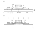
また、本発明の一態様は、透光性を有する第1の導電層で設けられた第1の電極と、第1
の電極に電気的に接続され、第1の導電層と第1の導電層より抵抗が低い第2の導電層と
の積層構造で設けられた第1の配線と、第1の電極及び第1の配線上に設けられた絶縁層
と、絶縁層上に設けられ、透光性を有する第3の導電層で設けられた第2の電極と、第2
の電極に電気的に接続され、第3の導電層と第3の導電層より抵抗が低い第4の導電層と
の積層構造で設けられた第2の配線と、透光性を有する第5の導電層で設けられた第3の
電極と、絶縁層上に第1の電極と重なるように設けられると共に、第2の電極及び第3の
電極上に設けられた半導体層を有する半導体装置を提供する。
One embodiment of the present invention includes a first electrode provided with a first light-transmitting conductive layer,
A first wiring provided in a stacked structure of a first conductive layer and a second conductive layer having a resistance lower than that of the first conductive layer, the first electrode, and the first electrode An insulating layer provided on the wiring, a second electrode provided on the insulating layer and provided with a light-transmitting third conductive layer, and a second electrode
A second wiring provided in a stacked structure of a third conductive layer and a fourth conductive layer having a resistance lower than that of the third conductive layer, electrically connected to the first electrode, and a light-transmitting fifth wire A semiconductor device having a third electrode provided by a conductive layer and a semiconductor layer provided on the insulating layer so as to overlap with the first electrode and provided on the second electrode and the third electrode. provide.
また、本発明の一態様は、透光性を有する第1の導電層で設けられた第1の電極と、第1
の電極と電気的に接続され、第1の導電層と第1の導電層より抵抗が低い第2の導電層と
の積層構造で設けられた第1の配線と、透光性を有する第3の導電層で設けられた第2の
配線と、第1の電極、第1の配線及び第2の配線上に設けられた絶縁層と、絶縁層上に設
けられ、透光性を有する第4の導電層で設けられた第2の電極と、第2の電極と電気的に
接続され、第4の導電層と第4の導電層より抵抗が低い第5の導電層との積層構造で設け
られた第3の配線と、透光性を有する第6の導電層で設けられた第3の電極と、第2の配
線上に絶縁層を介して設けられ、透光性を有する第7の導電層と、絶縁層上に第1の電極
と重なるように設けられると共に、第2の電極及び第3の電極上に設けられた半導体層を
有する半導体装置を提供する。
One embodiment of the present invention includes a first electrode provided with a first light-transmitting conductive layer,
A first wiring provided in a stacked structure of a first conductive layer and a second conductive layer having a resistance lower than that of the first conductive layer, and a third electrode having a light-transmitting property. A second wiring provided by the conductive layer, an insulating layer provided on the first electrode, the first wiring, and the second wiring, and a fourth light-transmitting material provided on the insulating layer. A second electrode provided in a conductive layer, and a stacked structure of a fourth conductive layer electrically connected to the second electrode and having a lower resistance than the fourth conductive layer and the fourth conductive layer. A third electrode provided by a sixth conductive layer having a light-transmitting property, a seventh electrode having a light-transmitting property, provided on the second wiring with an insulating layer interposed therebetween. Provided is a semiconductor device including a conductive layer and a semiconductor layer provided on the insulating layer so as to overlap with the first electrode and provided on the second electrode and the third electrode.
なお、スイッチは、様々な形態のものを用いることができる。例としては、電気的スイッ
チや機械的なスイッチなどがある。つまり、電流の流れを制御できるものであればよく、
特定のものに限定されない。例えば、スイッチとして、トランジスタ(例えば、バイポー
ラトランジスタ、MOSトランジスタなど)、ダイオード(例えば、PNダイオード、P
INダイオード、ショットキーダイオード、MIM(Metal Insulator
Metal)ダイオード、MIS(Metal Insulator Semicond
uctor)ダイオード、ダイオード接続のトランジスタなど)などを用いることが出来
る。または、これらを組み合わせた論理回路をスイッチとして用いることが出来る。
Note that various types of switches can be used. Examples include electrical switches and mechanical switches. In other words, anything that can control the current flow,
It is not limited to a specific thing. For example, as a switch, a transistor (for example, bipolar transistor, MOS transistor, etc.), a diode (for example, PN diode, P, etc.)
IN diode, Schottky diode, MIM (Metal Insulator)
Metal diode, MIS (Metal Insulator Semiconductor)
(e.g., a diode, a diode-connected transistor, or the like). Alternatively, a logic circuit combining these can be used as a switch.
機械的なスイッチの例としては、デジタルマイクロミラーデバイス(DMD)のように、
MEMS(マイクロ・エレクトロ・メカニカル・システム)技術を用いたスイッチがある
。そのスイッチは、機械的に動かすことが出来る電極を有し、その電極が動くことによっ
て、導通と非導通とを制御して動作する。
An example of a mechanical switch is a digital micromirror device (DMD),
There is a switch using MEMS (micro electro mechanical system) technology. The switch has an electrode that can be moved mechanically, and operates by controlling conduction and non-conduction by moving the electrode.
スイッチとしてトランジスタを用いる場合、そのトランジスタは、単なるスイッチとして
動作するため、トランジスタの極性(導電型)は特に限定されない。ただし、オフ電流を
抑えたい場合、オフ電流が少ない方の極性のトランジスタを用いることが望ましい。オフ
電流が少ないトランジスタとしては、LDD領域を有するトランジスタやマルチゲート構
造を有するトランジスタ等がある。または、スイッチとして動作させるトランジスタのソ
ース端子の電位が、低電位側電源(Vss、GND、0Vなど)の電位に近い値で動作す
る場合はNチャネル型トランジスタを用いることが望ましい。反対に、ソース端子の電位
が、高電位側電源(Vddなど)の電位に近い値で動作する場合はPチャネル型トランジ
スタを用いることが望ましい。なぜなら、Nチャネル型トランジスタではソース端子が低
電位側電源の電位に近い値で動作するとき、Pチャネル型トランジスタではソース端子が
高電位側電源の電位に近い値で動作するとき、ゲートとソースの間の電圧の絶対値を大き
くできるため、スイッチとして、より正確な動作を行うことができるからである。さらに
、トランジスタがソースフォロワ動作をしてしまうことが少ないため、出力電圧の大きさ
が小さくなってしまうことが少ないからである。
In the case where a transistor is used as a switch, the transistor operates as a mere switch, and thus the polarity (conductivity type) of the transistor is not particularly limited. However, when it is desired to suppress off-state current, it is desirable to use a transistor having a polarity with smaller off-state current. As a transistor with low off-state current, a transistor having an LDD region, a transistor having a multi-gate structure, and the like can be given. Alternatively, an N-channel transistor is preferably used when the potential of the source terminal of a transistor that operates as a switch operates at a value close to the potential of a low-potential power supply (Vss, GND, 0 V, or the like). On the other hand, when the potential of the source terminal operates at a value close to the potential of the high potential side power supply (Vdd or the like), it is desirable to use a P-channel transistor. This is because when the N-channel transistor operates at a value close to the potential of the low-potential side power supply, the P-channel transistor operates when the source terminal operates at a value close to the potential of the high-potential side power supply. This is because the absolute value of the voltage between them can be increased, so that more accurate operation can be performed as a switch. Further, since the transistor rarely performs a source follower operation, the magnitude of the output voltage is rarely reduced.
なお、Nチャネル型トランジスタとPチャネル型トランジスタの両方を用いて、CMOS
型のスイッチをスイッチとして用いてもよい。CMOS型のスイッチにすると、Pチャネ
ル型トランジスタまたはNチャネル型トランジスタのどちらか一方のトランジスタが導通
すれば電流が流れるため、スイッチとして機能しやすくなる。例えば、スイッチへの入力
信号の電圧が高い場合でも、低い場合でも、適切に電圧を出力させることが出来る。さら
に、スイッチをオンまたはオフさせるための信号の電圧振幅値を小さくすることが出来る
ので、消費電力を小さくすることも出来る。
Note that both N-channel and P-channel transistors are used for CMOS.
A type of switch may be used as the switch. When a CMOS switch is used, a current flows when one of the P-channel transistor and the N-channel transistor is turned on, so that the switch can easily function as a switch. For example, the voltage can be appropriately output regardless of whether the voltage of the input signal to the switch is high or low. Further, since the voltage amplitude value of the signal for turning on or off the switch can be reduced, power consumption can be reduced.
なお、スイッチとしてトランジスタを用いる場合、スイッチは、入力端子(ソース端子ま
たはドレイン端子の一方)と、出力端子(ソース端子またはドレイン端子の他方)と、導
通を制御する端子(ゲート端子)とを有している。一方、スイッチとしてダイオードを用
いる場合、スイッチは、導通を制御する端子を有していない場合がある。そのため、トラ
ンジスタよりもダイオードをスイッチとして用いた方が、端子を制御するための配線を少
なくすることが出来る。
Note that when a transistor is used as a switch, the switch has an input terminal (one of a source terminal or a drain terminal), an output terminal (the other of the source terminal or the drain terminal), and a terminal for controlling conduction (a gate terminal). doing. On the other hand, when a diode is used as the switch, the switch may not have a terminal for controlling conduction. Therefore, the use of a diode as a switch rather than a transistor can reduce the wiring for controlling the terminal.
なお、AとBとが接続されている、と明示的に記載する場合は、AとBとが電気的に接続
されている場合と、AとBとが機能的に接続されている場合と、AとBとが直接接続され
ている場合とを含むものとする。ここで、A、Bは、対象物(例えば、装置、素子、回路
、配線、電極、端子、導電膜、層、など)であるとする。したがって、所定の接続関係、
例えば、図または文章に示された接続関係に限定されず、図または文章に示された接続関
係以外のものも含むものとする。
In addition, when it is explicitly described that A and B are connected, A and B are electrically connected, and A and B are functionally connected. , A and B are directly connected. Here, A and B are objects (for example, devices, elements, circuits, wirings, electrodes, terminals, conductive films, layers, etc.). Therefore, the predetermined connection relationship,
For example, it is not limited to the connection relationship shown in the figure or text, and includes things other than the connection relationship shown in the figure or text.
例えば、AとBとが電気的に接続されている場合として、AとBとの電気的な接続を可能
とする素子(例えば、スイッチ、トランジスタ、容量素子、インダクタ、抵抗素子、ダイ
オードなど)が、AとBとの間に1個以上接続されていてもよい。あるいは、AとBとが
機能的に接続されている場合として、AとBとの機能的な接続を可能とする回路(例えば
、論理回路(インバータ、NAND回路、NOR回路など)、信号変換回路(DA変換回
路、AD変換回路、ガンマ補正回路など)、電位レベル変換回路(電源回路(昇圧回路、
降圧回路など)、信号の電位レベルを変えるレベルシフタ回路など)、電圧源、電流源、
切り替え回路、増幅回路(信号振幅または電流量などを大きく出来る回路、オペアンプ、
差動増幅回路、ソースフォロワ回路、バッファ回路など)、信号生成回路、記憶回路、制
御回路など)が、AとBとの間に1個以上接続されていてもよい。例えば、AとBとの間
に別の回路を挟んでいても、Aから出力された信号がBへ伝達される場合は、AとBとは
機能的に接続されているものとする。
For example, when A and B are electrically connected, an element (for example, a switch, a transistor, a capacitor, an inductor, a resistance element, a diode, or the like) that enables electrical connection between A and B is provided. , A and B may be connected one or more. Alternatively, when A and B are functionally connected, a circuit (for example, a logic circuit (an inverter, a NAND circuit, a NOR circuit, etc.), a signal conversion circuit that enables functional connection between A and B (DA conversion circuit, AD conversion circuit, gamma correction circuit, etc.), potential level conversion circuit (power supply circuit (boost circuit,
Step-down circuit), level shifter circuit that changes signal potential level), voltage source, current source,
Switching circuit, amplifier circuit (circuit that can increase signal amplitude or current, etc., operational amplifier,
One or more differential amplifier circuits, source follower circuits, buffer circuits, etc.), signal generation circuits, memory circuits, control circuits, etc.) may be connected between A and B. For example, even if another circuit is sandwiched between A and B, if the signal output from A is transmitted to B, it is assumed that A and B are functionally connected.
なお、AとBとが電気的に接続されている、と明示的に記載する場合は、AとBとが電気
的に接続されている場合(つまり、AとBとの間に別の素子や別の回路を挟んで接続され
ている場合)と、AとBとが機能的に接続されている場合(つまり、AとBとの間に別の
回路を挟んで機能的に接続されている場合)と、AとBとが直接接続されている場合(つ
まり、AとBとの間に別の素子や別の回路を挟まずに接続されている場合)とを含むもの
とする。つまり、電気的に接続されている、と明示的に記載する場合は、単に、接続され
ている、とのみ明示的に記載されている場合と同じであるとする。
Note that in the case where it is explicitly described that A and B are electrically connected, another element is connected between A and B (that is, between A and B). Or when A and B are functionally connected (that is, they are functionally connected with another circuit between A and B). And a case where A and B are directly connected (that is, a case where another element or another circuit is not connected between A and B). That is, when it is explicitly described that it is electrically connected, it is the same as when it is explicitly only described that it is connected.
なお、表示素子、表示素子を有する装置である表示装置、発光素子、発光素子を有する装
置である発光装置は、様々な形態を用いたり、様々な素子を有することが出来る。例えば
、表示素子、表示装置、発光素子または発光装置としては、EL(エレクトロルミネッセ
ンス)素子(有機物及び無機物を含むEL素子、有機EL素子、無機EL素子)、LED
(白色LED、赤色LED、緑色LED、青色LEDなど)、トランジスタ(電流に応じ
て発光するトランジスタ)、電子放出素子、液晶素子、電子インク、電気泳動素子、グレ
ーティングライトバルブ(GLV)、プラズマディスプレイ(PDP)、デジタルマイク
ロミラーデバイス(DMD)、圧電セラミックディスプレイ、カーボンナノチューブ、な
ど、電気磁気的作用により、コントラスト、輝度、反射率、透過率などが変化する表示媒
体を有することができる。なお、EL素子を用いた表示装置としてはELディスプレイ、
電子放出素子を用いた表示装置としてはフィールドエミッションディスプレイ(FED)
やSED方式平面型ディスプレイ(SED:Surface−conduction E
lectron−emitter Disply)など、液晶素子を用いた表示装置とし
ては液晶ディスプレイ(透過型液晶ディスプレイ、半透過型液晶ディスプレイ、反射型液
晶ディスプレイ、直視型液晶ディスプレイ、投射型液晶ディスプレイ)、電子インクや電
気泳動素子を用いた表示装置としては電子ペーパーがある。
Note that a display element, a display device that is a device including a display element, a light-emitting element, and a light-emitting device that is a device including a light-emitting element can have various modes or have various elements. For example, as a display element, a display device, a light-emitting element, or a light-emitting device, an EL (electroluminescence) element (an EL element including an organic substance and an inorganic substance, an organic EL element, an inorganic EL element), an LED
(White LED, red LED, green LED, blue LED, etc.), transistor (transistor that emits light in response to current), electron-emitting device, liquid crystal device, electronic ink, electrophoretic device, grating light valve (GLV), plasma display ( A display medium such as a PDP), a digital micromirror device (DMD), a piezoelectric ceramic display, a carbon nanotube, or the like that changes contrast, luminance, reflectance, transmittance, and the like by an electromagnetic action can be included. As a display device using an EL element, an EL display,
Field emission display (FED) is a display device using electron-emitting devices.
And SED type flat display (SED: Surface-conduction E)
As a display device using a liquid crystal element such as a electron-emitter display, a liquid crystal display (a transmissive liquid crystal display, a transflective liquid crystal display, a reflective liquid crystal display, a direct view liquid crystal display, a projection liquid crystal display), an electronic ink or an electric There is electronic paper as a display device using an electrophoretic element.
なお、EL素子とは、陽極と、陰極と、陽極と陰極との間に挟まれたEL層とを有する素
子である。なお、EL層としては、1重項励起子からの発光(蛍光)を利用するもの、3
重項励起子からの発光(燐光)を利用するもの、1重項励起子からの発光(蛍光)を利用
するものと3重項励起子からの発光(燐光)を利用するものとを含むもの、有機物によっ
て形成されたもの、無機物によって形成されたもの、有機物によって形成されたものと無
機物によって形成されたものとを含むもの、高分子の材料、低分子の材料、高分子の材料
と低分子の材料とを含むものなどを有することができる。ただし、これに限定されず、E
L素子として様々なものを有することができる。
Note that an EL element is an element having an anode, a cathode, and an EL layer sandwiched between the anode and the cathode. The EL layer uses light emission (fluorescence) from singlet excitons, 3
Those using light emission (phosphorescence) from singlet excitons, those using light emission (fluorescence) from singlet excitons, and those using light emission (phosphorescence) from triplet excitons , Organic materials, inorganic materials, organic materials and inorganic materials, high molecular materials, low molecular materials, high molecular materials and low molecules And the like. However, it is not limited to this, E
Various elements can be used as the L element.
なお、電子放出素子とは、陰極に高電界を集中して電子を引き出す素子である。例えば、
電子放出素子として、スピント型、カーボンナノチューブ(CNT)型、金属―絶縁体―
金属を積層したMIM(Metal−Insulator−Metal)型、金属―絶縁
体―半導体を積層したMIS(Metal−Insulator−Semiconduc
tor)型、MOS型、シリコン型、薄膜ダイオード型、ダイヤモンド型、表面伝導エミ
ッタSCD型、金属―絶縁体―半導体−金属型等の薄膜型、HEED型、EL型、ポーラ
スシリコン型、表面伝導(SCE)型などを有することができる。ただし、これに限定さ
れず、電子放出素子として様々なものを有することができる。
The electron-emitting device is a device that draws electrons by concentrating a high electric field on the cathode. For example,
As electron-emitting devices, Spindt type, carbon nanotube (CNT) type, metal-insulator-
MIM (Metal-Insulator-Metal) type laminated with metal, MIS (Metal-Insulator-Semiconductor) laminated with metal-insulator-semiconductor
tor) type, MOS type, silicon type, thin film diode type, diamond type, surface conduction emitter SCD type, metal-insulator-semiconductor-metal type thin film type, HEED type, EL type, porous silicon type, surface conduction ( SCE) type and the like. However, the present invention is not limited to this, and various electron-emitting devices can be used.
なお、液晶素子とは、液晶の光学的変調作用によって光の透過または非透過を制御する素
子であり、一対の電極、及び液晶により構成される。なお、液晶の光学的変調作用は、液
晶にかかる電界(横方向の電界、縦方向の電界又は斜め方向の電界を含む)によって制御
される。なお、液晶素子としては、ネマチック液晶、コレステリック液晶、スメクチック
液晶、ディスコチック液晶、サーモトロピック液晶、リオトロピック液晶、低分子液晶、
高分子液晶、高分子分散型液晶(PDLC)、強誘電液晶、反強誘電液晶、主鎖型液晶、
側鎖型高分子液晶、プラズマアドレス液晶(PALC)、バナナ型液晶、TN(Twis
ted Nematic)モード、STN(Super Twisted Nemati
c)モード、IPS(In−Plane−Switching)モード、FFS(Fri
nge Field Switching)モード、MVA(Multi−domain
Vertical Alignment)モード、PVA(Patterned Ve
rtical Alignment)、ASV(Advanced Super Vie
w)モード、ASM(Axially Symmetric aligned Micr
o−cell)モード、OCB(Optical Compensated Biref
ringence)モード、ECB(Electrically Controlled
Birefringence)モード、FLC(Ferroelectric Liq
uid Crystal)モード、AFLC(AntiFerroelectric L
iquid Crystal)モード、PDLC(Polymer Dispersed
Liquid Crystal)モード、ゲストホストモード、ブルー相(Blue
Phase)モードなどを用いることができる。ただし、これに限定されず、液晶素子と
して様々なものを用いることができる。
Note that a liquid crystal element is an element that controls transmission or non-transmission of light by an optical modulation action of liquid crystal, and includes a pair of electrodes and liquid crystal. Note that the optical modulation action of the liquid crystal is controlled by an electric field applied to the liquid crystal (including a horizontal electric field, a vertical electric field, or an oblique electric field). As liquid crystal elements, nematic liquid crystal, cholesteric liquid crystal, smectic liquid crystal, discotic liquid crystal, thermotropic liquid crystal, lyotropic liquid crystal, low molecular liquid crystal,
Polymer liquid crystal, polymer dispersed liquid crystal (PDLC), ferroelectric liquid crystal, antiferroelectric liquid crystal, main chain liquid crystal,
Side chain type polymer liquid crystal, plasma addressed liquid crystal (PALC), banana type liquid crystal, TN (Twis)
ted Nematic) mode, STN (Super Twisted Nematic)
c) mode, IPS (In-Plane-Switching) mode, FFS (Fri)
nge Field Switching mode, MVA (Multi-domain)
Vertical Alignment mode, PVA (Patterned Ve)
Vertical Alignment), ASV (Advanced Super Vie)
w) mode, ASM (Axial Symmetrical Aligned Micro)
o-cell) mode, OCB (Optical Compensated Biref)
ringence) mode, ECB (Electrically Controlled)
Birefringence mode, FLC (Ferroelectric Liq)
uid Crystal) mode, AFLC (Antiferroelectric L)
liquid crystal) mode, PDLC (Polymer Dispersed)
Liquid Crystal mode, guest host mode, blue phase (Blue)
Phase) mode or the like can be used. However, the present invention is not limited to this, and various liquid crystal elements can be used.
なお、電子ペーパーとしては、分子により表示されるもの(光学異方性、染料分子配向な
ど)、粒子により表示されるもの(電気泳動、粒子移動、粒子回転、相変化など)、フィ
ルムの一端が移動することにより表示されるもの、分子の発色/相変化により表示される
もの、分子の光吸収により表示されるもの、電子とホールが結合して自発光により表示さ
れるものなどのことをいう。例えば、電子ペーパーとして、マイクロカプセル型電気泳動
、水平移動型電気泳動、垂直移動型電気泳動、球状ツイストボール、磁気ツイストボール
、円柱ツイストボール方式、帯電トナー、電子粉流体(株式会社ブリヂストンの登録商標
)、磁気泳動型、磁気感熱式、エレクトロウェッテイング、光散乱(透明白濁)、コレス
テリック液晶/光導電層、コレステリック液晶、双安定性ネマチック液晶、強誘電性液晶
、2色性色素・液晶分散型、可動フィルム、ロイコ染料発消色、フォトクロミック、エレ
クトロクロミック、エレクトロデポジション、フレキシブル有機ELなどを用いることが
できる。ただし、これに限定されず、電子ペーパーとして様々なものを用いることができ
る。ここで、マイクロカプセル型電気泳動を用いることによって、電気泳動方式の欠点で
ある泳動粒子の凝集、沈殿を解決することができる。電子粉流体は、高速応答性、高反射
率、広視野角、低消費電力、メモリ性などのメリットを有する。
Electronic paper includes those displayed by molecules (optical anisotropy, dye molecule orientation, etc.), those displayed by particles (electrophoresis, particle movement, particle rotation, phase change, etc.), and one end of the film. It is displayed by moving, displayed by color development / phase change of molecules, displayed by light absorption of molecules, displayed by self-emission by combining electrons and holes, etc. . For example, as electronic paper, microcapsule type electrophoresis, horizontal movement type electrophoresis, vertical movement type electrophoresis, spherical twist ball, magnetic twist ball, cylindrical twist ball method, charged toner, electronic powder fluid (registered trademark of Bridgestone Corporation) ), Magnetophoretic, magnetic thermosensitive, electrowetting, light scattering (transparent white turbidity), cholesteric liquid crystal / photoconductive layer, cholesteric liquid crystal, bistable nematic liquid crystal, ferroelectric liquid crystal, dichroic dye / liquid crystal dispersion type , Movable film, leuco dye color-decoloring, photochromic, electrochromic, electrodeposition, flexible organic EL, and the like can be used. However, the present invention is not limited to this, and various electronic papers can be used. Here, by using microcapsule electrophoresis, aggregation and precipitation of electrophoretic particles, which is a drawback of the electrophoresis system, can be solved. The electronic powder fluid has advantages such as high-speed response, high reflectivity, wide viewing angle, low power consumption, and memory properties.
なお、プラズマディスプレイは、電極を表面に形成した基板と、電極及び微小な溝を表面
に形成し且つ溝内に蛍光体層を形成した基板とを狭い間隔で対向させて、希ガスを封入し
た構造を有する。あるいは、プラズマディスプレイは、プラズマチューブを上下からフィ
ルム状の電極で挟み込んだ構造とすることも可能である。プラズマチューブとは、ガラス
チューブ内に、放電ガス、RGBそれぞれの蛍光体などを封止したものである。なお、電
極間に電圧をかけることによって紫外線を発生させ、蛍光体を光らせることで、表示を行
うことができる。なお、プラズマディスプレイとしては、DC型PDP、AC型PDPで
もよい。ここで、プラズマディスプレイパネルとしては、ASW(Address Wh
ile Sustain)駆動、サブフレームをリセット期間、アドレス期間、維持期間
に分割するADS(Address Display Separated)駆動、CL
EAR(HIGH‐CONTRAST&LOW ENERGY ADDRESS&RED
UCTION OF FALSE CONTOUR SEQUENCE)駆動、ALIS
(Alternate Lighting of Surfaces)方式、TERES
(Techbology of Reciprocal Susfainer)駆動など
を用いることができる。ただし、これに限定されず、プラズマディスプレイとして様々な
ものを用いることができる。
Note that the plasma display encloses a rare gas with a substrate having an electrode formed on the surface and a substrate having an electrode and a minute groove formed on the surface and a phosphor layer formed in the groove facing each other at a narrow interval. It has a structure. Alternatively, the plasma display may have a structure in which a plasma tube is sandwiched between upper and lower film-like electrodes. The plasma tube is formed by sealing a discharge gas, RGB phosphors, and the like in a glass tube. In addition, a display can be performed by generating an ultraviolet-ray by applying a voltage between electrodes and making fluorescent substance light. The plasma display may be a DC type PDP or an AC type PDP. Here, as a plasma display panel, ASW (Address Wh
ile Sustain) drive, ADS (Address Display Separated) drive that divides a subframe into a reset period, an address period, and a sustain period, CL
EAR (HIGH-CONTRAST & LOW ENERGY ADDRESS & RED
UCTION OF FALSE CONTOUR SEQUENCE) drive, ALIS
(Alternate Lightning of Surfaces) method, TERES
(Technology of Reciprocal Susfainer) driving or the like can be used. However, the present invention is not limited to this, and various types of plasma displays can be used.
なお、光源を必要とする表示装置、例えば、液晶ディスプレイ(透過型液晶ディスプレイ
、半透過型液晶ディスプレイ、反射型液晶ディスプレイ、直視型液晶ディスプレイ、投射
型液晶ディスプレイ)、グレーティングライトバルブ(GLV)を用いた表示装置、デジ
タルマイクロミラーデバイス(DMD)を用いた表示装置などの光源としては、エレクト
ロルミネッセンス、冷陰極管、熱陰極管、LED、レーザー光源、水銀ランプなどを用い
ることができる。ただし、これに限定されず、光源して様々なものを用いることができる
。
Note that a display device that requires a light source, such as a liquid crystal display (transmission type liquid crystal display, transflective type liquid crystal display, reflection type liquid crystal display, direct view type liquid crystal display, projection type liquid crystal display), or a grating light valve (GLV) is used. As a light source for a display device using a conventional display device or a digital micromirror device (DMD), electroluminescence, a cold cathode tube, a hot cathode tube, an LED, a laser light source, a mercury lamp, or the like can be used. However, the present invention is not limited to this, and various light sources can be used.
なお、トランジスタとして、様々な形態のトランジスタを用いることが出来る。よって、
用いるトランジスタの種類に限定はない。例えば、非晶質シリコン、多結晶シリコン、微
結晶(マイクロクリスタル、ナノクリスタル、セミアモルファスとも言う)シリコンなど
に代表される非単結晶半導体膜を有する薄膜トランジスタ(TFT)などを用いることが
出来る。TFTを用いる場合、様々なメリットがある。例えば、単結晶シリコンの場合よ
りも低い温度で製造できるため、製造コストの削減、又は製造装置の大型化を図ることが
できる。製造装置を大きくできるため、大型基板上に製造できる。そのため、同時に多く
の個数の表示装置を製造できるため、低コストで製造できる。さらに、製造温度が低いた
め、耐熱性の弱い基板を用いることができる。そのため、透光性を有する基板上にトラン
ジスタを製造できる。そして、透光性を有する基板上のトランジスタを用いて表示素子で
の光の透過を制御することが出来る。あるいは、トランジスタの膜厚が薄いため、トラン
ジスタを構成する膜の一部は、光を透過させることが出来る。そのため、開口率が向上さ
せることができる。
Note that various types of transistors can be used as the transistor. Therefore,
There is no limitation on the type of transistor used. For example, a thin film transistor (TFT) including a non-single-crystal semiconductor film typified by amorphous silicon, polycrystalline silicon, microcrystalline (also referred to as microcrystal, nanocrystal, or semi-amorphous) silicon can be used. When using TFT, there are various advantages. For example, since manufacturing can be performed at a lower temperature than that of single crystal silicon, manufacturing cost can be reduced or a manufacturing apparatus can be increased in size. Since the manufacturing apparatus can be enlarged, it can be manufactured on a large substrate. Therefore, since a large number of display devices can be manufactured at the same time, it can be manufactured at low cost. Furthermore, since the manufacturing temperature is low, a substrate with low heat resistance can be used. Therefore, a transistor can be manufactured over a light-transmitting substrate. Then, transmission of light through the display element can be controlled using a transistor over a light-transmitting substrate. Alternatively, since the thickness of the transistor is small, part of the film included in the transistor can transmit light. Therefore, the aperture ratio can be improved.
なお、多結晶シリコンを製造するときに、触媒(ニッケルなど)を用いることにより、結
晶性をさらに向上させ、電気特性のよいトランジスタを製造することが可能となる。その
結果、ゲートドライバ回路(走査線駆動回路)やソースドライバ回路(信号線駆動回路)
、信号処理回路(信号生成回路、ガンマ補正回路、DA変換回路など)を基板上に一体形
成することが出来る。
Note that by using a catalyst (such as nickel) when manufacturing polycrystalline silicon, it is possible to further improve crystallinity and to manufacture a transistor with favorable electrical characteristics. As a result, a gate driver circuit (scan line driver circuit) and a source driver circuit (signal line driver circuit)
The signal processing circuit (signal generation circuit, gamma correction circuit, DA conversion circuit, etc.) can be integrally formed on the substrate.
なお、微結晶シリコンを製造するときに、触媒(ニッケルなど)を用いることにより、結
晶性をさらに向上させ、電気特性のよいトランジスタを製造することが可能となる。この
とき、レーザー照射を行うことなく、熱処理を加えるだけで、結晶性を向上させることも
可能である。その結果、ソースドライバ回路の一部(アナログスイッチなど)およびゲー
トドライバ回路(走査線駆動回路)を基板上に一体形成することが出来る。さらに、結晶
化のためにレーザー照射を行わない場合は、シリコンの結晶性のムラを抑えることができ
る。そのため、画質の向上した画像を表示することが出来る。
Note that when a microcrystalline silicon is manufactured, by using a catalyst (such as nickel), crystallinity can be further improved and a transistor with favorable electrical characteristics can be manufactured. At this time, it is also possible to improve crystallinity only by performing heat treatment without performing laser irradiation. As a result, part of the source driver circuit (such as an analog switch) and a gate driver circuit (scanning line driver circuit) can be formed over the substrate. Furthermore, in the case where laser irradiation is not performed for crystallization, the crystallinity unevenness of silicon can be suppressed. Therefore, an image with improved image quality can be displayed.
ただし、触媒(ニッケルなど)を用いずに、多結晶シリコンや微結晶シリコンを製造する
ことは可能である。
However, it is possible to produce polycrystalline silicon or microcrystalline silicon without using a catalyst (such as nickel).
なお、シリコンの結晶性を、多結晶または微結晶などへと向上させることは、パネル全体
で行うことが望ましいが、それに限定されない。パネルの一部の領域のみにおいて、シリ
コンの結晶性を向上させてもよい。選択的に結晶性を向上させることは、レーザー光を選
択的に照射することなどにより可能である。例えば、画素以外の領域である周辺回路領域
にのみ、レーザー光を照射してもよい。または、ゲートドライバ回路、ソースドライバ回
路等の領域にのみ、レーザー光を照射してもよい。あるいは、ソースドライバ回路の一部
(例えば、アナログスイッチ)の領域にのみ、レーザー光を照射してもよい。その結果、
回路を高速に動作させる必要がある領域にのみ、シリコンの結晶化を向上させることがで
きる。画素領域は、高速に動作させる必要性が低いため、結晶性が向上されなくても、問
題なく画素回路を動作させることが出来る。結晶性を向上させる領域が少なくて済むため
、製造工程も短くすることが出来、スループットが向上し、製造コストを低減させること
が出来る。必要とされる製造装置の数も少ない数で製造できるため、製造コストを低減さ
せることが出来る。
Note that it is preferable to improve the crystallinity of silicon to be polycrystalline or microcrystalline, but the present invention is not limited to this. The crystallinity of silicon may be improved only in a partial region of the panel. The crystallinity can be selectively improved by selectively irradiating laser light. For example, the laser beam may be irradiated only to the peripheral circuit region that is a region other than the pixel. Alternatively, the laser beam may be irradiated only on a region such as a gate driver circuit or a source driver circuit. Or you may irradiate a laser beam only to the area | region (for example, analog switch) of a source driver circuit. as a result,
Silicon crystallization can be improved only in regions where the circuit needs to operate at high speed. Since it is not necessary to operate the pixel region at high speed, the pixel circuit can be operated without any problem even if the crystallinity is not improved. Since a region for improving crystallinity is small, a manufacturing process can be shortened, throughput can be improved, and manufacturing cost can be reduced. Since the number of manufacturing apparatuses required can be reduced, the manufacturing cost can be reduced.
または、半導体基板やSOI基板などを用いてトランジスタを形成することが出来る。こ
れらにより、特性やサイズや形状などのバラツキが少なく、電流供給能力が高く、サイズ
の小さいトランジスタを製造することができる。これらのトランジスタを用いると、回路
の低消費電力化、又は回路の高集積化を図ることができる。
Alternatively, a transistor can be formed using a semiconductor substrate, an SOI substrate, or the like. Accordingly, a transistor with small variations in characteristics, size, shape, and the like, high current supply capability, and small size can be manufactured. When these transistors are used, low power consumption of the circuit or high integration of the circuit can be achieved.
または、ZnO、a−InGaZnO、SiGe、GaAs、IZO、ITO、SnO、
TiO、AlZnSnO(AZTO)などの化合物半導体または酸化物半導体を有するト
ランジスタや、さらに、これらの化合物半導体または酸化物半導体を薄膜化した薄膜トラ
ンジスタなどを用いることが出来る。これらにより、製造温度を低くでき、例えば、室温
でトランジスタを製造することが可能となる。その結果、耐熱性の低い基板、例えばプラ
スチック基板やフィルム基板に直接トランジスタを形成することが出来る。なお、これら
の化合物半導体または酸化物半導体を、トランジスタのチャネル部分に用いるだけでなく
、それ以外の用途で用いることも出来る。例えば、これらの化合物半導体または酸化物半
導体を抵抗素子、画素電極、透光性を有する電極として用いることができる。さらに、そ
れらをトランジスタと同時に成膜又は形成できるため、コストを低減できる。
Or ZnO, a-InGaZnO, SiGe, GaAs, IZO, ITO, SnO,
A transistor including a compound semiconductor or an oxide semiconductor such as TiO or AlZnSnO (AZTO), a thin film transistor obtained by thinning the compound semiconductor or the oxide semiconductor, or the like can be used. Accordingly, the manufacturing temperature can be lowered, and for example, the transistor can be manufactured at room temperature. As a result, the transistor can be formed directly on a substrate having low heat resistance, such as a plastic substrate or a film substrate. Note that these compound semiconductors or oxide semiconductors can be used not only for a channel portion of a transistor but also for other purposes. For example, these compound semiconductors or oxide semiconductors can be used as a resistance element, a pixel electrode, and a light-transmitting electrode. Furthermore, since these can be formed or formed simultaneously with the transistor, cost can be reduced.
または、インクジェットや印刷法を用いて形成したトランジスタなどを用いることが出来
る。これらにより、室温で製造、低真空度で製造、又は大型基板上に製造することができ
る。マスク(レチクル)を用いなくても製造することが可能となるため、トランジスタの
レイアウトを容易に変更することが出来る。さらに、レジストを用いる必要がないので、
材料費が安くなり、工程数を削減できる。さらに、必要な部分にのみ膜を付けるため、全
面に成膜した後でエッチングする、という製法よりも、材料が無駄にならず、低コストに
できる。
Alternatively, a transistor formed using an inkjet method or a printing method can be used. By these, it can manufacture at room temperature, manufacture at a low vacuum degree, or can manufacture on a large sized board | substrate. Since the transistor can be manufactured without using a mask (reticle), the layout of the transistor can be easily changed. Furthermore, since there is no need to use a resist,
Material costs are reduced and the number of processes can be reduced. Further, since a film is formed only on a necessary portion, the material is not wasted and cost can be reduced as compared with a manufacturing method in which etching is performed after film formation on the entire surface.
または、有機半導体やカーボンナノチューブを有するトランジスタ等を用いることができ
る。これらにより、曲げることが可能な基板上にトランジスタを形成することが出来る。
このような基板を用いた半導体装置は、衝撃に強くすることができる。
Alternatively, a transistor including an organic semiconductor or a carbon nanotube can be used. Thus, a transistor can be formed over a substrate that can be bent.
A semiconductor device using such a substrate can be resistant to impact.
さらに、様々な構造のトランジスタを用いることができる。例えば、MOS型トランジス
タ、接合型トランジスタ、バイポーラトランジスタなどをトランジスタとして用いること
が出来る。MOS型トランジスタを用いることにより、トランジスタのサイズを小さくす
ることが出来る。よって、複数のトランジスタを搭載することができる。バイポーラトラ
ンジスタを用いることにより、大きな電流を流すことが出来る。よって、高速に回路を動
作させることができる。
In addition, transistors with various structures can be used. For example, a MOS transistor, a junction transistor, a bipolar transistor, or the like can be used as the transistor. By using a MOS transistor, the size of the transistor can be reduced. Thus, a plurality of transistors can be mounted. By using a bipolar transistor, a large current can flow. Therefore, the circuit can be operated at high speed.
なお、MOS型トランジスタ、バイポーラトランジスタなどを1つの基板に混在させて形
成してもよい。これにより、低消費電力、小型化、高速動作などを実現することが出来る
。
Note that a MOS transistor, a bipolar transistor, or the like may be formed over one substrate. Thereby, low power consumption, miniaturization, high-speed operation, etc. can be realized.
その他、様々なトランジスタを用いることができる。 In addition, various transistors can be used.
なお、トランジスタは、様々な基板を用いて形成することが出来る。基板の種類は、特定
のものに限定されることはない。その基板としては、例えば、単結晶基板(例えばシリコ
ン基板)、SOI基板、ガラス基板、石英基板、プラスチック基板、金属基板、ステンレ
ス・スチル基板、ステンレス・スチル・ホイルを有する基板、タングステン基板、タング
ステン・ホイルを有する基板、可撓性基板などを用いることが出来る。ガラス基板の一例
としては、バリウムホウケイ酸ガラス、アルミノホウケイ酸ガラスなどがある。可撓性基
板の一例としては、ポリエチレンテレフタレート(PET)、ポリエチレンナフタレート
(PEN)、ポリエーテルサルフォン(PES)に代表されるプラスチック、又はアクリ
ル等の可撓性を有する合成樹脂などがある。他にも、貼り合わせフィルム(ポリプロピレ
ン、ポリエステル、ビニル、ポリフッ化ビニル、塩化ビニルなど)、繊維状な材料を含む
紙、基材フィルム(ポリエステル、ポリアミド、ポリイミド、無機蒸着フィルム、紙類等
)などがある。または、ある基板を用いてトランジスタを形成し、その後、別の基板にト
ランジスタを転置し、別の基板上にトランジスタを配置してもよい。トランジスタが転置
される基板としては、単結晶基板、SOI基板、ガラス基板、石英基板、プラスチック基
板、紙基板、セロファン基板、石材基板、木材基板、布基板(天然繊維(絹、綿、麻)、
合成繊維(ナイロン、ポリウレタン、ポリエステル)若しくは再生繊維(アセテート、キ
ュプラ、レーヨン、再生ポリエステル)などを含む)、皮革基板、ゴム基板、ステンレス
・スチル基板、ステンレス・スチル・ホイルを有する基板などを用いることができる。あ
るいは、人などの動物の皮膚(表皮、真皮)又は皮下組織を基板として用いてもよい。ま
たは、ある基板を用いてトランジスタを形成し、その基板を研磨して薄くしてもよい。研
磨される基板としては、単結晶基板、SOI基板、ガラス基板、石英基板、プラスチック
基板、ステンレス・スチル基板、ステンレス・スチル・ホイルを有する基板などを用いる
ことができる。これらの基板を用いることにより、特性のよいトランジスタの形成、消費
電力の小さいトランジスタの形成、壊れにくい装置の製造、耐熱性の付与、軽量化、又は
薄型化を図ることができる。
Note that the transistor can be formed using various substrates. The kind of board | substrate is not limited to a specific thing. As the substrate, for example, a single crystal substrate (for example, a silicon substrate), an SOI substrate, a glass substrate, a quartz substrate, a plastic substrate, a metal substrate, a stainless steel substrate, a substrate having stainless steel foil, a tungsten substrate, a tungsten substrate, A substrate having a foil, a flexible substrate, or the like can be used. Examples of the glass substrate include barium borosilicate glass and alumino borosilicate glass. As an example of the flexible substrate, there are plastics typified by polyethylene terephthalate (PET), polyethylene naphthalate (PEN), and polyethersulfone (PES), or a synthetic resin having flexibility such as acrylic. In addition, laminated films (polypropylene, polyester, vinyl, polyvinyl fluoride, vinyl chloride, etc.), paper containing fibrous materials, substrate films (polyester, polyamide, polyimide, inorganic vapor deposition film, papers, etc.), etc. There is. Alternatively, a transistor may be formed using a certain substrate, and then the transistor may be transferred to another substrate, and the transistor may be disposed on another substrate. As a substrate to which the transistor is transferred, a single crystal substrate, an SOI substrate, a glass substrate, a quartz substrate, a plastic substrate, a paper substrate, a cellophane substrate, a stone substrate, a wood substrate, a cloth substrate (natural fiber (silk, cotton, hemp),
Use synthetic fibers (nylon, polyurethane, polyester) or recycled fibers (including acetate, cupra, rayon, recycled polyester), leather substrates, rubber substrates, stainless steel substrates, substrates with stainless steel foil, etc. Can do. Alternatively, the skin (epidermis, dermis) or subcutaneous tissue of animals such as humans may be used as the substrate. Alternatively, a transistor may be formed using a certain substrate, and the substrate may be polished and thinned. As a substrate to be polished, a single crystal substrate, an SOI substrate, a glass substrate, a quartz substrate, a plastic substrate, a stainless steel substrate, a substrate having stainless steel foil, or the like can be used. By using these substrates, it is possible to form a transistor with good characteristics, a transistor with low power consumption, manufacture a device that is not easily broken, impart heat resistance, reduce weight, or reduce thickness.
なお、トランジスタの構成は、様々な形態をとることができ、特定の構成に限定されない
。例えば、ゲート電極が2個以上のマルチゲート構造を適用することができる。マルチゲ
ート構造にすると、チャネル領域が直列に接続されるため、複数のトランジスタが直列に
接続された構成となる。マルチゲート構造により、オフ電流の低減、トランジスタの耐圧
向上(信頼性の向上)を図ることができる。あるいは、マルチゲート構造により、飽和領
域で動作する時に、ドレイン・ソース間電圧が変化しても、ドレイン・ソース間電流があ
まり変化せず、電圧・電流特性の傾きをフラットにすることができる。電圧・電流特性の
傾きがフラットである特性を利用すると、理想的な電流源回路や、非常に高い抵抗値をも
つ能動負荷を実現することが出来る。その結果、特性のよい差動回路やカレントミラー回
路を実現することが出来る。
Note that the structure of the transistor can take a variety of forms and is not limited to a specific structure. For example, a multi-gate structure having two or more gate electrodes can be applied. When the multi-gate structure is employed, the channel regions are connected in series, so that a plurality of transistors are connected in series. With the multi-gate structure, off-state current can be reduced and the breakdown voltage of the transistor can be improved (reliability improvement). Alternatively, with the multi-gate structure, even when the drain-source voltage changes, the drain-source current does not change much when operating in the saturation region, and the slope of the voltage / current characteristics can be flattened. By using the characteristic that the slope of the voltage / current characteristic is flat, an ideal current source circuit and an active load having a very high resistance value can be realized. As a result, a differential circuit or a current mirror circuit with good characteristics can be realized.
別の例として、チャネルの上下にゲート電極が配置されている構造を適用することができ
る。チャネルの上下にゲート電極が配置されている構造にすることにより、チャネル領域
が増えるため、電流値の増加を図ることができる。または、チャネルの上下にゲート電極
が配置されている構造にすることにより、空乏層ができやすくなるため、S値の改善を図
ることができる。なお、チャネルの上下にゲート電極が配置される構成にすることにより
、複数のトランジスタが並列に接続されたような構成となる。
As another example, a structure in which gate electrodes are arranged above and below a channel can be applied. By employing a structure in which gate electrodes are arranged above and below the channel, the channel region increases, so that the current value can be increased. Alternatively, a structure in which gate electrodes are provided above and below a channel facilitates the formation of a depletion layer, so that the S value can be improved. Note that a structure in which a plurality of transistors are connected in parallel is obtained by using a structure in which gate electrodes are arranged above and below a channel.
チャネル領域の上にゲート電極が配置されている構造、チャネル領域の下にゲート電極が
配置されている構造、正スタガ構造、逆スタガ構造、チャネル領域を複数の領域に分けた
構造、チャネル領域を並列に接続した構造、またはチャネル領域が直列に接続する構成も
適用できる。さらに、チャネル領域(もしくはその一部)にソース電極やドレイン電極が
重なっている構造も適用できる。チャネル領域(もしくはその一部)にソース電極やドレ
イン電極が重なる構造にすることによって、チャネル領域の一部に電荷が溜まることによ
り動作が不安定になることを防ぐことができる。あるいは、LDD領域を設けた構造を適
用できる。LDD領域を設けることにより、オフ電流の低減、又はトランジスタの耐圧向
上(信頼性の向上)を図ることができる。あるいは、LDD領域を設けることにより、飽
和領域で動作する時に、ドレイン・ソース間電圧が変化しても、ドレイン・ソース間電流
があまり変化せず、電圧・電流特性の傾きがフラットな特性にすることができる。
A structure in which the gate electrode is arranged above the channel region, a structure in which the gate electrode is arranged under the channel region, a normal stagger structure, an inverted stagger structure, a structure in which the channel region is divided into a plurality of regions, and a channel region A structure connected in parallel or a configuration in which channel regions are connected in series can also be applied. Further, a structure in which a source electrode or a drain electrode overlaps with a channel region (or part of it) can be used. With the structure where the source electrode and the drain electrode overlap with the channel region (or part thereof), unstable operation due to accumulation of electric charge in part of the channel region can be prevented. Alternatively, a structure provided with an LDD region can be applied. By providing the LDD region, off-state current can be reduced or the breakdown voltage of the transistor can be improved (reliability improvement). Alternatively, by providing an LDD region, when operating in the saturation region, even if the drain-source voltage changes, the drain-source current does not change so much and the slope of the voltage-current characteristic is flat. be able to.
なお、トランジスタは、様々なタイプを用いることができ、様々な基板を用いて形成させ
ることができる。したがって、所定の機能を実現させるために必要な回路の全てが、同一
の基板に形成することも可能である。例えば、所定の機能を実現させるために必要な回路
の全てが、ガラス基板、プラスチック基板、単結晶基板、またはSOI基板などの様々な
基板を用いて形成することも可能である。所定の機能を実現させるために必要な回路の全
てが同じ基板を用いて形成されていることにより、部品点数の削減によるコストの低減、
又は回路部品との接続点数の低減による信頼性の向上を図ることができる。あるいは、所
定の機能を実現させるために必要な回路の一部が、ある基板に形成され、所定の機能を実
現させるために必要な回路の別の一部が、別の基板に形成されていることも可能である。
つまり、所定の機能を実現させるために必要な回路の全てが同じ基板を用いて形成されて
いなくてもよい。例えば、所定の機能を実現させるために必要な回路の一部は、ガラス基
板上にトランジスタにより形成され、所定の機能を実現させるために必要な回路の別の一
部は、単結晶基板に形成され、単結晶基板を用いて形成されたトランジスタで構成された
ICチップをCOG(Chip On Glass)でガラス基板に接続して、ガラス基
板上にそのICチップを配置することも可能である。あるいは、そのICチップをTAB
(Tape Automated Bonding)やプリント基板を用いてガラス基板
と接続することも可能である。このように、回路の一部が同じ基板に形成されていること
により、部品点数の削減によるコストの低減、又は回路部品との接続点数の低減による信
頼性の向上を図ることができる。あるいは、駆動電圧が高い部分及び駆動周波数が高い部
分の回路は、消費電力が大きくなってしまうので、そのような部分の回路は同じ基板に形
成せず、そのかわりに、例えば、単結晶基板にその部分の回路を形成して、その回路で構
成されたICチップを用いるようにすれば、消費電力の増加を防ぐことができる。
Note that various types of transistors can be used, and the transistor can be formed using various substrates. Therefore, all the circuits necessary for realizing a predetermined function can be formed on the same substrate. For example, all circuits necessary for realizing a predetermined function can be formed using various substrates such as a glass substrate, a plastic substrate, a single crystal substrate, or an SOI substrate. Since all the circuits necessary for realizing a predetermined function are formed using the same substrate, the cost can be reduced by reducing the number of parts.
Alternatively, reliability can be improved by reducing the number of connection points with circuit components. Alternatively, a part of the circuit necessary for realizing the predetermined function is formed on a certain substrate, and another part of the circuit necessary for realizing the predetermined function is formed on another substrate. It is also possible.
That is, not all the circuits necessary for realizing a predetermined function may be formed using the same substrate. For example, a part of a circuit necessary for realizing a predetermined function is formed by a transistor over a glass substrate, and another part of a circuit required for realizing a predetermined function is formed on a single crystal substrate. In addition, an IC chip including a transistor formed using a single crystal substrate can be connected to a glass substrate by COG (Chip On Glass), and the IC chip can be arranged on the glass substrate. Or the IC chip is TAB
It is also possible to connect to a glass substrate using (Tape Automated Bonding) or a printed circuit board. As described above, since a part of the circuit is formed on the same substrate, the cost can be reduced by reducing the number of components, or the reliability can be improved by reducing the number of connection points with circuit components. Alternatively, since the power consumption of a circuit with a high drive voltage and a high drive frequency is high, such a circuit is not formed on the same substrate. Instead, for example, a single crystal substrate is used. If a circuit for that portion is formed and an IC chip constituted by the circuit is used, an increase in power consumption can be prevented.
なお、一画素とは、明るさを制御できる要素一つ分を示すものとする。よって、一例とし
ては、一画素とは、一つの色要素を示すものとし、その色要素一つで明るさを表現する。
従って、そのときは、R(赤)G(緑)B(青)の色要素からなるカラー表示装置の場合
には、画像の最小単位は、Rの画素とGの画素とBの画素との三画素から構成されるもの
とする。なお、色要素は、三色に限定されず、三色以上を用いても良いし、RGB以外の
色を用いても良い。例えば、白色を加えて、RGBW(Wは白)としても可能である。あ
るいは、RGBに、例えば、イエロー、シアン、マゼンタ、エメラルドグリーン、朱色な
どを一色以上追加することも可能である。あるいは、例えば、RGBの中の少なくとも一
色に類似した色を、RGBに追加することも可能である。例えば、R、G、B1、B2と
してもよい。B1とB2とは、どちらも青色であるが、少し波長が異なっている。同様に
、R1、R2、G、Bとすることも可能である。このような色要素を用いることにより、
より実物に近い表示を行うことができる。このような色要素を用いることにより、消費電
力を低減することが出来る。別の例としては、一つの色要素について、複数の領域を用い
て明るさを制御する場合は、その領域一つ分を一画素とすることも可能である。よって、
一例として、面積階調を行う場合または副画素(サブ画素)を有している場合、一つの色
要素につき、明るさを制御する領域が複数あり、その全体で階調を表現するが、明るさを
制御する領域の一つ分を一画素とすることも可能である。よって、その場合は、一つの色
要素は、複数の画素で構成されることとなる。あるいは、明るさを制御する領域が一つの
色要素の中に複数あっても、それらをまとめて、一つの色要素を1画素としてもよい。よ
って、その場合は、一つの色要素は、一つの画素で構成されることとなる。あるいは、一
つの色要素について、複数の領域を用いて明るさを制御する場合、画素によって、表示に
寄与する領域の大きさが異なっている場合がある。あるいは、一つの色要素につき複数あ
る、明るさを制御する領域において、各々に供給する信号を僅かに異ならせるようにして
、視野角を広げるようにしてもよい。つまり、一つの色要素について、複数個ある領域が
各々有する画素電極の電位が、各々異なっていることも可能である。その結果、液晶分子
に加わる電圧が各画素電極によって各々異なる。よって、視野角を広くすることが出来る
。
One pixel means one element whose brightness can be controlled. Therefore, as an example, one pixel represents one color element, and brightness is expressed by one color element.
Therefore, at that time, in the case of a color display device composed of R (red), G (green), and B (blue) color elements, the minimum unit of an image is an R pixel, a G pixel, and a B pixel. It is assumed to be composed of three pixels. Note that the color elements are not limited to three colors, and three or more colors may be used, or colors other than RGB may be used. For example, RGBW (W is white) can be added by adding white. Alternatively, one or more colors such as yellow, cyan, magenta, emerald green, and vermilion can be added to RGB. Alternatively, for example, a color similar to at least one of RGB can be added to RGB. For example, R, G, B1, and B2 may be used. B1 and B2 are both blue, but have slightly different wavelengths. Similarly, R1, R2, G, and B can be used. By using such color elements,
A display closer to the real thing can be performed. By using such color elements, power consumption can be reduced. As another example, in the case where brightness is controlled using a plurality of areas for one color element, it is possible to use one area as one pixel. Therefore,
As an example, when area gradation is performed or when sub-pixels (sub-pixels) are provided, there are a plurality of areas for controlling the brightness for each color element, and the gradation is expressed as a whole. It is also possible to use one pixel as a region for controlling the height. Therefore, in that case, one color element is composed of a plurality of pixels. Alternatively, even if there are a plurality of areas for controlling the brightness in one color element, they may be combined into one pixel. Therefore, in that case, one color element is composed of one pixel. Alternatively, when the brightness is controlled using a plurality of areas for one color element, the size of the area contributing to display may be different depending on the pixel. Alternatively, the viewing angle may be widened by slightly varying the signal supplied to each of the areas where the brightness is controlled, which is plural for each color element. That is, the potentials of the pixel electrodes included in a plurality of regions for one color element may be different from each other. As a result, the voltage applied to the liquid crystal molecules is different for each pixel electrode. Therefore, the viewing angle can be widened.
なお、一画素(三色分)と明示的に記載する場合は、RとGとBの三画素分を一画素と考
える場合であるとする。一画素(一色分)と明示的に記載する場合は、一つの色要素につ
き、複数の領域がある場合、それらをまとめて一画素と考える場合であるとする。
In addition, when it is explicitly described as one pixel (for three colors), it is assumed that three pixels of R, G, and B are considered as one pixel. When it is explicitly described as one pixel (for one color), it is assumed that when there are a plurality of areas for one color element, they are considered as one pixel.
なお、画素は、マトリクス状に配置(配列)されている場合がある。ここで、画素がマト
リクスに配置(配列)されているとは、縦方向もしくは横方向において、画素が直線上に
並んで配置されている場合、又はギザギザな線上に配置されている場合を含む。よって、
例えば三色の色要素(例えばRGB)でフルカラー表示を行う場合に、ストライプ配置さ
れている場合、又は三つの色要素のドットがデルタ配置されている場合も含む。さらに、
ベイヤー配置されている場合も含む。なお、色要素のドット毎にその表示領域の大きさが
異なっていてもよい。これにより、低消費電力化、又は表示素子の長寿命化を図ることが
できる。
Note that the pixels may be arranged (arranged) in a matrix. Here, the arrangement (arrangement) of pixels in a matrix includes a case where pixels are arranged side by side in a vertical direction or a horizontal direction, or a case where they are arranged on a jagged line. Therefore,
For example, when full-color display is performed with three color elements (for example, RGB), the case where stripes are arranged or the case where dots of three color elements are arranged in a delta is included. further,
Including cases where Bayer is arranged. The size of the display area may be different for each dot of the color element. Thereby, it is possible to reduce power consumption or extend the life of the display element.
なお、画素に能動素子を有するアクティブマトリクス方式、または、画素に能動素子を有
しないパッシブマトリクス方式を用いることが出来る。
Note that an active matrix method in which an active element is included in a pixel or a passive matrix method in which an active element is not included in a pixel can be used.
アクティブマトリクス方式では、能動素子(アクティブ素子、非線形素子)として、トラ
ンジスタだけでなく、さまざまな能動素子(アクティブ素子、非線形素子)を用いること
が出来る。例えば、MIM(Metal Insulator Metal)やTFD(
Thin Film Diode)などを用いることも可能である。これらの素子は、製
造工程が少ないため、製造コストの低減、又は歩留まりの向上を図ることができる。さら
に、素子のサイズが小さいため、開口率を向上させることができ、低消費電力化や高輝度
化をはかることが出来る。
In the active matrix system, not only transistors but also various active elements (active elements and nonlinear elements) can be used as active elements (active elements and nonlinear elements). For example, MIM (Metal Insulator Metal) or TFD (
It is also possible to use (Thin Film Diode) or the like. Since these elements have few manufacturing steps, manufacturing cost can be reduced or yield can be improved. Furthermore, since the size of the element is small, the aperture ratio can be improved, and low power consumption and high luminance can be achieved.
なお、アクティブマトリクス方式以外のものとして、能動素子(アクティブ素子、非線形
素子)を用いないパッシブマトリクス型を用いることも可能である。能動素子(アクティ
ブ素子、非線形素子)を用いないため、製造工程が少なく、製造コストの低減、又は歩留
まりの向上を図ることができる。能動素子(アクティブ素子、非線形素子)を用いないた
め、開口率を向上させることができ、低消費電力化や高輝度化をはかることが出来る。
Note that as a method other than the active matrix method, a passive matrix type that does not use active elements (active elements, nonlinear elements) can be used. Since no active element (active element or nonlinear element) is used, the number of manufacturing steps is small, and manufacturing cost can be reduced or yield can be improved. Since no active element (active element or nonlinear element) is used, the aperture ratio can be improved, and low power consumption and high luminance can be achieved.
なお、トランジスタとは、ゲートと、ドレインと、ソースとを含む少なくとも三つの端子
を有する素子であり、ドレイン領域とソース領域の間にチャネル領域を有しており、ドレ
イン領域とチャネル領域とソース領域とを介して電流を流すことが出来る。ここで、ソー
スとドレインとは、トランジスタの構造や動作条件等によって変わるため、いずれがソー
スまたはドレインであるかを限定することが困難である。そこで、ソース及びドレインと
して機能する領域を、ソースもしくはドレインと呼ばない場合がある。その場合、一例と
しては、それぞれを第1端子、第2端子と表記する場合がある。あるいは、それぞれを第
1電極、第2電極と表記する場合がある。あるいは、第1領域、第2領域と表記する場合
がある。
Note that a transistor is an element having at least three terminals including a gate, a drain, and a source. The transistor has a channel region between the drain region and the source region, and the drain region, the channel region, and the source region. A current can be passed through. Here, since the source and the drain vary depending on the structure and operating conditions of the transistor, it is difficult to limit which is the source or the drain. Thus, a region functioning as a source and a drain may not be referred to as a source or a drain. In that case, as an example, there are cases where they are respectively referred to as a first terminal and a second terminal. Alternatively, they may be referred to as a first electrode and a second electrode, respectively. Alternatively, it may be referred to as a first area or a second area.
なお、トランジスタは、ベースとエミッタとコレクタとを含む少なくとも三つの端子を有
する素子であってもよい。この場合も同様に、エミッタとコレクタとを、第1端子、第2
端子などと表記する場合がある。
Note that the transistor may be an element having at least three terminals including a base, an emitter, and a collector. Similarly, in this case, the emitter and collector are connected to the first terminal and the second terminal.
Sometimes referred to as a terminal.
なお、ゲートとは、ゲート電極とゲート配線(ゲート線、ゲート信号線、走査線、走査信
号線等とも言う)とを含んだ全体、もしくは、それらの一部のことを言う。ゲート電極と
は、チャネル領域を形成する半導体と、ゲート絶縁膜を介してオーバーラップしている部
分の導電膜のことを言う。なお、ゲート電極の一部は、LDD(Lightly Dop
ed Drain)領域またはソース領域(またはドレイン領域)と、ゲート絶縁膜を介
してオーバーラップしている場合もある。ゲート配線とは、各トランジスタのゲート電極
の間を接続するための配線、各画素の有するゲート電極の間を接続するための配線、又は
ゲート電極と別の配線とを接続するための配線のことを言う。
Note that a gate refers to the whole or part of a gate electrode and a gate wiring (also referred to as a gate line, a gate signal line, a scan line, a scan signal line, or the like). A gate electrode refers to a portion of a conductive film that overlaps with a semiconductor forming a channel region with a gate insulating film interposed therebetween. Note that a part of the gate electrode is an LDD (Lightly Dop
ed Drain) region or source region (or drain region) may overlap with the gate insulating film. A gate wiring is a wiring for connecting the gate electrodes of each transistor, a wiring for connecting the gate electrodes of each pixel, or a wiring for connecting the gate electrode to another wiring. Say.
ただし、ゲート電極としても機能し、ゲート配線としても機能するような部分(領域、導
電膜、配線など)も存在する。そのような部分(領域、導電膜、配線など)は、ゲート電
極と呼んでも良いし、ゲート配線と呼んでも良い。つまり、ゲート電極とゲート配線とが
、明確に区別できないような領域も存在する。例えば、延伸して配置されているゲート配
線の一部とチャネル領域がオーバーラップしている場合、その部分(領域、導電膜、配線
など)はゲート配線として機能しているが、ゲート電極としても機能していることになる
。よって、そのような部分(領域、導電膜、配線など)は、ゲート電極と呼んでも良いし
、ゲート配線と呼んでも良い。
However, there are portions (regions, conductive films, wirings, etc.) that also function as gate electrodes and function as gate wirings. Such a portion (region, conductive film, wiring, or the like) may be called a gate electrode or a gate wiring. That is, there is a region where the gate electrode and the gate wiring cannot be clearly distinguished. For example, when a part of the gate wiring extended and the channel region overlap, the portion (region, conductive film, wiring, etc.) functions as the gate wiring, but also as the gate electrode It is functioning. Therefore, such a portion (region, conductive film, wiring, or the like) may be called a gate electrode or a gate wiring.
なお、ゲート電極と同じ材料で形成され、ゲート電極と同じ島(アイランド)を形成して
つながっている部分(領域、導電膜、配線など)も、ゲート電極と呼んでも良い。同様に
、ゲート配線と同じ材料で形成され、ゲート配線と同じ島(アイランド)を形成してつな
がっている部分(領域、導電膜、配線など)も、ゲート配線と呼んでも良い。このような
部分(領域、導電膜、配線など)は、厳密な意味では、チャネル領域とオーバーラップし
ていない場合、又は別のゲート電極と接続させる機能を有していない場合がある。しかし
、製造時の仕様などの関係で、ゲート電極またはゲート配線と同じ材料で形成され、ゲー
ト電極またはゲート配線と同じ島(アイランド)を形成してつながっている部分(領域、
導電膜、配線など)がある。よって、そのような部分(領域、導電膜、配線など)もゲー
ト電極またはゲート配線と呼んでも良い。
Note that a portion (a region, a conductive film, a wiring, or the like) formed using the same material as the gate electrode and connected to form the same island (island) as the gate electrode may be called a gate electrode. Similarly, a portion (a region, a conductive film, a wiring, or the like) formed using the same material as the gate wiring and connected by forming the same island (island) as the gate wiring may be referred to as a gate wiring. In a strict sense, such a portion (region, conductive film, wiring, or the like) may not overlap with the channel region or may not have a function of being connected to another gate electrode. However, due to the specifications at the time of manufacturing, etc., it is made of the same material as the gate electrode or gate wiring, and forms the same island (island) as the gate electrode or gate wiring (region,
Conductive film, wiring, etc.). Therefore, such a portion (region, conductive film, wiring, or the like) may also be referred to as a gate electrode or a gate wiring.
なお、例えば、マルチゲートのトランジスタにおいて、1つのゲート電極と、別のゲート
電極とは、ゲート電極と同じ材料で形成された導電膜で接続される場合が多い。そのよう
な部分(領域、導電膜、配線など)は、ゲート電極とゲート電極とを接続させるための部
分(領域、導電膜、配線など)であるため、ゲート配線と呼んでも良いが、マルチゲート
のトランジスタを1つのトランジスタと見なすことも出来るため、ゲート電極と呼んでも
良い。つまり、ゲート電極またはゲート配線と同じ材料で形成され、ゲート電極またはゲ
ート配線と同じ島(アイランド)を形成してつながっている部分(領域、導電膜、配線な
ど)は、ゲート電極やゲート配線と呼んでも良い。さらに、例えば、ゲート電極とゲート
配線とを接続させている部分の導電膜であって、ゲート電極またはゲート配線とは異なる
材料で形成された導電膜も、ゲート電極と呼んでも良いし、ゲート配線と呼んでも良い。
Note that, for example, in a multi-gate transistor, one gate electrode and another gate electrode are often connected to each other with a conductive film formed using the same material as the gate electrode. Such a portion (region, conductive film, wiring, or the like) is a portion (region, conductive film, wiring, or the like) for connecting the gate electrode to the gate electrode, and may be called a gate wiring. These transistors can be regarded as a single transistor, and may be referred to as a gate electrode. That is, a portion (region, conductive film, wiring, or the like) that is formed using the same material as the gate electrode or gate wiring and is connected to form the same island (island) as the gate electrode or gate wiring is connected to the gate electrode or gate wiring. You can call it. Further, for example, a conductive film in a portion where the gate electrode and the gate wiring are connected and formed of a material different from the gate electrode or the gate wiring may be referred to as a gate electrode. You may call it.
なお、ゲート端子とは、ゲート電極の部分(領域、導電膜、配線など)または、ゲート電
極と電気的に接続されている部分(領域、導電膜、配線など)について、その一部分のこ
とを言う。
Note that a gate terminal means a part of a part of a gate electrode (a region, a conductive film, a wiring, or the like) or a part electrically connected to the gate electrode (a region, a conductive film, a wiring, or the like). .
なお、ある配線を、ゲート配線、ゲート線、ゲート信号線、走査線、走査信号線などと呼
ぶ場合、その配線にトランジスタのゲートが接続されていない場合もある。この場合、ゲ
ート配線、ゲート線、ゲート信号線、走査線、走査信号線は、トランジスタのゲートと同
じ層で形成された配線、トランジスタのゲートと同じ材料で形成された配線またはトラン
ジスタのゲートと同時に成膜された配線を意味している場合がある。例としては、保持容
量用配線、電源線、基準電位供給配線などがある。
Note that when a certain wiring is referred to as a gate wiring, a gate line, a gate signal line, a scanning line, a scanning signal line, or the like, the gate of the transistor may not be connected to the wiring. In this case, the gate wiring, the gate line, the gate signal line, the scanning line, and the scanning signal line are simultaneously formed with the wiring formed in the same layer as the gate of the transistor, the wiring formed of the same material as the gate of the transistor, or the gate of the transistor. It may mean a deposited wiring. Examples include a storage capacitor wiring, a power supply line, a reference potential supply wiring, and the like.
なお、ソースとは、ソース領域とソース電極とソース配線(ソース線、ソース信号線、デ
ータ線、データ信号線等とも言う)とを含んだ全体、もしくは、それらの一部のことを言
う。ソース領域とは、P型不純物(ボロンやガリウムなど)やN型不純物(リンやヒ素な
ど)が多く含まれる半導体領域のことを言う。従って、少しだけP型不純物やN型不純物
が含まれる領域、いわゆる、LDD(Lightly Doped Drain)領域は
、ソース領域には含まれない。ソース電極とは、ソース領域とは別の材料で形成され、ソ
ース領域と電気的に接続されて配置されている部分の導電層のことを言う。ただし、ソー
ス電極は、ソース領域も含んでソース電極と呼ぶこともある。ソース配線とは、各トラン
ジスタのソース電極の間を接続するための配線、各画素の有するソース電極の間を接続す
るための配線、又はソース電極と別の配線とを接続するための配線のことを言う。
Note that a source refers to the whole or part of a source region, a source electrode, and a source wiring (also referred to as a source line, a source signal line, a data line, a data signal line, or the like). A source region refers to a semiconductor region containing a large amount of P-type impurities (such as boron and gallium) and N-type impurities (such as phosphorus and arsenic). Therefore, a region containing a little P-type impurity or N-type impurity, that is, a so-called LDD (Lightly Doped Drain) region is not included in the source region. A source electrode refers to a portion of a conductive layer which is formed using a material different from that of a source region and is electrically connected to the source region. However, the source electrode may be referred to as a source electrode including the source region. The source wiring is a wiring for connecting the source electrodes of the transistors, a wiring for connecting the source electrodes of each pixel, or a wiring for connecting the source electrode to another wiring. Say.
しかしながら、ソース電極としても機能し、ソース配線としても機能するような部分(領
域、導電膜、配線など)も存在する。そのような部分(領域、導電膜、配線など)は、ソ
ース電極と呼んでも良いし、ソース配線と呼んでも良い。つまり、ソース電極とソース配
線とが、明確に区別できないような領域も存在する。例えば、延伸して配置されているソ
ース配線の一部とソース領域とがオーバーラップしている場合、その部分(領域、導電膜
、配線など)はソース配線として機能しているが、ソース電極としても機能していること
になる。よって、そのような部分(領域、導電膜、配線など)は、ソース電極と呼んでも
良いし、ソース配線と呼んでも良い。
However, there are portions (regions, conductive films, wirings, and the like) that also function as source electrodes and function as source wirings. Such a portion (region, conductive film, wiring, or the like) may be called a source electrode or a source wiring. That is, there is a region where the source electrode and the source wiring cannot be clearly distinguished. For example, in the case where a part of a source wiring that is extended and the source region overlap with each other, the portion (region, conductive film, wiring, etc.) functions as a source wiring, but as a source electrode Will also work. Thus, such a portion (region, conductive film, wiring, or the like) may be called a source electrode or a source wiring.
なお、ソース電極と同じ材料で形成され、ソース電極と同じ島(アイランド)を形成して
つながっている部分(領域、導電膜、配線など)や、ソース電極とソース電極とを接続す
る部分(領域、導電膜、配線など)も、ソース電極と呼んでも良い。さらに、ソース領域
とオーバーラップしている部分も、ソース電極と呼んでも良い。同様に、ソース配線と同
じ材料で形成され、ソース配線と同じ島(アイランド)を形成してつながっている領域も
、ソース配線と呼んでも良い。このような部分(領域、導電膜、配線など)は、厳密な意
味では、別のソース電極と接続させる機能を有していない場合がある。しかし、製造時の
仕様などの関係で、ソース電極またはソース配線と同じ材料で形成され、ソース電極また
はソース配線とつながっている部分(領域、導電膜、配線など)がある。よって、そのよ
うな部分(領域、導電膜、配線など)もソース電極またはソース配線と呼んでも良い。
Note that a portion (region, conductive film, wiring, or the like) that is formed using the same material as the source electrode and forms the same island (island) as the source electrode, or a portion (region) that connects the source electrode and the source electrode , Conductive film, wiring, etc.) may also be referred to as source electrodes. Further, a portion overlapping with the source region may be called a source electrode. Similarly, a region formed of the same material as the source wiring and connected by forming the same island as the source wiring may be called a source wiring. Such a portion (region, conductive film, wiring, or the like) may not have a function of connecting to another source electrode in a strict sense. However, there is a portion (a region, a conductive film, a wiring, or the like) that is formed using the same material as the source electrode or the source wiring and connected to the source electrode or the source wiring because of specifications in manufacturing. Therefore, such a portion (region, conductive film, wiring, or the like) may also be referred to as a source electrode or a source wiring.
なお、例えば、ソース電極とソース配線とを接続させている部分の導電膜であって、ソー
ス電極またはソース配線とは異なる材料で形成された導電膜も、ソース電極と呼んでも良
いし、ソース配線と呼んでも良い。
Note that, for example, a conductive film in a portion where the source electrode and the source wiring are connected and formed using a material different from that of the source electrode or the source wiring may be referred to as a source electrode or a source wiring. You may call it.
なお、ソース端子とは、ソース領域の領域や、ソース電極や、ソース電極と電気的に接続
されている部分(領域、導電膜、配線など)について、その一部分のことを言う。
Note that a source terminal refers to a part of a source region, a source electrode, or a portion (region, conductive film, wiring, or the like) electrically connected to the source electrode.
なお、ある配線を、ソース配線、ソース線、ソース信号線、データ線、データ信号線など
と呼ぶ場合、その配線にトランジスタのソース(ドレイン)が接続されていない場合もあ
る。この場合、ソース配線、ソース線、ソース信号線、データ線、データ信号線は、トラ
ンジスタのソース(ドレイン)と同じ層で形成された配線、トランジスタのソース(ドレ
イン)と同じ材料で形成された配線またはトランジスタのソース(ドレイン)と同時に成
膜された配線を意味している場合がある。例としては、保持容量用配線、電源線、基準電
位供給配線などがある。
Note that when a certain wiring is referred to as a source wiring, a source line, a source signal line, a data line, a data signal line, or the like, the source (drain) of the transistor may not be connected to the wiring. In this case, the source wiring, the source line, the source signal line, the data line, and the data signal line are the wiring formed in the same layer as the source (drain) of the transistor and the wiring formed of the same material as the source (drain) of the transistor. Alternatively, it may mean a wiring formed simultaneously with the source (drain) of the transistor. Examples include a storage capacitor wiring, a power supply line, a reference potential supply wiring, and the like.
なお、ドレインについては、ソースと同様である。 The drain is the same as the source.
なお、半導体装置とは半導体素子(トランジスタ、ダイオード、サイリスタなど)を含む
回路を有する装置のことをいう。さらに、半導体特性を利用することで機能しうる装置全
般を半導体装置と呼んでもよい。または、半導体材料を有する装置のことを半導体装置と
言う。
Note that a semiconductor device refers to a device having a circuit including a semiconductor element (a transistor, a diode, a thyristor, or the like). Furthermore, a device that can function by utilizing semiconductor characteristics may be called a semiconductor device. Alternatively, a device including a semiconductor material is referred to as a semiconductor device.
なお、表示装置とは、表示素子を有する装置のことを言う。なお、表示装置は、表示素子
を含む複数の画素を含んでいても良い。なお、表示装置は、複数の画素を駆動させる周辺
駆動回路を含んでいても良い。なお、複数の画素を駆動させる周辺駆動回路は、複数の画
素と同一基板上に形成されてもよい。なお、表示装置は、ワイヤボンディングやバンプな
どによって基板上に配置された周辺駆動回路、いわゆる、チップオングラス(COG)で
接続されたICチップ、または、TABなどで接続されたICチップを含んでいても良い
。なお、表示装置は、ICチップ、抵抗素子、容量素子、インダクタ、トランジスタなど
が取り付けられたフレキシブルプリントサーキット(FPC)を含んでもよい。なお、表
示装置は、フレキシブルプリントサーキット(FPC)などを介して接続され、ICチッ
プ、抵抗素子、容量素子、インダクタ、トランジスタなどが取り付けられたプリント配線
基板(PWB)を含んでいても良い。なお、表示装置は、偏光板または位相差板などの光
学シートを含んでいても良い。なお、表示装置は、照明装置、筐体、音声入出力装置、光
センサなどを含んでいても良い。
Note that a display device refers to a device having a display element. Note that the display device may include a plurality of pixels including a display element. Note that the display device may include a peripheral driver circuit that drives a plurality of pixels. Note that the peripheral driver circuit that drives the plurality of pixels may be formed over the same substrate as the plurality of pixels. Note that the display device includes a peripheral drive circuit arranged on the substrate by wire bonding or bumps, an IC chip connected by so-called chip on glass (COG), or an IC chip connected by TAB or the like. May be. Note that the display device may include a flexible printed circuit (FPC) to which an IC chip, a resistor element, a capacitor element, an inductor, a transistor, and the like are attached. Note that the display device may include a printed wiring board (PWB) connected via a flexible printed circuit (FPC) or the like to which an IC chip, a resistor element, a capacitor element, an inductor, a transistor, or the like is attached. Note that the display device may include an optical sheet such as a polarizing plate or a retardation plate. Note that the display device may include a lighting device, a housing, a voice input / output device, an optical sensor, and the like.
なお、照明装置は、バックライトユニット、導光板、プリズムシート、拡散シート、反射
シート、光源(LED、冷陰極管など)、冷却装置(水冷式、空冷式)などを有していて
も良い。
Note that the lighting device may include a backlight unit, a light guide plate, a prism sheet, a diffusion sheet, a reflection sheet, a light source (LED, cold cathode tube, etc.), a cooling device (water cooling type, air cooling type), and the like.
なお、発光装置とは、発光素子などを有している装置のことをいう。表示素子として発光
素子を有している場合は、発光装置は、表示装置の具体例の一つである。
Note that a light-emitting device refers to a device having a light-emitting element or the like. In the case where the display element includes a light-emitting element, the light-emitting device is one example of the display device.
なお、反射装置とは、光反射素子、光回折素子、光反射電極などを有している装置のこと
をいう。
In addition, a reflection apparatus means the apparatus which has a light reflection element, a light diffraction element, a light reflection electrode, etc.
なお、液晶表示装置とは、液晶素子を有している表示装置をいう。液晶表示装置には、直
視型、投写型、透過型、反射型、半透過型などがある。
Note that a liquid crystal display device refers to a display device having a liquid crystal element. Liquid crystal display devices include direct view type, projection type, transmission type, reflection type, and transflective type.
なお、駆動装置とは、半導体素子、電気回路、電子回路を有する装置のことを言う。例え
ば、ソース信号線から画素内への信号の入力を制御するトランジスタ(選択用トランジス
タ、スイッチング用トランジスタなどと呼ぶことがある)、画素電極に電圧または電流を
供給するトランジスタ、発光素子に電圧または電流を供給するトランジスタなどは、駆動
装置の一例である。さらに、ゲート信号線に信号を供給する回路(ゲートドライバ、ゲー
ト線駆動回路などと呼ぶことがある)、ソース信号線に信号を供給する回路(ソースドラ
イバ、ソース線駆動回路などと呼ぶことがある)などは、駆動装置の一例である。
Note that a driving device refers to a device having a semiconductor element, an electric circuit, and an electronic circuit. For example, a transistor that controls input of a signal from a source signal line into a pixel (sometimes referred to as a selection transistor or a switching transistor), a transistor that supplies voltage or current to a pixel electrode, or a voltage or current to a light-emitting element A transistor that supplies the voltage is an example of a driving device. Further, a circuit for supplying a signal to the gate signal line (sometimes referred to as a gate driver or a gate line driver circuit) and a circuit for supplying a signal to the source signal line (sometimes referred to as a source driver or source line driver circuit). ) Is an example of a driving device.
なお、表示装置、半導体装置、照明装置、冷却装置、発光装置、反射装置、駆動装置など
は、互いに重複して有している場合がある。例えば、表示装置が、半導体装置および発光
装置を有している場合がある。あるいは、半導体装置が、表示装置および駆動装置を有し
ている場合がある。
Note that a display device, a semiconductor device, a lighting device, a cooling device, a light-emitting device, a reflecting device, a driving device, and the like may overlap with each other. For example, the display device may include a semiconductor device and a light-emitting device. Alternatively, the semiconductor device may include a display device and a driving device.
なお、Aの上にBが形成されている、あるいは、A上にBが形成されている、と明示的に
記載する場合は、Aの上にBが直接接して形成されていることに限定されない。直接接し
てはいない場合、つまり、AとBと間に別の対象物が介在する場合も含むものとする。こ
こで、A、Bは、対象物(例えば、装置、素子、回路、配線、電極、端子、導電膜、層、
など)であるとする。
In addition, when it is explicitly described that B is formed on A or B is formed on A, it is limited that B is formed directly on A. Not. The case where it is not in direct contact, that is, the case where another object is interposed between A and B is also included. Here, A and B are objects (for example, devices, elements, circuits, wirings, electrodes, terminals, conductive films, layers,
Etc.).
従って例えば、層Aの上に(もしくは層A上に)、層Bが形成されている、と明示的に記
載されている場合は、層Aの上に直接接して層Bが形成されている場合と、層Aの上に直
接接して別の層(例えば層Cや層Dなど)が形成されていて、その上に直接接して層Bが
形成されている場合とを含むものとする。なお、別の層(例えば層Cや層Dなど)は、単
層でもよいし、複層でもよい。
Therefore, for example, when it is explicitly described that the layer B is formed on the layer A (or on the layer A), the layer B is formed in direct contact with the layer A. And the case where another layer (for example, layer C or layer D) is formed in direct contact with the layer A, and the layer B is formed in direct contact therewith. Note that another layer (for example, the layer C or the layer D) may be a single layer or a multilayer.
さらに、Aの上方にBが形成されている、と明示的に記載されている場合についても同様
であり、Aの上にBが直接接していることに限定されず、AとBとの間に別の対象物が介
在する場合も含むものとする。従って例えば、層Aの上方に、層Bが形成されている、と
いう場合は、層Aの上に直接接して層Bが形成されている場合と、層Aの上に直接接して
別の層(例えば層Cや層Dなど)が形成されていて、その上に直接接して層Bが形成され
ている場合とを含むものとする。なお、別の層(例えば層Cや層Dなど)は、単層でもよ
いし、複層でもよい。
Furthermore, the same applies to the case where B is explicitly described as being formed above A, and is not limited to the direct contact of B on A. This includes the case where another object is interposed in. Therefore, for example, when the layer B is formed above the layer A, the case where the layer B is formed in direct contact with the layer A and the case where another layer is formed in direct contact with the layer A. (For example, the layer C or the layer D) is formed, and the layer B is formed in direct contact therewith. Note that another layer (for example, the layer C or the layer D) may be a single layer or a multilayer.
なお、Aの上にBが形成されている、A上にBが形成されている、又はAの上方にBが形
成されている、と明示的に記載する場合、斜め上にBが形成される場合も含むこととする
。
Note that when B is formed on A, B is formed on A, or B is formed above A, B is formed obliquely above. This is included.
なお、Aの下にBが、あるいは、Aの下方にBが、の場合についても、同様である。 The same applies to the case where B is below A or B is below A.
なお、明示的に単数として記載されているものについては、単数であることが望ましい。
ただし、これに限定されず、複数であることも可能である。同様に、明示的に複数として
記載されているものについては、複数であることが望ましい。ただし、これに限定されず
、単数であることも可能である。
In addition, about what is explicitly described as singular, it is preferable that it is singular.
However, the present invention is not limited to this, and a plurality of them is also possible. Similarly, a plurality that is explicitly described as a plurality is preferably a plurality. However, the present invention is not limited to this, and the number can be singular.
なお、図において、大きさ、層の厚さ、又は領域は、明瞭化のために誇張されている場合
がある。よって、必ずしもそのスケールに限定されない。
Note that the size, the thickness of layers, or regions in drawings is sometimes exaggerated for simplicity. Therefore, it is not necessarily limited to the scale.
なお、図は、理想的な例を模式的に示したものであり、図に示す形状又は値などに限定さ
れない。例えば、製造技術による形状のばらつき、誤差による形状のばらつき、ノイズに
よる信号、電圧、若しくは電流のばらつき、又は、タイミングのずれによる信号、電圧、
若しくは電流のばらつきなどを含むことが可能である。
The figure schematically shows an ideal example, and is not limited to the shape or value shown in the figure. For example, variation in shape due to manufacturing technology, variation in shape due to error, variation in signal, voltage or current due to noise, or signal, voltage due to timing deviation,
Alternatively, it is possible to include variations in current.
なお、専門用語は、特定の実施の形態、又は実施例などを述べる目的で用いられる場合が
多く、これに限定されない。
Technical terms are often used for the purpose of describing specific embodiments or examples, and the present invention is not limited thereto.
なお、定義されていない文言(専門用語又は学術用語などの科学技術文言を含む)は、通
常の当業者が理解する一般的な意味と同等の意味として用いることが可能である。辞書等
により定義されている文言は、関連技術の背景と矛盾がないような意味に解釈されること
が好ましい。
Note that undefined words (including scientific and technical terms such as technical terms or academic terms) can be used as meanings equivalent to general meanings understood by those skilled in the art. Words defined by a dictionary or the like are preferably interpreted in a meaning that is consistent with the background of related technology.
なお、第1、第2、第3などの語句は、様々な要素、部材、領域、層、区域を他のものと
区別して記述するために用いられる。よって、第1、第2、第3などの語句は、要素、部
材、領域、層、区域などの数を限定するものではない。さらに、例えば、「第1の」を「
第2の」又は「第3の」などと置き換えることが可能である。
Note that terms such as first, second, and third are used to distinguish various elements, members, regions, layers, and areas from others. Thus, the terms such as “first”, “second”, and “third” do not limit the number of elements, members, regions, layers, areas, and the like. Further, for example, “first” is changed to “
It can be replaced with “second” or “third”.
なお、「上に」、「上方に」、「下に」、「下方に」、「横に」、「右に」、「左に」、
「斜めに」、「奥に」、又は、「手前に」、などの空間的配置を示す語句は、ある要素又
は特徴と、他の要素又は特徴との関連を、図によって簡単に示すために用いられる場合が
多い。ただし、これに限定されず、これらの空間的配置を示す語句は、図に描く方向に加
えて、他の方向を含むことが可能である。例えば、Aの上にB、と明示的に示される場合
は、BがAの上にあることに限定されない。図中のデバイスは反転、又は180°回転す
ることが可能なので、BがAの下にあることを含むことが可能である。このように、「上
に」という語句は、「上に」の方向に加え、「下に」の方向を含むことが可能である。た
だし、これに限定されず、図中のデバイスは様々な方向に回転することが可能なので、「
上に」という語句は、「上に」、及び「下に」の方向に加え、「横に」、「右に」、「左
に」、「斜めに」、「奥に」、又は、「手前に」などの他の方向を含むことが可能である
。
"Up", "Up", "Down", "Down", "Landscape", "Right", "Left",
A phrase indicating a spatial arrangement, such as “obliquely”, “in the back”, or “in front”, is used to simply show the relationship between one element or feature and another element or feature by a figure. Often used. However, the present invention is not limited to this, and the phrase indicating these spatial arrangements can include other directions in addition to the direction depicted in the drawing. For example, if B is explicitly indicated above A, then B is not limited to being above A. Since the device in the figure can be reversed or rotated 180 °, it can include B under A. Thus, the phrase “up” can include a “down” direction in addition to a “up” direction. However, the present invention is not limited to this, and the device in the figure can rotate in various directions.
The phrase “up” refers to the directions “up” and “down” as well as “laterally”, “rightward”, “leftward”, “diagonally”, “backward”, or “ Other directions such as “in front” can be included.
開示する発明において、透光性を有するトランジスタ又は透光性を有する容量素子を形成
することができる。そのため、画素内にトランジスタや容量素子を配置する場合であって
も、トランジスタや容量素子が形成された部分においても光を透過させることができるた
め、開口率を向上させることができる。さらに、トランジスタと素子(例えば、別のトラ
ンジスタ)とを接続する配線、または容量素子と素子(例えば、別の容量素子)とを接続
する配線は、抵抗率が低く導電率が高い材料を用いて形成することができるため、信号の
波形なまりを低減し、配線抵抗による電圧降下を低減することができる。
In the disclosed invention, a light-transmitting transistor or a light-transmitting capacitor can be formed. Therefore, even when a transistor or a capacitor is provided in the pixel, light can be transmitted through a portion where the transistor or the capacitor is formed, so that the aperture ratio can be improved. Further, a wiring connecting a transistor and an element (eg, another transistor) or a wiring connecting a capacitor and an element (eg, another capacitive element) is formed using a material with low resistivity and high conductivity. Since it can be formed, signal waveform rounding can be reduced and voltage drop due to wiring resistance can be reduced.
実施の形態について、図面を用いて詳細に説明する。但し、本発明は以下に示す実施の形
態の記載内容に限定されず、発明の趣旨から逸脱することなく形態及び詳細を様々に変更
し得ることは当業者にとって自明である。なお、以下に説明する発明の構成において、同
一部分又は同様な機能を有する部分には同一の符号を用い、その繰り返しの説明は省略す
る。
Embodiments will be described in detail with reference to the drawings. However, the present invention is not limited to the description of the embodiments described below, and it is obvious to those skilled in the art that modes and details can be variously changed without departing from the spirit of the invention. Note that in the structures of the invention described below, the same portions or portions having similar functions are denoted by the same reference numerals, and repetitive description thereof is omitted.
なお、ある一つの実施の形態の中で述べる内容(一部の内容でもよい)は、その実施の形
態で述べる別の内容(一部の内容でもよい)、及び/又は、一つ若しくは複数の別の実施
の形態で述べる内容(一部の内容でもよい)に対して、適用、組み合わせ、又は置き換え
などを行うことが出来る。
Note that the content (may be a part of content) described in one embodiment is different from the content (may be a part of content) described in the embodiment and / or one or more Application, combination, replacement, or the like can be performed on the content described in another embodiment (or part of the content).
なお、実施の形態の中で述べる内容とは、各々の実施の形態において、様々な図を用いて
述べる内容、又は明細書に記載される文章を用いて述べる内容のことである。
Note that the contents described in the embodiments are the contents described using various drawings or the contents described in the specification in each embodiment.
なお、ある一つの実施の形態において述べる図(一部でもよい)は、その図の別の部分、
その実施の形態において述べる別の図(一部でもよい)、及び/又は、一つ若しくは複数
の別の実施の形態において述べる図(一部でもよい)に対して、組み合わせることにより
、さらに多くの図を構成させることが出来る。
Note that a drawing (or a part thereof) described in one embodiment is another portion of the drawing,
By combining with another figure (may be a part) described in the embodiment and / or with a figure (may be a part) described in one or more other embodiments, more A figure can be constructed.
なお、ある一つの実施の形態において述べる図または文章において、その一部分を取り出
して、発明の一態様を構成することは可能である。したがって、ある部分を述べる図また
は文章が記載されている場合、その一部分の図または文章を取り出した内容も、発明の一
態様として開示されているものであり、発明の一態様を構成することが可能であるものと
する。そのため、例えば、能動素子(トランジスタ、ダイオードなど)、配線、受動素子
(容量素子、抵抗素子など)、導電層、絶縁層、半導体層、有機材料、無機材料、部品、
基板、モジュール、装置、固体、液体、気体、動作方法、製造方法などが単数又は複数記
載された図面(断面図、平面図、回路図、ブロック図、フローチャート、工程図、斜視図
、立面図、配置図、タイミングチャート、構造図、模式図、グラフ、表、光路図、ベクト
ル図、状態図、波形図、写真、化学式など)または文章において、その一部分を取り出し
て、発明の一態様を構成することが可能であるものとする。
Note that part of the drawings or texts described in one embodiment can be extracted to constitute one embodiment of the present invention. Therefore, when a figure or a sentence describing a certain part is described, the content of the extracted part of the figure or the sentence is also disclosed as one aspect of the invention and may constitute one aspect of the invention. It shall be possible. Therefore, for example, active elements (transistors, diodes, etc.), wiring, passive elements (capacitance elements, resistance elements, etc.), conductive layers, insulating layers, semiconductor layers, organic materials, inorganic materials, components,
Drawings including one or more of substrates, modules, devices, solids, liquids, gases, operation methods, manufacturing methods, etc. (cross-sectional views, plan views, circuit diagrams, block diagrams, flowcharts, process drawings, perspective views, elevation views) , Layout chart, timing chart, structure diagram, schematic diagram, graph, table, optical path diagram, vector diagram, state diagram, waveform diagram, photograph, chemical formula, etc.) It is possible to do that.
(実施の形態1)
本実施の形態では、半導体装置及びその作製方法について、図面を参照して説明する。
(Embodiment 1)
In this embodiment, a semiconductor device and a manufacturing method thereof will be described with reference to drawings.
図1、図2に本実施の形態で示す半導体装置の一構成例を示す。なお、図1は上面図であ
り、図2(A)は図1におけるA−B間の断面に対応し、図2(B)は図1におけるC−
D間の断面に対応している。
FIG. 1 and FIG. 2 illustrate a structural example of the semiconductor device described in this embodiment. 1 is a top view, FIG. 2A corresponds to a cross section between A and B in FIG. 1, and FIG.
It corresponds to the cross section between D.
図1に示す半導体装置は、トランジスタ152及び保持容量部154が設けられた画素部
150と、配線122と、配線124と、配線126とを有している。なお、図1におい
て、画素部150は、複数の配線122及び複数の配線126に囲まれた領域を指す。
The semiconductor device illustrated in FIG. 1 includes a
なお、配線122は、ゲート配線として機能させることができる。配線124は、容量配
線又は共通配線として機能させることができる。配線126は、ソース配線として機能さ
せることができる。但し、これらに限定されない。
Note that the
トランジスタ152は、基板100上に設けられた電極132と、電極132上に設けら
れた絶縁層106と、絶縁層106上に設けられた電極136及び電極138と、絶縁層
106上に電極132と重なるように設けられ且つ電極136及び電極138上に設けら
れた半導体層112aを有している(図2(A)参照)。
The
なお、電極132は、ゲート電極として機能させることができる。絶縁層106は、ゲー
ト絶縁層として機能させることができる。電極136又は電極138は、ソース電極又は
ドレイン電極として機能させることができる。半導体層112aは、酸化物半導体で設け
ることができる。但し、これらに限定されない。
Note that the
電極132は、透光性を有する導電層102aで設けられており、且つ配線122と電気
的に接続されている。配線122は、導電層102aと導電層104aとの積層構造で設
けられている。また、電極132を構成する導電層102aと、配線122を構成する導
電層102aは、同じ島(アイランド)で形成されている。電極132と配線122を同
じ島状の導電層102aで設けることにより、電極132と配線122との電気的な接続
を良好に行うことができる。また、電極132と配線122を同じ島状の導電層102a
で設けることにより、作製工程においてマスク数を減らし低コスト化を図ることができる
。なお、基板100と電極132の間に下地絶縁層を設けてもよい。
The
Thus, the number of masks can be reduced and the cost can be reduced in the manufacturing process. Note that a base insulating layer may be provided between the
導電層102aは、インジウム錫酸化物(Indium Tin Oxide:ITO)
等の透光性を有する材料で設けることができる。また、導電層104aは、導電層102
aより抵抗率が低い材料で設ければよく、例えば、アルミニウム(Al)、タングステン
(W)、チタン(Ti)、タンタル(Ta)、モリブデン(Mo)、ニッケル(Ni)、
白金(Pt)、銅(Cu)、金(Au)、銀(Ag)、マンガン(Mn)、ネオジム(N
d)、ニオブ(Nb)、セリウム(Ce)、クロム(Cr)などの金属材料、またはこれ
らの金属材料を主成分とする合金材料、またはこれらの金属材料を成分とする窒化物を用
いて、単層又は積層で形成することができる。一般的に、これらの金属材料は遮光性を有
するため、図1に示した構造では、電極132が形成された部分は透光性を示し、配線1
22が形成された部分は電極132が形成された部分と比較して遮光性を示すこととなる
。
The
For example, the light-transmitting material can be provided. In addition, the
For example, aluminum (Al), tungsten (W), titanium (Ti), tantalum (Ta), molybdenum (Mo), nickel (Ni),
Platinum (Pt), Copper (Cu), Gold (Au), Silver (Ag), Manganese (Mn), Neodymium (N
d), using a metal material such as niobium (Nb), cerium (Ce), chromium (Cr), an alloy material containing these metal materials as a main component, or a nitride containing these metal materials as components, A single layer or a stacked layer can be formed. In general, these metal materials have a light-shielding property. Therefore, in the structure shown in FIG.
The portion in which 22 is formed shows light shielding properties as compared with the portion in which the
なお、上記において透光性を有するとは、少なくとも、導電層104aや導電層110a
と比較して、可視域(400nm〜800nm程度)における光の透過率が高いことを意
味する。
Note that the light-transmitting property in the above means at least the
Compared to the above, it means that the light transmittance in the visible region (about 400 nm to 800 nm) is high.
また、導電層104aを導電層102aより厚く形成することが好ましい。導電層104
aを厚く形成した場合には、配線抵抗を低減することができる。また、導電層102aを
薄く形成した場合には、光の透過率を向上させることができる。ただし、これに限定され
ない。
The
When a is formed thick, the wiring resistance can be reduced. In addition, when the
なお、図1、図2では、配線122として、導電層102a上に導電層104aを積層さ
せる場合を示しているが、導電層104a上に導電層102aを積層してもよい。
1 and 2 illustrate the case where the
電極136は、透光性を有する導電層108aで設けられており、且つ配線126と電気
的に接続されている。配線126は、導電層108aと導電層110aとの積層構造で設
けられている。また、電極136を構成する導電層108aと、配線126を構成する導
電層108aは、同じ島(アイランド)で形成されている。電極136と配線126を同
じ島状の導電層108aで設けることにより、電極136と配線126との電気的な接続
を良好に行うことができる。
The
また、電極138は、透光性を有する導電層108bで設けられている。電極136と電
極138は、同じ材料を用いて形成することができる。
The
導電層108a、108bは、インジウム錫酸化物等の透光性を有する材料で設けること
ができる。また、導電層110aは、導電層108aより抵抗率が低い材料で設ければよ
く、例えば、アルミニウム(Al)、タングステン(W)、チタン(Ti)、タンタル(
Ta)、モリブデン(Mo)、ニッケル(Ni)、白金(Pt)、銅(Cu)、金(Au
)、銀(Ag)、マンガン(Mn)、ネオジム(Nd)、ニオブ(Nb)、セリウム(C
e)、クロム(Cr)などの金属材料、またはこれらの金属材料を主成分とする合金材料
、またはこれらの金属材料を成分とする窒化物を用いて、単層又は積層で形成することが
できる。一般的に、金属材料は遮光性を有するため、図1に示した構造では、電極136
が形成された部分は透光性を示し、配線126が形成された部分は電極136が形成され
た部分と比較して遮光性を示すこととなる。
The
Ta), molybdenum (Mo), nickel (Ni), platinum (Pt), copper (Cu), gold (Au
), Silver (Ag), manganese (Mn), neodymium (Nd), niobium (Nb), cerium (C
e) It can be formed in a single layer or a stack using a metal material such as chromium (Cr), an alloy material containing these metal materials as a main component, or a nitride containing these metal materials as components. . In general, since a metal material has a light shielding property, in the structure shown in FIG.
The portion where is formed is light-transmitting, and the portion where the
また、導電層110aを導電層108a、108bより厚く形成することが好ましい。導
電層110aを厚く形成した場合には、配線抵抗を低減することができる。また、導電層
108a、108bを薄く形成した場合には、透過率を向上させることができる。ただし
、これに限定されない。
In addition, the
配線124は、透光性を有する導電層102bを用いて形成することが好ましい。また、
図1、図2に示すように、配線124と配線126とが重なる領域(及びその近傍領域)
において、導電層102bと当該導電層102bより抵抗が低い導電層104bの積層構
造で設けることができる。図1、図2に示すように配線124を形成することにより、画
素部150の開口率を向上させると共に、配線124の配線抵抗を低減し、低消費電力化
を図ることができる。もちろん、配線124として、透光性を有する導電層102bだけ
又は導電層104bだけで設けることも可能である。
The
As shown in FIGS. 1 and 2, the region where the
The
保持容量部154は、絶縁層106を誘電体とし、透光性を有する導電層102bと透光
性を有する導電層108cを電極として構成されている。また、導電層108cは、導電
層116と電気的に接続されている。導電層108cと導電層116との電気的な接続は
、層間膜として機能する絶縁層114に形成されたコンタクトホールを介して行うことが
できる。なお、導電層116は、画素電極として機能させることができる。
The
また、保持容量部154として、絶縁層106及び絶縁層114を誘電体とし、導電層1
02bと導電層116を電極として用いる構成としてもよい(図35(A)参照)。他に
も、図35(A)において、絶縁層114として無機材料(窒化シリコン等)からなる絶
縁層114aと有機材料からなる絶縁層114bを順に積層させた構造を用い、保持容量
部154において有機材料からなる絶縁層114bを除去し、保持容量部154として、
絶縁層106及び絶縁層114aを誘電体とし、導電層102bと導電層116を電極と
して用いる構成としてもよい(図35(B)参照)。
Further, as the
02b and the
The insulating
図1、図2に示すように、保持容量部154を、透光性を有する材料を用いて設けること
により、保持容量部154が形成される領域においても光を透過させることができるため
、画素部150の開口率を向上させることができる。
As shown in FIGS. 1 and 2, since the
また、保持容量部154に用いる電極として透光性を有する導電層で構成することにより
、開口率を下げることなく保持容量部154を大きくすることができる。保持容量部15
4を大きく形成することによって、トランジスタ152がオフになったときでも、導電層
116の電位保持特性が向上し、表示品質を向上させることができる。また、フィードス
ルー電位を小さくすることができる。フィールドスルー電位を小さくすることにより、正
確な電圧を加えることができ、ちらつきを低減することができる。また、ノイズ耐性を向
上することにより、クロストークを低減することができる。
In addition, when the electrode used for the
By making 4 larger, even when the
導電層116は、電極138及び導電層108cと電気的に接続されている。
The
以上のように、電極132、半導体層112a、電極136、電極138、保持容量部1
54を、透光性を有する材料で形成することにより、トランジスタ152が形成された領
域及び保持容量部154が形成された領域において光を透過させることができるため、画
素部150の開口率を向上させることができる。また、配線122、配線126、配線1
24の一部を、抵抗率が低い金属材料からなる導電層で設けることにより、配線抵抗を低
減することができる。その結果、波形なまりを小さくすることができる。また、消費電力
を低減することができる。
As described above, the
54 is formed using a light-transmitting material, so that light can be transmitted through the region where the
Wiring resistance can be reduced by providing a part of 24 with a conductive layer made of a metal material having low resistivity. As a result, waveform rounding can be reduced. In addition, power consumption can be reduced.
通常、ゲート配線とゲート電極、ソース配線とソース電極は、同じ島(アイランド)で形
成される。そのため、ゲート電極やソース電極及びドレイン電極を、透光性を有する材料
で設ける場合には、ゲート配線及びソース配線等の配線も透光性を有する材料で形成され
ることとなる。しかし、透光性を有する材料、例えば、インジウムスズ酸化物、インジウ
ム亜鉛酸化物、インジウムスズ亜鉛酸化物等は、遮光性及び反射性を有する材料、例えば
、アルミニウム、モリブデン、チタン、タングステン、ネオジム、銅、銀等の金属材料と
比較して導電率が低いため、配線抵抗を十分に低減することが困難となる。例えば、大型
の表示装置を製造する場合、配線が長くなるため、配線抵抗が非常に高くなりやすい。そ
こで、上述したように、電極132、半導体層112a、電極136、電極138、保持
容量部154を、透光性を有する材料で形成し、配線122、配線126、配線124の
一部を、抵抗率が低い金属材料からなる導電層で設けることによって、このような問題を
解決することができる。
Usually, the gate wiring and the gate electrode, and the source wiring and the source electrode are formed by the same island (island). Therefore, in the case where the gate electrode, the source electrode, and the drain electrode are provided using a light-transmitting material, wirings such as a gate wiring and a source wiring are also formed using a light-transmitting material. However, light-transmitting materials, such as indium tin oxide, indium zinc oxide, indium tin zinc oxide, etc. are light-shielding and reflective materials such as aluminum, molybdenum, titanium, tungsten, neodymium, Since the conductivity is lower than that of a metal material such as copper or silver, it is difficult to sufficiently reduce the wiring resistance. For example, when a large display device is manufactured, the wiring becomes long, and thus the wiring resistance tends to be very high. Therefore, as described above, the
また、ゲート配線を構成する導電層104a及びソース配線を構成する導電層110aを
、遮光性を有する金属材料を用いて形成することにより、配線抵抗を低減すると共に隣接
する画素部同士の間の領域を遮光することができる。つまり、行方向に配置されたゲート
配線と、列方向に配置されたソース配線とによって、ブラックマトリクスを用いることな
く画素間の領域を遮光することが可能となる。もちろん、ブラックマトリクスを別途設け
てより効果的に遮光を行ってもよい。
Further, by forming the
なお、図1、図2に示した構造において、保持容量部154を設けない構成としてもよい
。この場合、配線124も不要となる。
Note that the
次に、上記図1、図2に示した半導体装置の作製方法の一例について、図3〜図5を参照
して説明する。
Next, an example of a method for manufacturing the semiconductor device illustrated in FIGS. 1 and 2 will be described with reference to FIGS.
まず、基板100上に導電膜102を形成する(図3(A)参照)。基板100と導電膜
102の間に下地絶縁膜を形成してもよい。
First, the
基板100としては、例えば、ガラス基板を用いることができる。他にも、基板100と
して、セラミック基板、石英基板やサファイア基板等の絶縁体でなる絶縁性基板、シリコ
ン等の半導体材料でなる半導体基板の表面を絶縁材料で被覆したもの、金属やステンレス
等の導電体でなる導電性基板の表面を絶縁材料で被覆したものを用いることができる。ま
た、作製工程の熱処理に耐えられるのであれば、プラスチック基板を用いることもできる
。
As the
導電膜102としては、透光性を有する材料を用いて形成することができる。透光性を有
する材料としては、例えば、インジウム錫酸化物(Indium Tin Oxide:
ITO)、酸化珪素を含むインジウム錫酸化物(ITSO)、有機インジウム、有機スズ
、酸化亜鉛(ZnO)等を用いることができる。また、酸化亜鉛を含むインジウム亜鉛酸
化物(Indium Zinc Oxide:IZO)、酸化亜鉛にガリウム(Ga)を
ドープしたもの、酸化スズ(SnO2)、酸化タングステンを含むインジウム酸化物、酸
化タングステンを含むインジウム亜鉛酸化物、酸化チタンを含むインジウム酸化物、酸化
チタンを含むインジウム錫酸化物等を用いてもよい。これらの材料をスパッタリング法に
より、単層構造又は積層構造で形成することができる。ただし、積層構造とする場合には
、積層構造における光透過率を十分に高くすることが望ましい。
The
ITO), indium tin oxide containing silicon oxide (ITSO), organic indium, organic tin, zinc oxide (ZnO), or the like can be used. Further, indium zinc oxide containing zinc oxide (Indium Zinc Oxide: IZO), zinc oxide doped with gallium (Ga), tin oxide (SnO 2 ), indium oxide containing tungsten oxide, indium containing tungsten oxide Zinc oxide, indium oxide containing titanium oxide, indium tin oxide containing titanium oxide, or the like may be used. These materials can be formed with a single layer structure or a stacked structure by a sputtering method. However, in the case of a laminated structure, it is desirable that the light transmittance in the laminated structure be sufficiently high.
次に、導電膜102上にレジストマスク161を形成し、当該レジストマスク161を用
いて導電膜102をエッチングすることにより、島状の導電層102a及び導電層102
bを形成する(図3(B)参照)。
Next, a resist
b is formed (see FIG. 3B).
導電層102aは、配線122の一部及び電極132として機能する。また、導電層10
2bは、配線124の一部として機能する。
The
2 b functions as a part of the
次に、基板100、導電層102a及び導電層102b上に導電膜104を形成する(図
3(C)参照)。
Next, the
導電膜104としては、アルミニウム(Al)、タングステン(W)、チタン(Ti)、
タンタル(Ta)、モリブデン(Mo)、ニッケル(Ni)、白金(Pt)、銅(Cu)
、金(Au)、銀(Ag)、マンガン(Mn)、ネオジム(Nd)、ニオブ(Nb)、セ
リウム(Ce)、クロム(Cr)などの金属材料、またはこれらの金属材料を主成分とす
る合金材料、またはこれらの金属材料を成分とする窒化物を用いて、単層又は積層で形成
することができる。特に、アルミニウムなどの低抵抗導電性材料で形成することが望まし
い。
As the
Tantalum (Ta), molybdenum (Mo), nickel (Ni), platinum (Pt), copper (Cu)
, Gold (Au), silver (Ag), manganese (Mn), neodymium (Nd), niobium (Nb), cerium (Ce), chromium (Cr), or the like, or these metal materials as a main component An alloy material or a nitride including any of these metal materials can be used to form a single layer or a stacked layer. In particular, it is desirable to form with a low resistance conductive material such as aluminum.
導電層102a、102b上に導電膜104を形成した場合、両者の膜が反応を起こして
しまう場合がある。例えば、導電層102a、102bとしてITOを用い、導電膜10
4としてアルミニウムを用いた場合、化学反応が起きてしまう場合がある。したがって、
化学反応が起きることを避けるために、導電層102a、102bと導電膜104との間
に、高融点材料を用いることが望ましい。例えば、高融点材料の例としては、モリブデン
、チタン、タングステン、タンタル、クロムなどがあげられる。そして、高融点材料を用
いた膜の上に、導電率の高い材料を用いて、導電膜104を多層膜とすることが好適であ
る。導電率の高い材料としては、アルミニウム、銅、銀などがあげられる。例えば、導電
膜104を積層構造で形成する場合には、1層目をモリブデン、2層目をアルミニウム、
3層目をモリブデンの積層、若しくは、1層目をモリブデン、2層目にネオジムを微量に
含むアルミニウム、3層目をモリブデンの積層で形成することができる。このような構成
とすることによりヒロックを防止することができる。
In the case where the
When aluminum is used as 4, a chemical reaction may occur. Therefore,
In order to avoid a chemical reaction, it is desirable to use a high melting point material between the
The third layer can be formed using molybdenum, or the first layer can be formed using molybdenum, the second layer can be formed using aluminum containing a small amount of neodymium, and the third layer can be formed using molybdenum. With such a configuration, hillocks can be prevented.
次に、導電膜104上にレジストマスク162を形成し、当該レジストマスク162を用
いて導電膜104をエッチングすることにより、島状の導電層104a及び導電層104
bを形成する(図3(D)参照)。
Next, a resist
b is formed (see FIG. 3D).
この際、電極132として機能する導電層102a上に形成された導電膜104と、配線
124において画素部に配置される領域に設けられた導電膜104を除去する。
At this time, the
導電層104aは、配線122の一部として機能する。また、導電層104bは、配線1
24の一部として機能する。
The
24 functions as a part.
また、図3(D)では、導電層104aの幅を導電層102aの幅より小さくなるように
形成し、導電層104bの幅を導電層102bの幅より小さくなるように形成する場合を
示しているが、これに限られない。導電層104aの幅を導電層102aの幅より大きく
して、導電層102aを覆うように導電層104aを形成してもよいし、導電層104b
の幅を導電層102bの幅より大きくして、導電層102bの覆うように導電層104b
を形成してもよい。
FIG. 3D illustrates the case where the width of the
Is larger than the width of the
May be formed.
次に、導電層102a、102b、導電層104a、104bを覆うように絶縁層106
を形成し、その後、絶縁層106上に導電膜108を形成する(図3(E)参照)。
Next, the insulating
After that, a
絶縁層106としては、酸化シリコン膜、酸化窒化シリコン膜、窒化シリコン膜、窒化酸
化シリコン膜、酸化アルミニウム膜、窒化アルミニウム膜、酸化窒化アルミニウム膜、窒
化酸化アルミニウム膜、又は酸化タンタル膜の単層または積層で設けることができる。絶
縁層106は、スパッタ法等を用いて膜厚を50nm以上250nm以下で形成すること
ができる。例えば、絶縁層106として、スパッタ法又はCVD法により酸化シリコン膜
を100nmの厚さで形成することができる。または、スパッタ法により酸化アルミニウ
ム膜を100nmの厚さで形成することができる。
As the insulating
導電膜108としては、透光性を有する材料を用いて形成することができる。透光性を有
する材料としては、例えば、インジウム錫酸化物(Indium Tin Oxide:
ITO)、酸化珪素を含むインジウム錫酸化物(ITSO)、有機インジウム、有機スズ
、酸化亜鉛(ZnO)等を用いることができる。また、酸化亜鉛を含むインジウム亜鉛酸
化物(Indium Zinc Oxide:IZO)、酸化亜鉛にガリウム(Ga)を
ドープしたもの、酸化スズ(SnO2)、酸化タングステンを含むインジウム酸化物、酸
化タングステンを含むインジウム亜鉛酸化物、酸化チタンを含むインジウム酸化物、酸化
チタンを含むインジウム錫酸化物等を用いてもよい。これらの材料をスパッタリング法に
より、単層構造又は積層構造で形成することができる。ただし、積層構造とする場合には
、複数の膜の全ての光透過率を十分に高くすることが望ましい。
The
ITO), indium tin oxide containing silicon oxide (ITSO), organic indium, organic tin, zinc oxide (ZnO), or the like can be used. Further, indium zinc oxide containing zinc oxide (Indium Zinc Oxide: IZO), zinc oxide doped with gallium (Ga), tin oxide (SnO 2 ), indium oxide containing tungsten oxide, indium containing tungsten oxide Zinc oxide, indium oxide containing titanium oxide, indium tin oxide containing titanium oxide, or the like may be used. These materials can be formed with a single layer structure or a stacked structure by a sputtering method. However, in the case of a laminated structure, it is desirable that all the light transmittances of the plurality of films be sufficiently high.
次に、導電膜108上にレジストマスク163を形成し、当該レジストマスク163を用
いて導電膜108をエッチングすることにより、島状の導電層108a、導電層108b
、導電層108cを形成する(図4(A)参照)。
Next, a resist
Then, a
導電層108aは、配線126の一部及び電極136として機能する。また、導電層10
8bは、電極138として機能する。また、導電層108cは、保持容量部154の一方
の電極として機能する。
The
8b functions as an
また、導電層108bの端部をテーパー状に形成することが好ましい。後に導電層108
b上に形成される半導体層の段切れを防止することができるからである。
The end portion of the
This is because disconnection of the semiconductor layer formed on b can be prevented.
次に、導電層108a〜108cを覆うように導電膜110を形成する(図4(B)参照
)。
Next, the
導電膜110としては、アルミニウム(Al)、タングステン(W)、チタン(Ti)、
タンタル(Ta)、モリブデン(Mo)、ニッケル(Ni)、白金(Pt)、銅(Cu)
、金(Au)、銀(Ag)、マンガン(Mn)、ネオジム(Nd)などの金属材料、また
はこれらの金属材料を主成分とする合金材料、またはこれらの金属材料を成分とする窒化
物を用いて、単層又は積層で形成することができる。アルミニウムなどの低抵抗導電性材
料で形成することが望ましい。
As the
Tantalum (Ta), molybdenum (Mo), nickel (Ni), platinum (Pt), copper (Cu)
Metal materials such as gold (Au), silver (Ag), manganese (Mn), neodymium (Nd), alloy materials containing these metal materials as main components, or nitrides containing these metal materials as components And can be formed as a single layer or a stacked layer. It is desirable to form with a low resistance conductive material such as aluminum.
導電層108a〜108c上に導電膜110を形成した場合、両者の膜が反応を起こして
しまう場合がある。例えば、導電層108a〜108cとしてITOを用い、導電膜11
0としてアルミニウムを用いた場合、化学反応が起きてしまう場合がある。したがって、
化学反応が起きることを避けるために、導電層108a〜108cと導電膜110との間
に、高融点材料を用いることが望ましい。例えば、高融点材料の例としては、モリブデン
、チタン、タングステン、タンタル、クロムなどがあげられる。そして、高融点材料を用
いた膜の上に、導電率の高い材料を用いて、導電膜110を多層膜とすることが好適であ
る。導電率の高い材料としては、アルミニウム、銅、銀などがあげられる。例えば、導電
膜110を積層構造で形成する場合には、1層目をモリブデン、2層目をアルミニウム、
3層目をモリブデンの積層、若しくは、1層目をモリブデン、2層目にネオジムを微量に
含むアルミニウム、3層目をモリブデンの積層で形成することができる。このような構成
とすることによりヒロックを防止することができる。
In the case where the
When aluminum is used as 0, a chemical reaction may occur. Therefore,
In order to avoid a chemical reaction, it is desirable to use a high melting point material between the
The third layer can be formed using molybdenum, or the first layer can be formed using molybdenum, the second layer can be formed using aluminum containing a small amount of neodymium, and the third layer can be formed using molybdenum. With such a configuration, hillocks can be prevented.
次に、導電膜110上にレジストマスク164を形成し、当該レジストマスク164を用
いて導電膜110をエッチングすることにより、島状の導電層110aを形成する(図4
(C)参照)。
Next, a resist
(See (C)).
具体的には、導電層108a上に導電膜110を残存させるようにエッチングを行う。こ
の場合、電極136として機能する導電層108a上に形成された導電膜110は除去す
る。つまり、導電層110aは、配線126の一部として機能する。
Specifically, etching is performed so that the
次に、導電層108a、108b、絶縁層106等を覆うように透光性を有する半導体膜
112を形成する(図4(D)参照)。
Next, a light-transmitting
半導体膜112として、例えば、In、M、またはZnを含む酸化物半導体を用いること
ができる。ここで、Mは、Ga、Fe、Ni、Mn、またはCoなどから選ばれた一の金
属元素又は複数の金属元素を示す。また、MとしてGaを用いる場合は、この薄膜をIn
−Ga−Zn−O系非単結晶膜とも呼ぶ。また、上記酸化物半導体において、Mとして含
まれる金属元素の他に、不純物元素としてFe、Niその他の遷移金属元素、又は該遷移
金属の酸化物が含まれているものがある。また、半導体膜112には絶縁性の不純物を含
ませても良い。当該不純物として、酸化シリコン、酸化ゲルマニウム、酸化アルミニウム
などに代表される絶縁性酸化物、窒化シリコン、窒化アルミニウムなどに代表される絶縁
性窒化物、若しくは酸窒化シリコン、酸窒化アルミニウムなどの絶縁性酸窒化物が適用さ
れる。これらの絶縁性酸化物若しくは絶縁性窒化物は、酸化物半導体の電気伝導性を損な
わない濃度で添加される。酸化物半導体に絶縁性の不純物を含ませることにより、該酸化
物半導体の結晶化を抑制することができる。酸化物半導体の結晶化を抑制することにより
、薄膜トランジスタの特性を安定化することが可能となる。
As the
Also referred to as a —Ga—Zn—O-based non-single-crystal film. In addition to the metal element contained as M, some of the above oxide semiconductors contain Fe, Ni, other transition metal elements, or oxides of the transition metal as impurity elements. Further, the
In−Ga−Zn−O系酸化物半導体に酸化シリコンなどの不純物を含ませておくことで
、300℃乃至600℃の熱処理を行っても、該酸化物半導体の結晶化又は微結晶粒の生
成を防ぐことができる。In−Ga−Zn−O系酸化物半導体層をチャネル形成領域とす
る薄膜トランジスタの製造過程では、熱処理を行うことでS値(subthreshol
d swing value)や電界効果移動度を向上させることが可能であるが、その
ような場合でも薄膜トランジスタがノーマリーオンになってしまうのを防ぐことができる
。また、当該薄膜トランジスタに熱ストレス、バイアスストレスが加わった場合でもしき
い値電圧の変動を防ぐことができる。
By including an impurity such as silicon oxide in an In—Ga—Zn—O-based oxide semiconductor, crystallization of the oxide semiconductor or generation of fine crystal grains can be performed even when heat treatment at 300 ° C. to 600 ° C. is performed. Can be prevented. In a manufacturing process of a thin film transistor in which an In—Ga—Zn—O-based oxide semiconductor layer is used as a channel formation region, heat treatment is performed to perform an S value (subthreshold).
d swing value) and field effect mobility can be improved, but even in such a case, the thin film transistor can be prevented from being normally on. Further, even when thermal stress or bias stress is applied to the thin film transistor, variation in threshold voltage can be prevented.
薄膜トランジスタのチャネル形成領域に適用する酸化物半導体として上記の他にも、In
−Sn−Zn−O系、In−Al−Zn−O系、Sn−Ga−Zn−O系、Al−Ga−
Zn−O系、Sn−Al−Zn−O系、In−Zn−O系、Sn−Zn−O系、Al−Z
n−O系、In−O系、Sn−O系、Zn−O系の酸化物半導体を適用することができる
。すなわち、これらの酸化物半導体に結晶化を抑制し非晶質状態を保持させる不純物を加
えることによって、薄膜トランジスタの特性を安定化させることができる。当該不純物は
、酸化シリコン、酸化ゲルマニウム、酸化アルミニウムなどに代表される絶縁性酸化物、
窒化シリコン、窒化アルミニウムなどに代表される絶縁性窒化物、若しくは酸窒化シリコ
ン、酸窒化アルミニウムなどの絶縁性酸窒化物などである。
In addition to the above, an oxide semiconductor used for a channel formation region of a thin film transistor
-Sn-Zn-O, In-Al-Zn-O, Sn-Ga-Zn-O, Al-Ga-
Zn-O, Sn-Al-Zn-O, In-Zn-O, Sn-Zn-O, Al-Z
An n-O-based, In-O-based, Sn-O-based, or Zn-O-based oxide semiconductor can be used. That is, by adding an impurity that suppresses crystallization and maintains an amorphous state to these oxide semiconductors, characteristics of the thin film transistor can be stabilized. The impurity includes an insulating oxide typified by silicon oxide, germanium oxide, aluminum oxide,
Insulating nitrides typified by silicon nitride and aluminum nitride, or insulating oxynitrides such as silicon oxynitride and aluminum oxynitride.
一例として、In、Ga、及びZnを含む酸化物半導体ターゲット(In2O3:Ga2
O3:ZnO=1:1:1)を用いたスパッタ法で、半導体膜112を形成することがで
きる。スパッタの条件としては、例えば、基板100とターゲットとの距離を30mm〜
500mm、圧力を0.1Pa〜2.0Pa、直流(DC)電源を0.25kW〜5.0
kW(直径8インチのターゲット使用時)、雰囲気をアルゴン雰囲気、酸素雰囲気、又は
アルゴンと酸素との混合雰囲気とすることができる。半導体膜112の膜厚は、5nm〜
200nm程度とすればよい。
As an example, an oxide semiconductor target containing In, Ga, and Zn (In 2 O 3 : Ga 2
The
500 mm, pressure 0.1 Pa to 2.0 Pa, direct current (DC) power source 0.25 kW to 5.0
kW (when using an 8 inch diameter target), the atmosphere can be an argon atmosphere, an oxygen atmosphere, or a mixed atmosphere of argon and oxygen. The film thickness of the
What is necessary is just to be about 200 nm.
上記のスパッタ法としては、スパッタ用電源に高周波電源を用いるRFスパッタ法や、D
Cスパッタ法、パルス的に直流バイアスを加えるパルスDCスパッタ法などを用いること
ができる。RFスパッタ法は主に、絶縁膜を成膜する場合に用いられ、DCスパッタ法は
主に、金属膜を成膜する場合に用いられる。
Examples of the sputtering method include an RF sputtering method using a high frequency power source as a sputtering power source, and D
A C sputtering method, a pulse DC sputtering method in which a direct current bias is applied in a pulsed manner, or the like can be used. The RF sputtering method is mainly used when an insulating film is formed, and the DC sputtering method is mainly used when a metal film is formed.
また、材料の異なるターゲットを複数設置できる多元スパッタ装置を用いてもよい。多元
スパッタ装置では、同一チャンバーで異なる膜を積層形成することも、同一チャンバーで
複数種類の材料を同時にスパッタして一の膜を形成することもできる。さらに、チャンバ
ー内部に磁界発生機構を備えたマグネトロンスパッタ装置を用いる方法(マグネトロンス
パッタ法)や、マイクロ波を用いて発生させたプラズマを用いるECRスパッタ法等を用
いてもよい。また、成膜中にターゲット物質とスパッタガス成分とを化学反応させてそれ
らの化合物を形成するリアクティブスパッタ法や、成膜中に基板にも電圧をかけるバイア
ススパッタ法等を用いてもよい。
Further, a multi-source sputtering apparatus that can install a plurality of targets made of different materials may be used. In the multi-source sputtering apparatus, different films can be stacked in the same chamber, or a single film can be formed by simultaneously sputtering a plurality of types of materials in the same chamber. Further, a method using a magnetron sputtering apparatus provided with a magnetic field generation mechanism inside the chamber (magnetron sputtering method), an ECR sputtering method using plasma generated using microwaves, or the like may be used. Alternatively, a reactive sputtering method in which a target material and a sputtering gas component are chemically reacted during film formation to form a compound thereof, a bias sputtering method in which a voltage is applied to the substrate during film formation, or the like may be used.
なお、トランジスタ152のチャネル層として用いる半導体材料としては、酸化物半導体
に限られない。例えば、シリコン層(アモルファスシリコン層、微結晶シリコン層、多結
晶シリコン層又は単結晶シリコン層)をトランジスタ152のチャネル層として用いても
よい。他にも、トランジスタ152のチャネル層として、透光性を有する有機半導体材料
、カーボンナノチューブ、ガリウムヒ素やインジウムリン等の化合物半導体を用いてもよ
い。なお、半導体層が透光性を有するとは、少なくとも、配線122を構成する導電層1
04a、配線126を構成する導電層110aより透光性を有していればよい。
Note that a semiconductor material used for the channel layer of the
04a and the
本実施の形態では、導電層(導電層108a、導電層108b、導電層110a)の形成
後に半導体膜112を設けるため、これらの導電層のエッチングの際に半導体膜112が
エッチングされることがない。そのため、半導体膜112を薄く形成することが可能とな
る。半導体膜112を薄く設けることにより、透光性を向上させると共に、空乏層を形成
しやすくなる。その結果、トランジスタのS値を小さくし、トランジスタのスイッチング
特性を向上することが可能となる。また、オフ電流も低くすることができる。
In this embodiment mode, the
なお、半導体膜112の厚さは、導電層108a及び導電層108bより薄く形成するこ
とが好ましい。但し、これに限定されない。
Note that the
次に、半導体膜112上にレジストマスク165を形成し、当該レジストマスク165を
用いて半導体膜112をエッチングすることにより、島状の半導体層112aを形成する
(図5(A)参照)。
Next, a resist
また、半導体層112aは、導電膜110を形成する前(図4(A)の後)に形成しても
よい。この場合、図4(A)の工程を行った後に、半導体膜112を形成してエッチング
することにより島状の半導体層112aを形成し、続けて導電膜110を形成すればよい
。
Further, the
また、半導体層112aを形成した後、窒素雰囲気下又は大気雰囲気下において、100
℃〜600℃、代表的には200℃〜400℃の熱処理を行うことが好ましい。例えば、
窒素雰囲気下で350℃、1時間の熱処理を行うことができる。この熱処理により島状の
半導体層112aの原子レベルの再配列が行われる。この熱処理(光アニール等も含む)
は、島状の半導体層112a中におけるキャリアの移動を阻害する歪みを解放できる点で
重要である。なお、上記の熱処理を行うタイミングは、半導体膜112の形成後であれば
特に限定されない。
In addition, after the
It is preferable to perform a heat treatment at a temperature of from C to 600C, typically from 200C to 400C. For example,
Heat treatment can be performed at 350 ° C. for 1 hour in a nitrogen atmosphere. By this heat treatment, rearrangement at the atomic level of the island-shaped
Is important in that it can release strain that hinders carrier movement in the island-shaped
次に、半導体層112a、配線126、電極136、電極138、導電層108cを覆う
ように絶縁層114を形成する(図5(B)参照)。
Next, the insulating
絶縁層114は、酸化珪素、窒化珪素、酸化窒化珪素、窒化酸化珪素等の酸素又は窒素を
有する絶縁膜、DLC(ダイヤモンドライクカーボン)等の炭素を含む膜や、エポキシ、
ポリイミド、ポリアミド、ポリビニルフェノール、ベンゾシクロブテン、アクリル等の有
機材料またはシロキサン樹脂等のシロキサン材料からなる膜を単層又は積層構造で設ける
ことができる。
The insulating
A film made of an organic material such as polyimide, polyamide, polyvinylphenol, benzocyclobutene, or acrylic, or a siloxane material such as a siloxane resin can be provided in a single layer or a stacked structure.
また、絶縁層114は、カラーフィルタとしての機能を有することが可能である。基板1
00側にカラーフィルタを設けることにより、対向基板側にカラーフィルタを設ける必要
がなくなり、2つの基板の位置を調整するためのマージンが必要なくなるため、パネルの
製造を容易にすることができる。
The insulating
By providing the color filter on the 00 side, it is not necessary to provide the color filter on the counter substrate side, and a margin for adjusting the positions of the two substrates is not necessary, so that the panel can be easily manufactured.
次に、絶縁層114上に、導電層116を形成する(図5(C)参照)。導電層116は
、画素電極として機能させることができ、導電層108cと電気的に接続するように形成
する。
Next, a
導電層116としては、透光性を有する材料を用いて形成することができる。透光性を有
する材料としては、例えば、インジウム錫酸化物(Indium Tin Oxide:
ITO)、酸化珪素を含むインジウム錫酸化物(ITSO)、有機インジウム、有機スズ
、酸化亜鉛(ZnO)等を用いることができる。また、酸化亜鉛を含むインジウム亜鉛酸
化物(Indium Zinc Oxide:IZO)、酸化亜鉛にガリウム(Ga)を
ドープしたもの、酸化スズ(SnO2)、酸化タングステンを含むインジウム酸化物、酸
化タングステンを含むインジウム亜鉛酸化物、酸化チタンを含むインジウム酸化物、酸化
チタンを含むインジウム錫酸化物等を用いてもよい。これらの材料をスパッタリング法に
より、単層構造又は積層構造で形成することができる。ただし、積層構造とする場合には
、複数の膜の全ての光透過率を十分に高くすることが望ましい。具体的には、画素部にお
ける透光性を高めるために導電層116を、導電層102a、導電層108aより薄く形
成することが好ましい。但し、これに限定されない。
The
ITO), indium tin oxide containing silicon oxide (ITSO), organic indium, organic tin, zinc oxide (ZnO), or the like can be used. Further, indium zinc oxide containing zinc oxide (Indium Zinc Oxide: IZO), zinc oxide doped with gallium (Ga), tin oxide (SnO 2 ), indium oxide containing tungsten oxide, indium containing tungsten oxide Zinc oxide, indium oxide containing titanium oxide, indium tin oxide containing titanium oxide, or the like may be used. These materials can be formed with a single layer structure or a stacked structure by a sputtering method. However, in the case of a laminated structure, it is desirable that all the light transmittances of the plurality of films be sufficiently high. Specifically, the
以上の工程により、半導体装置を作製することができる。本実施の形態で示す作製方法に
より、透光性を有するトランジスタ152及び透光性を有する保持容量部154を形成す
ることができる。そのため、画素内に、トランジスタや容量素子を配置する場合であって
も、トランジスタや容量素子が形成された部分においても光を透過させることができるた
め、開口率を向上させることができる。さらに、トランジスタと素子(例えば、別のトラ
ンジスタ)とを接続する配線は、抵抗率が低く導電率が高い材料を用いて形成することが
できるため、信号の波形なまりを低減し、配線抵抗による電圧降下を低減することができ
る。
Through the above steps, a semiconductor device can be manufactured. With the manufacturing method described in this embodiment, the light-transmitting
また、本実施の形態では、電極136及び電極138上に半導体層112aを設ける構造
(ボトムコンタクト型)について示したが、これに限られない。例えば、半導体層112
a上に電極136及び電極138を設けた構造(チャネルエッチ型)としてもよい(図4
5参照)。なお、図45(A)は上面図であり、図45(B)は図45(A)におけるA
−B間の断面に対応している。
Further, although a structure (bottom contact type) in which the
A structure in which an
5). Note that FIG. 45A is a top view, and FIG. 45B is A in FIG.
Corresponds to the cross section between -B.
図45に示す構造は、上記図3(E)において、絶縁層106上に半導体膜112を形成
してパターニングした後に、導電膜108を形成することにより得られる。
The structure shown in FIG. 45 can be obtained by forming the
また、図45に示す構造において、半導体層112a上にチャネル保護膜として機能する
絶縁層127を設けた構造(チャネル保護型)としてもよい(図46(A)参照)。絶縁
層127を設けることにより、導電膜108をパターニングする際に半導体層112aを
保護することができる。
In the structure illustrated in FIG. 45, a structure (channel protection type) in which an insulating
(実施の形態2)
本実施の形態では、上記実施の形態1と異なる半導体装置の作製方法について、図面を参
照して説明する。具体的には、多階調マスクを用いて半導体装置を作製する場合について
説明する。なお、本実施の形態における半導体装置の作製工程は、多くの部分で実施の形
態1と共通している。したがって、以下においては、重複する部分は省略し、異なる点に
ついて詳細に説明する。
(Embodiment 2)
In this embodiment, a method for manufacturing a semiconductor device, which is different from that in
まず、基板100上に導電膜102を形成し、続いて導電膜102上に導電膜104を形
成する(図7(A)参照)。基板100と導電膜102の間に下地絶縁膜を設けてもよい
。
First, the
次に、導電膜104上にレジストマスク171a〜171cを形成する(図7(B)参照
)。
Next, resist
レジストマスク171a〜171cは、多階調マスクを用いることにより、厚さの異なる
レジストマスクを選択的に形成することができる。
As the resist
多階調マスクとは、多段階の光量で露光を行うことが可能なマスクであり、代表的には、
露光領域、半露光領域及び未露光領域の3段階の光量で露光を行う。多階調マスクを用い
ることで、一度の露光及び現像工程によって、複数(代表的には二種類)の厚さを有する
レジストマスクを形成することができる。そのため、多階調マスクを用いることで、フォ
トマスクの枚数を削減することができる。以下に、図6を参照して多階調マスクを用いた
場合の光の透過率について説明する。
A multi-tone mask is a mask that can be exposed with multiple levels of light.
The exposure is performed with three levels of light quantity of an exposed area, a semi-exposed area, and an unexposed area. By using a multi-tone mask, a resist mask having a plurality of thicknesses (typically two types) can be formed by one exposure and development process. Therefore, the number of photomasks can be reduced by using a multi-tone mask. The light transmittance when a multi-tone mask is used will be described below with reference to FIG.
図6に、代表的な多階調マスクの断面を示す。図6(A−1)はグレートーンマスク40
3を用いる場合を示し、図6(B−1)はハーフトーンマスク414を用いる場合を示し
ている。
FIG. 6 shows a cross section of a typical multi-tone mask. FIG. 6A-1 shows a gray tone mask 40.
3 is shown, and FIG. 6B-1 shows the case where the
図6(A−1)に示すグレートーンマスク403は、透光性を有する基板400に遮光層
により形成された遮光部401、及び遮光層のパターンにより設けられた回折格子402
で構成されている。
A gray-
It consists of
回折格子402は、露光に用いる光の解像度限界以下の間隔で設けられたスリット、ドッ
ト又はメッシュ等を有することで、光の透過率を制御する。なお、回折格子402に設け
られるスリット、ドット又はメッシュは周期的なものであってもよいし、非周期的なもの
であってもよい。
The
透光性を有する基板400としては、石英等を用いることができる。遮光部401及び回
折格子402を構成する遮光層は、金属膜を用いて形成すればよく、好ましくはクロム又
は酸化クロム等により設けられる。
For the light-transmitting
グレートーンマスク403に露光するための光を照射した場合、図6(A−2)に示すよ
うに、遮光部401に重畳する領域における透光率は0%となり、遮光部401又は回折
格子402が設けられていない領域における透光率は100%とすることができる。また
、回折格子402における透光率は、概ね10%〜70%の範囲であり、回折格子のスリ
ット、ドット又はメッシュの間隔等により調節可能である。
When the
図6(B−1)に示すハーフトーンマスク414は、透光性を有する基板411上に半透
光層により形成された半透光部412及び遮光層により形成された遮光部413で構成さ
れている。
A
半透光部412は、MoSiN、MoSi、MoSiO、MoSiON、CrSi等の層
を用いて形成することができる。遮光部413は、グレートーンマスクの遮光層と同様の
金属膜を用いて形成すればよく、好ましくはクロム又は酸化クロム等により設けられる。
The
ハーフトーンマスク414に露光するための光を照射した場合、図6(B−2)に示すよ
うに、遮光部413に重畳する領域における透光率は0%となり、遮光部413又は半透
光部412が設けられていない領域における透光率は100%とすることができる。また
、半透光部412における透光率は、概ね10%〜70%の範囲であり、形成する材料の
種類又は形成する膜厚等により調整可能である。
When the exposure light is irradiated to the
以上のように、多階調マスクを用いることにより、露光部分、中間露光部分、及び未露光
部分の3つの露光レベルのマスクを形成することができ、一度の露光及び現像工程により
、複数(代表的には二種類)の厚さの領域を有するレジストマスクを形成することができ
る。このため、多階調マスクを用いることで、フォトマスクの枚数を削減することができ
る。
As described above, by using a multi-tone mask, a mask having three exposure levels, that is, an exposed portion, an intermediate exposed portion, and an unexposed portion can be formed. It is possible to form a resist mask having regions with two types of thicknesses. Therefore, the number of photomasks can be reduced by using a multi-tone mask.
図7(B)では、多階調マスクとしてハーフトーンマスクを用いる場合を示しており、当
該ハーフトーンマスクは光を透過する基板180と当該基板180上に設けられた遮光層
181a、181cと半透過層181b、181dとで構成されている。そのため、導電
膜104上には厚いレジストマスク171a、薄いレジストマスク171b、厚い部分と
薄い部分を有するレジストマスク171cが形成される。
FIG. 7B illustrates the case where a halftone mask is used as a multi-tone mask. The halftone mask includes a
次に、レジストマスク171a〜171cを用いて、導電膜102及び導電膜104の不
要な部分をエッチングし、導電層102a、導電層102b、導電層104a’、導電層
104b’を形成する(図7(C)参照)。
Next, unnecessary portions of the
次に、レジストマスク171a〜171cに対して、酸素プラズマによるアッシングを行
う。レジストマスク171a〜171cに対して酸素プラズマによるアッシングを行うこ
とにより、レジストマスク171bは除去され、導電層102a上に形成された導電層1
04a’の一部が露出する。また、レジストマスク171a、171cは縮小し、レジス
トマスク171a’、171c’として残存する(図8(A)参照)。このように、レジ
ストマスクとして多階調マスクを用いることにより、追加のレジストマスクを用いること
がなくなるため、工程を簡略化することができる。
Next, ashing using oxygen plasma is performed on the resist
A part of 04a ′ is exposed. Further, the resist
次に、レジストマスク171a’、171c’を用いて、露出した導電層104a’及び
導電層104b’をエッチングすることにより、導電層104a及び導電層104bを形
成する(図8(B)参照)。この場合、電極132として機能する導電層102a上に形
成された導電層104a’と、配線124において画素部に配置される領域に設けられた
導電層104b’を除去する。
Next, the exposed
その結果、電極132は透光性を有する導電層102aで形成され、配線122は透光性
を有する導電層102aと当該導電層102aより抵抗が低い導電層104aとの積層構
造で形成される。
As a result, the
このように、電極132として機能する導電層102aを透光性を有する材料で形成する
ことにより、画素部の開口率を向上させることができる。また、配線122として機能す
る導電層として、電極132を構成する導電層(ここでは、導電層102a)と、当該導
電層102aより抵抗率が低い金属材料を用いた導電層104aで形成することにより、
配線抵抗を低減すると共に、波形なまりを低減することができる。その結果、低消費電力
化を図ることができる。また、配線122として、遮光性を有する導電層(ここでは、導
電層104a)を用いることにより、互いに隣接する画素間の領域を遮光することができ
る。そのため、ブラックマトリクスを省略することができる。但し、これに限定されない
。
In this manner, when the
The wiring resistance can be reduced and the waveform rounding can be reduced. As a result, low power consumption can be achieved. Further, by using a light-blocking conductive layer (here, the
また、多階調マスクを用いることにより、配線122となる導電層102aと導電層10
4aとは、それぞれの層が有する表面積が異なる。つまり、導電層102aが有する表面
積が、導電層104aが有する表面積よりも大きくなる。同様に、導電層102bが有す
る表面積が、導電層104bが有する表面積よりも大きくなる。
Further, by using a multi-tone mask, the
The surface area of each layer is different from 4a. That is, the surface area of the
次に、導電層102a、導電層102b、導電層104a、導電層104bを覆うように
絶縁層106を形成した後、当該絶縁層106上に、導電膜108と導電膜110を順に
積層して形成する(図8(C)参照)。
Next, the insulating
次に、導電膜110上にレジストマスク172a〜172dを形成する(図9(A)参照
)。
Next, resist
レジストマスク172a〜172dは、多階調マスクを用いることにより、厚さの異なる
レジストマスクを形成することができる。
As the resist
図9(A)では、多階調マスクとしてハーフトーンマスクを用いる場合を示しており、当
該ハーフトーンマスクは光を透過する基板182と当該基板182上に設けられた半透過
層183a、183dと遮光層183b、183c、183eとで構成されている。その
ため、導電膜110上には厚いレジストマスク172c、薄いレジストマスク172b、
172d、厚い部分と薄い部分を有するレジストマスク172aが形成される。
FIG. 9A illustrates the case where a halftone mask is used as a multi-tone mask. The halftone mask includes a
172d, a resist
次に、レジストマスク172a〜172dを用いて、導電膜108及び導電膜110の不
要な部分をエッチングし、導電層108a〜導電層108c、導電層110a’〜導電層
110c’を形成する(図9(B)参照)。
Next, unnecessary portions of the
次に、レジストマスク172a〜172dに対して、酸素プラズマによるアッシングを行
う。レジストマスク172a〜172dに対して酸素プラズマによるアッシングを行うこ
とにより、レジストマスク172b、172dは除去され、導電層110b’、110c
’が露出する。また、レジストマスク172a、172cは縮小し、レジストマスク17
2a’、172c’として残存する(図9(C)参照)。このように、レジストマスクと
して多階調マスクを用いることにより、追加のレジストマスクを用いることがなくなるた
め、工程を簡略化することができる。
Next, ashing with oxygen plasma is performed on the resist
'Is exposed. Further, the resist
2a ′ and 172c ′ remain (see FIG. 9C). In this manner, by using a multi-tone mask as a resist mask, an additional resist mask is not used, so that the process can be simplified.
次に、レジストマスク172a’、172c’を用いて、導電層110a’の一部、導電
層110b’及び導電層110c’をエッチングすることにより、導電層110aを形成
する(図10(A)参照)。この場合、導電層108a上に形成された導電層110a’
の一部、導電層108b上に形成された導電層110b’及び導電層108c上に形成さ
れた導電層110c’を除去する。
Next, the
The
その結果、電極136は透光性を有する導電層108aで形成され、配線126は透光性
を有する導電層108aと当該導電層108aより抵抗が低い導電層110aとの積層構
造で形成される。また、電極138は透光性を有する導電層108bで形成される。
As a result, the
このように、電極136として機能する導電層108a及び電極138として機能する導
電層108bを透光性を有する材料で形成することにより、画素部の開口率を向上させる
ことができる。また、配線126として機能する導電層として、電極136を構成する導
電層(ここでは、導電層108a)と、当該導電層108aより抵抗率が低い金属材料を
用いた導電層110aで形成することにより、配線抵抗を低減すると共に、波形なまりを
低減することができる。その結果、低消費電力化を図ることができる。また、配線126
として、遮光性を有する導電層(ここでは、導電層110a)を用いることにより、互い
に隣接する画素間の領域を遮光することができる。
In this manner, by forming the
As described above, by using a light-blocking conductive layer (here, the
次に、導電層108a、108b、絶縁層106等を覆うように酸化物半導体膜を形成し
た後、当該酸化物半導体膜をエッチングすることにより、島状の半導体層112aを形成
する(図10(B)参照)。
Next, after an oxide semiconductor film is formed so as to cover the
次に、半導体層112a、配線126、電極136、電極138、導電層108cを覆う
ように絶縁層114を形成した後、当該絶縁層114上に、導電層116を形成する(図
10(C)参照)。導電層116は、導電層108cと電気的に接続するように形成する
。
Next, the insulating
以上の工程により、半導体装置を作製することができる。多階調マスクを用いることによ
って、露光部分、中間露光部分、及び未露光部分の3つの露光レベルのマスクを形成する
ことができ、一度の露光及び現像工程により、複数(代表的には二種類)の厚さの領域を
有するレジストマスクを形成することができる。このため、多階調マスクを用いることで
、フォトマスクの枚数を削減することができる。
Through the above steps, a semiconductor device can be manufactured. By using a multi-tone mask, it is possible to form masks with three exposure levels, an exposed portion, an intermediate exposed portion, and an unexposed portion. A plurality of (typically two types) masks can be formed by one exposure and development process. A resist mask having a region with a thickness of) can be formed. Therefore, the number of photomasks can be reduced by using a multi-tone mask.
なお、本実施の形態では、ゲート配線を形成する工程と、ソース配線を形成する工程の両
方の工程で多階調マスクを用いる場合について説明したが、ゲート配線を形成する工程と
、ソース配線を形成する工程のどちらか一方に多階調マスクを用いてもよい。
Note that although the case where a multi-tone mask is used in both the step of forming a gate wiring and the step of forming a source wiring is described in this embodiment, the step of forming the gate wiring and the source wiring are A multi-tone mask may be used for either one of the forming steps.
(実施の形態3)
本実施の形態では、上記実施の形態1と異なる半導体装置について、図面を参照して説明
する。なお、以下に示す半導体装置の構成は、多くの部分で上記図1、図2と共通してい
る。したがって、以下においては、重複する部分は省略し、異なる点について説明する。
(Embodiment 3)
In this embodiment, a semiconductor device different from that in
上記実施の形態1で示した半導体装置の他の構成例を、図11、図12に示す。図11、
図12において、図11は上面図を示し、図12(A)は図11におけるA−B間の断面
に対応し、図12(B)は図11におけるC−D間の断面に対応している。
Other structural examples of the semiconductor device described in
In FIG. 12, FIG. 11 shows a top view, FIG. 12 (A) corresponds to the cross section between AB in FIG. 11, and FIG. 12 (B) corresponds to the cross section between CD in FIG. Yes.
図11、図12に示す半導体装置は、図1、図2に示した半導体装置において、ゲート配
線120として導電層104a上に透光性を有する導電層102aを積層して設け、配線
126として導電膜110上に透光性を有する導電層108aを積層して設ける場合を示
している。つまり、図1、図2で示した構造において、ゲート配線120及び配線126
における導電層の積層構造を逆にした構成となっている。
11 and 12 is the same as the semiconductor device illustrated in FIGS. 1 and 2, in which a light-transmitting
In this structure, the laminated structure of the conductive layers is reversed.
図11、図12に示す構成において、ゲート配線120と電気的に接続される電極132
を透光性を有する導電層102aで形成し、配線126と電気的に接続される電極136
を透光性を有する導電層108aで形成する。
11 and 12, the
Is formed of a light-transmitting
Is formed using a light-transmitting
なお、図11、図12に示す構成の他にも、図1、図2で示した構造において、配線12
2と配線126のうちいずれか一方における導電層の積層構造を逆にした構成としてもよ
い。
In addition to the configuration shown in FIGS. 11 and 12, in the structure shown in FIGS.
2 and the
また、図11、図12では、電極136及び電極138上に半導体層112aを設ける構
造(ボトムコンタクト型)について示したが、これに限られない。例えば、半導体層11
2a上に電極136及び電極138を設けた構造(チャネルエッチ型)としてもよい(図
47参照)。なお、図47(A)は上面図であり、図47(B)は図47(A)における
A−B間の断面に対応している。
11 and 12 illustrate the structure in which the
A structure in which the
また、図47に示す構造において、半導体層112a上にチャネル保護膜として機能する
絶縁層127を設けた構造(チャネル保護型)としてもよい(図46(B)参照)。
In the structure illustrated in FIG. 47, a structure in which an insulating
続いて、上記実施の形態1で示した半導体装置の他の構成例を、図13に示す。図13に
おいて、図13(A)は上面図を示し、図13(B)は図13(A)におけるA−B間の
断面に対応している。
Next, another example of the structure of the semiconductor device described in
図13に示す半導体装置は、図1、図2に示した半導体装置において、半導体層112a
を配線126となる導電層108aと導電層110a間に設けた構成となっている。つま
り、導電層108aを形成した後、導電層110aを形成する前に半導体層112aを形
成する。
The semiconductor device shown in FIG. 13 is the same as the semiconductor device shown in FIGS.
Is provided between the
図13に示すように、導電層108aと導電層110a間に半導体層112aを設けるこ
とにより、電極136及び配線126と、半導体層112aとの接触面積を増加させ、コ
ンタクト抵抗を低減することができる。
As shown in FIG. 13, by providing the
続いて、上記実施の形態1で示した半導体装置の他の構成例を、図14に示す。図14に
おいて、図14(A)は上面図を示し、図14(B)は図14(A)におけるC−D間の
断面に対応している。
Next, another structural example of the semiconductor device described in
図14に示す半導体装置は、配線124において、保持容量部154の電極となる導電層
108cと導電層116とを接続する場合に形成されるコンタクトホール125の下方に
位置する領域に、遮光性を有する導電層(ここでは、導電層104b)を設けた構成とな
っている。つまり、図14に示す構成は、図1、図2に示す構成において、画素部150
が設けられる領域にも、配線124として、透光性を有する導電層102bと当該導電層
102bより抵抗が低く且つ遮光性を有する導電層104bの積層構造で設けた構造とな
っている。
In the semiconductor device illustrated in FIG. 14, the
The
通常、コンタクトホール125を介して導電層108cと導電層116を電気的に接続さ
せた場合には、コンタクトホール125に起因して導電層116の表面に凹部が形成され
る。その結果、当該導電層116の凹部上に設けられた液晶分子の配向が乱れることによ
って、光漏れが生じる場合がある。
In general, when the
そこで、図14に示すように、コンタクトホール125の下方に遮光性を有する膜を選択
的に形成することによって、導電層116の表面の凹部による光漏れを低減することがで
きる。また、遮光性を有する膜として、導電層102bより抵抗が低い導電層104bを
用いることにより配線124の抵抗を低減することができる。さらに、図14に示すよう
に、コンタクトホール125を形成する位置を配線124の一方の端部に集約して設け、
導電層104bも配線124の一方の端部側に設けることにより、画素部150の開口率
を向上することができる。
Therefore, as shown in FIG. 14, by selectively forming a light-shielding film below the
By providing the
なお、導電層104bの形状は、コンタクトホール125の下方に配置されるのであれば
図14(A)に示した形状に限られない。光漏れを低減すると共に、配線124の配線抵
抗を低減させたい場合には、図14に示すように配線124と平行な方向において、導電
層104bを延伸して設ければよい。この場合、上述したように、コンタクトホール12
5を配線124の一方の端部側に集約して設け、導電層104bも配線124の一方の端
部側に設けることによって、画素部150の開口率を向上することができる。
Note that the shape of the
5 is provided on one end side of the
また、光漏れを低減すると共に、画素部150の開口率をより向上させたい場合には、配
線124と平行な方向において、導電層104bを電気的に接続するのではなく、コンタ
クトホール125と重畳する領域に島状の導電層104bをそれぞれ設ければよい(図1
5(A)、(B)参照)。なお、図15において、図15(A)は上面図を示し、図15
(B)は図15(A)におけるC−D間の断面に対応している。
Further, in order to reduce light leakage and further improve the aperture ratio of the
5 (A) and (B)). In FIG. 15, FIG. 15A shows a top view, and FIG.
(B) corresponds to a cross section taken along line CD in FIG.
また、図15に示すように、配線124において形成されるコンタクトホール125の下
方に遮光膜を設けると共に、配線124以外の領域(導電層108bと導電層116の接
続する領域)に形成されるコンタクトホールの下方に遮光膜を設けてもよい。
Further, as shown in FIG. 15, a light shielding film is provided below the
続いて、上記実施の形態1で示した半導体装置の他の構成例を、図16に示す。図16に
おいて、図16(A)は上面図を示し、図16(B)は図16(A)におけるA−B間の
断面に対応している。
Next, another configuration example of the semiconductor device described in
図16に示す半導体装置は、半導体層112aの一部に導電率が高い領域(n+領域11
3a、113b)を設けると共に、電極136及び電極138と、電極132とを重畳さ
せないように設けた構成を示している。n+領域113a、113bは、半導体層112
aにおいて、電極136と接続する領域及び電極138と接続する領域に設けることがで
きる。なお、n+領域113a、113bは、電極132と重畳させるように設けてもよ
いし、重畳させないように設けてもよい。
In the semiconductor device illustrated in FIG. 16, a region having high conductivity (n + region 11) is included in part of the
3a and 113b), and the
In a, it can be provided in a region connected to the
n+領域113a、113bは、半導体層112aに水素を選択的に添加することにより
形成することができる。水素は、半導体層112aにおいて、導電率を高くしたい部分に
添加すればよい。
The n +
例えば、In、M、またはZnを含む酸化物半導体等を用いて半導体層112aを形成し
た後、半導体層112a上の一部にレジストマスク168を形成し(図36(A)参照)
、水素イオンを添加することにより、半導体層112aにn+領域113a、113bを
形成することができる(図36(B)参照)。
For example, after the
By adding hydrogen ions, n +
このように、電極136及び電極138と、電極132とが重畳しないように設けること
によって、電極136及び電極138と電極132との間に生じる寄生容量を抑制するこ
とができる。
In this manner, by providing the
なお、上述した構成においては、トランジスタ152の構造としてソースとドレインの間
に形成されるチャネル形成領域の上面形状が平行型である場合を示したが、これに限られ
ない。他にも、図17に示すように、チャネル形成領域の上面図がC字(U字)状のトラ
ンジスタとしてもよい。この場合、電極136として機能する導電層108aをC字又は
U字になるように形成し、電極138として機能する導電層108bを囲むように導電層
108aを配置することができる。このような構成とすることにより、トランジスタ15
2のチャネル幅を大きくすることができる。
Note that in the above structure, the case where the top surface shape of the channel formation region formed between the source and the drain is a parallel type is shown as the structure of the
2 channel width can be increased.
また、上述した構成においては、配線122と電気的に接続された電極132上に半導体
層112aを設ける場合を示したが、これに限られない。他にも、図21に示すように、
配線122上に半導体層112aを設けた構成としてもよい。この場合、配線122はゲ
ート電極としても機能する。また、配線122は、抵抗が低い導電層104aで設けるこ
とができる。もちろん、配線122を透光性を有する導電層102aと導電層104aの
積層構造で設けてもよい。また、導電層104aとして遮光性を有する導電層とすること
により、チャネル形成領域となる半導体層112aに光が照射されることを抑制すること
ができる。この構成は、チャネルを形成する半導体層として光により特性に影響が出る材
料を用いる場合に有効となる。
In the above structure, the case where the
The
また、図37に示すように、配線122を導電層104aでのみ形成してもよい。また、
配線126を導電層110aでのみ形成してもよい。また、配線124を導電層104b
でのみ形成してもよい。
In addition, as illustrated in FIG. 37, the
The
You may form only by.
また、図38に示すように、配線122において、導電層108aを一部(トランジスタ
152の電極132として用いる部分)に選択的に設けた構成としてもよい。また、同様
に、配線126において、導電層110aを一部(トランジスタ152の電極136とし
て用いる部分)に選択的に設けた構成としてもよい。
As illustrated in FIG. 38, the
なお、図38では、導電層102aを導電層104aの下方に設ける場合を示したが、導
電層102aを導電層104a上に設けた構成としてもよい(図39参照)。また、同様
に、導電層108aを導電層110a上に設けた構成としてもよい(図39参照)。
Note that FIG. 38 illustrates the case where the
また、上述した構成では、配線124を用いて保持容量部154を設けた場合を示したが
、これに限られない。図40に示すように、配線124を設けず、導電層108cと、隣
接する画素の配線122を構成する導電層102aを保持容量部154の電極として用い
た構成としてもよい。
In the above-described configuration, the case where the
なお、上記図13〜図17、図37〜図40では、電極136及び電極138上に半導体
層112aを設ける構造(ボトムコンタクト型)について示したが、これに限られない。
上記図45〜図47に示したように、半導体層112a上に電極136及び電極138を
設けた構造(チャネルエッチ型)としてもよいし、半導体層112a上にチャネル保護膜
として機能する絶縁層127を設けた構造(チャネル保護型)としてもよい。
Although FIGS. 13 to 17 and FIGS. 37 to 40 show the structure (bottom contact type) in which the
As shown in FIGS. 45 to 47, the
(実施の形態4)
本実施の形態では、上記実施の形態1、2と異なる半導体装置について、図面を参照して
説明する。具体的には、一つの画素部に複数のトランジスタを設ける場合に関して説明す
る。なお、以下に示す半導体装置の構成は、多くの部分で上記図1、図2と共通している
。したがって、以下においては、重複する部分は省略し、異なる点について説明する。
(Embodiment 4)
In this embodiment, a semiconductor device different from those in
本実施の形態で示す半導体装置の一構成例を、図18、19に示す。図18、図19にお
いて、図18は上面図を示し、図19(A)は図18におけるA−B間の断面に対応し、
図19(B)は図18におけるC−D間の断面に対応している。
One structural example of the semiconductor device described in this embodiment is illustrated in FIGS. 18 and FIG. 19, FIG. 18 shows a top view, FIG. 19 (A) corresponds to the cross section between A and B in FIG.
FIG. 19B corresponds to a cross section taken along the line CD in FIG.
図18、図19に示す半導体装置は、スイッチング用のトランジスタ152、駆動用のト
ランジスタ156及び保持容量部158が設けられた画素部150と、配線122と、配
線126と、配線128とを有している。図18、図19に示す構成は、例えば、EL表
示装置の画素部に適用することができる。
The semiconductor device illustrated in FIG. 18 and FIG. 19 includes a
トランジスタ156は、基板100上に設けられた電極232と、電極232上に設けら
れた絶縁層106と、絶縁層106上に設けられた電極236及び電極238と、絶縁層
106上に電極232と重なるように設けられ且つ電極236及び電極238上に設けら
れた半導体層112bを有している。
The
なお、電極232は、ゲート電極として機能させることができる。電極236又は電極2
38は、ソース電極又はドレイン電極として機能させることができる。半導体層112b
は、酸化物半導体で設けることができる。配線128は、電源供給線として機能させるこ
とができる。但し、これらに限定されない。
Note that the
38 can function as a source electrode or a drain electrode.
Can be formed using an oxide semiconductor. The
電極232は、透光性を有する導電層102cで設けられており、且つトランジスタ15
2の電極138(導電層108b)と電気的に接続されている。導電層108bと導電層
102cの電気的な接続は、導電層117を介して行うことができる。
The
The second electrode 138 (
また、導電層117は、導電層116と同一工程で形成することができる。つまり、絶縁
層114を形成した後、導電層108bに達するコンタクトホール118aと、導電層1
02cに達するコンタクトホール118bを形成した後、絶縁層114上に導電層116
及び導電層117を形成する。コンタクトホール118aとコンタクトホール118bは
同一工程(同じエッチングプロセス)で形成することができる。
The
After the
Then, a
導電層102cは、導電層102aと同一プロセスで形成することができる。
The
半導体層112bは、半導体層112aと同一プロセスで形成することができる。
The
電極236は、透光性を有する導電層108dで設けられており、且つ配線128と電気
的に接続されている。配線128は、導電層108dと導電層110bとの積層構造で設
けられている。また、電極236を構成する導電層108dと、配線128を構成する導
電層108dは、同じ島(アイランド)で形成されている。
The
なお、図18、図19では、配線128として、導電層108d上に導電層110bを積
層させる場合を示しているが、導電層110b上に導電層108dを積層してもよい。
18 and 19 illustrate the case where the
また、電極238は、透光性を有する導電層108eで設けられており、導電層116と
電気的に接続している。
The
導電層108d、導電層108eは、導電層108a及び導電層108bと同一の工程で
形成することができる。また、導電層110bは、導電層110aと同一の工程で形成す
ることができる。
The
保持容量部158は、絶縁層106を誘電体とし、透光性を有する導電層102cと透光
性を有する導電層108dを電極として構成されている。また、導電層102cは、トラ
ンジスタ152の電極138に電気的に接続されている。
The
以上のように、トランジスタ152、トランジスタ156及び保持容量部158を、透光
性を有する材料で形成することにより、トランジスタ152、156が形成された領域及
び保持容量部158が形成された領域において光を透過させることができるため、画素部
150の開口率を向上させることができる。また、配線122、配線126、配線128
の一部を、抵抗率が低い金属材料からなる導電層で設けることにより、配線抵抗を低減し
、消費電力を低減することができる。
As described above, when the
By providing a part of this with a conductive layer made of a metal material having low resistivity, wiring resistance can be reduced and power consumption can be reduced.
また、ゲート配線を構成する導電層104a、ソース配線を構成する導電層110a及び
配線128を構成する導電層110bを、遮光性を有する金属材料を用いて形成すること
により、配線抵抗を低減すると共に隣接する画素部同士の間を遮光することができる。つ
まり、行方向に配置されたゲート配線と、列方向に配置されたソース配線及び配線128
とによって、ブラックマトリクスを用いることなく画素間の隙間を遮光することができる
。
Further, the
Thus, the gap between the pixels can be shielded from light without using a black matrix.
なお、図18、図19では、導電層108bと導電層102cの電気的な接続を導電層1
17を介して行う場合を示したがこれに限られない。例えば、図20に示すように、絶縁
層106に形成されたコンタクトホール119を介して導電層102cと導電層108b
を電気的に接続してもよい。この場合、絶縁層106にコンタクトホール119を形成し
た後、導電層108bを形成すればよい。図20に示す構造では、導電層108bと導電
層102cの接続領域の上方にも導電層116を配置することができる。
18 and 19, the electrical connection between the
However, the present invention is not limited to this. For example, as shown in FIG. 20, the
May be electrically connected. In this case, the
また、本実施の形態では、画素部150に2つのトランジスタを設ける場合を示したが、
これに限られない。3つ以上のトランジスタを並列又は直列にして配置することもできる
。
In this embodiment mode, the case where two transistors are provided in the
It is not limited to this. Three or more transistors can be arranged in parallel or in series.
本実施の形態では、トランジスタの構造をボトムコンタクト型とする場合について示した
が、これに限られない。トランジスタの構造をチャネルエッチ型としてもよいし、チャネ
ル保護型としてもよい。
In this embodiment, the case where the structure of the transistor is a bottom contact type is described; however, the present invention is not limited to this. The structure of the transistor may be a channel etch type or a channel protection type.
(実施の形態5)
本実施の形態では、半導体装置の一形態である表示装置において、同一基板上に薄膜トラ
ンジスタを用いて少なくとも駆動回路の一部と画素部を設ける場合について以下に説明す
る。
(Embodiment 5)
In this embodiment, the case where at least part of a driver circuit and a pixel portion are provided using a thin film transistor over the same substrate in a display device which is one embodiment of a semiconductor device will be described below.
表示装置の一例であるアクティブマトリクス型液晶表示装置のブロック図の一例を図22
(A)に示す。図22(A)に示す表示装置は、基板5300上に表示素子を備えた画素
を複数有する画素部5301と、各画素を選択する走査線駆動回路5302と、選択され
た画素へのビデオ信号の入力を制御する信号線駆動回路5303とを有する。
An example of a block diagram of an active matrix liquid crystal display device which is an example of a display device is shown in FIG.
Shown in (A). A display device illustrated in FIG. 22A includes a
図22(B)に示す発光表示装置は、基板5400上に表示素子を備えた画素を複数有す
る画素部5401と、各画素を選択する第1の走査線駆動回路5402及び第2の走査線
駆動回路5404と、選択された画素へのビデオ信号の入力を制御する信号線駆動回路5
403とを有する。
A light-emitting display device illustrated in FIG. 22B includes a
403.
図22(B)に示す発光表示装置の画素に入力されるビデオ信号をデジタル形式とする場
合、画素はトランジスタのオンとオフの切り替えによって、発光もしくは非発光の状態と
なる。よって、面積階調法または時間階調法を用いて階調の表示を行うことができる。面
積階調法は、1画素を複数の副画素に分割し、各副画素を独立にビデオ信号に基づいて駆
動させることによって、階調表示を行う駆動法である。また時間階調法は、画素が発光す
る期間を制御することによって、階調表示を行う駆動法である。
When the video signal input to the pixel of the light-emitting display device illustrated in FIG. 22B is in a digital format, the pixel is in a light-emitting state or a non-light-emitting state by switching on and off of the transistor. Therefore, gradation display can be performed using the area gradation method or the time gradation method. The area gradation method is a driving method in which gradation display is performed by dividing one pixel into a plurality of subpixels and independently driving each subpixel based on a video signal. The time gray scale method is a driving method for performing gray scale display by controlling a period during which a pixel emits light.
発光素子は、液晶素子などに比べて応答速度が高いので、液晶素子よりも時間階調法に適
している。時間階調法で表示を行なう場合、1フレーム期間を複数のサブフレーム期間に
分割する。そしてビデオ信号に従い、各サブフレーム期間において画素の発光素子を発光
または非発光の状態にする。複数のサブフレーム期間に分割することによって、1フレー
ム期間中に画素が発光する期間の合計の長さを、ビデオ信号により制御することができ、
階調を表示することができる。
Since a light emitting element has a higher response speed than a liquid crystal element or the like, it is more suitable for a time gray scale method than a liquid crystal element. When displaying by the time gray scale method, one frame period is divided into a plurality of subframe periods. Then, in accordance with the video signal, the light emitting element of the pixel is turned on or off in each subframe period. By dividing into a plurality of subframe periods, the total length of the period in which the pixels emit light during one frame period can be controlled by the video signal,
Gradation can be displayed.
なお、図22(B)に示す発光表示装置では、一つの画素に2つのスイッチング用TFT
を配置する場合であって、一方のスイッチング用TFTのゲート配線である第1の走査線
に入力される信号を第1走査線駆動回路5402で生成し、他方のスイッチング用TFT
のゲート配線である第2の走査線に入力される信号を第2の走査線駆動回路5404で生
成する例を示しているが、第1の走査線に入力される信号と、第2の走査線に入力される
信号とを、共に1つの走査線駆動回路で生成するようにしても良い。また、例えば、1つ
の画素が有するスイッチング用TFTの数によって、スイッチング素子の動作を制御する
ために用いられる走査線が、各画素に複数設けられることもあり得る。この場合、複数の
走査線に入力される信号を、全て1つの走査線駆動回路で生成しても良いし、複数の各走
査線駆動回路で生成しても良い。
Note that in the light-emitting display device illustrated in FIG. 22B, two switching TFTs are included in one pixel.
, And the first scanning
In this example, the second scan
液晶表示装置の画素部に配置する薄膜トランジスタは、実施の形態1〜4に従って形成す
ることができる。また、実施の形態1〜4に示す薄膜トランジスタはnチャネル型TFT
であるため、駆動回路のうち、nチャネル型TFTで構成することができる駆動回路の一
部を画素部の薄膜トランジスタと同一基板上に形成する。
The thin film transistor disposed in the pixel portion of the liquid crystal display device can be formed according to
Therefore, part of the driver circuit that can be formed using n-channel TFTs among the driver circuits is formed over the same substrate as the thin film transistors in the pixel portion.
また、発光表示装置においても、駆動回路のうち、nチャネル型TFTで構成することが
できる駆動回路の一部を画素部の薄膜トランジスタと同一基板上に形成することができる
。また、信号線駆動回路及び走査線駆動回路を実施の形態1〜4に示すnチャネル型TF
Tのみで作製することも可能である。
In the light-emitting display device, part of a driver circuit that can include n-channel TFTs among driver circuits can be formed over the same substrate as the thin film transistor in the pixel portion. Further, the signal line driver circuit and the scan line driver circuit are n-channel TFs shown in
It is also possible to produce only with T.
なお、保護回路やゲートドライバやソースドライバなどの周辺駆動回路部分では、トラン
ジスタにおいて、光を透過させる必要がない。よって、画素部分はトランジスタや容量素
子において光を透過させて、周辺駆動回路部分では、トランジスタにおいて光を透過させ
なくてもよい。
Note that in a peripheral driver circuit portion such as a protection circuit, a gate driver, or a source driver, it is not necessary to transmit light through a transistor. Therefore, the pixel portion does not need to transmit light through the transistor and the capacitor, and the peripheral driver circuit portion does not need to transmit light through the transistor.
図23(A)は、多階調マスクを用いずに薄膜トランジスタを形成した場合の駆動部及び
画素部の薄膜トランジスタを示し、図23(B)は、多階調マスクを用いて形成した場合
の駆動部及び画素部の薄膜トランジスタを示している。
FIG. 23A illustrates a driving portion and a thin film transistor in a pixel portion in the case where a thin film transistor is formed without using a multi-tone mask, and FIG. 23B illustrates driving in a case where the thin film transistor is formed using a multi-tone mask. 4 shows a thin film transistor of a pixel portion and a pixel portion.
多階調マスクを用いずに薄膜トランジスタを形成する場合は、駆動部のトランジスタにお
いて、ゲート電極として導電層102aより導電率が高い導電層104aで設け、ソース
電極及びドレイン電極として、導電層108aより導電率が高い導電層110aで設ける
ことができる。また、駆動部においては、ゲート配線を導電層104aで設け、ソース配
線を導電層110aで設けることができる。
In the case where a thin film transistor is formed without using a multi-tone mask, a
多階調マスクを用いて薄膜トランジスタを形成する場合は、駆動部のトランジスタにおい
て、ゲート電極として導電層102aと導電層104aの積層構造で設け、ソース電極と
して導電層108aと導電層110aの積層構造で設け、ドレイン電極として導電層10
8bと導電層110aの積層構造で設けることができる。
In the case of forming a thin film transistor using a multi-tone mask, a transistor in a driver portion is provided with a stacked structure of a
8b and the
なお、図23において、画素部のトランジスタは、上記実施の形態で示した構成とするこ
とができる。
Note that in FIG. 23, the transistor in the pixel portion can have the structure described in the above embodiment mode.
また、上述した駆動回路は、液晶表示装置や発光表示装置に限らず、スイッチング素子と
電気的に接続する素子を利用して電子インクを駆動させる電子ペーパーに用いてもよい。
電子ペーパーは、電気泳動表示装置(電気泳動ディスプレイ)とも呼ばれており、紙と同
じ読みやすさを実現し、他の表示装置に比べ消費電力を抑え、且つ、薄型、軽量とするこ
とが可能である。
The driving circuit described above is not limited to a liquid crystal display device or a light-emitting display device, and may be used for electronic paper that drives electronic ink using an element that is electrically connected to a switching element.
Electronic paper, also called electrophoretic display (electrophoretic display), achieves the same readability as paper, consumes less power than other display devices, and can be thin and lightweight. It is.
本実施の形態は、他の実施の形態に記載した構成と適宜組み合わせて実施することが可能
である。
This embodiment can be implemented in appropriate combination with the structures described in the other embodiments.
(実施の形態6)
本実施の形態では、薄膜トランジスタを画素部、さらには駆動回路に用いて表示機能を有
する半導体装置(表示装置ともいう)を作製する場合について説明する。また、薄膜トラ
ンジスタを、駆動回路の一部または全体を、画素部と同じ基板上に一体形成し、システム
オンパネルを形成することができる。
(Embodiment 6)
In this embodiment, the case where a semiconductor device having a display function (also referred to as a display device) is manufactured using a thin film transistor in a pixel portion and further in a driver circuit will be described. In addition, a thin film transistor can be partly or entirely formed over the driver circuit on the same substrate as the pixel portion, whereby a system-on-panel can be formed.
表示装置は表示素子を含む。表示素子としては液晶素子(液晶表示素子ともいう)、発光
素子(発光表示素子ともいう)を用いることができる。発光素子は、電流または電圧によ
って輝度が制御される素子をその範疇に含んでおり、具体的には無機EL(Electr
o Luminescence)素子、有機EL素子等が含まれる。また、電子インクな
ど、電気的作用によりコントラストが変化する表示媒体も適用することができる。
The display device includes a display element. As the display element, a liquid crystal element (also referred to as a liquid crystal display element) or a light-emitting element (also referred to as a light-emitting display element) can be used. A light-emitting element includes an element whose luminance is controlled by current or voltage, specifically, an inorganic EL (Electr EL).
o Luminescence) element, organic EL element and the like. In addition, a display medium whose contrast is changed by an electric effect, such as electronic ink, can be used.
また、表示装置は、表示素子が封止された状態にあるパネルと、該パネルにコントローラ
を含むIC等を実装した状態にあるモジュールとを含む。さらに表示装置は、該表示装置
を作製する過程における、表示素子が完成する前の一形態に相当する素子基板に関し、該
素子基板は、電流を表示素子に供給するための手段を複数の各画素に備える。素子基板は
、具体的には、表示素子の画素電極のみが形成された状態であっても良いし、画素電極と
なる導電膜を成膜した後であって、エッチングして画素電極を形成する前の状態であって
も良いし、あらゆる形態があてはまる。
The display device includes a panel in which the display element is sealed, and a module in which an IC including a controller is mounted on the panel. Furthermore, the display device relates to an element substrate which corresponds to one mode before the display element is completed in the process of manufacturing the display device, and the element substrate includes a unit for supplying current to the display element. Prepare for. Specifically, the element substrate may be in a state where only the pixel electrode of the display element is formed, or after the conductive film to be the pixel electrode is formed, the pixel electrode is formed by etching. The previous state may be used, and all forms are applicable.
なお、本明細書中における表示装置とは、画像表示デバイス、表示デバイス、もしくは光
源(照明装置含む)を指す。また、コネクター、例えばFPC(Flexible pr
inted circuit)もしくはTAB(Tape Automated Bon
ding)テープもしくはTCP(Tape Carrier Package)が取り
付けられたモジュール、TABテープやTCPの先にプリント配線板が設けられたモジュ
ール、または表示素子にCOG(Chip On Glass)方式によりIC(集積回
路)が直接実装されたモジュールも全て表示装置に含むものとする。
Note that a display device in this specification means an image display device, a display device, or a light source (including a lighting device). Also, a connector such as an FPC (Flexible pr
integrated circuit) or TAB (Tape Automated Bon)
ding) tape or TCP (Tape Carrier Package) attached module, TAB tape or TCP is provided with a printed wiring board, or a display element is an IC (integrated circuit) by COG (Chip On Glass) method. All directly mounted modules are included in the display device.
本実施の形態では、半導体装置として液晶表示装置の例を示す。まず、半導体装置の一形
態に相当する液晶表示パネルの外観及び断面について、図24を用いて説明する。図24
は、第1の基板4001上に形成されたIn−Ga−Zn−O系非単結晶膜を半導体層と
して含む信頼性の高い薄膜トランジスタ4010、4011、及び液晶素子4013を、
第2の基板4006との間にシール材4005によって封止した、パネルの上面図であり
、図24(B)は、図24(A1)(A2)のM−Nにおける断面図に相当する。
In this embodiment, an example of a liquid crystal display device is described as a semiconductor device. First, the appearance and cross section of a liquid crystal display panel, which is one embodiment of a semiconductor device, will be described with reference to FIGS. FIG.
Includes highly reliable
FIG. 24B is a top view of a panel sealed with a
第1の基板4001上に設けられた画素部4002と、走査線駆動回路4004とを囲む
ようにして、シール材4005が設けられている。また画素部4002と、走査線駆動回
路4004の上に第2の基板4006が設けられている。よって画素部4002と、走査
線駆動回路4004とは、第1の基板4001とシール材4005と第2の基板4006
とによって、液晶層4008と共に封止されている。また第1の基板4001上のシール
材4005によって囲まれている領域とは異なる領域に、別途用意された基板上に単結晶
半導体膜又は多結晶半導体膜で形成された信号線駆動回路4003が実装されている。
A
Are sealed together with the
なお、別途形成した駆動回路の接続方法は、特に限定されるものではなく、COG方法、
ワイヤボンディング方法、或いはTAB方法などを用いることができる。図24(A1)
は、COG方法により信号線駆動回路4003を実装する例であり、図24(A2)は、
TAB方法により信号線駆動回路4003を実装する例である。
Note that a connection method of a separately formed drive circuit is not particularly limited, and a COG method,
A wire bonding method, a TAB method, or the like can be used. FIG. 24 (A1)
Is an example in which the signal
In this example, the signal
また、第1の基板4001上に設けられた画素部4002と、走査線駆動回路4004は
、薄膜トランジスタを複数有しており、図24(B)では、画素部4002に含まれる薄
膜トランジスタ4010と、走査線駆動回路4004に含まれる薄膜トランジスタ401
1とを例示している。薄膜トランジスタ4010、4011上には絶縁層4020、40
21が設けられている。
In addition, the
1 is illustrated. Insulating
21 is provided.
薄膜トランジスタ4010、4011は、In−Ga−Zn−O系非単結晶膜を半導体層
として含む信頼性の高い薄膜トランジスタを適用することができる。本実施の形態におい
て、薄膜トランジスタ4010、4011はnチャネル型薄膜トランジスタである。
As the
また、液晶素子4013が有する画素電極層4030は、薄膜トランジスタ4010と電
気的に接続されている。そして液晶素子4013の対向電極層4031は第2の基板40
06上に形成されている。画素電極層4030と対向電極層4031と液晶層4008と
が重なっている部分が、液晶素子4013に相当する。なお、画素電極層4030、対向
電極層4031はそれぞれ配向膜として機能する絶縁層4032、4033が設けられ、
絶縁層4032、4033を介して液晶層4008を挟持している。
In addition, the
06 is formed. A portion where the
A
なお、第1の基板4001、第2の基板4006としては、ガラス、金属(代表的にはス
テンレス)、セラミックス、プラスチックを用いることができる。プラスチックとしては
、FRP(Fiberglass−Reinforced Plastics)板、PV
F(ポリビニルフルオライド)フィルム、ポリエステルフィルム、ポリエステルフィルム
またはアクリル樹脂フィルムを用いることができる。また、アルミニウムホイルをPVF
フィルムやポリエステルフィルムで挟んだ構造のシートを用いることもできる。
Note that as the
An F (polyvinyl fluoride) film, a polyester film, a polyester film, or an acrylic resin film can be used. Also, aluminum foil is PVF
A sheet having a structure sandwiched between a film and a polyester film can also be used.
また、4035は絶縁膜を選択的にエッチングすることで得られる柱状のスペーサであり
、画素電極層4030と対向電極層4031との間の距離(セルギャップ)を制御するた
めに設けられている。なお球状のスペーサを用いていても良い。また、対向電極層403
1は、薄膜トランジスタ4010と同一基板上に設けられる共通電位線と電気的に接続さ
れる。共通接続部を用いて、一対の基板間に配置される導電性粒子を介して対向電極層4
031と共通電位線とを電気的に接続することができる。なお、導電性粒子はシール材4
005に含有させる。
1 is electrically connected to a common potential line provided over the same substrate as the
031 and the common potential line can be electrically connected. The conductive particles are the sealing material 4
005.
また、配向膜を用いないブルー相を示す液晶を用いてもよい。ブルー相は液晶相の一つで
あり、コレステリック液晶を昇温していくと、コレステリック相から等方相へ転移する直
前に発現する相である。ブルー相は狭い温度範囲でしか発現しないため、温度範囲を改善
するために5重量%以上のカイラル剤を混合させた液晶組成物を用いて液晶層4008に
用いる。ブルー相を示す液晶とカイラル剤とを含む液晶組成物は、応答速度が10μs〜
100μsと短く、光学的等方性であるため配向処理が不要であり、視野角依存性が小さ
い。
Alternatively, a liquid crystal exhibiting a blue phase for which an alignment film is unnecessary may be used. The blue phase is one of the liquid crystal phases. When the temperature of the cholesteric liquid crystal is increased, the blue phase appears immediately before the transition from the cholesteric phase to the isotropic phase. Since the blue phase appears only in a narrow temperature range, a liquid crystal composition mixed with 5% by weight or more of a chiral agent is used for the
Since it is as short as 100 μs and is optically isotropic, alignment treatment is not required and viewing angle dependency is small.
なお、本実施の形態で示す液晶表示装置は透過型液晶表示装置の例であるが、液晶表示装
置は反射型液晶表示装置でも半透過型液晶表示装置でも適用できる。
Note that although the liquid crystal display device described in this embodiment is an example of a transmissive liquid crystal display device, the liquid crystal display device can be applied to a reflective liquid crystal display device or a transflective liquid crystal display device.
また、本実施の形態で示す液晶表示装置では、基板の外側(視認側)に偏光板を設け、内
側に着色層、表示素子に用いる電極層という順に設ける例を示すが、偏光板は基板の内側
に設けてもよい。また、偏光板と着色層の積層構造も本実施の形態に限定されず、偏光板
及び着色層の材料や作製工程条件によって適宜設定すればよい。また、ブラックマトリク
スとして機能する遮光膜を設けてもよい。
In the liquid crystal display device described in this embodiment, a polarizing plate is provided on the outer side (viewing side) of the substrate, a colored layer is provided on the inner side, and an electrode layer used for the display element is provided in this order. It may be provided inside. Further, the stacked structure of the polarizing plate and the colored layer is not limited to this embodiment mode, and may be set as appropriate depending on the material and manufacturing process conditions of the polarizing plate and the colored layer. Further, a light shielding film functioning as a black matrix may be provided.
また、本実施の形態では、薄膜トランジスタの表面凹凸を低減するため、及び薄膜トラン
ジスタの信頼性を向上させるため、薄膜トランジスタを保護膜や平坦化絶縁膜として機能
する絶縁層(絶縁層4020、絶縁層4021)で覆う構成となっている。なお、保護膜
は、大気中に浮遊する有機物や金属物、水蒸気などの汚染不純物の侵入を防ぐためのもの
であり、緻密な膜が好ましい。保護膜は、スパッタ法を用いて、酸化シリコン膜、窒化シ
リコン膜、酸化窒化シリコン膜、窒化酸化シリコン膜、酸化アルミニウム膜、窒化アルミ
ニウム膜、酸化窒化アルミニウム膜、又は窒化酸化アルミニウム膜の単層、又は積層で形
成すればよい。本実施の形態では保護膜をスパッタ法で形成する例を示すが、特に限定さ
れず種々の方法で形成すればよい。
In this embodiment, in order to reduce surface unevenness of the thin film transistor and improve reliability of the thin film transistor, the thin film transistor functions as a protective film or a planarization insulating film (insulating
ここでは、保護膜として積層構造の絶縁層4020を形成する。ここでは、絶縁層402
0の一層目として、スパッタ法を用いて酸化シリコン膜を形成する。保護膜として酸化シ
リコン膜を用いると、ソース電極層及びドレイン電極層として用いるアルミニウム膜のヒ
ロック防止に効果がある。
Here, an insulating
As the first layer, a silicon oxide film is formed by sputtering. The use of a silicon oxide film as the protective film is effective in preventing hillocks of the aluminum film used as the source electrode layer and the drain electrode layer.
また、保護膜の二層目として絶縁層を形成する。ここでは、絶縁層4020の二層目とし
て、スパッタ法を用いて窒化シリコン膜を形成する。保護膜として窒化シリコン膜を用い
ると、ナトリウム等の可動イオンが半導体領域中に侵入して、TFTの電気特性を変化さ
せることを抑制することができる。
In addition, an insulating layer is formed as a second layer of the protective film. Here, as the second layer of the insulating
また、保護膜を形成した後に、半導体層のアニール(300℃〜400℃)を行ってもよ
い。
Further, after forming the protective film, the semiconductor layer may be annealed (300 ° C. to 400 ° C.).
また、平坦化絶縁膜として絶縁層4021を形成する。絶縁層4021としては、ポリイ
ミド、アクリル、ベンゾシクロブテン、ポリアミド、エポキシ等の、耐熱性を有する有機
材料を用いることができる。また上記有機材料の他に、低誘電率材料(low−k材料)
、シロキサン系樹脂、PSG(リンガラス)、BPSG(リンボロンガラス)等を用いる
ことができる。なお、これらの材料で形成される絶縁膜を複数積層させることで、絶縁層
4021を形成してもよい。
In addition, the insulating
Siloxane resin, PSG (phosphorus glass), BPSG (phosphorus boron glass), or the like can be used. Note that the insulating
なおシロキサン系樹脂とは、シロキサン系材料を出発材料として形成されたSi−O−S
i結合を含む樹脂に相当する。シロキサン系樹脂は置換基としては有機基(例えばアルキ
ル基やアリール基)やフルオロ基を用いても良い。また、有機基はフルオロ基を有してい
ても良い。
Note that the siloxane-based resin is Si—O—S formed using a siloxane-based material as a starting material.
It corresponds to a resin containing i-bond. Siloxane resins may use organic groups (for example, alkyl groups and aryl groups) and fluoro groups as substituents. The organic group may have a fluoro group.
絶縁層4021の形成法は、特に限定されず、その材料に応じて、スパッタ法、SOG法
、スピンコート、ディップ、スプレー塗布、液滴吐出法(インクジェット法、スクリーン
印刷、オフセット印刷等)、ドクターナイフ、ロールコーター、カーテンコーター、ナイ
フコーター等を用いることができる。絶縁層4021を材料液を用いて形成する場合、ベ
ークする工程で同時に、半導体層のアニール(300℃〜400℃)を行ってもよい。絶
縁層4021の焼成工程と半導体層のアニールを兼ねることで効率よく半導体装置を作製
することが可能となる。
The formation method of the insulating
画素電極層4030、対向電極層4031は、酸化タングステンを含むインジウム酸化物
、酸化タングステンを含むインジウム亜鉛酸化物、酸化チタンを含むインジウム酸化物、
酸化チタンを含むインジウム錫酸化物、インジウム錫酸化物(以下、ITOと示す。)、
インジウム亜鉛酸化物、酸化ケイ素を添加したインジウム錫酸化物などの透光性を有する
導電性材料を用いることができる。
The
Indium tin oxide containing titanium oxide, indium tin oxide (hereinafter referred to as ITO),
A light-transmitting conductive material such as indium zinc oxide or indium tin oxide to which silicon oxide is added can be used.
また、画素電極層4030、対向電極層4031として、導電性高分子(導電性ポリマー
ともいう)を含む導電性組成物を用いて形成することができる。導電性組成物を用いて形
成した画素電極は、波長550nmにおける透光率が70%以上であることが好ましい。
また、導電性組成物に含まれる導電性高分子の抵抗率が0.1Ω・cm以下であることが
好ましい。
The
Moreover, it is preferable that the resistivity of the conductive polymer contained in the conductive composition is 0.1 Ω · cm or less.
導電性高分子としては、いわゆるπ電子共役系導電性高分子が用いることができる。例え
ば、ポリアニリンまたはその誘導体、ポリピロールまたはその誘導体、ポリチオフェンま
たはその誘導体、若しくはこれらの2種以上の共重合体などがあげられる。
As the conductive polymer, a so-called π-electron conjugated conductive polymer can be used. For example, polyaniline or a derivative thereof, polypyrrole or a derivative thereof, polythiophene or a derivative thereof, or a copolymer of two or more kinds thereof can be given.
また別途形成された信号線駆動回路4003と、走査線駆動回路4004または画素部4
002に与えられる各種信号及び電位は、FPC4018から供給されている。
In addition, a separately formed signal
Various signals and potentials applied to 002 are supplied from the
本実施の形態では、接続端子電極4015が、液晶素子4013が有する画素電極層40
30と同じ導電膜から形成され、端子電極4016は、薄膜トランジスタ4010、40
11のソース電極層及びドレイン電極層と同じ導電膜で形成されている。
In this embodiment mode, the
30 and the
11 source electrode layers and drain electrode layers are formed of the same conductive film.
接続端子電極4015は、FPC4018が有する端子と、異方性導電膜4019を介し
て電気的に接続されている。
The
また図24においては、信号線駆動回路4003を別途形成し、第1の基板4001に実
装している例を示しているが、本実施の形態はこの構成に限定されない。走査線駆動回路
を別途形成して実装しても良いし、信号線駆動回路の一部または走査線駆動回路の一部の
みを別途形成して実装しても良い。
FIG. 24 illustrates an example in which the signal
図25は、半導体装置の一形態に相当する液晶表示モジュールにTFT基板2600を用
いて構成する一例を示している。
FIG. 25 illustrates an example in which a
図25は液晶表示モジュールの一例であり、TFT基板2600と対向基板2601がシ
ール材2602により固着され、その間にTFT等を含む素子層2603、液晶層を含む
表示素子2604、着色層2605が設けられ表示領域を形成している。着色層2605
はカラー表示を行う場合に必要であり、RGB方式の場合は、赤、緑、青の各色に対応し
た着色層が各画素に対応して設けられている。TFT基板2600と対向基板2601の
外側には偏光板2606、偏光板2607、拡散板2613が配設されている。光源は冷
陰極管2610と反射板2611により構成され、回路基板2612は、フレキシブル配
線基板2609によりTFT基板2600の配線回路部2608と接続され、コントロー
ル回路や電源回路などの外部回路が組みこまれている。また偏光板と、液晶層との間に位
相差板を有した状態で積層してもよい。
FIG. 25 illustrates an example of a liquid crystal display module, in which a
Is necessary for color display. In the case of the RGB method, a colored layer corresponding to each color of red, green, and blue is provided corresponding to each pixel. A
液晶表示モジュールには、TN(Twisted Nematic)モード、IPS(I
n−Plane−Switching)モード、FFS(Fringe Field S
witching)モード、MVA(Multi−domain Vertical A
lignment)モード、PVA(Patterned Vertical Alig
nment)、ASM(Axially Symmetric aligned Mic
ro−cell)モード、OCB(Optical Compensated Bire
fringence)モード、FLC(Ferroelectric Liquid C
rystal)モード、AFLC(AntiFerroelectric Liquid
Crystal)などを用いることができる。
The liquid crystal display module has TN (Twisted Nematic) mode, IPS (I
n-Plane-Switching) mode, FFS (Fringe Field S)
switching) mode, MVA (Multi-domain Vertical A)
license) mode, PVA (Patterned Vertical Align)
nment), ASM (Axial Symmetrical Aligned Mic)
ro-cell) mode, OCB (Optical Compensated Wire)
fringe) mode, FLC (Ferroelectric Liquid C)
crystal) mode, AFLC (Antiferroelectric Liquid)
Crystal) or the like can be used.
以上の工程により、半導体装置として信頼性の高い液晶表示装置を作製することができる
。
Through the above process, a highly reliable liquid crystal display device as a semiconductor device can be manufactured.
本実施の形態は、他の実施の形態に記載した構成と適宜組み合わせて実施することが可能
である。
This embodiment can be implemented in appropriate combination with the structures described in the other embodiments.
(実施の形態7)
本実施の形態では、半導体装置の一例として電子ペーパーを示す。
(Embodiment 7)
In this embodiment, electronic paper is shown as an example of a semiconductor device.
図26は、半導体装置の一例としてアクティブマトリクス型の電子ペーパーを示す。半導
体装置に用いられる薄膜トランジスタ581としては、上記実施の形態1〜3で示す薄膜
トランジスタと同様に作製できる。
FIG. 26 illustrates active matrix electronic paper as an example of a semiconductor device. The
図26の電子ペーパーは、ツイストボール表示方式を用いた表示装置の例である。ツイス
トボール表示方式とは、白と黒に塗り分けられた球形粒子を表示素子に用いる電極層であ
る第1の電極層及び第2の電極層の間に配置し、第1の電極層及び第2の電極層に電位差
を生じさせることによって、球形粒子の向きを制御し、表示を行う方法である。
The electronic paper in FIG. 26 is an example of a display device using a twisting ball display system. The twist ball display method is a method in which spherical particles separately painted in white and black are arranged between a first electrode layer and a second electrode layer which are electrode layers used for a display element, and the first electrode layer and the second electrode layer are arranged. In this method, a potential difference is generated in the two electrode layers to control the orientation of the spherical particles and display.
基板580上に設けられた薄膜トランジスタ581はボトムゲート構造の薄膜トランジス
タであり、ソース電極層又はドレイン電極層が第1の電極層587と、絶縁層583、5
84、585に形成されたコンタクトホールを介して電気的に接続している。第1の電極
層587と第2の電極層588との間には、黒色領域590a及び白色領域590bを有
し、周りに液体で満たされているキャビティ594を含む球形粒子589が設けられてお
り、球形粒子589の周囲は樹脂等の充填材595が設けられている(図26参照)。図
26においては、第1の電極層587が画素電極に相当し、第2の電極層588が共通電
極に相当する。第2の電極層588は、薄膜トランジスタ581と同一基板上に設けられ
る共通電位線と電気的に接続される。上記実施の形態に示す共通接続部を用いて、一対の
基板間に配置される導電性粒子を介して、基板596に設けられた第2の電極層588と
共通電位線とを電気的に接続することができる。
A
Electrical connection is made through contact holes formed at 84 and 585. Between the
また、ツイストボールの代わりに、電気泳動素子を用いることも可能である。その場合、
透明な液体と、正に帯電した白い微粒子と負に帯電した黒い微粒子とを封入した直径10
μm〜200μm程度のマイクロカプセルを用いる。第1の電極層と第2の電極層との間
に設けられるマイクロカプセルは、第1の電極層と第2の電極層によって、電場が与えら
れると、白い微粒子と、黒い微粒子が逆の方向に移動し、白または黒を表示することがで
きる。この原理を応用した表示素子が電気泳動表示素子であり、一般的に電子ペーパーと
よばれている。電気泳動表示素子は、液晶表示素子に比べて反射率が高いため、補助ライ
トは不要であり、また消費電力が小さく、薄暗い場所でも表示部を認識することが可能で
ある。また、表示部に電源が供給されない場合であっても、一度表示した像を保持するこ
とが可能であるため、電波発信源から表示機能付き半導体装置(単に表示装置、又は表示
装置を具備する半導体装置ともいう)を遠ざけた場合であっても、表示された像を保存し
ておくことが可能となる。
Further, instead of the twisting ball, an electrophoretic element can be used. In that case,
Diameter 10 enclosing transparent liquid, positively charged white particles and negatively charged black particles
A microcapsule of about μm to 200 μm is used. In the microcapsule provided between the first electrode layer and the second electrode layer, when an electric field is applied by the first electrode layer and the second electrode layer, the white particles and the black particles are in opposite directions. And can display white or black. A display element using this principle is an electrophoretic display element, and is generally called electronic paper. Since the electrophoretic display element has higher reflectance than the liquid crystal display element, an auxiliary light is unnecessary, power consumption is small, and the display portion can be recognized even in a dim place. Further, even when power is not supplied to the display portion, an image once displayed can be held; therefore, a semiconductor device with a display function from a radio wave source (simply a display device or a semiconductor having a display device) Even when the device is also moved away, the displayed image can be stored.
以上のように、半導体装置として信頼性の高い電子ペーパーを作製することができる。 As described above, highly reliable electronic paper as a semiconductor device can be manufactured.
本実施の形態は、他の実施の形態に記載した構成と適宜組み合わせて実施することが可能
である。
This embodiment can be implemented in appropriate combination with the structures described in the other embodiments.
(実施の形態8)
本実施の形態では、半導体装置として発光表示装置の例を示す。表示装置の有する表示素
子としては、ここではエレクトロルミネッセンスを利用する発光素子を用いて示す。エレ
クトロルミネッセンスを利用する発光素子は、発光材料が有機化合物であるか、無機化合
物であるかによって区別され、一般的に、前者は有機EL素子、後者は無機EL素子と呼
ばれている。
(Embodiment 8)
In this embodiment, an example of a light-emitting display device is described as a semiconductor device. As a display element included in the display device, a light-emitting element utilizing electroluminescence is used here. A light-emitting element using electroluminescence is distinguished depending on whether the light-emitting material is an organic compound or an inorganic compound. Generally, the former is called an organic EL element and the latter is called an inorganic EL element.
有機EL素子は、発光素子に電圧を印加することにより、一対の電極から電子および正孔
がそれぞれ発光性の有機化合物を含む層に注入され、電流が流れる。そして、それらキャ
リア(電子および正孔)が再結合することにより、発光性の有機化合物が励起状態を形成
し、その励起状態が基底状態に戻る際に発光する。このようなメカニズムから、このよう
な発光素子は、電流励起型の発光素子と呼ばれる。
In the organic EL element, by applying a voltage to the light emitting element, electrons and holes are respectively injected from the pair of electrodes into the layer containing the light emitting organic compound, and a current flows. Then, these carriers (electrons and holes) recombine, whereby the light-emitting organic compound forms an excited state, and emits light when the excited state returns to the ground state. Due to such a mechanism, such a light-emitting element is referred to as a current-excitation light-emitting element.
無機EL素子は、その素子構成により、分散型無機EL素子と薄膜型無機EL素子とに分
類される。分散型無機EL素子は、発光材料の粒子をバインダ中に分散させた発光層を有
するものであり、発光メカニズムはドナー準位とアクセプター準位を利用するドナー−ア
クセプター再結合型発光である。薄膜型無機EL素子は、発光層を誘電体層で挟み込み、
さらにそれを電極で挟んだ構造であり、発光メカニズムは金属イオンの内殻電子遷移を利
用する局在型発光である。なお、ここでは、発光素子として有機EL素子を用いて説明す
る。
Inorganic EL elements are classified into a dispersion-type inorganic EL element and a thin-film inorganic EL element depending on the element structure. The dispersion-type inorganic EL element has a light-emitting layer in which particles of a light-emitting material are dispersed in a binder, and the light emission mechanism is donor-acceptor recombination light emission using a donor level and an acceptor level. The thin-film inorganic EL element has a light emitting layer sandwiched between dielectric layers,
Furthermore, it has a structure in which it is sandwiched between electrodes, and the light emission mechanism is localized light emission that utilizes inner-shell electron transition of metal ions. Note that description is made here using an organic EL element as a light-emitting element.
図27は、半導体装置の一例としてデジタル時間階調駆動を適用可能な画素構成の一例を
示す図である。
FIG. 27 is a diagram illustrating an example of a pixel configuration to which digital time grayscale driving can be applied as an example of a semiconductor device.
デジタル時間階調駆動を適用可能な画素の構成及び画素の動作について説明する。ここで
は酸化物半導体層(In−Ga−Zn−O系非単結晶膜)をチャネル形成領域に用いるn
チャネル型のトランジスタを1つの画素に2つ用いる例を示す。
A structure and operation of a pixel to which digital time gray scale driving can be applied will be described. Here, an oxide semiconductor layer (In—Ga—Zn—O-based non-single-crystal film) is used for a channel formation region.
An example in which two channel-type transistors are used in one pixel will be described.
図27(A)に示す画素6400は、スイッチング用トランジスタ6401、駆動用トラ
ンジスタ6402、発光素子6404及び容量素子6403を有している。スイッチング
用トランジスタ6401はゲートが走査線6406に接続され、第1電極(ソース電極及
びドレイン電極の一方)が信号線6405に接続され、第2電極(ソース電極及びドレイ
ン電極の他方)が駆動用トランジスタ6402のゲートに接続されている。駆動用トラン
ジスタ6402は、ゲートが容量素子6403を介して電源線6407に接続され、第1
電極が電源線6407に接続され、第2電極が発光素子6404の第1電極(画素電極)
に接続されている。発光素子6404の第2電極は共通電極6408に相当する。
A
The electrode is connected to the
It is connected to the. The second electrode of the
なお、発光素子6404の第2電極(共通電極6408)には低電源電位が設定されてい
る。なお、低電源電位とは、電源線6407に設定される高電源電位を基準にして低電源
電位<高電源電位を満たす電位であり、低電源電位としては例えばGND、0Vなどが設
定されていても良い。この高電源電位と低電源電位との電位差を発光素子6404に印加
して、発光素子6404に電流を流して発光素子6404を発光させるため、高電源電位
と低電源電位との電位差が発光素子6404の順方向しきい値電圧以上となるようにそれ
ぞれの電位を設定する。
Note that a low power supply potential is set for the second electrode (the common electrode 6408) of the light-emitting
但し、これに限られず、第2の電極に高電源電位を設定し、電源線6407に低電源電位
を設定してもよい。
However, the present invention is not limited to this, and a high power supply potential may be set for the second electrode and a low power supply potential may be set for the
なお、容量素子6403は駆動用トランジスタ6402のゲート容量を代用して省略する
ことも可能である。駆動用トランジスタ6402のゲート容量については、チャネル領域
とゲート電極との間で容量が形成されていてもよい。
Note that the
ここで、電圧入力電圧駆動方式の場合には、駆動用トランジスタ6402のゲートには、
駆動用トランジスタ6402が十分にオンするか、オフするかの二つの状態となるような
ビデオ信号を入力する。つまり、駆動用トランジスタ6402は線形領域で動作させる。
駆動用トランジスタ6402は線形領域で動作させるため、電源線6407の電圧よりも
高い電圧を駆動用トランジスタ6402のゲートにかける。なお、信号線6405には、
(電源線電圧+駆動用トランジスタ6402のVth)以上の電圧をかける。
Here, in the case of the voltage input voltage driving method, the gate of the driving
A video signal is input so that the driving
Since the driving
A voltage equal to or higher than (power line voltage + Vth of driving transistor 6402) is applied.
また、デジタル時間階調駆動に代えて、アナログ階調駆動を行う場合、信号の入力を異な
らせることで、図27と同じ画素構成を用いることができる。
Further, in the case of performing analog grayscale driving instead of digital time grayscale driving, the same pixel configuration as that in FIG. 27 can be used by changing signal input.
アナログ階調駆動を行う場合、駆動用トランジスタ6402のゲートに発光素子6404
の順方向電圧+駆動用トランジスタ6402のVth以上の電圧をかける。発光素子64
04の順方向電圧とは、所望の輝度とする場合の電圧を指しており、少なくとも順方向し
きい値電圧を含む。なお、駆動用トランジスタ6402が飽和領域で動作するようなビデ
オ信号を入力することで、発光素子6404に電流を流すことができる。駆動用トランジ
スタ6402を飽和領域で動作させるため、電源線6407の電位は、駆動用トランジス
タ6402のゲート電位よりも高くする。ビデオ信号をアナログとすることで、発光素子
6404にビデオ信号に応じた電流を流し、アナログ階調駆動を行うことができる。
In the case of performing analog gradation driving, a
The forward voltage plus the voltage Vth of the driving
The forward voltage of 04 indicates a voltage in a case where a desired luminance is obtained, and includes at least a forward threshold voltage. Note that when a video signal that causes the driving
なお、本実施の形態で示す画素構成は、これに限定されない。図27(A)に示す画素に
新たにスイッチ、抵抗素子、容量素子、トランジスタ又は論理回路などを追加してもよい
。例えば、図27(B)に示す構成としてもよい。図27(B)に示す画素6420は、
スイッチング用トランジスタ6401、駆動用トランジスタ6402、発光素子6404
及び容量素子6423を有している。スイッチング用トランジスタ6401はゲートが走
査線6406に接続され、第1電極(ソース電極及びドレイン電極の一方)が信号線64
05に接続され、第2電極(ソース電極及びドレイン電極の他方)が駆動用トランジスタ
6402のゲートに接続されている。駆動用トランジスタ6402は、ゲートが容量素子
6423を介して発光素子6404の第1の電極(画素電極)に接続され、第1電極がパ
ルス電圧を印加する配線6426に接続され、第2電極が発光素子6404の第1電極に
接続されている。発光素子6404の第2電極は共通電極6408に相当する。もちろん
、この構成に対して、新たにスイッチ、抵抗素子、容量素子、トランジスタ又は論理回路
などを追加してもよい。
Note that the pixel structure described in this embodiment is not limited thereto. A switch, a resistor, a capacitor, a transistor, a logic circuit, or the like may be newly added to the pixel illustrated in FIG. For example, a configuration illustrated in FIG. A
And a
The second electrode (the other of the source electrode and the drain electrode) is connected to the gate of the driving
次に、発光素子の構成について、図28を用いて説明する。ここでは、駆動用TFTがn
型の場合を例に挙げて、画素の断面構造について説明する。図28(A)(B)(C)の
半導体装置に用いられる駆動用TFTであるTFT7001、7011、7021は、上
記実施の形態で示す薄膜トランジスタと同様に作製でき、In−Ga−Zn−O系非単結
晶膜を半導体層として含む信頼性の高い薄膜トランジスタである。
Next, the structure of the light-emitting element will be described with reference to FIG. Here, the driving TFT is n
Taking the case of a mold as an example, the cross-sectional structure of a pixel will be described.
発光素子は発光を取り出すために陽極又は陰極の少なくとも一方が透明であればよい。そ
して、基板上に薄膜トランジスタ及び発光素子を形成し、基板とは逆側の面から発光を取
り出す上面射出や、基板側の面から発光を取り出す下面射出や、基板側及び基板とは反対
側の面から発光を取り出す両面射出構造の発光素子があり、画素構成はどの射出構造の発
光素子にも適用することができる。
In order to extract light emitted from the light emitting element, it is sufficient that at least one of the anode and the cathode is transparent. Then, a thin film transistor and a light emitting element are formed on the substrate, and a top emission that extracts light from a surface opposite to the substrate, a bottom emission that extracts light from a surface on the substrate, and a surface opposite to the substrate and the substrate are provided. There is a light-emitting element having a dual emission structure in which light emission is extracted from the pixel, and the pixel structure can be applied to a light-emitting element having any emission structure.
上面射出構造の発光素子について図28(A)を用いて説明する。 A light-emitting element having a top emission structure will be described with reference to FIG.
図28(A)に、駆動用TFTであるTFT7001がn型で、発光素子7002から発
せられる光が陽極7005側に抜ける場合の、画素の断面図を示す。図28(A)では、
発光素子7002の陰極7003と駆動用TFTであるTFT7001が電気的に接続さ
れており、陰極7003上に発光層7004、陽極7005が順に積層されている。陰極
7003は仕事関数が小さく、なおかつ光を反射する導電膜であれば様々の材料を用いる
ことができる。例えば、Ca、Al、CaF、MgAg、AlLi等が望ましい。そして
発光層7004は、単数の層で構成されていても、複数の層が積層されるように構成され
ていてもどちらでも良い。複数の層で構成されている場合、陰極7003上に電子注入層
、電子輸送層、発光層、ホール輸送層、ホール注入層の順に積層する。なおこれらの層を
全て設ける必要はない。陽極7005は光を透過する透光性を有する導電性材料を用いて
形成し、例えば酸化タングステンを含むインジウム酸化物、酸化タングステンを含むイン
ジウム亜鉛酸化物、酸化チタンを含むインジウム酸化物、酸化チタンを含むインジウム錫
酸化物、インジウム錫酸化物(以下、ITOと示す。)、インジウム亜鉛酸化物、酸化ケ
イ素を添加したインジウム錫酸化物などの透光性を有する導電性導電膜を用いても良い。
FIG. 28A is a cross-sectional view of a pixel in the case where the
A cathode 7003 of the light emitting element 7002 and a
陰極7003及び陽極7005で発光層7004を挟んでいる領域が発光素子7002に
相当する。図28(A)に示した画素の場合、発光素子7002から発せられる光は、矢
印で示すように陽極7005側に射出する。
A region where the light-emitting
また、上記構成において、発光層7004の膜厚を調整することによりマイクロキャビテ
ィ構造としてもよい。マイクロキャビティ構造を採用することにより色純度を向上するこ
とができる。また、複数の発光層7004がそれぞれ異なる色(例えば、RGB)を発光
する場合には、色毎に発光層7004の膜厚を調整してマイクロキャビティ構造とするこ
とが好ましい。
In the above structure, a microcavity structure may be employed by adjusting the thickness of the light-emitting
また、上記構成において、陽極7005上に酸化シリコン、窒化シリコン等の絶縁膜を設
けてもよい。これにより、発光層の劣化を抑制することができる。
In the above structure, an insulating film such as silicon oxide or silicon nitride may be provided over the
次に、下面射出構造の発光素子について図28(B)を用いて説明する。駆動用TFT7
011がn型で、発光素子7012から発せられる光が陰極7013側に射出する場合の
、画素の断面図を示す。図28(B)では、駆動用TFT7011と電気的に接続された
透光性を有する導電膜7017上に、発光素子7012の陰極7013が成膜されており
、陰極7013上に発光層7014、陽極7015が順に積層されている。なお、陽極7
015が透光性を有する場合、陽極上を覆うように、光を反射または遮蔽するための遮蔽
膜7016が成膜されていてもよい。陰極7013は、図28(A)の場合と同様に、仕
事関数が小さい導電性材料であれば様々な材料を用いることができる。ただしその膜厚は
、光を透過する程度(好ましくは、5nm〜30nm程度)とする。例えば20nmの膜
厚を有するアルミニウム膜を、陰極7013として用いることができる。そして発光層7
014は、図28(A)と同様に、単数の層で構成されていても、複数の層が積層される
ように構成されていてもどちらでも良い。陽極7015は光を透過する必要はないが、図
28(A)と同様に、透光性を有する導電性材料を用いて形成することができる。そして
遮蔽膜7016は、例えば光を反射する金属等を用いることができるが、金属膜に限定さ
れない。例えば黒の顔料を添加した樹脂等を用いることもできる。
Next, a light-emitting element having a bottom emission structure will be described with reference to FIG. Driving TFT7
A cross-sectional view of a pixel in the case where 011 is an n-type and light emitted from the light-emitting
When 015 has a light-transmitting property, a
Similarly to FIG. 28A, 014 may be composed of a single layer or a plurality of layers stacked. The
陰極7013及び陽極7015で、発光層7014を挟んでいる領域が発光素子7012
に相当する。図28(B)に示した画素の場合、発光素子7012から発せられる光は、
矢印で示すように陰極7013側に射出する。
A region where the light emitting layer 7014 is sandwiched between the
It corresponds to. In the case of the pixel shown in FIG. 28B, light emitted from the light-emitting
As indicated by the arrow, the light is emitted to the
次に、両面射出構造の発光素子について、図28(C)を用いて説明する。図28(C)
では、駆動用TFT7021と電気的に接続された透光性を有する導電膜7027上に、
発光素子7022の陰極7023が成膜されており、陰極7023上に発光層7024、
陽極7025が順に積層されている。陰極7023は、図28(A)の場合と同様に、仕
事関数が小さい導電性材料であれば様々な材料を用いることができる。ただしその膜厚は
、光を透過する程度とする。例えば20nmの膜厚を有するAlを、陰極7023として
用いることができる。そして発光層7024は、図28(A)と同様に、単数の層で構成
されていても、複数の層が積層されるように構成されていてもどちらでも良い。陽極70
25は、図28(A)と同様に、光を透過する透光性を有する導電性材料を用いて形成す
ることができる。
Next, a light-emitting element having a dual emission structure will be described with reference to FIG. FIG. 28 (C)
Then, over the light-transmitting
A
An
Similarly to FIG. 28A, 25 can be formed using a light-transmitting conductive material.
陰極7023と、発光層7024と、陽極7025とが重なっている部分が発光素子70
22に相当する。図28(C)に示した画素の場合、発光素子7022から発せられる光
は、矢印で示すように陽極7025側と陰極7023側の両方に射出する。
A portion where the
This corresponds to 22. In the case of the pixel shown in FIG. 28C, light emitted from the light-emitting
なお、ここでは、発光素子として有機EL素子について述べたが、発光素子として無機E
L素子を設けることも可能である。
Note that although an organic EL element is described here as a light-emitting element, an inorganic E element is used as a light-emitting element.
An L element can also be provided.
なお本実施の形態では、発光素子の駆動を制御する薄膜トランジスタ(駆動用TFT)と
発光素子が電気的に接続されている例を示したが、駆動用TFTと発光素子との間に電流
制御用TFTが接続されている構成であってもよい。
Note that in this embodiment mode, an example in which a thin film transistor (driving TFT) that controls driving of a light emitting element is electrically connected to the light emitting element is shown, but current control is performed between the driving TFT and the light emitting element. A configuration in which TFTs are connected may be used.
なお本実施の形態で示す半導体装置は、図28に示した構成に限定されるものではなく、
各種の変形が可能である。
Note that the semiconductor device described in this embodiment is not limited to the structure illustrated in FIG.
Various modifications are possible.
次に、半導体装置の一形態に相当する発光表示パネル(発光パネルともいう)の外観及び
断面について、図29を用いて説明する。図29(A)は、第1の基板4051上に形成
されたIn−Ga−Zn−O系非単結晶膜を半導体層として含む信頼性の高い薄膜トラン
ジスタ4509、4510及び発光素子4511を、第2の基板4506との間にシール
材4505によって封止した、パネルの上面図であり、図29(B)は、図29(A)の
H−Iにおける断面図に相当する。
Next, the appearance and a cross section of a light-emitting display panel (also referred to as a light-emitting panel), which is one embodiment of a semiconductor device, will be described with reference to FIGS. FIG. 29A shows highly reliable
第1の基板4501上に設けられた画素部4502、信号線駆動回路4503a、450
3b、及び走査線駆動回路4504a、4504bを囲むようにして、シール材4505
が設けられている。また画素部4502、信号線駆動回路4503a、4503b、及び
走査線駆動回路4504a、4504bの上に第2の基板4506が設けられている。よ
って画素部4502、信号線駆動回路4503a、4503b、及び走査線駆動回路45
04a、4504bは、第1の基板4501とシール材4505と第2の基板4506と
によって、充填材4507と共に密封されている。このように外気に曝されないように気
密性が高く、脱ガスの少ない保護フィルム(貼り合わせフィルム、紫外線硬化樹脂フィル
ム等)やカバー材でパッケージング(封入)することが好ましい。
A
3b and the scanning
Is provided. A
04a and 4504b are sealed together with a
また第1の基板4501上に設けられた画素部4502、信号線駆動回路4503a、4
503b、及び走査線駆動回路4504a、4504bは、薄膜トランジスタを複数有し
ており、図29(B)では、画素部4502に含まれる薄膜トランジスタ4510と、信
号線駆動回路4503aに含まれる薄膜トランジスタ4509とを例示している。
In addition, a
503b and the scan
薄膜トランジスタ4509、4510は、上記実施の形態で示した構成とすることができ
る。ここでは、薄膜トランジスタ4509、4510は、In−Ga−Zn−O系非単結
晶膜を半導体層として含む信頼性の高い薄膜トランジスタを適用することができる。本実
施の形態において、薄膜トランジスタ4509、4510はnチャネル型薄膜トランジス
タである。
The
また4511は発光素子に相当し、発光素子4511が有する画素電極である第1の電極
層4517は、薄膜トランジスタ4510のソース電極層またはドレイン電極層と電気的
に接続されている。なお発光素子4511の構成は、第1の電極層4517、電界発光層
4512、第2の電極層4513の積層構造であるが、本実施の形態に示した構成に限定
されない。発光素子4511から取り出す光の方向などに合わせて、発光素子4511の
構成は適宜変えることができる。
4511 corresponds to a light-emitting element, and a
隔壁4520は、有機樹脂膜、無機絶縁膜または有機ポリシロキサンを用いて形成する。
特に感光性の材料を用い、第1の電極層4517上に開口部を形成し、その開口部の側壁
が連続した曲率を持って形成される傾斜面となるように形成することが好ましい。
A
In particular, a photosensitive material is preferably used so that an opening is formed over the
電界発光層4512は、単数の層で構成されていても、複数の層が積層されるように構成
されていてもどちらでも良い。
The
発光素子4511に酸素、水素、水分、二酸化炭素等が侵入しないように、第2の電極層
4513及び隔壁4520上に保護膜を形成してもよい。保護膜としては、窒化シリコン
膜、窒化酸化シリコン膜、DLC膜等を形成することができる。
A protective film may be formed over the
また、信号線駆動回路4503a、4503b、走査線駆動回路4504a、4504b
、または画素部4502に与えられる各種信号及び電位は、FPC4518a、4518
bから供給されている。
In addition, signal
Alternatively, various signals and potentials supplied to the
b.
本実施の形態では、接続端子電極4515が、発光素子4511が有する第1の電極層4
517と同じ導電膜から形成され、端子電極4516は、薄膜トランジスタ4509や4
510が有するソース電極層及びドレイン電極層と同じ導電膜から形成されている。
In this embodiment mode, the
The
The source electrode layer 510 and the drain electrode layer 510 have the same conductive film.
接続端子電極4515は、FPC4518aが有する端子と、異方性導電膜4519を介
して電気的に接続されている。
The
発光素子4511からの光の取り出し方向に位置する基板は透光性でなければならない。
その場合には、ガラス板、プラスチック板、ポリエステルフィルムまたはアクリルフィル
ムのような透光性を有する材料を用いる。
The substrate located in the direction in which light is extracted from the light-emitting
In that case, a light-transmitting material such as a glass plate, a plastic plate, a polyester film, or an acrylic film is used.
また、充填材4507としては窒素やアルゴンなどの不活性な気体の他に、紫外線硬化樹
脂または熱硬化樹脂を用いることができ、PVC(ポリビニルクロライド)、アクリル、
ポリイミド、エポキシ樹脂、シリコーン樹脂、PVB(ポリビニルブチラル)またはEV
A(エチレンビニルアセテート)を用いることができる。本実施の形態は充填材として窒
素を用いた。
Further, as the
Polyimide, epoxy resin, silicone resin, PVB (polyvinyl butyral) or EV
A (ethylene vinyl acetate) can be used. In this embodiment, nitrogen is used as a filler.
また、必要であれば、発光素子の射出面に偏光板、又は円偏光板(楕円偏光板を含む)、
位相差板(λ/4板、λ/2板)、カラーフィルタなどの光学フィルムを適宜設けてもよ
い。また、偏光板又は円偏光板に反射防止膜を設けてもよい。例えば、表面の凹凸により
反射光を拡散し、映り込みを低減できるアンチグレア処理を施すことができる。
In addition, if necessary, a polarizing plate or a circularly polarizing plate (including an elliptical polarizing plate) on the emission surface of the light emitting element,
An optical film such as a retardation plate (λ / 4 plate, λ / 2 plate) or a color filter may be provided as appropriate. Further, an antireflection film may be provided on the polarizing plate or the circularly polarizing plate. For example, anti-glare treatment can be performed that diffuses reflected light due to surface irregularities and reduces reflection.
信号線駆動回路4503a、4503b、及び走査線駆動回路4504a、4504bは
、別途用意された基板上に単結晶半導体膜又は多結晶半導体膜によって形成された駆動回
路で実装されていてもよい。また、信号線駆動回路のみ、或いは一部、又は走査線駆動回
路のみ、或いは一部のみを別途形成して実装しても良く、本実施の形態は図29の構成に
限定されない。
The signal
以上の工程により、半導体装置として信頼性の高い発光表示装置(表示パネル)を作製す
ることができる。
Through the above process, a highly reliable light-emitting display device (display panel) as a semiconductor device can be manufactured.
本実施の形態は、他の実施の形態に記載した構成と適宜組み合わせて実施することが可能
である。
This embodiment can be implemented in appropriate combination with the structures described in the other embodiments.
(実施の形態9)
半導体装置は、電子ペーパーとして適用することができる。電子ペーパーは、情報を表示
するものであればあらゆる分野の電子機器に用いることが可能である。例えば、電子ペー
パーを用いて、電子書籍(電子ブック)、ポスター、電車などの乗り物の車内広告、クレ
ジットカード等の各種カードにおける表示等に適用することができる。電子機器の一例を
図30、図31に示す。
(Embodiment 9)
The semiconductor device can be applied as electronic paper. Electronic paper can be used for electronic devices in various fields as long as they display information. For example, the electronic paper can be applied to an electronic book (electronic book), a poster, an advertisement in a vehicle such as a train, and a display on various cards such as a credit card. Examples of electronic devices are illustrated in FIGS.
図30(A)は、電子ペーパーで作られたポスター2631を示している。広告媒体が紙
の印刷物である場合には、広告の交換は人手によって行われるが、電子ペーパーを用いれ
ば短時間で広告の表示を変えることができる。また、表示も崩れることなく安定した画像
が得られる。なお、ポスターは無線で情報を送受信できる構成としてもよい。
FIG. 30A illustrates a
また、図30(B)は、電車などの乗り物の車内広告2632を示している。広告媒体が
紙の印刷物である場合には、広告の交換は人手によって行われるが、電子ペーパーを用い
れば人手を多くかけることなく短時間で広告の表示を変えることができる。また表示も崩
れることなく安定した画像が得られる。なお、ポスターは無線で情報を送受信できる構成
としてもよい。
FIG. 30B illustrates an
また、図31は、電子書籍2700の一例を示している。例えば、電子書籍2700は、
筐体2701および筐体2703の2つの筐体で構成されている。筐体2701および筐
体2703は、軸部2711により一体とされており、該軸部2711を軸として開閉動
作を行うことができる。このような構成により、紙の書籍のような動作を行うことが可能
となる。
FIG. 31 illustrates an example of an
The
筐体2701には表示部2705が組み込まれ、筐体2703には表示部2707が組み
込まれている。表示部2705および表示部2707は、続き画面を表示する構成として
もよいし、異なる画面を表示する構成としてもよい。異なる画面を表示する構成とするこ
とで、例えば右側の表示部(図31では表示部2705)に文章を表示し、左側の表示部
(図31では表示部2707)に画像を表示することができる。
A
また、図31では、筐体2701に操作部などを備えた例を示している。例えば、筐体2
701において、電源2721、操作キー2723、スピーカ2725などを備えている
。操作キー2723により、頁を送ることができる。なお、筐体の表示部と同一面にキー
ボードやポインティングディバイスなどを備える構成としてもよい。また、筐体の裏面や
側面に、外部接続用端子(イヤホン端子、USB端子、またはACアダプタおよびUSB
ケーブルなどの各種ケーブルと接続可能な端子など)、記録媒体挿入部などを備える構成
としてもよい。さらに、電子書籍2700は、電子辞書としての機能を持たせた構成とし
てもよい。
FIG. 31 shows an example in which the
701 includes a
A terminal that can be connected to various cables such as a cable), a recording medium insertion portion, and the like. Further, the
また、電子書籍2700は、無線で情報を送受信できる構成としてもよい。無線により、
電子書籍サーバから、所望の書籍データなどを購入し、ダウンロードする構成とすること
も可能である。
Further, the
It is also possible to purchase desired book data from an electronic book server and download it.
(実施の形態10)
本実施の形態においては、液晶表示装置に適用できる画素の構成及び画素の動作について
説明する。なお、本実施の形態における液晶素子の動作モードとして、TN(Twist
ed Nematic)モード、IPS(In−Plane−Switching)モー
ド、FFS(Fringe Field Switching)モード、MVA(Mul
ti−domain Vertical Alignment)モード、PVA(Pat
terned Vertical Alignment)、ASM(Axially S
ymmetric aligned Micro−cell)モード、OCB(Opti
cal Compensated Birefringence)モード、FLC(Fe
rroelectric Liquid Crystal)モード、AFLC(Anti
Ferroelectric Liquid Crystal)などを用いることができ
る。
(Embodiment 10)
In this embodiment, a structure and operation of a pixel which can be applied to a liquid crystal display device will be described. Note that the operation mode of the liquid crystal element in this embodiment is TN (Twist).
ed Nematic) mode, IPS (In-Plane-Switching) mode, FFS (Fringe Field Switching) mode, MVA (Mul)
ti-domain Vertical Alignment) mode, PVA (Pat
turned Vertical Alignment), ASM (Axially S)
ymmetric aligned micro-cell) mode, OCB (Opti
cal Compensated Birefringence) mode, FLC (Fe
Rheoelectric Liquid Crystal) mode, AFLC (Anti
Ferroelectric Liquid Crystal) and the like can be used.
図41(A)は、液晶表示装置に適用できる画素構成の一例を示す図である。画素508
0は、トランジスタ5081、液晶素子5082及び容量素子5083を有している。ト
ランジスタ5081のゲートは配線5085と電気的に接続される。トランジスタ508
1の第1端子は配線5084と電気的に接続される。トランジスタ5081の第2端子は
液晶素子5082の第1端子と電気的に接続される。液晶素子5082の第2端子は配線
5087と電気的に接続される。容量素子5083の第1端子は液晶素子5082の第1
端子と電気的に接続される。容量素子5083の第2端子は配線5086と電気的に接続
される。なお、トランジスタの第1端子とは、ソースまたはドレインのいずれか一方であ
り、トランジスタの第2端子とは、ソースまたはドレインの他方のことである。つまり、
トランジスタの第1端子がソースである場合は、トランジスタの第2端子はドレインとな
る。同様に、トランジスタの第1端子がドレインである場合は、トランジスタの第2端子
はソースとなる。
FIG. 41A illustrates an example of a pixel structure which can be applied to the liquid crystal display device. Pixel 508
0 includes a
One first terminal is electrically connected to the
Electrically connected to the terminal. A second terminal of the
When the first terminal of the transistor is the source, the second terminal of the transistor is the drain. Similarly, when the first terminal of the transistor is the drain, the second terminal of the transistor is the source.
配線5084は信号線として機能させることができる。信号線は、画素の外部から入力さ
れた信号電圧を画素5080に伝達するための配線である。配線5085は走査線として
機能させることができる。走査線は、トランジスタ5081のオンオフを制御するための
配線である。配線5086は容量線として機能させることができる。容量線は、容量素子
5083の第2端子に所定の電圧を加えるための配線である。トランジスタ5081は、
スイッチとして機能させることができる。容量素子5083は、保持容量として機能させ
ることができる。保持容量は、スイッチがオフの状態においても、信号電圧が液晶素子5
082に加わり続けるようにするための容量素子である。配線5087は、対向電極とし
て機能させることができる。対向電極は、液晶素子5082の第2端子に所定の電圧を加
えるための配線である。なお、それぞれの配線が持つことのできる機能はこれに限定され
ず、様々な機能を有することが出来る。例えば、容量線に加える電圧を変化させることで
、液晶素子に加えられる電圧を調整することもできる。なお、トランジスタ5081はス
イッチとして機能すればよいため、トランジスタ5081の極性はPチャネル型でもよい
し、Nチャネル型でもよい。
The
Can function as a switch. The
This is a capacitive element for continuing to join 082. The
図41(B)は、液晶表示装置に適用できる画素構成の一例を示す図である。図41(B
)に示す画素構成例は、図41(A)に示す画素構成例と比較して、配線5087が省略
され、かつ、液晶素子5082の第2端子と容量素子5083の第2端子とが電気的に接
続されている点が異なっている以外は、図41(A)に示す画素構成例と同様な構成であ
るとしている。図41(B)に示す画素構成例は、特に、液晶素子が横電界モード(IP
Sモード、FFSモードを含む)である場合に適用できる。なぜならば、液晶素子が横電
界モードである場合、液晶素子5082の第2端子および容量素子5083の第2端子を
同一な基板上に形成させることができるため、液晶素子5082の第2端子と容量素子5
083の第2端子とを電気的に接続させることが容易であるからである。図41(B)に
示すような画素構成とすることで、配線5087を省略できるので、製造工程を簡略なも
のとすることができ、製造コストを低減できる。
FIG. 41B illustrates an example of a pixel structure which can be applied to the liquid crystal display device. FIG. 41 (B
In the pixel configuration example illustrated in FIG. 41, the
It is applicable to the case of S mode and FFS mode). This is because when the liquid crystal element is in the horizontal electric field mode, the second terminal of the
This is because it is easy to electrically connect the second terminal 083. With the pixel structure as shown in FIG. 41B, the
図41(A)または図41(B)に示す画素構成は、マトリクス状に複数配置されること
ができる。こうすることで、液晶表示装置の表示部が形成され、様々な画像を表示するこ
とができる。図41(C)は、図41(A)に示す画素構成がマトリクス状に複数配置さ
れている場合の回路構成を示す図である。図41(C)に示す回路構成は、表示部が有す
る複数の画素のうち、4つの画素を抜き出して示した図である。そして、i列j行(i,
jは自然数)に位置する画素を、画素5080_i,jと表記し、画素5080_i,j
には、配線5084_i、配線5085_j、配線5086_jが、それぞれ電気的に接
続される。同様に、画素5080_i+1,jについては、配線5084_i+1、配線
5085_j、配線5086_jと電気的に接続される。同様に、画素5080_i,j
+1については、配線5084_i、配線5085_j+1、配線5086_j+1と電
気的に接続される。同様に、画素5080_i+1,j+1については、配線5084_
i+1、配線5085_j+1、配線5086_j+1と電気的に接続される。なお、各
配線は、同じ列または行に属する複数の画素によって共有されることができる。なお、図
41(C)に示す画素構成において配線5087は対向電極であり、対向電極は全ての画
素において共通であることから、配線5087については自然数iまたはjによる表記は
行なわないこととする。なお、図41(B)に示す画素構成を用いることも可能であるた
め、配線5087が記載されている構成であっても配線5087は必須ではなく、他の配
線と共有されること等によって省略されることができる。
A plurality of pixel structures illustrated in FIG. 41A or 41B can be arranged in a matrix. By doing so, a display portion of the liquid crystal display device is formed, and various images can be displayed. FIG. 41C illustrates a circuit configuration in the case where a plurality of pixel structures illustrated in FIG. 41A are arranged in matrix. The circuit configuration illustrated in FIG. 41C is a diagram in which four pixels are extracted from the plurality of pixels included in the display portion. And i column j row (i,
The pixel located at j is a natural number) is denoted as pixel 5080_i, j, and pixel 5080_i, j
The
+1 is electrically connected to the wiring 5084_i, the
It is electrically connected to i + 1, the
図41(C)に示す画素構成は、様々な方法によって駆動されることができる。特に、交
流駆動と呼ばれる方法によって駆動されることによって、液晶素子の劣化(焼き付き)を
抑制することができる。図41(D)は、交流駆動の1つである、ドット反転駆動が行な
われる場合の、図41(C)に示す画素構成における各配線に加えられる電圧のタイミン
グチャートを表す図である。ドット反転駆動が行なわれることによって、交流駆動が行な
われる場合に視認されるフリッカ(ちらつき)を抑制することができる。
The pixel structure illustrated in FIG. 41C can be driven by various methods. In particular, deterioration (burn-in) of the liquid crystal element can be suppressed by being driven by a method called AC driving. FIG. 41D is a diagram illustrating a timing chart of voltages applied to the wirings in the pixel configuration illustrated in FIG. 41C when dot inversion driving, which is one of AC driving, is performed. By performing dot inversion driving, flicker (flickering) that can be visually recognized when AC driving is performed can be suppressed.
図41(C)に示す画素構成において、配線5085_jと電気的に接続されている画素
におけるスイッチは、1フレーム期間中の第jゲート選択期間において選択状態(オン状
態)となり、それ以外の期間では非選択状態(オフ状態)となる。そして、第jゲート選
択期間の後に、第j+1ゲート選択期間が設けられる。このように順次走査が行なわれる
ことで、1フレーム期間内に全ての画素が順番に選択状態となる。図41(D)に示すタ
イミングチャートでは、電圧が高い状態(ハイレベル)となることで、当該画素における
スイッチが選択状態となり、電圧が低い状態(ローレベル)となることで非選択状態とな
る。なお、これは各画素におけるトランジスタがNチャネル型の場合であり、Pチャネル
型のトランジスタが用いられる場合、電圧と選択状態の関係は、Nチャネル型の場合とは
逆となる。
In the pixel structure illustrated in FIG. 41C, the switch in the pixel electrically connected to the
図41(D)に示すタイミングチャートでは、第kフレーム(kは自然数)における第j
ゲート選択期間において、信号線として用いる配線5084_iに正の信号電圧が加えら
れ、配線5084_i+1に負の信号電圧が加えられる。そして、第kフレームにおける
第j+1ゲート選択期間において、配線5084_iに負の信号電圧が加えられ、配線5
084_i+1に正の信号電圧が加えられる。その後も、それぞれの信号線は、ゲート選
択期間ごとに極性が反転した信号が交互に加えられる。その結果、第kフレームにおいて
は、画素5080_i,jには正の信号電圧、画素5080_i+1,jには負の信号電
圧、画素5080_i,j+1には負の信号電圧、画素5080_i+1,j+1には正
の信号電圧が、それぞれ加えられることとなる。そして、第k+1フレームにおいては、
それぞれの画素において、第kフレームにおいて書き込まれた信号電圧とは逆の極性の信
号電圧が書き込まれる。その結果、第k+1フレームにおいては、画素5080_i,j
には負の信号電圧、画素5080_i+1,jには正の信号電圧、画素5080_i,j
+1には正の信号電圧、画素5080_i+1,j+1には負の信号電圧が、それぞれ加
えられることとなる。このように、同じフレームにおいては隣接する画素同士で異なる極
性の信号電圧が加えられ、さらに、それぞれの画素においては1フレームごとに信号電圧
の極性が反転される駆動方法が、ドット反転駆動である。ドット反転駆動によって、液晶
素子の劣化を抑制しつつ、表示される画像全体または一部が均一である場合に視認される
フリッカを低減することができる。なお、配線5086_j、配線5086_j+1を含
む全ての配線5086に加えられる電圧は、一定の電圧とされることができる。なお、配
線5084のタイミングチャートにおける信号電圧の表記は極性のみとなっているが、実
際は、表示された極性において様々な信号電圧の値をとり得る。なお、ここでは1ドット
(1画素)毎に極性を反転させる場合について述べたが、これに限定されず、複数の画素
毎に極性を反転させることもできる。例えば、2ゲート選択期間毎に書き込む信号電圧の
極性を反転させることで、信号電圧の書き込みにかかる消費電力を低減させることができ
る。他にも、1列毎に極性を反転させること(ソースライン反転)もできるし、1行ごと
に極性を反転させること(ゲートライン反転)もできる。
In the timing chart shown in FIG. 41D, the j-th frame in the k-th frame (k is a natural number).
In the gate selection period, a positive signal voltage is applied to the wiring 5084_i used as the signal line, and a negative signal voltage is applied to the
A positive signal voltage is applied to
In each pixel, a signal voltage having a polarity opposite to the signal voltage written in the k-th frame is written. As a result, in the (k + 1) th frame, the pixel 5080_i, j
Is a negative signal voltage,
A positive signal voltage is applied to +1, and a negative signal voltage is applied to the pixels 5080_i + 1 and j + 1. As described above, the dot inversion drive is a driving method in which signal voltages having different polarities are applied to adjacent pixels in the same frame, and the polarity of the signal voltage is inverted for each frame in each pixel. . By the dot inversion driving, it is possible to reduce the flicker that is visually recognized when the whole or part of the displayed image is uniform while suppressing the deterioration of the liquid crystal element. Note that the voltage applied to all the
なお、画素5080における容量素子5083の第2端子には、1フレーム期間において
一定の電圧が加えられていれば良い。ここで、走査線として用いる配線5085に加えら
れる電圧は1フレーム期間の大半においてローレベルであり、ほぼ一定の電圧が加えられ
ていることから、画素5080における容量素子5083の第2端子の接続先は、配線5
085でも良い。図41(E)は、液晶表示装置に適用できる画素構成の一例を示す図で
ある。図41(E)に示す画素構成は、図41(C)に示す画素構成と比較すると、配線
5086が省略され、かつ、画素5080内の容量素子5083の第2端子と、一つ前の
行における配線5085とが電気的に接続されていることを特徴としている。具体的には
、図41(E)に表記されている範囲においては、画素5080_i,j+1および画素
5080_i+1,j+1における容量素子5083の第2端子は、配線5085_jと
電気的に接続される。このように、画素5080内の容量素子5083の第2端子と、一
つ前の行における配線5085とを電気的に接続させることで、配線5086を省略する
ことができるので、画素の開口率を向上できる。なお、容量素子5083の第2端子の接
続先は、一つ前の行における配線5085ではなく、他の行における配線5085でも良
い。なお、図41(E)に示す画素構成の駆動方法は、図41(C)に示す画素構成の駆
動方法と同様のものを用いることができる。
Note that a constant voltage may be applied to the second terminal of the
085 may be used. FIG. 41E illustrates an example of a pixel structure which can be applied to the liquid crystal display device. In the pixel configuration illustrated in FIG. 41E, the
なお、容量素子5083および容量素子5083の第2端子に電気的に接続される配線を
用いて、信号線として用いる配線5084に加える電圧を小さくすることができる。この
ときの画素構成および駆動方法について、図41(F)および図41(G)を用いて説明
する。図41(F)に示す画素構成は、図41(A)に示す画素構成と比較して、配線5
086を1画素列あたり2本とし、かつ、画素5080における容量素子5083の第2
端子との電気的な接続を、隣接する画素で交互に行なうことを特徴としている。なお、2
本とした配線5086は、それぞれ配線5086−1および配線5086−2と呼ぶこと
とする。具体的には、図41(F)に表記されている範囲においては、画素5080_i
,jにおける容量素子5083の第2端子は、配線5086−1_jと電気的に接続され
、画素5080_i+1,jにおける容量素子5083の第2端子は、配線5086−2
_jと電気的に接続され、画素5080_i,j+1における容量素子5083の第2端
子は、配線5086−2_j+1と電気的に接続され、画素5080_i+1,j+1に
おける容量素子5083の第2端子は、配線5086−1_j+1と電気的に接続される
。
Note that the voltage applied to the
086 is two per pixel column, and the second of the
It is characterized in that electrical connection with a terminal is alternately performed in adjacent pixels. 2
The
, J is electrically connected to the wiring 5086-1_j, and the second terminal of the
_J, the second terminal of the
そして、例えば、図41(G)に示すように、第kフレームにおいて画素5080_i,
jに正の極性の信号電圧が書き込まれる場合、配線5086−1_jは、第jゲート選択
期間においてはローレベルとさせ、第jゲート選択期間の終了後、ハイレベルに変化させ
る。そして、1フレーム期間中はそのままハイレベルを維持し、第k+1フレームにおけ
る第jゲート選択期間に負の極性の信号電圧が書き込まれた後、ローレベルに変化させる
。このように、正の極性の信号電圧が画素に書き込まれた後に、容量素子5083の第2
端子に電気的に接続される配線の電圧を正の方向に変化させることで、液晶素子に加えら
れる電圧を正の方向に所定の量だけ変化させることができる。すなわち、その分画素に書
き込む信号電圧を小さくすることができるため、信号書き込みにかかる消費電力を低減さ
せることができる。なお、第jゲート選択期間に負の極性の信号電圧が書き込まれる場合
は、負の極性の信号電圧が画素に書き込まれた後に、容量素子5083の第2端子に電気
的に接続される配線の電圧を負の方向に変化させることで、液晶素子に加えられる電圧を
負の方向に所定の量だけ変化させることができるので、正の極性の場合と同様に、画素に
書き込む信号電圧を小さくすることができる。つまり、容量素子5083の第2端子に電
気的に接続される配線は、同じフレームの同じ行において、正の極性の信号電圧が加えら
れる画素と、負の極性の信号電圧が加えられる画素とで、それぞれ異なる配線であること
が好ましい。図41(F)は、第kフレームにおいて正の極性の信号電圧が書き込まれる
画素には配線5086−1が電気的に接続され、第kフレームにおいて負の極性の信号電
圧が書き込まれる画素には配線5086−2が電気的に接続される例である。ただし、こ
れは一例であり、例えば、正の極性の信号電圧が書き込まれる画素と負の極性の信号電圧
が書き込まれる画素が2画素毎に現れるような駆動方法の場合は、配線5086−1およ
び配線5086−2の電気的接続もそれに合わせて、2画素毎に交互に行なわれることが
好ましい。さらに言えば、1行全ての画素で同じ極性の信号電圧が書き込まれる場合(ゲ
ートライン反転)も考えられるが、その場合は、配線5086は1行あたり1本でよい。
つまり、図41(C)に示す画素構成においても、図41(F)および図41(G)を用
いて説明したような、画素に書き込む信号電圧を小さくする駆動方法を用いることができ
る。
For example, as shown in FIG. 41G, in the k-th frame, the pixels 5080_i,
When a positive polarity signal voltage is written to j, the wiring 5086-1_j is set to a low level in the j-th gate selection period, and is changed to a high level after the j-th gate selection period. Then, the high level is maintained as it is during one frame period, and after the signal voltage having a negative polarity is written in the j-th gate selection period in the (k + 1) th frame, it is changed to the low level. In this manner, after the positive polarity signal voltage is written to the pixel, the second of the
By changing the voltage of the wiring electrically connected to the terminal in the positive direction, the voltage applied to the liquid crystal element can be changed by a predetermined amount in the positive direction. That is, since the signal voltage written to the pixel can be reduced accordingly, power consumption for signal writing can be reduced. Note that in the case where a signal voltage having a negative polarity is written in the j-th gate selection period, after the signal voltage having a negative polarity is written to the pixel, the wiring electrically connected to the second terminal of the
That is, in the pixel structure illustrated in FIG. 41C, a driving method for reducing a signal voltage written to a pixel as described with reference to FIGS. 41F and 41G can be used.
次に、液晶素子が、MVAモードまたはPVAモード等に代表される、垂直配向(VA)
モードである場合に特に好ましい画素構成およびその駆動方法について述べる。VAモー
ドは、製造時にラビング工程が不要、黒表示時の光漏れが少ない、駆動電圧が低い等の優
れた特徴を有するが、画面を斜めから見たときに画質が劣化してしまう(視野角が狭い)
という問題点も有する。VAモードの視野角を広くするには、図42(A)および図42
(B)に示すように、1画素に複数の副画素(サブピクセル)を有する画素構成とするこ
とが有効である。図42(A)および図42(B)に示す画素構成は、画素5080が2
つの副画素(副画素5080−1,副画素5080−2)を含む場合の一例を表すもので
ある。なお、1つの画素における副画素の数は2つに限定されず、様々な数の副画素を用
いることができる。副画素の数が大きいほど、より視野角を広くすることができる。複数
の副画素は互いに同一の回路構成とすることができ、ここでは、全ての副画素が図41(
A)に示す回路構成と同様であるとして説明する。なお、第1の副画素5080−1は、
トランジスタ5081−1、液晶素子5082−1、容量素子5083−1を有するもの
とし、それぞれの接続関係は図41(A)に示す回路構成に準じることとする。同様に、
第2の副画素5080−2は、トランジスタ5081−2、液晶素子5082−2、容量
素子5083−2を有するものとし、それぞれの接続関係は図41(A)に示す回路構成
に準じることとする。
Next, the vertical alignment (VA) in which the liquid crystal element is represented by MVA mode or PVA mode, etc.
A pixel configuration particularly preferable in the mode and a driving method thereof will be described. The VA mode has excellent features such as no rubbing process during manufacturing, less light leakage during black display, and low drive voltage, but the image quality deteriorates when the screen is viewed obliquely (viewing angle). Is narrow)
There is also a problem. To widen the viewing angle in the VA mode, FIG.
As shown in (B), it is effective to have a pixel configuration having a plurality of sub-pixels (sub-pixels) in one pixel. The pixel structure illustrated in FIGS. 42A and 42B includes two
An example in the case of including two subpixels (subpixel 5080-1, subpixel 5080-2) is shown. Note that the number of subpixels in one pixel is not limited to two, and various numbers of subpixels can be used. The larger the number of subpixels, the wider the viewing angle. The plurality of sub-pixels can have the same circuit configuration. Here, all the sub-pixels are shown in FIG.
A description will be given assuming that the circuit configuration is the same as that shown in A). Note that the first subpixel 5080-1
A transistor 5081-1, a liquid crystal element 5082-1, and a capacitor 5083-1 are included, and the connection relation thereof is based on the circuit configuration illustrated in FIG. Similarly,
The second subpixel 5080-2 includes a transistor 5081-2, a liquid crystal element 5082-2, and a capacitor 5083-2, and their connection relations are based on the circuit configuration illustrated in FIG. .
図42(A)に示す画素構成は、1画素を構成する2つの副画素に対し、走査線として用
いる配線5085を2本(配線5085−1,配線5085−2)有し、信号線として用
いる配線5084を1本有し、容量線として用いる配線5086を1本有する構成を表す
ものである。このように、信号線および容量線を2つの副画素で共用することにより、開
口率を向上させることができ、さらに、信号線駆動回路を簡単なものとすることができる
ので製造コストが低減でき、かつ、液晶パネルと駆動回路ICの接続点数を低減できるの
で、歩留まりを向上できる。図42(B)に示す画素構成は、1画素を構成する2つの副
画素に対し、走査線として用いる配線5085を1本有し、信号線として用いる配線50
84を2本(配線5084−1,配線5084−2)有し、容量線として用いる配線50
86を1本有する構成を表すものである。このように、走査線および容量線を2つの副画
素で共用することにより、開口率を向上させることができ、さらに、全体の走査線本数を
低減できるので、高精細な液晶パネルにおいても1つあたりのゲート線選択期間を十分に
長くすることができ、それぞれの画素に適切な信号電圧を書き込むことができる。
The pixel configuration illustrated in FIG. 42A includes two wirings 5085 (wirings 5085-1 and 5085-2) used as scanning lines for the two subpixels included in one pixel and are used as signal lines. This represents a structure having one
Wiring 50 having two 84 (wiring 5084-1 and wiring 5084-2) and used as a capacitor line
A configuration having one 86 is shown. As described above, by sharing the scanning line and the capacitor line by the two sub-pixels, the aperture ratio can be improved, and the number of scanning lines as a whole can be reduced, so that one in a high-definition liquid crystal panel. The surrounding gate line selection period can be made sufficiently long, and an appropriate signal voltage can be written to each pixel.
図42(C)および図42(D)は、図42(B)に示す画素構成において、液晶素子を
画素電極の形状に置き換えた上で、各素子の電気的接続状態を模式的に表した例である。
図42(C)および図42(D)において、電極5088−1は第1の画素電極を表し、
電極5088−2は第2の画素電極を表すものとする。図42(C)において、第1画素
電極5088−1は、図42(B)における液晶素子5082−1の第1端子に相当し、
第2画素電極5088−2は、図42(B)における液晶素子5082−2の第1端子に
相当する。すなわち、第1画素電極5088−1は、トランジスタ5081−1のソース
またはドレインの一方と電気的に接続され、第2画素電極5088−2は、トランジスタ
5081−2のソースまたはドレインの一方と電気的に接続される。一方、図42(D)
においては、画素電極とトランジスタの接続関係を逆にする。すなわち、第1画素電極5
088−1は、トランジスタ5081−2のソースまたはドレインの一方と電気的に接続
され、第2画素電極5088−2は、トランジスタ5081−1のソースまたはドレイン
の一方と電気的に接続されるものとする。
42C and 42D schematically illustrate the electrical connection state of each element after replacing the liquid crystal element with the shape of the pixel electrode in the pixel structure illustrated in FIG. 42B. It is an example.
In FIGS. 42C and 42D, the electrode 5088-1 represents the first pixel electrode,
The electrode 5088-2 represents the second pixel electrode. In FIG. 42C, the first pixel electrode 5088-1 corresponds to the first terminal of the liquid crystal element 5082-1 in FIG.
The second pixel electrode 5088-2 corresponds to the first terminal of the liquid crystal element 5082-2 in FIG. That is, the first pixel electrode 5088-1 is electrically connected to one of the source and the drain of the transistor 5081-1, and the second pixel electrode 5088-2 is electrically connected to one of the source and the drain of the transistor 5081-2. Connected to. On the other hand, FIG.
In, the connection relationship between the pixel electrode and the transistor is reversed. That is, the
088-1 is electrically connected to one of the source and the drain of the transistor 5081-2, and the second pixel electrode 5088-2 is electrically connected to one of the source and the drain of the transistor 5081-1. To do.
図42(C)および図42(D)で示したような画素構成を、マトリクス状に交互に配置
することで、特別な効果を得ることができる。このような画素構成およびその駆動方法の
一例を、図48(A)および図48(B)に示す。図48(A)に示す画素構成は、画素
5080_i,jおよび画素5080_i+1,j+1に相当する部分を図42(C)に
示す構成とし、画素5080_i+1,jおよび画素5080_i,j+1に相当する部
分を図42(D)に示す構成としたものである。この構成において、図48(B)に示す
タイミングチャートのように駆動すると、第kフレームの第jゲート選択期間において、
画素5080_i,jの第1画素電極および画素5080_i+1,jの第2画素電極に
正の極性の信号電圧が書き込まれ、画素5080_i,jの第2画素電極および画素50
80_i+1,jの第1画素電極に負の極性の信号電圧が書き込まれる。さらに、第kフ
レームの第j+1ゲート選択期間において、画素5080_i,j+1の第2画素電極お
よび画素5080_i+1,j+1の第1画素電極に正の極性の信号電圧が書き込まれ、
画素5080_i,j+1の第1画素電極および画素5080_i+1,j+1の第2画
素電極に負の極性の信号電圧が書き込まれる。第k+1フレームにおいては、各画素にお
いて信号電圧の極性が反転される。こうすることによって、副画素を含む画素構成におい
てドット反転駆動に相当する駆動を実現しつつ、信号線に加えられる電圧の極性を1フレ
ーム期間内で同一なものとすることができるので、画素の信号電圧書込みにかかる消費電
力を大幅に低減することができる。なお、配線5086_j、配線5086_j+1を含
む全ての配線5086に加えられる電圧は、一定の電圧とされることができる。
A special effect can be obtained by alternately arranging the pixel structures shown in FIGS. 42C and 42D in a matrix. An example of such a pixel structure and a driving method thereof is shown in FIGS. 48 (A) and 48 (B). In the pixel configuration illustrated in FIG. 48A, a portion corresponding to the pixel 5080_i, j and the
A signal voltage having a positive polarity is written to the first pixel electrode of the pixel 5080_i, j and the second pixel electrode of the
A negative polarity signal voltage is written to the first pixel electrodes 80_i + 1, j. Further, in the j + 1 gate selection period of the kth frame, a signal voltage having a positive polarity is written to the second pixel electrode of the pixels 5080_i, j + 1 and the first pixel electrode of the pixels 5080_i + 1, j + 1,
A negative polarity signal voltage is written to the first pixel electrode of the pixel 5080_i, j + 1 and the second pixel electrode of the
さらに、図48(C)および図48(D)に示す画素構成およびその駆動方法によって、
画素に書き込まれる信号電圧の大きさを小さくすることができる。これは、それぞれの画
素が有する複数の副画素に電気的に接続される容量線を、副画素毎に異ならせるものであ
る。すなわち、図48(A)および図48(B)に示す画素構成およびその駆動方法によ
って、同一のフレーム内で同一の極性が書き込まれる副画素については、同一行内で容量
線を共通とし、同一のフレーム内で異なる極性が書き込まれる副画素については、同一行
内で容量線を異ならせる。そして、各行の書き込みが終了した時点で、それぞれの容量線
の電圧を、正の極性の信号電圧が書き込まれた副画素では正の方向、負の極性の信号電圧
が書き込まれた副画素では負の方向に変化させることで、画素に書き込まれる信号電圧の
大きさを小さくすることができる。具体的には、容量線として用いる配線5086を各行
で2本(配線5086−1,配線5086−2)とし、画素5080_i,jの第1画素
電極と、配線5086−1_jとが、容量素子を介して電気的に接続され、画素5080
_i,jの第2画素電極と、配線5086−2_jとが、容量素子を介して電気的に接続
され、画素5080_i+1,jの第1画素電極と、配線5086−2_jとが、容量素
子を介して電気的に接続され、画素5080_i+1,jの第2画素電極と、配線508
6−1_jとが、容量素子を介して電気的に接続され、画素5080_i,j+1の第1
画素電極と、配線5086−2_j+1とが、容量素子を介して電気的に接続され、画素
5080_i,j+1の第2画素電極と、配線5086−1_j+1とが、容量素子を介
して電気的に接続され、画素5080_i+1,j+1の第1画素電極と、配線5086
−1_j+1とが、容量素子を介して電気的に接続され、画素5080_i+1,j+1
の第2画素電極と、配線5086−2_j+1とが、容量素子を介して電気的に接続され
る。ただし、これは一例であり、例えば、正の極性の信号電圧が書き込まれる画素と負の
極性の信号電圧が書き込まれる画素が2画素毎に現れるような駆動方法の場合は、配線5
086−1および配線5086−2の電気的接続もそれに合わせて、2画素毎に交互に行
なわれることが好ましい。さらに言えば、1行全ての画素で同じ極性の信号電圧が書き込
まれる場合(ゲートライン反転)も考えられるが、その場合は、配線5086は1行あた
り1本でよい。つまり、図48(A)に示す画素構成においても、図48(C)および図
48(D)を用いて説明したような、画素に書き込む信号電圧を小さくする駆動方法を用
いることができる。
Further, by the pixel structure and the driving method shown in FIGS. 48C and 48D,
The magnitude of the signal voltage written to the pixel can be reduced. In this case, the capacitance line electrically connected to the plurality of subpixels included in each pixel is different for each subpixel. That is, with the pixel configuration shown in FIGS. 48A and 48B and the driving method thereof, sub-pixels having the same polarity written in the same frame have the same capacitance line in the same row, and the same For subpixels in which different polarities are written in the frame, the capacitor lines are made different in the same row. When the writing of each row is completed, the voltage of each capacitor line is set to the positive direction in the subpixel to which the positive polarity signal voltage is written, and to the negative direction in the subpixel to which the negative polarity signal voltage is written. By changing in this direction, the magnitude of the signal voltage written to the pixel can be reduced. Specifically, the number of
_I, j second pixel electrode and the wiring 5086-2_j are electrically connected through a capacitor, and the first pixel electrode of
6-1_j is electrically connected to the first element of the pixel 5080_i, j + 1 through the capacitor.
The pixel electrode and the wiring 5086-
-
The second pixel electrode and the wiring 5086-
In accordance with this, the electrical connection between 086-1 and the wiring 5086-2 is preferably performed alternately every two pixels. Furthermore, a case where a signal voltage having the same polarity is written in all the pixels in one row (gate line inversion) can be considered, but in that case, one
(実施の形態11)
次に、表示装置の別の構成例およびその駆動方法について説明する。本実施の形態におい
ては、信号書込みに対する輝度の応答が遅い(応答時間が長い)表示素子を用いた表示装
置の場合について述べる。本実施の形態においては、応答時間が長い表示素子として液晶
素子を例として説明するが、本実施の形態における表示素子はこれに限定されず、信号書
込みに対する輝度の応答が遅い様々な表示素子を用いることができる。
(Embodiment 11)
Next, another configuration example of the display device and a driving method thereof will be described. In this embodiment mode, a case of a display device using a display element whose luminance response to signal writing is slow (response time is long) will be described. In this embodiment, a liquid crystal element is described as an example of a display element having a long response time; however, the display element in this embodiment is not limited to this, and various display elements having a slow luminance response to signal writing can be used. Can be used.
一般的な液晶表示装置の場合、信号書込みに対する輝度の応答が遅く、液晶素子に信号電
圧を加え続けた場合でも、応答が完了するまで1フレーム期間以上の時間がかかることが
ある。このような表示素子で動画を表示しても、動画を忠実に再現することはできない。
さらに、アクティブマトリクス駆動の場合、一つの液晶素子に対する信号書込みの時間は
、通常、信号書込み周期(1フレーム期間または1サブフレーム期間)を走査線数で割っ
た時間(1走査線選択期間)に過ぎず、液晶素子はこのわずかな時間内に応答しきれない
ことが多い。したがって、液晶素子の応答の大半は、信号書込みが行われない期間で行わ
れることになる。ここで、液晶素子の誘電率は、当該液晶素子の透過率に従って変化する
が、信号書込みが行われない期間において液晶素子が応答するということは、液晶素子の
外部と電荷のやり取りが行われない状態(定電荷状態)で液晶素子の誘電率が変化するこ
とを意味する。つまり、(電荷)=(容量)・(電圧)の式において、電荷が一定の状態
で容量が変化することになるため、液晶素子に加わる電圧は、液晶素子の応答にしたがっ
て、信号書込み時の電圧から変化してしまうことになる。したがって、信号書込みに対す
る輝度の応答が遅い液晶素子をアクティブマトリクスで駆動する場合、液晶素子に加わる
電圧は、信号書込み時の電圧に原理的に到達し得ない。
In the case of a general liquid crystal display device, the response of luminance to signal writing is slow, and even when a signal voltage is continuously applied to the liquid crystal element, it may take one frame period or more to complete the response. Even if a moving image is displayed on such a display element, the moving image cannot be faithfully reproduced.
Further, in the case of active matrix driving, the signal writing time for one liquid crystal element is usually the time obtained by dividing the signal writing period (one frame period or one subframe period) by the number of scanning lines (one scanning line selection period). In many cases, the liquid crystal element cannot respond within this short time. Therefore, most of the response of the liquid crystal element is performed in a period in which signal writing is not performed. Here, the dielectric constant of the liquid crystal element changes according to the transmittance of the liquid crystal element, but the response of the liquid crystal element in a period in which signal writing is not performed means that no charge is exchanged with the outside of the liquid crystal element. It means that the dielectric constant of the liquid crystal element changes in the state (constant charge state). In other words, in the equation (charge) = (capacitance) · (voltage), the capacitance changes with the charge being constant, so the voltage applied to the liquid crystal element depends on the response of the liquid crystal element during signal writing. It will change from the voltage. Therefore, when a liquid crystal element having a slow luminance response to signal writing is driven by an active matrix, the voltage applied to the liquid crystal element cannot reach the voltage at the time of signal writing in principle.
本実施の形態における表示装置は、表示素子を信号書込み周期内に所望の輝度まで応答さ
せるために、信号書込み時の信号レベルを予め補正されたもの(補正信号)とすることで
、上記の問題点を解決することができる。さらに、液晶素子の応答時間は信号レベルが大
きいほど短くなるので、補正信号を書き込むことによって、液晶素子の応答時間を短くす
ることもできる。このような補正信号を加える駆動方法は、オーバードライブとも呼ばれ
る。本実施の形態におけるオーバードライブは、信号書込み周期が、表示装置に入力され
る画像信号の周期(入力画像信号周期Tin)よりも短い場合であっても、信号書込み周
期に合わせて信号レベルが補正されることで、信号書込み周期内に表示素子を所望の輝度
まで応答させることができる。信号書込み周期が、入力画像信号周期Tinよりも短い場
合とは、例えば、1つの元画像を複数のサブ画像に分割し、当該複数のサブ画像を1フレ
ーム期間内に順次表示させる場合が挙げられる。
In the display device according to this embodiment, the signal level at the time of signal writing is corrected in advance (correction signal) in order to cause the display element to respond to a desired luminance within the signal writing cycle, so that the above-described problem occurs. The point can be solved. Further, since the response time of the liquid crystal element is shorter as the signal level is larger, the response time of the liquid crystal element can be shortened by writing a correction signal. A driving method for applying such a correction signal is also called overdrive. In the overdrive in this embodiment, even when the signal writing cycle is shorter than the cycle of the image signal input to the display device (input image signal cycle T in ), the signal level is matched to the signal writing cycle. By being corrected, the display element can be made to respond to a desired luminance within the signal writing period. The case where the signal writing cycle is shorter than the input image signal cycle T in is, for example, a case where one original image is divided into a plurality of sub images and the plurality of sub images are sequentially displayed within one frame period. It is done.
次に、アクティブマトリクス駆動の表示装置において信号書込み時の信号レベルを補正す
る方法の例について、図43(A)および(B)を参照して説明する。図43(A)は、
横軸を時間、縦軸を信号書込み時の信号レベルとし、ある1つの表示素子における信号書
込み時の信号レベルの輝度の時間変化を模式的に表したグラフである。図43(B)は、
横軸を時間、縦軸を表示レベルとし、ある1つの表示素子における表示レベルの時間変化
を模式的に表したグラフである。なお、表示素子が液晶素子の場合は、信号書込み時の信
号レベルは電圧、表示レベルは液晶素子の透過率とすることができる。これ以降は、図4
3(A)の縦軸は電圧、図43(B)の縦軸は透過率であるとして説明する。なお、本実
施の形態におけるオーバードライブは、信号レベルが電圧以外(デューティー比、電流等
)である場合も含む。なお、本実施の形態におけるオーバードライブは、表示レベルが透
過率以外(輝度、電流等)である場合も含む。なお、液晶素子には、電圧が0である時に
黒表示となるノーマリーブラック型(例:VAモード、IPSモード等)と、電圧が0で
ある時に白表示となるノーマリーホワイト型(例:TNモード、OCBモード等)がある
が、図43(B)に示すグラフはどちらにも対応しており、ノーマリーブラック型の場合
はグラフの上方へ行くほど透過率が大きいものとし、ノーマリーホワイト型の場合はグラ
フの下方へ行くほど透過率が大きいものとすればよい。すなわち、本実施の形態における
液晶モードは、ノーマリーブラック型でも良いし、ノーマリーホワイト型でも良い。なお
、時間軸には信号書込みタイミングが点線で示されており、信号書込みが行われてから次
の信号書込みが行われるまでの期間を、保持期間Fiと呼ぶこととする。本実施形態にお
いては、iは整数であり、それぞれの保持期間を表すインデックスであるとする。図43
(A)および(B)においては、iは0から2までとして示しているが、iはこれ以外の
整数も取り得る(0から2以外については図示しない)。なお、保持期間Fiにおいて、
画像信号に対応する輝度を実現する透過率をTiとし、定常状態において透過率Tiを与
える電圧をViとする。なお、図43(A)中の破線5101は、オーバードライブを行
わない場合の液晶素子にかかる電圧の時間変化を表し、実線5102は、本実施の形態に
おけるオーバードライブを行う場合の液晶素子にかかる電圧の時間変化を表している。同
様に、図43(B)中の破線5103は、オーバードライブを行わない場合の液晶素子の
透過率の時間変化を表し、実線5104は、本実施の形態におけるオーバードライブを行
う場合の液晶素子の透過率の時間変化を表している。なお、保持期間Fiの末尾における
、所望の透過率Tiと実際の透過率との差を、誤差αiと表記することとする。
Next, an example of a method for correcting a signal level at the time of signal writing in an active matrix driving display device will be described with reference to FIGS. FIG.
The horizontal axis represents time, and the vertical axis represents the signal level at the time of signal writing, and is a graph schematically showing the time change of the luminance of the signal level at the time of signal writing in one display element. FIG. 43 (B)
The horizontal axis represents time, and the vertical axis represents a display level, and is a graph schematically showing a change in display level over time in a certain display element. When the display element is a liquid crystal element, the signal level at the time of signal writing can be a voltage, and the display level can be a transmittance of the liquid crystal element. From this point on, FIG.
In the following description, the vertical axis of 3 (A) is voltage, and the vertical axis of FIG. 43 (B) is transmittance. Note that overdrive in this embodiment includes a case where the signal level is other than voltage (duty ratio, current, etc.). Note that overdrive in this embodiment includes a case where the display level is other than transmittance (such as luminance and current). Note that the liquid crystal element has a normally black type (eg, VA mode, IPS mode, etc.) that displays black when the voltage is 0, and a normally white type (eg, displays white) when the voltage is 0. TN mode, OCB mode, etc.), but the graph shown in FIG. 43 (B) is compatible with both, and in the case of a normally black type, the transmittance increases toward the upper side of the graph. In the case of the white type, the transmittance may be increased toward the lower side of the graph. That is, the liquid crystal mode in the present embodiment may be a normally black type or a normally white type. Note that the time axis and signal write timing is shown in dotted lines, and that the period from the signal writing is performed until the next signal writing is performed is referred to as the retention period F i. In the present embodiment, i is an integer and is an index representing each holding period. FIG.
In (A) and (B), i is shown as from 0 to 2, but i can take other integers (other than 0 to 2 are not shown). Incidentally, in the retention period F i,
Let T i be the transmittance that realizes the luminance corresponding to the image signal, and let V i be the voltage that gives the transmittance T i in the steady state. Note that a
図43(A)に示すグラフにおいて、保持期間F0においては破線5101と実線510
2ともに所望の電圧V0が加えられており、図43(B)に示すグラフにおいても、破線
5103と実線5104ともに所望の透過率T0が得られているものとする。そして、オ
ーバードライブが行われない場合、破線5101に示すように、保持期間F1の初頭にお
いて所望の電圧V1が液晶素子に加えられるが、既に述べたように信号が書込まれる期間
は保持期間に比べて極めて短く、保持期間のうちの大半の期間は定電荷状態となるため、
保持期間において液晶素子にかかる電圧は透過率の変化とともに変化していき、保持期間
F1の末尾においては所望の電圧V1と大きく異なった電圧となってしまう。このとき、
図43(B)に示すグラフにおける破線5103も、所望の透過率T1と大きく異なった
ものとなってしまう。そのため、画像信号に忠実な表示を行うことができず、画質が低下
してしまう。一方、本実施の形態におけるオーバードライブが行われる場合、実線510
2に示すように、保持期間F1の初頭において、所望の電圧V1よりも大きな電圧V1´
が液晶素子に加えられるようにする。つまり、保持期間F1において徐々に液晶素子にか
かる電圧が変化することを見越して、保持期間F1の末尾において液晶素子にかかる電圧
が所望の電圧V1近傍の電圧となるように、保持期間F1の初頭において所望の電圧V1
から補正された電圧V1´を液晶素子に加えることで、正確に所望の電圧V1を液晶素子
にかけることが可能となる。このとき、図43(B)に示すグラフにおける実線5104
に示すように、保持期間F1の末尾において所望の透過率T1が得られる。すなわち、保
持期間うちの大半の期間において定電荷状態となるにも関わらず、信号書込み周期内での
液晶素子の応答を実現できる。次に、保持期間F2においては、所望の電圧V2がV1よ
りも小さい場合を示しているが、この場合も保持期間F1と同様に、保持期間F2におい
て徐々に液晶素子にかかる電圧が変化することを見越して、保持期間F2の末尾において
液晶素子にかかる電圧が所望の電圧V2近傍の電圧となるように、保持期間F2の初頭に
おいて所望の電圧V2から補正された電圧V2´を液晶素子に加えればよい。こうするこ
とで、図43(B)に示すグラフにおける実線5104に示すように、保持期間F2の末
尾において所望の透過率T2が得られる。なお、保持期間F1のように、ViがVi−1
と比べて大きくなる場合は、補正された電圧Vi´は所望の電圧Viよりも大きくなるよ
うに補正されることが好ましい。さらに、保持期間F2のように、ViがVi−1と比べ
て小さくなる場合は、補正された電圧Vi´は所望の電圧Viよりも小さくなるように補
正されることが好ましい。なお、具体的な補正値については、予め液晶素子の応答特性を
測定することで導出することができる。装置に実装する方法としては、補正式を定式化し
て論理回路に組み込む方法、補正値をルックアップテーブルとしてメモリに保存しておき
、必要に応じて補正値を読み出す方法、等を用いることができる。
In the graph shown in FIG. 43 (A), a dashed
It is assumed that a desired voltage V 0 is applied to both of them, and that a desired transmittance T 0 is obtained for both the
The voltage applied to the liquid crystal element in the holding period changes with the change in the transmittance, and becomes a voltage greatly different from the desired voltage V 1 at the end of the holding period F 1 . At this time,
It dashed 5103 in the graph of FIG. 43 (B) also becomes largely different with desired transmittance T 1. Therefore, display faithful to the image signal cannot be performed, and the image quality is deteriorated. On the other hand, when the overdrive in the present embodiment is performed, the solid line 510
As shown in 2, in the beginning of the retention period F 1, the desired large voltages V 1 than voltages V 1 '
Is added to the liquid crystal element. In other words, gradually anticipation of the voltage applied to the liquid crystal element is changed in the retention period F 1, such that the voltage applied to the liquid crystal element becomes the desired voltages V 1 near the voltage at the end of the retention period F 1, retention period a desired voltage at the beginning of the F 1 V 1
By applying the voltage V 1 ′ corrected from the above to the liquid crystal element, it is possible to accurately apply the desired voltage V 1 to the liquid crystal element. At this time, a
As shown, the desired transmittance T 1 is obtained at the end of the holding period F 1 . That is, the response of the liquid crystal element within the signal writing period can be realized in spite of being in a constant charge state in most of the holding period. Next, in the retention period F 2, although the desired voltage V 2 indicates a smaller than V 1, in the same manner as also the retention period F 1 In this case, gradually applied to the liquid crystal element in the retention period F 2 in anticipation of the voltage changes, such that the voltage applied to the liquid crystal element at the end of the retention period F 2 becomes the desired voltage V 2 near the voltage is corrected from the desired voltage V 2 at the beginning of the retention period F 2 The applied voltage V 2 ′ may be applied to the liquid crystal element. By doing so, a desired transmittance T 2 is obtained at the end of the holding period F 2 as indicated by a
When the voltage becomes larger than the corrected voltage V i ′, the corrected voltage V i ′ is preferably corrected to be larger than the desired voltage V i . Further, when V i is smaller than V i−1 as in the holding period F 2 , the corrected voltage V i ′ is preferably corrected so as to be smaller than the desired voltage V i. . A specific correction value can be derived by measuring response characteristics of the liquid crystal element in advance. As a method of mounting in the apparatus, a method of formulating a correction equation and incorporating it into a logic circuit, a method of storing a correction value in a memory as a lookup table, and reading out the correction value as necessary can be used. .
なお、本実施の形態におけるオーバードライブを、実際に装置として実現する場合には、
様々な制約が存在する。例えば、電圧の補正は、ソースドライバの定格電圧の範囲内で行
われなければならない。すなわち、所望の電圧が元々大きな値であって、理想的な補正電
圧がソースドライバの定格電圧を超えてしまう場合は、補正しきれないこととなる。この
ような場合の問題点について、図43(C)および(D)を参照して説明する。図43(
C)は、図43(A)と同じく、横軸を時間、縦軸を電圧とし、ある1つの液晶素子にお
ける電圧の時間変化を実線5105として模式的に表したグラフである。図43(D)は
、図43(B)と同じく、横軸を時間、縦軸を透過率とし、ある1つの液晶素子における
透過率の時間変化を実線5106として模式的に表したグラフである。なお、その他の表
記方法については図43(A)および(B)と同様であるため、説明を省略する。図43
(C)および(D)は、保持期間F1における所望の透過率T1を実現するための補正電
圧V1´がソースドライバの定格電圧を超えてしまうため、V1´=V1とせざるを得な
くなり、十分な補正ができない状態を表している。このとき、保持期間F1の末尾におけ
る透過率は、所望の透過率T1と誤差α1だけ、ずれた値となってしまう。ただし、誤差
α1が大きくなるのは、所望の電圧が元々大きな値であるときに限られるため、誤差α1
の発生による画質低下自体は許容範囲内である場合も多い。しかしながら、誤差α1が大
きくなることによって、電圧補正のアルゴリズム内の誤差も大きくなってしまう。つまり
、電圧補正のアルゴリズムにおいて、保持期間の末尾に所望の透過率が得られていると仮
定している場合、実際は誤差α1が大きくなっているのにも関わらず、誤差α1が小さい
として電圧の補正を行うため、次の保持期間F2における補正に誤差が含まれることとな
り、その結果、誤差α2までも大きくなってしまう。さらに、誤差α2が大きくなれば、
その次の誤差α3がさらに大きくなってしまうというように、誤差が連鎖的に大きくなっ
ていき、結果的に画質低下が著しいものとなってしまう。本実施の形態におけるオーバー
ドライブにおいては、このように誤差が連鎖的に大きくなってしまうことを抑制するため
、保持期間Fiにおいて補正電圧Vi´がソースドライバの定格電圧を超えるとき、保持
期間Fiの末尾における誤差αiを推定し、当該誤差αiの大きさを考慮して、保持期間
Fi+1における補正電圧を調整できる。こうすることで、誤差αiが大きくなってしま
っても、それが誤差αi+1に与える影響を最小限にすることができるため、誤差が連鎖
的に大きくなってしまうことを抑制できる。本実施の形態におけるオーバードライブにお
いて、誤差α2を最小限にする例について、図43(E)および(F)を参照して説明す
る。図43(E)に示すグラフは、図43(C)に示すグラフの補正電圧V2´をさらに
調整し、補正電圧V2´´とした場合の電圧の時間変化を、実線5107として表してい
る。図43(F)に示すグラフは、図43(E)に示すグラフによって電圧の補正がなさ
れた場合の透過率の時間変化を表している。図43(D)に示すグラフにおける実線51
06では、補正電圧V2´によって過剰補正が発生しているが、図43(F)に示すグラ
フにおける実線5108では、誤差α1を考慮して調整された補正電圧V2´´によって
過剰補正を抑制し、誤差α2を最小限にしている。なお、具体的な補正値については、予
め液晶素子の応答特性を測定することで導出することができる。装置に実装する方法とし
ては、補正式を定式化して論理回路に組み込む方法、補正値をルックアップテーブルとし
てメモリに保存しておき、必要に応じて補正値を読み出す方法、等を用いることができる
。そして、これらの方法を、補正電圧Vi´を計算する部分とは別に追加する、または補
正電圧Vi´を計算する部分に組み込むことができる。なお、誤差αi―1を考慮して調
整された補正電圧Vi´´の補正量(所望の電圧Viとの差)は、Vi´の補正量よりも
小さいものとすることが好ましい。つまり、|Vi´´−Vi|<|Vi´−Vi|とす
ることが好ましい。
When the overdrive in this embodiment is actually realized as a device,
There are various constraints. For example, the voltage correction must be performed within the rated voltage range of the source driver. That is, when the desired voltage is originally a large value and the ideal correction voltage exceeds the rated voltage of the source driver, the correction cannot be made. Problems in such a case will be described with reference to FIGS. 43 (C) and 43 (D). FIG.
FIG. 43C is a graph schematically showing a time change of voltage in a certain liquid crystal element as a
(C) and (D), 'since exceeds the rated voltage of the source driver, V 1' desired correction for realizing the transmittance T 1 voltages V 1 in the holding period F 1 but to the = V 1 This indicates a state in which sufficient correction cannot be performed. At this time, the transmittance at the end of the holding period F 1 is shifted from the desired transmittance T 1 by an error α 1 . However, since the error α 1 is increased only when the desired voltage is originally a large value, the error α 1
In many cases, the degradation of image quality due to the occurrence of this is within an allowable range. However, by error alpha 1 is larger, resulting in greater error in the algorithm for voltage correction. That is, in the voltage correction algorithm, when it is assumed that a desired transmittance is obtained at the end of the holding period, the error α 1 is small although the error α 1 is actually large. for correcting the voltage, it will be included an error in the correction in the next retention period F 2, as a result, becomes larger until the error alpha 2. Furthermore, if the error α 2 increases,
As such that the following error alpha 3 becomes larger, an error will become a chain reaction manner large, thus resulting in a what image quality deterioration is remarkable. In the overdrive in the present embodiment, in order to prevent the error from increasing in a chain manner, when the correction voltage V i ′ exceeds the rated voltage of the source driver in the holding period F i , the holding period The error α i at the end of F i is estimated, and the correction voltage in the holding period F i + 1 can be adjusted in consideration of the magnitude of the error α i . By doing so, even if the error α i becomes large, the influence of the error α i on the error α i + 1 can be minimized, so that the error can be prevented from increasing in a chain manner. In overdrive in this embodiment, an example to minimize the error alpha 2, will be described with reference to FIG. 43 (E) and (F). The graph shown in FIG. 43E shows a time change in voltage when the correction voltage V 2 ′ of the graph shown in FIG. 43C is further adjusted to be the correction voltage V 2 ″ as a
In 06, it is excessively corrected by the correction voltage V 2 'has occurred, excessively corrected by the correction voltage V 2'' adjusted in a
なお、理想的な補正電圧がソースドライバの定格電圧を超えてしまうことによる誤差αi
は、信号書込み周期が短いほど大きくなる。なぜならば、信号書込み周期が短いほど液晶
素子の応答時間も短くする必要があり、その結果、より大きな補正電圧が必要となるため
である。さらに、必要とされる補正電圧が大きくなった結果、補正電圧がソースドライバ
の定格電圧を超えてしまう頻度も大きくなるため、大きな誤差αiが発生する頻度も大き
くなる。したがって、本実施の形態におけるオーバードライブは、信号書込み周期が短い
場合ほど有効であるといえる。具体的には、1つの元画像を複数のサブ画像に分割し、当
該複数のサブ画像を1フレーム期間内に順次表示させる場合、複数の画像から画像に含ま
れる動きを検出して、当該複数の画像の中間状態の画像を生成し、当該複数の画像の間に
挿入して駆動する(いわゆる動き補償倍速駆動)場合、またはこれらを組み合わせる場合
、等の駆動方法が行われる場合に、本実施の形態におけるオーバードライブが用いられる
ことは、格段の効果を奏することになる。
Note that an error α i due to the ideal correction voltage exceeding the rated voltage of the source driver.
Becomes larger as the signal writing cycle is shorter. This is because the shorter the signal writing cycle, the shorter the response time of the liquid crystal element, and as a result, a larger correction voltage is required. Further, as the correction voltage required increases, the frequency at which the correction voltage exceeds the rated voltage of the source driver also increases, so the frequency at which a large error α i occurs also increases. Therefore, it can be said that the overdrive in this embodiment is more effective as the signal writing cycle is shorter. Specifically, when one original image is divided into a plurality of sub-images and the plurality of sub-images are sequentially displayed within one frame period, a motion included in the image is detected from the plurality of images, and the plurality of sub-images are detected. This method is used when an intermediate state image is generated and inserted and driven between the plurality of images (so-called motion compensation double speed driving), or when these are combined, or when a driving method such as a combination is performed. If the overdrive in the form of is used, there will be a remarkable effect.
なお、ソースドライバの定格電圧は、上述した上限の他に、下限も存在する。例えば、電
圧0よりも小さい電圧が加えられない場合が挙げられる。このとき、上述した上限の場合
の同様に、理想的な補正電圧が加えられないこととなるため、誤差αiが大きくなってし
まう。しかしながら、この場合でも、上述した方法と同様に、保持期間Fiの末尾におけ
る誤差αiを推定し、当該誤差αiの大きさを考慮して、保持期間Fi+1における補正
電圧を調整することができる。なお、ソースドライバの定格電圧として電圧0よりも小さ
い電圧(負の電圧)を加えることができる場合は、補正電圧として液晶素子に負の電圧を
加えても良い。こうすることで、定電荷状態による電位の変動を見越して、保持期間Fi
の末尾において液晶素子にかかる電圧が所望の電圧Vi近傍の電圧となるように調整でき
る。
The rated voltage of the source driver has a lower limit in addition to the upper limit described above. For example, the case where the voltage smaller than the
Adjustable in the end so that the voltage applied to the liquid crystal element becomes the desired voltage V i voltage close.
なお、液晶素子の劣化を抑制するため、液晶素子に加える電圧の極性を定期的に反転させ
る、いわゆる反転駆動を、オーバードライブと組み合わせて実施することができる。すな
わち、本実施の形態におけるオーバードライブは、反転駆動と同時に行われる場合も含む
。例えば、信号書込み周期が入力画像信号周期Tinの1/2である場合に、極性を反転
させる周期と入力画像信号周期Tinとが同程度であると、正極性の信号の書込みと負極
性の信号の書込みが、2回毎に交互に行われることになる。このように、極性を反転させ
る周期を信号書込み周期よりも長くすることで、画素の充放電の頻度を低減できるので、
消費電力を低減できる。ただし、極性を反転させる周期をあまり長くすると、極性の違い
による輝度差がフリッカとして認識される不具合が生じることがあるため、極性を反転さ
せる周期は入力画像信号周期Tinと同程度か短いことが好ましい。
In order to suppress deterioration of the liquid crystal element, so-called inversion driving that periodically inverts the polarity of the voltage applied to the liquid crystal element can be performed in combination with overdrive. That is, the overdrive in the present embodiment includes the case where it is performed simultaneously with the inversion drive. For example, when the signal writing cycle is ½ of the input image signal cycle T in , if the cycle of inverting the polarity and the input image signal cycle T in are approximately the same, the writing of the positive signal and the negative polarity are performed. Is written alternately every two times. Thus, by making the cycle of inverting the polarity longer than the signal writing cycle, the frequency of charge and discharge of the pixels can be reduced.
Power consumption can be reduced. However, if the period for reversing the polarity is too long, there is a problem that the luminance difference due to the difference in polarity may be recognized as flicker. Therefore, the period for reversing the polarity is the same as or shorter than the input image signal period T in. Is preferred.
(実施の形態12)
次に、表示装置の別の構成例およびその駆動方法について説明する。本実施の形態におい
ては、表示装置の外部から入力される画像(入力画像)の動きを補間する画像を、複数の
入力画像を基にして表示装置の内部で生成し、当該生成された画像(生成画像)と、入力
画像とを順次表示させる方法について説明する。なお、生成画像を、入力画像の動きを補
間するような画像とすることで、動画の動きを滑らかにすることができ、さらに、ホール
ド駆動による残像等によって動画の品質が低下する問題を改善できる。ここで、動画の補
間について、以下に説明する。動画の表示は、理想的には、個々の画素の輝度をリアルタ
イムに制御することで実現されるものであるが、画素のリアルタイム個別制御は、制御回
路の数が膨大なものとなる問題、配線スペースの問題、および入力画像のデータ量が膨大
なものとなる問題等が存在し、実現が困難である。したがって、表示装置による動画の表
示は、複数の静止画を一定の周期で順次表示することで、表示が動画に見えるようにして
行なわれている。この周期(本実施の形態においては入力画像信号周期と呼び、Tinと
表す)は規格化されており、例として、NTSC規格では1/60秒、PAL規格では1
/50秒である。この程度の周期でも、インパルス型表示装置であるCRTにおいては動
画表示に問題は起こらなかった。しかし、ホールド型表示装置においては、これらの規格
に準じた動画をそのまま表示すると、ホールド型であることに起因する残像等により表示
が不鮮明となる不具合(ホールドぼけ:hold blur)が発生してしまう。ホール
ドぼけは、人間の目の追従による無意識的な動きの補間と、ホールド型の表示との不一致
(discrepancy)で認識されるものであるので、従来の規格よりも入力画像信
号周期を短くする(画素のリアルタイム個別制御に近づける)ことで低減させることがで
きるが、入力画像信号周期を短くすることは規格の変更を伴い、さらに、データ量も増大
することになるので、困難である。しかしながら、規格化された入力画像信号を基にして
、入力画像の動きを補間するような画像を表示装置内部で生成し、当該生成画像によって
入力画像を補間して表示することで、規格の変更またはデータ量の増大なしに、ホールド
ぼけを低減できる。このように、入力画像信号を基にして表示装置内部で画像信号を生成
し、入力画像の動きを補間することを、動画の補間と呼ぶこととする。
(Embodiment 12)
Next, another configuration example of the display device and a driving method thereof will be described. In the present embodiment, an image for interpolating the motion of an image (input image) input from the outside of the display device is generated inside the display device based on a plurality of input images, and the generated image ( A method for sequentially displaying a generated image) and an input image will be described. In addition, by making the generated image an image that interpolates the motion of the input image, the motion of the moving image can be smoothed, and further, the problem that the quality of the moving image is deteriorated due to an afterimage or the like by hold drive can be improved. . Here, moving image interpolation will be described below. Video display is ideally achieved by controlling the brightness of individual pixels in real time, but real-time individual control of pixels is problematic because of the huge number of control circuits and wiring. There are a space problem and a problem that the amount of data of the input image becomes enormous, which is difficult to realize. Therefore, the display of the moving image by the display device is performed so that the display looks like a moving image by sequentially displaying a plurality of still images at a constant cycle. This period (referred to as an input image signal period in this embodiment and expressed as T in ) is standardized. For example, the NTSC standard is 1/60 second, and the PAL standard is 1
/ 50 seconds. Even with such a period, there was no problem in displaying moving images in the CRT which is an impulse display device. However, in a hold-type display device, if a moving image conforming to these standards is displayed as it is, a problem (hold blur) in which the display becomes unclear due to an afterimage or the like due to the hold-type occurs. . Since hold blur is recognized by discrepancies between unconscious motion interpolation by tracking the human eye and hold-type display, the input image signal cycle is made shorter than the conventional standard ( However, it is difficult to shorten the period of the input image signal as the standard changes and the amount of data also increases. However, based on the standardized input image signal, an image that interpolates the motion of the input image is generated inside the display device, and the input image is interpolated and displayed by the generated image, thereby changing the standard. Alternatively, hold blur can be reduced without increasing the amount of data. In this manner, generating an image signal inside the display device based on the input image signal and interpolating the motion of the input image is called moving image interpolation.
本実施の形態における動画の補間方法によって、動画ぼけを低減させることができる。本
実施の形態における動画の補間方法は、画像生成方法と画像表示方法に分けることができ
る。そして、特定のパターンの動きについては別の画像生成方法および/または画像表示
方法を用いることで、効果的に動画ぼけを低減させることができる。図44(A)および
(B)は、本実施の形態における動画の補間方法の一例を説明するための模式図である。
図44(A)および(B)において、横軸は時間であり、横方向の位置によって、それぞ
れの画像が扱われるタイミングを表している。「入力」と記された部分は、入力画像信号
が入力されるタイミングを表している。ここでは、時間的に隣接する2つの画像として、
画像5121および画像5122に着目している。入力画像は、周期Tinの間隔で入力
される。なお、周期Tin1つ分の長さを、1フレームもしくは1フレーム期間と記すこ
とがある。「生成」と記された部分は、入力画像信号から新しく画像が生成されるタイミ
ングを表している。ここでは、画像5121および画像5122を基にして生成される生
成画像である、画像5123に着目している。「表示」と記された部分は、表示装置に画
像が表示されるタイミングを表している。なお、着目している画像以外の画像については
破線で記しているのみであるが、着目している画像と同様に扱うことによって、本実施の
形態における動画の補間方法の一例を実現できる。
With the moving image interpolation method in this embodiment, moving image blur can be reduced. The moving image interpolation method in this embodiment can be divided into an image generation method and an image display method. Then, the motion blur of a specific pattern can be effectively reduced by using another image generation method and / or image display method. FIGS. 44A and 44B are schematic diagrams for explaining an example of a moving image interpolation method according to the present embodiment.
In FIGS. 44A and 44B, the horizontal axis represents time, and the timing at which each image is handled is represented by the position in the horizontal direction. The portion labeled “input” represents the timing at which the input image signal is input. Here, as two images that are temporally adjacent,
The
本実施の形態における動画の補間方法の一例は、図44(A)に示されるように、時間的
に隣接した2つの入力画像を基にして生成された生成画像を、当該2つの入力画像が表示
されるタイミングの間隙に表示させることで、動画の補間を行うことができる。このとき
、表示画像の表示周期は、入力画像の入力周期の1/2とされることが好ましい。ただし
、これに限定されず、様々な表示周期とすることができる。例えば、表示周期を入力周期
の1/2より短くすることで、動画をより滑らかに表示できる。または、表示周期を入力
周期の1/2より長くすることで、消費電力を低減できる。なお、ここでは、時間的に隣
接した2つの入力画像を基にして画像を生成しているが、基にする入力画像は2つに限定
されず、様々な数を用いることができる。例えば、時間的に隣接した3つ(3つ以上でも
良い)の入力画像を基にして画像を生成すれば、2つの入力画像を基にする場合よりも、
精度の良い生成画像を得ることができる。なお、画像5121の表示タイミングを、画像
5122の入力タイミングと同時刻、すなわち入力タイミングに対する表示タイミングを
1フレーム遅れとしているが、本実施の形態における動画の補間方法における表示タイミ
ングはこれに限定されず、様々な表示タイミングを用いることができる。例えば、入力タ
イミングに対する表示タイミングを1フレーム以上遅らせることができる。こうすること
で、生成画像である画像5123の表示タイミングを遅くすることができるので、画像5
123の生成にかかる時間に余裕を持たせることができ、消費電力および製造コストの低
減につながる。なお、入力タイミングに対する表示タイミングをあまりに遅くすると、入
力画像を保持しておく期間が長くなり、保持にかかるメモリ容量が増大してしまうので、
入力タイミングに対する表示タイミングは、1フレーム遅れから2フレーム遅れ程度が好
ましい。
As shown in FIG. 44 (A), an example of the moving image interpolation method in this embodiment is that a generated image generated based on two temporally adjacent input images is represented by the two input images. By displaying in the gap between the displayed timings, the moving image can be interpolated. At this time, it is preferable that the display cycle of the display image is ½ of the input cycle of the input image. However, the present invention is not limited to this, and various display cycles can be used. For example, moving images can be displayed more smoothly by setting the display cycle to be shorter than 1/2 of the input cycle. Alternatively, power consumption can be reduced by making the display cycle longer than ½ of the input cycle. Here, an image is generated based on two temporally adjacent input images, but the number of input images to be based is not limited to two, and various numbers can be used. For example, if an image is generated on the basis of three (or more than three) adjacent input images in time, rather than a case based on two input images,
A highly accurate generated image can be obtained. Note that the display timing of the
The time required for generating 123 can be given a margin, leading to reduction in power consumption and manufacturing cost. Note that if the display timing with respect to the input timing is too late, the period for holding the input image becomes longer and the memory capacity for holding increases,
The display timing with respect to the input timing is preferably about 1 frame delay to 2 frame delay.
ここで、画像5121および画像5122を基にして生成される画像5123の、具体的
な生成方法の一例について説明する。動画を補間するためには入力画像の動きを検出する
必要があるが、本実施の形態においては、入力画像の動きの検出のために、ブロックマッ
チング法と呼ばれる方法を用いることができる。ただし、これに限定されず、様々な方法
(画像データの差分をとる方法、フーリエ変換を利用する方法等)を用いることができる
。ブロックマッチング法においては、まず、入力画像1枚分の画像データ(ここでは画像
5121の画像データ)を、データ記憶手段(半導体メモリ、RAM等の記憶回路等)に
記憶させる。そして、次のフレームにおける画像(ここでは画像5122)を、複数の領
域に分割する。なお、分割された領域は、図44(A)のように、同じ形状の矩形とする
ことができるが、これに限定されず、様々なもの(画像によって形状または大きさを変え
る等)とすることができる。その後、分割された領域毎に、データ記憶手段に記憶させた
前のフレームの画像データ(ここでは画像5121の画像データ)とデータの比較を行い
、画像データが似ている領域を探索する。図44(A)の例においては、画像5122に
おける領域5124とデータが似ている領域を画像5121の中から探索し、領域512
6が探索されたものとしている。なお、画像5121の中を探索するとき、探索範囲は限
定されることが好ましい。図44(A)の例においては、探索範囲として、領域5124
の面積の4倍程度の大きさである、領域5125を設定している。なお、探索範囲をこれ
より大きくすることで、動きの速い動画においても検出精度を高くすることができる。た
だし、あまりに広く探索を行なうと探索時間が膨大なものとなってしまい、動きの検出の
実現が困難となるため、領域5125は、領域5124の面積の2倍から6倍程度の大き
さであることが好ましい。その後、探索された領域5126と、画像5122における領
域5124との位置の違いを、動きベクトル5127として求める。動きベクトル512
7は領域5124における画像データの1フレーム期間の動きを表すものである。そして
、動きの中間状態を表す画像を生成するため、動きベクトルの向きはそのままで大きさを
変えた画像生成用ベクトル5128を作り、画像5121における領域5126に含まれ
る画像データを、画像生成用ベクトル5128に従って移動させることで、画像5123
における領域5129内の画像データを形成させる。これらの一連の処理を、画像512
2における全ての領域について行なうことで、画像5123が生成されることができる。
そして、入力画像5121、生成画像5123、入力画像5122を順次表示することで
、動画を補間することができる。なお、画像中の物体5130は、画像5121および画
像5122において位置が異なっている(つまり動いている)が、生成された画像512
3は、画像5121および画像5122における物体の中間点となっている。このような
画像を表示することで、動画の動きを滑らかにすることができ、残像等による動画の不鮮
明さを改善できる。
Here, an example of a specific generation method of the
6 is assumed to have been searched. Note that the search range is preferably limited when searching the
A
7 represents the movement of the image data in the
The image data in the
The
The moving image can be interpolated by sequentially displaying the
3 is an intermediate point between the objects in the
なお、画像生成用ベクトル5128の大きさは、画像5123の表示タイミングに従って
決められることができる。図44(A)の例においては、画像5123の表示タイミング
は画像5121および画像5122の表示タイミングの中間点(1/2)としているため
、画像生成用ベクトル5128の大きさは動きベクトル5127の1/2としているが、
他にも、例えば、表示タイミングが1/3の時点であれば、大きさを1/3とし、表示タ
イミングが2/3の時点であれば、大きさを2/3とすることができる。
Note that the size of the
In addition, for example, if the display timing is 1/3, the size can be 1/3, and if the display timing is 2/3, the size can be 2/3.
なお、このように、様々な動きベクトルを持った複数の領域をそれぞれ動かして新しい画
像を作る場合は、移動先の領域内に他の領域が既に移動している部分(重複)や、どこの
領域からも移動されてこない部分(空白)が生じることもある。これらの部分については
、データを補正することができる。重複部分の補正方法としては、例えば、重複データの
平均をとる方法、動きベクトルの方向等で優先度をつけておき、優先度の高いデータを生
成画像内のデータとする方法、色(または明るさ)はどちらかを優先させるが明るさ(ま
たは色)は平均をとる方法、等を用いることができる。空白部分の補正方法としては、画
像5121または画像5122の当該位置における画像データをそのまま生成画像内のデ
ータとする方法、画像5121または画像5122の当該位置における画像データの平均
をとる方法、等を用いることができる。そして、生成された画像5123を、画像生成用
ベクトル5128の大きさに従ったタイミングで表示させることで、動画の動きを滑らか
にすることができ、さらに、ホールド駆動による残像等によって動画の品質が低下する問
題を改善できる。
In this way, when creating a new image by moving multiple areas with various motion vectors, the area where the other area has already moved (overlapping) or where There may be a portion (blank) that is not moved from the area. For these parts, the data can be corrected. As a method for correcting overlapping portions, for example, a method of averaging overlapping data, a method in which priorities are given according to the direction of motion vectors, etc., and high priority data is used as data in a generated image, color (or brightness) For example, a method of taking an average for brightness (or color) can be used. As a method for correcting the blank portion, a method of using the image data at the position of the
本実施の形態における動画の補間方法の他の例は、図44(B)に示されるように、時間
的に隣接した2つの入力画像を基にして生成された生成画像を、当該2つの入力画像が表
示されるタイミングの間隙に表示させる際に、それぞれの表示画像をさらに複数のサブ画
像に分割して表示することで、動画の補間を行うことができる。この場合、画像表示周期
が短くなることによる利点だけでなく、暗い画像が定期的に表示される(表示方法がイン
パルス型に近づく)ことによる利点も得ることができる。つまり、画像表示周期が画像入
力周期に比べて1/2の長さにするだけの場合よりも、残像等による動画の不鮮明さをさ
らに改善できる。図44(B)の例においては、「入力」および「生成」については図4
4(A)の例と同様な処理を行なうことができるので、説明を省略する。図44(B)の
例における「表示」は、1つの入力画像または/および生成画像を複数のサブ画像に分割
して表示を行うことができる。具体的には、図44(B)に示すように、画像5121を
サブ画像5121aおよび5121bに分割して順次表示することで、人間の目には画像
5121が表示されたように知覚させ、画像5123をサブ画像5123aおよび512
3bに分割して順次表示することで、人間の目には画像5123が表示されたように知覚
させ、画像5122をサブ画像5122aおよび5122bに分割して順次表示すること
で、人間の目には画像5122が表示されたように知覚させる。すなわち、人間の目に知
覚される画像としては図44(A)の例と同様なものとしつつ、表示方法をインパルス型
に近づけることができるので、残像等による動画の不鮮明さをさらに改善できる。なお、
サブ画像の分割数は、図44(B)においては2つとしているが、これに限定されず様々
な分割数を用いることができる。なお、サブ画像が表示されるタイミングは、図44(B
)においては等間隔(1/2)としているが、これに限定されず様々な表示タイミングを
用いることができる。例えば、暗いサブ画像(5121b、5122b、5123b)の
表示タイミングを早くする(具体的には、1/4から1/2のタイミング)ことで、表示
方法をよりインパルス型に近づけることができるため、残像等による動画の不鮮明さをさ
らに改善できる。または、暗いサブ画像の表示タイミングを遅くする(具体的には、1/
2から3/4のタイミング)ことで、明るい画像の表示期間を長くすることができるので
、表示効率を高めることができ、消費電力を低減できる。
As shown in FIG. 44B, another example of the moving image interpolation method according to the present embodiment is that a generated image generated based on two temporally adjacent input images is represented by the two input When the images are displayed in the gap between the display timings, each display image is further divided into a plurality of sub-images and displayed, so that the moving image can be interpolated. In this case, not only the advantage of shortening the image display period but also the advantage of periodically displaying a dark image (the display method approaches an impulse type) can be obtained. That is, it is possible to further improve the unclearness of a moving image due to an afterimage or the like, compared to the case where the image display cycle is only ½ the image input cycle. In the example of FIG. 44B, “input” and “generation” are shown in FIG.
Since the same processing as in the example of 4 (A) can be performed, the description is omitted. “Display” in the example of FIG. 44B can be displayed by dividing one input image or / and a generated image into a plurality of sub-images. Specifically, as shown in FIG. 44B, the
By dividing the image into 3b and sequentially displaying it, the human eye perceives the
The number of sub-image divisions is two in FIG. 44B, but is not limited to this, and various division numbers can be used. Note that the sub image display timing is shown in FIG.
However, the present invention is not limited to this, and various display timings can be used. For example, since the display method of the dark sub-image (5121b, 5122b, 5123b) is advanced (specifically, the timing from 1/4 to 1/2), the display method can be made closer to the impulse type. It is possible to further improve the blurring of moving images due to afterimages. Alternatively, the display timing of the dark sub-image is delayed (specifically, 1 /
2 to 3/4 timing), the display period of a bright image can be extended, so that display efficiency can be increased and power consumption can be reduced.
本実施の形態における動画の補間方法の他の例は、画像内で動いている物体の形状を検出
し、動いている物体の形状によって異なる処理を行なう例である。図44(C)に示す例
は、図44(B)の例と同様に表示のタイミングを表しているが、表示されている内容が
、動く文字(スクロールテキスト、字幕、テロップ等とも呼ばれる)である場合を示して
いる。なお、「入力」および「生成」については、図44(B)と同様としても良いため
、図示していない。ホールド駆動における動画の不鮮明さは、動いているものの性質によ
って程度が異なることがある。特に、文字が動いている場合に顕著に認識されることが多
い。なぜならば、動く文字を読む際にはどうしても視線を文字に追従させてしまうので、
ホールドぼけが発生しやすくなるためである。さらに、文字は輪郭がはっきりしているこ
とが多いため、ホールドぼけによる不鮮明さがさらに強調されてしまうこともある。すな
わち、画像内を動く物体が文字かどうかを判別し、文字である場合はさらに特別な処理を
行なうことは、ホールドぼけの低減のためには有効である。具体的には、画像内を動いて
いる物体に対し、輪郭検出または/およびパターン検出等を行なって、当該物体が文字で
あると判断された場合は、同じ画像から分割されたサブ画像同士であっても動き補間を行
い、動きの中間状態を表示するようにして、動きを滑らかにすることができる。当該物体
が文字ではないと判断された場合は、図44(B)に示すように、同じ画像から分割され
たサブ画像であれば動いている物体の位置は変えずに表示することができる。図44(C
)の例では、文字であると判断された領域5131が、上方向に動いている場合を示して
いるが、画像5121aと画像5121bとで、領域5131の位置を異ならせている。
画像5123aと画像5123b、画像5122aと画像5122bについても同様であ
る。こうすることで、ホールドぼけが特に認識されやすい動く文字については、通常の動
き補償倍速駆動よりもさらに動きを滑らかにすることができるので、残像等による動画の
不鮮明さをさらに改善できる。
Another example of the moving image interpolation method according to the present embodiment is an example in which the shape of a moving object in an image is detected and different processing is performed depending on the shape of the moving object. The example shown in FIG. 44C represents the display timing as in the example of FIG. 44B, but the displayed contents are moving characters (also called scroll text, subtitles, telops, etc.). It shows a case. Note that “input” and “generation” are not illustrated because they may be the same as those in FIG. The unclearness of the moving image in the hold drive may vary depending on the nature of the moving object. In particular, it is often recognized prominently when a character is moving. Because when you read a moving character, your eyes will always follow the character,
This is because hold blur tends to occur. Furthermore, since characters often have clear outlines, blurring due to hold blur may be further emphasized. That is, it is effective for reducing hold blur to determine whether or not the moving object in the image is a character, and to perform a special process if the object is a character. Specifically, when contour detection or / and pattern detection is performed on an object moving in the image and it is determined that the object is a character, sub-images divided from the same image are Even in such a case, the motion can be smoothed by performing the motion interpolation and displaying the intermediate state of the motion. If it is determined that the object is not a character, as shown in FIG. 44B, if the sub image is divided from the same image, it can be displayed without changing the position of the moving object. FIG. 44 (C
In the example of (), the
The same applies to the
(実施の形態13)
半導体装置は、さまざまな電子機器(遊技機も含む)に適用することができる。電子機器
としては、例えば、テレビジョン装置(テレビ、またはテレビジョン受信機ともいう)、
コンピュータ用などのモニタ、デジタルカメラ、デジタルビデオカメラなどのカメラ、デ
ジタルフォトフレーム、携帯電話機(携帯電話、携帯電話装置ともいう)、携帯型ゲーム
機、携帯情報端末、音響再生装置、パチンコ機などの大型ゲーム機などが挙げられる。
(Embodiment 13)
The semiconductor device can be applied to various electronic devices (including game machines). As an electronic device, for example, a television device (also referred to as a television or a television receiver),
Monitors for computers, cameras such as digital cameras and digital video cameras, digital photo frames, mobile phones (also referred to as mobile phones and mobile phone devices), portable game machines, portable information terminals, sound playback devices, pachinko machines, etc. For example, a large game machine.
図32(A)は、テレビジョン装置9600の一例を示している。テレビジョン装置96
00は、筐体9601に表示部9603が組み込まれている。表示部9603により、映
像を表示することが可能である。また、ここでは、スタンド9605により筐体9601
を支持した構成を示している。
FIG. 32A illustrates an example of a
00 includes a
The structure which supported is shown.
テレビジョン装置9600の操作は、筐体9601が備える操作スイッチや、別体のリモ
コン操作機9610により行うことができる。リモコン操作機9610が備える操作キー
9609により、チャンネルや音量の操作を行うことができ、表示部9603に表示され
る映像を操作することができる。また、リモコン操作機9610に、当該リモコン操作機
9610から出力する情報を表示する表示部9607を設ける構成としてもよい。
The
なお、テレビジョン装置9600は、受信機やモデムなどを備えた構成とする。受信機に
より一般のテレビ放送の受信を行うことができ、さらにモデムを介して優先または無線に
よる通信ネットワークに接続することにより、一方向(送信者から受信者)または双方向
(送信者と受信者間、あるいは受信者間同士など)の情報通信を行うことも可能である。
Note that the
図32(B)は、デジタルフォトフレーム9700の一例を示している。例えば、デジタ
ルフォトフレーム9700は、筐体9701に表示部9703が組み込まれている。表示
部9703は、各種画像を表示することが可能であり、例えばデジタルカメラなどで撮影
した画像データを表示させることで、通常の写真立てと同様に機能させることができる。
FIG. 32B illustrates an example of a
なお、デジタルフォトフレーム9700は、操作部、外部接続用端子(USB端子、US
Bケーブルなどの各種ケーブルと接続可能な端子など)、記録媒体挿入部などを備える構
成とする。これらの構成は、表示部と同一面に組み込まれていてもよいが、側面や裏面に
備えるとデザイン性が向上するため好ましい。例えば、デジタルフォトフレームの記録媒
体挿入部に、デジタルカメラで撮影した画像データを記憶したメモリを挿入して画像デー
タを取り込み、取り込んだ画像データを表示部9703に表示させることができる。
Note that the
A terminal that can be connected to various cables such as a B cable), a recording medium insertion portion, and the like. Although these structures may be incorporated on the same surface as the display unit, it is preferable to provide them on the side surface or the back surface because the design is improved. For example, a memory that stores image data captured by a digital camera can be inserted into the recording medium insertion unit of the digital photo frame to capture the image data, and the captured image data can be displayed on the
また、デジタルフォトフレーム9700は、無線で情報を送受信できる構成としてもよい
。無線により、所望の画像データを取り込み、表示させる構成とすることもできる。
Further, the
図33(A)は携帯型遊技機であり、筐体9881と筐体9891の2つの筐体で構成さ
れており、連結部9893により、開閉可能に連結されている。筐体9881には表示部
9882が組み込まれ、筐体9891には表示部9883が組み込まれている。また、図
33(A)に示す携帯型遊技機は、その他、スピーカ部9884、記録媒体挿入部988
6、LEDランプ9890、入力手段(操作キー9885、接続端子9887、センサ9
888(力、変位、位置、速度、加速度、角速度、回転数、距離、光、液、磁気、温度、
化学物質、音声、時間、硬度、電場、電流、電圧、電力、放射線、流量、湿度、傾度、振
動、におい又は赤外線を測定する機能を含むもの)、マイクロフォン9889)等を備え
ている。もちろん、携帯型遊技機の構成は上述のものに限定されず、少なくとも半導体装
置を備えた構成であればよく、その他付属設備が適宜設けられた構成とすることができる
。図33(A)に示す携帯型遊技機は、記録媒体に記録されているプログラム又はデータ
を読み出して表示部に表示する機能や、他の携帯型遊技機と無線通信を行って情報を共有
する機能を有する。なお、図33(A)に示す携帯型遊技機が有する機能はこれに限定さ
れず、様々な機能を有することができる。
FIG. 33A illustrates a portable game machine including two housings, a
6,
888 (force, displacement, position, velocity, acceleration, angular velocity, rotation speed, distance, light, liquid, magnetism, temperature,
Including a function of measuring chemical substances, sound, time, hardness, electric field, current, voltage, power, radiation, flow rate, humidity, gradient, vibration, odor or infrared), microphone 9889) and the like. Needless to say, the structure of the portable game machine is not limited to the above, and any structure including at least a semiconductor device may be used, and any other attached facilities may be provided as appropriate. The portable game machine shown in FIG. 33A reads out a program or data recorded in a recording medium and displays the program or data on a display unit, or performs wireless communication with another portable game machine to share information. It has a function. Note that the portable game machine illustrated in FIG. 33A is not limited to this, and can have a variety of functions.
図33(B)は大型遊技機であるスロットマシン9900の一例を示している。スロット
マシン9900は、筐体9901に表示部9903が組み込まれている。また、スロット
マシン9900は、その他、スタートレバーやストップスイッチなどの操作手段、コイン
投入口、スピーカなどを備えている。もちろん、スロットマシン9900の構成は上述の
ものに限定されず、少なくとも半導体装置を備えた構成であればよく、その他付属設備が
適宜設けられた構成とすることができる。
FIG. 33B illustrates an example of a
図34(A)は、携帯電話機1000の一例を示している。携帯電話機1000は、筐体
1001に組み込まれた表示部1002の他、操作ボタン1003、外部接続ポート10
04、スピーカ1005、マイク1006などを備えている。
FIG. 34A illustrates an example of a
04, a
図34(A)に示す携帯電話機1000は、表示部1002を指などで触れることで、情
報を入力ことができる。また、電話を掛ける、或いはメールを打つなどの操作は、表示部
1002を指などで触れることにより行うことができる。
A
表示部1002の画面は主として3つのモードがある。第1は、画像の表示を主とする表
示モードであり、第2は、文字等の情報の入力を主とする入力モードである。第3は表示
モードと入力モードの2つのモードが混合した表示+入力モードである。
There are mainly three screen modes of the
例えば、電話を掛ける、或いはメールを作成する場合は、表示部1002を文字の入力を
主とする文字入力モードとし、画面に表示させた文字の入力操作を行えばよい。この場合
、表示部1002の画面のほとんどにキーボードまたは番号ボタンを表示させることが好
ましい。
For example, when making a phone call or creating an e-mail, the
また、携帯電話機1000内部に、ジャイロ、加速度センサ等の傾きを検出するセンサを
有する検出装置を設けることで、携帯電話機1000の向き(縦か横か)を判断して、表
示部1002の画面表示を自動的に切り替えるようにすることができる。
Further, by providing a detection device having a sensor for detecting the inclination, such as a gyroscope or an acceleration sensor, in the
また、画面モードの切り替えは、表示部1002を触れること、又は筐体1001の操作
ボタン1003の操作により行われる。また、表示部1002に表示される画像の種類に
よって切り替えるようにすることもできる。例えば、表示部に表示する画像信号が動画の
データであれば表示モード、テキストデータであれば入力モードに切り替える。
The screen mode is switched by touching the
また、入力モードにおいて、表示部1002の光センサで検出される信号を検知し、表示
部1002のタッチ操作による入力が一定期間ない場合には、画面のモードを入力モード
から表示モードに切り替えるように制御してもよい。
Further, in the input mode, when a signal detected by the optical sensor of the
表示部1002は、イメージセンサとして機能させることもできる。例えば、表示部10
02に掌や指を触れることで、掌紋、指紋等を撮像することで、本人認証を行うことがで
きる。また、表示部に近赤外光を発光するバックライトまたは近赤外光を発光するセンシ
ング用光源を用いれば、指静脈、掌静脈などを撮像することもできる。
The
By touching 02 with a palm or a finger, an image of a palm print, a fingerprint, or the like can be captured to perform personal authentication. In addition, if a backlight that emits near-infrared light or a sensing light source that emits near-infrared light is used for the display portion, finger veins, palm veins, and the like can be imaged.
図34(B)も携帯電話機の一例である。図34(B)の携帯電話機は、筐体9411に
、表示部9412、及び操作ボタン9413を含む表示装置9410と、筐体9401に
操作ボタン9402、外部入力端子9403、マイク9404、スピーカ9405、及び
着信時に発光する発光部9406を含む通信装置9400とを有しており、表示機能を有
する表示装置9410は電話機能を有する通信装置9400と矢印の2方向に脱着可能で
ある。よって、表示装置9410と通信装置9400の短軸同士を取り付けることも、表
示装置9410と通信装置9400の長軸同士を取り付けることもできる。また、表示機
能のみを必要とする場合、通信装置9400より表示装置9410を取り外し、表示装置
9410を単独で用いることもできる。通信装置9400と表示装置9410とは無線通
信又は有線通信により画像又は入力情報を授受することができ、それぞれ充電可能なバッ
テリーを有する。
FIG. 34B is also an example of a mobile phone. A mobile phone in FIG. 34B includes a
100 基板
102 導電膜
104 導電膜
106 絶縁層
108 導電膜
110 導電膜
112 半導体膜
114 絶縁層
116 導電層
117 導電層
119 コンタクトホール
120 ゲート配線
122 配線
124 配線
125 コンタクトホール
126 配線
127 絶縁層
128 配線
132 電極
136 電極
138 電極
140 保持容量部
150 画素部
152 トランジスタ
154 保持容量部
156 トランジスタ
158 保持容量部
161 レジストマスク
162 レジストマスク
163 レジストマスク
164 レジストマスク
165 レジストマスク
168 レジストマスク
180 基板
182 基板
232 電極
236 電極
238 電極
400 基板
401 遮光部
402 回折格子
403 グレートーンマスク
411 基板
412 半透光部
413 遮光部
414 ハーフトーンマスク
580 基板
581 薄膜トランジスタ
583 絶縁層
587 電極層
588 電極層
589 球形粒子
594 キャビティ
595 充填材
596 基板
1000 携帯電話機
1001 筐体
1002 表示部
1003 操作ボタン
1004 外部接続ポート
1005 スピーカ
1006 マイク
102a 導電層
102b 導電層
102c 導電層
104a 導電層
104b 導電層
108a 導電層
108b 導電層
108c 導電層
108d 導電層
108e 導電層
110a 導電層
110b 導電層
110c 導電層
112a 半導体層
112b 半導体層
113a n+領域
114a 絶縁層
114b 絶縁層
118a コンタクトホール
118b コンタクトホール
171a レジストマスク
171b レジストマスク
171c レジストマスク
172a レジストマスク
172b レジストマスク
172c レジストマスク
181a 遮光層
181b 半透過層
183a 半透過層
183b 遮光層
2600 TFT基板
2601 対向基板
2602 シール材
2603 素子層
2604 表示素子
2605 着色層
2606 偏光板
2607 偏光板
2608 配線回路部
2609 フレキシブル配線基板
2610 冷陰極管
2611 反射板
2612 回路基板
2613 拡散板
2631 ポスター
2632 車内広告
2700 電子書籍
2701 筐体
2703 筐体
2705 表示部
2707 表示部
2711 軸部
2721 電源
2723 操作キー
2725 スピーカ
4001 基板
4002 画素部
4003 信号線駆動回路
4004 走査線駆動回路
4005 シール材
4006 基板
4008 液晶層
4010 薄膜トランジスタ
4011 薄膜トランジスタ
4013 液晶素子
4015 接続端子電極
4016 端子電極
4018 FPC
4019 異方性導電膜
4020 絶縁層
4021 絶縁層
4030 画素電極層
4031 対向電極層
4032 絶縁層
4051 基板
4501 基板
4502 画素部
4505 シール材
4506 基板
4507 充填材
4509 薄膜トランジスタ
4510 薄膜トランジスタ
4511 発光素子
4512 電界発光層
4513 電極層
4515 接続端子電極
4516 端子電極
4517 電極層
4519 異方性導電膜
4520 隔壁
5080 画素
5081 トランジスタ
5082 液晶素子
5083 容量素子
5084 配線
5085 配線
5086 配線
5087 配線
5088 電極
5101 破線
5102 実線
5103 破線
5104 実線
5105 実線
5106 実線
5107 実線
5108 実線
5121 画像
5122 画像
5123 画像
5124 領域
5125 領域
5126 領域
5127 ベクトル
5128 画像生成用ベクトル
5129 領域
5130 物体
5131 領域
5300 基板
5301 画素部
5302 走査線駆動回路
5303 信号線駆動回路
5400 基板
5401 画素部
5402 走査線駆動回路
5403 信号線駆動回路
5404 走査線駆動回路
590a 黒色領域
590b 白色領域
6400 画素
6401 スイッチング用トランジスタ
6402 駆動用トランジスタ
6403 容量素子
6404 発光素子
6405 信号線
6406 走査線
6407 電源線
6408 共通電極
6420 画素
6423 容量素子
6426 配線
7001 TFT
7002 発光素子
7003 陰極
7004 発光層
7005 陽極
7011 駆動用TFT
7012 発光素子
7013 陰極
7014 発光層
7015 陽極
7016 遮蔽膜
7017 導電膜
7021 駆動用TFT
7022 発光素子
7023 陰極
7024 発光層
7025 陽極
7027 導電膜
9400 通信装置
9401 筐体
9402 操作ボタン
9403 外部入力端子
9404 マイク
9405 スピーカ
9406 発光部
9410 表示装置
9411 筐体
9412 表示部
9413 操作ボタン
9600 テレビジョン装置
9601 筐体
9603 表示部
9605 スタンド
9607 表示部
9609 操作キー
9610 リモコン操作機
9700 デジタルフォトフレーム
9701 筐体
9703 表示部
9881 筐体
9882 表示部
9883 表示部
9884 スピーカ部
9885 操作キー
9886 記録媒体挿入部
9887 接続端子
9888 センサ
9889 マイクロフォン
9890 LEDランプ
9891 筐体
9893 連結部
9900 スロットマシン
9901 筐体
9903 表示部
4503a 信号線駆動回路
4504a 走査線駆動回路
4518a FPC
5121a 画像
5121b 画像
5122a 画像
5122b 画像
5123a 画像
5123b 画像
100 substrate 102 conductive film 104 conductive film 106 insulating layer 108 conductive film 110 conductive film 112 semiconductor film 114 insulating layer 116 conductive layer 117 conductive layer 119 contact hole 120 gate wiring 122 wiring 124 wiring 125 contact hole 126 wiring 127 insulating layer 128 wiring 132 Electrode 136 Electrode 138 Electrode 140 Storage capacitor 150 Pixel unit 152 Transistor 154 Storage capacitor 156 Transistor 158 Storage capacitor 161 Resist mask 162 Resist mask 163 Resist mask 164 Resist mask 168 Resist mask 180 Substrate 182 Substrate 232 Electrode 236 Electrode 238 Electrode 400 Substrate 401 Light shielding part 402 Diffraction grating 403 Gray tone mask 411 Substrate 412 Semi-translucent part 413 Light shielding part 414 Half Tone mask 580 Substrate 581 Thin film transistor 583 Insulating layer 587 Electrode layer 588 Electrode layer 589 Spherical particle 594 Cavity 595 Filler 596 Substrate 1000 Mobile phone 1001 Case 1002 Display unit 1003 Operation button 1004 External connection port 1005 Speaker 1006 Microphone 102a Conductive layer 102b Conductive Layer 102c conductive layer 104a conductive layer 104b conductive layer 108a conductive layer 108b conductive layer 108c conductive layer 108d conductive layer 110a conductive layer 110b conductive layer 110c conductive layer 112a semiconductor layer 112b semiconductor layer 113a n + region 114a insulating layer 114b insulating layer 118a Contact hole 118b Contact hole 171a Resist mask 171b Resist mask 171c Resist mask 172a Resist mask 172b Resist mask 172c Resist mask 181a Light-shielding layer 181b Semi-transmissive layer 183a Semi-transmissive layer 183b Light-shielding layer 2600 TFT substrate 2601 Counter substrate 2602 Sealing material 2603 Element layer 2604 Display element 2605 Colored layer 2606 Polarizing plate 2607 Polarizing plate 2608 Wiring circuit portion 2609 Flexible Wiring board 2610 Cold cathode tube 2611 Reflector 2612 Circuit board 2613 Diffuser 2631 Poster 2632 In-car advertisement 2700 Electronic book 2701 Housing 2703 Housing 2705 Display unit 2707 Display unit 2711 Shaft unit 2721 Power supply 2723 Operation key 2725 Speaker 4001 Substrate 4002 Pixel unit 4003 Signal line driver circuit 4004 Scan line driver circuit 4005 Seal material 4006 Substrate 4008 Liquid crystal layer 4010 Thin film transistor 4011 Thin film transistor Transistor 4013 liquid crystal element 4015 connection terminal electrode 4016 terminal electrode 4018 FPC
4019 Anisotropic
7002 Light emitting element 7003
7012 Light-emitting
7022 Light-emitting
Claims (1)
前記第1のトランジスタは、画素に設けられ、
前記第2のトランジスタは、駆動回路に設けられ、
前記第1のトランジスタは、第1の導電層と、第2の導電層と、第3の導電層と、第1の半導体層と、を有し、
前記第2のトランジスタは、第4の導電層と、第5の導電層と、第6の導電層と、第2の半導体層と、を有し、
前記第1の導電層は、前記第1のトランジスタのゲート電極として機能し、
前記第2の導電層は、前記第1のトランジスタのソース電極又はドレイン電極の一方として機能し、
前記第3の導電層は、前記第1のトランジスタのソース電極又はドレイン電極の他方として機能し、
前記第4の導電層は、前記第2のトランジスタのゲート電極として機能し、
前記第5の導電層は、前記第2のトランジスタのソース電極又はドレイン電極の一方として機能し、
前記第6の導電層は、前記第2のトランジスタのソース電極又はドレイン電極の他方として機能し、
前記第1の導電層は、透光性を有し、
前記第4の導電層は、遮光性を有し、
前記第2の導電層及び前記第3の導電層は、透光性を有し、
前記第5の導電層及び前記第6の導電層は、遮光性を有し、
前記第1の半導体層と前記第2の半導体層は、酸化物半導体層であることを特徴とする半導体装置。 A first transistor and a second transistor;
The first transistor is provided in a pixel,
The second transistor is provided in a driving circuit;
The first transistor has a first conductive layer, a second conductive layer, a third conductive layer, and a first semiconductor layer,
The second transistor has a fourth conductive layer, a fifth conductive layer, a sixth conductive layer, and a second semiconductor layer,
The first conductive layer functions as a gate electrode of the first transistor;
The second conductive layer functions as one of a source electrode or a drain electrode of the first transistor,
The third conductive layer functions as the other of the source electrode and the drain electrode of the first transistor,
The fourth conductive layer functions as a gate electrode of the second transistor;
The fifth conductive layer functions as one of a source electrode or a drain electrode of the second transistor;
The sixth conductive layer functions as the other of the source electrode and the drain electrode of the second transistor;
The first conductive layer has translucency,
The fourth conductive layer has a light shielding property,
The second conductive layer and the third conductive layer have translucency,
The fifth conductive layer and the sixth conductive layer have a light shielding property,
The semiconductor device, wherein the first semiconductor layer and the second semiconductor layer are oxide semiconductor layers.
Applications Claiming Priority (2)
| Application Number | Priority Date | Filing Date | Title |
|---|---|---|---|
| JP2009051779 | 2009-03-05 | ||
| JP2009051779 | 2009-03-05 |
Related Parent Applications (1)
| Application Number | Title | Priority Date | Filing Date |
|---|---|---|---|
| JP2014178902A Division JP5917633B2 (en) | 2009-03-05 | 2014-09-03 | Semiconductor device |
Related Child Applications (1)
| Application Number | Title | Priority Date | Filing Date |
|---|---|---|---|
| JP2017073423A Division JP6392924B2 (en) | 2009-03-05 | 2017-04-03 | Display device |
Publications (2)
| Publication Number | Publication Date |
|---|---|
| JP2016153900A JP2016153900A (en) | 2016-08-25 |
| JP6122985B2 true JP6122985B2 (en) | 2017-04-26 |
Family
ID=42677438
Family Applications (8)
| Application Number | Title | Priority Date | Filing Date |
|---|---|---|---|
| JP2010048615A Active JP5651350B2 (en) | 2009-03-05 | 2010-03-05 | Semiconductor device |
| JP2014178902A Active JP5917633B2 (en) | 2009-03-05 | 2014-09-03 | Semiconductor device |
| JP2016054137A Active JP6122985B2 (en) | 2009-03-05 | 2016-03-17 | Semiconductor device |
| JP2017073423A Active JP6392924B2 (en) | 2009-03-05 | 2017-04-03 | Display device |
| JP2018132447A Active JP6532989B2 (en) | 2009-03-05 | 2018-07-12 | Display device |
| JP2019095952A Active JP6580806B1 (en) | 2009-03-05 | 2019-05-22 | Display device |
| JP2019155572A Withdrawn JP2020038965A (en) | 2009-03-05 | 2019-08-28 | Display device |
| JP2021200586A Pending JP2022050404A (en) | 2009-03-05 | 2021-12-10 | Display device |
Family Applications Before (2)
| Application Number | Title | Priority Date | Filing Date |
|---|---|---|---|
| JP2010048615A Active JP5651350B2 (en) | 2009-03-05 | 2010-03-05 | Semiconductor device |
| JP2014178902A Active JP5917633B2 (en) | 2009-03-05 | 2014-09-03 | Semiconductor device |
Family Applications After (5)
| Application Number | Title | Priority Date | Filing Date |
|---|---|---|---|
| JP2017073423A Active JP6392924B2 (en) | 2009-03-05 | 2017-04-03 | Display device |
| JP2018132447A Active JP6532989B2 (en) | 2009-03-05 | 2018-07-12 | Display device |
| JP2019095952A Active JP6580806B1 (en) | 2009-03-05 | 2019-05-22 | Display device |
| JP2019155572A Withdrawn JP2020038965A (en) | 2009-03-05 | 2019-08-28 | Display device |
| JP2021200586A Pending JP2022050404A (en) | 2009-03-05 | 2021-12-10 | Display device |
Country Status (5)
| Country | Link |
|---|---|
| US (4) | US20100224880A1 (en) |
| JP (8) | JP5651350B2 (en) |
| KR (10) | KR101999526B1 (en) |
| CN (1) | CN101826520B (en) |
| TW (1) | TWI512976B (en) |
Families Citing this family (69)
| Publication number | Priority date | Publication date | Assignee | Title |
|---|---|---|---|---|
| CN101710586B (en) * | 2009-01-09 | 2011-12-28 | 深超光电(深圳)有限公司 | Storage capacitor for improving aperture opening ratio and manufacturing method thereof |
| US8461582B2 (en) | 2009-03-05 | 2013-06-11 | Semiconductor Energy Laboratory Co., Ltd. | Semiconductor device and method for manufacturing the same |
| US20100224878A1 (en) * | 2009-03-05 | 2010-09-09 | Semiconductor Energy Laboratory Co., Ltd. | Semiconductor device |
| WO2011010544A1 (en) | 2009-07-18 | 2011-01-27 | Semiconductor Energy Laboratory Co., Ltd. | Semiconductor device and method for manufacturing semiconductor device |
| KR101594855B1 (en) * | 2009-11-25 | 2016-02-18 | 삼성전자주식회사 | Back Light Unit and display apparatus |
| US8766337B2 (en) * | 2009-11-27 | 2014-07-01 | Sharp Kabushiki Kaisha | Semiconductor device and method for manufacturing the same |
| TWI691960B (en) * | 2010-10-05 | 2020-04-21 | 日商半導體能源研究所股份有限公司 | Semiconductor memory device and driving method thereof |
| JP2012108311A (en) * | 2010-11-17 | 2012-06-07 | Toshiba Mobile Display Co Ltd | Liquid crystal display device |
| JP2012151453A (en) * | 2010-12-28 | 2012-08-09 | Semiconductor Energy Lab Co Ltd | Semiconductor device and driving method of the same |
| DE102011004577B4 (en) * | 2011-02-23 | 2023-07-27 | Robert Bosch Gmbh | Component carrier, method for producing such a component carrier and component with a MEMS component on such a component carrier |
| JP2012191008A (en) * | 2011-03-10 | 2012-10-04 | Sony Corp | Display device and electronic apparatus |
| JP5269269B2 (en) * | 2011-03-11 | 2013-08-21 | シャープ株式会社 | THIN FILM TRANSISTOR, MANUFACTURING METHOD THEREOF, AND DISPLAY DEVICE |
| JP2012203148A (en) * | 2011-03-24 | 2012-10-22 | Toppan Printing Co Ltd | Thin film transistor and reflection-type color display |
| US8922464B2 (en) * | 2011-05-11 | 2014-12-30 | Semiconductor Energy Laboratory Co., Ltd. | Active matrix display device and driving method thereof |
| US9466618B2 (en) * | 2011-05-13 | 2016-10-11 | Semiconductor Energy Laboratory Co., Ltd. | Semiconductor device including two thin film transistors and method of manufacturing the same |
| KR101425064B1 (en) * | 2011-06-09 | 2014-08-01 | 엘지디스플레이 주식회사 | Oxide thin film transistor and method of fabricating the same |
| CN103975441B (en) * | 2011-09-27 | 2017-06-09 | 凸版印刷株式会社 | Thin film transistor (TFT) and image display device |
| JP6076038B2 (en) * | 2011-11-11 | 2017-02-08 | 株式会社半導体エネルギー研究所 | Method for manufacturing display device |
| JP2013130802A (en) | 2011-12-22 | 2013-07-04 | Semiconductor Energy Lab Co Ltd | Semiconductor device, image display device, storage device, and electronic apparatus |
| US9419146B2 (en) * | 2012-01-26 | 2016-08-16 | Semiconductor Energy Laboratory Co., Ltd. | Semiconductor device and method for manufacturing the same |
| JP2013222124A (en) * | 2012-04-18 | 2013-10-28 | Sony Corp | Signal transmission device, display device, and electronic apparatus |
| KR101324240B1 (en) * | 2012-05-04 | 2013-11-01 | 엘지디스플레이 주식회사 | Array substrate and method of fabricating the same |
| JP2014199899A (en) * | 2012-08-10 | 2014-10-23 | 株式会社半導体エネルギー研究所 | Semiconductor device |
| TWI467301B (en) * | 2012-10-24 | 2015-01-01 | Au Optronics Corp | Display panel |
| CN102938394B (en) * | 2012-11-16 | 2015-01-07 | 京东方科技集团股份有限公司 | Display device, transflective type thin film transistor array substrate and manufacture method thereof |
| US9265458B2 (en) | 2012-12-04 | 2016-02-23 | Sync-Think, Inc. | Application of smooth pursuit cognitive testing paradigms to clinical drug development |
| US20160190181A1 (en) * | 2012-12-10 | 2016-06-30 | Sharp Kabushiki Kaisha | Semiconductor device and production method therefor |
| ES2623490T3 (en) * | 2012-12-10 | 2017-07-11 | Daktronics, Inc. | Encapsulation of light emitting elements on a display module |
| TWI498797B (en) * | 2012-12-13 | 2015-09-01 | Au Optronics Corp | Touch panel and touch display panel |
| US9380976B2 (en) | 2013-03-11 | 2016-07-05 | Sync-Think, Inc. | Optical neuroinformatics |
| KR102179972B1 (en) * | 2013-05-10 | 2020-11-18 | 삼성디스플레이 주식회사 | Manufacturing method of metal line and thin transistor array panel, and organic light emitting diode display |
| KR102081107B1 (en) * | 2013-05-30 | 2020-02-25 | 엘지디스플레이 주식회사 | Thin film transistor array substrate and manufacturing method of the same |
| JP6490914B2 (en) * | 2013-06-28 | 2019-03-27 | 株式会社半導体エネルギー研究所 | Method for manufacturing semiconductor device |
| JP2015179247A (en) * | 2013-10-22 | 2015-10-08 | 株式会社半導体エネルギー研究所 | display device |
| US9728567B2 (en) * | 2013-12-02 | 2017-08-08 | United Microelectronics Corp. | Semiconductor sensor device |
| TWI518430B (en) * | 2013-12-02 | 2016-01-21 | 群創光電股份有限公司 | Display panel and display device using the same |
| KR102309629B1 (en) | 2013-12-27 | 2021-10-07 | 가부시키가이샤 한도오따이 에네루기 켄큐쇼 | Light-emitting device |
| JP6506545B2 (en) | 2013-12-27 | 2019-04-24 | 株式会社半導体エネルギー研究所 | Semiconductor device |
| TWI686899B (en) * | 2014-05-02 | 2020-03-01 | 日商半導體能源研究所股份有限公司 | Semiconductor device, touch sensor, and display device |
| CN105826393B (en) * | 2015-01-06 | 2019-03-26 | 昆山国显光电有限公司 | Thin film transistor and its manufacturing method |
| WO2016203340A1 (en) * | 2015-06-19 | 2016-12-22 | 株式会社半導体エネルギー研究所 | Method for fabricating display device, display device, electronic device, projector, and head-mounted display |
| CN105097943A (en) * | 2015-06-24 | 2015-11-25 | 京东方科技集团股份有限公司 | Thin film transistor and manufacturing method thereof, array substrate and display device |
| WO2017081847A1 (en) * | 2015-11-12 | 2017-05-18 | パナソニックIpマネジメント株式会社 | Light detection device |
| TWI560486B (en) * | 2016-01-05 | 2016-12-01 | Innolux Corp | Display panel |
| CN107018289B (en) | 2016-01-22 | 2021-01-19 | 松下知识产权经营株式会社 | Image pickup apparatus |
| CN105573555B (en) * | 2016-01-28 | 2018-06-29 | 京东方科技集团股份有限公司 | A kind of pressure touch structure, touch-control display panel, display device |
| TWI621997B (en) * | 2016-02-04 | 2018-04-21 | 速博思股份有限公司 | High efficiency fingerprint identification device |
| JP6724548B2 (en) * | 2016-05-25 | 2020-07-15 | 凸版印刷株式会社 | Pattern forming method for thin film transistor array substrate |
| KR102549444B1 (en) * | 2016-06-16 | 2023-06-29 | 삼성디스플레이 주식회사 | Display device and manufacturing method the same |
| KR102492134B1 (en) * | 2016-07-29 | 2023-01-27 | 트리나미엑스 게엠베하 | Detectors for optical sensors and optical detection |
| JP7050460B2 (en) * | 2016-11-22 | 2022-04-08 | 株式会社半導体エネルギー研究所 | Display device |
| US11069722B2 (en) | 2017-05-31 | 2021-07-20 | Sharp Kabushiki Kaisha | Active matrix substrate and method of manufacturing same |
| CN109545795B (en) | 2017-09-22 | 2020-10-30 | 群创光电股份有限公司 | Display device |
| CN108154852A (en) * | 2017-12-29 | 2018-06-12 | 深圳Tcl新技术有限公司 | Backlight assembly, backlight module, display device and its control method |
| WO2019187139A1 (en) * | 2018-03-30 | 2019-10-03 | シャープ株式会社 | Display device |
| KR102631177B1 (en) * | 2018-12-28 | 2024-01-29 | 엘지디스플레이 주식회사 | Electroluminance Lighting Device |
| KR20200145966A (en) * | 2019-06-21 | 2020-12-31 | 삼성디스플레이 주식회사 | Display device and method of fabricating the display device |
| TWI755079B (en) * | 2019-09-30 | 2022-02-11 | 台灣積體電路製造股份有限公司 | Semiconductor devices and methods of forming the same |
| CN110783204B (en) * | 2019-10-29 | 2022-04-12 | 南京京东方显示技术有限公司 | Double-channel three-dimensional TFT device, display panel and manufacturing method thereof |
| CN110931511A (en) * | 2019-11-26 | 2020-03-27 | 深圳市华星光电半导体显示技术有限公司 | Display panel and preparation method thereof |
| TWI721776B (en) * | 2020-02-06 | 2021-03-11 | 友達光電股份有限公司 | Active device substrate and manufactturing method thereof |
| CN111312077A (en) * | 2020-03-03 | 2020-06-19 | 深圳市华星光电半导体显示技术有限公司 | Display panel and preparation method thereof |
| CN112234092B (en) * | 2020-10-30 | 2023-03-24 | 云谷(固安)科技有限公司 | Display panel and display device |
| JP2022111603A (en) * | 2021-01-20 | 2022-08-01 | セイコーエプソン株式会社 | sensor module |
| CN113467145B (en) * | 2021-07-07 | 2023-07-25 | 昆山龙腾光电股份有限公司 | Array substrate, manufacturing method and display panel |
| US11864452B1 (en) | 2021-08-24 | 2024-01-02 | Apple Inc. | Black masking layer in displays having transparent openings |
| CN114130674B (en) * | 2021-11-26 | 2023-06-09 | 山东至辰信息科技股份有限公司 | Intelligent library book sorting robot |
| CN114203730B (en) * | 2021-12-09 | 2023-05-30 | 深圳市华星光电半导体显示技术有限公司 | Display panel and manufacturing method thereof |
| CN114325288A (en) * | 2022-01-06 | 2022-04-12 | 北一半导体科技(广东)有限公司 | Method for evaluating power cycle capability of semiconductor module and semiconductor module |
Family Cites Families (139)
| Publication number | Priority date | Publication date | Assignee | Title |
|---|---|---|---|---|
| JPS6151188A (en) * | 1984-08-21 | 1986-03-13 | セイコーインスツルメンツ株式会社 | Substrate for active matrix display unit |
| JPH0282221A (en) | 1988-09-20 | 1990-03-22 | Seiko Epson Corp | Method for wiring electrooptic element |
| JPH02260460A (en) * | 1989-03-31 | 1990-10-23 | Casio Comput Co Ltd | Thin-film transistor |
| JPH07113728B2 (en) | 1989-05-26 | 1995-12-06 | シャープ株式会社 | Active matrix substrate |
| DE69107101T2 (en) * | 1990-02-06 | 1995-05-24 | Semiconductor Energy Lab | Method of making an oxide film. |
| JP2851495B2 (en) * | 1992-08-28 | 1999-01-27 | シャープ株式会社 | Active matrix substrate manufacturing method |
| JPH06317809A (en) * | 1993-05-07 | 1994-11-15 | Fujitsu Ltd | Production of thin-film transistor matrix |
| JP3423380B2 (en) * | 1993-11-18 | 2003-07-07 | キヤノン株式会社 | Liquid crystal display |
| US5644327A (en) * | 1995-06-07 | 1997-07-01 | David Sarnoff Research Center, Inc. | Tessellated electroluminescent display having a multilayer ceramic substrate |
| EP0820644B1 (en) * | 1995-08-03 | 2005-08-24 | Koninklijke Philips Electronics N.V. | Semiconductor device provided with transparent switching element |
| JP3541026B2 (en) * | 1995-08-11 | 2004-07-07 | シャープ株式会社 | Liquid crystal display device and active matrix substrate |
| KR970011972A (en) * | 1995-08-11 | 1997-03-29 | 쯔지 하루오 | Transmission type liquid crystal display device and manufacturing method thereof |
| US5808691A (en) * | 1995-12-12 | 1998-09-15 | Cirrus Logic, Inc. | Digital carrier synthesis synchronized to a reference signal that is asynchronous with respect to a digital sampling clock |
| JP3625598B2 (en) * | 1995-12-30 | 2005-03-02 | 三星電子株式会社 | Manufacturing method of liquid crystal display device |
| JP3325793B2 (en) * | 1996-03-22 | 2002-09-17 | 三洋電機株式会社 | Amorphous semiconductor, method for manufacturing the same, and photovoltaic device |
| JPH10189992A (en) * | 1996-12-27 | 1998-07-21 | Sony Corp | Semiconductor device and its manufacture |
| KR100229613B1 (en) * | 1996-12-30 | 1999-11-15 | 구자홍 | Lcd device and its manufacturing method |
| JP3436487B2 (en) * | 1998-05-18 | 2003-08-11 | シャープ株式会社 | Active matrix substrate manufacturing method |
| JP3592535B2 (en) * | 1998-07-16 | 2004-11-24 | 株式会社半導体エネルギー研究所 | Method for manufacturing semiconductor device |
| JP2000150861A (en) * | 1998-11-16 | 2000-05-30 | Tdk Corp | Oxide thin film |
| JP3276930B2 (en) * | 1998-11-17 | 2002-04-22 | 科学技術振興事業団 | Transistor and semiconductor device |
| US6524876B1 (en) * | 1999-04-08 | 2003-02-25 | Samsung Electronics Co., Ltd. | Thin film transistor array panels for a liquid crystal display and a method for manufacturing the same |
| US6362507B1 (en) * | 1999-04-20 | 2002-03-26 | Semiconductor Energy Laboratory Co., Ltd. | Electro-optical devices in which pixel section and the driver circuit are disposed over the same substrate |
| US6716768B2 (en) * | 2000-02-15 | 2004-04-06 | Matsushita Electric Industrial Co., Ltd. | Method of manufacturing thin-film transistor, and liquid-crystal display |
| KR20020038482A (en) * | 2000-11-15 | 2002-05-23 | 모리시타 요이찌 | Thin film transistor array, method for producing the same, and display panel using the same |
| JP4801262B2 (en) * | 2001-01-30 | 2011-10-26 | 株式会社半導体エネルギー研究所 | Method for manufacturing semiconductor device |
| JP3997731B2 (en) * | 2001-03-19 | 2007-10-24 | 富士ゼロックス株式会社 | Method for forming a crystalline semiconductor thin film on a substrate |
| JP4090716B2 (en) * | 2001-09-10 | 2008-05-28 | 雅司 川崎 | Thin film transistor and matrix display device |
| US7061014B2 (en) * | 2001-11-05 | 2006-06-13 | Japan Science And Technology Agency | Natural-superlattice homologous single crystal thin film, method for preparation thereof, and device using said single crystal thin film |
| JP4164562B2 (en) | 2002-09-11 | 2008-10-15 | 独立行政法人科学技術振興機構 | Transparent thin film field effect transistor using homologous thin film as active layer |
| KR100825102B1 (en) * | 2002-01-08 | 2008-04-25 | 삼성전자주식회사 | A thin film transistor substrate and a method of manufacturing the same |
| JP4083486B2 (en) * | 2002-02-21 | 2008-04-30 | 独立行政法人科学技術振興機構 | Method for producing LnCuO (S, Se, Te) single crystal thin film |
| CN1445821A (en) * | 2002-03-15 | 2003-10-01 | 三洋电机株式会社 | Forming method of ZnO film and ZnO semiconductor layer, semiconductor element and manufacturing method thereof |
| WO2003089206A1 (en) | 2002-04-19 | 2003-10-30 | Max Co., Ltd. | Motor stapler |
| JP2004022625A (en) * | 2002-06-13 | 2004-01-22 | Murata Mfg Co Ltd | Manufacturing method of semiconductor device and its manufacturing method |
| US7105868B2 (en) * | 2002-06-24 | 2006-09-12 | Cermet, Inc. | High-electron mobility transistor with zinc oxide |
| JP2004077718A (en) * | 2002-08-15 | 2004-03-11 | Hitachi Displays Ltd | Liquid crystal display |
| US7067843B2 (en) * | 2002-10-11 | 2006-06-27 | E. I. Du Pont De Nemours And Company | Transparent oxide semiconductor thin film transistors |
| TW588462B (en) * | 2003-03-31 | 2004-05-21 | Quanta Display Inc | Method of fabricating a thin film transistor array panel |
| US7262463B2 (en) * | 2003-07-25 | 2007-08-28 | Hewlett-Packard Development Company, L.P. | Transistor including a deposited channel region having a doped portion |
| JP2005062802A (en) * | 2003-07-28 | 2005-03-10 | Advanced Display Inc | Method for manufacturing thin film transistor array substrate |
| JP4712352B2 (en) * | 2003-11-14 | 2011-06-29 | 株式会社半導体エネルギー研究所 | Method for manufacturing light emitting device |
| JP4737971B2 (en) * | 2003-11-14 | 2011-08-03 | 株式会社半導体エネルギー研究所 | Liquid crystal display device and method for manufacturing liquid crystal display device |
| JP4667051B2 (en) * | 2004-01-29 | 2011-04-06 | 株式会社半導体エネルギー研究所 | Method for manufacturing semiconductor device |
| US7282782B2 (en) * | 2004-03-12 | 2007-10-16 | Hewlett-Packard Development Company, L.P. | Combined binary oxide semiconductor device |
| CN1998087B (en) * | 2004-03-12 | 2014-12-31 | 独立行政法人科学技术振兴机构 | Amorphous oxide and thin film transistor |
| US7145174B2 (en) * | 2004-03-12 | 2006-12-05 | Hewlett-Packard Development Company, Lp. | Semiconductor device |
| US7211825B2 (en) * | 2004-06-14 | 2007-05-01 | Yi-Chi Shih | Indium oxide-based thin film transistors and circuits |
| JP2006100760A (en) * | 2004-09-02 | 2006-04-13 | Casio Comput Co Ltd | Thin-film transistor and its manufacturing method |
| US7285501B2 (en) * | 2004-09-17 | 2007-10-23 | Hewlett-Packard Development Company, L.P. | Method of forming a solution processed device |
| JP4633434B2 (en) * | 2004-10-18 | 2011-02-16 | シャープ株式会社 | Semiconductor device and manufacturing method thereof |
| US7298084B2 (en) * | 2004-11-02 | 2007-11-20 | 3M Innovative Properties Company | Methods and displays utilizing integrated zinc oxide row and column drivers in conjunction with organic light emitting diodes |
| KR101171175B1 (en) * | 2004-11-03 | 2012-08-06 | 삼성전자주식회사 | Etchant for conductive material and method for manufacturing a thin film transistor array panel using the etchant |
| US7791072B2 (en) * | 2004-11-10 | 2010-09-07 | Canon Kabushiki Kaisha | Display |
| US7453065B2 (en) * | 2004-11-10 | 2008-11-18 | Canon Kabushiki Kaisha | Sensor and image pickup device |
| US7829444B2 (en) * | 2004-11-10 | 2010-11-09 | Canon Kabushiki Kaisha | Field effect transistor manufacturing method |
| US7863611B2 (en) * | 2004-11-10 | 2011-01-04 | Canon Kabushiki Kaisha | Integrated circuits utilizing amorphous oxides |
| CN101057338B (en) * | 2004-11-10 | 2011-03-16 | 佳能株式会社 | Field effect transistor employing an amorphous oxide |
| KR20070085879A (en) * | 2004-11-10 | 2007-08-27 | 캐논 가부시끼가이샤 | Light-emitting device |
| CN101057339B (en) * | 2004-11-10 | 2012-12-26 | 佳能株式会社 | Amorphous oxide and field effect transistor |
| KR101054344B1 (en) * | 2004-11-17 | 2011-08-04 | 삼성전자주식회사 | Thin film transistor array panel and manufacturing method thereof |
| KR101282397B1 (en) * | 2004-12-07 | 2013-07-04 | 삼성디스플레이 주식회사 | Wiring for display device, thin film transistor array panel comprising the wiring and method for manufacturing the same |
| US7579224B2 (en) * | 2005-01-21 | 2009-08-25 | Semiconductor Energy Laboratory Co., Ltd. | Method for manufacturing a thin film semiconductor device |
| TWI472037B (en) * | 2005-01-28 | 2015-02-01 | Semiconductor Energy Lab | Semiconductor device, electronic device, and method of manufacturing semiconductor device |
| JP4777078B2 (en) * | 2005-01-28 | 2011-09-21 | 株式会社半導体エネルギー研究所 | Method for manufacturing semiconductor device |
| TWI390735B (en) * | 2005-01-28 | 2013-03-21 | Semiconductor Energy Lab | Semiconductor device, electronic device, and method of manufacturing semiconductor device |
| US7858451B2 (en) * | 2005-02-03 | 2010-12-28 | Semiconductor Energy Laboratory Co., Ltd. | Electronic device, semiconductor device and manufacturing method thereof |
| US7948171B2 (en) * | 2005-02-18 | 2011-05-24 | Semiconductor Energy Laboratory Co., Ltd. | Light emitting device |
| JP5117667B2 (en) * | 2005-02-28 | 2013-01-16 | カシオ計算機株式会社 | Thin film transistor panel |
| US20060197092A1 (en) * | 2005-03-03 | 2006-09-07 | Randy Hoffman | System and method for forming conductive material on a substrate |
| KR20060097381A (en) * | 2005-03-09 | 2006-09-14 | 삼성전자주식회사 | Thin film transistor substrate and method of manufacturing the same |
| US8681077B2 (en) * | 2005-03-18 | 2014-03-25 | Semiconductor Energy Laboratory Co., Ltd. | Semiconductor device, and display device, driving method and electronic apparatus thereof |
| FI119894B (en) * | 2005-03-30 | 2009-04-30 | Labmaster Oy | Electrochemical luminescence analysis method and apparatus |
| JP4687259B2 (en) * | 2005-06-10 | 2011-05-25 | カシオ計算機株式会社 | Liquid crystal display |
| US7402506B2 (en) * | 2005-06-16 | 2008-07-22 | Eastman Kodak Company | Methods of making thin film transistors comprising zinc-oxide-based semiconductor materials and transistors made thereby |
| US7381586B2 (en) * | 2005-06-16 | 2008-06-03 | Industrial Technology Research Institute | Methods for manufacturing thin film transistors that include selectively forming an active channel layer from a solution |
| KR100711890B1 (en) * | 2005-07-28 | 2007-04-25 | 삼성에스디아이 주식회사 | Organic Light Emitting Display and Fabrication Method for the same |
| JP2007059128A (en) * | 2005-08-23 | 2007-03-08 | Canon Inc | Organic electroluminescent display device and manufacturing method thereof |
| JP5116225B2 (en) * | 2005-09-06 | 2013-01-09 | キヤノン株式会社 | Manufacturing method of oxide semiconductor device |
| JP2007073705A (en) * | 2005-09-06 | 2007-03-22 | Canon Inc | Oxide-semiconductor channel film transistor and its method of manufacturing same |
| JP4850457B2 (en) * | 2005-09-06 | 2012-01-11 | キヤノン株式会社 | Thin film transistor and thin film diode |
| JP4280736B2 (en) * | 2005-09-06 | 2009-06-17 | キヤノン株式会社 | Semiconductor element |
| KR100729043B1 (en) | 2005-09-14 | 2007-06-14 | 삼성에스디아이 주식회사 | Transparent Thin Film Transistor and Fabrication Method for the same |
| JP5078246B2 (en) * | 2005-09-29 | 2012-11-21 | 株式会社半導体エネルギー研究所 | Semiconductor device and manufacturing method of semiconductor device |
| JP5064747B2 (en) * | 2005-09-29 | 2012-10-31 | 株式会社半導体エネルギー研究所 | Semiconductor device, electrophoretic display device, display module, electronic device, and method for manufacturing semiconductor device |
| EP1995787A3 (en) * | 2005-09-29 | 2012-01-18 | Semiconductor Energy Laboratory Co, Ltd. | Semiconductor device having oxide semiconductor layer and manufacturing method therof |
| US7982215B2 (en) * | 2005-10-05 | 2011-07-19 | Idemitsu Kosan Co., Ltd. | TFT substrate and method for manufacturing TFT substrate |
| JP2007109918A (en) | 2005-10-14 | 2007-04-26 | Toppan Printing Co Ltd | Transistor and its manufacturing method |
| US8149346B2 (en) * | 2005-10-14 | 2012-04-03 | Semiconductor Energy Laboratory Co., Ltd. | Display device and manufacturing method thereof |
| JP5427340B2 (en) * | 2005-10-14 | 2014-02-26 | 株式会社半導体エネルギー研究所 | Semiconductor device |
| EP1935027B1 (en) * | 2005-10-14 | 2017-06-28 | Semiconductor Energy Laboratory Co., Ltd. | Semiconductor device and manufacturing method thereof |
| JP2007115807A (en) | 2005-10-19 | 2007-05-10 | Toppan Printing Co Ltd | Transistor |
| JP5037808B2 (en) * | 2005-10-20 | 2012-10-03 | キヤノン株式会社 | Field effect transistor using amorphous oxide, and display device using the transistor |
| KR101117948B1 (en) * | 2005-11-15 | 2012-02-15 | 가부시키가이샤 한도오따이 에네루기 켄큐쇼 | Method of Manufacturing a Liquid Crystal Display Device |
| US7821613B2 (en) * | 2005-12-28 | 2010-10-26 | Semiconductor Energy Laboratory Co., Ltd. | Display device and manufacturing method thereof |
| TWI292281B (en) * | 2005-12-29 | 2008-01-01 | Ind Tech Res Inst | Pixel structure of active organic light emitting diode and method of fabricating the same |
| US7867636B2 (en) * | 2006-01-11 | 2011-01-11 | Murata Manufacturing Co., Ltd. | Transparent conductive film and method for manufacturing the same |
| JP4977478B2 (en) * | 2006-01-21 | 2012-07-18 | 三星電子株式会社 | ZnO film and method of manufacturing TFT using the same |
| US7576394B2 (en) * | 2006-02-02 | 2009-08-18 | Kochi Industrial Promotion Center | Thin film transistor including low resistance conductive thin films and manufacturing method thereof |
| KR100791290B1 (en) | 2006-02-10 | 2008-01-04 | 삼성전자주식회사 | Apparatus and method for using information of malicious application's behavior across devices |
| US7977169B2 (en) * | 2006-02-15 | 2011-07-12 | Kochi Industrial Promotion Center | Semiconductor device including active layer made of zinc oxide with controlled orientations and manufacturing method thereof |
| JP5110803B2 (en) * | 2006-03-17 | 2012-12-26 | キヤノン株式会社 | FIELD EFFECT TRANSISTOR USING OXIDE FILM FOR CHANNEL AND METHOD FOR MANUFACTURING THE SAME |
| JP2007286150A (en) * | 2006-04-13 | 2007-11-01 | Idemitsu Kosan Co Ltd | Electrooptical device, and tft substrate for controlling electric current and method of manufacturing the same |
| JP2007292976A (en) * | 2006-04-25 | 2007-11-08 | Hitachi Displays Ltd | Liquid crystal display device and method for manufacturing the same |
| JP5060738B2 (en) * | 2006-04-28 | 2012-10-31 | 株式会社ジャパンディスプレイイースト | Image display device |
| JP5312728B2 (en) * | 2006-04-28 | 2013-10-09 | 凸版印刷株式会社 | Display device and manufacturing method thereof |
| JP5105044B2 (en) * | 2006-05-09 | 2012-12-19 | 株式会社ブリヂストン | Oxide transistor and manufacturing method thereof |
| JP5056142B2 (en) | 2006-05-11 | 2012-10-24 | 日亜化学工業株式会社 | Nitride semiconductor laser device manufacturing method and nitride semiconductor laser device |
| JP2007310334A (en) * | 2006-05-19 | 2007-11-29 | Mikuni Denshi Kk | Manufacturing method of liquid crystal display device using half-tone exposure method |
| EP1863079B1 (en) | 2006-06-02 | 2011-08-10 | Rohm and Haas Electronic Materials, L.L.C. | Apparatus with filet radius joints |
| US8106865B2 (en) * | 2006-06-02 | 2012-01-31 | Semiconductor Energy Laboratory Co., Ltd. | Display device and driving method thereof |
| JP4999400B2 (en) * | 2006-08-09 | 2012-08-15 | キヤノン株式会社 | Oxide semiconductor film dry etching method |
| JP4609797B2 (en) * | 2006-08-09 | 2011-01-12 | Nec液晶テクノロジー株式会社 | Thin film device and manufacturing method thereof |
| US8400599B2 (en) * | 2006-08-16 | 2013-03-19 | Samsung Display Co., Ltd. | Liquid crystal display panel having a light blocking electrode |
| JP5145676B2 (en) * | 2006-09-15 | 2013-02-20 | 凸版印刷株式会社 | Thin film transistor and manufacturing method thereof |
| JP4332545B2 (en) * | 2006-09-15 | 2009-09-16 | キヤノン株式会社 | Field effect transistor and manufacturing method thereof |
| JP5164357B2 (en) * | 2006-09-27 | 2013-03-21 | キヤノン株式会社 | Semiconductor device and manufacturing method of semiconductor device |
| JP4274219B2 (en) * | 2006-09-27 | 2009-06-03 | セイコーエプソン株式会社 | Electronic devices, organic electroluminescence devices, organic thin film semiconductor devices |
| KR101293573B1 (en) * | 2006-10-02 | 2013-08-06 | 삼성디스플레이 주식회사 | Thin film transistor panel and manufacturing method thereof |
| US7622371B2 (en) * | 2006-10-10 | 2009-11-24 | Hewlett-Packard Development Company, L.P. | Fused nanocrystal thin film semiconductor and method |
| US7772021B2 (en) * | 2006-11-29 | 2010-08-10 | Samsung Electronics Co., Ltd. | Flat panel displays comprising a thin-film transistor having a semiconductive oxide in its channel and methods of fabricating the same for use in flat panel displays |
| JP2008140684A (en) * | 2006-12-04 | 2008-06-19 | Toppan Printing Co Ltd | Color el display, and its manufacturing method |
| JP5105842B2 (en) * | 2006-12-05 | 2012-12-26 | キヤノン株式会社 | Display device using oxide semiconductor and manufacturing method thereof |
| KR101303578B1 (en) * | 2007-01-05 | 2013-09-09 | 삼성전자주식회사 | Etching method of thin film |
| KR100787464B1 (en) * | 2007-01-08 | 2007-12-26 | 삼성에스디아이 주식회사 | Transparent thin film transistor, and method of manufacturing the same |
| US8207063B2 (en) * | 2007-01-26 | 2012-06-26 | Eastman Kodak Company | Process for atomic layer deposition |
| JP5196870B2 (en) * | 2007-05-23 | 2013-05-15 | キヤノン株式会社 | Electronic device using oxide semiconductor and method for manufacturing the same |
| KR100858088B1 (en) * | 2007-02-28 | 2008-09-10 | 삼성전자주식회사 | Thin Film Transistor and method of manufacturing the same |
| JP5244331B2 (en) | 2007-03-26 | 2013-07-24 | 出光興産株式会社 | Amorphous oxide semiconductor thin film, manufacturing method thereof, thin film transistor manufacturing method, field effect transistor, light emitting device, display device, and sputtering target |
| US8513678B2 (en) * | 2007-05-18 | 2013-08-20 | Semiconductor Energy Laboratory Co., Ltd. | Light-emitting device |
| KR100873081B1 (en) * | 2007-05-29 | 2008-12-09 | 삼성모바일디스플레이주식회사 | Thin film transistor, method of manufacturing the thin film transistor and flat panel display device having the thin film transistor |
| KR101415561B1 (en) * | 2007-06-14 | 2014-08-07 | 삼성디스플레이 주식회사 | Thin film transistor array panel and manufacturing method thereof |
| KR101376073B1 (en) * | 2007-06-14 | 2014-03-21 | 삼성디스플레이 주식회사 | Thin film transistor, array substrate having the transistor, and method of manufacturing the array substrate |
| US8202365B2 (en) * | 2007-12-17 | 2012-06-19 | Fujifilm Corporation | Process for producing oriented inorganic crystalline film, and semiconductor device using the oriented inorganic crystalline film |
| JP5540517B2 (en) * | 2008-02-22 | 2014-07-02 | 凸版印刷株式会社 | Image display device |
| TWI570937B (en) * | 2008-07-31 | 2017-02-11 | 半導體能源研究所股份有限公司 | Semiconductor device and method for manufacturing the same |
| JP2008282050A (en) * | 2008-08-11 | 2008-11-20 | Seiko Epson Corp | Electro-optical device |
| JP5451280B2 (en) * | 2008-10-09 | 2014-03-26 | キヤノン株式会社 | Wurtzite crystal growth substrate, manufacturing method thereof, and semiconductor device |
| JP5491833B2 (en) * | 2008-12-05 | 2014-05-14 | 株式会社半導体エネルギー研究所 | Semiconductor device |
-
2010
- 2010-02-24 US US12/711,661 patent/US20100224880A1/en not_active Abandoned
- 2010-03-01 TW TW099105833A patent/TWI512976B/en not_active IP Right Cessation
- 2010-03-04 KR KR1020100019448A patent/KR101999526B1/en active IP Right Grant
- 2010-03-04 CN CN201010134313.8A patent/CN101826520B/en active Active
- 2010-03-05 JP JP2010048615A patent/JP5651350B2/en active Active
-
2014
- 2014-09-03 JP JP2014178902A patent/JP5917633B2/en active Active
-
2016
- 2016-03-17 JP JP2016054137A patent/JP6122985B2/en active Active
-
2017
- 2017-03-23 KR KR1020170036805A patent/KR101781794B1/en active IP Right Grant
- 2017-04-03 JP JP2017073423A patent/JP6392924B2/en active Active
- 2017-09-18 KR KR1020170119580A patent/KR101838471B1/en active IP Right Grant
- 2017-12-26 US US15/854,388 patent/US20180138283A1/en not_active Abandoned
-
2018
- 2018-02-26 KR KR1020180022894A patent/KR101881734B1/en active Application Filing
- 2018-07-09 KR KR1020180079189A patent/KR101991233B1/en active Application Filing
- 2018-07-12 JP JP2018132447A patent/JP6532989B2/en active Active
-
2019
- 2019-05-22 JP JP2019095952A patent/JP6580806B1/en active Active
- 2019-06-12 KR KR1020190069030A patent/KR102025531B1/en active IP Right Grant
- 2019-08-28 JP JP2019155572A patent/JP2020038965A/en not_active Withdrawn
- 2019-09-19 KR KR1020190115143A patent/KR102258875B1/en active IP Right Grant
-
2021
- 2021-03-24 US US17/210,712 patent/US20210210612A1/en not_active Abandoned
- 2021-05-25 KR KR1020210066646A patent/KR102329918B1/en active IP Right Grant
- 2021-11-10 KR KR1020210153498A patent/KR102398135B1/en active IP Right Grant
- 2021-12-10 JP JP2021200586A patent/JP2022050404A/en active Pending
-
2022
- 2022-05-06 KR KR1020220055956A patent/KR20220066015A/en not_active Application Discontinuation
-
2023
- 2023-06-02 US US18/204,993 patent/US20230317813A1/en active Pending
Also Published As
Similar Documents
| Publication | Publication Date | Title |
|---|---|---|
| JP6580806B1 (en) | Display device | |
| JP6345896B1 (en) | Semiconductor device | |
| JP6147785B2 (en) | Method for manufacturing semiconductor device |
Legal Events
| Date | Code | Title | Description |
|---|---|---|---|
| A131 | Notification of reasons for refusal |
Free format text: JAPANESE INTERMEDIATE CODE: A131 Effective date: 20161004 |
|
| TRDD | Decision of grant or rejection written | ||
| A01 | Written decision to grant a patent or to grant a registration (utility model) |
Free format text: JAPANESE INTERMEDIATE CODE: A01 Effective date: 20170307 |
|
| A61 | First payment of annual fees (during grant procedure) |
Free format text: JAPANESE INTERMEDIATE CODE: A61 Effective date: 20170403 |
|
| R150 | Certificate of patent or registration of utility model |
Ref document number: 6122985 Country of ref document: JP Free format text: JAPANESE INTERMEDIATE CODE: R150 |
|
| R250 | Receipt of annual fees |
Free format text: JAPANESE INTERMEDIATE CODE: R250 |
|
| R250 | Receipt of annual fees |
Free format text: JAPANESE INTERMEDIATE CODE: R250 |
|
| R250 | Receipt of annual fees |
Free format text: JAPANESE INTERMEDIATE CODE: R250 |
|
| R250 | Receipt of annual fees |
Free format text: JAPANESE INTERMEDIATE CODE: R250 |
|
| R250 | Receipt of annual fees |
Free format text: JAPANESE INTERMEDIATE CODE: R250 |