JP6110738B2 - Recording element substrate, recording head, and recording apparatus - Google Patents
Recording element substrate, recording head, and recording apparatus Download PDFInfo
- Publication number
- JP6110738B2 JP6110738B2 JP2013132025A JP2013132025A JP6110738B2 JP 6110738 B2 JP6110738 B2 JP 6110738B2 JP 2013132025 A JP2013132025 A JP 2013132025A JP 2013132025 A JP2013132025 A JP 2013132025A JP 6110738 B2 JP6110738 B2 JP 6110738B2
- Authority
- JP
- Japan
- Prior art keywords
- transistor
- recording element
- recording
- terminal
- element substrate
- Prior art date
- Legal status (The legal status is an assumption and is not a legal conclusion. Google has not performed a legal analysis and makes no representation as to the accuracy of the status listed.)
- Active
Links
Images


Classifications
-
- B—PERFORMING OPERATIONS; TRANSPORTING
- B41—PRINTING; LINING MACHINES; TYPEWRITERS; STAMPS
- B41J—TYPEWRITERS; SELECTIVE PRINTING MECHANISMS, i.e. MECHANISMS PRINTING OTHERWISE THAN FROM A FORME; CORRECTION OF TYPOGRAPHICAL ERRORS
- B41J2/00—Typewriters or selective printing mechanisms characterised by the printing or marking process for which they are designed
- B41J2/005—Typewriters or selective printing mechanisms characterised by the printing or marking process for which they are designed characterised by bringing liquid or particles selectively into contact with a printing material
- B41J2/01—Ink jet
- B41J2/07—Ink jet characterised by jet control
-
- B—PERFORMING OPERATIONS; TRANSPORTING
- B41—PRINTING; LINING MACHINES; TYPEWRITERS; STAMPS
- B41J—TYPEWRITERS; SELECTIVE PRINTING MECHANISMS, i.e. MECHANISMS PRINTING OTHERWISE THAN FROM A FORME; CORRECTION OF TYPOGRAPHICAL ERRORS
- B41J2/00—Typewriters or selective printing mechanisms characterised by the printing or marking process for which they are designed
- B41J2/005—Typewriters or selective printing mechanisms characterised by the printing or marking process for which they are designed characterised by bringing liquid or particles selectively into contact with a printing material
- B41J2/01—Ink jet
- B41J2/015—Ink jet characterised by the jet generation process
- B41J2/04—Ink jet characterised by the jet generation process generating single droplets or particles on demand
- B41J2/045—Ink jet characterised by the jet generation process generating single droplets or particles on demand by pressure, e.g. electromechanical transducers
- B41J2/04501—Control methods or devices therefor, e.g. driver circuits, control circuits
- B41J2/04543—Block driving
-
- B—PERFORMING OPERATIONS; TRANSPORTING
- B41—PRINTING; LINING MACHINES; TYPEWRITERS; STAMPS
- B41J—TYPEWRITERS; SELECTIVE PRINTING MECHANISMS, i.e. MECHANISMS PRINTING OTHERWISE THAN FROM A FORME; CORRECTION OF TYPOGRAPHICAL ERRORS
- B41J2/00—Typewriters or selective printing mechanisms characterised by the printing or marking process for which they are designed
- B41J2/005—Typewriters or selective printing mechanisms characterised by the printing or marking process for which they are designed characterised by bringing liquid or particles selectively into contact with a printing material
- B41J2/01—Ink jet
- B41J2/015—Ink jet characterised by the jet generation process
- B41J2/04—Ink jet characterised by the jet generation process generating single droplets or particles on demand
- B41J2/045—Ink jet characterised by the jet generation process generating single droplets or particles on demand by pressure, e.g. electromechanical transducers
- B41J2/04501—Control methods or devices therefor, e.g. driver circuits, control circuits
- B41J2/04548—Details of power line section of control circuit
-
- B—PERFORMING OPERATIONS; TRANSPORTING
- B41—PRINTING; LINING MACHINES; TYPEWRITERS; STAMPS
- B41J—TYPEWRITERS; SELECTIVE PRINTING MECHANISMS, i.e. MECHANISMS PRINTING OTHERWISE THAN FROM A FORME; CORRECTION OF TYPOGRAPHICAL ERRORS
- B41J2/00—Typewriters or selective printing mechanisms characterised by the printing or marking process for which they are designed
- B41J2/005—Typewriters or selective printing mechanisms characterised by the printing or marking process for which they are designed characterised by bringing liquid or particles selectively into contact with a printing material
- B41J2/01—Ink jet
- B41J2/015—Ink jet characterised by the jet generation process
- B41J2/04—Ink jet characterised by the jet generation process generating single droplets or particles on demand
- B41J2/045—Ink jet characterised by the jet generation process generating single droplets or particles on demand by pressure, e.g. electromechanical transducers
- B41J2/04501—Control methods or devices therefor, e.g. driver circuits, control circuits
- B41J2/0455—Details of switching sections of circuit, e.g. transistors
-
- B—PERFORMING OPERATIONS; TRANSPORTING
- B41—PRINTING; LINING MACHINES; TYPEWRITERS; STAMPS
- B41J—TYPEWRITERS; SELECTIVE PRINTING MECHANISMS, i.e. MECHANISMS PRINTING OTHERWISE THAN FROM A FORME; CORRECTION OF TYPOGRAPHICAL ERRORS
- B41J2/00—Typewriters or selective printing mechanisms characterised by the printing or marking process for which they are designed
- B41J2/005—Typewriters or selective printing mechanisms characterised by the printing or marking process for which they are designed characterised by bringing liquid or particles selectively into contact with a printing material
- B41J2/01—Ink jet
- B41J2/015—Ink jet characterised by the jet generation process
- B41J2/04—Ink jet characterised by the jet generation process generating single droplets or particles on demand
- B41J2/045—Ink jet characterised by the jet generation process generating single droplets or particles on demand by pressure, e.g. electromechanical transducers
- B41J2/04501—Control methods or devices therefor, e.g. driver circuits, control circuits
- B41J2/0458—Control methods or devices therefor, e.g. driver circuits, control circuits controlling heads based on heating elements forming bubbles
-
- B—PERFORMING OPERATIONS; TRANSPORTING
- B41—PRINTING; LINING MACHINES; TYPEWRITERS; STAMPS
- B41J—TYPEWRITERS; SELECTIVE PRINTING MECHANISMS, i.e. MECHANISMS PRINTING OTHERWISE THAN FROM A FORME; CORRECTION OF TYPOGRAPHICAL ERRORS
- B41J2202/00—Embodiments of or processes related to ink-jet or thermal heads
- B41J2202/01—Embodiments of or processes related to ink-jet heads
- B41J2202/13—Heads having an integrated circuit
Description
本発明は、記録素子基板、記録ヘッド及び記録装置に関する。 The present invention relates to a recording element substrate, a recording head, and a recording apparatus.
プリンタ等に代表されるインクジェット方式の記録装置は、記録媒体に対して記録を行う記録ヘッドを備える。記録ヘッドは記録素子基板を備えており、当該記録素子基板には記録データに基づいて記録を行うための記録素子と、当該記録素子を駆動するための駆動トランジスタとが設けられうる。 An ink jet recording apparatus typified by a printer or the like includes a recording head that performs recording on a recording medium. The recording head includes a recording element substrate, and the recording element substrate may be provided with a recording element for performing recording based on recording data and a drive transistor for driving the recording element.
記録素子及び駆動トランジスタは、電源ラインと接地ラインとの間に配され、記録を行う際には電源ラインに電位変動が生じうる。この電位変動は、同時に駆動される記録素子の数が多くなるほど顕著になるため、記録素子基板は当該電位変動を考慮した回路構成を採る必要がある。 The recording element and the driving transistor are arranged between the power supply line and the ground line, and potential fluctuation may occur in the power supply line when recording is performed. This potential variation becomes more prominent as the number of recording elements driven simultaneously increases. Therefore, it is necessary for the recording element substrate to adopt a circuit configuration in consideration of the potential variation.
なお、特許文献1には、記録素子及び駆動トランジスタと、駆動トランジスタの制御端子に制御信号を供給する制御部とが互いに異なる電源で動作する構成が開示されている。この構成によると、駆動トランジスタの制御端子には一定の電位の制御信号が供給され、記録素子に供給される電流量は上述の電源電位変動の影響を受けにくい。しかしながら、特許文献1には、定電流を記録素子に供給する素子と、当該記録素子を制御する素子とを個別に設けることは開示されていない。
本発明の目的は、電源ラインの電位変動の影響を受けにくく、動作面において有利な記録ヘッドの記録素子基板を提供することにある。 An object of the present invention is to provide a recording element substrate of a recording head that is less affected by potential fluctuations in a power supply line and is advantageous in terms of operation.
本発明の一つの側面は、記録データに基づいて記録媒体に記録を行う複数のユニットを備えた記録素子基板であって、前記複数のユニットのそれぞれは、前記記録媒体に対して記録を行うための記録素子と、ゲート端子に電圧が供給されることによりソースフォロアとして動作し、前記記録素子に電流を供給するMOS型の第1トランジスタと、前記第1トランジスタと同じ導電型であり、ゲート端子に入力される制御信号に応答して前記記録素子への電流の供給を制御するMOS型の第2トランジスタと、を有することを特徴とする。
One aspect of the present invention is a recording element substrate that includes a plurality of units that perform recording on a recording medium based on recording data, and each of the plurality of units performs recording on the recording medium. And a MOS type first transistor that operates as a source follower by supplying a voltage to the gate terminal and supplies current to the recording element, and has the same conductivity type as the first transistor, and a gate terminal And a MOS-type second transistor that controls supply of current to the recording element in response to a control signal input to the recording element.
本発明によれば、電源ラインの電位変動の影響を受けにくく、動作面において有利な記録ヘッドの記録素子基板が得られる。 According to the present invention, it is possible to obtain a recording element substrate of a recording head that is less affected by potential fluctuations in the power supply line and is advantageous in terms of operation.
(記録装置)
図1は、プリンタ、ファクシミリ、コピー機等に代表されるインクジェット方式の記録装置900の内部構成を例示している。記録装置900は、記録用紙Pにインクを吐出する記録ヘッド810を備える。記録ヘッド810はキャリッジ920の上に搭載され、キャリッジ920は、螺旋溝921を有するリードスクリュー904に取り付けられうる。リードスクリュー904は、駆動力伝達ギア902及び903を介することにより、駆動モータ901の回転に連動して回転しうる。これにより、記録ヘッド810は、キャリッジ920と共にガイド919に沿って矢印a又はb方向に移動しうる。
(Recording device)
FIG. 1 illustrates an internal configuration of an ink
記録用紙Pは、紙押え板905によってキャリッジ移動方向に沿って押さえられており、プラテン906に対して固定される。記録装置900は、記録ヘッド810を往復移動させて、搬送部(不図示)によってプラテン906上に搬送された記録用紙Pに対して記録を行う。
The recording paper P is pressed along the carriage movement direction by the
また、記録装置900は、フォトカプラ907及び908を介して、キャリッジ920に設けられたレバー909の位置を確認し、駆動モータ901の回転方向の切換を行う。支持部材910は、記録ヘッド810のインク吐出口(ノズル)を覆うためのキャップ部材911を支持している。吸引手段912は、キャップ内開口913を介してキャップ部材911の内部を吸引することによる記録ヘッド810の回復処理を行う。レバー917は、吸引による回復処理を開始するために設けられ、キャリッジ920と係合するカム918の移動に伴って移動し、駆動モータ901からの駆動力がクラッチ切換等の公知の伝達手段によって制御される。
Further, the
また、本体支持板916は、移動部材915及びクリーニングブレード914を支持しており、移動部材915は、クリーニングブレード914を移動させ、ワイピングによる記録ヘッド810の回復処理を行う。また、記録装置900には記録制御部(不図示)が設けられ、当該記録制御部は上述の各機構の駆動を制御する。
The main
(記録ヘッド)
図2は、記録ヘッド810の外観を例示している。記録ヘッド810は、複数のノズル800を有する記録ヘッド部811と、記録ヘッド部811に供給するためのインクを保持するインクタンク812とを備えうる。インクタンク812と記録ヘッド部811とは、例えば破線Kで分離することができ、インクタンク812を交換することができる。記録ヘッド810は、キャリッジ920からの電気信号を受け取るための電気的コンタクト(不図示)を備えており、当該電気信号にしたがってインクを吐出して上述の記録を行う。インクタンク812は、例えば繊維質状又は多孔質状のインク保持材(不図示)を有しており、当該インク保持材によってインクを保持しうる。
(Recording head)
FIG. 2 illustrates the appearance of the
図3は、記録ヘッド810の内部構成を例示している。記録ヘッド810は、基体808と、基体808の上に配され、流路805を形成する流路壁部材801と、インク供給部803を有する天板802とを備える。また、記録素子として、ヒータ806(発熱部)が、記録ヘッド810が備える記録素子基板(後述)に各ノズル800に対応して配列されている。各ヒータ806は、当該ヒータ806に対応して設けられた駆動トランジスタ(不図示)を導通状態にして、通電されることによって発熱する。
FIG. 3 illustrates the internal configuration of the
インク供給路803からのインクは、共通インク室804に蓄えられ、各流路805を介して各ノズル800に供給される。各ノズル800に供給されたインクは、当該ノズル800に対応するヒータ806が駆動されて発熱することによって、当該ノズル800から吐出される。なお、インク温度が高いときはインクの吐出量が増加し、インク温度が低いときはインクの吐出量が減少しうる。
Ink from the
(システム構成)
図4は、記録装置900のシステム構成を例示している。記録装置900は、インターフェース1700、MPU1701、ROM1702、RAM1703及びゲートアレイ1704を有する。インターフェース1700には記録信号が入力される。ROM1702は、MPU1701が実行する制御プログラムを格納する。RAM1703は、前述の記録信号や記録ヘッド1708に供給された記録データ等、各種データを保存する。ゲートアレイ1704は、記録ヘッド1708に対する記録データの供給制御を行い、また、インターフェース1700、MPU1701、RAM1703の間のデータ転送の制御を行う。
(System configuration)
FIG. 4 illustrates the system configuration of the
記録装置900は、記録ヘッドドライバ1705、並びにモータドライバ1706及び1707、搬送モータ1709、キャリアモータ1710をさらに有する。キャリアモータ1710は記録ヘッド1708を搬送する。搬送モータ1709は記録用紙を搬送する。記録ヘッドドライバ1705は記録ヘッド1708を駆動する。モータドライバ1706及び1707は搬送モータ1709及びキャリアモータ1710をそれぞれ駆動する。
The
インターフェース1700に記録信号が入力されると、この記録信号は、ゲートアレイ1704とMPU1701の間でプリント用の記録データに変換されうる。この記録データにしたがって各機構が所望の動作を行い、このようにして上述の記録が為される。
When a recording signal is input to the
(第1実施形態)
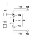
以下、図5乃至7を参照しながら、第1実施形態の記録素子基板I1について述べる。図5は、記録素子基板I1の構成の一部を示している。記録素子基板I1は、ヒータ101と、NチャネルMOS型の第1トランジスタ102及び第2トランジスタ103とをそれぞれが有する複数のユニットUを備える。ここでは、理解の容易化のため、1つのユニットUについて(ヒータ101、トランジスタ102及びトランジスタ103を、それぞれ1つずつ)示している。
(First embodiment)
Hereinafter, the recording element substrate I 1 of the first embodiment will be described with reference to FIGS. Figure 5 shows a configuration of a part of the recording element substrate I 1. The recording element substrate I 1 includes a plurality of units U each having a
ヒータ101は、記録媒体に対して記録を行うための記録素子として機能する。ヒータ101が駆動されて発熱することによって前述のノズルからインクが吐出される。具体的には、ヒータ101の両端に電圧が印加され、ヒータ101に電流が流れることにより、ヒータ101は発熱する。トランジスタ102は、ゲート端子に定電圧が供給されることでソースフォロアとして動作する。これによって、トランジスタ102はヒータ101に定電流を供給する。トランジスタ103のゲート端子に制御信号が入力される。トランジスタ103は、当該制御信号に応答してヒータ101に供給する電流を制御する。トランジスタ102及び103は、いずれも同じ導電型のMOS型のトランジスタである。
The
トランジスタ102及び103並びにヒータ101は、ノード104とノード106との間に配されている。トランジスタ102及び103がNチャネル型のトランジスタの場合、トランジスタ102は、電源ノード104とヒータ101の第1端子n1との間に電流経路を形成するように配される。そして、トランジスタ103は、接地ノード106とヒータ101の第2端子n2との間に電流経路を形成するように配されうる。なお、電源ノード104には、電源用の電極105を介して電源電圧が供給され、接地ノード106は、GND用の電極107を介して接地される。電極105、107は、それぞれ、外部からの電圧が供給されるパッド部であってもよい。電極105−電極107間の電位差Vhは、例えば32[V]である。
The
一方で、トランジスタ102及び103がPチャネル型のトランジスタの場合、103がNチャネルMOS型のトランジスタの場合と比べ電位が逆転する。つまり、トランジスタ102は、接地ノード104とヒータ101の第1端子n1との間に電流経路を形成するように配され、トランジスタ103は、電源ノード106とヒータ101の第2端子n2との間に電流経路を形成するように配されうる。なお、接地ノード104には、GND用の電極105を介して接地され、電源ノード106は、電源用の電極107を介して電源電圧が供給さる。以下、トランジスタ102及び103がNチャネル型のトランジスタの場合について記載する。
On the other hand, when the
トランジスタ102のゲート端子には、電源供給部108により一定の電圧Vghが供給される。電圧Vghは、例えば28[V]である。電源供給部108は、電源ノード104−接地ノード106間の電位差にかかわらず、トランジスタ102のゲート端子に電圧Vghを供給しうる。このような構成により、トランジスタ102はソースフォロワ型を形成している。よって、トランジスタ102のソース電位(即ち、端子n1の電位)は、記録を行うことにより生じうる電源ノード104及び接地ノード106の電位変動の影響を受けにくい。電圧Vghは、好適には、トランジスタ102のドレイン端子の電圧に対して、トランジスタ102の閾値電圧分以上に低い。つまり、トランジスタ102は飽和領域で動作することが好ましい。また、トランジスタ102のドレイン端子に電圧が供給されている間は、電源供給部108が連続的に電圧Vghを供給する。つまり、トランジスタ102のゲート端子への電圧供給が、トランジスタ102のドレイン端子への電圧の供給と同期しておこなわれる。なお、トランジスタ102は、詳細は後述するが、ソース端子とバックゲート端子(バルク)とが電気的に接続されている。
A constant voltage Vgh is supplied to the gate terminal of the
一方、トランジスタ103のゲート端子には、制御部109からの制御信号が入力される。当該制御信号の電位の変化の幅Vglは、例えば5[V]であり、0〜5[V]の範囲内で変化しうる。制御部109は、公知の論理回路やバッファ回路を用いて、5V電源系の電源で動作するように構成されればよい。このような構成により、トランジスタ103はソース接地型を形成しており、当該制御信号に応答してヒータ101を駆動しうる。例えば、トランジスタ103のゲート電位が5[V]のときは、トランジスタ103が導通状態になり、ヒータ101が駆動される(ヒータ101が通電されて発熱する)。一方、当該ゲート電位が0[V]のときは、トランジスタ103は非導通状態であり、ヒータ101は駆動されない。
On the other hand, a control signal from the
なお、Vh、Vgh及びVglの間にはVgl<Vgh<Vh(以下、第1式)の関係が成立している。好適には、トランジスタ103は非飽和領域で動作する。これによって、トランジスタ103は、トランジスタ102により供給される定電流を律速しないように構成される。
Note that a relationship of Vgl <Vgh <Vh (hereinafter referred to as the first expression) is established among Vh, Vgh, and Vgl. Preferably,
以上、上述の構成によると、記録素子基板I1は、トランジスタ102によりヒータ101に定電流が供給されるため、記録を行うに際して電源ラインの電位変動による影響を受けにくく、記録素子基板I1の動作面において有利である。また、この構成によると、記録素子基板I1の設計において、駆動トランジスタの状態を切り替える設計と、駆動トランジスタの制御端子に一定の電圧を供給する設計とを個別に考慮して行うことができる。具体的には、例えば、電源供給部108と制御部109とを個別に設計することができる。電源供給部108は、ヒータ101の端子n1の電位を固定して、ヒータ101に定電流が供給されるように設計されればよい。また、制御部109は、トランジスタ103のゲート電位Vglが所望の範囲内で変化し、その変化が所望の周波数に追従できるように設計されればよい。よって、本実施形態の構成によると、記録素子基板I1の動作設計が容易になり、記録素子基板I1の設計面においても有利である。
As described above, according to the above-described configuration, the recording element substrate I 1 is supplied with a constant current to the
なお、電源ノード104および接地ノード106の配線抵抗は、それぞれ、可能な限り低いことが望ましい。しかし、記録素子基板I1のサイズを小さく作製するために電源ノード104及び接地ノード106が配置される領域には面積的な制限がある。この場合、接地ノード106の配線抵抗を、電源ノード104の配線抵抗より低くすることが望ましい。電源ノード104と接地ノード106を同一の配線層で形成する場合は、接地ノード106の配線幅が、電源ノード104の配線幅はより広いことが望ましい。これにより、上述の構成による、電源ノードの104の配線抵抗による電源ラインの電位変動の影響を受けにくくなることに加え、接地ノード106の配線抵抗が低くなることから接地ラインの電位変動を低くすることが可能となる。
It is desirable that the wiring resistances of
図6は、上述のトランジスタ102及び103の断面構成の例を模式的に示している。トランジスタ102及び103には、高耐圧トランジスタの1つの例であるDMOSトランジスタ(Double−Diffused MOSFET)が用いられうる。図6(a)は、トランジスタ102に対応する第1のDMOSトランジスタの断面構成を例示している。図6(b)は、トランジスタ103に対応する第2のDMOSトランジスタの断面構成を例示している。図6(a)及び(b)において、端子Sはソース端子に対応し、端子Dはドレイン端子に対応し、端子Gはゲート端子に対応し、端子BGはバックゲート端子に対応している。
FIG. 6 schematically illustrates an example of a cross-sectional configuration of the
上述のDMOSトランジスタは、公知の半導体製造プロセスを用いて形成されうる。ここでは図6(a)の第1のDMOSトランジスタ(トランジスタ102)を例に用いて、その製造方法を述べる。まず、P型半導体領域10を有する半導体基板が準備され、イオン注入法により、P型半導体領域10にN型ウェル3が形成され、当該N型ウェル3の中にP型ウェル2が形成されうる。N型ウェル3は、P型ウェル2を取り囲むようにP型半導体領域10に設けられ、P型ウェル2とP型半導体領域10とを電気的に分離している。次に、半導体基板の上にゲート絶縁膜及びフィールド酸化膜1が形成され、当該ゲート絶縁膜及びフィールド酸化膜1の上の所望の領域にゲート電極6が形成されうる。その後、イオン注入法により、P型ウェル2の中にN型半導体領域4sが形成され、N型ウェル3の中にN型半導体領域4dが形成され、また、P型ウェル2の中にP型半導体領域5が形成されうる。
The above-described DMOS transistor can be formed using a known semiconductor manufacturing process. Here, a manufacturing method thereof will be described using the first DMOS transistor (transistor 102) in FIG. 6A as an example. First, a semiconductor substrate having a P-
上述のウェル、半導体領域及びゲート電極によって第1のDMOSトランジスタ(トランジスタ102)が構成されている。N型半導体領域4dは第1のドレイン領域に対応し、N型半導体領域4sは第1のソース領域に対応し、P型半導体領域5は第1のP型拡散領域に対応する。また、P型ウェル2には、P型半導体領域5に電源を供給することによって電位が与えられ、ゲート電極6に活性化信号が供給されたときにP型ウェル2にN型チャネルが形成される。
A first DMOS transistor (transistor 102) is configured by the above-described well, semiconductor region, and gate electrode. The N-
また、前述のとおり、トランジスタ102は、ソース端子とバックゲート端子とが電気的に接続されている。トランジスタ102のゲート端子には、上述の例によると、28[V]が印加されるため、バックゲート端子を0[V]に固定すると、P型半導体領域2(電位0[V])との間でゲート絶縁膜の絶縁破壊をもたらしうる。そこで、トランジスタ102が図6(a)に例示された構成を採ることにより、ソース端子Sとバックゲート端子BGとを電気的に接続しつつP型ウェル2とP型半導体領域10とを電気的に分離することができる。この構成によると、上述のゲート絶縁膜の絶縁破壊が防止されうる。
As described above, in the
一方、図6(b)の第2のDMOSトランジスタ(トランジスタ103)は、P型ウェル2’とN型ウェル3’とが側面で互いに接するように形成されている点で、図6(a)の第1のDMOSトランジスタとは構造が異なる。トランジスタ103は、P型ウェル2’とP型半導体領域10とが電気的に分離されなくてもよいため、図6(b)に例示された構成を採っており、図6(a)の構造を採る場合よりも小さい面積で形成されうる。
On the other hand, the second DMOS transistor (transistor 103) of FIG. 6B is formed such that the P-type well 2 ′ and the N-type well 3 ′ are in contact with each other on the side surface, as shown in FIG. The first DMOS transistor has a different structure. The
なお、本実施形態では、トランジスタ102及び103として、横型のDMOSトランジスタの構造を例示したが、本発明の目的を逸脱しない範囲内で、他の構造の高耐圧トランジスタが用いられてもよい。
In the present embodiment, the structure of the lateral DMOS transistor is exemplified as the
また、電源供給部108は、所望の定電圧が得られればよく、公知の回路構成を採ればよい。図7は、電源供給部108の回路構成を例示している。電源供給部108は、抵抗素子R1、R2及びR3、並びにトランジスタM1及びM2を用いて構成されている。電源供給部108には、外部から電源電圧VHTが供給されうる。電源供給部108は、抵抗素子R1〜R3の抵抗値やトランジスタM1及びM2のサイズを調節して、出力電圧Vghが所望の値になるように設計することができる。
The
(第2実施形態)
図8を参照しながら、第2実施形態の記録素子基板I2について述べる。第1実施形態では、ヒータ101に定電流を供給するための1つのトランジスタ102に対して、ヒータ101と、ヒータ101の駆動制御を行うためのトランジスタ103とが1つずつ配された構成を例示した。しかしながら、本発明は、この構成に限られるものではなく、図8に例示される記録素子基板I2の複数のユニットUのそれぞれが、1つのトランジスタ102、複数のヒータ101及び複数のトランジスタ103を含んで構成されてもよい。
(Second Embodiment)
The recording element substrate I 2 of the second embodiment will be described with reference to FIG. The first embodiment exemplifies a configuration in which one
複数のトランジスタ103のそれぞれは、前述の図6(b)に例示されたDMOSトランジスタの構造を採りうる。ここで、複数のトランジスタ103のそれぞれは、N型半導体領域4sをソース領域として共有するように設けられうる。これにより、複数のトランジスタ103は、前述の図6(a)に例示されたDMOSトランジスタの構造を採る場合よりも小さい面積で形成されうる。一方、各トランジスタ103は、他のトランジスタ103との動作上の短絡を防止するため、他のトランジスタ103とは独立にドレイン領域やゲート電極を有する。
Each of the plurality of
以上、本実施形態によると、第1実施形態と同様に、記録素子基板I2の動作面及び設計面において有利であり、さらに、複数の記録素子の駆動制御を行うための複数のトランジスタ103を小さい面積で形成することができる。
As described above, according to the present embodiment, similarly to the first embodiment, it is advantageous in terms of operation and design of the recording element substrate I 2 , and further includes a plurality of
(第3実施形態)
図9を参照しながら、第3実施形態の記録素子基板I3について述べる。記録素子基板I3の複数のユニットUのそれぞれは、図9に例示されるように、グループG(G1〜GN)を形成しており、時分割駆動方式で動作しうる。具体的には、制御部109は、各グループGにおける各ヒータ101が時分割駆動方式で駆動されるように、各トランジスタ103のゲート端子に制御信号を出力しうる。より具体的には、制御部109は、例えば、いずれのグループGを選択するかを決定する信号と、各グループGにおけるいずれのヒータ101を駆動するかを決定する信号とを出力する。
(Third embodiment)
A recording element substrate I 3 according to the third embodiment will be described with reference to FIG. Each of the plurality of units U of the recording element substrate I 3 forms a group G (G 1 to G N ) as illustrated in FIG. 9, and can operate in a time-division drive system. Specifically, the
この構成により、ヒータ101が駆動されることにより生じる熱エネルギーの隣接ヒータ101への影響が低減されうる。各グループGの1つのヒータ101が駆動される場合には、最大でN個のヒータ101が同時に駆動されうるため、電源ノード104及び接地ノード106の電位変動が顕著になりうる。しかしながら、前述のとおり、トランジスタ102のゲート端子には電源供給部108から定電圧が供給されており、各ヒータ101に流れる電流量は当該電位変動による影響を受けにくい。
With this configuration, the influence of the heat energy generated by driving the
以上、本実施形態の記録素子基板I3によっても第1〜第2実施形態と同様の効果が得られ、また、記録素子基板I3は、複数の記録素子を時分割駆動方式で駆動することにより生じうる電源の電位変動の下においても、適切に動作しうる。 As described above, the recording element substrate I 3 of the present embodiment can achieve the same effects as those of the first and second embodiments, and the recording element substrate I 3 can drive a plurality of recording elements by a time-division driving method. It is possible to operate appropriately even under potential fluctuations of the power supply that can occur due to the above.
なお、本実施形態では、最大でN個のヒータ101が同時に駆動されうるため、トランジスタ102のドレイン端子の電位が顕著に低下しうる。よって、電源供給部108から供給される定電圧Vghは、Vgl<Vgh<(Vh−(N×(N+1)/2)×ION×Rh)(以下、第2式)を満たすとよい。ここで、IONは、1つのヒータ101に流れる電流量を示し、Rhは、電源ノード104に対応するラインパターンのうちの隣接トランジスタ102間の配線抵抗を示している。なお、第2式におけるVghの上限値は、N個のヒータ101が同時に駆動された場合において、複数のトランジスタ102のうち、電源ノード104の電圧降下が最も大きいトランジスタ102のドレイン端子の電位である。例えば、Vh=32[V]、N=32、ION=100[mA]、Rh=0.1[Ω]、Vgl=5[V]とすると、第2式は、5[V]<Vgh<26.72[V]となる。また、電圧Vghは、上述の第2式を満たせばよいが、例えば粘性の高いインクを吐出する場合や吐出量を大きくする場合には、電圧Vghを、第2式を満たしつつ更に高い電圧に設定してもよい。
Note that in this embodiment, since the maximum number of
(第4実施形態)
図10を参照しながら、第4実施形態の記録素子基板I4について述べる。第3実施形態では、複数のユニットUが、時分割駆動方式で動作する複数のグループGを形成する構成を例示した。しかしながら、本発明は、この構成に限られるものではなく、例えば、図10に例示される記録素子基板I4のように、複数のグループGが2列(又は3列以上)を形成するように配列された構成でもよい。
(Fourth embodiment)
A recording element substrate I 4 of the fourth embodiment will be described with reference to FIG. In the third embodiment, a configuration in which a plurality of units U form a plurality of groups G that operate in a time-division drive method has been exemplified. However, the present invention is not limited to this configuration, for example, as the recording element substrate I 4 illustrated in FIG. 10, as a plurality of groups G to form two rows (or three or more rows) An arrangement may be used.
各列の記録素子(記録素子列)は、例えば、互いに異なる種類のインクに対応しうる。例えば、第1列目の各ヒータ101および第2列目の各ヒータ201は、例えば当該種類に対応する仕様(形状、サイズ、抵抗値等)でそれぞれ設計されうる。また、各ヒータ101に定電流を供給するトランジスタ102および各ヒータ201に定電流を供給するトランジスタ202が、当該種類に対応する仕様でそれぞれ設計されてもよい。このことは、トランジスタ103及び204、電源ライン104及び204その他の構成要素についても同様である。
The printing elements (printing element rows) in each row can correspond to different types of ink, for example. For example, each
図10では、電源用の電極105と電極205とを個別に示したが、これらは共通の電極によって設けられてもよい。このことは、GND用の電極107及び207についても同様である。また、k=1〜Nとして、第1列目の記録素子列および第2列目の記録素子列の2列において、トランジスタ103、ヒータ101、トランジスタ102は、当該2列の外側から順に配されている。当該2列の内側にトランジスタ102を配することにより、トランジスタ102のドレイン領域を当該2列の間で共有してもよい。
In FIG. 10, the
以上、本実施形態によると第1〜第3実施形態と同様の効果が得られ、また、異なる種類のインクに対応した記録素子列の設計をそれぞれ個別に行うことも可能である。 As described above, according to this embodiment, the same effects as those of the first to third embodiments can be obtained, and it is also possible to individually design printing element arrays corresponding to different types of ink.
なお、電源供給部108がトランジスタ102のゲート端子に供給する定電圧Vgh1と、電源供給部208がトランジスタ202のゲート端子に供給する定電圧Vgh2とが満たすべき条件が、前述の第2式を用いて得られうる。例えば、Vh=32[V]、N=32、ION1=100[mA]、ION2=80[mA]、Rh1=0.1[Ω]、Rh2=0.2[Ω]、Vgl=5[V]とする。ION1は、1つのヒータ101に流れる電流量を示し、Rh1は、電源ノード104に対応するラインパターンのうちの隣接トランジスタ102間の配線抵抗を示している。ION2は、1つのヒータ201に流れる電流量を示し、Rh2は、電源ノード204に対応するラインパターンのうちの隣接トランジスタ202間の配線抵抗を示している。第2式によると、5[V]<Vgh1<26.72[V]となり、5[V]<Vgh2<23.55[V]となる。このようにして、第2式の範囲内で、インクの種類に応じて電圧Vgh1及びVgh2を設定してもよい。
Note that the condition that the constant voltage Vgh1 supplied from the
以上の4つの実施形態を述べたが、本発明はこれらに限られるものではなく、目的、状態、用途及び機能その他の仕様に応じて、適宜、変更が可能であり、他の実施形態によっても為されうる。例えば、以上では、記録装置を例としてヒータを用いたインクジェット方式の構成を例示したが、本発明はこの構成に限られるものではなく、他の公知の駆動方式の記録装置にも適用されうる。また、記録の概念には、文字、図形等、有意の情報を形成する場合のみならず、無意の情報を形成する場合をも含みうる。記録媒体には、例として記録用紙を例示したが、布、プラスチックフィルム、金属板、ガラス、セラミックス、樹脂、木材、皮革等のようなインクを受容できるものであればよい。さらに、インクの概念は、一般的なインクのように、記録用紙の上に画像、模様、パターン等の形成する液体の他、例えば、インクに含まれる色剤の凝固または不溶化等のインクの処理に供される液体をも含みうる。 Although the above-described four embodiments have been described, the present invention is not limited to these, and can be appropriately changed according to the purpose, state, application, function, and other specifications. Can be done. For example, in the above description, the configuration of an ink jet system using a heater is illustrated as an example of the recording apparatus. However, the present invention is not limited to this configuration, and can be applied to recording apparatuses of other known drive systems. Further, the concept of recording can include not only the case of forming significant information such as characters and figures but also the case of forming unintended information. The recording medium is exemplified as a recording sheet as an example, but any recording medium may be used as long as it can receive ink such as cloth, plastic film, metal plate, glass, ceramics, resin, wood, leather and the like. Furthermore, the concept of ink is, as with general ink, processing of ink such as solidification or insolubilization of colorant contained in ink, in addition to liquid that forms an image, pattern, pattern, etc. on recording paper It may also contain a liquid provided to
Claims (15)
前記複数のユニットのそれぞれは、
前記記録媒体に対して記録を行うための記録素子と、
ゲート端子に電圧が供給されることによりソースフォロアとして動作し、前記記録素子に電流を供給するMOS型の第1トランジスタと、
前記第1トランジスタと同じ導電型であり、ゲート端子に入力される制御信号に応答して前記記録素子への電流の供給を制御するMOS型の第2トランジスタと、を有する、
ことを特徴とする記録素子基板。 A recording element substrate comprising a plurality of units for recording on a recording medium based on recording data,
Each of the plurality of units is
A recording element for recording on the recording medium;
A MOS-type first transistor that operates as a source follower by supplying a voltage to the gate terminal and supplies a current to the recording element;
A MOS-type second transistor that has the same conductivity type as the first transistor and controls the supply of current to the recording element in response to a control signal input to a gate terminal;
A recording element substrate.
ことを特徴とする請求項1に記載の記録素子基板。 In the first transistor, a source terminal and a back gate terminal are connected.
The recording element substrate according to claim 1.
ことを特徴とする請求項1又は請求項2に記載の記録素子基板。 The voltage supply to the gate terminal of the first transistor is performed in synchronization with the voltage supply to the drain terminal of the first transistor.
The recording element substrate according to claim 1 , wherein the recording element substrate is a recording element substrate.
前記記録素子は、第1端子と第2端子とを有し、
前記第1トランジスタは、前記第1端子と前記第1パッド部との間に電流経路を形成するように配され、
前記第2トランジスタは、前記第2端子と前記第2パッド部との間に電流経路を形成するように配され、
前記第2パッド部と前記第2トランジスタとの間の配線抵抗は、前記第1パッド部と前記第1トランジスタとの間の配線抵抗より低い、
ことを特徴とする請求項1乃至請求項3のいずれか1項に記載の記録素子基板。 The recording element substrate further includes a first pad portion to which a first external voltage is supplied, and a second pad portion to which a second external voltage is supplied.
The recording element has a first terminal and a second terminal,
The first transistor is arranged to form a current path between the first terminal and the first pad part,
The second transistor is arranged to form a current path between the second terminal and the second pad part,
A wiring resistance between the second pad portion and the second transistor is lower than a wiring resistance between the first pad portion and the first transistor;
Print element substrate according to any one of claims 1 to 3, characterized in that.
前記第1トランジスタと前記第2トランジスタとは、いずれも、Nチャネル型のトランジスタであり、
前記第1トランジスタは、前記第1端子と電源ノードとの間に電流経路を形成するように配され、
前記第2トランジスタは、前記第2端子と接地ノードとの間に電流経路を形成するように配されている、
ことを特徴とする請求項1乃至請求項3のいずれか1項に記載の記録素子基板。 The recording element has a first terminal and a second terminal,
The first transistor and the second transistor are both N-channel transistors,
The first transistor is arranged to form a current path between the first terminal and a power supply node,
The second transistor is arranged to form a current path between the second terminal and a ground node.
Print element substrate according to any one of claims 1 to 3, characterized in that.
前記第1トランジスタと前記第2トランジスタとは、いずれも、Pチャネル型のトランジスタであり、
前記第1トランジスタは、前記第1端子と接地ノードとの間に電流経路を形成するように配され、
前記第2トランジスタは、前記第2端子と電源ノードとの間に電流経路を形成するように配されている、
ことを特徴とする請求項1乃至請求項3のいずれか1項に記載の記録素子基板。 The recording element has a first terminal and a second terminal,
The first transistor and the second transistor are both P-channel transistors,
The first transistor is arranged to form a current path between the first terminal and a ground node,
The second transistor is arranged to form a current path between the second terminal and a power supply node.
Print element substrate according to any one of claims 1 to 3, characterized in that.
前記第1のDMOSトランジスタは、
半導体基板のP型半導体領域に設けられた第1のP型ウェルと、
前記第1のP型ウェルを取り囲むように前記P型半導体領域に設けられ、前記第1のP型ウェルと前記P型半導体領域とを電気的に分離する第1のN型ウェルと、
前記第1のN型ウェルの中に設けられた第1のドレイン領域と、
前記第1のP型ウェルの中に設けられた第1のソース領域と、
前記第1のドレイン領域と前記第1のソース領域との間における前記半導体基板の上に絶縁膜を介して設けられた第1のゲート電極と、
前記第1のP型ウェルの中に設けられ、前記第1のP型ウェルに電位を与えるための第1のP型拡散領域と、を含む
ことを特徴とする請求項1乃至請求項4のいずれか1項に記載の記録素子基板。 The first transistor is composed of a first DMOS transistor,
The first DMOS transistor is:
A first P-type well provided in a P-type semiconductor region of the semiconductor substrate;
A first N-type well provided in the P-type semiconductor region so as to surround the first P-type well, and electrically separating the first P-type well and the P-type semiconductor region;
A first drain region provided in the first N-type well;
A first source region provided in the first P-type well;
A first gate electrode provided on the semiconductor substrate between the first drain region and the first source region via an insulating film;
The first P-type diffusion region provided in the first P-type well and for applying a potential to the first P-type well. 5 . The recording element substrate according to claim 1.
前記第2のDMOSトランジスタは、
前記P型半導体領域に設けられた第2のP型ウェルと、
前記第2のP型ウェルの側面に接するように前記P型半導体領域に設けられた第2のN型ウェルと、
前記第2のN型ウェルの中に設けられた第2のドレイン領域と、
前記第2のP型ウェルの中に設けられた第2のソース領域と、
前記第2のドレイン領域と前記第2のソース領域との間における前記半導体基板の上に絶縁膜を介して設けられた第2のゲート電極と、
前記第2のP型ウェルの中に設けられ、前記第2のP型ウェルに電位を与えるための第2のP型拡散領域と、を含む、
ことを特徴とする請求項7に記載の記録素子基板。 The second transistor is composed of a second DMOS transistor,
The second DMOS transistor is:
A second P-type well provided in the P-type semiconductor region;
A second N-type well provided in the P-type semiconductor region so as to be in contact with a side surface of the second P-type well;
A second drain region provided in the second N-type well;
A second source region provided in the second P-type well;
A second gate electrode provided on the semiconductor substrate between the second drain region and the second source region via an insulating film;
A second P-type diffusion region provided in the second P-type well and for applying a potential to the second P-type well.
The recording element substrate according to claim 7 .
第2記録素子と、
ゲート端子に入力される制御信号に応答して前記第2記録素子への電流の供給を制御するMOS型の第3トランジスタと、をさらに有し、
前記第1トランジスタは、前記第2記録素子に電流を供給する
ことを特徴とする請求項1乃至請求項8のいずれか1項に記載の記録素子基板。 Each of the plurality of units is
A second recording element;
A MOS-type third transistor that controls supply of current to the second recording element in response to a control signal input to the gate terminal;
Wherein the first transistor includes a recording element substrate according to any one of claims 1 to 8, characterized in that for supplying a current to the second recording element.
前記第3のDMOSトランジスタは、ソース領域として、前記第2トランジスタのソース領域を共有しており、
前記第3のDMOSトランジスタは、前記第2トランジスタとは独立に、第3のN型ウェルと、前記第3のN型ウェルの中に設けられた第3のドレイン領域と、前記第3のドレイン領域と前記ソース領域との間における半導体基板の上に絶縁膜を介して設けられた第3のゲート電極と、を含む、
ことを特徴とする請求項9に記載の記録素子基板。 The third transistor is composed of a third DMOS transistor,
The third DMOS transistor shares the source region of the second transistor as a source region,
The third DMOS transistor includes, independently of the second transistor, a third N-type well, a third drain region provided in the third N-type well, and the third drain including, third gate electrode provided via an insulating film on a semi-conductor substrate that put between region and the source region,
The recording element substrate according to claim 9 .
前記第1のユニットの前記第2トランジスタ及び前記第3トランジスタと、前記第2のユニットの前記第2トランジスタ及び前記第3トランジスタとの間に、前記第1のユニット及び前記第2のユニットの前記記録素子及び前記第2記録素子が配され、
前記第1のユニットの前記記録素子及び前記第2記録素子と、前記第2のユニットの前記記録素子及び前記第2記録素子との間に、前記第1のユニット及び前記第2のユニットの前記第1トランジスタが配されている、
ことを特徴とする請求項9又は請求項10に記載の記録素子基板。 The first unit and the second unit in the plurality of units are disposed adjacent to each other,
Between the second transistor and the third transistor of the first unit and the second transistor and the third transistor of the second unit, the first unit and the second unit of the first unit. A recording element and the second recording element are arranged;
Between the recording element and the second recording element of the first unit and the recording element and the second recording element of the second unit, the first unit and the second unit A first transistor is disposed;
Recording element substrate according to claim 9 or claim 10, characterized in that.
ことを特徴とする請求項11に記載の記録素子基板。 The gate terminals of the second transistor and the third transistor are connected to the recording element and the second recording element in the first unit and the second unit, respectively, so that each of the recording element and the second recording element is driven by a time-division driving method. A control unit for outputting a control signal;
The recording element substrate according to claim 11 .
前記第2トランジスタは非飽和領域で動作する
ことを特徴とする請求項1乃至請求項12のいずれか1項に記載の記録素子基板。 The first transistor operates in a saturation region;
The recording element substrate according to any one of claims 1 to 12 , wherein the second transistor operates in a non-saturated region.
前記記録素子が駆動されたことに応答してインクを吐出する吐出口と、前記吐出口にインクを供給するインク供給部と、を有する、
ことを特徴とする記録ヘッド。 A recording element substrate according to any one of claims 1 to 13 , comprising:
An ejection port that ejects ink in response to driving of the recording element; and an ink supply unit that supplies ink to the ejection port.
A recording head characterized by that.
前記記録ヘッドを駆動する記録ヘッドドライバと、を備える、
ことを特徴とする記録装置。
A recording head according to claim 14 ;
A recording head driver for driving the recording head,
A recording apparatus.
Priority Applications (2)
| Application Number | Priority Date | Filing Date | Title |
|---|---|---|---|
| JP2013132025A JP6110738B2 (en) | 2013-06-24 | 2013-06-24 | Recording element substrate, recording head, and recording apparatus |
| US14/289,805 US9227401B2 (en) | 2013-06-24 | 2014-05-29 | Printing element substrate, printhead, and printing apparatus |
Applications Claiming Priority (1)
| Application Number | Priority Date | Filing Date | Title |
|---|---|---|---|
| JP2013132025A JP6110738B2 (en) | 2013-06-24 | 2013-06-24 | Recording element substrate, recording head, and recording apparatus |
Related Child Applications (1)
| Application Number | Title | Priority Date | Filing Date |
|---|---|---|---|
| JP2017031329A Division JP6368393B2 (en) | 2017-02-22 | 2017-02-22 | Recording element substrate, recording head, and recording apparatus |
Publications (3)
| Publication Number | Publication Date |
|---|---|
| JP2015006738A JP2015006738A (en) | 2015-01-15 |
| JP2015006738A5 JP2015006738A5 (en) | 2016-06-16 |
| JP6110738B2 true JP6110738B2 (en) | 2017-04-05 |
Family
ID=52110562
Family Applications (1)
| Application Number | Title | Priority Date | Filing Date |
|---|---|---|---|
| JP2013132025A Active JP6110738B2 (en) | 2013-06-24 | 2013-06-24 | Recording element substrate, recording head, and recording apparatus |
Country Status (2)
| Country | Link |
|---|---|
| US (1) | US9227401B2 (en) |
| JP (1) | JP6110738B2 (en) |
Families Citing this family (7)
| Publication number | Priority date | Publication date | Assignee | Title |
|---|---|---|---|---|
| JP6532262B2 (en) * | 2015-03-30 | 2019-06-19 | キヤノン株式会社 | Substrate for liquid discharge head, liquid discharge head, liquid discharge device, and liquid discharge method |
| JP6624936B2 (en) * | 2016-01-06 | 2019-12-25 | キヤノン株式会社 | Printing element substrate, liquid ejection head, and printing apparatus |
| JP6758895B2 (en) | 2016-04-22 | 2020-09-23 | キヤノン株式会社 | Liquid discharge head substrate, liquid discharge head, and recording device |
| US11667128B2 (en) | 2018-05-15 | 2023-06-06 | Hewlett-Packard Development Company, L.P. | Fluidic die with monitoring circuit fault protection structure |
| US11186086B2 (en) | 2019-04-19 | 2021-11-30 | Markem-Imaje Corporation | Systems and techniques to reduce debris buildup around print head nozzles |
| EP3956144A4 (en) * | 2019-04-19 | 2022-04-27 | Markem-Imaje Corporation | Purged ink removal from print head |
| CN113993706A (en) * | 2019-06-19 | 2022-01-28 | 惠普发展公司,有限责任合伙企业 | Control device for high-side switch of printing head |
Family Cites Families (11)
| Publication number | Priority date | Publication date | Assignee | Title |
|---|---|---|---|---|
| JP2001191531A (en) * | 2000-01-07 | 2001-07-17 | Canon Inc | Print head, method of driving the same and printer |
| JP2002355970A (en) | 2001-05-31 | 2002-12-10 | Canon Inc | Recorder |
| JP4125153B2 (en) * | 2002-02-20 | 2008-07-30 | キヤノン株式会社 | Semiconductor device and liquid ejection device using the same |
| JP4272854B2 (en) * | 2002-07-10 | 2009-06-03 | キヤノン株式会社 | Semiconductor device and liquid ejection device using the same |
| JP4194313B2 (en) * | 2002-07-23 | 2008-12-10 | キヤノン株式会社 | Recording head |
| US9283750B2 (en) * | 2005-05-20 | 2016-03-15 | Hewlett-Packard Development Company, L.P. | Constant current mode firing circuit for thermal inkjet-printing nozzle |
| JP2008091689A (en) * | 2006-10-03 | 2008-04-17 | Sharp Corp | Lateral double-diffused mos transistor, its manufacturing method, and integrated circuit |
| JP2009119714A (en) * | 2007-11-14 | 2009-06-04 | Canon Inc | Recording head and recorder |
| US8226190B2 (en) * | 2008-12-01 | 2012-07-24 | Canon Kabushiki Kaisha | Recording element substrate and recording head having the same |
| JP5677109B2 (en) * | 2010-03-01 | 2015-02-25 | キヤノン株式会社 | Inkjet recording head substrate, inkjet recording head, and recording apparatus |
| JP5425818B2 (en) * | 2011-01-12 | 2014-02-26 | 株式会社東海理化電機製作所 | Indicator drive circuit |
-
2013
- 2013-06-24 JP JP2013132025A patent/JP6110738B2/en active Active
-
2014
- 2014-05-29 US US14/289,805 patent/US9227401B2/en not_active Expired - Fee Related
Also Published As
| Publication number | Publication date |
|---|---|
| US20140375711A1 (en) | 2014-12-25 |
| JP2015006738A (en) | 2015-01-15 |
| US9227401B2 (en) | 2016-01-05 |
Similar Documents
| Publication | Publication Date | Title |
|---|---|---|
| JP6110738B2 (en) | Recording element substrate, recording head, and recording apparatus | |
| US9505211B2 (en) | Semiconductor device, liquid discharge head, liquid discharge cartridge, and liquid discharge apparatus | |
| US9022497B2 (en) | Printing element substrate, printhead, and printing apparatus | |
| JP6368393B2 (en) | Recording element substrate, recording head, and recording apparatus | |
| US9463618B2 (en) | Liquid discharge substrate, liquid discharge head, and recording device | |
| US9340022B1 (en) | Liquid discharging substrate, printhead, and printing apparatus | |
| JP6302231B2 (en) | Recording element substrate, recording head, and recording apparatus | |
| US10259216B2 (en) | Semiconductor device, liquid discharge head, liquid discharge head cartridge, and printing apparatus | |
| US9278518B2 (en) | Printhead substrate, printhead, and printing apparatus | |
| US9415584B2 (en) | Liquid discharge head substrate, liquid discharge head, and printing apparatus | |
| US9694575B2 (en) | Semiconductor device, liquid discharge head, liquid discharge cartridge, and liquid discharge apparatus | |
| JP6376829B2 (en) | Liquid ejection substrate, liquid ejection head, and recording apparatus | |
| JP2013180537A (en) | Liquid ejecting apparatus and head control circuit | |
| US10391788B2 (en) | Element substrate, printhead, and printing apparatus | |
| US9919518B2 (en) | Printing element substrate, liquid ejection head, and printing apparatus | |
| US9522529B2 (en) | Substrate for liquid ejection head, liquid ejection head, and apparatus and method for ejecting liquid | |
| US11104126B2 (en) | Liquid ejection apparatus, ejection control method, and liquid ejection head | |
| US8777356B2 (en) | Fluid discharge head semiconductor device, fluid discharge head, and fluid discharge apparatus | |
| JP2004050492A (en) | Inkjet head driving circuit | |
| JP2017013354A (en) | Liquid discharge substrate, liquid discharge head, recording device, and manufacturing method of printed matter |
Legal Events
| Date | Code | Title | Description |
|---|---|---|---|
| A521 | Request for written amendment filed |
Free format text: JAPANESE INTERMEDIATE CODE: A523 Effective date: 20160422 |
|
| A621 | Written request for application examination |
Free format text: JAPANESE INTERMEDIATE CODE: A621 Effective date: 20160422 |
|
| A977 | Report on retrieval |
Free format text: JAPANESE INTERMEDIATE CODE: A971007 Effective date: 20170207 |
|
| TRDD | Decision of grant or rejection written | ||
| A01 | Written decision to grant a patent or to grant a registration (utility model) |
Free format text: JAPANESE INTERMEDIATE CODE: A01 Effective date: 20170210 |
|
| A61 | First payment of annual fees (during grant procedure) |
Free format text: JAPANESE INTERMEDIATE CODE: A61 Effective date: 20170310 |
|
| R151 | Written notification of patent or utility model registration |
Ref document number: 6110738 Country of ref document: JP Free format text: JAPANESE INTERMEDIATE CODE: R151 |