JP6068193B2 - Reception device and transmission / reception system - Google Patents
Reception device and transmission / reception system Download PDFInfo
- Publication number
- JP6068193B2 JP6068193B2 JP2013039802A JP2013039802A JP6068193B2 JP 6068193 B2 JP6068193 B2 JP 6068193B2 JP 2013039802 A JP2013039802 A JP 2013039802A JP 2013039802 A JP2013039802 A JP 2013039802A JP 6068193 B2 JP6068193 B2 JP 6068193B2
- Authority
- JP
- Japan
- Prior art keywords
- delay
- signal
- data
- clock
- circuit
- Prior art date
- Legal status (The legal status is an assumption and is not a legal conclusion. Google has not performed a legal analysis and makes no representation as to the accuracy of the status listed.)
- Expired - Fee Related
Links
Images


Classifications
-
- H—ELECTRICITY
- H04—ELECTRIC COMMUNICATION TECHNIQUE
- H04L—TRANSMISSION OF DIGITAL INFORMATION, e.g. TELEGRAPHIC COMMUNICATION
- H04L25/00—Baseband systems
- H04L25/02—Details ; arrangements for supplying electrical power along data transmission lines
- H04L25/0264—Arrangements for coupling to transmission lines
- H04L25/0272—Arrangements for coupling to multiple lines, e.g. for differential transmission
-
- H—ELECTRICITY
- H04—ELECTRIC COMMUNICATION TECHNIQUE
- H04L—TRANSMISSION OF DIGITAL INFORMATION, e.g. TELEGRAPHIC COMMUNICATION
- H04L25/00—Baseband systems
- H04L25/02—Details ; arrangements for supplying electrical power along data transmission lines
- H04L25/14—Channel dividing arrangements, i.e. in which a single bit stream is divided between several baseband channels and reassembled at the receiver
-
- H—ELECTRICITY
- H04—ELECTRIC COMMUNICATION TECHNIQUE
- H04L—TRANSMISSION OF DIGITAL INFORMATION, e.g. TELEGRAPHIC COMMUNICATION
- H04L7/00—Arrangements for synchronising receiver with transmitter
- H04L7/0008—Synchronisation information channels, e.g. clock distribution lines
-
- H—ELECTRICITY
- H04—ELECTRIC COMMUNICATION TECHNIQUE
- H04L—TRANSMISSION OF DIGITAL INFORMATION, e.g. TELEGRAPHIC COMMUNICATION
- H04L7/00—Arrangements for synchronising receiver with transmitter
- H04L7/0016—Arrangements for synchronising receiver with transmitter correction of synchronization errors
- H04L7/0033—Correction by delay
- H04L7/0037—Delay of clock signal
-
- H—ELECTRICITY
- H04—ELECTRIC COMMUNICATION TECHNIQUE
- H04L—TRANSMISSION OF DIGITAL INFORMATION, e.g. TELEGRAPHIC COMMUNICATION
- H04L7/00—Arrangements for synchronising receiver with transmitter
- H04L7/0016—Arrangements for synchronising receiver with transmitter correction of synchronization errors
- H04L7/0033—Correction by delay
- H04L7/0041—Delay of data signal
-
- H—ELECTRICITY
- H04—ELECTRIC COMMUNICATION TECHNIQUE
- H04L—TRANSMISSION OF DIGITAL INFORMATION, e.g. TELEGRAPHIC COMMUNICATION
- H04L7/00—Arrangements for synchronising receiver with transmitter
- H04L7/02—Speed or phase control by the received code signals, the signals containing no special synchronisation information
- H04L7/033—Speed or phase control by the received code signals, the signals containing no special synchronisation information using the transitions of the received signal to control the phase of the synchronising-signal-generating means, e.g. using a phase-locked loop
- H04L7/0337—Selecting between two or more discretely delayed clocks or selecting between two or more discretely delayed received code signals
- H04L7/0338—Selecting between two or more discretely delayed clocks or selecting between two or more discretely delayed received code signals the correction of the phase error being performed by a feed forward loop
-
- H—ELECTRICITY
- H04—ELECTRIC COMMUNICATION TECHNIQUE
- H04L—TRANSMISSION OF DIGITAL INFORMATION, e.g. TELEGRAPHIC COMMUNICATION
- H04L7/00—Arrangements for synchronising receiver with transmitter
- H04L7/04—Speed or phase control by synchronisation signals
Description
本発明は、受信装置及び送受信システムに関し、特に、クロック信号とデータ信号とを別の配線で送信する送受信システム、及び、それに用いられる受信装置に関する。 The present invention relates to a reception device and a transmission / reception system, and more particularly to a transmission / reception system that transmits a clock signal and a data signal through different wirings, and a reception device used therefor.
送信装置から受信装置にデータを送信する送受信システムで用いられるデータ通信方式の一つは、クロック信号とデータ信号とを別の配線で送信する方式である。例えば、MIPI規格(Mobile Industry Processor Interface)による通信(例えば、MIPI DSIやMIPI D−PHY)は、このようなデータ通信方式に対応している。MIPI D−PHYは、例えば、パネル表示装置のドライバICへの高速データ通信に用いられており、近年の表示パネルの高解像度化に伴い、MIPI−D−PHYによるデータ通信において、更なる高速化が要求されている。 One of the data communication methods used in a transmission / reception system that transmits data from a transmission device to a reception device is a method in which a clock signal and a data signal are transmitted using different wirings. For example, communication (for example, MIPI DSI and MIPI D-PHY) based on the MIPI standard (Mobile Industry Processor Interface) corresponds to such a data communication method. MIPI D-PHY is used for, for example, high-speed data communication to a driver IC of a panel display device, and further increases in data communication by MIPI-D-PHY with the recent increase in resolution of display panels. Is required.
クロック信号とデータ信号とを別の配線で送信するデータ通信方式において、通信速度を増大させる上での一つの問題は、クロック信号とデータ信号との間でスキューが発生することである。高速通信においてはスキューの問題は非常に重大な問題になり得る。例えば、MIPI D−PHY規格に準拠した送受信システムにおいて1.5Gbpsの通信速度で通信する場合のスキューの許容値は、数十〜数百psと非常に小さい。 In a data communication system in which a clock signal and a data signal are transmitted through different wirings, one problem in increasing the communication speed is that a skew occurs between the clock signal and the data signal. In high-speed communication, the problem of skew can be a very serious problem. For example, in a transmission / reception system compliant with the MIPI D-PHY standard, the allowable skew value when communicating at a communication speed of 1.5 Gbps is very small, such as several tens to several hundreds ps.
スキューを解消するための技術は、例えば、特開平5−110550号公報、特開平10−164037号公報、及び、特開2004−236019号公報に知られている。しかしながら、発明者の検討によれば、これらの技術においては、スキューの解消において改良の余地がある。 Techniques for eliminating the skew are known, for example, in JP-A-5-110550, JP-A-10-164037, and JP-A-2004-236019. However, according to studies by the inventors, there is room for improvement in the elimination of skew in these techniques.
したがって、本発明の目的は、クロック信号とデータ信号とを別の配線で送信する送受信システムにおいて、スキューを解消するための技術を提供することにある。 Therefore, an object of the present invention is to provide a technique for eliminating a skew in a transmission / reception system that transmits a clock signal and a data signal through different wirings.
本発明の一の観点では、受信装置が、外部クロック信号を受け取ってクロック信号を出力する第1受信部と、外部データ信号を受け取ってデータ信号を出力する第2受信部と、クロック信号とデータ信号の少なくとも一方の信号を遅延することにより遅延調整後クロック信号及び遅延調整後データ信号とを生成するように構成された可変遅延回路と、遅延調整後クロック信号に同期して遅延調整後データ信号をラッチして出力データ信号を生成するラッチ回路部と、スキュー検出回路とを具備する。スキュー検出回路は、データ信号又はデータ信号を遅延して得られる遅延データ信号によって伝送される特定データ列を、クロック信号からの遅延時間が異なる第1〜第Nクロック信号(Nは、2以上の整数)に同期してラッチすることでスキュー検出データを生成し、スキュー検出データに応じて、該少なくとも一方の信号が可変遅延回路において遅延される遅延時間を制御する。 In one aspect of the present invention, a receiving device receives an external clock signal and outputs a clock signal, a second receiving unit that receives an external data signal and outputs a data signal, a clock signal and data A variable delay circuit configured to generate a delay-adjusted clock signal and a delay-adjusted data signal by delaying at least one of the signals, and a delay-adjusted data signal in synchronization with the delay-adjusted clock signal Are latched to generate an output data signal, and a skew detection circuit. The skew detection circuit converts a data signal or a specific data sequence transmitted by a delayed data signal obtained by delaying the data signal into first to Nth clock signals (N is 2 or more) with different delay times from the clock signal. The skew detection data is generated by latching in synchronization with an integer), and the delay time in which the at least one signal is delayed in the variable delay circuit is controlled according to the skew detection data.
本発明の他の観点では、受信装置が、外部クロック信号を受け取ってクロック信号を出力する第1受信部と、外部データ信号を受け取ってデータ信号を出力する第2受信部と、クロック信号とデータ信号の少なくとも一方の信号を遅延することにより遅延調整後クロック信号及び遅延調整後データ信号とを生成する可変遅延回路と、遅延調整後クロック信号に同期して遅延調整後データ信号をラッチして出力データ信号を生成するラッチ回路部と、スキュー検出回路とを具備する。スキュー検出回路は、データ信号からの遅延時間が異なる第1〜第Nデータ信号(Nは、2以上の整数)によって伝送される特定データ列をクロック信号又はクロック信号を遅延して得られる遅延クロック信号に同期してラッチすることでスキュー検出データを生成し、スキュー検出データに応じて、該少なくとも一方の信号が遅延される遅延時間を制御する。 In another aspect of the present invention, the receiving device receives a first clock signal that receives an external clock signal and outputs a clock signal, a second receiver unit that receives the external data signal and outputs a data signal, and the clock signal and data A variable delay circuit that generates a delay-adjusted clock signal and a delay-adjusted data signal by delaying at least one of the signals, and latches and outputs the delay-adjusted data signal in synchronization with the delay-adjusted clock signal A latch circuit unit that generates a data signal and a skew detection circuit are provided. The skew detection circuit is a delayed clock obtained by delaying a clock signal or a clock signal from a specific data string transmitted by first to Nth data signals (N is an integer of 2 or more) having different delay times from the data signal. Skew detection data is generated by latching in synchronization with the signal, and a delay time for delaying at least one of the signals is controlled according to the skew detection data.
本発明の更に他の観点では、送受信システムが、送信装置と、送信装置から外部クロック信号及び外部データ信号を受け取る受信装置とを具備する。該受信装置は、上述の構成を有している。一実施形態では、送信装置から受信装置への外部クロック信号及び外部データ信号への伝送が、MIPI D−PHY規格に準拠して行われる。この場合、該特定データ列は、HY−SYNCコードに含まれるデータ列であることが好ましい。 In still another aspect of the present invention, a transmission / reception system includes a transmission device and a reception device that receives an external clock signal and an external data signal from the transmission device. The receiving apparatus has the above-described configuration. In one embodiment, the transmission from the transmitting device to the receiving device to the external clock signal and the external data signal is performed according to the MIPI D-PHY standard. In this case, the specific data string is preferably a data string included in the HY-SYNC code.
本発明によれば、クロック信号とデータ信号とを別の配線で送信する送受信システムにおいて、スキューを解消する技術が提供される。 ADVANTAGE OF THE INVENTION According to this invention, the technique which eliminates a skew is provided in the transmission / reception system which transmits a clock signal and a data signal by another wiring.
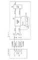
図1は、本実施形態の一実施形態の送受信システムの構成を示すブロック図である。当該送受信システムは、トランスミッタ(送信装置)1とレシーバ(受信装置)2とを備えている。トランスミッタ1とレシーバ2とは、伝送線路3、4を介して接続されている。トランスミッタ1は、レシーバ2に、データ信号DATA及びクロック信号CLOCKを、それぞれ、伝送線路3、4を介して送信する。本実施形態では、トランスミッタ1からレシーバ2へのデータ信号DATA及びクロック信号CLOCKの送信は、MIPI D−PHY規格に準拠して行われる。
FIG. 1 is a block diagram showing a configuration of a transmission / reception system according to an embodiment of the present invention. The transmission / reception system includes a transmitter (transmitting device) 1 and a receiver (receiving device) 2. The
トランスミッタ1は、送信側アンプ11、12を備えており、レシーバ2は、受信側アンプ21、22を備えている。送信側アンプ11、12としては、いずれも、高速アンプが使用される。トランスミッタ1の送信側アンプ11は、データ信号DATAを、伝送線路3を介してレシーバ2に送信する第1の送信部として機能する。トランスミッタ1の送信側アンプ12は、クロック信号CLOCKを、伝送線路4を介してレシーバ2の受信側アンプ22に送信する第2の送信部として機能する。伝送線路3、4においては、データ信号DATA、クロック信号CLOCKは、いずれも、差動小振幅信号として伝送される。
The
レシーバ2は、受信側アンプ21、22は、それぞれ、差動小振幅信号としてトランスミッタ1から伝送されたデータ信号DATA(外部データ信号)及びクロック信号CLOCK(外部クロック信号)を受け取り、受け取ったデータ信号DATA、クロック信号CLOCKをシングルエンド信号に変換する受信部として機能する。即ち、受信側アンプ21、22から出力されるデータ信号DATA、クロック信号CLOCKは、いずれも、シングルエンド信号である。受信側アンプ21、22としては、いずれも、高速アンプが使用される。ここで、レシーバ2の受信側アンプ21から出力されるデータ信号DATAは、クロック信号CLOCKの半周期に1ビットのデータを伝送する信号である。即ち、データ信号DATAは、クロック信号CLOCKの各エッジ(立ち上がりエッジ及び立ち下がりエッジの両方を含む)あたり、1ビットのデータを含んでいることになる。
The
レシーバ2は、更に、可変遅延回路23と、ラッチ回路24と、スキュー検出回路25とを備えている。可変遅延回路23は、受信側アンプ21、22から出力されたデータ信号DATAとクロック信号CLOCKの間の相対的な遅延を調節する回路であり、その一方の信号を他方の信号に対して、特定の遅延時間だけ遅延させる機能を有している。ここで、当該遅延時間は、スキュー検出回路25から供給される遅延制御信号SCTRLに応じて調節される。図1において、可変遅延回路23によって遅延が調節されたデータ信号DATAとクロック信号CLOCKは、それぞれ、遅延調整後データ信号DATAADJ、遅延調整後クロック信号CLOCKADJとして図示されている。
The
ラッチ回路24は、遅延調整後クロック信号CLOCKADJに同期して遅延調整後データ信号DATAADJをラッチし、出力データ信号DOUTを生成する。本実施形態では、ラッチ回路24は、遅延調整後クロック信号CLOCKADJの立ち上がりエッジと立ち下がりエッジとの両方に応答して遅延調整後データ信号DATAADJをラッチする。
The
スキュー検出回路25は、データ信号DATAとクロック信号CLOCKの間のスキューを検出し、検出されたスキューに応じて遅延制御信号SCTRLを生成する。生成された遅延制御信号SCTRLは、可変遅延回路23に送られる。可変遅延回路23においては、スキューに応じて生成された遅延制御信号SCTRLに応答して、データ信号DATAとクロック信号CLOCKの間の相対的な遅延が制御されることになる。
The
本実施形態では、スキュー検出回路25におけるスキューの検出は、データ信号DATAによって、特定のデータ列が特定のタイミングでレシーバ2に送られると判明しているという前提で行われる。そして、スキュー検出回路25では、該特定のデータ列を、クロック信号CLOCKから生成された多相クロック信号に同期してラッチして得られる一群のデータ(以下、「スキュー検出データ」という。)を用いてスキューが検出される。
In the present embodiment, the skew detection in the
トランスミッタ1からレシーバ2へのデータ通信が、MIPI D−PHY規格に準拠して行われる本実施形態では、HS−SYNCコードに含まれる特定のデータ列を、多相クロック信号に同期してラッチすることにより、スキュー検出データが生成される。図2は、HS−SYNCコードを説明する図である。HS−SYNCコードは、8ビットからなるシリアルコードであり、その値は、MIPI D−PHY規格において、“00011101”と定められている。HS−SYNCコードは、MIPI D−PHY規格において、トランスミッタ1からレシーバ2へのデータ通信がLP(low power)モードからHS(high speed)モードに切り換えられるときに、データ信号DATAで送られるデータ列の先頭に挿入されると規定されている。これは、レシーバ2にとって、HS−SYNCコードが送られるタイミングは既知であることを意味している
In this embodiment in which data communication from the
HS−SYNCコードにはデータ列“01110”が存在しており、本実施形態では、該データ列の1番目“1”と3番目の“1”(図2において、破線の楕円で示されている)が、スキュー検出データに利用される。データ信号DATAにおいて、クロック信号CLOCKの半周期あたりに1ビットが送信される本実施形態では、データ信号DATAとクロック信号CLOCKの間のタイミングが正常であれば、該データ列“01110”の1番目“1”と3番目の“1”は、その両方が、クロック信号CLOCKの立ち下がりエッジでラッチされるか、クロック信号CLOCKの立ち上がりエッジでラッチされるかのいずれでなければならない。そして、データ信号DATAとクロック信号CLOCKの間のスキューが全く存在しない場合には、クロック信号CLOCKと位相が少し異なるクロック信号の立ち下がりエッジ又は立ち上がりエッジで該データ列“01110”をラッチしても、該データ列“01110”の1番目“1”と3番目の“1”が正常にラッチできるはずである。その一方で、データ信号DATAとクロック信号CLOCKの間にスキューが存在する場合には、クロック信号CLOCKと位相が少し異なるクロック信号の立ち下がりエッジ又は立ち上がりエッジで該データ列“01110”をラッチすると、1番目“1”又は3番目の“1”が正常にラッチできず、データ“0”がラッチされることになる。これは、クロック信号CLOCKから生成された多相クロック信号の立ち下がりエッジ又は立ち上がりエッジで該データ列“01110”をラッチして得られるデータ、即ち、スキュー検出データを参照することにより、スキューを検出できることを意味している。ここで、スキュー検出データを得るために用いられる多相クロック信号は、クロック信号CLOCKと同一の周波数を有しており、且つ、互いに位相が異なるように生成される。 A data string “01110” exists in the HS-SYNC code. In this embodiment, the first “1” and the third “1” of the data string (indicated by broken-line ellipses in FIG. 2). Is used for skew detection data. In this embodiment, in which one bit is transmitted per half cycle of the clock signal CLOCK in the data signal DATA, if the timing between the data signal DATA and the clock signal CLOCK is normal, the first of the data string “01110” Both “1” and the third “1” must be either latched on the falling edge of the clock signal CLOCK or latched on the rising edge of the clock signal CLOCK. If there is no skew between the data signal DATA and the clock signal CLOCK, the data string “01110” may be latched at the falling edge or the rising edge of the clock signal that is slightly different in phase from the clock signal CLOCK. The first “1” and the third “1” of the data string “01110” should be able to be latched normally. On the other hand, if there is a skew between the data signal DATA and the clock signal CLOCK, the data string “01110” is latched at the falling edge or the rising edge of the clock signal that is slightly different in phase from the clock signal CLOCK. The first “1” or the third “1” cannot be latched normally, and the data “0” is latched. This is because the skew is detected by referring to the data obtained by latching the data string “01110” at the falling edge or the rising edge of the multiphase clock signal generated from the clock signal CLOCK, that is, the skew detection data. It means you can do it. Here, the multiphase clock signal used to obtain the skew detection data has the same frequency as the clock signal CLOCK and is generated so that the phases are different from each other.
図3は、本実施形態の送受信システムの動作を示しており、特に、HS−SYNCコードに含まれるデータ列“01110”を、クロック信号CLOCKから生成された多相クロック信号CLOCK#0〜#2の立ち下がりエッジに同期してラッチすることにより得られるスキュー検出データを図示している。多相クロック信号CLOCK#0〜#2は、データ信号DATAにおいてデータ列“01110”が転送される時間帯に、それぞれ、2つの立ち下がりエッジを含んでいる。以下では、2つの立ち下がりエッジのうち、時間的に前の立ち下がりエッジを「前側立ち下がりエッジ」、時間的に後ろの立ち下がりエッジを「後側立ち下がりエッジ」ということにする。
FIG. 3 shows the operation of the transmission / reception system of the present embodiment. In particular, the data sequence “01110” included in the HS-SYNC code is generated from the multiphase clock signals
一例としては、図3(a)に示されているように、データ信号DATAとクロック信号CLOCKの間のタイミングが正常である場合、多相クロック信号CLOCK#0〜#2の前側立ち下がりエッジに同期してデータ列“01110”の1番目の“1”がラッチされ、後側立ち下がりエッジに同期して3番目の“1”がラッチされる。この結果、得られるスキュー検出データは、全て“1”となる。
As an example, as shown in FIG. 3A, when the timing between the data signal DATA and the clock signal CLOCK is normal, the front falling edge of the multiphase clock signals
また、図3(b)に示されているように、データ信号DATAに対してクロック信号CLOCKのタイミングが遅延するようなスキューが発生している場合、位相が相対的に遅い多相クロック信号(図3(b)ではクロック信号CLOCK#1、#2)の、後側立ち下がりエッジに同期してラッチすることで得られるスキュー検出データが“0”になる。データ信号DATAに対するクロック信号CLOCKのタイミングの遅延が増大すると、“0”として得られるスキュー検出データの数も増大する。
Further, as shown in FIG. 3B, when there is a skew that delays the timing of the clock signal CLOCK with respect to the data signal DATA, a multiphase clock signal (with a relatively slow phase) ( In FIG. 3B, the skew detection data obtained by latching the clock signals
更に、図3の(c)に示されているように、クロック信号CLOCKに対してデータ信号DATAのタイミングが遅延するようなスキューが発生している場合、位相が相対的に進んでいる多相クロック信号(図3(c)ではクロック信号CLOCK#0、#1)の、前側立ち下がりエッジに同期してラッチすることで得られるスキュー検出データが“0”になる。クロック信号CLOCKに対するデータ信号DATAのタイミングの遅延が増大すると、“0”として得られるスキュー検出データの数も増大する。
Further, as shown in FIG. 3C, when there is a skew that delays the timing of the data signal DATA with respect to the clock signal CLOCK, the phase is relatively advanced. The skew detection data obtained by latching the clock signal (clock signals
このように、“0”のスキュー検出データの存在により、スキューの発生を検出することができる。また、“0”のスキュー検出データが、前側立ち上がりエッジ、後側立ち上がりエッジのいずれで生じるかにより、スキューの向き(即ち、データ信号DATAとクロック信号CLOCKのいずれが遅れているか)を判別することができる。更に、“0”のスキュー検出データの数により、スキューの程度を判別することができる。このようにして生成されたスキュー検出データに応じて遅延制御信号SCTRLを生成し、データ信号DATAとクロック信号CLOCKの間の相対的なタイミングを遅延制御信号SCTRLに応答して制御することで、データ信号DATAとクロック信号CLOCKの間のスキューを解消することができる。 Thus, the occurrence of skew can be detected by the presence of skew detection data of “0”. Further, the skew direction (that is, which of the data signal DATA and the clock signal CLOCK is delayed) is determined depending on whether the skew detection data “0” is generated at the front rising edge or the rear rising edge. Can do. Further, the degree of skew can be determined from the number of skew detection data of “0”. A delay control signal S CTRL is generated according to the skew detection data generated in this way, and the relative timing between the data signal DATA and the clock signal CLOCK is controlled in response to the delay control signal S CTRL. The skew between the data signal DATA and the clock signal CLOCK can be eliminated.
なお、データ信号DATAとクロック信号CLOCKの間のタイミングが、図3(a)〜(c)のような関係となる多相クロック信号CLOCK#0〜#2は、クロック信号CLOCKを適宜の遅延時間で遅延することで生成することができることに留意されたい。
Note that the multiphase clock signals
ここで、データ信号DATAの代わりに、データ信号DATAを遅延して得られる遅延データ信号DATADLYを多相クロック信号CLOCK#0〜#2に同期してラッチすることで、スキュー検出データを取得しても良い。データ信号DATAの代わりに、それを遅延して得られる遅延データ信号DATADLYを用いても、スキュー検出データの値が相違し得るだけであり、本質的な相違は無い。この場合でも、スキュー検出データから遅延制御信号SCTRLを生成するロジックを必要に応じて変更することで、適正な遅延制御信号SCTRLを生成することができる。
Here, instead of the data signal DATA, the delayed data signal DATA DLY obtained by delaying the data signal DATA is latched in synchronization with the multiphase clock signals
図3では、3個の多相クロック信号CLOCK#0〜#2がスキュー検出データの生成に用いられているが、多相クロック信号の数は、3には限定されない。図4に示されているように、HS−SYNCコードに含まれるデータ列“01110”を、N個の多相クロック信号CLOCK#0〜#(N−1)(Nは、2以上の整数)に同期してラッチすることによってスキュー検出データを生成してもよい。
In FIG. 3, three multiphase clock signals
また、データ信号DATA(又は遅延データ信号DATADLY)を多相クロック信号CLOCK#0〜#(N−1)でラッチしてスキュー検出データを生成する代わりに、図5に図示されているように、データ信号DATAからの遅延時間が異なる複数のデータ信号DATA#0〜#(N−1)を生成し、そのそれぞれを、クロック信号CLOCKに同期してラッチすることによってスキュー検出データを生成してもよい。図5では、3つのデータ信号#0〜#2が生成される場合が図示されている。この場合でも、スキュー検出データによって、スキューの検出が可能である。
Further, instead of latching the data signal DATA (or the delayed data signal DATA DLY ) with the multiphase clock signals
例えば、図5(a)に示されているように、データ信号DATAとクロック信号CLOCKの間のタイミングが正常である場合、データ信号#0〜#2の全てにおいて、データ列“01110”の1番目の“1”がクロック信号CLOCKの前側立ち下がりエッジに同期してラッチされ、3番目の“1”が後側立ち下がりエッジに同期してラッチされる。この結果、得られるスキュー検出データは、全て“1”となる。 For example, as shown in FIG. 5A, when the timing between the data signal DATA and the clock signal CLOCK is normal, 1 of the data string “01110” is present in all of the data signals # 0 to # 2. The third “1” is latched in synchronization with the front falling edge of the clock signal CLOCK, and the third “1” is latched in synchronization with the rear falling edge. As a result, the obtained skew detection data is all “1”.
また、図5(b)に示されているように、データ信号DATAに対してクロック信号CLOCKのタイミングが遅延するようなスキューが発生している場合、データ信号#0〜#2のうち、位相が相対的に進んでいるデータ信号(図5(b)ではデータ信号#0、#1)をクロック信号CLOCKの後側立ち下がりエッジに同期してラッチすることで得られるスキュー検出データが“0”になる。データ信号DATAに対するクロック信号CLOCKのタイミングの遅延が増大すると、“0”として得られるスキュー検出データの数も増大する。 Further, as shown in FIG. 5B, when a skew is generated such that the timing of the clock signal CLOCK is delayed with respect to the data signal DATA, the phase of the data signals # 0 to # 2 is increased. The skew detection data obtained by latching the data signal (data signals # 0 and # 1 in FIG. 5B) in synchronization with the trailing edge of the clock signal CLOCK is “0”. "become. When the delay of the timing of the clock signal CLOCK with respect to the data signal DATA increases, the number of skew detection data obtained as “0” also increases.
更に、図5(c)に示されているように、クロック信号CLOCKに対してデータ信号DATAのタイミングが遅延するようなスキューが発生している場合、データ信号#0〜#2のうち、位相が相対的に遅れているデータ信号(図5(c)ではデータ信号#1、#2)をクロック信号CLOCKの前側立ち下がりエッジに同期してラッチすることで得られるスキュー検出データが“0”になる。クロック信号CLOCKに対するデータ信号DATAのタイミングの遅延が増大すると、“0”として得られるスキュー検出データの数も増大する。 Further, as shown in FIG. 5C, when there is a skew that delays the timing of the data signal DATA with respect to the clock signal CLOCK, the phase of the data signals # 0 to # 2 The skew detection data obtained by latching the data signals (data signals # 1 and # 2 in FIG. 5C) in synchronization with the front falling edge of the clock signal CLOCK are “0”. become. When the delay of the timing of the data signal DATA with respect to the clock signal CLOCK increases, the number of skew detection data obtained as “0” also increases.
このように、遅延時間が異なる複数のデータ信号DATA#0〜#(N−1)をクロック信号CLOCKに同期してラッチすることによってスキュー検出データを生成する場合についても、“0”のスキュー検出データの存在により、スキューの発生を検出することができる。
As described above, even when the skew detection data is generated by latching a plurality of data signals
上述の実施形態では、HS−SYNCコードに含まれるデータ列“01110”が、スキュー検出データの生成に利用されるが、HS−SYNCコードに含まれる他のデータ列をスキュー検出データの生成に用いても良い。図6Aは、HS−SYNCコードに含まれるデータ列“0011”を用いてスキュー検出データを生成する場合を示している。 In the above-described embodiment, the data sequence “01110” included in the HS-SYNC code is used for generating skew detection data, but another data sequence included in the HS-SYNC code is used for generating skew detection data. May be. FIG. 6A shows a case where skew detection data is generated using a data string “0011” included in the HS-SYNC code.
図6A(a)に示されているように、データ信号DATAとクロック信号CLOCKの間のタイミングが正常である場合、多相クロック信号CLOCK#0〜#2の特定の立ち上がりエッジに同期してデータ列“0011”の2番目の“0”がラッチされ、該立ち上がりエッジに続く立ち下がりエッジに同期して1番目の“1”がラッチされる。この結果、立ち上がりエッジに同期して得られるスキュー検出データは全て“0”となり、立ち下がりエッジに同期して得られるスキュー検出データは全て“1”となる。
As shown in FIG. 6A (a), when the timing between the data signal DATA and the clock signal CLOCK is normal, the data is synchronized with a specific rising edge of the multiphase clock signals
また、図6A(b)に示されているように、データ信号DATAに対してクロック信号CLOCKのタイミングが遅延するようなスキューが発生している場合、多相クロック信号CLOCK#0〜#2のうち、位相が進んだ多相クロック信号CLOCK#0の特定の立ち上がりエッジに同期してラッチすることで得られるスキュー検出データが“0”になるのに対し、位相が遅いクロック信号(図6A(b)では、多相クロック信号CLOCK#1、#2)の、当該特定立ち上がりエッジに対応する立ち上がりエッジに同期してラッチすることで得られるスキュー検出データが“1”になる。データ信号DATAに対するクロック信号CLOCKのタイミングの遅延が増大すると、“1”として得られるスキュー検出データの数も増大する。
Further, as shown in FIG. 6A (b), when there is a skew that delays the timing of the clock signal CLOCK with respect to the data signal DATA, the multi-phase clock signals
更に、図6Aの(c)に示されているように、クロック信号CLOCKに対してデータ信号DATAのタイミングが遅延するようなスキューが発生している場合、多相クロック信号CLOCK#0〜#2のうち位相が遅い多相クロック信号CLOCK#2の特定の立ち下がりエッジに同期してラッチすることで得られるスキュー検出データが“1”になるのに対し、位相が進んだクロック信号(図6A(c)では、多相クロック信号CLOCK#0、#1)の、当該特定立ち下がりエッジに対応する立ち下がりエッジに同期してラッチすることで得られるスキュー検出データが“0”になる。クロック信号CLOCKに対するデータ信号DATAのタイミングの遅延が増大すると、“0”として得られるスキュー検出データの数も増大する。
Further, as shown in (c) of FIG. 6A, when a skew is generated such that the timing of the data signal DATA is delayed with respect to the clock signal CLOCK, the multiphase clock signals
このように、HS−SYNCコードのデータ列“0011”を用いてスキュー検出データを生成する場合についても、スキュー検出データの値からスキューの発生を検出することができる。 As described above, even when the skew detection data is generated using the data string “0011” of the HS-SYNC code, the occurrence of the skew can be detected from the value of the skew detection data.
また、図6Bは、HS−SYNCコードに含まれるデータ列“1101”を用いてスキュー検出データを生成する場合を示している。 FIG. 6B shows a case where skew detection data is generated using the data string “1101” included in the HS-SYNC code.
図6B(a)に示されているように、データ信号DATAとクロック信号CLOCKの間のタイミングが正常である場合、多相クロック信号CLOCK#0〜#2の特定の立ち下がりエッジに同期してデータ列“1100”の2番目の“1”がラッチされ、該立ち下がりエッジに続く立ち上がりエッジに同期して1番目の“0”がラッチされる。この結果、立ち上がりエッジに同期して得られるスキュー検出データは全て“1”となり、立ち下がりエッジに同期して得られるスキュー検出データは全て“0”となる。
As shown in FIG. 6B (a), when the timing between the data signal DATA and the clock signal CLOCK is normal, it is synchronized with a specific falling edge of the multiphase clock signals
また、図6B(b)に示されているように、データ信号DATAに対してクロック信号CLOCKのタイミングが遅延するようなスキューが発生している場合、多相クロック信号CLOCK#0〜#2のうち、位相が進んだ多相クロック信号CLOCK#0の特定立ち上がりエッジに同期してラッチすることで得られるスキュー検出データが“1”になり、該特定立ち上がりエッジに続く立ち下がりエッジ(特定立ち下がりエッジ)に同期してラッチすることで得られるスキュー検出データが“0”になる。一方、位相が遅い多相クロック信号CLOCK#1、#2の当該特定立ち上がりエッジに対応する立ち上がりエッジに同期してラッチすることで得られるスキュー検出データは“1”になり、多相クロック信号CLOCK#1、#2の該特定立ち下がりエッジに対応する立ち下がりエッジに同期してラッチすることで得られるスキュー検出データは“0”になる。
Further, as shown in FIG. 6B (b), when there is a skew that delays the timing of the clock signal CLOCK with respect to the data signal DATA, the multi-phase clock signals
更に、図6A(c)に示されているように、クロック信号CLOCKに対してデータ信号DATAのタイミングが遅延するようなスキューが発生している場合、多相クロック信号CLOCK#0〜#2のうち位相が遅い多相クロック信号CLOCK#2の特定立ち上がりエッジに同期してラッチすることで得られるスキュー検出データが“0”になるのに対し、位相が進んだクロック信号(図6B(c)では、多相クロック信号CLOCK#0、#1)の、当該特定立ち上がりエッジに対応する立ち上がりエッジに同期してラッチすることで得られるスキュー検出データが“1”になる。クロック信号CLOCKに対するデータ信号DATAのタイミングの遅延が増大すると、“1”として得られるスキュー検出データの数も増大する。
Furthermore, as shown in FIG. 6A (c), when there is a skew that delays the timing of the data signal DATA with respect to the clock signal CLOCK, the multiphase clock signals
このように、HS−SYNCコードのデータ列“1101”を用いてスキュー検出データを生成する場合についても、スキュー検出データの値からスキューの発生を検出することができる。 As described above, even when the skew detection data is generated using the data string “1101” of the HS-SYNC code, the occurrence of the skew can be detected from the value of the skew detection data.
図3〜図5、図6A、図6Bから理解されるように、一般に、スキュー検出データは、値が既知である任意のデータ列をラッチすることで生成することができる。ただし、多相クロック信号CLOCK#0〜#(N−1)、又は、クロック信号CLOCKに含まれるエッジのうち、立ち下がりエッジ又は立ち上がりエッジの一方のみに同期してスキュー検出データを生成することが好適である。図3、図4には、多相クロック信号CLOCK#0〜#(N−1)の立ち下がりエッジのみに同期してスキュー検出データを生成する場合が図示されており、図5には、クロック信号CLOCKの立ち下がりエッジのみに同期してスキュー検出データを生成する場合が図示されていることに留意されたい。図6A、図6Bに示されているように、スキュー検出データの生成において、立ち上がりエッジと立ち下がりエッジの両方を用いると、立ち上がりエッジに同期してデータ信号DATA(又は、データ信号#0〜#(N−1))をラッチする回路と、立ち下がりエッジに同期してデータ信号DATA(又は、データ信号#0〜#(N−1))をラッチする回路の両方が必要となる。これは、回路規模を増大させるため好ましくない。多相クロック信号CLOCK#0〜#(N−1)、又は、クロック信号CLOCKに含まれるエッジのうち、立ち下がりエッジ又は立ち上がりエッジの一方のみに同期してスキュー検出データを生成する構成(図3〜図5の動作を行う構成)では、スキュー検出データの生成に用いられる回路の回路規模を小さくすることができる。
As can be understood from FIGS. 3 to 5, 6 </ b> A, and 6 </ b> B, generally, skew detection data can be generated by latching an arbitrary data string having a known value. However, the skew detection data may be generated in synchronization with only one of the falling edge and the rising edge among the edges included in the multiphase clock signals
なお、データ信号DATA及びクロック信号CLOCKの送信がMIPI D−PHY規格以外の規格で行われる場合においても、特定のタイミングでレシーバ2に送られることが既知である特定のデータ列を、クロック信号CLOCKから生成された多相クロック信号に同期してラッチすることでスキュー検出データを生成することができることに留意されたい。
Even when the transmission of the data signal DATA and the clock signal CLOCK is performed according to a standard other than the MIPI D-PHY standard, a specific data string that is known to be sent to the
また、図7に図示されているように、可変遅延回路23において多相クロック信号CLOCK#0〜#(N−1)が生成され、且つ、スキュー検出回路25において多相クロック信号CLOCK#0〜#(N−1)がスキュー検知データの生成に用いられる場合には、可変遅延回路23からスキュー検出回路25に多相クロック信号CLOCK#0〜#(N−1)が供給されてもよい。この場合、スキュー検出回路25において多相クロック信号CLOCK#0〜#(N−1)が生成されない。このような構成は、可変遅延回路23から出力される遅延調整後クロック信号CLOCKADJが多相クロック信号CLOCK#0〜#(N−1)から選択される場合に有効である。
Further, as shown in FIG. 7, the multi-phase clock signals
同様に、図8に図示されているように、可変遅延回路23においてデータ信号DATA#0〜#(N−1)が生成され、且つ、スキュー検出回路25においてデータ信号DATA#0〜#(N−1)がスキュー検知データの生成に用いられる場合には、可変遅延回路23からスキュー検出回路25にデータ信号DATA#0〜#(N−1)が供給されてもよい。この場合、スキュー検出回路25においてデータ信号DATA#0〜#(N−1)が生成されない。このような構成は、可変遅延回路23から出力される遅延調整後データ信号DATAADJがデータ信号DATA#0〜#(N−1)から選択される場合に有効である。
Similarly, as shown in FIG. 8, the data signals
更に、図9に図示されているように、可変遅延回路23においてデータ信号DATAを遅延して遅延データ信号DATADLYが生成され、且つ、スキュー検出回路25においてスキュー検知データの生成に遅延データ信号DATADLYが用いられる場合、可変遅延回路23からスキュー検出回路25に遅延データ信号DATADLYが供給されてもよい。なお、可変遅延回路23からスキュー検出回路25に遅延データ信号DATADLYが供給される構成は、図7においても図示されていることに留意されたい。
Further, as shown in FIG. 9, the delay data signal DATA DLY is generated by delaying the data signal DATA in the
同様に、図10に示されているように、可変遅延回路23においてクロック信号CLOCKを遅延して遅延クロック信号CLOCKDLYが生成され、且つ、スキュー検出回路25においてスキュー検知データの生成に遅延クロック信号CLOCKDLYが用いられる場合、可変遅延回路23からスキュー検出回路25に遅延クロック信号CLOCKDLYが供給されてもよい。
Similarly, as shown in FIG. 10, the delay clock signal CLOCK DLY is generated by delaying the clock signal CLOCK in the
以下では、上記の実施形態の具体的な実施例、特に、可変遅延回路23、ラッチ回路24及びスキュー検出回路25の具体的な実施例について説明する。
Hereinafter, specific examples of the above-described embodiment, particularly, specific examples of the
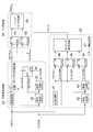
図11は、実施例1における可変遅延回路23と、ラッチ回路24と、スキュー検出回路25の構成を示すブロック図である。図11に図示された回路構成は、図1に図示されている可変遅延回路23、ラッチ回路24及びスキュー検出回路25の具体的な実施例である。
FIG. 11 is a block diagram illustrating the configuration of the
実施例1においては、可変遅延回路23は、遅延回路31〜33と、選択回路34とを備えている。遅延回路31は、データ信号DATAを遅延して遅延調整後データ信号DATAADJを生成する。本実施例では、遅延回路31の遅延時間は固定である。
In the first embodiment, the
遅延回路32、33及び選択回路34は、スキュー検出回路25から供給される遅延制御信号SCTRLに応答して、クロック信号CLOCKを遅延した信号である遅延調整後クロック信号CLOCKADJを生成するクロック可変遅延部23Bを構成している。詳細には、遅延回路32、33は、クロック信号CLOCKから多相クロック信号CLOCK#0〜#2を生成する回路部分である。本実施形態では、可変遅延回路23に入力されるクロック信号CLOCKが、そのまま、クロック信号CLOCK#0として用いられる。遅延回路32は、クロック信号CLOCK#0を遅延してクロック信号CLOCK#1を生成する。遅延回路33は、クロック信号CLOCK#1を遅延してクロック信号CLOCK#2を生成する。選択回路34は、遅延制御信号SCTRLに応答して、多相クロック信号CLOCK#0〜#2のいずれかを選択し、選択したクロック信号を遅延調整後クロック信号CLOCKADJとして出力する。
The
ラッチ回路24は、Dフリップフロップ51、52と、デシリアライザ(deserializer)回路53とを備えている。Dフリップフロップ51は、遅延調整後データ信号DATAADJを、遅延調整後クロック信号CLOCKADJの立ち上がりエッジに同期してラッチする。一方、Dフリップフロップ52は、遅延調整後データ信号DATAADJを、遅延調整後クロック信号CLOCKADJの立ち下がりエッジに同期してラッチする。デシリアライザ回路53は、Dフリップフロップ51、52から出力されるデータに対してデシリアライズ処理を行い、出力データ信号DOUTを生成する。このような構成のラッチ回路24では、遅延調整後クロック信号CLOCKADJの立ち上がりエッジ及び立ち下がりエッジの両方に同期して、遅延調整後データ信号DATAADJをラッチすることに留意されたい。
The
スキュー検出回路25は、遅延回路41〜43と、Dフリップフロップ44〜46と、タイミング検出回路47とを備えている。遅延回路41は、データ信号DATAを遅延して遅延データ信号DATADLYを生成する。遅延回路42、43は、クロック信号CLOCKから多相クロック信号CLOCK#0〜#2を生成する回路部分である。本実施形態では、スキュー検出回路25に入力されるクロック信号CLOCKが、そのまま、クロック信号CLOCK#0として用いられる。遅延回路42は、クロック信号CLOCK#0を遅延してクロック信号CLOCK#1を生成する。遅延回路43は、クロック信号CLOCK#1を遅延してクロック信号CLOCK#2を生成する。
The
Dフリップフロップ44〜46は、それぞれ、多相クロック信号CLOCK#0〜#2の立ち下がりエッジに同期して遅延データ信号DATADLYをラッチする。Dフリップフロップ44〜46から出力されるデータが、スキュー検出データとして用いられる。
The D flip-
タイミング検出回路47は、Dフリップフロップ44〜46から出力されるスキュー検出データに応じて、遅延制御信号SCTRLを生成する。本実施例では、遅延制御信号SCTRLは、可変遅延回路23の選択回路34に、多相クロック信号CLOCK#0〜#2のいずれか選択すべきかを指定する信号として生成される。タイミング検出回路47には、スキュー検出データの値から、多相クロック信号CLOCK#0〜#2のいずれかを選択するロジックが組み込まれる。
The
実施例1の可変遅延回路23の遅延回路31〜33、及び、スキュー検出回路25の遅延回路41〜43は、いずれも、「実質的に」同一な遅延時間Cを有している。ここで、「実質的に」とは、製造時に不可避的に発生するバラツキを無視することを意味している。
The
図12は、実施例1におけるスキュー検出回路25の動作を示すタイミングチャートである。図12(a)に示されているように、データ信号DATAとクロック信号CLOCKの間のタイミングが正常である場合、多相クロック信号CLOCK#0〜#2の前側立ち下がりエッジに同期して遅延データ信号DATADLYのデータ列“01110”の1番目の“1”がラッチされ、後側立ち下がりエッジに同期して3番目の“1”がラッチされる。この結果、得られるスキュー検出データは、全て“1”となる。この場合、スキュー検出回路25から可変遅延回路23に送られる遅延制御信号SCTRLは、スキュー検出データに応じ、中間的な位相を有する多相クロック信号CLOCK#1を選択するように生成される。このような動作により、ラッチ回路24のDフリップフロップ51、52の動作タイミングのマージンを大きくすることができる。
FIG. 12 is a timing chart illustrating the operation of the
また、図12(b)に示されているように、データ信号DATAに対してクロック信号CLOCKのタイミングが遅延するようなスキューが発生している場合、遅延データ信号DATADLYのデータ列“01110”を、位相が遅い多相クロック信号(図12(b)ではクロック信号CLOCK#1、#2)の後側立ち下がりエッジに同期してラッチすることで得られるスキュー検出データが“0”になる。この場合、スキュー検出回路25から可変遅延回路23に送られる遅延制御信号SCTRLは、スキュー検出データに応じ、位相が相対的に進んだ多相クロック信号CLOCK#0を選択するように生成される。このような動作により、ラッチ回路24のDフリップフロップ51、52の動作タイミングのマージンを大きくすることができる。
Also, as shown in FIG. 12B, when there is a skew that delays the timing of the clock signal CLOCK with respect to the data signal DATA, the data string “01110” of the delayed data signal DATA DLY. Is detected in synchronism with the trailing edge of the multiphase clock signal with a slow phase (clock signals
更に、図12(c)に示されているように、クロック信号CLOCKに対してデータ信号DATAのタイミングが遅延するようなスキューが発生している場合、位相が進んだ多相クロック信号(図12(c)ではクロック信号CLOCK#0、#1)の、前側立ち下がりエッジに同期してラッチすることで得られるスキュー検出データが“0”になる。この場合、スキュー検出回路25から可変遅延回路23に送られる遅延制御信号SCTRLは、スキュー検出データに応じ、位相が相対的に遅れた多相クロック信号CLOCK#2を選択するように生成される。このような動作により、ラッチ回路24のDフリップフロップ51、52の動作タイミングのマージンを大きくすることができる。
Further, as shown in FIG. 12C, when there is a skew that delays the timing of the data signal DATA with respect to the clock signal CLOCK, the multiphase clock signal with the advanced phase (FIG. 12). In (c), the skew detection data obtained by latching the clock signals
いずれの場合でも、本実施例では、遅延データ信号DATADLYのデータ列“01110”を多相クロック信号CLOCK#0〜#2の立ち下がりエッジに同期してラッチすることで得られるスキュー検出データに応じて遅延制御信号SCTRLが生成され、その遅延制御信号SCTRLにより、可変遅延回路23の選択回路34が制御される。これにより、遅延調整後データ信号DATAADJと遅延調整後クロック信号CLOCKADJの間の相対的な遅延が最適に調整され、遅延調整後データ信号DATAADJと遅延調整後クロック信号CLOCKADJの間のスキューを小さくすることができる。
In any case, in this embodiment, the skew detection data obtained by latching the data string “01110” of the delayed data signal DATA DLY in synchronization with the falling edges of the multiphase clock signals
図13は、実施例2における可変遅延回路23と、ラッチ回路24と、スキュー検出回路25の構成を示すブロック図である。図13に図示された回路構成は、図9に図示されている可変遅延回路23、ラッチ回路24及びスキュー検出回路25の具体的な実施例である。
FIG. 13 is a block diagram illustrating the configuration of the
図13に図示されている実施例2における回路構成は、図11に図示されている実施例1の回路構成と類似している。相違点は、実施例2の回路構成では、スキュー検出回路25から遅延回路41が除去されると共に可変遅延回路23からスキュー検出回路25に遅延データ信号DATADLYが供給されることである。可変遅延回路23の遅延回路31から出力される遅延調整後データ信号DATAADJが、スキュー検出回路25に供給される遅延データ信号DATADLYとしても使用される。スキュー検出回路25に供給された遅延データ信号DATADLYは、Dフリップフロップ44〜46に供給される。
The circuit configuration in the second embodiment illustrated in FIG. 13 is similar to the circuit configuration in the first embodiment illustrated in FIG. 11. The difference is that the
図13に図示されている実施例2の回路構成によれば、実施例1の回路構成と比較して遅延回路の数を減少させることができる。なお、実施例2における可変遅延回路23と、ラッチ回路24と、スキュー検出回路25の動作は、実施例1と同様であり、説明を省略する。
According to the circuit configuration of the second embodiment illustrated in FIG. 13, the number of delay circuits can be reduced as compared with the circuit configuration of the first embodiment. The operations of the
図14は、実施例3における可変遅延回路23と、ラッチ回路24と、スキュー検出回路25の構成を示すブロック図である。図14に図示された回路構成は、図7に図示されている可変遅延回路23、ラッチ回路24及びスキュー検出回路25の具体的な実施例である。
FIG. 14 is a block diagram illustrating the configuration of the
図14に図示されている実施例3における回路構成は、図13に図示されている実施例2の回路構成と類似している。相違点は、実施例3の回路構成では、スキュー検出回路25から遅延回路42、43が除去されると共に、可変遅延回路23からスキュー検出回路25に多相クロック信号CLOCK#0〜#2が供給されることである。遅延回路32から出力されるクロック信号CLOCK#1は、選択回路34に加え、スキュー検出回路25のDフリップフロップ45に供給される。また、遅延回路33から出力されるクロック信号CLOCK#2は、選択回路34に加え、スキュー検出回路25のDフリップフロップ46に供給される。ここで、実施例3では、クロック信号CLOCKが、そのままクロック信号#0として使用されることに留意されたい。
The circuit configuration in the third embodiment illustrated in FIG. 14 is similar to the circuit configuration in the second embodiment illustrated in FIG. The difference is that in the circuit configuration of the third embodiment, the
図14に図示されている実施例3の回路構成によれば、実施例2の回路構成と比較して、遅延回路の数を一層に減少させることができる。なお、実施例3における可変遅延回路23と、ラッチ回路24と、スキュー検出回路25の動作は、実施例1と同様であり、説明を省略する。
According to the circuit configuration of the third embodiment illustrated in FIG. 14, the number of delay circuits can be further reduced as compared with the circuit configuration of the second embodiment. The operations of the
図15は、実施例4における可変遅延回路23と、ラッチ回路24と、スキュー検出回路25の構成を示すブロック図である。図15に図示された回路構成は、図1に図示されている可変遅延回路23、ラッチ回路24及びスキュー検出回路25の他の実施例である。
FIG. 15 is a block diagram illustrating configurations of the
実施例4においては、可変遅延回路23は、遅延回路61、52と、選択回路63と、遅延回路64とを備えている。遅延回路61、62及び選択回路63は、スキュー検出回路25から供給される遅延制御信号SCTRLに応答して、データ信号DATAを遅延した信号である遅延調整後データ信号DATAADJを生成するデータ可変遅延部23Aを構成している。詳細には、遅延回路61、62は、データ信号DATAからの遅延時間が互いに異なるデータ信号DATA#0〜#2を生成する回路部分である。本実施形態では、可変遅延回路23に入力されるデータ信号DATAが、そのまま、データ信号DATA#0として用いられる。遅延回路61は、データ信号DATA#0を遅延してデータ信号DATA#1を生成する。遅延回路62は、データ信号DATA#1を遅延してデータ信号DATA#2を生成する。選択回路63は、遅延制御信号SCTRLに応答して、データ信号DATA#0〜#2のいずれかを選択し、選択したデータ信号を遅延調整後データ信号DATAADJとして出力する。遅延回路64は、クロック信号CLOCKを遅延して遅延調整後クロック信号CLOCKADJを生成する。本実施例では、遅延回路64の遅延時間は固定である。
In the fourth embodiment, the
実施例4のラッチ回路24の構成は、実施例1乃至3のラッチ回路24と同様である。詳細には、実施例4のラッチ回路24は、Dフリップフロップ51、52と、デシリアライザ回路53とを備えている。Dフリップフロップ51は、遅延調整後データ信号DATAADJを、遅延調整後クロック信号CLOCKADJの立ち上がりエッジに同期してラッチする。一方、Dフリップフロップ52は、遅延調整後データ信号DATAADJを、遅延調整後クロック信号CLOCKADJの立ち下がりエッジに同期してラッチする。デシリアライザ回路53は、Dフリップフロップ51、52から出力されるデータに対してデシリアライズ処理を行い、出力データ信号DOUTを生成する。このような構成のラッチ回路24では、遅延調整後クロック信号CLOCKADJの立ち上がりエッジ及び立ち下がりエッジの両方に同期して、遅延調整後データ信号DATAADJをラッチすることに留意されたい。
The configuration of the
また、実施例4では、スキュー検出回路25が、遅延回路71〜73と、Dフリップフロップ74〜76と、タイミング検出回路77とを備えている。遅延回路71、72は、データ信号DATAからデータ信号DATA#0〜#2を生成する回路部分である。本実施形態では、スキュー検出回路25に入力されるデータ信号DATAが、そのまま、データ信号DATA#0として用いられる。遅延回路71は、データ信号DATA#0を遅延してデータ信号DATA#1を生成する。遅延回路72は、データ信号DATA#1を遅延してデータ信号DATA#2を生成する。一方、遅延回路73は、クロック信号CLOCKを遅延して遅延クロック信号CLOCKDLYを生成する。
In the fourth embodiment, the
Dフリップフロップ74〜76は、それぞれ、遅延クロック信号CLOCKDLYの立ち下がりエッジに同期してデータ信号DATA#0〜#2をラッチする。Dフリップフロップ74〜76から出力されるデータが、スキュー検出データとして用いられる。
The D flip-
タイミング検出回路77は、Dフリップフロップ74〜76から出力されるスキュー検出データに応じて、遅延制御信号SCTRLを生成する。本実施例では、遅延制御信号SCTRLは、可変遅延回路23の選択回路34に、データ信号DATA#0〜#2のいずれか選択すべきかを指定する信号として生成される。タイミング検出回路77には、スキュー検出データの値から、データ信号DATA#0〜#2のいずれかを選択するロジックが組み込まれる。
The
実施例4の可変遅延回路23の遅延回路61〜63、及び、スキュー検出回路25の遅延回路71〜73の遅延時間は、「実質的に」同一である。ここで、「実質的に」とは、製造時に不可避的に発生するバラツキを無視することを意味している。
The delay times of the
図16は、実施例4におけるスキュー検出回路25の動作を示すタイミングチャートである。図16(a)に示されているように、データ信号DATAとクロック信号CLOCKの間のタイミングが正常である場合、遅延クロック信号CLOCKDLYの前側立ち下がりエッジに同期してデータ信号DATA#0〜#2のデータ列“01110”の1番目の“1”がラッチされ、後側立ち下がりエッジに同期して3番目の“1”がラッチされる。この結果、得られるスキュー検出データは、全て“1”となる。この場合、スキュー検出回路25から可変遅延回路23に送られる遅延制御信号SCTRLは、スキュー検出データに応じて、中間的な遅延を有するデータ信号DATA#1を選択するように生成される。このような動作により、ラッチ回路24のDフリップフロップ51、52の動作タイミングのマージンを大きくすることができる。
FIG. 16 is a timing chart illustrating the operation of the
また、図16(b)に示されているように、データ信号DATAに対してクロック信号CLOCKのタイミングが遅延するようなスキューが発生している場合、データ信号#0〜#2のうちデータ信号DATAからの遅延時間が相対的に小さいデータ信号(図16(b)では、データ信号#0、#1)を遅延クロック信号CLOCKDLYの後側立ち下がりエッジに同期してラッチすることで得られるスキュー検出データが“0”になる。この場合、スキュー検出回路25から可変遅延回路23に送られる遅延制御信号SCTRLは、スキュー検出データに応じて、データ信号DATAからの相対的に遅延時間が大きいデータ信号DATA#2を選択するように生成される。このような動作により、ラッチ回路24のDフリップフロップ51、52の動作タイミングのマージンを大きくすることができる。
Further, as shown in FIG. 16B, when a skew is generated such that the timing of the clock signal CLOCK is delayed with respect to the data signal DATA, the data signal among the data signals # 0 to # 2 is displayed. It is obtained by latching data signals (data signals # 0 and # 1 in FIG. 16B) having a relatively small delay time from DATA in synchronization with the trailing edge of the delayed clock signal CLOCK DLY. The skew detection data becomes “0”. In this case, the delay control signal S CTRL sent from the
更に、図16(c)に示されているように、クロック信号CLOCKに対してデータ信号DATAのタイミングが遅延するようなスキューが発生している場合、データ信号DATAからの遅延時間が相対的に大きいデータ信号(図16(c)ではデータ信号DATA#2)の、前側立ち下がりエッジに同期してラッチすることで得られるスキュー検出データが“0”になる。この場合、スキュー検出回路25から可変遅延回路23に送られる遅延制御信号SCTRLは、スキュー検出データに応じて、データ信号DATAからの相対的に遅延時間が小さいデータ信号DATA#0を選択するように生成される。このような動作により、ラッチ回路24のDフリップフロップ51、52の動作タイミングのマージンを大きくすることができる。
Further, as shown in FIG. 16C, when a skew occurs that delays the timing of the data signal DATA with respect to the clock signal CLOCK, the delay time from the data signal DATA is relatively set. The skew detection data obtained by latching the large data signal (data signal
いずれの場合でも、本実施例では、データ信号DATA#0〜#2のデータ列“01110”を遅延クロック信号CLOCKDLYの立ち下がりエッジに同期してラッチすることで得られるスキュー検出データに応じて遅延制御信号SCTRLが生成され、その遅延制御信号SCTRLにより、可変遅延回路23の選択回路63が制御される。これにより、遅延調整後データ信号DATAADJと遅延調整後クロック信号CLOCKADJの間の相対的な遅延が最適に調整され、遅延調整後データ信号DATAADJと遅延調整後クロック信号CLOCKADJの間のスキューを小さくすることができる。
In any case, according to the present embodiment, according to the skew detection data obtained by latching the data string “01110” of the data signals
図17は、実施例5における可変遅延回路23と、ラッチ回路24と、スキュー検出回路25の構成を示すブロック図である。図17に図示された回路構成は、図10に図示されている可変遅延回路23、ラッチ回路24及びスキュー検出回路25の具体的な実施例である。
FIG. 17 is a block diagram illustrating configurations of the
図17に図示されている実施例5における回路構成は、図15に図示されている実施例4の回路構成と類似している。相違点は、実施例5の回路構成では、スキュー検出回路25から遅延回路73が除去されると共に可変遅延回路23からスキュー検出回路25に遅延クロック信号CLOCKDLYが供給されることである。可変遅延回路23の遅延回路64から出力される遅延調整後クロック信号CLOCKADJが、スキュー検出回路25に供給される遅延クロック信号CLOCKDLYとしても使用される。スキュー検出回路25に供給された遅延クロック信号CLOCKDLYは、Dフリップフロップ74〜76に供給される。
The circuit configuration in the fifth embodiment illustrated in FIG. 17 is similar to the circuit configuration in the fourth embodiment illustrated in FIG. The difference is that the
図17に図示されている実施例5の回路構成によれば、実施例4の回路構成と比較して遅延回路の数を減少させることができる。なお、実施例5における可変遅延回路23と、ラッチ回路24と、スキュー検出回路25の動作は、実施例4と同様であり、説明を省略する。
According to the circuit configuration of the fifth embodiment illustrated in FIG. 17, the number of delay circuits can be reduced as compared with the circuit configuration of the fourth embodiment. The operations of the
図18は、実施例6における可変遅延回路23と、ラッチ回路24と、スキュー検出回路25の構成を示すブロック図である。図18に図示された回路構成は、図8に図示されている可変遅延回路23、ラッチ回路24及びスキュー検出回路25の具体的な実施例である。
FIG. 18 is a block diagram illustrating the configuration of the
図18に図示されている実施例6における回路構成は、図17に図示されている実施例5の回路構成と類似している。相違点は、実施例6の回路構成では、スキュー検出回路25から遅延回路71、72が除去されると共に、可変遅延回路23からスキュー検出回路25にデータ信号#0〜#2が供給されることである。遅延回路61から出力されるデータ信号DATA#1は、選択回路63に加え、スキュー検出回路25のDフリップフロップ75に供給される。また、遅延回路62から出力されるデータ信号DATA#2は、選択回路63に加え、スキュー検出回路25のDフリップフロップ76に供給される。ここで、実施例6では、データ信号DATAが、そのままデータ信号#0として使用されることに留意されたい。
The circuit configuration in the sixth embodiment illustrated in FIG. 18 is similar to the circuit configuration in the fifth embodiment illustrated in FIG. The difference is that in the circuit configuration of the sixth embodiment, the
図18に図示されている実施例6の回路構成によれば、実施例5の回路構成と比較して、遅延回路の数を一層に減少させることができる。なお、実施例6における可変遅延回路23と、ラッチ回路24と、スキュー検出回路25の動作は、実施例4と同様であり、説明を省略する。
According to the circuit configuration of the sixth embodiment illustrated in FIG. 18, the number of delay circuits can be further reduced as compared with the circuit configuration of the fifth embodiment. The operations of the
図19は、実施例7における可変遅延回路23と、ラッチ回路24と、スキュー検出回路25の構成を示すブロック図である。図19に図示された回路構成は、図9に図示されている可変遅延回路23、ラッチ回路24及びスキュー検出回路25の具体的な実施例である。
FIG. 19 is a block diagram illustrating configurations of the
実施例7においては、可変遅延回路23が、データ可変遅延部23Aとクロック可変遅延部23Bとを備えている。データ可変遅延部23Aは、スキュー検出回路25から供給される遅延制御信号SCTRLに応答して、データ信号DATAを遅延した信号である遅延調整後データ信号DATAADJを生成する回路部分である。詳細には、データ可変遅延部23Aは、遅延回路81、82と、選択回路83とを備えている。遅延回路81は、データ信号DATAを遅延してデータ信号DATA#1を生成する。遅延回路82は、データ信号DATA#1を更に遅延してデータ信号DATAUI/2を生成する。選択回路83は、遅延制御信号SCTRLに応答して、データ信号DATA#1とデータ信号DATAUI/2のいずれかを選択し、選択した信号を遅延調整後データ信号DATAADJとして出力する。遅延回路81によって生成されたデータ信号DATA#1は、遅延データ信号DATADLYとしてスキュー検出回路25に供給される。
In the seventh embodiment, the
一方、クロック可変遅延部23Bは、スキュー検出回路25から供給される遅延制御信号SCTRLに応答して、クロック信号CLOCKを遅延した信号である遅延調整後クロック信号CLOCKADJを生成する回路部分である。詳細には、クロック可変遅延部23Bは、遅延回路84、85と、選択回路86とを備えている。遅延回路84は、クロック信号CLOCKを遅延してクロック信号CLOCK#1を生成する。遅延回路85は、クロック信号CLOCK#1を更に遅延してクロック信号CLOCKUI/2を生成する。選択回路86は、遅延制御信号SCTRLに応答して、クロック信号CLOCK#1とクロック信号CLOCKUI/2のいずれかを選択し、選択した信号を遅延調整後クロック信号CLOCKADJとして出力する。
On the other hand, the clock
実施例7におけるラッチ回路24及びスキュー検出回路25の構成は、実施例5(図13参照)と同一である。ラッチ回路24は、Dフリップフロップ51、52とデシリアライザ回路53とを備えており、スキュー検出回路25は、遅延回路42、43と、Dフリップフロップ44〜46と、タイミング検出回路47とを備えている。本実施形態では、スキュー検出回路25に入力されるクロック信号CLOCKが、そのまま、クロック信号CLOCK#0として用いられ、遅延回路42、43により、クロック信号CLOCK#1、#2が生成される。
The configurations of the
本実施例の一つの特徴は、可変遅延回路23に含まれる各遅延回路の遅延時間の設定にある。可変遅延回路23の遅延回路81、84、及び、スキュー検出回路25の遅延回路42、43の遅延時間は、実質的に同一に設定される。遅延回路81、84、42、43の遅延時間を、以下、遅延時間Cという。一方、遅延回路82、85の遅延時間は、遅延回路81、84、42、43の遅延時間Cよりも長く設定される。
One feature of this embodiment is the setting of the delay time of each delay circuit included in the
本実施例では、可変遅延回路23の遅延回路82、85の遅延時間が、UI/2に「実質的に」一致するように設定される。ここで、「UI」とは、当該送受信システムの仕様で規定されたクロック信号CLOCKの周期の半分の時間である。また、「実質的に」とは、製造時に不可避的に発生するバラツキを無視することを意味している。言い換えれば、データ可変遅延部23Aの選択回路83により選択されるデータ信号DATA#1、DATAUI/2の遅延時間の差がUI/2になり、クロック可変遅延部23Bの選択回路86により選択されるクロック信号CLOCK#1、CLOCKUI/2の遅延時間の差がUI/2になる。このような設定によれば、可変遅延回路23は、データ信号DATAとクロック信号CLOCKとの遅延がどのような関係であっても、データ信号DATAとクロック信号CLOCKのエッジのタイミングを、仕様においてデフォルトで規定された時間差に設定できる。
In the present embodiment, the delay times of the
図20は、実施例7におけるスキュー検出回路25の動作を示すタイミングチャートである。図20には、クロック信号CLOCKに対してデータ信号DATAのタイミングが遅延するようなスキューが発生している場合(即ち、クロック信号CLOCKの位相がデータ信号DATAに対して進んでいる場合)のスキュー検出回路25の動作を示している。この場合、位相が進んだ多相クロック信号(図20ではクロック信号CLOCK#0、#1)の、前側立ち下がりエッジに同期してラッチすることで得られるスキュー検出データが“0”になる。この場合、スキュー検出回路25から可変遅延回路23に送られる遅延制御信号SCTRLは、選択回路83がデータ信号DATA#1を選択し、選択回路86がクロック信号CLOCKUI/2を選択するように生成される。このような動作により、ラッチ回路24のDフリップフロップ51、52の動作タイミングのマージンを大きくすることができる。
FIG. 20 is a timing chart illustrating the operation of the
同様に、スキュー検出データから、データ信号DATAに対してクロック信号CLOCKのタイミングが遅延するようなスキューが発生していると判断される場合、スキュー検出回路25から可変遅延回路23に送られる遅延制御信号SCTRLは、選択回路83がデータ信号DATAUI/2を選択し、選択回路86がクロック信号CLOCK#1を選択するように生成される。このような動作により、ラッチ回路24のDフリップフロップ51、52の動作タイミングのマージンを大きくすることができる。
Similarly, when it is determined from the skew detection data that a skew is generated such that the timing of the clock signal CLOCK is delayed with respect to the data signal DATA, the delay control sent from the
更に、スキュー検出データからスキューが発生していないと判断される場合(例えば、スキュー検出データの全てが“1”である場合)、スキュー検出回路25から可変遅延回路23に送られる遅延制御信号SCTRLは、選択回路83がデータ信号DATA#1を選択し、選択回路86がクロック信号CLOCK#1を選択するように生成される。スキューが発生していないと判断される場合には、データ信号DATAとクロック信号CLOCKとに同一の遅延時間が与えられて遅延調整後データ信号DATAADJと遅延調整後クロック信号CLOCKADJとが生成される。
Further, when it is determined from the skew detection data that no skew has occurred (for example, when all the skew detection data is “1”), the delay control signal S sent from the
いずれの場合でも、本実施例においても、遅延データ信号DATADLYのデータ列“01110”を多相クロック信号CLOCK#0〜#2の立ち下がりエッジに同期してラッチすることで得られるスキュー検出データに応じて遅延制御信号SCTRLが生成され、その遅延制御信号SCTRLにより、可変遅延回路23の選択回路83、86が制御される。これにより、遅延調整後データ信号DATAADJと遅延調整後クロック信号CLOCKADJの間の相対的な遅延が最適に調整され、遅延調整後データ信号DATAADJと遅延調整後クロック信号CLOCKADJの間のスキューを小さくすることができる。
In any case, also in this embodiment, the skew detection data obtained by latching the data string “01110” of the delayed data signal DATA DLY in synchronization with the falling edges of the multiphase clock signals
本実施形態において、遅延回路82、85は、実際には、インバータその他の遅延素子で用いて構成されるので、温度、電源電圧、MOSトランジスタの閾値電圧バラツキ等の影響を受ける。このため、遅延回路82、85の実際の遅延時間が変動し、遅延時間UI/2からずれることが起こり得る。また、クロック信号CLOCKの実際の周期(周波数)も変動し得る。このような変動の影響を抑制するためには、現に使用されているクロック信号CLOCKの周期に応じて遅延回路82、85の遅延時間UI/2が調節されることが好ましい。
In the present embodiment, the
図21Aは、現に使用されているクロック信号CLOCKの周期UIに応じて遅延回路82の遅延時間UI/2を設定するための遅延回路82、85の構成の例を示す回路図である。以下では、データ信号DATA#1を遅延してデータ信号DATAUI/2を生成する遅延回路82の構成を説明するが、遅延回路85の構成も、入力される信号が異なるだけで同一である。図21の構成を遅延回路85に適用する場合においては、データ信号DATA#1の代わりにクロック信号CLOCK#1が入力され、データ信号DATAUI/2の代わりにクロック信号CLOCKUI/2が出力されることになる。
FIG. 21A is a circuit diagram showing an example of the configuration of the
図21Aの構成では、遅延回路82が、複数の遅延回路911〜9110と、複数のDフリップフロップ921〜9210と、タイミング検出回路93aと、遅延選択回路93bと、遅延回路941〜947とを備えている。
In the configuration of FIG. 21A, the
遅延回路911〜9110は、それぞれが遅延時間Cを有しており、クロック信号CLOCKからの遅延時間が異なる順次遅延信号DELAY1〜DELAY10(第1の順次遅延信号)を生成する第1の順次遅延部として動作する。詳細には、遅延回路911は、クロック信号CLOCKを遅延時間Cだけ遅延して順次遅延信号DELAY1を生成する。遅延回路912は、遅延信号DELAY1を遅延時間Cだけ遅延して順次遅延信号DELAY2を生成する。以下、同様に、遅延回路91jは、順次遅延信号DELAY(j−1)を遅延して順次遅延信号DELAYjを生成する。ここで、jは、2以上10以下の整数である。
Each of the
Dフリップフロップ921〜9210は、それぞれ、順次遅延信号DELAY1〜DELAY10に同期してクロック信号CLOCKをラッチする遅延制御データ取得部として機能し、ラッチしたクロック信号CLOCKの値(High又はLowレベル)を、遅延制御データとして、それぞれのデータ出力Qから出力する。
Each of the D flip-flops 92 1 to 92 10 functions as a delay control data acquisition unit that sequentially latches the clock signal CLOCK in synchronization with the delay signals
遅延回路941〜947は、それぞれが遅延時間Cを有しており、直列に接続されている。遅延回路941〜947は、データ信号DATA#1からの遅延時間が異なる順次遅延信号(第2の順次遅延信号)を生成する第2の順次遅延部として動作する。詳細には、1番目の遅延回路941の入力には、データ信号DATA#1が供給され、2番目の遅延回路942の入力には、1番目の遅延回路941の出力が接続されている。同様に、k番目の遅延回路94kの入力には、k−1番目の遅延回路94k−1の出力が接続されている。ここで、kは、2以上7以下の整数である。
タイミング検出回路93aは、Dフリップフロップ921〜9210が出力する遅延制御データに応じて、遅延回路941〜947から出力される順次遅延信号のうち、データ信号DATAUI/2として最も適した順次遅延信号を決定する。タイミング検出回路93aには、Dフリップフロップ921〜9210が出力する値から、遅延回路941〜947のいずれかが出力する順次遅延信号を選択するロジックが組み込まれる。遅延選択回路93bは、遅延回路941〜947から出力される順次遅延信号のうちからタイミング検出回路93aによって決定された順次遅延信号を選択してデータ信号DATAUI/2として出力する。
図22Aは、図21Aの構成の遅延回路82の動作、特に、遅延選択回路93の動作を示すタイミングチャートである。図22Aでは、Dフリップフロップ921〜9210が、それぞれ、順次遅延信号DELAY1〜DELAY10の立ち上がりエッジに応答してクロック信号CLOCKをラッチする場合の動作が図示されている。Dフリップフロップ921〜9210が、それぞれ順次遅延信号DELAY1〜DELAY10に同期してクロック信号CLOCKをラッチした場合、Dフリップフロップ921〜9210から出力される値は、それぞれ、順次遅延信号DELAY1〜DELAY10の位相とクロック信号CLOCKの位相との先後を示している。よって、Dフリップフロップ921〜9210から出力される値から、クロック信号CLOCKの周期を、遅延時間C刻みで特定することができる。
FIG. 22A is a timing chart showing the operation of the
例えば、図22Aに図示されているように、順次遅延信号DELAY1〜DELAY7に同期してクロック信号CLOCKをラッチして得られた値が“1”であり、遅延信号DELAY8が不安定であり、順次遅延信号DELAY9、DELAY10に同期してクロック信号CLOCKをラッチして得られた値が“0”である場合、クロック信号CLOCKの周期DIは、概ね、クロック信号CLOCKから順次遅延信号DELAY8までの遅延時間8Cに一致していると考えられる。このような場合、遅延選択回路93によってクロック信号CLOCKからの遅延時間が4Cである信号である遅延回路944の出力信号を選択することで、データ信号DATA#1から概ねクロック信号CLOCKの周期DIの半分だけ遅延されたデータ信号DATAUI/2を出力することができる。
For example, as illustrated in FIG. 22A, the value obtained by sequentially latching the clock signal CLOCK in synchronization with the delay signals DELAY1 to DELAY7 is “1”, the delay signal DELAY8 is unstable, and sequentially When the value obtained by latching the clock signal CLOCK in synchronization with the delay signals DELAY9 and DELAY10 is “0”, the period DI of the clock signal CLOCK is approximately the delay time from the clock signal CLOCK to the delay signal DELAY8 in sequence. It is considered to be consistent with 8C. In this case, by selecting the output signal of the delay circuit 94 4 delay time is a signal which is 4C from the clock signal CLOCK by the delay selection circuit 93, the period of roughly the clock signal CLOCK from the data signal
図21Aでは、10個の遅延回路91と10個のDフリップフロップ92とを含んでいる回路構成が図示されているが、遅延回路91、Dフリップフロップ92の数は適宜に変更可能である。同様に、遅延回路94の数も、適宜に変更可能である。
In FIG. 21A, a circuit configuration including 10
また、遅延回路91の遅延時間と、遅延回路94の遅延時間は、必ずしも一致している必要はないことに留意されたい。遅延回路91の遅延時間と、遅延回路94の遅延時間とが相違していても、遅延選択回路93のロジックを変更すれば、Dフリップフロップ921〜9210が出力する値から、データ信号DATA#1からの遅延時間がUI/2である信号、又は、遅延時間がUI/2に最も近い信号を、遅延回路941〜947のいずれかの出力信号から選択することができる。
It should be noted that the delay time of the
図21Bは、図21Aの遅延回路82の構成の変形例を図示している。図21Bの構成では、Dフリップフロップ921〜9210が、それぞれ、クロック信号CLOCKに同期して順次遅延信号DELAY1〜DELAY10をラッチし、ラッチした遅延信号DELAY1〜DELAY10の値(High又はLowレベル)を、遅延制御データとして、それぞれのデータ出力Qから出力する。この場合でも、Dフリップフロップ921〜9210が出力する遅延制御データに応じて、遅延回路941〜947のいずれかから出力される順次遅延信号をデータ信号DATAUI/2として決定するロジックをタイミング検出回路93aに組み込むことで、遅延回路941〜947のいずれかから出力される順次遅延信号を、データ信号DATAUI/2として適切に選択することができる。
FIG. 21B illustrates a modification of the configuration of the
図22Bは、図21Bの構成の遅延回路82の動作を示している。図22Bでは、Dフリップフロップ921〜9210が、それぞれ、クロック信号CLOCKの立ち下がりエッジに応答してクロック信号CLOCKをラッチする場合の動作が図示されている。図21Bの構成を採用する場合においても、本質的な動作は、図21Aの構成を採用する場合と同一である。
FIG. 22B shows the operation of the
なお、遅延回路911〜9110と、Dフリップフロップ921〜9210と、タイミング検出回路93aとは、遅延回路82、85の間で共有されてもよい。この場合、遅延回路82に対応する遅延回路941〜947と遅延回路85に対応する遅延回路941〜947とが設けられる。タイミング検出回路93aは、遅延回路82に含まれる遅延回路941〜947から出力される順次遅延信号のいずれかを選択してデータ信号DATAUI/2として出力し、遅延回路85に含まれる遅延回路941〜947から出力される順次遅延信号のいずれかをクロック信号CLOCKUI/2として出力する。
The
本実施例において、可変遅延回路23の遅延回路81、84、及び、スキュー検出回路25の遅延回路42、43(図19参照)についても、遅延時間を可変に調節できる構成を採用しても良い。図23は、遅延時間を可変に調節できる遅延回路の構成の例を示している。図23の構成の遅延回路は、入力端子101に直列に接続された遅延素子1021〜1027と、選択回路103とを備えている。選択回路103は、遅延素子1021〜1027のいずれかの出力信号を選択し、選択した出力信号を出力端子104に出力する。選択回路103の動作は、レジスタによって設定しても良いし、メタル配線により特定の遅延回路102の出力信号が固定的に選択されるように設定してもよい。図23の構成を採用することで、選択回路103の設定によって遅延時間が可変である遅延回路を提供することができる。
In the present embodiment, the
また、以上に説明された他の実施例のいずれにおいて用いられる遅延回路(遅延回路31〜33、41〜43、61、62、64、71〜73)についても、図23に図示されている構成を採用してもよい。これにより、各遅延回路の遅延時間が、可変に調節可能になる。 Further, the delay circuits (delay circuits 31-33, 41-43, 61, 62, 64, 71-73) used in any of the other embodiments described above are also shown in FIG. May be adopted. Thereby, the delay time of each delay circuit can be variably adjusted.
続いて、以下では、本実施形態の送受信システムの変形例となる実施例を説明する。 Subsequently, an example as a modification of the transmission / reception system of the present embodiment will be described below.
図24は、実施例8の送受信システムの構成を示すブロック図である。実施例8では、データ信号DATA、クロック信号CLOCKをスキュー検出回路25に供給する信号ラインに、それぞれ、スイッチ26、27が設けられる。スイッチ26、27は、スキュー検出データの生成に用いられる特定のデータ列がデータ信号DATAで伝送される期間を含む特定期間にオンされ、他の期間においてはオフされる。スイッチ26、27がオフされると、データ信号DATA、クロック信号CLOCKはスキュー検出回路25に供給されない。スイッチ26、27がオフされる期間(即ち、該特定期間以外の期間)においては、スキュー検出回路25から出力される遅延制御信号SCTRLの値がホールドされる。
FIG. 24 is a block diagram illustrating the configuration of the transmission / reception system according to the eighth embodiment. In the eighth embodiment, switches 26 and 27 are provided on signal lines for supplying the data signal DATA and the clock signal CLOCK to the
例えば、当該送受信システムが、MIPI D−PHY規格に準拠してデータ信号DATA及びクロック信号CLOCKをレシーバ2に送信する場合、HS−SYNCコードがデータ信号DATAで伝送される期間においてスイッチ26、27がオンされ、それ以外の期間において、スイッチ26、27がオフされてもよい。
For example, when the transmission / reception system transmits the data signal DATA and the clock signal CLOCK to the
このような構成によれば、スキューが検出される期間(即ち、スキュー検出データが生成される期間)以外において、データ信号DATA及びクロック信号CLOCKのスキュー検出回路25への供給を停止することができ、スキュー検出回路25の消費電流を低減することができる。
According to such a configuration, the supply of the data signal DATA and the clock signal CLOCK to the
スキュー検出回路25に、他のデータ信号(即ち、遅延データ信号DATADLY、及び、データ信号DATA#0〜#(N−1))が供給される場合、該データ信号をスキュー検出回路25に供給する信号ラインにスイッチを設けても良い。また、スキュー検出回路25に、他のクロック信号(即ち、遅延クロック信号CLOCKDLY、及び、多相クロック信号CLOCK#0〜#(N−1))が供給される場合、該クロック信号をスキュー検出回路25に供給する信号ラインにスイッチを設けても良い。
When other data signals (that is, the delayed data signal DATA DLY and the data signals
図25は、このような構成の送受信システムの例を示している。図25の構成では、遅延データ信号DATADLYを可変遅延回路23からスキュー検出回路25に供給する信号ラインにスイッチ28が設けられ、多相クロック信号CLOCK#0〜#(N−1)を可変遅延回路23からスキュー検出回路25に供給する信号ラインにスイッチ29が設けられる。スイッチ28、29は、スキュー検出データの生成に用いられる特定のデータ列がデータ信号DATAで伝送される期間を含む特定期間にオンされ、他の期間においてはオフされる。スイッチ28、29がオフされると、遅延データ信号DATADLY、多相クロック信号CLOCK#0〜#(N−1)はスキュー検出回路25に供給されない。スイッチ28、29がオフされる期間(即ち、該特定期間以外の期間)においては、スキュー検出回路25から出力される遅延制御信号SCTRLの値がホールドされる。このような構成によれば、スキューが検出される期間(即ち、スキュー検出データが生成される期間)以外において、スキュー検出回路25の消費電流を低減することができる。
FIG. 25 shows an example of a transmission / reception system having such a configuration. In the configuration of FIG. 25, a
図26は、実施例9の送受信システムの構成を示すブロック図である。実施例9においては、複数のデータ信号、具体的には、データ信号DATA00〜DATA04が、クロック信号CLOCKに同期してトランスミッタ1からレシーバ2に伝送される。本実施例では、レシーバ2には、データ信号DATA00〜DATA04のそれぞれについて、可変遅延回路23、ラッチ回路24、及び、スキュー検出回路25が設けられる。
FIG. 26 is a block diagram illustrating the configuration of the transmission / reception system according to the ninth embodiment. In the ninth embodiment, a plurality of data signals, specifically, data signals DATA00 to DATA04 are transmitted from the
詳細には、トランスミッタ1は、送信側アンプ110〜113、12を備えており、レシーバ2は、受信側アンプ210〜213、22を備えている。トランスミッタ1の送信側アンプ110−113は、それぞれ、データ信号DATA00〜DATA03を、伝送線路30〜33を介してレシーバ2の受信側アンプ210〜223に送信する。また、トランスミッタ1の送信側アンプ12は、クロック信号CLOCKを、伝送線路4を介してレシーバ2の受信側アンプ22に送信する。伝送線路30〜33、4においては、データ信号DATA00〜DATA03及びクロック信号CLOCKは、いずれも、差動小振幅信号として伝送される。受信側アンプ210〜213、22は、それぞれ、差動小振幅信号として伝送されたデータ信号DATA00〜DATA03、クロック信号CLOCKをシングルエンド信号に変換する。即ち、受信側アンプ210〜213、22から出力されるデータ信号DATA00〜DATA03、クロック信号CLOCKは、いずれも、シングルエンド信号である。
Specifically, the
レシーバ2は、更に、可変遅延回路230〜233と、ラッチ回路240〜243と、スキュー検出回路250〜253とを備えている。可変遅延回路230〜233は、それぞれ、データ信号DATA00〜DATA03とクロック信号CLOCKの間の相対的な遅延を調節する回路である。ラッチ回路240〜243は、それぞれ、可変遅延回路230〜233から供給される遅延調整後クロック信号CLOCKADJに同期して遅延調整後データ信号DATAADJをラッチし、出力データ信号DOUT0〜DOUT3を生成する。スキュー検出回路250〜253は、それぞれ、データ信号DATA00〜DATA03とクロック信号CLOCKの間のスキューを検出し、検出されたスキューに応じて遅延制御信号SCTRL0〜SCTRL3を生成する。生成された遅延制御信号SCTRL0〜SCTRL3は、可変遅延回路230〜233に送られる。可変遅延回路230〜233においては、検出されたスキューに応じて生成された遅延制御信号SCTRL0〜SCTRL3に応答して、データ信号DATA00〜DATA03とクロック信号CLOCKの間の相対的な遅延が制御される。可変遅延回路230〜233、ラッチ回路240〜243、スキュー検出回路250〜253の構成は、上述の実施例で説明されているとおりである。
The
本実施例においては、複数のデータ信号DATA00〜DATA03のそれぞれについて、個別に、クロック信号CLOCKとのスキューを解消することができる。 In the present embodiment, the skew with the clock signal CLOCK can be eliminated individually for each of the plurality of data signals DATA00 to DATA03.
以上には、本発明の具体的な実施形態及び実施例が説明されているが、本発明は、上記の実施形態及び実施例に限定されると解釈してはならない。本発明が、様々な変更と共に実施され得ることは、当業者には自明的であろう。 While specific embodiments and examples of the present invention have been described above, the present invention should not be construed as limited to the above-described embodiments and examples. It will be apparent to those skilled in the art that the present invention may be practiced with various modifications.
1 :トランスミッタ
2 :レシーバ
3、4 :伝送線路
11、12:送信側アンプ
21、22:受信側アンプ
23 :可変遅延回路
23A :データ可変遅延部
23B :クロック可変遅延部
24 :ラッチ回路
25 :スキュー検出回路
26〜29 :スイッチ
31〜33:遅延回路
34 :選択回路
41〜43:遅延回路
44〜46:Dフリップフロップ
47 :タイミング検出回路
51、52:Dフリップフロップ
53 :デシリアライザ回路
61、62:遅延回路
63 :選択回路
64 :遅延回路
71〜73:遅延回路
74〜76:Dフリップフロップ
77 :タイミング検出回路
81、82:遅延回路
83 :選択回路
84、85:遅延回路
86 :選択回路
91 :遅延回路
92 :Dフリップフロップ
93a :タイミング検出回路
93b :遅延選択回路
94 :遅延回路
101 :入力端子
102 :遅延回路
103 :選択回路
104 :出力端子
1: Transmitter 2: Receiver 3, 4:
Claims (16)
外部データ信号を受け取ってデータ信号を出力する第2受信部と、
前記クロック信号と前記データ信号の少なくとも一方の信号を遅延することにより遅延調整後クロック信号及び遅延調整後データ信号とを生成するように構成された可変遅延回路と、
前記遅延調整後クロック信号に同期して前記遅延調整後データ信号をラッチして出力データ信号を生成するラッチ回路部と、
前記データ信号又は前記データ信号を遅延して得られる遅延データ信号によって伝送される特定データ列を、前記クロック信号からの遅延時間が異なる第1〜第Nクロック信号(Nは、2以上の整数)に同期してラッチすることでスキュー検出データを生成し、前記スキュー検出データに応じて、前記少なくとも一方の信号が前記可変遅延回路において遅延される遅延時間を制御するスキュー検出回路
とを具備する
受信装置。 A first receiver for receiving an external clock signal and outputting a clock signal;
A second receiver for receiving an external data signal and outputting a data signal;
A variable delay circuit configured to generate a delay-adjusted clock signal and a delay-adjusted data signal by delaying at least one of the clock signal and the data signal;
A latch circuit unit that latches the data signal after delay adjustment in synchronization with the clock signal after delay adjustment and generates an output data signal;
First to Nth clock signals (N is an integer equal to or greater than 2), wherein a specific data string transmitted by the data signal or a delayed data signal obtained by delaying the data signal is different in delay time from the clock signal A skew detection circuit that generates a skew detection data by latching in synchronization with the delay detection circuit, and controls a delay time in which the at least one signal is delayed in the variable delay circuit according to the skew detection data. apparatus.
前記スキュー検出回路は、前記スキュー検出データに応じて前記可変遅延回路に前記少なくとも一方の信号が遅延される遅延時間を制御する制御信号を生成し、
前記可変遅延回路は、前記第1〜第Nクロック信号を生成すると共に、前記制御信号に応じて前記第1〜第Nクロック信号のいずれかを選択して前記遅延調整後クロック信号として出力し、
前記第1〜第Nクロック信号が前記可変遅延回路から前記スキュー検出回路に供給される
受信装置。 The receiving device according to claim 1,
The skew detection circuit generates a control signal for controlling a delay time in which the at least one signal is delayed in the variable delay circuit according to the skew detection data,
The variable delay circuit generates the first to Nth clock signals, selects one of the first to Nth clock signals according to the control signal, and outputs the selected clock signal after the delay adjustment,
The receiving apparatus, wherein the first to Nth clock signals are supplied from the variable delay circuit to the skew detection circuit.
前記可変遅延回路は、前記データ信号を所定の遅延時間だけ遅延して前記遅延データ信号を生成すると共に、前記遅延データ信号から前記遅延調整後データ信号を生成し、
前記遅延データ信号が前記可変遅延回路から前記スキュー検出回路に供給され、
前記スキュー検出回路は、前記遅延データ信号によって伝送される前記特定データ列を、前記第1〜第Nクロック信号に同期してラッチすることで前記スキュー検出データを生成する
受信装置。 The receiving device according to claim 2,
The variable delay circuit delays the data signal by a predetermined delay time to generate the delayed data signal, and generates the delay-adjusted data signal from the delayed data signal,
The delayed data signal is supplied from the variable delay circuit to the skew detection circuit;
The skew detection circuit generates the skew detection data by latching the specific data sequence transmitted by the delayed data signal in synchronization with the first to Nth clock signals.
前記スキュー検出回路は、前記スキュー検出データに応じて前記可変遅延回路に前記少なくとも一方の信号が遅延される遅延時間を制御する制御信号を生成し、
前記可変遅延回路は、
前記データ信号を遅延して前記遅延調整後データ信号を生成するデータ可変遅延部と、
前記クロック信号を遅延して前記遅延調整後クロック信号を生成するクロック可変遅延部
とを含み、
前記データ可変遅延部は、
前記データ信号を、第1遅延時間だけ遅延して第1遅延信号を出力する第1遅延回路と、
前記第1遅延信号を、第2遅延時間だけ遅延して第2遅延信号を出力する第2遅延回路と、
前記制御信号に応じて前記第1遅延信号と前記第2遅延信号のいずれかを前記遅延調整後データ信号として選択する第1選択回路
とを含み、
前記クロック可変遅延部は、
前記クロック信号を、前記第1遅延時間だけ遅延して第3遅延信号を出力する第3遅延回路と、
前記クロック信号を、前記第2遅延時間だけ遅延して第4遅延信号を出力する第4遅延回路と、
前記制御信号に応じて前記第3遅延信号と前記第4遅延信号のいずれかを前記遅延調整後クロック信号として選択する第2選択回路
とを含み、
前記第2遅延時間は、実質的に前記クロック信号の周期の半分に一致する
受信装置。 The receiving device according to claim 1,
The skew detection circuit generates a control signal for controlling a delay time in which the at least one signal is delayed in the variable delay circuit according to the skew detection data,
The variable delay circuit is:
A data variable delay unit that delays the data signal to generate the delay-adjusted data signal;
A clock variable delay unit that delays the clock signal to generate the delay-adjusted clock signal;
The data variable delay unit is:
A first delay circuit that delays the data signal by a first delay time and outputs a first delay signal;
A second delay circuit for delaying the first delay signal by a second delay time and outputting a second delay signal;
A first selection circuit that selects either the first delay signal or the second delay signal as the delay-adjusted data signal according to the control signal;
The clock variable delay unit includes:
A third delay circuit for delaying the clock signal by the first delay time and outputting a third delay signal;
A fourth delay circuit for delaying the clock signal by the second delay time and outputting a fourth delay signal;
A second selection circuit that selects one of the third delay signal and the fourth delay signal as the delay-adjusted clock signal according to the control signal;
The receiving apparatus, wherein the second delay time substantially coincides with a half of a period of the clock signal.
更に、
前記クロック信号からの遅延時間が異なる複数の第1順次遅延信号を前記クロック信号から生成する第1順次遅延部と、
前記クロック信号を前記複数の第1順次遅延信号に同期してラッチし、又は、前記複数の第1順次遅延信号を前記クロック信号でラッチして遅延制御データを取得する遅延制御データ取得部と、
タイミング検出回路と、
第1遅延選択回路
とを具備し、
前記第2遅延回路は、前記第1遅延信号からの遅延時間が異なる複数の第2順次遅延信号を前記第1遅延信号から生成する第2順次遅延部を備え、
前記タイミング検出回路は、前記遅延制御データに応答して前記複数の第2順次遅延信号のいずれかを前記第2遅延信号として決定し、
前記第1遅延選択回路は、前記タイミング検出回路による決定に応じて、前記複数の第2順次遅延信号のいずれかを前記第2遅延信号として出力する
受信装置。 The receiving device according to claim 4,
Furthermore,
A first sequential delay unit that generates, from the clock signal, a plurality of first sequential delay signals having different delay times from the clock signal;
A delay control data acquisition unit that latches the clock signal in synchronization with the plurality of first sequential delay signals, or latches the plurality of first sequential delay signals with the clock signal to acquire delay control data;
A timing detection circuit;
A first delay selection circuit;
The second delay circuit includes a second sequential delay unit that generates, from the first delay signal, a plurality of second sequential delay signals having different delay times from the first delay signal,
The timing detection circuit determines one of the plurality of second sequential delay signals as the second delay signal in response to the delay control data;
The first delay selection circuit outputs any one of the plurality of second sequential delay signals as the second delay signal according to the determination by the timing detection circuit.
前記第4遅延回路は、前記第3遅延信号からの遅延時間が異なる複数の第3順次遅延信号を前記第3遅延信号から生成する第3順次遅延部と、
第2遅延選択回路
とを備え、
前記タイミング検出回路は、前記遅延制御データに応答して前記複数の第3順次遅延信号のいずれかを前記第3遅延信号として決定し、
前記第2遅延選択回路は、前記タイミング検出回路による決定に応じて、前記複数の第3順次遅延信号のいずれかを前記第3遅延信号として出力する
受信装置。 The receiving device according to claim 5,
The fourth delay circuit generates a plurality of third sequential delay signals having different delay times from the third delay signal from the third delay signal;
A second delay selection circuit;
The timing detection circuit determines one of the plurality of third sequential delay signals as the third delay signal in response to the delay control data;
The second delay selection circuit outputs any one of the plurality of third sequential delay signals as the third delay signal according to the determination by the timing detection circuit.
前記受信装置への前記外部クロック信号及び前記外部データ信号への伝送は、MIPI D−PHY規格に準拠して行われ、
前記特定データ列は、HY−SYNCコードに含まれるデータ列である
受信装置。 The receiving device according to any one of claims 1 to 6,
Transmission to the external clock signal and the external data signal to the receiving device is performed in accordance with MIPI D-PHY standard,
The specific data sequence is a data sequence included in a HY-SYNC code.
更に、
前記スキュー検出回路に前記データ信号又は前記遅延データ信号を供給する第1信号ラインと、
前記スキュー検出回路の前記クロック信号を供給する第2信号ラインと、
前記第1信号ラインに設けられた第1スイッチと、
前記第2信号ラインに設けられた第2スイッチ
とを具備し、
前記スキュー検出回路は、前記スキュー検出データに応じて前記可変遅延回路に前記少なくとも一方の信号が遅延される遅延時間を制御する制御信号を生成し、
前記第1スイッチと前記第2スイッチとは、前記特定データ列が伝送される期間を含む特定期間において、前記データ信号又は前記遅延データ信号を前記スキュー検出回路に供給すると共に前記クロック信号を前記スキュー検出回路に供給し、
前記第1スイッチと前記第2スイッチとは、前記特定期間以外の期間において、前記データ信号又は前記遅延データ信号の前記スキュー検出回路への供給、及び、前記クロック信号の前記スキュー検出回路への供給を遮断し、
前記スキュー検出回路は、前記特定期間以外の期間において、前記制御信号の値をホールドする
受信装置。 The receiving device according to claim 1,
Furthermore,
A first signal line for supplying the data signal or the delayed data signal to the skew detection circuit;
A second signal line for supplying the clock signal of the skew detection circuit;
A first switch provided in the first signal line;
A second switch provided on the second signal line;
The skew detection circuit generates a control signal for controlling a delay time in which the at least one signal is delayed in the variable delay circuit according to the skew detection data,
The first switch and the second switch supply the data signal or the delayed data signal to the skew detection circuit and supply the clock signal to the skew during a specific period including a period during which the specific data string is transmitted. Supply to the detection circuit,
The first switch and the second switch supply the data signal or the delayed data signal to the skew detection circuit and supply the clock signal to the skew detection circuit in a period other than the specific period. Shut off
The receiving device that holds the value of the control signal in a period other than the specific period.
更に、
前記スキュー検出回路に前記データ信号又は前記遅延データ信号を供給する第1信号ラインと、
前記スキュー検出回路の前記第1〜第Nクロック信号を供給する第2信号ラインと、
前記第1信号ラインに設けられた第1スイッチと、
前記第2信号ラインに設けられた第2スイッチ
とを具備し、
前記スキュー検出回路は、前記スキュー検出データに応じて前記可変遅延回路に前記少なくとも一方の信号が遅延される遅延時間を制御する制御信号を生成し、
前記第1スイッチと前記第2スイッチとは、前記特定データ列が伝送される期間を含む特定期間において、前記データ信号又は前記遅延データ信号を前記スキュー検出回路に供給すると共に前記第1〜第Nクロック信号を前記スキュー検出回路に供給し、
前記第1スイッチと前記第2スイッチとは、前記特定期間以外の期間において、前記データ信号又は前記遅延データ信号の前記スキュー検出回路への供給、及び、前記クロック信号の前記スキュー検出回路への供給を遮断し、
前記スキュー検出回路は、前記特定期間以外の期間において、前記制御信号の値をホールドする
受信装置。 The receiving device according to claim 1,
Furthermore,
A first signal line for supplying the data signal or the delayed data signal to the skew detection circuit;
A second signal line for supplying the first to Nth clock signals of the skew detection circuit;
A first switch provided in the first signal line;
A second switch provided on the second signal line;
The skew detection circuit generates a control signal for controlling a delay time in which the at least one signal is delayed in the variable delay circuit according to the skew detection data,
The first switch and the second switch supply the data signal or the delayed data signal to the skew detection circuit in a specific period including a period in which the specific data string is transmitted, and the first to Nth switches. Supplying a clock signal to the skew detection circuit;
The first switch and the second switch supply the data signal or the delayed data signal to the skew detection circuit and supply the clock signal to the skew detection circuit in a period other than the specific period. Shut off
The receiving device that holds the value of the control signal in a period other than the specific period.
第2外部データ信号を受け取って第2データ信号を出力する第3受信部と、
前記クロック信号と前記第2データ信号の少なくとも一方の信号を遅延することにより第2遅延調整後クロック信号及び第2遅延調整後データ信号とを生成するように構成された第2可変遅延回路と、
前記第2遅延調整後クロック信号に同期して前記第2遅延調整後データ信号をラッチして第2出力データ信号を生成する第2ラッチ回路部と、
前記第2データ信号又は前記第2データ信号を遅延して得られる第2遅延データ信号によって伝送される特定データ列を、前記クロック信号からの遅延時間が異なる第1〜第Nクロック信号(Nは、2以上の整数)に同期してラッチすることで第2スキュー検出データを生成し、前記第2スキュー検出データに応じて、前記少なくとも一方の信号が前記第2可変遅延回路において遅延される遅延時間を制御する第2スキュー検出回路
とを具備する
受信装置。 The receiving device according to claim 1,
A third receiver for receiving a second external data signal and outputting a second data signal;
A second variable delay circuit configured to generate a second delay adjusted clock signal and a second delay adjusted data signal by delaying at least one of the clock signal and the second data signal;
A second latch circuit unit that latches the second delay-adjusted data signal in synchronization with the second delay-adjusted clock signal to generate a second output data signal;
The specific data sequence transmitted by the second data signal or the second delayed data signal obtained by delaying the second data signal is converted into first to Nth clock signals (N is a delay time from the clock signal). 2nd skew detection data is generated by latching in synchronization with an integer of 2 or more, and at least one of the signals is delayed in the second variable delay circuit according to the second skew detection data A receiving apparatus comprising: a second skew detection circuit that controls time.
外部データ信号を受け取ってデータ信号を出力する第2受信部と、
前記クロック信号と前記データ信号の少なくとも一方の信号を遅延することにより遅延調整後クロック信号及び遅延調整後データ信号とを生成する可変遅延回路と、
前記遅延調整後クロック信号に同期して前記遅延調整後データ信号をラッチして出力データ信号を生成するラッチ回路部と、
前記データ信号からの遅延時間が異なる第1〜第Nデータ信号(Nは、2以上の整数)によって伝送される特定データ列を前記クロック信号又は前記クロック信号を遅延して得られる遅延クロック信号に同期してラッチすることでスキュー検出データを生成し、前記スキュー検出データに応じて、前記少なくとも一方の信号が遅延される遅延時間を制御するスキュー検出回路
とを具備する
受信装置。 A first receiver for receiving an external clock signal and outputting a clock signal;
A second receiver for receiving an external data signal and outputting a data signal;
A variable delay circuit that generates a delay-adjusted clock signal and a delay-adjusted data signal by delaying at least one of the clock signal and the data signal;
A latch circuit unit that latches the data signal after delay adjustment in synchronization with the clock signal after delay adjustment and generates an output data signal;
A specific data string transmitted by first to Nth data signals (N is an integer of 2 or more) having a different delay time from the data signal is used as the clock signal or a delayed clock signal obtained by delaying the clock signal. A receiving apparatus comprising: a skew detection circuit that generates skew detection data by latching in synchronization and controls a delay time in which the at least one signal is delayed according to the skew detection data.
前記スキュー検出回路は、前記スキュー検出データに応じて前記可変遅延回路に前記少なくとも一方の信号が遅延される遅延時間を制御する制御信号を生成し、
前記可変遅延回路は、前記第1〜第Nデータ信号を生成すると共に、前記制御信号に応じて前記第1〜第Nデータ信号のいずれかを選択して前記遅延調整後データ信号として出力し、
前記第1〜第Nデータ信号が前記可変遅延回路から前記スキュー検出回路に供給される
受信装置。 The receiving device according to claim 11,
The skew detection circuit generates a control signal for controlling a delay time in which the at least one signal is delayed in the variable delay circuit according to the skew detection data,
The variable delay circuit generates the first to Nth data signals, selects one of the first to Nth data signals according to the control signal, and outputs the selected data signal as the delay adjusted data signal.
The receiving apparatus, wherein the first to Nth data signals are supplied from the variable delay circuit to the skew detection circuit.
前記可変遅延回路は、前記クロック信号を所定の遅延時間だけ遅延して前記遅延クロック信号を生成すると共に、前記遅延クロック信号から前記遅延調整後クロック信号を生成し、
前記遅延クロック信号が前記可変遅延回路から前記スキュー検出回路に供給され、
前記スキュー検出回路は、前記第1〜第Nデータ信号によって伝送される前記特定データ列を、前記遅延クロック信号に同期してラッチすることで前記スキュー検出データを生成する
受信装置。 The receiving device according to claim 12, wherein
The variable delay circuit delays the clock signal by a predetermined delay time to generate the delayed clock signal, and generates the delay-adjusted clock signal from the delayed clock signal,
The delayed clock signal is supplied from the variable delay circuit to the skew detection circuit;
The skew detection circuit generates the skew detection data by latching the specific data sequence transmitted by the first to Nth data signals in synchronization with the delayed clock signal.
前記送信装置から外部クロック信号及び外部データ信号を受け取る受信装置
とを具備し、
前記受信装置は、
前記外部クロック信号を受け取ってクロック信号を出力する第1受信部と、
前記外部データ信号を受け取ってデータ信号を出力する第2受信部と、
前記クロック信号と前記データ信号の少なくとも一方の信号を遅延することにより遅延調整後クロック信号及び遅延調整後データ信号とを生成するように構成された可変遅延回路と、
前記遅延調整後クロック信号に同期して前記遅延調整後データ信号をラッチして出力データ信号を生成するラッチ回路部と、
前記データ信号又は前記データ信号を遅延して得られる遅延データ信号によって伝送される特定データ列を、前記クロック信号からの遅延時間が異なる第1〜第Nクロック信号(Nは、2以上の整数)に同期してラッチすることでスキュー検出データを生成し、前記スキュー検出データに応じて、前記少なくとも一方の信号が前記可変遅延回路において遅延される遅延時間を制御するスキュー検出回路
とを具備する
送受信システム。 A transmitting device;
A receiver for receiving an external clock signal and an external data signal from the transmitter;
The receiving device is:
A first receiver for receiving the external clock signal and outputting a clock signal;
A second receiver for receiving the external data signal and outputting a data signal;
A variable delay circuit configured to generate a delay-adjusted clock signal and a delay-adjusted data signal by delaying at least one of the clock signal and the data signal;
A latch circuit unit that latches the data signal after delay adjustment in synchronization with the clock signal after delay adjustment and generates an output data signal;
First to Nth clock signals (N is an integer equal to or greater than 2), wherein a specific data string transmitted by the data signal or a delayed data signal obtained by delaying the data signal is different in delay time from the clock signal And a skew detection circuit that generates a skew detection data by latching in synchronization with and controls a delay time in which the at least one signal is delayed in the variable delay circuit according to the skew detection data system.
前記送信装置から外部クロック信号及び外部データ信号を受け取る受信装置
とを具備し、
前記受信装置は、
前記外部クロック信号を受け取ってクロック信号を出力する第1受信部と、
前記外部データ信号を受け取ってデータ信号を出力する第2受信部と、
前記クロック信号と前記データ信号の少なくとも一方の信号を遅延することにより遅延調整後クロック信号及び遅延調整後データ信号とを生成する可変遅延回路と、
前記遅延調整後クロック信号に同期して前記遅延調整後データ信号をラッチして出力データ信号を生成するラッチ回路部と、
前記データ信号から生成された、前記データ信号からの遅延時間が異なる第1〜第Nデータ信号(Nは、2以上の整数)によって伝送される特定データ列を前記クロック信号又は前記クロック信号を遅延して得られる遅延クロック信号に同期してラッチすることでスキュー検出データを生成し、前記スキュー検出データに応じて、前記少なくとも一方の信号が遅延される遅延時間を制御するスキュー検出回路
とを具備する
送受信システム。 A transmitting device;
A receiver for receiving an external clock signal and an external data signal from the transmitter;
The receiving device is:
A first receiver for receiving the external clock signal and outputting a clock signal;
A second receiver for receiving the external data signal and outputting a data signal;
A variable delay circuit that generates a delay-adjusted clock signal and a delay-adjusted data signal by delaying at least one of the clock signal and the data signal;
A latch circuit unit that latches the data signal after delay adjustment in synchronization with the clock signal after delay adjustment and generates an output data signal;
The clock signal or the clock signal is delayed with respect to a specific data sequence transmitted from the first to Nth data signals (N is an integer of 2 or more) generated from the data signal and having different delay times from the data signal. A skew detection circuit that generates skew detection data by latching in synchronization with the delay clock signal obtained in this manner, and controls a delay time in which the at least one signal is delayed according to the skew detection data. Yes Transmission / reception system.
前記送信装置から前記受信装置への前記外部クロック信号及び前記外部データ信号への伝送は、MIPI D−PHY規格に準拠して行われ、
前記特定データ列は、HY−SYNCコードに含まれるデータ列である
送受信システム。 The transmission / reception system according to claim 14 or 15,
Transmission from the transmitting device to the receiving device to the external clock signal and the external data signal is performed in conformity with MIPI D-PHY standard,
The specific data sequence is a data sequence included in a HY-SYNC code.
Priority Applications (3)
| Application Number | Priority Date | Filing Date | Title |
|---|---|---|---|
| JP2013039802A JP6068193B2 (en) | 2013-02-28 | 2013-02-28 | Reception device and transmission / reception system |
| US14/183,462 US9025701B2 (en) | 2013-02-28 | 2014-02-18 | Receiver and transmission and reception system |
| CN201410072385.2A CN104020820A (en) | 2013-02-28 | 2014-02-28 | Receiver and transmission and reception system |
Applications Claiming Priority (1)
| Application Number | Priority Date | Filing Date | Title |
|---|---|---|---|
| JP2013039802A JP6068193B2 (en) | 2013-02-28 | 2013-02-28 | Reception device and transmission / reception system |
Publications (2)
| Publication Number | Publication Date |
|---|---|
| JP2014168195A JP2014168195A (en) | 2014-09-11 |
| JP6068193B2 true JP6068193B2 (en) | 2017-01-25 |
Family
ID=51388143
Family Applications (1)
| Application Number | Title | Priority Date | Filing Date |
|---|---|---|---|
| JP2013039802A Expired - Fee Related JP6068193B2 (en) | 2013-02-28 | 2013-02-28 | Reception device and transmission / reception system |
Country Status (3)
| Country | Link |
|---|---|
| US (1) | US9025701B2 (en) |
| JP (1) | JP6068193B2 (en) |
| CN (1) | CN104020820A (en) |
Families Citing this family (22)
| Publication number | Priority date | Publication date | Assignee | Title |
|---|---|---|---|---|
| US10289600B2 (en) * | 2013-08-08 | 2019-05-14 | Qualcomm Incorporated | Reducing transmitter encoding jitter in a C-PHY interface using multiple clock phases to launch symbols |
| US9276731B2 (en) | 2013-08-08 | 2016-03-01 | Qualcomm Incorporated | N-phase signal transition alignment |
| US9473291B2 (en) * | 2014-07-08 | 2016-10-18 | Intel Corporation | Apparatuses and methods for reducing switching jitter |
| KR102173881B1 (en) * | 2015-04-10 | 2020-11-04 | 에스케이하이닉스 주식회사 | Semiconductor device performing de-skew operation |
| KR101671018B1 (en) | 2015-04-22 | 2016-10-31 | (주)이즈미디어 | Method and apparatus for automatic skew compensatoin |
| TWI705666B (en) * | 2015-06-15 | 2020-09-21 | 日商新力股份有限公司 | Transmission device, receiving device, communication system |
| JP2017026936A (en) | 2015-07-27 | 2017-02-02 | シナプティクス・ジャパン合同会社 | Semiconductor device, semiconductor device module, display panel driver, and display module |
| US9503065B1 (en) * | 2015-08-31 | 2016-11-22 | Teradyne, Inc. | Deskew of rising and falling signal edges |
| JP6906911B2 (en) * | 2016-08-18 | 2021-07-21 | シナプティクス・ジャパン合同会社 | Semiconductor devices, data transmission systems, and operating methods of semiconductor devices |
| JP6367878B2 (en) * | 2016-09-09 | 2018-08-01 | Necスペーステクノロジー株式会社 | Reception circuit and reception method |
| KR102415198B1 (en) | 2017-11-20 | 2022-07-04 | 에스케이하이닉스 주식회사 | Skew compensation circuit and semiconductor apparatus including the same |
| CN109861351A (en) * | 2017-11-30 | 2019-06-07 | 南京德朔实业有限公司 | Adapter and portable power source system |
| CN108073539A (en) * | 2017-12-27 | 2018-05-25 | 上海集成电路研发中心有限公司 | A kind of D-PHY circuits of MIPI interfaces |
| KR102057106B1 (en) * | 2018-07-18 | 2019-12-18 | 금오공과대학교 산학협력단 | Receiving circuit for multi-level signal |
| US10770122B2 (en) * | 2018-07-31 | 2020-09-08 | Taiwan Semiconductor Manufacturing Company, Ltd. | Memory input hold time adjustment |
| KR102428498B1 (en) * | 2018-10-26 | 2022-08-04 | 매그나칩 반도체 유한회사 | A receiving device for reducing switching noise and a transmission system including the same |
| CN109639380B (en) * | 2018-11-29 | 2020-11-06 | 海信视像科技股份有限公司 | MIPI signal processing method, device, equipment and storage medium |
| CN111752507B (en) * | 2019-03-28 | 2024-02-20 | 京东方科技集团股份有限公司 | Signal adjustment method, signal adjustment circuit, and image processing circuit |
| CN112148654A (en) * | 2019-06-27 | 2020-12-29 | 凌阳科技股份有限公司 | Method and circuit for adjusting clock edge of clock signal |
| US10931269B1 (en) * | 2019-10-03 | 2021-02-23 | International Business Machines Corporation | Early mode protection for chip-to-chip synchronous interfaces |
| KR20210089811A (en) * | 2020-01-08 | 2021-07-19 | 삼성전자주식회사 | Electronic device detecting change of power mode based on external signal |
| CN111163311B (en) * | 2020-02-13 | 2022-05-24 | 维沃移动通信有限公司 | Phase calibration method and electronic device |
Family Cites Families (24)
| Publication number | Priority date | Publication date | Assignee | Title |
|---|---|---|---|---|
| JPH05110550A (en) | 1991-10-16 | 1993-04-30 | Fujitsu Ltd | Skew cancel system |
| JP3489147B2 (en) * | 1993-09-20 | 2004-01-19 | 株式会社日立製作所 | Data transfer method |
| JPH10164037A (en) | 1996-12-02 | 1998-06-19 | Nec Corp | Inter-data-bit skewness adjustment circuit |
| US6247138B1 (en) * | 1997-06-12 | 2001-06-12 | Fujitsu Limited | Timing signal generating circuit, semiconductor integrated circuit device and semiconductor integrated circuit system to which the timing signal generating circuit is applied, and signal transmission system |
| JP3758953B2 (en) * | 2000-07-21 | 2006-03-22 | 富士通株式会社 | Skew correction device |
| US6857080B1 (en) * | 2001-01-08 | 2005-02-15 | Pixelworks, Inc. | Multi-link receiver mechanism for processing multiple data streams |
| US7095817B2 (en) * | 2001-05-03 | 2006-08-22 | Coreoptics, Inc. | Method and apparatus for compensating for timing variances in digital data transmission channels |
| US7068086B2 (en) * | 2001-07-27 | 2006-06-27 | Advantest Corp. | Phase correction circuit |
| US6618283B2 (en) * | 2001-08-29 | 2003-09-09 | Micron Technology, Inc. | System and method for skew compensating a clock signal and for capturing a digital signal using the skew compensated clock signal |
| US20030043926A1 (en) * | 2001-08-31 | 2003-03-06 | Fujitsu Limited | Circuit and method for generating a timing signal, and signal transmission system performing for high-speed signal transmission and reception between LSIs |
| JP2004127147A (en) * | 2002-10-07 | 2004-04-22 | Hitachi Ltd | Deskew circuit and disk array controller using same |
| JP2004236019A (en) | 2003-01-30 | 2004-08-19 | Agilent Technol Inc | Method and apparatus for adjusting skew and data transmission system provided with skew adjustment function |
| JP2004328063A (en) * | 2003-04-21 | 2004-11-18 | Renesas Technology Corp | Serial data receiving circuit |
| JP4419067B2 (en) * | 2004-07-26 | 2010-02-24 | 株式会社日立製作所 | Semiconductor device, memory device and memory module having digital interface |
| JP4718933B2 (en) * | 2005-08-24 | 2011-07-06 | 富士通株式会社 | Parallel signal skew adjustment circuit and skew adjustment method |
| WO2009058790A1 (en) * | 2007-10-30 | 2009-05-07 | Rambus Inc. | Signaling with superimposed differential-mode and common-mode signals |
| JP5038207B2 (en) * | 2008-03-27 | 2012-10-03 | 日本オクラロ株式会社 | Transmission system and data transmission method |
| KR100928515B1 (en) * | 2008-04-02 | 2009-11-26 | 주식회사 동부하이텍 | Data receiver |
| JP5243877B2 (en) * | 2008-08-04 | 2013-07-24 | ルネサスエレクトロニクス株式会社 | Communication device |
| JP5330772B2 (en) * | 2008-08-29 | 2013-10-30 | ルネサスエレクトロニクス株式会社 | Semiconductor integrated circuit and operation method thereof |
| JP5531655B2 (en) * | 2010-02-08 | 2014-06-25 | 富士通株式会社 | Serial data receiving circuit device and serial data receiving method |
| KR20110131765A (en) * | 2010-05-31 | 2011-12-07 | 주식회사 하이닉스반도체 | Phase correction circuit and data align circuit using the same |
| JP5699780B2 (en) * | 2011-04-26 | 2015-04-15 | 富士通セミコンダクター株式会社 | Electronic circuit |
| US8886988B2 (en) * | 2011-05-19 | 2014-11-11 | Novatek Microelectronics Corp. | Method of calibrating signal skews in MIPI and related transmission system |
-
2013
- 2013-02-28 JP JP2013039802A patent/JP6068193B2/en not_active Expired - Fee Related
-
2014
- 2014-02-18 US US14/183,462 patent/US9025701B2/en not_active Expired - Fee Related
- 2014-02-28 CN CN201410072385.2A patent/CN104020820A/en active Pending
Also Published As
| Publication number | Publication date |
|---|---|
| US20140241465A1 (en) | 2014-08-28 |
| CN104020820A (en) | 2014-09-03 |
| JP2014168195A (en) | 2014-09-11 |
| US9025701B2 (en) | 2015-05-05 |
Similar Documents
| Publication | Publication Date | Title |
|---|---|---|
| JP6068193B2 (en) | Reception device and transmission / reception system | |
| US9148198B1 (en) | Programmable pre-emphasis circuit for MIPI C-PHY | |
| US11374558B2 (en) | Measurement and correction of multiphase clock duty cycle and skew | |
| US9355054B2 (en) | Digital calibration-based skew cancellation for long-reach MIPI D-PHY serial links | |
| US8803583B2 (en) | Polyphase clock generator | |
| US9203599B2 (en) | Multi-lane N-factorial (N!) and other multi-wire communication systems | |
| US10305709B2 (en) | Device and method for skew compensation between data signal and clock signal | |
| EP3297238B1 (en) | Semiconductor device | |
| CN113364450B (en) | Calibration circuit and related calibration method thereof | |
| JP2009110643A (en) | Dfe circuit and initializing method thereof | |
| JP6219538B2 (en) | Clock recovery circuit for multiple wire data signals | |
| US8811559B1 (en) | Timing recovery circuit and receiver circuit including the same | |
| US10972317B2 (en) | Device and method for data reception | |
| JP2007235623A (en) | Interface circuit and binary data transmission method | |
| US20060222131A1 (en) | Method for sampling reverse data and a reverse data sampling circuit for performing the same | |
| KR102513739B1 (en) | Equalizing system of mipi d-phy high-speed transmitter | |
| US8855178B2 (en) | Signal transmitter and signal transmitting method for transmitting specific data bit with different predetermined voltage levels | |
| JP5378765B2 (en) | Data transfer system | |
| KR101315852B1 (en) | Transmitter for data communication | |
| JP2022092012A (en) | Receiver and data reception method | |
| KR100983510B1 (en) | Data transmitter and method thereof | |
| JP3982517B2 (en) | Data transmission system, control apparatus and method | |
| JP2009141561A (en) | Differential transmission system using differential transmission method | |
| JP2016178359A (en) | Lvds driver and signal delay amount adjustment method |
Legal Events
| Date | Code | Title | Description |
|---|---|---|---|
| A621 | Written request for application examination |
Free format text: JAPANESE INTERMEDIATE CODE: A621 Effective date: 20151211 |
|
| A977 | Report on retrieval |
Free format text: JAPANESE INTERMEDIATE CODE: A971007 Effective date: 20161025 |
|
| TRDD | Decision of grant or rejection written | ||
| A01 | Written decision to grant a patent or to grant a registration (utility model) |
Free format text: JAPANESE INTERMEDIATE CODE: A01 Effective date: 20161207 |
|
| A61 | First payment of annual fees (during grant procedure) |
Free format text: JAPANESE INTERMEDIATE CODE: A61 Effective date: 20161222 |
|
| R150 | Certificate of patent or registration of utility model |
Ref document number: 6068193 Country of ref document: JP Free format text: JAPANESE INTERMEDIATE CODE: R150 |
|
| R250 | Receipt of annual fees |
Free format text: JAPANESE INTERMEDIATE CODE: R250 |
|
| LAPS | Cancellation because of no payment of annual fees |