JP6011133B2 - Liquid crystal display - Google Patents
Liquid crystal display Download PDFInfo
- Publication number
- JP6011133B2 JP6011133B2 JP2012176236A JP2012176236A JP6011133B2 JP 6011133 B2 JP6011133 B2 JP 6011133B2 JP 2012176236 A JP2012176236 A JP 2012176236A JP 2012176236 A JP2012176236 A JP 2012176236A JP 6011133 B2 JP6011133 B2 JP 6011133B2
- Authority
- JP
- Japan
- Prior art keywords
- liquid crystal
- substrate
- spacer
- columnar spacer
- corner portion
- Prior art date
- Legal status (The legal status is an assumption and is not a legal conclusion. Google has not performed a legal analysis and makes no representation as to the accuracy of the status listed.)
- Active
Links
Images


Classifications
-
- G—PHYSICS
- G02—OPTICS
- G02F—OPTICAL DEVICES OR ARRANGEMENTS FOR THE CONTROL OF LIGHT BY MODIFICATION OF THE OPTICAL PROPERTIES OF THE MEDIA OF THE ELEMENTS INVOLVED THEREIN; NON-LINEAR OPTICS; FREQUENCY-CHANGING OF LIGHT; OPTICAL LOGIC ELEMENTS; OPTICAL ANALOGUE/DIGITAL CONVERTERS
- G02F1/00—Devices or arrangements for the control of the intensity, colour, phase, polarisation or direction of light arriving from an independent light source, e.g. switching, gating or modulating; Non-linear optics
- G02F1/01—Devices or arrangements for the control of the intensity, colour, phase, polarisation or direction of light arriving from an independent light source, e.g. switching, gating or modulating; Non-linear optics for the control of the intensity, phase, polarisation or colour
- G02F1/13—Devices or arrangements for the control of the intensity, colour, phase, polarisation or direction of light arriving from an independent light source, e.g. switching, gating or modulating; Non-linear optics for the control of the intensity, phase, polarisation or colour based on liquid crystals, e.g. single liquid crystal display cells
- G02F1/133—Constructional arrangements; Operation of liquid crystal cells; Circuit arrangements
- G02F1/1333—Constructional arrangements; Manufacturing methods
- G02F1/1339—Gaskets; Spacers; Sealing of cells
- G02F1/13394—Gaskets; Spacers; Sealing of cells spacers regularly patterned on the cell subtrate, e.g. walls, pillars
-
- G—PHYSICS
- G02—OPTICS
- G02B—OPTICAL ELEMENTS, SYSTEMS OR APPARATUS
- G02B30/00—Optical systems or apparatus for producing three-dimensional [3D] effects, e.g. stereoscopic images
- G02B30/20—Optical systems or apparatus for producing three-dimensional [3D] effects, e.g. stereoscopic images by providing first and second parallax images to an observer's left and right eyes
- G02B30/26—Optical systems or apparatus for producing three-dimensional [3D] effects, e.g. stereoscopic images by providing first and second parallax images to an observer's left and right eyes of the autostereoscopic type
- G02B30/27—Optical systems or apparatus for producing three-dimensional [3D] effects, e.g. stereoscopic images by providing first and second parallax images to an observer's left and right eyes of the autostereoscopic type involving lenticular arrays
-
- G—PHYSICS
- G02—OPTICS
- G02B—OPTICAL ELEMENTS, SYSTEMS OR APPARATUS
- G02B5/00—Optical elements other than lenses
- G02B5/20—Filters
- G02B5/201—Filters in the form of arrays
-
- G—PHYSICS
- G02—OPTICS
- G02F—OPTICAL DEVICES OR ARRANGEMENTS FOR THE CONTROL OF LIGHT BY MODIFICATION OF THE OPTICAL PROPERTIES OF THE MEDIA OF THE ELEMENTS INVOLVED THEREIN; NON-LINEAR OPTICS; FREQUENCY-CHANGING OF LIGHT; OPTICAL LOGIC ELEMENTS; OPTICAL ANALOGUE/DIGITAL CONVERTERS
- G02F1/00—Devices or arrangements for the control of the intensity, colour, phase, polarisation or direction of light arriving from an independent light source, e.g. switching, gating or modulating; Non-linear optics
- G02F1/01—Devices or arrangements for the control of the intensity, colour, phase, polarisation or direction of light arriving from an independent light source, e.g. switching, gating or modulating; Non-linear optics for the control of the intensity, phase, polarisation or colour
- G02F1/13—Devices or arrangements for the control of the intensity, colour, phase, polarisation or direction of light arriving from an independent light source, e.g. switching, gating or modulating; Non-linear optics for the control of the intensity, phase, polarisation or colour based on liquid crystals, e.g. single liquid crystal display cells
- G02F1/133—Constructional arrangements; Operation of liquid crystal cells; Circuit arrangements
- G02F1/1333—Constructional arrangements; Manufacturing methods
- G02F1/1339—Gaskets; Spacers; Sealing of cells
-
- G—PHYSICS
- G02—OPTICS
- G02F—OPTICAL DEVICES OR ARRANGEMENTS FOR THE CONTROL OF LIGHT BY MODIFICATION OF THE OPTICAL PROPERTIES OF THE MEDIA OF THE ELEMENTS INVOLVED THEREIN; NON-LINEAR OPTICS; FREQUENCY-CHANGING OF LIGHT; OPTICAL LOGIC ELEMENTS; OPTICAL ANALOGUE/DIGITAL CONVERTERS
- G02F1/00—Devices or arrangements for the control of the intensity, colour, phase, polarisation or direction of light arriving from an independent light source, e.g. switching, gating or modulating; Non-linear optics
- G02F1/01—Devices or arrangements for the control of the intensity, colour, phase, polarisation or direction of light arriving from an independent light source, e.g. switching, gating or modulating; Non-linear optics for the control of the intensity, phase, polarisation or colour
- G02F1/13—Devices or arrangements for the control of the intensity, colour, phase, polarisation or direction of light arriving from an independent light source, e.g. switching, gating or modulating; Non-linear optics for the control of the intensity, phase, polarisation or colour based on liquid crystals, e.g. single liquid crystal display cells
- G02F1/133—Constructional arrangements; Operation of liquid crystal cells; Circuit arrangements
- G02F1/1333—Constructional arrangements; Manufacturing methods
- G02F1/1341—Filling or closing of cells
-
- G—PHYSICS
- G02—OPTICS
- G02F—OPTICAL DEVICES OR ARRANGEMENTS FOR THE CONTROL OF LIGHT BY MODIFICATION OF THE OPTICAL PROPERTIES OF THE MEDIA OF THE ELEMENTS INVOLVED THEREIN; NON-LINEAR OPTICS; FREQUENCY-CHANGING OF LIGHT; OPTICAL LOGIC ELEMENTS; OPTICAL ANALOGUE/DIGITAL CONVERTERS
- G02F1/00—Devices or arrangements for the control of the intensity, colour, phase, polarisation or direction of light arriving from an independent light source, e.g. switching, gating or modulating; Non-linear optics
- G02F1/01—Devices or arrangements for the control of the intensity, colour, phase, polarisation or direction of light arriving from an independent light source, e.g. switching, gating or modulating; Non-linear optics for the control of the intensity, phase, polarisation or colour
- G02F1/13—Devices or arrangements for the control of the intensity, colour, phase, polarisation or direction of light arriving from an independent light source, e.g. switching, gating or modulating; Non-linear optics for the control of the intensity, phase, polarisation or colour based on liquid crystals, e.g. single liquid crystal display cells
- G02F1/133—Constructional arrangements; Operation of liquid crystal cells; Circuit arrangements
- G02F1/1333—Constructional arrangements; Manufacturing methods
- G02F1/133302—Rigid substrates, e.g. inorganic substrates
-
- G—PHYSICS
- G02—OPTICS
- G02F—OPTICAL DEVICES OR ARRANGEMENTS FOR THE CONTROL OF LIGHT BY MODIFICATION OF THE OPTICAL PROPERTIES OF THE MEDIA OF THE ELEMENTS INVOLVED THEREIN; NON-LINEAR OPTICS; FREQUENCY-CHANGING OF LIGHT; OPTICAL LOGIC ELEMENTS; OPTICAL ANALOGUE/DIGITAL CONVERTERS
- G02F1/00—Devices or arrangements for the control of the intensity, colour, phase, polarisation or direction of light arriving from an independent light source, e.g. switching, gating or modulating; Non-linear optics
- G02F1/01—Devices or arrangements for the control of the intensity, colour, phase, polarisation or direction of light arriving from an independent light source, e.g. switching, gating or modulating; Non-linear optics for the control of the intensity, phase, polarisation or colour
- G02F1/13—Devices or arrangements for the control of the intensity, colour, phase, polarisation or direction of light arriving from an independent light source, e.g. switching, gating or modulating; Non-linear optics for the control of the intensity, phase, polarisation or colour based on liquid crystals, e.g. single liquid crystal display cells
- G02F1/133—Constructional arrangements; Operation of liquid crystal cells; Circuit arrangements
- G02F1/1333—Constructional arrangements; Manufacturing methods
- G02F1/1339—Gaskets; Spacers; Sealing of cells
- G02F1/13396—Spacers having different sizes
Description
本発明は、極薄ガラスを備えた液晶表示装置およびその製造方法に関するものである。 The present invention relates to a liquid crystal display device including ultrathin glass and a method for manufacturing the same.
近年、湾曲用途の液晶表示装置(湾曲ディスプレイ)や、液晶パネルの表示面に視差バリアを配置することで2画面表示可能な液晶表示装置(2画面ディスプレイ)が提案されている。これらの液晶表示装置に共通する構成として、極薄ガラスが用いられている。例えば、特許文献1では、湾曲ディスプレイにも転用が可能となる柔軟に折り曲げが可能な液晶パネルを実現するため、極薄ガラスとして、約0.01〜0.15mmの極薄の基板厚さを有するガラス基板を用いた液晶パネルに関する記載がある。また、特許文献2には、同様に、一方の基板側のみに極薄ガラスとして0.1mmや0.3mm程度の極薄の基板厚さを有するガラス基板を用いた2画面表示可能な液晶表示装置とその製造方法の開示がある。2画面ディスプレイや湾曲ディスプレイなどの液晶表示装置では、基板厚さ0.1mm程度の極薄ガラスが使われることとなるが、この様な液晶表示装置の製造工程においては、2枚のガラス基板のうち少なくとも一方が薄型化した後においては、強度面の理由により2枚の基板をシールにより貼り合わせてセル基板を形成することが困難となる。従って、これら特許文献において記載されるように、2枚の基板をシールにより貼り合わせてセル基板の状態とした後に、上記の少なくとも一方の基板を研磨やエッチングなどを用いて薄型化し極薄ガラスとする工程を実施することとなる。 In recent years, liquid crystal display devices for bending applications (curved displays) and liquid crystal display devices capable of displaying two screens by arranging a parallax barrier on the display surface of a liquid crystal panel (two-screen displays) have been proposed. Ultra-thin glass is used as a configuration common to these liquid crystal display devices. For example, in Patent Document 1, in order to realize a flexible foldable liquid crystal panel that can be used for a curved display, an extremely thin substrate thickness of about 0.01 to 0.15 mm is used as an ultrathin glass. There is a description of a liquid crystal panel using a glass substrate. Similarly, Patent Document 2 discloses a liquid crystal display capable of two-screen display using a glass substrate having an extremely thin substrate thickness of about 0.1 mm or 0.3 mm as an ultrathin glass only on one substrate side. There is a disclosure of a device and its manufacturing method. In a liquid crystal display device such as a two-screen display or a curved display, an ultrathin glass having a substrate thickness of about 0.1 mm is used. In the manufacturing process of such a liquid crystal display device, two glass substrates are used. After at least one of them is thinned, it becomes difficult to form a cell substrate by bonding two substrates together with a seal for reasons of strength. Therefore, as described in these patent documents, after attaching two substrates with a seal to form a cell substrate, the above-mentioned at least one substrate is thinned by polishing, etching, etc. The process to perform will be implemented.
先ず、特許文献1に開示される湾曲ディスプレイ用途の液晶パネルの製造方法では、液晶を2枚のガラス基板と取り囲むシールにより封止する工程、いわゆる滴下注入方式により液晶を封入した後のセル基板に対して、薄型化工程が行われている。この滴下注入方式により液晶を封入する方法を用いた場合には、未硬化のシールと液晶が接触することにより発生する液晶の汚染を防ぐために、遮光層や配線の設計にシールに対し光を照射し迅速に硬化させるための制約事項が生ずることとなる。特にこの様な制約は、遮光層や配線などを細線化することにつながり、湾曲ディスプレイ用途の液晶パネルにおいては、通常より、遮光層や配線に加わる応力が大きくなることから、遮光層に割れなどを生ずることや、配線に断線など生ずることが懸念される。この様な問題については、液晶の封入方法を滴下注入方式より真空注入方式に変更し、マザー基板がシールにより貼り合わされたセル基板の状態で、一方のガラス基板を薄型化し極薄ガラスとした後に、個々の液晶パネルのサイズに分断したのちに、真空中で液晶を注入し、封止する方法を用いることで回避することができる。 First, in the method of manufacturing a liquid crystal panel for curved display disclosed in Patent Document 1, a step of sealing a liquid crystal with a seal surrounding two glass substrates, that is, a cell substrate after sealing the liquid crystal by a so-called dropping injection method. On the other hand, a thinning process is performed. When using this dripping injection method to seal the liquid crystal, the seal is irradiated with light in the design of the light shielding layer and wiring in order to prevent liquid crystal contamination caused by contact between the uncured seal and the liquid crystal. However, there will be restrictions for rapid curing. In particular, this kind of restriction leads to thinning of the light shielding layer and wiring, and in liquid crystal panels for curved displays, the stress applied to the light shielding layer and wiring becomes larger than usual. There is a concern that the wiring may be broken or the wiring may be disconnected. For such problems, after the liquid crystal sealing method was changed from the dropping injection method to the vacuum injection method, the mother substrate was in the state of a cell substrate bonded with a seal, and one of the glass substrates was thinned to an ultra-thin glass. This can be avoided by using a method of injecting and sealing liquid crystal in a vacuum after dividing into individual liquid crystal panel sizes.
一方、2画面ディスプレイの製造方法では、この薄型化した極薄ガラス表面に対し、更に視差バリアを形成する工程が行われる。この視差バリア形成工程では、スパッタリング法などを用いて金属遮光膜を形成する工程を経ることから、基板が加熱され、基板温度が有機材料に対し、少なからず影響を与える温度にまで上昇することとなる。従って、引用文献1の方法のように、滴下注入方式により液晶を封入した後のセル基板に対して視差バリアを形成する工程を実施した場合には有機材料である液晶が変質してしまう。よって、特許文献2に記載される2画面ディスプレイの製造方法では、液晶の封入方法を真空注入方式とし、マザー基板サイズがシールにより貼り合わされたセル基板の状態で、液晶が封入されてない状態で、一方のガラス基板を薄型化し極薄ガラスとした後に、視差バリアを形成し、個々の液晶パネルのサイズに分断したのちに、真空中で液晶を注入し、封止する方法を用いることで、この様な問題点を回避している。 On the other hand, in the method for manufacturing a two-screen display, a step of further forming a parallax barrier is performed on the thinned ultrathin glass surface. In this parallax barrier forming step, since the metal light shielding film is formed using a sputtering method or the like, the substrate is heated, and the substrate temperature rises to a temperature that has a considerable influence on the organic material. Become. Therefore, when the process of forming a parallax barrier is implemented with respect to the cell substrate after enclosing a liquid crystal by the dropping injection method like the method of the cited reference 1, the liquid crystal which is an organic material will change in quality. Therefore, in the method for manufacturing a two-screen display described in Patent Document 2, the liquid crystal is sealed in a vacuum injection method, and the mother substrate size is in a state of a cell substrate bonded with a seal, and the liquid crystal is not sealed. By using a method of injecting and sealing liquid crystal in a vacuum after forming a parallax barrier after dividing one glass substrate into a very thin glass and dividing it into individual liquid crystal panel sizes, Such problems are avoided.
上記説明のとおり、湾曲ディスプレイや2画面ディスプレイなどの極薄ガラスが用いられている表示装置において発生する幾つかの問題点については、製造工程について、ガラス基板を薄型化し極薄ガラスとする工程と、個々の液晶パネルのサイズに分断する工程と、真空中で液晶を注入し封止する工程を順次行う方法、いわゆる真空注入方式による液晶注入方法を用いることで回避することができる。然しながら、この方法を用いた場合においても、以下の解決されない課題が残存する。 As described above, with respect to some problems that occur in display devices using ultra-thin glass such as curved displays and two-screen displays, the manufacturing process involves thinning the glass substrate to make ultra-thin glass This can be avoided by using a method of sequentially dividing the size of each liquid crystal panel and the step of injecting and sealing the liquid crystal in a vacuum, that is, a so-called vacuum injection method. However, even when this method is used, the following unsolved problems remain.
先ず、第一の課題について説明する。一方が極薄ガラスである状態において、セル内の真空化と液晶注入口からの液晶注入工程が行われる際に、セル内に引き込まれた液晶の圧力と大気開放された際のセル外の大気圧と2枚の基板間ギャップを保持するスペーサの反発力と、平面的に分散配置されるスペーサ間での基板の張力とがバランスすることにより、基板間のギャップが適正に保持される。然しながら、極薄ガラスよりなる基板については、基板の張力が弱いことから、スペーサ間のスペーサにより保持されない部分においては、大気圧による押圧に負けて、所定の基板間ギャップより狭くなり、程度によっては、ギャップが完全につぶれてしまう。また、液晶が引き込まれた場所では、液晶の圧力が、この大気圧による押圧に対する抗力(反力)として作用し、このギャップがつぶれることを防ぐこととなる。 First, the first problem will be described. When one side is made of ultra-thin glass, the pressure inside the cell and the pressure outside the cell when released to the atmosphere when the vacuum inside the cell and the liquid crystal injection process from the liquid crystal injection port are performed The gap between the substrates is properly held by balancing the atmospheric pressure and the repulsive force of the spacer that holds the gap between the two substrates with the tension of the substrate between the spacers that are distributed in a plane. However, for a substrate made of ultra-thin glass, since the tension of the substrate is weak, the portion that is not held by the spacer between the spacers loses the pressure due to atmospheric pressure and becomes narrower than the predetermined inter-substrate gap, depending on the degree. , The gap is completely crushed. Further, at the place where the liquid crystal is drawn, the pressure of the liquid crystal acts as a drag (reaction force) against the pressure caused by the atmospheric pressure, and this gap is prevented from being crushed.
また、この液晶注入口からの液晶注入工程が行われる際は、液晶の封入が注入口近傍より開始されて、セル内において注入口より遠い位置(具体的には、注入口の設けられる辺と対向する辺の両端にいたするコーナー部)に向かって、順次、液晶が満たされていく。従って、この最後に液晶が満たされることとなる注入口の設けられる辺と対向する辺のコーナー部においては、液晶が満たされる前に、大気圧による押圧により基板間ギャップが狭くなってしまう。この狭くなることによっても、液晶の封入の完了が遅くなる。このように、液晶の封入の完了が遅れたまま、徐々にセル外の圧力が上がり、完全に大気圧に戻ると、当該部分に位置するスペーサについては、想定される変形量以上の変形を生ずる場合がある。その結果、可逆的な変化である弾性変形範囲を超えて、塑性変形を起こし、酷い場合には、完全に破壊されてしまう。このように、一旦、可逆変化範囲を超えてしまうと、遅れて液晶が入った際にも適正なギャップに基板間を保持することができなくなってしまう。また、完全に破壊されたスペーサ部分ではセルを支える柱を失い、何れの場合においてもギャップムラとなる。また、完全に破壊されたスペーサがセル内の表示領域内まで分散することによって配向異常による表示不良を起こしてしまう。また、破壊されたスペーサより、スペーサ成分が不純物として液晶中に溶出し、液晶が汚染されることによる信頼性も低下してしまうことも懸念される。 In addition, when the liquid crystal injection process from the liquid crystal injection port is performed, the liquid crystal is sealed from the vicinity of the injection port, and the cell is located far from the injection port (specifically, the side where the injection port is provided) The liquid crystal is sequentially filled toward the corners (to the opposite corners). Accordingly, the gap between the substrates is narrowed by the pressure applied by the atmospheric pressure before the liquid crystal is filled in the corner portion of the side facing the side where the injection port where the liquid crystal is finally filled is provided. This narrowing also delays the completion of liquid crystal encapsulation. In this way, when the pressure outside the cell gradually rises and the pressure returns completely to the atmospheric pressure while the completion of the liquid crystal filling is delayed, the spacer located in the portion is deformed more than an expected deformation amount. There is a case. As a result, plastic deformation occurs beyond the elastic deformation range, which is a reversible change, and in severe cases it is completely destroyed. As described above, once the reversible change range is exceeded, it becomes impossible to hold the substrate in the proper gap even when the liquid crystal enters later. Further, in the completely destroyed spacer portion, the column supporting the cell is lost, and in any case, gap unevenness occurs. Further, the completely broken spacers are dispersed into the display area in the cell, thereby causing a display defect due to an abnormal alignment. Further, there is a concern that the spacer component may be eluted as impurities into the liquid crystal from the broken spacer, and the reliability due to contamination of the liquid crystal may be reduced.
続いて、第二の課題について説明する。上記第一の課題に加え、更に、2画面ディスプレイの場合には、上記説明の液晶注入工程が行われる前において、視差バリア形成工程、特に基板加熱を伴う遮光層の形成工程が行われている。この基板加熱の際、真空注入方式を用いたことで、液晶が加熱されることは回避されることになっているものの、セル内に設けられる柱状スペーサや配向膜樹脂については、この加熱処理に曝されることとなっている。その結果、柱状スペーサや配向膜樹脂についても、有機材料よりなることから、材質の変質が少なからず発生することとなる。具体的には、ガスの放出量の増加や、柱状スペーサについては弾性変形範囲が狭くなるなどの変化を生ずる。この様な変化を生じた状態で、液晶の真空注入工程が行われると、ガスの放出量の増加によっては、基板面内からのガスがセル内にたまり、真空引きを通常通りしても通常通りの液晶注入ができにくくなる。結果として、先に説明した注入口から遠い位置のコーナー部では、液晶の封入の完了まで、より時間がかかる。更に、柱状スペーサの弾性変形範囲が狭くなることから、元に戻らない塑性変形や破壊を起こし易くなる。また、注入口の封止時に余分な液晶を押し出すために行われる加圧の際にもこれら塑性変形や破壊を起こし易くなる。つまり、先に説明した第一の課題について、より発生が顕著となる。 Next, the second problem will be described. In addition to the first problem, in the case of a two-screen display, a parallax barrier forming step, particularly a step of forming a light shielding layer with substrate heating, is performed before the liquid crystal injection step described above is performed. . Although the liquid crystal is not heated by using the vacuum injection method when heating the substrate, the columnar spacer and alignment film resin provided in the cell are subjected to this heat treatment. To be exposed. As a result, the columnar spacer and the alignment film resin are also made of an organic material, so that the quality of the material is not limited. Specifically, changes such as an increase in the amount of gas released and an elastic deformation range of the columnar spacer are reduced. When the liquid crystal vacuum injection process is performed in such a state, the gas from the substrate surface accumulates in the cell depending on the increase in the amount of released gas. The liquid crystal injection becomes difficult. As a result, at the corner portion far from the inlet described above, it takes more time to complete the encapsulation of the liquid crystal. Furthermore, since the elastic deformation range of the columnar spacer is narrowed, it becomes easy to cause plastic deformation and destruction that do not return to the original. In addition, these plastic deformations and breakage are likely to occur during pressurization performed to extrude excess liquid crystal when sealing the injection port. That is, the occurrence of the first problem described above becomes more remarkable.
以上のように、湾曲ディスプレイや2画面ディスプレイなどの極薄ガラスが用いられている液晶表示装置において、いわゆる真空注入方式による液晶注入方法を用いることで、いくつかの問題点を回避できるものの、今度は、上記説明のように、注入口から一番離れたコーナー部でのギャップムラや配向異常による表示不良が発生してしまう。つまり、従来の湾曲ディスプレイや2画面ディスプレイなどの極薄ガラスが用いられている表示装置とその製造においては、これら課題を生ずることのない理想的な構造や製造方法については、いまだ提案されていなかった。 As described above, in a liquid crystal display device using an ultrathin glass such as a curved display or a two-screen display, a number of problems can be avoided by using a liquid crystal injection method by a so-called vacuum injection method. As described above, a display defect occurs due to gap unevenness or orientation abnormality at the corner farthest from the injection port. In other words, in a conventional display device using ultra-thin glass such as a curved display or a two-screen display and its manufacture, an ideal structure and manufacturing method that does not cause these problems have not yet been proposed. It was.
本発明は、上記説明の様な課題を解決するためになされたものであり、その目的は、湾曲ディスプレイや2画面ディスプレイなどの極薄ガラスが用いられている液晶表示装置において、特に遮光層の設計に制約事項が設けられることもなく、ギャップムラや配向異常による表示不良が発生することを防止し、良好な歩留まりで低コストにて製造することが可能であり、高い信頼性と良好な表示品位を有する液晶表示装置を得るものである。 The present invention has been made to solve the above-described problems, and its object is to provide a liquid crystal display device using an ultrathin glass such as a curved display or a two-screen display, particularly for a light shielding layer. There are no restrictions on the design, display defects due to gap irregularities and orientation abnormalities can be prevented, and it is possible to manufacture with good yield and low cost. High reliability and good display A liquid crystal display device having high quality is obtained.
本発明の液晶表示装置においては、一方の基板が極薄ガラス基板よりなる一対のガラス基板と、当該一対のガラス基板間に挟持される液晶材料と、前記液晶材料が注入される注入口が設けられ前記一対のガラス基板を貼り合わせるシールパターンとを備えており、注入口の設けられる辺と対向する辺側のコーナー部に注入口の設けられる辺側のコーナー部に比べて高い面積密度でスペーサ構造が配置され、前記スペーサ構造は、絶えず前記一対のガラス基板の両者に当接して保持することとなるメイン柱状スペーサと、通常時は前記一対のガラス基板の一方のみに当接し前記一対のガラス基板間が前記メイン柱状スペーサの弾性変形する範囲で近接された際にのみ前記一対のガラス基板の両者に当接して基板間を保持するサブ柱状スペーサとからなり、前記メイン柱状スペーサについては、前記注入口の設けられる辺と対向する辺側のコーナー部と前記注入口の設けられる辺側のコーナー部において同じ面積密度で、前記サブ柱状スペーサについては、前記注入口の設けられる辺と対向する辺側のコーナー部において、前記注入口の設けられる辺側のコーナー部に比べて高い面積密度で配置されるものである。 In the liquid crystal display device of the present invention, a pair of glass substrates, one of which is an ultra-thin glass substrate, a liquid crystal material sandwiched between the pair of glass substrates, and an inlet for injecting the liquid crystal material are provided. And a seal pattern for bonding the pair of glass substrates, and a spacer having a higher area density at a corner portion on the side facing the side on which the injection port is provided than at the corner on the side on which the injection port is provided The spacer structure has a main columnar spacer that constantly contacts and holds both of the pair of glass substrates, and normally contacts only one of the pair of glass substrates and the pair of glass substrates. A sub columnar spacer that holds between the substrates by contacting both of the pair of glass substrates only when the substrates are brought close to each other within a range in which the main columnar spacer is elastically deformed. The main columnar spacer has the same area density in the corner portion on the side facing the side where the injection port is provided and the corner portion on the side where the injection port is provided, and for the sub columnar spacer, in the corner portion of the side opposite to the side provided with said injection port, a shall be arranged at a high area density than the corner portion of the side provided with said injection port.
湾曲ディスプレイや2画面ディスプレイなどの極薄ガラスが用いられている液晶表示装
置において、低温発泡や下膨れなどの不具合を増加することなく、真空注入方式による液晶注入方法を用い製造した場合において注入口より離れたコーナー部で発生するスペーサが塑性変形や破壊或いは損傷されることを防止することができる。
In a liquid crystal display device using ultra-thin glass such as a curved display or a two-screen display, when manufactured using a liquid crystal injection method by a vacuum injection method without increasing defects such as low-temperature foaming and bottom swelling , It is possible to prevent the spacer generated at the distant corner portion from being plastically deformed, broken or damaged.
実施の形態1.
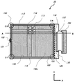
本実施形態1の液晶表示装置に用いられる液晶パネル10の構成について図1、図2、図3および図4の模式図を用いて説明する。図1は、液晶パネル全体の構成の平面図を示しており、図2は、図1におけるA−B断面線における断面図、図3および図4は、図1におけるコーナー部C1、C2での要部平面図をそれぞれ示したものである。尚、図は模式的なものであり、示された構成要素の正確な大きさなどを反映するものではない。また、図面が煩雑とならないよう、発明の主要部以外の省略や構成の一部簡略化などを適宜行っている。以下の図においても同様とする。更に、以下の図においては、図中、既出の図において説明したものと同一の構成要素には同一の符号を付し、適宜その説明を省略する。
Embodiment 1 FIG.
The configuration of the
ここでは、一例としてTFT(Thin Film Transistor)方式の2画面ディスプレイ液晶パネルについて説明を行うことにする。この液晶パネル10は、図に示される様に、スイッチング素子としてTFTがアレイ状に配置されるスイッチング素子基板(以下、TFT基板110)と、カラーフィルタなどの形成されるカラーフィルタ基板(以下、CF基板120)と、液晶パネル10が動作した際に画像を表示する表示面に対応する領域である表示領域100に対して、TFT基板110とCF基板120との間における、少なくとも表示領域100を囲うように配置された額縁領域101において設けられ、CF基板120とTFT基板110との間の間隙を密封するシールパターン130を備えている。
Here, as an example, a TFT (Thin Film Transistor) type two-screen display liquid crystal panel will be described. As shown in the figure, the
更にTFT基板110とCF基板120間には、基板間に所定の一定範囲の間隙を形成し保持する柱状スペーサ133、言い換えると、基板間の距離を一定範囲に保持する柱状スペーサ133が表示領域100内に多数配置される。柱状スペーサ133は、表示領域100内において、2種類設けられ、通常時において、TFT基板110とCF基板120間を所定の一定範囲の間隙に保持するメイン柱状スペーサ(以下、柱状スペーサ(メイン))133mと、柱状スペーサ(メイン)133mよりは低い高さに形成され、TFT基板110表面或いはCF基板120表面に押圧が掛かった場合など、TFT基板110とCF基板120間の間隔が通常時より狭まった際にTFT基板110表面或いはCF基板120表面に当接することにより、柱状スペーサ(メイン)133mと協働してTFT基板110とCF基板120間の間隔を一定範囲に保持する役割をするサブ柱状スペーサ(以下、柱状スペーサ(サブ))133sとが設けられる。
Further, between the
また、基板間の距離を一定範囲に保持する柱状スペーサ133は、額縁領域101においても設けられ、周辺柱状スペーサ(以下、柱状スペーサ(周辺))133dと呼ぶ。なお、柱状スペーサ(周辺)133dについては、柱状スペーサ(メイン)133mと同じ高さとして、通常時において、TFT基板110とCF基板120間を所定の一定範囲の間隙に保持するようにしても構わないが、ここでは、柱状スペーサ(サブ)133sと同様に柱状スペーサ(メイン)133mよりは低い高さに形成し、TFT基板110表面或いはCF基板120表面に押圧が掛かった際にのみ保持させる構成とした。また、これら柱状スペーサ133の種類ごとの詳細な配置については、本発明の主要なポイントであるので、後に別途詳細に説明を行う。
The
このシールパターン130により密封され、柱状スペーサ133により保持されたCF基板120とTFT基板110との間の間隙の少なくとも表示領域100に対応する領域に液晶材料が狭持されることにより、液晶層140Lが配置されている。また、シールパターン130には、液晶材料を注入するための開口部である注入口131が設けられ、この注入口131は、封止材132により封止されている。言い換えると、液晶材料は、シールパターン130により囲まれる領域に封止されている。ここでは、液晶材料として一般的なTN(Twisted Nematic)タイプの液晶材料を用いている。なお、ここで使用した表示領域100および額縁領域101については、液晶パネル10のTFT基板110上、CF基板120上、或いは両基板間に挟まれる領域の全てにおいて使用することとし、本明細書中においては全て同様の意味にて使用する。
The liquid crystal material is nipped in at least a region corresponding to the
上述のTFT基板110は、透明基板である厚み0.7mm程度の一般的なガラスよりなるガラス基板111の一方の面に液晶を配向させる配向膜112、配向膜112の下部に設けられ液晶を駆動する電圧を印加する画素電極113、画素電極113に電圧を供給するスイッチング素子であるTFT114、TFT114を覆う絶縁膜115、TFT114に信号を供給する配線である複数のゲート配線116およびソース配線117、TFT114に供給される信号を外部から受け入れる信号端子118、信号端子118から入力された信号を対向電極123へ伝達するためのトランスファ電極(図示省略)などを有している。また、ガラス基板111の他方の面には偏光板134を有している。
The
一方、上述のCF基板120は、透明基板である厚み0.1mm程度の極薄ガラスよりなるガラス基板121の一方の面に液晶を配向させる配向膜122、配向膜122の下部に配置され、TFT基板110上の画素電極113との間に電界を生じ液晶を駆動する共通電極123、共通電極123下部に設けられるカラーフィルタ124およびカラーフィルタ124間を遮光するため、或いは表示領域100に対応する領域外側に配置される額縁領域を遮光するために設けられる遮光層であるブラックマトリクス(Black Matrix:BM)125などを有している。また、ガラス基板121の他方の面には、2画面ディスプレイとして、視野方向を2方向に分離する遮光層である視差バリア126が配置されており、この視差バリア126においては、画素内に配置されるBM125の開口部とずれた位置にスリット状の開口部が形成され、視野方向を分離し制限している。更に、視差バリア126よりも外側には、偏光板135を有している。
On the other hand, the above-described
カラーフィルタ124としては、樹脂中に顔料などを分散させた色材層が選択でき、赤、緑、青などの特定の波長範囲の光を選択的に透過するフィルタとして機能し、これら異なる色の色材層が規則的に配列して構成される(詳細図である図3および図4では、それぞれ、カラーフィルタ124R、124G、124Bとして図示)。BM125は、カラーフィルタ124間以外に表示領域100外側の額縁領域にも配置され、CF基板120における額縁領域のほぼ全域に渡り形成されており、表示に不要な額縁領域におけるCF基板120中の光の透過を遮光している。BM125および視差バリア126を構成する遮光層としては、クロムと酸化クロムの積層膜などを用いた金属系の材料や樹脂中に黒色粒子を分散させた樹脂系の材料などを選択することができる。なお、配向膜より下層に、カラーフィルタ124とBM125を覆うように透明樹脂膜よりなるオーバーコート層を設ける構成としても構わない。
As the
また、TFT110基板とCF基板120はシールパターン130を介して貼り合わされており、表示領域100に配置される柱状スペーサ133により所定の基板間隔に保持されている。更にトランスファ電極と共通電極123は、トランスファ材により電気的に接続されており、信号端子118から入力された信号が共通電極123に伝達される。トランスファ材については、シールパターン130中に導電性の粒子などを混合することにより代用でき省略することも可能であり、本実施の形態では、導電性の粒子などを混合したシールパターン130を用い、図2からも解かるとおりシールパターン130と共通電極123は接触することから、トランスファ電極をシールパターン130に平面的に重なるように配置し、シールパターン130と接触して設けることにより、トランスファ電極と共通電極123についてシールパターン130を介して電気的に接続した。
Further, the
この他に、液晶パネル10は駆動信号を発生する制御基板136、制御基板136を信号端子118に電気的に接続するFFC(Flexible Flat Cable)137、光源となるバックライトユニット(通常は、表示面となるCF基板120側とは反対側であるTFT基板110の外側に対向して配置されるが、ここでは図示せず)などを備えており、これら部材と共に表示面となる表示領域100におけるCF基板120の外側の部分が開放された筐体(図示せず)の中に収納され、本実施の形態1の液晶表示装置を構成する。
In addition, the
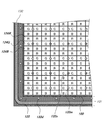
続いて、本実施の形態1の液晶パネル10の特徴部分である基板間の距離を一定範囲に保持する柱状スペーサ133の構成、更に、この柱状スペーサ133のパネル周辺部となるコーナー部での構成について、補足説明を行う。本実施の形態1の液晶パネル10では、図1中に示されるコーナー部C1〜C4において、特に液晶パネル10或いはCF基板120において注入口131が設けられる辺の両端に位置するコーナー部C1、C3と、この注入口131が設けられる辺と対向する辺の両端に位置するコーナー部C2、C4において、柱状スペーサ133の構成が異なっている。従って、柱状スペーサ133の構成が互いに異なるコーナー部C1とコーナー部C2を例に取って、図3および図4の平面図を用いて比較しながら説明を行う。図3はコーナー部C1での平面図、図4はコーナー部C2での平面図に相当する。
Subsequently, the configuration of the
先ず、コーナー部C1での柱状スペーサ133の構成について、図3を用い説明する。図3に示されるとおり、液晶パネル10或いはCF基板120において注入口131が設けられる辺の両端に位置するコーナー部C1においては、柱状スペーサ133について、表示領域100内においては、先にも説明したおり、柱状スペーサ(メイン)133mと柱状スペーサ(メイン)133mよりは低い高さに形成される柱状スペーサ(サブ)133sが設けられる。より具体的には、柱状スペーサ(メイン)133mと柱状スペーサ(サブ)133sが、緑の画素(124G)間の位置において、配置される位置と配置されない位置が交互に繰り返されている。更に行方向に配列する緑の画素列において、柱状スペーサ(メイン)133mが配置される緑の画素列と、柱状スペーサ(サブ)133sが配置される緑の画素列が交互に繰り返されている。つまり、柱状スペーサ(メイン)133mの配置密度と柱状スペーサ(サブ)133sの配置密度は等しく、柱状スペーサ(メイン)133mは、12個の画素に対して1個の割合、柱状スペーサ(サブ)133sについても12個の画素に対して1個の割合で設けられていることになる。
First, the structure of the
また、柱状スペーサ(サブ)133sを柱状スペーサ(メイン)133mよりも低くする程度としては、柱状スペーサ(メイン)133mの高さの15%程度、柱状スペーサ(サブ)133sの高さを低く設定した。つまり、柱状スペーサ(サブ)133sの高さは、柱状スペーサ(メイン)133mの高さの85%程度に設定されることとなる。 The column spacer (sub) 133s is set to be lower than the column spacer (main) 133m by about 15% of the height of the column spacer (main) 133m, and the column spacer (sub) 133s is set low. . That is, the height of the columnar spacer (sub) 133s is set to about 85% of the height of the columnar spacer (main) 133m.
また、この柱状スペーサ(メイン)133mと柱状スペーサ(サブ)133sの配置の割合は、コーナー部C1の近傍、コーナー部C1と同様に注入口131が設けられる辺の両端に位置するコーナー部C3においても共通しており、更に注入口131が設けられる辺と対向する辺の両端に位置するコーナー部C2、C4の近傍を除いて、表示領域100内において共通する配置割合としても良い。
Further, the arrangement ratio of the columnar spacer (main) 133m and the columnar spacer (sub) 133s is in the corner portion C3 located in the vicinity of the corner portion C1 and at both ends of the side where the
続いて、コーナー部C1と異なる配置を有するコーナー部C2での柱状スペーサ133の構成について、図4を用い説明する。このコーナー部C2における平面図である図4に示されるとおり、コーナー部C1の近傍での柱状スペーサ133の配置に比べて、コーナー部C2の近傍での柱状スペーサ133の配置は、高密度に配置されていることが解かる。より具体的には、柱状スペーサ(メイン)133mと柱状スペーサ(サブ)133sが、図3における配置とは違って、緑の画素(124G)間の位置における交互の位置ではなく、全ての位置において配置される。つまり、緑の画素(124G)間の位置の全ての位置において、柱状スペーサ(メイン)133mと柱状スペーサ(サブ)133sの何れかが配置されている。なお、行方向に配列する緑の画素列において、柱状スペーサ(メイン)133mが配置される緑の画素列と、柱状スペーサ(サブ)133sが配置される緑の画素列が交互に繰り返されている点は図3における配置と同じであることから、柱状スペーサ(メイン)133mの配置密度と柱状スペーサ(サブ)133sの配置密度は等しい。また、配置密度は、柱状スペーサ(メイン)133mは、6個の画素に対して1個の割合、柱状スペーサ(サブ)133sについても6個の画素に対して1個の割合で設けられ、図3における配置と比べると2倍の密度で配置されていることになる。
Next, the configuration of the
また、額縁領域101においても設けられる柱状スペーサ(周辺)133dについても、図3のコーナー部C1の配置密度に比べて、図4のコーナー部C2の配置密度は高い密度で配置されており、図示されるとおり、概ね2倍程度の密度で配置されている。なお、図3および図4に示される柱状スペーサ(周辺)133dについては、額縁領域101に対して、1列に配列して設けられた例を図示しているが、図が煩雑となることから最も簡略な例を示したものであり、額縁領域101の幅に応じて、適宜、複数列に配置すると良く、必ずしも配列する必要は無く定密度に分散して配置しても構わない。このように柱状スペーサ(周辺)133dを額縁領域101において複数列や定密度に分散して設ける場合にも、配置密度についてコーナー部C1の配置密度に比べて、コーナー部C2の配置密度が高い密度で配置されていれば良い。
Also, the columnar spacer (periphery) 133d provided also in the
以上のとおり構成について説明を行った本実施の形態1の液晶表示装置および液晶パネル10は次の様に動作する。例えば、制御基板136から電気信号が入力されると、画素電極113および共通電極123に駆動電圧が加わり、駆動電圧に合わせて液晶層140Lにおける液晶分子の方向が変わる。そして、バックライトユニットの発する光がTFT基板110、液晶層140LおよびCF基板120を介して観察者側に透過或いは遮断されることにより、液晶パネル10の表示領域100に映像などが表示される。
The liquid crystal display device and
なお、本実施の形態1の液晶表示装置は2画面ディスプレイ液晶パネルであることから、視差バリア126により、CF基板120を介して透過される光が2方向の所定の角度方向の視角範囲に制限される。具体的には表示面に対して、図2中の+X方向と−X方向の2方向に視角範囲を有して映像などが表示される。また、2方向の視角範囲に対応した表示画素が設定されて、それぞれ異なる映像表示を行うことにより、2方向の視角範囲に対して、それぞれ、異なる映像を表示し、2画面ディスプレイ液晶パネルとして機能する。また、本実施の形態1の液晶表示装置は、上述のとおりコーナー部での柱状スペーサ133の構成において特徴的構成を有していることから、ギャップムラや配向異常による表示不良が発生することの多かった極薄ガラスを用いた2画面ディスプレイ液晶パネルであるにも関わらず、ギャップムラや配向異常による表示不良の見られない高い表示品位を有する2画面ディスプレイ液晶パネルを得ることができた。
Since the liquid crystal display device according to the first embodiment is a two-screen display liquid crystal panel, light transmitted through the
次に、本実施の形態1の液晶表示装置および液晶パネル10の製造方法について説明を行う。先ず、本実施の形態1の液晶パネル10の組み立て工程の概要について、図5に示すフローチャートに従い説明を行うことにする。
Next, a method for manufacturing the liquid crystal display device and the
先ず、基板準備工程において、互いに貼り合わされる前のTFT基板110を取り出すマザーTFT基板とCF基板120を取り出すマザーCF基板を準備する(S1)。マザーTFT基板10とマザーCF基板20については、CF基板120は最終的にガラスを薄型化加工して極薄ガラスに形成されるが、以降の工程の実施が容易となるように、途中までは、厚み0.5〜1.5mm程度のガラスにより構成されるマザーTFT基板とマザーCF基板により製造される。ここでは、マザーTFT基板とマザーCF基板の両者ともに厚み0.7mmのガラスにより構成される基板として準備される。
First, in the substrate preparation step, a mother TFT substrate for taking out the
マザーTFT基板とマザーCF基板の製造方法については一般的な方法を用いても良いため、簡単に説明する。先ず、マザーTFT基板については、公知の製造方法を利用して、ガラス基板111の一方の面に、成膜、フォトリソグラフィー法によるパターンニング、エッチング等のパターン形成工程を繰り返し用いてTFT114や画素電極113、ゲート配線116やソース配線117などの配線層、更に端子118、トランスファ電極を形成することにより製造される。また、マザーCF基板は、ガラス基板121の一方の面に、同様に、公知の製造方法を利用して、成膜からパターン形成工程を繰り返し用いて、カラーフィルタ124、ブラックマトリクス125、共通電極123、有機樹脂膜をパターニングして形成された柱状スペーサ133を形成することにより製造される。なお、本発明の特徴的な構成である柱状スペーサ133についても、配置密度などのパターン設計の変更のみで良く、形成方法自体は公知の方法で製造することができる。
Since a general method may be used as a method for manufacturing the mother TFT substrate and the mother CF substrate, it will be briefly described. First, with respect to the mother TFT substrate, the
続いて、基板洗浄工程において、以上説明のとおり準備されたマザーTFT基板を洗浄する(S2)。次に、配向膜材料塗布工程において、マザーTFT基板の一方の面に、配向膜材料を塗布形成する(S3)。この工程は、例えば、印刷法により有機膜からなる配向膜材料を塗布し、ホットプレートなどにより焼成処理し乾燥させる。その後、ラビング工程において配向膜材料にラビングを行い、配向膜材料表面を配向処理し配向膜112とする(S4)。 Subsequently, in the substrate cleaning step, the mother TFT substrate prepared as described above is cleaned (S2). Next, in the alignment film material application step, an alignment film material is applied and formed on one surface of the mother TFT substrate (S3). In this step, for example, an alignment film material made of an organic film is applied by a printing method, and is baked and dried by a hot plate or the like. Thereafter, the alignment film material is rubbed in a rubbing process, and the alignment film material surface is subjected to alignment treatment to form the alignment film 112 (S4).
また、S2〜S4と同様に、マザーCF基板についても、洗浄、配向膜材料の塗布、ラビングを行うことにより配向膜122を形成する。続いて、シール剤塗布工程において、スクリーン印刷装置により、シール剤を印刷ペーストとして、マザーTFT基板或いはマザーCF基板の一方の面にシール剤の塗布を行い、最終的に表示領域100を囲う形状のシールパターン130を形成する(S5)。
Similarly to S2 to S4, the
続いて、貼り合わせ工程において、マザーTFT基板およびマザーCF基板を貼り合わせてセル基板を形成する(S6)。続いて、シール剤硬化工程において、マザーTFT基板とマザーCF基板を貼り合わせた状態で、シールパターン130を構成するシール剤を完全に硬化させる(S7)。この工程は、例えば、シール剤の材質に合わせて熱を加えることや紫外線を照射することにより行われる。
Subsequently, in the bonding step, the mother TFT substrate and the mother CF substrate are bonded together to form a cell substrate (S6). Subsequently, in the sealant curing step, the sealant constituting the
続いて、液晶パネル10を湾曲可能とするためや本実施の形態の様に2画面ディスプレイ液晶パネルを形成するために、この貼り合わされた状態で少なくとも一方のマザーTFT基板およびマザーCF基板を構成するガラス基板を極薄ガラスに薄型化加工する薄型化研磨工程を実施する(S8)。具体的には、薬液や機械的研磨による薄型化処理が選択できるが、例えば、薬液による薄型化処理を用いる場合、マザーTFT基板およびマザーCF基板の両者を薄型化する際には、マザーTFT基板とマザーCF基板の周辺部に対し薬液が基板間に入ることを防止する周辺封止を実施したうえで、貼り合わされたマザーTFT基板とマザーCF基板全体を薬液中に浸漬して、マザーTFT基板とマザーCF基板の表面を削り薄型化する。また、TFT基板10とCF基板20の一方のみ、例えば、本実施の形態1の様にCF基板20のみを薄型化するのであれば、周辺封止に加えてマザーTFT基板表面にレジストなどで保護層を形成した状態で、マザーCF基板の表面のみを削り薄型化すると良い。
Subsequently, in order to make the
更に、この薄型化されたマザーCF基板側の表面に2画面ディスプレイ液晶パネルとして機能させる構成である遮光層からなる視差バリア126を形成する視差バリア形成工程を行う(S9)。具体的には、視差バリア126を構成する材料に応じて、クロムと酸化クロムの積層膜などを用いた金属系の材料を成膜し、視差バリア126として機能させるための所定の位置にスリット状の開口部を有した形状に、この視差バリア126を構成する材料に応じたパターニング加工を実施する。なお、この金属系の材料の成膜処理については、基板加熱を伴うスパッタリングにより行われる。
Further, a parallax barrier forming step of forming a
続いて、セル分断工程において、貼り合わせたマザーTFT基板およびマザーCF基板を分断し、多数の個別セルに分断する(S10)。この工程は、スクライブ工程において、ガラス基板の表面に切断の起点となるスクライブラインを形成した後、このスクライブラインの近傍に応力を印加することにより分断が行われ、多数の個別セルの状態となる。 Subsequently, in the cell dividing step, the bonded mother TFT substrate and mother CF substrate are divided into a large number of individual cells (S10). In this step, a scribe line is formed on the surface of the glass substrate in the scribe step, and then, by applying stress in the vicinity of the scribe line, division is performed, resulting in a state of a large number of individual cells. .
続いて、液晶注入工程において、個別セルの注入口から液晶を注入する(S11)。この工程は、例えば、真空状態とされた真空注入装置内において、個別セルの注入口を液晶材料に接触させた状態で、徐々に装置内を大気圧とすることで、液晶材料が注入口からセル内に注入、つまり、充填されることにより行われる。更に、注入口封止工程において、注入口を封止する(S12)。この工程は、例えば、注入口を光硬化型樹脂で封じ、光を照射することにより行われる。なお、この液晶注入工程(S11)が、本発明による作用が発揮される重要な工程となることから、別途、詳細に説明することにする。 Subsequently, in the liquid crystal injection step, liquid crystal is injected from the injection port of the individual cell (S11). This step is performed, for example, in a vacuum injecting apparatus that is in a vacuum state, with the inlet of the individual cell being in contact with the liquid crystal material, and gradually bringing the inside of the apparatus to atmospheric pressure, so that the liquid crystal material is removed from the injecting port. This is done by filling, ie filling, the cell. Further, in the inlet sealing step, the inlet is sealed (S12). This step is performed, for example, by sealing the injection port with a photocurable resin and irradiating with light. Since this liquid crystal injection step (S11) is an important step in which the effect of the present invention is exhibited, it will be separately described in detail.
この様に個々の液晶パネルの形状に分断され、液晶材料が充填され、封止された後、偏光板貼り付け工程において、セル基板の外側のTFT基板110およびCF基板120のそれぞれの表面に偏光板134および偏光板135を貼り付け(S13)、制御基板実装工程において、制御基板136を実装する(S14)ことによって、液晶パネル10が完成する。更に、液晶パネル10の反視認側となるTFT基板110の裏面側に位相差板などの光学フィルムを介して、バックライトユニットを配設し、樹脂や金属などよりなるフレーム内に、液晶パネル10およびこれら周辺部材を適宜収納し、本実施の形態1の液晶表示装置が完成する。
In this way, after being divided into individual liquid crystal panel shapes, filled with a liquid crystal material and sealed, in the polarizing plate attaching step, polarized light is applied to the respective surfaces of the
続いて、本発明の特徴的な工程である液晶注入工程(S11)について、図6〜図9の説明図を用いながら詳細に説明することにする。先ず、液晶注入工程(S11)における液晶材料140が個別セル20内へ引き込まれる際に発生する現象の概要について、図6を用い説明する。図6(a)は、液晶注入工程での真空注入装置220内において液晶材料140が個別セル20内に引き込まれる様子を示す概略図、図6(b)は、個別セル20の特に図6(a)でのコーナー部C2、C4での断面図をそれぞれ示したものである。図6(a)にて示されるとおり、個別セル20を真空注入装置220内に収納した状態で、真空ポンプPが動作されることで真空状態とされた真空注入装置220内において、個別セル20の注入口131を液晶皿210内に満たされた液晶材料140に接触させた状態で、徐々に装置内を大気圧とすることで、液晶材料140が注入口131から個別セル20内に引き込まれる。図6(a)は、個別セル20内の全体に液晶材料140が充填される少し前の段階での状態を示している。
Next, the liquid crystal injection process (S11), which is a characteristic process of the present invention, will be described in detail with reference to the explanatory diagrams of FIGS. First, an outline of a phenomenon that occurs when the
図6(a)に示すとおり、注入口131が設けられる辺と対向する辺の両端に位置するコーナー部C2、C4の近傍では、注入口131より最も距離の離れた位置に相当することから、未だ、液晶材料140の充填が完了していない状態、つまり、気泡141が形成されている状態である。また、このコーナー部C2、C4の近傍では、個別セル20内(気泡141内)は、ほぼ真空に近い状態となっている。一方、真空注入装置220内は、既にほぼ大気圧まで戻りつつあることとなる。従って、図6(b)の断面図で示されるとおり、セル外よりTFT基板110表面とCF基板120表面には大気圧相当の圧力Patが作用する状態となっており、逆に、この気泡141内では、未だ、ほぼ真空に近い状態であることから、この圧力Patが気泡141内に配置される柱状スペーサ133に直接的に作用することとなる。この様な状態は、真空注入方式で形成される液晶パネルにおいては共通して発生する状況であり、特別な状況では無い。
As shown in FIG. 6A, in the vicinity of the corner portions C2 and C4 located at both ends of the side opposite to the side where the
以上の状況を踏まえたうえで、続いて、図7、図8を用いて、本実施の形態1の液晶表示装置で液晶注入工程(S11)において発生する現象と作用について説明を行う。図7は、注入口131が設けられる辺と対向する辺の両端に位置するコーナー部C2における断面図を示したものであり、図7(a)は、液晶注入工程(S11)開始前の状態、図7(b)は、液晶注入工程の完了する少し前、丁度、先に説明した図6(a)と同じくらいの時点での状態、図7(c)は、完了時の状態をそれぞれ示したものである。図8は、注入口131が設けられる辺の両端に位置するコーナー部C1における断面図を示したものであり、図7と同様に、図8(a)は、液晶注入工程(S11)開始前の状態、図8(b)は、液晶注入工程の完了する少し前、丁度、図6(a)と同じくらいの時点での状態、図8(c)は、完了時に状態をそれぞれ示したものである。
Based on the above situation, the phenomenon and action that occur in the liquid crystal injection step (S11) in the liquid crystal display device of the first embodiment will be described below with reference to FIGS. FIG. 7 shows a cross-sectional view of the corner portion C2 located at both ends of the side opposite to the side where the
先ずは、液晶注入工程(S11)開始前の状態について、注入口131より離れた位置のコーナー部C2を示す図7(a)と、注入口131に近い位置のコーナー部C1を示す図8(a)を比較する。本実施の形態1の液晶表示装置および液晶パネル10の構成を説明する際に図3、図4を用い説明したとおり、図7(a)と図8(a)の比較でも、柱状スペーサ133の配置について、注入口131より離れた位置のコーナー部C2では、注入口131に近い位置のコーナー部C1の配置密度に比べて高い密度で配置されている。また、この段階では、特にTFT基板110とCF基板120(正確にはマザーTFT基板とマザーCF基板)間には、外部より圧力などが加わっておらず、TFT基板110とCF基板120間は、柱状スペーサ(メイン)133mがTFT基板110とCF基板120に当接することにより保持されている。
First, in a state before the liquid crystal injection step (S11) is started, FIG. 7A showing the corner portion C2 at a position away from the
続いて、液晶注入工程の完了する少し前の時点で、注入口131に近い位置のコーナー部C1では、図8(b)に示すとおり、液晶材料140は、シールパターン130近傍まで充填が完了している。一方、注入口131より離れた位置のコーナー部C2では、液晶材料140は、未だ、シールパターン130より遠く、額縁領域101にかかり始めた程度である。また、セルの外側では、既に大気圧近くまで戻っていることから、TFT基板110とCF基板120には、セルの外側より、概ね大気圧に相当する圧力Patが加わっている。この大気圧に対して、セルの内側からは、液晶材料140の圧力PLCと柱状スペーサ133が圧縮されて生ずる反発力が抗力(反力)として作用することとなる。液晶材料140の圧力PLCは、液晶皿210表面より作用する大気圧相当の圧力が伝達されていることから、セルの外側からの圧力に近い圧力となっている。
Subsequently, at a point just before the completion of the liquid crystal injection step, the
なお、セルの内側から働く反力として、一般的な液晶パネル、つまり、本実施の形態1で用いているような極薄ガラスを用いない場合には、シールパターン130で貼り合わされたTFT基板110とCF基板120により構成されるセル構造自体によって、セル構造を歪ませる変形力、特にここで問題となるTFT基板110とCF基板120間の距離を狭める方向に変形する力に対して、変形を妨げる反発力を生ずる。然しながら、本実施の形態1のように極薄ガラスを用いた場合には、極薄ガラスの強度の面で、この反発力が非常に弱くなる。従って、本実施の形態1の場合においては、先に説明のとおり、実質的には、セルの内側から働く反力としては、液晶材料140の圧力PLCと柱状スペーサ133による反発力のみを考慮すれば良い。
In addition, as a reaction force acting from the inside of the cell, when a general liquid crystal panel, that is, an ultrathin glass as used in the first embodiment is not used, the
注入口131に近い位置のコーナー部C1では、液晶材料140の充填が概ね完了していることから、図8(b)に示すとおり、柱状スペーサ133は、それ程、圧縮変形されることなく上記説明のバランスが保たれる。一方、注入口131より離れた位置のコーナー部C2では、この液晶材料140による圧力PLCは、殆ど充填されていない額縁領域101では反力として作用せず、セルの外側からの大気圧相当の圧力Patは、殆ど柱状スペーサ133の圧縮により生ずる反発力で保持されることとなる。従って、図7(b)に示すとおり、額縁領域101とその近傍では、設けられている全ての柱状スペーサ133(柱状スペーサ(メイン)133m、柱状スペーサ(サブ)133s、および柱状スペーサ(周辺)133d)がTFT基板110とCF基板120に当接され、更に圧縮変形されることで、バランスが保たれている。
Since the filling of the
ここで、図9は、比較例として、仮に注入口131より離れた位置のコーナー部C2でも、注入口131に近い位置のコーナー部C1と同じ程度の比較的低い密度で柱状スペーサ133を配置して液晶注入工程を行った場合について示すものであり、この比較的低い密度で柱状スペーサ133を配置した場合でのコーナー部C2について、本実施の形態1について説明した図7(a)〜図7(c)の状態に対応して示している。
Here, FIG. 9 shows a comparative example in which the
図7(b)を用い説明したおり、注入口131より離れた位置のコーナー部C2では、セルの外側からの大気圧相当の圧力Patは、殆ど柱状スペーサ133の圧縮により生ずる反発力で保持されることとなる。従って、額縁領域101とその近傍では、設けられている全ての柱状スペーサ133(柱状スペーサ(メイン)133m、柱状スペーサ(サブ)133s、柱状スペーサ(周辺)133d)がTFT基板110とCF基板120に当接され、圧縮変形されることで、バランスが保たれることとなる。然しながら、図9(b)に示すとおり、比較的低い密度で柱状スペーサ133を配置している場合には、この少ない柱状スペーサ133に対し、セルの外側より加わる概ね大気圧に相当する圧力Patが集中することから、本実施の形態1での図7(b)と比較して、柱状スペーサ133は大きく変形されることとなる。
As described with reference to FIG. 7B, in the corner portion C <b> 2 far from the
例えば、図9(b)では、それぞれの柱状スペーサ133の変形前の形状(高さ)を点線にて示しているが、特に柱状スペーサ(メイン)133mは元の高さの半分を大きく下回る程度まで、その他の柱状スペーサ133についても半分程度まで変形されている。仮にこれら柱状スペーサ133を構成する部材の弾性変形範囲が50%変形まで、更に変形に追従できずに破壊或いは損傷に至る範囲が60%変形までとすると、殆どの柱状スペーサ133は、弾性変形範囲に収まらず塑性変形を起こし、更に一部の変形量が大き過ぎるものは、破壊或いは損傷に至ることとなる(一部、破壊或いは損傷された状態を破損した柱状スペーサ133brとして図示)。一方、本実施の形態1での同じ状態を示す図7(b)では、柱状スペーサ133が比較的高い密度で配置されていることから、それぞれの柱状スペーサ133で加わる圧力が分散されることから、変形量は、50%変形よりも少ない程度、すなわち、弾性変形範囲内に納まっていることとなる。
For example, in FIG. 9B, the shape (height) before deformation of each
続いて、液晶注入工程の完了時では、図7(c)、図8(c)に示されるとおり、コーナー部C1、コーナー部C2の何れにおいても、セル内は、液晶材料140により満たされており、額縁領域101も含めて大気圧相当の圧力Patと液晶材料140の圧力PLCはバランスする。特に途中までは変形されていた柱状スペーサ133は、本実施の形態1では、何れも弾性変形の範囲内で変形されていたこととなることから、圧縮される圧力が除去(開放)されれば、概ね元の高さまで回復する。つまり、柱状スペーサ(メイン)133mによる保持で決定される所定のギャップとなる。なお、比較例の場合には、図9(c)に示すとおり、一旦、塑性変形を生じた柱状スペーサ133については、不可逆な変形であることから、額縁領域101も含めて液晶材料140の充填が完了して圧力が除去(開放)されたとしても元の高さには戻らない(塑性変形した柱状スペーサ133plとして図示)。また、一旦、破損した柱状スペーサ133brについても元に戻らないことは言うまでもない。従って、額縁領域101の近傍で適正に保持するスペーサが存在しなくなることから、所定のギャップよりは狭く、ギャップ不良を生じることとなる。このギャップ不良は、額縁領域101近傍の表示領域100まで及ぶことから、表示においてもムラなどを生ずることとなる。また、破損した柱状スペーサ133brは、仮に表示に直接寄与しない額縁領域101に設けられる柱状スペーサ133であっても、破損した柱状スペーサ133brより、構成する成分が不純物として液晶中に溶出し、液晶が汚染されることによる信頼性も低下してしまうことにつながる。
Subsequently, at the completion of the liquid crystal injection step, as shown in FIGS. 7C and 8C, the cell is filled with the
なお、上述の図7〜図9を用いた液晶注入工程についての詳細説明で用いた柱状スペーサ133の弾性変形範囲と破壊或いは破損に至る変形量については、用いる柱状スペーサ133を構成する樹脂の種類や形状、更に、その前に行われる視差バリア形成工程(S9)におけるスパッタリングによる遮光層の成膜工程などによる加熱処理条件、つまり樹脂の劣化(弾性変形範囲がより狭く、破壊や破損に至る変形量がより小さくなる)の程度によって変動することとなる。また、例示した変形量は、図示での都合、説明の便宜上用いた値であり、実際の変形量、特に、視差バリア形成工程での加熱処理を経ることとなる極薄ガラス基板表面に直接形成された視差バリアを備えた液晶表示装置の場合での変形量については、例示した変形量よりは、かなり小さい変形量で、塑性変形の発生や破壊などが発生することとなる。
The elastic deformation range of the
以上、説明を行ったとおり、本実施の形態1の液晶表示装置においては、注入口131に近い位置のコーナー部C1に比べ、注入口131より離れた(遠い)位置のコーナー部C2で液晶注入時において基板間の間隔を一定範囲に保持するスペーサ構造として機能する構成である柱状スペーサ133の配置密度を高くしていることで、極薄ガラスが用いられている液晶表示装置を真空注入方式による液晶注入方法を用い製造した場合において、注入口131より離れたコーナー部で柱状スペーサ133が塑性変形や破壊或いは損傷されることを防止することができる。その結果、2画面ディスプレイの製造において、特に遮光層の設計に制約事項が設けられることのない真空注入方式による液晶注入方法を選択することができると共に、上記説明の注入口131より離れたコーナー部で柱状スペーサ133が塑性変形や破壊或いは損傷されることが無いことから、当該コーナー部でギャップムラや配向異常による表示不良が発生することが無い。更に、柱状スペーサ133の破壊或いは損傷が生じないことから、柱状スペーサ133を構成する成分が不純物として液晶中に溶出し、液晶が汚染されることによって信頼性が低下することも無い。以上のことから、良好な歩留まりで低コストにて製造することが可能であり、高い信頼性と良好な表示品位を有する2画面ディスプレイを得ることができる。
As described above, in the liquid crystal display device according to the first embodiment, the liquid crystal injection is performed at the corner portion C2 at a position (distant) from the
また、注入口131に近い位置のコーナー部C1に比べ、注入口131より離れた位置のコーナー部C2で柱状スペーサ133の配置密度を高くすることで、上記説明の本発明の基本的な効果については得ることができるが、より適正とするためには、コーナー部C2での柱状スペーサ133の配置密度について、柱状スペーサ133に対して、最大限の負荷となる大気圧が負荷された際における当該柱状スペーサ133の変形量が上記説明の柱状スペーサ133の弾性変形範囲内に納まる程度に分散されるように柱状スペーサ133の配置密度を調整すると良い。なお、ここで言う柱状スペーサ133の変形量が弾性変形範囲内に納まるというのは、配置される幾つかの柱状スペーサ133で、それぞれ変形量が異なる場合もあるが、全ての柱状スペーサ133について不具合を生じないことが望まれることから、全ての柱状スペーサ133について弾性変形範囲内に納まることに相当し、少なくとも最も大きく変形されるものが弾性変形範囲内に納まれば良いことにも相当する。また、ここでの調整に用いる柱状スペーサ133の弾性変形範囲に関する特性は、液晶注入工程直前での特性、つまり、液晶注入工程までに柱状スペーサ133が経た熱履歴による劣化後の特性を元にすると良い。
Further, by increasing the arrangement density of the
また、適当な配置密度(単位面積あたりの個数)については、一つの柱状スペーサ133の断面積により変わることから、ここで意味する配置密度は、実質的には面積密度と解釈した方が良い。つまり、注入口131に近い位置のコーナー部C1に比べ、注入口131より離れた位置のコーナー部C2で柱状スペーサ133の配置密度について、面積密度において高くすることにより、本発明の効果が得られると言い換えられる。
Further, since the appropriate arrangement density (number per unit area) varies depending on the cross-sectional area of one
続いて、実施の形態1からの一つの変形例について、図10および図11(実施の形態1における図3および図4に対応する位置について、それぞれ、図10および図11で示している)を用い説明を行う。本発明に従って、注入口131より離れた位置のコーナー部C2で柱状スペーサ133の配置密度を高くするにあたり、一般的な柱状スペーサにより基板を保持する液晶パネルにおいて、絶えずTFT基板とCF基板の両者に当接して保持することとなる柱状スペーサ(メイン)について、あまり密度を増加してしまうと、液晶パネルが低温に曝された際に気泡が発生する現象(低温発泡と呼ばれる)や、高温に曝された際に、立てて動作された液晶パネルの下側領域でギャップが広く膨れ表示ムラの発生する現象(下膨れ現象或いは重力ムラ現象と呼ばれる)などが生じ易くなることを考慮する必要がある。
Subsequently, FIG. 10 and FIG. 11 (the positions corresponding to FIG. 3 and FIG. 4 in the first embodiment are shown in FIG. 10 and FIG. 11 respectively) for one modification from the first embodiment. Use explanation is given. According to the present invention, in increasing the arrangement density of the
一方、本発明においては、TFT基板110とCF基板120表面に対し大気圧がかかり、ある程度、基板間が狭くなった際に、TFT基板110とCF基板120間ギャップを保持、つまり、圧力を分散して保持できれば良いことから、絶えずTFT基板110とCF基板120の両者に当接して保持することとなる柱状スペーサ(メイン)133mに限られず、液晶注入時に基板間が狭くなった際において、基板間の間隔を一定範囲に保持するスペーサ構造として有効に機能する構成である柱状スペーサ(メイン)133m、柱状スペーサ(サブ)133s、柱状スペーサ(周辺)133dの何れの構成でも良く、これら何れかの構成の柱状スペーサ133で配置密度を高くできれば良い。従って、この変形例では、図10および図11に示すように、コーナー部C2について、額縁領域101では、実施の形態1と同様に柱状スペーサ(周辺)133dの密度を増加し、表示領域100では、柱状スペーサ(メイン)133mの密度は、コーナー部C1或いは表示領域100全体で同じ密度で配置し、柱状スペーサ(サブ)133sについてのみ密度を増加している。
On the other hand, in the present invention, when the atmospheric pressure is applied to the surfaces of the
このように、注入口131より離れた位置のコーナー部C2で柱状スペーサ133の配置密度を高くするにあたり、絶えずTFT基板110とCF基板120の両者に当接して保持することとなる柱状スペーサ(メイン)133mについては、コーナー部C2とコーナー部C1において密度を変えることなく、柱状スペーサ(メイン)133mよりも低く形成されること、或いは、通常時はTFT基板110とCF基板120の一方のみに当接し、TFT基板110とCF基板120間が柱状スペーサ(メイン)が弾性変形する範囲で近接された際にのみTFT基板110とCF基板120の両者に当接して基板間ギャップを保持する柱状スペーサについて、コーナー部C1に比較してコーナー部C2において配置密度を高くすること、具体的には、柱状スペーサ(サブ)133s或いは柱状スペーサ(周辺)133dについて、コーナー部C2において配置密度を高くすることによって、上記説明のとおり、絶えずTFT基板110とCF基板120に当接して保持することとなる柱状スペーサ(メイン)133mの密度を増加することにより発生する低温発泡や下膨れなどの不具合を増加することなく、本発明の基本的な効果を得ることができる。
As described above, in increasing the arrangement density of the
注入口131より離れた位置のコーナー部C2で柱状スペーサ133の配置密度(面積密度)を高くするにあたり、実施の形態1のように、注入口131に近い位置のコーナー部C1にも配置される柱状スペーサ(メイン)133m、柱状スペーサ(サブ)133s、および柱状スペーサ(周辺)133dの何れかのスペーサ構造の範囲内のみで配置密度(面積密度)を調整する必要は無い。基板間の間隔を一定範囲に保持するスペーサ構造であれば、コーナー部C2に、適宜、柱状スペーサ(メイン)133m、柱状スペーサ(サブ)133s、および柱状スペーサ(周辺)133dとは異なる形状や形態を有した特別なスペーサ構造を追加しても良く、その場合にも、実施の形態1と同様の効果が得られる。続いて、図12および図13を用いて、コーナー部C2に、実施の形態1とは異なる形状や形態を有した基板間を保持するスペーサ構造を追加した幾つかの変形例について、順に説明を行う。
In order to increase the arrangement density (area density) of the
先ず、コーナー部C2で柱状スペーサ133の配置密度(面積密度)を高くするために追加される基板間を保持するスペーサ構造として、図12に示すとおり、コーナー部C2の近傍の特に額縁領域101に、ある程度の長さに延在して形成される土手状のスペーサ133aを設けても良い。特に、この様な土手状のスペーサ133aは、単純に面積密度を増加する作用に加えて、強度的にも優れていることから、その他の柱状スペーサ133などに加わる圧力を分散する効果が高い。但し、液晶が充填される際に、相対的に遅くなるコーナー部C2へ向かう方向への液晶の流れを妨げてしまっては、コーナー部C2での液晶の充填が遅れ、広い領域で液晶が充填されないまま外部が大気圧となってしまう。つまり、圧力を分散する必要のある領域が広くなり、基板間を保持するスペーサ構造を追加した効果が弱まってしまう。従って、図12に示すとおり、土手状のスペーサ133aは、コーナー部で分割されて、コーナー部方向(コーナー部へ向かう対角方向)で開口部が形成されていることが望ましい。この様なパターン構造とすることにより、開口部よりコーナー部方向へ液晶が流れ、コーナー部C2へ向かう方向への液晶の流れが妨げられることを最小限とすることができる。なお、土手状のスペーサ133aの高さについては、実施の形態1において、額縁領域101に設けた柱状スペーサ(サブ)133sと同様に、柱状スペーサ(メイン)133mよりも低い高さとして、やはり、コーナー部C2へ向かう方向への液晶の流れを、より妨げない構成とすることが望ましい。
First, as shown in FIG. 12, in the
同様の観点から、コーナー部C2で柱状スペーサ133の配置密度(面積密度)を高くするために追加される基板間を保持するスペーサ構造として、図13(a)に示す変形例のとおり、コーナー部C2の近傍の特に額縁領域101に設ける土手状のスペーサ133bについては、コーナー対角方向に沿って長手方向を揃えて配列して設けても良い。この構成については、図12に示す構成と比較して、コーナー部C2へ向かう方向への液晶の流れを妨げない作用に優れ、迅速にコーナー部C2への液晶の充填が進むとともに、コーナー部C2において配列した構造であることによって、補強効果にも優れている。このコーナー対角方向に沿って、配列して設けられる土手状のスペーサ133bについても、図12に示す構成と同様に柱状スペーサ(メイン)133mよりも低い高さとして、コーナー部C2へ向かう方向への液晶の流れを、より妨げない構成とすることが望ましい。
From the same point of view, as a spacer structure for holding between the substrates added in order to increase the arrangement density (area density) of the
更なる変形例としては、図13(b)に示す変形例のとおり、コーナー部C2で柱状スペーサ133の配置密度(面積密度)を高くするために追加される基板間を保持するスペーサ構造として、コーナー部C2において円形(円柱形状)の柱状スペーサ(周辺)133eを密集して配置しても良く、この構成の場合にも、コーナー部C2へ向かう方向への液晶の流れを妨げない作用に優れ、迅速にコーナー部C2への液晶の充填が進むとともに、コーナー部C2において、ある程度密集して配置されることから、補強効果にも優れている。また、このコーナー部C2において密集して配置される円形の柱状スペーサ(周辺)133eについても、図12に示す構成と同様に柱状スペーサ(メイン)133mよりも低い高さとして、コーナー部C2へ向かう方向への液晶の流れを、より妨げない構成とすることが望ましい。
As a further modified example, as a modified example shown in FIG. 13B, as a spacer structure for holding between the substrates added to increase the arrangement density (area density) of the
なお、実施の形態1および変形例において、基板間を保持するスペーサ構造として、柱状スペーサ(メイン)133mと共に配置密度(面積密度)を調整する柱状スペーサ(サブ)133s、柱状スペーサ(周辺)133d、土手状のスペーサ133a、土手状のスペーサ133b、および円形の柱状スペーサ(周辺)133eについて、柱状スペーサ(メイン)133mよりも低い高さに設定する場合、実施の形態1における柱状スペーサ(サブ)133sについては、柱状スペーサ(メイン)133mの高さの85%程度の高さに柱状スペーサ(サブ)133sの高さを設定した。つまり、柱状スペーサ(メイン)133mの高さが15%圧縮された時点で、柱状スペーサ(メイン)133mと柱状スペーサ(サブ)133sは、ほぼ同じ高さとなり、更なる圧縮方向の圧力が作用する場合には、柱状スペーサ(メイン)133mと柱状スペーサ(サブ)133sのそれぞれで加わる圧力が分散されることとなる。その他の柱状スペーサ(周辺)133d、土手状のスペーサ133a、土手状のスペーサ133b、および円形の柱状スペーサ(周辺)133eについて低くする程度は、具体的に述べなかったが、柱状スペーサ(メイン)133mの圧縮に対する弾性変形範囲内に収まることが、前提であることから、柱状スペーサ(サブ)133sで設定した高さと同等に設定すれば問題は無い。
In the first embodiment and the modification, as spacer structures for holding the gap between the substrates, columnar spacers (sub) 133s, columnar spacers (periphery) 133d, which adjust the arrangement density (area density) together with columnar spacers (main) 133m, When the bank-shaped spacer 133a, the bank-shaped
また、これら柱状スペーサ(メイン)133mと共に配置密度(面積密度)を調整する柱状スペーサ(サブ)133s、柱状スペーサ(周辺)133d、土手状のスペーサ133a、土手状のスペーサ133b、および円形の柱状スペーサ133eについて、液晶注入時において基板間を保持するスペーサ構造として、特に不具合を生じずに有効に作用させるために許容される高さ(低く形成して良い程度)としては、柱状スペーサ(メイン)133mとの高さの差が、少なくとも柱状スペーサ(メイン)133mの圧縮に対する弾性変形範囲内に収まれば、柱状スペーサ(メイン)133mが塑性変形や破壊に至る前には、これら基板間を保持するスペーサ構造として加わる圧力が分散され、柱状スペーサ(メイン)133mにかかる圧力を緩和することができる。つまり、柱状スペーサ(サブ)133s、柱状スペーサ(周辺)133d、土手状のスペーサ133a、土手状のスペーサ133b、および円形の柱状スペーサ133eが、柱状スペーサ(メイン)133mと同様に、液晶注入時において基板間を保持するスペーサ構造として不具合を生じすることなく有効に機能し、配置密度(面積密度)を調整することにより、本発明の効果を発揮することとなる。
In addition, the columnar spacer (sub) 133s, the columnar spacer (periphery) 133d, the bank-shaped spacer 133a, the bank-shaped
従って、液晶注入時において基板間を保持するスペーサ構造として有効に機能するかは、柱状スペーサ(メイン)133mの弾性変形範囲の大小に応じて決まることとなり、例えば、弾性変形範囲が比較的大きければ、より低い柱状スペーサ(サブ)133s、柱状スペーサ(周辺)133d、土手状のスペーサ133a、土手状のスペーサ133b、および円形の柱状スペーサ133eを採用しても良いこととなる。なお、柱状スペーサ(メイン)133mが、一般的な感光性樹脂により構成される場合には、実施の形態1の柱状スペーサ(サブ)133sで設定した程度で支障は無い。
Therefore, whether or not it effectively functions as a spacer structure for holding the gap between the substrates at the time of liquid crystal injection depends on the size of the elastic deformation range of the columnar spacer (main) 133m. For example, if the elastic deformation range is relatively large The lower columnar spacer (sub) 133s, the columnar spacer (periphery) 133d, the bank-shaped spacer 133a, the bank-shaped
また、実施の形態1および変形例におけるこれら柱状スペーサ(メイン)133m、柱状スペーサ(サブ)133s、柱状スペーサ(周辺)133d、土手状のスペーサ133a、土手状のスペーサ133b、および円形の柱状スペーサ133eについては、何れも基板間の間隔を所定の一定範囲に保持するスペーサ構造として機能するが、この所定の一定範囲としては、基板間の間隔の上限としては、柱状スペーサ(メイン)133mが元の高さ、つまり、変形されない高さに相当する。一方、基板間の間隔の下限としては、液晶注入時に、それぞれの位置において基板間が最も狭くなった際におけるスペーサ構造の高さに相当すると解釈して良い。また、柱状スペーサ(メイン)133mより低く形成され、液晶注入時において、TFT基板110とCF基板120間が近接された際にのみTFT基板110とCF基板120の両者に当接して基板間ギャップを保持するスペーサ構造については、上記の所定の一定範囲の下限を決定することのみに寄与することとなる。また、これら柱状スペーサ(メイン)133m、柱状スペーサ(サブ)133s、柱状スペーサ(周辺)133d、土手状のスペーサ133a、土手状のスペーサ133b、および円形の柱状スペーサ133eなどの基板間の間隔を所定の一定範囲に保持するスペーサ構造により基板間の間隔が所定の一定範囲における下限に保持される際に全てのスペーサ構造について弾性変形範囲内に納まるよう設定されることが望ましいことになり、これらスペーサ構造の配置密度などを調整すると良い。
Further, the columnar spacer (main) 133m, the columnar spacer (sub) 133s, the columnar spacer (periphery) 133d, the bank-shaped spacer 133a, the bank-shaped
なお、実施の形態1および変形例では、柱状スペーサ(メイン)133mも柱状スペーサ(サブ)133sも、それぞれ一体の構成とされているが、例えば、柱状スペーサ(メイン)133mは、CF基板120に設けられた円柱形状の樹脂パターンと、TFT基板110に設けられた金属膜パターンとが、当接して構成されること、つまり、2種の部材により構成され、柱状スペーサ(サブ)133sは、柱状スペーサ(メイン)133mを構成する円柱形状の樹脂パターンのみにより構成されることで、高さが低く形成されていても良い。つまり、この様な形態の場合には、金属膜パターンの有無の差だけ、つまり、金属膜パターンの厚み分だけ、柱状スペーサ(サブ)133sは、柱状スペーサ(メイン)133mに比べて低く形成されることとなる。
In the first embodiment and the modification, the columnar spacer (main) 133m and the columnar spacer (sub) 133s are integrated with each other. For example, the columnar spacer (main) 133m is formed on the
なお、実施の形態1および変形例では、一方の基板のみが極薄ガラスとなる2画面ディスプレイ液晶パネルへの本発明の適用例について説明を行った。本発明は、少なくとも一方の基板が極薄ガラスにより構成される場合に共通の効果が得られることから、TFT基板とCF基板の双方に極薄ガラスが使用される湾曲ディスプレイや、一方の基板に極薄ガラスが用いられる反射型ディスプレイなどへの適用が可能である。 In the first embodiment and the modification, the application example of the present invention to the two-screen display liquid crystal panel in which only one substrate is made of ultrathin glass has been described. In the present invention, a common effect is obtained when at least one of the substrates is made of ultrathin glass. Therefore, a curved display in which ultrathin glass is used for both the TFT substrate and the CF substrate, The present invention can be applied to a reflection type display using ultra-thin glass.
また、極薄ガラスとみなす基板厚さの範囲としては、実施の形態1および変形例では、0.1mm程度を代表的な厚さとして説明を行ったが、0.2mm未満程度において、実施の形態1および変形例において説明を行った効果について、一般的な液晶表示装置で用いられる程度の薄板ガラスである基板厚さ0.3mm程度のガラス基板を用いた液晶表示装置に比べて有意の効果が得られる。また、下限については、先行文献にも記載のある液晶表示装置で用いられるガラス基板の下限の基板厚さである0.01mm以上の範囲と解釈する。従って、本明細書で用いる極薄ガラスは、0.01mm以上、0.2mm未満の範囲の基板厚さを有するガラスであると定義し、この意味にて記載するものとする。以上のことから、本発明の効果としては、実施の形態1および変形例において例示した0.1mm程度の極薄ガラスに限られず、0.01mm以上、0.2mm未満の範囲の基板厚さを有する極薄ガラスを用いた場合にも実施の形態1および変形例と同様の効果を得ることができる。 In addition, as the range of the substrate thickness regarded as the ultrathin glass, in the first embodiment and the modification, the description has been made with a typical thickness of about 0.1 mm. About the effect demonstrated in the form 1 and the modification, it is a significant effect compared with the liquid crystal display device using the glass substrate about 0.3 mm of board | substrate thickness which is a thin glass about the grade used for a general liquid crystal display device. Is obtained. The lower limit is interpreted as a range of 0.01 mm or more which is the lower limit substrate thickness of the glass substrate used in the liquid crystal display device described in the prior literature. Therefore, the ultrathin glass used in this specification is defined as glass having a substrate thickness in the range of 0.01 mm or more and less than 0.2 mm, and is described in this sense. From the above, the effect of the present invention is not limited to the ultrathin glass of about 0.1 mm exemplified in the first embodiment and the modification, and the substrate thickness is in the range of 0.01 mm or more and less than 0.2 mm. Even when the ultra-thin glass is used, the same effects as those of the first embodiment and the modification can be obtained.
10 液晶パネル、100 表示領域、101 額縁領域、
110 TFT基板、120 CF基板、111,121 ガラス基板、
112,122 配向膜、113 画素電極、114 TFT、115 絶縁膜、
116 ゲート配線、117 ソース配線、118 信号端子、
123 共通電極、124 カラーフィルタ、125 BM、126 視差バリア、
130 シールパターン、131 注入口、132 封止材、
133 柱状スペーサ、133m メイン柱状スペーサ、
133s サブ柱状スペーサ、133d,133e 周辺柱状スペーサ、
133br 破損した柱状スペーサ、133pl 塑性変形した柱状スペーサ、
133a,133b 土手状のスペーサ、
134,135 偏光板、136 制御基板、137 FFC、
140 液晶材料、140L 液晶層、141 気泡、
20 個別セル、210 液晶皿、220 真空注入装置、P 真空ポンプ。
10 liquid crystal panel, 100 display area, 101 frame area,
110 TFT substrate, 120 CF substrate, 111, 121 glass substrate,
112, 122 Alignment film, 113 Pixel electrode, 114 TFT, 115 Insulating film,
116 gate wiring, 117 source wiring, 118 signal terminal,
123 common electrode, 124 color filter, 125 BM, 126 parallax barrier,
130 seal pattern, 131 inlet, 132 sealant,
133 Columnar spacer, 133m Main columnar spacer,
133s Sub columnar spacer, 133d, 133e Peripheral columnar spacer,
133br damaged columnar spacer, 133pl plastically deformed columnar spacer,
133a, 133b Bank-like spacers,
134, 135 Polarizing plate, 136 Control board, 137 FFC,
140 liquid crystal material, 140L liquid crystal layer, 141 bubbles,
20 individual cells, 210 liquid crystal dish, 220 vacuum injection device, P vacuum pump.
Claims (4)
前記注入口の設けられる辺と対向する辺側のコーナー部に、前記注入口の設けられる辺側のコーナー部に比べて高い面積密度で、前記一対のガラス基板間の間隔を一定範囲に保持するスペーサ構造が配置され、前記スペーサ構造は、絶えず前記一対のガラス基板の両者に当接して保持することとなるメイン柱状スペーサと、通常時は前記一対のガラス基板の一方のみに当接し前記一対のガラス基板間が前記メイン柱状スペーサの弾性変形する範囲で近接された際にのみ前記一対のガラス基板の両者に当接して基板間を保持するサブ柱状スペーサとからなり、
前記メイン柱状スペーサについては、前記注入口の設けられる辺と対向する辺側のコーナー部と前記注入口の設けられる辺側のコーナー部において同じ面積密度で、前記サブ柱状スペーサについては、前記注入口の設けられる辺と対向する辺側のコーナー部において、前記注入口の設けられる辺側のコーナー部に比べて高い面積密度で配置されることを特徴とする液晶表示装置。 A pair of glass substrates in which at least one substrate is an ultra-thin glass substrate, a liquid crystal material sandwiched between the pair of glass substrates, and an inlet serving as an opening into which the liquid crystal material is injected are provided, And a seal pattern for bonding a glass substrate,
The distance between the pair of glass substrates is kept in a certain range at a corner portion on the side facing the side where the injection port is provided, with a higher area density than the corner portion on the side where the injection port is provided. A spacer structure is disposed, and the spacer structure constantly contacts and holds both the pair of glass substrates, and normally contacts only one of the pair of glass substrates. It consists of a sub-columnar spacer that holds between the substrates by contacting both of the pair of glass substrates only when the glass substrates are close to each other within a range where the main columnar spacer is elastically deformed,
The main columnar spacer has the same area density at the side of the side facing the side where the injection port is provided and the side of the side where the injection port is provided. the liquid crystal display device at the corner portion of the side opposite to the side provided, which characterized Rukoto arranged at a high area density than the corner portion of the side provided with the inlet to the.
Priority Applications (3)
| Application Number | Priority Date | Filing Date | Title |
|---|---|---|---|
| JP2012176236A JP6011133B2 (en) | 2012-08-08 | 2012-08-08 | Liquid crystal display |
| US13/951,332 US20140043549A1 (en) | 2012-08-08 | 2013-07-25 | Liquid crystal display device |
| US15/291,289 US10197867B2 (en) | 2012-08-08 | 2016-10-12 | Liquid crystal display device with main columnar spacers and sub columnar spacers having different area densities |
Applications Claiming Priority (1)
| Application Number | Priority Date | Filing Date | Title |
|---|---|---|---|
| JP2012176236A JP6011133B2 (en) | 2012-08-08 | 2012-08-08 | Liquid crystal display |
Publications (3)
| Publication Number | Publication Date |
|---|---|
| JP2014035428A JP2014035428A (en) | 2014-02-24 |
| JP2014035428A5 JP2014035428A5 (en) | 2015-09-03 |
| JP6011133B2 true JP6011133B2 (en) | 2016-10-19 |
Family
ID=50065943
Family Applications (1)
| Application Number | Title | Priority Date | Filing Date |
|---|---|---|---|
| JP2012176236A Active JP6011133B2 (en) | 2012-08-08 | 2012-08-08 | Liquid crystal display |
Country Status (2)
| Country | Link |
|---|---|
| US (2) | US20140043549A1 (en) |
| JP (1) | JP6011133B2 (en) |
Families Citing this family (18)
| Publication number | Priority date | Publication date | Assignee | Title |
|---|---|---|---|---|
| KR102240894B1 (en) * | 2014-02-26 | 2021-04-16 | 삼성디스플레이 주식회사 | Display device and method of manufacturing a display device |
| CN113885259A (en) * | 2014-06-03 | 2022-01-04 | 群创光电股份有限公司 | Display panel |
| US9541800B2 (en) * | 2014-06-17 | 2017-01-10 | Innolux Corporation | Display panel |
| CN104083869A (en) * | 2014-07-11 | 2014-10-08 | 京东方科技集团股份有限公司 | Multiplayer game machine and display system |
| CN104267543B (en) * | 2014-10-10 | 2017-07-07 | 深圳市华星光电技术有限公司 | Liquid crystal display panel and its manufacture method |
| KR102249284B1 (en) * | 2014-12-12 | 2021-05-07 | 삼성디스플레이 주식회사 | Liquid crystal display |
| CN104656307B (en) * | 2015-03-25 | 2017-12-08 | 京东方科技集团股份有限公司 | Double-view field display panel and dual field of view display device |
| CN204462601U (en) * | 2015-03-30 | 2015-07-08 | 北京京东方光电科技有限公司 | A kind of display panels and display device |
| CN104765202B (en) | 2015-04-24 | 2018-09-11 | 合肥京东方光电科技有限公司 | Liquid crystal display panel and its manufacturing method, liquid crystal display device |
| CN104820317B (en) * | 2015-05-26 | 2018-05-18 | 京东方科技集团股份有限公司 | A kind of display base plate and preparation method thereof and display device |
| US20170068123A1 (en) * | 2015-09-07 | 2017-03-09 | Shenzhen China Star Optoelectronics Technology Co., Ltd. | Liquid crystal display panel and device |
| CN105742333B (en) * | 2016-04-20 | 2021-04-30 | 京东方科技集团股份有限公司 | Display panel mother board, display panel manufacturing method and display device |
| JP6775404B2 (en) * | 2016-12-15 | 2020-10-28 | 三菱電機株式会社 | Liquid crystal display device |
| US20200089031A1 (en) * | 2018-09-19 | 2020-03-19 | Sharp Kabushiki Kaisha | Method of producing liquid crystal panel |
| CN109061934B (en) * | 2018-09-30 | 2021-04-30 | 厦门天马微电子有限公司 | Display panel and display device |
| CN110012159A (en) * | 2019-02-28 | 2019-07-12 | 努比亚技术有限公司 | Double screen terminal screen display methods, terminal and computer readable storage medium |
| JPWO2022004799A1 (en) | 2020-06-30 | 2022-01-06 | ||
| US11164822B1 (en) * | 2020-09-28 | 2021-11-02 | United Microelectronics Corp. | Structure of semiconductor device and method for bonding two substrates |
Family Cites Families (12)
| Publication number | Priority date | Publication date | Assignee | Title |
|---|---|---|---|---|
| JPH11133432A (en) * | 1997-10-31 | 1999-05-21 | Pioneer Electron Corp | Liquid crystal display device and its production |
| US7292304B2 (en) | 2001-12-17 | 2007-11-06 | Lg.Philips Lcd Co., Ltd. | Liquid crystal display panel and method for fabricating the same comprising a dummy column spacer to regulate a liquid crystal flow and a supplemental dummy column spacer formed substantially parallel and along the dummy column spacer |
| JP2003255368A (en) * | 2002-02-27 | 2003-09-10 | Seiko Epson Corp | Electrooptical device, method for manufacturing the same and electronic instrument |
| JP4165172B2 (en) * | 2002-02-27 | 2008-10-15 | セイコーエプソン株式会社 | Electro-optical device and electronic apparatus |
| JP2003337550A (en) | 2002-05-17 | 2003-11-28 | Toshiba Corp | Display device and its manufacturing method |
| KR20060081210A (en) * | 2005-01-07 | 2006-07-12 | 삼성전자주식회사 | Liquid crystal display apparatus |
| JP4883526B2 (en) * | 2006-08-30 | 2012-02-22 | Nltテクノロジー株式会社 | Electrophoretic display device and manufacturing method thereof |
| JP5436193B2 (en) | 2009-12-21 | 2014-03-05 | 三菱電機株式会社 | Display device and manufacturing method thereof |
| JP2011221318A (en) * | 2010-04-12 | 2011-11-04 | Toshiba Mobile Display Co Ltd | Liquid crystal display device |
| JP2012093530A (en) * | 2010-10-27 | 2012-05-17 | Mitsubishi Electric Corp | Display device |
| KR20130021160A (en) * | 2011-08-22 | 2013-03-05 | 삼성디스플레이 주식회사 | Display apparatus and method for manufacturing the same |
| JP5858743B2 (en) | 2011-11-18 | 2016-02-10 | 三菱電機株式会社 | Liquid crystal display device and manufacturing method thereof |
-
2012
- 2012-08-08 JP JP2012176236A patent/JP6011133B2/en active Active
-
2013
- 2013-07-25 US US13/951,332 patent/US20140043549A1/en not_active Abandoned
-
2016
- 2016-10-12 US US15/291,289 patent/US10197867B2/en active Active
Also Published As
| Publication number | Publication date |
|---|---|
| JP2014035428A (en) | 2014-02-24 |
| US20140043549A1 (en) | 2014-02-13 |
| US20170031196A1 (en) | 2017-02-02 |
| US10197867B2 (en) | 2019-02-05 |
Similar Documents
| Publication | Publication Date | Title |
|---|---|---|
| JP6011133B2 (en) | Liquid crystal display | |
| US6970227B2 (en) | Method of manufacturing liquid crystal display device | |
| JP5123078B2 (en) | Liquid crystal display device and manufacturing method | |
| US7999903B2 (en) | Liquid crystal display device having columnar spacers formed on first and second elongated support layers | |
| US20120268708A1 (en) | Liquid crystal display and manufacturing method thereof | |
| JP6274740B2 (en) | Liquid crystal display device and method of manufacturing liquid crystal display device | |
| JP5586541B2 (en) | Liquid crystal display | |
| JP2009109562A (en) | Liquid crystal display device | |
| US8488092B2 (en) | Array substrate and liquid crystal display device using the same | |
| JP5138298B2 (en) | LCD panel | |
| US20160266432A1 (en) | Liquid crystal display device and manufacturing method thereof | |
| US20170374740A1 (en) | Display device | |
| JP6532348B2 (en) | LCD panel | |
| WO2016204054A1 (en) | Method for manufacturing display device, and display device | |
| US20140168581A1 (en) | Lcd panel, electronic device, and method for producing lcd panel | |
| JP2008003194A (en) | Substrate apparatus and method for manufacturing display element | |
| KR20140111874A (en) | Liquid display device | |
| KR101499987B1 (en) | Flexible liquid crystal display device and method of manufacturing the same | |
| JP2009036937A (en) | Liquid crystal display and manufacturing method therefor | |
| JP4876470B2 (en) | Display element | |
| JP4564472B2 (en) | Liquid crystal display device and manufacturing method thereof | |
| JP2012093530A (en) | Display device | |
| JP2011033695A (en) | Liquid crystal display | |
| JP2010175727A (en) | Liquid crystal display device | |
| JP5184055B2 (en) | Cell for liquid crystal display |
Legal Events
| Date | Code | Title | Description |
|---|---|---|---|
| RD01 | Notification of change of attorney |
Free format text: JAPANESE INTERMEDIATE CODE: A7421 Effective date: 20140326 |
|
| A521 | Request for written amendment filed |
Free format text: JAPANESE INTERMEDIATE CODE: A523 Effective date: 20150715 |
|
| A621 | Written request for application examination |
Free format text: JAPANESE INTERMEDIATE CODE: A621 Effective date: 20150715 |
|
| A977 | Report on retrieval |
Free format text: JAPANESE INTERMEDIATE CODE: A971007 Effective date: 20160129 |
|
| A131 | Notification of reasons for refusal |
Free format text: JAPANESE INTERMEDIATE CODE: A131 Effective date: 20160202 |
|
| A521 | Request for written amendment filed |
Free format text: JAPANESE INTERMEDIATE CODE: A523 Effective date: 20160310 |
|
| TRDD | Decision of grant or rejection written | ||
| A01 | Written decision to grant a patent or to grant a registration (utility model) |
Free format text: JAPANESE INTERMEDIATE CODE: A01 Effective date: 20160823 |
|
| A61 | First payment of annual fees (during grant procedure) |
Free format text: JAPANESE INTERMEDIATE CODE: A61 Effective date: 20160905 |
|
| R151 | Written notification of patent or utility model registration |
Ref document number: 6011133 Country of ref document: JP Free format text: JAPANESE INTERMEDIATE CODE: R151 |
|
| R250 | Receipt of annual fees |
Free format text: JAPANESE INTERMEDIATE CODE: R250 |
|
| R250 | Receipt of annual fees |
Free format text: JAPANESE INTERMEDIATE CODE: R250 |
|
| R250 | Receipt of annual fees |
Free format text: JAPANESE INTERMEDIATE CODE: R250 |
|
| R250 | Receipt of annual fees |
Free format text: JAPANESE INTERMEDIATE CODE: R250 |
|
| R250 | Receipt of annual fees |
Free format text: JAPANESE INTERMEDIATE CODE: R250 |