JP5982223B2 - Plasma processing method and plasma processing apparatus - Google Patents
Plasma processing method and plasma processing apparatus Download PDFInfo
- Publication number
- JP5982223B2 JP5982223B2 JP2012186344A JP2012186344A JP5982223B2 JP 5982223 B2 JP5982223 B2 JP 5982223B2 JP 2012186344 A JP2012186344 A JP 2012186344A JP 2012186344 A JP2012186344 A JP 2012186344A JP 5982223 B2 JP5982223 B2 JP 5982223B2
- Authority
- JP
- Japan
- Prior art keywords
- gas
- plasma processing
- plasma
- fluorine
- titanium
- Prior art date
- Legal status (The legal status is an assumption and is not a legal conclusion. Google has not performed a legal analysis and makes no representation as to the accuracy of the status listed.)
- Active
Links
Images


Classifications
-
- H—ELECTRICITY
- H01—ELECTRIC ELEMENTS
- H01J—ELECTRIC DISCHARGE TUBES OR DISCHARGE LAMPS
- H01J37/00—Discharge tubes with provision for introducing objects or material to be exposed to the discharge, e.g. for the purpose of examination or processing thereof
- H01J37/32—Gas-filled discharge tubes
- H01J37/32431—Constructional details of the reactor
- H01J37/3244—Gas supply means
-
- C—CHEMISTRY; METALLURGY
- C23—COATING METALLIC MATERIAL; COATING MATERIAL WITH METALLIC MATERIAL; CHEMICAL SURFACE TREATMENT; DIFFUSION TREATMENT OF METALLIC MATERIAL; COATING BY VACUUM EVAPORATION, BY SPUTTERING, BY ION IMPLANTATION OR BY CHEMICAL VAPOUR DEPOSITION, IN GENERAL; INHIBITING CORROSION OF METALLIC MATERIAL OR INCRUSTATION IN GENERAL
- C23F—NON-MECHANICAL REMOVAL OF METALLIC MATERIAL FROM SURFACE; INHIBITING CORROSION OF METALLIC MATERIAL OR INCRUSTATION IN GENERAL; MULTI-STEP PROCESSES FOR SURFACE TREATMENT OF METALLIC MATERIAL INVOLVING AT LEAST ONE PROCESS PROVIDED FOR IN CLASS C23 AND AT LEAST ONE PROCESS COVERED BY SUBCLASS C21D OR C22F OR CLASS C25
- C23F4/00—Processes for removing metallic material from surfaces, not provided for in group C23F1/00 or C23F3/00
-
- H—ELECTRICITY
- H01—ELECTRIC ELEMENTS
- H01J—ELECTRIC DISCHARGE TUBES OR DISCHARGE LAMPS
- H01J37/00—Discharge tubes with provision for introducing objects or material to be exposed to the discharge, e.g. for the purpose of examination or processing thereof
- H01J37/32—Gas-filled discharge tubes
- H01J37/32009—Arrangements for generation of plasma specially adapted for examination or treatment of objects, e.g. plasma sources
- H01J37/32082—Radio frequency generated discharge
- H01J37/32091—Radio frequency generated discharge the radio frequency energy being capacitively coupled to the plasma
-
- H—ELECTRICITY
- H01—ELECTRIC ELEMENTS
- H01J—ELECTRIC DISCHARGE TUBES OR DISCHARGE LAMPS
- H01J37/00—Discharge tubes with provision for introducing objects or material to be exposed to the discharge, e.g. for the purpose of examination or processing thereof
- H01J37/32—Gas-filled discharge tubes
- H01J37/32009—Arrangements for generation of plasma specially adapted for examination or treatment of objects, e.g. plasma sources
- H01J37/32082—Radio frequency generated discharge
- H01J37/32137—Radio frequency generated discharge controlling of the discharge by modulation of energy
- H01J37/32155—Frequency modulation
- H01J37/32165—Plural frequencies
-
- H—ELECTRICITY
- H01—ELECTRIC ELEMENTS
- H01J—ELECTRIC DISCHARGE TUBES OR DISCHARGE LAMPS
- H01J37/00—Discharge tubes with provision for introducing objects or material to be exposed to the discharge, e.g. for the purpose of examination or processing thereof
- H01J37/32—Gas-filled discharge tubes
- H01J37/32431—Constructional details of the reactor
- H01J37/3244—Gas supply means
- H01J37/32449—Gas control, e.g. control of the gas flow
-
- H—ELECTRICITY
- H01—ELECTRIC ELEMENTS
- H01J—ELECTRIC DISCHARGE TUBES OR DISCHARGE LAMPS
- H01J37/00—Discharge tubes with provision for introducing objects or material to be exposed to the discharge, e.g. for the purpose of examination or processing thereof
- H01J37/32—Gas-filled discharge tubes
- H01J37/32431—Constructional details of the reactor
- H01J37/32458—Vessel
-
- H—ELECTRICITY
- H01—ELECTRIC ELEMENTS
- H01J—ELECTRIC DISCHARGE TUBES OR DISCHARGE LAMPS
- H01J37/00—Discharge tubes with provision for introducing objects or material to be exposed to the discharge, e.g. for the purpose of examination or processing thereof
- H01J37/32—Gas-filled discharge tubes
- H01J37/32431—Constructional details of the reactor
- H01J37/32798—Further details of plasma apparatus not provided for in groups H01J37/3244 - H01J37/32788; special provisions for cleaning or maintenance of the apparatus
- H01J37/32853—Hygiene
- H01J37/32862—In situ cleaning of vessels and/or internal parts
-
- H—ELECTRICITY
- H01—ELECTRIC ELEMENTS
- H01L—SEMICONDUCTOR DEVICES NOT COVERED BY CLASS H10
- H01L21/00—Processes or apparatus adapted for the manufacture or treatment of semiconductor or solid state devices or of parts thereof
- H01L21/02—Manufacture or treatment of semiconductor devices or of parts thereof
- H01L21/04—Manufacture or treatment of semiconductor devices or of parts thereof the devices having at least one potential-jump barrier or surface barrier, e.g. PN junction, depletion layer or carrier concentration layer
- H01L21/18—Manufacture or treatment of semiconductor devices or of parts thereof the devices having at least one potential-jump barrier or surface barrier, e.g. PN junction, depletion layer or carrier concentration layer the devices having semiconductor bodies comprising elements of Group IV of the Periodic System or AIIIBV compounds with or without impurities, e.g. doping materials
- H01L21/30—Treatment of semiconductor bodies using processes or apparatus not provided for in groups H01L21/20 - H01L21/26
- H01L21/31—Treatment of semiconductor bodies using processes or apparatus not provided for in groups H01L21/20 - H01L21/26 to form insulating layers thereon, e.g. for masking or by using photolithographic techniques; After treatment of these layers; Selection of materials for these layers
- H01L21/3105—After-treatment
- H01L21/311—Etching the insulating layers by chemical or physical means
- H01L21/31105—Etching inorganic layers
- H01L21/31111—Etching inorganic layers by chemical means
- H01L21/31116—Etching inorganic layers by chemical means by dry-etching
-
- H—ELECTRICITY
- H01—ELECTRIC ELEMENTS
- H01L—SEMICONDUCTOR DEVICES NOT COVERED BY CLASS H10
- H01L21/00—Processes or apparatus adapted for the manufacture or treatment of semiconductor or solid state devices or of parts thereof
- H01L21/02—Manufacture or treatment of semiconductor devices or of parts thereof
- H01L21/04—Manufacture or treatment of semiconductor devices or of parts thereof the devices having at least one potential-jump barrier or surface barrier, e.g. PN junction, depletion layer or carrier concentration layer
- H01L21/18—Manufacture or treatment of semiconductor devices or of parts thereof the devices having at least one potential-jump barrier or surface barrier, e.g. PN junction, depletion layer or carrier concentration layer the devices having semiconductor bodies comprising elements of Group IV of the Periodic System or AIIIBV compounds with or without impurities, e.g. doping materials
- H01L21/30—Treatment of semiconductor bodies using processes or apparatus not provided for in groups H01L21/20 - H01L21/26
- H01L21/31—Treatment of semiconductor bodies using processes or apparatus not provided for in groups H01L21/20 - H01L21/26 to form insulating layers thereon, e.g. for masking or by using photolithographic techniques; After treatment of these layers; Selection of materials for these layers
- H01L21/3105—After-treatment
- H01L21/311—Etching the insulating layers by chemical or physical means
- H01L21/31144—Etching the insulating layers by chemical or physical means using masks
-
- H—ELECTRICITY
- H01—ELECTRIC ELEMENTS
- H01J—ELECTRIC DISCHARGE TUBES OR DISCHARGE LAMPS
- H01J2237/00—Discharge tubes exposing object to beam, e.g. for analysis treatment, etching, imaging
- H01J2237/32—Processing objects by plasma generation
- H01J2237/33—Processing objects by plasma generation characterised by the type of processing
- H01J2237/334—Etching
Description
本発明の種々の側面及び実施形態は、プラズマ処理方法、及びプラズマ処理装置に関するものである。 Various aspects and embodiments of the present invention relate to a plasma processing method and a plasma processing apparatus.
半導体の製造プロセスでは、薄膜の堆積又はエッチング等を目的としたプラズマ処理を実行するプラズマ処理装置が広く用いられている。プラズマ処理装置としては、例えば薄膜の堆積処理を行うプラズマCVD(Chemical Vapor Deposition)装置や、エッチング処理を行うプラズマエッチング装置等が挙げられる。 2. Description of the Related Art In semiconductor manufacturing processes, plasma processing apparatuses that perform plasma processing for the purpose of thin film deposition or etching are widely used. Examples of the plasma processing apparatus include a plasma CVD (Chemical Vapor Deposition) apparatus that performs a thin film deposition process, a plasma etching apparatus that performs an etching process, and the like.
プラズマ処理装置は、例えば、プラズマ処理空間を画成する処理容器、処理容器内に被処理基板を設置する試料台、及びプラズマ反応に必要な処理ガスを処理室内に導入するためのガス供給系などを備える。また、プラズマ処理装置は、処理室内の処理ガスをプラズマ化するため、マイクロ波、RF波などの電磁エネルギーを供給するプラズマ生成機構、及びバイアス電圧を試料台に印加し、試料台上に設置された被処理基板に向けてプラズマ中のイオンを加速するためのバイアス電圧印加機構などを備える。 The plasma processing apparatus includes, for example, a processing container that defines a plasma processing space, a sample stage in which a substrate to be processed is installed in the processing container, and a gas supply system for introducing a processing gas necessary for the plasma reaction into the processing chamber. Is provided. In addition, the plasma processing apparatus is installed on the sample stage by applying a plasma generation mechanism that supplies electromagnetic energy such as microwaves and RF waves to the sample stage and a bias voltage in order to turn the processing gas in the processing chamber into plasma. And a bias voltage application mechanism for accelerating ions in the plasma toward the substrate to be processed.
ところで、プラズマ処理装置においては、デュアルダマシン配線用の絶縁膜が形成された被処理基板をエッチングする際に、絶縁膜にエッチングパターンが形成されるように、絶縁膜の表面に耐プラズマ性を有するマスク膜を形成することが知られている。この点、例えば特許文献1には、被処理基板の絶縁膜の表面にチタン含有物(例えばTiN)のマスク膜を形成し、マスク膜をプラズマ処理空間に対向させて処理容器内に配置し、マスク膜をマスクとして被処理基板をエッチングすることが開示されている。
By the way, in a plasma processing apparatus, when etching a substrate to be processed on which an insulating film for dual damascene wiring is formed, the surface of the insulating film has plasma resistance so that an etching pattern is formed on the insulating film. It is known to form a mask film. In this regard, for example, in
しかしながら、従来技術では、被処理基板のエッチング特性が経時劣化する恐れがあるという問題がある。すなわち、従来技術では、TiNのマスク膜をマスクとして被処理基板をエッチングする場合に、エッチングパターンの開口部の絶縁膜のエッチングと同時にマスク膜自体がエッチングされる。このため、従来技術では、エッチングされたマスク膜から生じたチタン含有物などの付着物がプラズマ処理空間に対面する各種部材に累積的に付着してプラズマ処理空間内のプラズマ密度が変動し、その結果、被処理基板のエッチング特性が経時劣化する恐れがある。特に、複数ロットの被処理基板を処理すると、この経時劣化が顕著となる。 However, the conventional technique has a problem that the etching characteristics of the substrate to be processed may deteriorate over time. That is, in the prior art, when the substrate to be processed is etched using the TiN mask film as a mask, the mask film itself is etched simultaneously with the etching of the insulating film in the opening of the etching pattern. For this reason, in the prior art, deposits such as titanium-containing materials generated from the etched mask film are accumulated on various members facing the plasma processing space, and the plasma density in the plasma processing space fluctuates. As a result, the etching characteristics of the substrate to be processed may deteriorate over time. In particular, when a plurality of substrates to be processed are processed, this deterioration with time becomes significant.
本発明の一側面に係るプラズマ処理方法は、プラズマ処理装置におけるプラズマ処理方法である。プラズマ処理方法は、第1の工程と、第2の工程と、第3の工程を含む。第1の工程は、第1のフッ素含有ガスをプラズマ処理空間に供給し、絶縁膜の表面にチタン含有物のマスク膜が形成された被処理基板を前記第1のフッ素含有ガスのプラズマを用いてエッチングする。第2の工程は、O2ガスを前記プラズマ処理空間に供給し、前記プラズマ処理空間に表面を対向させて配置された部材に対して前記第1の工程の後に付着したカーボン含有物を前記O2ガスのプラズマを用いて除去する。第3の工程は、窒素含有ガス及び第2のフッ素含有ガスを前記プラズマ処理空間に供給し、前記部材に対して前記第1の工程の後に付着したチタン含有物を前記窒素含有ガス及び前記第2のフッ素含有ガスのプラズマを用いて除去する。 A plasma processing method according to one aspect of the present invention is a plasma processing method in a plasma processing apparatus. The plasma processing method includes a first step, a second step, and a third step. In the first step, the first fluorine-containing gas is supplied to the plasma processing space, and the substrate to be processed on which the mask film of the titanium-containing material is formed on the surface of the insulating film uses the plasma of the first fluorine-containing gas. And etch. In the second step, O 2 gas is supplied to the plasma processing space, and the carbon-containing material attached after the first step to the member disposed with the surface facing the plasma processing space is added to the O 2 gas. Removal is performed using two gas plasma. In the third step, a nitrogen-containing gas and a second fluorine-containing gas are supplied to the plasma processing space, and the titanium-containing material attached to the member after the first step is removed from the nitrogen-containing gas and the first gas. 2 using a fluorine-containing gas plasma.
本発明の種々の側面及び実施形態によれば、被処理基板のエッチング特性の経時劣化を抑制することができるプラズマ処理方法、及びプラズマ処理装置が実現される。 According to various aspects and embodiments of the present invention, a plasma processing method and a plasma processing apparatus capable of suppressing deterioration with time of etching characteristics of a substrate to be processed are realized.
以下、図面を参照して種々の実施形態について詳細に説明する。なお、各図面において同一又は相当の部分に対しては同一の符号を附すこととする。 Hereinafter, various embodiments will be described in detail with reference to the drawings. In the drawings, the same or corresponding parts are denoted by the same reference numerals.
プラズマ処理方法は、第1のフッ素含有ガスをプラズマ処理空間に供給し、絶縁膜の表面にチタン含有物のマスク膜が形成された被処理基板を第1のフッ素含有ガスのプラズマを用いてエッチングする第1の工程と、O2ガスをプラズマ処理空間に供給し、プラズマ処理空間に表面を対向させて配置された部材に対して第1の工程の後に付着したカーボン含有物をO2ガスのプラズマを用いて除去する第2の工程と、窒素含有ガス及び第2のフッ素含有ガスをプラズマ処理空間に供給し、部材に対して第1の工程の後に付着したチタン含有物を窒素含有ガス及び第2のフッ素含有ガスのプラズマを用いて除去する第3の工程とを含む。 In the plasma processing method, the first fluorine-containing gas is supplied to the plasma processing space, and the substrate to be processed having the titanium-containing material mask film formed on the surface of the insulating film is etched using the first fluorine-containing gas plasma. A first step of supplying the O 2 gas to the plasma processing space, and the carbon-containing material adhering after the first step to the member disposed with the surface facing the plasma processing space of the O 2 gas A second step of removing using plasma, a nitrogen-containing gas and a second fluorine-containing gas are supplied to the plasma processing space, and the titanium-containing material adhering to the member after the first step is removed from the nitrogen-containing gas and And a third step of removing using plasma of the second fluorine-containing gas.
プラズマ処理方法は、1つの実施形態において、第2の工程と第3の工程との間に、第3のフッ素含有ガスをプラズマ処理空間に供給し、部材に対して第1の工程の後に付着したチタン含有物を第3のフッ素含有ガスのプラズマを用いて除去する第4の工程をさらに含む。 In one embodiment, the plasma processing method supplies a third fluorine-containing gas to the plasma processing space between the second step and the third step, and adheres to the member after the first step. A fourth step of removing the titanium-containing material by using a plasma of a third fluorine-containing gas is further included.
プラズマ処理方法は、1つの実施形態において、プラズマ処理装置が、第1の工程を実行した後に第2の工程及び第3の工程を少なくとも2回繰り返して実行する。 In one embodiment, the plasma processing apparatus executes the second step and the third step by repeating the second step and the third step at least twice after the first step is executed.
プラズマ処理方法は、1つの実施形態において、窒素含有ガスは、N2ガス及びNF3ガスの少なくともいずれか一つであり、第2のフッ素含有ガスは、CF4ガス、C4F8ガス及びCHF3ガスの少なくともいずれか一つである。 In one embodiment of the plasma processing method, the nitrogen-containing gas is at least one of N 2 gas and NF 3 gas, and the second fluorine-containing gas is CF 4 gas, C 4 F 8 gas, and It is at least one of CHF 3 gas.
プラズマ処理装置は、1つの実施形態において、絶縁膜の表面にチタン含有物のマスク膜が形成された被処理基板が配置されるプラズマ処理空間を画成する処理容器と、第1のフッ素含有ガスをプラズマ処理空間に供給する第1のガス供給部と、O2ガスをプラズマ処理空間に供給する第2のガス供給部と、窒素含有ガス及び第2のフッ素含有ガスをプラズマ処理空間に供給する第3のガス供給部と、第1のガス供給部から第1のフッ素含有ガスをプラズマ処理空間に供給し、第1のフッ素含有ガスのプラズマを用いて被処理基板をエッチングする第1の工程と、第2のガス供給部からO2ガスをプラズマ処理空間に供給し、プラズマ処理空間に表面を対向させて配置された部材に対して第1の工程の後に付着したカーボン含有物をO2ガスのプラズマを用いて除去する第2の工程と、第3のガス供給部から窒素含有ガス及び第2のフッ素含有ガスをプラズマ処理空間に供給し、部材に対して第1の工程の後に付着したチタン含有物を窒素含有ガス及び第2のフッ素含有ガスのプラズマを用いて除去する第3の工程とを実行する制御部とを備える。 In one embodiment, a plasma processing apparatus includes a processing container that defines a plasma processing space in which a substrate to be processed in which a mask film of a titanium-containing material is formed on the surface of an insulating film, and a first fluorine-containing gas. A first gas supply unit that supplies gas to the plasma processing space, a second gas supply unit that supplies O 2 gas to the plasma processing space, and a nitrogen-containing gas and a second fluorine-containing gas to the plasma processing space A first step of supplying a first fluorine-containing gas from the third gas supply unit and the first gas supply unit to the plasma processing space and etching the substrate to be processed using the plasma of the first fluorine-containing gas; Then, O 2 gas is supplied from the second gas supply unit to the plasma processing space, and the carbon-containing material attached after the first step to the member disposed with the surface facing the plasma processing space is O 2. Ga The second step of removing using the plasma of the second step, the nitrogen-containing gas and the second fluorine-containing gas from the third gas supply unit are supplied to the plasma processing space, and adhere to the member after the first step And a control unit that executes a third step of removing the titanium-containing material using the plasma of the nitrogen-containing gas and the second fluorine-containing gas.
図1は、一実施形態に係るプラズマ処理装置の構成の概略を示す縦断面図である。図1に示すように、プラズマ処理装置1は、プラズマ処理を行うためのプラズマ処理空間Sを画成する略円筒状の処理容器11を有している。処理容器11は、接地線12により電気的に接続されて接地されている。また、処理容器11の表面は、プラズマ処理空間Sに対向している。すなわち、処理容器11は、プラズマ処理空間Sに表面を対向させて設けられている。
FIG. 1 is a longitudinal sectional view showing an outline of a configuration of a plasma processing apparatus according to an embodiment. As shown in FIG. 1, the
処理容器11内には、被処理基板としてのウェハWを保持するウェハチャック10が設けられている。ウェハチャック10によって保持されるウェハWは、後述するウェハWのマスク膜D2をプラズマ処理空間Sに対向させて配置される。ウェハチャック10は、その下面を下部電極としてのサセプタ13により支持されている。サセプタ13は、例えばアルミニウム等の金属により略円盤状に形成されている。処理容器11の底部には、絶縁板14を介して支持台15が設けられ、サセプタ13はこの支持台15の上面に支持されている。ウェハチャック10の内部には電極(図示せず)が設けられており、当該電極に直流電圧を印加することにより生じる静電気力でウェハWを吸着保持することができるように構成されている。
A
サセプタ13の上面であってウェハチャック10の外周部には、プラズマ処理の均一性を向上させるための、例えばシリコンからなる導電性のフォーカスリング20が設けられている。サセプタ13、支持台15及びフォーカスリング20は、例えば石英からなる円筒部材21によりその外側面が覆われている。また、フォーカスリング20の表面は、プラズマ処理空間Sに対向している。すなわち、フォーカスリング20は、プラズマ処理空間Sに表面を対向させて設けられている。
A
支持台15の内部には、冷媒が流れる冷媒路15aが例えば円環状に設けられており、当該冷媒路15aの供給する冷媒の温度を制御することにより、ウェハチャック10で保持されるウェハWの温度を制御することができる。また、ウェハチャック10と当該ウェハチャック10で保持されたウェハWとの間に、伝熱ガスとして例えばヘリウムガスを供給する伝熱ガス管22が、例えばサセプタ13、支持台15及び絶縁板14を貫通して設けられている。
A
サセプタ13には、当該サセプタ13に高周波電力を供給してプラズマを生成するための第1の高周波電源30が、第1の整合器31を介して電気的に接続されている。第1の高周波電源30は、例えば27〜100MHzの周波数、本実施の形態では例えば40MHzの高周波電力を出力するように構成されている。第1の整合器31は、第1の高周波電源30の内部インピーダンスと負荷インピーダンスをマッチングさせるものであり、処理容器11内にプラズマが生成されているときに、第1の高周波電源30の内部インピーダンスと負荷インピーダンスとが見かけ上一致するように作用する。
The
また、サセプタ13には、当該サセプタ13に高周波電力を供給してウェハWにバイアスを印加することでウェハWにイオンを引き込むための第2の高周波電源40が、第2の整合器41を介して電気的に接続されている。第2の高周波電源40は、第1の高周波電源30から出力される高周波電力の周波数よりも低い周波数である例えば400kHz〜13.56MHzの周波数、本実施の形態では例えば13.56MHzの高周波電力を出力するように構成されている。第2の整合器41は、第1の整合器31と同様に、第2の高周波電源40の内部インピーダンスと負荷インピーダンスをマッチングさせるものである。なお、以下では、第1の高周波電源30から出力される高周波電力及び第2の高周波電源40から出力される高周波電力を、それぞれ「高周波電力HF」及び「高周波電力LF」と呼ぶことがあるものとする。
The
これら第1の高周波電源30、第1の整合器31、第2の高周波電源40、第2の整合器41は、後述する制御部150に接続されており、これらの動作は制御部150により制御される。
The first high-
下部電極であるサセプタ13の上方には、上部電極42がサセプタ13に対向して平行に設けられている。上部電極42は、導電性の支持部材50を介して処理容器11の上部に支持されている。したがって上部電極42は、処理容器11と同様に接地電位となっている。
Above the
上部電極42は、ウェハチャック10に保持されたウェハWと対向面を形成する電極板51と、当該電極板51を上方から支持する電極支持体52とにより構成されている。電極板51には、処理容器11の内部に処理ガスを供給する複数のガス供給口53が電極板51を貫通して形成されている。電極板51には、例えばジュール熱の少ない低抵抗の導電体または半導体により構成され、本実施の形態においては例えばシリコンが用いられる。また、電極板51のウェハWに対向する表面は、プラズマ処理空間Sに対向している。すなわち、電極板51は、プラズマ処理空間Sに表面を対向させて設けられている。
The
電極支持体52は導電体により構成され、本実施の形態においては例えばアルミニウムが用いられる。電極支持体52内部の中央部には、略円盤状に形成されたガス拡散室54が設けられている。また、電極支持体52の下部には、ガス拡散室54から下方に伸びるガス孔55が複数形成され、ガス供給口53は当該ガス孔55を介してガス拡散室54に接続されている。
The
ガス拡散室54には、ガス供給管71が接続されている。ガス供給管71には、図1に示すように処理ガス供給源72が接続されており、処理ガス供給源72から供給された処理ガスは、ガス供給管71を介してガス拡散室54に供給される。ガス拡散室54に供給された処理ガスは、ガス孔55とガス供給口53を通じて処理容器11内に導入される。すなわち、上部電極42は、処理容器11内に処理ガスを供給するシャワーヘッドとして機能する。
A
本実施形態における処理ガス供給源72は、ガス供給部72aと、ガス供給部72bと、ガス供給部72cと、ガス供給部72dとを有している。ガス供給部72aは、エッチング処理用のガスとして、第1のフッ素含有ガスをプラズマ処理空間Sに供給する。第1のフッ素含有ガスは、例えばC4F8ガスである。ガス供給部72aは、第1のフッ素含有ガスをプラズマ処理空間Sに供給する第1のガス供給部の一例である。
The processing
ガス供給部72bは、エッチング処理の後の付着物除去処理用のガスとして、O2ガスをプラズマ処理空間Sに供給する。ガス供給部72bは、O2ガスをプラズマ処理空間Sに供給する第2のガス供給部の一例である。
The
ガス供給部72cは、エッチング処理の後の付着物除去処理用のガスとして、窒素含有ガスをプラズマ処理空間Sに供給する。窒素含有ガスは、例えばN2ガス及びNF3ガスの少なくともいずれか一つである。また、ガス供給部72dは、エッチング処理の後の付着物除去処理用のガスとして、第2のフッ素含有ガスをプラズマ処理空間Sに供給する。第2のフッ素含有ガスは、例えばCF4ガス、C4F8ガス及びCHF3ガスの少なくともいずれか一つである。これらガス供給部72c及びガス供給部72dは、窒素含有ガス及び第2のフッ素含有ガスをプラズマ処理空間Sに供給する第3のガス供給部の一例である。
The
また、ガス供給部72dは、エッチング処理の後の付着物除去処理用のガスとして、第3のフッ素含有ガスをプラズマ処理空間Sに供給することもできる。第3のフッ素含有ガスは、CとHとFとを含むガスであり、例えばCHF3ガスである。
The
また、処理ガス供給源72は、各ガス供給部72a、72b、72c、72dとガス拡散室54との間にそれぞれ設けられたバルブ73a、73b、73c、73dと、流量調整機構74a、74b、74c、74dとを備えている。ガス拡散室54に供給されるガスの流量は、流量調整機構74a、74b、74c、74dによって制御される。
The processing
処理容器11の底部には、処理容器11の内壁と円筒部材21の外側面とによって、処理容器11内の雰囲気を当該処理容器11の外部へ排出するための流路として機能する排気流路80が形成されている。処理容器11の底面には排気口90が設けられている。排気口90の下方には、排気室91が形成されており、当該排気室91には排気管92を介して排気装置93が接続されている。したがって、排気装置93を駆動することにより、排気流路80及び排気口90を介して処理容器11内の雰囲気を排気し、処理容器内を所定の真空度まで減圧することができる。
An
また、プラズマ処理装置1には、制御部150が設けられている。制御部150は、例えばコンピュータであり、メモリ等の記憶装置であるプログラム格納部(図示せず)を有している。プログラム格納部には、各電源30、40や各整合器31、41及び流量調整機構74などを制御して、プラズマ処理装置1を動作させるためのプログラムも格納されている。例えば、制御部150は、ガス供給部72aから第1のフッ素含有ガスをプラズマ処理空間Sに供給し、第1のフッ素含有ガスのプラズマを用いてウェハWをエッチングする制御を行う。また、例えば、制御部150は、ガス供給部72bからO2ガスをプラズマ処理空間Sに供給し、プラズマ処理空間Sに表面を対向させて配置された部材(例えば処理容器11、電極板51及びフォーカスリング20等)に対してウェハWのエッチング後に付着したカーボン含有物をO2ガスのプラズマを用いて除去する制御を行う。また、例えば、制御部150は、ガス供給部72c及びガス供給部72dそれぞれから窒素含有ガス及び第2のフッ素含有ガスをプラズマ処理空間Sに供給し、プラズマ処理空間Sに表面を対向させて配置された部材に対してウェハWのエッチング後に付着したチタン含有物を窒素含有ガス及び第2のフッ素含有ガスのプラズマを用いて除去する制御を行う。
The
なお、上記のプログラムは、例えばコンピュータ読み取り可能なハードディスク(HD)、フレキシブルディスク(FD)、コンパクトディスク(CD)、マグネットオプティカルデスク(MO)、メモリーカードなどのコンピュータに読み取り可能な記憶媒体に記録されていたものであって、その記憶媒体から制御部150にインストールされたものであってもよい。
The above program is recorded on a computer-readable storage medium such as a computer-readable hard disk (HD), flexible disk (FD), compact disk (CD), magnetic optical desk (MO), or memory card. May have been installed in the
次に、プラズマ処理装置1を用いてエッチングされるウェハWの構成例について説明する。図2Aは、一実施形態に係るプラズマ処理装置を用いてエッチングされる前のウェハの構成例を示す図である。図2Bは、一実施形態に係るプラズマ処理装置を用いてエッチングされた後のウェハの構成例を示す図である。図2Aに示すように、ウェハWは、絶縁膜D1と、絶縁膜D1の表面に形成されたマスク膜D2とを有する。絶縁膜D1は、デュアルダマシン配線用の層間絶縁膜であり、第1の絶縁膜D11、第2の絶縁膜D12及び第3の絶縁膜D13を有する。第1の絶縁膜D11は、例えばSiONにより形成される。第2の絶縁膜D12は、比誘電率が所定値(例えば4.2)以下である低誘電率物質により形成される。第2の絶縁膜D12は、例えば、SiOCHにより形成される。第3の絶縁膜D13は、例えばSiCNにより形成される。
Next, a configuration example of the wafer W to be etched using the
所定の開口部を有するエッチングパターンが形成されたマスク膜D2は、耐プラズマ性を有するチタン含有物により形成される。マスク膜D2は、例えば、TiNにより形成される。絶縁膜D1の表面にチタン含有物のマスク膜D2が形成されたウェハWは、マスク膜D2をプラズマ処理空間Sに対向させて配置されている。 The mask film D2 on which an etching pattern having a predetermined opening is formed is formed of a titanium-containing material having plasma resistance. The mask film D2 is made of, for example, TiN. The wafer W on which the titanium-containing mask film D2 is formed on the surface of the insulating film D1 is disposed with the mask film D2 facing the plasma processing space S.
ところで、上述のようにプラズマ処理装置1では、絶縁膜D1の表面にチタン含有物(例えばTiN等)のマスク膜D2が形成されたウェハWがマスク膜D2をプラズマ処理空間Sに対向させて配置されている。プラズマ処理装置1では、TiNのマスク膜D2(以下適宜「TiN膜」という)をマスクとしてウェハWをエッチングする場合に、プラズマによりエッチングパターンの開口部(マスク膜D2の開口部)がプラズマに曝され、例えば、図2Bのように絶縁膜D1(第1の絶縁膜D11及び第2の絶縁膜D12)がエッチングされる。このとき、絶縁膜D1に加えて図2Bの破線部のようにTiN膜自体がエッチングされる。TiN膜自体がエッチングされると、絶縁膜D1から生じたカーボン含有物に加えてTiN膜から生じたチタン含有物が、プラズマ処理空間Sに表面を対向させて配置された部材(例えば処理容器11、電極板51及びフォーカスリング20等)に対して付着する。プラズマ処理空間Sに表面を対向させて配置された部材にチタン含有物が累積的に付着すると、プラズマ処理空間S内のプラズマ密度が変動し、その結果、ウェハWのエッチング特性が経時劣化する恐れがある。
By the way, in the
これらの点に鑑みて、本発明者らは、プラズマ処理空間Sに表面を対向させて配置された部材に対してウェハWのエッチング後に付着したチタン含有物を効率良く除去する手法について鋭意研究を重ねた。その結果、本発明者らは、カーボン含有物をO2ガスのプラズマを用いて除去するとともに、チタン含有物を窒素含有ガス及びフッ素含有ガスのプラズマを用いて除去することにより、チタン含有物を効率良く除去することができるという知見を得た。以下、この知見について説明する。なお、以下の説明では、プラズマ処理空間Sに表面を対向させて配置された部材の一例として、上部電極42の電極板51を挙げて説明するが、これには限られない。本実施形態は、プラズマ処理空間Sに表面を対向させて配置された部材であれば、処理容器11及びフォーカスリング20等の他の部材に対しても同様に適用することができる。
In view of these points, the present inventors have earnestly studied on a method for efficiently removing the titanium-containing material attached after the etching of the wafer W to the member disposed with the surface facing the plasma processing space S. Piled up. As a result, the present inventors removed the carbon-containing material using O 2 gas plasma, and removed the titanium-containing material using nitrogen-containing gas and fluorine-containing gas plasma, thereby removing the titanium-containing material. The knowledge that it can remove efficiently was acquired. Hereinafter, this knowledge will be described. In the following description, the
図3A〜図3Dは、チタン含有物の除去に寄与する要素を選定する実験計画法を実行した結果を示す図である。ここでは、上部電極42に対して付着するチタン含有物の一例としてのTiN膜が形成されたウェハWを複数のパラメータを振りつつエッチングする実験計画法を実行した結果が示されている。図3A〜図3Dにおいて、横軸は、実験計画法を実行した場合の、チタン含有物の除去に寄与する各パラメータの値を示している。また、図3A,図3Cにおいて、縦軸は、第1の高周波電源30から高周波電力HFが出力された場合のウェハWのVpp(V)を示している。また、図3B,図3Dにおいて、縦軸は、第2の高周波電源40から高周波電力LFが出力された場合のウェハWのVpp(V)を示している。なお、Vppは、ウェハWの表面における高周波電力の電圧値の最大値と最小値との差である。このVppは、高周波電力によるプラズマ密度と相関があることがわかっておりこのVpp(V)の変動がすなわちプラズマ密度の変動と言える。
FIG. 3A to FIG. 3D are diagrams showing the results of executing an experimental design method for selecting elements that contribute to the removal of titanium-containing materials. Here, a result of executing an experimental design method in which a wafer W on which a TiN film as an example of a titanium-containing material adhering to the
図3Aの枠102及び図3Bの枠104に示すように、プラズマ処理空間に供給されるN2ガスの流量を振った場合のVppの傾きが、他のパラメータを振った場合のVppの傾きよりも大きい。これは、N2ガスのプラズマがウェハW上に形成されたTiN膜の除去に寄与しているためであると考えられる。
As shown in a
一方、図3Cの枠106及び図3Dの枠108に示すように、プラズマ処理空間に供給されるCF4ガス又はC4F8ガスの流量を振った場合のVppの傾きが、他のパラメータを振った場合のVppの傾きよりも大きい。これは、CF4ガス又はC4F8ガスのプラズマがウェハW上に形成されたTiN膜の除去に寄与しているためであると考えられる。これらの実験計画法の結果から、チタン含有物の除去に最も寄与する要素として、N2ガス等の窒素含有ガスと、CF4ガス又はC4F8ガス等のフッ素含有ガスとが選定された。
On the other hand, as shown in a
次に、プラズマ処理空間Sに表面を対向させて配置された部材に対してウェハWのエッチング後に付着したチタン含有物を窒素含有ガス及びフッ素含有ガスのプラズマを用いてエッチングした場合の、部材ごとのチタン含有物のエッチング量について説明する。図4は、プラズマ処理空間に表面を対向させて配置された部材ごとのチタン含有物のエッチング量を示す図である。ここでは、プラズマ処理空間Sに表面を対向させて配置された部材に対してウェハWのエッチング後に付着したチタン含有物を模擬した矩形状のTiNチップ(20mm×20mm)を各部材上に配置し、TiNチップのエッチング量を計測した結果を示す。図4において、縦軸は、TiNチップのエッチング量[nm]を示している。また、図4において、横軸は、TiNチップが配置された各部材上の位置を示している。 Next, for each member when the titanium-containing material attached after etching of the wafer W is etched using the plasma of nitrogen-containing gas and fluorine-containing gas on the member arranged with the surface facing the plasma processing space S The etching amount of the titanium-containing material will be described. FIG. 4 is a diagram showing the etching amount of the titanium-containing material for each member arranged with the surface facing the plasma processing space. Here, a rectangular TiN chip (20 mm × 20 mm) simulating a titanium-containing material adhering after etching of the wafer W is disposed on each member arranged with the surface facing the plasma processing space S on each member. The result of having measured the etching amount of a TiN chip | tip is shown. In FIG. 4, the vertical axis indicates the etching amount [nm] of the TiN chip. In FIG. 4, the horizontal axis indicates the position on each member where the TiN chip is arranged.
図4において、グラフ202は、電極板51の中央部に配置されたTiNチップ(以下「電極板中央部チップ」という)をO2ガスのプラズマを用いてエッチングした場合の電極板中央部チップのエッチング量を示している。また、グラフ204は、O2ガスのプラズマを用いたエッチングの実行後に電極板中央部チップをCHF3ガスのプラズマを用いてエッチングした場合の電極板中央部チップのエッチング量を示している。また、グラフ206は、CHF3ガスのプラズマを用いてエッチングの実行後に電極板中央部チップをN2ガス及びC4F8ガスのプラズマを用いてエッチングした場合の電極板中央部チップのエッチング量を示している。
In FIG. 4, a
また、図4において、グラフ212は、電極板51の周縁部に配置されたTiNチップ(以下「電極板周縁部チップ」という)をO2ガスのプラズマを用いてエッチングした場合のTiNチップのエッチング量を示している。また、グラフ214は、O2ガスのプラズマを用いたエッチングの実行後に、電極板周縁部チップをCHF3ガスのプラズマを用いてエッチングした場合の電極板周縁部チップのエッチング量を示している。また、グラフ216は、CHF3ガスのプラズマを用いてエッチングの実行後に、電極板周縁部チップをN2ガス及びC4F8ガスのプラズマを用いてエッチングした場合の電極板周縁部チップのエッチング量を示している。
In FIG. 4, a
また、図4において、グラフ222は、フォーカスリング20に配置されたTiNチップ(以下「フォーカスリングチップ」という)をO2ガスのプラズマを用いてエッチングした場合のフォーカスリングチップのエッチング量を示している。また、グラフ224は、O2ガスのプラズマを用いたエッチングの実行後に、フォーカスリングチップをCHF3ガスのプラズマを用いてエッチングした場合のフォーカスリングチップのエッチング量を示している。また、グラフ226は、CHF3ガスのプラズマを用いたエッチングの実行後に、フォーカスリングチップをN2ガス及びC4F8ガスのプラズマを用いてエッチングした場合のフォーカスリングチップのエッチング量を示している。
In FIG. 4, a
グラフ202と、グラフ204,206とを比較すると、電極板中央部チップをN2ガス及びC4F8ガスのプラズマを用いてエッチングした場合の電極板中央部チップのエッチング量が最も大きい。また、グラフ212と、グラフ214,216とを比較すると、電極板周縁部チップをN2ガス及びC4F8ガスのプラズマを用いてエッチングした場合のグラフ216の電極板周縁部チップのエッチング量が最も大きい。また、グラフ222と、グラフ224,226とを比較すると、フォーカスリングチップをN2ガス及びC4F8ガスのプラズマを用いてエッチングした場合のフォーカスリングチップのエッチング量が最も大きい。これは、電極板51又はフォーカスリング20に付着したチタン含有物とN2ガス及びC4F8ガスのプラズマとが化学的に反応してTi(NF3)等の錯体ガスが発生し、結果として、電極板51又はフォーカスリング20に付着したチタン含有物が除去されたためであると考えられる。
Comparing the
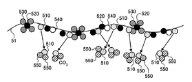
次に、本実施形態のプラズマ処理のモデルについて説明する。図5A〜図5Cは、本実施形態のプラズマ処理のモデルを示す図である。図5A〜図5Cにおいて、分子モデル群510は、ウェハWがエッチングされた後に電極板51に付着したカーボン含有物に含まれる炭素のモデルを示している。また、図5A〜図5Cにおいて、分子モデル群520は、ウェハWがエッチングされた後に電極板51に付着したチタン含有物(例えばTiF4、TiN、TiO2及びTi等)に含まれるチタンのモデルを示している。また、図5A〜図5Cにおいて、分子モデル群530は、ウェハWがエッチングされた後に電極板51に付着したチタン含有物(例えばTiF4等)に含まれるフッ素のモデルを示している。また、図5A〜図5Cにおいて、分子モデル群540は、ウェハWがエッチングされた後に電極板51に付着したチタン含有物(例えばTiN等)に含まれる窒素のモデルを示している。また、図5Bにおいて、分子モデル群550は、酸素のモデルを示している。
Next, the plasma processing model of this embodiment will be described. 5A to 5C are diagrams showing a plasma processing model of the present embodiment. 5A to 5C, a
本実施形態のプラズマ処理は、まず、第1のフッ素含有ガス(例えばC4F8ガス)をプラズマ処理空間Sに供給し、第1のフッ素含有ガスのプラズマを用いてウェハWをエッチングする第1の工程を実行する。これにより、図5Aに示すように、電極板51の表面には、エッチングされたウェハWの絶縁膜から生じたカーボン含有物(分子モデル群510)が付着するとともに、エッチングされたウェハWのマスク膜から生じたチタン含有物(分子モデル群520、分子モデル群530及び分子モデル群540)が付着する。このため、第1の工程は、「エッチング工程」ということができる。
In the plasma processing of the present embodiment, first, a first fluorine-containing gas (for example, C 4 F 8 gas) is supplied to the plasma processing space S, and the wafer W is etched using the plasma of the first fluorine-containing gas.
本実施形態のプラズマ処理は、O2ガスをプラズマ処理空間Sに供給し、電極板51に対して上記の第1の工程の後に付着したカーボン含有物をO2ガスのプラズマを用いて除去する第2の工程を実行する。これにより、図5Bに示すように、電極板51の表面におけるカーボン含有物とO2ガスのプラズマとが化学的に反応してCOやCO2となり、電極板51の表面からカーボン含有物が除去され、電極板51の表面におけるチタン含有物が露出される。このため、第2の工程は、「カーボン含有物除去工程」ということができる。
In the plasma processing of the present embodiment, O 2 gas is supplied to the plasma processing space S, and the carbon-containing material adhering to the
本実施形態のプラズマ処理は、窒素含有ガス(例えばN2ガス又はNF3ガス)及び第2のフッ素含有ガス(例えばCF4ガス、C4F8ガス又はCHF3ガス)をプラズマ処理空間Sに供給し、電極板51に対して上記の第1の工程の後に付着したチタン含有物を窒素含有ガス及び第2のフッ素含有ガスのプラズマを用いて除去する第3の工程を実行する。これにより、図5Cに示すように、電極板51の表面におけるチタン含有物と窒素含有ガス及び第2のフッ素含有ガスのプラズマとが化学的に反応してTi(NF3)等の錯体ガスが発生し、電極板51の表面からチタン含有物が除去される。このため、第3の工程は、「チタン含有物除去工程」ということができる。
In the plasma processing of this embodiment, a nitrogen-containing gas (for example, N 2 gas or NF 3 gas) and a second fluorine-containing gas (for example, CF 4 gas, C 4 F 8 gas, or CHF 3 gas) are applied to the plasma processing space S. The third step of supplying and removing the titanium-containing material attached to the
以上のように、本実施形態のプラズマ処理及びプラズマ処理装置1は、第1の工程で第1のフッ素含有ガスを供給し、第1のフッ素含有ガスを用いてウェハWをエッチングする。そして、本実施形態のプラズマ処理及びプラズマ処理装置1は、第2の工程でO2ガスをプラズマ処理空間Sに供給し、電極板51に対して第1の工程の後に付着したカーボン含有物をO2ガスのプラズマを用いて除去することにより、電極板51の表面におけるチタン含有物を露出させる。そして、本実施形態のプラズマ処理及びプラズマ処理装置1は、第3の工程で窒素含有ガス及び第2のフッ素含有ガスをプラズマ処理空間Sに供給し、電極板51に対して第1の工程の後に付着したチタン含有物を窒素含有ガス及び第2のフッ素含有ガスのプラズマを用いて除去することにより、Ti(NF3)等の錯体ガスを発生させる。このため、本実施形態によれば、エッチング時にウェハWから生じたチタン含有物等の付着物がプラズマ処理空間に対面する各種部材に付着した場合でも、各種部材から付着物を除去することができるので、プラズマ処理空間内のプラズマ密度の変動を抑えることが可能となる。その結果、本実施形態によれば、ウェハWのエッチング特性の経時劣化を抑制することができる。
As described above, the plasma processing and
次に、プラズマ処理の実施例について説明する。図6は、第1実施例のプラズマ処理のフローチャートを示す図である。 Next, an example of plasma processing will be described. FIG. 6 is a flowchart of the plasma processing of the first embodiment.
まず、第1実施例のプラズマ処理では、エッチング工程を実行する(ステップS101)。具体的には、制御部150は、流量調整機構74aを制御して、第1のフッ素含有ガスをプラズマ処理空間Sへ供給する。そして、制御部150は、第1の高周波電源30及び第2の高周波電源40を制御して、第1のフッ素含有ガスをプラズマ化させ、第1のフッ素含有ガスのプラズマを用いてウェハWをエッチングする。
First, in the plasma processing of the first embodiment, an etching process is executed (step S101). Specifically, the
続いて、第1実施例のプラズマ処理では、カーボン含有物除去工程を実行する(ステップS102)。具体的には、制御部150は、流量調整機構74bを制御して、O2ガスをプラズマ処理空間Sへ供給する。そして、制御部150は、第1の高周波電源30及び第2の高周波電源40を制御して、O2ガスをプラズマ化させ、プラズマ処理空間Sに表面を対向させて配置された電極板51に対して付着したカーボン含有物をO2ガスのプラズマを用いて除去する。
Subsequently, in the plasma treatment of the first embodiment, a carbon-containing material removal step is executed (step S102). Specifically, the
続いて、第1実施例のプラズマ処理では、チタン含有物除去工程を実行する(ステップS103)。具体的には、制御部150は、流量調整機構74c及び流量調整機構74dをそれぞれ制御して、窒素含有ガス及び第2のフッ素含有ガスをプラズマ処理空間Sへ供給する。そして、制御部150は、第1の高周波電源30及び第2の高周波電源40を制御して、窒素含有ガス及び第2のフッ素含有ガスをプラズマ化させ、プラズマ処理空間Sに表面を対向させて配置された電極板51に対して付着したチタン含有物を窒素含有ガス及び第2のフッ素含有ガスを用いて除去する。
Subsequently, in the plasma treatment of the first embodiment, a titanium-containing material removal step is executed (step S103). Specifically, the
第1実施例のプラズマ処理によれば、エッチング工程を行うことによりウェハWをエッチングし、その後カーボン含有物除去工程を行うことにより電極板51に付着したカーボン含有物を除去してチタン含有物を露出させ、その後チタン含有物除去工程を行うことによりTi(NF3)等の錯体ガスとしてチタン含有物を除去することができる。このため、エッチング時にウェハWから生じたチタン含有物等の付着物が電極板51に付着した場合でも、付着物のうちチタン含有物を効率良く除去することができるので、プラズマ処理空間内のプラズマ密度の変動を抑えることが可能となる。その結果、ウェハWのエッチング特性の経時変動を抑制することができる。
According to the plasma treatment of the first embodiment, the etching process is performed to etch the wafer W, and then the carbon content removal process is performed to remove the carbon content adhering to the
次に、第2実施例のプラズマ処理について説明する。図7は、第2実施例のプラズマ処理のフローチャートを示す図である。 Next, the plasma processing of the second embodiment will be described. FIG. 7 is a diagram showing a flowchart of the plasma processing of the second embodiment.
まず、第2実施例のプラズマ処理では、エッチング工程を実行する(ステップS201)。具体的には、制御部150は、流量調整機構74aを制御して、第1のフッ素含有ガスをプラズマ処理空間Sへ供給する。そして、制御部150は、第1の高周波電源30及び第2の高周波電源40を制御して、第1のフッ素含有ガスをプラズマ化させ、第1のフッ素含有ガスのプラズマを用いてウェハWをエッチングする。
First, in the plasma processing of the second embodiment, an etching process is executed (step S201). Specifically, the
続いて、第2実施例のプラズマ処理では、チタン含有物除去工程を実行する(ステップS202)。具体的には、制御部150は、流量調整機構74c及び流量調整機構74dをそれぞれ制御して、窒素含有ガス及び第2のフッ素含有ガスをプラズマ処理空間Sへ供給する。そして、制御部150は、第1の高周波電源30及び第2の高周波電源40を制御して、窒素含有ガス及び第2のフッ素含有ガスをプラズマ化させ、プラズマ処理空間Sに表面を対向させて配置された電極板51に対して付着したチタン含有物を窒素含有ガス及び第2のフッ素含有ガスを用いて除去する。
Subsequently, in the plasma treatment of the second embodiment, a titanium-containing material removal step is executed (step S202). Specifically, the
続いて、第2実施例のプラズマ処理では、カーボン含有物除去工程を実行する(ステップS203)。具体的には、制御部150は、流量調整機構74bを制御して、O2ガスをプラズマ処理空間Sへ供給する。そして、制御部150は、第1の高周波電源30及び第2の高周波電源40を制御して、O2ガスをプラズマ化させ、プラズマ処理空間Sに表面を対向させて配置された電極板51に対して付着したカーボン含有物をO2ガスのプラズマを用いて除去する。
Subsequently, in the plasma treatment of the second embodiment, a carbon-containing material removal step is executed (step S203). Specifically, the
第2実施例のプラズマ処理によれば、エッチング工程を行うことによりウェハWをエッチングし、その後チタン含有物除去工程を行うことにより電極板51に付着したチタン含有物をTi(NF3)等の錯体ガスとして除去してカーボン含有物を露出させ、その後カーボン含有物除去工程を行うことによりカーボン含有物を除去することができる。このため、エッチング時にウェハWから生じたチタン含有物等の付着物が電極板51に付着した場合でも、付着物のうちチタン含有物を効率良く除去することができるので、プラズマ処理空間内のプラズマ密度の変動を抑えることが可能となる。その結果、ウェハWのエッチング特性の経時変動を抑制することができる。
According to the plasma treatment of the second embodiment, the wafer W is etched by performing an etching process, and then the titanium-containing material attached to the
次に、第3実施例のプラズマ処理について説明する。図8は、第3実施例のプラズマ処理のフローチャートを示す図である。 Next, the plasma processing of the third embodiment will be described. FIG. 8 is a flowchart of the plasma processing according to the third embodiment.
まず、第3実施例のプラズマ処理では、エッチング工程を実行する(ステップS301)。具体的には、制御部150は、流量調整機構74aを制御して、第1のフッ素含有ガスをプラズマ処理空間Sへ供給する。そして、制御部150は、第1の高周波電源30及び第2の高周波電源40を制御して、第1のフッ素含有ガスをプラズマ化させ、第1のフッ素含有ガスのプラズマを用いてウェハWをエッチングする。
First, in the plasma processing of the third embodiment, an etching process is executed (step S301). Specifically, the
続いて、第3実施例のプラズマ処理では、第1のカーボン含有物除去工程を実行する(ステップS302)。具体的には、制御部150は、流量調整機構74bを制御して、O2ガスをプラズマ処理空間Sへ供給する。そして、制御部150は、第1の高周波電源30及び第2の高周波電源40を制御して、O2ガスをプラズマ化させ、プラズマ処理空間Sに表面を対向させて配置された電極板51に対して付着したカーボン含有物をO2ガスのプラズマを用いて除去する。
Subsequently, in the plasma processing of the third embodiment, a first carbon-containing material removal step is executed (step S302). Specifically, the
続いて、第3実施例のプラズマ処理では、第1のチタン含有物除去工程を実行する(ステップS303)。具体的には、制御部150は、流量調整機構74c及び流量調整機構74dをそれぞれ制御して、窒素含有ガス及び第2のフッ素含有ガスをプラズマ処理空間Sへ供給する。そして、制御部150は、第1の高周波電源30及び第2の高周波電源40を制御して、窒素含有ガス及び第2のフッ素含有ガスをプラズマ化させ、プラズマ処理空間Sに表面を対向させて配置された電極板51に対して付着したチタン含有物を窒素含有ガス及び第2のフッ素含有ガスのプラズマを用いて除去する。
Subsequently, in the plasma treatment of the third embodiment, a first titanium-containing material removal step is executed (step S303). Specifically, the
続いて、第3実施例のプラズマ処理では、第2のカーボン含有物除去工程を実行する(ステップS304)。具体的には、制御部150は、流量調整機構74bを制御して、O2ガスをプラズマ処理空間Sへ供給する。そして、制御部150は、第1の高周波電源30及び第2の高周波電源40を制御して、O2ガスをプラズマ化させ、プラズマ処理空間Sに表面を対向させて配置された電極板51に対して付着したカーボン含有物をO2ガスのプラズマを用いて除去する。
Subsequently, in the plasma treatment of the third embodiment, a second carbon-containing material removal step is executed (step S304). Specifically, the
続いて、第3実施例のプラズマ処理では、第2のチタン含有物除去工程を実行する(ステップS305)。具体的には、制御部150は、流量調整機構74c及び流量調整機構74dをそれぞれ制御して、窒素含有ガス及び第2のフッ素含有ガスをプラズマ処理空間Sへ供給する。そして、制御部150は、第1の高周波電源30及び第2の高周波電源40を制御して、窒素含有ガス及び第2のフッ素含有ガスをプラズマ化させ、プラズマ処理空間Sに表面を対向させて配置された電極板51に対して付着したチタン含有物を窒素含有ガス及び第2のフッ素含有ガスのプラズマを用いて除去する。
Subsequently, in the plasma treatment of the third embodiment, a second titanium-containing material removal step is executed (step S305). Specifically, the
第3実施例のプラズマ処理によれば、第1実施例と同様に、エッチング工程を行うことによりウェハWをエッチングし、その後カーボン含有物除去工程を行うことにより電極板51に付着したカーボン含有物を除去してチタン含有物を露出させ、その後チタン含有物除去工程を行うことによりTi(NF3)等の錯体ガスとしてチタン含有物を除去することができる。このため、エッチング時にウェハWから生じたチタン含有物等の付着物が電極板51に付着した場合でも、付着物のうちチタン含有物を効率良く除去することができるので、プラズマ処理空間内のプラズマ密度の変動を抑えることが可能となる。その結果、ウェハWのエッチング特性の経時変動を抑制することができる。また、第3実施例のプラズマ処理によれば、エッチング工程を実行した後にカーボン含有物除去工程とチタン含有物除去工程とのセットを2回繰り返して実行しているので、電極板51に付着した付着物をより効率良く除去することができる。なお、第3実施例では、エッチング工程を実行した後にカーボン含有物除去工程とチタン含有物除去工程とのセットを2回繰り返して実行する例を示したが、エッチング工程を実行した後にカーボン含有物除去工程とチタン含有物除去工程とのセットを2回以上繰り返して実行してもよい。
According to the plasma treatment of the third embodiment, similarly to the first embodiment, the wafer W is etched by performing the etching step, and then the carbon-containing material attached to the
次に、第4実施例のプラズマ処理について説明する。図9は、第4実施例のプラズマ処理のフローチャートを示す図である。 Next, plasma processing according to the fourth embodiment will be described. FIG. 9 is a view showing a flowchart of the plasma processing of the fourth embodiment.
まず、第4実施例のプラズマ処理では、エッチング工程を実行する(ステップS401)。具体的には、制御部150は、流量調整機構74aを制御して、第1のフッ素含有ガスをプラズマ処理空間Sへ供給する。そして、制御部150は、第1の高周波電源30及び第2の高周波電源40を制御して、第1のフッ素含有ガスをプラズマ化させ、第1のフッ素含有ガスのプラズマを用いてウェハWをエッチングする。
First, in the plasma processing of the fourth embodiment, an etching process is executed (step S401). Specifically, the
続いて、第4実施例のプラズマ処理では、カーボン含有物除去工程を実行する(ステップS402)。具体的には、制御部150は、流量調整機構74bを制御して、O2ガスをプラズマ処理空間Sへ供給する。そして、制御部150は、第1の高周波電源30及び第2の高周波電源40を制御して、O2ガスをプラズマ化させ、プラズマ処理空間Sに表面を対向させて配置された電極板51に対して付着したカーボン含有物をO2ガスのプラズマを用いて除去する。
Subsequently, in the plasma treatment of the fourth embodiment, a carbon-containing material removal step is executed (step S40 2 ). Specifically, the
続いて、第4実施例のプラズマ処理では、CHF3ガスを用いたチタン含有物除去工程を実行する(ステップS403)。具体的には、制御部150は、流量調整機構74d等を制御して、第3のフッ素含有ガスとしてCHF3ガスをプラズマ処理空間Sへ供給する。そして、制御部150は、第1の高周波電源30及び第2の高周波電源40を制御して、CHF3ガスをプラズマ化させ、プラズマ処理空間Sに表面を対向させて配置された電極板51に対して付着したチタン含有物をCHF3ガスのプラズマを用いて除去する。
Subsequently, in the plasma treatment of the fourth embodiment, a titanium-containing material removal step using CHF 3 gas is executed (step S403). Specifically, the
続いて、第4実施例のプラズマ処理では、チタン含有物除去工程を実行する(ステップS404)。具体的には、制御部150は、流量調整機構74c及び流量調整機構74dをそれぞれ制御して、窒素含有ガス及び第2のフッ素含有ガスをプラズマ処理空間Sへ供給する。そして、制御部150は、第1の高周波電源30及び第2の高周波電源40を制御して、窒素含有ガス及び第2のフッ素含有ガスをプラズマ化させ、プラズマ処理空間Sに表面を対向させて配置された電極板51に対して付着したチタン含有物を窒素含有ガス及び第2のフッ素含有ガスのプラズマを用いて除去する。
Subsequently, in the plasma treatment of the fourth embodiment, a titanium-containing material removal step is executed (step S404). Specifically, the
第4実施例のプラズマ処理によれば、第1実施例と同様に、エッチング工程を行うことによりウェハWをエッチングし、その後カーボン含有物除去工程を行うことにより電極板51に付着したカーボン含有物を除去してチタン含有物を露出させ、その後チタン含有物除去工程を行うことによりTi(NF3)等の錯体ガスとしてチタン含有物を除去することができる。このため、エッチング時にウェハWから生じたチタン含有物等の付着物が電極板51に付着した場合でも、付着物のうちチタン含有物を効率良く除去することができるので、プラズマ処理空間内のプラズマ密度の変動を抑えることが可能となる。その結果、ウェハWのエッチング特性の経時変動を抑制することができる。また、第4実施例のプラズマ処理によれば、カーボン含有物除去工程とチタン含有物除去工程との間に、第3のフッ素含有ガスとしてのCHF3ガスをプラズマ処理空間に供給し、電極板51に付着したチタン含有物をCHF3ガスのプラズマを用いて除去するので、電極板51に付着した付着物をより効率良く除去することができる。
According to the plasma treatment of the fourth embodiment, as in the first embodiment, the wafer W is etched by performing the etching process, and then the carbon-containing material attached to the
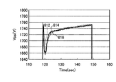
次に、本実施形態のプラズマ処理方法による効果について説明する。図10A及び図10Bは、本実施形態のプラズマ処理方法による効果を説明するための図(その1)である。図10A及び図10Bは、プラズマ処理装置1によってウェハWに対してプラズマ処理を行った場合における効果を示す図である。図10A及び図10Bにおいて、横軸は、プラズマ処理装置1によってウェハWに対してプラズマ処理を行った時間(sec)を示し、縦軸は、ウェハWのVpp(V)を示している。なお、Vppは、ウェハWの表面における高周波電力の電圧値の最大値と最小値との差である。このVppは、高周波電力によるプラズマ密度と相関があることがわかっており、このVpp(V)の変動がすなわちプラズマ密度の変動と言える。
Next, the effect by the plasma processing method of this embodiment is demonstrated. FIG. 10A and FIG. 10B are views (No. 1) for explaining the effect of the plasma processing method of the present embodiment. 10A and 10B are diagrams showing effects when the
また、図10Aは、本実施形態のプラズマ処理方法を用いることなく、ウェハWにO2ガスのプラズマを用いたドライクリーニング(DC:Dry Cleaning)処理を実行した場合の、DC処理時のロット番号毎のウェハWのVppと時間との関係を示すグラフである。つまり、図10Aにおいて、グラフ602は、ロット番号「1」のウエハW25枚に対してデュアルダマシン配線用の溝のエッチング(図2参照)を行い、その後にDC処理を行ったときのVppと時間との関係を示す。グラフ604は、ロット番号「2」のウェハW25枚処理後(ロット番号「1」を含んだ累積でウエハW50枚処理後)のDC処理におけるVppと時間との関係を示す。また、グラフ606は、ロット番号「3」のウェハW25枚処理後(ロット番号「1」及び「2」を含んだ累積でウエハW75枚処理後)のDC処理におけるVppと時間との関係を示している。一方、図10Bは、本実施形態のプラズマ処理方法を用いてウェハWに対してプラズマ処理を実行した場合の、ロット番号毎のウェハWのVppと時間との関係を示すグラフである。つまり、図10Bにおいて、グラフ612は、ロット番号「1」のウエハW25枚に対してデュアルダマシン配線用の溝のエッチング(図2参照)を行った後に、本実施形態のプラズマ処理を行い、その後にDC処理を行ったときのVppと時間との関係を示す。言い換えると、グラフ612は、図10AのDC処理の前に、本実施形態のプラズマ処理を行った場合の効果を示す図となっている。グラフ614は、ロット番号「2」のウェハW25枚処理後(ロット番号「1」を含んだ累積でウエハW50枚処理後)に、本実施形態のプラズマ処理を行い、その後のDC処理におけるVppと時間との関係を示しており、グラフ616は、ロット番号「3」のウェハW25枚処理後(ロット番号「1」及び「2」を含んだ累積でウエハW75枚処理後)に、本実施形態のプラズマ処理を行い、その後のDC処理におけるVppと時間との関係を示している。
FIG. 10A shows a lot number at the time of DC processing when dry cleaning (DC) processing using plasma of O 2 gas is performed on the wafer W without using the plasma processing method of the present embodiment. It is a graph which shows the relationship between Vpp of every wafer W, and time. That is, in FIG. 10A, a
まず、図10Aに示すように、本実施形態のプラズマ処理方法を用いることなく単にDC処理を実行した場合、グラフ602,604,606に示すように、ロット番号の相違によって、ウェハWのVppの時間に対する履歴は異なっている。これは、エッチング時にウェハWのマスク膜から生じたチタン含有物が、プラズマ処理空間に対面する電極板51に累積的に付着してプラズマ処理空間内のプラズマ密度が変動したためであると考えられる。
First, as shown in FIG. 10A, when the DC process is simply executed without using the plasma processing method of the present embodiment, the difference in the lot number causes the difference in Vpp of the wafer W as shown in
これに対して、本実施形態のプラズマ処理方法を用いてウェハWに対してプラズマ処理を実行した場合、カーボン含有物除去工程を行うことにより電極板51に付着したカーボン含有物を除去するとともに、チタン含有物除去工程を行うことにより電極板51に付着したチタン含有物を除去する。その結果、DC処理時の図10Bのグラフ612,614,616に示すように、ロット番号に関わらず、ウェハWのVppの時間に対する履歴は同等に維持されている。これは、エッチング時にウェハWのマスク膜から生じたチタン含有物が、プラズマ処理空間に対面する電極板51に付着した場合でも、電極板51に付着したチタン含有物が除去されたためであると考えられる。つまり、プラズマ密度の変動が抑制されていることがわかる。
On the other hand, when the plasma processing is performed on the wafer W using the plasma processing method of the present embodiment, the carbon-containing material attached to the
図11は、本実施形態のプラズマ処理方法による効果を説明するための図(その2)である。図11において、横軸は、プラズマ処理装置1へ搬入されたウェハWのロット番号(累積した値)を示し、縦軸は、ウェハWの絶縁膜をエッチングした場合に絶縁膜に形成される溝の溝径(nm)を示している。
FIG. 11 is a diagram (No. 2) for explaining the effect of the plasma processing method of the present embodiment. In FIG. 11, the horizontal axis indicates the lot number (accumulated value) of the wafer W carried into the
また、図11において、グラフ702は、本実施形態のプラズマ処理方法を用いることなく、DC処理のみを実行した場合に絶縁膜に形成される溝の溝径の、ロット番号(累積した値)に対する変動を示している。また、図11において、グラフ704は、本実施形態のプラズマ処理方法を実行した場合に絶縁膜に形成される溝の溝径の、ロット番号に対する変動を示している。
In FIG. 11, a
グラフ702とグラフ704とを比較すると、本実施形態のプラズマ処理方法を実行した場合に絶縁膜に形成される溝の溝径の、ロット番号に対する減少幅は、DC処理のみを実行した場合に絶縁膜に形成される溝の溝径の、ロット番号に対する減少幅よりも小さい。これは、本実施形態のプラズマ処理方法を実行した場合には、エッチング時にウェハWのマスク膜から生じたチタン含有物が、プラズマ処理空間に対面する電極板51に付着した場合でも、電極板51に付着したチタン含有物が除去されたためであると考えられる。その結果、プラズマ密度が安定しエッチングした溝の形状の変動も抑制されていることがわかる。
Comparing the
1 プラズマ処理装置
11 処理容器
20 フォーカスリング
30 第1の高周波電源
40 第2の高周波電源
42 上部電極
51 電極板
52 電極支持体
72 処理ガス供給源
72a、72b、72c、72d ガス供給部
74a、74b、74c、74d 流量調整機構
150 制御部
D1 絶縁膜
D2 マスク膜
S プラズマ処理空間
W ウェハ
DESCRIPTION OF
Claims (5)
第1のフッ素含有ガスをプラズマ処理空間に供給し、絶縁膜の表面にチタン含有物のマスク膜が形成された被処理基板を前記第1のフッ素含有ガスのプラズマを用いてエッチングする第1の工程と、
O2ガスを前記プラズマ処理空間に供給し、前記プラズマ処理空間に表面を対向させて配置された部材に対して前記第1の工程の後に付着したカーボン含有物を前記O2ガスのプラズマを用いて除去する第2の工程と、
窒素含有ガス及び第2のフッ素含有ガスを前記プラズマ処理空間に供給し、前記部材に対して前記第1の工程の後に付着したチタン含有物を前記窒素含有ガス及び前記第2のフッ素含有ガスのプラズマを用いて除去する第3の工程と
を含むことを特徴とするプラズマ処理方法。 A plasma processing method in a plasma processing apparatus,
A first fluorine-containing gas is supplied to the plasma processing space, and a substrate to be processed having a titanium-containing material mask film formed on the surface of the insulating film is etched using the first fluorine-containing gas plasma. Process,
O 2 gas is supplied to the plasma processing space, and the carbon-containing material attached after the first step to the member disposed with the surface facing the plasma processing space is used for the plasma of the O 2 gas. A second step of removing by
A nitrogen-containing gas and a second fluorine-containing gas are supplied to the plasma processing space, and the titanium-containing material attached to the member after the first step is removed from the nitrogen-containing gas and the second fluorine-containing gas. And a third step of removing using plasma.
前記第1の工程を実行した後に前記第2の工程及び前記第3の工程を少なくとも2回繰り返して実行することを特徴とする請求項1又は請求項2に記載のプラズマ処理方法。 The plasma processing apparatus is
3. The plasma processing method according to claim 1, wherein the second process and the third process are repeatedly performed at least twice after the first process is performed.
第1のフッ素含有ガスを前記プラズマ処理空間に供給する第1のガス供給部と、
O2ガスを前記プラズマ処理空間に供給する第2のガス供給部と、
窒素含有ガス及び第2のフッ素含有ガスを前記プラズマ処理空間に供給する第3のガス供給部と、
前記第1のガス供給部から前記第1のフッ素含有ガスを前記プラズマ処理空間に供給し、前記第1のフッ素含有ガスのプラズマを用いて前記被処理基板をエッチングする第1の工程と、前記第2のガス供給部から前記O2ガスを前記プラズマ処理空間に供給し、前記プラズマ処理空間に表面を対向させて配置された部材に対して前記第1の工程の後に付着したカーボン含有物を前記O2ガスのプラズマを用いて除去する第2の工程と、前記第3のガス供給部から前記窒素含有ガス及び前記第2のフッ素含有ガスを前記プラズマ処理空間に供給し、前記部材に対して前記第1の工程の後に付着したチタン含有物を前記窒素含有ガス及び前記第2のフッ素含有ガスのプラズマを用いて除去する第3の工程とを実行する制御部と
を備えたことを特徴とするプラズマ処理装置。 A processing container that defines a plasma processing space in which a substrate to be processed in which a mask film of titanium-containing material is formed on the surface of the insulating film is disposed;
A first gas supply unit for supplying a first fluorine-containing gas to the plasma processing space;
A second gas supply unit for supplying O 2 gas to the plasma processing space;
A third gas supply unit for supplying a nitrogen-containing gas and a second fluorine-containing gas to the plasma processing space;
A first step of supplying the first fluorine-containing gas from the first gas supply unit to the plasma processing space and etching the substrate to be processed using the plasma of the first fluorine-containing gas; The O 2 gas is supplied from the second gas supply unit to the plasma processing space, and the carbon-containing material attached after the first step to the member disposed with the surface facing the plasma processing space A second step of removing the plasma using the O 2 gas; and supplying the nitrogen-containing gas and the second fluorine-containing gas from the third gas supply unit to the plasma processing space; And a third step of removing the titanium-containing material adhering after the first step by using the plasma of the nitrogen-containing gas and the second fluorine-containing gas. To plasma processing apparatus.
Priority Applications (7)
| Application Number | Priority Date | Filing Date | Title |
|---|---|---|---|
| JP2012186344A JP5982223B2 (en) | 2012-08-27 | 2012-08-27 | Plasma processing method and plasma processing apparatus |
| PCT/JP2013/071409 WO2014034396A1 (en) | 2012-08-27 | 2013-08-07 | Plasma processing method and plasma processing device |
| CN201380039947.7A CN104508803B (en) | 2012-08-27 | 2013-08-07 | Method of plasma processing |
| US14/424,217 US9460896B2 (en) | 2012-08-27 | 2013-08-07 | Plasma processing method and plasma processing apparatus |
| EP13833486.7A EP2879166B1 (en) | 2012-08-27 | 2013-08-07 | Plasma processing method |
| KR1020157005120A KR102114922B1 (en) | 2012-08-27 | 2013-08-07 | Plasma processing method |
| TW102130274A TWI571930B (en) | 2012-08-27 | 2013-08-23 | Plasma processing method and plasma processing device |
Applications Claiming Priority (1)
| Application Number | Priority Date | Filing Date | Title |
|---|---|---|---|
| JP2012186344A JP5982223B2 (en) | 2012-08-27 | 2012-08-27 | Plasma processing method and plasma processing apparatus |
Publications (3)
| Publication Number | Publication Date |
|---|---|
| JP2014045063A JP2014045063A (en) | 2014-03-13 |
| JP2014045063A5 JP2014045063A5 (en) | 2015-07-09 |
| JP5982223B2 true JP5982223B2 (en) | 2016-08-31 |
Family
ID=50183214
Family Applications (1)
| Application Number | Title | Priority Date | Filing Date |
|---|---|---|---|
| JP2012186344A Active JP5982223B2 (en) | 2012-08-27 | 2012-08-27 | Plasma processing method and plasma processing apparatus |
Country Status (7)
| Country | Link |
|---|---|
| US (1) | US9460896B2 (en) |
| EP (1) | EP2879166B1 (en) |
| JP (1) | JP5982223B2 (en) |
| KR (1) | KR102114922B1 (en) |
| CN (1) | CN104508803B (en) |
| TW (1) | TWI571930B (en) |
| WO (1) | WO2014034396A1 (en) |
Families Citing this family (9)
| Publication number | Priority date | Publication date | Assignee | Title |
|---|---|---|---|---|
| JP6049527B2 (en) * | 2013-04-05 | 2016-12-21 | 東京エレクトロン株式会社 | Plasma processing method and plasma processing apparatus |
| JP2017045849A (en) * | 2015-08-26 | 2017-03-02 | 東京エレクトロン株式会社 | Seasoning method and etching method |
| CN108292601A (en) * | 2016-01-13 | 2018-07-17 | 应用材料公司 | The cleaning based on hydrogen plasma for etching hardware |
| CN107369603A (en) * | 2016-05-12 | 2017-11-21 | 中芯国际集成电路制造(上海)有限公司 | Remove oxygen-containing accessory substance, etching chamber and the method for forming semiconductor structure |
| JP6763750B2 (en) * | 2016-11-07 | 2020-09-30 | 東京エレクトロン株式会社 | How to process the object to be processed |
| US10886468B2 (en) * | 2017-04-14 | 2021-01-05 | Sakai Display Products Corporation | Manufacturing method and manufacturing apparatus for organic EL display device |
| US11123845B2 (en) * | 2017-06-21 | 2021-09-21 | Hp Indigo B.V. | Vacuum tables |
| CN109962001A (en) * | 2017-12-26 | 2019-07-02 | 中微半导体设备(上海)股份有限公司 | A kind of operation method and plasma reactor of plasma chamber |
| WO2023137275A1 (en) * | 2022-01-13 | 2023-07-20 | Lam Research Corporation | High selectivity and uniform dielectric etch |
Family Cites Families (16)
| Publication number | Priority date | Publication date | Assignee | Title |
|---|---|---|---|---|
| JPH03239323A (en) * | 1990-02-16 | 1991-10-24 | Yamaha Corp | Dry etching method |
| JP3117187B2 (en) * | 1995-12-20 | 2000-12-11 | 株式会社日立製作所 | Plasma cleaning method |
| US5948702A (en) * | 1996-12-19 | 1999-09-07 | Texas Instruments Incorporated | Selective removal of TixNy |
| JPH10280151A (en) * | 1997-04-08 | 1998-10-20 | Fujitsu Ltd | Cleaning of cvd system |
| US6692903B2 (en) * | 2000-12-13 | 2004-02-17 | Applied Materials, Inc | Substrate cleaning apparatus and method |
| JP4176365B2 (en) * | 2002-03-25 | 2008-11-05 | 東京エレクトロン株式会社 | Plasma etching method |
| US20060016783A1 (en) * | 2004-07-22 | 2006-01-26 | Dingjun Wu | Process for titanium nitride removal |
| US7488689B2 (en) | 2004-12-07 | 2009-02-10 | Tokyo Electron Limited | Plasma etching method |
| JP2006165246A (en) * | 2004-12-07 | 2006-06-22 | Tokyo Electron Ltd | Plasma etching method |
| JP5047504B2 (en) | 2005-02-05 | 2012-10-10 | 三星電子株式会社 | Method for manufacturing dual damascene wiring of semiconductor device using via capping protective film |
| JP4764028B2 (en) * | 2005-02-28 | 2011-08-31 | 株式会社日立ハイテクノロジーズ | Plasma processing method |
| JP4288252B2 (en) * | 2005-04-19 | 2009-07-01 | パナソニック株式会社 | Manufacturing method of semiconductor chip |
| JP2008198659A (en) * | 2007-02-08 | 2008-08-28 | Tokyo Electron Ltd | Plasma etching method |
| JP5705495B2 (en) * | 2010-10-07 | 2015-04-22 | 株式会社日立ハイテクノロジーズ | Plasma processing method and plasma processing apparatus |
| US20120094499A1 (en) * | 2010-10-15 | 2012-04-19 | Siu Tang Ng | Method of performing an in situ chamber clean |
| JP6177601B2 (en) * | 2013-06-25 | 2017-08-09 | 東京エレクトロン株式会社 | Cleaning method and substrate processing apparatus |
-
2012
- 2012-08-27 JP JP2012186344A patent/JP5982223B2/en active Active
-
2013
- 2013-08-07 CN CN201380039947.7A patent/CN104508803B/en active Active
- 2013-08-07 US US14/424,217 patent/US9460896B2/en active Active
- 2013-08-07 KR KR1020157005120A patent/KR102114922B1/en active IP Right Grant
- 2013-08-07 WO PCT/JP2013/071409 patent/WO2014034396A1/en active Application Filing
- 2013-08-07 EP EP13833486.7A patent/EP2879166B1/en active Active
- 2013-08-23 TW TW102130274A patent/TWI571930B/en active
Also Published As
| Publication number | Publication date |
|---|---|
| US9460896B2 (en) | 2016-10-04 |
| TWI571930B (en) | 2017-02-21 |
| KR102114922B1 (en) | 2020-05-25 |
| EP2879166A4 (en) | 2016-03-16 |
| CN104508803A (en) | 2015-04-08 |
| EP2879166B1 (en) | 2019-10-09 |
| WO2014034396A1 (en) | 2014-03-06 |
| JP2014045063A (en) | 2014-03-13 |
| CN104508803B (en) | 2016-12-07 |
| TW201413817A (en) | 2014-04-01 |
| US20150228458A1 (en) | 2015-08-13 |
| EP2879166A1 (en) | 2015-06-03 |
| KR20150048134A (en) | 2015-05-06 |
Similar Documents
| Publication | Publication Date | Title |
|---|---|---|
| JP5982223B2 (en) | Plasma processing method and plasma processing apparatus | |
| JP6035117B2 (en) | Plasma etching method and plasma etching apparatus | |
| JP2008028022A (en) | Plasma etching method and computer readable storage medium | |
| JP2019207911A (en) | Method of etching film and plasma processing apparatus | |
| US11462412B2 (en) | Etching method | |
| JPWO2014046083A1 (en) | Plasma etching method and plasma etching apparatus | |
| US9147556B2 (en) | Plasma processing method and plasma processing apparatus | |
| US9818582B2 (en) | Plasma processing method | |
| JP6811202B2 (en) | Etching method and plasma processing equipment | |
| JP6494424B2 (en) | Etching method | |
| JP6063181B2 (en) | Plasma processing method and plasma processing apparatus | |
| US20160032445A1 (en) | Plasma processing apparatus and plasma processing method | |
| JP6235471B2 (en) | Seasoning method, plasma processing apparatus, and manufacturing method | |
| JP5704192B2 (en) | Plasma etching method, plasma etching apparatus, and storage medium | |
| JP2019117876A (en) | Etching method | |
| JP2006165246A (en) | Plasma etching method | |
| CN111326395A (en) | Plasma processing method and plasma processing apparatus | |
| WO2023008025A1 (en) | Etching method, method for manufacturing semiconductor device, etching program, and plasma processing device | |
| TWI802266B (en) | Etching method, manufacturing method of semiconductor device, and plasma processing device | |
| JP2010166092A (en) | Method for plasma etching |
Legal Events
| Date | Code | Title | Description |
|---|---|---|---|
| A521 | Request for written amendment filed |
Free format text: JAPANESE INTERMEDIATE CODE: A523 Effective date: 20150525 |
|
| A621 | Written request for application examination |
Free format text: JAPANESE INTERMEDIATE CODE: A621 Effective date: 20150525 |
|
| TRDD | Decision of grant or rejection written | ||
| A01 | Written decision to grant a patent or to grant a registration (utility model) |
Free format text: JAPANESE INTERMEDIATE CODE: A01 Effective date: 20160712 |
|
| A61 | First payment of annual fees (during grant procedure) |
Free format text: JAPANESE INTERMEDIATE CODE: A61 Effective date: 20160801 |
|
| R150 | Certificate of patent or registration of utility model |
Ref document number: 5982223 Country of ref document: JP Free format text: JAPANESE INTERMEDIATE CODE: R150 |
|
| R250 | Receipt of annual fees |
Free format text: JAPANESE INTERMEDIATE CODE: R250 |
|
| R250 | Receipt of annual fees |
Free format text: JAPANESE INTERMEDIATE CODE: R250 |
|
| R250 | Receipt of annual fees |
Free format text: JAPANESE INTERMEDIATE CODE: R250 |
|
| R250 | Receipt of annual fees |
Free format text: JAPANESE INTERMEDIATE CODE: R250 |
|
| R250 | Receipt of annual fees |
Free format text: JAPANESE INTERMEDIATE CODE: R250 |