JP5908962B2 - Method for preparing conductive composite material - Google Patents
Method for preparing conductive composite material Download PDFInfo
- Publication number
- JP5908962B2 JP5908962B2 JP2014243279A JP2014243279A JP5908962B2 JP 5908962 B2 JP5908962 B2 JP 5908962B2 JP 2014243279 A JP2014243279 A JP 2014243279A JP 2014243279 A JP2014243279 A JP 2014243279A JP 5908962 B2 JP5908962 B2 JP 5908962B2
- Authority
- JP
- Japan
- Prior art keywords
- group
- composite material
- composite
- metal nanoparticles
- nanoparticles
- Prior art date
- Legal status (The legal status is an assumption and is not a legal conclusion. Google has not performed a legal analysis and makes no representation as to the accuracy of the status listed.)
- Expired - Fee Related
Links
Images


Classifications
-
- B—PERFORMING OPERATIONS; TRANSPORTING
- B22—CASTING; POWDER METALLURGY
- B22F—WORKING METALLIC POWDER; MANUFACTURE OF ARTICLES FROM METALLIC POWDER; MAKING METALLIC POWDER; APPARATUS OR DEVICES SPECIALLY ADAPTED FOR METALLIC POWDER
- B22F9/00—Making metallic powder or suspensions thereof
- B22F9/16—Making metallic powder or suspensions thereof using chemical processes
- B22F9/18—Making metallic powder or suspensions thereof using chemical processes with reduction of metal compounds
- B22F9/24—Making metallic powder or suspensions thereof using chemical processes with reduction of metal compounds starting from liquid metal compounds, e.g. solutions
-
- H—ELECTRICITY
- H01—ELECTRIC ELEMENTS
- H01B—CABLES; CONDUCTORS; INSULATORS; SELECTION OF MATERIALS FOR THEIR CONDUCTIVE, INSULATING OR DIELECTRIC PROPERTIES
- H01B1/00—Conductors or conductive bodies characterised by the conductive materials; Selection of materials as conductors
- H01B1/20—Conductive material dispersed in non-conductive organic material
- H01B1/22—Conductive material dispersed in non-conductive organic material the conductive material comprising metals or alloys
-
- C—CHEMISTRY; METALLURGY
- C09—DYES; PAINTS; POLISHES; NATURAL RESINS; ADHESIVES; COMPOSITIONS NOT OTHERWISE PROVIDED FOR; APPLICATIONS OF MATERIALS NOT OTHERWISE PROVIDED FOR
- C09C—TREATMENT OF INORGANIC MATERIALS, OTHER THAN FIBROUS FILLERS, TO ENHANCE THEIR PIGMENTING OR FILLING PROPERTIES ; PREPARATION OF CARBON BLACK ; PREPARATION OF INORGANIC MATERIALS WHICH ARE NO SINGLE CHEMICAL COMPOUNDS AND WHICH ARE MAINLY USED AS PIGMENTS OR FILLERS
- C09C1/00—Treatment of specific inorganic materials other than fibrous fillers; Preparation of carbon black
- C09C1/62—Metallic pigments or fillers
-
- C—CHEMISTRY; METALLURGY
- C09—DYES; PAINTS; POLISHES; NATURAL RESINS; ADHESIVES; COMPOSITIONS NOT OTHERWISE PROVIDED FOR; APPLICATIONS OF MATERIALS NOT OTHERWISE PROVIDED FOR
- C09C—TREATMENT OF INORGANIC MATERIALS, OTHER THAN FIBROUS FILLERS, TO ENHANCE THEIR PIGMENTING OR FILLING PROPERTIES ; PREPARATION OF CARBON BLACK ; PREPARATION OF INORGANIC MATERIALS WHICH ARE NO SINGLE CHEMICAL COMPOUNDS AND WHICH ARE MAINLY USED AS PIGMENTS OR FILLERS
- C09C3/00—Treatment in general of inorganic materials, other than fibrous fillers, to enhance their pigmenting or filling properties
- C09C3/08—Treatment with low-molecular-weight non-polymer organic compounds
-
- B—PERFORMING OPERATIONS; TRANSPORTING
- B82—NANOTECHNOLOGY
- B82Y—SPECIFIC USES OR APPLICATIONS OF NANOSTRUCTURES; MEASUREMENT OR ANALYSIS OF NANOSTRUCTURES; MANUFACTURE OR TREATMENT OF NANOSTRUCTURES
- B82Y10/00—Nanotechnology for information processing, storage or transmission, e.g. quantum computing or single electron logic
-
- H—ELECTRICITY
- H01—ELECTRIC ELEMENTS
- H01L—SEMICONDUCTOR DEVICES NOT COVERED BY CLASS H10
- H01L2924/00—Indexing scheme for arrangements or methods for connecting or disconnecting semiconductor or solid-state bodies as covered by H01L24/00
- H01L2924/0001—Technical content checked by a classifier
- H01L2924/0002—Not covered by any one of groups H01L24/00, H01L24/00 and H01L2224/00
Description
本発明は、特に金属ナノ粒子懸濁液マトリックス複合材料、導電性複合材料を製造する方法,及び導電性複合材料を組み込んだメモリ素子だけではなく、導電性複合材料に関する。 The present invention particularly relates to conductive composite materials as well as metal nanoparticle suspension matrix composites, methods of making conductive composites, and memory devices incorporating conductive composites.
マイクロエレクトロニクスの分野では、構成要素の中、及び構成要素の間の両方に導電素子を有することが望ましい。マイクロエレクトロニクスは、広い領域に、及び平らではない、及び/または非剛体の媒体の上に構成要素を「印刷」するための潜在的に安価な方法を利用するために、デバイスレベルと集積回路(IC)レベルの両方での溶解処理によって高品質構成要素の可用性に対する需要を作り出している。 In the field of microelectronics, it is desirable to have conductive elements both in and between the components. Microelectronics use device-level and integrated circuits ("integrated circuits") to exploit potentially inexpensive methods for "printing" components over large areas and on non-flat and / or non-rigid media. The melting process at both the IC) level creates a demand for the availability of high quality components.
材料系は、適切な製剤で溶解処理可能であり、さらに適切な溶媒及び熱的特性を備える製造方式に取り込むことができる所望される電子(及び光電子工学)特性を有するように設計されなければならない。 The material system must be designed to have the desired electronic (and optoelectronic) properties that can be dissolved in the appropriate formulation and that can be incorporated into a manufacturing system with the appropriate solvent and thermal properties. .
半導体材料系の機能及びそれらのデバイス構造は使用目的に応じて大きく変わる。例えば、国際公開第90/13148号パンフレットに開示されているような発光ダイオード、国際公開第96/16449号パンフレットに開示されているような電界効果トランジスタ、フォトダイオード、米国第5523555号に開示されるような光伝導体、メモリまたは他はすべて大きく異なる構造を有している。発光ダイオード技術では、半導体材料は例えば電子正孔の再結合によって発光できなければならない。電界効果トランジスタでは、半導体材料は電界効果伝導できなければならない。 The functions of semiconductor material systems and their device structures vary greatly depending on the intended use. For example, a light emitting diode as disclosed in WO90 / 13148, a field effect transistor as disclosed in WO96 / 16449, a photodiode, disclosed in US Pat. No. 5,523,555. Such photoconductors, memories or others all have very different structures. In light emitting diode technology, the semiconductor material must be able to emit light, for example by electron-hole recombination. In field effect transistors, the semiconductor material must be capable of field effect conduction.
しかしながら、すべてのケースでは、導電性の素子に対するニーズがある。導電性素子は、配線をつなぎ、適切な電力と信号を多様な回路構成要素に届けるために相互接続線及びバイア接点としてICレベルだけではなく、デバイスに対する電極接点(例えば、発光ダイオードの、及びフォトダイオードの陰極と陽極として、及び電界効果トランジスタのソース電極、ドレイン電極及びゲート電極として、ならびにトンネル誘電体をベースにした電気的にプログラム可能なメモリ素子の)として構成要素レベルでも必要とされる。いくつかのケースでは、本来同じ導体材料系から製造される回路相互接続とデバイス電極の両方を有することが望ましい。 However, in all cases, there is a need for conductive elements. Conductive elements connect not only the IC level as interconnect lines and via contacts, but also electrode contacts (eg, light emitting diodes and photo diodes) as interconnect lines and via contacts to connect wires and deliver appropriate power and signals to various circuit components. It is also required at the component level as the cathode and anode of diodes, as the source, drain and gate electrodes of field effect transistors and as electrically programmable memory elements based on tunnel dielectrics. In some cases, it is desirable to have both circuit interconnects and device electrodes that are originally manufactured from the same conductor material system.
これを達成する1つの方法は、例えば金、銅、及びアルミニウム等の金属のフォトリソグラフィパターン化である。これは、費用または集積化の問題のために有機デバイス技術の多くの例では実用的でない。 One way to achieve this is photolithography patterning of metals such as gold, copper, and aluminum. This is impractical in many examples of organic device technology due to cost or integration issues.
代替の手法は、印刷可能な金属を使用することである。有機溶媒の中に溶かされた高分子結合剤の中の大きな金属性の金の粒子または銀の粒子の懸濁液に基づいた印刷可能な金または銀の塗料は長い間公知である。有機溶媒が蒸発するにつれて、金属性の金の粒子または銀の粒子は接触し、必要な導電性を提供する。同様にアルコール溶媒の中で懸濁された導電性黒鉛の粒子の導電黒鉛ペーストも公知である。これらの材料系の1つの特性は、調合物全体で50ミクロンを超える大きな粒子がかなりの割合で存在することである。これは特に、有機デバイス技術における将来的応用に適さない恐れがある。さらに、(ポリメタクリル酸、ポリビニルアルコール、エポキシド等の)従来の技術で使用された高分子結合剤は、有機半導体技術とは互換性がない可能性がある。大きな粒子サイズは、高性能半導体素子で必要とされる微細な機構が達成できないことを意味している。これらの高分子結合剤の存在は、半導体材料自体の汚染にまつわる問題につながり、再分解の問題のためにマルチレベル統合の可能性を制限する。最後に、このような導体ペーストは、有機デバイス及び回路の処理の間に(短く)発生する可能性のある200℃を超える温度に耐えることはできない。例は、ロードアイランドのEpoxies Etc…によって販売されている導電性インク40−3920である。 An alternative approach is to use a printable metal. Printable gold or silver paints based on suspensions of large metallic gold particles or silver particles in a polymeric binder dissolved in an organic solvent have long been known. As the organic solvent evaporates, the metallic gold or silver particles come into contact and provide the necessary electrical conductivity. Similarly, conductive graphite pastes of conductive graphite particles suspended in an alcohol solvent are also known. One characteristic of these material systems is that there is a significant percentage of large particles over 50 microns throughout the formulation. This may be particularly unsuitable for future applications in organic device technology. Furthermore, the polymer binders used in the prior art (such as polymethacrylic acid, polyvinyl alcohol, epoxide) may not be compatible with organic semiconductor technology. A large particle size means that the fine mechanisms required in high performance semiconductor devices cannot be achieved. The presence of these polymeric binders leads to problems with contamination of the semiconductor material itself and limits the possibility of multi-level integration due to re-degradation problems. Finally, such conductor pastes cannot withstand temperatures in excess of 200 ° C. that can occur (short) during processing of organic devices and circuits. An example is the conductive ink 40-3920 sold by Epoxys Etc ... of Rhode Island.
代替策として、導電性ポリマーが、有機半導体素子技術における相互接続及び電極のために提案されてきた[F.J.Touwslager、N.P.Willard、及びD.M.de Leeuw、「ポリ(3,4−エチレンジオキシチオフェン)電極のIラインリソグラフィ及び全ポリマー集積回路における応用例(I−line lithography of poly(3,4−ethylenedioxythiophene) electrodes and application in−all polymer integrated circuits)」、Applied Physics Letter、81(2002年)4556ページから4558ページ]。ポリ(3,4−エチレンジオキシチオフェン)−ポリ(スチレンスルホン酸)システムに基づいて、今日までこのような材料によって提供できた最良の導電率は約1Scm−1であり、高沸点ポリヒドロキシル可塑剤でドーピングすることによって100Scm−1まで拡張可能である。このような導電率は大部分の応用例にとって十分ではない。デバイス性能に対する潜在的な悪影響に起因する高沸点ポリヒドロキシル可塑剤がないシステムを開発することもきわめて望ましい。 As an alternative, conducting polymers have been proposed for interconnects and electrodes in organic semiconductor device technology [F. J. et al. Towslager, N.W. P. Willard, and D.D. M.M. de Leeuw, “I-line lithography of poly (3,4-ethylenedioxythiophene) electrodes and applications in allylene polymer (I-line lithography of poly (3,4-ethylenedioxythiophene)) circuits)), Applied Physics Letter, 81 (2002), pages 4556 to 4558]. Based on the poly (3,4-ethylenedioxythiophene) -poly (styrene sulfonic acid) system, the best conductivity that could be provided by such materials to date is about 1 Scm −1, which is a high boiling polyhydroxyl plastic It can be expanded to 100 Scm −1 by doping with an agent. Such conductivity is not sufficient for most applications. It is also highly desirable to develop a system that is free of high boiling polyhydroxyl plasticizers due to potential adverse effects on device performance.
金のナノ粒子がこのような応用例のために開発されてきた[D.Huang、F.Liao、S.Molesa、D.Redinger及びV.Subramanian、「柔軟な電子工学のためのプラスチック適合低抵抗印刷可能金ナノ粒子導体(Plastic−compatible low resistance printable gold nanoparticles conductors for flexible electronics)、Journal of Electrochemical Society、150(2003年)G412ページから417ページ、Fuller、S.B.、Wilhelm,E.J.、Jacobson,J.M.インクジェット印刷されたナノ粒子微小電気機械システム(Ink−jet printed nanoparticle microelectromechanical systems)、Journal of microelectromechanical systems 11、54−60(2002年)」。これらのシステムは、1から5ナノメートルサイズ範囲でのアルキルチオールで保護された金のクラスタ及びコロイドの使用に基づいている。このような金属ナノ粒子は、1064℃のバルク金の融解温度よりはるかに低い200℃から300℃の低表面融解温度を示す。本文献に開示されている物質は、トルエン及び他の芳香族炭化水素で溶解性であるが、水及びアルコールの中では不溶性である。このような芳香族炭化水素溶媒からのフィルム及びパターンの蒸着は、膨張及び再分解に起因して前のステップで形成された構造体の完全性に干渉する可能性がある。さらに、蒸着の間、及び特にそれを導電体に変換するために必要な熱アニールの間、かなりの体積の収縮が発生する。フィルムの中での不十分な粘着は、微小クラックの進行につながる。このような欠陥の存在は、達成可能である最終的な限界寸法を制限する、厚い膜を蒸着することによって克服できる。さらに、金もアルキルチオールのどちらの単分子層保護も、例えば標準的な粘着テープ剥離試験に合格するために必要とされる接着強度を生じさせることはできないため、この方法が基板に対する良好な接着を生じさせることができるとは考えられない。 Gold nanoparticles have been developed for such applications [D. Huang, F.M. Liao, S.M. Molesa, D.C. Redinger and V.W. Subramanian, “Plastic-compatible low-resistance printable gold nanoparticle conductors from the plastic-compatible low-resistable gold4 nanoelectronics conductor (4th page) , Fuller, SB, Wilhelm, EJ, Jacobson, JM Ink-jet printed nanoelectromechanical systems, Jour. al of microelectromechanical systems 11,54-60 (2002 years) ". These systems are based on the use of alkyl thiol protected gold clusters and colloids in the 1 to 5 nanometer size range. Such metal nanoparticles exhibit a low surface melting temperature of 200 ° C. to 300 ° C., much lower than the melting temperature of 1064 ° C. bulk gold. The materials disclosed in this document are soluble in toluene and other aromatic hydrocarbons, but are insoluble in water and alcohol. The deposition of films and patterns from such aromatic hydrocarbon solvents can interfere with the integrity of the structure formed in the previous step due to expansion and re-decomposition. Furthermore, considerable volume shrinkage occurs during deposition and especially during the thermal annealing necessary to convert it to a conductor. Insufficient adhesion in the film leads to the progression of microcracks. The presence of such defects can be overcome by depositing a thick film that limits the ultimate critical dimension that can be achieved. In addition, neither monolayer protection of gold nor alkylthiol can produce the adhesion strength required to pass standard adhesive tape peel tests, for example, so this method provides good adhesion to the substrate. It is not considered that this can be caused.
金属ナノ粒子を芳香族炭化水素及び関連する溶媒に制限しないことが望ましい。水とアルコールのような極性溶媒の中で分散可能な金属ナノ粒子を準備するために多くの手法が報告されてきた。これらすべての手法は、ナノ粒子のための保護分子として水溶性ポリマー、あるいは水溶性分子を選択することに基づいている。これらは、単相または二相のbrustのようなプロセスにおけるカルボキシル官能基化及びヒドロキシル官能基化された短鎖芳香族チオール及びアルカンチオールの使用を必要とする。1つの例は、メルカプトフェノールのようなアミン基とカルボキシル基とともに小さい芳香族チオールを使用し、単相Brustプロセスを使用することによるものであった[Johnson,S.R.、Evans,S.D.及びBrydson,R、「界面活性剤により安定化された金ナノ粒子の物理特性に対する終端の官能性の影響(Influence of a terminal functionality on the physical properties of surfactant stabilized gold nanoparticles)」、Langmuir14(1998年)、6639ページから6647ページ)。これらはメタノールでは溶解性であったが、凝集しがちであった。メルカプトコハク酸の使用により[Chen S.及びKimura K.、「水中で分散するカルボン酸塩で改質された金のナノ粒子粉末の合成及び特徴付け(Synthesis and characterization of carboxylate−modified gold nanoparticle powders dispersible in water)、Langmuir15(1999年)1075ページから1082ページ」、水分散性の金クラスタシステムが開発された。残念なことに、このような手法により生成された金属ナノ粒子の溶解度はやや制限されていると考えられる。例えば引用された文献では、直径1−nmの金のクラスタの溶解度は2mg/mLにすぎず、より大きな粒子の場合おそらくなおさらに低くなる。印刷による実用的な溶液処理のため、少なくとも10mg/mL(好ましくは50mg/mL)の濃度が、これらの物質の高い質量密度のために必要とされる。さらに、引用された文献で生成された物質は凝集に非常に敏感であるとも考えられ、それによって金のナノ粒子は凝集し、調製後数日間以内で500nmより大きな粒子を示す。
It is desirable not to limit metal nanoparticles to aromatic hydrocarbons and related solvents. Many approaches have been reported to prepare metal nanoparticles that can be dispersed in polar solvents such as water and alcohol. All these approaches are based on selecting a water-soluble polymer or a water-soluble molecule as the protective molecule for the nanoparticles. These require the use of carboxyl functionalized and hydroxyl functionalized short chain aromatic thiols and alkane thiols in processes such as single-phase or biphasic blast. One example was by using a small aromatic thiol with an amine group and a carboxyl group such as mercaptophenol and using a single phase Brush process [Johnson, S., et al. R. Evans, S .; D. And Brydson, R, “Influence of the terminal functional properties of the sulfated spills” (in 14). , Pages 6639 to 6647). These were soluble in methanol but tended to agglomerate. The use of mercaptosuccinic acid [Chen S. And Kimura K. et al. "Synthesis and characterization of carboxylic acid-modified gold nanoparticulate powders dispersible in water, p. 1515,
本発明の第1の態様に従って、
懸濁液マトリックスと、
懸濁液マトリックスの中で懸濁される金属ナノ粒子と、
を備える導電性複合材料が提供され、
該導電性複合材料が104Scm−1より大きい導電率を有する。
In accordance with the first aspect of the invention,
A suspension matrix;
Metal nanoparticles suspended in a suspension matrix;
A conductive composite material comprising:
The conductive composite material has a conductivity greater than 10 4 Scm −1 .
本発明の第2の態様に従って、
懸濁液マトリックスと、
懸濁液マトリックスの中で懸濁される金属ナノ粒子と、
を備えた導電性複合材料が提供され、
該導電性複合材料が少なくとも200℃の温度許容限度を有する。
According to a second aspect of the invention,
A suspension matrix;
Metal nanoparticles suspended in a suspension matrix;
A conductive composite material comprising:
The conductive composite has a temperature tolerance of at least 200 ° C.
該温度許容閾値は少なくとも250℃であってよい。
該温度許容閾値は少なくとも300℃であってよい。
該導電性複合材料は、かなりの機械的な変形または電気性能の劣化を受けずに溶媒に耐
えてよい。
該導電性複合材料の導電率は、104Scm−1より大きくてよい。
該導電性複合材料の伝導率は、10−6と105Scm−1の間であってよい。
該金属ナノ粒子の平均直径は、20nm未満であってよい。
該金属ナノ粒子の平均直径は、5nm未満であってよい。
該金属ナノ粒子は、不活性金属ナノ粒子である。
該不活性金属は、金(Au)、銀(Ag)、白金(Pt)、パラジウム(Pd)及び/
または任意のその組み合わせから成るグループから選択されてよい。
該懸濁液マトリックスは、ポリマーマトリックスであってよい。
該懸濁液マトリックスは、導電性ポリマーマトリックスであってよい。
該導電性ポリマーは、ポリエチレンジオキシチオフェン(PEDT)、高分子電解質複
合体ポリ(3,4−エチレンジオキシチオフェン)−ポリスチレンスルホン酸PEDT:
PSS及びポリ(3,4−エチレンジオキシチオフェン)−ナフィオンから成るグループ
から選択されてよい。
該懸濁液マトリックスの体積分率は、70%未満であってよい。
該懸濁液マトリックスの体積分率は、20%を超えてよい。
該導電性複合材料は、50μm未満の厚さを有してよい。
The temperature tolerance threshold may be at least 250 ° C.
The temperature tolerance threshold may be at least 300 ° C.
The conductive composite material may withstand solvents without undergoing significant mechanical deformation or degradation of electrical performance.
The conductivity of the conductive composite material may be greater than 10 4 Scm −1 .
The conductivity of the conductive composite material may be between 10 −6 and 10 5 Scm −1 .
The average diameter of the metal nanoparticles may be less than 20 nm.
The average diameter of the metal nanoparticles may be less than 5 nm.
The metal nanoparticles are inert metal nanoparticles.
The inert metal includes gold (Au), silver (Ag), platinum (Pt), palladium (Pd) and / or
Or it may be selected from the group consisting of any combination thereof.
The suspension matrix may be a polymer matrix.
The suspension matrix may be a conductive polymer matrix.
The conductive polymer is polyethylene dioxythiophene (PEDT), polyelectrolyte complex poly (3,4-ethylenedioxythiophene) -polystyrene sulfonic acid PEDT:
It may be selected from the group consisting of PSS and poly (3,4-ethylenedioxythiophene) -Nafion.
The volume fraction of the suspension matrix may be less than 70%.
The volume fraction of the suspension matrix may exceed 20%.
The conductive composite material may have a thickness of less than 50 μm.
本発明の第3の態様に従って、
保護単層材料を金属塩、還元剤、及び相間移動剤と混合することと、
混合物から保護された金属ナノ粒子を抽出することと、
を備える金属複合材料ナノ粒子を調製する方法が提供され、
該保護単層材料は、一方の端部で、保護された金属ナノ粒子に結合できる基(X)で、他方の端部で非有機的な溶媒の中で溶媒和できる基(Y)で官能基化された1つまたは複数のアルキル鎖または芳香族部分を備え、その結果XとYの間の距離が10オングストロームを超える。
According to a third aspect of the present invention,
Mixing the protective monolayer material with a metal salt, a reducing agent, and a phase transfer agent;
Extracting the protected metal nanoparticles from the mixture;
A method of preparing a metal composite nanoparticle comprising:
The protective monolayer material is functionalized with a group (X) capable of binding to protected metal nanoparticles at one end and a group (Y) capable of solvating in a non-organic solvent at the other end. With one or more alkyl chains or aromatic moieties grouped, so that the distance between X and Y is greater than 10 angstroms.
該保護された金属ナノ粒子の溶解度は、10mg mL−1を超えてよい。
該保護された金属ナノ粒子の溶解度は、50mg mL−1を超えてよい。
該保護された金属ナノ粒子の溶解度は、75mg mL−1を超えてよい。
該保護された金属ナノ粒子は、非凝集クラスタまたはコロイドであってよい。
該保護された金属ナノ粒子は、直径3nmより小さい小型ナノ粒子の数によって20%より多いかなりの留分と多分散されてよい。
該金属ナノ粒子は、不活性金属ナノ粒子であってよい。
該不活性金属は、金(Au)、銀(Ag)、白金(Pt)、パラジウム(Pd)及び/または任意のその組み合わせから成るグループから選択されてよい。
該保護されている金属ナノ粒子は、2相有機水溶液系を使用して抽出されてよい。
The solubility of the protected metal nanoparticles may exceed 10 mg mL −1 .
The solubility of the protected metal nanoparticles may exceed 50 mg mL −1 .
The solubility of the protected metal nanoparticles may exceed 75 mg mL −1 .
The protected metal nanoparticles may be non-aggregated clusters or colloids.
The protected metal nanoparticles may be polydispersed with a significant fraction greater than 20% depending on the number of small nanoparticles smaller than 3 nm in diameter.
The metal nanoparticles may be inert metal nanoparticles.
The inert metal may be selected from the group consisting of gold (Au), silver (Ag), platinum (Pt), palladium (Pd) and / or any combination thereof.
The protected metal nanoparticles may be extracted using a two-phase organic aqueous system.
本発明の第4の態様に従って、複合材料分散液を形成するために、保護単層を有する金属ナノ粒子と懸濁液物質を溶媒中に分散させることを備える、導電性複合材料を調製する方法が提供される。 According to a fourth aspect of the present invention, a method of preparing a conductive composite comprising dispersing metal nanoparticles having a protective monolayer and a suspension material in a solvent to form a composite dispersion. Is provided.
該金属ナノ粒子は、前記段落のどれかに従って調製されてよい。
該懸濁液物質はポリマーであってよい。
該懸濁液物質は、導電性ポリマーであってよい。
該懸濁液物質がポリカチオンである場合、保護単層材料は、正である、金属ナノ粒子上の電荷符号を生じさせてよい、あるいは懸濁液物質がポリアニオンである場合、保護単層材料は、負である、金属ナノ粒子の電荷符号を生じさせてよい。
該方法は、複合フィルムを形成するために複合材料分散液を付着させることをさらに備えてよい。
該方法は、焼き入れされていない複合材料を形成するために複合フィルムから溶媒を蒸発させることをさらに備えてよい。
該方法は、さらに、導電性複合材料を形成するために変態温度で焼き入れされていない複合材料を焼き入れすることをさらに備えてよい。
焼き入れすることは、焼き入れされていない複合材料を300℃という変態温度を超えて加熱することを備えてよい。
焼き入れすることは、200℃という変態温度を超えて焼き入れされていない複合材料を加熱することを備えてよい。
該方法は、遷移温度を特定するために導電率を測定することをさらに備えてよい。
該方法は、焼き入れ後に導電性複合材料に電圧パルスを適用することをさらに備えてよい。
The metal nanoparticles may be prepared according to any of the preceding paragraphs.
The suspension material may be a polymer.
The suspension material may be a conductive polymer.
If the suspension material is a polycation, the protective monolayer material may be positive, generate a charge sign on the metal nanoparticles, or if the suspension material is a polyanion, the protective monolayer material May give rise to the charge sign of the metal nanoparticles, which is negative.
The method may further comprise depositing a composite dispersion to form a composite film.
The method may further comprise evaporating the solvent from the composite film to form an unquenched composite material.
The method may further comprise quenching the composite material that has not been quenched at the transformation temperature to form a conductive composite material.
Quenching may comprise heating the unquenched composite material above a transformation temperature of 300 ° C.
Quenching may comprise heating the unquenched composite material above a transformation temperature of 200 ° C.
The method may further comprise measuring conductivity to determine the transition temperature.
The method may further comprise applying a voltage pulse to the conductive composite after quenching.
本発明の第5の態様に従って、
懸濁液マトリックスと、
懸濁液マトリックスの中で懸濁された金属ナノ粒子と、
メモリセルのマトリックスを形成するために懸濁液マトリックスの回りに直角に配置される少なくとも2つの電極アレイであって、各メモリセルがそれぞれの電極アレイの交差点の間に形成される電極アレイと、
を備えるメモリ素子が提供される。
According to a fifth aspect of the present invention,
A suspension matrix;
Metal nanoparticles suspended in a suspension matrix;
At least two electrode arrays arranged at right angles around the suspension matrix to form a matrix of memory cells, each electrode being formed between intersections of the respective electrode arrays;
A memory device is provided.
該懸濁液マトリックス及び金属ナノ粒子は、ともに導電性複合材料を形成し、導電性複合材料は、前記段落のどれかで主張される導電性複合材料を備える。
該導電性複合材料の平均導電率は、電圧パルスの印加によって少なくとも1桁恒久的に高められてよい。
該導電性複合材料の平均導電率を高めるための電圧パルスは、0.5MVcm−1より大きい電界に対応してよい。
該電極アレイは金属製であってよい。
該電極アレイは、金、白金、銀、パラジウム、アルミニウム及び/または任意のその組み合わせから作られてよい。
さらに、本発明の態様を以下に詳述する。
(I)導電性複合材料を調製する方法であって、
保護単層を有し、金(Au)、銀(Ag)、白金(Pt)、パラジウム(Pd)及びその任意の組み合わせ又はそれらの合金から成るグループから選択され、平均直径が1〜20nmである不活性金属ナノ粒子を準備し、
該保護単層材料が、
(a)一方の端部で該保護された金属ナノ粒子に結合できる基(X)と、他方の端部で極性溶媒の中で溶媒和できる基(Y)で官能基化されている1つまたは複数のアルキル鎖または芳香族部分を備え、かつ/又は
(b)1つ以上のポリマーの鎖長に沿って該保護された金属ナノ粒子に結合できる基(X)と、溶媒の中で溶媒和できる基(Y)を備える1つ以上のポリマーを備え、
複合材料分散液を形成するために、保護されている該金属ナノ粒子及びポリマーを溶媒中で分散することにより、
前記ポリマーはポリアニオン及びポリカチオンの群より選択される高分子電解質である、
複合材料分散液を調製するステップと、
複合フィルムを形成するために該複合材料分散液を基板上に付着させるステップと、 焼き入れされていない複合材料を形成するために該複合フィルムから該溶媒を蒸発させるステップと、
該導電性複合材料を形成するために該焼き入れされていない複合材料を180℃から250℃の温度範囲の間で焼きなますステップと、
を備え、
該焼きなますステップ後の該導電性複合材料の導電率が4インラインプローブ技法を使用して決定される10 4 S cm −1 を超え、該焼きなますステップ後の該導電性複合材料は、隣接する前記金属ナノ粒子間のコア−コア癒着に起因する伝達経路を含み、前記ポリマーの体積分率が焼きなます前の該導電性複合材料の20〜80%の間である、
導電性複合材料を調製する方法。
(II)前記高分子電解質がポリ(3,4−エチレンジオキシチオフェン)−ポリスチレンスルホン酸(PEDT:PSS)若しくはポリ(3,4−エチレンジオキシチオフェン)−ナフィオンである高分子電解質複合体である、前記(I)に記載の方法。
(III)該保護されている金属ナノ粒子の溶解度が10mg mL −1 より大きい前記(I)又は(II)に記載の方法。
(IV)該基(Y)がヒドロキシル、アミン、エステル、アミド、酸、アンモニウム、四級化アンモニウム及びエチレングリコールから選択され、該基(X)がチオール基、アミン基、ホスフィン基、イソニトリル基、ニトリル基、シラン基、ヒドロキシル基、及び酸性基から選択される前記(I)〜(III)のどれか1つに記載の方法。
(V)前記(I)〜(IV)のどれか1つに記載の方法に従って調製された導電性複合材料。
(VI)前記(V)に記載の導電性複合材料又は前記(I)〜(IV)のどれか1つに記載の方法に従って調製された複合材料を備える相互接続、バイア接点、電界効果トランジスタ、発光ダイオード、フォトダイオード、コンデンサ、RFアンテナ、抵抗器、抵抗素子又はメモリ素子。
(VII)メモリセルのマトリックスを形成するために該ポリマー懸濁マトリックスの回りに直角に配列されている少なくとも2つの電極アレイを有し、選択されたメモリセルにおける該導電性複合材料の該平均導電率が、電圧パルスの印加により少なくとも1桁分、恒久的に高められることができる前記(V)に記載の導電性複合材料又は請求項(I)〜(IV)のどれか1つに記載の方法に従って調製された複合材料を備えるメモリ素子。
1つまたは複数の例の実施形態は、図面を参照してさらに説明される。
The suspension matrix and the metal nanoparticles together form a conductive composite material, the conductive composite material comprising the conductive composite material claimed in any of the preceding paragraphs.
The average conductivity of the conductive composite material may be permanently increased by at least an order of magnitude by application of a voltage pulse.
A voltage pulse to increase the average conductivity of the conductive composite material may correspond to an electric field greater than 0.5 MVcm −1 .
The electrode array may be made of metal.
The electrode array may be made from gold, platinum, silver, palladium, aluminum and / or any combination thereof.
Furthermore, the aspect of this invention is explained in full detail below.
(I) A method for preparing a conductive composite material, comprising:
It has a protective monolayer and is selected from the group consisting of gold (Au), silver (Ag), platinum (Pt), palladium (Pd) and any combination thereof or alloys thereof, and has an average diameter of 1 to 20 nm Prepare inert metal nanoparticles,
The protective monolayer material is
(A) one functionalized with a group (X) capable of binding to the protected metal nanoparticles at one end and a group (Y) capable of solvating in a polar solvent at the other end Or comprising a plurality of alkyl chains or aromatic moieties and / or
(B) comprising one or more polymers comprising a group (X) capable of binding to the protected metal nanoparticles along the chain length of one or more polymers and a group (Y) capable of solvating in a solvent. ,
By dispersing the protected metal nanoparticles and polymer in a solvent to form a composite dispersion,
The polymer is a polyelectrolyte selected from the group of polyanions and polycations,
Preparing a composite dispersion;
Depositing the composite dispersion on a substrate to form a composite film; evaporating the solvent from the composite film to form an unquenched composite;
Annealing the unquenched composite material between a temperature range of 180 ° C. to 250 ° C. to form the conductive composite material;
With
The conductivity of the conductive composite after the annealing step exceeds 10 4 S cm −1 , determined using a 4 in-line probe technique, and the conductive composite after the annealing step is Including a transmission path due to core-core adhesion between adjacent metal nanoparticles, wherein the volume fraction of the polymer is between 20-80% of the conductive composite prior to annealing,
A method of preparing a conductive composite material.
(II) a polymer electrolyte complex in which the polymer electrolyte is poly (3,4-ethylenedioxythiophene) -polystyrene sulfonic acid (PEDT: PSS) or poly (3,4-ethylenedioxythiophene) -Nafion The method according to (I) above.
(III) The method according to (I) or (II), wherein the solubility of the protected metal nanoparticles is greater than 10 mg mL −1 .
(IV) The group (Y) is selected from hydroxyl, amine, ester, amide, acid, ammonium, quaternized ammonium and ethylene glycol, and the group (X) is a thiol group, amine group, phosphine group, isonitrile group, The method according to any one of (I) to (III), which is selected from a nitrile group, a silane group, a hydroxyl group, and an acidic group.
(V) A conductive composite material prepared according to the method according to any one of (I) to (IV).
(VI) an interconnect comprising a conductive composite material according to (V) or a composite material prepared according to the method according to any one of (I) to (IV), a via contact, a field effect transistor, Light emitting diode, photodiode, capacitor, RF antenna, resistor, resistor element or memory element.
(VII) having at least two electrode arrays arranged at right angles around the polymer suspension matrix to form a matrix of memory cells, wherein the average conductivity of the conductive composite in a selected memory cell The conductive composite material according to (V) or any one of claims (I) to (IV), wherein the rate can be permanently increased by at least an order of magnitude by application of a voltage pulse. A memory device comprising a composite material prepared according to a method.
One or more example embodiments are further described with reference to the drawings.
図1を参照すると、本発明の第1の実施形態による導電性複合材料100が断面で示されている。この複合材料はポリマーまたは有機電子デバイスの中に配置され、構成要素の中で電極として使われるために、あるいは構成要素の中で機能層となるために、構成要素間に電気的な接続を提供してよい。
Referring to FIG. 1, a conductive
複合材料は、一般的には懸濁液マトリックス104の中で懸濁される金属ナノ粒子102を備える。すべての応用例においては、基板とデバイスの中の他の層に対する適切な接着、及び粘着に対するニーズがある。複合材料は、製造での応用及び/またはマイクロエレクトロニクス応用例での使用のために堅牢でなければならない。例えば、複合材料は有機半導体デバイスの中で相互接続及び/または電極として使用されてよい。このケースでは、複合材料は以後の溶媒(有機溶媒と無機溶媒両方)及び熱処理に耐性がなければならない。
The composite material generally comprises
金属、特に貴金属は、通常は105S cm−1を超える導電率を有する。通常は、複合材料は少なくとも104S cm−1の導電率を有さなければならない。104S cm−1は、かなりの加熱及び/または電圧降下を被らずに電流を運ぶために、大部分のマイクロエレクトロニクス応用例にとって適切なレベルの導電率である。代わりに、10−6から10−5S cm−1という導電率は、例えば1Ωから107Ωの実用的な抵抗器を容易に製造できるようにする。したがって、導電率のレベルの柔軟性が広範囲の応用例を提供する。 Metals, especially noble metals, usually have a conductivity greater than 10 5 S cm −1 . Usually, the composite material should have a conductivity of at least 10 4 S cm −1 . 10 4 S cm −1 is an appropriate level of conductivity for most microelectronic applications to carry current without incurring significant heating and / or voltage drops. Instead, a conductivity of 10 −6 to 10 −5 S cm −1 makes it possible to easily produce practical resistors, for example, 1 Ω to 10 7 Ω. Thus, the flexibility of the conductivity level provides a wide range of applications.
マイクロエレクトロニクス応用例では、複合材料は少なくとも200℃、例えば250℃または300℃の温度許容限度を有さなければならない。温度許容限度は、かなりの機械的変形または電気性能の劣化が発生しない温度の中で最も高い使用可能温度である。 For microelectronic applications, the composite material must have a temperature tolerance of at least 200 ° C, such as 250 ° C or 300 ° C. The temperature tolerance limit is the highest usable temperature among temperatures at which no significant mechanical deformation or electrical performance degradation occurs.
金属ナノ粒子
金属ナノ粒子は変換されている、あるいはそれ以外の場合効果的な導体として動作するために十分な電子可動性を伝達経路に与えるほど十分に密集している。
金属ナノ粒子は不活性金属ナノ粒子である。例えば、不活性金属ナノ粒子は、貴金属ナノ粒子である。典型的な貴金属ナノ粒子は、金(Au)、銀(Ag)及び白金(Pt)、パラジウム(Pd)及び任意のその合金組み合わせを含むが、これに限定されない。
Metal Nanoparticles Metal nanoparticles have been transformed or are sufficiently dense to give the transmission path sufficient electron mobility to act as an effective conductor.
Metal nanoparticles are inert metal nanoparticles. For example, the inert metal nanoparticles are noble metal nanoparticles. Typical noble metal nanoparticles include, but are not limited to, gold (Au), silver (Ag) and platinum (Pt), palladium (Pd) and any alloy combinations thereof.
ナノ粒子は、通常は200nm未満の少なくとも1つの寸法を有する。金属ナノ粒子は、20nm未満であってよい。例えば、導電性ナノ粒子の平均直径は5nm未満且つ1nm以上であってよい。 The nanoparticles typically have at least one dimension that is less than 200 nm. The metal nanoparticles may be less than 20 nm. For example, the average diameter of the conductive nanoparticles may be less than 5 nm and 1 nm or more.
金属ナノ粒子材料は、低表面融解温度を有さなければならず、その結果きわめて導電性の金属状態への変換は、例えば300°以下の高速熱アニールによって達成できる。これは、妥当に低い温度で導電率が高い変換済み/焼結済み/融合済みの状態へのナノ粒子の変換を可能にする。 The metal nanoparticle material must have a low surface melting temperature, so that conversion to a highly conductive metal state can be achieved by rapid thermal annealing, for example, 300 ° or less. This allows the conversion of the nanoparticles into a converted / sintered / fused state with a reasonably low temperature and high conductivity.
懸濁液マトリックス
図1に示されているように、金属ナノ粒子102は懸濁液マトリックス104の中で懸濁される。懸濁液マトリックス104は、粒子がバルク導体塊に崩壊するのを効果的に妨げる。金属ナノ粒子及び懸濁液マトリックスによって形成される複合材料100は、それによって(付着と焼き入れ両方の間の)凝集性と、隣接する要素に対する接着性を達成する。
Suspension Matrix As shown in FIG. 1, the
懸濁液マトリックス104は、ポリマー系物質であってよい。例えば、ポリマー、ポリ−エチレン−ジオキシチオフェン(PEDT)、高分子電解質複合体ポリ(3,4−エチレンジオキシチオフェン)−ポリスチレンスルホン酸PEDT:PSS及びポリ(3,4−エチレンジオキシチオフェン)−ナフィオン等の導電性ポリマー材料が使用されてよい。高分子電解質(ポリスチレンスルホン酸及びポリスチレンスルホン酸塩)及び他の有機導電性分子及びオリゴマーの高分子電解質複合体を含む他のマトリックス材料も考えられる材料である。例えば誘電性ポリマー(PVP)等の誘電体も使用されてよい。
The
第1の実施形態による複合材料は、特にフィルム100nm以下の場合、ナノ粒子単独のフィルムよりも優れたフィルム粘着及び接着を示す。実施された実験では300℃までマイクロクラックの証拠は観察されない。加えて、サンプルは、3アミノプロピル処理された表面で、及びカルボキシル処理された表面で粘着テープ剥離試験に合格する。さらに、本発明に従って生成された金のナノ粒子は、従来の技術の物質よりも優れた基板に対する接着を示す。 The composite material according to the first embodiment exhibits film adhesion and adhesion superior to the film of nano particles alone, particularly when the film is 100 nm or less. In the experiments performed, no evidence of microcracks is observed up to 300 ° C. In addition, the sample passes the adhesive tape peel test on the 3 aminopropyl treated surface and on the carboxyl treated surface. Furthermore, the gold nanoparticles produced according to the present invention exhibit better adhesion to the substrate than prior art materials.
第1の実施形態による複合材料は、ナノ粒子単独のフィルムよりも大きい熱安定性を示す。図2を参照すると、多様なレベルの温度にさらされたナノ粒子フィルム及び複合材料を比較する、親水性の溶融石英基板上での一連の光学顕微鏡写真が示されている。図2(a)では、厚さ0.5μmのAu(33−Å)のフィルムが室温で示されている。図2(b)では、窒素環境における5分間の180℃の焼き入れ後のナノ粒子フィルムが示されている。図2(c)では、示されているナノ粒子フィルムは240℃での焼き入れにさらされ、図2(d)では280℃での焼き入れにさらされた。 The composite material according to the first embodiment exhibits greater thermal stability than the nanoparticle-only film. Referring to FIG. 2, a series of optical micrographs on a hydrophilic fused silica substrate comparing nanoparticle films and composites exposed to various levels of temperature is shown. In FIG. 2 (a), a 0.5 μm thick Au (33- フ ィ ル ム) film is shown at room temperature. FIG. 2 (b) shows the nanoparticle film after quenching at 180 ° C. for 5 minutes in a nitrogen environment. In FIG. 2 (c), the nanoparticle film shown was subjected to quenching at 240 ° C. and in FIG. 2 (d) it was subjected to quenching at 280 ° C.
図2(e)では、厚さ0.5μmの70:30Au(33−Å)−PEDT複合材料が室温で示されている。図2(f)では、280℃での焼き入れ後の複合材料が示されている。 In FIG. 2 (e), a 70:30 Au (33-Å) -PEDT composite with a thickness of 0.5 μm is shown at room temperature. FIG. 2 (f) shows the composite material after quenching at 280 ° C.
図2(g)は、240℃での焼き入れ後のナノ粒子フィルムのAFM画像を示す。図2(h)は、240℃での焼き入れ後の複合材料のAFM画像を示す。初期に黒いフィルムはナノ粒子フィルムの場合200℃、複合材料の場合210℃を超える金の光沢を適用する。極めて小さいひびが、相対的に低い焼き入れ温度でもナノ粒子フィルムで検出されるが、複合材料では検出されない。250℃を超える上昇した温度では、体積収縮及び原子の高い移動性の結果として巨大なクラックが出現し、ナノ粒子フィルムに空隙を開ける。他方、複合材料は、少なくとも300℃までは滑らか且つ連続的なままである。 FIG. 2 (g) shows an AFM image of the nanoparticle film after quenching at 240 ° C. FIG. 2 (h) shows an AFM image of the composite material after quenching at 240 ° C. Initially black films apply a gold gloss of over 200 ° C. for nanoparticle films and over 210 ° C. for composite materials. Very small cracks are detected in the nanoparticle film even at relatively low quenching temperatures, but not in the composite material. At elevated temperatures above 250 ° C., huge cracks appear as a result of volume shrinkage and high atom mobility, opening voids in the nanoparticle film. On the other hand, the composite material remains smooth and continuous up to at least 300 ° C.
マイクロクラックは、5Åの配位子殻の中にカプセル化された33ÅのAuコアの場合合計50%になることもある、保護する配位子殻の削減を伴う激しい体積削減に起因して、相対的に低い温度でもナノ粒子フィルムでは形成される。さらに、取得される超薄ナノ粒子フィルムは、熱的に安定しておらず、250℃を超えると(Au原子の高い表面移動性に起因して)分裂する兆候を示し始める。複合材料の中の懸濁液マトリックスは、蒸着時と、以後の焼き入れの間の両方でフィルム粘着を大幅に改善するために結合剤として働き、それによってマイクロクラック及びディウェッティングを防止する。 Microcracks are due to the intense volume reduction with the reduction of the protective ligand shell, which can be up to 50% in the case of a 33Å Au core encapsulated in a 5Å ligand shell, Nanoparticle films are formed even at relatively low temperatures. Furthermore, the obtained ultra-thin nanoparticle films are not thermally stable and begin to show signs of splitting (due to the high surface mobility of Au atoms) above 250 ° C. The suspension matrix in the composite serves as a binder to significantly improve film adhesion both during deposition and during subsequent quenching, thereby preventing microcracks and dewetting.
体積分率
体積分率は、例えば60:40(40%)等、80:20(20%)と20:80(80%)の間でなければならない。つまり、懸濁液マトリックスは、焼き入れ前、複合材料の総体積の40容量パーセントである。30:70v/vまでの体積分率も調べられ、パーコレーション変換が依然として発生する可能性があるが、最大σdcは(50:50 v/vの場合2x103S cm−1に、及び30:70の場合6x101S cm−1に)削減される。これは、体積パーコレーション閾値(vc)が0.315に近いことを示唆する。マトリックス(PVP)として誘電性ポリマーを用いる場合も、フィルムは依然としてパーコレーション遷移を示す。したがって、体積分率及びナノ−Auの直径は、ともに、10−3から105S cm−1の非常に幅広い範囲の間で最終的なフィルム導電率を調整するための手段を提供する。これは周知の陶性合金の有機類似体であり、実用的な抵抗器1−107Ωを印刷によって容易に製造できるようにする。
Volume fraction The volume fraction should be between 80:20 (20%) and 20:80 (80%), for example 60:40 (40%). That is, the suspension matrix is 40 volume percent of the total volume of the composite material before quenching. Volume fractions up to 30:70 v / v are also examined and percolation transformations may still occur, but the maximum σ dc is (2 × 10 3 S cm −1 for 50:50 v / v, and 30: 70 is reduced to 6 × 10 1 S cm −1 ). This suggests that the volume percolation threshold (v c ) is close to 0.315. Even when using a dielectric polymer as the matrix (PVP), the film still exhibits a percolation transition. Thus, both volume fraction and nano-Au diameter provide a means to adjust the final film conductivity between a very wide range of 10 −3 to 10 5 S cm −1 . This is an organic analog of the well-known porcelain alloy, allowing a practical resistor 1-10 7 Ω to be easily manufactured by printing.
応用例
例えば、ポリマー有機p−FETは、最初に、ピコリットルピペットを使用してAu(33−Å)−PEDT溶液から相互接続及びソース電極−ドレイン電極を印刷し、次に、流路(長さ、L=30μm及び幅w=400μm)をマイクロ切断し、導電状態まで焼き入れ、次に半導体(ポリ(9,9−ジオクチルフルオレン−コ−(フェニレン−(N−4−sec−ブチルフェニル)−イミノフェニレン)(TFB)(厚さ50nm)、次にゲート誘電体ジビニルテトラメチルジシロキサン−bis(ベンゾシクロブテン)(BCB)(厚さ130nm)を付着させ、高速熱アニールによって架橋し、最後に界面活性剤イオン交換PEDT:PSSゲート電極を付着させることによって製造された。図3a及び図3bは、デバイスの光学顕微鏡写真及び断面概略図を示す。
Applications For example, polymer organic p-FETs are first printed using a picoliter pipette to print the interconnect and source-drain electrodes from the Au (33-PE) -PEDT solution, and then the flow path (long Then, L = 30 μm and width w = 400 μm are micro-cut, quenched to a conductive state, and then semiconductor (poly (9,9-dioctylfluorene-co- (phenylene- (N-4-sec-butylphenyl)) -Iminophenylene) (TFB) (
1つまたは複数の実施形態は、相互接続、バイア接点、電界効果トランジスタのソース電極、ドレイン電極、ゲート電極、及びこのようなトランジスタをベースにしたメモリ素子、フォトダイオード、発光ダイオード、及び光伝導素子を含むダイオードの陽極接点と陰極接点、コンデンサの電極プレート、抵抗器の電極リード線、(前金属性状態または部分的に金属性状態の)抵抗素子、RFアンテナ、データ回線とバスライン、静電遮蔽、及び/または電荷消失層として使用されてよい。当業者は、本発明の精神を逸脱することなく、本書に説明されている実施形態の追加の考えられる応用例及び適応例があることを理解する。 One or more embodiments include interconnects, via contacts, source electrodes, drain electrodes, gate electrodes of field effect transistors, and memory devices, photodiodes, light emitting diodes, and photoconductive devices based on such transistors. Including anode and cathode contacts of diodes, capacitor electrode plates, resistor electrode leads, resistive elements (pre-metallic or partially metallic), RF antennas, data lines and bus lines, electrostatic It may be used as a shielding and / or charge dissipation layer. Those skilled in the art will appreciate that there are additional possible applications and adaptations of the embodiments described herein without departing from the spirit of the invention.
導電性複合材料を製造する方法
別の態様に従って、本発明は導電性複合材料を製造する方法を提供する。方法400は図4に示されている。
Method for Producing Conductive Composite Material According to another aspect, the present invention provides a method for producing a conductive composite material. The
金属ナノ粒子414は、ステップ402から404に従って調製される。ステップ402は、金属塩、還元剤及び相間移動剤を混合することを備える。ステップ404は、保護されている金属ナノ粒子414を、ステップ402から取得された混合物から抽出することを備える。保護されている金属ナノ粒子414は、ナノ粒子の回りに保護単層を有する。
複合材料分散液416は、ステップ406に従って調製される。ステップ406は、保護されている金属ナノ粒子414にポリマー及び溶媒を添加することを備える。
導電性複合材料422は、ステップ408から412に従って基板上に形成される。ステップ408は、複合フィルム418を形成するために基板上に複合材料分散液416を付着させることを備える。ステップ410では、複合フィルム418からの溶媒が、焼き入れされていない複合材料420を形成するために蒸発できる。ステップ412では、焼入れされていない複合材料420が熱アニールされる。ステップのそれぞれが、ここでさらに詳細に説明される。
A conductive
不活性金属ナノ粒子を調製する方法
改質されたBrustプロセス(Brust,M.、Walker,M,Bethell,D.Schiffrin,D.,Whyman,R.2相液体−液体系におけるチオール誘導体化された金ナノ粒子の合成(Synthesis of thiol derivatised gold nanoparticles in a two phase liquid−liquid system)、J.Cem.Soc.Chem.Commun.、801から802(1994年))が、不活性金属ナノ粒子414を調製するために使用された。保護されている金属ナノ粒子の調製は、ステップ402と404によって図4に示されている。調製されたナノ粒子が、実際的な印刷及び他の溶液析出処理のために溶解性であり、安定していることが必須である。特に不活性金属ナノ粒子は、非有機溶液で溶解性である。例えば、ナノ粒子は、水及び水性アルコール等の水溶液で溶解性である。図解の目的のため、ナノ粒子を調製する方法は、金(Au)ナノ粒子に関連して説明される。
Method for preparing inert metal nanoparticles Modified Brust process (Brush, M., Walker, M, Bethell, D. Schiffrin, D., Whyman, R. Thiol derivatized in a two-phase liquid-liquid system Synthesis of gold nano particles in a two-phase liquid-liquid system, J. Chem. Soc. Chem. Communic. Used to prepare. The preparation of protected metal nanoparticles is illustrated in FIG. 4 by
Brustプロセスは、本発明の目的のために改良された。一般的には、プロセスのステップは、適切な2相有機水溶液系で金イオンを混合することと、ω−カルボキシル官能基化されたまたはω−ヒドロキシル官能基化されたアルキルチオール及び相間移動剤を混合物に添加することとを備える。アルキルチオールは、ナノ粒子の保護単層を形成する。2相有機水溶液系の有機相はトルエンであってよい。これらの系のための有機溶媒の他の例は、シクロヘキサン、テトラハイドロナフタレン、ベンゼン等を含む。水相は水であってよい。金イオンは、AuCl4 -の形を取るであろう。例えば、金イオンは、テトラクロロ金酸水素から取得される。他の金属ナノ粒子が金以外から取得されなければならない場合は、任意の安定した酸化した形態の金属錯体が使用されてよい。例えば、銀の場合では、硝酸銀が使用されてよい。使用されてよい適切なω−カルボキシル官能基化されたまたはω−ヒドロキシル官能基化されたアルキルチオールは、11−メルカプト−1−ウンデカノール及び/または16−メルカプトヘキサデカン酸を含むが、これに限定されない。例えば、11−メルカプト−1−ウンデカノール及び/または16−メルカプトヘキサデカン酸は、10:1というモル比で添加されてよい。しかしながら、11−メルカプトウンデカン酸もこのステップに使用されてよい。11−メルカプトウンデカン酸が使用される場合は、反応混合物は40℃に加熱される。使用されてよい相間移動剤の例は、臭化テトラオクチルアンモニウム、(C8H17)4NBrを含む。任意の適切な第四アンモニウム塩が、相間移動剤として使用されてよい。いくつかの例は、テトラブチルアンモニウムハロゲン化物、テトラオクチルアンモニウムハロゲン化物、塩化ヘキサデシルトリメチルアンモニウムを含む。例えば、塩化テトラブチルホスホニウム等のホスホニウム系の塩も、相間移動剤として使用されてよい。 The Brush process has been improved for the purposes of the present invention. In general, the process steps consist of mixing gold ions in a suitable two-phase organic aqueous system and combining an ω-carboxyl functionalized or ω-hydroxyl functionalized alkyl thiol and a phase transfer agent. Adding to the mixture. The alkyl thiol forms a protective monolayer of nanoparticles. The organic phase of the two-phase organic aqueous system may be toluene. Other examples of organic solvents for these systems include cyclohexane, tetrahydronaphthalene, benzene and the like. The aqueous phase may be water. Gold ions will take the form of AuCl 4 − . For example, gold ions are obtained from hydrogen tetrachloroaurate. If other metal nanoparticles must be obtained from other than gold, any stable oxidized form of the metal complex may be used. For example, in the case of silver, silver nitrate may be used. Suitable ω-carboxyl functionalized or ω-hydroxyl functionalized alkylthiols that may be used include, but are not limited to, 11-mercapto-1-undecanol and / or 16-mercaptohexadecanoic acid. . For example, 11-mercapto-1-undecanol and / or 16-mercaptohexadecanoic acid may be added in a molar ratio of 10: 1. However, 11-mercaptoundecanoic acid may also be used for this step. If 11-mercaptoundecanoic acid is used, the reaction mixture is heated to 40 ° C. Examples of phase transfer agents that may be used include tetraoctyl ammonium bromide, (C 8 H 17 ) 4 NBr. Any suitable quaternary ammonium salt may be used as a phase transfer agent. Some examples include tetrabutylammonium halide, tetraoctylammonium halide, hexadecyltrimethylammonium chloride. For example, a phosphonium salt such as tetrabutylphosphonium chloride may be used as a phase transfer agent.
混合物は激しく攪拌されてから、金イオンが有機相に移動できるように一時期放置することができる。混合物は、通常、数分間、放置することができる。水中のHAuCL4溶液は色が黄色っぽい。しかしながら、金のイオンが有機相に移動した後に、黄色い色は水相から消える。これは、水相からの金イオンの有機相への移動が完了したことを示している。その後、還元剤が添加され、金イオンをAu状態に還元する。還元剤は、水素化ホウ素ナトリウム、NaBH4であってよい。しかしながら、例えばヘキサメチルリン酸アミド(HMPA)の中のシアノ水素化ホウ素ナトリウム(NaCNBH3)等の任意の他の適切な還元剤が使用されてよく、AlCl3の存在下のトリス(トリメチルシリル)シラン、SnCl2Et3SiHも使用されてよい。混合物は再び少なくとも2時間放置できる。保護されている金属ナノ粒子を取得するために、ステップ404で抽出が実行される。特に、有機相が分離され、水で洗浄され、保護されている金属ナノ粒子414を取得す
るために蒸発させられる。
The mixture can be vigorously stirred and then allowed to stand for a period of time so that the gold ions can move into the organic phase. The mixture can usually be left for several minutes. HAuCL 4 solution is color is yellowish in the water. However, after the gold ions migrate to the organic phase, the yellow color disappears from the aqueous phase. This indicates that the transfer of gold ions from the aqueous phase to the organic phase is complete. Thereafter, a reducing agent is added to reduce the gold ions to the Au state. Reducing agent, sodium borohydride, may be NaBH 4. However, any other suitable reducing agent such as sodium cyanoborohydride (NaCNBH 3 ) in hexamethylphosphoric acid amide (HMPA) may be used, such as tris (trimethylsilyl) silane in the presence of AlCl 3. SnCl 2 Et 3 SiH may also be used. The mixture can again be left for at least 2 hours. Extraction is performed at
他の不活性金属のナノ粒子が取得されなければならない場合、ステップ402と404に使用される試薬は、金属イオンのソースを除き、前述されたものと同じであってよい。
If other inert metal nanoparticles are to be obtained, the reagents used in
特定の例として、テトラクロロ金酸水素(0.050M、10mL)の水溶液の形を取る金イオンが、トルエンの中の臭化テトラオクチルアンモニウム(0.030M、25mL)の溶液と混合された。トルエンと水混合物の2相有機水溶液系が活用された。11−メルカプト−1−ウンデカノール及び16−メルカプトヘキサデカン酸が、10:1のモル比で連続攪拌により混合物に添加された。混合物は、すべてのAuCl4 -がトルエンに移されるまで激しく攪拌された。次に、水素化ホウ素ナトリウムの新たに調製された溶液(0.50M、7.5mL)が激しい攪拌により添加され、有機相を暗褐色に変えた。有機相は蒸発乾固され黒い固形物を示し、それはメタノール(MeOH)の中で溶解され、H2O−MeOH混合物の中での反復抽出によって精製された。いくつかの場合では、金属ナノ粒子の抽出物は、H2Oの中で完全に溶解性である。
As a specific example, gold ions in the form of an aqueous solution of hydrogen tetrachloroaurate (0.050 M, 10 mL) were mixed with a solution of tetraoctylammonium bromide (0.030 M, 25 mL) in toluene. A two-phase organic aqueous system of toluene and water mixture was utilized. 11-mercapto-1-undecanol and 16-mercaptohexadecanoic acid were added to the mixture by continuous stirring at a molar ratio of 10: 1. The mixture was stirred vigorously until all AuCl 4 − was transferred to toluene. Next, a freshly prepared solution of sodium borohydride (0.50 M, 7.5 mL) was added with vigorous stirring, turning the organic phase dark brown. The organic phase was evaporated to dryness shows a black solid which was dissolved in methanol (MeOH), and purified by repeated extraction in
前記ステップ402と404が、1:1、1:5、及び1:10のアルキルチオール:Auのモル比が、多様な直径の保護されているナノ粒子を精製するために使用されて繰り返された。(TEMによる)厚さ約5Åの保護単層によって保護されている多様な平均直径が22Åと42Åの間の金のナノ粒子414が取得された。
保護されているナノ粒子の平均直径は、1nmから20nmの範囲内にあってよい。好ましくは、保護単層をもつナノ粒子の平均直径は1nmから5nmの範囲内にある。透過電子顕微鏡法によって観察された22Å(12Å)、33Å(12Å)、42Å(15Å)という平均直径(標準偏差)のナノ粒子414は、前述されたプロセスから取得された。保護されているナノ粒子414は、x線光電子分光法によって分析された。Br、Cl、Na、N、Bの不純物が検出限界(0.1原子百分率)以下であった。通常は(原子百分率で)20%のAu、77%のC及び3%のS。
The average diameter of the protected nanoparticles may be in the range of 1 nm to 20 nm. Preferably, the average diameter of the nanoparticles with the protective monolayer is in the range of 1 nm to 5 nm.
導電性ナノ粒子はコロイドまたはクラスタを備えてよい。コロイドまたはクラスタは単分散、バイモーダルまたは多分散であってよい。多分散コロイドまたはクラスタは、かなりの留分の小型金属クラスタを有してよい。特に、保護されている金属ナノ粒子は多分散であり、直径3nmより小さい小型ナノ粒子の数で20%を超えるかなりの留分がある。 The conductive nanoparticles may comprise colloids or clusters. The colloid or cluster may be monodisperse, bimodal or polydisperse. Polydispersed colloids or clusters may have a significant fraction of small metal clusters. In particular, the protected metal nanoparticles are polydisperse, with a significant fraction of over 20% in the number of small nanoparticles smaller than 3 nm in diameter.
保護されている金属ナノ粒子414の溶解度は、適切な保護単層の結果として高められる。特に、方法400のステップ402と404で保護単層を形成するために使用されるアルキルチオールは、ヒドロキシル基とカルボキシル基の組み合わせを有する。このような基は、水及び他の非有機アルコール溶媒との水素結合を形成できる。水性溶媒中のナノ粒子414の溶解度は、少なくとも30mg mL−1である。特に、溶解度は少なくとも50mg mL−1である。なおさらに特に、溶解度は少なくとも75mg mL−1である。
The solubility of the protected
保護されている導電性ナノ粒子414は、超音波処理なしで水と水性アルコールの中で再分散できる。例えば、メタノール(MeOH)に溶解している22ÅのAuナノ粒子の最高は75mgmL−1である。保護されている金属ナノ粒子も安定している。特に溶液状態の中のナノ粒子は、室温で少なくとも1年まで凝集しなかった。
The protected
高溶解度及び安定性は、実用的な印刷プロセス及び他の溶液析出プロセスのために必須である。したがって、方法400のステップ402と404から取得された保護されている金属ナノ粒子414は、このようなプロセスに適切であろう。
High solubility and stability are essential for practical printing processes and other solution deposition processes. Thus, protected
保護単層
金属ナノ粒子上で形成される保護単層は、分子及び/またはポリマーを備える。保護単層が分子を備える場合、保護単層は、一方の端部で金属ナノ粒子に結合できる基(X)と、他方の端部で、溶媒の中で溶媒和できる、及び/または基板に付けられるときの接着のための基(Y)と官能基化される1つまたは複数のアルキル鎖または芳香族部分を備える。
Protective monolayer The protective monolayer formed on the metal nanoparticles comprises molecules and / or polymers. When the protective monolayer comprises molecules, the protective monolayer can be solvated in a solvent at one end and a group (X) that can bind to the metal nanoparticles at the other end and / or on the substrate. It comprises one or more alkyl chains or aromatic moieties that are functionalized with a group (Y) for adhesion when attached.
基Xの例は、チオール基、アミン基、ホスフィン基、イソニトリル基、ニトリル基、シラン基、ヒドロキシル基、及び酸性基を含むが、これに限定されない。Yの例は、ヒドロキシル、アミン、エステル、アミド、酸(例えば、カルボン酸、スルホン酸、ホスホン酸)、アンモニウム、四級化アンモニウム、エチレングリコールセグメント、ビニルを含むが、これに限定されない。アルキル炭化水素鎖(つまり、Y=メチル)も使用できる。1つまたは複数の官能基(例えば、混合ヒドロキシル基とカルボン酸基)が、基板に適用する前に、及び基板に対する適切な接着のために、溶媒の中のナノ粒子の所望される溶解度を取得するために使用できる。アルキル炭化水素鎖の適切な鎖長は、3から18炭素原子である。 Examples of group X include, but are not limited to, thiol groups, amine groups, phosphine groups, isonitrile groups, nitrile groups, silane groups, hydroxyl groups, and acidic groups. Examples of Y include, but are not limited to, hydroxyl, amine, ester, amide, acid (eg, carboxylic acid, sulfonic acid, phosphonic acid), ammonium, quaternized ammonium, ethylene glycol segment, vinyl. Alkyl hydrocarbon chains (ie, Y = methyl) can also be used. One or more functional groups (eg, mixed hydroxyl and carboxylic acid groups) obtain the desired solubility of the nanoparticles in the solvent before application to the substrate and for proper adhesion to the substrate. Can be used to A suitable chain length for the alkyl hydrocarbon chain is from 3 to 18 carbon atoms.
保護単層がポリマーを備える場合、ポリマーは、前述されたのと類似した理由でポリマーの鎖長に沿ってX基とY基等の基も備えなければならない。
さらに、保護単層は、ナノ粒子の表面から解離することができなければならず、好ましくはナノ粒子の表面溶解温度で揮発する。
If the protective monolayer comprises a polymer, the polymer must also comprise groups such as X and Y groups along the polymer chain length for reasons similar to those described above.
Furthermore, the protective monolayer must be able to dissociate from the surface of the nanoparticles and preferably volatilizes at the surface dissolution temperature of the nanoparticles.
溶媒及びポリマーの保護されている金属ナノ粒子に対する添加
導電性複合材料を製造する方法400では、相溶性溶媒の中に溶解している適切なポリマーが、ステップ406で見られるように保護されている金属ナノ粒子414に添加され、複合材料分散液416を形成する。ポリマーは、ナノ粒子だけではなく、使用されている溶媒とも相溶性がなければならない。使用される溶媒に関係して、相溶性は、保護されている金属ナノ粒子414及びポリマーの同様の溶解度特性で測定される。ナノ粒子とのポリマーの相溶性とは、類似した全体的な電荷を有するポリマー及びナノ粒子を言う。例えば、ポリマーがポリカチオンである場合、ナノ粒子414は中性または陽イオン性のどちらかである表面電荷も有さなければならない。逆に、ポリマーがポリアニオンである場合には、ナノ粒子414は中性または陰イオン性のどちらかである表面電荷を有さなければならない。特に、ポリマー及びナノ粒子の相溶性を決定するのは、ナノ粒子414の保護単層である。
Addition of Solvents and Polymers to Protected Metal Nanoparticles In
ステップ406に使用できる適切なポリマーは前述されている。ポリマーは、導電性ポリマーであってよい。導電性ポリマーの例は、ポリエチレンジオキシチオフェン(PEDT)、ポリ(3,4−エチレンジオキシチオフェン)−ポリスチレンスルホン酸(PEDT:PSS)及びポリ(3,4−エチレンジオキシチオフェン)−ナフィオン等の高分子電解質複合体を含む。本発明に使用できる他のポリマーは、ポリスチレンスルホン酸等の高分子電解質、及びポリスチレンスルホン酸塩、及び他の有機導電性の分子及びオリゴマーの高分子電解質複合体を含む。
Suitable polymers that can be used for
ステップ406で、ポリマーと保護されている金属ナノ粒子414を混合するために使用できる溶媒は、極性溶媒である。極性溶媒の例は、水、及びメタノール、エタノール、プロパノール及びイソプロパノール等のアルコールを含む。ヘキサフルオロイソプロパノールを含むフッ素化溶媒、及びジメチルホルムアミド、ジメチルアセトアミド、ジメチルスルホキシド、N−メチルピロリドンを含む極性非プロトン性溶媒も使用されてよい。特に、溶媒はメタノール及び/または水である。中性ポリマーが使用される場合、有機溶媒も使用されてよい。溶媒が高い沸点を有し、印刷技術で適切なことが有利であろう。
In
特に、保護されているナノ粒子414は、市販されているポリ(3,4−エチレンジオキシチオフェン)−ポリスチレンスルホン酸溶液(PEDT:PSS)と混合されるときに、33mg mL−1という濃度を形成するために濃度1.2mg mL−1のメタノールの中に溶解される。それが、相分離なく幅広い組成範囲でよく混合することが判明した。
In particular, the protected
保護されている金ナノ粒子414も、80容積百分率までの幅広い組成範囲で、90:10の容積/容積(%)のMeOH−H2O溶液ポリ(3,4−エチレンジオキシチオフェン):ポリ(スチレンスルホン酸)(PEDT:PSS)と、及びポリ(ビニルフェノール)(PVP)との均一分散を示した。複合材料分散液416は安定していると観察され、1年に渡り相分離が観察されなかった。したがって、複合材料分散液は、高導電率状態に焼き入れることのできるフィルムを与えるために多様な基板上に印刷される、あるいはスピンコーティングされてよい。
Protected
形成された複合材料分散液416は、固体の状態で安定していた。これは、ポリマーとOH−とナノ粒子のCOOH−終端保護単層の間での好ましい水素結合のためである。水素結合の結果として、ナノ粒子クラスタ及び/またはコロイドの間の相分離は回避され、したがって複合材料溶液を安定にする。
The formed
基板の上への付着及び熱アニール
調製された複合材料分散液416は、適切な導電性複合材料を製造するためにさらに処理されてよい。例えば、導電性複合材料は、回路相互接続を及びバイア接続を行うために使用されてよい。このような印刷可能金属導電性複合材料を使用するデバイス電極も製造されてよい。
Depositing on substrate and thermal annealing The prepared
任意の適切な基板が、製造プロセスに使用されてよい。基板の例は、ポリエチレンテレフタレート、ポリイミド、ガラス、及び熱的に成長した二酸化珪素を含む珪素等の可撓性のプラスチック基板を含むが、これに限定されない。 Any suitable substrate may be used in the manufacturing process. Examples of substrates include, but are not limited to, flexible plastic substrates such as polyethylene terephthalate, polyimide, glass, and silicon including thermally grown silicon dioxide.
基板の表面は、高い表面エネルギー、及び/または不活性金属ナノ粒子の保護単層のY基との特殊な相互作用を表面に提供するために、それを適切なコロナ放電、酸素プラズマ、またはさらに好ましくは適切な表面下塗り剤を用いる表面誘導体化で処理することによって任意で下塗りされる。下塗り剤は、基板に対する複合材料分散液416の良好な接着を保証する。このような薬剤は、例えば、アミン基、カルボン酸基、及び/またはヒドロキシル基を含む。
The surface of the substrate is subjected to a suitable corona discharge, oxygen plasma, or even to provide high surface energy and / or special interaction with the Y groups of the protective monolayer of inert metal nanoparticles on the surface. Preferably, the primer is optionally primed by treatment with surface derivatization using a suitable surface primer. The primer coat ensures good adhesion of the
複合材料分散液416は、ステップ408に示されるように、インクジェット印刷、スキージコーティングまたは他のこのような溶液パターン処理方法によって基板上に蒸着され、所望される位置に相互接続または電極の所望されるパターンを形成し、複合フィルム418を形成する。
The
次に、溶媒は、ステップ410によって示されるように、複合フィルム418から蒸発し、10nmから1μmの間の厚さの焼き入れされていない複合材料420を残すことができる。さらに好ましくは、焼き入れされていない複合材料420の厚さは50nmから500nmの間である。したがって、蒸発ステップ410に要する時間は、所望されている焼き入れされていない複合材料の厚さに依存する。
The solvent can then evaporate from the
複合フィルム418は、次に、複合材料が融合し、一緒になり、それらをバルク連続完全金属フィルムに調整するように、導電性金属ナノ粒子の保護単層の表面溶解を誘導するために、動的不活性雰囲気の中で、または真空の中で数秒から数分の範囲となることがある期間、ステップ412によって示されている高速熱アニール、強い光または赤外線の照射またはレーザアニールにさらされる。特に、焼き入れされていない複合材料420は、180℃から250℃の温度範囲の間の焼きなましに、約2分から5分の時間さらされる。温度は形成される導電性複合材料422の最終導電率に影響を及ぼす。保護単層の除去を生じさせるナノ粒子の表面溶解は不可逆プロセスである。これが発生する温度は、保護されているナノ粒子のサイズと保護単層の厚さにも依存する。この温度は変態温度と呼ばれる。この温度は、焼きなましまたは照射条件の関数として混合物の薄膜の4インラインのdc導電性を測定することによって決定できる。変態温度は、導電率の急激な上昇がある温度である。導電率は、4インラインプローブ技法を使用して決定される。この技法では、焼き入れされていない複合材料420は、それぞれがプローブに接続されている接着パッドで終端する、4平行線のセット上に配置される。2つの外側プローブは、回路内の電流を決定し、2つの内側プローブが2本の内側回線の間の電圧差を決定する。これは、焼き入れされていない複合材料420の抵抗、及びその後のその導電率を決定するために使用される。
The
したがって、導電性複合材料422が取得される。焼きなましの結果として形成される導電パターンは高い導電率を有する。例えば、導電性複合材料422の導電率は、高さ50nm、幅50μm、及び長さ10cmの回線が100,000S cm−1を超えており、10mAの電流を運ぶときに40mV未満の寄生電圧降下を被る。
Therefore, the conductive
複合材料分散液416の変化の例は、図5A及び5Bに示されている。特に、図5Bは、焼きなましステップの多様な段階で金のナノ粒子の計算された透過スペクトルを示す。
An example of a change in
光学透過スペクトルは、以下のように計算された。Auコアの複素誘電率εr,nanoが、

![]()
![]()
![]()
![]()
![]()
![]()
![]()
![]()
保護単層の厚さは5Åである一方、ナノ粒子の平均直径は33Åである。絶縁体−金属変換の前に、保護されているナノ粒子は、焼き入れされていない複合材料420(図5Aを参照すること)の中で保存され、マックスウェル−ガーネット(Maxwel−Garnett)有効媒質近似(MG−EMA)がフィルムの光学特性
![]()
![]()
![]()
![]()
![]()
![]()
![]()
![]()
これらの2つの制限の間の実際のナノ粒子の場合、その光学特性は、2つの制限的な形式のBruggemann EMAを使用して計算された。次に、透過スペクトルは、反射損及び複数ビーム干渉を考慮に入れ、標準的なフレネル伝達行列方法を使用してこれらの光学特性から計算された。(例えば、構成要素の光学定数、保護単層厚さ、及び体積分率等の)すべての他の入力パラメータが、測定される、あるいは先験的に公知である。自由なパラメータは、図5Aに示されるような焼き入れされていない複合材料420の構造から公知である。
In the case of actual nanoparticles between these two limits, their optical properties were calculated using two restrictive forms of Bruggemann EMA. The transmission spectrum was then calculated from these optical properties using a standard Fresnel transfer matrix method, taking into account reflection losses and multi-beam interference. All other input parameters (e.g., component optical constants, protective monolayer thickness, and volume fraction) are measured or known a priori. The free parameters are known from the structure of the unquenched
図5Aは、前述された方法の過程の間に、焼き入れされていない複合材料420の構造の進化の概略を示している。(i)は、焼き入れされていない複合材料420の構造を示す。焼きなましが開始すると、複合材料420の中のナノ粒子が、(ii)で示されるように何らかの変態を経験し始める。その後、焼きなましが続行するにつれ、複合材料420の中の保護されているナノ粒子がその保護単層を失い始める(iiiからiv)。例えば、保護単層の厚さは約4Åから約0.2Åに減少する。しかしながら、複合材料420のコア構造は依然として維持されている。追加の焼きなまし(vからvii)により、変態温度に到達し、マトリックス内の隣接するナノ粒子間のコア−コア癒着が生じる。コア−コア癒着は、複合材料420中のナノ粒子の伸長につながる。(viii)の状態に達するまでに、導電性複合材料422が形成される。
FIG. 5A shows a schematic of the evolution of the structure of the unquenched
その後、導電性複合材料422及び/またはアレイの層は、前述された方法に類似した方法で製造されてよい。その結果、回路層のアレイが、電極等を形成するための技術で公知の方法に従って導電性複合材料422の上に形成されてよい。
Thereafter, the
代わりに、印刷可能金属導電性複合材料422の小滴は、ディウェッティング分離につながるために適切に表面処理された第1の電極に対して「印刷され」、その結果印刷された小滴が、第2のきわめて導電性の電極を形成し、サブミクロン領域でのチャネル幅分、第1の電極から分離される。表面処理は、ペルフルオロアルキル鎖またはアルキル鎖、またはその2つの混合物を用いる処理を含んでよい。
Instead, a droplet of printable metal
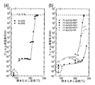
焼き入れされていない複合材料420は、わずかに高い初期σdc≒10−6から10−5 S cm−1を有する。複合材料分散液416のPEDTは、窒素の中で300℃まで耐えることのできる堅牢な導電ポリマーであり、複合材料420のバックグラウンド導電率を設定するσdc≒10−6S cm−1となる。σdcは160℃から200℃で、焼き入れされていない複合材料420の組成に応じて最高10−5から10−3Scm−1まで上昇する。22から23ÅのAuとの70:30v/vの焼き入れされていない複合材料420は、きわめて導電状態に210℃から230℃の間で変態する。複合材料分散液416のPEDTは、焼き入れされていない複合材料420の変態温度を15℃から20℃だけ少しばかり遅らせるようであり、高Au体積分率≒0.7で、小さいAuサイズが33Å以下のフィルムの最終σdcに有害な影響を与えない。これは、焼き入れされていない複合材料420が均質であることを証明している。おそらくポリマーとナノ粒子のOH−終端保護単層とCOOH−終端保護単層の間の好ましい相互作用(水素結合)の結果として固形状態においても相分離は発生せず、ナノ粒子−ポリマー系の共通の特徴である相分離を回避する。さらに大きなナノ粒子の場合、Tpはさらに遅らされ、達成可能なσdcが減少する。さらに大きいAuサイズの焼き入れされていない複合材料418は電子ホッピングレートを減速させる比例的にさらに大きいAu間の間隔を有するので、予想外ではない。(Abeles Bら、Adv Phys、24:406から461、1975年)。これは図6に示されている。
The unquenched
焼き入れされていない複合材料420での金のナノ粒子は、約240℃での表面溶解遷移を示す。焼き入れされていない複合材料420は、閾値温度を横切ると約4x10⁵S cm−1への導電率の1010倍より大きい増加を示す。PEDT:PSSで調製される、焼き入れされていない複合材料420は、95%の金から30%の金の間の範囲となる金とPEDTの異なる体積分率のために240℃から270℃の同じ範囲内の閾値温度も有する。ポリマーの体積分率が増加するにつれ、閾値温度は増加する。40%より大きいまたは40%に等しいポリマー体積分率の場合、バルク連続金属状態は開発できない。
Gold nanoparticles in the
線形電界効果孔の移動性は、リソグラフィーでパターン化されたAuソースドレインアレイの上に製造された対応するデバイスよりわずかに高い4×10⁻⁴cm2V-1s-1であると決定される。これは、ここで説明されている導電性複合材料422が、TFBの中に穴を注入することができ、トランジスタ性能に有害な影響を及ぼさないことを示している。 The mobility of the linear field effect hole is determined to be 4 × 10 −4 cm 2 V −1 s −1 which is slightly higher than the corresponding device fabricated on the lithographically patterned Au source / drain array. The This indicates that the conductive composite 422 described herein can inject holes into the TFB and does not adversely affect transistor performance.
これらの焼き入れされていない複合材料420の絶縁体−金属境界を横切る構造進化は、それらの光学スペクトルから推測できることが判明した。断面TEMによる直接的なイメージングは、ナノAu粒子の多数の密度のために、ここでは可能ではない。ナノ−Auフィルムの、及びAu−ポリマーフィルムの光学透過スペクトルは、それぞれ図7aと図7bに比較のために示されている。Tpの下では、焼き入れされていない複合材料420が、発振器強度で増加し、540nmから575nmに赤方偏移する独特なプラズモンバンドを示す。Tpでは、プラズモン特長は突然、三次元パーコレーション構造の形成を示す、赤外線から近赤外線に伸びるドルーデテールの中に消える。しかしながら、複合材料は、それが650nmでの弱いプラズモン残余の保持によって証明されるように、依然として格子間の空間の中に有機物のかなりの留分を組み込むため、依然としてナノ構造化されており、バルクAuとは異なる。
It has been found that the structural evolution across the insulator-metal interface of these
類似した特徴は、15℃から20℃分のTpの遅延及び最終的な導電性複合材料422における30 v/v%ポリマーの存在を除き、導電性複合材料422でも見られる。これが、増分ステップで絶縁体−金属境界を交差し、変態のさらに詳細なスペクトルを取得することを可能にする。光学分光学から、ドルーデテールの出現は、絶縁体−金属変態が215℃から230℃で発生することを示し、σdcの測定と完全に一致している。光学変換及び電気変換はともに発生する。
Similar features are seen in the
メモリ素子としての応用例
焼き入れされていない複合材料420の変態は、電気的にも誘発されてよい。これがメモリ素子の基本である。変態を達成するために必要とされる電場は、数MV cm−1の範囲内であってよい。この変態は、図8a及び図8bに描かれている。垂直のクロスワイヤセル構造は、複合材料分散液を形成するために1:1のAu(33−Å)−PEDTで製造された。メモリ素子は、単純な三層プロセスで製造された。第1のステップは、厚さが50nmと0.1mmの幅の平行した金の線の蒸発を含んでいた。この層の上には、1:1のAu(33−Å)−PEDT複合材料分散液がスピンコーティングにより付着され、厚さ〜100nmの複合フィルムをもたらす。最終的なステップは、底部層に垂直な方向での金の線の蒸発で、断面積10−4cm2及び〜100cmの厚さを有する各セルまたはメモリ素子のある垂直クロスワイヤセル構造をもたらした。上部電極及び底部電極は、金の代わりに、アルミニウム、銅、または銀のような他の金属であってよい。低電圧では、セルはAu−PEDTの予想された非オームIV特徴及び(σdc≒5×10⁻⁶Scm−1に対応する)20kΩという0Vでの予想抵抗を示す。印加電圧が40Vに達すると、セル抵抗は300Ωまで削減され、IV特長はオーム(10−3Scm−1)になる。絶縁体−金属変態がAu−PEDTの全体的なバルクに行き渡るのではなく、おそらくフィラメント状の経路に制限されることは明らかである。220℃までの焼きなまし(別のセル)時、その抵抗は、熱的に誘導された変態の開始に達した結果、20kΩから650Ω(4x10−4S cm−1)に低下する。以後の電圧掃引の間、Vが25Vに達すると、抵抗はさらに40Ω(10−2S cm−1)に低下する。必要とされる電圧は、現在以前より低くなっている。熱的に誘発される、発生しようとしている導電経路の存在と一致して、これらの経路を完全にパーコレートさせるために必要とされる電場は小さくなる。いったん形成されると、電流伝導経路は安定している。これは、これらの印刷可能複合材料のために考えられる不揮発性メモリ応用例を示唆している。表面的には、これは1971年に遡る誘電体ポリマー薄膜で報告された電気スイッチング挙動に似ている。例えば、複合材料は、電流フィラメント型のメモリ素子に適切であってよい。前記の利点は、必要とされる電場がはるかに小さいという点であり、電流フィラメントはナノ粒子を通過しなければならないため、例えば体積分率及び焼きなまし前のサイズのようなその特性は、必要とされるセルの特徴を調整する手段を提供する。
Application Example as Memory Element The transformation of the unquenched
Claims (4)
保護単層を有し、金(Au)、銀(Ag)、白金(Pt)、パラジウム(Pd)及びその任意の組み合わせ又はそれらの合金から成るグループから選択され、平均直径が1〜20nmである不活性金属ナノ粒子を準備し、
該保護単層材料が、
(a)一方の端部で保護された前記金属ナノ粒子に結合できる基(X)と、他方の端部で溶媒の中で溶媒和できる基(Y)で官能基化されている1つまたは複数のアルキル鎖または芳香族部分を備え、かつ/又は
(b)1つ以上のポリマーの鎖長に沿って該保護された金属ナノ粒子に結合できる基(X)と、溶媒の中で溶媒和できる基(Y)を備える1つ以上のポリマーを備え、
複合材料分散液を形成するために、保護されている該金属ナノ粒子及びポリマーを溶媒中で分散することにより、
前記ポリマーはポリアニオン及びポリカチオンの群より選択される高分子電解質である、複合材料分散液を調製するステップと、
複合フィルムを形成するために該複合材料分散液を基板上に付着させるステップと、
焼き入れされていない複合材料を形成するために該複合フィルムから該溶媒を蒸発させるステップと、
該導電性複合材料を形成するために該焼き入れされていない複合材料を180℃から250℃の温度範囲の間で焼きなますステップと、
を備え、
該焼きなますステップ後の該導電性複合材料の導電率が4インラインプローブ技法を使用して決定され104S cm−1を超え、該焼きなますステップ後の該導電性複合材料は、隣接する前記金属ナノ粒子間のコア−コア癒着に起因する伝達経路を含み、前記ポリマーの体積分率が焼きなます前の該導電性複合材料の20〜80%の間である、
導電性複合材料を調製する方法。 A method of preparing a conductive composite material, comprising:
It has a protective monolayer and is selected from the group consisting of gold (Au), silver (Ag), platinum (Pt), palladium (Pd) and any combination thereof or alloys thereof, and has an average diameter of 1 to 20 nm Prepare inert metal nanoparticles,
The protective monolayer material is
(A) one functionalized with a group (X) that can bind to the metal nanoparticles protected at one end and a group (Y) that can be solvated in a solvent at the other end, or A group (X) comprising a plurality of alkyl chains or aromatic moieties and / or (b) capable of binding to the protected metal nanoparticles along the chain length of one or more polymers, and solvating in a solvent Comprising one or more polymers with possible groups (Y),
By dispersing the protected metal nanoparticles and polymer in a solvent to form a composite dispersion,
Preparing a composite dispersion, wherein the polymer is a polyelectrolyte selected from the group of polyanions and polycations;
Depositing the composite dispersion on a substrate to form a composite film;
Evaporating the solvent from the composite film to form an unquenched composite material;
Annealing the unquenched composite material between a temperature range of 180 ° C. to 250 ° C. to form the conductive composite material;
With
The conductivity of the conductive composite after the annealing step is determined using a 4 in-line probe technique and exceeds 10 4 S cm −1, and the conductive composite after the annealing step is adjacent Including a transmission path resulting from core-core adhesion between the metal nanoparticles, wherein the volume fraction of the polymer is between 20-80% of the conductive composite prior to annealing,
A method of preparing a conductive composite material.
The group (Y) is selected from hydroxyl, amine, ester, amide, acid, ammonium, quaternized ammonium and ethylene glycol, and the group (X) is a thiol group, amine group, phosphine group, isonitrile group, nitrile group, 4. A process according to any one of claims 1 to 3 selected from silane groups, hydroxyl groups and acidic groups.
Applications Claiming Priority (2)
| Application Number | Priority Date | Filing Date | Title |
|---|---|---|---|
| US69592905P | 2005-07-01 | 2005-07-01 | |
| US60/695,929 | 2005-07-01 |
Related Parent Applications (1)
| Application Number | Title | Priority Date | Filing Date |
|---|---|---|---|
| JP2008520015A Division JP5753338B2 (en) | 2005-07-01 | 2006-07-03 | Conductive composite material |
Publications (2)
| Publication Number | Publication Date |
|---|---|
| JP2015122310A JP2015122310A (en) | 2015-07-02 |
| JP5908962B2 true JP5908962B2 (en) | 2016-04-26 |
Family
ID=37604839
Family Applications (2)
| Application Number | Title | Priority Date | Filing Date |
|---|---|---|---|
| JP2008520015A Expired - Fee Related JP5753338B2 (en) | 2005-07-01 | 2006-07-03 | Conductive composite material |
| JP2014243279A Expired - Fee Related JP5908962B2 (en) | 2005-07-01 | 2014-12-01 | Method for preparing conductive composite material |
Family Applications Before (1)
| Application Number | Title | Priority Date | Filing Date |
|---|---|---|---|
| JP2008520015A Expired - Fee Related JP5753338B2 (en) | 2005-07-01 | 2006-07-03 | Conductive composite material |
Country Status (6)
| Country | Link |
|---|---|
| US (1) | US8421231B2 (en) |
| EP (1) | EP1899986B1 (en) |
| JP (2) | JP5753338B2 (en) |
| KR (1) | KR101423204B1 (en) |
| CN (1) | CN101238528B (en) |
| WO (1) | WO2007004033A2 (en) |
Families Citing this family (42)
| Publication number | Priority date | Publication date | Assignee | Title |
|---|---|---|---|---|
| EP2050319A4 (en) | 2006-07-21 | 2010-12-08 | Valtion Teknillinen | Method for manufacturing conductors and semiconductors |
| US7611985B2 (en) * | 2006-09-20 | 2009-11-03 | Intel Corporation | Formation of holes in substrates using dewetting coatings |
| TWI345835B (en) * | 2007-01-02 | 2011-07-21 | Chunghwa Picture Tubes Ltd | Organic thin film transistor and method for manufacturing thereof |
| US10231344B2 (en) | 2007-05-18 | 2019-03-12 | Applied Nanotech Holdings, Inc. | Metallic ink |
| FI122644B (en) | 2007-06-08 | 2012-04-30 | Teknologian Tutkimuskeskus Vtt | Process for forming electrically conductive or semiconducting paths on a substrate and using the method for producing transistors and producing sensors |
| FI122011B (en) | 2007-06-08 | 2011-07-15 | Teknologian Tutkimuskeskus Vtt | Method for Producing an Electronic Module, Intermediate to Produce an Electronic Module, Memory Element, Printed Electronic Product, Sensor Device, and RFID Tag |
| FI122014B (en) | 2007-06-08 | 2011-07-15 | Teknologian Tutkimuskeskus Vtt | Method and apparatus for the functionalization of nanoparticle systems |
| US7768366B1 (en) * | 2007-10-29 | 2010-08-03 | The United States Of America As Represented By The Secretary Of The Air Force | Nanoparticles and corona enhanced MEMS switch apparatus |
| US9730333B2 (en) | 2008-05-15 | 2017-08-08 | Applied Nanotech Holdings, Inc. | Photo-curing process for metallic inks |
| FR2934705B1 (en) * | 2008-07-29 | 2015-10-02 | Univ Toulouse 3 Paul Sabatier | ELECTRICALLY CONDUCTIVE COMPOSITE SOLID MATERIAL AND METHOD FOR OBTAINING SUCH MATERIAL |
| DE112009001984B4 (en) * | 2008-08-11 | 2017-10-12 | Daiken Chemical Co. Ltd. | Composite nanoparticles and manufacturing method therefor |
| JP4477083B2 (en) * | 2008-09-24 | 2010-06-09 | 株式会社東芝 | Method for producing metal nanoparticle inorganic composite, metal nanoparticle inorganic composite, and plasmon waveguide |
| EP2351471A1 (en) * | 2008-09-29 | 2011-08-03 | Nederlandse Organisatie voor toegepast -natuurwetenschappelijk onderzoek TNO | Kit for preparing a conductive pattern |
| JP5243181B2 (en) * | 2008-10-20 | 2013-07-24 | スリーエム イノベイティブ プロパティズ カンパニー | Thermoelectric element using conductive polymer composite and conductive polymer material |
| JP5453789B2 (en) * | 2008-12-04 | 2014-03-26 | 東洋紡株式会社 | Metal fine particle dispersion, method for producing metal thin film, and metal thin film |
| KR101735710B1 (en) | 2009-03-27 | 2017-05-15 | 어플라이드 나노테크 홀딩스, 인크. | Buffer layer to enhance photo and/or laser sintering |
| EP2492351B1 (en) * | 2009-07-30 | 2018-06-06 | Fundacion Cidetec | Electrochemical sensor for the detection of analytes in liquid media |
| FI124372B (en) * | 2009-11-13 | 2014-07-31 | Teknologian Tutkimuskeskus Vtt | Method and products related to the deposited particles |
| US8920681B2 (en) | 2009-12-30 | 2014-12-30 | Korea University Research And Business Foundation | Electrically conductive polymers with enhanced conductivity |
| US8558117B2 (en) * | 2010-02-13 | 2013-10-15 | Aculon, Inc. | Electroconductive inks made with metallic nanoparticles |
| CN102071453B (en) * | 2010-12-14 | 2012-05-02 | 吉林大学 | Method for preparing high-quality aqueous phase semiconductor nanocrystals by one pot method at room temperature |
| WO2012090339A1 (en) * | 2010-12-28 | 2012-07-05 | 東北精機工業株式会社 | Process for production of compound having chalcopyrite structure |
| US8986819B2 (en) * | 2011-06-06 | 2015-03-24 | Xerox Corporation | Palladium precursor composition |
| US20140001420A1 (en) * | 2011-09-30 | 2014-01-02 | Lawrence T. Drzal | Method of preparing metal nanoparticles |
| CN103192086B (en) * | 2012-01-10 | 2015-05-13 | 中国科学院宁波材料技术与工程研究所 | Preparation method for controllable duplex metal alloy nano particle |
| US9598776B2 (en) | 2012-07-09 | 2017-03-21 | Pen Inc. | Photosintering of micron-sized copper particles |
| CN104176701B (en) * | 2014-08-18 | 2016-08-24 | 中国科学院上海应用物理研究所 | The gold nanoparticle film of organic ligand parcel and Field Electron Emission device thereof |
| US9947431B2 (en) * | 2015-04-21 | 2018-04-17 | The Florida International University Board Of Trustees | Anisotropic films templated using ultrasonic focusing |
| CN104861189B (en) * | 2015-05-25 | 2018-04-13 | 华南理工大学 | A kind of method of poly- 3,4 ethylenedioxy thiophenes of fabricated in situ/nanometer metallic silver transparent conducting coating |
| CN105225721B (en) * | 2015-08-26 | 2017-04-19 | 贵州理工学院 | Highly-conductive composite metal oxidation powder material and preparation method thereof |
| FR3042305B1 (en) * | 2015-10-13 | 2019-07-26 | Arkema France | METHOD FOR MANUFACTURING CONDUCTIVE COMPOSITE MATERIAL AND COMPOSITE MATERIAL THUS OBTAINED |
| US20190100663A1 (en) * | 2017-10-03 | 2019-04-04 | Shin-Etsu Chemical Co., Ltd. | Anisotropic conductive film and method for manufacturing anisotropic conductive film |
| KR102578825B1 (en) | 2017-10-31 | 2023-09-15 | 삼성전자주식회사 | Conductive composite structure for electronic device, preparaing method thereof, electrode for electronic device including the same, and electronic devices comprising the same |
| EP3804886A4 (en) * | 2018-06-08 | 2022-02-09 | Korea Institute of Science and Technology | Micro-nanostructure manufactured using amorphous nanostructure and manufacturing method therefor |
| KR102432090B1 (en) * | 2018-06-08 | 2022-08-12 | 한국과학기술연구원 | Ultrasmall Nanostructure formed by using Amorphous Nanostructure and Method of manufacturing the same |
| KR102102185B1 (en) * | 2018-10-05 | 2020-04-21 | 한국과학기술연구원 | Conducting polymer composite with high strechability |
| KR102102186B1 (en) * | 2018-10-05 | 2020-04-21 | 한국과학기술연구원 | Conducting polymer composite with high strechability and method for manufacturing the same |
| KR102608512B1 (en) * | 2019-02-19 | 2023-11-30 | 엘에스전선 주식회사 | Superconducting Cable And Manufacturing Method Of The Same |
| WO2020230162A1 (en) * | 2019-05-12 | 2020-11-19 | Indian Institute Of Science | Low resistance nanostructured electrical conductor |
| JP6781437B1 (en) * | 2019-07-19 | 2020-11-04 | 株式会社Gceインスティチュート | Power generation element and manufacturing method of power generation element |
| US20210107810A1 (en) * | 2019-10-14 | 2021-04-15 | Quinton Wyatt | Electrically conductive polymer thin-films |
| CN111687428B (en) * | 2020-05-13 | 2021-11-19 | 华南理工大学 | Amphiphilic polymer mediated gold nanoparticle controllable assembly and preparation and application thereof |
Family Cites Families (28)
| Publication number | Priority date | Publication date | Assignee | Title |
|---|---|---|---|---|
| GB8909011D0 (en) | 1989-04-20 | 1989-06-07 | Friend Richard H | Electroluminescent devices |
| JPH05105828A (en) * | 1991-10-16 | 1993-04-27 | Matsushita Electric Works Ltd | Conductive paste |
| JPH05347106A (en) * | 1992-06-16 | 1993-12-27 | Matsushita Electric Ind Co Ltd | Conductive paint |
| US5523555A (en) * | 1994-09-14 | 1996-06-04 | Cambridge Display Technology | Photodetector device having a semiconductive conjugated polymer |
| GB9423692D0 (en) | 1994-11-23 | 1995-01-11 | Philips Electronics Uk Ltd | A photoresponsive device |
| WO1997024224A1 (en) * | 1995-12-28 | 1997-07-10 | Heath James R | Organically-functionalized monodisperse nanocrystals of metals |
| US5973050A (en) * | 1996-07-01 | 1999-10-26 | Integrated Cryoelectronic Inc. | Composite thermoelectric material |
| US6103868A (en) * | 1996-12-27 | 2000-08-15 | The Regents Of The University Of California | Organically-functionalized monodisperse nanocrystals of metals |
| US6251303B1 (en) * | 1998-09-18 | 2001-06-26 | Massachusetts Institute Of Technology | Water-soluble fluorescent nanocrystals |
| EP1146149A4 (en) * | 1999-11-01 | 2006-08-30 | Jsr Corp | Aqueous dispersion for forming conductive layer, conductive layer, electronic component, circuit board and method for manufacturing the same, and multilayer wiring board and method for manufacturing the same |
| GB0006050D0 (en) * | 2000-03-14 | 2000-05-03 | Johnson Matthey Plc | Liquid gold compositions |
| AU2001249459A1 (en) * | 2000-03-24 | 2001-10-08 | The State Of Oregon, Acting By And Through The State Board Of Higher Education On Behalf Of The University Of Oregon | Scaffold-organized clusters and electronic devices made using such clusters |
| KR100857473B1 (en) * | 2000-03-27 | 2008-09-08 | 마이클 에프 레이 | Method of cyanide salt production |
| JP2001325831A (en) * | 2000-05-12 | 2001-11-22 | Bando Chem Ind Ltd | Metal colloid solution, conductive ink, conductive coating and conductive coating forming base film |
| WO2002018080A1 (en) * | 2000-08-03 | 2002-03-07 | Upepo & Maji Inc. | Metal colloidal solution composition and conductor or ink for forming semiconductor pattern comprising it and method for forming conductor or semiconductor pattern |
| US6773926B1 (en) * | 2000-09-25 | 2004-08-10 | California Institute Of Technology | Nanoparticle-based sensors for detecting analytes in fluids |
| US6649138B2 (en) * | 2000-10-13 | 2003-11-18 | Quantum Dot Corporation | Surface-modified semiconductive and metallic nanoparticles having enhanced dispersibility in aqueous media |
| KR100647238B1 (en) * | 2000-10-25 | 2006-11-17 | 하리마카세이 가부시기가이샤 | Electroconductive metal paste and method for production thereof |
| CN1151512C (en) * | 2000-11-23 | 2004-05-26 | 大连三科科技发展有限公司 | Electrically conducting nano-class sb-contained microparticles and preparing process thereof |
| KR100379250B1 (en) * | 2000-12-04 | 2003-04-08 | 한국과학기술연구원 | Composite Polymers Containing Nanometer-sized Metal Particles and Fabrication Method Thereof |
| EP1223615A1 (en) * | 2001-01-10 | 2002-07-17 | Eidgenössische Technische Hochschule Zürich | A method for producing a structure using nanoparticles |
| JP3774638B2 (en) * | 2001-04-24 | 2006-05-17 | ハリマ化成株式会社 | Circuit pattern forming method using inkjet printing method |
| GB0126236D0 (en) * | 2001-11-01 | 2002-01-02 | Univ East Anglia | Photosensitiser functionalised nanoparticles |
| CA2465124A1 (en) * | 2001-11-01 | 2003-05-08 | Yissum Research Development Company Of The Hebrew University In Jerusalem | Ink-jet inks containing metal nanoparticles |
| US7413770B2 (en) * | 2002-08-01 | 2008-08-19 | E.I. Du Pont De Nemours And Company | Ethylene glycol monolayer protected nanoparticles |
| CN100540628C (en) * | 2002-09-24 | 2009-09-16 | E.I.内穆尔杜邦公司 | Conductive organic polymer/nanoparticle composition and application method thereof |
| KR100965373B1 (en) | 2003-06-10 | 2010-06-22 | 삼성전자주식회사 | Photosensitive Metal Nanoparticle and Method of forming Conductive Pattern by using the same |
| EP1666175B1 (en) | 2003-09-12 | 2019-05-15 | SIJTechnology, Inc. | Metal nano particle liquid dispersion capable of being sprayed in fine particle form and being applied in laminated state |
-
2006
- 2006-07-03 US US11/988,183 patent/US8421231B2/en active Active
- 2006-07-03 WO PCT/IB2006/001829 patent/WO2007004033A2/en active Application Filing
- 2006-07-03 JP JP2008520015A patent/JP5753338B2/en not_active Expired - Fee Related
- 2006-07-03 CN CN2006800269399A patent/CN101238528B/en active Active
- 2006-07-03 KR KR1020087001943A patent/KR101423204B1/en not_active IP Right Cessation
- 2006-07-03 EP EP06779815.7A patent/EP1899986B1/en not_active Not-in-force
-
2014
- 2014-12-01 JP JP2014243279A patent/JP5908962B2/en not_active Expired - Fee Related
Also Published As
| Publication number | Publication date |
|---|---|
| KR101423204B1 (en) | 2014-07-25 |
| WO2007004033A3 (en) | 2007-03-29 |
| KR20080034439A (en) | 2008-04-21 |
| JP5753338B2 (en) | 2015-07-22 |
| JP2015122310A (en) | 2015-07-02 |
| US20080265414A1 (en) | 2008-10-30 |
| JP2009500802A (en) | 2009-01-08 |
| CN101238528A (en) | 2008-08-06 |
| EP1899986A4 (en) | 2009-08-12 |
| US8421231B2 (en) | 2013-04-16 |
| EP1899986A2 (en) | 2008-03-19 |
| CN101238528B (en) | 2011-12-07 |
| EP1899986B1 (en) | 2014-05-07 |
| WO2007004033A2 (en) | 2007-01-11 |
Similar Documents
| Publication | Publication Date | Title |
|---|---|---|
| JP5908962B2 (en) | Method for preparing conductive composite material | |
| JP2009500802A5 (en) | ||
| US10403414B2 (en) | Conductive nanowire films | |
| US10237974B2 (en) | Metal nanowire thin-films | |
| Sivaramakrishnan et al. | Controlled insulator-to-metal transformation in printable polymer composites with nanometal clusters | |
| JP5957630B2 (en) | Metal ink | |
| Park et al. | Nanoscale patterning and electronics on flexible substrate by direct nanoimprinting of metallic nanoparticles | |
| US8026185B2 (en) | Method for manufacturing electronic circuit component | |
| US20060163744A1 (en) | Printable electrical conductors | |
| WO2007061428A2 (en) | Components and devices formed using nanoscale materials and methods of production | |
| MX2012010130A (en) | Method of making a coated article, coating including an alloyed carbon nanotube thin film. | |
| Chen et al. | Hybrid printing metal-mesh transparent conductive films with lower energy photonically sintered copper/tin ink | |
| Yu et al. | Morphology, Electrical, and Rheological Properties of Silane‐Modified Silver Nanowire/Polymer Composites | |
| US9418769B2 (en) | Conductive carbon nanotube-metal composite ink | |
| Howell et al. | Mass-fabricated one-dimensional silicon nanogaps for hybrid organic/nanoparticle arrays | |
| JP2019036628A (en) | Capacitor and manufacturing method thereof | |
| CN101908388B (en) | Forming method of nano-dotted materials | |
| Huang et al. | Using soft lithography to fabricate gold nanoparticle patterns for bottom-gate field effect transistors | |
| US20190166699A1 (en) | Printing of nanowire films | |
| Wu et al. | Development of silver nanoparticle ink for printed electronics | |
| Yin et al. | Processing and electrical properties of sodium citrate capped silver nanoparticle based inks for flexible electronics | |
| JP2019212823A (en) | Thermoelectric element and manufacturing method therefor | |
| JP2018003068A (en) | Manufacturing method of metal nanoparticle sintered film | |
| Anto | Nanometal inks for plastic electronics applications | |
| SIVARAMAKRISHNAN | Nanometal conductive layers and organic heterostructures for polymer semiconductor devices |
Legal Events
| Date | Code | Title | Description |
|---|---|---|---|
| A977 | Report on retrieval |
Free format text: JAPANESE INTERMEDIATE CODE: A971007 Effective date: 20150930 |
|
| A131 | Notification of reasons for refusal |
Free format text: JAPANESE INTERMEDIATE CODE: A131 Effective date: 20151104 |
|
| A521 | Request for written amendment filed |
Free format text: JAPANESE INTERMEDIATE CODE: A523 Effective date: 20160204 |
|
| TRDD | Decision of grant or rejection written | ||
| A01 | Written decision to grant a patent or to grant a registration (utility model) |
Free format text: JAPANESE INTERMEDIATE CODE: A01 Effective date: 20160301 |
|
| A61 | First payment of annual fees (during grant procedure) |
Free format text: JAPANESE INTERMEDIATE CODE: A61 Effective date: 20160324 |
|
| R150 | Certificate of patent or registration of utility model |
Ref document number: 5908962 Country of ref document: JP Free format text: JAPANESE INTERMEDIATE CODE: R150 |
|
| LAPS | Cancellation because of no payment of annual fees |