JP5858517B2 - Manufacturing method of organic device - Google Patents
Manufacturing method of organic device Download PDFInfo
- Publication number
- JP5858517B2 JP5858517B2 JP2011160823A JP2011160823A JP5858517B2 JP 5858517 B2 JP5858517 B2 JP 5858517B2 JP 2011160823 A JP2011160823 A JP 2011160823A JP 2011160823 A JP2011160823 A JP 2011160823A JP 5858517 B2 JP5858517 B2 JP 5858517B2
- Authority
- JP
- Japan
- Prior art keywords
- organic
- layer
- solvent
- group
- transfer member
- Prior art date
- Legal status (The legal status is an assumption and is not a legal conclusion. Google has not performed a legal analysis and makes no representation as to the accuracy of the status listed.)
- Expired - Fee Related
Links
- 238000004519 manufacturing process Methods 0.000 title claims description 16
- 239000010410 layer Substances 0.000 claims description 248
- 239000012044 organic layer Substances 0.000 claims description 126
- 239000000463 material Substances 0.000 claims description 110
- 238000000576 coating method Methods 0.000 claims description 81
- 239000011248 coating agent Substances 0.000 claims description 75
- 239000002904 solvent Substances 0.000 claims description 69
- 229920001296 polysiloxane Polymers 0.000 claims description 33
- 239000011368 organic material Substances 0.000 claims description 28
- XLYOFNOQVPJJNP-UHFFFAOYSA-N water Substances O XLYOFNOQVPJJNP-UHFFFAOYSA-N 0.000 claims description 28
- 238000009835 boiling Methods 0.000 claims description 19
- 239000007788 liquid Substances 0.000 claims description 13
- 238000000034 method Methods 0.000 description 61
- 230000032258 transport Effects 0.000 description 50
- -1 and the like Inorganic materials 0.000 description 46
- 238000010438 heat treatment Methods 0.000 description 38
- 239000000203 mixture Substances 0.000 description 37
- VYPSYNLAJGMNEJ-UHFFFAOYSA-N Silicium dioxide Chemical compound O=[Si]=O VYPSYNLAJGMNEJ-UHFFFAOYSA-N 0.000 description 35
- 238000002347 injection Methods 0.000 description 35
- 239000007924 injection Substances 0.000 description 35
- 230000005525 hole transport Effects 0.000 description 31
- 239000000243 solution Substances 0.000 description 31
- CSCPPACGZOOCGX-UHFFFAOYSA-N Acetone Chemical compound CC(C)=O CSCPPACGZOOCGX-UHFFFAOYSA-N 0.000 description 30
- 239000000758 substrate Substances 0.000 description 28
- 239000002585 base Substances 0.000 description 27
- 239000012046 mixed solvent Substances 0.000 description 22
- 239000008119 colloidal silica Substances 0.000 description 20
- 150000001875 compounds Chemical class 0.000 description 19
- 238000003825 pressing Methods 0.000 description 17
- HEDRZPFGACZZDS-UHFFFAOYSA-N Chloroform Chemical compound ClC(Cl)Cl HEDRZPFGACZZDS-UHFFFAOYSA-N 0.000 description 16
- YMWUJEATGCHHMB-UHFFFAOYSA-N dichloromethane Substances ClCCl YMWUJEATGCHHMB-UHFFFAOYSA-N 0.000 description 16
- 150000002430 hydrocarbons Chemical group 0.000 description 16
- YXFVVABEGXRONW-UHFFFAOYSA-N Toluene Chemical compound CC1=CC=CC=C1 YXFVVABEGXRONW-UHFFFAOYSA-N 0.000 description 15
- CERQOIWHTDAKMF-UHFFFAOYSA-N Methacrylic acid Chemical compound CC(=C)C(O)=O CERQOIWHTDAKMF-UHFFFAOYSA-N 0.000 description 13
- 239000012299 nitrogen atmosphere Substances 0.000 description 13
- 239000004925 Acrylic resin Substances 0.000 description 12
- 229920000178 Acrylic resin Polymers 0.000 description 12
- 229910052751 metal Inorganic materials 0.000 description 12
- 239000002184 metal Substances 0.000 description 12
- 239000003960 organic solvent Substances 0.000 description 12
- 230000015572 biosynthetic process Effects 0.000 description 11
- UXJDSNKBYFJNDO-UHFFFAOYSA-N 9-[4-[2-[2-(4-carbazol-9-ylphenyl)phenyl]phenyl]phenyl]carbazole Chemical group C12=CC=CC=C2C2=CC=CC=C2N1C(C=C1)=CC=C1C1=CC=CC=C1C1=CC=CC=C1C1=CC=C(N2C3=CC=CC=C3C3=CC=CC=C32)C=C1 UXJDSNKBYFJNDO-UHFFFAOYSA-N 0.000 description 10
- LFQSCWFLJHTTHZ-UHFFFAOYSA-N Ethanol Chemical compound CCO LFQSCWFLJHTTHZ-UHFFFAOYSA-N 0.000 description 10
- VEXZGXHMUGYJMC-UHFFFAOYSA-N Hydrochloric acid Chemical compound Cl VEXZGXHMUGYJMC-UHFFFAOYSA-N 0.000 description 10
- 238000001035 drying Methods 0.000 description 10
- 150000001282 organosilanes Chemical class 0.000 description 10
- ZWEHNKRNPOVVGH-UHFFFAOYSA-N 2-Butanone Chemical compound CCC(C)=O ZWEHNKRNPOVVGH-UHFFFAOYSA-N 0.000 description 9
- XEKOWRVHYACXOJ-UHFFFAOYSA-N Ethyl acetate Chemical compound CCOC(C)=O XEKOWRVHYACXOJ-UHFFFAOYSA-N 0.000 description 9
- KFZMGEQAYNKOFK-UHFFFAOYSA-N Isopropanol Chemical compound CC(C)O KFZMGEQAYNKOFK-UHFFFAOYSA-N 0.000 description 9
- 125000004432 carbon atom Chemical group C* 0.000 description 8
- MTHSVFCYNBDYFN-UHFFFAOYSA-N diethylene glycol Chemical class OCCOCCO MTHSVFCYNBDYFN-UHFFFAOYSA-N 0.000 description 8
- 238000005401 electroluminescence Methods 0.000 description 8
- LYCAIKOWRPUZTN-UHFFFAOYSA-N Ethylene glycol Chemical compound OCCO LYCAIKOWRPUZTN-UHFFFAOYSA-N 0.000 description 7
- 239000003054 catalyst Substances 0.000 description 7
- 238000006460 hydrolysis reaction Methods 0.000 description 7
- 238000002156 mixing Methods 0.000 description 7
- 125000005372 silanol group Chemical group 0.000 description 7
- 239000000377 silicon dioxide Substances 0.000 description 7
- VFUDMQLBKNMONU-UHFFFAOYSA-N 9-[4-(4-carbazol-9-ylphenyl)phenyl]carbazole Chemical group C12=CC=CC=C2C2=CC=CC=C2N1C1=CC=C(C=2C=CC(=CC=2)N2C3=CC=CC=C3C3=CC=CC=C32)C=C1 VFUDMQLBKNMONU-UHFFFAOYSA-N 0.000 description 6
- QTBSBXVTEAMEQO-UHFFFAOYSA-N Acetic acid Chemical compound CC(O)=O QTBSBXVTEAMEQO-UHFFFAOYSA-N 0.000 description 6
- 150000002009 diols Chemical class 0.000 description 6
- YERGTYJYQCLVDM-UHFFFAOYSA-N iridium(3+);2-(4-methylphenyl)pyridine Chemical compound [Ir+3].C1=CC(C)=CC=C1C1=CC=CC=N1.C1=CC(C)=CC=C1C1=CC=CC=N1.C1=CC(C)=CC=C1C1=CC=CC=N1 YERGTYJYQCLVDM-UHFFFAOYSA-N 0.000 description 6
- 238000002360 preparation method Methods 0.000 description 6
- 239000011347 resin Substances 0.000 description 6
- 229920005989 resin Polymers 0.000 description 6
- 238000002834 transmittance Methods 0.000 description 6
- 125000000217 alkyl group Chemical group 0.000 description 5
- 238000006482 condensation reaction Methods 0.000 description 5
- 125000002496 methyl group Chemical group [H]C([H])([H])* 0.000 description 5
- 125000001997 phenyl group Chemical group [H]C1=C([H])C([H])=C(*)C([H])=C1[H] 0.000 description 5
- 239000007787 solid Substances 0.000 description 5
- 238000001771 vacuum deposition Methods 0.000 description 5
- YLQBMQCUIZJEEH-UHFFFAOYSA-N Furan Chemical compound C=1C=COC=1 YLQBMQCUIZJEEH-UHFFFAOYSA-N 0.000 description 4
- LRHPLDYGYMQRHN-UHFFFAOYSA-N N-Butanol Chemical compound CCCCO LRHPLDYGYMQRHN-UHFFFAOYSA-N 0.000 description 4
- WYURNTSHIVDZCO-UHFFFAOYSA-N Tetrahydrofuran Chemical compound C1CCOC1 WYURNTSHIVDZCO-UHFFFAOYSA-N 0.000 description 4
- 125000003545 alkoxy group Chemical group 0.000 description 4
- 229910052782 aluminium Inorganic materials 0.000 description 4
- 150000001716 carbazoles Chemical class 0.000 description 4
- 239000010406 cathode material Substances 0.000 description 4
- 238000006243 chemical reaction Methods 0.000 description 4
- 229920001577 copolymer Polymers 0.000 description 4
- 238000000151 deposition Methods 0.000 description 4
- SWXVUIWOUIDPGS-UHFFFAOYSA-N diacetone alcohol Chemical compound CC(=O)CC(C)(C)O SWXVUIWOUIDPGS-UHFFFAOYSA-N 0.000 description 4
- 230000000694 effects Effects 0.000 description 4
- 230000007062 hydrolysis Effects 0.000 description 4
- ZXEKIIBDNHEJCQ-UHFFFAOYSA-N isobutanol Chemical compound CC(C)CO ZXEKIIBDNHEJCQ-UHFFFAOYSA-N 0.000 description 4
- PQXKHYXIUOZZFA-UHFFFAOYSA-M lithium fluoride Chemical compound [Li+].[F-] PQXKHYXIUOZZFA-UHFFFAOYSA-M 0.000 description 4
- BFXIKLCIZHOAAZ-UHFFFAOYSA-N methyltrimethoxysilane Chemical compound CO[Si](C)(OC)OC BFXIKLCIZHOAAZ-UHFFFAOYSA-N 0.000 description 4
- IBHBKWKFFTZAHE-UHFFFAOYSA-N n-[4-[4-(n-naphthalen-1-ylanilino)phenyl]phenyl]-n-phenylnaphthalen-1-amine Chemical group C1=CC=CC=C1N(C=1C2=CC=CC=C2C=CC=1)C1=CC=C(C=2C=CC(=CC=2)N(C=2C=CC=CC=2)C=2C3=CC=CC=C3C=CC=2)C=C1 IBHBKWKFFTZAHE-UHFFFAOYSA-N 0.000 description 4
- 229910052757 nitrogen Inorganic materials 0.000 description 4
- 239000002985 plastic film Substances 0.000 description 4
- 238000004544 sputter deposition Methods 0.000 description 4
- 125000005259 triarylamine group Chemical group 0.000 description 4
- 238000007740 vapor deposition Methods 0.000 description 4
- YCKRFDGAMUMZLT-UHFFFAOYSA-N Fluorine atom Chemical compound [F] YCKRFDGAMUMZLT-UHFFFAOYSA-N 0.000 description 3
- OKKJLVBELUTLKV-UHFFFAOYSA-N Methanol Chemical compound OC OKKJLVBELUTLKV-UHFFFAOYSA-N 0.000 description 3
- MUBZPKHOEPUJKR-UHFFFAOYSA-N Oxalic acid Chemical compound OC(=O)C(O)=O MUBZPKHOEPUJKR-UHFFFAOYSA-N 0.000 description 3
- 239000004793 Polystyrene Substances 0.000 description 3
- KWYUFKZDYYNOTN-UHFFFAOYSA-M Potassium hydroxide Chemical compound [OH-].[K+] KWYUFKZDYYNOTN-UHFFFAOYSA-M 0.000 description 3
- OFOBLEOULBTSOW-UHFFFAOYSA-N Propanedioic acid Natural products OC(=O)CC(O)=O OFOBLEOULBTSOW-UHFFFAOYSA-N 0.000 description 3
- 239000007983 Tris buffer Substances 0.000 description 3
- XLOMVQKBTHCTTD-UHFFFAOYSA-N Zinc monoxide Chemical compound [Zn]=O XLOMVQKBTHCTTD-UHFFFAOYSA-N 0.000 description 3
- 229910052783 alkali metal Inorganic materials 0.000 description 3
- 229910001508 alkali metal halide Inorganic materials 0.000 description 3
- 150000008045 alkali metal halides Chemical class 0.000 description 3
- 229910000272 alkali metal oxide Inorganic materials 0.000 description 3
- 150000001340 alkali metals Chemical class 0.000 description 3
- 229910052784 alkaline earth metal Inorganic materials 0.000 description 3
- 150000001342 alkaline earth metals Chemical class 0.000 description 3
- 125000005370 alkoxysilyl group Chemical group 0.000 description 3
- 229910045601 alloy Inorganic materials 0.000 description 3
- 239000000956 alloy Substances 0.000 description 3
- XAGFODPZIPBFFR-UHFFFAOYSA-N aluminium Chemical compound [Al] XAGFODPZIPBFFR-UHFFFAOYSA-N 0.000 description 3
- KRKNYBCHXYNGOX-UHFFFAOYSA-N citric acid Chemical compound OC(=O)CC(O)(C(O)=O)CC(O)=O KRKNYBCHXYNGOX-UHFFFAOYSA-N 0.000 description 3
- 125000003983 fluorenyl group Chemical class C1(=CC=CC=2C3=CC=CC=C3CC12)* 0.000 description 3
- 229910052731 fluorine Inorganic materials 0.000 description 3
- 239000011737 fluorine Substances 0.000 description 3
- 125000002887 hydroxy group Chemical group [H]O* 0.000 description 3
- VLKZOEOYAKHREP-UHFFFAOYSA-N n-Hexane Chemical compound CCCCCC VLKZOEOYAKHREP-UHFFFAOYSA-N 0.000 description 3
- 229920002223 polystyrene Polymers 0.000 description 3
- 230000008569 process Effects 0.000 description 3
- 239000004447 silicone coating Substances 0.000 description 3
- 125000003808 silyl group Chemical group [H][Si]([H])([H])[*] 0.000 description 3
- 239000002356 single layer Substances 0.000 description 3
- POAOYUHQDCAZBD-UHFFFAOYSA-N 2-butoxyethanol Chemical compound CCCCOCCO POAOYUHQDCAZBD-UHFFFAOYSA-N 0.000 description 2
- ZNQVEEAIQZEUHB-UHFFFAOYSA-N 2-ethoxyethanol Chemical compound CCOCCO ZNQVEEAIQZEUHB-UHFFFAOYSA-N 0.000 description 2
- 125000000094 2-phenylethyl group Chemical group [H]C1=C([H])C([H])=C(C([H])=C1[H])C([H])([H])C([H])([H])* 0.000 description 2
- 125000006201 3-phenylpropyl group Chemical group [H]C1=C([H])C([H])=C(C([H])=C1[H])C([H])([H])C([H])([H])C([H])([H])* 0.000 description 2
- LTUJKAYZIMMJEP-UHFFFAOYSA-N 9-[4-(4-carbazol-9-yl-2-methylphenyl)-3-methylphenyl]carbazole Chemical group C12=CC=CC=C2C2=CC=CC=C2N1C1=CC=C(C=2C(=CC(=CC=2)N2C3=CC=CC=C3C3=CC=CC=C32)C)C(C)=C1 LTUJKAYZIMMJEP-UHFFFAOYSA-N 0.000 description 2
- QGZKDVFQNNGYKY-UHFFFAOYSA-N Ammonia Chemical compound N QGZKDVFQNNGYKY-UHFFFAOYSA-N 0.000 description 2
- DKPFZGUDAPQIHT-UHFFFAOYSA-N Butyl acetate Natural products CCCCOC(C)=O DKPFZGUDAPQIHT-UHFFFAOYSA-N 0.000 description 2
- 239000004593 Epoxy Substances 0.000 description 2
- AEMRFAOFKBGASW-UHFFFAOYSA-N Glycolic acid Chemical compound OCC(O)=O AEMRFAOFKBGASW-UHFFFAOYSA-N 0.000 description 2
- 101000653679 Homo sapiens Translationally-controlled tumor protein Proteins 0.000 description 2
- DGAQECJNVWCQMB-PUAWFVPOSA-M Ilexoside XXIX Chemical compound C[C@@H]1CC[C@@]2(CC[C@@]3(C(=CC[C@H]4[C@]3(CC[C@@H]5[C@@]4(CC[C@@H](C5(C)C)OS(=O)(=O)[O-])C)C)[C@@H]2[C@]1(C)O)C)C(=O)O[C@H]6[C@@H]([C@H]([C@@H]([C@H](O6)CO)O)O)O.[Na+] DGAQECJNVWCQMB-PUAWFVPOSA-M 0.000 description 2
- WHXSMMKQMYFTQS-UHFFFAOYSA-N Lithium Chemical compound [Li] WHXSMMKQMYFTQS-UHFFFAOYSA-N 0.000 description 2
- NTIZESTWPVYFNL-UHFFFAOYSA-N Methyl isobutyl ketone Chemical compound CC(C)CC(C)=O NTIZESTWPVYFNL-UHFFFAOYSA-N 0.000 description 2
- UIHCLUNTQKBZGK-UHFFFAOYSA-N Methyl isobutyl ketone Natural products CCC(C)C(C)=O UIHCLUNTQKBZGK-UHFFFAOYSA-N 0.000 description 2
- IMNFDUFMRHMDMM-UHFFFAOYSA-N N-Heptane Chemical compound CCCCCCC IMNFDUFMRHMDMM-UHFFFAOYSA-N 0.000 description 2
- ZBZXYUYUUDZCNB-UHFFFAOYSA-N N-cyclohexa-1,3-dien-1-yl-N-phenyl-4-[4-(N-[4-[4-(N-[4-[4-(N-phenylanilino)phenyl]phenyl]anilino)phenyl]phenyl]anilino)phenyl]aniline Chemical compound C1=CCCC(N(C=2C=CC=CC=2)C=2C=CC(=CC=2)C=2C=CC(=CC=2)N(C=2C=CC=CC=2)C=2C=CC(=CC=2)C=2C=CC(=CC=2)N(C=2C=CC=CC=2)C=2C=CC(=CC=2)C=2C=CC(=CC=2)N(C=2C=CC=CC=2)C=2C=CC=CC=2)=C1 ZBZXYUYUUDZCNB-UHFFFAOYSA-N 0.000 description 2
- CTQNGGLPUBDAKN-UHFFFAOYSA-N O-Xylene Chemical compound CC1=CC=CC=C1C CTQNGGLPUBDAKN-UHFFFAOYSA-N 0.000 description 2
- 229920001609 Poly(3,4-ethylenedioxythiophene) Polymers 0.000 description 2
- 239000004952 Polyamide Substances 0.000 description 2
- 239000006087 Silane Coupling Agent Substances 0.000 description 2
- 102100029887 Translationally-controlled tumor protein Human genes 0.000 description 2
- 229920006243 acrylic copolymer Polymers 0.000 description 2
- 239000010405 anode material Substances 0.000 description 2
- 125000003710 aryl alkyl group Chemical group 0.000 description 2
- 125000003118 aryl group Chemical group 0.000 description 2
- 239000012298 atmosphere Substances 0.000 description 2
- QVGXLLKOCUKJST-UHFFFAOYSA-N atomic oxygen Chemical compound [O] QVGXLLKOCUKJST-UHFFFAOYSA-N 0.000 description 2
- WPYMKLBDIGXBTP-UHFFFAOYSA-N benzoic acid Chemical compound OC(=O)C1=CC=CC=C1 WPYMKLBDIGXBTP-UHFFFAOYSA-N 0.000 description 2
- 230000000903 blocking effect Effects 0.000 description 2
- 239000003795 chemical substances by application Substances 0.000 description 2
- MVPPADPHJFYWMZ-UHFFFAOYSA-N chlorobenzene Chemical compound ClC1=CC=CC=C1 MVPPADPHJFYWMZ-UHFFFAOYSA-N 0.000 description 2
- 125000004218 chloromethyl group Chemical group [H]C([H])(Cl)* 0.000 description 2
- 229920001940 conductive polymer Polymers 0.000 description 2
- 125000000753 cycloalkyl group Chemical group 0.000 description 2
- 125000000113 cyclohexyl group Chemical group [H]C1([H])C([H])([H])C([H])([H])C([H])(*)C([H])([H])C1([H])[H] 0.000 description 2
- 125000001511 cyclopentyl group Chemical group [H]C1([H])C([H])([H])C([H])([H])C([H])(*)C1([H])[H] 0.000 description 2
- 230000007423 decrease Effects 0.000 description 2
- 229940028356 diethylene glycol monobutyl ether Drugs 0.000 description 2
- LIKFHECYJZWXFJ-UHFFFAOYSA-N dimethyldichlorosilane Chemical compound C[Si](C)(Cl)Cl LIKFHECYJZWXFJ-UHFFFAOYSA-N 0.000 description 2
- XBDQKXXYIPTUBI-UHFFFAOYSA-N dimethylselenoniopropionate Natural products CCC(O)=O XBDQKXXYIPTUBI-UHFFFAOYSA-N 0.000 description 2
- 239000002019 doping agent Substances 0.000 description 2
- 125000003700 epoxy group Chemical group 0.000 description 2
- 125000001495 ethyl group Chemical group [H]C([H])([H])C([H])([H])* 0.000 description 2
- 230000002349 favourable effect Effects 0.000 description 2
- NIHNNTQXNPWCJQ-UHFFFAOYSA-N fluorene Chemical compound C1=CC=C2CC3=CC=CC=C3C2=C1 NIHNNTQXNPWCJQ-UHFFFAOYSA-N 0.000 description 2
- 239000011888 foil Substances 0.000 description 2
- 150000002240 furans Chemical class 0.000 description 2
- 239000011521 glass Substances 0.000 description 2
- 125000003055 glycidyl group Chemical group C(C1CO1)* 0.000 description 2
- PCHJSUWPFVWCPO-UHFFFAOYSA-N gold Chemical compound [Au] PCHJSUWPFVWCPO-UHFFFAOYSA-N 0.000 description 2
- 229910052737 gold Inorganic materials 0.000 description 2
- 239000010931 gold Substances 0.000 description 2
- 125000003187 heptyl group Chemical group [H]C([*])([H])C([H])([H])C([H])([H])C([H])([H])C([H])([H])C([H])([H])C([H])([H])[H] 0.000 description 2
- 125000000623 heterocyclic group Chemical group 0.000 description 2
- FUZZWVXGSFPDMH-UHFFFAOYSA-M hexanoate Chemical compound CCCCCC([O-])=O FUZZWVXGSFPDMH-UHFFFAOYSA-M 0.000 description 2
- 125000004051 hexyl group Chemical group [H]C([H])([H])C([H])([H])C([H])([H])C([H])([H])C([H])([H])C([H])([H])* 0.000 description 2
- 230000003301 hydrolyzing effect Effects 0.000 description 2
- UEEXRMUCXBPYOV-UHFFFAOYSA-N iridium;2-phenylpyridine Chemical compound [Ir].C1=CC=CC=C1C1=CC=CC=N1.C1=CC=CC=C1C1=CC=CC=N1.C1=CC=CC=C1C1=CC=CC=N1 UEEXRMUCXBPYOV-UHFFFAOYSA-N 0.000 description 2
- 125000001449 isopropyl group Chemical group [H]C([H])([H])C([H])(*)C([H])([H])[H] 0.000 description 2
- 238000010030 laminating Methods 0.000 description 2
- 229910052744 lithium Inorganic materials 0.000 description 2
- 230000007774 longterm Effects 0.000 description 2
- 150000002739 metals Chemical class 0.000 description 2
- BDAGIHXWWSANSR-UHFFFAOYSA-N methanoic acid Natural products OC=O BDAGIHXWWSANSR-UHFFFAOYSA-N 0.000 description 2
- 239000005055 methyl trichlorosilane Substances 0.000 description 2
- HLXDKGBELJJMHR-UHFFFAOYSA-N methyl-tri(propan-2-yloxy)silane Chemical compound CC(C)O[Si](C)(OC(C)C)OC(C)C HLXDKGBELJJMHR-UHFFFAOYSA-N 0.000 description 2
- JLUFWMXJHAVVNN-UHFFFAOYSA-N methyltrichlorosilane Chemical compound C[Si](Cl)(Cl)Cl JLUFWMXJHAVVNN-UHFFFAOYSA-N 0.000 description 2
- WHIVNJATOVLWBW-UHFFFAOYSA-N n-butan-2-ylidenehydroxylamine Chemical compound CCC(C)=NO WHIVNJATOVLWBW-UHFFFAOYSA-N 0.000 description 2
- 125000002347 octyl group Chemical group [H]C([*])([H])C([H])([H])C([H])([H])C([H])([H])C([H])([H])C([H])([H])C([H])([H])C([H])([H])[H] 0.000 description 2
- JCGNDDUYTRNOFT-UHFFFAOYSA-N oxolane-2,4-dione Chemical compound O=C1COC(=O)C1 JCGNDDUYTRNOFT-UHFFFAOYSA-N 0.000 description 2
- 239000001301 oxygen Substances 0.000 description 2
- 229910052760 oxygen Inorganic materials 0.000 description 2
- 125000001147 pentyl group Chemical group C(CCCC)* 0.000 description 2
- XNGIFLGASWRNHJ-UHFFFAOYSA-N phthalic acid Chemical compound OC(=O)C1=CC=CC=C1C(O)=O XNGIFLGASWRNHJ-UHFFFAOYSA-N 0.000 description 2
- 229920006255 plastic film Polymers 0.000 description 2
- BASFCYQUMIYNBI-UHFFFAOYSA-N platinum Chemical compound [Pt] BASFCYQUMIYNBI-UHFFFAOYSA-N 0.000 description 2
- 229920002647 polyamide Polymers 0.000 description 2
- 229920000728 polyester Polymers 0.000 description 2
- 229920002098 polyfluorene Chemical class 0.000 description 2
- 229920000642 polymer Polymers 0.000 description 2
- 229920000098 polyolefin Polymers 0.000 description 2
- 238000010248 power generation Methods 0.000 description 2
- 230000002265 prevention Effects 0.000 description 2
- 238000007639 printing Methods 0.000 description 2
- 150000004756 silanes Chemical class 0.000 description 2
- 150000003377 silicon compounds Chemical class 0.000 description 2
- 229910052708 sodium Inorganic materials 0.000 description 2
- 239000011734 sodium Substances 0.000 description 2
- 238000003756 stirring Methods 0.000 description 2
- 239000000126 substance Substances 0.000 description 2
- 230000001360 synchronised effect Effects 0.000 description 2
- 150000003577 thiophenes Chemical class 0.000 description 2
- JOXIMZWYDAKGHI-UHFFFAOYSA-N toluene-4-sulfonic acid Chemical compound CC1=CC=C(S(O)(=O)=O)C=C1 JOXIMZWYDAKGHI-UHFFFAOYSA-N 0.000 description 2
- 125000003944 tolyl group Chemical group 0.000 description 2
- IJOOHPMOJXWVHK-UHFFFAOYSA-N trimethylsilyl-trifluoromethansulfonate Natural products C[Si](C)(C)Cl IJOOHPMOJXWVHK-UHFFFAOYSA-N 0.000 description 2
- 125000000391 vinyl group Chemical group [H]C([*])=C([H])[H] 0.000 description 2
- 238000004804 winding Methods 0.000 description 2
- 239000008096 xylene Substances 0.000 description 2
- 239000011787 zinc oxide Substances 0.000 description 2
- JHPBZFOKBAGZBL-UHFFFAOYSA-N (3-hydroxy-2,2,4-trimethylpentyl) 2-methylprop-2-enoate Chemical compound CC(C)C(O)C(C)(C)COC(=O)C(C)=C JHPBZFOKBAGZBL-UHFFFAOYSA-N 0.000 description 1
- TYKCBTYOMAUNLH-MTOQALJVSA-J (z)-4-oxopent-2-en-2-olate;titanium(4+) Chemical compound [Ti+4].C\C([O-])=C\C(C)=O.C\C([O-])=C\C(C)=O.C\C([O-])=C\C(C)=O.C\C([O-])=C\C(C)=O TYKCBTYOMAUNLH-MTOQALJVSA-J 0.000 description 1
- NGQSLSMAEVWNPU-YTEMWHBBSA-N 1,2-bis[(e)-2-phenylethenyl]benzene Chemical class C=1C=CC=CC=1/C=C/C1=CC=CC=C1\C=C\C1=CC=CC=C1 NGQSLSMAEVWNPU-YTEMWHBBSA-N 0.000 description 1
- OCJBOOLMMGQPQU-UHFFFAOYSA-N 1,4-dichlorobenzene Chemical compound ClC1=CC=C(Cl)C=C1 OCJBOOLMMGQPQU-UHFFFAOYSA-N 0.000 description 1
- XXKRKYCPIGXMAM-UHFFFAOYSA-N 1-methyl-3-(2-phenylphenyl)benzene Chemical group CC1=CC=CC(C=2C(=CC=CC=2)C=2C=CC=CC=2)=C1 XXKRKYCPIGXMAM-UHFFFAOYSA-N 0.000 description 1
- RTBFRGCFXZNCOE-UHFFFAOYSA-N 1-methylsulfonylpiperidin-4-one Chemical compound CS(=O)(=O)N1CCC(=O)CC1 RTBFRGCFXZNCOE-UHFFFAOYSA-N 0.000 description 1
- MQRCTQVBZYBPQE-UHFFFAOYSA-N 189363-47-1 Chemical compound C1=CC=CC=C1N(C=1C=C2C3(C4=CC(=CC=C4C2=CC=1)N(C=1C=CC=CC=1)C=1C=CC=CC=1)C1=CC(=CC=C1C1=CC=C(C=C13)N(C=1C=CC=CC=1)C=1C=CC=CC=1)N(C=1C=CC=CC=1)C=1C=CC=CC=1)C1=CC=CC=C1 MQRCTQVBZYBPQE-UHFFFAOYSA-N 0.000 description 1
- HYZJCKYKOHLVJF-UHFFFAOYSA-N 1H-benzimidazole Chemical compound C1=CC=C2NC=NC2=C1 HYZJCKYKOHLVJF-UHFFFAOYSA-N 0.000 description 1
- LBLYYCQCTBFVLH-UHFFFAOYSA-N 2-Methylbenzenesulfonic acid Chemical compound CC1=CC=CC=C1S(O)(=O)=O LBLYYCQCTBFVLH-UHFFFAOYSA-N 0.000 description 1
- 125000000954 2-hydroxyethyl group Chemical group [H]C([*])([H])C([H])([H])O[H] 0.000 description 1
- QZTQQBIGSZWRGI-UHFFFAOYSA-N 2-n',7-n'-bis(3-methylphenyl)-2-n',7-n'-diphenyl-9,9'-spirobi[fluorene]-2',7'-diamine Chemical compound CC1=CC=CC(N(C=2C=CC=CC=2)C=2C=C3C4(C5=CC=CC=C5C5=CC=CC=C54)C4=CC(=CC=C4C3=CC=2)N(C=2C=CC=CC=2)C=2C=C(C)C=CC=2)=C1 QZTQQBIGSZWRGI-UHFFFAOYSA-N 0.000 description 1
- HONWGFNQCPRRFM-UHFFFAOYSA-N 2-n-(3-methylphenyl)-1-n,1-n,2-n-triphenylbenzene-1,2-diamine Chemical compound CC1=CC=CC(N(C=2C=CC=CC=2)C=2C(=CC=CC=2)N(C=2C=CC=CC=2)C=2C=CC=CC=2)=C1 HONWGFNQCPRRFM-UHFFFAOYSA-N 0.000 description 1
- 125000003903 2-propenyl group Chemical group [H]C([*])([H])C([H])=C([H])[H] 0.000 description 1
- ZYAASQNKCWTPKI-UHFFFAOYSA-N 3-[dimethoxy(methyl)silyl]propan-1-amine Chemical compound CO[Si](C)(OC)CCCN ZYAASQNKCWTPKI-UHFFFAOYSA-N 0.000 description 1
- ONKCIMOQGCARHN-UHFFFAOYSA-N 3-methyl-n-[4-[4-(3-methylanilino)phenyl]phenyl]aniline Chemical compound CC1=CC=CC(NC=2C=CC(=CC=2)C=2C=CC(NC=3C=C(C)C=CC=3)=CC=2)=C1 ONKCIMOQGCARHN-UHFFFAOYSA-N 0.000 description 1
- OSWFIVFLDKOXQC-UHFFFAOYSA-N 4-(3-methoxyphenyl)aniline Chemical compound COC1=CC=CC(C=2C=CC(N)=CC=2)=C1 OSWFIVFLDKOXQC-UHFFFAOYSA-N 0.000 description 1
- WXAIEIRYBSKHDP-UHFFFAOYSA-N 4-phenyl-n-(4-phenylphenyl)-n-[4-[4-(4-phenyl-n-(4-phenylphenyl)anilino)phenyl]phenyl]aniline Chemical compound C1=CC=CC=C1C1=CC=C(N(C=2C=CC(=CC=2)C=2C=CC=CC=2)C=2C=CC(=CC=2)C=2C=CC(=CC=2)N(C=2C=CC(=CC=2)C=2C=CC=CC=2)C=2C=CC(=CC=2)C=2C=CC=CC=2)C=C1 WXAIEIRYBSKHDP-UHFFFAOYSA-N 0.000 description 1
- MZYDBGLUVPLRKR-UHFFFAOYSA-N 9-(3-carbazol-9-ylphenyl)carbazole Chemical compound C12=CC=CC=C2C2=CC=CC=C2N1C1=CC(N2C3=CC=CC=C3C3=CC=CC=C32)=CC=C1 MZYDBGLUVPLRKR-UHFFFAOYSA-N 0.000 description 1
- QBKVPXLLGMSPNX-UHFFFAOYSA-N 9-[4-[(4-carbazol-9-ylphenyl)-phenylphosphoryl]phenyl]carbazole Chemical compound C=1C=C(N2C3=CC=CC=C3C3=CC=CC=C32)C=CC=1P(C=1C=CC(=CC=1)N1C2=CC=CC=C2C2=CC=CC=C21)(=O)C1=CC=CC=C1 QBKVPXLLGMSPNX-UHFFFAOYSA-N 0.000 description 1
- ZZYBFZUHWIMQBP-UHFFFAOYSA-N 9-[4-[7'-(4-carbazol-9-ylphenyl)-9,9'-spirobi[fluorene]-2'-yl]phenyl]carbazole Chemical compound C12=CC=CC=C2C2=CC=CC=C2N1C(C=C1)=CC=C1C1=CC=C(C=2C(C34C5=CC=CC=C5C=5C3=CC=CC=5)=CC(=CC=2)C=2C=CC(=CC=2)N2C3=CC=CC=C3C3=CC=CC=C32)C4=C1 ZZYBFZUHWIMQBP-UHFFFAOYSA-N 0.000 description 1
- QTBSBXVTEAMEQO-UHFFFAOYSA-M Acetate Chemical compound CC([O-])=O QTBSBXVTEAMEQO-UHFFFAOYSA-M 0.000 description 1
- 229910018072 Al 2 O 3 Inorganic materials 0.000 description 1
- 229910001148 Al-Li alloy Inorganic materials 0.000 description 1
- 239000005711 Benzoic acid Substances 0.000 description 1
- OYPRJOBELJOOCE-UHFFFAOYSA-N Calcium Chemical compound [Ca] OYPRJOBELJOOCE-UHFFFAOYSA-N 0.000 description 1
- OKTJSMMVPCPJKN-UHFFFAOYSA-N Carbon Chemical compound [C] OKTJSMMVPCPJKN-UHFFFAOYSA-N 0.000 description 1
- RYGMFSIKBFXOCR-UHFFFAOYSA-N Copper Chemical compound [Cu] RYGMFSIKBFXOCR-UHFFFAOYSA-N 0.000 description 1
- PIICEJLVQHRZGT-UHFFFAOYSA-N Ethylenediamine Chemical compound NCCN PIICEJLVQHRZGT-UHFFFAOYSA-N 0.000 description 1
- 229910000799 K alloy Inorganic materials 0.000 description 1
- FYYHWMGAXLPEAU-UHFFFAOYSA-N Magnesium Chemical compound [Mg] FYYHWMGAXLPEAU-UHFFFAOYSA-N 0.000 description 1
- YGHFDTDSFZTYBW-UHFFFAOYSA-N O-silylhydroxylamine Chemical class NO[SiH3] YGHFDTDSFZTYBW-UHFFFAOYSA-N 0.000 description 1
- 229920000144 PEDOT:PSS Polymers 0.000 description 1
- BLRPTPMANUNPDV-UHFFFAOYSA-N Silane Chemical compound [SiH4] BLRPTPMANUNPDV-UHFFFAOYSA-N 0.000 description 1
- 229910006404 SnO 2 Inorganic materials 0.000 description 1
- BOTDANWDWHJENH-UHFFFAOYSA-N Tetraethyl orthosilicate Chemical compound CCO[Si](OCC)(OCC)OCC BOTDANWDWHJENH-UHFFFAOYSA-N 0.000 description 1
- ATJFFYVFTNAWJD-UHFFFAOYSA-N Tin Chemical compound [Sn] ATJFFYVFTNAWJD-UHFFFAOYSA-N 0.000 description 1
- UATJOMSPNYCXIX-UHFFFAOYSA-N Trinitrobenzene Chemical compound [O-][N+](=O)C1=CC([N+]([O-])=O)=CC([N+]([O-])=O)=C1 UATJOMSPNYCXIX-UHFFFAOYSA-N 0.000 description 1
- JFBZPFYRPYOZCQ-UHFFFAOYSA-N [Li].[Al] Chemical compound [Li].[Al] JFBZPFYRPYOZCQ-UHFFFAOYSA-N 0.000 description 1
- JHYLKGDXMUDNEO-UHFFFAOYSA-N [Mg].[In] Chemical compound [Mg].[In] JHYLKGDXMUDNEO-UHFFFAOYSA-N 0.000 description 1
- UKLDJPRMSDWDSL-UHFFFAOYSA-L [dibutyl(dodecanoyloxy)stannyl] dodecanoate Chemical compound CCCCCCCCCCCC(=O)O[Sn](CCCC)(CCCC)OC(=O)CCCCCCCCCCC UKLDJPRMSDWDSL-UHFFFAOYSA-L 0.000 description 1
- 125000003668 acetyloxy group Chemical group [H]C([H])([H])C(=O)O[*] 0.000 description 1
- 239000002253 acid Substances 0.000 description 1
- 239000012445 acidic reagent Substances 0.000 description 1
- 230000002378 acidificating effect Effects 0.000 description 1
- 150000007513 acids Chemical class 0.000 description 1
- 230000002776 aggregation Effects 0.000 description 1
- 238000004220 aggregation Methods 0.000 description 1
- 150000001298 alcohols Chemical class 0.000 description 1
- 239000003513 alkali Substances 0.000 description 1
- 125000003342 alkenyl group Chemical group 0.000 description 1
- AZDRQVAHHNSJOQ-UHFFFAOYSA-N alumane Chemical class [AlH3] AZDRQVAHHNSJOQ-UHFFFAOYSA-N 0.000 description 1
- 125000003368 amide group Chemical group 0.000 description 1
- 150000001412 amines Chemical class 0.000 description 1
- 125000003277 amino group Chemical group 0.000 description 1
- 125000002344 aminooxy group Chemical group [H]N([H])O[*] 0.000 description 1
- 229910021529 ammonia Inorganic materials 0.000 description 1
- JFCQEDHGNNZCLN-UHFFFAOYSA-N anhydrous glutaric acid Natural products OC(=O)CCCC(O)=O JFCQEDHGNNZCLN-UHFFFAOYSA-N 0.000 description 1
- 238000010539 anionic addition polymerization reaction Methods 0.000 description 1
- 238000000137 annealing Methods 0.000 description 1
- 239000012300 argon atmosphere Substances 0.000 description 1
- 238000007611 bar coating method Methods 0.000 description 1
- 230000008901 benefit Effects 0.000 description 1
- 235000010233 benzoic acid Nutrition 0.000 description 1
- 230000001588 bifunctional effect Effects 0.000 description 1
- YHWCPXVTRSHPNY-UHFFFAOYSA-N butan-1-olate;titanium(4+) Chemical compound [Ti+4].CCCC[O-].CCCC[O-].CCCC[O-].CCCC[O-] YHWCPXVTRSHPNY-UHFFFAOYSA-N 0.000 description 1
- 125000000484 butyl group Chemical group [H]C([*])([H])C([H])([H])C([H])([H])C([H])([H])[H] 0.000 description 1
- 229910052792 caesium Inorganic materials 0.000 description 1
- TVFDJXOCXUVLDH-UHFFFAOYSA-N caesium atom Chemical compound [Cs] TVFDJXOCXUVLDH-UHFFFAOYSA-N 0.000 description 1
- 229910052791 calcium Inorganic materials 0.000 description 1
- 239000011575 calcium Substances 0.000 description 1
- 125000000609 carbazolyl group Chemical group C1(=CC=CC=2C3=CC=CC=C3NC12)* 0.000 description 1
- 229910052799 carbon Inorganic materials 0.000 description 1
- 150000001721 carbon Chemical class 0.000 description 1
- 239000002041 carbon nanotube Substances 0.000 description 1
- 229910021393 carbon nanotube Inorganic materials 0.000 description 1
- 150000001732 carboxylic acid derivatives Chemical class 0.000 description 1
- 150000001735 carboxylic acids Chemical class 0.000 description 1
- 238000010538 cationic polymerization reaction Methods 0.000 description 1
- 239000013522 chelant Substances 0.000 description 1
- 239000003153 chemical reaction reagent Substances 0.000 description 1
- FOCAUTSVDIKZOP-UHFFFAOYSA-N chloroacetic acid Chemical compound OC(=O)CCl FOCAUTSVDIKZOP-UHFFFAOYSA-N 0.000 description 1
- 229940106681 chloroacetic acid Drugs 0.000 description 1
- 239000004020 conductor Substances 0.000 description 1
- 239000013256 coordination polymer Substances 0.000 description 1
- 229910052802 copper Inorganic materials 0.000 description 1
- 239000010949 copper Substances 0.000 description 1
- LNDJVIYUJOJFSO-UHFFFAOYSA-N cyanoacetylene Chemical group C#CC#N LNDJVIYUJOJFSO-UHFFFAOYSA-N 0.000 description 1
- 239000000412 dendrimer Substances 0.000 description 1
- 229920000736 dendritic polymer Polymers 0.000 description 1
- 230000006866 deterioration Effects 0.000 description 1
- 239000012975 dibutyltin dilaurate Substances 0.000 description 1
- OSXYHAQZDCICNX-UHFFFAOYSA-N dichloro(diphenyl)silane Chemical compound C=1C=CC=CC=1[Si](Cl)(Cl)C1=CC=CC=C1 OSXYHAQZDCICNX-UHFFFAOYSA-N 0.000 description 1
- 229940117389 dichlorobenzene Drugs 0.000 description 1
- 238000007607 die coating method Methods 0.000 description 1
- ZZNQQQWFKKTOSD-UHFFFAOYSA-N diethoxy(diphenyl)silane Chemical compound C=1C=CC=CC=1[Si](OCC)(OCC)C1=CC=CC=C1 ZZNQQQWFKKTOSD-UHFFFAOYSA-N 0.000 description 1
- 238000010790 dilution Methods 0.000 description 1
- 239000012895 dilution Substances 0.000 description 1
- JJQZDUKDJDQPMQ-UHFFFAOYSA-N dimethoxy(dimethyl)silane Chemical compound CO[Si](C)(C)OC JJQZDUKDJDQPMQ-UHFFFAOYSA-N 0.000 description 1
- AHUXYBVKTIBBJW-UHFFFAOYSA-N dimethoxy(diphenyl)silane Chemical compound C=1C=CC=CC=1[Si](OC)(OC)C1=CC=CC=C1 AHUXYBVKTIBBJW-UHFFFAOYSA-N 0.000 description 1
- CVQVSVBUMVSJES-UHFFFAOYSA-N dimethoxy-methyl-phenylsilane Chemical compound CO[Si](C)(OC)C1=CC=CC=C1 CVQVSVBUMVSJES-UHFFFAOYSA-N 0.000 description 1
- QHNXEVRKFKHMRL-UHFFFAOYSA-N dimethylazanium;acetate Chemical compound CNC.CC(O)=O QHNXEVRKFKHMRL-UHFFFAOYSA-N 0.000 description 1
- YYLGKUPAFFKGRQ-UHFFFAOYSA-N dimethyldiethoxysilane Chemical compound CCO[Si](C)(C)OCC YYLGKUPAFFKGRQ-UHFFFAOYSA-N 0.000 description 1
- OREAFAJWWJHCOT-UHFFFAOYSA-N dimethylmalonic acid Chemical compound OC(=O)C(C)(C)C(O)=O OREAFAJWWJHCOT-UHFFFAOYSA-N 0.000 description 1
- WNEDOMBPJDUQPS-BFIADXHOSA-L dioctyltin(2+);(z)-4-hydroxy-4-oxobut-2-enoate Chemical compound CCCCCCCC[Sn](OC(=O)\C=C/C(O)=O)(OC(=O)\C=C/C(O)=O)CCCCCCCC WNEDOMBPJDUQPS-BFIADXHOSA-L 0.000 description 1
- 238000007598 dipping method Methods 0.000 description 1
- KPUWHANPEXNPJT-UHFFFAOYSA-N disiloxane Chemical class [SiH3]O[SiH3] KPUWHANPEXNPJT-UHFFFAOYSA-N 0.000 description 1
- 239000006185 dispersion Substances 0.000 description 1
- 238000004090 dissolution Methods 0.000 description 1
- 238000009826 distribution Methods 0.000 description 1
- 238000007606 doctor blade method Methods 0.000 description 1
- 229920001971 elastomer Polymers 0.000 description 1
- 239000000806 elastomer Substances 0.000 description 1
- 239000007772 electrode material Substances 0.000 description 1
- 238000007720 emulsion polymerization reaction Methods 0.000 description 1
- RSIHJDGMBDPTIM-UHFFFAOYSA-N ethoxy(trimethyl)silane Chemical compound CCO[Si](C)(C)C RSIHJDGMBDPTIM-UHFFFAOYSA-N 0.000 description 1
- 125000005567 fluorenylene group Chemical group 0.000 description 1
- 239000007850 fluorescent dye Substances 0.000 description 1
- 235000019253 formic acid Nutrition 0.000 description 1
- 238000010528 free radical solution polymerization reaction Methods 0.000 description 1
- 125000000524 functional group Chemical group 0.000 description 1
- 239000000499 gel Substances 0.000 description 1
- 238000007646 gravure printing Methods 0.000 description 1
- 150000008282 halocarbons Chemical group 0.000 description 1
- 229910052736 halogen Inorganic materials 0.000 description 1
- 150000002367 halogens Chemical class 0.000 description 1
- RBTKNAXYKSUFRK-UHFFFAOYSA-N heliogen blue Chemical compound [Cu].[N-]1C2=C(C=CC=C3)C3=C1N=C([N-]1)C3=CC=CC=C3C1=NC([N-]1)=C(C=CC=C3)C3=C1N=C([N-]1)C3=CC=CC=C3C1=N2 RBTKNAXYKSUFRK-UHFFFAOYSA-N 0.000 description 1
- 229930195733 hydrocarbon Natural products 0.000 description 1
- 125000004435 hydrogen atom Chemical group [H]* 0.000 description 1
- 125000001165 hydrophobic group Chemical group 0.000 description 1
- 238000005286 illumination Methods 0.000 description 1
- 150000002460 imidazoles Chemical class 0.000 description 1
- 230000006872 improvement Effects 0.000 description 1
- 229910003437 indium oxide Inorganic materials 0.000 description 1
- PJXISJQVUVHSOJ-UHFFFAOYSA-N indium(iii) oxide Chemical compound [O-2].[O-2].[O-2].[In+3].[In+3] PJXISJQVUVHSOJ-UHFFFAOYSA-N 0.000 description 1
- AMGQUBHHOARCQH-UHFFFAOYSA-N indium;oxotin Chemical compound [In].[Sn]=O AMGQUBHHOARCQH-UHFFFAOYSA-N 0.000 description 1
- 238000007641 inkjet printing Methods 0.000 description 1
- 229940079865 intestinal antiinfectives imidazole derivative Drugs 0.000 description 1
- 229910052741 iridium Inorganic materials 0.000 description 1
- GKOZUEZYRPOHIO-UHFFFAOYSA-N iridium atom Chemical compound [Ir] GKOZUEZYRPOHIO-UHFFFAOYSA-N 0.000 description 1
- 125000000959 isobutyl group Chemical group [H]C([H])([H])C([H])(C([H])([H])[H])C([H])([H])* 0.000 description 1
- 150000002576 ketones Chemical class 0.000 description 1
- 239000004973 liquid crystal related substance Substances 0.000 description 1
- 239000001989 lithium alloy Substances 0.000 description 1
- 229910052749 magnesium Inorganic materials 0.000 description 1
- 239000011777 magnesium Substances 0.000 description 1
- SJCKRGFTWFGHGZ-UHFFFAOYSA-N magnesium silver Chemical compound [Mg].[Ag] SJCKRGFTWFGHGZ-UHFFFAOYSA-N 0.000 description 1
- VZCYOOQTPOCHFL-UPHRSURJSA-N maleic acid Chemical compound OC(=O)\C=C/C(O)=O VZCYOOQTPOCHFL-UPHRSURJSA-N 0.000 description 1
- 239000011976 maleic acid Substances 0.000 description 1
- 239000011159 matrix material Substances 0.000 description 1
- 229910044991 metal oxide Inorganic materials 0.000 description 1
- 150000004706 metal oxides Chemical class 0.000 description 1
- 229920003145 methacrylic acid copolymer Polymers 0.000 description 1
- POPACFLNWGUDSR-UHFFFAOYSA-N methoxy(trimethyl)silane Chemical compound CO[Si](C)(C)C POPACFLNWGUDSR-UHFFFAOYSA-N 0.000 description 1
- 150000007522 mineralic acids Chemical class 0.000 description 1
- 229910000476 molybdenum oxide Inorganic materials 0.000 description 1
- HZAXFHJVJLSVMW-UHFFFAOYSA-N monoethanolamine hydrochloride Natural products NCCO HZAXFHJVJLSVMW-UHFFFAOYSA-N 0.000 description 1
- 239000000178 monomer Substances 0.000 description 1
- PHQOGHDTIVQXHL-UHFFFAOYSA-N n'-(3-trimethoxysilylpropyl)ethane-1,2-diamine Chemical compound CO[Si](OC)(OC)CCCNCCN PHQOGHDTIVQXHL-UHFFFAOYSA-N 0.000 description 1
- WLLRHFOXFKWDMQ-UHFFFAOYSA-N n,n'-bis(4'-diphenylamino-4-biphenylyl)-n,n'-diphenylbenzidine Chemical compound C1=CC=CC=C1N(C=1C=CC(=CC=1)C=1C=CC(=CC=1)N(C=1C=CC=CC=1)C=1C=CC(=CC=1)C=1C=CC(=CC=1)N(C=1C=CC=CC=1)C=1C=CC(=CC=1)C=1C=CC(=CC=1)N(C=1C=CC=CC=1)C=1C=CC=CC=1)C1=CC=CC=C1 WLLRHFOXFKWDMQ-UHFFFAOYSA-N 0.000 description 1
- UVCHCNIDWGSOFC-UHFFFAOYSA-N n,n-diphenyl-4-[7'-[4-(n-phenylanilino)phenyl]-9,9'-spirobi[fluorene]-2'-yl]aniline Chemical compound C1=CC=CC=C1N(C=1C=CC(=CC=1)C=1C=C2C3(C4=CC=CC=C4C4=CC=CC=C43)C3=CC(=CC=C3C2=CC=1)C=1C=CC(=CC=1)N(C=1C=CC=CC=1)C=1C=CC=CC=1)C1=CC=CC=C1 UVCHCNIDWGSOFC-UHFFFAOYSA-N 0.000 description 1
- 125000004108 n-butyl group Chemical group [H]C([H])([H])C([H])([H])C([H])([H])C([H])([H])* 0.000 description 1
- 125000004123 n-propyl group Chemical group [H]C([H])([H])C([H])([H])C([H])([H])* 0.000 description 1
- QJGQUHMNIGDVPM-UHFFFAOYSA-N nitrogen group Chemical group [N] QJGQUHMNIGDVPM-UHFFFAOYSA-N 0.000 description 1
- 239000011356 non-aqueous organic solvent Substances 0.000 description 1
- WWZKQHOCKIZLMA-UHFFFAOYSA-N octanoic acid Chemical compound CCCCCCCC(O)=O WWZKQHOCKIZLMA-UHFFFAOYSA-N 0.000 description 1
- 238000007645 offset printing Methods 0.000 description 1
- 150000007524 organic acids Chemical class 0.000 description 1
- 235000005985 organic acids Nutrition 0.000 description 1
- 150000002894 organic compounds Chemical class 0.000 description 1
- 229910052762 osmium Inorganic materials 0.000 description 1
- SYQBFIAQOQZEGI-UHFFFAOYSA-N osmium atom Chemical compound [Os] SYQBFIAQOQZEGI-UHFFFAOYSA-N 0.000 description 1
- 150000004866 oxadiazoles Chemical class 0.000 description 1
- 235000006408 oxalic acid Nutrition 0.000 description 1
- MPQXHAGKBWFSNV-UHFFFAOYSA-N oxidophosphanium Chemical class [PH3]=O MPQXHAGKBWFSNV-UHFFFAOYSA-N 0.000 description 1
- 125000003544 oxime group Chemical group 0.000 description 1
- PQQKPALAQIIWST-UHFFFAOYSA-N oxomolybdenum Chemical compound [Mo]=O PQQKPALAQIIWST-UHFFFAOYSA-N 0.000 description 1
- 239000002245 particle Substances 0.000 description 1
- 230000002093 peripheral effect Effects 0.000 description 1
- 238000005191 phase separation Methods 0.000 description 1
- 150000005041 phenanthrolines Chemical class 0.000 description 1
- 239000005054 phenyltrichlorosilane Substances 0.000 description 1
- 238000005240 physical vapour deposition Methods 0.000 description 1
- 229910052697 platinum Inorganic materials 0.000 description 1
- 229920003227 poly(N-vinyl carbazole) Polymers 0.000 description 1
- 229920000553 poly(phenylenevinylene) Polymers 0.000 description 1
- 229920000172 poly(styrenesulfonic acid) Polymers 0.000 description 1
- 229920000767 polyaniline Polymers 0.000 description 1
- 229920006290 polyethylene naphthalate film Polymers 0.000 description 1
- 229920001721 polyimide Polymers 0.000 description 1
- 239000002861 polymer material Substances 0.000 description 1
- 229940005642 polystyrene sulfonic acid Drugs 0.000 description 1
- BITYAPCSNKJESK-UHFFFAOYSA-N potassiosodium Chemical compound [Na].[K] BITYAPCSNKJESK-UHFFFAOYSA-N 0.000 description 1
- 235000019353 potassium silicate Nutrition 0.000 description 1
- 235000019260 propionic acid Nutrition 0.000 description 1
- 125000001436 propyl group Chemical group [H]C([*])([H])C([H])([H])C([H])([H])[H] 0.000 description 1
- 150000003222 pyridines Chemical class 0.000 description 1
- 150000003242 quaternary ammonium salts Chemical class 0.000 description 1
- IUVKMZGDUIUOCP-BTNSXGMBSA-N quinbolone Chemical compound O([C@H]1CC[C@H]2[C@H]3[C@@H]([C@]4(C=CC(=O)C=C4CC3)C)CC[C@@]21C)C1=CCCC1 IUVKMZGDUIUOCP-BTNSXGMBSA-N 0.000 description 1
- 238000010526 radical polymerization reaction Methods 0.000 description 1
- 229910052761 rare earth metal Inorganic materials 0.000 description 1
- 150000002910 rare earth metals Chemical class 0.000 description 1
- 230000009257 reactivity Effects 0.000 description 1
- 238000005215 recombination Methods 0.000 description 1
- 230000006798 recombination Effects 0.000 description 1
- WPPDXAHGCGPUPK-UHFFFAOYSA-N red 2 Chemical group C1=CC=CC=C1C(C1=CC=CC=C11)=C(C=2C=3C4=CC=C5C6=CC=C7C8=C(C=9C=CC=CC=9)C9=CC=CC=C9C(C=9C=CC=CC=9)=C8C8=CC=C(C6=C87)C(C=35)=CC=2)C4=C1C1=CC=CC=C1 WPPDXAHGCGPUPK-UHFFFAOYSA-N 0.000 description 1
- 230000002441 reversible effect Effects 0.000 description 1
- 150000003839 salts Chemical class 0.000 description 1
- 238000007650 screen-printing Methods 0.000 description 1
- 125000002914 sec-butyl group Chemical group [H]C([H])([H])C([H])([H])C([H])(*)C([H])([H])[H] 0.000 description 1
- 238000000926 separation method Methods 0.000 description 1
- FZHAPNGMFPVSLP-UHFFFAOYSA-N silanamine Chemical class [SiH3]N FZHAPNGMFPVSLP-UHFFFAOYSA-N 0.000 description 1
- 229910000077 silane Inorganic materials 0.000 description 1
- 239000002210 silicon-based material Substances 0.000 description 1
- UQMGAWUIVYDWBP-UHFFFAOYSA-N silyl acetate Chemical class CC(=O)O[SiH3] UQMGAWUIVYDWBP-UHFFFAOYSA-N 0.000 description 1
- NTHWMYGWWRZVTN-UHFFFAOYSA-N sodium silicate Chemical compound [Na+].[Na+].[O-][Si]([O-])=O NTHWMYGWWRZVTN-UHFFFAOYSA-N 0.000 description 1
- 239000007921 spray Substances 0.000 description 1
- 125000001424 substituent group Chemical group 0.000 description 1
- 238000010557 suspension polymerization reaction Methods 0.000 description 1
- 238000003786 synthesis reaction Methods 0.000 description 1
- 230000002194 synthesizing effect Effects 0.000 description 1
- 125000000999 tert-butyl group Chemical group [H]C([H])([H])C(*)(C([H])([H])[H])C([H])([H])[H] 0.000 description 1
- LFQCEHFDDXELDD-UHFFFAOYSA-N tetramethyl orthosilicate Chemical compound CO[Si](OC)(OC)OC LFQCEHFDDXELDD-UHFFFAOYSA-N 0.000 description 1
- MRYQZMHVZZSQRT-UHFFFAOYSA-M tetramethylazanium;acetate Chemical compound CC([O-])=O.C[N+](C)(C)C MRYQZMHVZZSQRT-UHFFFAOYSA-M 0.000 description 1
- 150000004905 tetrazines Chemical class 0.000 description 1
- 150000003609 titanium compounds Chemical class 0.000 description 1
- VZCYOOQTPOCHFL-UHFFFAOYSA-N trans-butenedioic acid Natural products OC(=O)C=CC(O)=O VZCYOOQTPOCHFL-UHFFFAOYSA-N 0.000 description 1
- 150000003918 triazines Chemical class 0.000 description 1
- ORVMIVQULIKXCP-UHFFFAOYSA-N trichloro(phenyl)silane Chemical compound Cl[Si](Cl)(Cl)C1=CC=CC=C1 ORVMIVQULIKXCP-UHFFFAOYSA-N 0.000 description 1
- CPUDPFPXCZDNGI-UHFFFAOYSA-N triethoxy(methyl)silane Chemical compound CCO[Si](C)(OCC)OCC CPUDPFPXCZDNGI-UHFFFAOYSA-N 0.000 description 1
- JCVQKRGIASEUKR-UHFFFAOYSA-N triethoxy(phenyl)silane Chemical compound CCO[Si](OCC)(OCC)C1=CC=CC=C1 JCVQKRGIASEUKR-UHFFFAOYSA-N 0.000 description 1
- 125000000725 trifluoropropyl group Chemical group [H]C([H])(*)C([H])([H])C(F)(F)F 0.000 description 1
- ZNOCGWVLWPVKAO-UHFFFAOYSA-N trimethoxy(phenyl)silane Chemical compound CO[Si](OC)(OC)C1=CC=CC=C1 ZNOCGWVLWPVKAO-UHFFFAOYSA-N 0.000 description 1
- NNLPAMPVXAPWKG-UHFFFAOYSA-N trimethyl(1-methylethoxy)silane Chemical compound CC(C)O[Si](C)(C)C NNLPAMPVXAPWKG-UHFFFAOYSA-N 0.000 description 1
- 239000011882 ultra-fine particle Substances 0.000 description 1
- YVTHLONGBIQYBO-UHFFFAOYSA-N zinc indium(3+) oxygen(2-) Chemical compound [O--].[Zn++].[In+3] YVTHLONGBIQYBO-UHFFFAOYSA-N 0.000 description 1
Images


Description
本発明は、有機デバイスの製造方法に関する。 The present invention relates to a manufacturing method of the organic device.
近年、発光素子や発電素子などのデバイスとして、有機材料から構成される有機層を備える有機デバイスが注目を集めている。例えば有機エレクトロルミネッセンス素子は、低電圧で高輝度の面発光が可能であること等の理由により、フラットパネルディスプレイ、液晶表示装置用バックライト、照明用の光源などとして活用可能な次世代光源として注目を集めている。有機エレクトロルミネッセンス素子は、一般的に支持基板上に陽極、有機発光層、陰極が順次積層した構造を有し、また必要に応じて電子注入層、電子輸送層、正孔輸送層層、正孔注入層なども備えている。 In recent years, organic devices including organic layers made of organic materials have attracted attention as devices such as light-emitting elements and power generation elements. For example, organic electroluminescence devices are attracting attention as next-generation light sources that can be used as flat panel displays, backlights for liquid crystal display devices, light sources for illumination, etc., because they can emit light with high brightness and low voltage. Collecting. The organic electroluminescence device generally has a structure in which an anode, an organic light emitting layer, and a cathode are sequentially laminated on a support substrate, and an electron injection layer, an electron transport layer, a hole transport layer, a hole as necessary. An injection layer is also provided.
このような有機デバイスを構成する層は、物理蒸着法、スパッタリング法などの蒸着法で形成されるのが一般的である。しかし、近年、有機エレクトロルミネッセンス素子などの有機デバイスの大面積化、低コスト化、製造工程の簡便化などのために、転写法や貼り合わせ法などにより有機デバイスを構成する層を形成することが試みられてきている。 The layer constituting such an organic device is generally formed by a vapor deposition method such as physical vapor deposition or sputtering. However, in recent years, in order to increase the area of organic devices such as organic electroluminescence elements, to reduce costs, and to simplify the manufacturing process, it is possible to form layers that constitute organic devices by a transfer method or a bonding method. It has been tried.
例えば特許文献1には、有機エレクトロルミネッセンス素子を製造するにあたり、基板A上に少なくとも1層以上の有機層Aがウエットプロセスで形成されていて、かつ、基板B上に少なくともp型の正孔輸送層またはn型の電子輸送層を含む有機層Bをあらかじめ形成しておき、転写法または貼合法で前記有機層A上へ前記有機層Bを形成することが開示されている。
For example, in
しかし、有機層を転写法により形成する場合には、有機層を構成する有機材料を予め膜状に形成する必要があり、更にこの膜状の有機材料を欠けや残留などが生じることなく転写する必要がある。これらが同時に満たされることは難しく、このため、転写法を利用して有機デバイスを歩留まりよく製造することは難しかった。 However, when the organic layer is formed by a transfer method, it is necessary to form the organic material constituting the organic layer in advance, and the film-like organic material is transferred without any chipping or residue. There is a need. It is difficult to satisfy these simultaneously, and it is therefore difficult to produce an organic device with a high yield using a transfer method.
本発明は上記事由に鑑みてなされたものであり、転写法を利用して有機デバイスを歩留まりよく製造することができる有機デバイスの製造方法を提供することを目的とする。 This invention is made | formed in view of the said reason, and it aims at providing the manufacturing method of the organic device which can manufacture an organic device with a sufficient yield using a transfer method.
本発明に係る有機デバイスの製造方法は、次のステップを含む;
前記有機デバイスの一部を構成する中間部材を準備するステップ;
離型層を備える転写用部材を準備するステップ;
有機材料と、この有機材料が溶解すると共に前記離型層に対して親和性を有する溶媒とを含有する塗布液を準備するステップ;及び
前記塗布液を前記転写用部材における前記離型層上に塗布成膜することで前記離型層上に有機層を形成し、続いて前記有機層を前記離型層上から前記中間部材上に転写するステップ。
The method for manufacturing an organic device according to the present invention includes the following steps;
Providing an intermediate member forming part of the organic device;
Providing a transfer member comprising a release layer;
Providing a coating solution containing an organic material and a solvent that dissolves the organic material and has an affinity for the release layer; and applying the coating solution on the release layer of the transfer member. Forming an organic layer on the release layer by coating, and then transferring the organic layer from the release layer onto the intermediate member;
本発明において、前記離型層がシリコーン系材料から形成されていることが好ましい。 In the present invention, the release layer is preferably formed of a silicone material.
本発明において、前記離型層の表面の水の接触角が90°以上であることが好ましい。 In the present invention, the contact angle of water on the surface of the release layer is preferably 90 ° or more.
本発明において、前記溶媒が、前記有機材料が溶解する第一の溶媒と前記離型層に対し親和性を有する第二の溶媒とを含有する混合溶媒であり、
前記第一の溶媒の溶解度パラメータと、前記第二の溶媒の溶解度パラメータとが、いずれも10以下であり、
前記第一の溶媒と前記第二の溶媒との沸点の差が20℃以内であることが好ましい。
In the present invention, the solvent is a mixed solvent containing a first solvent in which the organic material is dissolved and a second solvent having affinity for the release layer,
Both the solubility parameter of the first solvent and the solubility parameter of the second solvent are 10 or less,
The difference in boiling point between the first solvent and the second solvent is preferably within 20 ° C.
本発明に係る有機デバイスの製造装置は、離型層を備える転写用部材の前記離型層上に、有機材料と、この有機材料が溶解すると共に前記離型層に対して親和性を有する溶媒とを含有する塗布液を塗布する塗布部と、
前記離型層上の前記塗布液を加熱することで前記溶媒を揮発させることにより前記離型層上に有機層を形成する加熱部と、
有機デバイスの一部を構成する中間部材に前記離型層上の前記有機層を押圧することで前記有機層を前記離型層上から前記中間部材上へ転写する転写部とを備える。
An organic device manufacturing apparatus according to the present invention includes an organic material on a release layer of a transfer member including a release layer, and a solvent that dissolves the organic material and has an affinity for the release layer. An application part for applying an application liquid containing
A heating unit that forms an organic layer on the release layer by volatilizing the solvent by heating the coating solution on the release layer;
The intermediate member which comprises a part of organic device is provided with the transfer part which transcribe | transfers the said organic layer from the said mold release layer on the said intermediate member by pressing the said organic layer on the said mold release layer.
本発明によれば、転写法を利用して有機デバイスを歩留まりよく製造することができる。 According to the present invention, an organic device can be manufactured with high yield using a transfer method.
<有機デバイスの構成>
本実施形態では、有機デバイス1の一例として、有機エレクトロルミネッセンス素子が挙げられる。この有機デバイス1は、例えば第一の電極3、一層又は複数層の有機層4、第二の電極5が、順次積層している構造を有している。有機デバイス1は有機層4として少なくとも発光層43を備える。更に有機デバイス1は有機層4として、必要に応じてホール注入層41、ホール輸送層42、電子ブロック層、ホールブロック層、電子輸送層44、電子注入層等、適宜の層を備える。例えば有機デバイス1は第一の電極3(陽極)/ホール注入層41/ホール輸送層42/発光層43/電子輸送層44/電子注入層/第二の電極5(陰極)という積層構造を有する。基材2はこの基材2上に積層される層を支持する機能を有する。場合によっては有機デバイス1は基材2、第二の電極5、一層又は複数層の有機層4、第一の電極3が、順次積層した構造を有してもよい。また有機デバイス1は基材2を備えず、例えば第二の電極5がこの第二の電極5の上に積層される層を支持する機能を発揮してもよい。
<Organic device configuration>
In this embodiment, an organic electroluminescence element is mentioned as an example of the
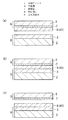
本実施形態では、有機デバイス1は例えば図3(a)に示されるように基材2上に第一の電極3、ホール輸送層42、発光層43、電子輸送層44、第二の電極5を備え、これらの層がこの順に積層して形成されることで得られる。また、有機デバイス1は例えば図3(b)に示されるように基材2上に第二の電極5、電子輸送層44、発光層43、ホール輸送層42、第一の電極3を備え、これらの層がこの順に積層して形成されることで得られる。また、有機デバイス1は例えば図3(c)に示されるように第二の電極5上に電子輸送層44、発光層43、ホール輸送層42、第一の電極3を備え、これらの層がこの順に積層して形成されることで得られる。
In the present embodiment, the
基材2は、例えばポリエステル、ポリオレフィン、ポリアミド、エポキシ等の樹脂、フッ素系樹脂等から任意の方法によって作製されたプラスチックフィルムやプラスチックシートなどの、可撓性を有するフィルム状又はシート状の部材から形成される。また、基材2はガラスなどの剛性を有する材料から形成されてもよい。
The
本実施形態において,第一の電極3は陽極として機能する。本実施形態において、陽極は発光層43にホールを注入するための電極である。陽極の材料としては、仕事関数の大きい金属、合金、電気伝導性化合物、これらの混合物などが用いられることが好ましい。特に仕事関数が4eV以上の材料が用いられることが好ましい。このような陽極の材料の具体例としては、金などの金属;CuI、ITO(インジウム−スズ酸化物)、SnO2、ZnO、IZO(インジウム−亜鉛酸化物)、GZO(ガリウム−亜鉛酸化物)等;PEDOT、ポリアニリン等の導電性高分子;任意のアクセプタ等でドープされた導電性高分子;カーボンナノチューブなどの導電性光透過性材料などが挙げられる。
In the present embodiment, the
第一の電極3は、例えば前記のような材料が基材2の表面上に真空蒸着法、スパッタリング法、塗布法等の適宜の手法で成膜されることで形成される。
The
第一の電極3に光透過性が要求される場合には、第一の電極3の光透過率が70%以上であることが好ましい。第一の電極3のシート抵抗は数百Ω/□以下であることが好ましく、100Ω/□以下であれば更に好ましい。
When the
第一の電極3の厚みは、この第一の電極3の光透過率、シート抵抗等の特性が上記のように調整されるためには、材料によって異なるが、500nm以下であることが好ましく、10〜200nmの範囲であれば更に好ましい。
The thickness of the
本実施形態において,第二の電極5は陰極として機能する。本実施形態において、陰極は、発光層43に電子を注入するための電極である。陰極の材料は、仕事関数の小さい金属、合金、電気伝導性化合物、これらの混合物などが好ましい。陰極の材料の仕事関数が5eV以下であれば特に好ましい。このような陰極の材料の具体例としてはアルカリ金属、アルカリ金属のハロゲン化物、アルカリ金属の酸化物、アルカリ土類金属等、及びこれらと他の金属との合金が挙げられ、更に具体的にはナトリウム、ナトリウム−カリウム合金、リチウム、マグネシウム、マグネシウム−銀混合物、マグネシウム−インジウム混合物、アルミニウム−リチウム合金、Al/LiF混合物等が挙げられる。陰極の材料として、アルミニウム、Al/Al2O3混合物なども使用可能である。陰極の発光層43側の面上にはアルカリ金属の酸化物、アルカリ金属のハロゲン化物、金属酸化物などから形成される電子注入層が重ねられていてもよく、また陰極は金属等の導電材料から形成される1層以上の層から構成されてもよい。このような電子注入層と陰極の積層構造としては、例えばアルカリ金属/Alの積層、アルカリ金属のハロゲン化物/アルカリ土類金属/Alの積層、アルカリ金属の酸化物/Alの積層などが挙げられる。陰極が光反射性の電極である場合には、透明な陰極と光反射性の層とが組み合わされることで光反射性の陰極が構成されてもよい。
In the present embodiment, the
陰極が光透過性の電極として形成される場合には、陰極がITO、IZOなどに代表される透明な電極材料から形成されてもよい。この場合、陰極が基材2上に形成されてもよい。
When the cathode is formed as a light transmissive electrode, the cathode may be formed from a transparent electrode material typified by ITO, IZO or the like. In this case, the cathode may be formed on the
第二の電極5と直接重なる有機層4にはリチウム、ナトリウム、セシウム、カルシウム等のアルカリ金属、アルカリ土類金属がドープされてもよい。
The
第二の電極5は、例えば前記のような材料が真空蒸着法、スパッタリング法、塗布法等の適宜の手法で成膜されることで形成される。
The
第二の電極5が光反射性の電極である場合には第二の電極5の光透過率が10%以下であることが好ましい。一方、第二の電極5が光透過性の電極である場合には、第二の電極5の光透過率が70%以上であることが好ましい。
When the
第二の電極5の厚みは、第二の電極5の光透過率等の特性が適宜調整されるためには、材料によって異なるが、500nm以下であることが好ましく、100〜200nmの範囲でれば更に好ましい。
The thickness of the
尚、上述のとおり第二の電極5は基材2上に形成されてもよい。また、第二の電極5がその上に積層される層を支持する機能を発揮する場合には、第二の電極5が導電性を有する金属板、金属箔、金属フィルムなどから構成されてもよい。
As described above, the
有機層4としては、次に示す発光層43、ホール輸送層42、ホール注入層41、電子輸送層44などが挙げられる。有機デバイス1はこれらの有機層4のうち少なくとも発光層43を備える。
Examples of the
<発光層>
発光層43は、陰極または電子輸送層44から発光層43に注入される電子と陽極又はホール輸送層42から発光層43に注入されるホールとが発光層43内で再結合することで発光する層である。発光層43の材料としては、有機エレクトロルミネッセンス素子用の材料として知られる任意の材料が使用可能である。このような発光層43の材料としては、特に制限されないが、好ましくはカルバゾール誘導体、ジスチリルベンゼン誘導体、ジスチリルアリーレン誘導体、ジスチリルアミン誘導体、トリアリールアミン誘導体、芳香族ボラン誘導体、含窒素複素環化合物、チオフェン誘導体、フラン誘導体、フルオレン誘導体、ポリフルオレン誘導体、ポリフェニレンビニレン誘導体、各種蛍光色素等が挙げられる。発光層43の材料として前述の材料系およびその誘導体を始めとするものが挙げられる。これらの化合物から選択される二種以上が併用されてもよい。
<Light emitting layer>
The
発光層43の材料として、マトリクスとなるホスト材料と、発光を担うドーパント材料(ゲスト材料)とが組み合わせれて用いられてもよい。ホスト材料としては、構造的には特に制限はないが、代表的には前述のカルバゾール誘導体、トリアリールアミン誘導体、芳香族ボラン誘導体、含窒素複素環化合物、チオフェン誘導体、フラン誘導体、オリゴアリーレン化合物等の基本骨格を有するものなどが挙げられる。ドーパント材料としては、前記化合物に代表される蛍光発光を生じる化合物のみならず、スピン多重項からの発光を示す材料系、例えば燐光発光を生じる燐光発光材料、例えば、イリジウム錯体化合物、白金錯体化合物、オスミウム錯体化合物や希土類錯体化合物など、およびそれらからなる部位を分子内の一部に有する化合物も好適に用いることができる。
As a material of the
本実施形態において特に好ましい発光層43の材料の例としては、フルオレン誘導体である2,7-bis(4'-hexyl-[1,1'biphenyl]-4-yl)-9,9'-spirobi[fluorene](BHBPSF)、4,4'-(9,9'-spirobi[fluorene]-2,7-diyl)bis(N,N-diphenylaniline)(SFBDPA)、2,7-bis(4-(9H-carbazol-9-yl)phenyl)-9,9'-spirobi[fluorene](SFP-Cz);ポリフルオレン誘導体であるPoly[{9,9-dihexyl-2,7-bis(1-cyanovinylene)fluorenylene}-alt-co-{2,5-bis(N,N'-di-phenylamino)-1,4-phenylene}];カルバゾール誘導体であるPoly(9-vinylcarbazole)が、挙げられる。
An example of a particularly preferable material for the light-emitting
ホスト材料とゲスト材料とが組み合わされる場合、本実施形態において特に好ましいホスト材料としては、カルバゾール誘導体である1,3-Bis(carbazol-9-yl)benzene(m-CP)、4,4'-Bis(carbazol-9-yl)biphenyl(CBP)、4,4'-Bis(carbazol-9-yl)-2,2'-dimethylbiphenyl(CDBP)、2,2'-bis(4-(carbazol-9-yl)phenyl)-biphenyl(BCBP);並びにDibenzo{[f,f']-4,4',7,7'-tetraphenyl}diindeno[1,2,3-cd:1',2',3'-lm]perylene(DBP)などが挙げられる。また本実施形態において特に好ましいゲスト材料としては、Tris(2-phenylpyridine)iridium(III)(Ir(ppy)3)、Tris[2-(p-tolyl)pyridine]iridium(III)(Ir(mppy)3)などが挙げられる。 When the host material and the guest material are combined, particularly preferred host materials in the present embodiment include 1,3-Bis (carbazol-9-yl) benzene (m-CP), 4,4′-, which is a carbazole derivative. Bis (carbazol-9-yl) biphenyl (CBP), 4,4'-Bis (carbazol-9-yl) -2,2'-dimethylbiphenyl (CDBP), 2,2'-bis (4- (carbazol-9 -yl) phenyl) -biphenyl (BCBP); and Dibenzo {[f, f ']-4,4', 7,7'-tetraphenyl} diindeno [1,2,3-cd: 1 ', 2', 3 '-lm] perylene (DBP). In addition, particularly preferred guest materials in the present embodiment include Tris (2-phenylpyridine) iridium (III) (Ir (ppy) 3), Tris [2- (p-tolyl) pyridine] iridium (III) (Ir (mppy) 3).
<ホール輸送層>
ホール輸送層42の材料は、例えばホール輸送性を有する化合物の群から選定される。この種の化合物としては、特に限定されないが、例えば、4,4'-bis[N-naphthyl-N-phenylamino]-biphenyl(α−NPD)、N,N'-bis(3-methylphenyl)-(1,1'-biphenyl)-4,4'diamine(TPD)、2−TNATA、4,4’,4”−トリス(N−(3−メチルフェニル)N−フェニルアミノ)トリフェニルアミン(MTDATA)、4,4’−N,N’−ジカルバゾールビフェニル(CBP)、スピロ−NPD、スピロ−TPD、スピロ−TAD、TNBなどを代表例とするトリアリールアミン系化合物;カルバゾール基を含むアミン化合物;フルオレン誘導体を含むアミン化合物など;、並びにこれらの基を導入した高分子化合物などが挙げられる。これらの材料は、電子ブロック層の材料としても用いられ得る。本実施形態において特に好ましいホール輸送層42の材料としては、4,4’−ビス[N−(ナフチル)−N−フェニル−アミノ]ビフェニル(α−NPD)、N,N’−ビス(3−メチルフェニル)−(1,1’−ビフェニル)−4,4’−ジアミン(TPD)、4,4’−N,N’−ジカルバゾールビフェニル(CBP)、2,2'-bis(4-(carbazol-9-yl)phenyl)-biphenyl(BCBP)が挙げられる。
<Hole transport layer>
The material of the
<ホール注入層>
ホール注入層41の材料としては、特に限定されず、一般に知られる任意のホール注入材料が用いられ得る。ホール注入層41の材料の好ましい例としては、銅フタロシアニン(CuPc)やトリアリールアミン誘導体などの低分子量の有機化合物、ポリエチレンジオキシチオフェン/ポリスチレンスルホン酸(PEDOT:PSS)などの高分子材料が挙げられる。なお、ホー輸送層に用いられる材料であって、ホールの注入性が良いものであれば、これに用いても構わない。本実施形態において特に好ましい例として、N4,N4'-(biphenyl-4,4'-diyl)bis(N4,N4',N4'-triphenylbiphenyl-4,4'-diamine)(TPT1)が挙げられる。
<Hole injection layer>
The material of the
<電子輸送層>
電子輸送層44の材料は、例えば電子輸送性を有する化合物の群から適宜選定される。この種の化合物としては、特に制限されず、一般に知られる任意の電子輸送材料が用いられ得る。電子輸送層44の材料として特に電荷輸送性の高い材料が使用されることが好ましい。このような電子輸送層44の材料の例としては、フェナントロリン誘導体、ピリジン誘導体、イミダゾール誘導体、トリアジン誘導体、テトラジン誘導体、オキサジアゾール誘導体等のヘテロ環を有する化合物、フォスフィンオキサイド化合物などが挙げられる。これらの材料は、ホールブロック層の材料としても用いられ得る。
<Electron transport layer>
The material of the
<材料種>
これらの有機層4を構成する有機材料は、各有機層4に相応しい特性を有するのであれば、上記の材料に限られない。また、この有機材料としては、低分子材料、オリゴマー材料、デンドリマー材料、高分子材料などが使用されることができ、またこれらの混合物が使用されることもできる。特に本実施形態では転写法への適用が困難な低分子材料が使用される場合でも、転写法により有機層4を効率良く、且つ歩留まりよく形成することができるという利点がある。尚、ここでは低分子材料とは、分子量が1200以下の材料をいう。低分子材料の分子量分布は単一分散(単分散)であることが好ましい。また有機層4を構成する有機材料には、この有機材料の特性が阻害されない範囲で造膜性を向上させる物質が添加されていてもよい。
<Material type>
The organic materials constituting these
<製法>
本実施形態では、有機デバイス1における一層又は複数層の有機層4のうち少なくとも一つが、図1,2に示されるような転写法により形成される。有機デバイス1が複数の有機層4を備える場合に全ての有機層4が転写法で形成されてもよい。
<Production method>
In the present embodiment, at least one of the
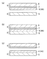
転写法により有機層4が形成されるにあたっては、離型層7を備える転写用部材9が使用される。転写用部材9は、例えばシート状の基材(ドナー基材6)と、このドナー基材6上に形成されている離型層7とを備える。
When the
ドナー基材6は柔軟性を有するシート状の部材であることが好ましい。ドナー基材6として、例えば、ポリエステル、ポリオレフィン、ポリアミド、エポキシ等の樹脂、フッ素系樹脂等から任意の方法によって作製されたプラスチックフィルムやプラスチックシートなどの、可撓性を有するフィルム状又はシート状の部材から形成される。また、基材2を備える有機デバイス1が製造される場合において、基材2が可撓性を有するフィルム状又はシート状の部材から形成される場合は、ドナー基材6は可撓性を有するフィルム状又はシート状の部材から形成されてもよく、ガラスなどの剛性を有する材料から形成されてもよい。すなわち、基材2とドナー基材6とのうち少なくとも一方が可撓性を有するフィルム状又はシート状の部材から形成されることが好ましい。特に、基材2が剛性を有する材料から形成され或いは可撓性を有するフィルム状又はシート状の部材から形成されると共に、ドナー基材6が可撓性を有するフィルム状又はシート状の部材から形成されることが好ましい。
The
離型層7は、有機層4の転写時における転写用部材9からの有機層4の剥離性を向上する機能を有する。
The
離型層7は適宜の材質から形成され得るが、シリコーン系材料から形成されることが好ましく、特にポリ(モノメチルシロキサン)などのシロキサンから構成されることが好ましい。この場合、有機材料から形成される有機層4が、離型層7から容易に剥離しやすくなる。
The
離型層7は、例えば次に示す(A)成分、(B)成分、及び(C)成分を含有するシリコーン組成物から形成される。
(A)下記一般式(I)で表わされる加水分解性オルガノシランを有機溶媒または水に分散されたコロイド状シリカ中で、X1モル当量に対し水0.001〜0.5モルを使用する条件下で部分加水分解することで調製される溶液。
R3 kSiX4−k …(I)
(式中、R3は同一または異種の置換もしくは非置換の炭素数1〜8の1価炭化水素基を示し、kは0〜3の整数、Xは加水分解性基を示す。)
(B)平均組成式が下記式(II)で表わされ、その分子中に少なくともシラノ−ル基を含有するポリオルガノシロキサン。
R4 aSi(OH)bO(4−a−b)/2 …(II)
(式中、R4は同一または異種の置換もしくは非置換の炭素数1〜8の1価炭化水素基を示し、aおよびbはそれぞれ0.2≦a≦2、0.0001≦b≦3、a+b<4の関係を満たす数である。)
(C)硬化触媒。
The
(A) Conditions under which 0.001 to 0.5 mol of water is used per 1 mol equivalent of X in colloidal silica in which a hydrolyzable organosilane represented by the following general formula (I) is dispersed in an organic solvent or water Solution prepared by partial hydrolysis underneath.
R 3 k SiX 4-k (I)
(Wherein R 3 represents the same or different substituted or unsubstituted monovalent hydrocarbon group having 1 to 8 carbon atoms, k represents an integer of 0 to 3, and X represents a hydrolyzable group.)
(B) A polyorganosiloxane having an average composition formula represented by the following formula (II) and containing at least a silanol group in the molecule.
R 4 a Si (OH) b O (4-ab) / 2 (II)
Wherein R 4 is the same or different substituted or unsubstituted monovalent hydrocarbon group having 1 to 8 carbon atoms, and a and b are 0.2 ≦ a ≦ 2, 0.0001 ≦ b ≦ 3, respectively. And a + b <4.)
(C) Curing catalyst.
(A)成分は、例えば有機溶媒あるいは水に分散されたコロイド状シリカに、一般式(I)で表される加水分解性基含有オルガノシランの1種または2種以上が加えられ、この加水分解性基含有オルガノシランがコロイド状シリカ中の水あるいは別途添加された水の存在下で部分加水分解されることで、調製される。 As the component (A), for example, one or more hydrolyzable group-containing organosilanes represented by the general formula (I) are added to colloidal silica dispersed in an organic solvent or water. The functional group-containing organosilane is prepared by partial hydrolysis in the presence of water in colloidal silica or separately added water.
一般式(I)で表される加水分解性基含有オルガノシランにおいて、一般式(I)中のR3は炭素数1〜8の置換または非置換の1価の炭化水素基を示し、その具体例としては、メチル基、エチル基、プロピル基、ブチル基、ペンチル基、ヘキシル基、へプチル基、オクチル基などの鎖状アルキル基;シクロペンチル基、シクロヘキシル基などのシクロアルキル基;2−フェニルエチル基、3−フェニルプロピル基などのアラルキル基;フェニル基、トリル基のようなアリール基;ビニル基、アリル基のようなアルケニル基;クロロメチル基、γ−クロロプロピル基、3,3,3−トリフルオロプロピル基のようなハロゲン置換炭化水素基;およびγ−メタクリロキシプロピル基、γ−メルカプトプロピル基などの置換炭化水素が挙げられる。これらの中でも合成の容易さ、あるいは入手の容易さから炭素数1〜4のアルキル基およびフェニル基が好ましい。加水分解性基であるXとしては、例えばアルコキシ基、アセトキシ基、オキシム基、エノキシ基、アミノ基、アミノキシ基、アミド基などが挙げられる。このうち、入手の容易さおよびシリカ分散オリゴマー溶液が調製されやすくなることからアルコキシ基が好ましい。 In the hydrolyzable group-containing organosilane represented by the general formula (I), R 3 in the general formula (I) represents a substituted or unsubstituted monovalent hydrocarbon group having 1 to 8 carbon atoms. Examples include a chain alkyl group such as a methyl group, an ethyl group, a propyl group, a butyl group, a pentyl group, a hexyl group, a heptyl group and an octyl group; a cycloalkyl group such as a cyclopentyl group and a cyclohexyl group; 2-phenylethyl Groups, aralkyl groups such as 3-phenylpropyl group; aryl groups such as phenyl group and tolyl group; alkenyl groups such as vinyl group and allyl group; chloromethyl group, γ-chloropropyl group, 3,3,3- And halogen-substituted hydrocarbon groups such as trifluoropropyl group; and substituted hydrocarbons such as γ-methacryloxypropyl group and γ-mercaptopropyl group. Among these, an alkyl group having 1 to 4 carbon atoms and a phenyl group are preferable because of easy synthesis or availability. Examples of X that is a hydrolyzable group include an alkoxy group, an acetoxy group, an oxime group, an enoxy group, an amino group, an aminoxy group, and an amide group. Among these, an alkoxy group is preferable because it is easily available and a silica-dispersed oligomer solution is easily prepared.
このような一般式(I)で表される加水分解性基含有オルガノシランとしては、一官能性(k=3)、二官能性(k=2)、三官能性(k=1)、及び四官能性(k=0)の、アルコキシシラン類、アセトキシシラン類、オキシムシラン類、エノキシシラン類、アミノシラン類、アミノキシシラン類、アミドシラン類などが挙げられる。これらの中でも入手の容易さ、およびシリカ分散オルガノシランオリゴマ−溶液が調製されやすいことから、アルコキシシラン類が好ましい。アルコキシシラン類のうち、テトラアルコキシシラン(k=0)としてはテトラメトキシシラン、テトラエトキシシランなどが例示され、オルガノトリアルコキシシラン(k=1)としてはメチルトリメトキシシラン、メチルトリエトキシシラン、メチルトリイソプロポキシシラン、フェニルトリメトキシシラン、フェニルトリエトキシシラン、3,3,3−トリフルオロプロピルトリメトキシランなどが例示される。また、ジオルガノジアルコキシシラン(k=2)としては、ジメチルジメトキシシラン、ジメチルジエトキシシラン、ジフェニルジメトキシシラン、ジフェニルジエトキシシラン、メチルフェニルジメトキシシランなどが例示され、トリオルガノアルコキシシラン(k=3)としてはトリメチルメトキシシラン、トリメチルエトキシシラン、トリメチルイソプロポキシシラン、ジメチルイソブチルメトキシシラなどが例示される。さらに一般にシランカップリング剤と呼ばれるオルガノシラン化合物もアルコキシシラン類に含まれる。 Examples of the hydrolyzable group-containing organosilane represented by the general formula (I) include monofunctional (k = 3), bifunctional (k = 2), trifunctional (k = 1), and Examples include tetrafunctional (k = 0) alkoxysilanes, acetoxysilanes, oxime silanes, enoxysilanes, aminosilanes, aminoxysilanes, and amidosilanes. Among these, alkoxysilanes are preferred because they are easily available and silica-dispersed organosilane oligomer solutions are easily prepared. Among the alkoxysilanes, examples of the tetraalkoxysilane (k = 0) include tetramethoxysilane and tetraethoxysilane, and examples of the organotrialkoxysilane (k = 1) include methyltrimethoxysilane, methyltriethoxysilane, and methyl. Examples include triisopropoxysilane, phenyltrimethoxysilane, phenyltriethoxysilane, 3,3,3-trifluoropropyltrimethoxylane and the like. Examples of the diorganodialkoxysilane (k = 2) include dimethyldimethoxysilane, dimethyldiethoxysilane, diphenyldimethoxysilane, diphenyldiethoxysilane, and methylphenyldimethoxysilane. Triorganoalkoxysilane (k = 3) ) Is exemplified by trimethylmethoxysilane, trimethylethoxysilane, trimethylisopropoxysilane, dimethylisobutylmethoxysila and the like. Furthermore, organosilane compounds generally called silane coupling agents are also included in the alkoxysilanes.
(A)成分においては、一般式(I)で表される加水分解性基含有オルガノシラン全体のうち三官能性(k=1)の化合物の割合が50モル%以上であることが好ましく、60モル%以上であれば更に好ましく、70モル%以上であれば最も好ましい。この場合、シリコーン組成物の塗膜硬度が十分に高くなると共に、このシリコーン組成物が乾燥硬化性に優れるようになる。 In the component (A), the proportion of the trifunctional (k = 1) compound in the entire hydrolyzable group-containing organosilane represented by the general formula (I) is preferably 50 mol% or more. If it is more than mol%, it is still more preferable, and it is most preferable if it is 70 mol% or more. In this case, the coating film hardness of the silicone composition becomes sufficiently high, and the silicone composition becomes excellent in dry curability.
(A)成分中のコロイド状シリカによって、シリコーン組成物から形成される硬化被膜の硬度が向上し、この硬化被膜の平滑性、耐クラック性が改善する。このコロイド状シリカとしては、水分散性を有するコロイド状シリカ、及びアルコールなどの非水系の有機溶媒分散性を有するコロイド状シリカが挙げられる。一般にこの様なコロイド状シリカは固形分としてのシリカを20〜50質量%含有している。また、水分散性コロイド状シリカが使用される場合、この水分散性コロイド状シリカ中の水は後述するように硬化剤として機能し得る。水分散性コロイド状シリカは、通常は水ガラスから調製される。このようなコロイド状シリカとして市販品が容易に入手される。また有機溶媒分散コロイド状シリカは水分散性コロイド状シリカの水が有機溶媒と置換されることで容易に調製される。このような有機溶剤分散コロイド状シリカとして、市販品が容易に入手される。有機溶剤分散コロイド状シリカにおける有機溶媒の種類としては、例えばメタノ−ル、エタノ−ル、イソプロパノ−ル、n−ブタノ−ル、イソブタノ−ル等の低級脂肪族アルコ−ル類;エチレングリコ−ル、エチレングリコ−ルモノブチルエ−テル、酢酸エチレングリコ−ルモノエチルエ−テル等のエチレングリコ−ル誘導体;ジエチレングリコ−ル、ジエチレングリコ−ルモノブチルエ−テル等のジエチレングリコ−ルの誘導体及びジアセトンアルコ−ル等が挙げられる。これらの有機溶媒のうち一種のみが用いられ、或いは二種以上が併用され得る。また、これらの親水性の有機溶剤と共に、トルエン、キシレン、酢酸エチル、酢酸ブチル、メチルエチルケトン、メチルイソブチルケトン、メチルエチルケトオキシムなどが併用されてもよい。 The hardness of the cured film formed from the silicone composition is improved by the colloidal silica in the component (A), and the smoothness and crack resistance of the cured film are improved. Examples of the colloidal silica include colloidal silica having water dispersibility and colloidal silica having dispersibility of a non-aqueous organic solvent such as alcohol. In general, such colloidal silica contains 20 to 50% by mass of silica as a solid content. When water-dispersible colloidal silica is used, the water in the water-dispersible colloidal silica can function as a curing agent as will be described later. Water dispersible colloidal silica is usually prepared from water glass. Commercial products are easily obtained as such colloidal silica. The organic solvent-dispersed colloidal silica is easily prepared by replacing the water of the water-dispersible colloidal silica with an organic solvent. As such organic solvent-dispersed colloidal silica, commercially available products are easily obtained. Examples of the organic solvent in the organic solvent-dispersed colloidal silica include lower aliphatic alcohols such as methanol, ethanol, isopropanol, n-butanol and isobutanol; ethylene glycol And ethylene glycol derivatives such as ethylene glycol monobutyl ether and ethylene glycol monoethyl ether; diethylene glycol derivatives such as diethylene glycol and diethylene glycol monobutyl ether, and diacetone alcohol. Only one of these organic solvents can be used, or two or more can be used in combination. In addition to these hydrophilic organic solvents, toluene, xylene, ethyl acetate, butyl acetate, methyl ethyl ketone, methyl isobutyl ketone, methyl ethyl ketoxime, and the like may be used in combination.
(A)成分中においてコロイド状シリカはシリカ固形分として5〜95質量%の範囲で含有されるのが好ましく、より好ましくは10〜90質量%であり、最も好ましくは20〜85質量%の範囲である。例えば、その含有量が5質量%未満であると所望の被膜硬度が得られず、また95質量%を超えるとシリカの均一分散が困難となり(A)成分がゲル化するなどの不都合をまねくことがある。 In the component (A), the colloidal silica is preferably contained in the range of 5 to 95% by mass as the silica solid content, more preferably 10 to 90% by mass, and most preferably in the range of 20 to 85% by mass. It is. For example, if the content is less than 5% by mass, the desired film hardness cannot be obtained, and if it exceeds 95% by mass, the uniform dispersion of silica becomes difficult and the (A) component gels. There is.
(A)成分におけるシリカ分散オリゴマーは、通常、加水分解性基含有オルガノシランがコロイド状シリカの存在下で部分加水分解することで得られる。加水分解性オルガノシランを部分加水分解させるに当たっての水の使用量は、加水分解性基(X)1モル当量に対して水0.001〜0.5モルとなる範囲であることが好ましい。例えば、水の使用量が0.001モル未満だと十分な部分加水分解物が得られず、0.5モルを越えると部分加水分解物の安定性が悪くなるからである。この部分加水分解する方法は特に限定されず、加水分解性オルガノアルコキシシランとコロイド状シリカとを混合して、必要量の水を添加配合すればよく、このとき部分加水分解反応は常温で進行する。なお、部分加水分解反応を促進させるため60〜100℃に加温してもよく、さらに部分加水分解反応を促進させる目的で、塩酸、酢酸、ハロゲン化シラン、クロロ酢酸、クエン酸、安息香酸、ジメチルマロン酸、蟻酸、プロピオン酸、グルタル酸、グリコ−ル酸、マレイン酸、マロン酸、トルエンスルホン酸、シュウ酸などの有機酸および無機酸を触媒に用いてもよい。 The silica-dispersed oligomer in component (A) is usually obtained by partially hydrolyzing a hydrolyzable group-containing organosilane in the presence of colloidal silica. The amount of water used for partially hydrolyzing the hydrolyzable organosilane is preferably in the range of 0.001 to 0.5 mol of water with respect to 1 mol equivalent of the hydrolyzable group (X). For example, if the amount of water used is less than 0.001 mol, a sufficient partial hydrolyzate cannot be obtained, and if it exceeds 0.5 mol, the stability of the partial hydrolyzate becomes poor. The method of partial hydrolysis is not particularly limited, and a hydrolyzable organoalkoxysilane and colloidal silica may be mixed and added with a necessary amount of water. At this time, the partial hydrolysis reaction proceeds at room temperature. . In addition, in order to accelerate | stimulate partial hydrolysis reaction, you may heat at 60-100 degreeC, and also in order to accelerate | stimulate partial hydrolysis reaction, hydrochloric acid, an acetic acid, halogenated silane, chloroacetic acid, a citric acid, a benzoic acid, Organic acids and inorganic acids such as dimethylmalonic acid, formic acid, propionic acid, glutaric acid, glycolic acid, maleic acid, malonic acid, toluenesulfonic acid, and oxalic acid may be used as the catalyst.
(A)成分は長期的に安定して性能を得るためには、液のpHを2.0〜7.0、好ましくは2.5〜6.5、より好ましくは3.0〜6.0にするとよい。pHがこの範囲外であると、特に水の使用量が(I)式中の置換基X1モル当量に対し0.3モル以上で(A)成分の長期的な性能低下が著しい。(A)成分のpHがこの範囲外にあるときは、この範囲より酸性側であれば、アンモニア、エチレンジアミン等の塩基性試薬を添加して調整すれば良く、塩基性側のときも塩酸、硝酸、酢酸等の酸性試薬を用いて調整すれば良い。なお、その調整方法は特に限定されるものではない。 In order to obtain the component (A) stably in the long term, the pH of the liquid is 2.0 to 7.0, preferably 2.5 to 6.5, more preferably 3.0 to 6.0. It is good to. When the pH is outside this range, the amount of water used is 0.3 mol or more with respect to 1 mole equivalent of the substituent X in the formula (I), and the long-term performance deterioration of the component (A) is remarkable. When the pH of the component (A) is outside this range, it may be adjusted by adding a basic reagent such as ammonia or ethylenediamine if it is more acidic than this range. Adjustment may be performed using an acidic reagent such as acetic acid. The adjustment method is not particularly limited.
次に(B)成分について説明する。上述したように、この(B)成分は平均組成式:R4 aSi(OH)bO(4-a-b)/2(式中、R4は同一または異種の置換もしくは非置換の炭素数1〜8の1価炭化水素基を示し、aおよびbはそれぞれ0.2≦a≦2、0.0001≦b≦3、a+b<4の関係を満たす数である。)で表すことができる分子中にシラノール基を含有するポリオルガノシロキサンである。 Next, the component (B) will be described. As described above, the component (B) has an average composition formula: R 4 a Si (OH) b O (4-ab) / 2 (wherein R 4 is the same or different substituted or unsubstituted carbon number of 1). A monovalent hydrocarbon group of ˜8, wherein a and b are numbers satisfying the relations 0.2 ≦ a ≦ 2, 0.0001 ≦ b ≦ 3, and a + b <4, respectively. It is a polyorganosiloxane containing silanol groups.
式中R4としては上記(I)式中のR3と同じものが例示されるが、好ましくは、炭素数1〜4のアルキル基、フェニル基、ビニル基、γ−グリシドキシプロピル基、γ−メタクリロキシプロピル基、γ−アミノプロピル基、3,3,3−トリフルオロプロピル基などの置換炭化水素基、より好ましくはメチル基およびフェニル基である。また式(II)中のaおよびbはそれぞれ上記の関係を満たす数であり、aが0.2未満またはbが3を超えると硬化被膜にクラックを生じるなどの不都合があり、また、aが2を超え4以下の場合またはbが0.0001未満では硬化がうまく進行しない。このようなシラノ−ル基含有ポリオルガノシロキサンはメチルトリクロロシラン、ジメチルジクロロシラン、フェニルトリクロロシラン、ジフェニルジクロロシラン、もしくはこれらに対応するアルコキシシランの1種もしくは2種以上の混合物を公知の方法により大量の水で加水分解することで得ることができる。シラノ−ル基含有ポリオルガノシロキサンを得るのに、アルコキシシランを用いて公知の方法で加水分解した場合、加水分解されないアルコキシ基が微量に残る場合がある。つまりシラノ−ル基と極微量のアルコキシ基が共存するようなポリオルガノシロキサンが得られる事もあるが、この様なポリオルガノシロキサンを用いても差支えない。 In the formula, as R 4 , the same as R 3 in the above formula (I) is exemplified, but preferably an alkyl group having 1 to 4 carbon atoms, a phenyl group, a vinyl group, a γ-glycidoxypropyl group, Substituted hydrocarbon groups such as γ-methacryloxypropyl group, γ-aminopropyl group and 3,3,3-trifluoropropyl group, more preferably methyl group and phenyl group. Further, a and b in the formula (II) are numbers satisfying the above relationship, respectively, and when a is less than 0.2 or b is more than 3, there is a disadvantage such as a crack in the cured film. When it is more than 2 and 4 or less, or when b is less than 0.0001, curing does not proceed well. Such a silanol group-containing polyorganosiloxane can be prepared by a known method using a large amount of methyltrichlorosilane, dimethyldichlorosilane, phenyltrichlorosilane, diphenyldichlorosilane, or a mixture of one or more of the corresponding alkoxysilanes. It can be obtained by hydrolysis with water. When a silanol group-containing polyorganosiloxane is obtained and hydrolyzed by a known method using alkoxysilane, an unhydrolyzed alkoxy group may remain in a trace amount. In other words, a polyorganosiloxane in which a silanol group and a trace amount of alkoxy group coexist may be obtained, but such a polyorganosiloxane may be used.
(C)成分である硬化触媒は、上記のように(A)成分と(B)成分との縮合反応を促進し、被膜を硬化させるものである。このような触媒としては、アルキルチタン酸塩、オクチル酸錫およびジブチル錫ジラウレ−ト、ジオクチル錫ジマレ−ト等のカルボン酸の金属塩;ジブチルアミン−2−ヘキソエ−ト、ジメチルアミンアセテート、エタノールアミンアセテート等のアミン塩;酢酸テトラメチルアンモニウム等のカルボン酸第4級アンモニウム塩;テトラエチルペンタミンのようなアミン類;N−β−アミノエチル−γ−アミノプロピルトリメトキシシラン、N−β−アミノエチル−γ−アミノプロピルメチルジメトキシシラン等のアミン系シランカップリング剤;p−トルエンスルホン酸、フタル酸、塩酸等の酸類;アルミニウムアルコキシド、アルミニウムキレート等のアルミニウム化合物、水酸化カリウムなどのアルカリ触媒;テトライソプロピルチタネート、テトラブチルチタネート、チタニウムテトラアセチルアセトネート等のチタニウム化合物、メチルトリクロロシラン、ジメチルジクロロシラン、トリメチルモノクロロシラン等のハロゲン化シラン等が例示されるが、この他に(A)成分と(B)成分の縮合反応に有効なものであれば特に制限はない。 The curing catalyst which is the component (C) accelerates the condensation reaction between the component (A) and the component (B) and cures the coating as described above. Such catalysts include metal salts of carboxylic acids such as alkyl titanates, tin octylate and dibutyltin dilaurate, dioctyltin dimaleate; dibutylamine-2-hexoate, dimethylamine acetate, ethanolamine Amine salts such as acetate; quaternary ammonium salts of carboxylic acid such as tetramethylammonium acetate; amines such as tetraethylpentamine; N-β-aminoethyl-γ-aminopropyltrimethoxysilane, N-β-aminoethyl Amine amine silane coupling agents such as γ-aminopropylmethyldimethoxysilane; acids such as p-toluenesulfonic acid, phthalic acid and hydrochloric acid; aluminum compounds such as aluminum alkoxide and aluminum chelate; alkali catalysts such as potassium hydroxide; tetra Isopropyl titane And titanium compounds such as tetrabutyl titanate and titanium tetraacetylacetonate, and halogenated silanes such as methyltrichlorosilane, dimethyldichlorosilane, and trimethylmonochlorosilane. In addition to these, (A) component and (B) There is no particular limitation as long as it is effective for the condensation reaction of the components.
(A)成分および(B)成分の配合割合は、(A)成分1〜99質量部に対して(B)成分99〜1質量部であり、より好ましくは(A)成分5〜95質量部に対して(B)成分95〜5質量部、最も好ましくは(A)成分10〜90質量部に対して(B)成分90〜10質量部である。(A)成分が1質量部未満であると常温硬化性に劣り、また十分な被膜硬度が得られない。一方、99質量部を超えると硬化性が不安定でかつ良好な塗膜が得られないことがある。 The blending ratio of the component (A) and the component (B) is 99 to 1 part by weight of the component (B) with respect to 1 to 99 parts by weight of the component (A), more preferably 5 to 95 parts by weight of the component (A). The component (B) is 95 to 5 parts by mass, and most preferably the component (B) is 90 to 10 parts by mass with respect to the component (A) 10 to 90 parts by mass. When the component (A) is less than 1 part by mass, the room temperature curability is inferior and sufficient film hardness cannot be obtained. On the other hand, when it exceeds 99 parts by mass, the curability is unstable and a good coating film may not be obtained.
また、(C)成分である硬化触媒の添加量は(A)成分および(B)成分の合計量を100としてそれに対して0.0001〜10質量%であることが好ましく、より好ましくは0.0005〜8質量%であり、最も好ましくは0.0007〜5質量%である。0.0001質量%未満だと常温で硬化しない。また、10質量%を越えると耐熱性、耐候性が悪くなる。 Further, the addition amount of the curing catalyst as the component (C) is preferably 0.0001 to 10% by mass with respect to the total amount of the component (A) and the component (B) as 100, more preferably 0.00. It is 0005-8 mass%, Most preferably, it is 0.0007-5 mass%. If it is less than 0.0001% by mass, it does not cure at room temperature. Moreover, when it exceeds 10 mass%, heat resistance and a weather resistance will worsen.
(A)成分のシリカ分散オリゴマーに含有される加水分解性基と(B)成分のシラノ−ル基とは、(C)成分の硬化触媒存在下で、常温もしくは低温加熱することにより縮合反応して硬化被膜を形成する。従って、このシリコーン組成物は常温で硬化するときにも湿度の影響をほとんど受けない。また加熱処理により縮合反応を促進して硬化被膜を形成することができる。 The hydrolyzable group contained in the silica dispersion oligomer of component (A) and the silanol group of component (B) undergo a condensation reaction by heating at room temperature or low temperature in the presence of the curing catalyst of component (C). To form a cured coating. Therefore, this silicone composition is hardly affected by humidity even when cured at room temperature. Moreover, a condensation reaction can be accelerated | stimulated by heat processing and a hardened film can be formed.
このシリコーン組成物は、取扱いの容易さから各種有機溶媒で希釈して使用できる。このとき使用する有機溶媒の種類は、(A)成分あるいは(B)成分の一価炭化水素基の種類もしくは分子量の大きさによって選定することができるものであって、その有機溶媒としては、メタノ−ル、エタノ−ル、イソプロパノ−ル、n−ブタノ−ル、イソブタノ−ル等の低級脂肪族アルコ−ル類;エチレングリコ−ル、エチレングリコ−ルモノブチルエ−テル、酢酸エチレングリコ−ルモノエチルエ−テル等のエチレングリコ−ル誘導体;ジエチレングリコ−ル、ジエチレングリコ−ルモノブチルエ−テル等のジエチレングリコ−ルの誘導体及びトルエン、キシレン、ヘキサン、ヘプタン、酢酸エチル、酢酸ブチル、メチルエチルケトン、メチルイソブチルケトン、メチルエチルケトオキシム、ジアセトンアルコ−ル等を挙げることができ、これらからなる群より選ばれた1種もしくは2種以上のものを使用することができる。 This silicone composition can be diluted with various organic solvents for ease of handling. The type of organic solvent used at this time can be selected according to the type of monovalent hydrocarbon group or the molecular weight of component (A) or component (B). Lower aliphatic alcohols such as ethanol, ethanol, isopropanol, n-butanol, isobutanol; ethylene glycol, ethylene glycol monobutyl ether, ethylene glycol monoethyl ether, etc. Derivatives of diethylene glycol such as diethylene glycol and diethylene glycol monobutyl ether and toluene, xylene, hexane, heptane, ethyl acetate, butyl acetate, methyl ethyl ketone, methyl isobutyl ketone, methyl ethyl ketoxime, diacetone alcohol -You can list It can be used more than one or two selected from the group consisting.
シリコーン組成物が、下記式(VI)に示す平均組成を有する直鎖状ポリシロキサンジオールを更に含有することも好ましい。
H(R7 2SiO)mOH ・・・・・・(VI)
この式(VI)中のmは、m≧3であり、好ましくは10〜100である。また、式中のR7はR3と同様のものを示すものである。この直鎖状ポリシロキサンジオールは末端OH基以外の反応基を有していないため、反応性に比較的乏しい分子である。そのため、シリコーン組成物に配合された直鎖状ポリシロキサンジオールは、コーティング材中での完全な相溶性に欠け、超微粒子として分散しているので、容易に塗膜表面に配位、単分子層を形成するが、最終的には末端OH基がバルク樹脂と縮合反応し、塗膜表面に固定化される。その結果、R7基表面に極在化し、第1コート層との剥離性を向上させる効果を奏する。式中のmが比較的小さいものは相溶性に優れるため、塗膜表面で層を形成するだけではなく、バルクに取り込まれ事で塗膜に柔軟性を与え、クラック防止効果にもつながる。上記直鎖状ポリシロキサンジオールの含有量は、シリコーン組成物においてシリコーンを縮合ケイ素化合物として換算した質量及びシリカ質量の和に対して、0.1〜100質量%であることが好ましい。上記直鎖状ポリシロキサンジオールの含有量が0.1質量%未満であると、剥離性の発現が弱く、100質量%を越えると塗膜の硬化阻害を起こす要因となるためである。
It is also preferred that the silicone composition further contains a linear polysiloxane diol having an average composition represented by the following formula (VI).
H (R 7 2 SiO) m OH (VI)
M in the formula (VI) is m ≧ 3, preferably 10-100. R 7 in the formula represents the same as R 3 . Since this linear polysiloxane diol has no reactive group other than the terminal OH group, it is a molecule with relatively poor reactivity. For this reason, the linear polysiloxane diol blended in the silicone composition lacks complete compatibility in the coating material and is dispersed as ultrafine particles. In the end, the terminal OH group undergoes a condensation reaction with the bulk resin to be immobilized on the coating film surface. As a result, there is an effect that it is localized on the surface of the R 7 group and improves the peelability from the first coat layer. Those having a relatively small m in the formula are excellent in compatibility, and thus not only form a layer on the surface of the coating film, but also add flexibility to the coating film by being incorporated into the bulk, leading to a crack prevention effect. It is preferable that content of the said linear polysiloxane diol is 0.1-100 mass% with respect to the sum of the mass which converted silicone as a condensed silicon compound, and the mass of silica in a silicone composition. This is because if the content of the linear polysiloxane diol is less than 0.1% by mass, the release property is weak, and if it exceeds 100% by mass, the coating may be inhibited from being cured.
シリコーン組成物は、下記一般式(VII)で表され、且つR9が置換もしくは非置換の炭素数1〜9の1価炭化水素基である少なくとも1種の第1の(メタ)アクリル酸エステルと、下記一般式(VII)で表され、且つR9がエポキシ基、グリシジル基またはそれらを含む炭化水素基である少なくとも1種の第2の(メタ)アクリル酸エステルと、下記一般式(VII)で表され、且つR9がアルコキシシリル基もしくはハロゲン化シリル基を含む炭化水素基である少なくとも1種の第3のアクリル酸エステルまたはメタアクリル酸エステルと、を共重合させてなるアクリル樹脂共重合体を更に含有することも好ましい。このアクリル樹脂共重合体は、シリコーン組成物の塗膜の靱性を改善する作用を発揮する。
CH2=CR8(COOR9)・・・・・・・(VII)
(式中、R8は水素原子またはメチル基を表す。)
このアクリル樹脂共重合体は、上述したように、上記第1、第2及び第3の(メタ)アクリル酸エステルの共重合体である。第1の(メタ)アクリル酸エステルは、(VII)式中のR9が炭素数1〜9の置換または非置換の1価の炭化水素基、例えば、メチル基、エチル基、n−プロピル基、i−プロピル基、n−ブチル基、i−ブチル基、sec−ブチル基、tert−ブチル基、ペンチル基、ヘキシル基、へプチル基、オクチル基などのアルキル基;シクロペンチル基、シクロヘキシル基などのシクロアルキル基;2−フェニルエチル基、2−フェニルプロピル基、3−フェニルプロピル基などのアラルキル基;フェニル基、トリル基のようなアリール基;クロロメチル基、γ−クロロプロピル基、3,3,3−トリフルオロプロピル基などのハロゲン化炭化水素基;2−ヒドロキシエチル基などのヒドロキシ炭化水素基;などであるものの内の少なくとも1種以上である。また、第2の(メタ)アクリル酸エステルは、(VII)式中のR9がエポキシ基、グリシジル基またはそれらを含む炭化水素基、例えば、γ−グリシドキシプロピル基であるものの内の少なくとも1種である。第3の(メタ)アクリル酸エステルは(VII)式中のR9がアルコキシシリル基もしくはハロゲン化シリル基を含む炭化水素基、例えば、トリメトキシシリルプロピル基、ジメトキシメチルシリルプロピル基、モノメトキシジメチルシリルプロピル基、エトキシジメチルシリルプロピル基、トリクロロシリルプロピル基、ジクロロメチルシリルプロピル基、クロロジメチルシリルプロピルであるものの内の少なくとも1種である。このアクリル共重合体は、上記第1、第2及び第3の(メタ)アクリル酸エステル中、それぞれ少なくとも1種、合計少なくとも3種以上を含む(メタ)アクリル酸エステルの共重合体であり、上記第1、第2及び第3の(メタ)アクリル酸エステル中からさらに1種あるいは2種以上、あるいは上記以外の(メタ)アクリル酸エステルの中から選ばれたさらに1種あるいは2種以上を含む共重合体であっても構わない。
The silicone composition is represented by the following general formula (VII), and at least one first (meth) acrylic acid ester in which R 9 is a substituted or unsubstituted monovalent hydrocarbon group having 1 to 9 carbon atoms. And at least one second (meth) acrylic acid ester represented by the following general formula (VII) and R 9 is an epoxy group, a glycidyl group or a hydrocarbon group containing them, and the following general formula (VII And at least one third acrylic ester or methacrylic ester in which R 9 is a hydrocarbon group containing an alkoxysilyl group or a halogenated silyl group. It is also preferable to further contain a polymer. This acrylic resin copolymer exhibits the effect of improving the toughness of the coating film of the silicone composition.
CH 2 = CR 8 (COOR 9 ) (VII)
(In the formula, R 8 represents a hydrogen atom or a methyl group.)
As described above, this acrylic resin copolymer is a copolymer of the first, second and third (meth) acrylic acid esters. In the first (meth) acrylic acid ester, R 9 in the formula (VII) is a substituted or unsubstituted monovalent hydrocarbon group having 1 to 9 carbon atoms, such as a methyl group, an ethyl group, or an n-propyl group. Alkyl groups such as i-propyl group, n-butyl group, i-butyl group, sec-butyl group, tert-butyl group, pentyl group, hexyl group, heptyl group, octyl group; cyclopentyl group, cyclohexyl group, etc. Cycloalkyl group; aralkyl group such as 2-phenylethyl group, 2-phenylpropyl group and 3-phenylpropyl group; aryl group such as phenyl group and tolyl group; chloromethyl group, γ-chloropropyl group, 3, 3 , 3-trifluoropropyl group and other halogenated hydrocarbon groups; 2-hydroxyethyl group and other hydroxy hydrocarbon groups; It is. In addition, the second (meth) acrylic acid ester has at least R 9 in the formula (VII) in which R 9 is an epoxy group, a glycidyl group or a hydrocarbon group containing them, for example, a γ-glycidoxypropyl group. One type. The third (meth) acrylic acid ester is a hydrocarbon group in which R 9 in the formula (VII) contains an alkoxysilyl group or a halogenated silyl group, such as trimethoxysilylpropyl group, dimethoxymethylsilylpropyl group, monomethoxydimethyl At least one of silylpropyl, ethoxydimethylsilylpropyl, trichlorosilylpropyl, dichloromethylsilylpropyl, and chlorodimethylsilylpropyl. This acrylic copolymer is a copolymer of (meth) acrylic acid ester containing at least one kind and a total of at least three or more kinds in the first, second and third (meth) acrylic acid esters, One or more kinds selected from the first, second and third (meth) acrylic acid esters, or one or two or more kinds selected from other (meth) acrylic acid esters other than the above. It may be a copolymer containing.
上記第1の(メタ)アクリル酸エステルにより、シリコーン組成物の塗膜の靱性が改善する。このためには、R9の置換あるいは非置換炭化水素基がある程度以上の体積を持つことが望ましく、炭素数が2以上であることが好ましい。第3の(メタ)アクリル酸エステルが使用される場合、塗膜硬化時にアクリル樹脂共重合体と(A)成分及び(B)成分との間に化学結合させるものであって、これによりアクリル樹脂共重合体が塗膜中に固定化される。第3の(メタ)アクリル酸エステルには、シリコーン組成物を構成する成分間の相溶性を改善する効果もある。 The first (meth) acrylic acid ester improves the toughness of the coating film of the silicone composition. For this purpose, the substituted or unsubstituted hydrocarbon group of R 9 desirably has a volume of a certain level or more, and preferably has 2 or more carbon atoms. When the third (meth) acrylic acid ester is used, it is chemically bonded between the acrylic resin copolymer, the component (A) and the component (B) at the time of curing the coating film. The copolymer is immobilized in the coating film. The third (meth) acrylic acid ester also has an effect of improving the compatibility between the components constituting the silicone composition.
このアクリル樹脂共重合体の分子量は、(A)成分及び(B)成分との相溶性に大きく関わる。このアクリル樹脂共重合体のポリスチレン換算平均分子量が5万を越えると、相分離し、塗膜が白化することがある。従って、このアクリル樹脂共重合体のポリスチレン換算平均分子量は5万以下であることが望ましい。また、アクリル樹脂共重合体のポリスチレン換算平均分子量の下限は1000であることが望ましい。分子量が1000未満だと、塗膜の靱性が下がり、クラックが生じやすくなる傾向があり、好ましくない。アルコキシシリル基またはハロゲン化シリル基を持つ第3の(メタ)アクリル酸エステルは、共重合体中の単量体モル比率で2〜50質量%の範囲であることが望ましい。2質量%未満では、このアクリル樹脂共重合体と(A)成分及び(B)成分との相溶性が悪く、塗膜が白化することがある。また、50質量%を越えると、アクリル樹脂共重合体と(A)成分及び(B)成分との結合密度が高くなりすぎ、アクリル樹脂共重合体を添加することによる靱性の改善が十分に発揮されない。このアクリル樹脂共重合体の合成方法として、公知の有機溶媒中での溶液重合、乳化重合、懸濁重合によるラジカル重合法、アニオン重合法、カチオン重合法等が採用され得る。 The molecular weight of this acrylic resin copolymer is greatly related to the compatibility with the component (A) and the component (B). When the polystyrene-reduced average molecular weight of the acrylic resin copolymer exceeds 50,000, phase separation may occur and the coating film may be whitened. Therefore, it is desirable that this acrylic resin copolymer has an average molecular weight in terms of polystyrene of 50,000 or less. The lower limit of the polystyrene-reduced average molecular weight of the acrylic resin copolymer is desirably 1000. If the molecular weight is less than 1000, the toughness of the coating film tends to decrease and cracks tend to occur, which is not preferable. The third (meth) acrylic acid ester having an alkoxysilyl group or a halogenated silyl group is desirably in the range of 2 to 50% by mass in terms of the monomer molar ratio in the copolymer. If it is less than 2 mass%, the compatibility of this acrylic resin copolymer with the component (A) and the component (B) is poor, and the coating film may be whitened. On the other hand, when the content exceeds 50% by mass, the bond density between the acrylic resin copolymer, the component (A) and the component (B) becomes too high, and the improvement in toughness due to the addition of the acrylic resin copolymer is sufficiently exhibited. Not. As a method for synthesizing this acrylic resin copolymer, a solution polymerization in a known organic solvent, an emulsion polymerization, a radical polymerization method by suspension polymerization, an anionic polymerization method, a cationic polymerization method and the like can be employed.
このアクリル重合共重合体の含有量は、シリコーン組成物においてシリコーンを縮合ケイ素化合物として換算した質量及びシリカ質量の和に対して、0.1〜100質量%であることが好ましい。0.1質量%未満であると、靱性の発現が弱く、100質量%を越えると塗膜の硬化阻害を引き起こしてしまうからである。 The content of the acrylic copolymer is preferably 0.1 to 100% by mass with respect to the sum of the mass of silica converted to a condensed silicon compound and the mass of silica in the silicone composition. This is because if it is less than 0.1% by mass, the toughness is weakly expressed, and if it exceeds 100% by mass, the coating is hardened.
離型層7は、ドナー基材6上にシリコーン組成物を塗布乾燥することにより形成される。シリコーン組成物の塗布方法としては特に限定されるものではなく、例えばグラビアロールコーター、グラビアオフセットロールコーター、マイクログラビアロールコーター、絞りロールコーター、エアーナイフコーター、リバースロールコーター、バーコーター、ダイコーター、ファウンテンコーター、コンマーター、スプレー、ディッピング、フロー等の各種塗装方法から選択され得る。この際、シリコーン組成物には必要に応じてレベリング剤が添加されてもよい。乾燥条件はドナー基材6の耐熱温度によって適宜決定すればよく、例えば室温乾燥でもよい。また離型層7の厚みには特に制限はないが、例えば0.1〜20μmの範囲であり、特に転写時の転写用部材9の変形に対して離型層7がクラックを生じることなく追随するためには0.1〜15μmが望ましい。なお、剥離性やクラック防止性、柔軟性を改善するためにシリコーン組成物が上記直鎖状ポリシロキサンジオールやアクリル樹脂共重合体が含有している場合には、離型層7の厚みを比較的厚くすることができ、例えば厚みが0.1〜50μmの範囲であればよく、特に転写時の転写用部材9の変形に対して離型層7がクラックを生じることなく追随するためには0.1〜30μmがより望ましい。
The
離型層7の表面の水の接触角は90°以上であることが好ましい。この場合、離型層7上に形成される有機層4が転写時に離型層7から更に剥離しやすくなる。離型層7を上記のようにシリコーン組成物で形成し、且つ離型層7を形成する際にシリコーン組成物の反応を充分に進行させれば、離型層7の表面の水の接触角を90°以上とすることは容易である。
The contact angle of water on the surface of the
また、離型層7の表面の水の接触角は90°以上とするためには、離型層7を形成する前に予めドナー基板6の表面に適宜の親水化処理を施しておくことも好ましい。この場合、ドナー基板6の親水化処理が施された表面上に離型層7を形成すると、離型層7を構成する分子中の親水基とドナー基板6の親水化処理された表面とが引き付け合い、このため離型層7内の表面側で親水基の密度が低下すると共に疎水基の密度が増大するようになり、これにより離型層7の表面の疎水性が向上してその水の接触角が大きくなる。
Further, in order to set the contact angle of water on the surface of the
また、離型層7の表面の水の接触角は90°以上とするためには、離型層7を形成する際、ドナー基板6上にシリコーン組成物を塗布乾燥して塗膜を形成し、この塗膜を有機溶媒を含む雰囲気中に曝露させながらシリコーン組成物の反応を進行させて離型層7を形成することも好ましい。雰囲気中に含有させる有機溶媒は、離型層7を形成するために使用されるシリコーン組成物中の有機溶媒と同じであることが好ましい。この場合、シリコーン組成物の反応が促進され、これにより離型層7の表面の疎水性が向上してその水の接触角が大きくなる。
Further, in order to set the contact angle of water on the surface of the
有機デバイス1における有機層4が転写法により形成される場合には、まず有機層4が転写用部材9の離型層7上に形成される。有機層4の厚みは、この有機層4の材質や機能などに応じて適宜設定される。
When the
有機層4を形成するにあたり、まず有機層4を構成する有機材料と、この有機材料が溶解すると共に離型層7に対して親和性を有する溶媒とを含有する塗布液10が調製される。
In forming the
有機材料が溶解すると共に離型層7に対して親和性を有する溶媒は、有機材料が溶解する第一の溶媒と離型層7に対して親和性を有する第二の溶媒とを含む混合溶媒であることが好ましい。この場合、有機材料が溶解すると共に離型層7に対して親和性を有する溶媒における、有機材料の溶解性と離型層7に対する親和性が容易に調整され得る。
The solvent having an affinity for the
混合溶媒の調製に使用される有機材料が溶解する第一の溶媒は、有機材料の種類に依存するものであり、特に限定されないが、その好ましい具体例としては、クロロホルム、1,2−ジクロロメタン、クロロベンゼン、ジクロロベンゼンなどのハロゲン系溶媒やテトラヒドロフランなどのフラン系溶媒が挙げられる。 The first solvent in which the organic material used for the preparation of the mixed solvent dissolves depends on the type of the organic material and is not particularly limited, but preferred specific examples thereof include chloroform, 1,2-dichloromethane, Examples thereof include halogen solvents such as chlorobenzene and dichlorobenzene, and furan solvents such as tetrahydrofuran.
混合溶媒の調製に使用される離型層7に対して親和性を有する第二の溶媒は、離型層7の組成に依存するものであり、特に限定されないが、離型層7がシリコーン系材料から形成される場合の第二の溶媒の好ましい例としてはアルコール類、ケトン類、低級アルキルアセテート類、フッ素系溶媒などが挙げられる。
The second solvent having an affinity for the
更に、第一の溶媒と第二の溶媒との沸点の差は小さくことが好ましく、特にこの沸点の差が20℃以内であることが好ましい。この場合、後述するように有機層4の成膜性が向上する。
Furthermore, the difference in boiling point between the first solvent and the second solvent is preferably small, and the difference in boiling point is particularly preferably within 20 ° C. In this case, as described later, the film formability of the
また、第一の溶媒の溶解度パラメータと、第二の溶媒の溶解度パラメータとが、いずれも10以下であることも好ましい。この場合、第一の溶媒と前記第二の溶媒の相溶性が高くなり、均一性の高い混合溶媒が得られるようになる。このため、混合溶媒の全体に亘ってこの混合溶媒が有機材料の溶解性を発揮すると共に離型層に対する親和性を発揮し、これにより有機層4の成膜性が更に向上する。
It is also preferred that the solubility parameter of the first solvent and the solubility parameter of the second solvent are both 10 or less. In this case, the compatibility of the first solvent and the second solvent is increased, and a highly uniform mixed solvent can be obtained. For this reason, this mixed solvent exhibits the solubility of the organic material and the affinity for the release layer over the entire mixed solvent, thereby further improving the film formability of the
混合溶媒の特に好ましい例として、第一の溶媒としてクロロホルム(沸点61.0℃、溶解度パラメータ9.3)を含有すると共に第二の溶媒としてアセトン(沸点56.1℃、溶解度パラメータ10.0)を含有する混合溶媒、第一の溶媒としてクロロホルム(沸点61.0℃、溶解度パラメータ9.3)を含有すると共に第二の溶媒として酢酸エチル(沸点79.5℃、溶解度パラメータ9.0)を含有する混合溶媒、第一の溶媒としてクロロホルム(沸点61.0℃、溶解度パラメータ9.3)を含有すると共に第二の溶媒としてメチルエチルケトン(沸点79.5℃、溶解度パラメータ9.3)を含有する混合溶媒、第一の溶媒としてテトラヒドロフラン(沸点66.0℃、溶解度パラメータ9.1)を含有すると共に第二の溶媒としてアセトン(沸点56.1℃、溶解度パラメータ10.0)を含有する混合溶媒、第一の溶媒としてジクロロメタン(沸点40.0℃、溶解度パラメータ9.7)を含有すると共に第二の溶媒としてアセトン(沸点56.1℃、溶解度パラメータ10.0)を含有する混合溶媒などが挙げられる。 As a particularly preferable example of the mixed solvent, chloroform (boiling point 61.0 ° C., solubility parameter 9.3) is contained as the first solvent, and acetone (boiling point 56.1 ° C., solubility parameter 10.0) is contained as the second solvent. A mixed solvent containing chloroform, chloroform (boiling point 61.0 ° C., solubility parameter 9.3) as the first solvent, and ethyl acetate (boiling point 79.5 ° C., solubility parameter 9.0) as the second solvent. Contains mixed solvent, first solvent as chloroform (boiling point 61.0 ° C., solubility parameter 9.3) and second solvent as methyl ethyl ketone (boiling point 79.5 ° C., solubility parameter 9.3) Containing a mixed solvent, tetrahydrofuran (boiling point 66.0 ° C., solubility parameter 9.1) as the first solvent, Mixed solvent containing acetone (boiling point 56.1 ° C., solubility parameter 10.0), dichloromethane as first solvent (boiling point 40.0 ° C., solubility parameter 9.7) and acetone as second solvent And a mixed solvent containing (boiling point 56.1 ° C., solubility parameter 10.0).
混合溶媒中の第一の溶媒と第二の溶媒との割合は特に制限されないが、前者対後者の体積比率が2:1〜1:2の範囲であることが好ましく、1:1〜1:2の範囲であれば更に好ましい。 The ratio of the first solvent and the second solvent in the mixed solvent is not particularly limited, but the volume ratio of the former to the latter is preferably in the range of 2: 1 to 1: 2, and 1: 1 to 1: A range of 2 is more preferable.
塗布液10中の有機材料の含有量は特に制限されず、塗布液10中に有機材料が均一に溶解し、有機層4の成膜性が良好となるように適宜設定される。
The content of the organic material in the
この塗布液10が離型層7上に塗布されることで、塗膜(湿潤塗膜)が形成される。離型層7上への塗布液10の塗布方法は特に制限されず、インクジェット印刷法、スクリーン印刷法、グラビア印刷法、オフセット印刷法、フレキソ印刷法、ディスペンサ印刷法、スリットコート法、ダイコート法、ドクターブレードコート法、ワイヤーバーコート法等の適宜の手法が採用され得る。
A coating film (wet coating film) is formed by applying the
離型層7上に形成された湿潤塗膜から溶媒を揮発させることで有機層4が形成される。この場合、常温下で湿潤塗膜から溶媒を揮発させてもよく、湿潤塗膜を加熱することで湿潤塗膜から溶媒を揮発させてもよい。湿潤塗膜を加熱する場合の加熱温度等の加熱条件は、溶媒の種類等に応じて適宜設定されるが、例えば第一の溶媒としてクロロホルム(沸点61.0℃)を含有すると共に第二の溶媒としてアセトン(沸点56.1℃)を含有する混合溶媒が用いられる場合には、60〜100℃で0.5〜3分間加熱することが好ましい。
The
このように離型層7上に有機層4が形成されると、離型層7上に湿潤塗膜が形成される際には塗布液10中の溶媒が有機材料が溶解させると共にこの溶媒が離型層7に対して親和性を有することから、むらが少なく均一性の高い湿潤塗膜が形成され得る。この湿潤塗膜から溶媒が揮発されることで、離型層7上にむらが少なく均一性の高い有機層4が形成される。
When the
塗布液10中の溶媒が第一の溶媒と第二の溶媒とを含む混合溶媒である場合には第一の溶媒と第二の溶媒との沸点が近いことが好ましく、特に上記のとおり沸点の差が20℃以内であることが好ましい。この場合、湿潤塗膜から溶媒が揮発する過程において、第一の溶媒に比べて第二の溶媒が過剰に揮発することで湿潤塗膜が離型層7から弾かれてしまったり、第二の溶媒に比べて第一の溶媒が過剰に揮発することで有機材料が凝集してしまったりすることが抑制される。これにより、離型層7上に形成される有機層4のむらが更に抑制され、この有機層4の均一性が更に向上する。
When the solvent in the
上記のように転写部材上に有機層4を形成する一方で、有機デバイス1の一部を構成する中間部材8も用意する。この中間部材8に、転写用部材9上の有機層4が転写される。
While forming the
中間部材8は、有機デバイス1の一部を構成する部材であって、転写用部材9上の有機層4が積層されるべき構造を有すればよい。中間部材8としては、例えば基材2及びこの基材2の上に重ねられている第一の電極3を備える部材;基材2、この基材2の上に重ねられている第一の電極3及びこの第一の電極3の上に重ねられている一層又は複数層の有機層4(転写用部材9上の有機層4とは異なる有機層4)を備える部材;基材2及びこの基材2の上に重ねられている第二の電極5を備える部材;基材2、この基材2の上に重ねられている第二の電極5及びこの第二の電極5の上に重ねられている一層又は複数層の有機層4(転写用部材9上の有機層4とは異なる有機層4)を備える部材などが挙げられる。また有機デバイス1が基材2を備えず、第二の電極5がこの第二の電極5の上に積層される層を支持する機能を発揮する場合には、中間部材8は第二の電極5のみからなる部材;第二の電極5及びその上に重ねられている一層又は複数層の有機層4(転写用部材9上の有機層4とは異なる有機層4)を備える部材などであってもよい。
The
図1に示す態様では中間部材8は基材2及びこの基材2の上に重ねられている第一の電極3を備える部材である。
In the embodiment shown in FIG. 1, the
このような中間部材8上に転写用部材9上の有機層4(図1に示す態様ではホール注入層41)が重ねられると共に押圧されることで、転写用部材9上の有機層4が中間部材8上に転写される。この際、有機層4の転写が促進されるためには、転写用部材9がこの転写用部材9から有機層4が離れやすくなるような適切な温度に保持されると共に、中間部材8がこの中間部材8に有機層4が密着しやすくなるような適切な温度に保持されることが好ましい。この転写時の中間部材8と転写用部材9の好ましい温度はこれらの部材及び有機層4の構成に依存するが、中間部材8よりも転写用部材9の温度の方が高いことが好ましく、例えば中間部材8が140℃、転写用部材9が80℃にそれぞれ保持されることが好ましい。
The
このように転写用部材9上の有機層4が中間部材8上に転写される際、基材2とドナー基材6とのうち少なくとも一方が可撓性を有するフィルム状又はシート状の部材から形成される場合には、中間部材8と転写用部材9のうち少なくとも一方を湾曲させながらこれらを押圧することが可能となる。そのため、転写用部材9上の有機層4が中間部材8上に更に転写されやすくなる。
Thus, when the
ホール注入層41が積層された中間部材8には、更にその上に有機層4であるホール輸送層42、発光層43、電子輸送層44などが積層され、更にその上に第二の電極5が重ねられる。これにより図3(a)に示されるような有機エレクトロルミネセンス素子1が得られる。有機層4の上に別の有機層4を重ねる際(例えばホール注入層41の上にホール輸送層42を重ねる際)には、中間部材8に有機層4が重ねられることで構成される部材を新たな中間部材8とみなし、この新たな中間部材8を用いて上述の方法を繰り返してもよい。
The
図2に示す態様では、図1に示す場合と同様のドナー基材6と離型層7とを備える転写用部材9における離型層7の表面上に有機層4として電子輸送層44が、上述のものと同じ手法により形成されている。、
一方、中間部材8は第二の電極5のみから構成されている。この場合の第二の電極5はその上に積層される層を支持する機能を発揮し、例えば導電性を有する金属板、金属箔、金属フィルムなどから構成される。
In the embodiment shown in FIG. 2, the
On the other hand, the
この場合も、中間部材8上に転写用部材9上の有機層4(図2に示す態様では電子輸送層44)が重ねられると共に押圧されることで、転写用部材9上の有機層4が中間部材8上に転写される。この際、図1に示す場合と同様に有機層4の転写が促進されるためには、転写用部材9がこの転写用部材9から有機層4が離れやすくなるような適切な温度に保持されると共に、中間部材8がこの中間部材8に有機層4が密着しやすくなるような適切な温度に保持されることが好ましい。
Also in this case, the
電子輸送層44が積層された中間部材8には、更にその上に有機層4である発光層43、ホール輸送層42、ホール注入層41などが積層され、更にその上に第一の電極3が重ねられる。これにより図3(c)に示されるような有機エレクトロルミネセンス素子1が得られる。有機層4の上に別の有機層4を重ねる際(例えば電子輸送層44の上に発光層43を重ねる際)には、中間部材8に有機層4が重ねられることで構成される部材を新たな中間部材8とみなし、この新たな中間部材8を用いて上述の方法を繰り返してもよい。
The
上述の手法により、有機デバイス1における一層又は複数層の有機層4が形成される。有機デバイス1が複数の有機層4を備える場合には、そのうち一部の有機層4が上述の方法により形成されてもよく、全ての有機層4が上述の方法により形成されてもよい。すなわち、例えば基材2上の第一の電極3上に有機層4として電子輸送層44、発光層43、ホール輸送層42が順次形成される場合には、これらの有機層4のうち一部の有機層4が上述の方法により形成されてもよく、全ての有機層4が上述の方法により形成されてもよい。複数の有機層4のうち一部の有機層4が上述の方法により形成される場合には、残りの有機層4は例えば蒸着法などの公知の方法により形成されてもよい。
The one or more
次に、上述の方法により有機デバイス1を作製するための装置について説明する。
Next, an apparatus for producing the
図4に、有機デバイス1の製造装置の一態様の概略構成が示されている。この装置は、長尺な転写用部材9を搬送する搬送部(第一搬送部)、中間部材8を搬送する搬送部(第二搬送部)、転写用部材9へ塗布液10を塗布する塗布部、転写用部材9を加熱する加熱部(第一加熱部17)、中間部材8を加熱する加熱部(第二加熱部18)、並びに中間部材8に転写用部材9の離型層7上の有機層4を押圧することで有機層4を離型層7上から中間部材8上へ転写する転写部とを備える。
FIG. 4 shows a schematic configuration of one aspect of the manufacturing apparatus of the
本態様では、第一搬送部は転写用部材9を巻回した状態で保持すると共にこの転写用基材2を繰り出す繰出機11と、繰出機11から繰り出された転写用部材9を巻き取る巻取機12と、この繰出機11と巻取機12との間における転写用部材9の搬送経路上に設けられている押圧ロール13とを備える。これにより、転写用部材9は繰出機11から繰り出され、押圧ロール13に支えられながらこの押圧ロール13の下方を通過し、更に巻取機12にて巻き取られるように搬送される。転写用部材9は、この転写用部材9が押圧ロール13の下方を通過する際に離型層7の表面が下方に向くように搬送される。尚、第一搬送部の構成は本態様には限られない。例えば第一搬送部がループ状の転写用部材9を回転させながら搬送させるものであってもよい。
In this aspect, the first transport unit holds the
一方、本態様では第二搬送部は、この第二搬送部が長尺な中間部材8を押圧ロール13の下方において転写用部材9の更に下方を通過するように搬送するように構成される。本態様では第二搬送部はコロコンベア14で構成される。第一搬送部と第二搬送部とは、それぞれ転写用部材9と中間部材8とを、両者の搬送速度が同期するように搬送する。尚、第二搬送部の構成は本態様には限られない。例えば中間部材8における基材2が可撓性を有するフィルム状又はシート状の部材から形成され、中間部材8が全体として可撓性を有すれば、第二搬送部が本態様における第一搬送部と同様に中間部材8をロール・トゥ・ロール方式で搬送するものであってもよい。また第二搬送部が中間部材8を保持固定しながら移動するように駆動するスライド駆動装置により構成されていてもよい。
On the other hand, in this aspect, the second transport unit is configured such that the second transport unit transports the long
本態様において塗布部は、塗布ノズル15及び塗布ロール16を備える。塗布ノズル15は塗布ロール16上へ塗布液10を供給するように構成される。塗布ロール16は繰出機11と押圧ロール13との間において転写用部材9の離型層7と対向するように配置される。この塗布ロール16は転写用部材9の移動に従って回転し、それに伴って塗布ロール16上の塗布液10が転写用部材9の離型層7上に塗布される。
In this embodiment, the application unit includes an
本態様において第一加熱部17は、この第一加熱部17によって塗布ロール16と押圧ロール13との間で転写用部材9が加熱されるように構成される。第一加熱部17としては、例えば電熱器、赤外線ヒータ等の適宜のヒータが採用され得る。第一加熱部17の出力は、この第一加熱部17により転写用部材9が加熱されることでこの転写用部材9上の塗布液10から溶媒が揮発して有機層4が形成され、或いは更に転写用部材9の温度が有機層4の転写に適した温度まで加熱されるように、適宜調整される。
In this embodiment, the
本態様において第二加熱部18は、この第二加熱部18によって押圧ロール13の下方を通過する前の中間部材8が加熱されるように構成される。第二加熱部18としては、例えば電熱器、赤外線ヒータ等の適宜のヒータが採用され得る。第二加熱部18の出力は、この第二加熱部18によって中間部材8が有機層4の転写に適した温度まで加熱されるように、適宜調整される。
In this embodiment, the
本態様において転写部は、第一搬送部における押圧ロール13で構成される。押圧ロール13と、第二搬送部により搬送される中間部材8との間には適度な間隔があけられ、これにより押圧ロール13に支えられている転写部材上の有機層4が中間部材8上に押圧されて中間部材8上に転写される。この際、有機層4が歩留まりよく転写されるためには、押圧ロール13から中間部材8に線圧ではなくある程度幅のある面圧がかけられることが好ましく、そのためには押圧ロール13は適度な可撓性を有することが好ましい。このため押圧ロール13の外周面はエラストマーなどの可撓性材料から形成されることが好ましい。
In this embodiment, the transfer unit is constituted by the
このように構成される装置を用いて有機デバイス1が作製される場合、まず長尺な中間部材8と、長尺な転写用部材9が用意される。本態様においては、中間部材8は長尺な基材2と、この基材2上に形成されている複数の第一の電極3とを備える。第一の電極3は基材2の長手方向に沿って並ぶように形成されている。第一の電極3は塗布法、蒸着法等の適宜の手法により形成される。また、長尺な転写用部材9は、可撓性を有するフィルム状又はシート状の部材から形成される長尺なドナー基材6と、このドナー基材6上に形成されている離型層7とを備え、全体として可撓性を有する。
When the
この転写用部材9が第一搬送部にセットされると共に中間部材8が第二搬送部にセットされ、第一搬送部が転写用部材9を搬送すると共に第二搬送部が中間部材8を搬送する。
The
第一搬送部により搬送される転写用部材9の離型層7上には、塗布部により塗布液10が塗布されて湿潤塗膜が形成される。このとき、塗布ノズル15から間欠的に塗布液10が塗布ロール16へ供給されることで、中間部材8上にはその長手方向に沿った複数箇所に湿潤塗膜が間隔をあけて形成される。続いて転写用部材9が第一加熱部17により加熱されることで湿潤塗膜中の溶媒が揮発し、これにより有機層4が形成される。更に転写用部材9は第一加熱部17によって加熱されることで有機層4の転写に適した温度に加熱される。
On the
一方、第二搬送部により搬送される中間部材8は第二加熱部18によって有機層4の転写に適した温度に加熱されてから押圧ロール13の下方を通過する。
On the other hand, the
転写用部材9が押圧ロール13の下方を通過する際、押圧ロール13からかけられる押圧力によって転写用部材9上の有機層4が中間部材8上に押圧される。これにより有機層4が中間部材8上に転写される。このとき有機層4が中間部材8の第一の電極3上に転写されるように、転写用部材9の搬送のタイミング及び速度と、中間部材8の搬送のタイミング及び速度とが同期される。
When the
有機層4が転写された中間部材8は、更に第一搬送部により搬送されて次工程へ送られる。次工程においては、本態様により転写された有機層4の上に第二の電極5が積層され、或いはこの有機層4の上に一層又は複数層の有機層4が重ねられてから更に第二の電極5が積層される。これより有機デバイス1が得られる。
The
本態様においては中間部材8は長尺の基材2と複数の第一の電極3を備えるが、例えば中間部材8は更に第一の電極3上に一層又は複数層の有機層4(本態様により転写される有機層4とは異なる有機層4)を備えてもよい。また、中間部材8は長尺な基材2と複数の第二の電極5を備えてもよく、更にこの第二の電極5上に一層又は複数層の有機層4(本態様により転写される有機層4とは異なる有機層4)を備えてもよい。また、中間部材8は基材2を備えず、長尺な第二の電極5のみからなる部材であってもよい。また、中間部材8は基材2を備えず、長尺な第二の電極5と、その上に積層されている一層又は複数層の有機層4(本態様により転写される有機層4とは異なる有機層4)を備えてもよい。
In this embodiment, the
尚、本実施形態では有機デバイスとして特に有機エレクトロルミネッセンス素子に関して説明されているが、本発明の対象となるのは有機エレクトルミネッセンス素子には限らず、一層又は複数層の有機層を備えるのであれば、種々の発光素子や発電素子などの有機デバイスが対象となる。 In the present embodiment, the organic electroluminescence element is particularly described as an organic device. However, the object of the present invention is not limited to the organic electroluminescence element, and may be a single layer or a plurality of organic layers. Organic devices such as various light emitting elements and power generation elements are targeted.
(ホール注入層の形成)
ドナー基材6として、厚み200μmのポリイミドフィルムを用意した。このドナー基材6に、以下の方法で厚み2μmの離型層7を形成し、これにより転写用部材9を得た。
(Formation of hole injection layer)
As the
(A−1溶液の調整)
攪拌機、加温ジャケット、コンデンサー及び温度計を取りつけたフラスコ中に、IPA分散コロイド状シリカゾル(日産化学工業(株)製、商品名:IPA−ST、粒子径10〜20nm、固形分30%、水分0.5%、)を100質量部と、メチルトリメトキシシランを68質量部と、水10.8質量部とを投入して攪拌しながら65℃の温度で約5時間かけて部分加水分解反応を行い、冷却して(A)成分を得た。このものは、室温で48時間放置したときの固形分が36%であった。ここで得た(A)成分を(A−1)と称する。なお(A−1)の調製条件は以下の通りである。
・加水分解性基1当量のメチルトリメトキシシランに対する水のモル数−−0.4モル。
・(A)成分の固形分中のシリカ分含水率−−47.3質量%。
・n=1の加水分解性オルガノシランのモル%−−100モル%。
(Preparation of A-1 solution)
In a flask equipped with a stirrer, heating jacket, condenser and thermometer, IPA-dispersed colloidal silica sol (manufactured by Nissan Chemical Industries, Ltd., trade name: IPA-ST, particle size 10-20 nm, solid content 30%, moisture content) 0.5%)), 100 parts by weight of methyltrimethoxysilane, 68 parts by weight of methyltrimethoxysilane, and 10.8 parts by weight of water and stirred for about 5 hours at 65 ° C. with stirring And cooled to obtain component (A). This had a solid content of 36% when left at room temperature for 48 hours. The component (A) obtained here is referred to as (A-1). The preparation conditions of (A-1) are as follows.
-Number of moles of water to 0.4 equivalent of methyltrimethoxysilane with 1 equivalent of hydrolyzable group.
-Silica moisture content in solid content of component (A)--47.3 mass%.
-Mol% of hydrolyzable organosilane with n = 1--100 mol%.
(B−1溶液の調整)
攪拌機、加温ジャケット、コンデンサー、滴下ロート及び温度計を取り付けたフラスコ中にメチルトリイソプロポキシシラン220質量部(1モル)とトルエン150質量部を秤取り、その混合溶液中に攪拌しながら、1%塩酸水溶液108質量部を20分で滴下してメチルトリイソプロポキシシランを加水分解した。滴下終了から40分後に攪拌を止め、反応液を分液ロートに移し静置して2層分離させた。塩酸を含んだ下層の水/イソプロピルアルコールの混合液を分液除去し、次いで残ったトルエンの樹脂溶液中の塩酸を水洗除去し、さらにトルエン減圧除去した後、得られた反応物をイソプロピルアルコールで希釈して、平均分子量(Mw)約2000のシラノール基含有ポリオルガノシロキサンのイソプロピルアルコール40質量%溶液を得た。ここで得た(B)成分を(B−1)と称する。
(Preparation of B-1 solution)
In a flask equipped with a stirrer, a heating jacket, a condenser, a dropping funnel, and a thermometer, 220 parts by mass (1 mol) of methyltriisopropoxysilane and 150 parts by mass of toluene are weighed, and 1 1 Methyl triisopropoxysilane was hydrolyzed by adding dropwise 108 parts by mass of an aqueous hydrochloric acid solution over 20 minutes. Stirring was stopped 40 minutes after the completion of dropping, and the reaction solution was transferred to a separatory funnel and allowed to stand to separate two layers. The lower layer water / isopropyl alcohol mixture containing hydrochloric acid was removed by separation, then the remaining hydrochloric acid in the toluene resin solution was washed away with water, and further removed under reduced pressure in toluene. Dilution was carried out to obtain a 40 mass% isopropyl alcohol solution of silanol group-containing polyorganosiloxane having an average molecular weight (Mw) of about 2000. The component (B) obtained here is referred to as (B-1).
(シリコーンコーティング材の調製、及び離型層の形成)
(A)成分である(A−1)を70質量部、(B)成分である(B−1)を30質量部、(C)成分としてN−β−アミノエチル−γ−アミノプロピルメチルジメトキシシランを1部混合してシリコーンコーティング材を得た。このシリコーンコーティング材をバーコーター塗装機でドナー基材6上に、硬化塗膜厚が2μmになるように塗布し、次いで150℃で30分間硬化させた。これにより転写用部材9を得た。
(Preparation of silicone coating material and formation of release layer)
(A) 70 parts by mass of component (A-1), (B) 30 parts by mass of component (B-1), (C) N-β-aminoethyl-γ-aminopropylmethyldimethoxy as component One part of silane was mixed to obtain a silicone coating material. This silicone coating material was applied onto the
この転写用部材9における離型層7表面の水の接触角を自動接触角計(協和界面科学社製)を用いθ/2法により測定した結果、95°であった。
The contact angle of water on the surface of the
また、テトラヒドロフランとアセトンとを1:2の体積比で混合して得られる混合溶媒に、ホール注入材料であるN4,N4'-(biphenyl-4,4'-diyl)bis(N4,N4',N4'-triphenylbiphenyl-4,4'-diamine)(TPT1)を5mg/mlの割合で溶解させることで、塗布液10を調製した。
Further, N4, N4 '-(biphenyl-4,4'-diyl) bis (N4, N4',
転写用部材9を、露点−76℃以下、酸素濃度1ppm以下のドライ窒素雰囲気のグローブボックス内で80℃に加熱しながら、その離型層7上に塗布液10を膜厚が30nmになるようにバーコーターで塗布し、更に80℃で1分間乾燥することによって有機層4(ホール注入層41)を形成した。
While the
一方、基材2として厚み200μmのポリエチレンナフタレートフィルム(帝人デュポンフィルム製テオネックスQ65FA)を用意した。この基材2上にITOターゲット(東ソー製)を用いてスパッタ処理を施し、続いてアルゴン雰囲気下150℃で2時間アニール処理を施した。これにより基材2と、厚さ300nmのITO膜(スズドープ酸化インジウム)からなるシート抵抗18Ω/□の第一の電極3とを備える中間部材8(第一の中間部材8)を得た。
On the other hand, a polyethylene naphthalate film (Teonex Q65FA made by Teijin DuPont Film) having a thickness of 200 μm was prepared as the
上記と同じドライ窒素雰囲気のグローブボックス内で第一の中間部材8の第一の電極3上に転写用部材9上のホール注入層41を重ねた。更にこの第一の中間部材8及び転写用部材9を一対の加熱ローラ間に通すことで第一の中間部材8を80℃、転写用部材9を150℃に加熱しながら、これらを加圧した。これにより、転写用部材9上のホール注入層41が第一の中間部材8上に、転写用部材9への残存が生じることなく転写された。このホール注入層41と第一の中間部材8とで構成される部材を、第二の中間部材8とした。
The
(ホール輸送層の形成)
上記ホール注入層41の形成時と同じ構成の転写用部材9を用意した。また、クロロホルムとアセトンとを1:2の体積比で混合して得られる混合溶媒に、ホール輸送材料である2,2'-bis(4-(carbazol-9-yl)phenyl)-biphenyl(BCBP)を2mg/mlの濃度となるように溶解させることで、塗布液10を調製した。
(Formation of hole transport layer)
A
転写用部材9を、上記ホール注入層41の形成時と同じドライ窒素雰囲気のグローブボックス内で80℃に加熱しながら、その離型層7上に塗布液10を膜厚が30nmになるようにバーコーターで塗布し、更に80℃で1分間乾燥することによって有機層4(ホール輸送層42)を形成した。
While the
上記と同じドライ窒素雰囲気のグローブボックス内で第二の中間部材8のホール注入層41上に転写用部材9上のホール輸送層42を重ね、更にこの第二の中間部材8及び転写用部材9を一対の加熱ローラ間に通すことで第二の中間部材8を70℃、転写用部材9を140℃に加熱しながら、これらを加圧した。これにより、転写用部材9上のホール輸送層42が第二の中間部材8上に、転写用部材9への残存が生じることなく転写された。このホール輸送層42と第二の中間部材8とで構成される部材を、第三の中間部材8とした。
The
(発光層の形成)
上記ホール注入層41の形成時と同じ構成の転写用部材9を用意した。また、ホスト材料である2,2'-bis(4-(carbazol-9-yl)phenyl)-biphenyl(BCBP)とゲスト材料であるTris[2-(p-tolyl)pyridine]iridium(III)(Ir(mppy)3)とからなる発光層材料を用意した。発光層材料全体に対するゲスト材料の割合は6質量%とした。この発光層材料を、ジクロロメタンとアセトンとを1:1の体積比で混合して得られる混合溶媒に2.5mg/mlの濃度となるように溶解させることで、塗布液10を調製した。
(Formation of light emitting layer)
A
転写用部材9を、上記ホール注入層41の形成時と同じドライ窒素雰囲気のグローブボックス内で80℃に加熱しながら、その離型層7上に塗布液10を膜厚が30nmになるようにバーコーターで塗布し、更に80℃で1分間乾燥することによって有機層4(発光層43)を形成した。
While the
上記と同じドライ窒素雰囲気のグローブボックス内で第三の中間部材8のホール輸送層42上に転写用部材9上の発光層43を重ね、更にこの第三の中間部材8及び転写用部材9を一対の加熱ローラ間に通すことで第三の中間部材8を83℃、転写用部材9を138℃に加熱しながら、これらを加圧した。これにより、転写用部材9上のホール輸送層42が第三の中間部材8上に、転写用部材9への残存が生じることなく転写された。このホール輸送層42と第三の中間部材8とで構成される部材を、第四の中間部材8とした。
The
(電子輸送層の形成)
上記ホール注入層41の形成時と同じ構成の転写用部材9を用意した。また、ジクロロメタンとアセトンとを1:1の体積比で混合して得られる混合溶媒に、電子輸送材料である2,2',2"-(1,3,5-Benzinetriyl)-tris(1-phenyl-1-H-benzimidazole(TPBi)を5mg/mlの割合で溶解させることで、塗布液10を調製した。
(Formation of electron transport layer)
A
転写用部材9を、上記ホール注入層41の形成時と同じドライ窒素雰囲気のグローブボックス内で80℃に加熱しながら、その離型層7上に塗布液10を膜厚が30nmになるようにバーコーターで塗布し、更に80℃で1分間乾燥することによって有機層4(電子輸送層44)を形成した。
While the
上記と同じドライ窒素雰囲気のグローブボックス内で第四の中間部材8の発光層43上に転写用部材9上の電子輸送層44を重ね、更にこの第四の中間部材8及び転写用部材9を一対の加熱ローラ間に通すことで第四の中間部材8を82℃、転写用部材9を140℃に加熱しながら、これらを加圧した。これにより、転写用部材9上の電子輸送層44が第四の中間部材8上に、転写用部材9への残存が生じることなく転写された。
The
(電子注入層及び第二の電極の形成)
上記電子輸送層44上に、真空蒸着法によりフッ化リチウムを堆積させることで電子注入層を形成した。更にこの電子注入層上に真空蒸着法によりアルミニウムを堆積させることで厚み80nmの第二の電極5を形成した。
(Formation of electron injection layer and second electrode)
An electron injection layer was formed on the
これにより、発光特性の良好な有機デバイス1(有機エレクトロルミネッセンス素子)が歩留まりよく得られた。 Thereby, the organic device 1 (organic electroluminescent element) with favorable light emission characteristics was obtained with a good yield.
(電子輸送層の形成)
ジクロロメタンとアセトンとを1:1の体積比で混合して得られる混合溶媒に、電子輸送材料である2,2',2"-(1,3,5-Benzinetriyl)-tris(1-phenyl-1-H-benzimidazole(TPBi)を5mg/mlの濃度となるように溶解させることで、塗布液10を調製した。
(Formation of electron transport layer)
To a mixed solvent obtained by mixing dichloromethane and acetone in a volume ratio of 1: 1, 2,2 ', 2 "-(1,3,5-Benzinetriyl) -tris (1-phenyl-
実施例1と同じ方法及び条件で転写用部材9を作製した。この転写用部材9を、露点−76℃以下、酸素濃度1ppm以下のドライ窒素雰囲気のグローブボックス内で80℃に加熱しながら、その離型層7上に塗布液10を膜厚が30nmになるようにバーコーターで塗布し、更に80℃で1分間乾燥することによって有機層4(電子輸送層44)を形成した。
A
一方、第二の電極5として厚み200μmの銅シートを用意した。この第二の電極5を中間部材8(第一の中間部材8)とした。
On the other hand, a copper sheet having a thickness of 200 μm was prepared as the
上記と同じドライ窒素雰囲気のグローブボックス内で第一の中間部材8の第二の電極5上に転写用部材9上の電子輸送層44を重ね、更にこの第一の中間部材8及び転写用部材9を一対の加熱ローラ間に通すことで第一の中間部材8を83℃、転写用部材9を139℃に加熱しながら、これらを加圧した。これにより、転写用部材9上の電子輸送層44が第一の中間部材8上に、転写用部材9への残存が生じることなく転写された。この電子輸送層44と第一の中間部材8とで構成される部材を、第二の中間部材8とした。
The
(発光層の形成)
上記電子輸送層44の形成時と同じ構成の転写用部材9を用意した。また、ホスト材料であるbis(4-(N-carbazolyl)phenyl)phenylphosphine oxide(BCPO)とゲスト材料であるTris[2-(p-tolyl)pyridine]iridium(III)(Ir(mppy)3)とからなる発光層材料を用意した。発光層材料全体に対するゲスト材料の割合は1質量%とした。この発光層材料を、ジクロロメタンとアセトンとを1:1の体積比で混合して得られる混合溶媒に、7.5mg/mlの割合で溶解させることで、塗布液10を調製した。
(Formation of light emitting layer)
A
転写用部材9を、上記電子輸送層44の形成時と同じドライ窒素雰囲気のグローブボックス内で80℃に加熱しながら、その離型層7上に塗布液10を膜厚が30nmになるようにバーコーターで塗布し、更に80℃で1分間乾燥することによって有機層4(発光層43)を形成した。
While the
上記と同じドライ窒素雰囲気のグローブボックス内で第二の中間部材8の電子輸送層44上に転写用部材9上の発光層43を重ね、更にこの第二の中間部材8及び転写用部材9を一対の加熱ローラ間に通すことで第二の中間部材8を81℃、転写用部材9を140℃に加熱しながら、これらを加圧した。これにより、転写用部材9上の発光層43が第二の中間部材8上に、転写用部材9への残存が生じることなく転写された。この発光層43と第二の中間部材8とで構成される部材を、第三の中間部材8とした。
The
(ホール輸送層の形成)
上記電子輸送層44の形成時と同じ構成の転写用部材9を用意した。また、クロロホルムとアセトンとを1:2の体積比で混合して得られる混合溶媒に、ホール輸送材料である2,2'-bis(4-(carbazol-9-yl)phenyl)-biphenyl(BCBP)を2mg/mlの濃度となるように溶解させることで、塗布液10を調製した。
(Formation of hole transport layer)
A
転写用部材9を、上記電子輸送層44の形成時と同じドライ窒素雰囲気のグローブボックス内で80℃に加熱しながら、その離型層7上に塗布液10を膜厚が30nmになるようにバーコーターで塗布し、更に80℃で1分間乾燥することによって有機層4(ホール輸送層42)を形成した。
While the
上記と同じドライ窒素雰囲気のグローブボックス内で第三の中間部材8の発光層43上に転写用部材9上のホール輸送層42を重ね、更にこの第三の中間部材8及び転写用部材9を一対の加熱ローラ間に通すことで第三の中間部材8を75℃、転写用部材9を142℃に加熱しながら、これらを加圧した。これにより、転写用部材9上のホール輸送層42が第三の中間部材8上に、転写用部材9への残存が生じることなく転写された。
The
(ホール注入層及び第一の電極の形成)
上記ホール輸送層42上に、真空蒸着法により酸化モリブデンを堆積させることでホール注入層41を形成した。更にこのホール注入層41上に真空蒸着法により金を堆積させることで厚み20nmの第一の電極3を形成した。
(Formation of hole injection layer and first electrode)
A
これにより、発光特性の良好な有機デバイス1(有機エレクトロルミネッセンス素子)が歩留まりよく得られた。 Thereby, the organic device 1 (organic electroluminescent element) with favorable light emission characteristics was obtained with a good yield.
1 有機デバイス
4 有機層
7 離型層
8 中間部材
9 転写用部材
10 塗布液
17 加熱部(第一加熱部)
DESCRIPTION OF
Claims (5)
前記有機デバイスの一部を構成する中間部材を準備するステップ;
離型層を備える転写用部材を準備するステップ;
有機材料と、この有機材料が溶解する第一の溶媒と、前記離型層に対して親和性を有する第二の溶媒とを含有するとともに、前記第一の溶媒と前記第二の溶媒との体積比率が1:1〜1:2である塗布液を準備するステップ;及び
前記塗布液を前記転写用部材における前記離型層上に塗布成膜することで前記離型層上に有機層を形成し、続いて前記有機層を前記離型層上から前記中間部材上に転写するステップ。 A method for producing an organic device comprising the following steps;
Providing an intermediate member forming part of the organic device;
Providing a transfer member comprising a release layer;
An organic material, a first solvent in which the organic material is dissolved, and a second solvent having affinity for the release layer, and the first solvent and the second solvent Preparing a coating liquid having a volume ratio of 1: 1 to 1: 2; and coating the coating liquid on the release layer of the transfer member to form an organic layer on the release layer. Forming and subsequently transferring the organic layer from the release layer onto the intermediate member.
前記第一の溶媒と前記第二の溶媒との沸点の差が20℃以内である請求項1又は2に記載の有機デバイスの製造方法。 Both the solubility parameter of the first solvent and the solubility parameter of the second solvent are 10 or less,
The method for producing an organic device according to claim 1 or 2, wherein a difference in boiling points between the first solvent and the second solvent is within 20 ° C.
Priority Applications (1)
| Application Number | Priority Date | Filing Date | Title |
|---|---|---|---|
| JP2011160823A JP5858517B2 (en) | 2011-07-22 | 2011-07-22 | Manufacturing method of organic device |
Applications Claiming Priority (1)
| Application Number | Priority Date | Filing Date | Title |
|---|---|---|---|
| JP2011160823A JP5858517B2 (en) | 2011-07-22 | 2011-07-22 | Manufacturing method of organic device |
Publications (3)
| Publication Number | Publication Date |
|---|---|
| JP2013026068A JP2013026068A (en) | 2013-02-04 |
| JP2013026068A5 JP2013026068A5 (en) | 2014-07-31 |
| JP5858517B2 true JP5858517B2 (en) | 2016-02-10 |
Family
ID=47784175
Family Applications (1)
| Application Number | Title | Priority Date | Filing Date |
|---|---|---|---|
| JP2011160823A Expired - Fee Related JP5858517B2 (en) | 2011-07-22 | 2011-07-22 | Manufacturing method of organic device |
Country Status (1)
| Country | Link |
|---|---|
| JP (1) | JP5858517B2 (en) |
Families Citing this family (2)
| Publication number | Priority date | Publication date | Assignee | Title |
|---|---|---|---|---|
| JP2015046392A (en) * | 2013-07-31 | 2015-03-12 | 大日本印刷株式会社 | Element manufacturing method and element manufacturing apparatus |
| TW201715769A (en) * | 2015-10-27 | 2017-05-01 | 謙華科技股份有限公司 | Method of fabricating organic light-emitting diode |
Family Cites Families (5)
| Publication number | Priority date | Publication date | Assignee | Title |
|---|---|---|---|---|
| JP2001291587A (en) * | 2000-02-01 | 2001-10-19 | Canon Inc | Manufacturing method of organic light emission device and organic light emission device manufactured by the method |
| JP2005078942A (en) * | 2003-08-29 | 2005-03-24 | Fuji Photo Film Co Ltd | Transfer material and manufacturing method of organic electroluminescent element using it |
| JP5223196B2 (en) * | 2005-11-08 | 2013-06-26 | 東レ株式会社 | Polyester laminated film and transfer foil |
| JP2007265823A (en) * | 2006-03-29 | 2007-10-11 | Seiko Epson Corp | Manufacturing method of organic el element, organic el element, and electronic equipment |
| JP2009049094A (en) * | 2007-08-16 | 2009-03-05 | Sony Corp | Organic electroluminescent element, and display device |
-
2011
- 2011-07-22 JP JP2011160823A patent/JP5858517B2/en not_active Expired - Fee Related
Also Published As
| Publication number | Publication date |
|---|---|
| JP2013026068A (en) | 2013-02-04 |
Similar Documents
| Publication | Publication Date | Title |
|---|---|---|
| JP5565454B2 (en) | Method for producing gas barrier film, resin base material for organic electroluminescence, and organic electroluminescence device using the same | |
| US8334527B2 (en) | Electroluminescent device | |
| CN104982091B (en) | Organic electroluminescent device and lighting device | |
| US10074825B2 (en) | Organic electroluminescent element | |
| CN104736336B (en) | The manufacture method of gas barrier film, gas barrier film and electronic equipment | |
| JP2000323273A (en) | Electroluminescent element | |
| JP2006169506A (en) | Adhesion promotor, electroactive layer, electroactive element containing the same and its method | |
| JP6601591B2 (en) | Desiccant, organic thin film containing the same, organic laminated film in which organic thin film is laminated, and electronic device including the same | |
| JP5835083B2 (en) | Organic electronics devices | |
| Xue et al. | Highly flexible light emitting diodes based on a quantum dots-polymer composite emitting layer | |
| JP2005235467A (en) | Organic el element | |
| JP5858517B2 (en) | Manufacturing method of organic device | |
| KR20070026599A (en) | Linear polysiloxanes, silicone composition, and organic light-emitting diode | |
| WO2012172919A1 (en) | Method for manufacturing organic electroluminescent element | |
| JP5513479B2 (en) | Silicone composition and organic light emitting diode | |
| JP7136118B2 (en) | Electronic device manufacturing method | |
| KR20140034165A (en) | Curable composition, cured product, and organic electroluminescent element using same | |
| WO2016163215A1 (en) | Organic electroluminescent element | |
| JP6812429B2 (en) | Light extraction film and organic electroluminescence light emitting device | |
| WO2015005263A1 (en) | Organic electroluminescent element, and production method therefor | |
| JP6477468B2 (en) | Organic electroluminescence device | |
| Xie et al. | P‐174: Inkjet Printed OLEDs based on Novel Cross‐linkable Electron Transport Materials | |
| WO2017090577A1 (en) | Light-emitting device | |
| WO2014091868A1 (en) | Method of producing organic electroluminescence element | |
| WO2016174950A1 (en) | Organic electroluminescent element |
Legal Events
| Date | Code | Title | Description |
|---|---|---|---|
| A521 | Request for written amendment filed |
Free format text: JAPANESE INTERMEDIATE CODE: A523 Effective date: 20140611 |
|
| A621 | Written request for application examination |
Free format text: JAPANESE INTERMEDIATE CODE: A621 Effective date: 20140611 |
|
| A521 | Request for written amendment filed |
Free format text: JAPANESE INTERMEDIATE CODE: A821 Effective date: 20140611 |
|
| A131 | Notification of reasons for refusal |
Free format text: JAPANESE INTERMEDIATE CODE: A131 Effective date: 20150210 |
|
| A977 | Report on retrieval |
Free format text: JAPANESE INTERMEDIATE CODE: A971007 Effective date: 20150212 |
|
| A521 | Request for written amendment filed |
Free format text: JAPANESE INTERMEDIATE CODE: A523 Effective date: 20150406 |
|
| A131 | Notification of reasons for refusal |
Free format text: JAPANESE INTERMEDIATE CODE: A131 Effective date: 20150825 |
|
| A521 | Request for written amendment filed |
Free format text: JAPANESE INTERMEDIATE CODE: A523 Effective date: 20151026 |
|
| TRDD | Decision of grant or rejection written | ||
| A01 | Written decision to grant a patent or to grant a registration (utility model) |
Free format text: JAPANESE INTERMEDIATE CODE: A01 Effective date: 20151117 |
|
| A61 | First payment of annual fees (during grant procedure) |
Free format text: JAPANESE INTERMEDIATE CODE: A61 Effective date: 20151211 |
|
| R150 | Certificate of patent or registration of utility model |
Ref document number: 5858517 Country of ref document: JP Free format text: JAPANESE INTERMEDIATE CODE: R150 |
|
| S531 | Written request for registration of change of domicile |
Free format text: JAPANESE INTERMEDIATE CODE: R313531 |
|
| R350 | Written notification of registration of transfer |
Free format text: JAPANESE INTERMEDIATE CODE: R350 |
|
| LAPS | Cancellation because of no payment of annual fees |