JP5776881B2 - Discharge lamp lighting device, projector, and discharge lamp lighting method - Google Patents
Discharge lamp lighting device, projector, and discharge lamp lighting method Download PDFInfo
- Publication number
- JP5776881B2 JP5776881B2 JP2011086097A JP2011086097A JP5776881B2 JP 5776881 B2 JP5776881 B2 JP 5776881B2 JP 2011086097 A JP2011086097 A JP 2011086097A JP 2011086097 A JP2011086097 A JP 2011086097A JP 5776881 B2 JP5776881 B2 JP 5776881B2
- Authority
- JP
- Japan
- Prior art keywords
- electrode
- discharge lamp
- voltage
- polarity period
- discharge
- Prior art date
- Legal status (The legal status is an assumption and is not a legal conclusion. Google has not performed a legal analysis and makes no representation as to the accuracy of the status listed.)
- Expired - Fee Related
Links
Images


Classifications
-
- H—ELECTRICITY
- H05—ELECTRIC TECHNIQUES NOT OTHERWISE PROVIDED FOR
- H05B—ELECTRIC HEATING; ELECTRIC LIGHT SOURCES NOT OTHERWISE PROVIDED FOR; CIRCUIT ARRANGEMENTS FOR ELECTRIC LIGHT SOURCES, IN GENERAL
- H05B41/00—Circuit arrangements or apparatus for igniting or operating discharge lamps
- H05B41/14—Circuit arrangements
- H05B41/26—Circuit arrangements in which the lamp is fed by power derived from dc by means of a converter, e.g. by high-voltage dc
- H05B41/28—Circuit arrangements in which the lamp is fed by power derived from dc by means of a converter, e.g. by high-voltage dc using static converters
- H05B41/288—Circuit arrangements in which the lamp is fed by power derived from dc by means of a converter, e.g. by high-voltage dc using static converters with semiconductor devices and specially adapted for lamps without preheating electrodes, e.g. for high-intensity discharge lamps, high-pressure mercury or sodium lamps or low-pressure sodium lamps
- H05B41/2881—Load circuits; Control thereof
- H05B41/2882—Load circuits; Control thereof the control resulting from an action on the static converter
- H05B41/2883—Load circuits; Control thereof the control resulting from an action on the static converter the controlled element being a DC/AC converter in the final stage, e.g. by harmonic mode starting
-
- H—ELECTRICITY
- H05—ELECTRIC TECHNIQUES NOT OTHERWISE PROVIDED FOR
- H05B—ELECTRIC HEATING; ELECTRIC LIGHT SOURCES NOT OTHERWISE PROVIDED FOR; CIRCUIT ARRANGEMENTS FOR ELECTRIC LIGHT SOURCES, IN GENERAL
- H05B41/00—Circuit arrangements or apparatus for igniting or operating discharge lamps
- H05B41/14—Circuit arrangements
- H05B41/26—Circuit arrangements in which the lamp is fed by power derived from dc by means of a converter, e.g. by high-voltage dc
- H05B41/28—Circuit arrangements in which the lamp is fed by power derived from dc by means of a converter, e.g. by high-voltage dc using static converters
- H05B41/288—Circuit arrangements in which the lamp is fed by power derived from dc by means of a converter, e.g. by high-voltage dc using static converters with semiconductor devices and specially adapted for lamps without preheating electrodes, e.g. for high-intensity discharge lamps, high-pressure mercury or sodium lamps or low-pressure sodium lamps
- H05B41/292—Arrangements for protecting lamps or circuits against abnormal operating conditions
- H05B41/2928—Arrangements for protecting lamps or circuits against abnormal operating conditions for protecting the lamp against abnormal operating conditions
-
- G—PHYSICS
- G03—PHOTOGRAPHY; CINEMATOGRAPHY; ANALOGOUS TECHNIQUES USING WAVES OTHER THAN OPTICAL WAVES; ELECTROGRAPHY; HOLOGRAPHY
- G03B—APPARATUS OR ARRANGEMENTS FOR TAKING PHOTOGRAPHS OR FOR PROJECTING OR VIEWING THEM; APPARATUS OR ARRANGEMENTS EMPLOYING ANALOGOUS TECHNIQUES USING WAVES OTHER THAN OPTICAL WAVES; ACCESSORIES THEREFOR
- G03B21/00—Projectors or projection-type viewers; Accessories therefor
- G03B21/14—Details
- G03B21/20—Lamp housings
- G03B21/2006—Lamp housings characterised by the light source
- G03B21/2026—Gas discharge type light sources, e.g. arcs
Description
本発明は、放電灯点灯装置、プロジェクター及び放電灯点灯方法に関する。 The present invention relates to a discharge lamp lighting device, a projector, and a discharge lamp lighting method.
プロジェクターの光源として、高圧水銀ランプやメタルハライドランプなどの放電灯(放電ランプ)が使用されている。 As a light source of a projector, a discharge lamp (discharge lamp) such as a high-pressure mercury lamp or a metal halide lamp is used.
放電灯の電極の損傷を抑制するために、特許文献1には、放電灯の電極間を絶縁破壊するための高電圧パルスを印加した後に、電極間に対称的な交流電流を印加する点灯制御装置が開示されている。
In order to suppress damage to the electrodes of the discharge lamp,
特許文献1にも記載されているように、放電灯の点灯動作の開始直後には、グロー放電となる期間を経た後にアーク放電となる。グロー放電中には、スパッタリングによって電極材料(タングステンなど)が放電灯の封体に析出する黒化現象が発生しやすくなる。黒化現象が発生すると、黒化した部分が光を吸収して放電灯の温度が上昇し、封体に用いられるガラスなどが溶融し再凝固して、失透現象が発生する原因となる。失透現象が発生すると、放電灯の照度が低下したり、封体が破損しやすくなったりするので、放電灯の長寿命化のためには黒化現象を発生させないことが重要である。
As described in
本発明は、以上のような問題点に鑑みてなされたものである。本発明のいくつかの態様によれば、スパッタリングによる放電灯の黒化現象を抑制できる放電灯点灯装置、プロジェクター及び放電灯点灯方法を提供することができる。 The present invention has been made in view of the above problems. According to some aspects of the present invention, it is possible to provide a discharge lamp lighting device, a projector, and a discharge lamp lighting method that can suppress the blackening phenomenon of a discharge lamp due to sputtering.
本発明に係る放電灯点灯装置は、第1電極及び第2電極を含む放電灯の前記第1電極と前記第2電極との間を絶縁破壊するための電圧パルスを前記第1電極と前記第2電極との間に印加する電圧パルス印加部と、前記第1電極が陽極となる第1極性期間と前記第2電極が陽極となる第2極性期間を含む交流電圧を前記放電灯に印加する交流電圧印加部と、前記電圧パルス印加部及び前記交流電圧印加部を制御する制御部と、を含み、前記制御部は、前記電圧パルス印加部によって、前記第1電極と前記第2電極との間に前記電圧パルスを印加させる電圧パルス印加処理と、前記電圧パルス印加処理を行った後に、前記交流電圧印加部によって、前記第1極性期間の長さが前記第2極性期間の長さよりも長い前記交流電圧を前記放電灯に印加させる第1制御処理と、前記第1制御処理の後に、前記交流電圧印加部によって、前記第2極性期間の長さが前記第1極性期間の長さよりも長い前記交流電圧を前記放電灯に印加させる第2制御処理と、を行う。 In the discharge lamp lighting device according to the present invention, a voltage pulse for causing a dielectric breakdown between the first electrode and the second electrode of a discharge lamp including a first electrode and a second electrode is supplied to the first electrode and the first electrode. An AC voltage including a voltage pulse applying unit applied between two electrodes, a first polarity period in which the first electrode serves as an anode, and a second polarity period in which the second electrode serves as an anode is applied to the discharge lamp. An AC voltage application unit; and a control unit that controls the voltage pulse application unit and the AC voltage application unit, wherein the control unit uses the voltage pulse application unit to connect the first electrode and the second electrode. After performing the voltage pulse applying process for applying the voltage pulse in between and the voltage pulse applying process, the AC voltage applying unit causes the first polarity period to be longer than the second polarity period. The AC voltage is applied to the discharge lamp. After the first control process and the first control process, the AC voltage application unit applies the AC voltage having a length of the second polarity period longer than the length of the first polarity period to the discharge lamp. Second control processing to be performed.
本発明によれば、第1制御処理によって陰極となる第2電極からの放電を速やかにグロー放電からアーク放電へと移行させ、第2制御処理によって陰極となる第1電極からの放電を速やかにグロー放電からアーク放電へと移行させることで、グロー放電となる期間を短くすることができる。したがって、スパッタリングによる放電灯の黒化現象を抑制できる放電灯点灯装置を実現できる。 According to the present invention, the discharge from the second electrode serving as the cathode is quickly transferred from the glow discharge to the arc discharge by the first control process, and the discharge from the first electrode serving as the cathode is quickly performed by the second control process. By shifting from glow discharge to arc discharge, the period of glow discharge can be shortened. Therefore, a discharge lamp lighting device that can suppress the blackening phenomenon of the discharge lamp due to sputtering can be realized.
この放電灯点灯装置は、前記制御部は、前記第2制御処理における前記第2極性期間の長さに対する前記第1極性期間の長さの比が、前記第1制御処理における前記第1極性期間の長さに対する前記第2極性期間の長さの比よりも大きくなるように、前記第1制御処理及び前記第2制御処理を行ってもよい。 In the discharge lamp lighting device, the control unit is configured such that a ratio of a length of the first polarity period to a length of the second polarity period in the second control process is equal to the first polarity period in the first control process. The first control process and the second control process may be performed so as to be larger than a ratio of the length of the second polarity period to the length of the second polarity period.
これによって、第1制御処理によっては第2電極を速やかに加熱でき、第2制御処理によっては第1制御処理で加熱された第2電極の温度が下がることを抑制しつつ第1電極を加熱できる。したがって、第1電極及び第2電極の両方を速やかに加熱できるので、スパッタリングによる放電灯の黒化現象を抑制できる放電灯点灯装置を実現できる。 Accordingly, the second electrode can be quickly heated by the first control process, and the first electrode can be heated while suppressing the temperature of the second electrode heated by the first control process from being lowered by the second control process. . Therefore, since both the first electrode and the second electrode can be quickly heated, a discharge lamp lighting device that can suppress the blackening phenomenon of the discharge lamp due to sputtering can be realized.
この放電灯点灯装置は、前記制御部は、前記第1制御処理及び前記第2制御処理において、前記交流電圧印加部によって、前記第1極性期間と前記第2極性期間との間に、前記第1電極及び前記第2電極のいずれも陽極とならない期間を有する前記交流電圧を印加させてもよい。
In the discharge lamp lighting device, in the first control process and the second control process, the control unit performs the first voltage period and the second polarity period between the first polarity period and the second polarity period. The AC voltage having a period in which neither one electrode nor the second electrode becomes an anode may be applied.
これによって、交流電圧の周期を変えずに第1極性期間と第2極性期間の長さを独立に設計できる自由度を大きくすることができる。 Accordingly, it is possible to increase the degree of freedom in which the lengths of the first polarity period and the second polarity period can be independently designed without changing the AC voltage cycle.
この放電灯点灯装置は、前記制御部は、前記第2制御処理の後に、前記交流電圧印加部によって、前記第1極性期間の長さと前記第2極性期間の長さとが等しい前記交流電圧を前記放電灯に印加させる第3制御処理をさらに行ってもよい。 In the discharge lamp lighting device, the control unit, after the second control process, causes the AC voltage application unit to apply the AC voltage in which the length of the first polarity period is equal to the length of the second polarity period. A third control process applied to the discharge lamp may be further performed.
これによって、一方の電極が他方の電極よりも消耗することを抑制できる。 Thereby, it can suppress that one electrode is consumed rather than the other electrode.
本発明に係るプロジェクターは、これらのいずれかの放電灯点灯装置を含む。 The projector according to the present invention includes any one of these discharge lamp lighting devices.
本発明によれば、スパッタリングによる放電灯の黒化現象を抑制できる放電灯点灯装置を含むので、放電灯を長期間使用できるプロジェクターを実現できる。 According to the present invention, since the discharge lamp lighting device that can suppress the blackening phenomenon of the discharge lamp due to sputtering is included, a projector that can use the discharge lamp for a long time can be realized.
本発明に係る放電灯点灯方法は、第1電極及び第2電極を含む放電灯を点灯させる放電灯点灯方法であって、前記第1電極と前記第2電極との間を絶縁破壊する絶縁破壊工程と、前記絶縁破壊工程の後に、前記第1電極が陽極となる第1極性期間の長さが、前記第2電極が陽極となる第2極性期間の長さよりも長い交流電圧を前記放電灯に印加する第1工程と、前記第1工程の後に、前記第2極性期間の長さが前記第1極性期間の長さよりも長い交流電圧を前記放電灯に印加する第2工程と、を含む。 A discharge lamp lighting method according to the present invention is a discharge lamp lighting method for lighting a discharge lamp including a first electrode and a second electrode, wherein the dielectric breakdown breaks between the first electrode and the second electrode. After the step and the dielectric breakdown step, an AC voltage having a length of a first polarity period in which the first electrode serves as an anode is longer than a length of a second polarity period in which the second electrode serves as an anode. And a second step of, after the first step, applying an AC voltage having a length of the second polarity period longer than the length of the first polarity period to the discharge lamp. .
本発明によれば、第1工程では陰極となる第2電極からの放電を速やかにグロー放電からアーク放電へと移行させ、第2工程では陰極となる第1電極からの放電を速やかにグロー放電からアーク放電へと移行させることで、グロー放電となる期間を短くすることができる。したがって、スパッタリングによる放電灯の黒化現象を抑制できる放電灯点灯方法を実現できる。 According to the present invention, in the first step, the discharge from the second electrode serving as the cathode is quickly transferred from the glow discharge to the arc discharge, and in the second step, the discharge from the first electrode serving as the cathode is quickly performed as the glow discharge. By shifting from the arc discharge to the arc discharge, the period of glow discharge can be shortened. Therefore, it is possible to realize a discharge lamp lighting method capable of suppressing the blackening phenomenon of the discharge lamp due to sputtering.
以下、本発明の好適な実施形態について図面を用いて詳細に説明する。なお、以下に説明する実施形態は、特許請求の範囲に記載された本発明の内容を不当に限定するものではない。また以下で説明される構成の全てが本発明の必須構成要件であるとは限らない。 DESCRIPTION OF EMBODIMENTS Hereinafter, preferred embodiments of the present invention will be described in detail with reference to the drawings. The embodiments described below do not unduly limit the contents of the present invention described in the claims. Also, not all of the configurations described below are essential constituent requirements of the present invention.
1.プロジェクターの光学系
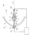
図1は、本発明の一実施例としてのプロジェクター500を示す説明図である。プロジェクター500は、光源装置200と、平行化レンズ305と、照明光学系310と、色分離光学系320と、3つの液晶ライトバルブ330R、330G、330Bと、クロスダイクロイックプリズム340と、投写光学系350とを有している。
1. Optical System of Projector FIG. 1 is an explanatory diagram showing a
光源装置200は、光源ユニット210と、放電灯点灯装置1と、を有している。光源ユニット210は、主反射鏡112と副反射鏡50と放電灯90とを有している。放電灯点灯装置1は、放電灯90に電力を供給して、放電灯90を点灯させる。主反射鏡112は、放電灯90から放出された光を、照射方向Dに向けて反射する。照射方向Dは、光軸AXと平行である。光源ユニット210からの光は、平行化レンズ305を通過して照明光学系310に入射する。この平行化レンズ305は、光源ユニット210からの光を、平行化する。
The
照明光学系310は、光源装置200からの光の照度を液晶ライトバルブ330R、330G、330Bにおいて均一化する。また、照明光学系310は、光源装置200からの光の偏光方向を一方向に揃える。この理由は、光源装置200からの光を液晶ライトバルブ330R、330G、330Bで有効に利用するためである。照度分布と偏光方向とが調整された光は、色分離光学系320に入射する。色分離光学系320は、入射光を、赤(R)、緑(G)、青(B)の3つの色光に分離する。3つの色光は、各色に対応付けられた液晶ライトバルブ330R、330G、330Bによって、それぞれ変調される。液晶ライトバルブ330R、330G、330Bは、液晶パネル560R、560G、560Bと、液晶パネル560R、560G、560Bのそれぞれの光入射側及び出射側に配置される偏光板を備える。変調された3つの色光は、クロスダイクロイックプリズム340によって合成される。合成光は、投写光学系350に入射する。投写光学系350は、入射光を、図示しないスクリーンに投写する。これにより、スクリーン上には画像が表示される。
The illumination optical system 310 makes the illuminance of light from the
なお、平行化レンズ305と、照明光学系310と、色分離光学系320と、クロスダイクロイックプリズム340と、投写光学系350とのそれぞれの構成としては、周知の種々の構成を採用可能である。
Note that various well-known configurations can be adopted as the configurations of the
図2は、光源装置200の構成を示す説明図である。光源装置200は、光源ユニット210と放電灯点灯装置1とを有している。図中には、光源ユニット210の断面図が示されている。光源ユニット210は、主反射鏡112と放電灯90と副反射鏡50とを有している。
FIG. 2 is an explanatory diagram showing the configuration of the
放電灯90の形状は、第1端部90e1から第2端部90e2まで、照射方向Dに沿って延びる棒形状である。放電灯90の材料は、例えば、石英ガラス等の透光性材料である。放電灯90の中央部は球状に膨らんでおり、その内には、放電空間91が形成されている。放電空間91内には、希ガス、金属ハロゲン化合物等を含む放電媒体であるガスが封入されている。
The shape of the
また、放電空間91内には、第1電極92及び第2電極93が、放電灯90から突き出している。第1電極92は、放電空間91の第1端部90e1側に配置され、第2電極93は、放電空間91の第2端部90e2側に配置されている。第1電極92及び第2電極93の形状は、光軸AXに沿って延びる棒形状である。放電空間91内では、第1電極92及び第2電極93の電極先端部(「放電端」とも呼ぶ)が、所定距離だけ離れて向かい合っている。なお、第1電極92及び第2電極93の材料は、例えば、タングステン等の金属である。
In addition, the
放電灯90の第1端部90e1には、第1端子536が設けられている。第1端子536と第1電極92とは、放電灯90の内部を通る導電性部材534によって電気的に接続されている。同様に、放電灯90の第2端部90e2には、第2端子546が設けられている。第2端子546と第2電極93とは、放電灯90の内部を通る導電性部材544によって電気的に接続されている。第1端子536及び第2端子546の材料は、例えば、タングステン等の金属である。また、各導電性部材534、544としては、例えば、モリブデン箔が利用される。
A
第1端子536及び第2端子546は、放電灯点灯装置1に接続されている。放電灯点灯装置1は、第1端子536及び第2端子546に、交流電流を供給する。その結果、第1電極92及び第2電極93の間でアーク放電が起きる。アーク放電により発生した光(放電光)は、破線の矢印で示すように、放電位置から全方向に向かって放射される。
The
放電灯90の第1端部90e1には、固定部材114によって、主反射鏡112が固定されている。主反射鏡112の反射面(放電灯90側の面)の形状は、回転楕円形状である。主反射鏡112は、放電光を照射方向Dに向かって反射する。なお、主反射鏡112の反射面の形状としては、回転楕円形状に限らず、放電光を照射方向Dに向かって反射するような種々の形状を採用可能である。例えば、回転放物線形状を採用してもよい。この場合は、主反射鏡112は、放電光を、光軸AXにほぼ平行な光に変換することができる。したがって、平行化レンズ305を省略することができる。
The main reflecting
放電灯90の第2端部90e2側には、固定部材522によって、副反射鏡50が固定されている。副反射鏡50の反射面(放電灯90側の面)の形状は、放電空間91の第2端部90e2側を囲む球面形状である。副反射鏡50は、放電光を、主反射鏡112に向かって反射する。これにより、放電空間91から放射される光の利用効率を高めることができる。
The
なお、固定部材114、522の材料としては、放電灯90の発熱に耐える任意の耐熱材料(例えば、無機接着剤)を採用可能である。また、主反射鏡112及び副反射鏡50と放電灯90との配置を固定する方法としては、主反射鏡112及び副反射鏡50を放電灯90に固定する方法に限らず、任意の方法を採用可能である。例えば、放電灯90と主反射鏡112とを、独立に、プロジェクターの筐体(図示せず)に固定してもよい。副反射鏡50についても同様である。
As a material for the fixing
2.本実施形態に係る放電灯点灯装置及び放電灯点灯方法
2−1.放電灯点灯装置の構成
図3は、本実施形態に係る放電灯点灯装置1の回路図の一例である。本実施形態に係る放電灯点灯装置1は、電圧パルス印加部10と、交流電圧印加部20と、制御部30とを含んで構成されている。
2. 2. Discharge lamp lighting device and discharge lamp lighting method according to this embodiment 2-1. Configuration of Discharge Lamp Lighting Device FIG. 3 is an example of a circuit diagram of the discharge
電圧パルス印加部10は、第1電極92及び第2電極93を含む放電灯90の第1電極92と第2電極93との間を絶縁破壊するための電圧パルスを第1電極92と第2電極93との間に印加する。すなわち、電圧パルス印加部10は、放電灯90の点灯開始時に放電灯90の電極間を絶縁破壊して放電路を形成するために必要な高電圧(放電灯90の通常点灯時よりも高い電圧)を放電灯90の電極間に供給する。
The voltage
図3に示される例では、電圧パルス印加部10は、ダイオード11と、コンデンサー12と、トランス13と、スイッチ素子14とを含んで構成されている。スイッチ素子14は、例えばトランジスターで構成されていてもよい。図3に示される例では、ダイオード11のアノード端子は、トランス13の2次側巻線L2を介して放電灯90の第1電極92と接続されるように構成されている。また、ダイオード11のカソード端子は、トランス13の1次側巻線L1とスイッチ素子14とを介して放電灯90の第2電極93と接続されるとともに、コンデンサー12を介して放電灯90の第2電極93と接続されるように構成されている。また、スイッチ素子14の制御端子には制御部30から電圧パルス印加制御信号S1が入力されてスイッチ素子14のON/OFF状態が制御される。
In the example shown in FIG. 3, the voltage
図3に示される電圧パルス印加部10では、以下の動作によって電圧パルスが発生する。まずスイッチ素子14をOFF状態として、ダイオード11を介してコンデンサー12に電荷を蓄積する。次にスイッチ素子14をON状態とすることでコンデンサー12及びトランス13の1次側巻線L1とで直列共振回路が形成される。これによって、コンデンサー12に蓄積された電荷がトランス13の1次側巻線L1に流れこみ、トランス13の2次側巻線L2に高電圧の減衰振動となる電圧パルスが発生する。発生した電圧パルスが放電灯90の第1電極92と第2電極93との間に印加されることによって、第1電極92と第2電極93との間が絶縁破壊される。
In the voltage
交流電圧印加部20は、第1電極92が陽極となる第1極性期間と第2電極93が陽極となる第2極性期間を含む交流電圧を放電灯90に印加する。図3に示される例では、交流電圧印加部20は、電力生成回路22と極性反転回路24とを含んで構成されている。
The AC
電力生成回路22は、放電灯90に供給する駆動電力を生成する。図3に示される例では、電力生成回路22は、直流電源80を入力とし、当該入力電圧を降圧するダウンチョッパー回路で構成されている。また、電力生成回路22は、直流電流Idを出力する。
The
図3に示される例では、電力生成回路22は、スイッチ素子221、ダイオード222、コイル223及びコンデンサー224を含んで構成されている。スイッチ素子221は、例えばトランジスターで構成されていてもよい。図3に示される例では、スイッチ素子221の一端は直流電源80の正電圧側に接続され、他端はダイオード222のカソード端子及びコイル223の一端に接続されている。また、コイル223の他端にはコンデンサー224の一端が接続され、コンデンサー224の他端はダイオード222のアノード端子及び直流電源80の負電圧側に接続されている。スイッチ素子221の制御端子には制御部30から電力制御信号S2が入力されてスイッチ素子221のON/OFF状態が制御される。電力制御信号S2には、例えばPWM(Pulse Width Modulation)制御信号が用いられてもよい。
In the example illustrated in FIG. 3, the
電力生成回路22において、スイッチ素子221をON状態とすると、コイル223に電流が流れ、コイル223にエネルギーが蓄えられる。その後、スイッチ素子221をOFF状態とすると、コイル223に蓄えられたエネルギーがコンデンサー224とダイオード222とを通る経路で放出される。その結果、スイッチ素子221をON状態とする時間の割合に応じた直流電流Idが発生する。
In the
極性反転回路24は、電力生成回路22から出力される直流電流Idを入力し、所与のタイミングで極性反転することにより、放電灯90の第1電極92と第2電極93との間に交流電圧を印加する。また、極性反転回路24は、制御された時間だけ継続する直流であったり、任意の周波数をもつ交流であったりする駆動電流Iを生成出力する。本実施形態においては、極性反転回路24はインバーターブリッジ回路(フルブリッジ回路)で構成されている。
The
図3に示される例では、極性反転回路24は、4つのスイッチ素子241〜244を含んで構成されている。極性反転回路24は、直列接続されたスイッチ素子241及びスイッチ素子242と、直列接続されたスイッチ素子243及び244とを、互いに並列接続して構成されている。スイッチ素子241〜244の制御端子には、それぞれ制御部30から極性反転制御信号C1〜C4が入力され、スイッチ素子241〜244のON/OFF状態が制御される。
In the example shown in FIG. 3, the
極性反転回路24は、スイッチ素子241及びスイッチ素子244と、スイッチ素子242及びスイッチ素子243を交互にON/OFFを繰り返すことにより、電力生成回路22から出力される直流電流Idの極性を交互に反転し、スイッチ素子241及びスイッチ素子242の共通接続点とスイッチ素子243及びスイッチ素子244の共通接続点との間に交流電圧を発生させる。
The
すなわち、スイッチ素子241及びスイッチ素子244がON状態の時にはスイッチ素子242及びスイッチ素子243をOFF状態とし、スイッチ素子241及びスイッチ素子244がOFF状態の時にはスイッチ素子242及びスイッチ素子243をON状態となるように制御する。したがって、スイッチ素子241及びスイッチ素子244がON状態の時には、コンデンサー224の一端からスイッチ素子241、放電灯90、スイッチ素子244の順に流れる駆動電流Iが発生する。また、スイッチ素子242及びスイッチ素子243がON状態の時には、コンデンサー224の一端からスイッチ素子243、放電灯90、スイッチ素子242の順に流れる駆動電流Iが発生する。
That, the ON state the
制御部30は、電圧パルス印加部10及び交流電圧印加部20を制御する。図3に示される例では、制御部30は、電圧パルス印加制御手段31、電力制御手段32及び極性反転制御手段33を含んで構成されている。
The
電圧パルス印加制御手段31は、電圧パルス印加部10のスイッチ素子14に電圧パルス印加制御信号S1を出力することによって電圧パルス印加部10を制御する。
The voltage pulse application control means 31 controls the voltage
電力制御手段32は、電力生成回路22のスイッチ素子221に電力制御信号S2を出力することによって電力生成回路22を制御する。
The
極性反転制御手段33は、極性反転回路24のスイッチ素子241〜244に極性反転制御信号C1〜C4を出力することによって極性反転回路24を制御する。
The polarity inversion control means 33 controls the
なお、制御部30は、その一部又は全てを半導体集積回路で構成してもよい。また、制御部30は、専用回路により実現して前述された制御や後述される処理の各種制御を行うようにすることもできるが、例えばCPU(Central Processing Unit)が記憶部(不図示)に記憶された制御プログラムを実行することによりコンピューターとして機能し、これらの処理の各種制御を行うようにすることもできる。
Note that a part or all of the
放電灯点灯装置1は、電流測定用の抵抗40を含んでいてもよい。図3に示される例では、抵抗40は、放電灯90と直列に接続されるように構成されている。抵抗40の両端に発生する電位差を測定することによって、放電灯90の駆動電流Iを測定することができる。
The discharge
放電灯点灯装置1は、電圧検出手段34を含んで構成されていてもよい。図3に示される例では、電圧検出手段34は、制御部30の一部として構成されている。また、電圧検出手段34は、ダイオード11のアノード端子の電位V1と、抵抗40の両端の電位V2及びV3を検出している。電位V1と電位V3との差によって放電灯90の駆動電圧Vlaを測定することができる。また、電位V2と電位V3との差によって放電灯90の駆動電流Iを測定することができる。
The discharge
2−2.グロー放電からアーク放電までの電極の状態
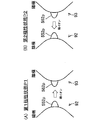
図4(A)は、第1電極92が陽極となる第1極性状態P1を説明するための図、図4(B)は第2電極93が陽極となる第2極性状態P2を説明するための図である。図4(A)及び図4(B)には、第1電極92及び第2電極93の先端部分が示されている。第1電極92の先端には突起552pが、第2電極93の先端には突起562pがそれぞれ設けられている。放電は、これらの突起552p、562pの間で生じる。第1電極92及び第2電極93の先端に突起を設けることによって、突起が無い場合と比べて、第1電極92及び第2電極93における放電位置(アーク位置)の移動を抑えることができる。ただし、このような突起を省略してもよい。
2-2. FIG. 4A is a diagram for explaining the first polarity state P1 in which the
図4(A)は、第1電極92が陽極として動作し、第2電極93が陰極として動作する第1極性状態P1を示している。電圧パルス印加部10によって第1電極92と第2電極93との間が絶縁破壊された後の第1極性状態P1では、グロー放電によって、第1電極92(陽極)から第2電極93(陰極)へ陽イオン(放電灯90に封入されている放電媒体であるガスに含まれる金属イオンなど)が移動し、第2電極93(陰極)の先端に衝突する。陽イオンの衝突によって、第2電極93(陰極)の材料(タングステンなど)の一部が削り取られるスパッタリングが発生する。また、陽イオンの衝突によって熱が生じ、第2電極93(陰極)の先端の温度が上昇する。第2電極93(陰極)の温度が上がり、第2電極93(陰極)から熱電子放出が始まることで、グロー放電からアーク放電へと移行する。
FIG. 4A shows a first polarity state P1 in which the
図4(B)は、第2電極93が陽極として動作し、第1電極92が陰極として動作する第2極性状態P2を示している。電圧パルス印加部10によって第2電極93と第1電極92との間が絶縁破壊された後の第2極性状態P2では、グロー放電によって、第2電極93(陽極)から第1電極92(陰極)へ陽イオンが移動し、第1電極92(陰極)の先端に衝突する。陽イオンの衝突によって、第1電極92(陰極)の材料の一部が削り取られるスパッタリングが発生する。また、陽イオンの衝突によって熱が生じ、第1電極92(陰極)の先端の温度が上昇する。第1電極92(陰極)の温度が上がり、第1電極92(陰極)から熱電子放出が始まることで、グロー放電からアーク放電へと移行する。
FIG. 4B shows a second polarity state P2 in which the
2−3.放電灯点灯方法、及び、放電灯点灯装置の制御例
図5は、本実施形態に係る放電灯点灯方法を説明するためのフローチャートである。
2-3. Example of Control of Discharge Lamp Lighting Method and Discharge Lamp Lighting Device FIG. 5 is a flowchart for explaining the discharge lamp lighting method according to the present embodiment.
本実施形態に係る放電灯点灯方法は、第1電極92及び第2電極93を含む放電灯90を点灯させる放電灯点灯方法であって、第1電極92と第2電極93との間を絶縁破壊する絶縁破壊工程(ステップS100)と、絶縁破壊工程(ステップS100)の後に、第1電極92が陽極となる第1極性期間が、第2電極93が陽極となる第2極性期間よりも長い交流電圧を放電灯90に印加する第1工程(ステップS102)と、第1工程(ステップS102)の後に、第2極性期間が第1極性期間よりも長い交流電圧を放電灯90に印加する第2工程(ステップS104)と、を含む。
The discharge lamp lighting method according to the present embodiment is a discharge lamp lighting method for lighting a
以下では、放電灯点灯装置1を用いて本実施形態に係る放電灯点灯方法を実現するための放電灯点灯装置1の制御例について説明する。
Below, the control example of the discharge
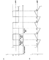
図6(A)は、第1電極92と第2電極93との間に印加される電圧Vのタイミングチャート、図6(B)は、駆動電流Iのタイミングチャートである。図6(A)の横軸は時間、縦軸は第1電極92と第2電極93との間に印加される電圧Vを表す。図6(B)の横軸は時間、縦軸は駆動電流Iを表す。また、図6(A)及び図6(B)において、後述される電圧パルス印加処理が行われる期間を電圧パルス印加期間、後述される第1制御処理が行われる期間を第1制御処理期間とする。
6A is a timing chart of the voltage V applied between the
図5のフローチャートに示されるように、本実施形態に係る放電灯点灯方法は、まず、絶縁破壊工程(ステップS100)を行う。放電灯点灯装置1においては、制御部30が、電圧パルス印加部10によって、第1電極92と第2電極93との間に電圧パルスを印加させる電圧パルス印加処理を行う。
As shown in the flowchart of FIG. 5, in the discharge lamp lighting method according to the present embodiment, first, a dielectric breakdown process (step S100) is performed. In the discharge
電圧パルス印加処理において、制御部30は、まず、極性反転制御手段33によって、スイッチ素子241及びスイッチ素子244をOFF状態、スイッチ素子242及びスイッチ素子243をON状態とし、電圧パルス印加制御手段31によって、スイッチ素子14をOFF状態とする。これによって、コンデンサー12に電荷が蓄えられる。次に、制御部30は、図6(A)における時刻t0において、電圧パルス印加制御手段31によって、スイッチ素子14をON状態とする。これによって、図6(A)の電圧パルス印加期間に示される高電圧の電圧パルスが第1電極92と第2電極93との間に印加される。これによって、第1電極92と第2電極93との間を絶縁破壊する。
In the voltage pulse application process, the
図5のフローチャートに示されるように、本実施形態に係る放電灯点灯方法は、絶縁破壊工程(ステップS100)の後に、第1電極92が陽極となる第1極性期間が、第2電極93が陽極となる第2極性期間よりも長い交流電圧を放電灯90に印加する第1工程(ステップS102)を行う。放電灯点灯装置1においては、制御部30が、電圧パルス印加処理を行った後に、交流電圧印加部20によって、第1極性期間が第2極性期間よりも長い交流電圧を放電灯90に印加させる第1制御処理を行う。
As shown in the flowchart of FIG. 5, in the discharge lamp lighting method according to the present embodiment, after the dielectric breakdown step (step S100), the first polarity period in which the
第1極性期間において、制御部30は、電力制御手段32によって電力生成回路22の出力電圧の値をEで一定となるように制御した状態で、極性反転制御手段33によって、スイッチ素子241及びスイッチ素子244をOFF状態、スイッチ素子242及びスイッチ素子243をON状態とする。第2極性期間において、制御部30は、電力制御手段32によって電力生成回路22の出力電圧の値をEで一定となるように制御した状態で、極性反転制御手段33によって、スイッチ素子241及びスイッチ素子244をON状態、スイッチ素子242及びスイッチ素子243をOFF状態とする。極性反転制御手段33がスイッチ素子241〜244の状態を切り替えるタイミングを制御することによって、交流電圧印加部20によって、第1極性期間が第2極性期間よりも長い交流電圧を放電灯90に印加させることができる。
In the first polarity period, the
図6(A)に示される例では、時刻t1から時刻t2まで、時刻t3から時刻t4まで、時刻t5から時刻t6まで、時刻t7から時刻t8までが第2極性期間、時刻t2から時刻t3まで、時刻t4から時刻t5まで、時刻t6から時刻t7まで、時刻t8から時刻t9までが第1極性期間となっている。 In the example shown in FIG. 6A, the second polarity period is from time t1 to time t2, from time t3 to time t4, from time t5 to time t6, from time t7 to time t8, and from time t2 to time t3. The first polarity period is from time t4 to time t5, from time t6 to time t7, and from time t8 to time t9.
また、図6(A)に示される例では、第1極性期間の長さは第2極性期間の長さの4倍程度となっている。なお、第1極性期間の長さ及び第2極性期間の長さは、放電灯90の仕様に応じて実験的に決定することができる。
In the example shown in FIG. 6A, the length of the first polarity period is about four times the length of the second polarity period. Note that the length of the first polarity period and the length of the second polarity period can be determined experimentally according to the specifications of the
図6(B)に示されるように、駆動電流Iは、第1極性期間と第2極性期間とで逆向きの電流となる。図6(B)に示される例では、第1極性期間においても第2極性期間においても、時間とともに駆動電流Iの絶対値が増加している。本実施形態に係る放電灯点灯装置1においては、トランス13の2次側巻線L2の影響によって、電圧Vの変化よりも遅れて駆動電流Iが変化するからである。
As shown in FIG. 6B, the drive current I is a reverse current in the first polarity period and the second polarity period. In the example shown in FIG. 6B, the absolute value of the drive current I increases with time in both the first polarity period and the second polarity period. This is because in the discharge
また、図6(B)に示されるように、第1極性期間における駆動電流Iの絶対値の最大値は、時間的に後の第1極性期間ほど大きくなっている。「2−2.グロー放電からアーク放電までの電極の状態」の項で説明したとおり、第1極性期間では第2電極93の温度が上がり、第2電極93から熱電子の放出が始まるため、駆動電流Iは大きくなる。
In addition, as shown in FIG. 6B, the maximum value of the absolute value of the drive current I in the first polarity period is larger in the first polarity period later in time. As described in the section “2-2. Electrode State from Glow Discharge to Arc Discharge”, the temperature of the
一方、図6(B)に示されるように、第2極性期間の長さは短いため、第2極性期間における駆動電流Iの絶対値の最大値は大きく変化していない。 On the other hand, as shown in FIG. 6B, since the length of the second polarity period is short, the maximum absolute value of the drive current I in the second polarity period does not change significantly.
すなわち、第1制御処理においては、第2電極93を積極的に温めるように制御することによって、第2電極93からの放電を速やかにグロー放電からアーク放電へと移行させている。また、第2極性期間の長さは短いため、スパッタリングによる悪影響は小さい。
That is, in the first control process, the discharge from the
図7(A)は、図6(A)で示されるタイミングチャートの後の第1電極92と第2電極93との間に印加される電圧Vのタイミングチャート、図7(B)は、図6(B)で示されるタイミングチャートの後の駆動電流Iのタイミングチャートである。図7(A)の横軸は時間、縦軸は第1電極92と第2電極93との間に印加される電圧Vを表す。図7(B)の横軸は時間、縦軸は駆動電流Iを表す。また、図7(A)及び図7(B)において、後述される第2制御処理が行われる期間を第2制御処理期間とする。
7A is a timing chart of the voltage V applied between the
図5のフローチャートに示されるように、本実施形態に係る放電灯点灯方法は、第1工程(ステップS102)の後に、第2極性期間が第1極性期間よりも長い交流電圧を放電灯90に印加する第2工程(ステップS104)を行う。放電灯点灯装置1においては、制御部30が、第1制御処理を行った後に、交流電圧印加部20によって、第2極性期間が第1極性期間よりも長い交流電圧を放電灯90に印加させる第2制御処理を行う。
As shown in the flowchart of FIG. 5, in the discharge lamp lighting method according to the present embodiment, after the first step (step S102), an AC voltage having a second polarity period longer than the first polarity period is applied to the
本実施形態に係る放電灯点灯装置1においては、極性反転制御手段33がスイッチ素子241〜244の状態を切り替えるタイミングを制御することによって、交流電圧印加部20によって、第2極性期間の長さがが第1極性期間の長さよりも長い交流電圧を放電灯90に印加させることができる。
In the discharge
図7(A)に示される例では、時刻t11から時刻t12まで、時刻t13から時刻t14まで、時刻t15から時刻t16までが第2極性期間、時刻t12から時刻t13まで、時刻t14から時刻t15まで、時刻t16から時刻t17までが第1極性期間となっている。 In the example shown in FIG. 7A, from time t11 to time t12, from time t13 to time t14, from time t15 to time t16 is the second polarity period, from time t12 to time t13, from time t14 to time t15. From time t16 to time t17 is the first polarity period.
また、図7(A)に示される例では、第2極性期間の長さは第1極性期間の長さの3倍程度となっている。なお、第1極性期間の長さ及び第2極性期間の長さは、放電灯90の仕様に応じて実験的に決定することができる。
In the example shown in FIG. 7A, the length of the second polarity period is about three times the length of the first polarity period. Note that the length of the first polarity period and the length of the second polarity period can be determined experimentally according to the specifications of the
図7(B)に示されるように、第2極性期間における駆動電流Iの絶対値の最大値は、時間的に後の第2極性期間ほど大きくなっている。「2−2.グロー放電からアーク放電までの電極の状態」の項で説明したとおり、第2極性期間では第1電極92の温度が上がり、第1電極92から熱電子の放出が始まるため、駆動電流Iは大きくなる。
As shown in FIG. 7B, the maximum value of the absolute value of the drive current I in the second polarity period is larger in the second polarity period later in time. As described in the section “2-2. Electrode State from Glow Discharge to Arc Discharge”, the temperature of the
一方、図7(B)に示されるように、第1極性期間の長さは短いため、第1極性期間における駆動電流Iの絶対値の最大値は大きく変化していない。 On the other hand, as shown in FIG. 7B, since the length of the first polarity period is short, the maximum value of the absolute value of the driving current I in the first polarity period does not change greatly.
すなわち、第2制御処理においては、第1電極92を積極的に温めるように制御することによって、第1電極92からの放電を速やかにグロー放電からアーク放電へと移行させている。
That is, in the second control process, the discharge from the
本実施形態に係る放電灯点灯装置1によれば、第1制御処理によって陰極となる第2電極93からの放電を速やかにグロー放電からアーク放電へと移行させ、第2制御処理によって陰極となる第1電極92からの放電を速やかにグロー放電からアーク放電へと移行させることで、第1電極92と第2電極93とに対称的な交流電圧を印加する場合に比べてグロー放電となる期間を短くすることができる。したがって、スパッタリングによる放電灯90の黒化現象を抑制できる放電灯点灯装置を実現できる。
According to the discharge
また、本実施形態に係る放電灯点灯方法によれば、第1工程では陰極となる第2電極93からの放電を速やかにグロー放電からアーク放電へと移行させ、第2工程では陰極となる第1電極92からの放電を速やかにグロー放電からアーク放電へと移行させることで、グロー放電となる期間を短くすることができる。したがって、スパッタリングによる放電灯の黒化現象を抑制できる放電灯点灯方法を実現できる。
In addition, according to the discharge lamp lighting method according to the present embodiment, the discharge from the
なお、放電灯90のうち、より温まりやすい電極を第2電極93とすることが好ましい。例えば、図2に示されるような光源装置200の場合には、主反射鏡112に近い側の電極よりも主反射鏡から遠い側の電極の方が、実質的な熱容量が小さくなるので温まりやすい。したがって、本実施形態においても、主反射鏡112に近い側を第1電極92とし、主反射鏡112から遠い側を第2電極93としている。より温まりやすい電極を第1工程で加熱することにより、より速やかにアーク放電へと移行させることができる。
In addition, it is preferable that the electrode which is more easily heated among the
本実施形態に係る放電灯点灯方法において、第2工程(ステップS104)における第2極性期間の長さに対する第1極性期間の長さの比が、第1工程(ステップS102)における第1極性期間の長さに対する第2極性期間の長さの比よりも大きくなるように、第1工程(ステップS102)及び第2工程(ステップS104)を行ってもよい。本実施形態に係る放電灯点灯装置1においては、制御部30が、第2制御処理における第2極性期間の長さに対する第1極性期間の長さの比が、第1制御処理における第1極性期間の長さに対する第2極性期間の長さの比よりも大きくなるように、第1制御処理及び第2制御処理を行ってもよい。
In the discharge lamp lighting method according to the present embodiment, the ratio of the length of the first polarity period to the length of the second polarity period in the second step (step S104) is the first polarity period in the first step (step S102). The first step (step S102) and the second step (step S104) may be performed so as to be larger than the ratio of the length of the second polarity period to the length of. In the discharge
図6(B)及び図7(B)に示される例では、第2制御処理における第2極性期間の長さに対する第1極性期間の長さの比は1/3、第1制御処理における第1極性期間の長さに対する第2極性期間の長さの比は1/4となっている。 In the example shown in FIGS. 6B and 7B, the ratio of the length of the first polarity period to the length of the second polarity period in the second control process is 1/3, and the first control process has the first ratio. The ratio of the length of the second polarity period to the length of the one polarity period is 1/4.
制御部30がこのような制御を行うことによって、第1制御処理によっては第2電極93を速やかに加熱でき、第2制御処理によっては第1制御処理で加熱された第2電極93の温度が下がることを抑制しつつ第1電極92を加熱できる。したがって、第1電極92及び第2電極93の両方を速やかに加熱できるので、スパッタリングによる放電灯の黒化現象を抑制できる放電灯点灯装置を実現できる。
When the
本実施形態に係る放電灯点灯方法において、第2工程(ステップS104)の後に、第1極性期間の長さと第2極性期間の長さとが等しい交流電圧を放電灯に印加する第3工程をさらに行ってもよい。本実施形態に係る放電灯点灯装置1においては、制御部30が、第2制御処理の後に、交流電圧印加部20によって、第1極性期間の長さと第2極性期間の長さとが等しい交流電圧を放電灯90に印加させる第3制御処理をさらに行ってもよい。
In the discharge lamp lighting method according to the present embodiment, after the second step (step S104), a third step of applying an AC voltage having the same length of the first polarity period and the length of the second polarity period to the discharge lamp is further performed. You may go. In the discharge
図8(A)は、図7(A)で示されるタイミングチャートの後の第1電極92と第2電極93との間に印加される電圧Vのタイミングチャート、図8(B)は、図7(B)で示されるタイミングチャートの後の駆動電流Iのタイミングチャートである。図8(A)の横軸は時間、縦軸は第1電極92と第2電極93との間に印加される電圧Vを表す。図8(B)の横軸は時間、縦軸は駆動電流Iを表す。
8A is a timing chart of the voltage V applied between the
本実施形態に係る放電灯点灯装置1においては、極性反転制御手段33がスイッチ素子241〜244の状態を切り替えるタイミングを制御することによって、交流電圧印加部20によって、第1極性期間の長さと第2極性期間の長さとが等しい交流電圧を放電灯90に印加させることができる。
In the discharge
図8(A)に示される例では、時刻t21から時刻t22まで、時刻t23から時刻t24まで、時刻t25から時刻t26までが第2極性期間、時刻t22から時刻t23まで、時刻t24から時刻t25まで、時刻t26から時刻t27までが第1極性期間となっている。なお、第1極性期間の長さ及び第2極性期間の長さは、放電灯90の仕様に応じて実験的に決定することができる。
In the example shown in FIG. 8A, the second polarity period is from time t21 to time t22, from time t23 to time t24, from time t25 to time t26, from time t22 to time t23, from time t24 to time t25. The time period from time t26 to time t27 is the first polarity period. Note that the length of the first polarity period and the length of the second polarity period can be determined experimentally according to the specifications of the
図8(B)に示されるように、第1極性期間における駆動電流Iの絶対値の最大値と第2極性期間における駆動電流Iの絶対値の最大値は同程度となっている。 As shown in FIG. 8B, the maximum value of the absolute value of the drive current I in the first polarity period and the maximum value of the absolute value of the drive current I in the second polarity period are approximately the same.
制御部30が第3制御処理を行うことによって、放電灯90の一方の電極が他方の電極よりも消耗することを抑制できる。
When the
2−4.放電灯点灯方法、及び、放電灯点灯装置の制御例の変形例
本実施形態に係る放電灯点灯方法は、第1工程(ステップS102)及び第2工程(ステップS104)において、第1極性期間と第2極性期間との間に、第1電極92及び第2電極93のいずれも陽極とならない期間を有する交流電圧を印加してもよい。本実施形態に係る放電灯点灯装置1においては、制御部30が、第1制御処理及び第2制御処理において、交流電圧印加部20によって、第1極性期間と第2極性期間との間に、第1電極及び第2電極のいずれも陽極とならない期間を有する交流電圧を印加させてもよい。
2-4. Modified example of discharge lamp lighting method and control example of discharge lamp lighting device The discharge lamp lighting method according to the present embodiment includes a first polarity period in the first step (step S102) and the second step (step S104). You may apply the alternating voltage which has a period when neither the
図9は、変形例における第1電極92と第2電極93との間に印加される電圧Vのタイミングチャートである。図9の横軸は時間、縦軸は第1電極92と第2電極93との間に印加される電圧Vを表す。
FIG. 9 is a timing chart of the voltage V applied between the
図9に示される例では、第1制御期間及び第2制御期間において、第2極性期間と、第2極性期間の後の第1極性期間との間に、第1電極及び第2電極のいずれも陽極とならない無極性期間を有している。なお、図9には示されていないが、第1制御期間及び第2制御期間において、第1極性期間と、第1極性期間の後の第2極性期間との間にも、第1電極及び第2電極のいずれも陽極とならない無極性期間を有している。また、図9に示されるように、制御部30は、第3制御期間においても、第1極性期間と第2極性期間との間に無極性期間を有するように交流電圧印加部20を制御してもよい。
In the example shown in FIG. 9, in the first control period and the second control period, any of the first electrode and the second electrode is between the second polarity period and the first polarity period after the second polarity period. Also has a nonpolar period during which it does not become an anode. Although not shown in FIG. 9, in the first control period and the second control period, the first electrode and the second polarity period between the first polarity period and the second polarity period after the first polarity period are also included. None of the second electrodes has a nonpolar period during which it does not become an anode. Further, as shown in FIG. 9, the
無極性期間において、制御部30は、極性反転制御手段33によって、スイッチ素子241〜244をOFF状態とする。
In the non-polar period, the
制御部30が、無極性期間を有するように交流電圧印加部20を制御することによって、交流電圧の周期を変えずに第1極性期間と第2極性期間の長さを独立に設計できる自由度を大きくすることができる。また、極性反転回路24において、スイッチ素子241及びスイッチ素子242を貫通する貫通電流や、スイッチ素子243及びスイッチ素子244を貫通する貫通電流が流れるリスクを低減できる。
The degree of freedom in which the
3.プロジェクターの回路構成
図10は、本実施の形態に係るプロジェクターの回路構成の一例を示す図である。プロジェクター500は、先に説明した光学系の他に、画像信号変換部510、直流電源装置80、液晶パネル560R、560G、560B、画像処理装置570を含む。
3. FIG. 10 is a diagram illustrating an example of a circuit configuration of the projector according to the present embodiment. The
画像信号変換部510は、外部から入力された画像信号502(輝度−色差信号やアナログRGB信号など)を所定のワード長のデジタルRGB信号に変換して画像信号512R、512G、512Bを生成し、画像処理装置570に供給する。
The
画像処理装置570は、3つの画像信号512R、512G、512Bに対してそれぞれ画像処理を行い、液晶パネル560R、560G、560Bをそれぞれ駆動するための駆動信号572R、572G、572Bを出力する。
The
直流電源装置520は、外部の交流電源600から供給される交流電圧を一定の直流電圧に変換し、トランス(図示しないが、直流電源装置520に含まれる)の2次側にある画像信号変換部510、画像処理装置570及びトランスの1次側にある放電灯点灯装置1に直流電圧を供給する。
The DC power supply device 520 converts an AC voltage supplied from an external
液晶パネル560R、560G、560Bは、それぞれ駆動信号572R、572G、572Bにより、先に説明した光学系を介して各液晶パネルに入射する色光の輝度を変調する。
The
CPU(Central Processing Unit)580は、プロジェクターの点灯開始から消灯に至るまでの動作を制御する。例えば、点灯命令や消灯命令を、通信信号582を介して放電灯点灯装置1に出力してもよい。また、CPU580は、放電灯点灯装置1から放電灯90の点灯の有無に関する情報を、通信信号532を介して受け取ってもよい。
A CPU (Central Processing Unit) 580 controls operations from the start of lighting of the projector to the extinction thereof. For example, a lighting command or a lighting command may be output to the discharge
放電灯点灯装置1は、起動時に放電灯90の電極間に高電圧を発生して絶縁破壊させて放電路を形成し、以後放電灯90が放電を維持するための駆動電流Iを供給する。放電灯点灯装置の詳細については、「2.本実施形態に係る放電灯点灯装置及び放電灯点灯方法」の項で述べたとおりである。
The discharge
このように構成したプロジェクター500は、スパッタリングによる放電灯の黒化現象を抑制できる放電灯点灯装置1を含むので、放電灯90を長期間使用できるプロジェクターを実現できる。
Since the
上記各実施形態においては、3つの液晶パネルを用いたプロジェクターを例示して説明したが、本発明はこれに限定されるものではなく、1つ、2つ又は4つ以上の液晶パネルを用いたプロジェクターにも適用可能である。 In each of the above embodiments, a projector using three liquid crystal panels has been described as an example. However, the present invention is not limited to this, and one, two, four or more liquid crystal panels are used. It can also be applied to projectors.
上記各実施形態においては、透過型のプロジェクターを例示して説明したが、本発明はこれに限定されるものではなく、反射型のプロジェクターにも適用することが可能である。ここで、「透過型」とは、透過型の液晶パネル等のように光変調手段としての電気光学変調装置が光を透過するタイプであることを意味しており、「反射型」とは、反射型の液晶パネルやマイクロミラー型光変調装置などのように光変調手段としての電気光学変調装置が光を反射するタイプであることを意味している。マイクロミラー型光変調装置としては、例えば、DMD(デジタルマイクロミラーデバイス;Texas Instruments社の商標)を用いることができる。反射型のプロジェクターにこの発明を適用した場合にも、透過型のプロジェクターと同様の効果を得ることができる。 In each of the above embodiments, a transmissive projector has been described as an example. However, the present invention is not limited to this, and can be applied to a reflective projector. Here, “transmission type” means that an electro-optic modulation device as a light modulation means such as a transmission type liquid crystal panel transmits light, and “reflection type” means This means that an electro-optic modulator as a light modulator such as a reflective liquid crystal panel or a micromirror type light modulator is a type that reflects light. As the micromirror light modulator, for example, DMD (digital micromirror device; trademark of Texas Instruments) can be used. Even when the present invention is applied to a reflective projector, the same effect as that of a transmissive projector can be obtained.
本発明は、投写画像を観察する側から投写するフロント投写型プロジェクターに適用する場合にも、投写画像を観察する側とは反対の側から投写するリア投写型プロジェクターに適用する場合にも可能である。 The present invention can be applied to a front projection type projector that projects from the side that observes the projected image, or to a rear projection type projector that projects from the side opposite to the side that observes the projected image. is there.
なお、本発明は上述の実施形態に限定されず、本発明の要旨の範囲内で種々の変形実施が可能である。 In addition, this invention is not limited to the above-mentioned embodiment, A various deformation | transformation implementation is possible within the range of the summary of this invention.
本発明は、実施の形態で説明した構成と実質的に同一の構成(例えば、機能、方法及び結果が同一の構成、あるいは目的及び効果が同一の構成)を含む。また、本発明は、実施の形態で説明した構成の本質的でない部分を置き換えた構成を含む。また、本発明は、実施の形態で説明した構成と同一の作用効果を奏する構成又は同一の目的を達成することができる構成を含む。また、本発明は、実施の形態で説明した構成に公知技術を付加した構成を含む。 The present invention includes configurations that are substantially the same as the configurations described in the embodiments (for example, configurations that have the same functions, methods, and results, or configurations that have the same objects and effects). In addition, the invention includes a configuration in which a non-essential part of the configuration described in the embodiment is replaced. In addition, the present invention includes a configuration that exhibits the same operational effects as the configuration described in the embodiment or a configuration that can achieve the same object. Further, the invention includes a configuration in which a known technique is added to the configuration described in the embodiment.
1 放電灯点灯装置、10 電圧パルス印加部、11 ダイオード、12 コンデンサー、13 トランス、14 スイッチ素子、20 交流電圧印加部、22 電力生成回路、24 極性反転回路、30 制御部、31 電圧パルス印加制御手段、32 電力制御手段、33 極性反転制御手段、34 電圧検出手段、40 抵抗、50 副反射鏡、80 直流電源、90 放電灯、91 放電空間、92 第1電極、93 第2電極、112 主反射鏡、114 固定部材、200 光源装置、210 光源ユニット、221 スイッチ素子、222 ダイオード、223 コイル、224 コンデンサー、241〜244 スイッチ素子、305 平行化レンズ、310 照明光学系、320 色分離光学系、330R,330G,330B 液晶ライトバルブ、340 クロスダイクロイックプリズム、350 投写光学系、500 プロジェクター、502 画像信号、510 画像信号変換部、512R 画像信号(R)、512G 画像信号(G)、512B 画像信号(B)、522 固定部材、532 通信信号、534 導電性部材、536 第1端子、544 導電性部材、546 第2端子、552p 突起、560G 液晶パネル(G)、560B 液晶パネル(B)、562p 突起、570 画像処理装置、572R 液晶パネル(R)駆動信号、572G 液晶パネル(G)駆動信号、572B 液晶パネル(B)駆動信号、580 CPU、582 通信信号、600 交流電源、700 スクリーン、C1〜C4 極性反転制御信号、L1 1次側巻線、L2 2次側巻線、S1 電圧パルス印加制御信号、S2 電力制御信号 DESCRIPTION OF SYMBOLS 1 Discharge lamp lighting device, 10 Voltage pulse application part, 11 Diode, 12 Capacitor, 13 Transformer, 14 Switch element, 20 AC voltage application part, 22 Power generation circuit, 24 Polarity inversion circuit, 30 Control part, 31 Voltage pulse application control Means, 32 power control means, 33 polarity inversion control means, 34 voltage detection means, 40 resistance, 50 sub-reflection mirror, 80 DC power supply, 90 discharge lamp, 91 discharge space, 92 first electrode, 93 second electrode, 112 main Reflector, 114 fixing member, 200 light source device, 210 light source unit, 221 switch element, 222 diode, 223 coil, 224 condenser, 241 to 244 switch element, 305 collimating lens, 310 illumination optical system, 320 color separation optical system, 330R, 330G, 330B Liquid crystal light valve 340 Cross dichroic prism, 350 projection optical system, 500 projector, 502 image signal, 510 image signal converter, 512R image signal (R), 512G image signal (G), 512B image signal (B), 522 fixing member, 532 Communication signal 534 Conductive member 536 First terminal 544 Conductive member 546 Second terminal 552p Protrusion 560G Liquid crystal panel (G) 560B Liquid crystal panel (B) 562p Protrusion 570 Image processing device 572R Liquid crystal Panel (R) drive signal, 572G Liquid crystal panel (G) drive signal, 572B Liquid crystal panel (B) drive signal, 580 CPU, 582 communication signal, 600 AC power supply, 700 screen, C1-C4 polarity inversion control signal, L1 primary Side winding, L2 Secondary winding, S1 Voltage pulse Application control signal, S2 power control signal
Claims (6)
前記第1電極が陽極となる第1極性期間と前記第2電極が陽極となる第2極性期間を含む交流電圧を前記放電灯に印加する交流電圧印加部と、
前記電圧パルス印加部及び前記交流電圧印加部を制御する制御部と、
を含み、
前記制御部は、前記放電灯をグロー放電からアーク放電へと移行させる際に、
前記電圧パルス印加部によって、前記第1電極と前記第2電極との間に前記電圧パルスを印加させる電圧パルス印加処理と、
前記電圧パルス印加処理を行った後に、前記交流電圧印加部によって、前記第1極性期間の長さが前記第2極性期間の長さよりも長い前記交流電圧を前記放電灯に印加させる第1制御処理と、
前記第1制御処理を行った後に、前記交流電圧印加部によって、前記第2極性期間の長さが前記第1極性期間の長さよりも長い前記交流電圧を前記放電灯に印加させる第2制御処理と、
を行う、放電灯点灯装置。 A voltage pulse for applying a voltage pulse between the first electrode and the second electrode for dielectric breakdown between the first electrode and the second electrode of a discharge lamp including a first electrode and a second electrode. An application unit;
An AC voltage application unit that applies an AC voltage including a first polarity period in which the first electrode is an anode and a second polarity period in which the second electrode is an anode to the discharge lamp;
A control unit for controlling the voltage pulse application unit and the AC voltage application unit;
Including
When the control unit shifts the discharge lamp from glow discharge to arc discharge,
A voltage pulse applying process for applying the voltage pulse between the first electrode and the second electrode by the voltage pulse applying unit;
After performing the voltage pulse application process, the AC voltage application unit applies the AC voltage having a length of the first polarity period longer than the length of the second polarity period to the discharge lamp. When,
After performing the first control process, the AC voltage application unit applies the AC voltage having a length of the second polarity period longer than the length of the first polarity period to the discharge lamp. When,
A discharge lamp lighting device.
前記制御部は、
前記第2制御処理における前記第2極性期間の長さに対する前記第1極性期間の長さの比が、前記第1制御処理における前記第1極性期間の長さに対する前記第2極性期間の長さの比よりも大きくなるように、前記第1制御処理及び前記第2制御処理を行う、放電灯点灯装置。 In the discharge lamp lighting device according to claim 1,
The controller is
The ratio of the length of the first polarity period to the length of the second polarity period in the second control process is the length of the second polarity period relative to the length of the first polarity period in the first control process. A discharge lamp lighting device that performs the first control process and the second control process so as to be larger than a ratio of the above.
前記制御部は、前記第1制御処理及び前記第2制御処理において、
前記交流電圧印加部によって、前記第1極性期間と前記第2極性期間との間に、前記第
1電極及び前記第2電極のいずれも陽極とならない期間を有する前記交流電圧を印加させる、放電灯点灯装置。 In the discharge lamp lighting device according to claim 1 or 2,
In the first control process and the second control process, the control unit includes:
A discharge lamp in which the AC voltage application unit applies the AC voltage having a period in which neither the first electrode nor the second electrode becomes an anode between the first polarity period and the second polarity period. Lighting device.
前記制御部は、
前記第2制御処理を行った後に、前記交流電圧印加部によって、前記第1極性期間の長さと前記第2極性期間の長さとが等しい前記交流電圧を前記放電灯に印加させる第3制御処理をさらに行う、放電灯点灯装置。 In the discharge lamp lighting device according to any one of claims 1 to 3,
The controller is
After the second control process is performed , the AC voltage application unit applies a third control process in which the AC voltage having the length of the first polarity period equal to the length of the second polarity period is applied to the discharge lamp. Further, a discharge lamp lighting device.
前記放電灯をグロー放電からアーク放電へと移行させる際に、
前記第1電極と前記第2電極との間を絶縁破壊する絶縁破壊工程と、
前記絶縁破壊工程の後に、前記第1電極が陽極となる第1極性期間の長さが、前記第2電極が陽極となる第2極性期間の長さよりも長い交流電圧を前記放電灯に印加する第1工程と、
前記第1工程の後に、前記第2極性期間の長さが前記第1極性期間の長さよりも長い交流電圧を前記放電灯に印加する第2工程と、
を行う、放電灯点灯方法。 A discharge lamp lighting method for lighting a discharge lamp including a first electrode and a second electrode,
When shifting the discharge lamp from glow discharge to arc discharge,
A dielectric breakdown step for dielectric breakdown between the first electrode and the second electrode;
After the dielectric breakdown step, an AC voltage having a length of a first polarity period in which the first electrode serves as an anode is longer than a length of a second polarity period in which the second electrode serves as an anode is applied to the discharge lamp. The first step;
A second step of applying an alternating voltage to the discharge lamp after the first step, wherein a length of the second polarity period is longer than a length of the first polarity period;
Do the discharge lamp lighting method.
Priority Applications (3)
| Application Number | Priority Date | Filing Date | Title |
|---|---|---|---|
| JP2011086097A JP5776881B2 (en) | 2011-04-08 | 2011-04-08 | Discharge lamp lighting device, projector, and discharge lamp lighting method |
| US13/438,432 US8593071B2 (en) | 2011-04-08 | 2012-04-03 | Discharge lamp lighting device, projector, and discharge lamp lighting method |
| CN201210098050.9A CN102740573B (en) | 2011-04-08 | 2012-04-05 | Discharge lamp lighting device, projector, and discharge lamp lighting method |
Applications Claiming Priority (1)
| Application Number | Priority Date | Filing Date | Title |
|---|---|---|---|
| JP2011086097A JP5776881B2 (en) | 2011-04-08 | 2011-04-08 | Discharge lamp lighting device, projector, and discharge lamp lighting method |
Publications (3)
| Publication Number | Publication Date |
|---|---|
| JP2012221727A JP2012221727A (en) | 2012-11-12 |
| JP2012221727A5 JP2012221727A5 (en) | 2014-05-15 |
| JP5776881B2 true JP5776881B2 (en) | 2015-09-09 |
Family
ID=46965565
Family Applications (1)
| Application Number | Title | Priority Date | Filing Date |
|---|---|---|---|
| JP2011086097A Expired - Fee Related JP5776881B2 (en) | 2011-04-08 | 2011-04-08 | Discharge lamp lighting device, projector, and discharge lamp lighting method |
Country Status (3)
| Country | Link |
|---|---|
| US (1) | US8593071B2 (en) |
| JP (1) | JP5776881B2 (en) |
| CN (1) | CN102740573B (en) |
Families Citing this family (5)
| Publication number | Priority date | Publication date | Assignee | Title |
|---|---|---|---|---|
| JP5565584B2 (en) * | 2010-12-15 | 2014-08-06 | セイコーエプソン株式会社 | projector |
| JP6303633B2 (en) * | 2014-03-11 | 2018-04-04 | セイコーエプソン株式会社 | Discharge lamp driving device, light source device, projector, and discharge lamp driving method |
| JP6477048B2 (en) * | 2015-03-09 | 2019-03-06 | セイコーエプソン株式会社 | Discharge lamp driving device, light source device, projector, and discharge lamp driving method |
| US10237521B2 (en) * | 2015-03-09 | 2019-03-19 | Seiko Epson Corporation | Discharge lamp driving device, projector, and discharge lamp driving method |
| CN110574248B (en) * | 2017-05-09 | 2021-09-14 | 夏普株式会社 | Discharge device and electrical apparatus |
Family Cites Families (15)
| Publication number | Priority date | Publication date | Assignee | Title |
|---|---|---|---|---|
| JP2875129B2 (en) * | 1993-01-05 | 1999-03-24 | 三菱電機株式会社 | Vehicle discharge lamp lighting device |
| US5872429A (en) * | 1995-03-31 | 1999-02-16 | Philips Electronics North America Corporation | Coded communication system and method for controlling an electric lamp |
| US5594308A (en) * | 1995-08-29 | 1997-01-14 | Hubbell Incorporated | High intensity discharge lamp starting circuit with automatic disablement of starting pulses |
| JP2002231473A (en) * | 2001-01-30 | 2002-08-16 | Phoenix Denki Kk | Lighting starting method of discharge lamp and discharge lamp lighting circuit and light source device using this circuit and optical instrument provided with this light source device |
| JP2003347071A (en) * | 2002-05-28 | 2003-12-05 | Plus Vision Corp | Vertical lamp device and projector using same |
| JP2005190766A (en) * | 2003-12-25 | 2005-07-14 | Ushio Inc | Lighting device of high pressure discharge lamp and projector device |
| JP4961724B2 (en) * | 2005-11-24 | 2012-06-27 | ウシオ電機株式会社 | Discharge lamp lighting device |
| CN101507367A (en) * | 2006-08-15 | 2009-08-12 | 皇家飞利浦电子股份有限公司 | Method of driving a discharge lamp, driving arrangement, an projector system |
| JP5165413B2 (en) * | 2007-05-08 | 2013-03-21 | 株式会社オーク製作所 | Electrode structure for discharge lamp |
| JP4475296B2 (en) | 2007-06-29 | 2010-06-09 | セイコーエプソン株式会社 | Lighting control device, light source device, projector, and lighting control method |
| CN101790900A (en) * | 2007-09-27 | 2010-07-28 | 岩崎电气株式会社 | High-voltage discharge lamp lighting apparatus, high-voltage discharge lamp lighting method, and projector |
| JP5277915B2 (en) | 2008-12-03 | 2013-08-28 | セイコーエプソン株式会社 | Lighting device, light source device, projector and lighting method of discharge lamp |
| JP5262647B2 (en) * | 2008-12-05 | 2013-08-14 | 岩崎電気株式会社 | High pressure discharge lamp lighting device, projector, and high pressure discharge lamp starting method |
| JP5267117B2 (en) | 2008-12-26 | 2013-08-21 | セイコーエプソン株式会社 | Discharge lamp lighting device, projector, and control method of discharge lamp lighting device |
| JP5153003B2 (en) * | 2009-08-19 | 2013-02-27 | ウシオ電機株式会社 | High pressure discharge lamp lighting device and projector |
-
2011
- 2011-04-08 JP JP2011086097A patent/JP5776881B2/en not_active Expired - Fee Related
-
2012
- 2012-04-03 US US13/438,432 patent/US8593071B2/en active Active
- 2012-04-05 CN CN201210098050.9A patent/CN102740573B/en active Active
Also Published As
| Publication number | Publication date |
|---|---|
| US8593071B2 (en) | 2013-11-26 |
| CN102740573B (en) | 2014-10-15 |
| JP2012221727A (en) | 2012-11-12 |
| CN102740573A (en) | 2012-10-17 |
| US20120256555A1 (en) | 2012-10-11 |
Similar Documents
| Publication | Publication Date | Title |
|---|---|---|
| JP5333762B2 (en) | Discharge lamp lighting device, projector, and discharge lamp driving method | |
| JP5565584B2 (en) | projector | |
| JP5541147B2 (en) | projector | |
| JP5459505B2 (en) | projector | |
| JP5333764B2 (en) | Discharge lamp lighting device, projector, and discharge lamp driving method | |
| JP5849588B2 (en) | Projector and projector system | |
| JP5585293B2 (en) | Projector and projector system | |
| JP5812274B2 (en) | Discharge lamp lighting device, projector and projector system | |
| JP2010153318A (en) | Lighting device for discharge lamp, projector, and control method of lighting device for discharge lamp | |
| JP5776881B2 (en) | Discharge lamp lighting device, projector, and discharge lamp lighting method | |
| JP5574104B2 (en) | projector | |
| JP4678414B2 (en) | Discharge lamp lighting device, control method therefor, and projector | |
| JP2012133006A (en) | Projector | |
| JP2010102930A (en) | Discharge lamp lighting device, control method of discharge lamp lighting device, and projector | |
| US20120206698A1 (en) | Projector | |
| JP5645012B2 (en) | Discharge lamp lighting device, projector, and discharge lamp driving method | |
| JP5733545B2 (en) | Projector and projector system | |
| JP2018147729A (en) | Discharge lamp drive device, light source device, projector and discharge lamp drive method | |
| JP2016051628A (en) | Discharge lamp driving device, light source device, projector, and discharge lamp driving method | |
| JP5685970B2 (en) | projector | |
| JP5920611B2 (en) | Projector and projector system | |
| JP5720911B2 (en) | Projector and projector system | |
| JP5673222B2 (en) | projector | |
| JP6044803B2 (en) | Projector and projector system | |
| JP5685976B2 (en) | projector |
Legal Events
| Date | Code | Title | Description |
|---|---|---|---|
| A521 | Request for written amendment filed |
Free format text: JAPANESE INTERMEDIATE CODE: A523 Effective date: 20140328 |
|
| A621 | Written request for application examination |
Free format text: JAPANESE INTERMEDIATE CODE: A621 Effective date: 20140328 |
|
| RD07 | Notification of extinguishment of power of attorney |
Free format text: JAPANESE INTERMEDIATE CODE: A7427 Effective date: 20140619 |
|
| A131 | Notification of reasons for refusal |
Free format text: JAPANESE INTERMEDIATE CODE: A131 Effective date: 20141224 |
|
| A521 | Request for written amendment filed |
Free format text: JAPANESE INTERMEDIATE CODE: A523 Effective date: 20150209 |
|
| TRDD | Decision of grant or rejection written | ||
| A01 | Written decision to grant a patent or to grant a registration (utility model) |
Free format text: JAPANESE INTERMEDIATE CODE: A01 Effective date: 20150610 |
|
| A61 | First payment of annual fees (during grant procedure) |
Free format text: JAPANESE INTERMEDIATE CODE: A61 Effective date: 20150623 |
|
| R150 | Certificate of patent or registration of utility model |
Ref document number: 5776881 Country of ref document: JP Free format text: JAPANESE INTERMEDIATE CODE: R150 |
|
| S531 | Written request for registration of change of domicile |
Free format text: JAPANESE INTERMEDIATE CODE: R313531 |
|
| R350 | Written notification of registration of transfer |
Free format text: JAPANESE INTERMEDIATE CODE: R350 |
|
| LAPS | Cancellation because of no payment of annual fees |