JP5745715B2 - Method for manufacturing light emitting device - Google Patents
Method for manufacturing light emitting device Download PDFInfo
- Publication number
- JP5745715B2 JP5745715B2 JP2010115175A JP2010115175A JP5745715B2 JP 5745715 B2 JP5745715 B2 JP 5745715B2 JP 2010115175 A JP2010115175 A JP 2010115175A JP 2010115175 A JP2010115175 A JP 2010115175A JP 5745715 B2 JP5745715 B2 JP 5745715B2
- Authority
- JP
- Japan
- Prior art keywords
- light
- layer
- sealing member
- emitting
- abbreviation
- Prior art date
- Legal status (The legal status is an assumption and is not a legal conclusion. Google has not performed a legal analysis and makes no representation as to the accuracy of the status listed.)
- Active
Links
- 238000000034 method Methods 0.000 title claims description 82
- 238000004519 manufacturing process Methods 0.000 title claims description 38
- 238000007789 sealing Methods 0.000 claims description 164
- 230000001681 protective effect Effects 0.000 claims description 79
- 230000008569 process Effects 0.000 claims description 19
- 238000004544 sputter deposition Methods 0.000 claims description 18
- 239000000565 sealant Substances 0.000 claims description 5
- 239000010410 layer Substances 0.000 description 391
- 239000010408 film Substances 0.000 description 164
- 239000004065 semiconductor Substances 0.000 description 89
- 239000000758 substrate Substances 0.000 description 75
- 239000000463 material Substances 0.000 description 57
- 239000000126 substance Substances 0.000 description 57
- 239000010409 thin film Substances 0.000 description 55
- -1 tungsten nitride Chemical class 0.000 description 35
- 229910052751 metal Inorganic materials 0.000 description 26
- 229920005989 resin Polymers 0.000 description 25
- 239000011347 resin Substances 0.000 description 25
- 239000002184 metal Substances 0.000 description 24
- 238000002425 crystallisation Methods 0.000 description 20
- PXHVJJICTQNCMI-UHFFFAOYSA-N Nickel Chemical compound [Ni] PXHVJJICTQNCMI-UHFFFAOYSA-N 0.000 description 19
- 239000002131 composite material Substances 0.000 description 18
- 230000008025 crystallization Effects 0.000 description 18
- XLOMVQKBTHCTTD-UHFFFAOYSA-N Zinc monoxide Chemical compound [Zn]=O XLOMVQKBTHCTTD-UHFFFAOYSA-N 0.000 description 17
- 229910052721 tungsten Inorganic materials 0.000 description 17
- 239000010937 tungsten Substances 0.000 description 17
- WFKWXMTUELFFGS-UHFFFAOYSA-N tungsten Chemical compound [W] WFKWXMTUELFFGS-UHFFFAOYSA-N 0.000 description 16
- 229910052757 nitrogen Inorganic materials 0.000 description 15
- 150000001875 compounds Chemical class 0.000 description 14
- 239000007789 gas Substances 0.000 description 14
- 150000002894 organic compounds Chemical class 0.000 description 14
- IJGRMHOSHXDMSA-UHFFFAOYSA-N Atomic nitrogen Chemical compound N#N IJGRMHOSHXDMSA-UHFFFAOYSA-N 0.000 description 13
- 239000012535 impurity Substances 0.000 description 13
- ZOKXTWBITQBERF-UHFFFAOYSA-N Molybdenum Chemical compound [Mo] ZOKXTWBITQBERF-UHFFFAOYSA-N 0.000 description 12
- 239000001257 hydrogen Substances 0.000 description 12
- 229910052739 hydrogen Inorganic materials 0.000 description 12
- 239000011733 molybdenum Substances 0.000 description 12
- 229910007541 Zn O Inorganic materials 0.000 description 11
- 229910021417 amorphous silicon Inorganic materials 0.000 description 11
- 238000002347 injection Methods 0.000 description 11
- 239000007924 injection Substances 0.000 description 11
- 229910052750 molybdenum Inorganic materials 0.000 description 11
- QGLKJKCYBOYXKC-UHFFFAOYSA-N nonaoxidotritungsten Chemical compound O=[W]1(=O)O[W](=O)(=O)O[W](=O)(=O)O1 QGLKJKCYBOYXKC-UHFFFAOYSA-N 0.000 description 11
- 229910001930 tungsten oxide Inorganic materials 0.000 description 11
- 239000000956 alloy Substances 0.000 description 10
- UHOVQNZJYSORNB-UHFFFAOYSA-N monobenzene Natural products C1=CC=CC=C1 UHOVQNZJYSORNB-UHFFFAOYSA-N 0.000 description 10
- KDLHZDBZIXYQEI-UHFFFAOYSA-N Palladium Chemical compound [Pd] KDLHZDBZIXYQEI-UHFFFAOYSA-N 0.000 description 9
- 229910045601 alloy Inorganic materials 0.000 description 9
- 238000010438 heat treatment Methods 0.000 description 9
- BASFCYQUMIYNBI-UHFFFAOYSA-N platinum Chemical compound [Pt] BASFCYQUMIYNBI-UHFFFAOYSA-N 0.000 description 9
- 229920000642 polymer Polymers 0.000 description 9
- XKRFYHLGVUSROY-UHFFFAOYSA-N Argon Chemical compound [Ar] XKRFYHLGVUSROY-UHFFFAOYSA-N 0.000 description 8
- UFHFLCQGNIYNRP-UHFFFAOYSA-N Hydrogen Chemical compound [H][H] UFHFLCQGNIYNRP-UHFFFAOYSA-N 0.000 description 8
- 229910052581 Si3N4 Inorganic materials 0.000 description 8
- XUIMIQQOPSSXEZ-UHFFFAOYSA-N Silicon Chemical compound [Si] XUIMIQQOPSSXEZ-UHFFFAOYSA-N 0.000 description 8
- 229910052782 aluminium Inorganic materials 0.000 description 8
- XJHCXCQVJFPJIK-UHFFFAOYSA-M caesium fluoride Chemical compound [F-].[Cs+] XJHCXCQVJFPJIK-UHFFFAOYSA-M 0.000 description 8
- 229910010272 inorganic material Inorganic materials 0.000 description 8
- 239000000203 mixture Substances 0.000 description 8
- 229910052759 nickel Inorganic materials 0.000 description 8
- 229910052760 oxygen Inorganic materials 0.000 description 8
- 229910021420 polycrystalline silicon Inorganic materials 0.000 description 8
- 238000000926 separation method Methods 0.000 description 8
- 229910052710 silicon Inorganic materials 0.000 description 8
- 239000010703 silicon Substances 0.000 description 8
- HQVNEWCFYHHQES-UHFFFAOYSA-N silicon nitride Chemical compound N12[Si]34N5[Si]62N3[Si]51N64 HQVNEWCFYHHQES-UHFFFAOYSA-N 0.000 description 8
- XLYOFNOQVPJJNP-UHFFFAOYSA-N water Substances O XLYOFNOQVPJJNP-UHFFFAOYSA-N 0.000 description 8
- 239000011787 zinc oxide Substances 0.000 description 8
- POXIZPBFFUKMEQ-UHFFFAOYSA-N 2-cyanoethenylideneazanide Chemical group [N-]=C=[C+]C#N POXIZPBFFUKMEQ-UHFFFAOYSA-N 0.000 description 7
- 239000012790 adhesive layer Substances 0.000 description 7
- XAGFODPZIPBFFR-UHFFFAOYSA-N aluminium Chemical compound [Al] XAGFODPZIPBFFR-UHFFFAOYSA-N 0.000 description 7
- QVGXLLKOCUKJST-UHFFFAOYSA-N atomic oxygen Chemical compound [O] QVGXLLKOCUKJST-UHFFFAOYSA-N 0.000 description 7
- 230000000694 effects Effects 0.000 description 7
- 230000005525 hole transport Effects 0.000 description 7
- 150000002484 inorganic compounds Chemical class 0.000 description 7
- 239000001301 oxygen Substances 0.000 description 7
- 229920005591 polysilicon Polymers 0.000 description 7
- 239000010936 titanium Substances 0.000 description 7
- 150000001454 anthracenes Chemical class 0.000 description 6
- 238000011109 contamination Methods 0.000 description 6
- 239000010949 copper Substances 0.000 description 6
- 239000013078 crystal Substances 0.000 description 6
- 238000000295 emission spectrum Methods 0.000 description 6
- AMWRITDGCCNYAT-UHFFFAOYSA-L hydroxy(oxo)manganese;manganese Chemical compound [Mn].O[Mn]=O.O[Mn]=O AMWRITDGCCNYAT-UHFFFAOYSA-L 0.000 description 6
- 229910003437 indium oxide Inorganic materials 0.000 description 6
- PJXISJQVUVHSOJ-UHFFFAOYSA-N indium(iii) oxide Chemical compound [O-2].[O-2].[O-2].[In+3].[In+3] PJXISJQVUVHSOJ-UHFFFAOYSA-N 0.000 description 6
- 239000011159 matrix material Substances 0.000 description 6
- 229910044991 metal oxide Inorganic materials 0.000 description 6
- 150000004706 metal oxides Chemical class 0.000 description 6
- VYPSYNLAJGMNEJ-UHFFFAOYSA-N silicon dioxide Inorganic materials O=[Si]=O VYPSYNLAJGMNEJ-UHFFFAOYSA-N 0.000 description 6
- 239000002356 single layer Substances 0.000 description 6
- XEEYBQQBJWHFJM-UHFFFAOYSA-N Iron Chemical compound [Fe] XEEYBQQBJWHFJM-UHFFFAOYSA-N 0.000 description 5
- 239000004642 Polyimide Substances 0.000 description 5
- 239000007983 Tris buffer Substances 0.000 description 5
- 229910052783 alkali metal Inorganic materials 0.000 description 5
- 150000001340 alkali metals Chemical class 0.000 description 5
- 229910052784 alkaline earth metal Inorganic materials 0.000 description 5
- 150000001342 alkaline earth metals Chemical class 0.000 description 5
- 150000004945 aromatic hydrocarbons Chemical class 0.000 description 5
- 229910017052 cobalt Inorganic materials 0.000 description 5
- 239000010941 cobalt Substances 0.000 description 5
- GUTLYIVDDKVIGB-UHFFFAOYSA-N cobalt atom Chemical compound [Co] GUTLYIVDDKVIGB-UHFFFAOYSA-N 0.000 description 5
- 239000000356 contaminant Substances 0.000 description 5
- 238000005530 etching Methods 0.000 description 5
- 239000010931 gold Substances 0.000 description 5
- 229910000476 molybdenum oxide Inorganic materials 0.000 description 5
- PQQKPALAQIIWST-UHFFFAOYSA-N oxomolybdenum Chemical compound [Mo]=O PQQKPALAQIIWST-UHFFFAOYSA-N 0.000 description 5
- 125000001997 phenyl group Chemical group [H]C1=C([H])C([H])=C(*)C([H])=C1[H] 0.000 description 5
- 238000005268 plasma chemical vapour deposition Methods 0.000 description 5
- 229920001721 polyimide Polymers 0.000 description 5
- 239000003566 sealing material Substances 0.000 description 5
- 229910052814 silicon oxide Inorganic materials 0.000 description 5
- 238000004528 spin coating Methods 0.000 description 5
- 229920001187 thermosetting polymer Polymers 0.000 description 5
- 125000000391 vinyl group Chemical group [H]C([*])=C([H])[H] 0.000 description 5
- 239000011701 zinc Substances 0.000 description 5
- UHXOHPVVEHBKKT-UHFFFAOYSA-N 1-(2,2-diphenylethenyl)-4-[4-(2,2-diphenylethenyl)phenyl]benzene Chemical group C=1C=C(C=2C=CC(C=C(C=3C=CC=CC=3)C=3C=CC=CC=3)=CC=2)C=CC=1C=C(C=1C=CC=CC=1)C1=CC=CC=C1 UHXOHPVVEHBKKT-UHFFFAOYSA-N 0.000 description 4
- SPDPTFAJSFKAMT-UHFFFAOYSA-N 1-n-[4-[4-(n-[4-(3-methyl-n-(3-methylphenyl)anilino)phenyl]anilino)phenyl]phenyl]-4-n,4-n-bis(3-methylphenyl)-1-n-phenylbenzene-1,4-diamine Chemical compound CC1=CC=CC(N(C=2C=CC(=CC=2)N(C=2C=CC=CC=2)C=2C=CC(=CC=2)C=2C=CC(=CC=2)N(C=2C=CC=CC=2)C=2C=CC(=CC=2)N(C=2C=C(C)C=CC=2)C=2C=C(C)C=CC=2)C=2C=C(C)C=CC=2)=C1 SPDPTFAJSFKAMT-UHFFFAOYSA-N 0.000 description 4
- ZVFQEOPUXVPSLB-UHFFFAOYSA-N 3-(4-tert-butylphenyl)-4-phenyl-5-(4-phenylphenyl)-1,2,4-triazole Chemical compound C1=CC(C(C)(C)C)=CC=C1C(N1C=2C=CC=CC=2)=NN=C1C1=CC=C(C=2C=CC=CC=2)C=C1 ZVFQEOPUXVPSLB-UHFFFAOYSA-N 0.000 description 4
- DHDHJYNTEFLIHY-UHFFFAOYSA-N 4,7-diphenyl-1,10-phenanthroline Chemical compound C1=CC=CC=C1C1=CC=NC2=C1C=CC1=C(C=3C=CC=CC=3)C=CN=C21 DHDHJYNTEFLIHY-UHFFFAOYSA-N 0.000 description 4
- BLRPTPMANUNPDV-UHFFFAOYSA-N Silane Chemical compound [SiH4] BLRPTPMANUNPDV-UHFFFAOYSA-N 0.000 description 4
- REDXJYDRNCIFBQ-UHFFFAOYSA-N aluminium(3+) Chemical compound [Al+3] REDXJYDRNCIFBQ-UHFFFAOYSA-N 0.000 description 4
- MWPLVEDNUUSJAV-UHFFFAOYSA-N anthracene Chemical compound C1=CC=CC2=CC3=CC=CC=C3C=C21 MWPLVEDNUUSJAV-UHFFFAOYSA-N 0.000 description 4
- 229910052786 argon Inorganic materials 0.000 description 4
- 239000012298 atmosphere Substances 0.000 description 4
- DQXBYHZEEUGOBF-UHFFFAOYSA-N but-3-enoic acid;ethene Chemical compound C=C.OC(=O)CC=C DQXBYHZEEUGOBF-UHFFFAOYSA-N 0.000 description 4
- 239000011651 chromium Substances 0.000 description 4
- 230000000295 complement effect Effects 0.000 description 4
- 239000003822 epoxy resin Substances 0.000 description 4
- 239000005038 ethylene vinyl acetate Substances 0.000 description 4
- 239000000945 filler Substances 0.000 description 4
- 229910052733 gallium Inorganic materials 0.000 description 4
- 239000011521 glass Substances 0.000 description 4
- 150000002431 hydrogen Chemical class 0.000 description 4
- 239000011777 magnesium Substances 0.000 description 4
- 239000010955 niobium Substances 0.000 description 4
- 150000004767 nitrides Chemical class 0.000 description 4
- 229920003227 poly(N-vinyl carbazole) Polymers 0.000 description 4
- 229920001200 poly(ethylene-vinyl acetate) Polymers 0.000 description 4
- 229920000647 polyepoxide Polymers 0.000 description 4
- 229920000915 polyvinyl chloride Polymers 0.000 description 4
- 239000004800 polyvinyl chloride Substances 0.000 description 4
- 239000010948 rhodium Substances 0.000 description 4
- YYMBJDOZVAITBP-UHFFFAOYSA-N rubrene Chemical compound C1=CC=CC=C1C(C1=C(C=2C=CC=CC=2)C2=CC=CC=C2C(C=2C=CC=CC=2)=C11)=C(C=CC=C2)C2=C1C1=CC=CC=C1 YYMBJDOZVAITBP-UHFFFAOYSA-N 0.000 description 4
- 239000000243 solution Substances 0.000 description 4
- 229910052719 titanium Inorganic materials 0.000 description 4
- FQJQNLKWTRGIEB-UHFFFAOYSA-N 2-(4-tert-butylphenyl)-5-[3-[5-(4-tert-butylphenyl)-1,3,4-oxadiazol-2-yl]phenyl]-1,3,4-oxadiazole Chemical compound C1=CC(C(C)(C)C)=CC=C1C1=NN=C(C=2C=C(C=CC=2)C=2OC(=NN=2)C=2C=CC(=CC=2)C(C)(C)C)O1 FQJQNLKWTRGIEB-UHFFFAOYSA-N 0.000 description 3
- YLYPIBBGWLKELC-RMKNXTFCSA-N 2-[2-[(e)-2-[4-(dimethylamino)phenyl]ethenyl]-6-methylpyran-4-ylidene]propanedinitrile Chemical compound C1=CC(N(C)C)=CC=C1\C=C\C1=CC(=C(C#N)C#N)C=C(C)O1 YLYPIBBGWLKELC-RMKNXTFCSA-N 0.000 description 3
- UXGDQTFCIRIDBD-UHFFFAOYSA-N 2-ethenyl-4h-pyran Chemical compound C=CC1=CCC=CO1 UXGDQTFCIRIDBD-UHFFFAOYSA-N 0.000 description 3
- OBAJPWYDYFEBTF-UHFFFAOYSA-N 2-tert-butyl-9,10-dinaphthalen-2-ylanthracene Chemical compound C1=CC=CC2=CC(C3=C4C=CC=CC4=C(C=4C=C5C=CC=CC5=CC=4)C4=CC=C(C=C43)C(C)(C)C)=CC=C21 OBAJPWYDYFEBTF-UHFFFAOYSA-N 0.000 description 3
- ZNJRONVKWRHYBF-VOTSOKGWSA-N 4-(dicyanomethylene)-2-methyl-6-julolidyl-9-enyl-4h-pyran Chemical compound O1C(C)=CC(=C(C#N)C#N)C=C1\C=C\C1=CC(CCCN2CCC3)=C2C3=C1 ZNJRONVKWRHYBF-VOTSOKGWSA-N 0.000 description 3
- VIZUPBYFLORCRA-UHFFFAOYSA-N 9,10-dinaphthalen-2-ylanthracene Chemical compound C12=CC=CC=C2C(C2=CC3=CC=CC=C3C=C2)=C(C=CC=C2)C2=C1C1=CC=C(C=CC=C2)C2=C1 VIZUPBYFLORCRA-UHFFFAOYSA-N 0.000 description 3
- FCNCGHJSNVOIKE-UHFFFAOYSA-N 9,10-diphenylanthracene Chemical compound C1=CC=CC=C1C(C1=CC=CC=C11)=C(C=CC=C2)C2=C1C1=CC=CC=C1 FCNCGHJSNVOIKE-UHFFFAOYSA-N 0.000 description 3
- 239000004925 Acrylic resin Substances 0.000 description 3
- 229920000178 Acrylic resin Polymers 0.000 description 3
- RYGMFSIKBFXOCR-UHFFFAOYSA-N Copper Chemical compound [Cu] RYGMFSIKBFXOCR-UHFFFAOYSA-N 0.000 description 3
- GWEVSGVZZGPLCZ-UHFFFAOYSA-N Titan oxide Chemical compound O=[Ti]=O GWEVSGVZZGPLCZ-UHFFFAOYSA-N 0.000 description 3
- RTAQQCXQSZGOHL-UHFFFAOYSA-N Titanium Chemical compound [Ti] RTAQQCXQSZGOHL-UHFFFAOYSA-N 0.000 description 3
- HCHKCACWOHOZIP-UHFFFAOYSA-N Zinc Chemical compound [Zn] HCHKCACWOHOZIP-UHFFFAOYSA-N 0.000 description 3
- XHCLAFWTIXFWPH-UHFFFAOYSA-N [O-2].[O-2].[O-2].[O-2].[O-2].[V+5].[V+5] Chemical compound [O-2].[O-2].[O-2].[O-2].[O-2].[V+5].[V+5] XHCLAFWTIXFWPH-UHFFFAOYSA-N 0.000 description 3
- CUJRVFIICFDLGR-UHFFFAOYSA-N acetylacetonate Chemical compound CC(=O)[CH-]C(C)=O CUJRVFIICFDLGR-UHFFFAOYSA-N 0.000 description 3
- GQVWHWAWLPCBHB-UHFFFAOYSA-L beryllium;benzo[h]quinolin-10-olate Chemical compound [Be+2].C1=CC=NC2=C3C([O-])=CC=CC3=CC=C21.C1=CC=NC2=C3C([O-])=CC=CC3=CC=C21 GQVWHWAWLPCBHB-UHFFFAOYSA-L 0.000 description 3
- 230000015572 biosynthetic process Effects 0.000 description 3
- UFVXQDWNSAGPHN-UHFFFAOYSA-K bis[(2-methylquinolin-8-yl)oxy]-(4-phenylphenoxy)alumane Chemical compound [Al+3].C1=CC=C([O-])C2=NC(C)=CC=C21.C1=CC=C([O-])C2=NC(C)=CC=C21.C1=CC([O-])=CC=C1C1=CC=CC=C1 UFVXQDWNSAGPHN-UHFFFAOYSA-K 0.000 description 3
- 230000000903 blocking effect Effects 0.000 description 3
- 150000001716 carbazoles Chemical class 0.000 description 3
- 239000003086 colorant Substances 0.000 description 3
- 229920001940 conductive polymer Polymers 0.000 description 3
- 150000004696 coordination complex Chemical class 0.000 description 3
- 229910052802 copper Inorganic materials 0.000 description 3
- PMHQVHHXPFUNSP-UHFFFAOYSA-M copper(1+);methylsulfanylmethane;bromide Chemical compound Br[Cu].CSC PMHQVHHXPFUNSP-UHFFFAOYSA-M 0.000 description 3
- 230000007547 defect Effects 0.000 description 3
- 230000006866 deterioration Effects 0.000 description 3
- 125000002147 dimethylamino group Chemical group [H]C([H])([H])N(*)C([H])([H])[H] 0.000 description 3
- 229910052737 gold Inorganic materials 0.000 description 3
- 239000001307 helium Substances 0.000 description 3
- 229910052734 helium Inorganic materials 0.000 description 3
- SWQJXJOGLNCZEY-UHFFFAOYSA-N helium atom Chemical compound [He] SWQJXJOGLNCZEY-UHFFFAOYSA-N 0.000 description 3
- AMGQUBHHOARCQH-UHFFFAOYSA-N indium;oxotin Chemical compound [In].[Sn]=O AMGQUBHHOARCQH-UHFFFAOYSA-N 0.000 description 3
- 229910052743 krypton Inorganic materials 0.000 description 3
- DNNSSWSSYDEUBZ-UHFFFAOYSA-N krypton atom Chemical compound [Kr] DNNSSWSSYDEUBZ-UHFFFAOYSA-N 0.000 description 3
- 239000002346 layers by function Substances 0.000 description 3
- 230000007246 mechanism Effects 0.000 description 3
- 229910052754 neon Inorganic materials 0.000 description 3
- GKAOGPIIYCISHV-UHFFFAOYSA-N neon atom Chemical compound [Ne] GKAOGPIIYCISHV-UHFFFAOYSA-N 0.000 description 3
- 230000003647 oxidation Effects 0.000 description 3
- 238000007254 oxidation reaction Methods 0.000 description 3
- 229910052763 palladium Inorganic materials 0.000 description 3
- 125000002080 perylenyl group Chemical group C1(=CC=C2C=CC=C3C4=CC=CC5=CC=CC(C1=C23)=C45)* 0.000 description 3
- CSHWQDPOILHKBI-UHFFFAOYSA-N peryrene Natural products C1=CC(C2=CC=CC=3C2=C2C=CC=3)=C3C2=CC=CC3=C1 CSHWQDPOILHKBI-UHFFFAOYSA-N 0.000 description 3
- 238000009832 plasma treatment Methods 0.000 description 3
- 229920003023 plastic Polymers 0.000 description 3
- 239000004033 plastic Substances 0.000 description 3
- 229910052697 platinum Inorganic materials 0.000 description 3
- 229920002037 poly(vinyl butyral) polymer Polymers 0.000 description 3
- 229920002620 polyvinyl fluoride Polymers 0.000 description 3
- 229910052990 silicon hydride Inorganic materials 0.000 description 3
- 229910052709 silver Inorganic materials 0.000 description 3
- 125000005504 styryl group Chemical group 0.000 description 3
- OGIDPMRJRNCKJF-UHFFFAOYSA-N titanium oxide Inorganic materials [Ti]=O OGIDPMRJRNCKJF-UHFFFAOYSA-N 0.000 description 3
- 238000001771 vacuum deposition Methods 0.000 description 3
- 229910001935 vanadium oxide Inorganic materials 0.000 description 3
- 229910052725 zinc Inorganic materials 0.000 description 3
- YVTHLONGBIQYBO-UHFFFAOYSA-N zinc indium(3+) oxygen(2-) Chemical compound [O--].[Zn++].[In+3] YVTHLONGBIQYBO-UHFFFAOYSA-N 0.000 description 3
- HTPBWAPZAJWXKY-UHFFFAOYSA-L zinc;quinolin-8-olate Chemical compound [Zn+2].C1=CN=C2C([O-])=CC=CC2=C1.C1=CN=C2C([O-])=CC=CC2=C1 HTPBWAPZAJWXKY-UHFFFAOYSA-L 0.000 description 3
- XOYZGLGJSAZOAG-UHFFFAOYSA-N 1-n,1-n,4-n-triphenyl-4-n-[4-[4-(n-[4-(n-phenylanilino)phenyl]anilino)phenyl]phenyl]benzene-1,4-diamine Chemical group C1=CC=CC=C1N(C=1C=CC(=CC=1)N(C=1C=CC=CC=1)C=1C=CC(=CC=1)C=1C=CC(=CC=1)N(C=1C=CC=CC=1)C=1C=CC(=CC=1)N(C=1C=CC=CC=1)C=1C=CC=CC=1)C1=CC=CC=C1 XOYZGLGJSAZOAG-UHFFFAOYSA-N 0.000 description 2
- BFTIPCRZWILUIY-UHFFFAOYSA-N 2,5,8,11-tetratert-butylperylene Chemical group CC(C)(C)C1=CC(C2=CC(C(C)(C)C)=CC=3C2=C2C=C(C=3)C(C)(C)C)=C3C2=CC(C(C)(C)C)=CC3=C1 BFTIPCRZWILUIY-UHFFFAOYSA-N 0.000 description 2
- STTGYIUESPWXOW-UHFFFAOYSA-N 2,9-dimethyl-4,7-diphenyl-1,10-phenanthroline Chemical compound C=12C=CC3=C(C=4C=CC=CC=4)C=C(C)N=C3C2=NC(C)=CC=1C1=CC=CC=C1 STTGYIUESPWXOW-UHFFFAOYSA-N 0.000 description 2
- UOCMXZLNHQBBOS-UHFFFAOYSA-N 2-(1,3-benzoxazol-2-yl)phenol zinc Chemical compound [Zn].Oc1ccccc1-c1nc2ccccc2o1.Oc1ccccc1-c1nc2ccccc2o1 UOCMXZLNHQBBOS-UHFFFAOYSA-N 0.000 description 2
- GEQBRULPNIVQPP-UHFFFAOYSA-N 2-[3,5-bis(1-phenylbenzimidazol-2-yl)phenyl]-1-phenylbenzimidazole Chemical compound C1=CC=CC=C1N1C2=CC=CC=C2N=C1C1=CC(C=2N(C3=CC=CC=C3N=2)C=2C=CC=CC=2)=CC(C=2N(C3=CC=CC=C3N=2)C=2C=CC=CC=2)=C1 GEQBRULPNIVQPP-UHFFFAOYSA-N 0.000 description 2
- JKSACFQFTPRLEU-UHFFFAOYSA-N 2-[4-[[4-[4,5-bis(4-methoxyphenyl)triazol-2-yl]phenyl]methyl]phenyl]-4,5-bis(4-methoxyphenyl)triazole Chemical class C1=CC(OC)=CC=C1C1=NN(C=2C=CC(CC=3C=CC(=CC=3)N3N=C(C(=N3)C=3C=CC(OC)=CC=3)C=3C=CC(OC)=CC=3)=CC=2)N=C1C1=CC=C(OC)C=C1 JKSACFQFTPRLEU-UHFFFAOYSA-N 0.000 description 2
- YHSPTGDEOILXHB-UHFFFAOYSA-N 2-ethyl-4-[3-ethyl-4-(4-phenyl-n-(4-phenylphenyl)anilino)phenyl]-n,n-bis(4-phenylphenyl)aniline Chemical class CCC1=CC(C=2C=C(CC)C(N(C=3C=CC(=CC=3)C=3C=CC=CC=3)C=3C=CC(=CC=3)C=3C=CC=CC=3)=CC=2)=CC=C1N(C=1C=CC(=CC=1)C=1C=CC=CC=1)C(C=C1)=CC=C1C1=CC=CC=C1 YHSPTGDEOILXHB-UHFFFAOYSA-N 0.000 description 2
- 125000000175 2-thienyl group Chemical group S1C([*])=C([H])C([H])=C1[H] 0.000 description 2
- WXAIEIRYBSKHDP-UHFFFAOYSA-N 4-phenyl-n-(4-phenylphenyl)-n-[4-[4-(4-phenyl-n-(4-phenylphenyl)anilino)phenyl]phenyl]aniline Chemical class C1=CC=CC=C1C1=CC=C(N(C=2C=CC(=CC=2)C=2C=CC=CC=2)C=2C=CC(=CC=2)C=2C=CC(=CC=2)N(C=2C=CC(=CC=2)C=2C=CC=CC=2)C=2C=CC(=CC=2)C=2C=CC=CC=2)C=C1 WXAIEIRYBSKHDP-UHFFFAOYSA-N 0.000 description 2
- UOOBIWAELCOCHK-BQYQJAHWSA-N 870075-87-9 Chemical compound O1C(C(C)C)=CC(=C(C#N)C#N)C=C1\C=C\C1=CC(C(CCN2CCC3(C)C)(C)C)=C2C3=C1 UOOBIWAELCOCHK-BQYQJAHWSA-N 0.000 description 2
- USIXUMGAHVBSHQ-UHFFFAOYSA-N 9,10-bis(3,5-diphenylphenyl)anthracene Chemical compound C1=CC=CC=C1C1=CC(C=2C=CC=CC=2)=CC(C=2C3=CC=CC=C3C(C=3C=C(C=C(C=3)C=3C=CC=CC=3)C=3C=CC=CC=3)=C3C=CC=CC3=2)=C1 USIXUMGAHVBSHQ-UHFFFAOYSA-N 0.000 description 2
- VFUDMQLBKNMONU-UHFFFAOYSA-N 9-[4-(4-carbazol-9-ylphenyl)phenyl]carbazole Chemical group C12=CC=CC=C2C2=CC=CC=C2N1C1=CC=C(C=2C=CC(=CC=2)N2C3=CC=CC=C3C3=CC=CC=C32)C=C1 VFUDMQLBKNMONU-UHFFFAOYSA-N 0.000 description 2
- SXGIRTCIFPJUEQ-UHFFFAOYSA-N 9-anthracen-9-ylanthracene Chemical group C1=CC=CC2=CC3=CC=CC=C3C(C=3C4=CC=CC=C4C=C4C=CC=CC4=3)=C21 SXGIRTCIFPJUEQ-UHFFFAOYSA-N 0.000 description 2
- CURLTUGMZLYLDI-UHFFFAOYSA-N Carbon dioxide Chemical compound O=C=O CURLTUGMZLYLDI-UHFFFAOYSA-N 0.000 description 2
- VYZAMTAEIAYCRO-UHFFFAOYSA-N Chromium Chemical compound [Cr] VYZAMTAEIAYCRO-UHFFFAOYSA-N 0.000 description 2
- MHAJPDPJQMAIIY-UHFFFAOYSA-N Hydrogen peroxide Chemical compound OO MHAJPDPJQMAIIY-UHFFFAOYSA-N 0.000 description 2
- FYYHWMGAXLPEAU-UHFFFAOYSA-N Magnesium Chemical compound [Mg] FYYHWMGAXLPEAU-UHFFFAOYSA-N 0.000 description 2
- GQPLMRYTRLFLPF-UHFFFAOYSA-N Nitrous Oxide Chemical compound [O-][N+]#N GQPLMRYTRLFLPF-UHFFFAOYSA-N 0.000 description 2
- CBENFWSGALASAD-UHFFFAOYSA-N Ozone Chemical compound [O-][O+]=O CBENFWSGALASAD-UHFFFAOYSA-N 0.000 description 2
- OAICVXFJPJFONN-UHFFFAOYSA-N Phosphorus Chemical compound [P] OAICVXFJPJFONN-UHFFFAOYSA-N 0.000 description 2
- 229920001609 Poly(3,4-ethylenedioxythiophene) Polymers 0.000 description 2
- 239000004734 Polyphenylene sulfide Substances 0.000 description 2
- 238000001237 Raman spectrum Methods 0.000 description 2
- KJTLSVCANCCWHF-UHFFFAOYSA-N Ruthenium Chemical compound [Ru] KJTLSVCANCCWHF-UHFFFAOYSA-N 0.000 description 2
- BQCADISMDOOEFD-UHFFFAOYSA-N Silver Chemical compound [Ag] BQCADISMDOOEFD-UHFFFAOYSA-N 0.000 description 2
- SORGEQQSQGNZFI-UHFFFAOYSA-N [azido(phenoxy)phosphoryl]oxybenzene Chemical compound C=1C=CC=CC=1OP(=O)(N=[N+]=[N-])OC1=CC=CC=C1 SORGEQQSQGNZFI-UHFFFAOYSA-N 0.000 description 2
- NIXOWILDQLNWCW-UHFFFAOYSA-N acrylic acid group Chemical group C(C=C)(=O)O NIXOWILDQLNWCW-UHFFFAOYSA-N 0.000 description 2
- 239000000853 adhesive Substances 0.000 description 2
- 230000001070 adhesive effect Effects 0.000 description 2
- HSFWRNGVRCDJHI-UHFFFAOYSA-N alpha-acetylene Natural products C#C HSFWRNGVRCDJHI-UHFFFAOYSA-N 0.000 description 2
- 150000001412 amines Chemical class 0.000 description 2
- 125000005428 anthryl group Chemical group [H]C1=C([H])C([H])=C2C([H])=C3C(*)=C([H])C([H])=C([H])C3=C([H])C2=C1[H] 0.000 description 2
- 125000003118 aryl group Chemical group 0.000 description 2
- QVQLCTNNEUAWMS-UHFFFAOYSA-N barium oxide Chemical compound [Ba]=O QVQLCTNNEUAWMS-UHFFFAOYSA-N 0.000 description 2
- 229910052790 beryllium Inorganic materials 0.000 description 2
- ATBAMAFKBVZNFJ-UHFFFAOYSA-N beryllium atom Chemical compound [Be] ATBAMAFKBVZNFJ-UHFFFAOYSA-N 0.000 description 2
- 239000011575 calcium Substances 0.000 description 2
- WUKWITHWXAAZEY-UHFFFAOYSA-L calcium difluoride Chemical compound [F-].[F-].[Ca+2] WUKWITHWXAAZEY-UHFFFAOYSA-L 0.000 description 2
- 238000006243 chemical reaction Methods 0.000 description 2
- 229910052804 chromium Inorganic materials 0.000 description 2
- 238000000576 coating method Methods 0.000 description 2
- 239000004020 conductor Substances 0.000 description 2
- 238000001816 cooling Methods 0.000 description 2
- VPUGDVKSAQVFFS-UHFFFAOYSA-N coronene Chemical compound C1=C(C2=C34)C=CC3=CC=C(C=C3)C4=C4C3=CC=C(C=C3)C4=C2C3=C1 VPUGDVKSAQVFFS-UHFFFAOYSA-N 0.000 description 2
- ZYGHJZDHTFUPRJ-UHFFFAOYSA-N coumarin Chemical compound C1=CC=C2OC(=O)C=CC2=C1 ZYGHJZDHTFUPRJ-UHFFFAOYSA-N 0.000 description 2
- 239000002274 desiccant Substances 0.000 description 2
- 238000007598 dipping method Methods 0.000 description 2
- 238000005401 electroluminescence Methods 0.000 description 2
- 125000002534 ethynyl group Chemical group [H]C#C* 0.000 description 2
- 230000005281 excited state Effects 0.000 description 2
- 239000000284 extract Substances 0.000 description 2
- 239000011152 fibreglass Substances 0.000 description 2
- 238000007667 floating Methods 0.000 description 2
- 238000005247 gettering Methods 0.000 description 2
- PCHJSUWPFVWCPO-UHFFFAOYSA-N gold Chemical compound [Au] PCHJSUWPFVWCPO-UHFFFAOYSA-N 0.000 description 2
- 229910052736 halogen Inorganic materials 0.000 description 2
- 150000002367 halogens Chemical class 0.000 description 2
- 229910052738 indium Inorganic materials 0.000 description 2
- 229910052741 iridium Inorganic materials 0.000 description 2
- GKOZUEZYRPOHIO-UHFFFAOYSA-N iridium atom Chemical compound [Ir] GKOZUEZYRPOHIO-UHFFFAOYSA-N 0.000 description 2
- 229910052742 iron Inorganic materials 0.000 description 2
- 230000001678 irradiating effect Effects 0.000 description 2
- PQXKHYXIUOZZFA-UHFFFAOYSA-M lithium fluoride Chemical compound [Li+].[F-] PQXKHYXIUOZZFA-UHFFFAOYSA-M 0.000 description 2
- FUJCRWPEOMXPAD-UHFFFAOYSA-N lithium oxide Chemical compound [Li+].[Li+].[O-2] FUJCRWPEOMXPAD-UHFFFAOYSA-N 0.000 description 2
- 229910001947 lithium oxide Inorganic materials 0.000 description 2
- 229910052749 magnesium Inorganic materials 0.000 description 2
- 239000011572 manganese Substances 0.000 description 2
- 150000002739 metals Chemical class 0.000 description 2
- 229910021424 microcrystalline silicon Inorganic materials 0.000 description 2
- 229910021421 monocrystalline silicon Inorganic materials 0.000 description 2
- SDVOZSYGHFDAKX-UHFFFAOYSA-N n,4-diphenyl-n-[4-[4-(n-(4-phenylphenyl)anilino)phenyl]phenyl]aniline Chemical class C1=CC=CC=C1N(C=1C=CC(=CC=1)C=1C=CC(=CC=1)N(C=1C=CC=CC=1)C=1C=CC(=CC=1)C=1C=CC=CC=1)C1=CC=C(C=2C=CC=CC=2)C=C1 SDVOZSYGHFDAKX-UHFFFAOYSA-N 0.000 description 2
- IBHBKWKFFTZAHE-UHFFFAOYSA-N n-[4-[4-(n-naphthalen-1-ylanilino)phenyl]phenyl]-n-phenylnaphthalen-1-amine Chemical group C1=CC=CC=C1N(C=1C2=CC=CC=C2C=CC=1)C1=CC=C(C=2C=CC(=CC=2)N(C=2C=CC=CC=2)C=2C3=CC=CC=C3C=CC=2)C=C1 IBHBKWKFFTZAHE-UHFFFAOYSA-N 0.000 description 2
- 229910052758 niobium Inorganic materials 0.000 description 2
- GUCVJGMIXFAOAE-UHFFFAOYSA-N niobium atom Chemical compound [Nb] GUCVJGMIXFAOAE-UHFFFAOYSA-N 0.000 description 2
- 238000007645 offset printing Methods 0.000 description 2
- 230000003287 optical effect Effects 0.000 description 2
- 239000011368 organic material Substances 0.000 description 2
- 229910052762 osmium Inorganic materials 0.000 description 2
- SYQBFIAQOQZEGI-UHFFFAOYSA-N osmium atom Chemical compound [Os] SYQBFIAQOQZEGI-UHFFFAOYSA-N 0.000 description 2
- TWNQGVIAIRXVLR-UHFFFAOYSA-N oxo(oxoalumanyloxy)alumane Chemical compound O=[Al]O[Al]=O TWNQGVIAIRXVLR-UHFFFAOYSA-N 0.000 description 2
- 238000005192 partition Methods 0.000 description 2
- 230000000737 periodic effect Effects 0.000 description 2
- 230000002093 peripheral effect Effects 0.000 description 2
- 229910052698 phosphorus Inorganic materials 0.000 description 2
- 239000011574 phosphorus Substances 0.000 description 2
- IEQIEDJGQAUEQZ-UHFFFAOYSA-N phthalocyanine Chemical class N1C(N=C2C3=CC=CC=C3C(N=C3C4=CC=CC=C4C(=N4)N3)=N2)=C(C=CC=C2)C2=C1N=C1C2=CC=CC=C2C4=N1 IEQIEDJGQAUEQZ-UHFFFAOYSA-N 0.000 description 2
- 229920000078 poly(4-vinyltriphenylamine) Polymers 0.000 description 2
- 229920006267 polyester film Polymers 0.000 description 2
- 229920000069 polyphenylene sulfide Polymers 0.000 description 2
- 238000007639 printing Methods 0.000 description 2
- 150000003220 pyrenes Chemical class 0.000 description 2
- 229910052761 rare earth metal Inorganic materials 0.000 description 2
- 150000002910 rare earth metals Chemical class 0.000 description 2
- 229910052703 rhodium Inorganic materials 0.000 description 2
- MHOVAHRLVXNVSD-UHFFFAOYSA-N rhodium atom Chemical compound [Rh] MHOVAHRLVXNVSD-UHFFFAOYSA-N 0.000 description 2
- 229910052707 ruthenium Inorganic materials 0.000 description 2
- 229910001925 ruthenium oxide Inorganic materials 0.000 description 2
- WOCIAKWEIIZHES-UHFFFAOYSA-N ruthenium(iv) oxide Chemical compound O=[Ru]=O WOCIAKWEIIZHES-UHFFFAOYSA-N 0.000 description 2
- 238000007650 screen-printing Methods 0.000 description 2
- VSZWPYCFIRKVQL-UHFFFAOYSA-N selanylidenegallium;selenium Chemical compound [Se].[Se]=[Ga].[Se]=[Ga] VSZWPYCFIRKVQL-UHFFFAOYSA-N 0.000 description 2
- 229920002050 silicone resin Polymers 0.000 description 2
- 239000004332 silver Substances 0.000 description 2
- 238000005507 spraying Methods 0.000 description 2
- 239000010935 stainless steel Substances 0.000 description 2
- 229910001220 stainless steel Inorganic materials 0.000 description 2
- 229910052715 tantalum Inorganic materials 0.000 description 2
- GUVRBAGPIYLISA-UHFFFAOYSA-N tantalum atom Chemical compound [Ta] GUVRBAGPIYLISA-UHFFFAOYSA-N 0.000 description 2
- XOLBLPGZBRYERU-UHFFFAOYSA-N tin dioxide Chemical compound O=[Sn]=O XOLBLPGZBRYERU-UHFFFAOYSA-N 0.000 description 2
- 229910001887 tin oxide Inorganic materials 0.000 description 2
- 229910052723 transition metal Inorganic materials 0.000 description 2
- 229910000314 transition metal oxide Inorganic materials 0.000 description 2
- TVIVIEFSHFOWTE-UHFFFAOYSA-K tri(quinolin-8-yloxy)alumane Chemical compound [Al+3].C1=CN=C2C([O-])=CC=CC2=C1.C1=CN=C2C([O-])=CC=CC2=C1.C1=CN=C2C([O-])=CC=CC2=C1 TVIVIEFSHFOWTE-UHFFFAOYSA-K 0.000 description 2
- 238000007740 vapor deposition Methods 0.000 description 2
- UWRZIZXBOLBCON-VOTSOKGWSA-N (e)-2-phenylethenamine Chemical class N\C=C\C1=CC=CC=C1 UWRZIZXBOLBCON-VOTSOKGWSA-N 0.000 description 1
- IWZZBBJTIUYDPZ-DVACKJPTSA-N (z)-4-hydroxypent-3-en-2-one;iridium;2-phenylpyridine Chemical compound [Ir].C\C(O)=C\C(C)=O.[C-]1=CC=CC=C1C1=CC=CC=N1.[C-]1=CC=CC=C1C1=CC=CC=N1 IWZZBBJTIUYDPZ-DVACKJPTSA-N 0.000 description 1
- RTSZQXSYCGBHMO-UHFFFAOYSA-N 1,2,4-trichloro-3-prop-1-ynoxybenzene Chemical compound CC#COC1=C(Cl)C=CC(Cl)=C1Cl RTSZQXSYCGBHMO-UHFFFAOYSA-N 0.000 description 1
- HDMYKJVSQIHZLM-UHFFFAOYSA-N 1-[3,5-di(pyren-1-yl)phenyl]pyrene Chemical compound C1=CC(C=2C=C(C=C(C=2)C=2C3=CC=C4C=CC=C5C=CC(C3=C54)=CC=2)C=2C3=CC=C4C=CC=C5C=CC(C3=C54)=CC=2)=C2C=CC3=CC=CC4=CC=C1C2=C43 HDMYKJVSQIHZLM-UHFFFAOYSA-N 0.000 description 1
- IYZMXHQDXZKNCY-UHFFFAOYSA-N 1-n,1-n-diphenyl-4-n,4-n-bis[4-(n-phenylanilino)phenyl]benzene-1,4-diamine Chemical compound C1=CC=CC=C1N(C=1C=CC(=CC=1)N(C=1C=CC(=CC=1)N(C=1C=CC=CC=1)C=1C=CC=CC=1)C=1C=CC(=CC=1)N(C=1C=CC=CC=1)C=1C=CC=CC=1)C1=CC=CC=C1 IYZMXHQDXZKNCY-UHFFFAOYSA-N 0.000 description 1
- FQNVFRPAQRVHKO-UHFFFAOYSA-N 1-n,4-n-bis(4-methylphenyl)-1-n,4-n-diphenylbenzene-1,4-diamine Chemical compound C1=CC(C)=CC=C1N(C=1C=CC(=CC=1)N(C=1C=CC=CC=1)C=1C=CC(C)=CC=1)C1=CC=CC=C1 FQNVFRPAQRVHKO-UHFFFAOYSA-N 0.000 description 1
- QWENRTYMTSOGBR-UHFFFAOYSA-N 1H-1,2,3-Triazole Chemical compound C=1C=NNN=1 QWENRTYMTSOGBR-UHFFFAOYSA-N 0.000 description 1
- OOWLPGTVRWFLCX-UHFFFAOYSA-N 2,3,6,7-tetramethyl-9,10-dinaphthalen-1-ylanthracene Chemical compound C1=CC=C2C(C=3C4=CC(C)=C(C)C=C4C(C=4C5=CC=CC=C5C=CC=4)=C4C=C(C(=CC4=3)C)C)=CC=CC2=C1 OOWLPGTVRWFLCX-UHFFFAOYSA-N 0.000 description 1
- JEBPFDQAOYARIB-UHFFFAOYSA-N 2,3,6,7-tetramethyl-9,10-dinaphthalen-2-ylanthracene Chemical compound C1=CC=CC2=CC(C=3C4=CC(C)=C(C)C=C4C(C=4C=C5C=CC=CC5=CC=4)=C4C=C(C(=CC4=3)C)C)=CC=C21 JEBPFDQAOYARIB-UHFFFAOYSA-N 0.000 description 1
- 125000004215 2,4-difluorophenyl group Chemical group [H]C1=C([H])C(*)=C(F)C([H])=C1F 0.000 description 1
- UOOBIWAELCOCHK-UHFFFAOYSA-N 2-[2-propan-2-yl-6-[2-(4,4,10,10-tetramethyl-1-azatricyclo[7.3.1.05,13]trideca-5,7,9(13)-trien-7-yl)ethenyl]pyran-4-ylidene]propanedinitrile Chemical compound O1C(C(C)C)=CC(=C(C#N)C#N)C=C1C=CC1=CC(C(CCN2CCC3(C)C)(C)C)=C2C3=C1 UOOBIWAELCOCHK-UHFFFAOYSA-N 0.000 description 1
- KHKSGZWXFYAHHW-UHFFFAOYSA-N 2-[4-[4-(4,5-diphenyltriazol-2-yl)-3-methylphenyl]-2-methylphenyl]-4,5-diphenyltriazole Chemical class CC1=CC(C=2C=C(C)C(=CC=2)N2N=C(C(=N2)C=2C=CC=CC=2)C=2C=CC=CC=2)=CC=C1N(N=1)N=C(C=2C=CC=CC=2)C=1C1=CC=CC=C1 KHKSGZWXFYAHHW-UHFFFAOYSA-N 0.000 description 1
- YHEGLPLXPYCHJV-UHFFFAOYSA-N 2-[4-[4-(4,5-diphenyltriazol-2-yl)phenyl]phenyl]-4,5-diphenyltriazole Chemical class C1=CC=CC=C1C1=NN(C=2C=CC(=CC=2)C=2C=CC(=CC=2)N2N=C(C(=N2)C=2C=CC=CC=2)C=2C=CC=CC=2)N=C1C1=CC=CC=C1 YHEGLPLXPYCHJV-UHFFFAOYSA-N 0.000 description 1
- KHTFGAUAGUHKTP-UHFFFAOYSA-N 2-tert-butyl-1-naphthalen-2-ylanthracene Chemical compound C1=C(C=CC2=CC=CC=C12)C1=C(C=CC2=CC3=CC=CC=C3C=C12)C(C)(C)C KHTFGAUAGUHKTP-UHFFFAOYSA-N 0.000 description 1
- ONMVVYFKZFORGI-UHFFFAOYSA-N 2-tert-butyl-9,10-dinaphthalen-1-ylanthracene Chemical compound C1=CC=C2C(C3=C4C=CC=CC4=C(C=4C5=CC=CC=C5C=CC=4)C4=CC=C(C=C43)C(C)(C)C)=CC=CC2=C1 ONMVVYFKZFORGI-UHFFFAOYSA-N 0.000 description 1
- WBPXZSIKOVBSAS-UHFFFAOYSA-N 2-tert-butylanthracene Chemical compound C1=CC=CC2=CC3=CC(C(C)(C)C)=CC=C3C=C21 WBPXZSIKOVBSAS-UHFFFAOYSA-N 0.000 description 1
- TVMBOHMLKCZFFW-UHFFFAOYSA-N 3-N,6-N,9-triphenyl-3-N,6-N-bis(9-phenylcarbazol-3-yl)carbazole-3,6-diamine Chemical compound C1=CC=CC=C1N(C=1C=C2C3=CC(=CC=C3N(C=3C=CC=CC=3)C2=CC=1)N(C=1C=CC=CC=1)C=1C=C2C3=CC=CC=C3N(C=3C=CC=CC=3)C2=CC=1)C1=CC=C(N(C=2C=CC=CC=2)C=2C3=CC=CC=2)C3=C1 TVMBOHMLKCZFFW-UHFFFAOYSA-N 0.000 description 1
- OGGKVJMNFFSDEV-UHFFFAOYSA-N 3-methyl-n-[4-[4-(n-(3-methylphenyl)anilino)phenyl]phenyl]-n-phenylaniline Chemical group CC1=CC=CC(N(C=2C=CC=CC=2)C=2C=CC(=CC=2)C=2C=CC(=CC=2)N(C=2C=CC=CC=2)C=2C=C(C)C=CC=2)=C1 OGGKVJMNFFSDEV-UHFFFAOYSA-N 0.000 description 1
- UAPNUNDZDVNTDQ-UHFFFAOYSA-N 4,5-diphenyl-1,2,3-triazole Chemical compound C1=CC=CC=C1C1=NNN=C1C1=CC=CC=C1 UAPNUNDZDVNTDQ-UHFFFAOYSA-N 0.000 description 1
- KOGDFDWINXIWHI-OWOJBTEDSA-N 4-[(e)-2-(4-aminophenyl)ethenyl]aniline Chemical compound C1=CC(N)=CC=C1\C=C\C1=CC=C(N)C=C1 KOGDFDWINXIWHI-OWOJBTEDSA-N 0.000 description 1
- LGDCSNDMFFFSHY-UHFFFAOYSA-N 4-butyl-n,n-diphenylaniline Polymers C1=CC(CCCC)=CC=C1N(C=1C=CC=CC=1)C1=CC=CC=C1 LGDCSNDMFFFSHY-UHFFFAOYSA-N 0.000 description 1
- 150000000531 4H-pyrans Chemical class 0.000 description 1
- MWQDBYKWEGXSJW-UHFFFAOYSA-N 6,12-dimethoxy-5,11-diphenylchrysene Chemical compound C12=C3C=CC=CC3=C(OC)C(C=3C=CC=CC=3)=C2C2=CC=CC=C2C(OC)=C1C1=CC=CC=C1 MWQDBYKWEGXSJW-UHFFFAOYSA-N 0.000 description 1
- NKEZXXDRXPPROK-UHFFFAOYSA-N 9,10-bis(2-naphthalen-1-ylphenyl)anthracene Chemical compound C12=CC=CC=C2C(C2=CC=CC=C2C=2C3=CC=CC=C3C=CC=2)=C(C=CC=C2)C2=C1C1=CC=CC=C1C1=CC=CC2=CC=CC=C12 NKEZXXDRXPPROK-UHFFFAOYSA-N 0.000 description 1
- YTSGZCWSEMDTBC-UHFFFAOYSA-N 9,10-bis(4-methylnaphthalen-1-yl)anthracene Chemical compound C12=CC=CC=C2C(C)=CC=C1C(C1=CC=CC=C11)=C(C=CC=C2)C2=C1C1=CC=C(C)C2=CC=CC=C12 YTSGZCWSEMDTBC-UHFFFAOYSA-N 0.000 description 1
- BITWULPDIGXQDL-UHFFFAOYSA-N 9,10-bis[4-(2,2-diphenylethenyl)phenyl]anthracene Chemical compound C=1C=C(C=2C3=CC=CC=C3C(C=3C=CC(C=C(C=4C=CC=CC=4)C=4C=CC=CC=4)=CC=3)=C3C=CC=CC3=2)C=CC=1C=C(C=1C=CC=CC=1)C1=CC=CC=C1 BITWULPDIGXQDL-UHFFFAOYSA-N 0.000 description 1
- OEYLQYLOSLLBTR-UHFFFAOYSA-N 9-(2-phenylphenyl)-10-[10-(2-phenylphenyl)anthracen-9-yl]anthracene Chemical group C1=CC=CC=C1C1=CC=CC=C1C(C1=CC=CC=C11)=C(C=CC=C2)C2=C1C(C1=CC=CC=C11)=C(C=CC=C2)C2=C1C1=CC=CC=C1C1=CC=CC=C1 OEYLQYLOSLLBTR-UHFFFAOYSA-N 0.000 description 1
- DTGCMKMICLCAQU-UHFFFAOYSA-N 9-[3-[2-(3-phenanthren-9-ylphenyl)ethenyl]phenyl]phenanthrene Chemical compound C1=CC=C2C(C=3C=CC=C(C=3)C=CC=3C=C(C=CC=3)C=3C4=CC=CC=C4C4=CC=CC=C4C=3)=CC3=CC=CC=C3C2=C1 DTGCMKMICLCAQU-UHFFFAOYSA-N 0.000 description 1
- UQVFZEYHQJJGPD-UHFFFAOYSA-N 9-[4-(10-phenylanthracen-9-yl)phenyl]carbazole Chemical compound C1=CC=CC=C1C(C1=CC=CC=C11)=C(C=CC=C2)C2=C1C1=CC=C(N2C3=CC=CC=C3C3=CC=CC=C32)C=C1 UQVFZEYHQJJGPD-UHFFFAOYSA-N 0.000 description 1
- HOGUGXVETSOMRE-UHFFFAOYSA-N 9-[4-[2-(4-phenanthren-9-ylphenyl)ethenyl]phenyl]phenanthrene Chemical compound C1=CC=C2C(C3=CC=C(C=C3)C=CC=3C=CC(=CC=3)C=3C4=CC=CC=C4C4=CC=CC=C4C=3)=CC3=CC=CC=C3C2=C1 HOGUGXVETSOMRE-UHFFFAOYSA-N 0.000 description 1
- XCICDYGIJBPNPC-UHFFFAOYSA-N 9-[4-[3,5-bis(4-carbazol-9-ylphenyl)phenyl]phenyl]carbazole Chemical compound C12=CC=CC=C2C2=CC=CC=C2N1C1=CC=C(C=2C=C(C=C(C=2)C=2C=CC(=CC=2)N2C3=CC=CC=C3C3=CC=CC=C32)C=2C=CC(=CC=2)N2C3=CC=CC=C3C3=CC=CC=C32)C=C1 XCICDYGIJBPNPC-UHFFFAOYSA-N 0.000 description 1
- ZWSVEGKGLOHGIQ-UHFFFAOYSA-N 9-[4-[4-(4-carbazol-9-ylphenyl)-2,3,5,6-tetraphenylphenyl]phenyl]carbazole Chemical compound C1=CC=CC=C1C(C(=C(C=1C=CC=CC=1)C(C=1C=CC=CC=1)=C1C=2C=CC(=CC=2)N2C3=CC=CC=C3C3=CC=CC=C32)C=2C=CC(=CC=2)N2C3=CC=CC=C3C3=CC=CC=C32)=C1C1=CC=CC=C1 ZWSVEGKGLOHGIQ-UHFFFAOYSA-N 0.000 description 1
- NBYGJKGEGNTQBK-UHFFFAOYSA-N 9-phenyl-10-(10-phenylanthracen-9-yl)anthracene Chemical group C1=CC=CC=C1C(C1=CC=CC=C11)=C(C=CC=C2)C2=C1C(C1=CC=CC=C11)=C(C=CC=C2)C2=C1C1=CC=CC=C1 NBYGJKGEGNTQBK-UHFFFAOYSA-N 0.000 description 1
- 229910018072 Al 2 O 3 Inorganic materials 0.000 description 1
- 229910017073 AlLi Inorganic materials 0.000 description 1
- ZOXJGFHDIHLPTG-UHFFFAOYSA-N Boron Chemical compound [B] ZOXJGFHDIHLPTG-UHFFFAOYSA-N 0.000 description 1
- ZKHISQHQYQCSJE-UHFFFAOYSA-N C1=CC=CC=C1N(C=1C=CC(=CC=1)N(C=1C=CC=CC=1)C=1C=C(C=C(C=1)N(C=1C=CC=CC=1)C=1C=CC(=CC=1)N(C=1C=CC=CC=1)C=1C=CC=CC=1)N(C=1C=CC=CC=1)C=1C=CC(=CC=1)N(C=1C=CC=CC=1)C=1C=CC=CC=1)C1=CC=CC=C1 Chemical compound C1=CC=CC=C1N(C=1C=CC(=CC=1)N(C=1C=CC=CC=1)C=1C=C(C=C(C=1)N(C=1C=CC=CC=1)C=1C=CC(=CC=1)N(C=1C=CC=CC=1)C=1C=CC=CC=1)N(C=1C=CC=CC=1)C=1C=CC(=CC=1)N(C=1C=CC=CC=1)C=1C=CC=CC=1)C1=CC=CC=C1 ZKHISQHQYQCSJE-UHFFFAOYSA-N 0.000 description 1
- OYPRJOBELJOOCE-UHFFFAOYSA-N Calcium Chemical compound [Ca] OYPRJOBELJOOCE-UHFFFAOYSA-N 0.000 description 1
- 241000284156 Clerodendrum quadriloculare Species 0.000 description 1
- 229910052693 Europium Inorganic materials 0.000 description 1
- PXGOKWXKJXAPGV-UHFFFAOYSA-N Fluorine Chemical compound FF PXGOKWXKJXAPGV-UHFFFAOYSA-N 0.000 description 1
- GYHNNYVSQQEPJS-UHFFFAOYSA-N Gallium Chemical compound [Ga] GYHNNYVSQQEPJS-UHFFFAOYSA-N 0.000 description 1
- 229910001218 Gallium arsenide Inorganic materials 0.000 description 1
- 206010052128 Glare Diseases 0.000 description 1
- WHXSMMKQMYFTQS-UHFFFAOYSA-N Lithium Chemical compound [Li] WHXSMMKQMYFTQS-UHFFFAOYSA-N 0.000 description 1
- PWHULOQIROXLJO-UHFFFAOYSA-N Manganese Chemical compound [Mn] PWHULOQIROXLJO-UHFFFAOYSA-N 0.000 description 1
- 229910001182 Mo alloy Inorganic materials 0.000 description 1
- ZCQWOFVYLHDMMC-UHFFFAOYSA-N Oxazole Chemical compound C1=COC=N1 ZCQWOFVYLHDMMC-UHFFFAOYSA-N 0.000 description 1
- 229920000291 Poly(9,9-dioctylfluorene) Polymers 0.000 description 1
- 229920012266 Poly(ether sulfone) PES Polymers 0.000 description 1
- 239000004952 Polyamide Substances 0.000 description 1
- 229910003902 SiCl 4 Inorganic materials 0.000 description 1
- 229910000577 Silicon-germanium Inorganic materials 0.000 description 1
- 229910020923 Sn-O Inorganic materials 0.000 description 1
- 229910006404 SnO 2 Inorganic materials 0.000 description 1
- XBDYBAVJXHJMNQ-UHFFFAOYSA-N Tetrahydroanthracene Natural products C1=CC=C2C=C(CCCC3)C3=CC2=C1 XBDYBAVJXHJMNQ-UHFFFAOYSA-N 0.000 description 1
- FZWLAAWBMGSTSO-UHFFFAOYSA-N Thiazole Chemical compound C1=CSC=N1 FZWLAAWBMGSTSO-UHFFFAOYSA-N 0.000 description 1
- 229910010413 TiO 2 Inorganic materials 0.000 description 1
- NRTOMJZYCJJWKI-UHFFFAOYSA-N Titanium nitride Chemical compound [Ti]#N NRTOMJZYCJJWKI-UHFFFAOYSA-N 0.000 description 1
- WGLPBDUCMAPZCE-UHFFFAOYSA-N Trioxochromium Chemical compound O=[Cr](=O)=O WGLPBDUCMAPZCE-UHFFFAOYSA-N 0.000 description 1
- 229910001080 W alloy Inorganic materials 0.000 description 1
- 229910052769 Ytterbium Inorganic materials 0.000 description 1
- PTFCDOFLOPIGGS-UHFFFAOYSA-N Zinc dication Chemical compound [Zn+2] PTFCDOFLOPIGGS-UHFFFAOYSA-N 0.000 description 1
- GDFCWFBWQUEQIJ-UHFFFAOYSA-N [B].[P] Chemical compound [B].[P] GDFCWFBWQUEQIJ-UHFFFAOYSA-N 0.000 description 1
- AZWHFTKIBIQKCA-UHFFFAOYSA-N [Sn+2]=O.[O-2].[In+3] Chemical compound [Sn+2]=O.[O-2].[In+3] AZWHFTKIBIQKCA-UHFFFAOYSA-N 0.000 description 1
- 238000010521 absorption reaction Methods 0.000 description 1
- 150000001339 alkali metal compounds Chemical class 0.000 description 1
- 150000001341 alkaline earth metal compounds Chemical class 0.000 description 1
- 125000003277 amino group Chemical group 0.000 description 1
- 238000000137 annealing Methods 0.000 description 1
- 229910052787 antimony Inorganic materials 0.000 description 1
- WATWJIUSRGPENY-UHFFFAOYSA-N antimony atom Chemical compound [Sb] WATWJIUSRGPENY-UHFFFAOYSA-N 0.000 description 1
- 239000007864 aqueous solution Substances 0.000 description 1
- 239000004760 aramid Substances 0.000 description 1
- 150000001491 aromatic compounds Chemical class 0.000 description 1
- 229920003235 aromatic polyamide Polymers 0.000 description 1
- 229910052785 arsenic Inorganic materials 0.000 description 1
- RQNWIZPPADIBDY-UHFFFAOYSA-N arsenic atom Chemical compound [As] RQNWIZPPADIBDY-UHFFFAOYSA-N 0.000 description 1
- 125000004429 atom Chemical group 0.000 description 1
- 239000002585 base Substances 0.000 description 1
- 238000005452 bending Methods 0.000 description 1
- WZJYKHNJTSNBHV-UHFFFAOYSA-N benzo[h]quinoline Chemical group C1=CN=C2C3=CC=CC=C3C=CC2=C1 WZJYKHNJTSNBHV-UHFFFAOYSA-N 0.000 description 1
- UMIVXZPTRXBADB-UHFFFAOYSA-N benzocyclobutene Chemical compound C1=CC=C2CCC2=C1 UMIVXZPTRXBADB-UHFFFAOYSA-N 0.000 description 1
- 239000011230 binding agent Substances 0.000 description 1
- 229910052797 bismuth Inorganic materials 0.000 description 1
- JCXGWMGPZLAOME-UHFFFAOYSA-N bismuth atom Chemical compound [Bi] JCXGWMGPZLAOME-UHFFFAOYSA-N 0.000 description 1
- 229910052796 boron Inorganic materials 0.000 description 1
- 239000005380 borophosphosilicate glass Substances 0.000 description 1
- 210000000481 breast Anatomy 0.000 description 1
- 125000000484 butyl group Chemical group [H]C([*])([H])C([H])([H])C([H])([H])C([H])([H])[H] 0.000 description 1
- XZCJVWCMJYNSQO-UHFFFAOYSA-N butyl pbd Chemical compound C1=CC(C(C)(C)C)=CC=C1C1=NN=C(C=2C=CC(=CC=2)C=2C=CC=CC=2)O1 XZCJVWCMJYNSQO-UHFFFAOYSA-N 0.000 description 1
- 229910052792 caesium Inorganic materials 0.000 description 1
- TVFDJXOCXUVLDH-UHFFFAOYSA-N caesium atom Chemical compound [Cs] TVFDJXOCXUVLDH-UHFFFAOYSA-N 0.000 description 1
- 229910052791 calcium Inorganic materials 0.000 description 1
- 125000004432 carbon atom Chemical group C* 0.000 description 1
- 239000001569 carbon dioxide Substances 0.000 description 1
- 229910002092 carbon dioxide Inorganic materials 0.000 description 1
- 239000000969 carrier Substances 0.000 description 1
- 239000003054 catalyst Substances 0.000 description 1
- 239000010406 cathode material Substances 0.000 description 1
- 230000001413 cellular effect Effects 0.000 description 1
- 239000000919 ceramic Substances 0.000 description 1
- 239000003795 chemical substances by application Substances 0.000 description 1
- 238000005229 chemical vapour deposition Methods 0.000 description 1
- XOYLJNJLGBYDTH-UHFFFAOYSA-M chlorogallium Chemical compound [Ga]Cl XOYLJNJLGBYDTH-UHFFFAOYSA-M 0.000 description 1
- SLLGVCUQYRMELA-UHFFFAOYSA-N chlorosilicon Chemical compound Cl[Si] SLLGVCUQYRMELA-UHFFFAOYSA-N 0.000 description 1
- 229910000423 chromium oxide Inorganic materials 0.000 description 1
- 239000011248 coating agent Substances 0.000 description 1
- 229920001577 copolymer Polymers 0.000 description 1
- XCJYREBRNVKWGJ-UHFFFAOYSA-N copper(II) phthalocyanine Chemical compound [Cu+2].C12=CC=CC=C2C(N=C2[N-]C(C3=CC=CC=C32)=N2)=NC1=NC([C]1C=CC=CC1=1)=NC=1N=C1[C]3C=CC=CC3=C2[N-]1 XCJYREBRNVKWGJ-UHFFFAOYSA-N 0.000 description 1
- 229960000956 coumarin Drugs 0.000 description 1
- 235000001671 coumarin Nutrition 0.000 description 1
- JRUYYVYCSJCVMP-UHFFFAOYSA-N coumarin 30 Chemical compound C1=CC=C2N(C)C(C=3C4=CC=C(C=C4OC(=O)C=3)N(CC)CC)=NC2=C1 JRUYYVYCSJCVMP-UHFFFAOYSA-N 0.000 description 1
- VBVAVBCYMYWNOU-UHFFFAOYSA-N coumarin 6 Chemical compound C1=CC=C2SC(C3=CC4=CC=C(C=C4OC3=O)N(CC)CC)=NC2=C1 VBVAVBCYMYWNOU-UHFFFAOYSA-N 0.000 description 1
- 239000007822 coupling agent Substances 0.000 description 1
- 230000002950 deficient Effects 0.000 description 1
- 238000007872 degassing Methods 0.000 description 1
- 239000000412 dendrimer Substances 0.000 description 1
- 229920000736 dendritic polymer Polymers 0.000 description 1
- 238000010586 diagram Methods 0.000 description 1
- 150000004985 diamines Chemical class 0.000 description 1
- UZVGSSNIUNSOFA-UHFFFAOYSA-N dibenzofuran-1-carboxylic acid Chemical compound O1C2=CC=CC=C2C2=C1C=CC=C2C(=O)O UZVGSSNIUNSOFA-UHFFFAOYSA-N 0.000 description 1
- 238000007865 diluting Methods 0.000 description 1
- 238000010790 dilution Methods 0.000 description 1
- 239000012895 dilution Substances 0.000 description 1
- KPUWHANPEXNPJT-UHFFFAOYSA-N disiloxane Chemical class [SiH3]O[SiH3] KPUWHANPEXNPJT-UHFFFAOYSA-N 0.000 description 1
- 238000001035 drying Methods 0.000 description 1
- 230000009977 dual effect Effects 0.000 description 1
- 239000000975 dye Substances 0.000 description 1
- 230000005611 electricity Effects 0.000 description 1
- 239000007772 electrode material Substances 0.000 description 1
- OKVQKDALNLHZLB-UHFFFAOYSA-K erbium(3+);triiodide Chemical compound I[Er](I)I OKVQKDALNLHZLB-UHFFFAOYSA-K 0.000 description 1
- OGPBJKLSAFTDLK-UHFFFAOYSA-N europium atom Chemical compound [Eu] OGPBJKLSAFTDLK-UHFFFAOYSA-N 0.000 description 1
- 238000001704 evaporation Methods 0.000 description 1
- 230000001747 exhibiting effect Effects 0.000 description 1
- 238000000605 extraction Methods 0.000 description 1
- 239000000835 fiber Substances 0.000 description 1
- 239000007850 fluorescent dye Substances 0.000 description 1
- 239000011737 fluorine Substances 0.000 description 1
- 229910052731 fluorine Inorganic materials 0.000 description 1
- 239000011888 foil Substances 0.000 description 1
- 229910000078 germane Inorganic materials 0.000 description 1
- 229910052732 germanium Inorganic materials 0.000 description 1
- GNPVGFCGXDBREM-UHFFFAOYSA-N germanium atom Chemical compound [Ge] GNPVGFCGXDBREM-UHFFFAOYSA-N 0.000 description 1
- 230000005283 ground state Effects 0.000 description 1
- 229910052735 hafnium Inorganic materials 0.000 description 1
- VBJZVLUMGGDVMO-UHFFFAOYSA-N hafnium atom Chemical compound [Hf] VBJZVLUMGGDVMO-UHFFFAOYSA-N 0.000 description 1
- RBTKNAXYKSUFRK-UHFFFAOYSA-N heliogen blue Chemical compound [Cu].[N-]1C2=C(C=CC=C3)C3=C1N=C([N-]1)C3=CC=CC=C3C1=NC([N-]1)=C(C=CC=C3)C3=C1N=C([N-]1)C3=CC=CC=C3C1=N2 RBTKNAXYKSUFRK-UHFFFAOYSA-N 0.000 description 1
- 150000002391 heterocyclic compounds Chemical class 0.000 description 1
- 238000004770 highest occupied molecular orbital Methods 0.000 description 1
- APFVFJFRJDLVQX-UHFFFAOYSA-N indium atom Chemical compound [In] APFVFJFRJDLVQX-UHFFFAOYSA-N 0.000 description 1
- 239000011261 inert gas Substances 0.000 description 1
- 239000011147 inorganic material Substances 0.000 description 1
- 238000003475 lamination Methods 0.000 description 1
- 238000005499 laser crystallization Methods 0.000 description 1
- 239000003446 ligand Substances 0.000 description 1
- 239000007788 liquid Substances 0.000 description 1
- 229910052744 lithium Inorganic materials 0.000 description 1
- 238000004518 low pressure chemical vapour deposition Methods 0.000 description 1
- 238000004768 lowest unoccupied molecular orbital Methods 0.000 description 1
- 238000004020 luminiscence type Methods 0.000 description 1
- 125000000040 m-tolyl group Chemical group [H]C1=C([H])C(*)=C([H])C(=C1[H])C([H])([H])[H] 0.000 description 1
- 229910052748 manganese Inorganic materials 0.000 description 1
- 229910021645 metal ion Inorganic materials 0.000 description 1
- 239000007769 metal material Substances 0.000 description 1
- FQPSGWSUVKBHSU-UHFFFAOYSA-N methacrylamide Chemical compound CC(=C)C(N)=O FQPSGWSUVKBHSU-UHFFFAOYSA-N 0.000 description 1
- 239000013081 microcrystal Substances 0.000 description 1
- 238000000465 moulding Methods 0.000 description 1
- WOYDRSOIBHFMGB-UHFFFAOYSA-N n,9-diphenyl-n-(9-phenylcarbazol-3-yl)carbazol-3-amine Chemical compound C1=CC=CC=C1N(C=1C=C2C3=CC=CC=C3N(C=3C=CC=CC=3)C2=CC=1)C1=CC=C(N(C=2C=CC=CC=2)C=2C3=CC=CC=2)C3=C1 WOYDRSOIBHFMGB-UHFFFAOYSA-N 0.000 description 1
- BBNZOXKLBAWRSH-UHFFFAOYSA-N n,9-diphenyl-n-[4-(10-phenylanthracen-9-yl)phenyl]carbazol-3-amine Chemical compound C1=CC=CC=C1N(C=1C=C2C3=CC=CC=C3N(C=3C=CC=CC=3)C2=CC=1)C1=CC=C(C=2C3=CC=CC=C3C(C=3C=CC=CC=3)=C3C=CC=CC3=2)C=C1 BBNZOXKLBAWRSH-UHFFFAOYSA-N 0.000 description 1
- LNFOMBWFZZDRKO-UHFFFAOYSA-N n,9-diphenyl-n-[4-[4-(10-phenylanthracen-9-yl)phenyl]phenyl]carbazol-3-amine Chemical compound C1=CC=CC=C1N(C=1C=C2C3=CC=CC=C3N(C=3C=CC=CC=3)C2=CC=1)C1=CC=C(C=2C=CC(=CC=2)C=2C3=CC=CC=C3C(C=3C=CC=CC=3)=C3C=CC=CC3=2)C=C1 LNFOMBWFZZDRKO-UHFFFAOYSA-N 0.000 description 1
- XAWQWMLNBYNXJX-UHFFFAOYSA-N n,n-diphenyl-9-[4-(10-phenylanthracen-9-yl)phenyl]carbazol-3-amine Chemical compound C1=CC=CC=C1N(C=1C=C2C3=CC=CC=C3N(C=3C=CC(=CC=3)C=3C4=CC=CC=C4C(C=4C=CC=CC=4)=C4C=CC=CC4=3)C2=CC=1)C1=CC=CC=C1 XAWQWMLNBYNXJX-UHFFFAOYSA-N 0.000 description 1
- AJNJGJDDJIBTBP-UHFFFAOYSA-N n-(9,10-diphenylanthracen-2-yl)-n,9-diphenylcarbazol-3-amine Chemical compound C1=CC=CC=C1N(C=1C=C2C(C=3C=CC=CC=3)=C3C=CC=CC3=C(C=3C=CC=CC=3)C2=CC=1)C1=CC=C(N(C=2C=CC=CC=2)C=2C3=CC=CC=2)C3=C1 AJNJGJDDJIBTBP-UHFFFAOYSA-N 0.000 description 1
- UMFJAHHVKNCGLG-UHFFFAOYSA-N n-Nitrosodimethylamine Chemical compound CN(C)N=O UMFJAHHVKNCGLG-UHFFFAOYSA-N 0.000 description 1
- COVCYOMDZRYBNM-UHFFFAOYSA-N n-naphthalen-1-yl-9-phenyl-n-(9-phenylcarbazol-3-yl)carbazol-3-amine Chemical compound C1=CC=CC=C1N1C2=CC=C(N(C=3C=C4C5=CC=CC=C5N(C=5C=CC=CC=5)C4=CC=3)C=3C4=CC=CC=C4C=CC=3)C=C2C2=CC=CC=C21 COVCYOMDZRYBNM-UHFFFAOYSA-N 0.000 description 1
- 229910000484 niobium oxide Inorganic materials 0.000 description 1
- URLJKFSTXLNXLG-UHFFFAOYSA-N niobium(5+);oxygen(2-) Chemical compound [O-2].[O-2].[O-2].[O-2].[O-2].[Nb+5].[Nb+5] URLJKFSTXLNXLG-UHFFFAOYSA-N 0.000 description 1
- 239000012299 nitrogen atmosphere Substances 0.000 description 1
- 229960001730 nitrous oxide Drugs 0.000 description 1
- 235000013842 nitrous oxide Nutrition 0.000 description 1
- 239000012788 optical film Substances 0.000 description 1
- AHLBNYSZXLDEJQ-FWEHEUNISA-N orlistat Chemical compound CCCCCCCCCCC[C@H](OC(=O)[C@H](CC(C)C)NC=O)C[C@@H]1OC(=O)[C@H]1CCCCCC AHLBNYSZXLDEJQ-FWEHEUNISA-N 0.000 description 1
- 230000001590 oxidative effect Effects 0.000 description 1
- DYIZHKNUQPHNJY-UHFFFAOYSA-N oxorhenium Chemical compound [Re]=O DYIZHKNUQPHNJY-UHFFFAOYSA-N 0.000 description 1
- BPUBBGLMJRNUCC-UHFFFAOYSA-N oxygen(2-);tantalum(5+) Chemical compound [O-2].[O-2].[O-2].[O-2].[O-2].[Ta+5].[Ta+5] BPUBBGLMJRNUCC-UHFFFAOYSA-N 0.000 description 1
- 239000002245 particle Substances 0.000 description 1
- SLIUAWYAILUBJU-UHFFFAOYSA-N pentacene Chemical compound C1=CC=CC2=CC3=CC4=CC5=CC=CC=C5C=C4C=C3C=C21 SLIUAWYAILUBJU-UHFFFAOYSA-N 0.000 description 1
- 229920003229 poly(methyl methacrylate) Polymers 0.000 description 1
- 229920000553 poly(phenylenevinylene) Polymers 0.000 description 1
- 229920000172 poly(styrenesulfonic acid) Polymers 0.000 description 1
- 229920006122 polyamide resin Polymers 0.000 description 1
- 229920000767 polyaniline Polymers 0.000 description 1
- 239000011112 polyethylene naphthalate Substances 0.000 description 1
- 239000003505 polymerization initiator Substances 0.000 description 1
- 239000004926 polymethyl methacrylate Substances 0.000 description 1
- 229920000128 polypyrrole Polymers 0.000 description 1
- 229920001296 polysiloxane Polymers 0.000 description 1
- 229920000123 polythiophene Polymers 0.000 description 1
- 230000001737 promoting effect Effects 0.000 description 1
- 239000010453 quartz Substances 0.000 description 1
- 238000010791 quenching Methods 0.000 description 1
- 230000000171 quenching effect Effects 0.000 description 1
- 125000002943 quinolinyl group Chemical group N1=C(C=CC2=CC=CC=C12)* 0.000 description 1
- 150000002909 rare earth metal compounds Chemical class 0.000 description 1
- 238000005215 recombination Methods 0.000 description 1
- 230000006798 recombination Effects 0.000 description 1
- 238000002310 reflectometry Methods 0.000 description 1
- 229910003449 rhenium oxide Inorganic materials 0.000 description 1
- 239000012266 salt solution Substances 0.000 description 1
- 229910052594 sapphire Inorganic materials 0.000 description 1
- 239000010980 sapphire Substances 0.000 description 1
- SBIBMFFZSBJNJF-UHFFFAOYSA-N selenium;zinc Chemical compound [Se]=[Zn] SBIBMFFZSBJNJF-UHFFFAOYSA-N 0.000 description 1
- 229910000077 silane Inorganic materials 0.000 description 1
- 238000003980 solgel method Methods 0.000 description 1
- 238000001179 sorption measurement Methods 0.000 description 1
- 230000003068 static effect Effects 0.000 description 1
- 229910052712 strontium Inorganic materials 0.000 description 1
- CIOAGBVUUVVLOB-UHFFFAOYSA-N strontium atom Chemical compound [Sr] CIOAGBVUUVVLOB-UHFFFAOYSA-N 0.000 description 1
- 229910001936 tantalum oxide Inorganic materials 0.000 description 1
- JBQYATWDVHIOAR-UHFFFAOYSA-N tellanylidenegermanium Chemical compound [Te]=[Ge] JBQYATWDVHIOAR-UHFFFAOYSA-N 0.000 description 1
- 125000000999 tert-butyl group Chemical group [H]C([H])([H])C(*)(C([H])([H])[H])C([H])([H])[H] 0.000 description 1
- IFLREYGFSNHWGE-UHFFFAOYSA-N tetracene Chemical compound C1=CC=CC2=CC3=CC4=CC=CC=C4C=C3C=C21 IFLREYGFSNHWGE-UHFFFAOYSA-N 0.000 description 1
- 150000003518 tetracenes Chemical class 0.000 description 1
- 230000007704 transition Effects 0.000 description 1
- 150000003624 transition metals Chemical class 0.000 description 1
- 230000017105 transposition Effects 0.000 description 1
- ODHXBMXNKOYIBV-UHFFFAOYSA-N triphenylamine Chemical compound C1=CC=CC=C1N(C=1C=CC=CC=1)C1=CC=CC=C1 ODHXBMXNKOYIBV-UHFFFAOYSA-N 0.000 description 1
- LEONUFNNVUYDNQ-UHFFFAOYSA-N vanadium atom Chemical compound [V] LEONUFNNVUYDNQ-UHFFFAOYSA-N 0.000 description 1
- 229920002554 vinyl polymer Polymers 0.000 description 1
- 238000005406 washing Methods 0.000 description 1
- 230000003313 weakening effect Effects 0.000 description 1
- 229910052724 xenon Inorganic materials 0.000 description 1
- FHNFHKCVQCLJFQ-UHFFFAOYSA-N xenon atom Chemical compound [Xe] FHNFHKCVQCLJFQ-UHFFFAOYSA-N 0.000 description 1
- NAWDYIZEMPQZHO-UHFFFAOYSA-N ytterbium Chemical compound [Yb] NAWDYIZEMPQZHO-UHFFFAOYSA-N 0.000 description 1
- OYQCBJZGELKKPM-UHFFFAOYSA-N zinc indium(3+) oxygen(2-) Chemical compound [O-2].[Zn+2].[O-2].[In+3] OYQCBJZGELKKPM-UHFFFAOYSA-N 0.000 description 1
- CJGUQZGGEUNPFQ-UHFFFAOYSA-L zinc;2-(1,3-benzothiazol-2-yl)phenolate Chemical compound [Zn+2].[O-]C1=CC=CC=C1C1=NC2=CC=CC=C2S1.[O-]C1=CC=CC=C1C1=NC2=CC=CC=C2S1 CJGUQZGGEUNPFQ-UHFFFAOYSA-L 0.000 description 1
- GWDUZCIBPDVBJM-UHFFFAOYSA-L zinc;2-(2-hydroxyphenyl)-3h-1,3-benzothiazole-2-carboxylate Chemical compound [Zn+2].OC1=CC=CC=C1C1(C([O-])=O)SC2=CC=CC=C2N1.OC1=CC=CC=C1C1(C([O-])=O)SC2=CC=CC=C2N1 GWDUZCIBPDVBJM-UHFFFAOYSA-L 0.000 description 1
- QEPMORHSGFRDLW-UHFFFAOYSA-L zinc;2-(2-hydroxyphenyl)-3h-1,3-benzoxazole-2-carboxylate Chemical compound [Zn+2].OC1=CC=CC=C1C1(C([O-])=O)OC2=CC=CC=C2N1.OC1=CC=CC=C1C1(C([O-])=O)OC2=CC=CC=C2N1 QEPMORHSGFRDLW-UHFFFAOYSA-L 0.000 description 1
Images


Classifications
-
- H—ELECTRICITY
- H10—SEMICONDUCTOR DEVICES; ELECTRIC SOLID-STATE DEVICES NOT OTHERWISE PROVIDED FOR
- H10K—ORGANIC ELECTRIC SOLID-STATE DEVICES
- H10K50/00—Organic light-emitting devices
- H10K50/80—Constructional details
- H10K50/84—Passivation; Containers; Encapsulations
- H10K50/844—Encapsulations
-
- H—ELECTRICITY
- H10—SEMICONDUCTOR DEVICES; ELECTRIC SOLID-STATE DEVICES NOT OTHERWISE PROVIDED FOR
- H10K—ORGANIC ELECTRIC SOLID-STATE DEVICES
- H10K50/00—Organic light-emitting devices
- H10K50/80—Constructional details
- H10K50/84—Passivation; Containers; Encapsulations
-
- H—ELECTRICITY
- H10—SEMICONDUCTOR DEVICES; ELECTRIC SOLID-STATE DEVICES NOT OTHERWISE PROVIDED FOR
- H10K—ORGANIC ELECTRIC SOLID-STATE DEVICES
- H10K50/00—Organic light-emitting devices
- H10K50/80—Constructional details
- H10K50/84—Passivation; Containers; Encapsulations
- H10K50/842—Containers
- H10K50/8426—Peripheral sealing arrangements, e.g. adhesives, sealants
-
- H—ELECTRICITY
- H10—SEMICONDUCTOR DEVICES; ELECTRIC SOLID-STATE DEVICES NOT OTHERWISE PROVIDED FOR
- H10K—ORGANIC ELECTRIC SOLID-STATE DEVICES
- H10K71/00—Manufacture or treatment specially adapted for the organic devices covered by this subclass
-
- H—ELECTRICITY
- H10—SEMICONDUCTOR DEVICES; ELECTRIC SOLID-STATE DEVICES NOT OTHERWISE PROVIDED FOR
- H10K—ORGANIC ELECTRIC SOLID-STATE DEVICES
- H10K77/00—Constructional details of devices covered by this subclass and not covered by groups H10K10/80, H10K30/80, H10K50/80 or H10K59/80
- H10K77/10—Substrates, e.g. flexible substrates
- H10K77/111—Flexible substrates
-
- H—ELECTRICITY
- H10—SEMICONDUCTOR DEVICES; ELECTRIC SOLID-STATE DEVICES NOT OTHERWISE PROVIDED FOR
- H10K—ORGANIC ELECTRIC SOLID-STATE DEVICES
- H10K2102/00—Constructional details relating to the organic devices covered by this subclass
- H10K2102/301—Details of OLEDs
- H10K2102/311—Flexible OLED
-
- H—ELECTRICITY
- H10—SEMICONDUCTOR DEVICES; ELECTRIC SOLID-STATE DEVICES NOT OTHERWISE PROVIDED FOR
- H10K—ORGANIC ELECTRIC SOLID-STATE DEVICES
- H10K59/00—Integrated devices, or assemblies of multiple devices, comprising at least one organic light-emitting element covered by group H10K50/00
- H10K59/10—OLED displays
- H10K59/12—Active-matrix OLED [AMOLED] displays
-
- H—ELECTRICITY
- H10—SEMICONDUCTOR DEVICES; ELECTRIC SOLID-STATE DEVICES NOT OTHERWISE PROVIDED FOR
- H10K—ORGANIC ELECTRIC SOLID-STATE DEVICES
- H10K71/00—Manufacture or treatment specially adapted for the organic devices covered by this subclass
- H10K71/851—Division of substrate
-
- Y—GENERAL TAGGING OF NEW TECHNOLOGICAL DEVELOPMENTS; GENERAL TAGGING OF CROSS-SECTIONAL TECHNOLOGIES SPANNING OVER SEVERAL SECTIONS OF THE IPC; TECHNICAL SUBJECTS COVERED BY FORMER USPC CROSS-REFERENCE ART COLLECTIONS [XRACs] AND DIGESTS
- Y02—TECHNOLOGIES OR APPLICATIONS FOR MITIGATION OR ADAPTATION AGAINST CLIMATE CHANGE
- Y02E—REDUCTION OF GREENHOUSE GAS [GHG] EMISSIONS, RELATED TO ENERGY GENERATION, TRANSMISSION OR DISTRIBUTION
- Y02E10/00—Energy generation through renewable energy sources
- Y02E10/50—Photovoltaic [PV] energy
- Y02E10/549—Organic PV cells
-
- Y—GENERAL TAGGING OF NEW TECHNOLOGICAL DEVELOPMENTS; GENERAL TAGGING OF CROSS-SECTIONAL TECHNOLOGIES SPANNING OVER SEVERAL SECTIONS OF THE IPC; TECHNICAL SUBJECTS COVERED BY FORMER USPC CROSS-REFERENCE ART COLLECTIONS [XRACs] AND DIGESTS
- Y02—TECHNOLOGIES OR APPLICATIONS FOR MITIGATION OR ADAPTATION AGAINST CLIMATE CHANGE
- Y02P—CLIMATE CHANGE MITIGATION TECHNOLOGIES IN THE PRODUCTION OR PROCESSING OF GOODS
- Y02P70/00—Climate change mitigation technologies in the production process for final industrial or consumer products
- Y02P70/50—Manufacturing or production processes characterised by the final manufactured product
-
- Y—GENERAL TAGGING OF NEW TECHNOLOGICAL DEVELOPMENTS; GENERAL TAGGING OF CROSS-SECTIONAL TECHNOLOGIES SPANNING OVER SEVERAL SECTIONS OF THE IPC; TECHNICAL SUBJECTS COVERED BY FORMER USPC CROSS-REFERENCE ART COLLECTIONS [XRACs] AND DIGESTS
- Y10—TECHNICAL SUBJECTS COVERED BY FORMER USPC
- Y10T—TECHNICAL SUBJECTS COVERED BY FORMER US CLASSIFICATION
- Y10T29/00—Metal working
- Y10T29/49—Method of mechanical manufacture
- Y10T29/49002—Electrical device making
- Y10T29/49117—Conductor or circuit manufacturing
Description
発光装置及び発光装置の作製方法に関する。 The present invention relates to a light emitting device and a method for manufacturing the light emitting device.
近年、発光装置は、さまざまな場所や用途で用いられており、それによって要求される特性や形状も多様化している。よって目的にあった機能性を付与された発光装置の開発が進められている。 In recent years, light emitting devices are used in various places and applications, and the characteristics and shapes required thereby are diversified. Therefore, development of light-emitting devices to which functionality suitable for the purpose is given is underway.
例えば、遊技機に設ける発光装置として、より遊技者が立体感を得られるように表示面を曲面状にしたディスプレイが報告されている(例えば、特許文献1参照。)。 For example, as a light-emitting device provided in a gaming machine, a display having a curved display surface so that a player can obtain a stereoscopic effect has been reported (for example, see Patent Document 1).
発光装置としては、軽量であり、高いコントラストや広い視野角を実現できるエレクトロルミネセンス(以下ELともいう)を発現する発光素子(以下EL素子ともいう)を有する発光装置が用いられている。 As the light-emitting device, a light-emitting device having a light-emitting element (hereinafter also referred to as EL element) that expresses electroluminescence (hereinafter also referred to as EL) that is lightweight and can realize high contrast and a wide viewing angle is used.
しかし、EL素子は外部より侵入する水分などの汚染物質により素子劣化を生じやすく、これは発光装置における信頼性低下の要因の一つとなっている。 However, EL elements are liable to deteriorate due to contaminants such as moisture entering from the outside, which is one of the causes of lower reliability in the light emitting device.
よって、より多様化する用途に対応でき、利便性が向上した信頼性の高い発光装置を提供することを目的の一とする。また、工程を複雑化させることなく、目的に適した形状を有する信頼性の高い発光装置を作製することを目的の一とする。 Therefore, an object is to provide a highly reliable light-emitting device that can cope with more diversified uses and has improved convenience. Another object is to manufacture a highly reliable light-emitting device having a shape suitable for a purpose without complicating the process.
発光装置の作製工程において、電極層や素子層を作製後、形状を成形する加工を行うことによって少なくとも一部が曲折した発光パネルを作製し、少なくとも一部が曲折した発光パネル表面を覆う保護膜を形成して、当該発光パネルを用いた発光装置に高機能化及び高信頼性を付加する。 In the manufacturing process of the light-emitting device, after forming the electrode layer and the element layer, a process for forming a shape is performed to manufacture a light-emitting panel that is at least partially bent, and a protective film that covers the surface of the light-emitting panel that is at least partially bent Are added to the light-emitting device using the light-emitting panel, which has higher functionality and higher reliability.
発光装置の形状は、成形する形状を選択することによって自由に決定することができる。よって、さまざまな場所や用途に対応した形状に、多様に発光装置を作製することができ、利便性の高い発光装置を提供することができる。 The shape of the light emitting device can be freely determined by selecting the shape to be molded. Therefore, a variety of light-emitting devices can be manufactured in shapes corresponding to various places and uses, and a highly convenient light-emitting device can be provided.
また、電極層や素子層を作製し、保護膜を形成した発光パネルに対して、曲部を有する形状に加工を行う場合は、形状加工による保護膜の破損などの形状不良が生じてしまう。一方、保護膜を、曲部を有する形状に加工された発光パネルに対して形成することによって、発光パネルの形状加工による保護膜の破損などの形状不良を防ぐことができる。よって、緻密な保護膜によって外部からの水分や他の不純物などを遮断し、発光装置の汚染を防ぐ高い効果が得られる。 In addition, when a light-emitting panel in which an electrode layer or an element layer is formed and a protective film is formed is processed into a shape having a curved portion, a defective shape such as damage to the protective film due to the shape processing occurs. On the other hand, by forming the protective film on the light-emitting panel processed into a shape having a curved portion, it is possible to prevent shape defects such as breakage of the protective film due to the shape processing of the light-emitting panel. Therefore, a high effect of preventing contamination of the light emitting device by blocking moisture and other impurities from the outside with a dense protective film can be obtained.
本明細書で開示する発明の構成の一形態は、一対の可撓性の封止部材間に発光素子を有する発光パネルを形成し、発光パネルを少なくとも一部が曲折する形状に加工し、少なくとも一部が曲折する形状に加工された発光パネルを覆って保護膜を形成する。 In one embodiment of the structure of the invention disclosed in this specification, a light-emitting panel including a light-emitting element is formed between a pair of flexible sealing members, the light-emitting panel is processed into a shape in which at least a part is bent, and at least A protective film is formed to cover the light-emitting panel that has been partially bent.
本明細書で開示する発明の構成の他の一形態は、一対の可撓性の封止部材間に発光素子を有する発光パネルを形成し、発光パネルを少なくとも一部が曲折する形状に加工し、かつ保持部材によって保持し、少なくとも一部が曲折する形状に加工された発光パネルを覆って保護膜を形成する。 In another embodiment of the structure of the invention disclosed in this specification, a light-emitting panel including a light-emitting element is formed between a pair of flexible sealing members, and the light-emitting panel is processed into a shape in which at least a part is bent. A protective film is formed to cover the light-emitting panel that is held by the holding member and processed into a shape in which at least a part is bent.
本明細書で開示する発明の構成の他の一形態は、少なくとも一部が曲折し、かつ第1の電極層が設けられた第1の封止部材を形成し、第1の電極層上にEL層を形成し、EL層上に第2の電極層を形成し、第1の電極層、EL層、及び第2の電極層を第1の封止部材と第2の封止部材との間に封入するように第2の封止部材を配置し、少なくとも一部が曲折する発光パネルを形成し、少なくとも一部が曲折する発光パネルを覆って保護膜を形成する。 In another embodiment of the structure of the invention disclosed in this specification, a first sealing member in which at least a part is bent and a first electrode layer is provided is formed, and the first sealing member is formed on the first electrode layer. An EL layer is formed, a second electrode layer is formed over the EL layer, and the first electrode layer, the EL layer, and the second electrode layer are formed of the first sealing member and the second sealing member. A second sealing member is disposed so as to be sealed therebetween, a light-emitting panel that is bent at least partially is formed, and a protective film is formed covering the light-emitting panel that is bent at least partially.
本明細書で開示する発明の構成の他の一形態は、少なくとも一部が曲折した保持部材に第1の電極層が設けられた第1の封止部材を内接して設け、第1の電極層上にEL層を形成し、EL層上に第2の電極層を形成し、第1の電極層、EL層、及び第2の電極層を第1の封止部材と第2の封止部材との間に封入するように第2の封止部材を配置し、少なくとも一部が曲折する発光パネルを形成し、少なくとも一部が曲折する発光パネルを覆って保護膜を形成する。 In another embodiment of the structure of the invention disclosed in this specification, a first sealing member provided with a first electrode layer is inscribed in a holding member that is bent at least partially, and the first electrode An EL layer is formed over the layer, a second electrode layer is formed over the EL layer, and the first electrode layer, the EL layer, and the second electrode layer are sealed with the first sealing member and the second sealing layer. A second sealing member is disposed so as to be sealed between the members, a light emitting panel that is bent at least partially is formed, and a protective film is formed covering the light emitting panel that is bent at least partially.
上記構成において、発光素子を封止する封止部材(例えば、可撓性基板)と発光素子との間にも保護膜を形成してもよい。 In the above structure, a protective film may be formed between a light-emitting element and a sealing member (for example, a flexible substrate) that seals the light-emitting element.
また、発光装置にはセンサ部を設けてもよい。例えば、視認側となる保持部材にタッチセンサ(タッチパネル)などを設けることができる。 The light emitting device may be provided with a sensor unit. For example, a touch sensor (touch panel) or the like can be provided on the holding member on the viewing side.
なお、第1、第2として付される序数詞は便宜上用いるものであり、工程順又は積層順を示すものではない。また、本明細書において発明を特定するための事項として固有の名称を示すものではない。 In addition, the ordinal numbers attached as the first and second are used for convenience and do not indicate the order of steps or the order of lamination. In addition, a specific name is not shown as a matter for specifying the invention in this specification.
なお、本明細書中において半導体装置とは、半導体特性を利用することで機能しうる装置全般を指し、電気光学装置、半導体回路および電子機器は全て半導体装置である。 Note that in this specification, a semiconductor device refers to all devices that can function by utilizing semiconductor characteristics, and an electro-optical device, a semiconductor circuit, and an electronic device are all semiconductor devices.
発光装置の形状は、成形する形状を選択することによって自由に決定することができる。よって、さまざまな場所や用途に対応した形状に、多様に発光装置を作製することができ、利便性の高い発光装置を提供することができる。 The shape of the light emitting device can be freely determined by selecting the shape to be molded. Therefore, a variety of light-emitting devices can be manufactured in shapes corresponding to various places and uses, and a highly convenient light-emitting device can be provided.
また、保護膜を、曲部を有する形状に加工された発光パネルに対して形成するので、発光パネルの形状加工による保護膜の破損などの形状不良を防ぐことができる。よって、緻密な保護膜によって外部からの水分や他の不純物などを遮断し、発光装置の汚染を防ぐ高い効果が得られる。 In addition, since the protective film is formed on the light-emitting panel processed into a shape having a curved portion, it is possible to prevent shape defects such as breakage of the protective film due to the shape processing of the light-emitting panel. Therefore, a high effect of preventing contamination of the light emitting device by blocking moisture and other impurities from the outside with a dense protective film can be obtained.
実施の形態について、図面を用いて詳細に説明する。但し、以下の説明に限定されず、趣旨及びその範囲から逸脱することなくその形態及び詳細を様々に変更し得ることは当業者であれば容易に理解される。従って、以下に示す実施の形態の記載内容に限定して解釈されるものではない。なお、以下に説明する構成において、同一部分又は同様な機能を有する部分には同一の符号を異なる図面間で共通して用い、その繰り返しの説明は省略する。 Embodiments will be described in detail with reference to the drawings. However, it is not limited to the following description, and it will be easily understood by those skilled in the art that modes and details can be variously changed without departing from the spirit and scope of the invention. Therefore, the present invention is not construed as being limited to the description of the embodiments below. Note that in the structures described below, the same portions or portions having similar functions are denoted by the same reference numerals in different drawings, and description thereof is not repeated.
(実施の形態1)
発光装置を、図1及び図5を用いて説明する。
(Embodiment 1)
The light emitting device will be described with reference to FIGS.
図1及び図5は発光装置及び発光装置の作製方法を示す断面図である。 1 and 5 are cross-sectional views illustrating a light-emitting device and a method for manufacturing the light-emitting device.
発光装置は、少なくとも第1の電極層、EL層及び第2の電極層を含む発光素子と、発光素子を間に封止する一対の封止部材とを有している。また、半導体素子が設けられても良く、好適には薄膜トランジスタが用いられる。アクティブマトリクス型の発光装置の場合、各画素ごとに駆動用の薄膜トランジスタが設けられる。 The light-emitting device includes a light-emitting element including at least a first electrode layer, an EL layer, and a second electrode layer, and a pair of sealing members that seal the light-emitting element therebetween. Further, a semiconductor element may be provided, and a thin film transistor is preferably used. In the case of an active matrix light-emitting device, a driving thin film transistor is provided for each pixel.
本実施の形態では、アクティブマトリクス型の発光装置の例を示すが、パッシブマトリクス型の発光装置にも本実施の形態は適応できる。 Although an example of an active matrix light-emitting device is described in this embodiment, this embodiment can also be applied to a passive matrix light-emitting device.
本実施の形態では、発光素子の電極層や半導体素子を含む素子層を作製後、形状を成形する加工を行うことによって少なくとも一部が曲折した発光パネルを作製し、少なくとも一部が曲折した発光パネル表面を覆う保護膜を形成して、当該発光パネルを用いた発光装置に高機能化及び高信頼性を付加する。 In this embodiment mode, after manufacturing an electrode layer of a light-emitting element or an element layer including a semiconductor element, a light-emitting panel that is bent at least partially is manufactured by performing a shape forming process, and light emission that is bent at least partly A protective film covering the panel surface is formed, and high functionality and high reliability are added to a light emitting device using the light emitting panel.
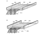
作製基板100上に素子層101を形成する(図1(A)参照。)。素子層101は薄膜トランジスタを含む。次に素子層101を、支持基板102に転置する(図1(B)参照。)。
The
作製基板100は、素子層101の作製工程に合わせて適宜選択すればよい。例えば、作製基板100としては、ガラス基板、石英基板、サファイア基板、セラミック基板、表面に絶縁層が形成された金属基板などを用いることができる。また、処理温度に耐えうる耐熱性を有するプラスチック基板を用いてもよい。
The
支持基板102より、第1の封止部材110に素子層101を転置する(図1(C)参照。)。
The
素子層101と電気的に接続する発光素子125を形成し、素子層101及び発光素子125を覆う第2の封止部材120を形成する。よって、第1の封止部材110と第2の封止部材120とによって封止された素子層101及び発光素子125を含む可撓性の発光パネル155aが作製される(図1(D)参照。)。
A light-emitting
可撓性の発光パネル155aは、一対の封止部材によって封止されていればよく、封止部材は可撓性であれば、基板でも膜でもよい。発光パネル155aは基板状の第1の封止部材110と樹脂層状の第2の封止部材120を用いる例である。封止する手段として、封止部材同士を接着するシール材や、異なる形状の封止部材を複数用いてもよい。図5に可撓性の発光パネルの他の例を示す。
The flexible light-emitting
図5(A)は、樹脂層状の第2の封止部材120上にさらに基板状の第3の封止部材128を設けた可撓性の発光パネル155bの例である。また、図5(B)はさらに、第1の封止部材110と第3の封止部材128をシール材124によって接着した可撓性の発光パネル155cの例である。
FIG. 5A illustrates an example of a flexible light-emitting
第2の封止部材120のような樹脂層状の封止部材は、紫外線硬化樹脂または熱硬化樹脂を用いることができ、PVC(ポリビニルクロライド)、アクリル、ポリイミド、エポキシ樹脂、シリコーン樹脂、PVB(ポリビニルブチラル)またはEVA(エチレンビニルアセテート)を用いることができる。また、封止部材として、乾燥剤などの吸湿性を有する物質を用いる、または封止部材中に吸湿性を有する物質を添加すると、さらなる吸水効果が得られ、素子の劣化を防ぐことができる。
The resin layer-shaped sealing member such as the
シール材124としては、代表的には可視光硬化性、紫外線硬化性または熱硬化性の樹脂を用いるのが好ましい。代表的には、アクリル樹脂、エポキシ樹脂、アミン樹脂などを用いることができる。また、光(代表的には紫外線)重合開始剤、熱硬化剤、フィラー、カップリング剤を含んでもよい。
As the sealing
第1の封止部材110と第3の封止部材128をシール材124によって貼り合わせる工程は減圧下で行ってもよい。
The step of bonding the
支持基板102、第1の封止部材110、及び第3の封止部材128は可撓性を有する基板(可撓性基板)又は膜を用いる。しかし、形状を加工され固定された後の第1の封止部材110、第2の封止部材120、及び第3の封止部材128は可撓性を有する必要はない。支持基板102、第1の封止部材110、第2の封止部材120、及び第3の封止部材128として、アラミド樹脂、ポリエチレンナフタレート(PEN)樹脂、ポリエーテルサルフォン(PES)樹脂、ポリフェニレンサルファイド(PPS)樹脂、ポリイミド(PI)樹脂などを用いることができる。また、繊維に有機樹脂が含浸された構造体であるプリプレグを用いてもよい。透光性を有する必要がない場合、ステンレスなどの金属フィルムを用いてもよい。
As the
封止部材には無機絶縁膜などの保護膜を設けてもよい。例えば、第1の封止部材110において、素子層101側に保護膜を設けると外部や第1の封止部材110から素子層101へ汚染物質が進入するのを保護膜によって遮断できる。また第1の封止部材110において外側(素子層101と反対側)に保護膜を設けると第1の封止部材110自体への汚染物質の進入が遮断でき、劣化を防ぐことができる。
The sealing member may be provided with a protective film such as an inorganic insulating film. For example, when a protective film is provided on the
封止部材には乾燥剤となる吸湿性を有する物質を設けてもよい。例えば、酸化バリウムなどの吸湿性を有する物質の膜を封止基板にスパッタ法により形成すればよい。 The sealing member may be provided with a hygroscopic substance serving as a desiccant. For example, a film of a hygroscopic substance such as barium oxide may be formed over the sealing substrate by a sputtering method.
なお、本明細書において、封止部材や保持部材と、素子層や発光素子との貼り合わせは接着層を用いて行うことができる。転置工程において支持基板への貼り合わせは、後に剥離可能な接着材を用いるとよい。例えば、水溶性の接着材を用いて支持基板と素子層などを一時的に接着し、水によって洗浄することによって支持基板を素子層から剥離すればよい。 Note that in this specification, the sealing member or the holding member can be bonded to the element layer or the light-emitting element by using an adhesive layer. In the transfer step, an adhesive that can be peeled later is preferably used for attachment to the supporting substrate. For example, the support substrate and the element layer may be temporarily bonded using a water-soluble adhesive, and the support substrate may be peeled off from the element layer by washing with water.
可撓性の発光パネル155aの形状を加工して、屈曲させ、曲部を有する発光パネル150を形成する(図1(E)参照。)。形状の加工は、形状の型となる支持体を用いて行ってもよい。
The shape of the flexible light-emitting
発光パネル150を覆うように保護膜126を形成する(図1(F)参照。)。保護膜126を薄膜とすることにより、曲部を有する発光パネル150(図1(E)参照。)の形状を保護膜の形状に反映させることができる。
A
保護膜126を、曲部を有する形状に加工された発光パネル150に対して形成するので、発光パネル150の形状加工による保護膜126の破損などの形状不良を防ぐことができる。よって、緻密な保護膜126によって外部からの水分や他の不純物などを遮断し、発光パネル150を有する発光装置の汚染を防ぐ高い効果が得られる。
Since the
保護膜126は、その材料に応じて、スパッタ法、CVD法、蒸着法、SOG法、スピンコート、ディップ、スプレー塗布、液滴吐出法(インクジェット法、スクリーン印刷、オフセット印刷等)、ドクターナイフ、ロールコーター、カーテンコーター、ナイフコーター等を用いることができる。保護膜126に用いる無機材料としては、酸化珪素、窒化珪素、酸化窒化珪素、酸化アルミニウム、窒化アルミニウム、酸化窒化アルミニウムなどを用いることができる。好ましくは、窒化珪素を用いてスパッタ法により形成するとよい。
The
また、保護膜126として表示部以外の発光素子からの光を取り出さない領域では、部分的に非透光性の金属膜などを用いてもよい。
In addition, in a region where light from a light emitting element other than the display portion is not extracted as the
保護膜126は単層構造でも積層構造でもよい。例えば、発光パネル150を有機樹脂層によって覆い、さらにその上に無機膜によって覆うように積層してもよい。保護膜は大気中に浮遊する有機物や金属物、水蒸気などの汚染不純物の侵入を防ぐ効果のある緻密な膜であれば特に材料及び形成方法には限定されない。
The
保護膜は、必ずしも発光パネルの全表面を覆うように形成されなくてもよく、少なくとも、表示領域として用いる曲折部を含む領域を覆うように形成すればよい。図15(B)は、曲折した発光パネル150の第2の封止部材120側に保護膜130を形成する例である。
The protective film is not necessarily formed so as to cover the entire surface of the light-emitting panel, and may be formed so as to cover at least a region including a bent portion used as a display region. FIG. 15B illustrates an example in which the
また、保護膜は一回の工程で形成してもよいし、複数回成膜してもよい。図15(B)は、曲折した発光パネル150の第2の封止部材120側に保護膜131aを形成し、第1の封止部材110側に保護膜131bを形成する例である。複数回保護膜を形成する場合、保護膜131a、131bのように一部保護膜同士が積層する構造であってもよい。
Further, the protective film may be formed in a single step or may be formed a plurality of times. FIG. 15B illustrates an example in which the
発光パネルにおいて封止部材に覆われない端部を覆うように保護膜を形成すると、発光素子の劣化を防ぐのに効果的である。 When a protective film is formed so as to cover an end portion of the light emitting panel that is not covered with the sealing member, it is effective to prevent deterioration of the light emitting element.
また、本実施の形態では図示しないが、カラーフィルタ(着色層)、ブラックマトリクス(遮光層)、偏光部材、位相差部材、反射防止部材などの光学部材(光学基板)などは適宜設ける。例えば、偏光基板及び位相差基板による円偏光を用いてもよい。 Although not shown in the present embodiment, an optical member (optical substrate) such as a color filter (colored layer), a black matrix (light shielding layer), a polarizing member, a retardation member, or an antireflection member, and the like are provided as appropriate. For example, circularly polarized light using a polarizing substrate and a retardation substrate may be used.
可撓性の発光パネル155aを発光パネル150の形状に変化させる際、その変化させた形状を固定させるために加熱処理や光照射処理などの固定処理を行ってもよい。また、加熱処理によって発光パネル150の形状に変形させ、変形を保持させたまま冷却することによって、発光パネル150の形状を固定させてもよい。
When the flexible light-emitting
素子層101は、直接封止部材110に形成してもよい。例えば、印刷法などを用いて発光素子の電極層を支持基板102や第1の封止部材110に直接形成すればよい。
The
本実施の形態のように作製基板100より素子層101を他の基板へ転置する方法は、特に限定されず種々の方法を用いることができる。例えば作製基板と素子層との間に剥離層を形成すればよい。
A method for transferring the
剥離層は、スパッタリング法やプラズマCVD法、塗布法、印刷法等により、タングステン(W)、モリブデン(Mo)、チタン(Ti)、タンタル(Ta)、ニオブ(Nb)、ニッケル(Ni)、コバルト(Co)、ジルコニウム(Zr)、亜鉛(Zn)、ルテニウム(Ru)、ロジウム(Rh)、パラジウム(Pd)、オスミウム(Os)、イリジウム(Ir)、珪素(Si)から選択された元素、又は元素を主成分とする合金材料、又は前記元素を主成分とする化合物材料からなる層を、単層又は積層して形成する。珪素を含む層の結晶構造は、非晶質、微結晶、多結晶のいずれの場合でもよい。なお、ここでは、塗布法は、スピンコーティング法、液滴吐出法、ディスペンス法を含む。 The release layer is formed by sputtering, plasma CVD, coating, printing, etc., tungsten (W), molybdenum (Mo), titanium (Ti), tantalum (Ta), niobium (Nb), nickel (Ni), cobalt An element selected from (Co), zirconium (Zr), zinc (Zn), ruthenium (Ru), rhodium (Rh), palladium (Pd), osmium (Os), iridium (Ir), silicon (Si), or A layer made of an alloy material containing an element as a main component or a compound material containing the element as a main component is formed as a single layer or a stacked layer. The crystal structure of the layer containing silicon may be any of amorphous, microcrystalline, and polycrystalline. Here, the coating method includes a spin coating method, a droplet discharge method, and a dispensing method.
剥離層が単層構造の場合、好ましくは、タングステン層、モリブデン層、又はタングステンとモリブデンの混合物を含む層を形成する。又は、タングステンの酸化物若しくは酸化窒化物を含む層、モリブデンの酸化物若しくは酸化窒化物を含む層、又はタングステンとモリブデンの混合物の酸化物若しくは酸化窒化物を含む層を形成する。なお、タングステンとモリブデンの混合物とは、例えば、タングステンとモリブデンの合金に相当する。 In the case where the separation layer has a single-layer structure, a tungsten layer, a molybdenum layer, or a layer containing a mixture of tungsten and molybdenum is preferably formed. Alternatively, a layer containing tungsten oxide or oxynitride, a layer containing molybdenum oxide or oxynitride, or a layer containing an oxide or oxynitride of a mixture of tungsten and molybdenum is formed. Note that the mixture of tungsten and molybdenum corresponds to, for example, an alloy of tungsten and molybdenum.
剥離層が積層構造の場合、好ましくは、1層目としてタングステン層、モリブデン層、又はタングステンとモリブデンの混合物を含む層を形成し、2層目として、タングステン、モリブデン又はタングステンとモリブデンの混合物の酸化物、窒化物、酸化窒化物又は窒化酸化物を形成する。 In the case where the separation layer has a stacked structure, preferably, a tungsten layer, a molybdenum layer, or a layer containing a mixture of tungsten and molybdenum is formed as a first layer, and oxidation of tungsten, molybdenum, or a mixture of tungsten and molybdenum is formed as a second layer. An oxide, a nitride, an oxynitride, or a nitrided oxide.
剥離層として、タングステンを含む層とタングステンの酸化物を含む層の積層構造を形成する場合、タングステンを含む層を形成し、その上層に酸化物で形成される絶縁層を形成することで、タングステン層と絶縁層との界面に、タングステンの酸化物を含む層が形成されることを活用してもよい。さらには、タングステンを含む層の表面を、熱酸化処理、酸素プラズマ処理、オゾン水等の酸化力の強い溶液での処理等を行ってタングステンの酸化物を含む層を形成してもよい。またプラズマ処理や加熱処理は、酸素、窒素、一酸化二窒素、あるいは前記ガスとその他のガスとの混合気体雰囲気下で行ってもよい。これは、タングステンの窒化物、酸化窒化物及び窒化酸化物を含む層を形成する場合も同様であり、タングステンを含む層を形成後、その上層に窒化珪素層、酸化窒化珪素層、窒化酸化珪素層を形成するとよい。 In the case of forming a stacked structure of a layer containing tungsten and a layer containing an oxide of tungsten as the separation layer, a tungsten-containing layer is formed, and an insulating layer formed of an oxide is formed thereover. The fact that a layer containing tungsten oxide is formed at the interface between the layer and the insulating layer may be utilized. Further, the layer containing tungsten oxide may be formed by performing thermal oxidation treatment, oxygen plasma treatment, treatment with a strong oxidizing power such as ozone water, or the like on the surface of the layer containing tungsten. Further, the plasma treatment or the heat treatment may be performed in an atmosphere of oxygen, nitrogen, dinitrogen monoxide, or a mixed gas of the above gas and another gas. The same applies to the case where a layer containing tungsten nitride, oxynitride, and nitride oxide is formed. After a layer containing tungsten is formed, a silicon nitride layer, a silicon oxynitride layer, and a silicon nitride oxide layer are formed thereon. A layer may be formed.
なお、他の基板への転置工程は、基板と素子層の間に剥離層を形成し、剥離層と素子層との間に金属酸化膜を設け、当該金属酸化膜を結晶化により脆弱化して、当該素子層を剥離する方法、耐熱性の高い基板と素子層の間に水素を含む非晶質珪素膜を設け、レーザ光の照射またはエッチングにより当該非晶質珪素膜を除去することで、当該素子層を剥離する方法、基板と素子層の間に剥離層を形成し、剥離層と素子層との間に金属酸化膜を設け、当該金属酸化膜を結晶化により脆弱化し、剥離層の一部を溶液やNF3、BrF3、ClF3等のフッ化ハロゲンガスによりエッチングで除去した後、脆弱化された金属酸化膜において剥離する方法、素子層が形成された基板を機械的に削除又は溶液やNF3、BrF3、ClF3等のフッ化ハロゲンガスによるエッチングで除去する方法等を適宜用いることができる。また、剥離層として窒素、酸素や水素等を含む膜(例えば、水素を含む非晶質珪素膜、水素含有合金膜、酸素含有合金膜など)を用い、剥離層にレーザ光を照射して剥離層内に含有する窒素、酸素や水素をガスとして放出させ素子層と基板との剥離を促進する方法を用いてもよい。 In the transfer process to another substrate, a peeling layer is formed between the substrate and the element layer, a metal oxide film is provided between the peeling layer and the element layer, and the metal oxide film is weakened by crystallization. , A method of peeling the element layer, providing an amorphous silicon film containing hydrogen between a highly heat-resistant substrate and the element layer, and removing the amorphous silicon film by laser light irradiation or etching, A method of peeling the element layer, forming a peeling layer between the substrate and the element layer, providing a metal oxide film between the peeling layer and the element layer, weakening the metal oxide film by crystallization, A method in which a part is removed by etching with a fluorinated halogen gas such as NF 3 , BrF 3 , or ClF 3 after etching, and then the substrate on which the element layer is formed is mechanically deleted. Or a solution, a NF 3 , BrF 3 , ClF 3, etc. A method of removing by etching with a halogenated gas can be used as appropriate. In addition, a film containing nitrogen, oxygen, hydrogen, or the like (for example, an amorphous silicon film containing hydrogen, a hydrogen-containing alloy film, an oxygen-containing alloy film, or the like) is used as the separation layer, and the separation layer is irradiated with laser light for separation. A method of releasing nitrogen, oxygen, or hydrogen contained in the layer as a gas and accelerating the separation between the element layer and the substrate may be used.
上記剥離方法を組み合わすことでより容易に転置工程を行うことができる。つまり、レーザ光の照射、ガスや溶液などによる剥離層へのエッチング、鋭いナイフやメスなどによる剥離層の機械的な削除を行い、基板から素子層を剥離しやすい状態にしてから、物理的な力(機械等による)によって剥離を行うこともできる。 A transposition step can be performed more easily by combining the above peeling methods. In other words, laser beam irradiation, etching of the release layer with gas or solution, mechanical removal of the release layer with a sharp knife or scalpel, etc. to make the device layer easy to peel off from the substrate, Peeling can also be performed by force (by machine or the like).
また、剥離層と素子層との界面に液体(例えば水)を浸透させて基板から素子層を剥離してもよい。 Alternatively, the element layer may be peeled from the substrate by infiltrating a liquid (for example, water) into the interface between the peeling layer and the element layer.
発光パネル150の形状は、型となる支持体や保持部材の形状を選択することによって自由に決定することができる。よって、さまざまな場所や用途に対応した形状に、多様に発光装置を作製することができ、利便性の高い発光装置を提供することができる。
The shape of the light-emitting
また、保護膜を設けることによって、素子層や発光素子への不純物の汚染を防止することができ、発光装置の信頼性を向上させることができる。 In addition, by providing the protective film, contamination of impurities to the element layer and the light-emitting element can be prevented, and the reliability of the light-emitting device can be improved.
(実施の形態2)
本実施の形態では、実施の形態1において、発光装置の作製方法の他の例を図2に示す。従って、他は実施の形態1と同様に行うことができ、実施の形態1と同一部分又は同様な機能を有する部分、及び工程の繰り返しの説明は省略する。
(Embodiment 2)
In this embodiment mode, another example of a method for manufacturing a light-emitting device in
図2は発光装置及び発光装置の作製方法を示す断面図である。 FIG. 2 is a cross-sectional view illustrating a light-emitting device and a method for manufacturing the light-emitting device.
本実施の形態では、電極層や素子層を作製後、形状を成形する加工を行うことによって少なくとも一部が曲折した発光パネルを作製し、少なくとも一部が曲折した発光パネル表面を覆う保護膜を形成して、当該発光パネルを用いた発光装置に高機能化及び高信頼性を付加する。 In this embodiment mode, after forming an electrode layer or an element layer, a light emitting panel that is bent at least partially is manufactured by performing a process of forming a shape, and a protective film that covers the surface of the light emitting panel that is bent at least partially is formed. Thus, high functionality and high reliability are added to a light emitting device using the light emitting panel.
作製基板100上に素子層101及び素子層101と電気的に接続する発光素子125を形成し、素子層101及び発光素子125を覆う第2の封止部材120を形成する(図2(A)参照。)。素子層101は薄膜トランジスタを含む。次に素子層101、発光素子125及び第2の封止部材120を、第3の封止部材128に転置する(図2(B)参照。)。
The
発光装置の形状の型となる支持体111を用い、素子層101、発光素子125、第2の封止部材120、及び第3の封止部材128を、第3の封止部材128が支持体111に接するように、支持体111の曲折部の曲面にそって設ける(図2(C)参照。)。第3の封止部材128は支持体111に固着されればよく、接着層などで貼り付ければよい。
The
露出している素子層101側に第1の封止部材110を貼り合わせ、曲折した発光パネル151を形成する(図2(D)参照。)。
The
素子層101、発光素子125、第2の封止部材120、及び第3の封止部材128、及び第1の封止部材110の形状を変化させる際、その変化させた形状を固定させるために加熱処理や光照射処理などの固定処理を行ってもよい。また、加熱処理によって素子層101、発光素子125、第2の封止部材120、第3の封止部材128、及び第1の封止部材110の形状を変形させ、変形を保持させたまま冷却することによって、該形状を固定させてもよい。
In order to fix the changed shapes when the shapes of the
成形処理によって曲折した発光パネル151を形成した後、曲折した発光パネル151より支持体111を除去する。
After forming the bent
実施の形態1同様に、曲折した発光パネル151を覆うように保護膜126を形成する(図2(E)参照。)。以上の工程で曲折した発光パネル151を含む発光装置を作製することができる。
As in
図2においては、第3の封止部材128に素子層101、発光素子125及び第2の封止部材120を接着した後、第3の封止部材128に素子層101、発光素子125及び第2の封止部材120を支持体111によって曲折するように成形工程を行う例を示したが、曲折するように成形された封止部材に、素子層101、発光素子125、及び第2の封止部材120を接着する例を図13に示す。
In FIG. 2, after the
作製基板100上に素子層101及び素子層101と電気的に接続する発光素子125を形成し、素子層101及び発光素子125を覆う第2の封止部材120を形成する(図13(A)参照。)。次に素子層101、発光素子125及び第2の封止部材120を、支持基板102に転置する(図13(B)参照。)。
The
発光装置の形状の型となる支持体111を用い、第1の封止部材110を、支持体111の曲折部の曲面にそって設ける。第1の封止部材110は支持体111に固着されればよく、接着層などで貼り付ければよい。
The
素子層101と第1の封止部材110とが対向するように、支持基板102と支持体111とを配置し、素子層101が第1の封止部材110と接するように、素子層101、発光素子125、及び第2の封止部材120を矢印の方向に第1の封止部材110側に転置する(図13(C)参照。)。
The
露出している第2の封止部材120側に第3の封止部材128を貼り合わせ、曲折した発光パネル152を形成する(図13(D)参照。)。
A
曲折した発光パネル152を覆うように保護膜126を形成する(図13(E)参照。)。以上の工程で曲折した発光パネル152を含む発光装置を作製することができる。
A
形状を加工するための成形工程を行う順序によって、発光パネル151と発光パネル152のように曲折する方向が異なる発光パネルを作製することができる。また支持体111の形状を選択することで、支持体111の形状を反映した発光パネルを作製することができる。
A light-emitting panel having different bending directions, such as the light-emitting
発光パネルの形状は、型となる支持体や保持部材の形状を選択することによって自由に決定することができる。よって、さまざまな場所や用途に対応した形状に、多様に発光装置を作製することができ、利便性の高い発光装置を提供することができる。 The shape of the light-emitting panel can be freely determined by selecting the shape of the support or holding member serving as a mold. Therefore, a variety of light-emitting devices can be manufactured in shapes corresponding to various places and uses, and a highly convenient light-emitting device can be provided.
また、保護膜を設けることによって、素子層や発光素子への不純物の汚染を防止することができ、発光装置の信頼性を向上させることができる。 In addition, by providing the protective film, contamination of impurities to the element layer and the light-emitting element can be prevented, and the reliability of the light-emitting device can be improved.
(実施の形態3)
本実施の形態では、実施の形態1又は実施の形態2において、保持部材を用いる発光装置の例を図3及び図4に示す。従って、他は実施の形態1又は実施の形態2と同様に行うことができ、実施の形態1又は実施の形態2と同一部分又は同様な機能を有する部分、及び工程の繰り返しの説明は省略する。
(Embodiment 3)
In this embodiment mode, an example of a light-emitting device using a holding member in
図3及び図4は本実施の形態の発光装置を示す図である。 3 and 4 are diagrams showing the light-emitting device of this embodiment.
本実施の形態では、発光装置の作製工程において、電極層や素子層の作製後、発光パネルの形状を成形する加工を行い、当該発光パネルを用いた発光装置に高機能化を付加する。また、さらに保護膜を設け、発光装置の信頼性を向上させる。なお、本実施の形態では、少なくとも一部が曲折する形状に成形された発光装置の該形状を保持するために、保持部材を用いる。 In this embodiment mode, in the manufacturing process of the light-emitting device, after forming the electrode layer and the element layer, a process for forming the shape of the light-emitting panel is performed, and high functionality is added to the light-emitting device using the light-emitting panel. Further, a protective film is provided to improve the reliability of the light emitting device. Note that in this embodiment mode, a holding member is used to hold the shape of the light-emitting device that is formed into a shape in which at least a part is bent.
図3(A)乃至(C)は第1の封止部材110と第2の封止部材120との間に素子層101、発光素子125を封止し、保護膜126によって覆われた曲折した発光パネル150を、保持部材に貼り付けて、発光パネル150の形状が固定(保持)された発光装置の例である。なお、発光パネル150において光は第1の封止部材110を透過して視認側に放射される。
3A to 3C, the
図3(A)は、発光パネル150において曲折部の外側(第1の封止部材110側)の保護膜126と接するように保持部材129aを設けている。図3(B)は、発光パネル150において曲折部の内側(第2の封止部材120側)の保護膜126と接するように保持部材129bを設けている。図3(C)は、発光パネル150において曲折部の内側(第2の封止部材120側)を充填するように保護膜126と接して保持部材129cを設けている。
3A, the holding
保持部材129a、129b、129cと保護膜126とは接着層を用いて固定してもよい。また、保持部材129cのように発光パネルの曲折部内側を充填するように設けられる場合、保持部材129cをシール材などに用いられる光硬化性樹脂や、熱硬化性樹脂などを用いて、発光パネル150に接着して設け、発光パネル150の形状を保持してもよい。
The holding
保持部材129a、129b、129cは、発光パネル150の光を取り出す表示側に設ける場合は、透光性の材料を用いる。よって、発光パネル150において光は第1の封止部材110を透過して視認側に放射される場合、図3(A)で用いる保持部材129aは透光性の保持部材を用い、図3(B)(C)の保持部材129b、129cは透光性である必要はなく、反射性の材料を用いると発光パネル150からの光の取り出し効率が向上する効果がある。発光パネル150が第1の封止部材110及び第2の封止部材120両方から光を取り出す構造であれば、保持部材129a、129b、129cは透光性である必要がある。
When the holding
図3(A)乃至(C)においては、保護膜126で覆われた発光パネル150に保持部材を設ける例を示したが、図4(A)乃至(C)に示すように、発光パネルに保持部材を設けた後、発光パネル及び保持部材の表面を覆うように保護膜を形成してもよい。
FIGS. 3A to 3C show an example in which a holding member is provided on the light-emitting
発光パネル150の形状は、型となる支持体や保持部材の形状を選択することによって自由に決定することができる。よって、さまざまな場所や用途に対応した形状に、多様に発光装置を作製することができ、利便性の高い発光装置を提供することができる。
The shape of the light-emitting
また、保護膜を設けることによって、素子層や発光素子への不純物の汚染を防止することができ、発光装置の信頼性を向上させることができる。 In addition, by providing the protective film, contamination of impurities to the element layer and the light-emitting element can be prevented, and the reliability of the light-emitting device can be improved.
(実施の形態4)
本実施の形態では、実施の形態1乃至3において、大型の基板に複数の発光装置の素子層を作製する例(所謂多面取り)、を図7に示す。従って、他は実施の形態1乃至3と同様に行うことができ、実施の形態1乃至3と同一部分又は同様な機能を有する部分、及び工程の繰り返しの説明は省略する。
(Embodiment 4)
In this embodiment mode, an example of manufacturing a plurality of light-emitting device element layers over a large substrate in
上記実施の形態において、作製基板100上に素子層101を形成し、作製基板100から可撓性基板である支持基板102へ素子層101を転置する。
In the above embodiment, the
大型の作製基板より、複数の素子層を支持基板へ転置し、当該支持基板を複数の支持基板に分断する方法を図7に示す。図7(A2)(B2)(C2)は平面図であり、図7(A1)(B1)(C1)は、図7(A2)(B2)(C2)それぞれにおける線X−Yの断面図である。 FIG. 7 shows a method for transferring a plurality of element layers to a supporting substrate from a large manufacturing substrate and dividing the supporting substrate into a plurality of supporting substrates. FIGS. 7A2, B2, and C2 are plan views, and FIGS. 7A1, B1, and C1 are cross-sectional views taken along line XY in FIGS. 7A2, B2, and C2, respectively. It is.
大型の作製基板180に、素子層101a、101b、101cを形成する(図7(A1)(A2)参照。)。
作製基板180と同等な大きさの支持基板182を素子層101a、101b、101cと対向して配置し、作製基板180より矢印の方向へ素子層101a、101b、101cを支持基板182へ転置する(図7(B1)(B2)参照。)。
A supporting
支持基板182を各素子層101a、素子層101b、素子層101cごとに支持基板102a、支持基板102b、支持基板102cに分断する(図7(C1)(C2)参照。)。分断手段としては物理的に分断することができれば特に限定はなく、ダイサー、スクライバー等を用いてもよいし、レーザ光を照射することによって分断してもよい。
The
各パネル毎に支持基板102(102a、102b、102c)上に形成された素子層101(101a、101b、101c)をそれぞれ用いて発光装置を作製する。後の工程は、実施の形態1乃至3と同様に行えばよい。
A light emitting device is manufactured using the element layer 101 (101a, 101b, 101c) formed on the supporting substrate 102 (102a, 102b, 102c) for each panel. The subsequent steps may be performed in the same manner as in
このように、大型基板を用いて一度に複数の発光装置に用いることのできる素子層の転置工程を行うと、生産性を向上させることができる。 Thus, productivity can be improved by performing a transfer process of an element layer that can be used for a plurality of light-emitting devices at a time using a large substrate.
(実施の形態5)
本明細書に開示する発明は、パッシブマトリクス型の発光装置でもアクティブマトリクス型の発光装置にも適用することができる。
(Embodiment 5)
The invention disclosed in this specification can be applied to either a passive matrix light-emitting device or an active matrix light-emitting device.
薄膜トランジスタを作製し、該薄膜トランジスタを画素部、さらには駆動回路に用いて表示機能を有する発光装置を作製することができる。また、薄膜トランジスタを用いた駆動回路の一部または全体を、画素部と同じ基板上に一体形成し、システムオンパネルを形成することができる。 A thin film transistor is manufactured, and a light emitting device having a display function can be manufactured using the thin film transistor in a pixel portion and further in a driver circuit. In addition, part or the whole of a driver circuit using a thin film transistor can be formed over the same substrate as the pixel portion to form a system-on-panel.
発光装置は表示素子として発光素子(EL素子ともいう)を含む。 The light-emitting device includes a light-emitting element (also referred to as an EL element) as a display element.
また、発光装置は、表示素子が封止された状態にあるパネルと、該パネルにコントローラを含むIC等を実装した状態にあるモジュールとを含む。本実施の形態では、発光装置のモジュールを図6、図8及び図14に示す。 In addition, the light-emitting device includes a panel in which the display element is sealed, and a module in which an IC or the like including a controller is mounted on the panel. In this embodiment mode, modules of the light-emitting device are shown in FIGS.
なお、本明細書中における発光装置とは、画像表示デバイス、表示デバイス、もしくは光源(照明装置含む)を指す。また、コネクター、例えばFPC(Flexible printed circuit)もしくはTAB(Tape Automated Bonding)テープもしくはTCP(Tape Carrier Package)が取り付けられたモジュール、TABテープやTCPの先にプリント配線板が設けられたモジュール、または表示素子にCOG(Chip On Glass)方式によりIC(集積回路)が直接実装されたモジュールも全て発光装置に含むものとする。 Note that a light-emitting device in this specification refers to an image display device, a display device, or a light source (including a lighting device). Also, a connector, for example, a module with a FPC (Flexible printed circuit) or TAB (Tape Automated Bonding) tape or TCP (Tape Carrier Package), a module with a printed wiring board at the end of a TAB tape or TCP, or a display All modules in which an IC (integrated circuit) is directly mounted on the element by a COG (Chip On Glass) method are also included in the light emitting device.
発光装置の一形態に相当する発光パネル(発光表示パネルともいう)の外観及び断面について、図6、図8及び図14を用いて説明する。図6、図8及び図14は、発光パネル4000にFPC4018が取り付けられた発光モジュール(発光表示モジュールともいう)の例であり、第1の封止部材4001上に形成された薄膜トランジスタ4010、4011、及び発光素子4513を、第1の封止部材4001と第3の封止部材4006との間にシール材4005によって封止している。図6(A)(B)は発光モジュールの斜視図、図8は、図6(A)のM−Nにおける断面図に相当する。第1の封止部材4001及び第3の封止部材4006は素子層及び発光素子を挟持して封止する封止部材である。発光パネル4000は該表面を保護膜4007で覆われており、保護膜4007はFPC4018との接続領域においては開口を有している。
The appearance and a cross section of a light-emitting panel (also referred to as a light-emitting display panel), which is one embodiment of the light-emitting device, will be described with reference to FIGS. 6, 8, and 14 are examples of a light-emitting module (also referred to as a light-emitting display module) in which an
また、図6(B)の発光モジュールは、透光性の保持部材4040に発光パネル4000を固定する例である。発光パネル4000は透光性の保持部材4040に内接して設けられている。
6B is an example in which the light-emitting
図6(A)(B)に示すように、表示領域として機能する画素部4002は、側面と底面を有するように曲折する発光パネルの側面及び底面に連続的に設けられており、底面に第1の表示領域、側面に第2の表示領域を設けることができる。
6A and 6B, the
図14(A)乃至(C)は発光モジュールの他の例であり、発光パネル4000にFPC4018を実装した後、保護膜4007を設ける構成である。図14(A)乃至(C)において、素子層及び発光素子は素子部4050で表している。図14(A)は第1の封止部材4001、素子部4050、第3の封止部材4006に電気的に接続するFPC4018を発光パネル4000に異方性導電膜4019によって実装した後、発光パネル4000及びFPC4018ごと保護膜4007で覆う構成である。
14A to 14C illustrate another example of a light-emitting module, in which a
図14(B)は、第1の封止部材4001と第3の封止部材4006とが積層しない領域に接着層4051を充填するように形成し、接着層4051に封止部材4052を接着して設けている。封止部材4052を設けることで発光パネル4000の物理的強度を向上させることができる。図14(B)は、発光パネル4000、封止部材4052、及びFPC4018ごと保護膜4007で覆う構成である。
In FIG. 14B, an
図14(C)は、図14(B)と同様に第1の封止部材4001と第3の封止部材4006とが積層しない領域に接着層4051を充填するように形成し、接着層4051に封止部材4052を接着して設けている。さらに、発光パネル4000、封止部材4052、及びFPC4018を覆う樹脂層4053を形成し、その表面を平坦化する。図14(C)は、樹脂層4053によって平坦化された表面に保護膜4007を覆うように形成する構成である。
14C is formed so that the
第1の封止部材4001上に設けられた画素部4002と、走査線駆動回路4004とを囲むようにして、シール材4005が設けられている。また画素部4002と、走査線駆動回路4004の上に第3の封止部材4006が設けられている。よって画素部4002と、走査線駆動回路4004とは、第1の封止部材4001とシール材4005と第3の封止部材4006とによって、発光素子4513と共に封止されている。
A
また、シール材によって囲まれている領域とは異なる領域に、別途用意された基板上に単結晶半導体膜又は多結晶半導体膜で形成された信号線駆動回路4003がTAB方法によって実装されている。
In addition, a signal
また別途形成された信号線駆動回路4003と、走査線駆動回路4004または画素部4002に与えられる各種信号及び電位は、FPC4018から供給されている。
In addition, a variety of signals and potentials are supplied to the signal
図8では、接続端子電極4015が、第1の電極層4030と同じ導電膜から形成され、端子電極4016は、薄膜トランジスタ4010、4011のソース電極層及びドレイン電極層と同じ導電膜で形成されている。
In FIG. 8, the
接続端子電極4015は、FPC4018が有する端子と、異方性導電膜4019を介して電気的に接続されている。
The
なお、別途形成した駆動回路の接続方法は、特に限定されるものではなく、COG方法、ワイヤボンディング方法、或いはTAB方法などを用いることができる。 Note that a connection method of a driver circuit which is separately formed is not particularly limited, and a COG method, a wire bonding method, a TAB method, or the like can be used.
また第1の封止部材4001上に設けられた画素部4002と、走査線駆動回路4004は、薄膜トランジスタを複数有しており、図8では、画素部4002に含まれる薄膜トランジスタ4010と、走査線駆動回路4004に含まれる薄膜トランジスタ4011とを例示している。薄膜トランジスタ4010、4011上には絶縁層4020、4021が設けられている。なお、絶縁膜4023は下地膜として機能する絶縁膜である。
Further, the
薄膜トランジスタ4010、4011は、特に限定されず様々な薄膜トランジスタを適用することができる。図8では、薄膜トランジスタ4010、4011として、ボトムゲート構造の逆スタガ薄膜トランジスタを用いる例を示す。薄膜トランジスタ4010、4011はチャネルエッチ型を示すが、半導体層上にチャネル保護膜を設けたチャネル保護型の逆スタガ薄膜トランジスタを用いてもよい。
The
エレクトロルミネッセンスを利用する発光素子は、発光材料が有機化合物であるか、無機化合物であるかによって区別され、一般的に、前者は有機EL素子、後者は無機EL素子と呼ばれている。 A light-emitting element using electroluminescence is distinguished depending on whether the light-emitting material is an organic compound or an inorganic compound. Generally, the former is called an organic EL element and the latter is called an inorganic EL element.
有機EL素子は、発光素子に電圧を印加することにより、一対の電極から電子および正孔がそれぞれ発光性の有機化合物を含む層に注入され、電流が流れる。そして、それらキャリア(電子および正孔)が再結合することにより、発光性の有機化合物が励起状態を形成し、その励起状態が基底状態に戻る際に発光する。このようなメカニズムから、このような発光素子は、電流励起型の発光素子と呼ばれる。 In the organic EL element, by applying a voltage to the light emitting element, electrons and holes are respectively injected from the pair of electrodes into the layer containing the light emitting organic compound, and a current flows. Then, these carriers (electrons and holes) recombine, whereby the light-emitting organic compound forms an excited state, and emits light when the excited state returns to the ground state. Due to such a mechanism, such a light-emitting element is referred to as a current-excitation light-emitting element.
無機EL素子は、その素子構成により、分散型無機EL素子と薄膜型無機EL素子とに分類される。分散型無機EL素子は、発光材料の粒子をバインダ中に分散させた発光層を有するものであり、発光メカニズムはドナー準位とアクセプター準位を利用するドナー−アクセプター再結合型発光である。薄膜型無機EL素子は、発光層を誘電体層で挟み込み、さらにそれを電極で挟んだ構造であり、発光メカニズムは金属イオンの内殻電子遷移を利用する局在型発光である。なお、ここでは、発光素子として有機EL素子を用いて説明する。 Inorganic EL elements are classified into a dispersion-type inorganic EL element and a thin-film inorganic EL element depending on the element structure. The dispersion-type inorganic EL element has a light-emitting layer in which particles of a light-emitting material are dispersed in a binder, and the light emission mechanism is donor-acceptor recombination light emission using a donor level and an acceptor level. The thin-film inorganic EL element has a structure in which a light emitting layer is sandwiched between dielectric layers and further sandwiched between electrodes, and the light emission mechanism is localized light emission utilizing inner-shell electron transition of metal ions. Note that description is made here using an organic EL element as a light-emitting element.
発光素子は発光を取り出すために少なくとも一対の電極の一方が透明であればよい。そして、基板上に薄膜トランジスタ及び発光素子を形成し、基板とは逆側の面から発光を取り出す上面射出や、基板側の面から発光を取り出す下面射出や、基板側及び基板とは反対側の面から発光を取り出す両面射出構造の発光素子があり、どの射出構造の発光素子も適用することができる。 In order to extract light emitted from the light-emitting element, at least one of the pair of electrodes may be transparent. Then, a thin film transistor and a light emitting element are formed on the substrate, and a top emission that extracts light from a surface opposite to the substrate, a bottom emission that extracts light from a surface on the substrate, and a surface opposite to the substrate and the substrate are provided. There is a light-emitting element having a dual emission structure in which light emission is extracted from the light-emitting element, and any light-emitting element having an emission structure can be applied.
図8に示す発光素子4513は、画素部4002に設けられた薄膜トランジスタ4010と電気的に接続している。なお発光素子4513の構成は、第1の電極層4030、電界発光層(EL層)4511、第2の電極層4031の積層構造であるが、示した構成に限定されない。発光素子4513から取り出す光の方向などに合わせて、発光素子4513の構成は適宜変えることができる。
A light-emitting
隔壁4510は、有機樹脂膜、無機絶縁膜または有機ポリシロキサン膜を用いて形成する。特に感光性の材料を用い、第1の電極層4030上に開口部を形成し、その開口部の側壁が連続した曲率を持って形成される傾斜面となるように形成することが好ましい。
A
電界発光層4511は、単数の層で構成されていても、複数の層が積層されるように構成されていてもどちらでも良い。
The
発光素子4513に酸素、水素、水分、二酸化炭素等が侵入しないように、第2の電極層4031及び隔壁4510上に保護膜を形成してもよい。保護膜としては、窒化珪素膜、窒化酸化珪素膜、DLC膜等を形成することができる。また、第1の封止部材4001、第3の封止部材4006、及びシール材4005によって封止された空間には充填材として機能する第2の封止部材4514が設けられ密封されている。このように外気に曝されないように気密性が高く、脱ガスの少ない保護フィルム(貼り合わせフィルム、紫外線硬化樹脂フィルム等)やカバー材でパッケージング(封入)することが好ましい。
A protective film may be formed over the
第2の封止部材4514として、紫外線硬化樹脂または熱硬化樹脂を用いることができ、PVC(ポリビニルクロライド)、アクリル、ポリイミド、エポキシ樹脂、シリコーン樹脂、PVB(ポリビニルブチラル)またはEVA(エチレンビニルアセテート)を用いることができる。第2の封止部材4514の代わりに充填材としては窒素やアルゴンなどの不活性な気体を設けてもよい。例えば充填材として窒素を用いればよい。
An ultraviolet curable resin or a thermosetting resin can be used as the
また、必要であれば、発光素子の射出面に偏光板、又は円偏光板(楕円偏光板を含む)、位相差板(λ/4板、λ/2板)、カラーフィルタなどの光学フィルムを適宜設けてもよい。また、偏光板又は円偏光板に反射防止膜を設けてもよい。例えば、表面の凹凸により反射光を拡散し、映り込みを低減できるアンチグレア処理を施すことができる。 If necessary, an optical film such as a polarizing plate, a circular polarizing plate (including an elliptical polarizing plate), a retardation plate (λ / 4 plate, λ / 2 plate), a color filter, or the like is provided on the light emitting element exit surface. You may provide suitably. Further, an antireflection film may be provided on the polarizing plate or the circularly polarizing plate. For example, anti-glare treatment can be performed that diffuses reflected light due to surface irregularities and reduces reflection.
単色の発光を示す材料を形成し、カラーフィルタや色変換層を組み合わせることによりフルカラー表示を行うことができる。もちろん単色発光の表示を行ってもよい。 Full color display can be performed by forming a material exhibiting monochromatic light emission and combining a color filter and a color conversion layer. Of course, monochromatic light emission may be displayed.
カラーフィルタとして機能する着色層や、色変換層は、発光素子を封止部材間に封止して発光パネルを形成した後、各画素に対応して発光パネルに貼り合わせて設けてもよいし、発光素子と共に封止部材間に封止して設けてもよい。着色層を封止部材間に設ける場合、着色層、素子層、及び発光素子の積層順は特に限定されず、第1の封止部材、着色層、素子層、発光素子、第2の封止部材の積層でもよいし、第1の封止部材、素子層、着色層、発光素子、第2の封止部材の積層、第1の封止部材、素子層、発光素子、着色層、第2の封止部材の積層でもよい。着色層は発光素子からの光が外部へ放射される前に、該光が通過する位置に設ければよい。 A colored layer or a color conversion layer that functions as a color filter may be provided by sealing a light emitting element between sealing members to form a light emitting panel and then bonding the light emitting panel to the light emitting panel corresponding to each pixel. The light emitting element and the sealing member may be sealed between the sealing members. When the colored layer is provided between the sealing members, the order in which the colored layer, the element layer, and the light emitting element are stacked is not particularly limited, and the first sealing member, the colored layer, the element layer, the light emitting element, and the second sealing member. The first sealing member, the element layer, the colored layer, the light emitting element, the second sealing member may be stacked, the first sealing member, the element layer, the light emitting element, the colored layer, the second layer. The sealing member may be laminated. The colored layer may be provided at a position where the light passes before the light from the light emitting element is emitted to the outside.
電界発光層4511に含まれる発光層は、発光波長帯の異なる発光層を画素毎に形成して、カラー表示を行う構成としても良い。典型的には、R(赤)、G(緑)、B(青)の各色に対応した発光層を形成する。また白色発光を組み合わせてもよい。この場合にも、画素の光放射側にその発光波長帯の光を透過するフィルターを設けた構成とすることで、色純度の向上や、画素領域の鏡面化(映り込み)の防止を図ることができる。
The light-emitting layer included in the
なお、第1の封止部材4001、第3の封止部材4006としては、プラスチックなどを用いることができる。プラスチックとしては、FRP(Fiberglass−Reinforced Plastics)板、PVF(ポリビニルフルオライド)フィルム、ポリエステルフィルムまたはアクリル樹脂フィルムを用いることができる。また、アルミニウムホイルをPVFフィルムやポリエステルフィルムで挟んだ構造のシートを用いることもできる。また透光性を有する必要がない場合、ステンレスなどの金属フィルムを用いてもよい。
Note that plastic or the like can be used for the
絶縁層4020は薄膜トランジスタの保護膜として機能する。
The insulating
なお、保護膜は、大気中に浮遊する有機物や金属物、水蒸気などの汚染不純物の侵入を防ぐためのものであり、緻密な膜が好ましい。保護膜は、スパッタ法を用いて、酸化珪素膜、窒化珪素膜、酸化窒化珪素膜、窒化酸化珪素膜、酸化アルミニウム膜、窒化アルミニウム膜、酸化窒化アルミニウム膜、又は窒化酸化アルミニウム膜の単層、又は積層で形成すればよい。 Note that the protective film is for preventing entry of contaminant impurities such as organic substances, metal substances, and water vapor floating in the atmosphere, and a dense film is preferable. The protective film is formed by sputtering, using a silicon oxide film, a silicon nitride film, a silicon oxynitride film, a silicon nitride oxide film, an aluminum oxide film, an aluminum nitride film, an aluminum oxynitride film, or an aluminum nitride oxide film, Alternatively, a stacked layer may be formed.
また、平坦化絶縁膜として機能する絶縁層4021は、ポリイミド、アクリル樹脂、ベンゾシクロブテン系樹脂、ポリアミド、エポキシ樹脂等の、耐熱性を有する有機材料を用いることができる。また上記有機材料の他に、低誘電率材料(low−k材料)、シロキサン系樹脂、PSG(リンガラス)、BPSG(リンボロンガラス)等を用いることができる。なお、これらの材料で形成される絶縁膜を複数積層させることで、絶縁層4021を形成してもよい。
The insulating
絶縁層4020、絶縁層4021の形成法は、特に限定されず、その材料に応じて、スパッタ法、CVD法、蒸着法、SOG法、スピンコート、ディップ、スプレー塗布、液滴吐出法(インクジェット法、スクリーン印刷、オフセット印刷等)等を用いることができる。また、絶縁層4020、絶縁層4021の形成には、ドクターナイフ、ロールコーター、カーテンコーター、ナイフコーター等を用いることができる。絶縁層を材料液を用いて形成する場合、ベークする工程で同時に、半導体層のアニール(200℃〜400℃)を行ってもよい。絶縁層の焼成工程と半導体層のアニールを兼ねることで効率よく発光装置を作製することが可能となる。
The formation method of the insulating
発光パネルは発光素子からの光を透過させて表示を行う。よって光が透過する表示部(発光部)に設けられる封止部材の他、絶縁膜、導電膜などの薄膜はすべて可視光の波長領域の光に対して透光性とする。 The light-emitting panel performs display by transmitting light from the light-emitting element. Therefore, thin films such as an insulating film and a conductive film in addition to a sealing member provided in a display portion (light-emitting portion) through which light is transmitted have a light-transmitting property with respect to light in the visible wavelength region.
発光素子に電圧を印加する第1の電極層及び第2の電極層(画素電極層、対向電極層などともいう)においては、取り出す光の方向、電極層が設けられる場所、及び電極層のパターン構造によって透光性、反射性を選択すればよい。 In the first electrode layer and the second electrode layer (also referred to as a pixel electrode layer, a counter electrode layer, or the like) for applying a voltage to the light-emitting element, the direction of light to be extracted, the place where the electrode layer is provided, and the pattern of the electrode layer What is necessary is just to select translucency and reflectivity by a structure.
第1の電極層4030、第2の電極層4031は、酸化タングステンを含むインジウム酸化物、酸化タングステンを含むインジウム亜鉛酸化物、酸化チタンを含むインジウム酸化物、酸化チタンを含むインジウム錫酸化物、インジウム錫酸化物(以下、ITOと示す。)、インジウム亜鉛酸化物、酸化ケイ素を添加したインジウム錫酸化物などの透光性を有する導電性材料を用いることができる。
The
また、第1の電極層4030、第2の電極層4031はタングステン(W)、モリブデン(Mo)、ジルコニウム(Zr)、ハフニウム(Hf)、バナジウム(V)、ニオブ(Nb)、タンタル(Ta)、クロム(Cr)、コバルト(Co)、ニッケル(Ni)、チタン(Ti)、白金(Pt)、アルミニウム(Al)、銅(Cu)、銀(Ag)等の金属、又はその合金、若しくはその金属窒化物から一つ、又は複数種を用いて形成することができる。
The
また、第1の電極層4030、第2の電極層4031として、導電性高分子(導電性ポリマーともいう)を含む導電性組成物を用いて形成することができる。導電性高分子としては、いわゆるπ電子共役系導電性高分子が用いることができる。例えば、ポリアニリンまたはその誘導体、ポリピロールまたはその誘導体、ポリチオフェンまたはその誘導体、若しくはこれらの2種以上の共重合体などがあげられる。
Alternatively, the
また、薄膜トランジスタは静電気などにより破壊されやすいため、ゲート線またはソース線に対して、駆動回路保護用の保護回路を同一基板(封止部材)上に設けることが好ましい。保護回路は、非線形素子を用いて構成することが好ましい。 Further, since the thin film transistor is easily broken by static electricity or the like, it is preferable to provide a protective circuit for driving circuit protection on the same substrate (sealing member) for the gate line or the source line. The protection circuit is preferably configured using a non-linear element.
また図8においては、信号線駆動回路を別途形成し、第1の封止部材4001に実装する例を示しているが、この構成に限定されない。走査線駆動回路を別途形成して実装しても良いし、信号線駆動回路の一部または走査線駆動回路の一部のみを別途形成して実装しても良い。
FIG. 8 illustrates an example in which a signal line driver circuit is separately formed and mounted on the
本実施の形態は、他の実施の形態に記載した構成と適宜組み合わせて実施することが可能である。 This embodiment can be implemented in appropriate combination with the structures described in the other embodiments.
(実施の形態6)
本明細書で開示する発光装置が有する薄膜トランジスタは特に限定されない。よって薄膜トランジスタの構造や用いる半導体材料は種々の用いることができる。
(Embodiment 6)
There is no particular limitation on the thin film transistor included in the light-emitting device disclosed in this specification. Therefore, various structures and semiconductor materials can be used for the thin film transistor.
薄膜トランジスタの構造の例を、図9を用いて説明する。図9は、実施の形態5における薄膜トランジスタ4010に用いることのできる薄膜トランジスタの例であり、図9は図8と対応している。
An example of the structure of the thin film transistor will be described with reference to FIGS. FIG. 9 illustrates an example of a thin film transistor that can be used for the
図9(A)乃至(D)において、第1の封止部材4001上に絶縁膜4023が形成され、絶縁膜4023上に薄膜トランジスタ4010a、4010b、4010c、4010dが設けられている。薄膜トランジスタ4010a、4010b、4010c、4010d上に絶縁層4020、絶縁層4021が形成され、薄膜トランジスタ4010a、4010b、4010c、4010dと電気的に接続する第1の電極層4030が設けられている。
9A to 9D, an insulating
薄膜トランジスタ4010aは、図8における薄膜トランジスタ4010において、ソース電極層及びドレイン電極層として機能する配線層405a、405bと半導体層403とがn+層を介さずに接する構成である。
A
薄膜トランジスタ4010aは逆スタガ型の薄膜トランジスタであり、絶縁表面を有する基板である第1の封止部材4001、絶縁膜4023上に、ゲート電極層401、ゲート絶縁層402、半導体層403、ソース電極層又はドレイン電極層として機能する配線層405a、405bを含む。
The
薄膜トランジスタ4010bはボトムゲート型の薄膜トランジスタであり、絶縁表面を有する基板である第1の封止部材4001、絶縁膜4023上に、ゲート電極層401、ゲート絶縁層402、ソース電極層又はドレイン電極層として機能する配線層405a、405b、ソース領域又はドレイン領域として機能するn+層404a、404b、及び半導体層403を含む。また、薄膜トランジスタ4010bを覆い、半導体層403に接する絶縁層4020が設けられている。
The
なお、n+層404a、404bを、ゲート絶縁層402と配線層405a、405bの間に設ける構造としてもよい。また、n+層をゲート絶縁層及び配線層の間と、配線層と半導体層の間と両方に設ける構造としてもよい。n+層404a、404bは、半導体層403より低抵抗な半導体層である。
Note that the n + layers 404a and 404b may be provided between the
薄膜トランジスタ4010bは、薄膜トランジスタ4010bを含む領域全てにおいてゲート絶縁層402が存在し、ゲート絶縁層402と絶縁表面を有する基板である第1の封止部材4001の間にゲート電極層401が設けられている。ゲート絶縁層402上には配線層405a、405b、及びn+層404a、404bが設けられている。そして、ゲート絶縁層402、配線層405a、405b、及びn+層404a、404b上に半導体層403が設けられている。また、図示しないが、ゲート絶縁層402上には配線層405a、405bに加えて配線層を有し、該配線層は半導体層403の外周部より外側に延在している。
In the
薄膜トランジスタ4010cは、薄膜トランジスタ4010bにおいて、ソース電極層及びドレイン電極層と半導体層とが、n+層を介さずに接する構成である。
The
薄膜トランジスタ4010cは、薄膜トランジスタ4010cを含む領域全てにおいてゲート絶縁層402が存在し、ゲート絶縁層402と絶縁表面を有する基板である第1の封止部材4001の間にゲート電極層401が設けられている。ゲート絶縁層402上には配線層405a、405bが設けられている。そして、ゲート絶縁層402、配線層405a、405b上に半導体層403が設けられている。また、図示しないが、ゲート絶縁層402上には配線層405a、405bに加えて配線層を有し、該配線層は半導体層403の外周部より外側に延在している。
In the
薄膜トランジスタ4010dは、トップゲート型の薄膜トランジスタである。薄膜トランジスタ4010dはプラナー型の薄膜トランジスタの例である。絶縁表面を有する基板である第1の封止部材4001、絶縁膜4023上に、ソース領域又はドレイン領域として機能するn+層404a、404bを含む半導体層403、半導体層403上にゲート絶縁層402が形成され、ゲート絶縁層402上にゲート電極層401が形成されている。またn+層404a、404bと接してソース電極層又はドレイン電極層として機能する配線層405a、405bが形成されている。n+層404a、404bは、半導体層403より低抵抗な半導体領域である。
The
薄膜トランジスタとしてトップゲート型の順スタガ薄膜トランジスタを用いてもよい。 A top gate type forward staggered thin film transistor may be used as the thin film transistor.
本実施の形態では、シングルゲート構造を説明したが、ダブルゲート構造などのマルチゲート構造でもよい。この場合、半導体層の上方及び下方にゲート電極層を設ける構造でも良く、半導体層の片側(上方又は下方)にのみ複数ゲート電極層を設ける構造でもよい。 Although the single gate structure is described in this embodiment mode, a multi-gate structure such as a double gate structure may be used. In this case, a gate electrode layer may be provided above and below the semiconductor layer, or a plurality of gate electrode layers may be provided only on one side (above or below) of the semiconductor layer.
半導体層に用いられる半導体材料は特に限定されない。薄膜トランジスタの半導体層に用いることのできる材料の例を説明する。 The semiconductor material used for the semiconductor layer is not particularly limited. Examples of materials that can be used for the semiconductor layer of the thin film transistor will be described.
半導体素子が有する半導体層を形成する材料は、シランやゲルマンに代表される半導体材料ガスを用いて気相成長法やスパッタリング法で作製される非晶質(アモルファス、以下「AS」ともいう。)半導体、該非晶質半導体を光エネルギーや熱エネルギーを利用して結晶化させた多結晶半導体(結晶性半導体)、或いは微結晶(セミアモルファス若しくはマイクロクリスタルとも呼ばれる。以下「SAS」ともいう。)半導体などを用いることができる。半導体層はスパッタ法、LPCVD法、またはプラズマCVD法等により成膜することができる。 A material for forming a semiconductor layer included in a semiconductor element is amorphous (hereinafter also referred to as “AS”) manufactured by a vapor deposition method or a sputtering method using a semiconductor material gas typified by silane or germane. A semiconductor, a polycrystalline semiconductor obtained by crystallizing the amorphous semiconductor using light energy or thermal energy (crystalline semiconductor), or a microcrystalline (also referred to as semi-amorphous or microcrystal; hereinafter also referred to as “SAS”) semiconductor. Etc. can be used. The semiconductor layer can be formed by sputtering, LPCVD, plasma CVD, or the like.
微結晶半導体膜は、ギブスの自由エネルギーを考慮すれば非晶質と単結晶の中間的な準安定状態に属するものである。すなわち、自由エネルギー的に安定な第3の状態を有する半導体であって、短距離秩序を持ち格子歪みを有する。柱状または針状結晶が基板(封止部材)表面に対して法線方向に成長している。微結晶半導体の代表例である微結晶シリコンは、そのラマンスペクトルが単結晶シリコンを示す520cm−1よりも低波数側に、シフトしている。即ち、単結晶シリコンを示す520cm−1とアモルファスシリコンを示す480cm−1の間に微結晶シリコンのラマンスペクトルのピークがある。また、未結合手(ダングリングボンド)を終端するため水素またはハロゲンを少なくとも1原子%またはそれ以上含ませている。さらに、ヘリウム、アルゴン、クリプトン、ネオンなどの希ガス元素を含ませて格子歪みをさらに助長させることで、安定性が増し良好な微結晶半導体膜が得られる。 A microcrystalline semiconductor film belongs to a metastable state between amorphous and single crystal in consideration of Gibbs free energy. That is, it is a semiconductor having a third state that is stable in terms of free energy, and has a short-range order and lattice distortion. Columnar or needle-like crystals grow in the normal direction with respect to the substrate (sealing member) surface. Microcrystalline silicon which is a typical example of a microcrystalline semiconductor has a Raman spectrum shifted to a lower wave number side than 520 cm −1 indicating single crystal silicon. That is, the peak of the Raman spectrum of microcrystalline silicon is between 520 cm −1 indicating single crystal silicon and 480 cm −1 indicating amorphous silicon. In addition, at least 1 atomic% or more of hydrogen or halogen is contained to terminate dangling bonds (dangling bonds). Further, by adding a rare gas element such as helium, argon, krypton, or neon to further promote lattice distortion, stability can be improved and a good microcrystalline semiconductor film can be obtained.
この微結晶半導体膜は、周波数が数十MHz〜数百MHzの高周波プラズマCVD法、または周波数が1GHz以上のマイクロ波プラズマCVD装置により形成することができる。代表的には、SiH4、Si2H6、SiH2Cl2、SiHCl3、SiCl4、SiF4などの水素化珪素を水素で希釈して形成することができる。また、水素化珪素及び水素に加え、ヘリウム、アルゴン、クリプトン、ネオンから選ばれた一種または複数種の希ガス元素で希釈して微結晶半導体膜を形成することができる。これらのときの水素化珪素に対して水素の流量比を5倍以上200倍以下、好ましくは50倍以上150倍以下、更に好ましくは100倍とする。 This microcrystalline semiconductor film can be formed by a high-frequency plasma CVD method with a frequency of several tens to several hundreds of MHz or a microwave plasma CVD apparatus with a frequency of 1 GHz or more. Typically, silicon hydride such as SiH 4 , Si 2 H 6 , SiH 2 Cl 2 , SiHCl 3 , SiCl 4 , and SiF 4 can be formed by diluting with hydrogen. In addition to silicon hydride and hydrogen, the microcrystalline semiconductor film can be formed by dilution with one or more kinds of rare gas elements selected from helium, argon, krypton, and neon. The flow rate ratio of hydrogen to silicon hydride at these times is 5 to 200 times, preferably 50 to 150 times, and more preferably 100 times.
アモルファス半導体としては、代表的には水素化アモルファスシリコン、結晶性半導体としては代表的にはポリシリコンなどがあげられる。ポリシリコン(多結晶シリコン)には、800℃以上のプロセス温度を経て形成されるポリシリコンを主材料として用いた所謂高温ポリシリコンや、600℃以下のプロセス温度で形成されるポリシリコンを主材料として用いた所謂低温ポリシリコン、また結晶化を促進する元素などを用いて、非晶質シリコンを結晶化させたポリシリコンなどを含んでいる。もちろん、前述したように、微結晶半導体又は半導体層の一部に結晶相を含む半導体を用いることもできる。 A typical example of an amorphous semiconductor is hydrogenated amorphous silicon, and a typical example of a crystalline semiconductor is polysilicon. Polysilicon (polycrystalline silicon) is mainly made of so-called high-temperature polysilicon using polysilicon formed through a process temperature of 800 ° C. or higher as a main material, or polysilicon formed at a process temperature of 600 ° C. or lower. And so-called low-temperature polysilicon, and polysilicon obtained by crystallizing amorphous silicon using an element that promotes crystallization. Needless to say, as described above, a microcrystalline semiconductor or a semiconductor including a crystalline phase in part of a semiconductor layer can be used.
また、半導体の材料としてはシリコン(Si)、ゲルマニウム(Ge)などの単体のほかGaAs、InP、SiC、ZnSe、GaN、SiGeなどのような化合物半導体も用いることができる。 As a semiconductor material, a compound semiconductor such as GaAs, InP, SiC, ZnSe, GaN, or SiGe can be used in addition to a simple substance such as silicon (Si) or germanium (Ge).
半導体層に、結晶性半導体膜を用いる場合、その結晶性半導体膜の作製方法は、種々の方法(レーザ結晶化法、熱結晶化法、またはニッケルなどの結晶化を助長する元素を用いた熱結晶化法等)を用いれば良い。また、SASである微結晶半導体をレーザ照射して結晶化し、結晶性を高めることもできる。結晶化を助長する元素を導入しない場合は、非晶質珪素膜にレーザ光を照射する前に、窒素雰囲気下500℃で1時間加熱することによって非晶質珪素膜の含有水素濃度を1×10²⁰atoms/cm3以下にまで放出させる。これは水素を多く含んだ非晶質珪素膜にレーザ光を照射すると非晶質珪素膜が破壊されてしまうからである。 In the case where a crystalline semiconductor film is used for a semiconductor layer, a crystalline semiconductor film can be formed by various methods (laser crystallization method, thermal crystallization method, or heat using an element that promotes crystallization such as nickel). A crystallization method or the like may be used. In addition, a microcrystalline semiconductor that is a SAS can be crystallized by laser irradiation to improve crystallinity. In the case where an element for promoting crystallization is not introduced, the amorphous silicon film is heated at 500 ° C. for 1 hour in a nitrogen atmosphere before irradiating the amorphous silicon film with laser light, whereby the concentration of hydrogen contained in the amorphous silicon film is set to 1 ×. Release to 10 20 atoms / cm 3 or less. This is because the amorphous silicon film is destroyed when the amorphous silicon film containing a large amount of hydrogen is irradiated with laser light.
非晶質半導体膜への金属元素の導入の仕方としては、当該金属元素を非晶質半導体膜の表面又はその内部に存在させ得る手法であれば特に限定はなく、例えばスパッタ法、CVD法、プラズマ処理法(プラズマCVD法も含む)、吸着法、金属塩の溶液を塗布する方法を使用することができる。このうち溶液を用いる方法は簡便であり、金属元素の濃度調整が容易であるという点で有用である。また、このとき非晶質半導体膜の表面の濡れ性を改善し、非晶質半導体膜の表面全体に水溶液を行き渡らせるため、酸素雰囲気中でのUV光の照射、熱酸化法、ヒドロキシラジカルを含むオゾン水又は過酸化水素による処理等により、酸化膜を成膜することが望ましい。 The method of introducing the metal element into the amorphous semiconductor film is not particularly limited as long as the metal element can be present on the surface of the amorphous semiconductor film or inside the amorphous semiconductor film. For example, sputtering, CVD, A plasma treatment method (including a plasma CVD method), an adsorption method, or a method of applying a metal salt solution can be used. Among these, the method using a solution is simple and useful in that the concentration of the metal element can be easily adjusted. At this time, in order to improve the wettability of the surface of the amorphous semiconductor film and to spread the aqueous solution over the entire surface of the amorphous semiconductor film, irradiation with UV light in an oxygen atmosphere, thermal oxidation method, hydroxy radical It is desirable to form an oxide film by treatment with ozone water or hydrogen peroxide.
また、非晶質半導体膜を結晶化し、結晶性半導体膜を形成する結晶化工程で、非晶質半導体膜に結晶化を促進する元素(触媒元素、金属元素とも示す)を添加し、熱処理(550℃〜750℃で3分〜24時間)により結晶化を行ってもよい。結晶化を助長(促進)する元素としては、鉄(Fe)、ニッケル(Ni)、コバルト(Co)、ルテニウム(Ru)、ロジウム(Rh)、パラジウム(Pd)、オスミウム(Os)、イリジウム(Ir)、白金(Pt)、銅(Cu)及び金(Au)から選ばれた一種又は複数種類を用いることができる。 In the crystallization step of crystallizing the amorphous semiconductor film to form the crystalline semiconductor film, an element (also referred to as a catalyst element or a metal element) that promotes crystallization is added to the amorphous semiconductor film, and heat treatment ( Crystallization may be carried out at 550 ° C. to 750 ° C. for 3 minutes to 24 hours. As elements that promote (promote) crystallization, iron (Fe), nickel (Ni), cobalt (Co), ruthenium (Ru), rhodium (Rh), palladium (Pd), osmium (Os), iridium (Ir) ), Platinum (Pt), copper (Cu), and gold (Au) can be used.
結晶化を助長する元素を結晶性半導体膜から除去、又は軽減するため、結晶性半導体膜に接して、不純物元素を含む半導体膜を形成し、ゲッタリングシンクとして機能させる。不純物元素としては、n型を付与する不純物元素、p型を付与する不純物元素や希ガス元素などを用いることができ、例えばリン(P)、窒素(N)、ヒ素(As)、アンチモン(Sb)、ビスマス(Bi)、ボロン(B)、ヘリウム(He)、ネオン(Ne)、アルゴン(Ar)、クリプトン(Kr)、キセノン(Xe)から選ばれた一種または複数種を用いることができる。結晶化を促進する元素を含む結晶性半導体膜に、希ガス元素を含む半導体膜を形成し、熱処理(550℃〜750℃で3分〜24時間)を行う。結晶性半導体膜中に含まれる結晶化を促進する元素は、希ガス元素を含む半導体膜中に移動し、結晶性半導体膜中の結晶化を促進する元素は除去、又は軽減される。その後、ゲッタリングシンクとなった希ガス元素を含む半導体膜を除去する。 In order to remove or reduce an element that promotes crystallization from the crystalline semiconductor film, a semiconductor film containing an impurity element is formed in contact with the crystalline semiconductor film and functions as a gettering sink. As the impurity element, an impurity element imparting n-type conductivity, an impurity element imparting p-type conductivity, a rare gas element, or the like can be used. For example, phosphorus (P), nitrogen (N), arsenic (As), antimony (Sb ), Bismuth (Bi), boron (B), helium (He), neon (Ne), argon (Ar), krypton (Kr), or xenon (Xe) can be used. A semiconductor film containing a rare gas element is formed over the crystalline semiconductor film containing the element that promotes crystallization, and heat treatment (at 550 ° C. to 750 ° C. for 3 minutes to 24 hours) is performed. The element that promotes crystallization contained in the crystalline semiconductor film moves into the semiconductor film containing a rare gas element, and the element that promotes crystallization in the crystalline semiconductor film is removed or reduced. After that, the semiconductor film containing a rare gas element that has become a gettering sink is removed.
非晶質半導体膜の結晶化は、熱処理とレーザ光照射による結晶化を組み合わせてもよく、熱処理やレーザ光照射を単独で、複数回行っても良い。 Crystallization of the amorphous semiconductor film may be a combination of heat treatment and crystallization by laser light irradiation, or may be performed multiple times by heat treatment or laser light irradiation alone.
また、結晶性半導体膜を、直接封止部材にプラズマ法により形成しても良い。また、プラズマ法を用いて、結晶性半導体膜を選択的に封止部材に形成してもよい。 Further, the crystalline semiconductor film may be directly formed on the sealing member by a plasma method. Alternatively, the crystalline semiconductor film may be selectively formed over the sealing member by a plasma method.
また半導体層に、酸化物半導体を用いてもよい。例えば、酸化亜鉛(ZnO)、酸化スズ(SnO2)なども用いることができる。ZnOを半導体層に用いる場合、ゲート絶縁層をY2O3、Al2O3、TiO2、それらの積層などを用い、ゲート電極層、ソース電極層、ドレイン電極層としては、ITO、Au、Tiなどを用いることができる。また、ZnOにInやGaなどを添加することもできる。 An oxide semiconductor may be used for the semiconductor layer. For example, zinc oxide (ZnO), tin oxide (SnO 2 ), or the like can also be used. In the case where ZnO is used for the semiconductor layer, the gate insulating layer uses Y 2 O 3 , Al 2 O 3 , TiO 2 , or a laminate thereof, and the gate electrode layer, the source electrode layer, and the drain electrode layer include ITO, Au, Ti or the like can be used. In addition, In, Ga, or the like can be added to ZnO.
酸化物半導体としてInMO3(ZnO)m(m>0)で表記される薄膜を用いることができる。なお、Mは、ガリウム(Ga)、鉄(Fe)、ニッケル(Ni)、マンガン(Mn)及びコバルト(Co)から選ばれた一の金属元素又は複数の金属元素を示す。例えばMとして、Gaの場合があることの他、GaとNi又はGaとFeなど、Ga以外の上記金属元素が含まれる場合がある。また、上記酸化物半導体において、Mとして含まれる金属元素の他に、不純物元素としてFe、Niその他の遷移金属元素、又は該遷移金属の酸化物が含まれているものがある。例えば、酸化物半導体層としてIn−Ga−Zn−O系非単結晶膜を用いることができる。 As the oxide semiconductor, a thin film represented by InMO 3 (ZnO) m (m> 0) can be used. Note that M represents one metal element or a plurality of metal elements selected from gallium (Ga), iron (Fe), nickel (Ni), manganese (Mn), and cobalt (Co). For example, M may be Ga, and may contain the above metal elements other than Ga, such as Ga and Ni or Ga and Fe. In addition to the metal element contained as M, some of the above oxide semiconductors contain Fe, Ni, other transition metal elements, or oxides of the transition metal as impurity elements. For example, an In—Ga—Zn—O-based non-single-crystal film can be used as the oxide semiconductor layer.
酸化物半導体層(InMO3(ZnO)m(m>0)膜)としてIn−Ga−Zn−O系非単結晶膜のかわりに、Mを他の金属元素とするInMO3(ZnO)m(m>0)膜を用いてもよい。また、酸化物半導体層に適用する酸化物半導体として上記の他にも、In−Sn−Zn−O系、In−Al−Zn−O系、Sn−Ga−Zn−O系、Al−Ga−Zn−O系、Sn−Al−Zn−O系、In−Zn−O系、Sn−Zn−O系、Al−Zn−O系、In−O系、Sn−O系、Zn−O系の酸化物半導体を適用することができる。 Instead of an In—Ga—Zn—O-based non-single-crystal film as an oxide semiconductor layer (InMO 3 (ZnO) m (m> 0) film), InMO 3 (ZnO) m (M) is used as another metal element. m> 0) A film may be used. In addition to the above oxide semiconductors applied to the oxide semiconductor layer, In—Sn—Zn—O-based, In—Al—Zn—O-based, Sn—Ga—Zn—O-based, Al—Ga— Zn-O, Sn-Al-Zn-O, In-Zn-O, Sn-Zn-O, Al-Zn-O, In-O, Sn-O, Zn-O An oxide semiconductor can be used.
本実施の形態は、他の実施の形態に記載した構成と適宜組み合わせて実施することが可能である。 This embodiment can be implemented in appropriate combination with the structures described in the other embodiments.
(実施の形態7)
本実施の形態では、本発明の一態様である発光装置に用いる発光素子の素子構造の一例について、説明する。
(Embodiment 7)
In this embodiment, an example of an element structure of a light-emitting element used for the light-emitting device which is one embodiment of the present invention will be described.
図12(A)に示す素子構造は、一対の電極(陽極1001、陰極1002)間に発光領域を含むEL層1003が挟まれた構造を有する。
The element structure illustrated in FIG. 12A has a structure in which an
また、EL層1003は、少なくとも発光層1013を含んで形成されていればよく、発光層1013以外の機能層を含む積層構造であっても良い。発光層1013以外の機能層としては、正孔注入性の高い物質、正孔輸送性の高い物質、電子輸送性の高い物質、電子注入性の高い物質、バイポーラ性(電子及び正孔の輸送性の高い物質)の物質等を含む層を用いることができる。具体的には、正孔注入層1011、正孔輸送層1012、発光層1013、電子輸送層1014、電子注入層1015等の機能層を適宜組み合わせて用いることができる。
Further, the
次に、上述した発光素子に用いることができる材料について、具体的に説明する。 Next, materials that can be used for the above-described light-emitting element are specifically described.
陽極1001としては、仕事関数の大きい(具体的には4.0eV以上が好ましい。)金属、合金、電気伝導性化合物、およびこれらの混合物などを用いることが好ましい。具体的には、例えば、酸化インジウム−酸化スズ(ITO:Indium Tin Oxide)、珪素若しくは酸化珪素を含有した酸化インジウム−酸化スズ、酸化インジウム−酸化亜鉛(IZO:Indium Zinc Oxide)、酸化タングステン及び酸化亜鉛を含有した酸化インジウム等が挙げられる。
As the
これらの導電性金属酸化物膜は、通常スパッタにより成膜されるが、ゾル−ゲル法などを応用して作製しても構わない。例えば、酸化インジウム−酸化亜鉛(IZO)は、酸化インジウムに対し1〜20wt%の酸化亜鉛を加えたターゲットを用いてスパッタリング法により形成することができる。また、酸化タングステン及び酸化亜鉛を含有した酸化インジウムは、酸化インジウムに対し酸化タングステンを0.5〜5wt%、酸化亜鉛を0.1〜1wt%含有したターゲットを用いてスパッタリング法により形成することができる。 These conductive metal oxide films are usually formed by sputtering, but may be formed by applying a sol-gel method or the like. For example, indium oxide-zinc oxide (IZO) can be formed by a sputtering method using a target in which 1 to 20 wt% of zinc oxide is added to indium oxide. Further, indium oxide containing tungsten oxide and zinc oxide can be formed by a sputtering method using a target containing 0.5 to 5 wt% tungsten oxide and 0.1 to 1 wt% zinc oxide with respect to indium oxide. it can.
この他、金(Au)、白金(Pt)、ニッケル(Ni)、タングステン(W)、クロム(Cr)、モリブデン(Mo)、鉄(Fe)、コバルト(Co)、銅(Cu)、パラジウム(Pd)、チタン(Ti)、または金属材料の窒化物(例えば、窒化チタン等)、モリブデン酸化物、バナジウム酸化物、ルテニウム酸化物、タングステン酸化物、マンガン酸化物、チタン酸化物等が挙げられる。 In addition, gold (Au), platinum (Pt), nickel (Ni), tungsten (W), chromium (Cr), molybdenum (Mo), iron (Fe), cobalt (Co), copper (Cu), palladium ( Pd), titanium (Ti), or a nitride of a metal material (for example, titanium nitride), molybdenum oxide, vanadium oxide, ruthenium oxide, tungsten oxide, manganese oxide, titanium oxide, or the like.
陰極1002としては、仕事関数の小さい(具体的には3.8eV以下であることが好ましい)金属、合金、電気伝導性化合物、およびこれらの混合物などを用いることができる。このような陰極材料の具体例としては、元素周期表の第1族または第2族に属する元素、すなわちリチウム(Li)やセシウム(Cs)等のアルカリ金属、およびマグネシウム(Mg)、カルシウム(Ca)、ストロンチウム(Sr)等のアルカリ土類金属、およびこれらを含む合金(MgAg、AlLi)、ユウロピウム(Eu)、イッテルビウム(Yb)等の希土類金属およびこれらを含む合金等が挙げられる。なお、アルカリ金属、アルカリ土類金属、これらを含む合金の膜は、真空蒸着法を用いて形成することができる。また、アルカリ金属またはアルカリ土類金属を含む合金はスパッタリング法により形成することも可能である。また、銀ペーストなどをインクジェット法などにより成膜することも可能である。
As the
この他、アルカリ金属化合物、アルカリ土類金属化合物、または希土類金属の化合物(例えば、フッ化リチウム(LiF)、酸化リチウム(LiOx)、フッ化セシウム(CsF)、フッ化カルシウム(CaF2)、フッ化エルビウム(ErF3)など)の薄膜と、アルミニウム等の金属膜とを積層することによって、陰極1002を形成することも可能である。
In addition, an alkali metal compound, an alkaline earth metal compound, or a rare earth metal compound (for example, lithium fluoride (LiF), lithium oxide (LiOx), cesium fluoride (CsF), calcium fluoride (CaF 2 ), fluorine The
なお、本実施の形態に示す発光素子において、陽極1001および陰極1002のうち、少なくとも一方が透光性を有すればよい。
Note that in the light-emitting element described in this embodiment, at least one of the
次に、EL層1003を構成する各層に用いる材料について、以下に具体例を示す。
Next, specific examples of materials used for each layer included in the
正孔注入層1011は、正孔注入性の高い物質を含む層である。正孔注入性の高い物質としては、例えば、モリブデン酸化物やバナジウム酸化物、ルテニウム酸化物、タングステン酸化物、マンガン酸化物等を用いることができる。この他、フタロシアニン(略称:H2Pc)や銅フタロシアニン(CuPc)等のフタロシアニン系の化合物、4,4’−ビス[N−(4−ジフェニルアミノフェニル)−N−フェニルアミノ]ビフェニル(略称:DPAB)、N,N’−ビス[4−[ビス(3−メチルフェニル)アミノ]フェニル]−N,N’−ジフェニル−[1,1’−ビフェニル]−4,4’−ジアミン(略称:DNTPD)等の芳香族アミン化合物、或いはポリ(3,4−エチレンジオキシチオフェン)/ポリ(スチレンスルホン酸)(PEDOT/PSS)等の高分子化合物等によっても正孔注入層1011を形成することができる。さらに、トリス(p−エナミン置換−アミノフェニル)アミン化合物、2,7−ジアミノ−9−フルオレニリデン化合物、トリ(p−N−エナミン置換−アミノフェニル)ベンゼン化合物、アリール基が少なくとも1つ置換したエテニル基が一つ又は2つ置換したピレン化合物、N,N’−ジ(ビフェニル−4−イル)−N,N’−ジフェニルビフェニル−4,4’−ジアミン、N,N,N’,N’−テトラ(ビフェニル−4−イル)ビフェニル−4,4’−ジアミン、N,N,N’,N’−テトラ(ビフェニル−4−イル)−3,3’−ジエチルビフェニル−4,4’−ジアミン、2,2’−(メチレンジ−4,1−フェニレン)ビス[4,5−ビス(4−メトキシフェニル)−2H−1,2,3−トリアゾール]、2,2’−(ビフェニル−4,4’−ジイル)ビス(4,5−ジフェニル−2H−1,2,3−トリアゾール)、2,2’−(3,3’−ジメチルビフェニル−4,4’−ジイル)ビス(4,5−ジフェニル−2H−1,2,3−トリアゾール)、ビス[4−(4,5−ジフェニル−2H−1,2,3−トリアゾール−2−イル)フェニル](メチル)アミン等を用いて正孔注入層1011を形成することができる。
The
また、正孔注入層1011として、有機化合物と無機化合物(好ましくは、有機化合物に対して電子受容性を示す無機化合物)とを複合してなる正孔注入性複合材料を用いることができる。正孔注入性複合材料は、有機化合物と無機化合物との間で電子の授受が行われ、キャリア密度が増大するため、正孔注入性、正孔輸送性に優れている。
As the hole-
また、正孔注入層1011として正孔注入性複合材料を用いた場合、陽極1001とオーム接触をすることが可能となるため、仕事関数に関わらず陽極1001を形成する材料を選ぶことができる。
In addition, when a hole-injecting composite material is used for the hole-
正孔注入性複合材料に用いる無機化合物としては、遷移金属の酸化物であることが好ましい。また元素周期表における第4族乃至第8族に属する金属の酸化物を挙げることができる。具体的には、酸化バナジウム、酸化ニオブ、酸化タンタル、酸化クロム、酸化モリブデン、酸化タングステン、酸化マンガン、酸化レニウムは電子受容性が高いため好ましい。中でも特に、酸化モリブデンは大気中で安定であり、吸湿性が低く、扱いやすいため好ましい。
The inorganic compound used for the hole-injecting composite material is preferably a transition metal oxide. In addition, oxides of metals belonging to
正孔注入性複合材料に用いる有機化合物としては、芳香族アミン化合物、カルバゾール誘導体、芳香族炭化水素、高分子化合物(オリゴマー、デンドリマー、ポリマー等)など、種々の化合物を用いることができる。なお、正孔注入性複合材料に用いる有機化合物としては、正孔輸送性の高い有機化合物であることが好ましい。具体的には、10−6cm2/Vs以上の正孔移動度を有する物質であることが好ましい。但し、電子よりも正孔の輸送性の高い物質であれば、これら以外のものを用いてもよい。以下では、正孔注入性複合材料に用いることのできる有機化合物を具体的に列挙する。 As the organic compound used for the hole-injecting composite material, various compounds such as aromatic amine compounds, carbazole derivatives, aromatic hydrocarbons, and high molecular compounds (oligomers, dendrimers, polymers, and the like) can be used. Note that the organic compound used for the hole-injecting composite material is preferably an organic compound having a high hole-transport property. Specifically, a substance having a hole mobility of 10 −6 cm 2 / Vs or higher is preferable. Note that other than these substances, any substance that has a property of transporting more holes than electrons may be used. Hereinafter, organic compounds that can be used for the hole-injecting composite material are specifically listed.
例えば、芳香族アミン化合物としては、N,N’−ジ(p−トリル)−N,N’−ジフェニル−p−フェニレンジアミン(略称:DTDPPA)、4,4’−ビス[N−(4−ジフェニルアミノフェニル)−N−フェニルアミノ]ビフェニル(略称:DPAB)、N,N’−ビス[4−[ビス(3−メチルフェニル)アミノ]フェニル]−N,N’−ジフェニル−[1,1’−ビフェニル]−4,4’−ジアミン(略称:DNTPD)、1,3,5−トリス[N−(4−ジフェニルアミノフェニル)−N−フェニルアミノ]ベンゼン(略称:DPA3B)等を挙げることができる。 For example, as an aromatic amine compound, N, N′-di (p-tolyl) -N, N′-diphenyl-p-phenylenediamine (abbreviation: DTDPPA), 4,4′-bis [N- (4- Diphenylaminophenyl) -N-phenylamino] biphenyl (abbreviation: DPAB), N, N′-bis [4- [bis (3-methylphenyl) amino] phenyl] -N, N′-diphenyl- [1,1 '-Biphenyl] -4,4'-diamine (abbreviation: DNTPD), 1,3,5-tris [N- (4-diphenylaminophenyl) -N-phenylamino] benzene (abbreviation: DPA3B), etc. Can do.
正孔注入性複合材料に用いることのできるカルバゾール誘導体としては、具体的には、3−[N−(9−フェニルカルバゾール−3−イル)−N−フェニルアミノ]−9−フェニルカルバゾール(略称:PCzPCA1)、3,6−ビス[N−(9−フェニルカルバゾール−3−イル)−N−フェニルアミノ]−9−フェニルカルバゾール(略称:PCzPCA2)、3−[N−(1−ナフチル)−N−(9−フェニルカルバゾール−3−イル)アミノ]−9−フェニルカルバゾール(略称:PCzPCN1)等を挙げることができる。 As a carbazole derivative that can be used for the hole-injecting composite material, specifically, 3- [N- (9-phenylcarbazol-3-yl) -N-phenylamino] -9-phenylcarbazole (abbreviation: PCzPCA1), 3,6-bis [N- (9-phenylcarbazol-3-yl) -N-phenylamino] -9-phenylcarbazole (abbreviation: PCzPCA2), 3- [N- (1-naphthyl) -N -(9-phenylcarbazol-3-yl) amino] -9-phenylcarbazole (abbreviation: PCzPCN1) and the like can be given.
また、カルバゾール誘導体として、4,4’−ジ(N−カルバゾリル)ビフェニル(略称:CBP)、1,3,5−トリス[4−(N−カルバゾリル)フェニル]ベンゼン(略称:TCPB)、9−[4−(N−カルバゾリル)]フェニル−10−フェニルアントラセン(略称:CzPA)、1,4−ビス[4−(N−カルバゾリル)フェニル]−2,3,5,6−テトラフェニルベンゼン等を用いることができる。 As the carbazole derivative, 4,4′-di (N-carbazolyl) biphenyl (abbreviation: CBP), 1,3,5-tris [4- (N-carbazolyl) phenyl] benzene (abbreviation: TCPB), 9- [4- (N-carbazolyl)] phenyl-10-phenylanthracene (abbreviation: CzPA), 1,4-bis [4- (N-carbazolyl) phenyl] -2,3,5,6-tetraphenylbenzene, etc. Can be used.
また、正孔注入性複合材料に用いることのできる芳香族炭化水素としては、例えば、2−tert−ブチル−9,10−ジ(2−ナフチル)アントラセン(略称:t−BuDNA)、2−tert−ブチル−9,10−ジ(1−ナフチル)アントラセン、9,10−ビス(3,5−ジフェニルフェニル)アントラセン(略称:DPPA)、2−tert−ブチル−9,10−ビス(4−フェニルフェニル)アントラセン(略称:t−BuDBA)、9,10−ジ(2−ナフチル)アントラセン(略称:DNA)、9,10−ジフェニルアントラセン(略称:DPAnth)、2−tert−ブチルアントラセン(略称:t−BuAnth)、9,10−ビス(4−メチル−1−ナフチル)アントラセン(略称:DMNA)、2−tert−ブチル−9,10−ビス[2−(1−ナフチル)フェニル]アントラセン、9,10−ビス[2−(1−ナフチル)フェニル]アントラセン、2,3,6,7−テトラメチル−9,10−ジ(1−ナフチル)アントラセン、2,3,6,7−テトラメチル−9,10−ジ(2−ナフチル)アントラセン、9,9’−ビアントリル、10,10’−ジフェニル−9,9’−ビアントリル、10,10’−ビス(2−フェニルフェニル)−9,9’−ビアントリル、10,10’−ビス[(2,3,4,5,6−ペンタフェニル)フェニル]−9,9’−ビアントリル、アントラセン、テトラセン、ルブレン、ペリレン、2,5,8,11−テトラ(tert−ブチル)ペリレン等が挙げられる。また、この他、ペンタセン、コロネン等も用いることができる。このように、1×10−6cm2/Vs以上の正孔移動度を有し、炭素数14〜42である芳香族炭化水素を用いることがより好ましい。 Examples of aromatic hydrocarbons that can be used for the hole-injecting composite material include 2-tert-butyl-9,10-di (2-naphthyl) anthracene (abbreviation: t-BuDNA), 2-tert -Butyl-9,10-di (1-naphthyl) anthracene, 9,10-bis (3,5-diphenylphenyl) anthracene (abbreviation: DPPA), 2-tert-butyl-9,10-bis (4-phenyl) Phenyl) anthracene (abbreviation: t-BuDBA), 9,10-di (2-naphthyl) anthracene (abbreviation: DNA), 9,10-diphenylanthracene (abbreviation: DPAnth), 2-tert-butylanthracene (abbreviation: t) -BuAnth), 9,10-bis (4-methyl-1-naphthyl) anthracene (abbreviation: DMNA), 2-tert-butyl Ru-9,10-bis [2- (1-naphthyl) phenyl] anthracene, 9,10-bis [2- (1-naphthyl) phenyl] anthracene, 2,3,6,7-tetramethyl-9,10 -Di (1-naphthyl) anthracene, 2,3,6,7-tetramethyl-9,10-di (2-naphthyl) anthracene, 9,9'-bianthryl, 10,10'-diphenyl-9,9 ' -Bianthryl, 10,10'-bis (2-phenylphenyl) -9,9'-bianthryl, 10,10'-bis [(2,3,4,5,6-pentaphenyl) phenyl] -9,9 Examples include '-bianthryl, anthracene, tetracene, rubrene, perylene, 2,5,8,11-tetra (tert-butyl) perylene, and the like. In addition, pentacene, coronene, and the like can also be used. Thus, it is more preferable to use an aromatic hydrocarbon having a hole mobility of 1 × 10 −6 cm 2 / Vs or more and having 14 to 42 carbon atoms.
なお、正孔注入性複合材料に用いることのできる芳香族炭化水素は、ビニル骨格を有していてもよい。ビニル骨格を有している芳香族炭化水素としては、例えば、4,4’−ビス(2,2−ジフェニルビニル)ビフェニル(略称:DPVBi)、9,10−ビス[4−(2,2−ジフェニルビニル)フェニル]アントラセン(略称:DPVPA)等が挙げられる。 Note that the aromatic hydrocarbon that can be used for the hole-injecting composite material may have a vinyl skeleton. As the aromatic hydrocarbon having a vinyl skeleton, for example, 4,4′-bis (2,2-diphenylvinyl) biphenyl (abbreviation: DPVBi), 9,10-bis [4- (2,2- Diphenylvinyl) phenyl] anthracene (abbreviation: DPVPA) and the like.
また、正孔注入性複合材料に用いることのできる高分子化合物としては、ポリ(N−ビニルカルバゾール)(略称:PVK)やポリ(4−ビニルトリフェニルアミン)(略称:PVTPA)等が挙げられる。 Examples of the polymer compound that can be used for the hole-injecting composite material include poly (N-vinylcarbazole) (abbreviation: PVK) and poly (4-vinyltriphenylamine) (abbreviation: PVTPA). .
正孔輸送層1012は、正孔輸送性の高い物質を含む層である。正孔輸送性の高い物質としては、例えば、芳香族アミン(すなわち、ベンゼン環−窒素の結合を有するもの)の化合物であることが好ましい。広く用いられている材料として、4,4’−ビス[N−(3−メチルフェニル)−N−フェニルアミノ]ビフェニル、その誘導体である4,4’−ビス[N−(1−ナフチル)−N−フェニルアミノ]ビフェニル(以下、NPBと記す)、4,4’,4’’−トリス(N,N−ジフェニル−アミノ)トリフェニルアミン、4,4’,4’’−トリス[N−(3−メチルフェニル)−N−フェニルアミノ]トリフェニルアミンなどのスターバースト型芳香族アミン化合物が挙げられる。ここに述べた物質は、主に10−6cm2/Vs以上の正孔移動度を有する物質である。但し、電子よりも正孔の輸送性の高い物質であれば、これら以外のものを用いてもよい。なお、正孔輸送層1012は、単層のものだけでなく、上記物質の混合層、あるいは二層以上積層したものであってもよい。
The
また、PMMAのような電気的に不活性な高分子化合物に、正孔輸送性材料を添加してもよい。 Further, a hole transporting material may be added to an electrically inactive polymer compound such as PMMA.
また、ポリ(N−ビニルカルバゾール)(略称:PVK)やポリ(4−ビニルトリフェニルアミン)(略称:PVTPA)、ポリ[N−(4−{N’−[4−(4−ジフェニルアミノ)フェニル]フェニル−N’−フェニルアミノ}フェニル)メタクリルアミド](略称:PTPDMA)ポリ[N,N’−ビス(4−ブチルフェニル)−N,N’−ビス(フェニル)ベンジジン](略称:Poly−TPD)などの高分子化合物を用いてもよく、さらに上記高分子化合物に上記正孔輸送性材料を適宜添加してもよい。さらに、トリス(p−エナミン置換−アミノフェニル)アミン化合物、2,7−ジアミノ−9−フルオレニリデン化合物、トリ(p−N−エナミン置換−アミノフェニル)ベンゼン化合物、アリール基が少なくとも1つ置換したエテニル基が一つ又は2つ置換したピレン化合物、N,N’−ジ(ビフェニル−4−イル)−N,N’−ジフェニルビフェニル−4,4’−ジアミン、N,N,N’,N’−テトラ(ビフェニル−4−イル)ビフェニル−4,4’−ジアミン、N,N,N’,N’−テトラ(ビフェニル−4−イル)−3,3’−ジエチルビフェニル−4,4’−ジアミン、2,2’−(メチレンジ−4,1−フェニレン)ビス[4,5−ビス(4−メトキシフェニル)−2H−1,2,3−トリアゾール]、2,2’−(ビフェニル−4,4’−ジイル)ビス(4,5−ジフェニル−2H−1,2,3−トリアゾール)、2,2’−(3,3’−ジメチルビフェニル−4,4’−ジイル)ビス(4,5−ジフェニル−2H−1,2,3−トリアゾール)、ビス[4−(4,5−ジフェニル−2H−1,2,3−トリアゾール−2−イル)フェニル](メチル)アミン等も正孔輸送層1012に用いることができる。 In addition, poly (N-vinylcarbazole) (abbreviation: PVK), poly (4-vinyltriphenylamine) (abbreviation: PVTPA), poly [N- (4- {N ′-[4- (4-diphenylamino)] Phenyl] phenyl-N′-phenylamino} phenyl) methacrylamide] (abbreviation: PTPDMA) poly [N, N′-bis (4-butylphenyl) -N, N′-bis (phenyl) benzidine] (abbreviation: Poly -TPD) may be used, and the hole transport material may be appropriately added to the polymer compound. Further, tris (p-enamine substituted-aminophenyl) amine compound, 2,7-diamino-9-fluorenylidene compound, tri (pN-enamine substituted-aminophenyl) benzene compound, ethenyl substituted with at least one aryl group 1 or 2 substituted pyrene compounds, N, N′-di (biphenyl-4-yl) -N, N′-diphenylbiphenyl-4,4′-diamine, N, N, N ′, N ′ -Tetra (biphenyl-4-yl) biphenyl-4,4'-diamine, N, N, N ', N'-tetra (biphenyl-4-yl) -3,3'-diethylbiphenyl-4,4'- Diamine, 2,2 ′-(methylenedi-4,1-phenylene) bis [4,5-bis (4-methoxyphenyl) -2H-1,2,3-triazole], 2,2 ′-(biphenyl -4,4'-diyl) bis (4,5-diphenyl-2H-1,2,3-triazole), 2,2 '-(3,3'-dimethylbiphenyl-4,4'-diyl) bis ( 4,5-diphenyl-2H-1,2,3-triazole), bis [4- (4,5-diphenyl-2H-1,2,3-triazol-2-yl) phenyl] (methyl) amine and the like The hole-transport layer 1012 can be used.
発光層1013は、発光性の物質を含む層であり、種々の材料を用いることができる。例えば、発光性の物質としては、蛍光を発光する蛍光性化合物や燐光を発光する燐光性化合物を用いることができる。以下に、発光層に用いることのできる有機化合物材料を説明する。ただし、発光素子に適用可能な材料はこれらに限定されるものではない。
The
青色〜青緑色の発光は、例えば、ペリレン、2,5,8,11−テトラ−t−ブチルペリレン(略称:TBP)、9,10−ジフェニルアントラセンなどをゲスト材料として用い、適当なホスト材料に分散させることによって得られる。また、4,4’−ビス(2,2−ジフェニルビニル)ビフェニル(略称:DPVBi)などのスチリルアリーレン誘導体や、9,10−ジ−2−ナフチルアントラセン(略称:DNA)、9,10−ビス(2−ナフチル)−2−t−ブチルアントラセン(略称:t−BuDNA)などのアントラセン誘導体から得ることができる。また、ポリ(9,9−ジオクチルフルオレン)等のポリマーを用いても良い。また、青色発光のゲスト材料としては、スチリルアミン誘導体が好ましく、N,N’−ビス[4−(9H−カルバゾール−9−イル)フェニル]−N,N’−ジフェニルスチルベン−4,4’−ジアミン(略称:YGA2S)や、N,N’−ジフェニル−N,N’−ビス(9−フェニル−9H−カルバゾール−3−イル)スチルベン−4,4’−ジアミン(略称:PCA2S)などが挙げられる。特にYGA2Sは、450nm付近にピークを有しており好ましい。また、ホスト材料としては、アントラセン誘導体が好ましく、9,10−ビス(2−ナフチル)−2−t−ブチルアントラセン(略称:t−BuDNA)や、9−[4−(10−フェニル−9−アントリル)フェニル]−9H−カルバゾール(略称:CzPA)が好適である。特に、CzPAは電気化学的に安定であるため好ましい。 For example, perylene, 2,5,8,11-tetra-t-butylperylene (abbreviation: TBP), 9,10-diphenylanthracene is used as a guest material for blue to blue-green light emission as an appropriate host material. Obtained by dispersing. In addition, styrylarylene derivatives such as 4,4′-bis (2,2-diphenylvinyl) biphenyl (abbreviation: DPVBi), 9,10-di-2-naphthylanthracene (abbreviation: DNA), 9,10-bis It can be obtained from an anthracene derivative such as (2-naphthyl) -2-t-butylanthracene (abbreviation: t-BuDNA). A polymer such as poly (9,9-dioctylfluorene) may also be used. In addition, as the blue light emitting guest material, a styrylamine derivative is preferable, and N, N′-bis [4- (9H-carbazol-9-yl) phenyl] -N, N′-diphenylstilbene-4,4′- Examples include diamine (abbreviation: YGA2S) and N, N′-diphenyl-N, N′-bis (9-phenyl-9H-carbazol-3-yl) stilbene-4,4′-diamine (abbreviation: PCA2S). It is done. In particular, YGA2S is preferable because it has a peak in the vicinity of 450 nm. As the host material, an anthracene derivative is preferable, and 9,10-bis (2-naphthyl) -2-t-butylanthracene (abbreviation: t-BuDNA) or 9- [4- (10-phenyl-9-) is preferable. Anthryl) phenyl] -9H-carbazole (abbreviation: CzPA) is preferred. In particular, CzPA is preferable because it is electrochemically stable.
青緑色〜緑色の発光は、例えば、クマリン30、クマリン6などのクマリン系色素や、ビス[2−(2,4−ジフルオロフェニル)ピリジナト]ピコリナトイリジウム(略称:FIrpic)、ビス(2−フェニルピリジナト)アセチルアセトナトイリジウム(Ir(ppy)2(acac))などをゲスト材料として用い、適当なホスト材料に分散させることによって得られる。また、上述のペリレンやTBPを5wt%以上の高濃度で適当なホスト材料に分散させることによっても得られる。また、BAlq、Zn(BTZ)2、ビス(2−メチル−8−キノリノラト)クロロガリウム(Ga(mq)2Cl)などの金属錯体からも得ることができる。また、ポリ(p−フェニレンビニレン)等のポリマーを用いても良い。また、青緑色〜緑色の発光層のゲスト材料としては、アントラセン誘導体が効率の高い発光が得られるため好ましい。例えば、9,10−ビス{4−[N−(4−ジフェニルアミノ)フェニル−N−フェニル]アミノフェニル}−2−tert−ブチルアントラセン(略称:DPABPA)を用いることにより、高効率な青緑色発光が得られる。また、2位にアミノ基が置換されたアントラセン誘導体は高効率な緑色発光が得られるため好ましく、N−(9,10−ジフェニル−2−アントリル)−N,9−ジフェニル−9H−カルバゾール−3−アミン(略称:2PCAPA)が特に長寿命であり好適である。これらのホスト材料としてはアントラセン誘導体が好ましく、先に述べたCzPAが電気化学的に安定であるため好ましい。また、緑色発光と青色発光を組み合わせ、青色から緑色の波長領域に2つのピークを持つ発光素子を作製する場合、青色発光層のホストにCzPAのような電子輸送性のアントラセン誘導体を用い、緑色発光層のホストにNPBのようなホール輸送性の芳香族アミン化合物を用いると、青色発光層と緑色発光層との界面で発光が得られるため好ましい。すなわちこの場合、2PCAPAのような緑色発光材料のホストとしては、NPBの如き芳香族アミン化合物が好ましい。 Blue-green to green light emission is, for example, coumarin dyes such as coumarin 30 and coumarin 6, bis [2- (2,4-difluorophenyl) pyridinato] picolinatoiridium (abbreviation: FIrpic), bis (2-phenyl). Pyridinato) acetylacetonatoiridium (Ir (ppy) 2 (acac)) or the like is used as a guest material and dispersed in a suitable host material. It can also be obtained by dispersing the above-described perylene or TBP in a suitable host material at a high concentration of 5 wt% or more. It can also be obtained from metal complexes such as BAlq, Zn (BTZ) 2 , bis (2-methyl-8-quinolinolato) chlorogallium (Ga (mq) 2 Cl). A polymer such as poly (p-phenylene vinylene) may also be used. As a guest material for the blue-green to green light-emitting layer, an anthracene derivative is preferable because highly efficient light emission can be obtained. For example, by using 9,10-bis {4- [N- (4-diphenylamino) phenyl-N-phenyl] aminophenyl} -2-tert-butylanthracene (abbreviation: DPABPA), highly efficient blue-green Luminescence is obtained. An anthracene derivative in which an amino group is substituted at the 2-position is preferable because highly efficient green light emission can be obtained, and N- (9,10-diphenyl-2-anthryl) -N, 9-diphenyl-9H-carbazole-3 is preferable. An amine (abbreviation: 2PCAPA) is particularly preferable because of its long life. As these host materials, anthracene derivatives are preferable, and CzPA described above is preferable because it is electrochemically stable. When a light-emitting element having two peaks in the blue to green wavelength region is produced by combining green light emission and blue light emission, an electron-transporting anthracene derivative such as CzPA is used as the host of the blue light-emitting layer and green light emission is performed. When a hole transporting aromatic amine compound such as NPB is used for the host of the layer, light emission is preferably obtained at the interface between the blue light emitting layer and the green light emitting layer. That is, in this case, an aromatic amine compound such as NPB is preferable as the host of the green light emitting material such as 2PCAPA.
黄色〜橙色の発光は、例えば、ルブレン、4−(ジシアノメチレン)−2−[p−(ジメチルアミノ)スチリル]−6−メチル−4H−ピラン(略称:DCM1)、4−(ジシアノメチレン)−2−メチル−6−(9−ジュロリジル)エテニル−4H−ピラン(略称:DCM2)、ビス[2−(2−チエニル)ピリジナト]アセチルアセトナトイリジウム(Ir(thp)2(acac))、ビス(2−フェニルキノリナト)アセチルアセトナトイリジウム(Ir(pq)2(acac))などをゲスト材料として用い、適当なホスト材料に分散させることによって得られる。特に、ゲスト材料としてルブレンのようなテトラセン誘導体が、高効率かつ化学的に安定であるため好ましい。この場合のホスト材料としては、NPBのような芳香族アミン化合物が好ましい。他のホスト材料としては、ビス(8−キノリノラト)亜鉛(略称:Znq2)やビス[2−シンナモイル−8−キノリノラト]亜鉛(略称:Znsq2)などの金属錯体を用いることができる。また、ポリ(2,5−ジアルコキシ−1,4−フェニレンビニレン)等のポリマーを用いても良い。 Light emission of yellow to orange is, for example, rubrene, 4- (dicyanomethylene) -2- [p- (dimethylamino) styryl] -6-methyl-4H-pyran (abbreviation: DCM1), 4- (dicyanomethylene)- 2-methyl-6- (9-julolidyl) ethenyl-4H-pyran (abbreviation: DCM2), bis [2- (2-thienyl) pyridinato] acetylacetonatoiridium (Ir (thp) 2 (acac)), bis ( 2-phenylquinolinato) acetylacetonatoiridium (Ir (pq) 2 (acac)) or the like is used as a guest material and dispersed in a suitable host material. In particular, a tetracene derivative such as rubrene is preferable as a guest material because it is highly efficient and chemically stable. In this case, the host material is preferably an aromatic amine compound such as NPB. As another host material, a metal complex such as bis (8-quinolinolato) zinc (abbreviation: Znq 2 ) or bis [2-cinnamoyl-8-quinolinolato] zinc (abbreviation: Znsq 2 ) can be used. Further, a polymer such as poly (2,5-dialkoxy-1,4-phenylene vinylene) may be used.
橙色〜赤色の発光は、例えば、4−(ジシアノメチレン)−2,6−ビス[p−(ジメチルアミノ)スチリル]−4H−ピラン(略称:BisDCM)、4−(ジシアノメチレン)−2,6−ビス[2−(ジュロリジン−9−イル)エチニル]−4H−ピラン(略称:DCM1)、4−(ジシアノメチレン)−2−メチル−6−(9−ジュロリジル)エテニル−4H−ピラン(略称:DCM2)、ビス[2−(2−チエニル)ピリジナト]アセチルアセトナトイリジウム(略称:Ir(thp)2(acac))、などをゲスト材料として用い、適当なホスト材料に分散させることによって得られる。ビス(8−キノリノラト)亜鉛(略称:Znq2)やビス[2−シンナモイル−8−キノリノラト]亜鉛(略称:Znsq2)などの金属錯体からも得ることができる。また、ポリ(3−アルキルチオフェン)等のポリマーを用いても良い。赤色発光を示すゲスト材料としては、4−(ジシアノメチレン)−2,6−ビス[p−(ジメチルアミノ)スチリル]−4H−ピラン(略称:BisDCM)、4−(ジシアノメチレン)−2,6−ビス[2−(ジュロリジン−9−イル)エチニル]−4H−ピラン(略称:DCM1)、4−(ジシアノメチレン)−2−メチル−6−(9−ジュロリジル)エテニル−4H−ピラン(略称:DCM2)、{2−イソプロピル−6−[2−(2,3,6,7−テトラヒドロ−1,1,7,7−テトラメチル−1H,5H−ベンゾ[ij]キノリジン−9−イル)エテニル]−4H−ピラン−4−イリデン}プロパンジニトリル(略称:DCJTI)、{2,6−ビス[2−(2,3,6,7−テトラヒドロ−8−メトキシ−1,1,7,7−テトラメチル−1H,5H−ベンゾ[ij]キノリジン−9−イル)エテニル]−4H−ピラン−4−イリデン}プロパンジニトリル(略称:BisDCJTM)のような4H−ピラン誘導体が高効率であり、好ましい。特に、DCJTI、BisDCJTMは、620nm付近に発光ピークを有するため好ましい。 For example, 4- (dicyanomethylene) -2,6-bis [p- (dimethylamino) styryl] -4H-pyran (abbreviation: BisDCM), 4- (dicyanomethylene) -2,6 is emitted from orange to red. -Bis [2- (julolidin-9-yl) ethynyl] -4H-pyran (abbreviation: DCM1), 4- (dicyanomethylene) -2-methyl-6- (9-julolidyl) ethenyl-4H-pyran (abbreviation: DCM2), bis [2- (2-thienyl) pyridinato] acetylacetonatoiridium (abbreviation: Ir (thp) 2 (acac)), etc. are used as guest materials and dispersed in a suitable host material. It can also be obtained from a metal complex such as bis (8-quinolinolato) zinc (abbreviation: Znq 2 ) or bis [2-cinnamoyl-8-quinolinolato] zinc (abbreviation: Znsq 2 ). A polymer such as poly (3-alkylthiophene) may also be used. As guest materials that exhibit red light emission, 4- (dicyanomethylene) -2,6-bis [p- (dimethylamino) styryl] -4H-pyran (abbreviation: BisDCM), 4- (dicyanomethylene) -2,6 -Bis [2- (julolidin-9-yl) ethynyl] -4H-pyran (abbreviation: DCM1), 4- (dicyanomethylene) -2-methyl-6- (9-julolidyl) ethenyl-4H-pyran (abbreviation: DCM2), {2-isopropyl-6- [2- (2,3,6,7-tetrahydro-1,1,7,7-tetramethyl-1H, 5H-benzo [ij] quinolizin-9-yl) ethenyl ] -4H-pyran-4-ylidene} propanedinitrile (abbreviation: DCJTI), {2,6-bis [2- (2,3,6,7-tetrahydro-8-methoxy-1,1,7,7) -Te Ramechiru-1H, 5H-benzo [ij] quinolizine-9-yl) ethenyl] -4H- pyran-4-ylidene} propanedinitrile (abbreviation: BisDCJTM 4H-pyran derivative such as) is highly efficient and preferable. In particular, DCJTI and BisDCJTM are preferable because they have an emission peak near 620 nm.
なお、発光層1013としては、上述した発光性の物質(ゲスト材料)を他の物質(ホスト材料)に分散させた構成としてもよい。発光性の高い物質を分散させるための物質としては、各種のものを用いることができ、発光性の高い物質よりも最低空軌道準位(LUMO準位)が高く、最高被占有軌道準位(HOMO準位)が低い物質を用いることが好ましい。
Note that the light-emitting
発光性の物質を分散させるための物質としては、具体的には、トリス(8−キノリノラト)アルミニウム(III)(略称:Alq)、トリス(4−メチル−8−キノリノラト)アルミニウム(III)(略称:Almq3)、ビス(10−ヒドロキシベンゾ[h]キノリナト)ベリリウム(II)(略称:BeBq2)、ビス(2−メチル−8−キノリノラト)(4−フェニルフェノラト)アルミニウム(III)(略称:BAlq)、ビス(8−キノリノラト)亜鉛(II)(略称:Znq)、ビス[2−(2−ベンゾオキサゾリル)フェノラト]亜鉛(II)(略称:ZnPBO)、ビス[2−(2−ベンゾチアゾリル)フェノラト]亜鉛(II)(略称:ZnBTZ)などの金属錯体、2−(4−ビフェニリル)−5−(4−tert−ブチルフェニル)−1,3,4−オキサジアゾール(略称:PBD)、1,3−ビス[5−(p−tert−ブチルフェニル)−1,3,4−オキサジアゾール−2−イル]ベンゼン(略称:OXD−7)、3−(4−ビフェニリル)−4−フェニル−5−(4−tert−ブチルフェニル)−1,2,4−トリアゾール(略称:TAZ)、2,2’,2’’−(1,3,5−ベンゼントリイル)トリス(1−フェニル−1H−ベンゾイミダゾール)(略称:TPBI)、バソフェナントロリン(略称:BPhen)、バソキュプロイン(略称:BCP)などの複素環化合物や、9−[4−(10−フェニル−9−アントリル)フェニル]−9H−カルバゾール(略称:CzPA)、3,6−ジフェニル−9−[4−(10−フェニル−9−アントリル)フェニル]−9H−カルバゾール(略称:DPCzPA)、9,10−ビス(3,5−ジフェニルフェニル)アントラセン(略称:DPPA)、9,10−ジ(2−ナフチル)アントラセン(略称:DNA)、2−tert−ブチル−9,10−ジ(2−ナフチル)アントラセン(略称:t−BuDNA)、9,9’−ビアントリル(略称:BANT)、9,9’−(スチルベン−3,3’−ジイル)ジフェナントレン(略称:DPNS)、9,9’−(スチルベン−4,4’−ジイル)ジフェナントレン(略称:DPNS2)、3,3’,3’’−(ベンゼン−1,3,5−トリイル)トリピレン(略称:TPB3)、9,10−ジフェニルアントラセン(略称:DPAnth)、6,12−ジメトキシ−5,11−ジフェニルクリセンなどの縮合芳香族化合物、N,N−ジフェニル−9−[4−(10−フェニル−9−アントリル)フェニル]−9H−カルバゾール−3−アミン(略称:CzA1PA)、4−(10−フェニル−9−アントリル)トリフェニルアミン(略称:DPhPA)、N,9−ジフェニル−N−[4−(10−フェニル−9−アントリル)フェニル]−9H−カルバゾール−3−アミン(略称:PCAPA)、N,9−ジフェニル−N−{4−[4−(10−フェニル−9−アントリル)フェニル]フェニル}−9H−カルバゾール−3−アミン(略称:PCAPBA)、N−(9,10−ジフェニル−2−アントリル)−N,9−ジフェニル−9H−カルバゾール−3−アミン(略称:2PCAPA)、NPB(またはα−NPD)、TPD、DFLDPBi、BSPBなどの芳香族アミン化合物などを用いることができる。 As a substance for dispersing a light-emitting substance, specifically, tris (8-quinolinolato) aluminum (III) (abbreviation: Alq), tris (4-methyl-8-quinolinolato) aluminum (III) (abbreviation) : Almq 3 ), bis (10-hydroxybenzo [h] quinolinato) beryllium (II) (abbreviation: BeBq 2 ), bis (2-methyl-8-quinolinolato) (4-phenylphenolato) aluminum (III) (abbreviation) : BAlq), bis (8-quinolinolato) zinc (II) (abbreviation: Znq), bis [2- (2-benzoxazolyl) phenolato] zinc (II) (abbreviation: ZnPBO), bis [2- (2 -Benzothiazolyl) phenolato] zinc (II) (abbreviation: ZnBTZ) and other metal complexes, 2- (4-biphenylyl) -5- (4-te rt-butylphenyl) -1,3,4-oxadiazole (abbreviation: PBD), 1,3-bis [5- (p-tert-butylphenyl) -1,3,4-oxadiazole-2- Yl] benzene (abbreviation: OXD-7), 3- (4-biphenylyl) -4-phenyl-5- (4-tert-butylphenyl) -1,2,4-triazole (abbreviation: TAZ), 2,2 ', 2''-(1,3,5-benzenetriyl) tris (1-phenyl-1H-benzimidazole) (abbreviation: TPBI), bathophenanthroline (abbreviation: BPhen), bathocuproin (abbreviation: BCP), etc. Heterocyclic compounds, 9- [4- (10-phenyl-9-anthryl) phenyl] -9H-carbazole (abbreviation: CzPA), 3,6-diphenyl-9- [4- (10-phenyl-9) Anthryl) phenyl] -9H-carbazole (abbreviation: DPCzPA), 9,10-bis (3,5-diphenylphenyl) anthracene (abbreviation: DPPA), 9,10-di (2-naphthyl) anthracene (abbreviation: DNA) 2-tert-butyl-9,10-di (2-naphthyl) anthracene (abbreviation: t-BuDNA), 9,9′-bianthryl (abbreviation: BANT), 9,9 ′-(stilbene-3,3 ′ -Diyl) diphenanthrene (abbreviation: DPNS), 9,9 '-(stilbene-4,4'-diyl) diphenanthrene (abbreviation: DPNS2), 3,3', 3 ''-(benzene-1,3 5-triyl) tripyrene (abbreviation: TPB3), 9,10-diphenylanthracene (abbreviation: DPAnth), 6,12-dimethoxy-5,11-diphenylchrysene Condensed aromatic compounds such as N, N-diphenyl-9- [4- (10-phenyl-9-anthryl) phenyl] -9H-carbazol-3-amine (abbreviation: CzA1PA), 4- (10-phenyl- 9-anthryl) triphenylamine (abbreviation: DPhPA), N, 9-diphenyl-N- [4- (10-phenyl-9-anthryl) phenyl] -9H-carbazol-3-amine (abbreviation: PCAPA), N , 9-Diphenyl-N- {4- [4- (10-phenyl-9-anthryl) phenyl] phenyl} -9H-carbazol-3-amine (abbreviation: PCAPBA), N- (9,10-diphenyl-2 -Anthryl) -N, 9-diphenyl-9H-carbazol-3-amine (abbreviation: 2PCAPA), NPB (or α-NPD), TPD, DF DPbi, or the like can be used aromatic amine compounds such as BSPB.
また、発光性の物質を分散させるための物質は複数種用いることができる。例えば、結晶化を抑制するためにルブレン等の結晶化を抑制する物質をさらに添加してもよい。また、発光性の物質へのエネルギー移動をより効率良く行うためにNPB、あるいはAlq等をさらに添加してもよい。 In addition, a plurality of substances for dispersing the light-emitting substance can be used. For example, a substance that suppresses crystallization, such as rubrene, may be further added to suppress crystallization. Further, NPB, Alq, or the like may be further added in order to more efficiently transfer energy to the light emitting substance.
発光性の物質を他の物質に分散させた構成とすることにより、発光層1013の結晶化を抑制することができる。また、発光性の物質の濃度が高いことによる濃度消光を抑制することができる。
By using a structure in which a light-emitting substance is dispersed in another substance, crystallization of the light-emitting
電子輸送層1014は、電子輸送性の高い物質を含む層である。電子輸送性の高い物質としては、例えば、トリス(8−キノリノラト)アルミニウム(略称:Alq)、トリス(4−メチル−8−キノリノラト)アルミニウム(略称:Almq3)、ビス(10−ヒドロキシベンゾ[h]キノリナト)ベリリウム(略称:BeBq2)、ビス(2−メチル−8−キノリノラト)(4−フェニルフェノラト)アルミニウム(略称:BAlq)など、キノリン骨格またはベンゾキノリン骨格を有する金属錯体等が挙げられる。また、この他ビス[2−(2−ヒドロキシフェニル)ベンゾオキサゾラト]亜鉛(略称:Zn(BOX)2)、ビス[2−(2−ヒドロキシフェニル)ベンゾチアゾラト]亜鉛(略称:Zn(BTZ)2)などのオキサゾール系、チアゾール系配位子を有する金属錯体なども用いることができる。さらに、金属錯体以外にも、2−(4−ビフェニリル)−5−(4−tert−ブチルフェニル)−1,3,4−オキサジアゾール(略称:PBD)や、1,3−ビス[5−(p−tert−ブチルフェニル)−1,3,4−オキサジアゾール−2−イル]ベンゼン(略称:OXD−7)、3−(4−ビフェニリル)−4−フェニル−5−(4−tert−ブチルフェニル)−1,2,4−トリアゾール(略称:TAZ)、バソフェナントロリン(略称:BPhen)、バソキュプロイン(略称:BCP)、ビス[3−(1H−ベンゾイミダゾール−2−イル)フルオレン−2−オラト]亜鉛(II)、ビス[3−(1H−ベンゾイミダゾール−2−イル)フルオレン−2−オラト]ベリリウム(II)、ビス[2−(1H−ベンゾイミダゾール−2−イル)ジベンゾ[b、d]フラン−3−オラト](フェノラト)アルミニウム(III)、ビス[2−(ベンゾオキサゾール−2−イル)−7,8−メチレンジオキシジベンゾ[b、d]フラン−3−オラト](2−ナフトラト)アルミニウム(III)なども用いることができる。ここに述べた物質は、主に10−6cm2/Vs以上の電子移動度を有する物質である。なお、正孔よりも電子の輸送性の高い物質であれば、上記以外の物質を電子輸送層1014として用いても構わない。また、電子輸送層1014は、単層のものだけでなく、上記物質からなる層が二層以上積層したものとしてもよい。
The
電子注入層1015は、電子注入性の高い物質を含む層である。電子注入性の高い物質としては、フッ化リチウム(LiF)、フッ化セシウム(CsF)、フッ化カルシウム(CaF2)等のアルカリ金属、アルカリ土類金属、またはこれらの化合物が挙げられる。また、有機化合物(好ましくは、電子輸送性を有する有機化合物)と無機化合物(好ましくは、アルカリ金属、アルカリ土類金属、希土類金属、またはそれらの化合物)とを複合してなる電子注入性複合材料を用いることもできる。電子注入性複合材料としては、例えばAlq中にマグネシウム(Mg)を含有させたもの等を用いることができる。この様な構造とすることにより、陰極1002からの電子注入効率をより高めることができる。
The
なお、電子注入層1015として、上述した電子注入性複合材料を用いた場合には、仕事関数に関わらずAl、Ag、ITO、珪素若しくは酸化珪素を含有したITO等様々な導電性材料を陰極1002の材料として用いることができる。
Note that in the case where the above-described electron injecting composite material is used as the
以上の層を適宜組み合わせて積層することにより、EL層1003を形成することができる。なお、発光層1013を2層以上の積層構造としても良い。発光層1013を2層以上の積層構造とし、各々の発光層に用いる発光物質の種類を変えることにより様々な発光色を得ることができる。また、発光物質として発光色の異なる複数の発光物質を用いることにより、ブロードなスペクトルの発光や白色発光を得ることもできる。特に、高輝度が必要とされる照明用途には、発光層を積層させた構造が好適である。
The
また、EL層1003の形成方法としては、用いる材料に応じて種々の方法(例えば、乾式法や湿式法等)適宜選択することができる。例えば、真空蒸着法、スパッタリング法、インクジェット法、スピンコート法、等を用いることができる。また、各層で異なる方法を用いて形成してもよい。
In addition, as a formation method of the
また、本実施の形態に示す発光素子の作製方法としては、ドライプロセス(例えば、真空蒸着法、スパッタリング法)、ウェットプロセス(例えば、インクジェット法、スピンコート法等)を問わず、種々の方法を用いて形成することができる。 In addition, as a method for manufacturing the light-emitting element described in this embodiment mode, various methods can be used regardless of a dry process (eg, a vacuum evaporation method or a sputtering method) or a wet process (eg, an inkjet method or a spin coating method). Can be formed.
なお、本実施の形態に示す発光素子の構成は、図12(B)に示すように一対の電極間にEL層1003が複数積層された構造、所謂、積層型素子の構成であってもよい。但し、EL層1003が、例えばn(nは2以上の自然数)層の積層構造を有する場合には、m(mは自然数、1≦m≦n−1)番目のEL層と、(m+1)番目のEL層との間には、それぞれ中間層1004が挟まれた構造を有する。
Note that the structure of the light-emitting element described in this embodiment may be a structure in which a plurality of
なお、中間層1004とは、陽極1001と陰極1002に電圧を印加したときに、中間層1004に接して形成される陽極1001側の一方のEL層1003に対して電子を注入する機能を有し、陰極1002側の他方のEL層1003に正孔を注入する機能を有する。
Note that the
中間層1004は、上述した有機化合物と無機化合物との複合材料(正孔注入性複合材料や電子注入性複合材料)の他、金属酸化物等の材料を適宜組み合わせて形成することができる。なお、正孔注入性複合材料とその他の材料とを組み合わせて用いることがより好ましい。中間層1004に用いるこれらの材料は、キャリア注入性、キャリア輸送性に優れているため、発光素子の低電流駆動、および低電流駆動を実現することができる。
The
積層型素子の構成において、EL層が2層積層された構成を有する場合において、第1のEL層から得られる発光の発光色と第2のEL層から得られる発光の発光色を補色の関係にすることによって、白色発光を外部に取り出すことができる。なお、第1のEL層および第2のEL層のそれぞれが補色の関係にある複数の発光層を有する構成としても、白色発光が得られる。補色の関係としては、青色と黄色、あるいは青緑色と赤色などが挙げられる。青色、黄色、青緑色、赤色に発光する物質としては、例えば、先に列挙した発光物質の中から適宜選択すればよい。 In the structure of the stacked element, when the EL layer has a structure in which two layers are stacked, the emission color obtained from the first EL layer and the emission color obtained from the second EL layer are complementary to each other. By doing so, white light emission can be extracted to the outside. Note that white light emission can be obtained even when each of the first EL layer and the second EL layer includes a plurality of light-emitting layers having a complementary color relationship. Examples of complementary colors include blue and yellow or blue green and red. The substance that emits blue, yellow, blue-green, or red light may be appropriately selected from, for example, the light-emitting substances listed above.
以下に、第1のEL層および第2のEL層のそれぞれが補色の関係にある複数の発光層を有し、白色発光が得られる構成の一例を示す。 Hereinafter, an example of a structure in which each of the first EL layer and the second EL layer includes a plurality of light-emitting layers having a complementary color relationship and white light emission is obtained will be described.
例えば、第1のEL層は、青色〜青緑色の波長領域にピークを有する発光スペクトルを示す第1の発光層と、黄色〜橙色の波長領域にピークを有する発光スペクトルを示す第2の発光層とを有し、第2のEL層は、青緑色〜緑色の波長領域にピークを有する発光スペクトルを示す第3の発光層と、橙色〜赤色の波長領域にピークを有する発光スペクトルを示す第4の発光層とを有するものとする。 For example, the first EL layer includes a first light emitting layer having an emission spectrum having a peak in a blue to blue-green wavelength region, and a second light emitting layer having an emission spectrum having a peak in a yellow to orange wavelength region. The second EL layer has a third emission layer having an emission spectrum having a peak in the blue-green to green wavelength region, and a fourth emission spectrum having a peak in the orange to red wavelength region. And a light emitting layer.
この場合、第1のEL層からの発光は、第1の発光層および第2の発光層の両方からの発光を合わせたものであるので、青色〜青緑色の波長領域および黄色〜橙色の波長領域の両方にピークを有する発光スペクトルを示す。すなわち、第1のEL層は2波長型の白色または白色に近い色の発光を呈する。 In this case, since the light emission from the first EL layer is a combination of the light emission from both the first light emission layer and the second light emission layer, the wavelength region of blue to blue-green and the wavelength of yellow to orange are used. An emission spectrum having peaks in both regions is shown. That is, the first EL layer emits light of a two-wavelength type white color or a color close to white.
また、第2のEL層からの発光は、第3の発光層および第4の発光層の両方からの発光を合わせたものであるので、青緑色〜緑色の波長領域および橙色〜赤色の波長領域の両方にピークを有する発光スペクトルを示す。すなわち、第2のEL層は、第1のEL層とは異なる2波長型の白色または白色に近い色の発光を呈する。 In addition, since the light emission from the second EL layer is a combination of the light emission from both the third light emitting layer and the fourth light emitting layer, the blue-green to green wavelength region and the orange to red wavelength region are used. The emission spectrum which has a peak in both is shown. That is, the second EL layer emits light of a two-wavelength type white color or a color close to white which is different from that of the first EL layer.
したがって、第1のEL層からの発光および第2のEL層からの発光を重ね合わせることにより、青色〜青緑色の波長領域、青緑色〜緑色の波長領域、黄色〜橙色の波長領域、橙色〜赤色の波長領域をカバーする白色発光を得ることができる。 Therefore, by superimposing the light emission from the first EL layer and the light emission from the second EL layer, the blue to blue-green wavelength region, the blue-green to green wavelength region, the yellow to orange wavelength region, the orange to White light emission covering the red wavelength region can be obtained.
なお、上述した積層型素子の構成において、積層されるEL層の間に中間層を配置することにより、電流密度を低く保ったまま、高輝度領域での長寿命素子を実現することができる。また、電極材料の抵抗による電圧降下を小さくできるので、大面積での均一発光が可能となる。 Note that, in the structure of the stacked element described above, by disposing an intermediate layer between stacked EL layers, a long-life element in a high luminance region can be realized while keeping a current density low. In addition, since the voltage drop due to the resistance of the electrode material can be reduced, uniform light emission over a large area is possible.
なお、本実施の形態は、他の実施の形態に記載した構成と適宜組み合わせて実施することが可能である。 Note that this embodiment can be implemented in appropriate combination with the structures described in the other embodiments.
(実施の形態8)
本明細書に開示する発光装置は、さまざまな電子機器(遊技機も含む)に適用することができる。電子機器としては、例えば、テレビジョン装置(テレビ、またはテレビジョン受信機ともいう)、コンピュータ用などのモニタ、デジタルカメラ、デジタルビデオカメラ等のカメラ、デジタルフォトフレーム、携帯電話機(携帯電話、携帯電話装置ともいう)、携帯型ゲーム機、携帯情報端末、音響再生装置、パチンコ機などの大型ゲーム機などが挙げられる。
(Embodiment 8)
The light-emitting device disclosed in this specification can be applied to a variety of electronic devices (including game machines). Examples of the electronic device include a television device (also referred to as a television or a television receiver), a monitor for a computer, a camera such as a digital camera or a digital video camera, a digital photo frame, a mobile phone (a mobile phone or a mobile phone). Large-sized game machines such as portable game machines, portable information terminals, sound reproduction apparatuses, and pachinko machines.
本実施の形態では、本明細書に開示する発光装置を携帯電話機に適用する例を図10及び図11に示す。 In this embodiment, an example in which the light-emitting device disclosed in this specification is applied to a cellular phone is illustrated in FIGS.
図10(C)は、携帯電話機を正面から見た図、図10(D)は携帯電話機を横から見た図、図10(B)は携帯電話機を縦から見た図、筐体は筐体1411a、1411bからなり、筐体1411a、1411bの少なくとも表示領域となる領域は透光性の保持部材である。図10(A)は、筐体1411a及び筐体1411b内の断面図である。筐体1411aの正面から見た形状は、長い辺と短い辺を有する矩形であり、矩形の角は丸まっていてもよい。本実施の形態では、正面形状である矩形の長い辺と平行な方向を長手方向と呼び、短い辺と平行な方向を短手方向と呼ぶ。
10C is a view of the mobile phone as viewed from the front, FIG. 10D is a view of the mobile phone as viewed from the side, FIG. 10B is a view of the mobile phone as viewed from the vertical, and the housing is a housing. The area | region which consists of
また、筐体1411a、1411bの側面から見た形状も、長い辺と短い辺を有する矩形であり、矩形の角は丸まっていてもよい。本実施の形態では、側面形状である矩形の長い辺と平行な方向は長手方向であり、短い辺と平行な方向を奥行方向と呼ぶ。
Moreover, the shape seen from the side surfaces of the
図10(A)〜図10(D)で示される携帯電話機は、表示領域1413、操作ボタン1404、タッチパネル1423を有し、筐体1411a、1411b内に、発光パネル1421、配線基板1425を含んでいる。タッチパネル1423は必要に応じて設ければよい。
10A to 10D includes a
発光パネル1421は実施の形態1乃至7で説明した発光パネル及び発光モジュールを用いればよい。
The light-emitting panel and the light-emitting module described in
図10(B)(C)に示されるように、発光パネル1421は、筐体1411aの形状にそって視認側正面領域のみでなく、上面領域及び下面領域の一部も覆うように配置されている。よって携帯電話機の長手方向の上部にも表示領域1413と連続する表示領域1427を形成することができる。すなわち、携帯電話機の上面にも表示領域1427が存在している。これにより、例えば携帯電話機を胸ポケットに入れていたとしても、取り出すことなく表示領域1427を見ることができる。
As shown in FIGS. 10B and 10C, the light-emitting
表示領域1413、1427には、メールの有無、着信の有無、日時、電話番号、人名等が表示できればよい。また必要に応じて、表示領域1427のみ表示し、その他の領域は表示しないことにより、省エネルギー化を図ることができる。
The
図10(D)の断面図を図11に示す。図11に示すように、筐体1411aに内接して上面から正面、下面にわたり連続的に発光パネル1421が設けられており、発光パネル1421の裏側に発光パネル1421と電気的に接続する配線基板1425、バッテリー1426が配置されている。また筐体1411aに外接して視認側にタッチパネル1423が配置されている。
A cross-sectional view of FIG. 10D is shown in FIG. As shown in FIG. 11, a light-emitting
本実施の形態の携帯電話機は、縦に置いても横に置いても画像や文字を表示させることができる。 The mobile phone of this embodiment can display images and characters regardless of whether it is placed vertically or horizontally.
発光パネル1421を正面領域と上面領域で別々に作製するのではなく、正面の表示領域1413と上面の表示領域1427の両方に存在するように作製するので、作製コストや作製時間を抑制することができる。
Since the light-emitting
筐体1411a上には、タッチパネル1423が配置されており、表示領域1413にはタッチパネルのボタン1414が表示される。ボタン1414を指などで接触することにより、表示領域1413の表示内容を操作することができる。また、電話の発信、あるいはメールの作成は、表示領域1413のボタン1414を指などで接触することにより行うことができる。
A
タッチパネル1423のボタン1414は、必要なときに表示させればよく、ボタン1414が必要ないときは、表示領域1413全体に画像や文字を表示させることができる。
The
また、携帯電話機の断面形状において上部の長辺も曲率半径を有していてもよい。断面形状を上部の長辺に曲率半径を有するように形成すると発光パネル1421及びタッチパネル1423もそれぞれの断面形状において、上部の長辺に曲率半径が生じる。また筐体1411aも湾曲する形状となる。すなわち、表示領域1413を正面から見た場合、手前に向かって丸く突き出していることになる。
Further, the upper long side in the cross-sectional shape of the mobile phone may have a radius of curvature. When the cross-sectional shape is formed to have a curvature radius on the upper long side, the
Claims (6)
前記発光パネルを曲折した形状に加工する工程と、
前記曲折した形状を有する発光パネルを覆う保護膜を、スパッタ法により形成する工程と、を有し、
前記保護膜は無機絶縁膜であることを特徴とする発光装置の作製方法。 Forming a light emitting panel having a light emitting element between a flexible first sealing member and a flexible second sealing member;
Processing the light emitting panel into a bent shape;
Forming a protective film covering the light-emitting panel having the bent shape by a sputtering method ,
The method for manufacturing a light-emitting device, wherein the protective film is an inorganic insulating film.
可撓性を有する第2の封止部材を、前記第1の封止部材に貼り付け、曲折した形状を有する発光パネルを形成する工程と、
前記曲折した形状を有する発光パネルを覆う保護膜を、スパッタ法により形成する工程と、を有し、
前記保護膜は無機絶縁膜であることを特徴とする発光装置の作製方法。 A step of attaching a flexible first sealing member on which a light emitting element is formed to a support having a curved surface;
Attaching a flexible second sealing member to the first sealing member and forming a light-emitting panel having a bent shape;
Forming a protective film covering the light-emitting panel having the bent shape by a sputtering method ,
The method for manufacturing a light-emitting device, wherein the protective film is an inorganic insulating film.
可撓性を有し、発光素子が形成された第2の封止部材を、前記第1の封止部材に貼り付け、曲折した形状を有する発光パネルを形成する工程と、
前記曲折した形状を有する発光パネルを覆う保護膜を、スパッタ法により形成する工程と、を有し、
前記保護膜は無機絶縁膜であることを特徴とする発光装置の作製方法。 Attaching the first sealing member having flexibility to a support having a curved surface;
A step of forming a light emitting panel having a bent shape by attaching a flexible second sealing member on which a light emitting element is formed to the first sealing member;
Forming a protective film covering the light-emitting panel having the bent shape by a sputtering method ,
The method for manufacturing a light-emitting device, wherein the protective film is an inorganic insulating film.
前記第2の封止部材上に、シール材により前記第1の封止部材と接着された、可撓性を有する第3の封止部材を有することを特徴とする発光装置の作製方法。 In claim 1,
A method for manufacturing a light-emitting device, comprising: a third sealing member having flexibility, which is bonded to the first sealing member with a sealant over the second sealing member.
前記第1の封止部材と前記第2の封止部材の形状を固定する処理を行った後、前記保護膜を形成することを特徴とする発光装置の作製方法。 In any one of Claims 1 thru | or 4,
A method for manufacturing a light-emitting device, wherein the protective film is formed after performing a process of fixing shapes of the first sealing member and the second sealing member.
前記保護膜として、前記第1の封止部材を覆う第1の保護膜と、前記第2の封止部材を覆う第2の保護膜と、を形成し、
前記第1の保護膜と前記第2の保護膜は、互いに重なる領域を有することを特徴とする発光装置の作製方法。 In any one of Claims 1 thru | or 5,
As the protective film, a first protective film that covers the first sealing member and a second protective film that covers the second sealing member are formed,
The method for manufacturing a light-emitting device, wherein the first protective film and the second protective film have regions overlapping each other.
Priority Applications (1)
| Application Number | Priority Date | Filing Date | Title |
|---|---|---|---|
| JP2010115175A JP5745715B2 (en) | 2009-05-21 | 2010-05-19 | Method for manufacturing light emitting device |
Applications Claiming Priority (3)
| Application Number | Priority Date | Filing Date | Title |
|---|---|---|---|
| JP2009122664 | 2009-05-21 | ||
| JP2009122664 | 2009-05-21 | ||
| JP2010115175A JP5745715B2 (en) | 2009-05-21 | 2010-05-19 | Method for manufacturing light emitting device |
Related Child Applications (1)
| Application Number | Title | Priority Date | Filing Date |
|---|---|---|---|
| JP2015094504A Division JP6357130B2 (en) | 2009-05-21 | 2015-05-05 | Method for manufacturing light emitting device |
Publications (3)
| Publication Number | Publication Date |
|---|---|
| JP2011003537A JP2011003537A (en) | 2011-01-06 |
| JP2011003537A5 JP2011003537A5 (en) | 2013-06-13 |
| JP5745715B2 true JP5745715B2 (en) | 2015-07-08 |
Family
ID=43123574
Family Applications (13)
| Application Number | Title | Priority Date | Filing Date |
|---|---|---|---|
| JP2010115175A Active JP5745715B2 (en) | 2009-05-21 | 2010-05-19 | Method for manufacturing light emitting device |
| JP2015094504A Active JP6357130B2 (en) | 2009-05-21 | 2015-05-05 | Method for manufacturing light emitting device |
| JP2017126108A Active JP6364112B2 (en) | 2009-05-21 | 2017-06-28 | Electronics |
| JP2018124103A Withdrawn JP2018181854A (en) | 2009-05-21 | 2018-06-29 | Electronic apparatus |
| JP2018195493A Withdrawn JP2019009143A (en) | 2009-05-21 | 2018-10-17 | Method for manufacturing light-emitting device |
| JP2018214596A Active JP6736638B2 (en) | 2009-05-21 | 2018-11-15 | Electronics |
| JP2018214598A Active JP6734907B2 (en) | 2009-05-21 | 2018-11-15 | Electronic device manufacturing method |
| JP2018214595A Active JP6734906B2 (en) | 2009-05-21 | 2018-11-15 | Electronics |
| JP2019004803A Withdrawn JP2019067776A (en) | 2009-05-21 | 2019-01-16 | Method for manufacturing electronic apparatus |
| JP2020079254A Active JP6756942B2 (en) | 2009-05-21 | 2020-04-28 | How to make a light emitting module |
| JP2020140069A Withdrawn JP2020202187A (en) | 2009-05-21 | 2020-08-21 | Manufacturing method for light-emitting device |
| JP2022030774A Withdrawn JP2022066306A (en) | 2009-05-21 | 2022-03-01 | Method for manufacturing light-emitting device |
| JP2023106729A Pending JP2023126857A (en) | 2009-05-21 | 2023-06-29 | Light-emitting device |
Family Applications After (12)
| Application Number | Title | Priority Date | Filing Date |
|---|---|---|---|
| JP2015094504A Active JP6357130B2 (en) | 2009-05-21 | 2015-05-05 | Method for manufacturing light emitting device |
| JP2017126108A Active JP6364112B2 (en) | 2009-05-21 | 2017-06-28 | Electronics |
| JP2018124103A Withdrawn JP2018181854A (en) | 2009-05-21 | 2018-06-29 | Electronic apparatus |
| JP2018195493A Withdrawn JP2019009143A (en) | 2009-05-21 | 2018-10-17 | Method for manufacturing light-emitting device |
| JP2018214596A Active JP6736638B2 (en) | 2009-05-21 | 2018-11-15 | Electronics |
| JP2018214598A Active JP6734907B2 (en) | 2009-05-21 | 2018-11-15 | Electronic device manufacturing method |
| JP2018214595A Active JP6734906B2 (en) | 2009-05-21 | 2018-11-15 | Electronics |
| JP2019004803A Withdrawn JP2019067776A (en) | 2009-05-21 | 2019-01-16 | Method for manufacturing electronic apparatus |
| JP2020079254A Active JP6756942B2 (en) | 2009-05-21 | 2020-04-28 | How to make a light emitting module |
| JP2020140069A Withdrawn JP2020202187A (en) | 2009-05-21 | 2020-08-21 | Manufacturing method for light-emitting device |
| JP2022030774A Withdrawn JP2022066306A (en) | 2009-05-21 | 2022-03-01 | Method for manufacturing light-emitting device |
| JP2023106729A Pending JP2023126857A (en) | 2009-05-21 | 2023-06-29 | Light-emitting device |
Country Status (2)
| Country | Link |
|---|---|
| US (7) | US8911653B2 (en) |
| JP (13) | JP5745715B2 (en) |
Families Citing this family (70)
| Publication number | Priority date | Publication date | Assignee | Title |
|---|---|---|---|---|
| JP5297633B2 (en) | 2006-11-22 | 2013-09-25 | 富士フイルム株式会社 | Method for producing antireflection film |
| JP5545970B2 (en) * | 2009-03-26 | 2014-07-09 | 株式会社半導体エネルギー研究所 | Light emitting device and manufacturing method thereof |
| US20100253902A1 (en) | 2009-04-07 | 2010-10-07 | Semiconductor Energy Laboratory Co., Ltd. | Liquid crystal display device and manufacturing method thereof |
| US8911653B2 (en) * | 2009-05-21 | 2014-12-16 | Semiconductor Energy Laboratory Co., Ltd. | Method for manufacturing light-emitting device |
| KR102369012B1 (en) | 2009-09-16 | 2022-02-28 | 가부시키가이샤 한도오따이 에네루기 켄큐쇼 | Light-emitting device and manufacturing method thereof |
| KR20120026970A (en) | 2010-09-10 | 2012-03-20 | 가부시키가이샤 한도오따이 에네루기 켄큐쇼 | Semiconductor device and light-emitting device |
| WO2012036119A1 (en) * | 2010-09-15 | 2012-03-22 | 住友化学株式会社 | Metal complex and element using same |
| US9866660B2 (en) | 2011-03-21 | 2018-01-09 | Apple Inc. | Electronic devices with concave displays |
| US9178970B2 (en) | 2011-03-21 | 2015-11-03 | Apple Inc. | Electronic devices with convex displays |
| EP2673944B1 (en) * | 2011-03-21 | 2017-11-01 | Apple Inc. | Electronic devices with flexible displays |
| KR101320384B1 (en) * | 2011-06-30 | 2013-10-23 | 삼성디스플레이 주식회사 | Flexible display panel and the display apparatus comprising the flexible display panel |
| US10061356B2 (en) | 2011-06-30 | 2018-08-28 | Samsung Display Co., Ltd. | Flexible display panel and display apparatus including the flexible display panel |
| NL2007883C2 (en) * | 2011-11-28 | 2013-05-30 | Solinso | Interconnecting thin layer photo-electronic devices. |
| JP5907722B2 (en) * | 2011-12-23 | 2016-04-26 | 株式会社半導体エネルギー研究所 | Method for manufacturing light emitting device |
| WO2014006538A1 (en) * | 2012-07-05 | 2014-01-09 | Koninklijke Philips N.V. | Organic electroluminescent device |
| TWI645578B (en) | 2012-07-05 | 2018-12-21 | 半導體能源研究所股份有限公司 | Light-emitting device and method for fabricating the same |
| WO2014021192A1 (en) * | 2012-07-30 | 2014-02-06 | 芝浦メカトロニクス株式会社 | Substrate bonding apparatus and substrate bonding method |
| KR102133158B1 (en) * | 2012-08-10 | 2020-07-14 | 가부시키가이샤 한도오따이 에네루기 켄큐쇼 | Method for manufacturing light-emitting device |
| KR102282105B1 (en) | 2012-09-03 | 2021-07-26 | 가부시키가이샤 한도오따이 에네루기 켄큐쇼 | Display device and electronic device |
| KR101969953B1 (en) * | 2012-09-11 | 2019-04-18 | 삼성디스플레이 주식회사 | Display device |
| KR102066079B1 (en) * | 2012-12-27 | 2020-01-14 | 엘지디스플레이 주식회사 | Organic light emitting diode display device and method of manufacturing the same |
| KR20150120376A (en) * | 2013-02-20 | 2015-10-27 | 가부시키가이샤 한도오따이 에네루기 켄큐쇼 | Peeling method, semiconductor device, and peeling apparatus |
| US9209207B2 (en) | 2013-04-09 | 2015-12-08 | Apple Inc. | Flexible display with bent edge regions |
| KR20230003640A (en) * | 2013-04-15 | 2023-01-06 | 가부시키가이샤 한도오따이 에네루기 켄큐쇼 | Light-emitting device |
| TWI612689B (en) * | 2013-04-15 | 2018-01-21 | 半導體能源研究所股份有限公司 | Light-emitting device |
| KR102039685B1 (en) * | 2013-04-17 | 2019-11-04 | 삼성디스플레이 주식회사 | Organic light emitting diode display |
| KR20240014622A (en) | 2013-04-24 | 2024-02-01 | 가부시키가이샤 한도오따이 에네루기 켄큐쇼 | Display device |
| KR101810049B1 (en) * | 2013-04-26 | 2018-01-19 | 삼성디스플레이 주식회사 | Flexible display panel and the display apparatus comprising the flexible display panel |
| DE112014004956B3 (en) * | 2013-05-21 | 2023-03-09 | Semiconductor Energy Laboratory Co., Ltd. | Light Emitting Device and Camera |
| KR102015126B1 (en) * | 2013-06-21 | 2019-08-27 | 엘지디스플레이 주식회사 | Flexible organic light emitting diode display device and method of fabricating the same |
| KR20160028453A (en) * | 2013-07-02 | 2016-03-11 | 가부시키가이샤 한도오따이 에네루기 켄큐쇼 | Data processing device |
| US9356049B2 (en) * | 2013-07-26 | 2016-05-31 | Semiconductor Energy Laboratory Co., Ltd. | Display device with a transistor on an outer side of a bent portion |
| JP6607666B2 (en) * | 2013-10-10 | 2019-11-20 | 三星ディスプレイ株式會社 | Window member of curved surface display device, method of manufacturing window member of curved surface display device, and curved surface display device including the same |
| KR102159747B1 (en) | 2013-12-04 | 2020-09-24 | 삼성디스플레이 주식회사 | Display device |
| KR102132697B1 (en) | 2013-12-05 | 2020-07-10 | 엘지디스플레이 주식회사 | Curved Display Device |
| KR102279707B1 (en) * | 2013-12-18 | 2021-07-22 | 삼성디스플레이 주식회사 | Display apparatus |
| JP6383548B2 (en) * | 2014-03-10 | 2018-08-29 | 株式会社小糸製作所 | Lamp |
| CN106463080B (en) * | 2014-06-13 | 2019-08-20 | 株式会社半导体能源研究所 | Display device |
| JP6289286B2 (en) | 2014-06-25 | 2018-03-07 | 株式会社ジャパンディスプレイ | Display device and manufacturing method of display device |
| KR102281910B1 (en) * | 2014-06-26 | 2021-07-28 | 삼성디스플레이 주식회사 | Display module and display apparatus having the same |
| TWI695525B (en) | 2014-07-25 | 2020-06-01 | 日商半導體能源研究所股份有限公司 | Separation method, light-emitting device, module, and electronic device |
| JP2016057617A (en) * | 2014-09-05 | 2016-04-21 | 株式会社半導体エネルギー研究所 | Electronic device |
| US10043999B2 (en) | 2014-09-18 | 2018-08-07 | Sharp Kabushiki Kaisha | Electroluminescence device, electronic device, and method for manufacturing electroluminescence device |
| CN111477657B (en) * | 2014-10-28 | 2024-03-05 | 株式会社半导体能源研究所 | Function panel, method for manufacturing function panel, module, and data processing device |
| KR102456654B1 (en) | 2014-11-26 | 2022-10-18 | 가부시키가이샤 한도오따이 에네루기 켄큐쇼 | Display device and electronic device |
| WO2016083934A1 (en) * | 2014-11-28 | 2016-06-02 | Semiconductor Energy Laboratory Co., Ltd. | Display module and method for manufacturing display module |
| US9706607B2 (en) | 2014-12-10 | 2017-07-11 | Lg Display Co., Ltd. | Flexible display device with multiple types of micro-coating layers |
| US9379355B1 (en) | 2014-12-15 | 2016-06-28 | Lg Display Co., Ltd. | Flexible display device having support layer with rounded edge |
| US9535522B2 (en) * | 2014-12-22 | 2017-01-03 | Lg Display Co., Ltd. | Flexible organic light emitting diode display device |
| US9766763B2 (en) | 2014-12-26 | 2017-09-19 | Semiconductor Energy Laboratory Co., Ltd. | Functional panel, light-emitting panel, display panel, and sensor panel |
| CN104934550A (en) * | 2015-05-07 | 2015-09-23 | 京东方科技集团股份有限公司 | OLED device packaging structure, packaging method and electronic device |
| KR102550857B1 (en) * | 2015-08-13 | 2023-07-05 | 엘지디스플레이 주식회사 | Flexible display device |
| WO2017043057A1 (en) * | 2015-09-08 | 2017-03-16 | シャープ株式会社 | Organic el display device |
| KR102404370B1 (en) * | 2015-10-02 | 2022-06-03 | 삼성디스플레이 주식회사 | Window and display device having the same |
| US10259207B2 (en) | 2016-01-26 | 2019-04-16 | Semiconductor Energy Laboratory Co., Ltd. | Method for forming separation starting point and separation method |
| KR102454824B1 (en) * | 2016-03-25 | 2022-10-18 | 삼성디스플레이 주식회사 | Flexible display device |
| KR102593532B1 (en) * | 2016-06-03 | 2023-10-26 | 삼성디스플레이 주식회사 | Anisotropic conductive film and display device using the same |
| US10490770B2 (en) * | 2016-09-09 | 2019-11-26 | Samsung Display Co., Ltd. | Display device and method of manufacturing electronic device using the same |
| JP2018133458A (en) | 2017-02-15 | 2018-08-23 | セイコーエプソン株式会社 | Piezoelectric element and piezoelectric element application device |
| KR102499852B1 (en) * | 2017-09-07 | 2023-02-14 | 삼성디스플레이 주식회사 | Display device |
| WO2019064366A1 (en) * | 2017-09-27 | 2019-04-04 | シャープ株式会社 | Bonding method and bonding device, and manufacturing method and manufacturing device for display device |
| JP2019120757A (en) * | 2017-12-28 | 2019-07-22 | 株式会社ジャパンディスプレイ | Display |
| WO2019167174A1 (en) * | 2018-02-28 | 2019-09-06 | シャープ株式会社 | Display device |
| US10976589B2 (en) * | 2018-04-17 | 2021-04-13 | Himax Display, Inc. | Display panel having a patterned light shielding layer protected by a protective structure |
| US11396174B2 (en) | 2018-04-20 | 2022-07-26 | Yungu (Gu'an) Technology Co., Ltd. | Bonding devices and bonding methods for curved cover plates with irregular shape and flexible screen |
| CN112002241B (en) * | 2018-04-20 | 2022-06-07 | 云谷(固安)科技有限公司 | Attaching device and attaching method for special-shaped curved surface cover plate and flexible screen |
| KR102458284B1 (en) * | 2018-05-02 | 2022-10-25 | 삼성디스플레이 주식회사 | Display apparatus and portable terminal |
| WO2019214083A1 (en) * | 2018-05-08 | 2019-11-14 | 华为技术有限公司 | Flexible display panel and mobile terminal |
| WO2021016912A1 (en) * | 2019-07-31 | 2021-02-04 | 京东方科技集团股份有限公司 | Display panel and display device |
| JP2020167174A (en) * | 2020-06-29 | 2020-10-08 | 株式会社半導体エネルギー研究所 | Light-emitting apparatus |
Family Cites Families (50)
| Publication number | Priority date | Publication date | Assignee | Title |
|---|---|---|---|---|
| JPS56131258A (en) | 1980-03-19 | 1981-10-14 | Hitachi Ltd | Photoelectric converter |
| JPS62153794A (en) | 1985-12-27 | 1987-07-08 | 株式会社東芝 | Exhaust tube |
| JPS62153794U (en) | 1986-03-22 | 1987-09-29 | ||
| JPS6364112U (en) | 1986-10-16 | 1988-04-27 | ||
| JPH01287529A (en) | 1988-05-14 | 1989-11-20 | Stanley Electric Co Ltd | Liquid crystal display element |
| JP3019524B2 (en) * | 1991-09-05 | 2000-03-13 | 松下電器産業株式会社 | EL |
| JPH07114347A (en) | 1993-10-14 | 1995-05-02 | Alps Electric Co Ltd | Display device and its production |
| DE4415132C2 (en) * | 1994-04-29 | 1997-03-20 | Siemens Ag | Process for shaping thin wafers and solar cells from crystalline silicon |
| US6035180A (en) | 1997-10-07 | 2000-03-07 | Ericsson Inc. | Communication module having selectively programmable exterior surface |
| JP2000311781A (en) | 1999-04-28 | 2000-11-07 | Hokuriku Electric Ind Co Ltd | Organic el element, and manufacture thereof |
| US6573652B1 (en) * | 1999-10-25 | 2003-06-03 | Battelle Memorial Institute | Encapsulated display devices |
| US6956324B2 (en) | 2000-08-04 | 2005-10-18 | Semiconductor Energy Laboratory Co., Ltd. | Semiconductor device and manufacturing method therefor |
| US6605826B2 (en) | 2000-08-18 | 2003-08-12 | Semiconductor Energy Laboratory Co., Ltd. | Light-emitting device and display device |
| JP3712949B2 (en) | 2001-03-21 | 2005-11-02 | 株式会社タケショウ | Electroluminescence device and coating thereof |
| JP2002297066A (en) | 2001-03-30 | 2002-10-09 | Sanyo Electric Co Ltd | Electroluminescence display device and manufacturing method therefor |
| JP4785271B2 (en) | 2001-04-27 | 2011-10-05 | 株式会社半導体エネルギー研究所 | Liquid crystal display device, electronic equipment |
| JP3761843B2 (en) | 2001-07-03 | 2006-03-29 | 株式会社半導体エネルギー研究所 | LIGHT EMITTING DEVICE AND ELECTRONIC DEVICE |
| TW546857B (en) | 2001-07-03 | 2003-08-11 | Semiconductor Energy Lab | Light-emitting device, method of manufacturing a light-emitting device, and electronic equipment |
| JP5057619B2 (en) * | 2001-08-01 | 2012-10-24 | 株式会社半導体エネルギー研究所 | Method for manufacturing semiconductor device |
| JP2003086354A (en) | 2001-09-11 | 2003-03-20 | Seiko Precision Inc | Insert mold el |
| JP2003092189A (en) | 2001-09-18 | 2003-03-28 | Seiko Precision Inc | Light emitting device with electroluminescence |
| JP2003229548A (en) | 2001-11-30 | 2003-08-15 | Semiconductor Energy Lab Co Ltd | Vehicle, display device and method for manufacturing semiconductor device |
| TWI264121B (en) | 2001-11-30 | 2006-10-11 | Semiconductor Energy Lab | A display device, a method of manufacturing a semiconductor device, and a method of manufacturing a display device |
| US6953735B2 (en) * | 2001-12-28 | 2005-10-11 | Semiconductor Energy Laboratory Co., Ltd. | Method for fabricating a semiconductor device by transferring a layer to a support with curvature |
| US20030201974A1 (en) | 2002-04-26 | 2003-10-30 | Yin Memphis Zhihong | Apparatus display |
| JP2004105379A (en) | 2002-09-17 | 2004-04-08 | Dainippon Printing Co Ltd | Pattern displaying device |
| US20040135160A1 (en) * | 2003-01-10 | 2004-07-15 | Eastman Kodak Company | OLED device |
| JP2005019082A (en) | 2003-06-24 | 2005-01-20 | Totoku Electric Co Ltd | Flexible display element |
| JP4007308B2 (en) * | 2003-10-28 | 2007-11-14 | セイコーエプソン株式会社 | Electro-optical device, electronic apparatus, and method of manufacturing electro-optical device |
| TWI277042B (en) | 2003-10-28 | 2007-03-21 | Seiko Epson Corp | Electro-optical device, electronic equipment, and method of manufacturing electro-optical device |
| JP2005302436A (en) * | 2004-04-08 | 2005-10-27 | Nissan Motor Co Ltd | Organic functional element, organic electroluminescent element, its manufacturing method, and display using it |
| US7753751B2 (en) | 2004-09-29 | 2010-07-13 | Semiconductor Energy Laboratory Co., Ltd. | Method of fabricating the display device |
| JP4879541B2 (en) | 2004-09-29 | 2012-02-22 | 株式会社半導体エネルギー研究所 | Method for manufacturing display device |
| JP4729560B2 (en) | 2005-03-08 | 2011-07-20 | 日本写真印刷株式会社 | Touch panel unit |
| KR100698692B1 (en) | 2005-07-20 | 2007-03-23 | 삼성에스디아이 주식회사 | A Flat Panel Display |
| JP2007073403A (en) * | 2005-09-08 | 2007-03-22 | Toppan Printing Co Ltd | Surface light emitting device |
| GB2434686A (en) | 2006-01-31 | 2007-08-01 | Sharp Kk | A drive circuit including a voltage booster |
| JP4285504B2 (en) | 2006-05-24 | 2009-06-24 | ソニー株式会社 | Display device having touch panel |
| JP2007326259A (en) | 2006-06-07 | 2007-12-20 | Yoshida Industry Co Ltd | Method for producing display and display |
| JP2008159309A (en) | 2006-12-21 | 2008-07-10 | Sony Corp | Light emitting device, its manufacturing method, and display device |
| KR101360206B1 (en) | 2007-03-16 | 2014-02-10 | 엘지전자 주식회사 | Portable terminal |
| JP2008243772A (en) * | 2007-03-29 | 2008-10-09 | Seiko Epson Corp | Light-emitting apparatus and manufacturing method therefor |
| US8493331B2 (en) | 2007-06-13 | 2013-07-23 | Apple Inc. | Touch detection using multiple simultaneous frequencies |
| JP2009031750A (en) | 2007-06-28 | 2009-02-12 | Fujifilm Corp | Organic el display device and manufacturing method thereof |
| US20090001881A1 (en) | 2007-06-28 | 2009-01-01 | Masaya Nakayama | Organic el display and manufacturing method thereof |
| US8633915B2 (en) | 2007-10-04 | 2014-01-21 | Apple Inc. | Single-layer touch-sensitive display |
| US8911653B2 (en) | 2009-05-21 | 2014-12-16 | Semiconductor Energy Laboratory Co., Ltd. | Method for manufacturing light-emitting device |
| KR102213595B1 (en) | 2009-10-29 | 2021-02-05 | 가부시키가이샤 한도오따이 에네루기 켄큐쇼 | Semiconductor device |
| WO2011125806A1 (en) | 2010-04-09 | 2011-10-13 | Semiconductor Energy Laboratory Co., Ltd. | Manufacturing method of semiconductor device |
| CN104375706B (en) | 2014-11-21 | 2017-11-03 | 上海天马微电子有限公司 | A kind of touching display screen and electronic equipment |
-
2010
- 2010-05-18 US US12/781,876 patent/US8911653B2/en active Active
- 2010-05-19 JP JP2010115175A patent/JP5745715B2/en active Active
-
2014
- 2014-10-06 US US14/507,280 patent/US10804489B2/en active Active
-
2015
- 2015-05-05 JP JP2015094504A patent/JP6357130B2/en active Active
-
2017
- 2017-06-28 JP JP2017126108A patent/JP6364112B2/en active Active
-
2018
- 2018-06-29 JP JP2018124103A patent/JP2018181854A/en not_active Withdrawn
- 2018-10-17 JP JP2018195493A patent/JP2019009143A/en not_active Withdrawn
- 2018-11-15 JP JP2018214596A patent/JP6736638B2/en active Active
- 2018-11-15 JP JP2018214598A patent/JP6734907B2/en active Active
- 2018-11-15 JP JP2018214595A patent/JP6734906B2/en active Active
- 2018-12-03 US US16/207,435 patent/US11637267B2/en active Active
-
2019
- 2019-01-16 JP JP2019004803A patent/JP2019067776A/en not_active Withdrawn
-
2020
- 2020-04-16 US US16/850,191 patent/US11005071B2/en active Active
- 2020-04-28 JP JP2020079254A patent/JP6756942B2/en active Active
- 2020-07-10 US US16/925,781 patent/US10910597B2/en active Active
- 2020-08-21 JP JP2020140069A patent/JP2020202187A/en not_active Withdrawn
-
2021
- 2021-12-14 US US17/550,171 patent/US11690245B2/en active Active
-
2022
- 2022-03-01 JP JP2022030774A patent/JP2022066306A/en not_active Withdrawn
-
2023
- 2023-05-12 US US18/196,651 patent/US20230309338A1/en active Pending
- 2023-06-29 JP JP2023106729A patent/JP2023126857A/en active Pending
Also Published As
| Publication number | Publication date |
|---|---|
| JP2020202187A (en) | 2020-12-17 |
| US20150053959A1 (en) | 2015-02-26 |
| US20220181584A1 (en) | 2022-06-09 |
| JP2022066306A (en) | 2022-04-28 |
| JP6364112B2 (en) | 2018-07-25 |
| US11637267B2 (en) | 2023-04-25 |
| US11690245B2 (en) | 2023-06-27 |
| JP2019032562A (en) | 2019-02-28 |
| JP2023126857A (en) | 2023-09-12 |
| US20190115564A1 (en) | 2019-04-18 |
| JP6736638B2 (en) | 2020-08-05 |
| JP6734906B2 (en) | 2020-08-05 |
| JP2019009143A (en) | 2019-01-17 |
| US20100293782A1 (en) | 2010-11-25 |
| US20200343482A1 (en) | 2020-10-29 |
| JP2017195192A (en) | 2017-10-26 |
| JP2020129552A (en) | 2020-08-27 |
| JP2019032561A (en) | 2019-02-28 |
| JP2019067776A (en) | 2019-04-25 |
| US20200251685A1 (en) | 2020-08-06 |
| JP2015181115A (en) | 2015-10-15 |
| JP6357130B2 (en) | 2018-07-11 |
| JP6756942B2 (en) | 2020-09-16 |
| US20230309338A1 (en) | 2023-09-28 |
| US11005071B2 (en) | 2021-05-11 |
| JP2019032560A (en) | 2019-02-28 |
| US10804489B2 (en) | 2020-10-13 |
| JP2018181854A (en) | 2018-11-15 |
| JP6734907B2 (en) | 2020-08-05 |
| US10910597B2 (en) | 2021-02-02 |
| US8911653B2 (en) | 2014-12-16 |
| JP2011003537A (en) | 2011-01-06 |
Similar Documents
| Publication | Publication Date | Title |
|---|---|---|
| JP6364112B2 (en) | Electronics | |
| US11631702B2 (en) | Light-emitting device and electronic device using the same | |
| TWI792062B (en) | Light-emitting device |
Legal Events
| Date | Code | Title | Description |
|---|---|---|---|
| A521 | Request for written amendment filed |
Free format text: JAPANESE INTERMEDIATE CODE: A523 Effective date: 20130425 |
|
| A621 | Written request for application examination |
Free format text: JAPANESE INTERMEDIATE CODE: A621 Effective date: 20130425 |
|
| A977 | Report on retrieval |
Free format text: JAPANESE INTERMEDIATE CODE: A971007 Effective date: 20131127 |
|
| A131 | Notification of reasons for refusal |
Free format text: JAPANESE INTERMEDIATE CODE: A131 Effective date: 20140204 |
|
| A521 | Request for written amendment filed |
Free format text: JAPANESE INTERMEDIATE CODE: A523 Effective date: 20140311 |
|
| A131 | Notification of reasons for refusal |
Free format text: JAPANESE INTERMEDIATE CODE: A131 Effective date: 20141007 |
|
| A521 | Request for written amendment filed |
Free format text: JAPANESE INTERMEDIATE CODE: A523 Effective date: 20141016 |
|
| TRDD | Decision of grant or rejection written | ||
| A01 | Written decision to grant a patent or to grant a registration (utility model) |
Free format text: JAPANESE INTERMEDIATE CODE: A01 Effective date: 20150407 |
|
| A61 | First payment of annual fees (during grant procedure) |
Free format text: JAPANESE INTERMEDIATE CODE: A61 Effective date: 20150505 |
|
| R150 | Certificate of patent or registration of utility model |
Ref document number: 5745715 Country of ref document: JP Free format text: JAPANESE INTERMEDIATE CODE: R150 |
|
| R250 | Receipt of annual fees |
Free format text: JAPANESE INTERMEDIATE CODE: R250 |
|
| R250 | Receipt of annual fees |
Free format text: JAPANESE INTERMEDIATE CODE: R250 |
|
| R250 | Receipt of annual fees |
Free format text: JAPANESE INTERMEDIATE CODE: R250 |
|
| R250 | Receipt of annual fees |
Free format text: JAPANESE INTERMEDIATE CODE: R250 |
|
| R250 | Receipt of annual fees |
Free format text: JAPANESE INTERMEDIATE CODE: R250 |
|
| R250 | Receipt of annual fees |
Free format text: JAPANESE INTERMEDIATE CODE: R250 |