JP5709465B2 - Drawing apparatus and article manufacturing method - Google Patents
Drawing apparatus and article manufacturing method Download PDFInfo
- Publication number
- JP5709465B2 JP5709465B2 JP2010244366A JP2010244366A JP5709465B2 JP 5709465 B2 JP5709465 B2 JP 5709465B2 JP 2010244366 A JP2010244366 A JP 2010244366A JP 2010244366 A JP2010244366 A JP 2010244366A JP 5709465 B2 JP5709465 B2 JP 5709465B2
- Authority
- JP
- Japan
- Prior art keywords
- array
- substrate
- width
- area
- sub
- Prior art date
- Legal status (The legal status is an assumption and is not a legal conclusion. Google has not performed a legal analysis and makes no representation as to the accuracy of the status listed.)
- Expired - Fee Related
Links
Images


Classifications
-
- H—ELECTRICITY
- H01—ELECTRIC ELEMENTS
- H01J—ELECTRIC DISCHARGE TUBES OR DISCHARGE LAMPS
- H01J37/00—Discharge tubes with provision for introducing objects or material to be exposed to the discharge, e.g. for the purpose of examination or processing thereof
- H01J37/30—Electron-beam or ion-beam tubes for localised treatment of objects
- H01J37/317—Electron-beam or ion-beam tubes for localised treatment of objects for changing properties of the objects or for applying thin layers thereon, e.g. for ion implantation
- H01J37/3174—Particle-beam lithography, e.g. electron beam lithography
- H01J37/3177—Multi-beam, e.g. fly's eye, comb probe
-
- B—PERFORMING OPERATIONS; TRANSPORTING
- B82—NANOTECHNOLOGY
- B82Y—SPECIFIC USES OR APPLICATIONS OF NANOSTRUCTURES; MEASUREMENT OR ANALYSIS OF NANOSTRUCTURES; MANUFACTURE OR TREATMENT OF NANOSTRUCTURES
- B82Y10/00—Nanotechnology for information processing, storage or transmission, e.g. quantum computing or single electron logic
-
- B—PERFORMING OPERATIONS; TRANSPORTING
- B82—NANOTECHNOLOGY
- B82Y—SPECIFIC USES OR APPLICATIONS OF NANOSTRUCTURES; MEASUREMENT OR ANALYSIS OF NANOSTRUCTURES; MANUFACTURE OR TREATMENT OF NANOSTRUCTURES
- B82Y40/00—Manufacture or treatment of nanostructures
-
- H—ELECTRICITY
- H01—ELECTRIC ELEMENTS
- H01J—ELECTRIC DISCHARGE TUBES OR DISCHARGE LAMPS
- H01J2237/00—Discharge tubes exposing object to beam, e.g. for analysis treatment, etching, imaging
- H01J2237/30—Electron or ion beam tubes for processing objects
- H01J2237/317—Processing objects on a microscale
- H01J2237/3175—Lithography
- H01J2237/31761—Patterning strategy
Description
本発明は、荷電粒子線のアレイで基板に描画を行う描画装置、および、それを用いた物品の製造方法に関する。 The present invention relates to a drawing apparatus for drawing on a substrate with an array of charged particle beams, and an article manufacturing method using the drawing apparatus.
半導体集積回路等のデバイスの製造に用いられる描画装置として、複数の荷電粒子線(荷電粒子線のアレイ)で基板に描画を行う描画装置が提案されている(特許文献1)。 As a drawing apparatus used for manufacturing a device such as a semiconductor integrated circuit, a drawing apparatus that performs drawing on a substrate with a plurality of charged particle beams (array of charged particle beams) has been proposed (Patent Document 1).
そのような描画装置は、大画角化してスループットを増大させるために荷電粒子線の本数を増やすと、複数の荷電粒子線を基板に投射するための光学系の収差や製造誤差、経時変化に対処するのが困難となる。このため、荷電粒子線のアレイを構成するサブアレイごとに荷電粒子線の偏向を行う偏向器を備えた描画装置が提案されている(特許文献2)。 In such a drawing apparatus, if the number of charged particle beams is increased in order to increase the angle of view and increase the throughput, aberrations, manufacturing errors, and changes over time of the optical system for projecting a plurality of charged particle beams onto the substrate are reduced. It becomes difficult to deal with. For this reason, there has been proposed a drawing apparatus including a deflector that deflects a charged particle beam for each sub-array constituting the charged particle beam array (Patent Document 2).
特許文献2のようにサブアレイごとに荷電粒子線の偏向を行う偏向器を備えた場合、サブアレイがスペースをもって配置されることになる。また、これに限らず、荷電粒子線用の光学素子(レンズや偏向器等)は、それに含まれる電極等の薄板の撓みを低減するため、所定の間隔でスペーサまたは梁を配置する場合がある。このように、何らかの理由から、荷電粒子線のアレイは、サブアレイがスペースをもって配置されることになる。このスペースは、荷電粒子源からの荷電粒子線を有効に利用するためには狭いことが望ましいが、スペースを設けるに至った上述のような目的を達するうえでの制約からして狭めるにも自ずと限界がある。一方、サブアレイは、荷電粒子源からの荷電粒子線を有効に利用するためには広いことが望ましいが、やはり上述のような制約からして拡げるにも自ずと限界がある。よって、サブアレイおよびスペースのサイズは、以上のような制約を考慮して決めることができる。
When a deflector for deflecting a charged particle beam is provided for each subarray as in
しかしながら、そのようにして決めたサブアレイおよびスペースのサイズは、基板に描画を行うにあたってサブアレイを有効に利用できるとは限らない。例えば、複数のサブアレイで基板上に描画を行った後に、描画を行われなかったスペースに対応する基板上の領域に描画を行う場合、その領域がサブアレイの描画領域より狭いと、サブアレイ中のすべての荷電粒子線を用いて描画を行うことができない。この場合、荷電粒子源からの荷電粒子線を有効に利用することができないことになる。 However, the size of the subarray and the space determined in this manner cannot always effectively use the subarray when drawing on the substrate. For example, after drawing on a substrate with multiple subarrays, when drawing on an area on the substrate corresponding to a space where drawing was not performed, if that area is narrower than the drawing area of the subarray, all of the subarrays Drawing cannot be performed using charged particle beams. In this case, the charged particle beam from the charged particle source cannot be used effectively.
本発明は、以上に例示したような課題に鑑みてなされたものであり、サブアレイの荷電粒子線を有効に利用するのに有利な描画装置を提供することを例示的目的とする。 The present invention has been made in view of the above-described problems, and an object of the present invention is to provide a drawing apparatus that is advantageous for effectively using a charged particle beam of a subarray.
本発明の一側面は、荷電粒子線のアレイで基板に描画を行う描画装置であって、
前記基板を保持するステージと、
前記ステージに保持された基板に前記アレイを投射する投射系と、
前記基板上の描画領域を変更するように前記ステージと前記投射系との間の所定方向における相対移動を行わせる駆動手段と、
制御手段と、を有し、
前記投射系は、
前記アレイは、前記基板上において、前記所定方向にスペースをもって離散的に配列された複数のサブアレイを含み、かつ、
前記所定方向における前記スペースの幅(第2幅)は、前記所定方向における前記サブアレイの幅(第1幅)の[n1/n2]倍(n1、n2は正の整数、かつn2は2以上)となる、ように構成され、
前記制御手段は、前記第1幅の[1/n2]倍ずつ前記所定方向にずれている[n1+n2]組の描画領域に前記複数のサブアレイのうちの対応するサブアレイで順次描画が行われてn2を多重度とする描画がなされるように、前記投射系と前記駆動手段とを制御し、
前記投射系は、n1/n2<1を満たすように構成されている、
ことを特徴とする描画装置である。
One aspect of the present invention is a drawing apparatus for drawing on a substrate with an array of charged particle beams,
A stage for holding the substrate;
A projection system for projecting the array onto a substrate held on the stage;
Driving means for performing relative movement in a predetermined direction between the stage and the projection system so as to change a drawing area on the substrate;
Control means, and
The projection system is
The array includes a plurality of subarrays arranged discretely with a space in the predetermined direction on the substrate; and
The width (second width) of the space in the predetermined direction is [n1 / n2] times the width (first width) of the subarray in the predetermined direction (n1, n2 are positive integers, and n2 is 2 or more). Configured to be
Said control means, said are offset [1 / n2] times by the predetermined direction of the first width [n1 + n2] of sets of sequential rendering been conducted with in the corresponding sub-array of the plurality of sub-arrays in the drawing area n2 the so drawing to multiplicity is the main, by controlling the said drive means and said projection system,
The projection system is configured to satisfy n1 / n2 <1.
This is a drawing apparatus.
本発明によれば、例えば、サブアレイの荷電粒子線を有効に利用するのに有利な描画装置を提供することができる。 According to the present invention, for example, it is possible to provide a drawing apparatus that is advantageous for effectively using a charged particle beam of a subarray.
以下に、添付の図面を参照して本発明の実施形態を説明する。 Embodiments of the present invention will be described below with reference to the accompanying drawings.
[実施形態1]
図1は、実施形態に係る描画装置の構成例を示す図であって、荷電粒子線のアレイで基板に描画を行う描画装置の構成例を示すものである。本実施形態では、荷電粒子線として電子線を用いる場合について説明するが、電子線はイオン線など他の荷電粒子線に置換可能である。図1において、COSは、後述するステージに保持された基板に電子線のアレイを投射する投射系である。111は、クロスオーバ112を形成する電子源(荷電粒子源)である。114、115は、クロスオーバ112から発散した電子(荷電粒子)の軌道を示す。クロスオーバ112から発散した電子は、電界および磁界の少なくとも一方を生成するコリメーターレンズ113の作用により平行なビームとなり、116に入射する。116は、アパーチャアレイであって、アパーチャアレイ116に入射した電子線は複数の電子線に分割され、電子線のアレイ(荷電粒子線のアレイ)となる。アパーチャアレイ116には、例えば、2次元状に規則的かつ離散的に配列された複数の開口(例えば円形状開口)が形成されている。ここで、電子線のアレイは、電子線のサブアレイが所定のスペースをもって離散的に配列されたものとなっている。ここで、サブアレイ内の電子線の配列や、サブアレイ間のスペースは、アパーチャアレイ116内の開口の配列によって決まるものである。なお、サブアレイやスペースのサイズは、荷電粒子線のアレイを荷電粒子線のサブアレイから構成する要因から決められる。当該要因としては、サブアレイごとに荷電粒子線の偏向を行う偏向器のサイズ、または、荷電粒子線光学系の光学素子(レンズや偏向器等)に含まれる電極等の薄板の撓みを低減するために配置されるスペーサまたは梁のサイズや間隔等を例示することができる。
[Embodiment 1]
FIG. 1 is a diagram illustrating a configuration example of a drawing apparatus according to an embodiment, and illustrates a configuration example of a drawing apparatus that performs drawing on a substrate with an array of charged particle beams. In the present embodiment, a case where an electron beam is used as a charged particle beam will be described. However, the electron beam can be replaced with another charged particle beam such as an ion beam. In FIG. 1, COS is a projection system that projects an array of electron beams onto a substrate held on a stage, which will be described later.
アパーチャアレイ116により形成された電子線アレイは、開口(例えば円形状開口)のアレイが形成された3枚の電極板(不図示)から構成される静電レンズアレイ117に入射する。静電レンズアレイ117がクロスオーバを形成する位置には、アパーチャアレイ116と同様の配列を有する開口アレイが形成されたブランキング偏向器アレイ118が配置されている。ブランキング偏向器アレイ118は、電子線アレイ中の電子線を個別に偏向する。ブランキング偏向器アレイ118により偏向された電子線124は、ストッピングアパーチャアレイ119により遮蔽される。ストッピングアパーチャアレイ119には、アパーチャアレイ116と同様の配列を有する開口アレイが形成されている。ブランキング偏向器アレイ118は、ブランキング制御回路105により制御され、ブランキング動作のために各電子線を個別に偏向する。ブランキング制御回路105は、ブランキング指令生成回路104によって生成されるブランキング信号に基づいてブランキングの制御を行う。なお、描画パターンは、描画パターン発生回路102により生成され、当該描画パターンは、ビットマップ変換回路103によりビットマップデータに変換される。当該ビットマップデータに基づいてブランキング指令生成回路104は上記のブランキング信号を生成する。
The electron beam array formed by the
ブランキング偏向器アレイ118により偏向されずにストッピングアパーチャアレイ119を通過した電子線は、静電レンズアレイ121により基板122上にクロスオーバ110の像を形成する。123は、ステージ部であって、基板122を保持する可動のステージと、基板122上の描画領域を変更するように当該ステージと投射系COSとの間の所定方向における相対移動を行わせるアクチュエータ(駆動手段)とを含む。
The electron beam that has passed through the
120は、電子線のサブアレイごとに構成された偏向器を含む偏向器アレイであって、各偏向器は、サブアレイを偏向させることにより、基板122上におけるサブアレイ内の電子線の位置125をX−Y面内において移動させる。なお、偏向器アレイ120は、サブアレイごとに設けられるのに限られず、例えば、複数のサブアレイを単位として設けられてもよく、また、各電子線を単位として設けられてもよい。106は、上述のビットマップデータに基づいて偏向信号を生成する偏向信号生成回路である。107は、偏向信号生成回路106によって生成された偏向信号に基づいて偏向器アレイ120の駆動信号を生成する偏向アンプである。
ステージ部123は、ステージ制御回路110により制御される。ステージ制御回路110は、ステージ制御信号生成回路109が生成するステージ制御信号に基づいてステージの位置決めの制御を行う。ステージ制御信号生成回路109は、上述のビットマップデータに基づいてステージ制御信号を生成する。ステージの位置は、レーザ測長器等の計測器(不図示)により計測され、その計測の結果は、ステージの位置決めの制御に用いられる。基板122は、描画中、ステージの移動(副走査)と並行して電子線のアレイにより走査(主走査)される。このため、ステージ制御回路110によるステージの位置決め制御と、上述の偏向アンプ107による偏向器アレイ120の制御と、上述のブランキング制御回路105によるブランキング偏向器アレイ118の制御とは、同期してなされる。このようにして、電子線のアレイにより基板122に描画が行われる。
The
なお、コリメーターレンズ113、静電レンズアレイ117は、レンズ制御回路101により制御され、静電レンズアレイ121は、レンズ制御回路108により制御される。また、以上説明した回路101ないし110による描画動作は、コントローラー100の制御の下でなされる。
The
図2は、本実施形態に係るサブアレイの配置例を示す図である。図2は、基板122上での電子線のサブアレイの配置を示している。上述したアパーチャアレイ116により、電子線のアレイは、サブアレイ200が所定のスペースをもって離散的に基板122上に配列されたものとなる。サブアレイ200は、X軸方向にCX、Y軸方向にCYの幅を有し、X軸方向・Y軸方向にそれぞれ幅SX・幅SYのスペースを空けて格子状に離散的に配置されている。ここで、X軸方向およびY軸方向は、互いに直交する2つの方向である。なお、X軸方向およびY軸方向は、必ずしも直交する必要はなく、互いに交差する2つの方向であればよい。各軸方向において、スペースの幅(ノミナルサイズ;第2幅)は、サブアレイ200の幅(ノミナルサイズ;第1幅)のn1/n2倍(n1、n2は、正の整数、かつ、それぞれの値は軸によって異なり得る)に設定されている。このような複数のサブアレイ200により、X軸方向に幅GX、Y軸方向に幅GYを有するショット領域に対して描画を行う。図2は、単純な構成として、n1/n2=1の場合、つまりSX=CX、SY=CYの場合のサブアレイ配置を示している。なお、実施形態の説明において、特に断らない限り、種々のサイズや寸法は、ノミナル値(公称値または設計値)を示すものとする。そして、実施形態の説明において示される数式(文字式)は、そのようなノミナル値の間の関係を示すものとする。
FIG. 2 is a diagram illustrating an arrangement example of subarrays according to the present embodiment. FIG. 2 shows the arrangement of electron beam sub-arrays on the
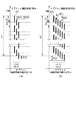
次に、図2のサブアレイ配置により1ショット領域に対して描画を行う態様について説明する。まず、簡単の為、所定方向(ここではY軸方向)にのみ電子線のアレイが複数のサブアレイに分割されているものとして説明を行う。図3は、ショット領域に対してサブアレイで順次描画が行われる複数組の描画領域を例示する図である。同図中、図2におけるものと同一の構成要素には、それと同一の符号を付し、その説明は省略する。まず、Y軸方向におけるサブアレイの幅CYは、Y軸方向におけるサブアレイ200による描画領域(サブアレイ描画領域)の幅301と同じである。各サブアレイの描画領域は、後述の描画方法に従って最初の描画が行われ、ショット領域内のそれぞれ幅301を有する複数の領域(図3の(a)では3つの領域が1列の太線で例示されている)が描画される。ここで、幅SYのスペースの領域には描画は行われない。つづいて、上述のそれぞれ幅301を有する複数の領域を幅CY(第1幅)の[1/n2](図3の(a)では1/n2=1)倍の距離302だけY軸方向にずらし、各サブアレイにより2回目の描画を行う。この2回の描画により、1つのショット領域(幅GY)の描画が完了する。一般的には、幅CYの[1/n2]倍だけY軸方向に順次ずらして得られる[(1+n1/n2)/(1/n2)]=[n1+n2]組のサブアレイ描画領域に対して複数のサブアレイ(サブアレイセット)で順次描画を行うことにより、1つのショット領域の描画が完了する。すなわち、隣接するサブアレイどうしの間隔(CY+SY)を有する部分領域の描画は、幅CYの1/n2倍だけY軸方向に順次ずらして得られる[n1+n2]組のサブアレイ描画領域に対するサブアレイセットによる順次の描画によりなされる。ここで、n2が2以上の場合には、上述のサブアレイ描画領域の各組(図3中、各列の太線で例示される組)は他の組と重なる領域を有し、サブアレイ描画領域の複数の組を順次描画することにより、幅GYのショット領域は、n2回の多重描画により均一な線量で描画されることになる。サブアレイ描画領域の複数の組に対する描画順序は任意でよいが、ステージの副走査方向に沿った順序で順次描画するのがスループット上は好ましい。
Next, a mode in which drawing is performed on one shot area by the subarray arrangement of FIG. First, for the sake of simplicity, the description will be made assuming that the electron beam array is divided into a plurality of subarrays only in a predetermined direction (here, the Y-axis direction). FIG. 3 is a diagram illustrating a plurality of sets of drawing areas in which drawing is sequentially performed on the shot area in the sub-array. In the figure, the same components as those in FIG. 2 are denoted by the same reference numerals, and the description thereof is omitted. First, the width CY of the subarray in the Y-axis direction is the same as the
具体的には、n1/n2=1、かつ、n1=n2=1の場合(図3の(a))、サブアレイ描画領域の組数は、n1+n2=2となり、ずらし量は、CYの[1/n2=1]倍となる。すなわち、CYの1倍だけずれた2組のサブアレイ描画領域に対してサブアレイセットで順次描画を行うことにより、幅GYのショット領域を多重描画することなく(多重度=n2=1(回))均一に描画することができる。 Specifically, when n1 / n2 = 1 and n1 = n2 = 1 ((a) in FIG. 3), the number of sub-array drawing areas is n1 + n2 = 2, and the shift amount is CY [1 / N2 = 1] times. That is, by sequentially drawing with the subarray set with respect to two sets of subarray drawing areas shifted by 1 times CY, the shot area having the width GY is not drawn in a multiple manner (multiplicity = n2 = 1 (times)). It is possible to draw uniformly.
また、n1/n2=1、かつ、n1=n2=2の場合(図3の(b))、サブアレイ描画領域の組数は、n1+n2=4となり、ずらし量は、CYの[1/n2=1/2]倍となる。すなわち、CYの1/2倍だけずれた4組のサブアレイ描画領域に対してサブアレイセットで順次描画を行うことにより、幅GYのショット領域を多重描画(多重度=n2=2(回))で均一に描画することができる。なお、このように描画が多重描画になる場合(n2≧2の場合)、ショット領域の端部に多重度(多重描画回数)の不足する(多重度がn2回未満となる)領域304が幅CYの[1−1/n2]倍の幅で生じる。この領域304の対処方法は後述する。
Further, when n1 / n2 = 1 and n1 = n2 = 2 ((b) of FIG. 3), the number of sub-array drawing areas is n1 + n2 = 4, and the shift amount is CY [1 / n2 = 1/2] times. That is, by sequentially drawing four sub-array drawing areas shifted by ½ times CY in the sub-array set, the shot area having the width GY is drawn with multiple drawing (multiplicity = n2 = 2 (times)). It is possible to draw uniformly. When drawing is multiple drawing (when n2 ≧ 2) as described above, the
図2のような2次元のサブアレイ配置については、Y軸方向にのみ電子線のアレイが複数のサブアレイに分割されているものとして図3を参照し上述した1次元のサブアレイ配置の考え方を拡張すればよい。つまり、サブアレイ描画領域のずらし量は、各軸においてサブアレイの幅の[1/n2]倍となり、サブアレイ描画領域の組数は、各軸での組数(n1+n2)の積となり、多重度は、各軸での多重度(n2)の積となる。例えば、図2のサブアレイ配置でX軸・Y軸ともn1=n2=1の場合、ずらし量は、X軸についてCXの[1/n2=1]倍、Y軸についてCYの[1/n2=1]倍となり、サブアレイ描画領域の組数は、2×2=4となり、多重度は、1×1=1となる。同様に、X軸・Y軸ともn1=n2=2の場合、ずらし量は、X軸についてCXの[1/n2=1/2]倍、Y軸についてCYの[1/n2=1/2]倍となり、サブアレイ描画領域の組数は、4×4=16となり、多重度は、2×2=4となる。同様に、X軸についてn1=n2=1、Y軸についてn1=n2=2の場合、ずらし量は、X軸についてCXの1/n2=1倍、Y軸についてCYの[1/n2=1/2]倍となり、サブアレイ描画領域の組数は、2×4=8となり、多重度は、1×2=2となる。このように、軸によってn1およびn2の少なくとも一方が異なっていてもよい。 For the two-dimensional sub-array arrangement as shown in FIG. 2, it is assumed that the electron beam array is divided into a plurality of sub-arrays only in the Y-axis direction, and the concept of the one-dimensional sub-array arrangement described above with reference to FIG. That's fine. That is, the shift amount of the subarray drawing area is [1 / n2] times the width of the subarray on each axis, the number of subarray drawing areas is the product of the number of sets on each axis (n1 + n2), and the multiplicity is This is the product of multiplicity (n2) on each axis. For example, when n1 = n2 = 1 for both the X axis and the Y axis in the subarray arrangement of FIG. 2, the shift amount is [1 / n2 = 1] times CX for the X axis and [1 / n2 = CY for the Y axis. 1] times, the number of sets of sub-array drawing areas is 2 × 2 = 4, and the multiplicity is 1 × 1 = 1. Similarly, when n1 = n2 = 2 for both the X axis and the Y axis, the shift amount is [1 / n2 = 1/2] times CX for the X axis and [1 / n2 = 1/2 for CY for the Y axis. ], The number of sets of subarray drawing areas is 4 × 4 = 16, and the multiplicity is 2 × 2 = 4. Similarly, when n1 = n2 = 1 for the X axis and n1 = n2 = 2 for the Y axis, the shift amount is 1 / n2 = 1 times CX for the X axis and [1 / n2 = 1 for CY for the Y axis. / 2] times, the number of sets of sub-array drawing areas is 2 × 4 = 8, and the multiplicity is 1 × 2 = 2. Thus, at least one of n1 and n2 may differ with an axis | shaft.
図4は、基板122上の複数のショット領域を描画する態様を例示する図である。X軸方向に幅GX、Y軸方向に幅GYを有するショット領域400を図示の例のように基板122上に隣接させて配列する。そして、1つのショット領域の描画が終了するたびにステージをステップ駆動して、図中矢印で示すような順序で複数のショット領域に対して順次描画を行う。
FIG. 4 is a diagram illustrating an example of drawing a plurality of shot areas on the
図3の(b)で説明したような多重度が不足する(多重度がn2未満となる)領域304に対しては、図4のようにショット領域を隣接して配置することにより、隣接する2つのショットに対する描画が相補的に(補完し合うように)行われる。このような相補的な描画は、隣接するショット領域の存在するショット領域の端部領域については可能であるが、隣接するショット領域の存在しないショット領域の端部領域については不可能であるため、多重度が不足する領域401が残る。よって、このような領域401が基板122に対して設定された有効領域(有効描画領域;基板122の上面の全領域であってもよい)と重ならないように、ショット領域の配列を基板に対して設定するのが好ましい。
As shown in FIG. 3B, the multiplicity insufficient (the multiplicity is less than n2) 304 is adjacent to the
図5は、基板122上におけるサブアレイ内のビーム配置の一例(長方格子配置)を示す図である。同図中、図2における構成要素と同一の構成要素には、それと同一の符号を付し、その説明は省略する。電子線500は、X軸方向にピッチPx、Y軸方向にピッチPyをもって、格子状に配列されている。この複数の電子線による描画は、X軸方向における主として偏向器アレイ120による電子線の偏向(ピッチPxにわたるラスタスキャン;主走査)と、Y軸方向における主としてステージの移動(ピッチPyにわたるスキャン;副走査)とによりなされる。電子線のピッチは可能な限り小さくしたいが、アパーチャアレイ116および静電レンズアレイ117・121の機械的設計制約や光学的設計制約等により、通常数十μm程度は必要となる。一方、偏向器アレイ120による電子線の基板上での偏向量は、許容できる偏向収差等の要因から、電子線のピッチより小さい数μm程度に制限される。その為、X軸方向に領域を分割し、上述のラスタスキャンをX軸方向に分割された領域ごとに行うことになる。各サブアレイ描画領域に対する描画の中で多重描画がなされるようにしてもよい。なお、X軸方向を主走査方向、Y軸方向を副走査方向としたが、逆であってもよい。
FIG. 5 is a diagram illustrating an example of beam arrangement (rectangular lattice arrangement) in the sub-array on the
図6は、基板122上におけるサブアレイ内のビーム配置の一例(千鳥格子配置)を示す図である。同図中、図2における構成要素と同一の構成要素には、それと同一の符号を付し、その説明は省略する。荷電粒子線600は、X軸方向にピッチPcx、Y軸方向にピッチPcyをもって配列され、また、ピッチPcyだけ隔たった隣接する2つの行の間では、電子線がX軸方向に距離Dxだけずれて配列されており、いわゆる千鳥格子状の配列となっている。換言すれば、X軸方向に延びる電子線の配列(行)をY軸方向にピッチPcy、X軸方向に距離Dxずつ順次ずらして配列することにより得られる配列となっている。距離Dxは、ピッチPcxの[1/k]倍の距離(kは2以上の整数)を選択するのが好ましい。その場合、1行における電子線の位置は、(Pcx/Dx)行を1周期として繰り返されることになる。この1周期に対応するY軸方向の幅Pcを有する電子線の束を1千鳥ブロックと呼ぶことにすると、本実施形態では、Y軸方向に並ぶ複数の千鳥ブロックをもって1つのサブアレイを構成している。図4では、1千鳥ブロックが4行の電子線で構成されている例を示しているが、1千鳥ブロックを構成する電子線の行数はその限りではない。
FIG. 6 is a diagram illustrating an example of the beam arrangement in the sub-array on the substrate 122 (houndstooth arrangement). In the figure, the same components as those in FIG. 2 are denoted by the same reference numerals, and the description thereof is omitted. The charged
そのように配列された複数の電子線による描画は、X軸方向における主として偏向器アレイ120による電子線の偏向(幅Dxにわたるラスタスキャン;主走査)と、Y軸方向における主としてステージの移動(幅Pcにわたるスキャン;副走査)とによりなされる。幅Dxは、偏向器アレイ120の偏向幅以下の値にするのが好ましい。そうすれば、上述したようなX軸方向における領域分割とその順次描画とが不要となり、Y軸方向におけるステージの移動(副走査)の回数の少なさ(スループット)の点で有利となる。
Drawing with a plurality of electron beams arranged in such a way is mainly deflection of the electron beam by the
なお、各サブアレイ描画領域に対する描画の中で多重描画がなされるようにしてもよい。図6の1千鳥ブロックのようなサブアレイより小さい電子線のブロックをY軸方向に複数配列してサブアレイが構成されている場合、その繰り返し性を利用して多重描画を行ってもよい。具体的には、例えば、Y軸方向におけるステージの移動(副走査)を1千鳥ブロックの幅PcのM倍の幅だけ行うことにより、M回の多重描画を行うことができる。Y軸方向に並べた千鳥ブロックの個数と多重度Mとを一致させるのが好ましい。そのようにすれば、ステージをステップ動作させることなく、隣接し合う複数のサブアレイ描画領域に対して連続的なスキャン動作(副走査)で描画を行うことができ、スループットの点で有利である。 Note that multiple drawing may be performed during drawing for each sub-array drawing region. When a plurality of electron beam blocks smaller than the sub-array such as the 1 staggered block in FIG. 6 are arranged in the Y-axis direction, the sub-array may be formed by using the repeatability. Specifically, for example, by performing stage movement (sub-scanning) in the Y-axis direction by a width that is M times the width Pc of the staggered block, M multiple drawing can be performed. It is preferable to match the number of zigzag blocks arranged in the Y-axis direction with the multiplicity M. By doing so, it is possible to perform drawing in a continuous scanning operation (sub-scanning) for a plurality of adjacent sub-array drawing regions without stepping the stage, which is advantageous in terms of throughput.
なお、上述のような千鳥格子配置のサブアレイを用いた場合、各サブアレイ描画領域は、Y軸方向に延びる境界(外縁)において1千鳥ブロックのY軸方向の幅Pcに対応した幅の形状を連ねた鋸歯状の境界を有することになる。また、上述した千鳥ブロックの繰り返し性を利用した多重描画の場合、Y軸方向において幅Pcの(M−1)倍の幅で多重度が不足する(多重度がM未満)の領域がショット領域内に生じる。当該領域については、基板122上の複数のショット領域を描画する図4を参照して説明した態様と同様に複数のショット領域を隣接させて配列し順次描画することにより、他の領域と同様の多重度とすることができる。なお、X軸方向を主走査方向、Y軸方向を副走査方向としたが、逆であってもよい。
When the above-described subarray with the staggered lattice arrangement is used, each subarray drawing area has a shape corresponding to the width Pc in the Y-axis direction of the staggered block at the boundary (outer edge) extending in the Y-axis direction. It will have a continuous serrated boundary. Further, in the case of multiple drawing using the above-described repeatability of the staggered block, an area where the multiplicity is insufficient (the multiplicity is less than M) is (M−1) times the width Pc in the Y-axis direction. Occurs within. As for the area, the plurality of shot areas are arranged adjacent to each other in the same manner as described with reference to FIG. 4 in which a plurality of shot areas on the
本実施形態によれば、サブアレイの荷電粒子線を有効に利用するのに有利な描画装置を提供することができる。 According to this embodiment, it is possible to provide a drawing apparatus that is advantageous for effectively using the charged particle beam of the subarray.
[実施形態2]
図7は、本実施形態に係るサブアレイの別の配置例を示す図である。図7は、基板122上での電子線のサブアレイの配置を示している。同図中、図2の構成要素と同一の構成要素には、それと同一の符号を付し、その説明は省略する。実施形態1の構成とは異なる点に関して説明する。図7は、n1/n2=1/2の場合を示している。実施形態1(図2)との違いは、サブアレイ間のスペースの幅がサブアレイの幅より狭いことである。ここでは、SX=CX/2、SY=CY/2を満たすようにサブアレイが配列されている。n1/n2<1を満たす場合、実施形態1(n1/n2=1)の構成例と比較して、アパーチャアレイ116の開口率が高く、電子線源からの電子線の利用効率が高いことになる。この場合、例えば、電子線アレイにおける電子線の本数を増加させることができる。また、この場合、電子線アレイにおける電子線の本数を同じとすれば、サブアレイ描画領域(画角、または、アパーチャアレイ116において開口が配列されている範囲)が狭くなり、電子線源に要求されるエミッタンスを低減させることができる。この点で、n1/n2<1を満たすサブアレイ配置の構成は好ましいといえる。
[Embodiment 2]
FIG. 7 is a diagram illustrating another arrangement example of the subarrays according to the present embodiment. FIG. 7 shows an arrangement of electron beam sub-arrays on the
図7のサブアレイ配置により1ショット領域に対して描画を行う態様について、実施形態1の場合と同様の方法で説明を行う。図8は、ショット領域に対してサブアレイのセットで順次描画が行われる複数組の描画領域を例示する図である。同図中、図2・図3の構成要素と同一の構成要素には、それと同一の符号を付し、その説明は省略する。まず、n1/n2=1/2、かつ、n1=1、n2=2の場合(図8の(a))、サブアレイ描画領域の組数は、n1+n2=3となり、ずらし量は、CYの[1/n2=1/2]倍となる。すなわち、CYの1/2倍ずつずれた3組のサブアレイ描画領域に対してサブアレイセットで順次描画を行うことにより、幅GYのショット領域を多重描画により(多重度=n2=2(回))均一に描画することができる。また、n1/n2=1/2、かつ、n1=2、n2=4の場合(図8の(b))、サブアレイ描画領域の組数は、n1+n2=6となり、ずらし量は、CYの[1/n2=1/4]倍となる。すなわち、CYの1/4倍ずつずれた4組のサブアレイ描画領域に対してサブアレイセットで順次描画を行うことにより、幅GYのショット領域を多重描画により(多重度=n2=4(回))均一に描画することができる。なお、本実施形態における描画は多重描画になる(n2≧2)ため、ショット領域の端部に多重度(多重描画回数)の不足する(多重度がn2回未満となる)領域802が幅CYの[1−1/n2]倍の幅で生じる。当該領域については、基板122上の複数のショット領域を描画する図4を参照して説明した態様と同様に複数のショット領域を隣接させて配列し順次描画することにより、他の領域と同様の多重度とすることができる。
An aspect in which drawing is performed on one shot area by the subarray arrangement of FIG. 7 will be described in the same manner as in the first embodiment. FIG. 8 is a diagram illustrating a plurality of sets of drawing areas in which drawing is sequentially performed on a shot area by a set of subarrays. In the figure, the same components as those in FIGS. 2 and 3 are denoted by the same reference numerals, and description thereof is omitted. First, when n1 / n2 = 1/2, n1 = 1, and n2 = 2 ((a) in FIG. 8), the number of sub-array drawing areas is n1 + n2 = 3, and the shift amount is CY [ 1 / n2 = 1/2] times. That is, by sequentially drawing three sets of sub-array drawing regions shifted by ½ times CY in the sub-array set, the shot region having the width GY is subjected to multiple drawing (multiplicity = n2 = 2 (times)). It is possible to draw uniformly. When n1 / n2 = 1/2, n1 = 2, and n2 = 4 (FIG. 8B), the number of sub-array drawing areas is n1 + n2 = 6, and the shift amount is CY [ 1 / n2 = 1/4] times. That is, by sequentially drawing with four sub-array drawing areas shifted by 1/4 times of CY in the sub-array set, the shot area with the width GY is subjected to multiple drawing (multiplicity = n2 = 4 (times)). It is possible to draw uniformly. Since the drawing in the present embodiment is multiple drawing (n2 ≧ 2), the
本実施形態によれば、サブアレイの荷電粒子線を有効に利用するのに有利な描画装置を提供することができる。 According to this embodiment, it is possible to provide a drawing apparatus that is advantageous for effectively using the charged particle beam of the subarray.
[実施形態3]
本発明の実施形態に係る物品の製造方法は、例えば、半導体デバイス等のマイクロデバイスや微細構造を有する素子等の物品を製造するのに好適である。該製造方法は、感光剤が塗布された基板の該感光剤に上記の描画装置を用いて潜像パターンを形成する工程(基板に描画を行う工程)と、当該工程で潜像パターンが形成された基板を現像する工程とを含みうる。さらに、該製造方法は、他の周知の工程(酸化、成膜、蒸着、ドーピング、平坦化、エッチング、レジスト剥離、ダイシング、ボンディング、パッケージング等)を含みうる。本実施形態の物品の製造方法は、従来の方法に比べて、物品の性能・品質・生産性・生産コストの少なくとも1つにおいて有利である。
[Embodiment 3]
The method for manufacturing an article according to an embodiment of the present invention is suitable for manufacturing an article such as a microdevice such as a semiconductor device or an element having a fine structure. The manufacturing method includes a step of forming a latent image pattern on the photosensitive agent on the substrate coated with the photosensitive agent using the above drawing apparatus (a step of drawing on the substrate), and the latent image pattern is formed in the step. Developing the substrate. Further, the manufacturing method may include other well-known steps (oxidation, film formation, vapor deposition, doping, planarization, etching, resist stripping, dicing, bonding, packaging, and the like). The method for manufacturing an article according to the present embodiment is advantageous in at least one of the performance, quality, productivity, and production cost of the article as compared with the conventional method.
以上、本発明の実施形態について説明したが、本発明はこれらの実施形態に限定されず、その要旨の範囲内で種々の変形および変更が可能である。 As mentioned above, although embodiment of this invention was described, this invention is not limited to these embodiment, A various deformation | transformation and change are possible within the range of the summary.
123 ステージ部(ステージおよび駆動手段)
COS 投射系
100 コントローラー(制御手段)
123 Stage part (stage and drive means)
Claims (6)
前記基板を保持するステージと、
前記ステージに保持された基板に前記アレイを投射する投射系と、
前記基板上の描画領域を変更するように前記ステージと前記投射系との間の所定方向における相対移動を行わせる駆動手段と、
制御手段と、を有し、
前記投射系は、
前記アレイは、前記基板上において、前記所定方向にスペースをもって離散的に配列された複数のサブアレイを含み、かつ、
前記所定方向における前記スペースの幅(第2幅)は、前記所定方向における前記サブアレイの幅(第1幅)の[n1/n2]倍(n1、n2は正の整数、かつn2は2以上)となる、ように構成され、
前記制御手段は、前記第1幅の[1/n2]倍ずつ前記所定方向にずれている[n1+n2]組の描画領域に前記複数のサブアレイのうちの対応するサブアレイで順次描画が行われてn2を多重度とする描画がなされるように、前記投射系と前記駆動手段とを制御し、
前記投射系は、n1/n2<1を満たすように構成されている、
ことを特徴とする描画装置。 A drawing apparatus for drawing on a substrate with an array of charged particle beams,
A stage for holding the substrate;
A projection system for projecting the array onto a substrate held on the stage;
Driving means for performing relative movement in a predetermined direction between the stage and the projection system so as to change a drawing area on the substrate;
Control means, and
The projection system is
The array includes a plurality of subarrays arranged discretely with a space in the predetermined direction on the substrate; and
The width (second width) of the space in the predetermined direction is [n1 / n2] times the width (first width) of the subarray in the predetermined direction (n1, n2 are positive integers, and n2 is 2 or more). Configured to be
Said control means, said are offset [1 / n2] times by the predetermined direction of the first width [n1 + n2] of sets of sequential rendering been conducted with in the corresponding sub-array of the plurality of sub-arrays in the drawing area n2 the so drawing to multiplicity is the main, by controlling the said drive means and said projection system,
The projection system is configured to satisfy n1 / n2 <1.
A drawing apparatus characterized by that.
前記複数のショット領域の配列は、隣接するショット領域の存在しないショット領域の端部領域であって前記多重描画の多重度が不足する端部領域が、前記基板に対して設定された有効領域と重ならないように、前記基板に対して設定されている、
ことを特徴とする請求項1乃至請求項4のいずれか1項に記載の描画装置。 The control means controls the projection system and the driving means so that drawing is sequentially performed on a plurality of shot areas arranged adjacent to each other on the substrate,
The arrangement of the plurality of shot areas is an end area of a shot area where there is no adjacent shot area, and an end area where the multiplicity of the multiple drawing is insufficient is an effective area set for the substrate Set to the board so as not to overlap,
The drawing apparatus according to any one of claims 1 to 4 , wherein the drawing apparatus is characterized in that:
前記工程で描画を行われた基板を現像する工程と、
を含むことを特徴とする物品の製造方法。 Drawing on a substrate using the drawing apparatus according to any one of claims 1 to 5 ,
Developing the substrate on which the drawing has been performed in the step;
A method for producing an article comprising:
Priority Applications (2)
| Application Number | Priority Date | Filing Date | Title |
|---|---|---|---|
| JP2010244366A JP5709465B2 (en) | 2010-10-29 | 2010-10-29 | Drawing apparatus and article manufacturing method |
| US13/281,797 US20120107748A1 (en) | 2010-10-29 | 2011-10-26 | Drawing apparatus and method of manufacturing article |
Applications Claiming Priority (1)
| Application Number | Priority Date | Filing Date | Title |
|---|---|---|---|
| JP2010244366A JP5709465B2 (en) | 2010-10-29 | 2010-10-29 | Drawing apparatus and article manufacturing method |
Publications (3)
| Publication Number | Publication Date |
|---|---|
| JP2012099568A JP2012099568A (en) | 2012-05-24 |
| JP2012099568A5 JP2012099568A5 (en) | 2013-12-12 |
| JP5709465B2 true JP5709465B2 (en) | 2015-04-30 |
Family
ID=45997143
Family Applications (1)
| Application Number | Title | Priority Date | Filing Date |
|---|---|---|---|
| JP2010244366A Expired - Fee Related JP5709465B2 (en) | 2010-10-29 | 2010-10-29 | Drawing apparatus and article manufacturing method |
Country Status (2)
| Country | Link |
|---|---|
| US (1) | US20120107748A1 (en) |
| JP (1) | JP5709465B2 (en) |
Families Citing this family (3)
| Publication number | Priority date | Publication date | Assignee | Title |
|---|---|---|---|---|
| JP2013069813A (en) * | 2011-09-21 | 2013-04-18 | Canon Inc | Drawing device and method of manufacturing article |
| JP6195349B2 (en) * | 2013-04-26 | 2017-09-13 | キヤノン株式会社 | Drawing apparatus, drawing method, and article manufacturing method |
| DE102019005362A1 (en) * | 2019-07-31 | 2021-02-04 | Carl Zeiss Multisem Gmbh | Method for operating a multitude particle beam system with changing the numerical aperture, associated computer program product and multitude particle beam system |
Family Cites Families (16)
| Publication number | Priority date | Publication date | Assignee | Title |
|---|---|---|---|---|
| JPH038321A (en) * | 1989-06-06 | 1991-01-16 | Mitsubishi Electric Corp | Lithography for minute width pattern |
| KR950002578B1 (en) * | 1991-03-13 | 1995-03-23 | 후지쓰 가부시끼가이샤 | Charged particle beam exposure system and charged particle beam exposure method |
| JP3518097B2 (en) * | 1995-09-29 | 2004-04-12 | 株式会社ニコン | Charged particle beam transfer device, pattern division method, mask, and charged particle beam transfer method |
| JP3647128B2 (en) * | 1996-03-04 | 2005-05-11 | キヤノン株式会社 | Electron beam exposure apparatus and exposure method thereof |
| JP3457474B2 (en) * | 1996-07-17 | 2003-10-20 | 株式会社東芝 | Charged beam drawing equipment |
| US6175122B1 (en) * | 1998-01-09 | 2001-01-16 | International Business Machines Corporation | Method for writing a pattern using multiple variable shaped electron beams |
| JPH11307445A (en) * | 1998-04-23 | 1999-11-05 | Nikon Corp | Charged particle beam exposure system and its projection mask |
| US6768124B2 (en) * | 1999-10-19 | 2004-07-27 | Nikon Corporation | Reticle-focus detector, and charged-particle-beam microlithography apparatus and methods comprising same |
| AU2001255614A1 (en) * | 2000-06-01 | 2001-12-11 | Applied Materials, Inc. | High throughput multipass printing with lithographic quality |
| EP1273907A4 (en) * | 2000-11-17 | 2006-08-30 | Ebara Corp | Wafer inspecting method, wafer inspecting instrument, and electron beam apparatus |
| US7061581B1 (en) * | 2004-11-22 | 2006-06-13 | Asml Netherlands B.V. | Lithographic apparatus and device manufacturing method |
| US7126672B2 (en) * | 2004-12-27 | 2006-10-24 | Asml Netherlands B.V. | Lithographic apparatus and device manufacturing method |
| US7468506B2 (en) * | 2005-01-26 | 2008-12-23 | Applied Materials, Israel, Ltd. | Spot grid array scanning system |
| JP4378648B2 (en) * | 2006-10-06 | 2009-12-09 | エルピーダメモリ株式会社 | Irradiation pattern data creation method, mask manufacturing method, and drawing system |
| CN104795303B (en) * | 2009-05-20 | 2017-12-05 | 迈普尔平版印刷Ip有限公司 | Method for pattern Processing data |
| JP6128744B2 (en) * | 2012-04-04 | 2017-05-17 | キヤノン株式会社 | Drawing apparatus, drawing method, and article manufacturing method |
-
2010
- 2010-10-29 JP JP2010244366A patent/JP5709465B2/en not_active Expired - Fee Related
-
2011
- 2011-10-26 US US13/281,797 patent/US20120107748A1/en not_active Abandoned
Also Published As
| Publication number | Publication date |
|---|---|
| US20120107748A1 (en) | 2012-05-03 |
| JP2012099568A (en) | 2012-05-24 |
Similar Documents
| Publication | Publication Date | Title |
|---|---|---|
| JP6264613B2 (en) | Method for charged particle multi-beam exposure | |
| KR101647768B1 (en) | Method of and system for exposing a target | |
| JP4576432B2 (en) | Use of multi-beam modulators for particle beams and multi-beam modulators for maskless structuring of substrates | |
| JP6195349B2 (en) | Drawing apparatus, drawing method, and article manufacturing method | |
| JP2016178300A (en) | Multi-beam drawing by bidirectional double path system | |
| KR101698890B1 (en) | Multi charged particle beam blankiing device and multi charged particle beam drawing device | |
| JP2019071411A (en) | Method for irradiating target using restricted placement grid | |
| JP7106353B2 (en) | Multi-charged particle beam inspection device and multi-charged particle beam inspection method | |
| JP5709465B2 (en) | Drawing apparatus and article manufacturing method | |
| JP6087570B2 (en) | Drawing apparatus and article manufacturing method | |
| JP2013128031A (en) | Multiple charged particle beam lithography apparatus and multiple charged particle beam lithography method | |
| US8927945B2 (en) | Drawing apparatus and method of manufacturing article by controlling drawing on shot region side of boundary of shot regions | |
| US9001387B2 (en) | Drawing apparatus, data processing method, and method of manufacturing article that transform partially overlapping regions using different transformation rules | |
| JP6193611B2 (en) | Drawing apparatus and article manufacturing method | |
| US20130344443A1 (en) | Lithography apparatus, and method of manufacture of product | |
| JP3913250B2 (en) | Electron beam exposure apparatus and exposure method therefor | |
| JP2015035563A (en) | Drawing data generation method, processing device, program, drawing device and article manufacturing method | |
| JP3976835B2 (en) | Electron beam exposure method and electron beam exposure apparatus | |
| JP2016092136A (en) | Drawing device, and method of manufacturing article | |
| JP2016062939A (en) | Drawing device and drawing method, and method of manufacturing article | |
| TWI460548B (en) | Method of and system for exposing a target | |
| TW202316468A (en) | Charged-particle optical device | |
| JP4804592B2 (en) | Charged particle beam apparatus and device manufacturing method | |
| JP2004153294A (en) | Electron beam exposure device, electron beam exposure method and device manufacturing method | |
| EP3651183B1 (en) | Beam grid layout |
Legal Events
| Date | Code | Title | Description |
|---|---|---|---|
| A521 | Written amendment |
Free format text: JAPANESE INTERMEDIATE CODE: A523 Effective date: 20131029 |
|
| A621 | Written request for application examination |
Free format text: JAPANESE INTERMEDIATE CODE: A621 Effective date: 20131029 |
|
| A977 | Report on retrieval |
Free format text: JAPANESE INTERMEDIATE CODE: A971007 Effective date: 20140617 |
|
| A131 | Notification of reasons for refusal |
Free format text: JAPANESE INTERMEDIATE CODE: A131 Effective date: 20140701 |
|
| A521 | Written amendment |
Free format text: JAPANESE INTERMEDIATE CODE: A523 Effective date: 20140822 |
|
| TRDD | Decision of grant or rejection written | ||
| A01 | Written decision to grant a patent or to grant a registration (utility model) |
Free format text: JAPANESE INTERMEDIATE CODE: A01 Effective date: 20150203 |
|
| A61 | First payment of annual fees (during grant procedure) |
Free format text: JAPANESE INTERMEDIATE CODE: A61 Effective date: 20150303 |
|
| LAPS | Cancellation because of no payment of annual fees |