JP5696367B2 - Semiconductor device and manufacturing method thereof - Google Patents
Semiconductor device and manufacturing method thereof Download PDFInfo
- Publication number
- JP5696367B2 JP5696367B2 JP2010076592A JP2010076592A JP5696367B2 JP 5696367 B2 JP5696367 B2 JP 5696367B2 JP 2010076592 A JP2010076592 A JP 2010076592A JP 2010076592 A JP2010076592 A JP 2010076592A JP 5696367 B2 JP5696367 B2 JP 5696367B2
- Authority
- JP
- Japan
- Prior art keywords
- semiconductor element
- electrode pad
- connection terminal
- wire
- electrode
- Prior art date
- Legal status (The legal status is an assumption and is not a legal conclusion. Google has not performed a legal analysis and makes no representation as to the accuracy of the status listed.)
- Expired - Fee Related
Links
Images


Classifications
-
- H—ELECTRICITY
- H01—ELECTRIC ELEMENTS
- H01L—SEMICONDUCTOR DEVICES NOT COVERED BY CLASS H10
- H01L24/00—Arrangements for connecting or disconnecting semiconductor or solid-state bodies; Methods or apparatus related thereto
- H01L24/01—Means for bonding being attached to, or being formed on, the surface to be connected, e.g. chip-to-package, die-attach, "first-level" interconnects; Manufacturing methods related thereto
- H01L24/02—Bonding areas ; Manufacturing methods related thereto
- H01L24/04—Structure, shape, material or disposition of the bonding areas prior to the connecting process
- H01L24/05—Structure, shape, material or disposition of the bonding areas prior to the connecting process of an individual bonding area
-
- H—ELECTRICITY
- H01—ELECTRIC ELEMENTS
- H01L—SEMICONDUCTOR DEVICES NOT COVERED BY CLASS H10
- H01L2224/00—Indexing scheme for arrangements for connecting or disconnecting semiconductor or solid-state bodies and methods related thereto as covered by H01L24/00
- H01L2224/01—Means for bonding being attached to, or being formed on, the surface to be connected, e.g. chip-to-package, die-attach, "first-level" interconnects; Manufacturing methods related thereto
- H01L2224/02—Bonding areas; Manufacturing methods related thereto
- H01L2224/04—Structure, shape, material or disposition of the bonding areas prior to the connecting process
- H01L2224/04042—Bonding areas specifically adapted for wire connectors, e.g. wirebond pads
-
- H—ELECTRICITY
- H01—ELECTRIC ELEMENTS
- H01L—SEMICONDUCTOR DEVICES NOT COVERED BY CLASS H10
- H01L2224/00—Indexing scheme for arrangements for connecting or disconnecting semiconductor or solid-state bodies and methods related thereto as covered by H01L24/00
- H01L2224/01—Means for bonding being attached to, or being formed on, the surface to be connected, e.g. chip-to-package, die-attach, "first-level" interconnects; Manufacturing methods related thereto
- H01L2224/42—Wire connectors; Manufacturing methods related thereto
- H01L2224/47—Structure, shape, material or disposition of the wire connectors after the connecting process
- H01L2224/48—Structure, shape, material or disposition of the wire connectors after the connecting process of an individual wire connector
- H01L2224/484—Connecting portions
- H01L2224/48463—Connecting portions the connecting portion on the bonding area of the semiconductor or solid-state body being a ball bond
- H01L2224/48465—Connecting portions the connecting portion on the bonding area of the semiconductor or solid-state body being a ball bond the other connecting portion not on the bonding area being a wedge bond, i.e. ball-to-wedge, regular stitch
-
- H—ELECTRICITY
- H01—ELECTRIC ELEMENTS
- H01L—SEMICONDUCTOR DEVICES NOT COVERED BY CLASS H10
- H01L2224/00—Indexing scheme for arrangements for connecting or disconnecting semiconductor or solid-state bodies and methods related thereto as covered by H01L24/00
- H01L2224/01—Means for bonding being attached to, or being formed on, the surface to be connected, e.g. chip-to-package, die-attach, "first-level" interconnects; Manufacturing methods related thereto
- H01L2224/42—Wire connectors; Manufacturing methods related thereto
- H01L2224/47—Structure, shape, material or disposition of the wire connectors after the connecting process
- H01L2224/49—Structure, shape, material or disposition of the wire connectors after the connecting process of a plurality of wire connectors
- H01L2224/491—Disposition
- H01L2224/4912—Layout
- H01L2224/49175—Parallel arrangements
-
- H—ELECTRICITY
- H01—ELECTRIC ELEMENTS
- H01L—SEMICONDUCTOR DEVICES NOT COVERED BY CLASS H10
- H01L2224/00—Indexing scheme for arrangements for connecting or disconnecting semiconductor or solid-state bodies and methods related thereto as covered by H01L24/00
- H01L2224/73—Means for bonding being of different types provided for in two or more of groups H01L2224/10, H01L2224/18, H01L2224/26, H01L2224/34, H01L2224/42, H01L2224/50, H01L2224/63, H01L2224/71
- H01L2224/732—Location after the connecting process
- H01L2224/73201—Location after the connecting process on the same surface
- H01L2224/73203—Bump and layer connectors
-
- H—ELECTRICITY
- H01—ELECTRIC ELEMENTS
- H01L—SEMICONDUCTOR DEVICES NOT COVERED BY CLASS H10
- H01L2224/00—Indexing scheme for arrangements for connecting or disconnecting semiconductor or solid-state bodies and methods related thereto as covered by H01L24/00
- H01L2224/73—Means for bonding being of different types provided for in two or more of groups H01L2224/10, H01L2224/18, H01L2224/26, H01L2224/34, H01L2224/42, H01L2224/50, H01L2224/63, H01L2224/71
- H01L2224/732—Location after the connecting process
- H01L2224/73201—Location after the connecting process on the same surface
- H01L2224/73207—Bump and wire connectors
-
- H—ELECTRICITY
- H01—ELECTRIC ELEMENTS
- H01L—SEMICONDUCTOR DEVICES NOT COVERED BY CLASS H10
- H01L2924/00—Indexing scheme for arrangements or methods for connecting or disconnecting semiconductor or solid-state bodies as covered by H01L24/00
- H01L2924/0001—Technical content checked by a classifier
- H01L2924/00014—Technical content checked by a classifier the subject-matter covered by the group, the symbol of which is combined with the symbol of this group, being disclosed without further technical details
-
- H—ELECTRICITY
- H01—ELECTRIC ELEMENTS
- H01L—SEMICONDUCTOR DEVICES NOT COVERED BY CLASS H10
- H01L2924/00—Indexing scheme for arrangements or methods for connecting or disconnecting semiconductor or solid-state bodies as covered by H01L24/00
- H01L2924/01—Chemical elements
- H01L2924/01004—Beryllium [Be]
-
- H—ELECTRICITY
- H01—ELECTRIC ELEMENTS
- H01L—SEMICONDUCTOR DEVICES NOT COVERED BY CLASS H10
- H01L2924/00—Indexing scheme for arrangements or methods for connecting or disconnecting semiconductor or solid-state bodies as covered by H01L24/00
- H01L2924/01—Chemical elements
- H01L2924/01006—Carbon [C]
-
- H—ELECTRICITY
- H01—ELECTRIC ELEMENTS
- H01L—SEMICONDUCTOR DEVICES NOT COVERED BY CLASS H10
- H01L2924/00—Indexing scheme for arrangements or methods for connecting or disconnecting semiconductor or solid-state bodies as covered by H01L24/00
- H01L2924/01—Chemical elements
- H01L2924/01013—Aluminum [Al]
-
- H—ELECTRICITY
- H01—ELECTRIC ELEMENTS
- H01L—SEMICONDUCTOR DEVICES NOT COVERED BY CLASS H10
- H01L2924/00—Indexing scheme for arrangements or methods for connecting or disconnecting semiconductor or solid-state bodies as covered by H01L24/00
- H01L2924/01—Chemical elements
- H01L2924/01029—Copper [Cu]
-
- H—ELECTRICITY
- H01—ELECTRIC ELEMENTS
- H01L—SEMICONDUCTOR DEVICES NOT COVERED BY CLASS H10
- H01L2924/00—Indexing scheme for arrangements or methods for connecting or disconnecting semiconductor or solid-state bodies as covered by H01L24/00
- H01L2924/01—Chemical elements
- H01L2924/01033—Arsenic [As]
-
- H—ELECTRICITY
- H01—ELECTRIC ELEMENTS
- H01L—SEMICONDUCTOR DEVICES NOT COVERED BY CLASS H10
- H01L2924/00—Indexing scheme for arrangements or methods for connecting or disconnecting semiconductor or solid-state bodies as covered by H01L24/00
- H01L2924/01—Chemical elements
- H01L2924/0105—Tin [Sn]
-
- H—ELECTRICITY
- H01—ELECTRIC ELEMENTS
- H01L—SEMICONDUCTOR DEVICES NOT COVERED BY CLASS H10
- H01L2924/00—Indexing scheme for arrangements or methods for connecting or disconnecting semiconductor or solid-state bodies as covered by H01L24/00
- H01L2924/01—Chemical elements
- H01L2924/01067—Holmium [Ho]
-
- H—ELECTRICITY
- H01—ELECTRIC ELEMENTS
- H01L—SEMICONDUCTOR DEVICES NOT COVERED BY CLASS H10
- H01L2924/00—Indexing scheme for arrangements or methods for connecting or disconnecting semiconductor or solid-state bodies as covered by H01L24/00
- H01L2924/01—Chemical elements
- H01L2924/01074—Tungsten [W]
-
- H—ELECTRICITY
- H01—ELECTRIC ELEMENTS
- H01L—SEMICONDUCTOR DEVICES NOT COVERED BY CLASS H10
- H01L2924/00—Indexing scheme for arrangements or methods for connecting or disconnecting semiconductor or solid-state bodies as covered by H01L24/00
- H01L2924/01—Chemical elements
- H01L2924/01078—Platinum [Pt]
-
- H—ELECTRICITY
- H01—ELECTRIC ELEMENTS
- H01L—SEMICONDUCTOR DEVICES NOT COVERED BY CLASS H10
- H01L2924/00—Indexing scheme for arrangements or methods for connecting or disconnecting semiconductor or solid-state bodies as covered by H01L24/00
- H01L2924/01—Chemical elements
- H01L2924/01079—Gold [Au]
-
- H—ELECTRICITY
- H01—ELECTRIC ELEMENTS
- H01L—SEMICONDUCTOR DEVICES NOT COVERED BY CLASS H10
- H01L2924/00—Indexing scheme for arrangements or methods for connecting or disconnecting semiconductor or solid-state bodies as covered by H01L24/00
- H01L2924/013—Alloys
- H01L2924/014—Solder alloys
Description
本発明は、半導体装置及びその製造方法に関する。 The present invention relates to a semiconductor device and a manufacturing method thereof.
近年、半導体装置の大集積化、及び処理の高速化が図られており、これに伴って、複数の半導体素子を3次元に配列したパッケージが開発されている。
半導体素子同士の接続は、半導体素子に形成した端子を用いる場合には、フリップチップ接続が用いられる。また、外部の電極と半導体素子の接続には、ワイヤボンディングが用いられる。
In recent years, semiconductor devices have been highly integrated and the processing speed has been increased, and accordingly, a package in which a plurality of semiconductor elements are arranged three-dimensionally has been developed.
For the connection between the semiconductor elements, flip-chip connection is used when a terminal formed in the semiconductor element is used. Wire bonding is used to connect the external electrode and the semiconductor element.
ここで、回路基板の上に半導体素子を2つ重ねて実装するときは、最初に回路基板の上に第1の半導体素子を実装し、さらに第1の半導体素子の上にインターポーザを実装してから、第2の半導体素子を実装することが知られている。
図11に示すように、従来の半導体装置101では、回路基板102の上に第1の半導体素子103をアップフェイスで実装し、第1の半導体素子103の上に、ハンダバンプ111を介してインターポーザ104を接続する。さらに、インターポーザ104の上にハンダバンプ112を介して第2の半導体素子105を実装していた。
Here, when two semiconductor elements are mounted on the circuit board, the first semiconductor element is first mounted on the circuit board, and the interposer is further mounted on the first semiconductor element. Therefore, it is known to mount a second semiconductor element.
As shown in FIG. 11, in the
インターポーザ104の両面には、第1、第2の半導体素子103、105に電気的に接続される電極パッド109a,109bが形成されている。さらに、これら電極パッド109a,109bを導通させるための導電性プラグ110がインターポーザ104を貫通している。また、インターポーザ104は、第2の半導体素子105よりサイズの大きいものが用いられ、インターポーザ104の周縁部分であって、第2の半導体素子105から露出する部分には、外部接続用の電極106が形成されている。
この半導体装置101では、第2の半導体素子105と第1の半導体素子103とがインターポーザ104の電極パッド109a,109b及び導電性プラグ110並びにハンダバンプ111,112を介して電気的に接続される。さらに、電極106がワイヤ107を介して回路基板102側の基板電極108に接続される。これにより、第1の半導体素子103又は第2の半導体素子105が、インターポーザ104を介して回路基板102に電気的に接続される。
In the
しかしながら、従来の半導体装置101では、第1の半導体素子103の上にインターポーザ104を実装する工程が必要になるため、製造時間を短縮することができなかった。また、インターポーザ104に電極106や図示を省略する配線を形成する必要があるので、製造コストが増加していた。
However, in the
ここで、従来の半導体装置101で、インターポーザ104を使用せずに、第1の半導
体素子103の上に第2の半導体素子105を実装する場合、第1の半導体素子103が第2の半導体素子105より大きければ、第1の半導体素子103の周縁部分を使用して、第1の半導体素子103と回路基板102とをワイヤ107で電気的に接続することができる。しかしながら、図12に示すように、第1の半導体素子103の大きさが第2の半導体素子105の大きさ以下であると、第1の半導体素子103が第2の半導体素子105で覆われてしまい。ワイヤ107を通すスペースが得られなくなる。
本発明は、このような事情に鑑みてなされたものであり、複数の半導体素子を積層させる半導体装置を低コストで用意に製造できるようにすることを目的とする。
Here, in the
The present invention has been made in view of such circumstances, and an object of the present invention is to enable a semiconductor device in which a plurality of semiconductor elements are stacked to be easily prepared at low cost.
本願の一観点によれば、基板と、前記基板にフェイスアップで実装され、第1の電極パッドと第2の電極パッドが設けられた第1の半導体素子と、前記第1の電極パッド及び第2の電極パッドの上方を覆い、かつ第1の半導体素子に前記第1の電極パッドを介してフェイスダウンで実装される第2の半導体素子と、前記第2の電極パッドと前記基板に設けられた基板電極とを電気的に接続する導電性のワイヤと、前記第1の半導体素子の前記第1の電極パッドと前記第2の半導体素子の電極との間に接続され、前記第1、第2の半導体素子の間の距離を、前記第2の電極パッドから前記ワイヤのループの上端までの高さより大きくする高さを有する接続端子と、を含み、前記ワイヤは、前記第2の電極パッドの外側に配置された複数の前記接続端子の間を通り、平面視で前記ワイヤが延在する方向に垂直な方向において複数の前記接続端子の間より広い幅を有する前記第2の電極パッドと前記基板電極とを電気的に接続していることを特徴とする半導体装置が提供される。 According to one aspect of the present application, a substrate, a first semiconductor element mounted face-up on the substrate and provided with a first electrode pad and a second electrode pad, the first electrode pad, A second semiconductor element that covers the upper side of the two electrode pads and is mounted face-down on the first semiconductor element via the first electrode pad; and the second electrode pad and the substrate. A conductive wire for electrically connecting the substrate electrode and the first electrode pad of the first semiconductor element and the electrode of the second semiconductor element; A connection terminal having a height that makes a distance between the two semiconductor elements larger than a height from the second electrode pad to an upper end of a loop of the wire, and the wire includes the second electrode pad. a plurality of said contact disposed outside the Electrically connecting the second electrode pad and the substrate electrode having a wider width between the plurality of connection terminals in a direction perpendicular to the direction in which the wires extend in plan view. A semiconductor device is provided.
また、本発明の別の観点によれば、基板に第1の電極パッドと、前記第1の電極パッドの内側に配置される第2の電極パッドが設けられた第1の半導体素子をフェイスアップで接着する工程と、前記第2の電極パッドと、前記基板に設けられた基板電極とを導電性のワイヤで接続する工程と、第2の半導体素子を前記第1の半導体素子にフェイスダウンで対向させ、前記第1の電極パッドと前記第2の半導体素子の電極とを接続端子を介して、前記第1、第2の半導体素子の間の距離を、前記第2の電極パッドから前記ワイヤのループの上端までの高さより大きくするように接続し、前記ワイヤを前記第2の電極パッドの外側に配置される複数の前記接続端子の間に通す工程と、を有し、前記ワイヤを接続する工程は、平面視で前記ワイヤが延在する方向に垂直な方向において複数の前記接続端子の間より広い幅を有する前記第2の電極パッドと前記基板電極とを電気的に接続することを特徴とする半導体装置の製造方法が提供される。 According to another aspect of the present invention, a first semiconductor element provided with a first electrode pad on a substrate and a second electrode pad disposed inside the first electrode pad is face-upd. Bonding the second electrode pad and the substrate electrode provided on the substrate with a conductive wire, and bonding the second semiconductor element to the first semiconductor element face down. The first electrode pad and the electrode of the second semiconductor element are opposed to each other, and a distance between the first and second semiconductor elements is determined from the second electrode pad to the wire through a connection terminal. Connecting the wire to be larger than the height to the upper end of the loop, and passing the wire between the plurality of connection terminals arranged outside the second electrode pad. The step of performing the wire A method of manufacturing a semiconductor device is provided, wherein the second electrode pad having a wider width between the plurality of connection terminals in a direction perpendicular to the existing direction and the substrate electrode are electrically connected. The
接続端子により第1の半導体装置と第2の半導体装置の間の距離を、ワイヤのループの高さ以上にしたので、第2の電極パッドの上を第2の半導体装置が覆う場合でも、インターポーザを用いることなく、第2の電極パッドと基板の接続端子とをワイヤで接続できる。 Since the distance between the first semiconductor device and the second semiconductor device is set to be equal to or higher than the height of the wire loop by the connection terminal, even when the second semiconductor device covers the second electrode pad, the interposer The second electrode pad and the connection terminal of the substrate can be connected with a wire without using the.
発明の目的及び利点は、請求の範囲に具体的に記載された構成要素及び組み合わせによって実現され達成される。
前述の一般的な説明及び以下の詳細な説明は、典型例及び説明のためのものであって、本発明を限定するためのものではない、と理解すべきである。
The objects and advantages of the invention will be realized and attained by means of the elements and combinations particularly pointed out in the appended claims.
It should be understood that the foregoing general description and the following detailed description are exemplary and explanatory only and are not intended to limit the invention.
以下に、図面を参照して本発明の好ましい実施形態を説明する。図面において、同様の構成要素には同じ参照番号が付されている。
(第1の実施の形態)
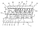
最初に、図1Aに示す半導体素子の実装工程について説明する。
まず、回路基板1の表面には、導電性を有する基板電極2(接続端子)と、図示を省略する配線パターンとが形成される。回路基板1は、例えば、BTレジン樹脂(登録商標)などの樹脂材料から製造されており、その厚さを例えば0.35mmとする。基板電極2には、例えば、金や銅が用いられ、フォトリソグラフィー法により形成される。基板電極2は、例えば、100μmの間隔で400個程度形成される。
Hereinafter, preferred embodiments of the present invention will be described with reference to the drawings. In the drawings, similar components are given the same reference numerals.
(First embodiment)
First, the mounting process of the semiconductor element shown in FIG. 1A will be described.
First, a conductive substrate electrode 2 (connection terminal) and a wiring pattern (not shown) are formed on the surface of the circuit board 1. The circuit board 1 is manufactured from, for example, a resin material such as BT resin resin (registered trademark), and has a thickness of, for example, 0.35 mm. For example, gold or copper is used for the
次に、回路基板1の所定位置に第1の半導体素子10を位置合わせして実装する。
第1の半導体素子10には、半導体回路が形成されており、電極の無い一方の面を下向きにして、ダイボンディング材13によって回路基板1に接着されている。なお、第1の半導体素子10は、パッケージ型の半導体素子であっても良い。
Next, the
The
さらに、基板11の他方の面11Aには、第1の電極パッド14と、第2の電極パッド15と、第3の電極パッド16がそれぞれ間隔をおいて複数配設されている。これら電極パッド14〜16は、第1の半導体素子10の半導体回路に電気的に接続されている。例えば、Alや、Cuなどから製造されている。電極パッド14〜16は、例えば、電解めっき、又は無電解めっきにより、同じ膜厚に形成される。
Further, a plurality of
図1Aの側面図及び図2Aの平面図に示すように、第1の電極パッド14は、第1の半導体素子10の他方の面11Aに所定の間隔、例えば50μmのピッチで複数配列され、フリップチップ接続用のバンプを形成するために用いられる。
図1Aに示すように、第1の電極パッド14の上には、導電性材料であるハンダバンプ17が形成される。ハンダバンプ17のハンダ材料には、SnAg系のSn−3.5Agが用いられる。このようなハンダバンプ17は、例えば、第1の電極パッド14の上にスクリーン印刷で塗布したハンダペーストをリフロー工程で溶融させることで形成される。また、第1の電極パッド14の上にフラックを介してハンダボールを接着し、リフロー工程によりハンダボールを溶融させることで形成しても良い。なお、ハンダ材料は、SnAg系に限定されない。また、ハンダバンプ17の代わりに、金バンプを用いても良い。
As shown in the side view of FIG. 1A and the plan view of FIG. 2A, a plurality of
As shown in FIG. 1A, a
図2Aに示すように、第2の電極パッド15と第3の電極パッド16は、基板11の外周部分に所定の間隔で複数配列され、共に、回路基板1とのワイヤボンディング用に用いられる。
第2の電極パッド15は、周囲に第1の電極パッド14が形成されている領域R1に、複数の第1の電極パッド14の間に1つずつ形成される。図3の拡大図に示すように、第2の電極パッド15は、第1の電極パッド14が円形の場合には、四角形の四隅が円弧状に切り取られた、略X字の平面形状を有する。この領域R1における第2の電極パッド15の形状は、第1の電極パッド14を避け、かつボンディング用のワイヤと十分な接触面積が得られる形状及び大きさである。
As shown in FIG. 2A, a plurality of
The
また、第3の電極パッド16は、基板11上で、周囲に第1の電極パッド14が形成されていない領域R2に円形に形成される。
The
次に、図1B及び図2Bに示すように、第1の半導体素子10上の第2の電極パッド15と、回路基板1上の基板電極2とを、ワイヤ18で電気的に接続する。同様に、第3の電極パッド16と、回路基板1上の基板電極2とを、ワイヤ18で電気的に接続する。ワイヤ18には、導電性材料で9ナインなどの高純度の金などが用いられる。ワイヤ18の直径は、例えば20μmである。
Next, as shown in FIGS. 1B and 2B, the
ここで、図3に示すように、ワイヤ18は、第2の電極パッド15に電気的に接続されると共に、第2の電極パッド15よりも外側に配置されている2つの第1の電極パッド14及びその上の2つのハンダバンプ17の間の上方を通って、基板電極2に引き出される。
Here, as shown in FIG. 3, the
続いて、図1Cの構造を得るまでの工程について説明する。
第1の半導体素子10の上に実装される第2の半導体素子20には、半導体回路が形成されている。第2の半導体素子20のサイズは、第1の半導体素子10より大きいものが実装される。なお、第2の半導体素子20は、パッケージ型の半導体素子であっても良い。
Next, steps required until a structure shown in FIG. 1C is obtained will be described.
A semiconductor circuit is formed on the
第2の半導体素子20の一方の面21Aは、下向きに配置され、複数の電極パッド24が配設されている。電極パッド24は、第2の半導体素子20の半導体回路に電気的に接続されており、例えば、Alや、Cuなどから製造されている。さらに、電極パッド24上には、フリップチップ接続用の接続端子26が柱状に形成されている。電極パッド24及び接続端子26の配置間隔は、ワイヤ18の径より大きい。なお、接続端子26は、断面で示されている。
One
接続端子26は、Cu、Au、Ni、W等、導電性を有する材料から製造される。接続
端子26をCu、Au、Niで製造するときは、接続端子26は、電解めっきにより形成される。その形成方法を次に説明する。
The
最初に、電解めっきの電極となるシード層(不図示)を電極パッド24及び第2の半導体素子20の表面に形成する。さらに、図4Aに示すように、第2の半導体素子20の一方の面の上にフォトレジストを塗布し、硬化させた後に露光及び現像することにより、電極パッド24上に開口部27Aを有するレジストパターン27を形成する。
First, a seed layer (not shown) to be an electrode for electrolytic plating is formed on the
この後、図4Bに示すように、電解めっきにより、レジストパターン27の開口部27A内に接続端子26を成長させる。接続端子26を成長させた後、レジストパターン27を有機溶剤又はアッシングにより除去する。さらに、第2の半導体素子20上の不図示のシード層を酸性溶液などを用いてエッチングして除去する。なお、接続端子26は、無電解めっきで形成しても良い。
Thereafter, as shown in FIG. 4B, the
また、接続端子26をWで製造するときは、CVD(Chemical Vapor Deposition)法、又はスパッタ法を用いて電極パッド24上に形成する。
なお、接続端子26は、低弾性で導電性を有する材料から製造されていれば良く、例えば、樹脂材料に金属フィラーを混合させた導電性接着剤や、樹脂材料にカーボンナノチューブを分散させた複合材であっても良い。
Further, when the
The
ここで、図1Cに示すように、接続端子26の高さは、ワイヤ18のループ高さH1以上になっており、例えば50μmである。なお、ループ高さH1は、第1の半導体素子10上の第2、第3の電極パッド14,15の上面から、ワイヤ18のループの最も高い部分までの距離である。
また、回路基板1の表面に平行な断面において、接続端子26は円形になっている。なお、回路基板1の表面に平行な断面における接続端子26の断面形状は、楕円や、角形、その他の多角形であっても良い。また、接続端子26の外形は、円錐や角錐、円錐台、角錐台でも良い。
Here, as shown in FIG. 1C, the height of the
Further, the
続いて、図4Cに示すように、接続端子26の外側面に、絶縁樹脂28を塗布する。絶縁樹脂28としては、シリコーンエラストマように伸縮性の高い樹脂が用いられる。絶縁樹脂28の塗布方法としては、例えば、スピンコート法が用いられる。なお、ここまでの工程は、半導体回路が形成された半導体ウェハ上で実施され、接続端子26及び絶縁樹脂28の形成を行った後、ダイシングにより第2の半導体素子20毎に分割される。
Subsequently, as shown in FIG. 4C, an insulating
次に、接続端子26の露出している端面26Aにフラックスを塗布し、接続端子26と第1の半導体素子10上のハンダバンプ17に位置合わせしてから、図1Cに示すように、第2の半導体素子20をダウンフェイスで対向させ、第1の半導体素子10にフリップチップ実装する。第2の半導体素子20は、第1の半導体素子10より大きいので、第2の電極パッド15及び第3の電極パッド16の上方が第2の半導体素子20で覆われる。このとき、接続端子26の間に、第2の電極パッド15に接続されたワイヤ18を通らせる。
Next, a flux is applied to the exposed
フリップチップ実装時には、例えば、約20Nの荷重を1.5秒かけて第2の半導体素子20を第1の半導体素子10に仮接着し、その後にリフロー炉で最大温度250℃まで加熱してハンダバンプ17を溶融させる。これにより、接続端子26とハンダバンプ17とが接合され、第1の半導体素子10の電極パッド14と第2の半導体素子20の電極パッド24が電気的に接続される。また、この際、絶縁樹脂28の一部が溶融して流れ、接続端子26の下側に配置されているハンダバンプ17の表面を覆う。
At the time of flip-chip mounting, for example, the
ここで、背高の接続端子26の存在によって、第1の半導体素子10の第2の電極パッド15に接続されたワイヤ18は、第2の半導体素子20に接触することなく、隣り合う2つの接続端子26の間から回路基板1に引き出される。さらに、接続端子26の外側面に絶縁樹脂28が塗布されているので、ワイヤ18と接続端子26が短絡することはない。同様に、第1の半導体素子10の第3の電極パッド16に接続されたワイヤ18は、第2の半導体素子20に接触することなく、回路基板1に引き出される。
Here, due to the presence of the
この後、フラックスを洗浄してから、第1の半導体素子10と、第2の半導体素子20の間の隙間にアンダーフィル材29を充填し、加熱硬化させる。この結果、接続端子26及びワイヤ18の一部が樹脂封止される。
Thereafter, after the flux is washed, an
これにより、第1、第2の半導体素子10,20が順に回路基板1上に実装されると共に、第1の半導体素子10の第2、第3の電極パッド15,16がワイヤ18で基板電極2に電気的に接続され、半導体装置31が完成する。なお、半導体装置31の回路基板1上には、図示を省略する他の部品を実装しても良い。
As a result, the first and
以上、説明したように、この半導体装置31では、第2の半導体素子20に背高の導電性部材である接続端子26を設け、第1の半導体素子10と第2の半導体素子20の電極パッド14,24間の距離H0を、ワイヤ18のループ高さH1より高くした。これにより、第1の半導体素子10より第2の半導体素子20が大きい場合でも、第1の半導体素子10と回路基板1とをワイヤ18で直接、電気的に接続することが可能になる。しかも、従来のように、2つの半導体装置の間にインターポーザを介挿させる必要がなくなるので、製造工程が簡略化される。また、装置構成が簡単になるので、半導体装置を従来に比べて小型化できる。
As described above, in the
また、接続端子26の間からワイヤ18を通して基板電極2に電気的に接続するようにしたので、第1の半導体素子10を小型化できる。ここで、接続端子26の外表面に絶縁樹脂28を設けてあるので、ワイヤ18と接続端子26とが短絡することはない。したがって、第1の半導体素子10に第1の電極パッド14と第2の電極パッド15をより狭い間隔で配置できる。
Further, since the connection to the
なお、図5に示すように、第2の半導体素子20は、必ずしも第1の半導体素子10より大きくなくて良い。この変形例では、第2の半導体素子20は、第1の半導体素子10より小さく、かつ、一つの辺に沿った部分のみが第2の電極パッド15の上を覆っている。
このように、この半導体装置31によれば、第2の半導体素子20が第1の半導体素子10以下のサイズであっても、第2の半導体素子20が第1の半導体素子10に重なる部分に、第2の電極パッド15と、接続端子26を設けることで、インターポーザを介挿させることなく、第1の半導体素子10と回路基板1とをワイヤ18で電気的に接続できる。
As shown in FIG. 5, the
As described above, according to the
なお、第2の半導体素子20は、2つの辺に沿った部分、又は3つの辺の沿った部分が第2の電極パッド15の上を覆っても良い。
また、半導体装置31は、3つ以上の半導体素子を積層しても良い。さらに、接続端子26を第1の半導体素子10に設け、ハンダバンプ17を第2の半導体素子20に設けても良い。
The
The
(第2の実施の形態)
最初に、図6Aに示す半導体素子の実装工程について説明する。
回路基板1上には、第1の半導体素子10が実装される。第1の半導体素子10は、第
1、第2、第3の電極パッド14〜16が複数形成されており、第1の電極パッド14の上には、第1の接続端子43が形成されている。
(Second Embodiment)
First, the mounting process of the semiconductor element shown in FIG. 6A will be described.
A
第1の接続端子43は、Cu、Au、Ni、W等の金属材料から製造される。第1の接続端子43は、第1の実施の形態の接続端子26の製造方法と同様な工程により、電解めっき又は無電解めっき、或いはCVD法やスパッタ法により形成される。第1の接続端子43の配置間隔は、ワイヤ18の径より大きい。また、第1の接続端子43の高さは、ワイヤ18のループ高さH1より低い。
The
第1の半導体素子10を回路基板1にダイボンディング材13で接着した後に、第2の電極パッド15及び第3の電極パッド16と回路基板1の基板電極2がワイヤ18で電気的に接続される。第2の電極パッド15に接合されるワイヤ18は、第1の接続端子43の間を通って、回路基板1に引き出される。
After the
続いて、図6Bに示すように、第1の半導体素子10の上に、第2の半導体素子20が実装される。第2の半導体素子20は、第1の半導体素子10の外周寄りの第2の電極パッド15、第3の電極パッド16の少なくとも一部の上を覆う。第2の半導体素子20は、電極パッド24に第2の接続端子44が接続されており、第2の接続端子44の下には導電性部材であるハンダバンプ45が設けられ、ハンダバンプ45を介して、第1の接続端子43と第2の接続端子44が接続される。
Subsequently, as shown in FIG. 6B, the
ここで、図7A及び図7Bを参照して、第2の半導体素子20の第2の接続端子44及びハンダバンプ45の製造方法について説明する。
図7Aに示すように、第2の接続端子44は、Cu、Au、Ni、W等の金属材料を用いて、第1の接続端子43と同様に、電解めっき又は無電解めっき、或いはCVD法やスパッタ法により形成される。第2の接続端子44及びハンダバンプ45の配置間隔は、ワイヤ18の径より大きい。
Here, with reference to FIGS. 7A and 7B, a method for manufacturing the
As shown in FIG. 7A, the
続いて、第2の接続端子44の上に、ハンダバンプ45を形成する。ハンダバンプ45のハンダ材料には、例えば、SnAg系のSn−3.5Agが用いられる。ハンダバンプ45は、第1の実施の形態のハンダバンプ17と同様の方法で形成される。また、ハンダバンプ45の代わりに、Au、In、導電性接着剤等、塑性変形し易く導電性を有する材料を用いても良い。
Subsequently, a
続いて、第2の半導体素子20の一方の面21Aとその上の電極パッド24、第2の接続端子44、ハンダバンプ45の表面を絶縁樹脂28でコーティングする。絶縁樹脂28は、伸縮性の高い樹脂が用いられる。絶縁樹脂28として、パラキシリレン樹脂を用いるときは、第2の半導体素子20を真空中で加熱し、パラキシリレン樹脂を第2の接続端子44及びハンダバンプ45の表面に蒸着する
なお、絶縁樹脂に、シリコーンエラストマや、ポリオレフィン樹脂、ポリイミド樹脂を用いるときは、スピンコート法で塗布する。
Subsequently, one
この後、図7Bに示すように、ハンダバンプ45の上端部分とその表面の絶縁樹脂28を、例えばダイヤモンドバイト46で切削し、ハンダバンプ45の表面を露出させる。
Thereafter, as shown in FIG. 7B, the upper end portion of the
そして、図6Bに示すように、ハンダバンプ45の露出した端面45Aを第1の半導体素子10の第1の接続端子43の上端に位置合わせして当接させる。この際、第2の接続端子44の間にワイヤ18が通される。
続いて、例えば、約20Nの荷重を1.5秒かけて第2の半導体素子20を第1の半導体素子10に仮接着し、その後にリフロー炉で最大温度250℃まで加熱してハンダバン
プ45を溶融させる。これにより、ハンダバンプ45と第1の接続端子43が接合され、第1の半導体素子10の第1の電極パッド14と第2の半導体素子20の電極パッド24とが電気的に接続される。
Then, as shown in FIG. 6B, the exposed
Subsequently, for example, the
ここで、この半導体装置41では、第1の半導体素子10と第2の半導体装置の電極パッド14,24間の距離H0が、ワイヤ18のループ高さH1より高くなるように、接続端子43,44及びハンダバンプ45が形成されており、その高さは例えば50μmである。したがって、ワイヤ18が第2の半導体素子20に接触することはない。さらに、第1の半導体素子10の第2の電極パッド15に接合されたワイヤ18は、ハンダバンプ45の上側を通って隣り合う2つの接続端子44の間から、回路基板1に引き出される。第2の接続端子44及びハンダバンプ45の外側面には絶縁樹脂28が塗布されているので、ワイヤ18と短絡することはない。
Here, in the
なお、ワイヤ18がハンダバンプ45の上側を通って回路基板1に引き出されるため、下側の第1の接続端子43の外側面に絶縁樹脂28を塗布する必要はない。しかしながら、第1の接続端子43の外側面に絶縁樹脂28を塗布しても良い。
Since the
この後、第1の半導体素子10と、第2の半導体素子20の間の隙間にアンダーフィル材29を充填し、加熱硬化させる。これにより、接続端子43,44及びハンダバンプ45と、ワイヤ18の一部が樹脂封止され、半導体装置41が完成する。なお、半導体装置41には、図示を省略する他の部品を実装しても良い。
Thereafter, the
以上、説明したように、この半導体装置41では、第1、第2の半導体素子10,20のそれぞれに接続端子43,44を設け、2つの半導体素子10,20の電極パッド14,24間の距離H0をワイヤ18のループ高さH1より高くした。これにより、2つの半導体素子10,20の間にインターポーザを介挿させる必要がなくなる。
さらに、第1、第2の半導体素子10,20のそれぞれに接続端子43,44を設けたので、1つ1つの接続端子43,44の長さを小さくでき、製造が容易になる。
さらに、接続端子43,44の接合時にハンダバンプ45を加圧することで塑性変形させて、接続端子43,44より外側に突出する突出部を形成したので、ワイヤ18が通る隙間を減少させることができる。これにより、ワイヤ18のループの変形や、ワイヤ18の傾倒が抑制される。その他の効果は、第1の実施の形態と同じである。
As described above, in the
Furthermore, since the
Further, since the
ここで、この実施の形態の変形例について説明する。
図8Aに示すように、ハンダバンプ45を第1の半導体素子10の第1の接続端子43に接合する際に、加熱しながら荷重をさらにかけて、ハンダバンプ45をつぶす。これにより、ハンダバンプ45が側方に突出する。
図8Bに示すように、この変形例では、ハンダバンプ45をさらにつぶして、側方に突出させたので、突出部となるハンダバンプ45の間の距離がさらに短くなり、ワイヤ18の外径より小さくなる。これにより、ワイヤ18のループの変形や、ワイヤ18の傾倒をさらに抑制できる。
Here, a modified example of this embodiment will be described.
As shown in FIG. 8A, when the
As shown in FIG. 8B, in this modification, since the
なお、図6及び図8Aにおいて、第1、第2の接続端子43,44の長さは、略等しく、ハンダバンプ45は、2つの半導体素子10,20の間の距離の中間位置に配置されている。しかしながら、第1の接続端子43と第2の接続端子44の長さを異ならせても良い。
また、第2の実施の形態における絶縁樹脂28のコーティング方法を用いて、第1の実施の形態の絶縁樹脂28を形成しても良い。
6 and 8A, the lengths of the first and
Further, the insulating
(第3の実施の形態)
図9に示すように、半導体装置51は、回路基板1上に第1の半導体素子10が実装され、第2の電極パッド15及び第3の電極パッド16と回路基板1の基板電極2とがワイヤ18で電気的に接続されている。さらに、第1の半導体素子10の上には、第2の半導体素子20が実装されている。第2の半導体素子20は、第1の半導体素子10の第2の電極パッド15、第3の電極パッド16の少なくとも一部の上を覆う外形を有する。
(Third embodiment)
As shown in FIG. 9, in the
ここで、第1の半導体素子10の第1の電極パッド14の上には、ハンダバンプ17が形成されている。ハンダバンプ17は、例えばSnAg系のSn−3.5Agから形成される。さらに、ハンダバンプ17の表面は、絶縁樹脂28でコーティングされる。絶縁樹脂28のコーティング方法は、前記のいずれかの実施の形態と同様である。
Here, solder bumps 17 are formed on the
また、第2の半導体素子20の電極パッド24には、接続端子52が接続されている。接続端子52は、例えば、AuやCu等の導電性材料から製造される。
A
ここで、図10を参照して、接続端子52の製造方法について説明する。
まず、基板21に形成した電極パッド24の上に、第1のバンプ53を形成する。続いて、第1のバンプ53の上に第2のバンプ54を重ねて形成する。これにより、接続端子52が形成される。これらバンプ53,54は、ワイヤボンディング技術を用いてボール状に形成される。
さらに、各接続端子52,54を絶縁樹脂28でコーティングする。絶縁樹脂28のコーティング方法は、前記のいずれかの実施の形態と同様である。なお、接続端子52の配置間隔は、絶縁樹脂28を塗布した後でも、ワイヤ18を通すのに十分な大きさである。
Here, with reference to FIG. 10, the manufacturing method of the
First, the
Further, the
第2の半導体素子20を第1の半導体素子10の上に実装するときは、第1の半導体素子10のハンダバンプ17の上に、第2の半導体素子20の接続端子52を位置決めして載置する。このとき、ワイヤ18が接続端子52の間の隙間に通される。
When the
ここで、第2のバンプ54の先端に形成された突起54Aが、ハンダバンプ17に刺さり、第2の半導体素子20が第1の半導体素子10に仮固定される。続いて、例えば、約20Nの荷重を1.5秒かけてから、リフロー炉で最大温度250℃まで加熱してハンダバンプ17を溶融させる。これにより、ハンダバンプ17と接続端子52とが接合され、第1の半導体素子10の第1の電極パッド14と第2の半導体素子20の電極パッド24とが電気的に接続される。
Here, the
ここで、第1の半導体素子10と第2の半導体装置の電極パッド14,24間の距離H0が、ワイヤ18のループ高さH1より高くなるように、接続端子52が形成されている。したがって、ワイヤ18が第2の半導体素子20に接触することはない。第2の電極パッド15に接続されたワイヤ18は、隣り合う2つの接続端子52の間から、回路基板1に引き出される。接続端子52及びハンダバンプ17の外側面には絶縁樹脂28が塗布されているので、ワイヤ18と接続端子52及びハンダバンプ17が短絡することはない。なお、ハンダバンプ17の外側面には、絶縁樹脂28を塗布しなくても良い。
Here, the
この後、第1の半導体素子10と、第2の半導体素子20の間の隙間にアンダーフィル材29を充填し、加熱硬化させる。これにより、ハンダバンプ17及び接続端子52と、ワイヤ18の一部が樹脂封止され半導体装置51が完成する。なお、半導体装置51には、図示を省略する他の部品を実装しても良い。
Thereafter, the
以上、説明したように、この半導体装置51では、バンプ53,54を重ね合わせて接続端子52を形成したので、接続端子52を容易に製造できる。その他の効果は、第1、第2の実施の形態と同じである。
As described above, in the
ここで挙げた全ての例及び条件的表現は、発明者が技術促進に貢献した発明及び概念を読者が理解するのを助けるためのものであり、ここで具体的に挙げたそのような例及び条件に限定することなく解釈するものであり、また、明細書におけるそのような例の編成は本発明の優劣を示すこととは関係ない。本発明の実施形態を詳細に説明したが、本発明の精神及び範囲から逸脱することなく、それに対して種々の変更、置換及び変形を施すことができる。 All examples and conditional expressions given here are intended to help the reader understand the inventions and concepts that have contributed to the promotion of technology, and such examples and It is to be construed without being limited to the conditions, and the organization of such examples in the specification is not related to showing the superiority or inferiority of the present invention. While embodiments of the present invention have been described in detail, various changes, substitutions and variations can be made thereto without departing from the spirit and scope of the present invention.
以下に、前記の実施の形態の特徴を付記する。
(付記1)基板と、前記基板にフェイスアップで実装され、第1の電極パッドと第2の電極パッドが設けられた第1の半導体素子と、前記第1の電極パッド及び第2の電極パッドの上方を覆い、かつ第1の半導体素子に前記第1の電極パッドを介してフェイスダウンで実装される第2の半導体素子と、前記第2の電極パッドと前記基板に設けられた基板電極とを電気的に接続する導電性のワイヤと、前記第1の半導体素子の前記第1の電極パッドと前記第2の半導体素子の電極との間に接続され、前記第1、第2の半導体素子の間の距離を、前記第2の電極パッドから前記ワイヤのループの上端までの高さより大きくする高さを有する接続端子と、を含む半導体装置。
(付記2) 前記ワイヤは、前記接続端子の間を通って前記基板に引き出され、前記接続端子に電気的に接続されている付記1に記載の半導体装置。
(付記3) 前記接続端子の表面に絶縁樹脂がコーティングされている付記2に記載の半導体装置。
(付記4) 前記接続端子は、前記第1の半導体素子の前記第1の電極パッド上に形成された第1の接続端子と、前記第2の半導体素子の前記電極上に形成された第2の接続端子とを含む付記1乃至請求3のいずれか一項に記載の半導体装置。
(付記5) 前記第1の接続端子と第2の接続端子の間に形成され、かつ前記第1、第2の接続端子より側方に突出する導電性部材を有し、前記導電性部材の表面は前記絶縁樹脂でコーティングされている付記4に記載の半導体装置。
(付記6) 隣り合う前記導電性部材の間の距離は、前記ワイヤの径以下である付記5に記載の半導体装置。
(付記7) 前記接続端子は、バンプを重ねて形成されている付記1乃至付記3のいずれか一項に記載の半導体装置。
(付記8) 前記第1の半導体素子において、前記第2の電極パッドは前記第1の電極パッドより内側に形成されている付記1乃至付記7のいずれか一項に記載の半導体装置。
(付記9) 第1の電極パッドと第2の電極パッドを有する第1の半導体素子のうち、前記第1の電極パッド上に第1の接続端子を形成する工程と、基板に前記第1の半導体素子をフェイスアップで接着する工程と、前記第1の半導体素子上の前記第2の電極パッドと、前記基板の基板電極とを導電性のワイヤで接続する工程と、第2の半導体素子の電極上に第2の接続端子を形成する工程と、前記第2の半導体素子を前記第1の半導体素子にフェイスダウンで対向させ、前記第1の接続端子の上に導電性部材を介して前記第2の接続端子を載置し、前記第2の接続端子の間に前記ワイヤを通す工程と、前記導電性材料を潰しつつ、前記第1の接続端子を前記第2の接続端子に接続させる工程と、を含む半導体装置の製造方法。
(付記10) 前記導電性材料を側方に突出させ、隣り合う前記導電性材料の間の距離を前記ワイヤの径以下にする工程を含む付記9に記載の半導体装置の製造方法。
(付記11) 前記導電性材料及び前記第2の接続端子に絶縁樹脂を蒸着した後、前記導電性材料及び前記絶縁樹脂の一部をカットして前記導電性材料の端面を露出させる工程を含む付記9に記載の半導体装置の製造方法。
The features of the above embodiment will be added below.
(Appendix 1) A substrate, a first semiconductor element mounted face-up on the substrate and provided with a first electrode pad and a second electrode pad, and the first electrode pad and the second electrode pad A second semiconductor element that is mounted face-down on the first semiconductor element via the first electrode pad, a substrate electrode provided on the substrate, the second electrode pad, A conductive wire that electrically connects the first and second semiconductor elements, and a conductive wire that is connected between the first electrode pad of the first semiconductor element and the electrode of the second semiconductor element. A connection terminal having a height that makes the distance between the second electrode pad and the upper end of the loop of the wire larger than the distance between the connection terminals.
(Additional remark 2) The said wire is a semiconductor device of Additional remark 1 currently pulled out to the said board | substrate through between the said connection terminals, and being electrically connected to the said connection terminal.
(Supplementary note 3) The semiconductor device according to
(Supplementary Note 4) The connection terminal includes a first connection terminal formed on the first electrode pad of the first semiconductor element, and a second connection terminal formed on the electrode of the second semiconductor element. 4. The semiconductor device according to claim 1, further comprising: a connection terminal.
(Supplementary Note 5) A conductive member formed between the first connection terminal and the second connection terminal and projecting laterally from the first and second connection terminals. The semiconductor device according to appendix 4, wherein a surface is coated with the insulating resin.
(Additional remark 6) The distance between the said adjacent electroconductive members is a semiconductor device of Additional remark 5 which is below the diameter of the said wire.
(Supplementary note 7) The semiconductor device according to any one of supplementary notes 1 to 3, wherein the connection terminal is formed by overlapping bumps.
(Supplementary note 8) The semiconductor device according to any one of supplementary notes 1 to 7, wherein, in the first semiconductor element, the second electrode pad is formed inside the first electrode pad.
(Supplementary Note 9) Of a first semiconductor element having a first electrode pad and a second electrode pad, a step of forming a first connection terminal on the first electrode pad, and a step of forming the first connection terminal on a substrate Bonding a semiconductor element face up; connecting the second electrode pad on the first semiconductor element to a substrate electrode of the substrate with a conductive wire; and Forming a second connection terminal on the electrode; and facing the second semiconductor element to the first semiconductor element face-down, and passing the conductive member on the first connection terminal via a conductive member. Placing the second connection terminal and passing the wire between the second connection terminals, and connecting the first connection terminal to the second connection terminal while crushing the conductive material A method of manufacturing a semiconductor device.
(Additional remark 10) The manufacturing method of the semiconductor device of Additional remark 9 including the process of making the said electroconductive material protrude to the side, and making the distance between the said adjacent electroconductive materials below the diameter of the said wire.
(Additional remark 11) After vapor-depositing insulating resin on the said electroconductive material and the said 2nd connection terminal, the process of cutting a part of the said electroconductive material and the said insulating resin, and exposing the end surface of the said electroconductive material is included. A method for manufacturing a semiconductor device according to appendix 9.
1 回路基板
2 基板電極(接続端子)
10 第1の半導体素子
14 第1の電極パッド(電極)
15 第2の電極パッド
16 第3の電極パッド(第2の電極パッド)
17 ハンダバンプ
18 ワイヤ
20 第2の半導体素子
24 電極パッド(電極)
26,52 接続端子
28 絶縁樹脂
31,41,51 半導体装置
43 第1の接続端子
44 第2の接続端子
45 ハンダバンプ(導電性部材)
53 第1の端子
54 第2の端子
H0 半導体素子間の距離
H1 ループの高さ
1
10
15
17
26, 52
53
Claims (5)
前記基板にフェイスアップで実装され、第1の電極パッドと第2の電極パッドが設けられた第1の半導体素子と、
前記第1の電極パッド及び第2の電極パッドの上方を覆い、かつ第1の半導体素子に前記第1の電極パッドを介してフェイスダウンで実装される第2の半導体素子と、
前記第2の電極パッドと前記基板に設けられた基板電極とを電気的に接続する導電性のワイヤと、
前記第1の半導体素子の前記第1の電極パッドと前記第2の半導体素子の電極との間に接続され、前記第1、第2の半導体素子の間の距離を、前記第2の電極パッドから前記ワイヤのループの上端までの高さより大きくする高さを有する接続端子と、
を含み、
前記ワイヤは、前記第2の電極パッドの外側に配置された複数の前記接続端子の間を通り、平面視で前記ワイヤが延在する方向に垂直な方向において複数の前記接続端子の間より広い幅を有する前記第2の電極パッドと前記基板電極とを電気的に接続していることを特徴とする半導体装置。 A substrate,
A first semiconductor element mounted face up on the substrate and provided with a first electrode pad and a second electrode pad;
A second semiconductor element that covers the first electrode pad and the second electrode pad and is mounted face-down on the first semiconductor element via the first electrode pad;
A conductive wire that electrically connects the second electrode pad and a substrate electrode provided on the substrate;
The second electrode pad is connected between the first electrode pad of the first semiconductor element and the electrode of the second semiconductor element, and the distance between the first and second semiconductor elements is defined as the second electrode pad. A connection terminal having a height greater than the height from the wire to the upper end of the loop of the wire;
Including
The wire passes between the plurality of connection terminals arranged outside the second electrode pad and is wider than the space between the plurality of connection terminals in a direction perpendicular to the direction in which the wire extends in a plan view. A semiconductor device, wherein the second electrode pad having a width and the substrate electrode are electrically connected.
前記第2の電極パッドと、前記基板に設けられた基板電極とを導電性のワイヤで接続する工程と、
第2の半導体素子を前記第1の半導体素子にフェイスダウンで対向させ、前記第1の電極パッドと前記第2の半導体素子の電極とを接続端子を介して、前記第1、第2の半導体素子の間の距離を、前記第2の電極パッドから前記ワイヤのループの上端までの高さより大きくするように接続し、前記ワイヤを前記第2の電極パッドの外側に配置される複数の前記接続端子の間に通す工程と、
を有し、
前記ワイヤを接続する工程は、平面視で前記ワイヤが延在する方向に垂直な方向において複数の前記接続端子の間より広い幅を有する前記第2の電極パッドと前記基板電極とを電気的に接続することを特徴とする半導体装置の製造方法。 Bonding a first semiconductor element provided with a first electrode pad to the substrate and a second electrode pad disposed inside the first electrode pad face up;
Connecting the second electrode pad and a substrate electrode provided on the substrate with a conductive wire;
A second semiconductor element is made to face the first semiconductor element face down, and the first and second semiconductors are connected via a connection terminal between the first electrode pad and the electrode of the second semiconductor element. A plurality of the connections arranged such that a distance between the elements is larger than a height from the second electrode pad to an upper end of a loop of the wire, and the wire is disposed outside the second electrode pad; Passing between terminals;
Have
The step of connecting the wires electrically connects the second electrode pad and the substrate electrode having a wider width between the plurality of connection terminals in a direction perpendicular to the direction in which the wires extend in a plan view. A method for manufacturing a semiconductor device, comprising: connecting.
Priority Applications (1)
| Application Number | Priority Date | Filing Date | Title |
|---|---|---|---|
| JP2010076592A JP5696367B2 (en) | 2010-03-30 | 2010-03-30 | Semiconductor device and manufacturing method thereof |
Applications Claiming Priority (1)
| Application Number | Priority Date | Filing Date | Title |
|---|---|---|---|
| JP2010076592A JP5696367B2 (en) | 2010-03-30 | 2010-03-30 | Semiconductor device and manufacturing method thereof |
Publications (2)
| Publication Number | Publication Date |
|---|---|
| JP2011210913A JP2011210913A (en) | 2011-10-20 |
| JP5696367B2 true JP5696367B2 (en) | 2015-04-08 |
Family
ID=44941665
Family Applications (1)
| Application Number | Title | Priority Date | Filing Date |
|---|---|---|---|
| JP2010076592A Expired - Fee Related JP5696367B2 (en) | 2010-03-30 | 2010-03-30 | Semiconductor device and manufacturing method thereof |
Country Status (1)
| Country | Link |
|---|---|
| JP (1) | JP5696367B2 (en) |
Family Cites Families (7)
| Publication number | Priority date | Publication date | Assignee | Title |
|---|---|---|---|---|
| JP2645235B2 (en) * | 1996-01-26 | 1997-08-25 | 株式会社東芝 | Wire bonding method |
| JPH1056041A (en) * | 1996-06-04 | 1998-02-24 | Citizen Watch Co Ltd | Structure and method for mounting semiconductor device |
| JP3286182B2 (en) * | 1996-09-19 | 2002-05-27 | 株式会社東芝 | Semiconductor device and manufacturing method thereof |
| KR100541393B1 (en) * | 2003-04-26 | 2006-01-10 | 삼성전자주식회사 | Multi-chip BGA package |
| JP2005150441A (en) * | 2003-11-17 | 2005-06-09 | Matsushita Electric Ind Co Ltd | Chip laminated semiconductor device and its manufacturing method |
| JP5217043B2 (en) * | 2007-07-11 | 2013-06-19 | ルネサスエレクトロニクス株式会社 | Manufacturing method of semiconductor device |
| JP5553960B2 (en) * | 2007-10-25 | 2014-07-23 | スパンション エルエルシー | Semiconductor device and manufacturing method thereof |
-
2010
- 2010-03-30 JP JP2010076592A patent/JP5696367B2/en not_active Expired - Fee Related
Also Published As
| Publication number | Publication date |
|---|---|
| JP2011210913A (en) | 2011-10-20 |
Similar Documents
| Publication | Publication Date | Title |
|---|---|---|
| JP4618260B2 (en) | Conductor pattern forming method, semiconductor device manufacturing method, and semiconductor device | |
| US9935072B2 (en) | Semiconductor package and method for manufacturing the same | |
| TWI541916B (en) | Semiconductor device and method of forming flipchip interconnect structure | |
| US20130113099A1 (en) | Package carrier, package carrier manufacturing method, package structure for semiconductor device and manufacturing method thereof | |
| JP2017152646A (en) | Electronic component, electronic device and electronic apparatus | |
| TWI480989B (en) | Semiconductor package and fabrication method thereof | |
| US8772922B2 (en) | Chip structure having redistribution layer | |
| WO2015198839A1 (en) | Semiconductor device and manufacturing method therefor | |
| JP2008235365A (en) | Wiring board, packaging structure of electronic component, and semiconductor device | |
| JP2012015142A (en) | Semiconductor package and manufacturing method of the same | |
| US10276465B2 (en) | Semiconductor package assembly | |
| JP2012064991A (en) | Flip-chip bonded package | |
| JP5973470B2 (en) | Semiconductor device | |
| JP6495130B2 (en) | Semiconductor device and manufacturing method thereof | |
| JP6544354B2 (en) | Semiconductor device manufacturing method | |
| JP2018037520A (en) | Semiconductor device, electronic device, method for manufacturing semiconductor device, and method for manufacturing electronic device | |
| JP5696367B2 (en) | Semiconductor device and manufacturing method thereof | |
| JP2002343930A (en) | Semiconductor device | |
| US9666530B1 (en) | Semiconductor device | |
| JP5151584B2 (en) | Semiconductor device and manufacturing method of semiconductor device | |
| TWI375307B (en) | Flip chip package structure and method for manufacturing the same | |
| JP4728079B2 (en) | Semiconductor device substrate and semiconductor device | |
| TWI689067B (en) | Electronic package and method for fabricating the same | |
| JP2012023409A (en) | Circuit device and method for manufacturing thereof | |
| JP2017183571A (en) | Manufacturing method of semiconductor device |
Legal Events
| Date | Code | Title | Description |
|---|---|---|---|
| A621 | Written request for application examination |
Free format text: JAPANESE INTERMEDIATE CODE: A621 Effective date: 20130206 |
|
| A977 | Report on retrieval |
Free format text: JAPANESE INTERMEDIATE CODE: A971007 Effective date: 20130924 |
|
| A131 | Notification of reasons for refusal |
Free format text: JAPANESE INTERMEDIATE CODE: A131 Effective date: 20131001 |
|
| A521 | Written amendment |
Free format text: JAPANESE INTERMEDIATE CODE: A523 Effective date: 20131202 |
|
| A131 | Notification of reasons for refusal |
Free format text: JAPANESE INTERMEDIATE CODE: A131 Effective date: 20140513 |
|
| A521 | Written amendment |
Free format text: JAPANESE INTERMEDIATE CODE: A523 Effective date: 20140714 |
|
| TRDD | Decision of grant or rejection written | ||
| A01 | Written decision to grant a patent or to grant a registration (utility model) |
Free format text: JAPANESE INTERMEDIATE CODE: A01 Effective date: 20150113 |
|
| A61 | First payment of annual fees (during grant procedure) |
Free format text: JAPANESE INTERMEDIATE CODE: A61 Effective date: 20150126 |
|
| R150 | Certificate of patent or registration of utility model |
Ref document number: 5696367 Country of ref document: JP Free format text: JAPANESE INTERMEDIATE CODE: R150 |
|
| LAPS | Cancellation because of no payment of annual fees |