JP5679235B2 - Input device and method with pressure sensitive layer - Google Patents
Input device and method with pressure sensitive layer Download PDFInfo
- Publication number
- JP5679235B2 JP5679235B2 JP2012514135A JP2012514135A JP5679235B2 JP 5679235 B2 JP5679235 B2 JP 5679235B2 JP 2012514135 A JP2012514135 A JP 2012514135A JP 2012514135 A JP2012514135 A JP 2012514135A JP 5679235 B2 JP5679235 B2 JP 5679235B2
- Authority
- JP
- Japan
- Prior art keywords
- pressure
- admittance
- input device
- pressure sensitive
- sensor electrodes
- Prior art date
- Legal status (The legal status is an assumption and is not a legal conclusion. Google has not performed a legal analysis and makes no representation as to the accuracy of the status listed.)
- Expired - Fee Related
Links
Images


Classifications
-
- G—PHYSICS
- G06—COMPUTING; CALCULATING OR COUNTING
- G06F—ELECTRIC DIGITAL DATA PROCESSING
- G06F3/00—Input arrangements for transferring data to be processed into a form capable of being handled by the computer; Output arrangements for transferring data from processing unit to output unit, e.g. interface arrangements
- G06F3/01—Input arrangements or combined input and output arrangements for interaction between user and computer
- G06F3/03—Arrangements for converting the position or the displacement of a member into a coded form
- G06F3/041—Digitisers, e.g. for touch screens or touch pads, characterised by the transducing means
- G06F3/045—Digitisers, e.g. for touch screens or touch pads, characterised by the transducing means using resistive elements, e.g. a single continuous surface or two parallel surfaces put in contact
-
- G—PHYSICS
- G06—COMPUTING; CALCULATING OR COUNTING
- G06F—ELECTRIC DIGITAL DATA PROCESSING
- G06F3/00—Input arrangements for transferring data to be processed into a form capable of being handled by the computer; Output arrangements for transferring data from processing unit to output unit, e.g. interface arrangements
- G06F3/01—Input arrangements or combined input and output arrangements for interaction between user and computer
- G06F3/03—Arrangements for converting the position or the displacement of a member into a coded form
- G06F3/041—Digitisers, e.g. for touch screens or touch pads, characterised by the transducing means
- G06F3/044—Digitisers, e.g. for touch screens or touch pads, characterised by the transducing means by capacitive means
- G06F3/0445—Digitisers, e.g. for touch screens or touch pads, characterised by the transducing means by capacitive means using two or more layers of sensing electrodes, e.g. using two layers of electrodes separated by a dielectric layer
-
- G—PHYSICS
- G06—COMPUTING; CALCULATING OR COUNTING
- G06F—ELECTRIC DIGITAL DATA PROCESSING
- G06F3/00—Input arrangements for transferring data to be processed into a form capable of being handled by the computer; Output arrangements for transferring data from processing unit to output unit, e.g. interface arrangements
- G06F3/01—Input arrangements or combined input and output arrangements for interaction between user and computer
- G06F3/03—Arrangements for converting the position or the displacement of a member into a coded form
- G06F3/041—Digitisers, e.g. for touch screens or touch pads, characterised by the transducing means
- G06F3/044—Digitisers, e.g. for touch screens or touch pads, characterised by the transducing means by capacitive means
- G06F3/0446—Digitisers, e.g. for touch screens or touch pads, characterised by the transducing means by capacitive means using a grid-like structure of electrodes in at least two directions, e.g. using row and column electrodes
-
- G—PHYSICS
- G06—COMPUTING; CALCULATING OR COUNTING
- G06F—ELECTRIC DIGITAL DATA PROCESSING
- G06F3/00—Input arrangements for transferring data to be processed into a form capable of being handled by the computer; Output arrangements for transferring data from processing unit to output unit, e.g. interface arrangements
- G06F3/01—Input arrangements or combined input and output arrangements for interaction between user and computer
- G06F3/03—Arrangements for converting the position or the displacement of a member into a coded form
- G06F3/041—Digitisers, e.g. for touch screens or touch pads, characterised by the transducing means
- G06F3/044—Digitisers, e.g. for touch screens or touch pads, characterised by the transducing means by capacitive means
- G06F3/0447—Position sensing using the local deformation of sensor cells
Description
[0001]本出願は、2010年6月2日に出願された米国特許出願第12/792,578号の優先権を主張すると共に、2009年6月3日に出願された米国プロビジョナル特許出願第61/183,809号の優先権も主張し、該特許出願は、参考としてここに援用される。 [0001] This application claims priority from US patent application Ser. No. 12 / 792,578, filed Jun. 2, 2010, as well as US Provisional Patent Application No. 12, filed Jun. 3, 2009. The priority of 61 / 183,809 is also claimed and the patent application is incorporated herein by reference.
[0002]本発明は、電子装置に関し、より詳細には、接近センサ装置のような入力装置に関する。 [0002] The present invention relates to electronic devices, and more particularly to input devices such as proximity sensor devices.
[0003]接近センサ装置(通常、タッチパッド又はタッチセンサ装置とも称される)は、種々の電子システムに広く使用されている。接近センサ装置は、典型的に、表面によってしばしば画成された感知領域を含み、これは、容量性、抵抗性、誘導性、光学的、音響的及び/又は他の技術を使用して、1つ以上の指、スタイラス、及び/又は他の物体の存在、位置及び/又は動きを決定する。接近センサ装置は、指(1つ又は複数)及び/又は他の物体(1つ又は複数)と共に、電子システムへの入力を与えるように使用される。例えば、接近センサ装置は、ノートブックコンピュータ内に一体的であるか又はデスクトップコンピュータの周辺に見られるもののような大きなコンピューティング装置の入力装置として使用される。また、接近センサ装置は、パーソナルデジタルアシスタント(PDA)、リモートコントロール、デジタルカメラ、ビデオカメラのようなハンドヘルドシステム、ワイヤレス電話及びテキストメッセージングシステムのような通信システムを含む小さなシステムにも使用される。また、接近センサ装置は、CD、DVD、MP3、ビデオ又は他のメディアレコーダ又はプレーヤのようなメディアシステムに益々使用されている。 [0003] Proximity sensor devices (usually also referred to as touchpads or touch sensor devices) are widely used in various electronic systems. Proximity sensor devices typically include a sensing area often defined by a surface, which uses capacitive, resistive, inductive, optical, acoustic and / or other techniques to Determine the presence, position and / or movement of one or more fingers, stylus, and / or other objects. The proximity sensor device is used with the finger (s) and / or other object (s) to provide input to the electronic system. For example, proximity sensor devices are used as input devices for large computing devices such as those integrated within a notebook computer or found around a desktop computer. Proximity sensor devices are also used in small systems, including personal digital assistants (PDAs), remote controls, digital cameras, handheld systems such as video cameras, communication systems such as wireless telephones and text messaging systems. Proximity sensor devices are also increasingly used in media systems such as CD, DVD, MP3, video or other media recorders or players.
[0004]
多くの電子装置は、ユーザインターフェイス(UI)及びこのUIにインターフェイスする入力装置(例えば、インターフェイスナビゲーション)を備えている。典型的なUIは、グラフィック及び/又はテキストエレメントを表示するためのスクリーンを備えている。このタイプのUIの使用が増加すると、ポインティング装置としての接近センサ装置の需要が高まる。これらの用途において、接近センサ装置は、値調整装置、カーソル制御装置、選択装置、スクロール装置、グラフィック/キャラクタ/手書き入力装置、メニューナビゲーション装置、ゲーム入力装置、ボタン入力装置、キーボード、及び/又は他の入力装置として機能することができる。
[0004]
Many electronic devices include a user interface (UI) and an input device (eg, interface navigation) that interfaces to the UI. A typical UI includes a screen for displaying graphic and / or text elements. As the use of this type of UI increases, the demand for proximity sensor devices as pointing devices increases. In these applications, the proximity sensor device is a value adjustment device, cursor control device, selection device, scroll device, graphic / character / handwriting input device, menu navigation device, game input device, button input device, keyboard, and / or others. It can function as an input device.
[0005]入力装置を改善する要望が続いている。特に、UI用途において入力装置としての接近センサの性能、機能及び有用性を改善する要望が続いている。 [0005] There is a continuing need to improve input devices. In particular, there is a continuing need to improve the performance, function and utility of proximity sensors as input devices in UI applications.
[0006]入力装置性能の改善を促進する装置及び方法が提供される。より詳細には、この装置及び方法は、タッチ面に付与される圧力に応答して電気的アドミティビティが変化する感圧層を使用して入力を容易にする。一実施形態において、複数の一次センサ電極からなるセット及び複数の二次センサ電極からなるセットを含む複数のセンサ電極を備えた入力装置が提供される。各一次センサ電極は、少なくとも1つの二次センサ電極に電気的に接続されて、電気的アドミタンスのセットを形成する。一実施形態において、センサ電極とタッチ面との間に感圧層が配置され、タッチ面の圧力に応答して感圧層のアドミティビティが変化すると、一次センサ電極と二次センサ電極との間にそれに対応するアドミタンスの変化を生じさせる。 [0006] Apparatus and methods are provided that facilitate improving input device performance. More particularly, the apparatus and method facilitates input using a pressure sensitive layer whose electrical admittance changes in response to pressure applied to the touch surface. In one embodiment, an input device is provided that includes a plurality of sensor electrodes including a set of a plurality of primary sensor electrodes and a set of a plurality of secondary sensor electrodes. Each primary sensor electrode is electrically connected to at least one secondary sensor electrode to form a set of electrical admittances. In one embodiment, a pressure sensitive layer is disposed between the sensor electrode and the touch surface, and when the admittance of the pressure sensitive layer changes in response to the pressure on the touch surface, the pressure sensor layer is interposed between the primary and secondary sensor electrodes. Causes a corresponding change in admittance.
[0007]一実施形態において、複数のアドミタンスからなるセットは、エラスティブ(elastive)アドミタンス又はエラスタンスからなるセットを含む。この実施形態では、付与された圧力に応答して感圧層のエラスティビティ(elastivity)が変化する。 [0007] In one embodiment, the set of admittances includes a set of elastic admittances or elastances. In this embodiment, the elasticity of the pressure sensitive layer changes in response to the applied pressure.
[0008]これら実施形態の変形例において、処理システムは、一次センサ電極及び二次センサ電極に接続されて、アドミタンスを測定し、これら測定値から、感知領域における入力物体の位置情報を決定する。更に、このような測定値から、処理システムは、タッチ面に圧力を付与する入力物体の圧力情報を決定するように構成される。更に、処理システムは、少なくとも1つのアドミタンスの値の変化方向(即ち、増加又は減少)に基づいて物体の2つの異なるタイプ間を区別するように構成される。この実施形態は、導電性物体と非導電性物体との間を区別するのに使用される。 [0008] In variations of these embodiments, the processing system is connected to the primary sensor electrode and the secondary sensor electrode, measures admittance, and determines position information of the input object in the sensing region from these measured values. Furthermore, from such measurements, the processing system is configured to determine pressure information of the input object that applies pressure to the touch surface. Further, the processing system is configured to distinguish between two different types of objects based on the direction of change (ie, increase or decrease) of at least one admittance value . This embodiment is used to distinguish between conductive and non-conductive objects.
[0009]これら全ての実施形態において、感圧層は、感圧電気的アドミティビティ(PSEA)を有する材料又は構造で具現化することができる。このようなPSEA材料又は構造は、圧力に応答してそのアドミティビティを変化させる。これら実施形態は、タッチ面に圧力を付与する入力物体の圧力情報を決定すると共に、入力物体のタイプを決定するのに特に有用である。 [0009] In all these embodiments, the pressure sensitive layer can be embodied in a material or structure having pressure sensitive electrical admittance (PSEA). Such PSEA material or structure changes its admittance in response to pressure. These embodiments are particularly useful for determining pressure information of an input object that applies pressure to the touch surface and determining the type of input object.
[0010]以下、同じ要素が同じ呼称で示された添付図面を参照して本発明の好ましい規範的実施形態を説明する。 [0010] Preferred exemplary embodiments of the invention will now be described with reference to the accompanying drawings, in which like elements are designated with like designations.
概略
[0013]以下の詳細な説明は、例示に過ぎず、本発明又は本発明の用途及び使用を限定するものではない。更に、本明細書において明示又は暗示された理論によって何ら縛られるものでもない。
Outline
[0013] The following detailed description is exemplary only and is not intended to limit the invention or the application and uses of the invention. Furthermore, nothing is bound by any theory expressed or implied herein.
[0014]ここに述べる実施形態は、電気的アドミタンスとして知られた電気的特性の測定を含む。アドミタンスとは、2つの電極間にどれほど容易に電流が流れるかの大きさ(尺度)であり、次のように定義される。
Y=G+jB 式1
但し、Yは、アドミタンスであり、Gは、コンダクタンスとして知られている電気的特性であり、Bは、サセプタンスとして知られている電気的特性であり、そしてjは、複素数の虚数部を示す。サセプタンスBの大きさが、コンダクタンスGより非常に小さい場合には、アドミタンスは、導電性アドミタンス又は単に導電性であると言える。これらの場合に、サセプタンスBが0より大きいときには、エラスティブサセプタンスとして知られている。サセプタンスBが0より大きく、且つBの大きさがコンダクタンスGより著しく大きくて、Gを相対的に意義のないものにする場合には、アドミタンスは、エラスティブアドミタンスであると言える。エラスティブアドミタンスは、通常、エラスタンスとも称される。エラスティブアドミタンスの数学的逆数は、容量性インピーダンス、キャパシタンス又はトランスキャパシタンスとして知られている。キャパシタンスは、エラスタンスの逆数であるが、これら全ての項は、共通の物理的特性を指すことに注意されたい。唯一の相違は、数学的表現である。従って、本書を通じて、「エラスティブアドミタンス」という語が物理的特性を指す場合には、「エラスタンス」、「容量性インピーダンス」、「キャパシタンス」及び「トランスキャパシタンス」という語は、一般的に交換可能に使用できる。
[0014] The embodiments described herein include a measurement of electrical characteristics known as electrical admittance. Admittance is a measure (measure) of how easily current flows between two electrodes, and is defined as follows.
Y = G + jB Equation 1
Where Y is admittance, G is an electrical characteristic known as conductance, B is an electrical characteristic known as susceptance, and j represents the imaginary part of a complex number. If the magnitude of susceptance B is much smaller than conductance G, the admittance can be said to be conductive admittance or simply conductive. In these cases, when the susceptance B is greater than 0, it is known as an elastic susceptance. If the susceptance B is greater than 0 and the magnitude of B is significantly greater than the conductance G, making G relatively insignificant, the admittance can be said to be an elastic admittance. Elastic admittance is also commonly referred to as elastance. The mathematical inverse of elastic admittance is known as capacitive impedance, capacitance, or transcapacitance. Note that capacitance is the inverse of elastance, but all these terms refer to a common physical property. The only difference is the mathematical expression. Thus, throughout this document, when the term “elastonic admittance” refers to a physical property, the terms “elastance”, “capacitive impedance”, “capacitance”, and “transcapacitance” are generally interchangeable. Can be used for
[0015]材料が2つの電極付近に配置されるとき、それら電極間のアドミタンスを変化させることができる。典型的に、材料は、測定されるアドミタンスの変化量を決定するアドミティビィティとして知られた特性を有する。材料のタイプ又は構造が、付与された圧力に応答してそのアドミティビティが変化するものである場合には、2つの電極間で測定されるアドミタンスは、付与される圧力の関数として変化する。アドミティビティが圧力に応答して変化するそのような材料は、ここでは、感圧材料、又は感圧電気的アドミティビティ(PSEA)材料と称される。このような材料がタッチ感知システムの一部分として層に配置されたときには、ここでは、感圧層又はPSEA層と称される。 [0015] When the material is placed near two electrodes, the admittance between the electrodes can be changed. Typically, a material has a property known as admittance that determines the amount of change in admittance being measured. If the material type or structure is such that its admittance changes in response to an applied pressure, the admittance measured between the two electrodes will change as a function of the applied pressure. Such materials whose admittance changes in response to pressure are referred to herein as pressure sensitive materials or pressure sensitive electrical admittance (PSEA) materials. When such a material is placed in a layer as part of a touch sensing system, it is referred to herein as a pressure sensitive layer or a PSEA layer.
[0016]材料のアドミティビティは、材料の誘電率又はその導電率のようなバルク物理的特性が変化する結果として変化し得る。このような材料の一例は、埋め込まれた導電性粒子を収容する弾力性ポリマーである。圧力又は圧縮のもとでは、粒子が互いに接近するように若干移動して、材料の誘電率又は導電率を変化させる。他のケースでは、材料の応力又は歪が同様の作用を及ぼす。また、材料のアドミティビティは、材料が圧力のもとでそれたり又は圧縮したりするときに材料全体の幾何学形状が変化する結果として変化し得る。 [0016] The admittance of a material may change as a result of changes in bulk physical properties such as the dielectric constant of the material or its conductivity. An example of such a material is a resilient polymer that contains embedded conductive particles. Under pressure or compression, the particles move slightly closer together to change the dielectric constant or conductivity of the material. In other cases, the stress or strain of the material has a similar effect. Also, the admittance of a material can change as a result of the overall geometry of the material changing as the material deviates or compresses under pressure.
[0017]一実施形態において、2つの電極(一次センサ電極及び二次センサ電極)間のアドミタンスは、次のように測定することができる。一次センサ電極において信号が送られ(driven)、2つのセンサ電極間の電気的接続により二次電極に第2の電気的信号が現れるようにする。それにより生じる第2の電気的信号は、適当な電気的回路によって測定することができ、この測定値から、2つの電極間のアドミタンスを決定することができる。この構成では、一次センサ電極は、時々、「送信センサ電極」、「駆動センサ電極」、「送信器」又は「ドライバ」と称される(少なくともそれが送られている期間中に)。また、初期の名前の短縮形又は組み合わせを含む他の名前を使用することもできる(例えば、「駆動電極」又は「ドライバ電極」)。この同じ構成において、二次センサ電極は、時々、「受信センサ電極」、「受信器電極」又は「受信器」と称される(少なくとも一次センサ電極との電気的接続によって駆動信号を受信する期間中に)。同様に、初期の名前の短縮形又は組み合わせを含む他の名前を使用することもできる。ある実施形態は、同時に又は異なる時間に使用できる複数の送信センサ電極及び/又は複数の受信センサ電極を含むことができる。 [0017] In one embodiment, the admittance between two electrodes (a primary sensor electrode and a secondary sensor electrode) can be measured as follows. A signal is driven at the primary sensor electrode such that an electrical connection between the two sensor electrodes causes a second electrical signal to appear at the secondary electrode. The resulting second electrical signal can be measured by a suitable electrical circuit and from this measurement the admittance between the two electrodes can be determined. In this configuration, the primary sensor electrode is sometimes referred to as a “transmit sensor electrode”, “drive sensor electrode”, “transmitter” or “driver” (at least during the period in which it is being sent). Other names can also be used, including initial name abbreviations or combinations (eg, “drive electrodes” or “driver electrodes”). In this same configuration, the secondary sensor electrode is sometimes referred to as a “receiver sensor electrode”, “receiver electrode” or “receiver” (at least a period of time during which a drive signal is received by electrical connection with the primary sensor electrode. inside). Similarly, other names can be used including initial name abbreviations or combinations. Certain embodiments can include multiple transmit sensor electrodes and / or multiple receive sensor electrodes that can be used simultaneously or at different times.
[0018]別の実施形態では、単一のセンサ電極と入力物体との間のアドミタンスは、次のように測定することができる。センサ電極に電気的信号が送られ(driven)、適当な電気的回路を使用してその信号の特性が測定される。例えば、センサ電極に電圧信号を送ることができ、それによりそのセンサ電極に流れ込む電流を測定することができる。入力物体がセンサ電極に接近するにつれて、入力物体は、センサ電極に電気的に接続し、その結果、センサ電極と入力物体との間のアドミタンスが変化する。アドミタンスの変化は、測定された信号の変化から決定することができる。 [0018] In another embodiment, the admittance between a single sensor electrode and an input object can be measured as follows. An electrical signal is driven to the sensor electrode and the characteristics of the signal are measured using an appropriate electrical circuit. For example, a voltage signal can be sent to a sensor electrode, thereby measuring the current flowing into that sensor electrode. As the input object approaches the sensor electrode, the input object electrically connects to the sensor electrode, resulting in a change in admittance between the sensor electrode and the input object. The change in admittance can be determined from the change in the measured signal.
[0019]添付図面を参照すれば、図1は、入力装置116で動作される規範的な電子システム100のブロック図である。以下に詳細に述べるように、入力装置116は、電子システム100のインターフェイスとして機能するよう具現化することができる。入力装置116は、感知領域118を有し、処理システム119と共に具現化される。図1には示されていないが、感知領域118において物体を感知するための少なくとも1つのアドミタンスを形成するように電気的に接続された少なくとも1つの一次センサ電極及び少なくとも1つの二次センサ電極を含む感知電極のセットがある。また、これも図1には示されていないが、タッチ面に付与された圧力に応答して少なくとも1つのアドミタンスを変化させるように構成された感圧層もある。一実施形態では、センサ電極とタッチ面との間に感圧層が配置される。
[0019] Referring to the accompanying drawings, FIG. 1 is a block diagram of an exemplary
[0020]入力装置116は、入力装置116の近くの感知領域における物体に応答してユーザ入力を容易にすることによりユーザインターフェイス機能を与えるよう構成される。より詳細には、処理システム119は、1つ以上のアドミタンスを測定するように構成され、これは、感知領域118における入力物体のための位置情報を決定するのに使用される。この位置情報は、広範囲のユーザインターフェイス機能を与えるためにシステム100により使用することができる。
[0020] The
[0021]更に、処理システム119は、アドミタンスの少なくとも1つの値の変化に基づいて、タッチ面に圧力を与える入力物体に対する圧力情報を決定するように構成される。更に、処理システム119は、アドミタンスの少なくとも1つの値の変化の符号(方向)に基づいて、入力物体のタイプを決定し、例えば、導電性入力物体と非導電性入力物体との間を区別するように構成される。次いで、圧力情報及び/又は物体形式情報は、処理システム119又は電子システム100により、入力物体で指示されるユーザ入力を決定する一部分として使用される。
[0021] Further, the
[0022]決定された圧力情報は、システム100により使用されて、広範囲なユーザインターフェイス機能を与え、例えば、入力装置116で特定のアイテムを選択するためにユーザが「押した」ときを指示する。他の実施形態では、位置及び圧力情報を一緒に使用して、ユーザインターフェイス機能を与えることができる。例えば、異なる位置に同じ圧力を付与しても、異なるシステム応答が生じ得る。
[0022] The determined pressure information is used by the
[0023]同様に、決定された物体タイプ情報は、システム100によりユーザインターフェイスを向上させるのに使用され、例えば、導電性物体に応答してあるタイプの機能を与えると共に、非導電性物体に応答して異なるタイプの機能を与える。
[0023] Similarly, the determined object type information is used by
[0024]これらの全ての実施形態において、感圧層は、感圧アドミティビティを有するPSEA材料又はPSEA層で具現化することができる。 [0024] In all these embodiments, the pressure sensitive layer can be embodied in a PSEA material or PSEA layer having pressure sensitive admittance.
[0025]図1に戻ると、電子システム100は、ワークステーション、パーソナルデジタルアシスタント(PDA)、ビデオゲームプレーヤ、通信装置(例えば、ワイヤレス電話及びメッセージング装置)、メディア装置レコーダ及びプレーヤ(例えば、テレビ、ケーブルボックス、音楽プレーヤ、及びビデオプレーヤ)、デジタルカメラ、ビデオカメラ、並びにユーザから入力を受け容れて情報を処理できる他の装置を含めて、任意のタイプの固定又はポータブルコンピュータを表すことを意味する。従って、システム100の種々の実施形態は、任意のタイプの処理システム、メモリ又はディスプレイを含む。更に、システム100の要素は、バス、ネットワーク、或いは他のワイヤード又はワイヤレス相互接続を含めて、プロトコル及び接続の任意の組み合わせを経て通信する。それらは、例えば、I2C、SPI、PS/2、ユニバーサルシリアルバス(USB)、Bluetooth(登録商標)、RF、IRDAを含むが、これに限定されない。
[0025] Returning to FIG. 1, the
[0026]入力装置116は、感知領域118内の1つ以上の入力物体の位置又は動きのような位置入力を感知する。図1には、規範的な入力物体としてスタイラス114が示されており、他の例は、指(図示せず)を含む。ここで使用する「感知領域」118は、センサで入力物体を検出できる入力装置116の上、周囲、その中及び/又はその付近の空間を広く包含することが意図される。従来の実施形態では、感知領域118は、ノイズや減少した信号が正確な物体検出を妨げるまで、入力装置116の表面から1つ以上の方向に空間へと延びる。この距離は、1ミリメーター未満、数ミリメーター、数センチメーター、又はそれ以上であり、使用する位置感知技術のタイプ及び希望の精度で著しく変化する。従って、特定の感知領域118の平坦さ、サイズ、形状及び厳密な位置は、実施形態ごとに大幅に変化し得る。
[0026] The
[0027]投影形状が長方形の感知領域が一般的であり、多数の他の形状も考えられる。例えば、センサパターン及びそれを取り巻く回路の設計、入力物体からのシールド、等に基づいて、感知領域118は、他の形状の二次元投影を有するように形成できる。同様の解決策を使用して、感知領域の三次元形状を画成することもできる。例えば、センサ設計、シールド、信号操作、等の組み合わせで、図1の第3次元(紙面の外へ)の感知領域を有効に定義することができる。
[0027] Sensing areas with a rectangular projection shape are common, and many other shapes are possible. For example, based on the design of the sensor pattern and the circuitry surrounding it, shielding from input objects, etc., the
[0028]アドミタンスの変化を測定することによって物体を感知するように構成されたセンサは、近傍の入力物体の接近と、そのような入力物体によって感知面に付与される圧力の両方に応答することができる。このようなセンサのあるものは、複数の入力物体(例えば、指、ペン)の同時の存在に応答することができ、それらのセンサは、各々の入力物体により感知面に付与される圧力の独立した尺度を与えることができる。 [0028] A sensor configured to sense an object by measuring a change in admittance is responsive to both the proximity of nearby input objects and the pressure applied to the sensing surface by such input objects. Can do. Some such sensors can respond to the simultaneous presence of multiple input objects (eg, fingers, pens) that are independent of the pressure applied to the sensing surface by each input object. Scales can be given.
[0029]一実施形態において、アドミタンスは、エラスティブ(elastive)アドミタンスである(即ち、一次センサ電極と二次センサ電極との間の電気的接続は、キャパシタンス又はトランスキャパシタンスである)。このような実施形態は、入力物体が感知面に接触している間に圧力情報を決定するのに加えて、感知面に接近する入力物体を検出するのに特に有用である。これらの実施形態では、入力装置116は、入力物体により加えられる圧力に応答して生じる感圧層のエラスティブアドミティビティの変化から生じるトランスキャパシタンスの変化を測定することにより圧力情報を決定することができる。また、入力装置116は、少なくとも1つの測定されたトランスキャパシタンスの変化の符号(方向)を決定することにより、入力物体のタイプ、例えば、入力物体が導電性であるか非導電性であるか、を決定することもできる。
[0029] In one embodiment, the admittance is elastic admittance (ie, the electrical connection between the primary sensor electrode and the secondary sensor electrode is capacitance or transcapacitance). Such an embodiment is particularly useful for detecting input objects approaching the sensing surface in addition to determining pressure information while the input object is in contact with the sensing surface. In these embodiments, the
[0030]別の実施形態において、アドミタンスは、導電性アドミタンスであり、このケースでは、感圧層は、圧力に応答して、主としてその導電率を変化させる。 [0030] In another embodiment, the admittance is a conductive admittance, and in this case, the pressure sensitive layer changes its conductivity primarily in response to pressure.
[0031]処理システム119は、電子システム100に接続される。処理システム119は、入力装置116を具現化するためのセンサから受信した信号に対して種々のプロセスを遂行することができる。例えば、処理システム119は、個々のセンサ電極を選択又は接続し、存在/接近を検出し、位置又は動き情報を計算し、或いは物体の動きをジェスチャーとして解釈することができる。
[0031] The
[0032]ある実施形態において、入力装置116は、処理システム119を使用して位置情報の電子的な印を電子システム100に与える。このシステム100は、この印を適切に処理して、ユーザからの入力を受け容れ、ディスプレイ上でカーソル又は他の物体を移動し、又は他の目的を果たす。このような実施形態では、処理システム119は、スレッシュホールドに到達したとき、又は物体の動きの識別されたストロークのようなある基準に応答して、位置情報を電子システム100へ絶えず報告することができる。他の実施形態では、処理システム119は、多数の種々の基準に基づいて、その印を直接処理して、ユーザからの入力を受け容れ、ディスプレイ上でカーソル又は他の物体を移動し、又は他の目的を果たす。
[0032] In some embodiments, the
[0033]本明細書において、「処理システム」という語は、ここに示す動作を遂行するのに適した多数の処理要素を含む。従って、処理システム119は、ここに示す動作を遂行とするために必要とされるものとして、任意の数の個別コンポーネント、任意の数の集積回路、ファームウェアコード、及び/又はソフトウェアコードを含むことができる。ある実施形態では、処理システム119を構成する全ての処理要素は、入力装置116内又はその付近に一緒に配置される。他の実施形態では、これらの要素は物理的に分離されて、処理システム119のある要素は、センサ電極付近にあり、また、ある要素は、どこか(例えば、電子システム100の他の回路付近)にあるようにされる。この後者の実施形態では、センサの付近の要素によって最低限の処理を行うことができ、そして大半の処理は、どこかの要素により行うことができる。
[0033] As used herein, the term "processing system" includes a number of processing elements suitable to perform the operations illustrated herein. Accordingly, the
[0034]更に、処理システム119は、電子システム100のある部分と通信することができ、そして電子システムのその部分から物理的に分離することもできるし、その部分と物理的に一体化することもできる。例えば、処理システム119は、入力装置116を具現化することはさておき、電子システム100の機能を遂行するためのマイクロプロセッサに少なくとも一部分常駐することができる。
[0034] Further, the
[0035]ここで使用する「電子システム」及び「電子装置」という語は、入力装置116と共に動作する任意のタイプの装置を広く指す。従って、電子システム100は、入力装置116を具現化し又は接続できる任意のタイプの装置(1つ又は複数)を備えることができる。従って、入力装置116は、電子システム100の一部分として具現化することもできるし、又は適当な技術を使用して電子システム100に接続することもできる。従って、非限定例として、電子システム100は、上述した任意のタイプのコンピューティング装置、又は別の入力装置(物理的なキーボード又は別のタッチセンサ装置のような)を含むことができる。あるケースでは、電子システム100は、それ自体、大きなシステムに対する周辺装置である。例えば、電子システム100は、適当なワイヤード又はワイヤレス技術を使用してコンピューティングシステムと通信するリモートコントローラのようなデータ入力装置又はディスプレイシステムのようなデータ出力装置である。また、電子システム100の種々の要素(プロセッサ、メモリ、等)を、入力装置116の一部分として、又は大きなシステムの一部分として、又はその組み合わせとして具現化できることにも注意されたい。更に、電子システム100は、入力装置116に対してホストでも、スレーブでもよい。
As used herein, the terms “electronic system” and “electronic device” broadly refer to any type of device that operates with the
[0036]ある実施形態において、入力装置116は、感知領域118付近にボタン120又は他の入力装置を設けて具現化される。ボタン120は、入力装置116への付加的な入力機能を与えるように具現化することができる。例えば、ボタンを使用し、接近センサ装置を使用してアイテムの選択を容易にすることができる。もちろん、これは、入力装置116に付加的な入力機能をどのように追加できるかの一例に過ぎず、他の具現化では、入力装置116は、物理的又は仮想スイッチ、或いは付加的な接近感知領域のような別の又は付加的な入力装置を含むこともできる。逆に、付加的な入力装置を伴わずに入力装置116を具現化することもできる。
[0036] In some embodiments, the
[0037]同様に、処理システム119で決定された位置情報は、物体存在の適当な印である。例えば、処理システム119は、「ゼロ次元」1ビット位置情報(例えば、近/遠又は接触/無接触)、或いはスカラーとしての「一次元」位置情報(例えば、感知領域に沿った位置又は動き)を決定するように具現化することができる。また、処理システム119は、値の組み合わせとしての多次元位置情報(例えば、二次元の水平/垂直軸、三次元の水平/垂直/深さ軸、角度/半径方向軸、或いは多数の次元に及ぶ軸の他の組み合わせ)、等を決定するように具現化することもできる。更に、処理システム119は、時間又は履歴に関する情報を決定するように具現化することもできる。
[0037] Similarly, the position information determined by the
[0038]更に、ここで使用する「位置情報」という語は、絶対的及び相対的な位置形式の情報と、1つ以上の方向の動きの測定値を含めて、速度、加速度、等の他の形式の空間ドメイン情報とを広く包含するように意図される。種々の形態の位置情報は、ジェスチャー確認等のケースと同様に、時間履歴成分を含むこともある。以下に詳細に述べるように、処理システム119からの位置情報は、接近センサ装置をカーソル制御、スクロール及び他の機能のためのポインティング装置として使用することを含めて、フルレンジのインターフェイス入力を容易にする。同様に、ここで使用する「圧力情報」という語は、付与される圧力の尺度を広く指すように意図される。
[0038] Furthermore, as used herein, the term "positional information" includes information on absolute and relative positional forms and other measurements of velocity, acceleration, etc., including measurements of movement in one or more directions. It is intended to broadly encompass spatial domain information of the form The position information in various forms may include a time history component as in the case of gesture confirmation or the like. As described in detail below, position information from the
[0039]ある実施形態では、入力装置116は、タッチスクリーンインターフェイスの一部分として適応される。より詳細には、接近センサ装置は、感知領域118の少なくとも一部分が重畳するディスプレイスクリーンと接続される。入力装置116及びディスプレイスクリーンは、一緒に、電子システム100とインターフェイスするためのタッチスクリーンを形成する。ディスプレイスクリーンは、ユーザに視覚インターフェイスを表示できる任意の形式の電子ディスプレイであり、任意のタイプのLED(有機LED(OLED)を含む)、CRT、LCD、プラズマ、EL、又は他の表示技術を含むことができる。そのように具現化されたときに、入力装置116は、感知領域において機能に関連するか又は機能を識別するアイコン又は他のユーザインターフェイス要素の付近に入力物体を配置することによりユーザが機能を選択できるようにすることで、電子システム100の機能をアクチベートするように使用できる。従って、ユーザが物体を配置することで電子装置100に対して機能を識別することができる。同様に、入力装置116は、ボタン機能、スクロール、パン、メニューナビゲーション、カーソル制御、等のユーザインターフェイス相互作用を容易にするように使用できる。別の例として、接近センサ装置は、例えば、装置パラメータを変更できるようにすることで、値の調整を容易にするように使用できる。装置パラメータは、色、色調、輝度及びコントラストのような視覚パラメータ、音量、ピッチ及び強度のような聴覚パラメータ、速度及び振幅のような動作パラメータを含むことができる。これらの例において、接近センサ装置は、機能をアクチベートし、次いで、典型的に、感知領域118における物体の動きを使用することで調整を遂行するように使用される。
[0039] In some embodiments, the
[0040]また、全装置の異なる部分が物理的要素を広範囲に共有できることも理解されたい。例えば、ある表示及び接近感知技術は、表示及び感知に同じ電気的コンポーネントを使用することができる。別の例として、入力装置は、同じ電気的コンポーネントのあるものを使用して、複数の異なる入力(例えば、異なる入力装置又は異なる位置の入力)、又は同じ入力の複数の観点(例えば、同じユーザ入力に関連した圧力及び位置情報)を感知することができる。 [0040] It should also be understood that different parts of the overall device can share physical elements extensively. For example, some display and proximity sensing techniques can use the same electrical components for display and sensing. As another example, an input device may use some of the same electrical components to have multiple different inputs (eg, different input devices or inputs at different locations), or multiple aspects of the same input (eg, the same user) Pressure and position information associated with the input) can be sensed.
[0041]また、本発明の実施形態は、完全に機能する接近センサ装置に関連してここに説明するが、本発明の要素は、種々の形態のプログラム製品として配布できることも理解されたい。例えば、本発明の要素は、コンピュータ読み取り可能なメディアにおける接近センサプログラムとして具現化し配布することができる。更に、本発明の実施形態は、配布を行うのに使用されるコンピュータ読み取り可能なメディアの特定形式に関わらず、等しく適用できる。コンピュータ読み取り可能なメディアは、例えば、フラッシュ、光学、磁気、ホログラフ、又は他の記憶技術を使用するメモリスティック/カード/モジュール及びディスクドライブを含む。 [0041] Although embodiments of the present invention are described herein in connection with a fully functional proximity sensor device, it should also be understood that the elements of the present invention can be distributed as various forms of program products. For example, the elements of the present invention can be embodied and distributed as a proximity sensor program on a computer readable medium. Furthermore, embodiments of the present invention are equally applicable regardless of the particular type of computer readable media used to perform the distribution. Computer readable media includes, for example, memory sticks / cards / modules and disk drives using flash, optical, magnetic, holographic, or other storage technologies.
[0042]入力装置116のある実施形態では、指及びスタイラスを含む任意のタイプの入力装置に対して圧力感知を行うことができる。更に、ある実施形態では、入力装置116は、実質的に接地された物体(例えば、指、又は人間の手で保持された導電性スタイラス)及び実質的に接地されない物体(例えば、非導電性スタイラス、又は大きな接地質量から絶縁された導電性物体)の両方により入力を行うことができる。これらの実施形態では、入力装置116は、スタイラスを伴うペン型入力を許す。指及び非導電性スタイラスの両方がおそらく使用される実施形態では、入力装置116は、導電性の指と非導電性のスタイラスとの間を区別する能力も与える。更に、ある実施形態では、「全画像感知」を行うことができる。「全画像感知」では、入力装置116は、特定の軸又は他の代替え物に沿ったユーザ入力の投影ではなく、感知領域におけるユーザ入力の二次元画像を発生することができる。一実施形態において、この二次元画像は、「アドミタンス画像」とも称される。「全画像感知」は、指及びスタイラスの組み合わせのような複数入力物体の同時使用でのユーザ入力を容易にする上で助けとなる。これらの利益は、全て、従来のタッチセンサに対して非常に僅かな追加コストで得ることができる。
[0042] In certain embodiments of the
感圧層
[0043]感圧アドミティビティを伴う種々の異なるPSEA材料及び/又は構造を使用して、感圧層を形成することができる。例えば、このような材料は、付与された圧力に応答してその誘電率又は導電率を変化させ得る。圧力に応答した厚みの変化でアドミティビティが変化する材料を使用して、他の構造の感圧層を具現化することもできる。特定の例として、圧力のもとで変形し、圧力を取り去ると、その元の形状に復帰する弾力性材料から感圧層を構成することができる。この弾力性材料は、アドミティビティの変化を向上させるために、その上又はその中に導電性膜又は他の導電性要素が配置される。このような弾力性材料は、例えば、従順な発泡材、種々のゴム、及びシリコーンゲルを含む。感圧層を構成する別の方法は、エアギャップ上に懸架される柔軟な材料を使用することを含む。この柔軟な材料は、アドミティビティの変化を向上させるために、その上に導電性膜又は他の導電性要素が配置される。入力物体からの圧力で柔軟な材料がそらされ、エアギャップのサイズが減少され、上述したように、アドミタンス測定値が変化する。
Pressure sensitive layer
[0043] A variety of different PSEA materials and / or structures with pressure sensitive admittance can be used to form the pressure sensitive layer. For example, such a material can change its dielectric constant or conductivity in response to an applied pressure. A pressure-sensitive layer having another structure can be realized by using a material whose admittance is changed by a change in thickness in response to pressure. As a specific example, a pressure sensitive layer can be constructed from a resilient material that deforms under pressure and returns to its original shape when the pressure is removed. This resilient material has a conductive film or other conductive element disposed on or in it to improve the change in admittance. Such resilient materials include, for example, compliant foams, various rubbers, and silicone gels. Another method of constructing the pressure sensitive layer involves using a flexible material suspended over the air gap. This flexible material has a conductive film or other conductive element disposed on it to improve admittance changes. The pressure from the input object deflects the flexible material, reduces the size of the air gap, and changes the admittance measurement as described above.
[0044]付与された圧力に応答して導電率又はエラスティビティが変化する幾つかの材料について、そのような圧力のために厚みが変化することは、導電率又はエラスティビティの変化に対する二次的な事柄である。実際に、これら材料の多くは実質的に堅牢であり、圧力のもとでの厚みの変化はごく僅かである。更に、ある材料は、圧縮時に1つの軸(例えば、厚み)においてのみ導電性であり、さもなければ、導電率又はエラスティビティが非等方性である。1つの特定の例として、3Mコーポレーションにより開発されたプレッシャーセンシングメンブレーン(Pressure Sensing Membrane)と呼ばれる材料は、圧縮時にZ(厚み)軸において導電性である。他の材料は、全ての軸において等しく導通する(即ち、これらの材料は、圧縮時に等方的に導電性又はエラスティブである)。 [0044] For some materials that change conductivity or elasticity in response to applied pressure, the change in thickness due to such pressure is secondary to changes in conductivity or elasticity. It is a serious matter. In fact, many of these materials are substantially robust and have very little change in thickness under pressure. Furthermore, certain materials are conductive only in one axis (eg, thickness) when compressed, otherwise the conductivity or elasticity is anisotropic. As one specific example, a material called Pressure Sensing Membrane, developed by 3M Corporation, is conductive in the Z (thickness) axis when compressed. Other materials conduct equally in all axes (ie, they are isotropically conductive or elastic when compressed).
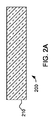
[0045]更に、感圧層は、1つ以上の異なるタイプの材料を含む構造を有してもよい。例えば、感圧層は、表面上に配置されるか又は2つの表面間に配置された感圧材料を含む。このような構成は、感圧材料及び非感圧材料の種々のセグメントを含む。図2を参照すれば、感圧層構造の多数の規範的断面が示されている。 [0045] Further, the pressure sensitive layer may have a structure comprising one or more different types of materials. For example, the pressure sensitive layer includes a pressure sensitive material disposed on a surface or disposed between two surfaces. Such a configuration includes various segments of pressure sensitive and non-pressure sensitive materials. Referring to FIG. 2, a number of exemplary cross sections of a pressure sensitive layer structure are shown.
[0046]図2Aは、感圧層200が感圧材料210の単一層で構成される実施例を示す。このような実施形態は、圧力に応答して変化するアドミティビティのような特性を有する適当な材料を含むことができる。
[0046] FIG. 2A shows an embodiment where the pressure
[0047]図2Bは、感圧層500が感圧材料212及び絶縁体214で構成される実施例を示す。この実施形態では、絶縁体214が感圧材料212の上に配置される。
[0047] FIG. 2B shows an embodiment in which the pressure
[0048]図2Cは、感圧層200が感圧材料216及び絶縁体218で構成される第2の実施例を示す。この実施形態では、絶縁体218が感圧材料216の下に配置される。
[0048] FIG. 2C shows a second embodiment in which the pressure
[0049]図2Dは、感圧層200が感圧材料220と、2つの絶縁体222及び224で構成される実施例を示す。この実施形態では、絶縁体222及び224が感圧材料220の両面に配置される。
[0049] FIG. 2D shows an embodiment in which the pressure
[0050]図2B−2Dにおいて種々の異なる材料を絶縁体として使用することができる。例えば、絶縁体は、センサの他の部分を構成する基板のような入力装置の上部又は下部要素に感圧材料を取り付けるのに使用される接着剤層を含むことができる。 [0050] A variety of different materials can be used as insulators in FIGS. 2B-2D. For example, the insulator can include an adhesive layer that is used to attach a pressure sensitive material to an upper or lower element of an input device, such as a substrate that forms another part of the sensor.
[0051]図2Eを参照すれば、感圧層200が複数の感圧セグメント228で構成される別の実施形態が示されている。一実施形態において、セグメント228は、直線的アレイ又は他のパターンで敷設される。一実施形態において、セグメント228の各々は、一次及び二次センサ電極(図示せず)の合流領域(以下に詳細に述べる)の上に配置される。別の実施形態では、セグメント228の各々は、少なくとも1つの一次センサ電極又は少なくとも1つの二次センサ電極の上に配置される。他の実施例では、一次及び二次センサ電極付近の他のエリアにセグメントが配置される。
[0051] Referring to FIG. 2E, another embodiment in which the pressure
[0052]図2F、2G及び2Hには、この実施形態の変形例が示されている。これら実施形態の各々において、感圧層は、複数の感圧セグメント228及び1つ以上の絶縁体230で構成される。例えば、図2Fは、感圧層200が複数の感圧セグメント228の下に絶縁体230を含む実施形態を示す。別の例として、図2Gは、感圧層200が複数の感圧セグメント228の上に絶縁体230を含む実施形態を示す。更に別の例として、図2Hは、感圧層200が複数の感圧セグメント228の上下の両方に絶縁体230を含む実施形態を示す。更に、前記実施形態のいずれかにおいて、絶縁体230は、複数の絶縁体セグメントで構成されてもよく、この場合に、絶縁体セグメントは、感圧セグメント228と同様のサイズ、それより小さいサイズ、又はそれより大きいサイズにすることができる。
[0052] A variation of this embodiment is shown in FIGS. 2F, 2G and 2H. In each of these embodiments, the pressure sensitive layer is comprised of a plurality of pressure
[0053]ある実施形態では、性能を向上させるために、感圧層の上、下又はその中に導電性要素が含まれてもよい。図2Iは、感圧層200が、感圧材料232の上に配置された導電性要素234で構成された実施形態を示す。図2Jは、感圧層200が、感圧材料236の下に配置された導電性要素234で構成された実施形態を示す。図2Kは、感圧層200が、感圧材料240内に配置された導電性要素242で構成された実施形態を示す。図2Lは、感圧層200が、感圧材料250の上に配置された複数の導電性要素252で構成された実施形態を示す。別の実施形態では、複数の導電性要素252が感圧材料250の下に配置される。導電性要素は、感圧層が圧力付与に応答して変形するか又はそのアドミティビティを変化させるときに、アドミタンスの変化を向上させることができる。
[0053] In some embodiments, conductive elements may be included above, below or within the pressure sensitive layer to improve performance. FIG. 2I shows an embodiment in which the pressure
[0054]従って、感圧層は、種々様々な材料から種々様々な幾何学形状で構成できることに注意されたい。また、本発明は、ここに述べた感圧層の実施例に限定されないことが意図される。むしろ、力又は圧力を受けたときに2つの至近センサ電極間の電気的アドミタンスを変化させる材料層は、いずれも、本発明の範囲内に包含される。 [0054] Thus, it should be noted that the pressure sensitive layer can be constructed from a variety of materials and in a variety of geometries. It is also intended that the present invention is not limited to the pressure-sensitive layer embodiments described herein. Rather, any material layer that changes the electrical admittance between two close sensor electrodes when subjected to force or pressure is encompassed within the scope of the present invention.
単一ノードの実施形態
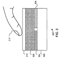
[0055]図3を参照すれば、入力装置300の側面断面図が示されている。この入力装置300は、基板層302と、一次センサ電極304と、二次センサ電極306と、感圧層308と、保護層310とを備えている。図3に示す実施形態において、一次及び二次センサ電極(例えば、電極304及び306)は、同じ層上に形成され、水平の距離により分離される。対照的に、以下に述べる他の実施形態では、一次及び二次センサ電極は、絶縁層を挟んで個別の層上に形成される。図3には、これら全ての要素が示されているが、ある実施形態では、保護層310のようなものが存在しなくてもよい。
Single node embodiment
[0055] Referring to FIG. 3, a side cross-sectional view of the
[0056]図3に示す実施形態は、種々の仕方で形成することができる。例えば、一次及び二次センサ電極304及び306は、基板層302の片面に配置されてもよい。しかしながら、他の実施形態では、電極の一部分が基板層302の両面に配置されてもよい。更に別の実施形態では、一次及び二次センサ電極304及び306は、基板の同じ面に重畳形態で配置されて、重畳するところが絶縁体で分離されてもよい。一実施形態では、一次及び二次センサ電極は、ユーザ入力のための接近検出器又は「接近ボタン」として機能するように構成することができる。図3の構成は、複数の一次センサ電極及び/又は複数の二次センサ電極を合体させて、複数次元において複数の物体を検出し且つ位置情報を決定できるスクロールストリップ、複数接近ボタンのセット及び一般的物体検出器のような入力装置を可能とするよう拡張できることに注意されたい。
[0056] The embodiment shown in FIG. 3 can be formed in various ways. For example, the primary and
[0057]一般的に、一次センサ電極304及び二次センサ電極306は、電気的アドミタンスを経て接続される。指312のような入力物体が入力装置300に接近すると(即ち、入力装置300の感知領域内に入ると)、電極間のアドミタンスを変化させる。このアドミタンスの変化を測定して、入力物体の位置情報の発生に使用することができる。
[0057] Generally, the
[0058]指312のような入力物体は、入力装置300に圧力も付与する。より詳細には、指312は、入力装置の保護層310を押すことができる。指312が保護層310を押すと、感圧層308に圧力(又は力)が加わる。この圧力は、感圧層308のアドミティビティを変化させ、電極304と306との間のアドミタンスを更に変化させる。この更なる変化の大きさを使用して、保護層310に圧力を付与する物体の圧力情報を決定することができる。
[0058] An input object such as a
[0059]1つの特定の具現化において、一次センサ電極304と二次センサ電極306との間のアドミタンスは、エラスティブアドミタンス又はトランスキャパシタンスである。トランスキャパシタンスの変化(例えば、増加又は減少)の方向(符号)は、物体のタイプに依存し、例えば、物体が導電性であるか非導電性であるかに依存する。従って、トランスキャパシタンスの変化の符号を使用して、保護層310(又は保護層310が存在しないときは感圧層308)に圧力を付与する物体が導電性物体であるか非導電性物体であるか決定することができる。変化の符号を使用して、入力物体のタイプを決定することができる。
[0059] In one particular implementation, the admittance between the
[0060]一実施形態において、感圧層308は、圧力に応答して導電率を増加するように選択され、一次センサ電極304と二次センサ電極306との間のアドミタンスは、導電性アドミタンス又はコンダクタンスである。このような実施形態では、感圧層308は、圧力が付与されないときは導電率が非常に低く、従って、本質的に絶縁体である。圧力が付与されると、圧力付与領域付近の層領域において導電率が増加する。このような導電率増加の割合及び範囲は、感圧層308に使用される材料に依存する。
[0060] In one embodiment, the pressure
[0061]種々の実施形態において、入力物体の圧力情報を決定するために、スレッシュホールドレベルが使用されてもよい。導電性物体が一次センサ電極304と二次センサ電極306の合流領域を完全にカバーするに充分な大きさである場合に、保護層310にタッチする導電性物体について考える。このような導電性物体が感圧層308のアドミティビティに変化を生じさせるに充分な圧力を付与しないときには、測定されたアドミタンスの大きさの変化のスレッシュホールドレベルとなる。測定されたアドミタンスの大きさが更に変化してこのスレッシュホールドレベルを越えると、おそらく、感圧層308のアドミタンスが変化し、それ故、導電性物体により保護層310に付与される圧力の尺度として使用することができる。
[0061] In various embodiments, threshold levels may be used to determine pressure information for an input object. Consider a conductive object that touches the
[0062]逆に、スタイラスのような非導電性物体がタッチ面付近にあるが、意義のある圧力を付与しないと、測定されたアドミタンスの大きさに意義のある変化が生じず、従って、典型的に、検出できない。しかしながら、非導電性物体が保護層310(ひいては感圧層308)に圧力を付与するときには、測定されたアドミタンスの大きさに変化を生じさせる。測定されたアドミタンスの大きさの変化の量は、非導電性物体により保護層310に付与された圧力の尺度である。まとめると、アドミタンスの値の決定を使用して、感知領域の物体に対する位置情報、圧力情報及び/又はタイプ情報、及び/又は保護層310への付与圧力を決定することができる。
[0062] Conversely, if a non-conductive object such as a stylus is near the touch surface but does not apply significant pressure, there will be no significant change in the magnitude of the measured admittance, and therefore typical Cannot be detected. However, when the non-conductive object applies pressure to the protective layer 310 (and thus the pressure sensitive layer 308), it causes a change in the measured magnitude of admittance. The amount of change in the measured admittance magnitude is a measure of the pressure applied to the
[0063]種々の異なる材料及び技術を使用して、一次センサ電極304及び二次センサ電極306を形成することができる。例えば、これら電極は、ITO(インジウムスズ酸化物)、銀又は炭素導電性インク、或いは銅のような導電性材料を使用してパターン化することができる。更に、スパッタ堆積、印刷及びエッチングを含む適当なパターン化プロセスを使用することもできる。
[0063] A variety of different materials and techniques can be used to form the
[0064]保護層310は、感圧層308上に配置される。典型的に、保護層310は、圧力又は力を感圧層308へ伝達できるようにする柔軟な材料で構成される。一実施形態において、アップリケが保護層310として使用される。一実施形態において、保護層310は、タッチ面を含み、ユーザがタッチするように設計されたタッチセンサの一部分を形成する。タッチ面として使用されるときに、保護層310は、心地よい触感又は手触りであるのが好ましい。このようなタッチ面は、ユーザに見えるので、心地よい視覚的質感があることも好ましい。保護層310は、適当な材料で形成することができる。例えば、保護層310は、MYLARという商標名で販売されているもののようなテクスチャードポリエステル材料のシートを使用して具現化することができる。ポリエステルが使用される場合には、保護層310は、適当な厚みのものでよい。多くの実施形態では、保護層は、感圧層308の上面に固定するか又は感圧層308を収容する基板に固定するためにその下面に接着剤を含む。
[0064] A
[0065]保護層310を形成するのに使用される材料は、完全に不透明から完全に透明までの範囲である。保護層310の表面は、均一な見掛けを与えるようにペイント又は着色されてもよい。それとは別に又はそれに加えて、ロゴ、レタリング、グラフィック、その組み合わせ、又は他のパターンを、ペイントの均一被覆に代わって(例えば、スクリーン印刷により)適用することもできる。多くの場合、このような装飾は、使用中の摩耗から保護されるように保護層の裏側に埋め込まれ又は適用される。保護層310に適した他の材料は、ポリエチレンテレフタレート(PET)、ポリイミド、ポリカーボネート(商標名LEXANでも販売されている)、その組み合わせ、等を含めて、あらゆる種類のプラスチックを含む。ポリカーボネートを使用する実施形態では、保護層のシート厚みは、多くの場合、約0.1mmないし約0.6mmの範囲である。
[0065] The materials used to form the
[0066]ある実施形態では、感圧層308をセンサ電極から絶縁して、感圧層がセンサ電極にオーミック接触しないようにすることが望ましい。これは、感圧層308と電極との間に充分な分離をとるようにして達成される。それとは別に又はそれに加えて、感圧層308とセンサ電極との間に絶縁層を配置することができる。以下に詳細に述べる幾つかの透明な実施形態では、一次センサ電極304及び二次センサ電極306を(感圧層から更に離れた)底部基板の下面にパターン化することもできるし、又はPETシートのような薄い絶縁材料をセンサ電極の上に(即ち、センサ電極と感圧層308との間に)配置することもできる。例えば、PETシートを、エアギャップ及び柔軟な層の下で、一次及び二次センサ電極の頂部に配置することができる。
[0066] In certain embodiments, it is desirable to insulate the pressure
[0067]図4を参照すれば、入力装置400の側面断面図が示されている。入力装置300と同様に、入力装置400は、基板層402と、一次センサ電極404と、二次センサ電極406と、感圧層408と、保護層410とを備えている。この実施形態は、電極404及び406が感圧層408と保護層410との間に位置されるという点で、図3に示す実施形態とは異なる。この実施形態は、図3を参照して上述したものとほぼ同様に動作するが、この実施形態では、圧力が一次センサ電極404及び二次センサ電極406を通して感圧層408へ伝達される。従って、入力装置は、位置及び圧力情報を決定することができ、ある実施形態では、圧力を付与する物体のタイプを決定することができる。
[0067] Referring to FIG. 4, a side cross-sectional view of the
[0068]図5を参照すれば、規範的な入力装置500の側面断面図が示されている。この入力装置500は、絶縁層502と、一次センサ電極504と、二次センサ電極506とを備えている。この実施形態は、一次センサ電極及び二次センサ電極が、絶縁層で分離された異なる層にあるという点で、図3に示す実施形態とは異なる。最終的に、保護層510が感圧層308をカバーする。
[0068] Referring to FIG. 5, a side cross-sectional view of an
多ノードの実施形態
[0069]図5に示す実施形態は、1つの一次センサ電極504及び1つの二次センサ電極506のみを備えた入力装置500である。このような実施形態では、一度に1つの物体に対してゼロ次元の位置情報と、圧力及びタイプ情報とを決定することができる。他の具現化では、複数の入力物体に対してこのような情報を同時に決定する能力を可能にするように複数の一次及び/又は複数の二次センサ電極が一緒に配列される。更に、このような装置は、典型的に、上述した一次元及び二次元の位置情報のような広範囲な位置情報を決定することができる。種々のこれらの異なる実施形態について以下に述べる。
Multi-node embodiment
[0069] The embodiment shown in FIG. 5 is an
[0070]図6を参照すれば、規範的な入力装置600の上面図が示されている。この実施形態では、入力装置600は、一次センサ電極604のセットと、二次センサ電極606のセットと、それらの上に配置された感圧層308とを備えている。このような実施形態では、一次及び二次センサ電極が実質的な電気的接続を経験するように充分物理的に接近する位置がある。これらの位置は、ここでは、合流領域と称され、個別のアドミタンスを測定できる位置を表す。この実施形態では、一次及び二次センサ電極の各交差点付近に合流領域が位置される。このような各合流領域は、入力装置600の検出ノードと考えることができる。他の実施形態では、一次センサ電極及び二次センサ電極が互いに物理的に隣接するところに合流領域が位置される。従って、合流領域及びそれに対応する検出ノードは、少なくとも1つの一次センサ電極及び少なくとも1つの二次センサ電極を織り交ぜ、噛み合わせ、クロスオーバーさせ、及び巻き合わせることを含めて、種々の実施形態において多数の仕方で形成することができる。
[0070] Referring to FIG. 6, a top view of an
[0071]図6の入力装置600は、複数の一次センサ電極及び複数の二次センサ電極を使用して複数の合流領域を形成するように、図5に示す入力装置500を拡張したものと考えられる。従って、入力装置600は、広範囲な位置情報を決定すると共に、感知領域における複数の物体、又は感知領域における大きな物体の複数の部分、例えば、手のひらの複数の点、に対する位置及び圧力情報を同時に決定するように構成される。
[0071] The
[0072]ここに示す実施形態では、一次センサ電極604のセットは、第1方向に整列され、二次センサ電極606のセットは、第2方向に整列される。より詳細には、比較的広い水平のバーは、一次センサ電極604を表す。一方、狭い垂直のバー(感圧層608により部分的に不明瞭にされた)は、二次センサ電極606を表す。一次及び二次の両センサ電極は、柔軟な又は堅個なタッチセンサ回路板を含むプリント回路の一部分として製造することができる。従って、一次及び二次センサ電極は、1つ以上の基板を含み且つ全回路アッセンブリの一部又は全部を形成する基板アッセンブリ上に配置することができる。一次及び二次センサ電極が同じ基板上に配置される場合には、それらを、基板の同じ側、基板の反対側又はその両方に配置することができる(例えば、センサ電極の一部分が基板の両側に配置される場合)。図6に示す実施形態の多くの異なる変形例が実現できることを理解されたい。例えば、感圧層608は、複数のセグメントに分割することができる。
[0072] In the illustrated embodiment, the set of
[0073]同様の実施形態による入力装置700の側面断面図である図7を参照する。この入力装置700は、一次センサ電極704のセットと、二次センサ電極706のセットと、感圧層708とを備え、これらは、全て、基板702上に形成される。一次センサ電極704及び二次センサ電極706は、まとめてセンサ電極と称される。一次センサ電極704のセットと二次センサ電極706のセットとの間に絶縁層712が形成される。この方向において、感圧層は、センサ電極の「上」に配置される。このケースでは、「装置の通常の動作中に入力物体が予想されるところへの接近」を表すために、「上」が方向として使用される。感圧層708は、少なくとも1つのセンサ電極の少なくとも一部分に重畳するように構成される。
[0073] Reference is made to FIG. 7, which is a side cross-sectional view of an
[0074]図7に示すように、一次及び二次センサ電極は、基板702上に配置される。この基板702は、種々の異なる構成及び材料、例えば、ガラス又はプラスチックを含む(1つの一般的なプラスチック基板は、PETと省略されるポリエチレンテレフタレートである)。他のタイプの材料の基板も考えられる。これらタイプの材料に加えて、基板702は、導電性材料又は非導電性材料の層のような複数の層を含むこともできる。これらの他の層は、電気的シールド、物理的保護、固定能力、等を与える。また、基板702は、大きな基板アッセンブリの一部分でもよいことに注意されたい。
[0074] As shown in FIG. 7, primary and secondary sensor electrodes are disposed on a
[0075]また、この実施形態には、感圧層708の上に位置された頂部保護層710も示されている。上述したように、ユーザは、保護層710を押して、感圧層708へ圧力を伝達することができる。前記で述べ且つ以下でも詳細に述べるように、それにより生じる一次センサ電極と二次センサ電極との間のアドミタンスの変化を使用して、保護層に加えられた圧力の尺度を与え、及び/又はその圧力を加える物体のタイプを決定することができる。
[0075] This embodiment also shows a top protective layer 710 positioned over the pressure
[0076]更に、アドミタンスの値は、一次センサ電極704及び二次センサ電極706の各合流領域に対して決定できるので、装置700は、位置及び圧力情報の配列を容易に決定することができる。複数の合流領域に対して測定されるアドミタンスのセットは、感知領域における全物体に関する情報を含む二次元アドミタンス画像として表すことができる。この二次元画像を調査することにより、「ピーク」及び「くぼみ」を探索し、指又は他の物体の位置に対応するものとして解釈することができる。これらピークの高さ及びこれらくぼみの深さは、各入力物体の圧力の独立した尺度を与えると共に、これらピーク及びくぼみの横方向程度は、物体のサイズ又は形状を決定するのに使用できる。物体の存在がピークを生じるかくぼみを生じるかは、導電率のような物体の電気的特性に依存する。従って、装置700は、入力物体の異なるタイプを容易に識別する。
[0076] Further, since the admittance value can be determined for each merged region of the
[0077]入力物体の圧力を測定する能力は、入力物体又は指が入力装置の表面を横切って偶発的に軽くかすめる場合に生じる意図的でない入力を除去する上で著しく役立つことができる。更に、導電性物体と非導電性物体との間、又は大きな物体と小さな物体との間を区別する能力は、多数の効果を発揮する。例えば、スタイラス及び手が感知領域に同時に存在するときにスタイラスを手と区別するのに使用することができる。本発明のある実施形態では、手がアドミタンス画像において大きな「くぼみ」として現われ、一方、スタイラスが鋭いピークとして現われる。本発明以前に存在する多数の従来の入力装置では、感知領域に存在する手が、スタイラスの確実な検出を妨げる。 [0077] The ability to measure the pressure of an input object can significantly help eliminate unintentional input that occurs when the input object or finger accidentally lightly grazes across the surface of the input device. Furthermore, the ability to distinguish between conductive and non-conductive objects or between large and small objects has a number of effects. For example, it can be used to distinguish the stylus from the hand when the stylus and the hand are simultaneously in the sensing area. In some embodiments of the invention, the hand appears as a large “well” in the admittance image, while the stylus appears as a sharp peak. In many conventional input devices existing prior to the present invention, the hand present in the sensing area prevents reliable detection of the stylus.
[0078]図6及び7に示す実施形態では、一次及び二次センサ電極が、各々、行及び列に配列される。更に、各一次センサ電極は、他の一次センサ電極と平行に整列され、そして各二次センサ電極は、他の二次センサ電極と平行に整列される。図6に示すように、一次センサ電極604は、二次センサ電極606と直交するよう整列されるが、90°で整列する必要はなく、45°、60°、等の他の角度で整列することができる。更に、センサ電極がまっすぐであり又は互いに平行である必要はない。ある実施形態では、一次及び二次センサ電極は、少なくとも1つの一次センサ電極が少なくとも1つの二次センサ電極と
織り合わされるように、又は少なくとも1つの一次センサ電極が少なくとも1つの二次センサ電極と織り交ぜられるように配列される。これら実施形態の詳細な実施例を図示して以下に説明する。
[0078] In the embodiment shown in FIGS. 6 and 7, the primary and secondary sensor electrodes are arranged in rows and columns, respectively. Further, each primary sensor electrode is aligned in parallel with the other primary sensor electrodes, and each secondary sensor electrode is aligned in parallel with the other secondary sensor electrodes. As shown in FIG. 6, the
[0079]図7に示す実施形態では、一次センサ電極704と二次センサ電極706との間に絶縁層712が配置され、各々が個別の層を表している。別の実施形態では、一次センサ電極の少なくとも一部分を、二次センサ電極の少なくとも一部分と同じ層においてパターン化することができる。このような実施形態では、一次センサ電極及び二次センサ電極が互いに交差する必要がある場合に、望ましからぬ電気的接触を防止するために、一次センサ電極と二次センサ電極との間の交点に適宜にジャンパーを使用することができる。一次及び二次の両センサ電極が同じ層に形成された電極構造の実施例が図3及び4に示されている。
[0079] In the embodiment shown in FIG. 7, an insulating layer 712 is disposed between the
[0080]また、これら実施形態の多くにおいて、感圧層は、複数の一次及び二次センサ電極に重畳する単一構造体として具現化できることにも注意されたい。逆に、このような装置は、複数の感圧層で具現化することもできる。1つの特定の実施形態において、感圧層は、一次センサ電極と二次センサ電極との間の各合流領域(例えば、交差位置)の上に形成された複数の感圧セグメントで構成される。 [0080] It should also be noted that in many of these embodiments, the pressure sensitive layer can be embodied as a single structure overlying a plurality of primary and secondary sensor electrodes. Conversely, such a device can also be implemented with a plurality of pressure sensitive layers. In one particular embodiment, the pressure sensitive layer is comprised of a plurality of pressure sensitive segments formed on each merged region (eg, an intersection location) between the primary sensor electrode and the secondary sensor electrode.
[0081]図8を参照すれば、入力装置800の側面断面図が示されている。図7の入力装置と同様に、この入力装置800は、基板層802と、一次センサ電極804のセットと、二次センサ電極806のセットと、感圧層808と、保護層810とを備えている。この実施形態でも、一次センサ電極804及び二次センサ電極806は、異なる層上にあって、絶縁層812によって分離されている。しかしながら、この実施形態は、センサ電極804及び806が感圧層808と保護層810との間に位置するという点で、図7の実施形態とは異なる。また、このような実施形態は、図6及び7を参照して上述したのとほぼ同様に動作するが、この実施形態では、圧力が一次センサ電極804及び二次センサ電極806を通して感圧層808へ伝達される。従って、入力装置は、位置及び圧力情報を決定することができ、また、ある実施形態では、圧力を付与する物体のタイプを決定することができる。
[0081] Referring to FIG. 8, a side cross-sectional view of the
[0082]図9を参照すれば、入力装置900の側面断面図が示されている。前記装置と同様に、この入力装置900は、基板層902と、一次センサ電極904のセットと、二次センサ電極906のセットと、感圧層908と、保護層910とを備えている。また、この実施形態でも、一次センサ電極904及び二次センサ電極906は、異なる層上にある。しかしながら、この実施形態では、センサ電極の2つのセットが感圧層908により分離される。この実施例において、入力物体がセンサに接近したときに、一次及び二次センサ電極を使用して、入力物体の位置情報を決定することができる。更に、入力物体が保護層910に圧力を加えるときに、その圧力は、感圧層へ伝達され、一次センサ電極と二次センサ電極との間のアドミタンスが変化する。更に、このような実施形態は、図6及び7を参照して上述したものと一般的に同様に動作することができる。従って、入力装置は、位置及び圧力情報を決定することができ、また、ある実施形態では、圧力を加える物体のタイプを決定することができる。
[0082] Referring to FIG. 9, a side cross-sectional view of the
[0083]図10を参照すれば、入力装置1000の側面断面図が示されている。この入力装置は、基板層1002と、一次センサ電極1004のセットと、二次センサ電極1006のセットと、感圧層1008と、感圧材料1016と、電気的に浮動の導電性要素1014のセットと、保護層1010と、絶縁層1012とを備えている。上述したように、この実施形態では、一次センサ電極1004及び二次センサ電極1006は、異なる層にあって、感圧層1008の下に位置されている。しかしながら、この実施形態では、電気的に浮動の導電性要素1014のセットは、感圧材料1016の上に位置される。別の実施形態では、電気的に浮動の導電性要素1010が二次センサ電極1006と感圧材料1016との間に位置される。
[0083] Referring to FIG. 10, a side cross-sectional view of the
[0084]少なくとも1つの一次センサ電極及び少なくとも1つの二次センサ電極を合体するここに述べる全ての実施形態では、「一次」及び「二次」の呼称は、任意である。これら実施形態の各々において「一次」及び「二次」の表現を入れ替えることで、別の等しく有用な実施形態のセットを得ることができる。 [0084] In all embodiments described herein that combine at least one primary sensor electrode and at least one secondary sensor electrode, the designations "primary" and "secondary" are arbitrary. By swapping the terms “primary” and “secondary” in each of these embodiments, another set of equally useful embodiments can be obtained.
自己アドミタンスの実施形態
[0085]図11は、感圧層1108が単一のセンサ電極1104の上に配置された実施形態の断面図である。センサ電極1104は、基板1102の表面上に配置される。一実施形態において、センサ電極1104は、ユーザの指のような入力物体の存在に応答する接近ボタンとして機能するように構成される。別の実施形態では、複数のセンサ電極を複数の接近ボタンとして機能するように構成することもできるし、又は電極のアレイを一次元の位置情報を決定するためのスクロールストリップとして使用することもできる。センサ1100は、センサ電極1104と入力物体1112の間のアドミタンスの変化を測定することにより入力物体の存在を検出することができる。センサ電極1104と入力物体1112との間のこのアドミタンスは、時々、「自己アドミタンス」として知られている。
Self-admittance embodiments
FIG. 11 is a cross-sectional view of an embodiment in which a pressure
[0086]一実施形態において、センサ電極と入力物体との間のアドミタンスの変化を測定するために、センサ電極へ電気的信号が送られ(driven)、その信号の特性が測定される。例えば、センサ電極へ電圧信号を送り(drive)、それにより生じる電流を測定することができる。測定された特性(例えば、測定された電流)から、アドミタンスの変化を決定することができる。入力物体1112が保護層1110に向かって移動するときに、自己アドミタンス測定値が変化し、従って、物体の位置の決定を与える。更に、入力物体1112が保護層1110に圧力を加えると、感圧層1108がそのアドミティビティを変化させ、自己アドミタンス測定値を更に変化させ、従って、付与された圧力の決定を与える。
[0086] In one embodiment, in order to measure the change in admittance between the sensor electrode and the input object, an electrical signal is driven to the sensor electrode and the characteristics of the signal are measured. For example, a voltage signal can be sent to the sensor electrode and the resulting current can be measured. From the measured characteristic (eg, measured current), the change in admittance can be determined. As the
[0087]図12は、感圧層1208が一次センサ電極1204のセット及び二次センサ電極1206のセットの上に配置された実施形態の断面図である。動作中に、センサ1200は、一次センサ電極1204の各々と入力物体1212との間、及び二次センサ電極1206の各々と入力物体1212との間のアドミタンスの変化を決定することにより、入力物体1212に対する位置情報及び/又は圧力情報を検出するように構成される。図12の各センサ電極のアドミタンスは、図11のセンサ電極について上述したのと同様に、一度に1つづつ、又は1つ以上のグループで同時に、決定することができる。
[0087] FIG. 12 is a cross-sectional view of an embodiment in which a pressure
[0088]この実施形態では、入力物体1212は、一次及び二次センサ電極(1204及び1206)の少なくとも1つに電気的に接続されて、アドミタンスに変化を生じさせ、従って、入力物体に対する位置情報の決定をなす。入力物体1212が保護層1210に圧力を加えると、感圧層1208がそのアドミティビティを変化させて、アドミタンスを更に変化させ、従って、加えた圧力の決定をなす。
[0088] In this embodiment, the input object 1212 is electrically connected to at least one of the primary and secondary sensor electrodes (1204 and 1206) to cause a change in admittance and thus position information for the input object. Make a decision. When the input object 1212 applies pressure to the
[0089]更に、アドミタンスの値は、入力物体1212と、一次センサ電極1204及び二次センサ電極1206の各々との間で決定できるので、装置1200は、多次元の位置及び圧力情報を容易に決定する。測定されたアドミタンスは、センサ装置1200の第1及び第2の軸に沿った2つの一次元プロフィールとして表すことができる。これらの一次元プロフィールは、各軸に沿ったアドミタンスの変化のシルエット又は投影であると考えられ、入力物体の位置及び/又は圧力を決定するのに使用できる。各プロフィールは、指又は他の物体の位置を表すものとして解釈することができる。これらプロフィールの高さは、各入力物体により付与される圧力に関連した情報を与え、また、これらプロフィールの横方向の程度は、物体のサイズ又は形状に関連した情報を与えることができる。ある実施形態では、入力物体(1つ又は複数)を検出するためにセンサ電極の1つのセットに電気的信号で駆動される間に、センサ電極の他のセットをガード信号で駆動して、センサ電極の2つのセット間の寄生結合の影響を減少することができる。
[0089] Further, since the admittance value can be determined between the input object 1212 and each of the
結論
[0090]従って、本発明の実施形態は、タッチ面に付与される圧力に応答して1つ以上の電気的アドミタンスを変化させるように構成された感圧層を使用することにより入力装置の性能改善を促進する装置及び方法を提供する。
Conclusion
[0090] Accordingly, embodiments of the present invention provide input device performance by using a pressure sensitive layer configured to change one or more electrical admittances in response to pressure applied to the touch surface. An apparatus and method for promoting improvement is provided.
[0091]ある実施形態では、1つ以上の一次センサ電極のセット及び1つ以上の二次センサ電極のセットを含む複数のセンサ電極を備えた入力装置が提供される。一次センサ電極は、二次センサ電極に電気的に接続されて、1つ以上のアドミタンスのセットを形成する。1つのこのような実施形態において、センサ電極とタッチ面との間に感圧層が配置される。 [0091] In an embodiment, an input device is provided that includes a plurality of sensor electrodes including a set of one or more primary sensor electrodes and a set of one or more secondary sensor electrodes. The primary sensor electrode is electrically connected to the secondary sensor electrode to form a set of one or more admittances. In one such embodiment, a pressure sensitive layer is disposed between the sensor electrode and the touch surface.
[0092]他の実施形態において、入力物体に電気的に接続されて1つ以上のアドミタンスのセットを形成する1つ以上のセンサ電極のセットを備えた入力装置が提供される。このような1つの実施形態では、センサ電極とタッチ面との間に感圧層が配置される。 [0092] In another embodiment, an input device is provided comprising a set of one or more sensor electrodes that are electrically connected to an input object to form a set of one or more admittances. In one such embodiment, a pressure sensitive layer is disposed between the sensor electrode and the touch surface.
100・・・電子システム、114・・・スタイラス、116・・・入力装置、118・・・感知領域、119・・・処理システム、120・・・ボタン、200・・・感圧領域、210・・・感圧材料、212:感圧材料、214・・・絶縁体、216・・・感圧材料、218・・・絶縁体、220・・・感圧材料、222、224・・・絶縁体、228・・・感圧セグメント、230・・・絶縁体、232・・・感圧材料、234・・・導電性要素、236・・・感圧材料、238・・・導電性要素、240・・・感圧材料、252・・・導電性要素、250・・・感圧材料、300・・・入力装置、302…基板層、304・・・一次センサ電極、306・・・二次センサ電極、308・・・感圧層、310・・・保護層、312・・・指、400・・・入力装置、402…基板層、404・・・一次センサ電極、406・・・二次センサ電極、408・・・感圧層、410・・・保護層、500・・・入力装置、502・・・絶縁層、504・・・一次センサ電極、506・・・二次センサ電極、510・・・保護層、600・・・入力装置、604・・・一次センサ電極のセット、606・・・二次センサ電極のセット
DESCRIPTION OF
Claims (6)
複数の一次センサ電極からなるセット及び複数の二次センサ電極からなるセットを含む複数のセンサ電極であり、前記一次センサ電極の各々が前記二次センサ電極の少なくとも1つに電気的に接続されて複数のアドミタンスからなるセットを形成する、複数のセンサ電極と、
タッチ面と、
前記タッチ面と前記複数のセンサ電極との間に配置された感圧層であり、前記タッチ面に付与される圧力に応答して前記アドミタンスの少なくとも1つを変化させるように構成された感圧層と、
を備える入力装置。 An input device for sensing an input object in a sensing area,
A plurality of sensor electrodes including a set of a plurality of primary sensor electrodes and a set of a plurality of secondary sensor electrodes, each of the primary sensor electrodes being electrically connected to at least one of the secondary sensor electrodes. A plurality of sensor electrodes forming a set of a plurality of admittances;
Touch surface,
A pressure-sensitive layer disposed between the touch surface and the plurality of sensor electrodes, the pressure-sensitive layer configured to change at least one of the admittances in response to a pressure applied to the touch surface. Layers,
An input device comprising:
この処理システムは、更に、前記アドミタンスの値に基づく前記感知領域における前記入力物体の位置情報と、少なくとも1つの前記値の変化に基づく前記入力物体の圧力情報と、のうちの少なくとも1つを決定するように構成される、請求項1に記載の入力装置。 Further comprising a processing system connected to the primary sensor electrode and the secondary sensor electrode and configured to determine a value of the admittance;
The processing system further includes a positional information of the input object in the sensing area rather based on the value of the admittance, and pressure information of said input object based on a change of at least one of said values, at least one of The input device of claim 1, wherein the input device is configured to determine.
前記複数のセンサ電極の第2部分である、複数の二次センサ電極からなるセットで前記信号を受信し、前記一次センサ電極の各々は前記二次センサ電極の少なくとも1つに電気的に接続されて複数のアドミタンスからなるセットを形成し、タッチ面と前記複数のセンサ電極との間に感圧層が配置され、この感圧層は、前記タッチ面上の入力物体によって前記感圧層に付与される圧力に応答して前記アドミタンスの少なくとも1つを変化させるように構成され、
前記受信した信号から前記アドミタンスの値を決定し、
前記アドミタンスの前記値から前記タッチ面上の前記入力物体に対する位置情報を決定し、
前記位置情報を表す出力を与える、
ように構成される処理システム。 Sending a signal to a set of a plurality of primary sensor electrodes, which is a first part of a plurality of sensor electrodes;
Receiving the signal in a set of a plurality of secondary sensor electrodes, which is a second portion of the plurality of sensor electrodes, each of the primary sensor electrodes being electrically connected to at least one of the secondary sensor electrodes; Forming a set of a plurality of admittances, and a pressure sensitive layer is disposed between the touch surface and the plurality of sensor electrodes, and the pressure sensitive layer is applied to the pressure sensitive layer by an input object on the touch surface. Configured to change at least one of the admittances in response to applied pressure;
Determining the value of the admittance from the received signal;
Determining position information for the input object on the touch surface from the value of the admittance ;
Giving an output representing the position information;
Processing system configured as follows.
前記アドミタンスの前記値から前記タッチ面上の前記入力物体に対する圧力情報を決定し、
前記圧力情報を表す出力を与える、
ように更に構成される、請求項5に記載の処理システム。
The processing system
Determining pressure information for the input object on the touch surface from the value of the admittance ;
Providing an output representative of the pressure information;
The processing system of claim 5 , further configured as follows.
Applications Claiming Priority (5)
| Application Number | Priority Date | Filing Date | Title |
|---|---|---|---|
| US18380909P | 2009-06-03 | 2009-06-03 | |
| US61/183,809 | 2009-06-03 | ||
| US12/792,578 | 2010-06-02 | ||
| US12/792,578 US9383881B2 (en) | 2009-06-03 | 2010-06-02 | Input device and method with pressure-sensitive layer |
| PCT/US2010/037279 WO2010141737A2 (en) | 2009-06-03 | 2010-06-03 | Input device and method with pressure-sensitive layer |
Publications (3)
| Publication Number | Publication Date |
|---|---|
| JP2012529126A JP2012529126A (en) | 2012-11-15 |
| JP2012529126A5 JP2012529126A5 (en) | 2013-07-18 |
| JP5679235B2 true JP5679235B2 (en) | 2015-03-04 |
Family
ID=43298523
Family Applications (1)
| Application Number | Title | Priority Date | Filing Date |
|---|---|---|---|
| JP2012514135A Expired - Fee Related JP5679235B2 (en) | 2009-06-03 | 2010-06-03 | Input device and method with pressure sensitive layer |
Country Status (5)
| Country | Link |
|---|---|
| US (1) | US9383881B2 (en) |
| EP (1) | EP2438501A4 (en) |
| JP (1) | JP5679235B2 (en) |
| CN (1) | CN102449583B (en) |
| WO (1) | WO2010141737A2 (en) |
Families Citing this family (476)
| Publication number | Priority date | Publication date | Assignee | Title |
|---|---|---|---|---|
| US9060770B2 (en) | 2003-05-20 | 2015-06-23 | Ethicon Endo-Surgery, Inc. | Robotically-driven surgical instrument with E-beam driver |
| US20070084897A1 (en) | 2003-05-20 | 2007-04-19 | Shelton Frederick E Iv | Articulating surgical stapling instrument incorporating a two-piece e-beam firing mechanism |
| US8215531B2 (en) | 2004-07-28 | 2012-07-10 | Ethicon Endo-Surgery, Inc. | Surgical stapling instrument having a medical substance dispenser |
| US11896225B2 (en) | 2004-07-28 | 2024-02-13 | Cilag Gmbh International | Staple cartridge comprising a pan |
| US11246590B2 (en) | 2005-08-31 | 2022-02-15 | Cilag Gmbh International | Staple cartridge including staple drivers having different unfired heights |
| US9237891B2 (en) | 2005-08-31 | 2016-01-19 | Ethicon Endo-Surgery, Inc. | Robotically-controlled surgical stapling devices that produce formed staples having different lengths |
| US10159482B2 (en) | 2005-08-31 | 2018-12-25 | Ethicon Llc | Fastener cartridge assembly comprising a fixed anvil and different staple heights |
| US11484312B2 (en) | 2005-08-31 | 2022-11-01 | Cilag Gmbh International | Staple cartridge comprising a staple driver arrangement |
| US7669746B2 (en) | 2005-08-31 | 2010-03-02 | Ethicon Endo-Surgery, Inc. | Staple cartridges for forming staples having differing formed staple heights |
| US7934630B2 (en) | 2005-08-31 | 2011-05-03 | Ethicon Endo-Surgery, Inc. | Staple cartridges for forming staples having differing formed staple heights |
| US20070106317A1 (en) | 2005-11-09 | 2007-05-10 | Shelton Frederick E Iv | Hydraulically and electrically actuated articulation joints for surgical instruments |
| US20110290856A1 (en) | 2006-01-31 | 2011-12-01 | Ethicon Endo-Surgery, Inc. | Robotically-controlled surgical instrument with force-feedback capabilities |
| US7753904B2 (en) | 2006-01-31 | 2010-07-13 | Ethicon Endo-Surgery, Inc. | Endoscopic surgical instrument with a handle that can articulate with respect to the shaft |
| US8186555B2 (en) | 2006-01-31 | 2012-05-29 | Ethicon Endo-Surgery, Inc. | Motor-driven surgical cutting and fastening instrument with mechanical closure system |
| US11224427B2 (en) | 2006-01-31 | 2022-01-18 | Cilag Gmbh International | Surgical stapling system including a console and retraction assembly |
| US7845537B2 (en) | 2006-01-31 | 2010-12-07 | Ethicon Endo-Surgery, Inc. | Surgical instrument having recording capabilities |
| US20120292367A1 (en) | 2006-01-31 | 2012-11-22 | Ethicon Endo-Surgery, Inc. | Robotically-controlled end effector |
| US8708213B2 (en) | 2006-01-31 | 2014-04-29 | Ethicon Endo-Surgery, Inc. | Surgical instrument having a feedback system |
| US20110024477A1 (en) | 2009-02-06 | 2011-02-03 | Hall Steven G | Driven Surgical Stapler Improvements |
| US11793518B2 (en) | 2006-01-31 | 2023-10-24 | Cilag Gmbh International | Powered surgical instruments with firing system lockout arrangements |
| US11278279B2 (en) | 2006-01-31 | 2022-03-22 | Cilag Gmbh International | Surgical instrument assembly |
| US8820603B2 (en) | 2006-01-31 | 2014-09-02 | Ethicon Endo-Surgery, Inc. | Accessing data stored in a memory of a surgical instrument |
| US8992422B2 (en) | 2006-03-23 | 2015-03-31 | Ethicon Endo-Surgery, Inc. | Robotically-controlled endoscopic accessory channel |
| US8322455B2 (en) | 2006-06-27 | 2012-12-04 | Ethicon Endo-Surgery, Inc. | Manually driven surgical cutting and fastening instrument |
| US10568652B2 (en) | 2006-09-29 | 2020-02-25 | Ethicon Llc | Surgical staples having attached drivers of different heights and stapling instruments for deploying the same |
| US11291441B2 (en) | 2007-01-10 | 2022-04-05 | Cilag Gmbh International | Surgical instrument with wireless communication between control unit and remote sensor |
| US8652120B2 (en) | 2007-01-10 | 2014-02-18 | Ethicon Endo-Surgery, Inc. | Surgical instrument with wireless communication between control unit and sensor transponders |
| US8684253B2 (en) | 2007-01-10 | 2014-04-01 | Ethicon Endo-Surgery, Inc. | Surgical instrument with wireless communication between a control unit of a robotic system and remote sensor |
| US11039836B2 (en) | 2007-01-11 | 2021-06-22 | Cilag Gmbh International | Staple cartridge for use with a surgical stapling instrument |
| US8701958B2 (en) | 2007-01-11 | 2014-04-22 | Ethicon Endo-Surgery, Inc. | Curved end effector for a surgical stapling device |
| US8727197B2 (en) | 2007-03-15 | 2014-05-20 | Ethicon Endo-Surgery, Inc. | Staple cartridge cavity configuration with cooperative surgical staple |
| US11672531B2 (en) | 2007-06-04 | 2023-06-13 | Cilag Gmbh International | Rotary drive systems for surgical instruments |
| US8931682B2 (en) | 2007-06-04 | 2015-01-13 | Ethicon Endo-Surgery, Inc. | Robotically-controlled shaft based rotary drive systems for surgical instruments |
| US7753245B2 (en) | 2007-06-22 | 2010-07-13 | Ethicon Endo-Surgery, Inc. | Surgical stapling instruments |
| US11849941B2 (en) | 2007-06-29 | 2023-12-26 | Cilag Gmbh International | Staple cartridge having staple cavities extending at a transverse angle relative to a longitudinal cartridge axis |
| US7866527B2 (en) | 2008-02-14 | 2011-01-11 | Ethicon Endo-Surgery, Inc. | Surgical stapling apparatus with interlockable firing system |
| US8758391B2 (en) | 2008-02-14 | 2014-06-24 | Ethicon Endo-Surgery, Inc. | Interchangeable tools for surgical instruments |
| US9179912B2 (en) | 2008-02-14 | 2015-11-10 | Ethicon Endo-Surgery, Inc. | Robotically-controlled motorized surgical cutting and fastening instrument |
| BRPI0901282A2 (en) | 2008-02-14 | 2009-11-17 | Ethicon Endo Surgery Inc | surgical cutting and fixation instrument with rf electrodes |
| US8573465B2 (en) | 2008-02-14 | 2013-11-05 | Ethicon Endo-Surgery, Inc. | Robotically-controlled surgical end effector system with rotary actuated closure systems |
| US7819298B2 (en) | 2008-02-14 | 2010-10-26 | Ethicon Endo-Surgery, Inc. | Surgical stapling apparatus with control features operable with one hand |
| US8636736B2 (en) | 2008-02-14 | 2014-01-28 | Ethicon Endo-Surgery, Inc. | Motorized surgical cutting and fastening instrument |
| US9615826B2 (en) | 2010-09-30 | 2017-04-11 | Ethicon Endo-Surgery, Llc | Multiple thickness implantable layers for surgical stapling devices |
| US9018030B2 (en) | 2008-03-20 | 2015-04-28 | Symbol Technologies, Inc. | Transparent force sensor and method of fabrication |
| US9386983B2 (en) | 2008-09-23 | 2016-07-12 | Ethicon Endo-Surgery, Llc | Robotically-controlled motorized surgical instrument |
| US9005230B2 (en) | 2008-09-23 | 2015-04-14 | Ethicon Endo-Surgery, Inc. | Motorized surgical instrument |
| US11648005B2 (en) | 2008-09-23 | 2023-05-16 | Cilag Gmbh International | Robotically-controlled motorized surgical instrument with an end effector |
| US8210411B2 (en) | 2008-09-23 | 2012-07-03 | Ethicon Endo-Surgery, Inc. | Motor-driven surgical cutting instrument |
| US8608045B2 (en) | 2008-10-10 | 2013-12-17 | Ethicon Endo-Sugery, Inc. | Powered surgical cutting and stapling apparatus with manually retractable firing system |
| US8517239B2 (en) | 2009-02-05 | 2013-08-27 | Ethicon Endo-Surgery, Inc. | Surgical stapling instrument comprising a magnetic element driver |
| JP2012517287A (en) | 2009-02-06 | 2012-08-02 | エシコン・エンド−サージェリィ・インコーポレイテッド | Improvement of driven surgical stapler |
| JP2011017626A (en) * | 2009-07-09 | 2011-01-27 | Sony Corp | Mechanical quantity detection member and mechanical quantity detection apparatus |
| US8988191B2 (en) | 2009-08-27 | 2015-03-24 | Symbol Technologies, Inc. | Systems and methods for pressure-based authentication of an input on a touch screen |
| US9891757B2 (en) * | 2009-12-21 | 2018-02-13 | Synaptics Incorporated | Elastive sensing |
| US8220688B2 (en) | 2009-12-24 | 2012-07-17 | Ethicon Endo-Surgery, Inc. | Motor-driven surgical cutting instrument with electric actuator directional control assembly |
| US8851354B2 (en) | 2009-12-24 | 2014-10-07 | Ethicon Endo-Surgery, Inc. | Surgical cutting instrument that analyzes tissue thickness |
| DE102011006344B4 (en) | 2010-03-31 | 2020-03-12 | Joyson Safety Systems Acquisition Llc | Occupant measurement system |
| JP5805974B2 (en) | 2010-03-31 | 2015-11-10 | ティーケー ホールディングス,インコーポレーテッド | Steering wheel sensor |
| DE102011006649B4 (en) | 2010-04-02 | 2018-05-03 | Tk Holdings Inc. | Steering wheel with hand sensors |
| US20110273394A1 (en) * | 2010-05-10 | 2011-11-10 | Symbol Technologies, Inc. | Methods and apparatus for a transparent and flexible force-sensitive touch panel |
| CN103154812B (en) | 2010-07-30 | 2016-08-10 | 小利兰·斯坦福大学托管委员会 | Conducting film |
| US8783543B2 (en) | 2010-07-30 | 2014-07-22 | Ethicon Endo-Surgery, Inc. | Tissue acquisition arrangements and methods for surgical stapling devices |
| US8963874B2 (en) | 2010-07-31 | 2015-02-24 | Symbol Technologies, Inc. | Touch screen rendering system and method of operation thereof |
| US9281415B2 (en) | 2010-09-10 | 2016-03-08 | The Board Of Trustees Of The Leland Stanford Junior University | Pressure sensing apparatuses and methods |
| US9386988B2 (en) | 2010-09-30 | 2016-07-12 | Ethicon End-Surgery, LLC | Retainer assembly including a tissue thickness compensator |
| US11925354B2 (en) | 2010-09-30 | 2024-03-12 | Cilag Gmbh International | Staple cartridge comprising staples positioned within a compressible portion thereof |
| US11812965B2 (en) | 2010-09-30 | 2023-11-14 | Cilag Gmbh International | Layer of material for a surgical end effector |
| US9700317B2 (en) | 2010-09-30 | 2017-07-11 | Ethicon Endo-Surgery, Llc | Fastener cartridge comprising a releasable tissue thickness compensator |
| US11298125B2 (en) | 2010-09-30 | 2022-04-12 | Cilag Gmbh International | Tissue stapler having a thickness compensator |
| US9629814B2 (en) | 2010-09-30 | 2017-04-25 | Ethicon Endo-Surgery, Llc | Tissue thickness compensator configured to redistribute compressive forces |
| US9113865B2 (en) | 2010-09-30 | 2015-08-25 | Ethicon Endo-Surgery, Inc. | Staple cartridge comprising a layer |
| US9351730B2 (en) | 2011-04-29 | 2016-05-31 | Ethicon Endo-Surgery, Llc | Tissue thickness compensator comprising channels |
| US10945731B2 (en) | 2010-09-30 | 2021-03-16 | Ethicon Llc | Tissue thickness compensator comprising controlled release and expansion |
| US8695866B2 (en) | 2010-10-01 | 2014-04-15 | Ethicon Endo-Surgery, Inc. | Surgical instrument having a power control circuit |
| US8618428B2 (en) | 2010-12-14 | 2013-12-31 | Synaptics Incorporated | System and method for determining object information using an estimated rigid motion response |
| US9201185B2 (en) | 2011-02-04 | 2015-12-01 | Microsoft Technology Licensing, Llc | Directional backlighting for display panels |
| JP5689705B2 (en) * | 2011-02-10 | 2015-03-25 | 任天堂株式会社 | Information processing system, information processing program, information processing device, input device, and information processing method |
| AU2012250197B2 (en) | 2011-04-29 | 2017-08-10 | Ethicon Endo-Surgery, Inc. | Staple cartridge comprising staples positioned within a compressible portion thereof |
| US11207064B2 (en) | 2011-05-27 | 2021-12-28 | Cilag Gmbh International | Automated end effector component reloading system for use with a robotic system |
| US9072535B2 (en) | 2011-05-27 | 2015-07-07 | Ethicon Endo-Surgery, Inc. | Surgical stapling instruments with rotatable staple deployment arrangements |
| US8607651B2 (en) | 2011-09-30 | 2013-12-17 | Sensitronics, LLC | Hybrid capacitive force sensors |
| US9256311B2 (en) * | 2011-10-28 | 2016-02-09 | Atmel Corporation | Flexible touch sensor |
| US9052414B2 (en) | 2012-02-07 | 2015-06-09 | Microsoft Technology Licensing, Llc | Virtual image device |
| US9354748B2 (en) | 2012-02-13 | 2016-05-31 | Microsoft Technology Licensing, Llc | Optical stylus interaction |
| US8749529B2 (en) | 2012-03-01 | 2014-06-10 | Microsoft Corporation | Sensor-in-pixel display system with near infrared filter |
| US9426905B2 (en) | 2012-03-02 | 2016-08-23 | Microsoft Technology Licensing, Llc | Connection device for computing devices |
| DE112013001251T5 (en) * | 2012-03-02 | 2014-11-27 | Tokai Rubber Industries, Ltd. | hybrid sensor |
| US9460029B2 (en) | 2012-03-02 | 2016-10-04 | Microsoft Technology Licensing, Llc | Pressure sensitive keys |
| USRE48963E1 (en) | 2012-03-02 | 2022-03-08 | Microsoft Technology Licensing, Llc | Connection device for computing devices |
| US9298236B2 (en) | 2012-03-02 | 2016-03-29 | Microsoft Technology Licensing, Llc | Multi-stage power adapter configured to provide a first power level upon initial connection of the power adapter to the host device and a second power level thereafter upon notification from the host device to the power adapter |
| US8873227B2 (en) | 2012-03-02 | 2014-10-28 | Microsoft Corporation | Flexible hinge support layer |
| US9075566B2 (en) | 2012-03-02 | 2015-07-07 | Microsoft Technoogy Licensing, LLC | Flexible hinge spine |
| US9360893B2 (en) | 2012-03-02 | 2016-06-07 | Microsoft Technology Licensing, Llc | Input device writing surface |
| US9870066B2 (en) | 2012-03-02 | 2018-01-16 | Microsoft Technology Licensing, Llc | Method of manufacturing an input device |
| US9064654B2 (en) | 2012-03-02 | 2015-06-23 | Microsoft Technology Licensing, Llc | Method of manufacturing an input device |
| RU2644272C2 (en) | 2012-03-28 | 2018-02-08 | Этикон Эндо-Серджери, Инк. | Limitation node with tissue thickness compensator |
| JP6305979B2 (en) | 2012-03-28 | 2018-04-04 | エシコン・エンド−サージェリィ・インコーポレイテッドEthicon Endo−Surgery,Inc. | Tissue thickness compensator with multiple layers |
| BR112014024098B1 (en) | 2012-03-28 | 2021-05-25 | Ethicon Endo-Surgery, Inc. | staple cartridge |
| US9665214B2 (en) * | 2012-03-29 | 2017-05-30 | Synaptics Incorporated | System and methods for determining object information using selectively floated electrodes |
| WO2013154720A1 (en) | 2012-04-13 | 2013-10-17 | Tk Holdings Inc. | Pressure sensor including a pressure sensitive material for use with control systems and methods of using the same |
| US20130300590A1 (en) | 2012-05-14 | 2013-11-14 | Paul Henry Dietz | Audio Feedback |
| US10031556B2 (en) | 2012-06-08 | 2018-07-24 | Microsoft Technology Licensing, Llc | User experience adaptation |
| US8947353B2 (en) | 2012-06-12 | 2015-02-03 | Microsoft Corporation | Photosensor array gesture detection |
| US9019615B2 (en) | 2012-06-12 | 2015-04-28 | Microsoft Technology Licensing, Llc | Wide field-of-view virtual image projector |
| US9459160B2 (en) | 2012-06-13 | 2016-10-04 | Microsoft Technology Licensing, Llc | Input device sensor configuration |
| US9684382B2 (en) | 2012-06-13 | 2017-06-20 | Microsoft Technology Licensing, Llc | Input device configuration having capacitive and pressure sensors |
| US9073123B2 (en) | 2012-06-13 | 2015-07-07 | Microsoft Technology Licensing, Llc | Housing vents |
| US9101358B2 (en) | 2012-06-15 | 2015-08-11 | Ethicon Endo-Surgery, Inc. | Articulatable surgical instrument comprising a firing drive |
| US9256089B2 (en) | 2012-06-15 | 2016-02-09 | Microsoft Technology Licensing, Llc | Object-detecting backlight unit |
| WO2013192539A1 (en) | 2012-06-21 | 2013-12-27 | Nextinput, Inc. | Wafer level mems force dies |
| BR112014032776B1 (en) | 2012-06-28 | 2021-09-08 | Ethicon Endo-Surgery, Inc | SURGICAL INSTRUMENT SYSTEM AND SURGICAL KIT FOR USE WITH A SURGICAL INSTRUMENT SYSTEM |
| US9408606B2 (en) | 2012-06-28 | 2016-08-09 | Ethicon Endo-Surgery, Llc | Robotically powered surgical device with manually-actuatable reversing system |
| JP6290201B2 (en) | 2012-06-28 | 2018-03-07 | エシコン・エンド−サージェリィ・インコーポレイテッドEthicon Endo−Surgery,Inc. | Lockout for empty clip cartridge |
| US20140001231A1 (en) | 2012-06-28 | 2014-01-02 | Ethicon Endo-Surgery, Inc. | Firing system lockout arrangements for surgical instruments |
| US11202631B2 (en) | 2012-06-28 | 2021-12-21 | Cilag Gmbh International | Stapling assembly comprising a firing lockout |
| US9282974B2 (en) | 2012-06-28 | 2016-03-15 | Ethicon Endo-Surgery, Llc | Empty clip cartridge lockout |
| US9289256B2 (en) | 2012-06-28 | 2016-03-22 | Ethicon Endo-Surgery, Llc | Surgical end effectors having angled tissue-contacting surfaces |
| EP2870445A1 (en) | 2012-07-05 | 2015-05-13 | Ian Campbell | Microelectromechanical load sensor and methods of manufacturing the same |
| US9355345B2 (en) | 2012-07-23 | 2016-05-31 | Microsoft Technology Licensing, Llc | Transparent tags with encoded data |
| US8964379B2 (en) | 2012-08-20 | 2015-02-24 | Microsoft Corporation | Switchable magnetic lock |
| US9696223B2 (en) | 2012-09-17 | 2017-07-04 | Tk Holdings Inc. | Single layer force sensor |
| US9152173B2 (en) | 2012-10-09 | 2015-10-06 | Microsoft Technology Licensing, Llc | Transparent display device |
| US8654030B1 (en) | 2012-10-16 | 2014-02-18 | Microsoft Corporation | Antenna placement |
| WO2014059618A1 (en) | 2012-10-17 | 2014-04-24 | Microsoft Corporation | Graphic formation via material ablation |
| WO2014059625A1 (en) | 2012-10-17 | 2014-04-24 | Microsoft Corporation | Metal alloy injection molding overflows |
| EP2908970B1 (en) | 2012-10-17 | 2018-01-03 | Microsoft Technology Licensing, LLC | Metal alloy injection molding protrusions |
| US8952892B2 (en) | 2012-11-01 | 2015-02-10 | Microsoft Corporation | Input location correction tables for input panels |
| US8786767B2 (en) | 2012-11-02 | 2014-07-22 | Microsoft Corporation | Rapid synchronized lighting and shuttering |
| US9513748B2 (en) | 2012-12-13 | 2016-12-06 | Microsoft Technology Licensing, Llc | Combined display panel circuit |
| US10817096B2 (en) | 2014-02-06 | 2020-10-27 | Apple Inc. | Force sensor incorporated into display |
| US10168814B2 (en) | 2012-12-14 | 2019-01-01 | Apple Inc. | Force sensing based on capacitance changes |
| US9141259B2 (en) | 2013-01-21 | 2015-09-22 | International Business Machines Corporation | Pressure navigation on a touch sensitive user interface |
| US9176538B2 (en) | 2013-02-05 | 2015-11-03 | Microsoft Technology Licensing, Llc | Input device configurations |
| EP2954392B1 (en) | 2013-02-08 | 2022-12-28 | Apple Inc. | Force determination based on capacitive sensing |
| US10578499B2 (en) | 2013-02-17 | 2020-03-03 | Microsoft Technology Licensing, Llc | Piezo-actuated virtual buttons for touch surfaces |
| RU2669463C2 (en) | 2013-03-01 | 2018-10-11 | Этикон Эндо-Серджери, Инк. | Surgical instrument with soft stop |
| BR112015021098B1 (en) | 2013-03-01 | 2022-02-15 | Ethicon Endo-Surgery, Inc | COVERAGE FOR A JOINT JOINT AND SURGICAL INSTRUMENT |
| US9638835B2 (en) | 2013-03-05 | 2017-05-02 | Microsoft Technology Licensing, Llc | Asymmetric aberration correcting lens |
| US9883860B2 (en) | 2013-03-14 | 2018-02-06 | Ethicon Llc | Interchangeable shaft assemblies for use with a surgical instrument |
| US9629629B2 (en) | 2013-03-14 | 2017-04-25 | Ethicon Endo-Surgey, LLC | Control systems for surgical instruments |
| US9851828B2 (en) | 2013-03-15 | 2017-12-26 | Apple Inc. | Touch force deflection sensor |
| US9304549B2 (en) | 2013-03-28 | 2016-04-05 | Microsoft Technology Licensing, Llc | Hinge mechanism for rotatable component attachment |
| US10136887B2 (en) | 2013-04-16 | 2018-11-27 | Ethicon Llc | Drive system decoupling arrangement for a surgical instrument |
| BR112015026109B1 (en) | 2013-04-16 | 2022-02-22 | Ethicon Endo-Surgery, Inc | surgical instrument |
| US9552777B2 (en) | 2013-05-10 | 2017-01-24 | Microsoft Technology Licensing, Llc | Phase control backlight |
| US9671889B1 (en) | 2013-07-25 | 2017-06-06 | Apple Inc. | Input member with capacitive sensor |
| CN105103102B (en) * | 2013-08-16 | 2018-12-21 | 株式会社和冠 | Indication body detection device and instruction body detecting method |
| WO2015022938A1 (en) | 2013-08-16 | 2015-02-19 | 株式会社ワコム | Pointing device detection sensor and pointing device detection device |
| US9924942B2 (en) | 2013-08-23 | 2018-03-27 | Ethicon Llc | Motor-powered articulatable surgical instruments |
| MX369362B (en) | 2013-08-23 | 2019-11-06 | Ethicon Endo Surgery Llc | Firing member retraction devices for powered surgical instruments. |
| US9007343B1 (en) | 2013-10-01 | 2015-04-14 | Synaptics Incorporated | Display guarding techniques |
| US8823399B1 (en) * | 2013-10-07 | 2014-09-02 | Cypress Semiconductor Corporation | Detect and differentiate touches from different size conductive objects on a capacitive button |
| KR101712346B1 (en) * | 2014-09-19 | 2017-03-22 | 주식회사 하이딥 | Touch input device |
| US9483118B2 (en) | 2013-12-27 | 2016-11-01 | Rovi Guides, Inc. | Methods and systems for selecting media guidance functions based on tactile attributes of a user input |
| US9448631B2 (en) | 2013-12-31 | 2016-09-20 | Microsoft Technology Licensing, Llc | Input device haptics and pressure sensing |
| CN105934661B (en) | 2014-01-13 | 2019-11-05 | 触控解决方案股份有限公司 | Miniature reinforcing wafer-level MEMS force snesor |
| US9317072B2 (en) | 2014-01-28 | 2016-04-19 | Microsoft Technology Licensing, Llc | Hinge mechanism with preset positions |
| US9962161B2 (en) | 2014-02-12 | 2018-05-08 | Ethicon Llc | Deliverable surgical instrument |
| WO2015123322A1 (en) | 2014-02-12 | 2015-08-20 | Apple Inc. | Force determination employing sheet sensor and capacitive array |
| US9759854B2 (en) | 2014-02-17 | 2017-09-12 | Microsoft Technology Licensing, Llc | Input device outer layer and backlighting |
| US10126807B2 (en) | 2014-02-18 | 2018-11-13 | Cambridge Touch Technologies Ltd. | Dynamic switching of power modes for touch screens using force touch |
| US10120420B2 (en) | 2014-03-21 | 2018-11-06 | Microsoft Technology Licensing, Llc | Lockable display and techniques enabling use of lockable displays |
| US9820738B2 (en) | 2014-03-26 | 2017-11-21 | Ethicon Llc | Surgical instrument comprising interactive systems |
| BR112016021943B1 (en) | 2014-03-26 | 2022-06-14 | Ethicon Endo-Surgery, Llc | SURGICAL INSTRUMENT FOR USE BY AN OPERATOR IN A SURGICAL PROCEDURE |
| US9804618B2 (en) | 2014-03-26 | 2017-10-31 | Ethicon Llc | Systems and methods for controlling a segmented circuit |
| JP6532889B2 (en) | 2014-04-16 | 2019-06-19 | エシコン エルエルシーEthicon LLC | Fastener cartridge assembly and staple holder cover arrangement |
| BR112016023825B1 (en) | 2014-04-16 | 2022-08-02 | Ethicon Endo-Surgery, Llc | STAPLE CARTRIDGE FOR USE WITH A SURGICAL STAPLER AND STAPLE CARTRIDGE FOR USE WITH A SURGICAL INSTRUMENT |
| CN106456176B (en) | 2014-04-16 | 2019-06-28 | 伊西康内外科有限责任公司 | Fastener cartridge including the extension with various configuration |
| US11185330B2 (en) | 2014-04-16 | 2021-11-30 | Cilag Gmbh International | Fastener cartridge assemblies and staple retainer cover arrangements |
| US20150297222A1 (en) | 2014-04-16 | 2015-10-22 | Ethicon Endo-Surgery, Inc. | Fastener cartridges including extensions having different configurations |
| US10198123B2 (en) | 2014-04-21 | 2019-02-05 | Apple Inc. | Mitigating noise in capacitive sensor |
| US9703431B2 (en) * | 2014-06-03 | 2017-07-11 | Synaptics Incorporated | Noise detection and mitigation for capacitive sensing devices |
| US9841850B2 (en) * | 2014-06-16 | 2017-12-12 | Synaptics Incorporated | Device and method for proximity sensing with force imaging |
| US10324733B2 (en) | 2014-07-30 | 2019-06-18 | Microsoft Technology Licensing, Llc | Shutdown notifications |
| US11311294B2 (en) | 2014-09-05 | 2022-04-26 | Cilag Gmbh International | Powered medical device including measurement of closure state of jaws |
| BR112017004361B1 (en) | 2014-09-05 | 2023-04-11 | Ethicon Llc | ELECTRONIC SYSTEM FOR A SURGICAL INSTRUMENT |
| US10135242B2 (en) | 2014-09-05 | 2018-11-20 | Ethicon Llc | Smart cartridge wake up operation and data retention |
| US9424048B2 (en) | 2014-09-15 | 2016-08-23 | Microsoft Technology Licensing, Llc | Inductive peripheral retention device |
| US10105142B2 (en) | 2014-09-18 | 2018-10-23 | Ethicon Llc | Surgical stapler with plurality of cutting elements |
| US11523821B2 (en) | 2014-09-26 | 2022-12-13 | Cilag Gmbh International | Method for creating a flexible staple line |
| MX2017003960A (en) | 2014-09-26 | 2017-12-04 | Ethicon Llc | Surgical stapling buttresses and adjunct materials. |
| US9447620B2 (en) | 2014-09-30 | 2016-09-20 | Microsoft Technology Licensing, Llc | Hinge mechanism with multiple preset positions |
| US10076325B2 (en) | 2014-10-13 | 2018-09-18 | Ethicon Llc | Surgical stapling apparatus comprising a tissue stop |
| US9924944B2 (en) | 2014-10-16 | 2018-03-27 | Ethicon Llc | Staple cartridge comprising an adjunct material |
| US9501167B2 (en) | 2014-10-22 | 2016-11-22 | Synaptics Incorporated | Scanned piezoelectric touch sensor device |
| US11141153B2 (en) | 2014-10-29 | 2021-10-12 | Cilag Gmbh International | Staple cartridges comprising driver arrangements |
| US10517594B2 (en) | 2014-10-29 | 2019-12-31 | Ethicon Llc | Cartridge assemblies for surgical staplers |
| US9844376B2 (en) | 2014-11-06 | 2017-12-19 | Ethicon Llc | Staple cartridge comprising a releasable adjunct material |
| US10736636B2 (en) | 2014-12-10 | 2020-08-11 | Ethicon Llc | Articulatable surgical instrument system |
| US9519360B2 (en) | 2014-12-11 | 2016-12-13 | Synaptics Incorporated | Palm rejection visualization for passive stylus |
| RU2703684C2 (en) | 2014-12-18 | 2019-10-21 | ЭТИКОН ЭНДО-СЕРДЖЕРИ, ЭлЭлСи | Surgical instrument with anvil which is selectively movable relative to staple cartridge around discrete fixed axis |
| US10085748B2 (en) | 2014-12-18 | 2018-10-02 | Ethicon Llc | Locking arrangements for detachable shaft assemblies with articulatable surgical end effectors |
| US9844375B2 (en) | 2014-12-18 | 2017-12-19 | Ethicon Llc | Drive arrangements for articulatable surgical instruments |
| US9844374B2 (en) | 2014-12-18 | 2017-12-19 | Ethicon Llc | Surgical instrument systems comprising an articulatable end effector and means for adjusting the firing stroke of a firing member |
| US9987000B2 (en) | 2014-12-18 | 2018-06-05 | Ethicon Llc | Surgical instrument assembly comprising a flexible articulation system |
| US10004501B2 (en) | 2014-12-18 | 2018-06-26 | Ethicon Llc | Surgical instruments with improved closure arrangements |
| US9495052B2 (en) | 2014-12-19 | 2016-11-15 | Synaptics Incorporated | Active input device support for a capacitive sensing device |
| US9791970B2 (en) * | 2014-12-22 | 2017-10-17 | Synaptics Incorporated | Method and system for dual node sensing |
| US11154301B2 (en) | 2015-02-27 | 2021-10-26 | Cilag Gmbh International | Modular stapling assembly |
| US10687806B2 (en) | 2015-03-06 | 2020-06-23 | Ethicon Llc | Adaptive tissue compression techniques to adjust closure rates for multiple tissue types |
| US10617412B2 (en) | 2015-03-06 | 2020-04-14 | Ethicon Llc | System for detecting the mis-insertion of a staple cartridge into a surgical stapler |
| US9993248B2 (en) | 2015-03-06 | 2018-06-12 | Ethicon Endo-Surgery, Llc | Smart sensors with local signal processing |
| JP2020121162A (en) | 2015-03-06 | 2020-08-13 | エシコン エルエルシーEthicon LLC | Time dependent evaluation of sensor data to determine stability element, creep element and viscoelastic element of measurement |
| US10052044B2 (en) | 2015-03-06 | 2018-08-21 | Ethicon Llc | Time dependent evaluation of sensor data to determine stability, creep, and viscoelastic elements of measures |
| US9901342B2 (en) | 2015-03-06 | 2018-02-27 | Ethicon Endo-Surgery, Llc | Signal and power communication system positioned on a rotatable shaft |
| US10441279B2 (en) | 2015-03-06 | 2019-10-15 | Ethicon Llc | Multiple level thresholds to modify operation of powered surgical instruments |
| US10006937B2 (en) | 2015-03-06 | 2018-06-26 | Apple Inc. | Capacitive sensors for electronic devices and methods of forming the same |
| US10245033B2 (en) | 2015-03-06 | 2019-04-02 | Ethicon Llc | Surgical instrument comprising a lockable battery housing |
| US10390825B2 (en) | 2015-03-31 | 2019-08-27 | Ethicon Llc | Surgical instrument with progressive rotary drive systems |
| US10222889B2 (en) | 2015-06-03 | 2019-03-05 | Microsoft Technology Licensing, Llc | Force inputs and cursor control |
| US10416799B2 (en) | 2015-06-03 | 2019-09-17 | Microsoft Technology Licensing, Llc | Force sensing and inadvertent input control of an input device |
| US10466119B2 (en) | 2015-06-10 | 2019-11-05 | Nextinput, Inc. | Ruggedized wafer level MEMS force sensor with a tolerance trench |
| US9752361B2 (en) | 2015-06-18 | 2017-09-05 | Microsoft Technology Licensing, Llc | Multistage hinge |
| US9864415B2 (en) | 2015-06-30 | 2018-01-09 | Microsoft Technology Licensing, Llc | Multistage friction hinge |
| US9715301B2 (en) | 2015-08-04 | 2017-07-25 | Apple Inc. | Proximity edge sensing |
| US11058425B2 (en) | 2015-08-17 | 2021-07-13 | Ethicon Llc | Implantable layers for a surgical instrument |
| US10261619B2 (en) | 2015-08-31 | 2019-04-16 | Synaptics Incorporated | Estimating force applied by an input object to a touch sensor |
| KR101742584B1 (en) * | 2015-09-02 | 2017-06-01 | 주식회사 하이딥 | Touch pressure detectable touch input device |
| CN106502481A (en) * | 2015-09-08 | 2017-03-15 | 深圳莱宝高科技股份有限公司 | A kind of touch control display apparatus and preparation method thereof |
| EP3320415A4 (en) * | 2015-09-22 | 2019-03-06 | Immersion Corporation | Pressure-based haptics |
| US10105139B2 (en) | 2015-09-23 | 2018-10-23 | Ethicon Llc | Surgical stapler having downstream current-based motor control |
| US10238386B2 (en) | 2015-09-23 | 2019-03-26 | Ethicon Llc | Surgical stapler having motor control based on an electrical parameter related to a motor current |
| US10299878B2 (en) | 2015-09-25 | 2019-05-28 | Ethicon Llc | Implantable adjunct systems for determining adjunct skew |
| US10037112B2 (en) | 2015-09-30 | 2018-07-31 | Synaptics Incorporated | Sensing an active device'S transmission using timing interleaved with display updates |
| US11890015B2 (en) | 2015-09-30 | 2024-02-06 | Cilag Gmbh International | Compressible adjunct with crossing spacer fibers |
| US10980539B2 (en) | 2015-09-30 | 2021-04-20 | Ethicon Llc | Implantable adjunct comprising bonded layers |
| US10561420B2 (en) | 2015-09-30 | 2020-02-18 | Ethicon Llc | Tubular absorbable constructs |
| US10285699B2 (en) | 2015-09-30 | 2019-05-14 | Ethicon Llc | Compressible adjunct |
| US10368865B2 (en) | 2015-12-30 | 2019-08-06 | Ethicon Llc | Mechanisms for compensating for drivetrain failure in powered surgical instruments |
| US10265068B2 (en) | 2015-12-30 | 2019-04-23 | Ethicon Llc | Surgical instruments with separable motors and motor control circuits |
| US10292704B2 (en) | 2015-12-30 | 2019-05-21 | Ethicon Llc | Mechanisms for compensating for battery pack failure in powered surgical instruments |
| US10061385B2 (en) | 2016-01-22 | 2018-08-28 | Microsoft Technology Licensing, Llc | Haptic feedback for a touch input device |
| BR112018016098B1 (en) | 2016-02-09 | 2023-02-23 | Ethicon Llc | SURGICAL INSTRUMENT |
| US11213293B2 (en) | 2016-02-09 | 2022-01-04 | Cilag Gmbh International | Articulatable surgical instruments with single articulation link arrangements |
| US10448948B2 (en) | 2016-02-12 | 2019-10-22 | Ethicon Llc | Mechanisms for compensating for drivetrain failure in powered surgical instruments |
| US11224426B2 (en) | 2016-02-12 | 2022-01-18 | Cilag Gmbh International | Mechanisms for compensating for drivetrain failure in powered surgical instruments |
| US20170242581A1 (en) * | 2016-02-23 | 2017-08-24 | Myscript | System and method for multiple input management |
| US10007343B2 (en) | 2016-03-31 | 2018-06-26 | Apple Inc. | Force sensor in an input device |
| US10344797B2 (en) | 2016-04-05 | 2019-07-09 | Microsoft Technology Licensing, Llc | Hinge with multiple preset positions |
| US10426467B2 (en) | 2016-04-15 | 2019-10-01 | Ethicon Llc | Surgical instrument with detection sensors |
| US11607239B2 (en) | 2016-04-15 | 2023-03-21 | Cilag Gmbh International | Systems and methods for controlling a surgical stapling and cutting instrument |
| US10357247B2 (en) | 2016-04-15 | 2019-07-23 | Ethicon Llc | Surgical instrument with multiple program responses during a firing motion |
| US10456137B2 (en) | 2016-04-15 | 2019-10-29 | Ethicon Llc | Staple formation detection mechanisms |
| US10828028B2 (en) | 2016-04-15 | 2020-11-10 | Ethicon Llc | Surgical instrument with multiple program responses during a firing motion |
| US10492783B2 (en) | 2016-04-15 | 2019-12-03 | Ethicon, Llc | Surgical instrument with improved stop/start control during a firing motion |
| US11179150B2 (en) | 2016-04-15 | 2021-11-23 | Cilag Gmbh International | Systems and methods for controlling a surgical stapling and cutting instrument |
| US10335145B2 (en) | 2016-04-15 | 2019-07-02 | Ethicon Llc | Modular surgical instrument with configurable operating mode |
| US11317917B2 (en) | 2016-04-18 | 2022-05-03 | Cilag Gmbh International | Surgical stapling system comprising a lockable firing assembly |
| US20170296173A1 (en) | 2016-04-18 | 2017-10-19 | Ethicon Endo-Surgery, Llc | Method for operating a surgical instrument |
| US10478181B2 (en) | 2016-04-18 | 2019-11-19 | Ethicon Llc | Cartridge lockout arrangements for rotary powered surgical cutting and stapling instruments |
| CN106095160A (en) * | 2016-05-26 | 2016-11-09 | 武汉华星光电技术有限公司 | Pressure transducer and pressure touch panel |
| CN109690460A (en) * | 2016-09-07 | 2019-04-26 | 触觉实验室股份有限公司 | Pressure and shear sensors |
| US10037057B2 (en) | 2016-09-22 | 2018-07-31 | Microsoft Technology Licensing, Llc | Friction hinge |
| KR101958323B1 (en) * | 2016-11-22 | 2019-03-15 | 주식회사 하이딥 | Pressure sensing unit and touch input device including the same |
| US11419606B2 (en) | 2016-12-21 | 2022-08-23 | Cilag Gmbh International | Shaft assembly comprising a clutch configured to adapt the output of a rotary firing member to two different systems |
| US10617414B2 (en) | 2016-12-21 | 2020-04-14 | Ethicon Llc | Closure member arrangements for surgical instruments |
| US20180168625A1 (en) | 2016-12-21 | 2018-06-21 | Ethicon Endo-Surgery, Llc | Surgical stapling instruments with smart staple cartridges |
| CN110099619B (en) | 2016-12-21 | 2022-07-15 | 爱惜康有限责任公司 | Lockout device for surgical end effector and replaceable tool assembly |
| US10856868B2 (en) | 2016-12-21 | 2020-12-08 | Ethicon Llc | Firing member pin configurations |
| US10893864B2 (en) | 2016-12-21 | 2021-01-19 | Ethicon | Staple cartridges and arrangements of staples and staple cavities therein |
| US20180168615A1 (en) | 2016-12-21 | 2018-06-21 | Ethicon Endo-Surgery, Llc | Method of deforming staples from two different types of staple cartridges with the same surgical stapling instrument |
| US10588632B2 (en) | 2016-12-21 | 2020-03-17 | Ethicon Llc | Surgical end effectors and firing members thereof |
| US10758229B2 (en) | 2016-12-21 | 2020-09-01 | Ethicon Llc | Surgical instrument comprising improved jaw control |
| US10675026B2 (en) | 2016-12-21 | 2020-06-09 | Ethicon Llc | Methods of stapling tissue |
| US20180168608A1 (en) | 2016-12-21 | 2018-06-21 | Ethicon Endo-Surgery, Llc | Surgical instrument system comprising an end effector lockout and a firing assembly lockout |
| US11134942B2 (en) | 2016-12-21 | 2021-10-05 | Cilag Gmbh International | Surgical stapling instruments and staple-forming anvils |
| US10588630B2 (en) | 2016-12-21 | 2020-03-17 | Ethicon Llc | Surgical tool assemblies with closure stroke reduction features |
| JP7010956B2 (en) | 2016-12-21 | 2022-01-26 | エシコン エルエルシー | How to staple tissue |
| BR112019011947A2 (en) | 2016-12-21 | 2019-10-29 | Ethicon Llc | surgical stapling systems |
| US10675025B2 (en) | 2016-12-21 | 2020-06-09 | Ethicon Llc | Shaft assembly comprising separately actuatable and retractable systems |
| US10682138B2 (en) | 2016-12-21 | 2020-06-16 | Ethicon Llc | Bilaterally asymmetric staple forming pocket pairs |
| US10517595B2 (en) | 2016-12-21 | 2019-12-31 | Ethicon Llc | Jaw actuated lock arrangements for preventing advancement of a firing member in a surgical end effector unless an unfired cartridge is installed in the end effector |
| WO2018148510A1 (en) | 2017-02-09 | 2018-08-16 | Nextinput, Inc. | Integrated piezoresistive and piezoelectric fusion force sensor |
| EP3580539A4 (en) | 2017-02-09 | 2020-11-25 | Nextinput, Inc. | Integrated digital force sensors and related methods of manufacture |
| CN106940603B (en) * | 2017-03-15 | 2019-08-13 | 上海大学 | A kind of touch sensing and preparation method |
| US10922515B2 (en) * | 2017-04-14 | 2021-02-16 | Synaptics Incorporated | Integrated fingerprint and force sensor |
| US10888321B2 (en) | 2017-06-20 | 2021-01-12 | Ethicon Llc | Systems and methods for controlling velocity of a displacement member of a surgical stapling and cutting instrument |
| US11517325B2 (en) | 2017-06-20 | 2022-12-06 | Cilag Gmbh International | Closed loop feedback control of motor velocity of a surgical stapling and cutting instrument based on measured displacement distance traveled over a specified time interval |
| USD890784S1 (en) | 2017-06-20 | 2020-07-21 | Ethicon Llc | Display panel with changeable graphical user interface |
| US11382638B2 (en) | 2017-06-20 | 2022-07-12 | Cilag Gmbh International | Closed loop feedback control of motor velocity of a surgical stapling and cutting instrument based on measured time over a specified displacement distance |
| US11071554B2 (en) | 2017-06-20 | 2021-07-27 | Cilag Gmbh International | Closed loop feedback control of motor velocity of a surgical stapling and cutting instrument based on magnitude of velocity error measurements |
| US11653914B2 (en) | 2017-06-20 | 2023-05-23 | Cilag Gmbh International | Systems and methods for controlling motor velocity of a surgical stapling and cutting instrument according to articulation angle of end effector |
| US10779820B2 (en) | 2017-06-20 | 2020-09-22 | Ethicon Llc | Systems and methods for controlling motor speed according to user input for a surgical instrument |
| US10980537B2 (en) | 2017-06-20 | 2021-04-20 | Ethicon Llc | Closed loop feedback control of motor velocity of a surgical stapling and cutting instrument based on measured time over a specified number of shaft rotations |
| US10881399B2 (en) | 2017-06-20 | 2021-01-05 | Ethicon Llc | Techniques for adaptive control of motor velocity of a surgical stapling and cutting instrument |
| US10646220B2 (en) | 2017-06-20 | 2020-05-12 | Ethicon Llc | Systems and methods for controlling displacement member velocity for a surgical instrument |
| US11090046B2 (en) | 2017-06-20 | 2021-08-17 | Cilag Gmbh International | Systems and methods for controlling displacement member motion of a surgical stapling and cutting instrument |
| US10307170B2 (en) | 2017-06-20 | 2019-06-04 | Ethicon Llc | Method for closed loop control of motor velocity of a surgical stapling and cutting instrument |
| US10993716B2 (en) | 2017-06-27 | 2021-05-04 | Ethicon Llc | Surgical anvil arrangements |
| US11324503B2 (en) | 2017-06-27 | 2022-05-10 | Cilag Gmbh International | Surgical firing member arrangements |
| US10856869B2 (en) | 2017-06-27 | 2020-12-08 | Ethicon Llc | Surgical anvil arrangements |
| US11266405B2 (en) | 2017-06-27 | 2022-03-08 | Cilag Gmbh International | Surgical anvil manufacturing methods |
| US20180368844A1 (en) | 2017-06-27 | 2018-12-27 | Ethicon Llc | Staple forming pocket arrangements |
| EP3420947B1 (en) | 2017-06-28 | 2022-05-25 | Cilag GmbH International | Surgical instrument comprising selectively actuatable rotatable couplers |
| US11564686B2 (en) | 2017-06-28 | 2023-01-31 | Cilag Gmbh International | Surgical shaft assemblies with flexible interfaces |
| US11678880B2 (en) | 2017-06-28 | 2023-06-20 | Cilag Gmbh International | Surgical instrument comprising a shaft including a housing arrangement |
| US11246592B2 (en) | 2017-06-28 | 2022-02-15 | Cilag Gmbh International | Surgical instrument comprising an articulation system lockable to a frame |
| US11020114B2 (en) | 2017-06-28 | 2021-06-01 | Cilag Gmbh International | Surgical instruments with articulatable end effector with axially shortened articulation joint configurations |
| US10765427B2 (en) | 2017-06-28 | 2020-09-08 | Ethicon Llc | Method for articulating a surgical instrument |
| USD906355S1 (en) | 2017-06-28 | 2020-12-29 | Ethicon Llc | Display screen or portion thereof with a graphical user interface for a surgical instrument |
| US10903685B2 (en) | 2017-06-28 | 2021-01-26 | Ethicon Llc | Surgical shaft assemblies with slip ring assemblies forming capacitive channels |
| US10716614B2 (en) | 2017-06-28 | 2020-07-21 | Ethicon Llc | Surgical shaft assemblies with slip ring assemblies with increased contact pressure |
| US11259805B2 (en) | 2017-06-28 | 2022-03-01 | Cilag Gmbh International | Surgical instrument comprising firing member supports |
| US10898183B2 (en) | 2017-06-29 | 2021-01-26 | Ethicon Llc | Robotic surgical instrument with closed loop feedback techniques for advancement of closure member during firing |
| US10932772B2 (en) | 2017-06-29 | 2021-03-02 | Ethicon Llc | Methods for closed loop velocity control for robotic surgical instrument |
| US11007022B2 (en) | 2017-06-29 | 2021-05-18 | Ethicon Llc | Closed loop velocity control techniques based on sensed tissue parameters for robotic surgical instrument |
| KR102357420B1 (en) * | 2017-07-06 | 2022-02-04 | 삼성디스플레이 주식회사 | Touch sensor and display device including the touch sensor |
| US11221263B2 (en) | 2017-07-19 | 2022-01-11 | Nextinput, Inc. | Microelectromechanical force sensor having a strain transfer layer arranged on the sensor die |
| US11423686B2 (en) | 2017-07-25 | 2022-08-23 | Qorvo Us, Inc. | Integrated fingerprint and force sensor |
| WO2019023552A1 (en) | 2017-07-27 | 2019-01-31 | Nextinput, Inc. | A wafer bonded piezoresistive and piezoelectric force sensor and related methods of manufacture |
| US11471155B2 (en) | 2017-08-03 | 2022-10-18 | Cilag Gmbh International | Surgical system bailout |
| US11304695B2 (en) | 2017-08-03 | 2022-04-19 | Cilag Gmbh International | Surgical system shaft interconnection |
| US11944300B2 (en) | 2017-08-03 | 2024-04-02 | Cilag Gmbh International | Method for operating a surgical system bailout |
| USD917500S1 (en) | 2017-09-29 | 2021-04-27 | Ethicon Llc | Display screen or portion thereof with graphical user interface |
| USD907648S1 (en) | 2017-09-29 | 2021-01-12 | Ethicon Llc | Display screen or portion thereof with animated graphical user interface |
| US11399829B2 (en) | 2017-09-29 | 2022-08-02 | Cilag Gmbh International | Systems and methods of initiating a power shutdown mode for a surgical instrument |
| US10765429B2 (en) | 2017-09-29 | 2020-09-08 | Ethicon Llc | Systems and methods for providing alerts according to the operational state of a surgical instrument |
| US10743872B2 (en) | 2017-09-29 | 2020-08-18 | Ethicon Llc | System and methods for controlling a display of a surgical instrument |
| USD907647S1 (en) | 2017-09-29 | 2021-01-12 | Ethicon Llc | Display screen or portion thereof with animated graphical user interface |
| US11579028B2 (en) | 2017-10-17 | 2023-02-14 | Nextinput, Inc. | Temperature coefficient of offset compensation for force sensor and strain gauge |
| US11134944B2 (en) | 2017-10-30 | 2021-10-05 | Cilag Gmbh International | Surgical stapler knife motion controls |
| US11090075B2 (en) | 2017-10-30 | 2021-08-17 | Cilag Gmbh International | Articulation features for surgical end effector |
| US10842490B2 (en) | 2017-10-31 | 2020-11-24 | Ethicon Llc | Cartridge body design with force reduction based on firing completion |
| US10779903B2 (en) | 2017-10-31 | 2020-09-22 | Ethicon Llc | Positive shaft rotation lock activated by jaw closure |
| US11385108B2 (en) | 2017-11-02 | 2022-07-12 | Nextinput, Inc. | Sealed force sensor with etch stop layer |
| US11874185B2 (en) | 2017-11-16 | 2024-01-16 | Nextinput, Inc. | Force attenuator for force sensor |
| CN107930121B (en) * | 2017-12-12 | 2020-09-01 | 苏州蜗牛数字科技股份有限公司 | Method and device for controlling game target to move according to input device type |
| US10779826B2 (en) | 2017-12-15 | 2020-09-22 | Ethicon Llc | Methods of operating surgical end effectors |
| US11033267B2 (en) | 2017-12-15 | 2021-06-15 | Ethicon Llc | Systems and methods of controlling a clamping member firing rate of a surgical instrument |
| US10966718B2 (en) | 2017-12-15 | 2021-04-06 | Ethicon Llc | Dynamic clamping assemblies with improved wear characteristics for use in connection with electromechanical surgical instruments |
| US10743875B2 (en) | 2017-12-15 | 2020-08-18 | Ethicon Llc | Surgical end effectors with jaw stiffener arrangements configured to permit monitoring of firing member |
| US11006955B2 (en) | 2017-12-15 | 2021-05-18 | Ethicon Llc | End effectors with positive jaw opening features for use with adapters for electromechanical surgical instruments |
| US10828033B2 (en) | 2017-12-15 | 2020-11-10 | Ethicon Llc | Handheld electromechanical surgical instruments with improved motor control arrangements for positioning components of an adapter coupled thereto |
| CN108108071B (en) * | 2017-12-15 | 2021-10-01 | 京东方科技集团股份有限公司 | Touch panel and preparation method thereof, and touch display screen and preparation method thereof |
| US10687813B2 (en) | 2017-12-15 | 2020-06-23 | Ethicon Llc | Adapters with firing stroke sensing arrangements for use in connection with electromechanical surgical instruments |
| US10779825B2 (en) | 2017-12-15 | 2020-09-22 | Ethicon Llc | Adapters with end effector position sensing and control arrangements for use in connection with electromechanical surgical instruments |
| US11071543B2 (en) | 2017-12-15 | 2021-07-27 | Cilag Gmbh International | Surgical end effectors with clamping assemblies configured to increase jaw aperture ranges |
| US10743874B2 (en) | 2017-12-15 | 2020-08-18 | Ethicon Llc | Sealed adapters for use with electromechanical surgical instruments |
| US11197670B2 (en) | 2017-12-15 | 2021-12-14 | Cilag Gmbh International | Surgical end effectors with pivotal jaws configured to touch at their respective distal ends when fully closed |
| US10869666B2 (en) | 2017-12-15 | 2020-12-22 | Ethicon Llc | Adapters with control systems for controlling multiple motors of an electromechanical surgical instrument |
| US11020112B2 (en) | 2017-12-19 | 2021-06-01 | Ethicon Llc | Surgical tools configured for interchangeable use with different controller interfaces |
| USD910847S1 (en) | 2017-12-19 | 2021-02-16 | Ethicon Llc | Surgical instrument assembly |
| US10729509B2 (en) | 2017-12-19 | 2020-08-04 | Ethicon Llc | Surgical instrument comprising closure and firing locking mechanism |
| US10716565B2 (en) | 2017-12-19 | 2020-07-21 | Ethicon Llc | Surgical instruments with dual articulation drivers |
| US10835330B2 (en) | 2017-12-19 | 2020-11-17 | Ethicon Llc | Method for determining the position of a rotatable jaw of a surgical instrument attachment assembly |
| US11045270B2 (en) | 2017-12-19 | 2021-06-29 | Cilag Gmbh International | Robotic attachment comprising exterior drive actuator |
| US11179151B2 (en) | 2017-12-21 | 2021-11-23 | Cilag Gmbh International | Surgical instrument comprising a display |
| CN111670013A (en) * | 2017-12-21 | 2020-09-15 | 爱惜康有限责任公司 | Surgical instrument including a display |
| US11129680B2 (en) | 2017-12-21 | 2021-09-28 | Cilag Gmbh International | Surgical instrument comprising a projector |
| US11076853B2 (en) | 2017-12-21 | 2021-08-03 | Cilag Gmbh International | Systems and methods of displaying a knife position during transection for a surgical instrument |
| US11311290B2 (en) | 2017-12-21 | 2022-04-26 | Cilag Gmbh International | Surgical instrument comprising an end effector dampener |
| CN108279805B (en) * | 2018-01-31 | 2022-03-25 | 北京小米移动软件有限公司 | Protective film detection method, device and storage medium |
| US11207065B2 (en) | 2018-08-20 | 2021-12-28 | Cilag Gmbh International | Method for fabricating surgical stapler anvils |
| US11045192B2 (en) | 2018-08-20 | 2021-06-29 | Cilag Gmbh International | Fabricating techniques for surgical stapler anvils |
| US10842492B2 (en) | 2018-08-20 | 2020-11-24 | Ethicon Llc | Powered articulatable surgical instruments with clutching and locking arrangements for linking an articulation drive system to a firing drive system |
| US11039834B2 (en) | 2018-08-20 | 2021-06-22 | Cilag Gmbh International | Surgical stapler anvils with staple directing protrusions and tissue stability features |
| US11083458B2 (en) | 2018-08-20 | 2021-08-10 | Cilag Gmbh International | Powered surgical instruments with clutching arrangements to convert linear drive motions to rotary drive motions |
| USD914878S1 (en) | 2018-08-20 | 2021-03-30 | Ethicon Llc | Surgical instrument anvil |
| US10912559B2 (en) | 2018-08-20 | 2021-02-09 | Ethicon Llc | Reinforced deformable anvil tip for surgical stapler anvil |
| US11291440B2 (en) | 2018-08-20 | 2022-04-05 | Cilag Gmbh International | Method for operating a powered articulatable surgical instrument |
| US10856870B2 (en) | 2018-08-20 | 2020-12-08 | Ethicon Llc | Switching arrangements for motor powered articulatable surgical instruments |
| US11324501B2 (en) | 2018-08-20 | 2022-05-10 | Cilag Gmbh International | Surgical stapling devices with improved closure members |
| US11253256B2 (en) | 2018-08-20 | 2022-02-22 | Cilag Gmbh International | Articulatable motor powered surgical instruments with dedicated articulation motor arrangements |
| US10779821B2 (en) | 2018-08-20 | 2020-09-22 | Ethicon Llc | Surgical stapler anvils with tissue stop features configured to avoid tissue pinch |
| US10866683B2 (en) | 2018-08-27 | 2020-12-15 | Apple Inc. | Force or touch sensing on a mobile device using capacitive or pressure sensing |
| US10962427B2 (en) | 2019-01-10 | 2021-03-30 | Nextinput, Inc. | Slotted MEMS force sensor |
| US11172929B2 (en) | 2019-03-25 | 2021-11-16 | Cilag Gmbh International | Articulation drive arrangements for surgical systems |
| US11147553B2 (en) | 2019-03-25 | 2021-10-19 | Cilag Gmbh International | Firing drive arrangements for surgical systems |
| US11696761B2 (en) | 2019-03-25 | 2023-07-11 | Cilag Gmbh International | Firing drive arrangements for surgical systems |
| US11147551B2 (en) | 2019-03-25 | 2021-10-19 | Cilag Gmbh International | Firing drive arrangements for surgical systems |
| US11648009B2 (en) | 2019-04-30 | 2023-05-16 | Cilag Gmbh International | Rotatable jaw tip for a surgical instrument |
| US11452528B2 (en) | 2019-04-30 | 2022-09-27 | Cilag Gmbh International | Articulation actuators for a surgical instrument |
| US11426251B2 (en) | 2019-04-30 | 2022-08-30 | Cilag Gmbh International | Articulation directional lights on a surgical instrument |
| US11903581B2 (en) | 2019-04-30 | 2024-02-20 | Cilag Gmbh International | Methods for stapling tissue using a surgical instrument |
| US11253254B2 (en) | 2019-04-30 | 2022-02-22 | Cilag Gmbh International | Shaft rotation actuator on a surgical instrument |
| US11471157B2 (en) | 2019-04-30 | 2022-10-18 | Cilag Gmbh International | Articulation control mapping for a surgical instrument |
| US11432816B2 (en) | 2019-04-30 | 2022-09-06 | Cilag Gmbh International | Articulation pin for a surgical instrument |
| US11298132B2 (en) | 2019-06-28 | 2022-04-12 | Cilag GmbH Inlernational | Staple cartridge including a honeycomb extension |
| US11259803B2 (en) | 2019-06-28 | 2022-03-01 | Cilag Gmbh International | Surgical stapling system having an information encryption protocol |
| US11464601B2 (en) | 2019-06-28 | 2022-10-11 | Cilag Gmbh International | Surgical instrument comprising an RFID system for tracking a movable component |
| US11684434B2 (en) | 2019-06-28 | 2023-06-27 | Cilag Gmbh International | Surgical RFID assemblies for instrument operational setting control |
| US11051807B2 (en) | 2019-06-28 | 2021-07-06 | Cilag Gmbh International | Packaging assembly including a particulate trap |
| US11298127B2 (en) | 2019-06-28 | 2022-04-12 | Cilag GmbH Interational | Surgical stapling system having a lockout mechanism for an incompatible cartridge |
| US11638587B2 (en) | 2019-06-28 | 2023-05-02 | Cilag Gmbh International | RFID identification systems for surgical instruments |
| US11553971B2 (en) | 2019-06-28 | 2023-01-17 | Cilag Gmbh International | Surgical RFID assemblies for display and communication |
| US11219455B2 (en) | 2019-06-28 | 2022-01-11 | Cilag Gmbh International | Surgical instrument including a lockout key |
| US11478241B2 (en) | 2019-06-28 | 2022-10-25 | Cilag Gmbh International | Staple cartridge including projections |
| US11246678B2 (en) | 2019-06-28 | 2022-02-15 | Cilag Gmbh International | Surgical stapling system having a frangible RFID tag |
| US11399837B2 (en) | 2019-06-28 | 2022-08-02 | Cilag Gmbh International | Mechanisms for motor control adjustments of a motorized surgical instrument |
| US11224497B2 (en) | 2019-06-28 | 2022-01-18 | Cilag Gmbh International | Surgical systems with multiple RFID tags |
| US11376098B2 (en) | 2019-06-28 | 2022-07-05 | Cilag Gmbh International | Surgical instrument system comprising an RFID system |
| US11660163B2 (en) | 2019-06-28 | 2023-05-30 | Cilag Gmbh International | Surgical system with RFID tags for updating motor assembly parameters |
| US11771419B2 (en) | 2019-06-28 | 2023-10-03 | Cilag Gmbh International | Packaging for a replaceable component of a surgical stapling system |
| US11627959B2 (en) | 2019-06-28 | 2023-04-18 | Cilag Gmbh International | Surgical instruments including manual and powered system lockouts |
| US11229437B2 (en) | 2019-06-28 | 2022-01-25 | Cilag Gmbh International | Method for authenticating the compatibility of a staple cartridge with a surgical instrument |
| US11426167B2 (en) | 2019-06-28 | 2022-08-30 | Cilag Gmbh International | Mechanisms for proper anvil attachment surgical stapling head assembly |
| US11497492B2 (en) | 2019-06-28 | 2022-11-15 | Cilag Gmbh International | Surgical instrument including an articulation lock |
| US11523822B2 (en) | 2019-06-28 | 2022-12-13 | Cilag Gmbh International | Battery pack including a circuit interrupter |
| US11291451B2 (en) | 2019-06-28 | 2022-04-05 | Cilag Gmbh International | Surgical instrument with battery compatibility verification functionality |
| US11234698B2 (en) | 2019-12-19 | 2022-02-01 | Cilag Gmbh International | Stapling system comprising a clamp lockout and a firing lockout |
| US11446029B2 (en) | 2019-12-19 | 2022-09-20 | Cilag Gmbh International | Staple cartridge comprising projections extending from a curved deck surface |
| US11701111B2 (en) | 2019-12-19 | 2023-07-18 | Cilag Gmbh International | Method for operating a surgical stapling instrument |
| US11529137B2 (en) | 2019-12-19 | 2022-12-20 | Cilag Gmbh International | Staple cartridge comprising driver retention members |
| US11304696B2 (en) | 2019-12-19 | 2022-04-19 | Cilag Gmbh International | Surgical instrument comprising a powered articulation system |
| US11576672B2 (en) | 2019-12-19 | 2023-02-14 | Cilag Gmbh International | Surgical instrument comprising a closure system including a closure member and an opening member driven by a drive screw |
| US11464512B2 (en) | 2019-12-19 | 2022-10-11 | Cilag Gmbh International | Staple cartridge comprising a curved deck surface |
| US11911032B2 (en) | 2019-12-19 | 2024-02-27 | Cilag Gmbh International | Staple cartridge comprising a seating cam |
| US11607219B2 (en) | 2019-12-19 | 2023-03-21 | Cilag Gmbh International | Staple cartridge comprising a detachable tissue cutting knife |
| US11291447B2 (en) | 2019-12-19 | 2022-04-05 | Cilag Gmbh International | Stapling instrument comprising independent jaw closing and staple firing systems |
| US11931033B2 (en) | 2019-12-19 | 2024-03-19 | Cilag Gmbh International | Staple cartridge comprising a latch lockout |
| US11559304B2 (en) | 2019-12-19 | 2023-01-24 | Cilag Gmbh International | Surgical instrument comprising a rapid closure mechanism |
| US11504122B2 (en) | 2019-12-19 | 2022-11-22 | Cilag Gmbh International | Surgical instrument comprising a nested firing member |
| US11529139B2 (en) | 2019-12-19 | 2022-12-20 | Cilag Gmbh International | Motor driven surgical instrument |
| US11844520B2 (en) | 2019-12-19 | 2023-12-19 | Cilag Gmbh International | Staple cartridge comprising driver retention members |
| USD976401S1 (en) | 2020-06-02 | 2023-01-24 | Cilag Gmbh International | Staple cartridge |
| USD967421S1 (en) | 2020-06-02 | 2022-10-18 | Cilag Gmbh International | Staple cartridge |
| USD966512S1 (en) | 2020-06-02 | 2022-10-11 | Cilag Gmbh International | Staple cartridge |
| USD974560S1 (en) | 2020-06-02 | 2023-01-03 | Cilag Gmbh International | Staple cartridge |
| USD975851S1 (en) | 2020-06-02 | 2023-01-17 | Cilag Gmbh International | Staple cartridge |
| USD975278S1 (en) | 2020-06-02 | 2023-01-10 | Cilag Gmbh International | Staple cartridge |
| USD975850S1 (en) | 2020-06-02 | 2023-01-17 | Cilag Gmbh International | Staple cartridge |
| US20220031350A1 (en) | 2020-07-28 | 2022-02-03 | Cilag Gmbh International | Surgical instruments with double pivot articulation joint arrangements |
| JP2022049511A (en) * | 2020-09-16 | 2022-03-29 | 株式会社ジャパンディスプレイ | Pressure sensor |
| US11896217B2 (en) | 2020-10-29 | 2024-02-13 | Cilag Gmbh International | Surgical instrument comprising an articulation lock |
| US11779330B2 (en) | 2020-10-29 | 2023-10-10 | Cilag Gmbh International | Surgical instrument comprising a jaw alignment system |
| US11617577B2 (en) | 2020-10-29 | 2023-04-04 | Cilag Gmbh International | Surgical instrument comprising a sensor configured to sense whether an articulation drive of the surgical instrument is actuatable |
| US11534259B2 (en) | 2020-10-29 | 2022-12-27 | Cilag Gmbh International | Surgical instrument comprising an articulation indicator |
| US11931025B2 (en) | 2020-10-29 | 2024-03-19 | Cilag Gmbh International | Surgical instrument comprising a releasable closure drive lock |
| US11517390B2 (en) | 2020-10-29 | 2022-12-06 | Cilag Gmbh International | Surgical instrument comprising a limited travel switch |
| US11717289B2 (en) | 2020-10-29 | 2023-08-08 | Cilag Gmbh International | Surgical instrument comprising an indicator which indicates that an articulation drive is actuatable |
| USD980425S1 (en) | 2020-10-29 | 2023-03-07 | Cilag Gmbh International | Surgical instrument assembly |
| USD1013170S1 (en) | 2020-10-29 | 2024-01-30 | Cilag Gmbh International | Surgical instrument assembly |
| US11452526B2 (en) | 2020-10-29 | 2022-09-27 | Cilag Gmbh International | Surgical instrument comprising a staged voltage regulation start-up system |
| US11844518B2 (en) | 2020-10-29 | 2023-12-19 | Cilag Gmbh International | Method for operating a surgical instrument |
| US11627960B2 (en) | 2020-12-02 | 2023-04-18 | Cilag Gmbh International | Powered surgical instruments with smart reload with separately attachable exteriorly mounted wiring connections |
| US11849943B2 (en) | 2020-12-02 | 2023-12-26 | Cilag Gmbh International | Surgical instrument with cartridge release mechanisms |
| US11744581B2 (en) | 2020-12-02 | 2023-09-05 | Cilag Gmbh International | Powered surgical instruments with multi-phase tissue treatment |
| US11653920B2 (en) | 2020-12-02 | 2023-05-23 | Cilag Gmbh International | Powered surgical instruments with communication interfaces through sterile barrier |
| US11890010B2 (en) | 2020-12-02 | 2024-02-06 | Cllag GmbH International | Dual-sided reinforced reload for surgical instruments |
| US11944296B2 (en) | 2020-12-02 | 2024-04-02 | Cilag Gmbh International | Powered surgical instruments with external connectors |
| US11678882B2 (en) | 2020-12-02 | 2023-06-20 | Cilag Gmbh International | Surgical instruments with interactive features to remedy incidental sled movements |
| US11737751B2 (en) | 2020-12-02 | 2023-08-29 | Cilag Gmbh International | Devices and methods of managing energy dissipated within sterile barriers of surgical instrument housings |
| US11653915B2 (en) | 2020-12-02 | 2023-05-23 | Cilag Gmbh International | Surgical instruments with sled location detection and adjustment features |
| US11723657B2 (en) | 2021-02-26 | 2023-08-15 | Cilag Gmbh International | Adjustable communication based on available bandwidth and power capacity |
| US11730473B2 (en) | 2021-02-26 | 2023-08-22 | Cilag Gmbh International | Monitoring of manufacturing life-cycle |
| US11793514B2 (en) | 2021-02-26 | 2023-10-24 | Cilag Gmbh International | Staple cartridge comprising sensor array which may be embedded in cartridge body |
| US11749877B2 (en) | 2021-02-26 | 2023-09-05 | Cilag Gmbh International | Stapling instrument comprising a signal antenna |
| US11696757B2 (en) | 2021-02-26 | 2023-07-11 | Cilag Gmbh International | Monitoring of internal systems to detect and track cartridge motion status |
| US11701113B2 (en) | 2021-02-26 | 2023-07-18 | Cilag Gmbh International | Stapling instrument comprising a separate power antenna and a data transfer antenna |
| US11744583B2 (en) | 2021-02-26 | 2023-09-05 | Cilag Gmbh International | Distal communication array to tune frequency of RF systems |
| US11812964B2 (en) | 2021-02-26 | 2023-11-14 | Cilag Gmbh International | Staple cartridge comprising a power management circuit |
| US11751869B2 (en) | 2021-02-26 | 2023-09-12 | Cilag Gmbh International | Monitoring of multiple sensors over time to detect moving characteristics of tissue |
| US11925349B2 (en) | 2021-02-26 | 2024-03-12 | Cilag Gmbh International | Adjustment to transfer parameters to improve available power |
| US11826012B2 (en) | 2021-03-22 | 2023-11-28 | Cilag Gmbh International | Stapling instrument comprising a pulsed motor-driven firing rack |
| US11723658B2 (en) | 2021-03-22 | 2023-08-15 | Cilag Gmbh International | Staple cartridge comprising a firing lockout |
| US11717291B2 (en) | 2021-03-22 | 2023-08-08 | Cilag Gmbh International | Staple cartridge comprising staples configured to apply different tissue compression |
| US11826042B2 (en) | 2021-03-22 | 2023-11-28 | Cilag Gmbh International | Surgical instrument comprising a firing drive including a selectable leverage mechanism |
| US11806011B2 (en) | 2021-03-22 | 2023-11-07 | Cilag Gmbh International | Stapling instrument comprising tissue compression systems |
| US11759202B2 (en) | 2021-03-22 | 2023-09-19 | Cilag Gmbh International | Staple cartridge comprising an implantable layer |
| US11737749B2 (en) | 2021-03-22 | 2023-08-29 | Cilag Gmbh International | Surgical stapling instrument comprising a retraction system |
| US11849944B2 (en) | 2021-03-24 | 2023-12-26 | Cilag Gmbh International | Drivers for fastener cartridge assemblies having rotary drive screws |
| US11944336B2 (en) | 2021-03-24 | 2024-04-02 | Cilag Gmbh International | Joint arrangements for multi-planar alignment and support of operational drive shafts in articulatable surgical instruments |
| US11849945B2 (en) | 2021-03-24 | 2023-12-26 | Cilag Gmbh International | Rotary-driven surgical stapling assembly comprising eccentrically driven firing member |
| US11786239B2 (en) | 2021-03-24 | 2023-10-17 | Cilag Gmbh International | Surgical instrument articulation joint arrangements comprising multiple moving linkage features |
| US11744603B2 (en) | 2021-03-24 | 2023-09-05 | Cilag Gmbh International | Multi-axis pivot joints for surgical instruments and methods for manufacturing same |
| US11832816B2 (en) | 2021-03-24 | 2023-12-05 | Cilag Gmbh International | Surgical stapling assembly comprising nonplanar staples and planar staples |
| US11857183B2 (en) | 2021-03-24 | 2024-01-02 | Cilag Gmbh International | Stapling assembly components having metal substrates and plastic bodies |
| US11903582B2 (en) | 2021-03-24 | 2024-02-20 | Cilag Gmbh International | Leveraging surfaces for cartridge installation |
| US11896219B2 (en) | 2021-03-24 | 2024-02-13 | Cilag Gmbh International | Mating features between drivers and underside of a cartridge deck |
| US11786243B2 (en) | 2021-03-24 | 2023-10-17 | Cilag Gmbh International | Firing members having flexible portions for adapting to a load during a surgical firing stroke |
| US11793516B2 (en) | 2021-03-24 | 2023-10-24 | Cilag Gmbh International | Surgical staple cartridge comprising longitudinal support beam |
| US11896218B2 (en) | 2021-03-24 | 2024-02-13 | Cilag Gmbh International | Method of using a powered stapling device |
| CN113204291B (en) * | 2021-05-18 | 2022-05-13 | 业成科技(成都)有限公司 | Touch control display |
| US20220378426A1 (en) | 2021-05-28 | 2022-12-01 | Cilag Gmbh International | Stapling instrument comprising a mounted shaft orientation sensor |
| US11877745B2 (en) | 2021-10-18 | 2024-01-23 | Cilag Gmbh International | Surgical stapling assembly having longitudinally-repeating staple leg clusters |
| US11937816B2 (en) | 2021-10-28 | 2024-03-26 | Cilag Gmbh International | Electrical lead arrangements for surgical instruments |
Family Cites Families (55)
| Publication number | Priority date | Publication date | Assignee | Title |
|---|---|---|---|---|
| JPS52130522A (en) * | 1976-04-26 | 1977-11-01 | Nippon Telegr & Teleph Corp <Ntt> | Electromagnetic couplig type data input unit |
| JPS52149922A (en) * | 1976-06-08 | 1977-12-13 | Nippon Telegr & Teleph Corp <Ntt> | Graphic information input device |
| JPS59119621A (en) * | 1982-12-24 | 1984-07-10 | 富士通株式会社 | Touch input device |
| US4758830A (en) * | 1984-10-25 | 1988-07-19 | Ti Corporate Services Limited | Switch/display units |
| JP2548925B2 (en) * | 1987-01-17 | 1996-10-30 | 富士通株式会社 | Matrix type display device with input function |
| US5942733A (en) * | 1992-06-08 | 1999-08-24 | Synaptics, Inc. | Stylus input capacitive touchpad sensor |
| US5543590A (en) * | 1992-06-08 | 1996-08-06 | Synaptics, Incorporated | Object position detector with edge motion feature |
| BE1007462A3 (en) * | 1993-08-26 | 1995-07-04 | Philips Electronics Nv | Data processing device with touch sensor and power. |
| WO1997018528A1 (en) | 1995-11-13 | 1997-05-22 | Synaptics, Inc. | Stylus input capacitive touchpad sensor |
| WO1997040482A1 (en) * | 1996-04-24 | 1997-10-30 | Logitech, Inc. | Touch and pressure sensing method and apparatus |
| US5943044A (en) * | 1996-08-05 | 1999-08-24 | Interlink Electronics | Force sensing semiconductive touchpad |
| US5812357A (en) * | 1996-10-11 | 1998-09-22 | Polaroid Corporation | Electrostatic discharge protection device |
| US5854625A (en) * | 1996-11-06 | 1998-12-29 | Synaptics, Incorporated | Force sensing touchpad |
| JP3368810B2 (en) | 1997-08-29 | 2003-01-20 | 富士ゼロックス株式会社 | I / O device |
| US6215476B1 (en) | 1997-10-10 | 2001-04-10 | Apple Computer, Inc. | Flat panel display with integrated electromagnetic pen digitizer |
| US5945980A (en) * | 1997-11-14 | 1999-08-31 | Logitech, Inc. | Touchpad with active plane for pen detection |
| US7808479B1 (en) * | 2003-09-02 | 2010-10-05 | Apple Inc. | Ambidextrous mouse |
| US7663607B2 (en) * | 2004-05-06 | 2010-02-16 | Apple Inc. | Multipoint touchscreen |
| US5945594A (en) * | 1998-10-14 | 1999-08-31 | Meritor Light Vehicle Systems-France | Method and apparatus for the electrochemical inspection of galvanized cable and method and apparatus for predicting the corrosion life of galvanized cable undergoing mechanical fatigue |
| US6125476A (en) * | 1999-01-07 | 2000-10-03 | Jerome; Sandra A. | Male undergarment |
| WO2000044018A1 (en) * | 1999-01-26 | 2000-07-27 | Harald Philipp | Capacitive sensor and array |
| JP2001075740A (en) | 1999-09-01 | 2001-03-23 | Totoku Electric Co Ltd | Coordinate input device |
| US6642857B1 (en) * | 2000-01-19 | 2003-11-04 | Synaptics Incorporated | Capacitive pointing stick |
| JP3877484B2 (en) | 2000-02-29 | 2007-02-07 | アルプス電気株式会社 | Input device |
| US6555235B1 (en) * | 2000-07-06 | 2003-04-29 | 3M Innovative Properties Co. | Touch screen system |
| US6724324B1 (en) * | 2000-08-21 | 2004-04-20 | Delphi Technologies, Inc. | Capacitive proximity sensor |
| US6819316B2 (en) * | 2001-04-17 | 2004-11-16 | 3M Innovative Properties Company | Flexible capacitive touch sensor |
| US6888537B2 (en) * | 2002-02-13 | 2005-05-03 | Siemens Technology-To-Business Center, Llc | Configurable industrial input devices that use electrically conductive elastomer |
| US7154481B2 (en) * | 2002-06-25 | 2006-12-26 | 3M Innovative Properties Company | Touch sensor |
| US7463246B2 (en) * | 2002-06-25 | 2008-12-09 | Synaptics Incorporated | Capacitive sensing device |
| US7148882B2 (en) * | 2003-05-16 | 2006-12-12 | 3M Innovatie Properties Company | Capacitor based force sensor |
| US7215130B2 (en) * | 2003-07-15 | 2007-05-08 | Snap-On Incorporated | Testing and display of electrical system impedance |
| CN100520687C (en) | 2003-07-21 | 2009-07-29 | 皇家飞利浦电子股份有限公司 | Touch sensitive display for a portable device and the portable device |
| US7499040B2 (en) * | 2003-08-18 | 2009-03-03 | Apple Inc. | Movable touch pad with added functionality |
| DE10340188A1 (en) | 2003-09-01 | 2005-04-07 | Siemens Ag | Screen with a touch-sensitive user interface for command input |
| FR2866726B1 (en) * | 2004-02-23 | 2006-05-26 | Jazzmutant | CONTROLLER BY HANDLING VIRTUAL OBJECTS ON A MULTI-CONTACT TOUCH SCREEN |
| JP4333428B2 (en) * | 2004-03-22 | 2009-09-16 | 株式会社日立製作所 | Proximity position input device |
| US7260999B2 (en) * | 2004-12-23 | 2007-08-28 | 3M Innovative Properties Company | Force sensing membrane |
| US7595790B2 (en) * | 2005-01-31 | 2009-09-29 | Panasonic Corporation | Pressure sensitive conductive sheet, method of manufacturing the same, and touch panel using the same |
| US9360967B2 (en) * | 2006-07-06 | 2016-06-07 | Apple Inc. | Mutual capacitance touch sensing device |
| US8743060B2 (en) * | 2006-07-06 | 2014-06-03 | Apple Inc. | Mutual capacitance touch sensing device |
| JP2008065762A (en) * | 2006-09-11 | 2008-03-21 | Fujitsu Component Ltd | Touch panel which has high environmental durability, and its manufacturing method |
| US8144129B2 (en) * | 2007-01-05 | 2012-03-27 | Apple Inc. | Flexible touch sensing circuits |
| US20080165139A1 (en) * | 2007-01-05 | 2008-07-10 | Apple Inc. | Touch screen stack-up processing |
| WO2008108042A1 (en) * | 2007-03-01 | 2008-09-12 | Sharp Kabushiki Kaisha | Display panel substrate, display panel, display device and method for manufacturing display panel substrate |
| US8456427B2 (en) * | 2007-03-29 | 2013-06-04 | Cirque Corporation | Floating capacitive couplers used to enhance signal coupling in a capacitive touchpad |
| BRPI0812073A2 (en) | 2007-05-31 | 2014-11-25 | Nissha Printing | LAMINATED FOR FITTING FITTING AND METHOD OF ITS MANUFACTURE, AND FITTING FITTING AND METHOD OF ITS MANUFACTURE |
| US9654104B2 (en) * | 2007-07-17 | 2017-05-16 | Apple Inc. | Resistive force sensor with capacitive discrimination |
| JP4375466B2 (en) * | 2007-09-21 | 2009-12-02 | セイコーエプソン株式会社 | Conductive post forming method, multilayer wiring board manufacturing method, and electronic device manufacturing method |
| JP4945483B2 (en) * | 2008-02-27 | 2012-06-06 | 株式会社 日立ディスプレイズ | Display panel |
| WO2009108334A2 (en) * | 2008-02-28 | 2009-09-03 | New York University | Method and apparatus for providing input to a processor, and a sensor pad |
| US8058884B2 (en) * | 2008-08-20 | 2011-11-15 | Synaptics Incorporated | System and method for measuring a capacitance and selectively activating an indicating transducer |
| JP5491020B2 (en) | 2008-11-26 | 2014-05-14 | 株式会社ジャパンディスプレイ | Touch panel |
| US20100141591A1 (en) * | 2008-12-09 | 2010-06-10 | Lin Chien-Huang | Composite touch panel and method for operating the same |
| JP5039747B2 (en) * | 2009-04-21 | 2012-10-03 | 株式会社ジャパンディスプレイイースト | Input device and display device including the same |
-
2010
- 2010-06-02 US US12/792,578 patent/US9383881B2/en active Active
- 2010-06-03 JP JP2012514135A patent/JP5679235B2/en not_active Expired - Fee Related
- 2010-06-03 WO PCT/US2010/037279 patent/WO2010141737A2/en active Application Filing
- 2010-06-03 EP EP10784108.2A patent/EP2438501A4/en not_active Withdrawn
- 2010-06-03 CN CN201080024918.XA patent/CN102449583B/en not_active Expired - Fee Related
Also Published As
| Publication number | Publication date |
|---|---|
| CN102449583A (en) | 2012-05-09 |
| US20100308844A1 (en) | 2010-12-09 |
| US9383881B2 (en) | 2016-07-05 |
| CN102449583B (en) | 2017-12-19 |
| WO2010141737A3 (en) | 2011-02-24 |
| JP2012529126A (en) | 2012-11-15 |
| EP2438501A4 (en) | 2016-08-24 |
| WO2010141737A2 (en) | 2010-12-09 |
| EP2438501A2 (en) | 2012-04-11 |
Similar Documents
| Publication | Publication Date | Title |
|---|---|---|
| JP5679235B2 (en) | Input device and method with pressure sensitive layer | |
| JP2012529126A5 (en) | ||
| US9459734B2 (en) | Input device with deflectable electrode | |
| JP6723226B2 (en) | Device and method for force and proximity sensing employing an intermediate shield electrode layer | |
| US9958994B2 (en) | Shear force detection using capacitive sensors | |
| US8653834B2 (en) | Input device with floating electrodes having at least one aperture | |
| US9977549B2 (en) | Single substrate touch sensor | |
| US9057653B2 (en) | Input device with force sensing | |
| US20100026654A1 (en) | Coordinate input device | |
| US20150084909A1 (en) | Device and method for resistive force sensing and proximity sensing | |
| US20140240288A1 (en) | System and method for measuring individual force in multi-object sensing | |
| US20060092139A1 (en) | Pressure-sensitive input device for data processing systems | |
| CN105278735A (en) | Device and method for proximity sensing with force imaging | |
| WO2014164628A1 (en) | Device and method for localized force and proximity sensing | |
| MX2011010298A (en) | Detecting touch on a curved surface. | |
| US9405383B2 (en) | Device and method for disambiguating region presses on a capacitive sensing device | |
| US9471173B2 (en) | Capacitive input sensing in the presence of a uniform conductor | |
| US9329740B2 (en) | Method of recognizing touch | |
| US9696576B2 (en) | Pen writing on one-dimensional capacitive touch sensor | |
| US20110285664A1 (en) | Resistive touch panel and input device using the same |
Legal Events
| Date | Code | Title | Description |
|---|---|---|---|
| A521 | Written amendment |
Free format text: JAPANESE INTERMEDIATE CODE: A523 Effective date: 20130523 |
|
| A524 | Written submission of copy of amendment under section 19 (pct) |
Free format text: JAPANESE INTERMEDIATE CODE: A524 Effective date: 20130523 |
|
| A621 | Written request for application examination |
Free format text: JAPANESE INTERMEDIATE CODE: A621 Effective date: 20130523 |
|
| A977 | Report on retrieval |
Free format text: JAPANESE INTERMEDIATE CODE: A971007 Effective date: 20140214 |
|
| A131 | Notification of reasons for refusal |
Free format text: JAPANESE INTERMEDIATE CODE: A131 Effective date: 20140304 |
|
| TRDD | Decision of grant or rejection written | ||
| A01 | Written decision to grant a patent or to grant a registration (utility model) |
Free format text: JAPANESE INTERMEDIATE CODE: A01 Effective date: 20141209 |
|
| A61 | First payment of annual fees (during grant procedure) |
Free format text: JAPANESE INTERMEDIATE CODE: A61 Effective date: 20141224 |
|
| R150 | Certificate of patent or registration of utility model |
Ref document number: 5679235 Country of ref document: JP Free format text: JAPANESE INTERMEDIATE CODE: R150 |
|
| R250 | Receipt of annual fees |
Free format text: JAPANESE INTERMEDIATE CODE: R250 |
|
| R250 | Receipt of annual fees |
Free format text: JAPANESE INTERMEDIATE CODE: R250 |
|
| LAPS | Cancellation because of no payment of annual fees |