JP5651524B2 - 半導体メモリ装置 - Google Patents
半導体メモリ装置 Download PDFInfo
- Publication number
- JP5651524B2 JP5651524B2 JP2011097724A JP2011097724A JP5651524B2 JP 5651524 B2 JP5651524 B2 JP 5651524B2 JP 2011097724 A JP2011097724 A JP 2011097724A JP 2011097724 A JP2011097724 A JP 2011097724A JP 5651524 B2 JP5651524 B2 JP 5651524B2
- Authority
- JP
- Japan
- Prior art keywords
- transistor
- potential
- gate
- read
- bit line
- Prior art date
- Legal status (The legal status is an assumption and is not a legal conclusion. Google has not performed a legal analysis and makes no representation as to the accuracy of the status listed.)
- Active
Links
Images


Classifications
-
- G—PHYSICS
- G11—INFORMATION STORAGE
- G11C—STATIC STORES
- G11C11/00—Digital stores characterised by the use of particular electric or magnetic storage elements; Storage elements therefor
- G11C11/21—Digital stores characterised by the use of particular electric or magnetic storage elements; Storage elements therefor using electric elements
- G11C11/34—Digital stores characterised by the use of particular electric or magnetic storage elements; Storage elements therefor using electric elements using semiconductor devices
- G11C11/40—Digital stores characterised by the use of particular electric or magnetic storage elements; Storage elements therefor using electric elements using semiconductor devices using transistors
- G11C11/401—Digital stores characterised by the use of particular electric or magnetic storage elements; Storage elements therefor using electric elements using semiconductor devices using transistors forming cells needing refreshing or charge regeneration, i.e. dynamic cells
- G11C11/403—Digital stores characterised by the use of particular electric or magnetic storage elements; Storage elements therefor using electric elements using semiconductor devices using transistors forming cells needing refreshing or charge regeneration, i.e. dynamic cells with charge regeneration common to a multiplicity of memory cells, i.e. external refresh
- G11C11/404—Digital stores characterised by the use of particular electric or magnetic storage elements; Storage elements therefor using electric elements using semiconductor devices using transistors forming cells needing refreshing or charge regeneration, i.e. dynamic cells with charge regeneration common to a multiplicity of memory cells, i.e. external refresh with one charge-transfer gate, e.g. MOS transistor, per cell
-
- G—PHYSICS
- G11—INFORMATION STORAGE
- G11C—STATIC STORES
- G11C11/00—Digital stores characterised by the use of particular electric or magnetic storage elements; Storage elements therefor
- G11C11/21—Digital stores characterised by the use of particular electric or magnetic storage elements; Storage elements therefor using electric elements
- G11C11/34—Digital stores characterised by the use of particular electric or magnetic storage elements; Storage elements therefor using electric elements using semiconductor devices
- G11C11/40—Digital stores characterised by the use of particular electric or magnetic storage elements; Storage elements therefor using electric elements using semiconductor devices using transistors
- G11C11/401—Digital stores characterised by the use of particular electric or magnetic storage elements; Storage elements therefor using electric elements using semiconductor devices using transistors forming cells needing refreshing or charge regeneration, i.e. dynamic cells
- G11C11/403—Digital stores characterised by the use of particular electric or magnetic storage elements; Storage elements therefor using electric elements using semiconductor devices using transistors forming cells needing refreshing or charge regeneration, i.e. dynamic cells with charge regeneration common to a multiplicity of memory cells, i.e. external refresh
- G11C11/405—Digital stores characterised by the use of particular electric or magnetic storage elements; Storage elements therefor using electric elements using semiconductor devices using transistors forming cells needing refreshing or charge regeneration, i.e. dynamic cells with charge regeneration common to a multiplicity of memory cells, i.e. external refresh with three charge-transfer gates, e.g. MOS transistors, per cell
-
- G—PHYSICS
- G11—INFORMATION STORAGE
- G11C—STATIC STORES
- G11C16/00—Erasable programmable read-only memories
- G11C16/02—Erasable programmable read-only memories electrically programmable
-
- H—ELECTRICITY
- H01—ELECTRIC ELEMENTS
- H01L—SEMICONDUCTOR DEVICES NOT COVERED BY CLASS H10
- H01L27/00—Devices consisting of a plurality of semiconductor or other solid-state components formed in or on a common substrate
- H01L27/02—Devices consisting of a plurality of semiconductor or other solid-state components formed in or on a common substrate including semiconductor components specially adapted for rectifying, oscillating, amplifying or switching and having at least one potential-jump barrier or surface barrier; including integrated passive circuit elements with at least one potential-jump barrier or surface barrier
- H01L27/0203—Particular design considerations for integrated circuits
- H01L27/0207—Geometrical layout of the components, e.g. computer aided design; custom LSI, semi-custom LSI, standard cell technique
-
- H—ELECTRICITY
- H01—ELECTRIC ELEMENTS
- H01L—SEMICONDUCTOR DEVICES NOT COVERED BY CLASS H10
- H01L27/00—Devices consisting of a plurality of semiconductor or other solid-state components formed in or on a common substrate
- H01L27/02—Devices consisting of a plurality of semiconductor or other solid-state components formed in or on a common substrate including semiconductor components specially adapted for rectifying, oscillating, amplifying or switching and having at least one potential-jump barrier or surface barrier; including integrated passive circuit elements with at least one potential-jump barrier or surface barrier
- H01L27/04—Devices consisting of a plurality of semiconductor or other solid-state components formed in or on a common substrate including semiconductor components specially adapted for rectifying, oscillating, amplifying or switching and having at least one potential-jump barrier or surface barrier; including integrated passive circuit elements with at least one potential-jump barrier or surface barrier the substrate being a semiconductor body
- H01L27/10—Devices consisting of a plurality of semiconductor or other solid-state components formed in or on a common substrate including semiconductor components specially adapted for rectifying, oscillating, amplifying or switching and having at least one potential-jump barrier or surface barrier; including integrated passive circuit elements with at least one potential-jump barrier or surface barrier the substrate being a semiconductor body including a plurality of individual components in a repetitive configuration
- H01L27/105—Devices consisting of a plurality of semiconductor or other solid-state components formed in or on a common substrate including semiconductor components specially adapted for rectifying, oscillating, amplifying or switching and having at least one potential-jump barrier or surface barrier; including integrated passive circuit elements with at least one potential-jump barrier or surface barrier the substrate being a semiconductor body including a plurality of individual components in a repetitive configuration including field-effect components
-
- H—ELECTRICITY
- H01—ELECTRIC ELEMENTS
- H01L—SEMICONDUCTOR DEVICES NOT COVERED BY CLASS H10
- H01L27/00—Devices consisting of a plurality of semiconductor or other solid-state components formed in or on a common substrate
- H01L27/02—Devices consisting of a plurality of semiconductor or other solid-state components formed in or on a common substrate including semiconductor components specially adapted for rectifying, oscillating, amplifying or switching and having at least one potential-jump barrier or surface barrier; including integrated passive circuit elements with at least one potential-jump barrier or surface barrier
- H01L27/12—Devices consisting of a plurality of semiconductor or other solid-state components formed in or on a common substrate including semiconductor components specially adapted for rectifying, oscillating, amplifying or switching and having at least one potential-jump barrier or surface barrier; including integrated passive circuit elements with at least one potential-jump barrier or surface barrier the substrate being other than a semiconductor body, e.g. an insulating body
- H01L27/1203—Devices consisting of a plurality of semiconductor or other solid-state components formed in or on a common substrate including semiconductor components specially adapted for rectifying, oscillating, amplifying or switching and having at least one potential-jump barrier or surface barrier; including integrated passive circuit elements with at least one potential-jump barrier or surface barrier the substrate being other than a semiconductor body, e.g. an insulating body the substrate comprising an insulating body on a semiconductor body, e.g. SOI
- H01L27/1207—Devices consisting of a plurality of semiconductor or other solid-state components formed in or on a common substrate including semiconductor components specially adapted for rectifying, oscillating, amplifying or switching and having at least one potential-jump barrier or surface barrier; including integrated passive circuit elements with at least one potential-jump barrier or surface barrier the substrate being other than a semiconductor body, e.g. an insulating body the substrate comprising an insulating body on a semiconductor body, e.g. SOI combined with devices in contact with the semiconductor body, i.e. bulk/SOI hybrid circuits
-
- H—ELECTRICITY
- H01—ELECTRIC ELEMENTS
- H01L—SEMICONDUCTOR DEVICES NOT COVERED BY CLASS H10
- H01L28/00—Passive two-terminal components without a potential-jump or surface barrier for integrated circuits; Details thereof; Multistep manufacturing processes therefor
- H01L28/40—Capacitors
-
- H—ELECTRICITY
- H10—SEMICONDUCTOR DEVICES; ELECTRIC SOLID-STATE DEVICES NOT OTHERWISE PROVIDED FOR
- H10B—ELECTRONIC MEMORY DEVICES
- H10B41/00—Electrically erasable-and-programmable ROM [EEPROM] devices comprising floating gates
- H10B41/70—Electrically erasable-and-programmable ROM [EEPROM] devices comprising floating gates the floating gate being an electrode shared by two or more components
-
- G—PHYSICS
- G11—INFORMATION STORAGE
- G11C—STATIC STORES
- G11C16/00—Erasable programmable read-only memories
- G11C16/02—Erasable programmable read-only memories electrically programmable
- G11C16/04—Erasable programmable read-only memories electrically programmable using variable threshold transistors, e.g. FAMOS
- G11C16/0408—Erasable programmable read-only memories electrically programmable using variable threshold transistors, e.g. FAMOS comprising cells containing floating gate transistors
- G11C16/0433—Erasable programmable read-only memories electrically programmable using variable threshold transistors, e.g. FAMOS comprising cells containing floating gate transistors comprising cells containing a single floating gate transistor and one or more separate select transistors
-
- H—ELECTRICITY
- H01—ELECTRIC ELEMENTS
- H01L—SEMICONDUCTOR DEVICES NOT COVERED BY CLASS H10
- H01L27/00—Devices consisting of a plurality of semiconductor or other solid-state components formed in or on a common substrate
- H01L27/02—Devices consisting of a plurality of semiconductor or other solid-state components formed in or on a common substrate including semiconductor components specially adapted for rectifying, oscillating, amplifying or switching and having at least one potential-jump barrier or surface barrier; including integrated passive circuit elements with at least one potential-jump barrier or surface barrier
- H01L27/12—Devices consisting of a plurality of semiconductor or other solid-state components formed in or on a common substrate including semiconductor components specially adapted for rectifying, oscillating, amplifying or switching and having at least one potential-jump barrier or surface barrier; including integrated passive circuit elements with at least one potential-jump barrier or surface barrier the substrate being other than a semiconductor body, e.g. an insulating body
- H01L27/1214—Devices consisting of a plurality of semiconductor or other solid-state components formed in or on a common substrate including semiconductor components specially adapted for rectifying, oscillating, amplifying or switching and having at least one potential-jump barrier or surface barrier; including integrated passive circuit elements with at least one potential-jump barrier or surface barrier the substrate being other than a semiconductor body, e.g. an insulating body comprising a plurality of TFTs formed on a non-semiconducting substrate, e.g. driving circuits for AMLCDs
- H01L27/1222—Devices consisting of a plurality of semiconductor or other solid-state components formed in or on a common substrate including semiconductor components specially adapted for rectifying, oscillating, amplifying or switching and having at least one potential-jump barrier or surface barrier; including integrated passive circuit elements with at least one potential-jump barrier or surface barrier the substrate being other than a semiconductor body, e.g. an insulating body comprising a plurality of TFTs formed on a non-semiconducting substrate, e.g. driving circuits for AMLCDs with a particular composition, shape or crystalline structure of the active layer
- H01L27/1225—Devices consisting of a plurality of semiconductor or other solid-state components formed in or on a common substrate including semiconductor components specially adapted for rectifying, oscillating, amplifying or switching and having at least one potential-jump barrier or surface barrier; including integrated passive circuit elements with at least one potential-jump barrier or surface barrier the substrate being other than a semiconductor body, e.g. an insulating body comprising a plurality of TFTs formed on a non-semiconducting substrate, e.g. driving circuits for AMLCDs with a particular composition, shape or crystalline structure of the active layer with semiconductor materials not belonging to the group IV of the periodic table, e.g. InGaZnO
-
- H—ELECTRICITY
- H10—SEMICONDUCTOR DEVICES; ELECTRIC SOLID-STATE DEVICES NOT OTHERWISE PROVIDED FOR
- H10B—ELECTRONIC MEMORY DEVICES
- H10B10/00—Static random access memory [SRAM] devices
-
- H—ELECTRICITY
- H10—SEMICONDUCTOR DEVICES; ELECTRIC SOLID-STATE DEVICES NOT OTHERWISE PROVIDED FOR
- H10B—ELECTRONIC MEMORY DEVICES
- H10B12/00—Dynamic random access memory [DRAM] devices
-
- H—ELECTRICITY
- H10—SEMICONDUCTOR DEVICES; ELECTRIC SOLID-STATE DEVICES NOT OTHERWISE PROVIDED FOR
- H10B—ELECTRONIC MEMORY DEVICES
- H10B41/00—Electrically erasable-and-programmable ROM [EEPROM] devices comprising floating gates
Description
本実施の形態では、図1(A)に示す半導体メモリ装置の動作の例について、図1(B)乃至図1(E)を用いて説明する。なお、電位として、以下に具体的な数値を挙げるが、それは、本発明の技術思想の理解を助けることが目的である。言うまでもなく、それらの値はトランジスタやキャパシタのさまざまな特性によって、あるいは実施者の都合によって変更される。また、図1(A)に示される半導体メモリ装置は、以下の方法以外の方法によっても、データを書き込み、あるいは読み出すことができる。
本実施の形態では、図11(A)に示す半導体メモリ装置の動作の例について、図11(B)乃至図11(E)を用いて説明する。なお、電位として、以下に具体的な数値を挙げるが、それは、本発明の技術思想の理解を助けることが目的である。言うまでもなく、それらの値はトランジスタやキャパシタのさまざまな特性によって、あるいは実施者の都合によって変更される。また、図11(A)に示される半導体メモリ装置は、以下の方法以外の方法によっても、データを書き込み、あるいは読み出すことができる。
本実施の形態では、実施の形態1で説明した半導体メモリ装置の形状や作製方法の例について説明する。本実施の形態では、書き込みトランジスタは、ガリウムとインジウムを含有する酸化物半導体を用い、読み出しトランジスタは、単結晶シリコン半導体を用いる。そのため、書き込みトランジスタは読み出しトランジスタの上に積層して設けられる。
まず、公知の半導体製造技術を用いて、p型の単結晶シリコン基板101上に素子分離領域102、n型にドーピングされたシリコンによる導電性領域106、ゲート絶縁膜103、ダミーゲート104、第1層間絶縁物107を形成する。ダミーゲート104の側面には、図に示すようにサイドウォールを設けてもよい。
第1層間絶縁物107の表面が十分に平坦である場合には、ドライエッチング法により、第1層間絶縁物107をエッチングし、ダミーゲート104の上面が現れた時点でドライエッチングをやめる。ドライエッチング法の代わりに化学的機械的研磨(CMP)法を用いてもよいし、最初にCMP法で第1層間絶縁物107の表面を平坦にした後、ドライエッチング法で、さらにエッチングを進めてもよい。あるいは逆に、ドライエッチング法である程度、層間絶縁物をエッチングした後、CMP法で平坦化処理してもよい。かくして、第1層間絶縁物107を加工して、平坦な表面を有する第2層間絶縁物107aを得るとともに、ダミーゲート104の表面を露出せしめる。
次に、ダミーゲート104を選択的にエッチングして、第1開口部108を形成する。ダミーゲート104の材料として多結晶シリコンを使用している場合には、2乃至40%、好ましくは、20乃至25%のTMAH(水酸化テトラメチルアンモニウム)を用いればよい。さらに、フォトリソグラフィー法により第2層間絶縁物107aを選択的にエッチングして、シリサイド領域105に達する第2開口部109も形成する。
第1開口部108及び第2開口部109に単層あるいは多層の導電性材料の膜を堆積する。導電性材料としては、後に形成する酸化物半導体とオーミック接触を形成する材料が好ましい。また、この導電膜は、読み出しトランジスタ(ここではNチャネル型)のゲート電極でもあるので、そのしきい値を決定する上でも、仕事関数等の物性値が適切なものが好ましい。ひとつの材料で、これら2つの要件を満たせない場合は多層の膜にして、それぞれの条件を満足するようにすればよい。例えば、導電性材料として窒化チタンと窒化タンタルの多層膜を用いるとよい。
厚さ3乃至20nmの酸化物半導体膜をスパッタ法により形成する。酸化物半導体膜の作製方法はスパッタ法以外でもよい。酸化物半導体はガリウムとインジウムを含むことが好ましい。半導体メモリ装置の信頼性を高めるためには、酸化物半導体膜中の水素濃度は、1×1018cm−3未満、好ましくは1×1016cm−3未満とするとよい。組成比(ガリウム/インジウム)は、0.5以上2未満、好ましくは、0.9以上1.2未満とするとよい。ガリウム、インジウム以外に亜鉛を含んでもよい。
導電性材料により複数の第1配線114を形成する。第1配線114は、書き込みワード線や読み出しワード線となる。書き込みワード線の一部は酸化物半導体を用いたトランジスタのゲート電極となる。第1配線114としては、酸化物半導体に面している部分に用いられている材料の仕事関数が、酸化物半導体の電子親和力より0.5eV以上高い材料であることが好ましい。そのような材料としては、例えば、タングステン、金、白金、p型シリコン等が挙げられる。
その後、単層もしくは多層の薄膜よりなる第3層間絶縁物117を形成する。そして、その表面を平坦化し、選択的にエッチングして、n型の導電性を示す領域115に達するコンタクトホールを形成し、第2接続電極118を埋め込む。その後、第2配線119を形成する。第2配線119はビット線である。
本実施の形態では、実施の形態2で説明した半導体メモリ装置の形状の例について説明する。本実施の形態では、書き込みトランジスタには、ガリウムとインジウムを含有する酸化物半導体を用い、読み出しトランジスタには、単結晶シリコン半導体を用いる。そのため、書き込みトランジスタは読み出しトランジスタの上に積層して設けられる。なお、本実施の形態で説明する半導体メモリ装置の作製方法の詳細は実施の形態3を参照することができる。
本実施の形態では、図2(A)に示す半導体メモリ装置の動作の例について、図3を用いて説明する。なお、電位として、以下に具体的な数値を挙げるが、それは、本発明の技術思想の理解を助けることが目的である。言うまでもなく、それらの値はトランジスタやキャパシタのさまざまな特性によって、あるいは実施者の都合によって変更される。また、図2(A)に示される半導体メモリ装置は、以下の方法以外の方法によっても、データを書き込み、あるいは読み出すことができる。
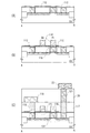
本実施の形態では、半導体メモリ装置の形状について図8を用いて説明する。図8(A)は、実施の形態3で示した半導体メモリ装置の単結晶シリコン基板上に設けられた主要な配線・電極等と同じものである。図5(A)は1つの記憶セルを中心に示したが、図8(A)では、さらに他の記憶セルとの関係がわかるように表示してある。図8(A)には、記憶セルの大きさを決定する上で重要な長さや間隔である、ゲート電極111間の間隔a、導電性領域106間の間隔b、ゲート電極111の長さcが示されている
本実施の形態では、別の半導体メモリ装置の形状について説明する。図9に本実施の形態の半導体メモリ装置の記憶ユニットのレイアウト例を示す。本実施の形態で示す半導体メモリ装置は、配線のパターン等は異なるが、実施の形態3で示した方法により作製できる。本実施の形態で示す半導体装置は、図4(A)で示される回路図に相当する回路配置を有する。
その結果、図5(A)あるいは図8(A)で示す構造の半導体メモリ装置に比べて、より高密度にゲート電極111を配置できる。図8(A)で示す構造の半導体メモリ装置では、ゲート電極111を同一直線上に配置したため、ゲート電極111間の間隔aを、最小加工線幅(F)とする必要があった。その結果、隣接する導電性領域106間の間隔bは最小加工線幅の2倍(2F)以上とする必要があった。
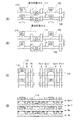
本実施の形態では、さらに異なる半導体メモリ装置の形状について説明する。本実施の形態では、図9(A)に示された導電性領域106の間隔b1とb2を異なる値とすることによる効果について説明する。図10に本実施の形態の半導体メモリ装置の記憶ユニットのレイアウト例を示す。本実施の形態で示す半導体メモリ装置は、配線のパターン等は異なるが、実施の形態3で示した方法により作製できる。本実施の形態で示す半導体装置は、図4(A)で示される回路図に相当する回路配置を有する。
本実施の形態では、図12(A)に示す半導体メモリ装置の動作の例について、図13を用いて説明する。なお、電位として、以下に具体的な数値を挙げるが、それは、本発明の技術思想の理解を助けることが目的である。言うまでもなく、それらの値はトランジスタやキャパシタのさまざまな特性によって、あるいは実施者の都合によって変更される。また、図12(A)に示される半導体メモリ装置は、以下の方法以外の方法によっても、データを書き込み、あるいは読み出すことができる。
本実施の形態では、図4(B)に示す半導体メモリ装置の動作の例について、図15および図16を用いて説明する。なお、電位として、以下に具体的な数値を挙げるが、それは、本発明の技術思想の理解を助けることが目的である。言うまでもなく、それらの値はトランジスタやキャパシタのさまざまな特性によって、あるいは実施者の都合によって変更される。また、図4(B)に示される半導体メモリ装置は、以下の方法以外の方法によっても、データを書き込み、あるいは読み出すことができる。
本実施の形態では、半導体メモリ装置の形状について説明する。図14に本実施の形態の半導体メモリ装置の記憶ユニットのレイアウト例を示す。本実施の形態で示す半導体装置は、図4(B)で示される回路図に相当する回路配置を有する。本実施の形態で示す半導体メモリ装置は、配線のパターン等は異なるが、実施の形態3で示した方法により作製できる。
本実施の形態では、実施の形態1乃至11に示した回路や半導体メモリ装置およびその駆動方法等を用いた電子機器について説明する。これらは、パーソナルコンピュータ、携帯通信機器、画像表示装置、映像再生装置、画像映像撮像装置、ゲーム機、電子書籍等の機器に用いることができる。
102 素子分離領域
103 ゲート絶縁膜
104 ダミーゲート
105 シリサイド領域
106 導電性領域
107 第1層間絶縁物
107a 第2層間絶縁物
108 第1開口部
109 第2開口部
110 第1接続電極
111 ゲート電極
112 酸化物半導体領域
113 ゲート絶縁膜
114 第1配線
115 n型の導電性を示す領域
116 キャパシタ
117 第3層間絶縁物
118 第2接続電極
119 第2配線
120 第4層間絶縁物
121 第3接続電極
122 第3配線
123 書き込みトランジスタ
124 読み出しトランジスタ
WTr 書き込みトランジスタ
RTr 読み出しトランジスタ
C キャパシタ
P 読み出しワード線
Q 書き込みワード線
R ビット線
S バイアス線
Claims (4)
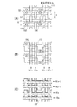
- 第1乃至第4の配線と、第1及び第2の記憶セルと、を有する半導体メモリ装置において、
前記第1および第2の配線は平行であり、
前記第3および第4の配線は平行であり、
前記第1の配線と前記第3の配線は交差し、
前記第1の記憶セルは、第1のトランジスタと、第2のトランジスタと、第1のキャパシタと、を有し、
前記第2の記憶セルは、第3のトランジスタと、第4のトランジスタと、第2のキャパシタと、を有し、
前記第1のトランジスタのドレインは、前記第2のトランジスタのゲートと電気的に接続され、
前記第1のトランジスタのドレインは、前記第1のキャパシタの一方の電極と電気的に接続され、
前記第3のトランジスタのドレインは、前記第4のトランジスタのゲートと電気的に接続され、
前記第3のトランジスタのドレインは、前記第2のキャパシタの一方の電極と電気的に接続され、
前記第1のトランジスタのゲートは、前記第2のキャパシタの他方の電極と電気的に接続され、
前記第1のトランジスタのゲートは、前記第1の配線と電気的に接続され、
前記第3のトランジスタのゲートは、前記第1のキャパシタの他方の電極と電気的に接続され、
前記第3のトランジスタのゲートは、前記第2の配線と電気的に接続され、
前記第1のトランジスタのソースは、前記第2のトランジスタのソースと電気的に接続され、
前記第1のトランジスタのソースは、前記第4のトランジスタのドレインと電気的に接続され、
前記第1のトランジスタのソースは、前記第3の配線と電気的に接続され、
前記第3のトランジスタのソースは、前記第4のトランジスタのソースと電気的に接続され、
前記第3のトランジスタのソースは、前記第2のトランジスタのドレインと電気的に接続され、
前記第3のトランジスタのソースは、前記第4の配線と電気的に接続され、
前記第1のトランジスタはバンドギャップが2.5電子ボルト以上の半導体よりなるチャネルを有することを特徴とする半導体メモリ装置。 - 第1乃至第5の配線と、第1乃至第4の記憶セルを有する半導体メモリ装置において、
前記第1および第2の配線は平行であり、
前記第3乃至第5の配線は平行であり、
前記第1の配線と前記第3の配線は交差し、
前記第1の記憶セルは、第1のトランジスタと、第2のトランジスタと、第1のキャパシタと、を有し、
前記第2の記憶セルは、第3のトランジスタと、第4のトランジスタと、第2のキャパシタと、を有し、
前記第3の記憶セルは、第5のトランジスタと、第6のトランジスタと、第3のキャパシタと、を有し、
前記第4の記憶セルは、第7のトランジスタと、第8のトランジスタと、第4のキャパシタと、を有し、
前記第1のトランジスタのドレインは、前記第2のトランジスタのゲートと電気的に接続され、
前記第1のトランジスタのドレインは、前記第1のキャパシタの一方の電極と電気的に接続され、
前記第3のトランジスタのドレインは、前記第4のトランジスタのゲートと電気的に接続され、
前記第3のトランジスタのドレインは、前記第2のキャパシタの一方の電極と電気的に接続され、
前記第5のトランジスタのドレインは、前記第6のトランジスタのゲートと電気的に接続され、
前記第5のトランジスタのドレインは、前記第3のキャパシタの一方の電極と電気的に接続され、
前記第7のトランジスタのドレインは、前記第8のトランジスタのゲートと電気的に接続され、
前記第7のトランジスタのドレインは、前記第4のキャパシタの一方の電極と電気的に接続され、
前記第1のトランジスタのゲートは、前記第2のキャパシタの他方の電極と電気的に接続され、
前記第1のトランジスタのゲートは、前記第5のトランジスタのゲートと電気的に接続され、
前記第1のトランジスタのゲートは、前記第4のキャパシタの他方の電極と電気的に接続され、
前記第1のトランジスタのゲートは、前記第1の配線と電気的に接続され、
前記第3のトランジスタのゲートは、前記第1のキャパシタの他方の電極と電気的に接続され、
前記第3のトランジスタのゲートは、前記第7のトランジスタのゲートと電気的に接続され、
前記第3のトランジスタのゲートは、前記第3のキャパシタの他方の電極と電気的に接続され、
前記第3のトランジスタのゲートは、前記第2の配線と電気的に接続され、
前記第1のトランジスタのソースは、前記第2のトランジスタのソースと電気的に接続され、
前記第1のトランジスタのソースは、前記第4のトランジスタのドレインと電気的に接続され、
前記第1のトランジスタのソースは、前記第3の配線と電気的に接続され、
前記第3のトランジスタのソースは、前記第4のトランジスタのソースと電気的に接続され、
前記第3のトランジスタのソースは、前記第2のトランジスタのドレインと電気的に接続され、
前記第3のトランジスタのソースは、前記第5のトランジスタのソースと電気的に接続され、
前記第3のトランジスタのソースは、前記第6のトランジスタのソースと電気的に接続され、
前記第3のトランジスタのソースは、前記第8のトランジスタのドレインと電気的に接続され、
前記第3のトランジスタのソースは、前記第4の配線と電気的に接続され、
前記第7のトランジスタのソースは、前記第8のトランジスタのソースと電気的に接続され、
前記第7のトランジスタのソースは、前記第6のトランジスタのドレインと電気的に接続され、
前記第7のトランジスタのソースは、前記第5の配線と電気的に接続され、
前記第1のトランジスタはバンドギャップが2.5電子ボルト以上の半導体よりなるチャネルを有することを特徴とする半導体メモリ装置。 - 請求項1または請求項2において、
前記第1のトランジスタの導電型がNチャネル型であることを特徴とする半導体メモリ装置。 - 請求項1乃至請求項3のいずれか一項において、
前記第2のトランジスタの導電型がPチャネル型であることを特徴とする半導体メモリ装置。
Priority Applications (1)
| Application Number | Priority Date | Filing Date | Title |
|---|---|---|---|
| JP2011097724A JP5651524B2 (ja) | 2010-04-27 | 2011-04-26 | 半導体メモリ装置 |
Applications Claiming Priority (5)
| Application Number | Priority Date | Filing Date | Title |
|---|---|---|---|
| JP2010101571 | 2010-04-27 | ||
| JP2010102329 | 2010-04-27 | ||
| JP2010101571 | 2010-04-27 | ||
| JP2010102329 | 2010-04-27 | ||
| JP2011097724A JP5651524B2 (ja) | 2010-04-27 | 2011-04-26 | 半導体メモリ装置 |
Publications (3)
| Publication Number | Publication Date |
|---|---|
| JP2011249782A JP2011249782A (ja) | 2011-12-08 |
| JP2011249782A5 JP2011249782A5 (ja) | 2014-04-17 |
| JP5651524B2 true JP5651524B2 (ja) | 2015-01-14 |
Family
ID=44815038
Family Applications (1)
| Application Number | Title | Priority Date | Filing Date |
|---|---|---|---|
| JP2011097724A Active JP5651524B2 (ja) | 2010-04-27 | 2011-04-26 | 半導体メモリ装置 |
Country Status (4)
| Country | Link |
|---|---|
| US (1) | US8605477B2 (ja) |
| JP (1) | JP5651524B2 (ja) |
| TW (1) | TWI509777B (ja) |
| WO (1) | WO2011135999A1 (ja) |
Cited By (1)
| Publication number | Priority date | Publication date | Assignee | Title |
|---|---|---|---|---|
| JP2017084440A (ja) * | 2010-11-08 | 2017-05-18 | 株式会社半導体エネルギー研究所 | 半導体メモリ装置 |
Families Citing this family (39)
| Publication number | Priority date | Publication date | Assignee | Title |
|---|---|---|---|---|
| KR101761432B1 (ko) | 2009-11-06 | 2017-07-25 | 가부시키가이샤 한도오따이 에네루기 켄큐쇼 | 반도체 장치 |
| KR101921618B1 (ko) * | 2010-02-05 | 2018-11-26 | 가부시키가이샤 한도오따이 에네루기 켄큐쇼 | 반도체 장치 및 반도체 장치의 구동 방법 |
| WO2011108475A1 (en) * | 2010-03-04 | 2011-09-09 | Semiconductor Energy Laboratory Co., Ltd. | Semiconductor memory device and semiconductor device |
| KR101884031B1 (ko) | 2010-04-07 | 2018-07-31 | 가부시키가이샤 한도오따이 에네루기 켄큐쇼 | 반도체 기억 장치 |
| US8416622B2 (en) | 2010-05-20 | 2013-04-09 | Semiconductor Energy Laboratory Co., Ltd. | Driving method of a semiconductor device with an inverted period having a negative potential applied to a gate of an oxide semiconductor transistor |
| US8582348B2 (en) | 2010-08-06 | 2013-11-12 | Semiconductor Energy Laboratory Co., Ltd. | Semiconductor device and method for driving semiconductor device |
| US8422272B2 (en) | 2010-08-06 | 2013-04-16 | Semiconductor Energy Laboratory Co., Ltd. | Semiconductor device and driving method thereof |
| TWI520273B (zh) | 2011-02-02 | 2016-02-01 | 半導體能源研究所股份有限公司 | 半導體儲存裝置 |
| WO2012153473A1 (en) | 2011-05-06 | 2012-11-15 | Semiconductor Energy Laboratory Co., Ltd. | Semiconductor device |
| US8837203B2 (en) * | 2011-05-19 | 2014-09-16 | Semiconductor Energy Laboratory Co., Ltd. | Semiconductor device |
| JP6013682B2 (ja) | 2011-05-20 | 2016-10-25 | 株式会社半導体エネルギー研究所 | 半導体装置の駆動方法 |
| US8569129B2 (en) | 2011-05-31 | 2013-10-29 | Taiwan Semiconductor Manufacturing Company, Ltd. | Device-manufacturing scheme for increasing the density of metal patterns in inter-layer dielectrics |
| US9001564B2 (en) | 2011-06-29 | 2015-04-07 | Semiconductor Energy Laboratory Co., Ltd. | Semiconductor device and a method for driving the same |
| US9490241B2 (en) * | 2011-07-08 | 2016-11-08 | Semiconductor Energy Laboratory Co., Ltd. | Semiconductor device comprising a first inverter and a second inverter |
| US8736315B2 (en) * | 2011-09-30 | 2014-05-27 | Semiconductor Energy Laboratory Co., Ltd. | Semiconductor device |
| JP6012450B2 (ja) * | 2011-12-23 | 2016-10-25 | 株式会社半導体エネルギー研究所 | 半導体装置の駆動方法 |
| US20130187150A1 (en) * | 2012-01-20 | 2013-07-25 | Semiconductor Energy Laboratory Co., Ltd. | Semiconductor device |
| JP5674832B2 (ja) * | 2012-01-25 | 2015-02-25 | 富士フイルム株式会社 | キャパシタ形成方法、半導体基板製品の製造方法、およびエッチング液 |
| US9312257B2 (en) | 2012-02-29 | 2016-04-12 | Semiconductor Energy Laboratory Co., Ltd. | Semiconductor device |
| US9054678B2 (en) * | 2012-07-06 | 2015-06-09 | Semiconductor Energy Laboratory Co., Ltd. | Semiconductor device and driving method thereof |
| JP6516978B2 (ja) * | 2013-07-17 | 2019-05-22 | 株式会社半導体エネルギー研究所 | 半導体装置 |
| JP6333580B2 (ja) * | 2014-03-07 | 2018-05-30 | 株式会社半導体エネルギー研究所 | 半導体装置 |
| US9716100B2 (en) * | 2014-03-14 | 2017-07-25 | Semiconductor Energy Laboratory Co., Ltd. | Semiconductor device, method for driving semiconductor device, and electronic device |
| US9887212B2 (en) * | 2014-03-14 | 2018-02-06 | Semiconductor Energy Laboratory Co., Ltd. | Semiconductor device and electronic device |
| KR102238689B1 (ko) * | 2014-03-14 | 2021-04-08 | 가부시키가이샤 한도오따이 에네루기 켄큐쇼 | 반도체 장치, 전자 부품, 및 전자 기기 |
| WO2015182000A1 (en) | 2014-05-30 | 2015-12-03 | Semiconductor Energy Laboratory Co., Ltd. | Semiconductor device, manufacturing method thereof, and electronic device |
| US9728721B2 (en) | 2014-07-25 | 2017-08-08 | Globalfoundries Singapore Pte. Ltd. | Resistive memory device |
| CN107167976A (zh) * | 2017-07-13 | 2017-09-15 | 京东方科技集团股份有限公司 | 一种像素电路、显示面板、显示装置及其驱动方法 |
| JP2019102110A (ja) * | 2017-11-30 | 2019-06-24 | 植 千葉 | 半導体メモリ |
| JP7186684B2 (ja) * | 2019-09-17 | 2022-12-09 | 株式会社東芝 | 半導体装置 |
| US11139006B1 (en) * | 2020-03-12 | 2021-10-05 | Ememory Technology Inc. | Self-biased sense amplification circuit |
| DE102020133486A1 (de) * | 2020-05-28 | 2021-12-02 | Taiwan Semiconductor Manufacturing Co. Ltd. | Nichtflüchtiger speicher mit doppelter ansteuerung |
| US11716862B2 (en) * | 2020-05-28 | 2023-08-01 | Taiwan Semiconductor Manufacturing Company, Ltd. | Non-volatile memory with dual gated control |
| US11380695B2 (en) * | 2020-10-30 | 2022-07-05 | Ferroelectric Memory Gmbh | Memory cell arrangement and method thereof |
| US11335391B1 (en) | 2020-10-30 | 2022-05-17 | Ferroelectric Memory Gmbh | Memory cell arrangement and method thereof |
| US11527551B2 (en) | 2020-10-30 | 2022-12-13 | Ferroelectric Memory Gmbh | Memory cell arrangements and methods thereof |
| CN113257300B (zh) * | 2021-06-03 | 2023-06-06 | 清华大学 | 基于铁电电容的存储装置 |
| CN116234308B (zh) * | 2022-07-07 | 2024-02-20 | 北京超弦存储器研究院 | 存储单元、存储器及其控制方法、电子设备 |
| CN116209247B (zh) * | 2022-08-08 | 2024-02-20 | 北京超弦存储器研究院 | 动态存储器、其制作方法、读取方法及存储装置 |
Family Cites Families (110)
| Publication number | Priority date | Publication date | Assignee | Title |
|---|---|---|---|---|
| US8021A (en) * | 1851-04-01 | Brick-press | ||
| DE3171836D1 (en) | 1980-12-08 | 1985-09-19 | Toshiba Kk | Semiconductor memory device |
| KR100394896B1 (ko) | 1995-08-03 | 2003-11-28 | 코닌클리케 필립스 일렉트로닉스 엔.브이. | 투명스위칭소자를포함하는반도체장치 |
| JP3625598B2 (ja) | 1995-12-30 | 2005-03-02 | 三星電子株式会社 | 液晶表示装置の製造方法 |
| JP4103968B2 (ja) | 1996-09-18 | 2008-06-18 | 株式会社半導体エネルギー研究所 | 絶縁ゲイト型半導体装置 |
| JP4170454B2 (ja) | 1998-07-24 | 2008-10-22 | Hoya株式会社 | 透明導電性酸化物薄膜を有する物品及びその製造方法 |
| JP2000150861A (ja) | 1998-11-16 | 2000-05-30 | Tdk Corp | 酸化物薄膜 |
| JP3276930B2 (ja) | 1998-11-17 | 2002-04-22 | 科学技術振興事業団 | トランジスタ及び半導体装置 |
| JP2001053164A (ja) * | 1999-08-04 | 2001-02-23 | Sony Corp | 半導体記憶装置 |
| TW460731B (en) | 1999-09-03 | 2001-10-21 | Ind Tech Res Inst | Electrode structure and production method of wide viewing angle LCD |
| JP4089858B2 (ja) | 2000-09-01 | 2008-05-28 | 国立大学法人東北大学 | 半導体デバイス |
| JP2002093178A (ja) * | 2000-09-13 | 2002-03-29 | Sony Corp | 半導体記憶装置および動作方法 |
| KR20020038482A (ko) | 2000-11-15 | 2002-05-23 | 모리시타 요이찌 | 박막 트랜지스터 어레이, 그 제조방법 및 그것을 이용한표시패널 |
| JP3997731B2 (ja) | 2001-03-19 | 2007-10-24 | 富士ゼロックス株式会社 | 基材上に結晶性半導体薄膜を形成する方法 |
| JP2002289859A (ja) | 2001-03-23 | 2002-10-04 | Minolta Co Ltd | 薄膜トランジスタ |
| JP3925839B2 (ja) | 2001-09-10 | 2007-06-06 | シャープ株式会社 | 半導体記憶装置およびその試験方法 |
| JP4090716B2 (ja) | 2001-09-10 | 2008-05-28 | 雅司 川崎 | 薄膜トランジスタおよびマトリクス表示装置 |
| EP1443130B1 (en) | 2001-11-05 | 2011-09-28 | Japan Science and Technology Agency | Natural superlattice homologous single crystal thin film, method for preparation thereof, and device using said single crystal thin film |
| JP4164562B2 (ja) | 2002-09-11 | 2008-10-15 | 独立行政法人科学技術振興機構 | ホモロガス薄膜を活性層として用いる透明薄膜電界効果型トランジスタ |
| JP4083486B2 (ja) | 2002-02-21 | 2008-04-30 | 独立行政法人科学技術振興機構 | LnCuO(S,Se,Te)単結晶薄膜の製造方法 |
| CN1445821A (zh) | 2002-03-15 | 2003-10-01 | 三洋电机株式会社 | ZnO膜和ZnO半导体层的形成方法、半导体元件及其制造方法 |
| JP3933591B2 (ja) | 2002-03-26 | 2007-06-20 | 淳二 城戸 | 有機エレクトロルミネッセント素子 |
| US7339187B2 (en) | 2002-05-21 | 2008-03-04 | State Of Oregon Acting By And Through The Oregon State Board Of Higher Education On Behalf Of Oregon State University | Transistor structures |
| JP2004022625A (ja) | 2002-06-13 | 2004-01-22 | Murata Mfg Co Ltd | 半導体デバイス及び該半導体デバイスの製造方法 |
| US7105868B2 (en) | 2002-06-24 | 2006-09-12 | Cermet, Inc. | High-electron mobility transistor with zinc oxide |
| US7067843B2 (en) | 2002-10-11 | 2006-06-27 | E. I. Du Pont De Nemours And Company | Transparent oxide semiconductor thin film transistors |
| JP4166105B2 (ja) | 2003-03-06 | 2008-10-15 | シャープ株式会社 | 半導体装置およびその製造方法 |
| JP2004273732A (ja) | 2003-03-07 | 2004-09-30 | Sharp Corp | アクティブマトリクス基板およびその製造方法 |
| JP4108633B2 (ja) | 2003-06-20 | 2008-06-25 | シャープ株式会社 | 薄膜トランジスタおよびその製造方法ならびに電子デバイス |
| US7262463B2 (en) | 2003-07-25 | 2007-08-28 | Hewlett-Packard Development Company, L.P. | Transistor including a deposited channel region having a doped portion |
| US7145174B2 (en) | 2004-03-12 | 2006-12-05 | Hewlett-Packard Development Company, Lp. | Semiconductor device |
| EP2413366B1 (en) | 2004-03-12 | 2017-01-11 | Japan Science And Technology Agency | A switching element of LCDs or organic EL displays |
| US7282782B2 (en) | 2004-03-12 | 2007-10-16 | Hewlett-Packard Development Company, L.P. | Combined binary oxide semiconductor device |
| US7297977B2 (en) | 2004-03-12 | 2007-11-20 | Hewlett-Packard Development Company, L.P. | Semiconductor device |
| JP2005340356A (ja) * | 2004-05-25 | 2005-12-08 | Hitachi Ltd | 半導体記憶装置 |
| US7211825B2 (en) | 2004-06-14 | 2007-05-01 | Yi-Chi Shih | Indium oxide-based thin film transistors and circuits |
| JP2006100760A (ja) | 2004-09-02 | 2006-04-13 | Casio Comput Co Ltd | 薄膜トランジスタおよびその製造方法 |
| US7285501B2 (en) | 2004-09-17 | 2007-10-23 | Hewlett-Packard Development Company, L.P. | Method of forming a solution processed device |
| JP2006121029A (ja) * | 2004-09-27 | 2006-05-11 | Tokyo Institute Of Technology | 固体電子装置 |
| US7298084B2 (en) | 2004-11-02 | 2007-11-20 | 3M Innovative Properties Company | Methods and displays utilizing integrated zinc oxide row and column drivers in conjunction with organic light emitting diodes |
| US7791072B2 (en) | 2004-11-10 | 2010-09-07 | Canon Kabushiki Kaisha | Display |
| US7453065B2 (en) | 2004-11-10 | 2008-11-18 | Canon Kabushiki Kaisha | Sensor and image pickup device |
| CN101057339B (zh) | 2004-11-10 | 2012-12-26 | 佳能株式会社 | 无定形氧化物和场效应晶体管 |
| US7863611B2 (en) | 2004-11-10 | 2011-01-04 | Canon Kabushiki Kaisha | Integrated circuits utilizing amorphous oxides |
| KR100953596B1 (ko) | 2004-11-10 | 2010-04-21 | 캐논 가부시끼가이샤 | 발광장치 |
| CN101057338B (zh) | 2004-11-10 | 2011-03-16 | 佳能株式会社 | 采用无定形氧化物的场效应晶体管 |
| US7829444B2 (en) | 2004-11-10 | 2010-11-09 | Canon Kabushiki Kaisha | Field effect transistor manufacturing method |
| US7579224B2 (en) | 2005-01-21 | 2009-08-25 | Semiconductor Energy Laboratory Co., Ltd. | Method for manufacturing a thin film semiconductor device |
| TWI472037B (zh) | 2005-01-28 | 2015-02-01 | Semiconductor Energy Lab | 半導體裝置,電子裝置,和半導體裝置的製造方法 |
| TWI569441B (zh) | 2005-01-28 | 2017-02-01 | 半導體能源研究所股份有限公司 | 半導體裝置,電子裝置,和半導體裝置的製造方法 |
| US7858451B2 (en) | 2005-02-03 | 2010-12-28 | Semiconductor Energy Laboratory Co., Ltd. | Electronic device, semiconductor device and manufacturing method thereof |
| US7948171B2 (en) | 2005-02-18 | 2011-05-24 | Semiconductor Energy Laboratory Co., Ltd. | Light emitting device |
| US20060197092A1 (en) | 2005-03-03 | 2006-09-07 | Randy Hoffman | System and method for forming conductive material on a substrate |
| US8681077B2 (en) | 2005-03-18 | 2014-03-25 | Semiconductor Energy Laboratory Co., Ltd. | Semiconductor device, and display device, driving method and electronic apparatus thereof |
| WO2006105077A2 (en) | 2005-03-28 | 2006-10-05 | Massachusetts Institute Of Technology | Low voltage thin film transistor with high-k dielectric material |
| US7645478B2 (en) | 2005-03-31 | 2010-01-12 | 3M Innovative Properties Company | Methods of making displays |
| JP4849817B2 (ja) | 2005-04-08 | 2012-01-11 | ルネサスエレクトロニクス株式会社 | 半導体記憶装置 |
| US8300031B2 (en) | 2005-04-20 | 2012-10-30 | Semiconductor Energy Laboratory Co., Ltd. | Semiconductor device comprising transistor having gate and drain connected through a current-voltage conversion element |
| JP2006338730A (ja) * | 2005-05-31 | 2006-12-14 | Sony Corp | 半導体記憶装置 |
| JP2006344849A (ja) | 2005-06-10 | 2006-12-21 | Casio Comput Co Ltd | 薄膜トランジスタ |
| US7402506B2 (en) | 2005-06-16 | 2008-07-22 | Eastman Kodak Company | Methods of making thin film transistors comprising zinc-oxide-based semiconductor materials and transistors made thereby |
| US7691666B2 (en) | 2005-06-16 | 2010-04-06 | Eastman Kodak Company | Methods of making thin film transistors comprising zinc-oxide-based semiconductor materials and transistors made thereby |
| US7507618B2 (en) | 2005-06-27 | 2009-03-24 | 3M Innovative Properties Company | Method for making electronic devices using metal oxide nanoparticles |
| KR100711890B1 (ko) | 2005-07-28 | 2007-04-25 | 삼성에스디아이 주식회사 | 유기 발광표시장치 및 그의 제조방법 |
| JP2007042172A (ja) * | 2005-08-01 | 2007-02-15 | Sony Corp | 半導体メモリ装置 |
| JP2007059128A (ja) | 2005-08-23 | 2007-03-08 | Canon Inc | 有機el表示装置およびその製造方法 |
| JP2007073705A (ja) | 2005-09-06 | 2007-03-22 | Canon Inc | 酸化物半導体チャネル薄膜トランジスタおよびその製造方法 |
| JP4280736B2 (ja) | 2005-09-06 | 2009-06-17 | キヤノン株式会社 | 半導体素子 |
| JP4850457B2 (ja) | 2005-09-06 | 2012-01-11 | キヤノン株式会社 | 薄膜トランジスタ及び薄膜ダイオード |
| JP5116225B2 (ja) | 2005-09-06 | 2013-01-09 | キヤノン株式会社 | 酸化物半導体デバイスの製造方法 |
| EP3614442A3 (en) | 2005-09-29 | 2020-03-25 | Semiconductor Energy Laboratory Co., Ltd. | Semiconductor device having oxide semiconductor layer and manufactoring method thereof |
| JP5037808B2 (ja) | 2005-10-20 | 2012-10-03 | キヤノン株式会社 | アモルファス酸化物を用いた電界効果型トランジスタ、及び該トランジスタを用いた表示装置 |
| KR20090115222A (ko) | 2005-11-15 | 2009-11-04 | 가부시키가이샤 한도오따이 에네루기 켄큐쇼 | 반도체장치 제조방법 |
| TWI292281B (en) | 2005-12-29 | 2008-01-01 | Ind Tech Res Inst | Pixel structure of active organic light emitting diode and method of fabricating the same |
| US7867636B2 (en) | 2006-01-11 | 2011-01-11 | Murata Manufacturing Co., Ltd. | Transparent conductive film and method for manufacturing the same |
| JP4977478B2 (ja) | 2006-01-21 | 2012-07-18 | 三星電子株式会社 | ZnOフィルム及びこれを用いたTFTの製造方法 |
| US7576394B2 (en) | 2006-02-02 | 2009-08-18 | Kochi Industrial Promotion Center | Thin film transistor including low resistance conductive thin films and manufacturing method thereof |
| US7977169B2 (en) | 2006-02-15 | 2011-07-12 | Kochi Industrial Promotion Center | Semiconductor device including active layer made of zinc oxide with controlled orientations and manufacturing method thereof |
| KR20070101595A (ko) | 2006-04-11 | 2007-10-17 | 삼성전자주식회사 | ZnO TFT |
| US20070252928A1 (en) | 2006-04-28 | 2007-11-01 | Toppan Printing Co., Ltd. | Structure, transmission type liquid crystal display, reflection type display and manufacturing method thereof |
| JP5028033B2 (ja) | 2006-06-13 | 2012-09-19 | キヤノン株式会社 | 酸化物半導体膜のドライエッチング方法 |
| JP4609797B2 (ja) | 2006-08-09 | 2011-01-12 | Nec液晶テクノロジー株式会社 | 薄膜デバイス及びその製造方法 |
| JP4999400B2 (ja) | 2006-08-09 | 2012-08-15 | キヤノン株式会社 | 酸化物半導体膜のドライエッチング方法 |
| JP4332545B2 (ja) | 2006-09-15 | 2009-09-16 | キヤノン株式会社 | 電界効果型トランジスタ及びその製造方法 |
| JP4274219B2 (ja) | 2006-09-27 | 2009-06-03 | セイコーエプソン株式会社 | 電子デバイス、有機エレクトロルミネッセンス装置、有機薄膜半導体装置 |
| JP5164357B2 (ja) | 2006-09-27 | 2013-03-21 | キヤノン株式会社 | 半導体装置及び半導体装置の製造方法 |
| US7622371B2 (en) | 2006-10-10 | 2009-11-24 | Hewlett-Packard Development Company, L.P. | Fused nanocrystal thin film semiconductor and method |
| US7772021B2 (en) | 2006-11-29 | 2010-08-10 | Samsung Electronics Co., Ltd. | Flat panel displays comprising a thin-film transistor having a semiconductive oxide in its channel and methods of fabricating the same for use in flat panel displays |
| JP2008140684A (ja) | 2006-12-04 | 2008-06-19 | Toppan Printing Co Ltd | カラーelディスプレイおよびその製造方法 |
| KR101303578B1 (ko) | 2007-01-05 | 2013-09-09 | 삼성전자주식회사 | 박막 식각 방법 |
| US8207063B2 (en) | 2007-01-26 | 2012-06-26 | Eastman Kodak Company | Process for atomic layer deposition |
| US7994000B2 (en) | 2007-02-27 | 2011-08-09 | Semiconductor Energy Laboratory Co., Ltd. | Semiconductor device and method of manufacturing the same |
| KR100851215B1 (ko) | 2007-03-14 | 2008-08-07 | 삼성에스디아이 주식회사 | 박막 트랜지스터 및 이를 이용한 유기 전계 발광표시장치 |
| US7795613B2 (en) | 2007-04-17 | 2010-09-14 | Toppan Printing Co., Ltd. | Structure with transistor |
| KR101325053B1 (ko) | 2007-04-18 | 2013-11-05 | 삼성디스플레이 주식회사 | 박막 트랜지스터 기판 및 이의 제조 방법 |
| KR20080094300A (ko) | 2007-04-19 | 2008-10-23 | 삼성전자주식회사 | 박막 트랜지스터 및 그 제조 방법과 박막 트랜지스터를포함하는 평판 디스플레이 |
| KR101334181B1 (ko) | 2007-04-20 | 2013-11-28 | 삼성전자주식회사 | 선택적으로 결정화된 채널층을 갖는 박막 트랜지스터 및 그제조 방법 |
| JP2008269751A (ja) * | 2007-04-25 | 2008-11-06 | Semiconductor Energy Lab Co Ltd | 半導体記憶装置及び当該半導体記憶装置を具備する電子機器 |
| CN101663762B (zh) | 2007-04-25 | 2011-09-21 | 佳能株式会社 | 氧氮化物半导体 |
| KR101345376B1 (ko) | 2007-05-29 | 2013-12-24 | 삼성전자주식회사 | ZnO 계 박막 트랜지스터 및 그 제조방법 |
| JP5215158B2 (ja) | 2007-12-17 | 2013-06-19 | 富士フイルム株式会社 | 無機結晶性配向膜及びその製造方法、半導体デバイス |
| JP4623179B2 (ja) | 2008-09-18 | 2011-02-02 | ソニー株式会社 | 薄膜トランジスタおよびその製造方法 |
| JP5451280B2 (ja) | 2008-10-09 | 2014-03-26 | キヤノン株式会社 | ウルツ鉱型結晶成長用基板およびその製造方法ならびに半導体装置 |
| JP5781720B2 (ja) | 2008-12-15 | 2015-09-24 | ルネサスエレクトロニクス株式会社 | 半導体装置及び半導体装置の製造方法 |
| CN105702631B (zh) | 2009-12-28 | 2019-05-28 | 株式会社半导体能源研究所 | 半导体器件 |
| KR101842413B1 (ko) | 2009-12-28 | 2018-03-26 | 가부시키가이샤 한도오따이 에네루기 켄큐쇼 | 반도체 장치 |
| KR101848516B1 (ko) | 2010-01-15 | 2018-04-12 | 가부시키가이샤 한도오따이 에네루기 켄큐쇼 | 반도체 장치 |
| CN102725842B (zh) | 2010-02-05 | 2014-12-03 | 株式会社半导体能源研究所 | 半导体器件 |
| WO2011105310A1 (en) | 2010-02-26 | 2011-09-01 | Semiconductor Energy Laboratory Co., Ltd. | Semiconductor device |
| KR101884031B1 (ko) | 2010-04-07 | 2018-07-31 | 가부시키가이샤 한도오따이 에네루기 켄큐쇼 | 반도체 기억 장치 |
-
2011
- 2011-04-01 WO PCT/JP2011/058860 patent/WO2011135999A1/en active Application Filing
- 2011-04-20 TW TW100113719A patent/TWI509777B/zh not_active IP Right Cessation
- 2011-04-25 US US13/093,018 patent/US8605477B2/en not_active Expired - Fee Related
- 2011-04-26 JP JP2011097724A patent/JP5651524B2/ja active Active
Cited By (1)
| Publication number | Priority date | Publication date | Assignee | Title |
|---|---|---|---|---|
| JP2017084440A (ja) * | 2010-11-08 | 2017-05-18 | 株式会社半導体エネルギー研究所 | 半導体メモリ装置 |
Also Published As
| Publication number | Publication date |
|---|---|
| US8605477B2 (en) | 2013-12-10 |
| WO2011135999A1 (en) | 2011-11-03 |
| JP2011249782A (ja) | 2011-12-08 |
| TWI509777B (zh) | 2015-11-21 |
| TW201214675A (en) | 2012-04-01 |
| US20110260158A1 (en) | 2011-10-27 |
Similar Documents
| Publication | Publication Date | Title |
|---|---|---|
| JP5651524B2 (ja) | 半導体メモリ装置 | |
| JP5865421B2 (ja) | 半導体装置 | |
| JP6480043B2 (ja) | 半導体装置 | |
| JP6174230B2 (ja) | 半導体メモリ装置 | |
| JP5813840B2 (ja) | 半導体装置 | |
| JP5823707B2 (ja) | 半導体装置 | |
| KR101889285B1 (ko) | 반도체 메모리 장치, 그 구동 방법, 및 반도체 장치 제작 방법 |
Legal Events
| Date | Code | Title | Description |
|---|---|---|---|
| A521 | Request for written amendment filed |
Free format text: JAPANESE INTERMEDIATE CODE: A523 Effective date: 20140228 |
|
| A621 | Written request for application examination |
Free format text: JAPANESE INTERMEDIATE CODE: A621 Effective date: 20140228 |
|
| A977 | Report on retrieval |
Free format text: JAPANESE INTERMEDIATE CODE: A971007 Effective date: 20140829 |
|
| A131 | Notification of reasons for refusal |
Free format text: JAPANESE INTERMEDIATE CODE: A131 Effective date: 20140916 |
|
| A521 | Request for written amendment filed |
Free format text: JAPANESE INTERMEDIATE CODE: A523 Effective date: 20140919 |
|
| TRDD | Decision of grant or rejection written | ||
| A01 | Written decision to grant a patent or to grant a registration (utility model) |
Free format text: JAPANESE INTERMEDIATE CODE: A01 Effective date: 20141111 |
|
| A61 | First payment of annual fees (during grant procedure) |
Free format text: JAPANESE INTERMEDIATE CODE: A61 Effective date: 20141117 |
|
| R150 | Certificate of patent or registration of utility model |
Ref document number: 5651524 Country of ref document: JP Free format text: JAPANESE INTERMEDIATE CODE: R150 |
|
| R250 | Receipt of annual fees |
Free format text: JAPANESE INTERMEDIATE CODE: R250 |
|
| R250 | Receipt of annual fees |
Free format text: JAPANESE INTERMEDIATE CODE: R250 |
|
| R250 | Receipt of annual fees |
Free format text: JAPANESE INTERMEDIATE CODE: R250 |
|
| R250 | Receipt of annual fees |
Free format text: JAPANESE INTERMEDIATE CODE: R250 |
|
| R250 | Receipt of annual fees |
Free format text: JAPANESE INTERMEDIATE CODE: R250 |
|
| R250 | Receipt of annual fees |
Free format text: JAPANESE INTERMEDIATE CODE: R250 |