JP5643268B2 - Light emitting diode driving circuit, light emitting diode driving device and driving method - Google Patents
Light emitting diode driving circuit, light emitting diode driving device and driving method Download PDFInfo
- Publication number
- JP5643268B2 JP5643268B2 JP2012196985A JP2012196985A JP5643268B2 JP 5643268 B2 JP5643268 B2 JP 5643268B2 JP 2012196985 A JP2012196985 A JP 2012196985A JP 2012196985 A JP2012196985 A JP 2012196985A JP 5643268 B2 JP5643268 B2 JP 5643268B2
- Authority
- JP
- Japan
- Prior art keywords
- signal
- light emitting
- emitting diode
- clock signal
- unit
- Prior art date
- Legal status (The legal status is an assumption and is not a legal conclusion. Google has not performed a legal analysis and makes no representation as to the accuracy of the status listed.)
- Expired - Fee Related
Links
Images


Classifications
-
- H—ELECTRICITY
- H05—ELECTRIC TECHNIQUES NOT OTHERWISE PROVIDED FOR
- H05B—ELECTRIC HEATING; ELECTRIC LIGHT SOURCES NOT OTHERWISE PROVIDED FOR; CIRCUIT ARRANGEMENTS FOR ELECTRIC LIGHT SOURCES, IN GENERAL
- H05B47/00—Circuit arrangements for operating light sources in general, i.e. where the type of light source is not relevant
- H05B47/10—Controlling the light source
- H05B47/175—Controlling the light source by remote control
- H05B47/185—Controlling the light source by remote control via power line carrier transmission
-
- H—ELECTRICITY
- H05—ELECTRIC TECHNIQUES NOT OTHERWISE PROVIDED FOR
- H05B—ELECTRIC HEATING; ELECTRIC LIGHT SOURCES NOT OTHERWISE PROVIDED FOR; CIRCUIT ARRANGEMENTS FOR ELECTRIC LIGHT SOURCES, IN GENERAL
- H05B45/00—Circuit arrangements for operating light-emitting diodes [LED]
- H05B45/30—Driver circuits
-
- G—PHYSICS
- G09—EDUCATION; CRYPTOGRAPHY; DISPLAY; ADVERTISING; SEALS
- G09G—ARRANGEMENTS OR CIRCUITS FOR CONTROL OF INDICATING DEVICES USING STATIC MEANS TO PRESENT VARIABLE INFORMATION
- G09G2310/00—Command of the display device
- G09G2310/02—Addressing, scanning or driving the display screen or processing steps related thereto
- G09G2310/0264—Details of driving circuits
- G09G2310/0267—Details of drivers for scan electrodes, other than drivers for liquid crystal, plasma or OLED displays
-
- G—PHYSICS
- G09—EDUCATION; CRYPTOGRAPHY; DISPLAY; ADVERTISING; SEALS
- G09G—ARRANGEMENTS OR CIRCUITS FOR CONTROL OF INDICATING DEVICES USING STATIC MEANS TO PRESENT VARIABLE INFORMATION
- G09G3/00—Control arrangements or circuits, of interest only in connection with visual indicators other than cathode-ray tubes
- G09G3/20—Control arrangements or circuits, of interest only in connection with visual indicators other than cathode-ray tubes for presentation of an assembly of a number of characters, e.g. a page, by composing the assembly by combination of individual elements arranged in a matrix no fixed position being assigned to or needed to be assigned to the individual characters or partial characters
- G09G3/34—Control arrangements or circuits, of interest only in connection with visual indicators other than cathode-ray tubes for presentation of an assembly of a number of characters, e.g. a page, by composing the assembly by combination of individual elements arranged in a matrix no fixed position being assigned to or needed to be assigned to the individual characters or partial characters by control of light from an independent source
- G09G3/36—Control arrangements or circuits, of interest only in connection with visual indicators other than cathode-ray tubes for presentation of an assembly of a number of characters, e.g. a page, by composing the assembly by combination of individual elements arranged in a matrix no fixed position being assigned to or needed to be assigned to the individual characters or partial characters by control of light from an independent source using liquid crystals
- G09G3/3611—Control of matrices with row and column drivers
- G09G3/3648—Control of matrices with row and column drivers using an active matrix
- G09G3/3655—Details of drivers for counter electrodes, e.g. common electrodes for pixel capacitors or supplementary storage capacitors
Description
本発明は発光ダイオード駆動回路、発光ダイオード駆動装置および駆動方法に関する。 The present invention relates to a light emitting diode driving circuit, a light emitting diode driving device, and a driving method.
発光ダイオード(Light Emitting Diode、LED)は高い光電変換効率を有するとともに、操作安定性が高いうえパルス幅変調(Pulse Width Modulation、パルス幅変調)によって輝度を制御(またはグレイスケール制御ともいう)することができるため、例えば表示装置のバックライト、照明装置、広告ディスプレイまたは大型表示装置の画素単位といった数多くの電子装置の光源またはディスプレイデバイスなどに応用されている。(例えば、特許文献1参照) Light emitting diodes (LEDs) have high photoelectric conversion efficiency, high operational stability, and brightness control (also referred to as gray scale control) by pulse width modulation (pulse width modulation). Therefore, it is applied to a light source or a display device of many electronic devices such as a backlight of a display device, a lighting device, an advertisement display or a pixel unit of a large display device. (For example, see Patent Document 1)
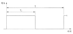
従来の発光ダイオード駆動回路1である図1Aを参照されたい。発光ダイオード駆動回路1はデータレジスタユニット11と、カウンタ12と、コンパレータ13と、ドライバ14とを有している。データレジスタユニット11はシステム側(図示されていない)からのグレイスケール情報を受信して保存している。カウンタ12はシステム側が出力したクロック信号を受信する。コンパレータ13の第一端131はデータレジスタユニット11に接続されており、コンパレータ13の第二端132はカウンタ12に接続されるとともに第一端131および第二端132はそれぞれデータレジスタユニット11およびカウンタ12が出力した信号を受信している。コンパレータ13は第一端131および第二端132が受信した信号を比較し、第一端131が受信した信号が第二端132が受信した信号よりも大きい場合、コンパレータ13の出力端に論理的な高電位が発生することで、ドライバ14が定電流源(Constant Current Source)によって発光ダイオードを点灯させている。第二端132が受信した信号が第一端131が受信した信号よりも大きい場合、コンパレータ13の出力端に論理的な低電位が発生すると同時に、ドライバ14は発光ダイオードを点灯させない。したがって、図1Bに示すように、コンパレータ13での比較結果により、ドライバ14はパルス幅変調信号を出力して、発光ダイオードに異なるグレイスケール(grayscale)の輝度を生じさせるものであり、かつ前記したパルス幅変調信号の動作周期T中における導通期間T1は、連続した導通期間である。このうち、グレイスケールは輝度の明暗レベルであり、従来の発光ダイオード駆動回路1ではドライバ14が出力したパルス幅変調信号により、発光ダイオードを異なる輝度で発光させている。導通期間T1が長いほど、発光ダイオードが点灯される期間は長く、輝度は高くなり、反対に、導通期間T1が短いほど、輝度は低くなり、導通期間T1がゼロのときには、発光ダイオードは消灯することを意味している。
Please refer to FIG. 1A which is a conventional
しかしながら、従来の発光ダイオード駆動回路1におけるコンパレータ13はデータレジスタユニット11およびカウンタ12からの信号を比較するために、大量の金属酸化膜半導体電界効果トランジスタ(MOSFET)から構成されており、例えばコンパレータ13にて12ビット(bit)のコンパレータを一つ使用する場合には、コンパレータ13内には少なくとも864個のMOSFETを有することになる。MOSFETはそれ自体がドレイン電流および寄生キャパシタンスという欠陥が存在しているので、大量のMOSFETを使用したコンパレータ13では予想外の電力が損失してしまうという問題があった。
However, the
したがって、不要な電力損失を減らすとともに、処理効率を高めることができる発光ダイオード駆動回路、発光ダイオード駆動装置および駆動方法を如何に提供するかということは、重要な課題の一つとなっていた。 Therefore, how to provide a light emitting diode driving circuit, a light emitting diode driving device, and a driving method capable of reducing unnecessary power loss and improving processing efficiency has been one of important issues.
上記課題に鑑み、本発明の目的は、不要な電力損失を減らすとともに、処理効率を高めることができる発光ダイオード駆動回路、発光ダイオード駆動装置および駆動方法を提供することにある。 In view of the above problems, an object of the present invention is to provide a light emitting diode driving circuit, a light emitting diode driving device, and a driving method capable of reducing unnecessary power loss and improving processing efficiency.
上記目的を達成するために、本発明に係る発光ダイオード駆動回路は発光ダイオードモジュールと組み合わされる。発光ダイオード駆動回路は読取りアドレス生成ユニットと、メモリユニットと、駆動ユニットとを包括している。読取りアドレス生成ユニットはクロック信号を受信するとともに読取り信号を出力する。メモリユニットは読取りアドレス生成ユニットに接続されるとともに、読取り信号に基づいて出力信号を生成する。駆動ユニットはメモリユニットに接続されるとともに、出力信号およびクロック信号を受信して、発光ダイオードモジュールに駆動信号を出力する。駆動ユニットはフリップフロップと、ドライバとを包括している。フリップフロップはメモリユニットに接続されるとともに、出力信号およびクロック信号を受信する。ドライバはフリップフロップに接続されるとともに駆動信号を出力する。クロック信号は二進重み付けクロック信号である。 In order to achieve the above object, a light emitting diode driving circuit according to the present invention is combined with a light emitting diode module. The LED driving circuit includes a read address generation unit, a memory unit, and a driving unit. The read address generation unit receives the clock signal and outputs a read signal. The memory unit is connected to the read address generation unit and generates an output signal based on the read signal. The drive unit is connected to the memory unit, receives an output signal and a clock signal, and outputs a drive signal to the light emitting diode module. The drive unit includes a flip-flop and a driver. The flip-flop is connected to the memory unit and receives an output signal and a clock signal. The driver is connected to the flip-flop and outputs a drive signal. The clock signal is a binary weighted clock signal.
本発明の一実施例において、読取りアドレス生成ユニットは読取りアドレスカウンタと、読取りアドレスデコーダとを包括している。読取りアドレスカウンタはクロック信号を受信する。読取りアドレスデコーダは読取りアドレスカウンタに接続されるとともに、読取り信号を出力する。 In one embodiment of the present invention, the read address generation unit includes a read address counter and a read address decoder. The read address counter receives a clock signal. The read address decoder is connected to a read address counter and outputs a read signal.
本発明の一実施例において、駆動信号は一動作周期中に複数の導通期間を有するとともに、これら導通期間は非連続である。 In one embodiment of the present invention, the drive signal has a plurality of conduction periods in one operation cycle, and these conduction periods are discontinuous.
本発明の一実施例において、メモリユニットはデュアルポートSRAMである。 In one embodiment of the present invention, the memory unit is a dual port SRAM.
本発明の一実施例において、発光ダイオード駆動回路は書込みアドレス生成ユニットと、シフトレジスタとをさらに包括している。書込みアドレス生成ユニットはメモリユニットに接続されるとともに、ラッチイネーブル信号に基づいてメモリユニットに書込み信号を出力する。シフトレジスタはメモリユニットに接続されている。 In one embodiment of the present invention, the light emitting diode driving circuit further includes a write address generation unit and a shift register. The write address generation unit is connected to the memory unit and outputs a write signal to the memory unit based on the latch enable signal. The shift register is connected to the memory unit.
本発明の一実施例において、書込みアドレス生成ユニットは書込みアドレスカウンタと、書込みアドレスデコーダとを包括している。書込みアドレスカウンタはラッチイネーブル信号を受信する。書込みアドレスデコーダは書込みアドレスカウンタに接続されるとともに、書込み信号を出力する。 In one embodiment of the present invention, the write address generation unit includes a write address counter and a write address decoder. The write address counter receives the latch enable signal. The write address decoder is connected to the write address counter and outputs a write signal.
上記目的を達成するために、本発明に係る発光ダイオードモジュールの駆動方法は発光ダイオード駆動回路と組み合わされ、発光ダイオード駆動回路は読取りアドレス生成ユニットと、メモリユニットと、駆動ユニットとを有している。駆動方法は、読取りアドレス生成ユニットがクロック信号を受信するとともに、メモリユニットに読取り信号を出力する工程と、メモリユニットが読取り信号に基づいて、出力信号を生成する工程と、駆動ユニットが出力信号およびクロック信号を受信するとともに、発光ダイオードモジュールに駆動信号を出力する工程と、を含む。駆動方法は、書込みアドレス生成ユニットによりラッチイネーブル信号に基づいてメモリユニットに書込み信号を出力する工程をさらに含む。駆動ユニットはフリップフロップと、ドライバとを包括している。フリップフロップはメモリユニットに接続されるとともに、出力信号およびクロック信号を受信する。ドライバはフリップフロップに接続されるとともに駆動信号を出力する。クロック信号は二進重み付けクロック信号である。 In order to achieve the above object, a driving method of a light emitting diode module according to the present invention is combined with a light emitting diode driving circuit, and the light emitting diode driving circuit includes a read address generation unit, a memory unit, and a driving unit. . The driving method includes: a read address generation unit receiving a clock signal and outputting a read signal to the memory unit; a memory unit generating an output signal based on the read signal; Receiving a clock signal and outputting a drive signal to the light emitting diode module. The driving method further includes a step of outputting a write signal to the memory unit based on the latch enable signal by the write address generation unit. The drive unit includes a flip-flop and a driver. The flip-flop is connected to the memory unit and receives an output signal and a clock signal. The driver is connected to the flip-flop and outputs a drive signal. The clock signal is a binary weighted clock signal.
本発明の一実施例において、駆動方法は、書込みアドレス生成ユニットによりラッチイネーブル信号に基づいてメモリユニットに書込み信号を出力する工程をさらに含む。 In one embodiment of the present invention, the driving method further includes a step of outputting a write signal to the memory unit based on the latch enable signal by the write address generation unit.
上記目的を達成するために、本発明に係る発光ダイオード駆動装置は複数の発光ダイオードモジュールと組み合わされる。発光ダイオード駆動装置は複数のメモリユニットと、書込みアドレス生成ユニットと、読取りアドレス生成ユニットと、複数の駆動ユニットとを包括している。メモリユニットは並列接続されている。書込みアドレス生成ユニットはラッチイネーブル信号に基づいて書込み信号を生成する。読取りアドレス生成ユニットはクロック信号を受信するとともに各メモリユニットに読取り信号を出力する。駆動ユニットは対応するメモリユニットにそれぞれ接続されている。これらメモリユニットにおける一つが書込み信号に基づいてグレイスケール信号を書き込む。各メモリユニットは読取り信号に基づいて、対応する発光ダイオードモジュールに出力信号を出力する。各駆動ユニットは出力信号およびクロック信号に基づいて、対応する発光ダイオードモジュールに駆動信号を出力する。各駆動ユニットはフリップフロップと、ドライバとを包括している。フリップフロップは対応するメモリユニットに接続されるとともに、出力信号およびクロック信号を受信する。ドライバはフリップフロップに接続されるとともに駆動信号を出力する。クロック信号は二進重み付けクロック信号である。 In order to achieve the above object, the LED driving device according to the present invention is combined with a plurality of LED modules. The light emitting diode driver includes a plurality of memory units, a write address generation unit, a read address generation unit, and a plurality of drive units. The memory units are connected in parallel. The write address generation unit generates a write signal based on the latch enable signal. The read address generation unit receives a clock signal and outputs a read signal to each memory unit. Each drive unit is connected to a corresponding memory unit. One of these memory units writes a grayscale signal based on the write signal. Each memory unit outputs an output signal to a corresponding light emitting diode module based on the read signal. Each drive unit outputs a drive signal to a corresponding light emitting diode module based on the output signal and the clock signal. Each drive unit includes a flip-flop and a driver. The flip-flop is connected to a corresponding memory unit and receives an output signal and a clock signal. The driver is connected to the flip-flop and outputs a drive signal. The clock signal is a binary weighted clock signal.
本発明の一実施例において、読取りアドレス生成ユニットは読取りアドレスカウンタと、読取りアドレスデコーダとを包括している。読取りアドレスカウンタはクロック信号を受信する。読取りアドレスデコーダは読取りアドレスカウンタに接続されるとともに、読取り信号を出力する。 In one embodiment of the present invention, the read address generation unit includes a read address counter and a read address decoder. The read address counter receives a clock signal. The read address decoder is connected to a read address counter and outputs a read signal.
本発明の一実施例において、駆動信号は一動作周期中に複数の導通期間を有するとともに、これら導通期間は非連続である。 In one embodiment of the present invention, the drive signal has a plurality of conduction periods in one operation cycle, and these conduction periods are discontinuous.
本発明の一実施例において、メモリユニットはデュアルポートSRAMである。 In one embodiment of the present invention, the memory unit is a dual port SRAM.
本発明の一実施例において、書込みアドレス生成ユニットは書込みアドレスカウンタと、書込みアドレスデコーダとを包括している。書込みアドレスカウンタはラッチイネーブル信号を受信する。書込みアドレスデコーダは書込みアドレスカウンタに接続されるとともに、書込み信号を出力する。 In one embodiment of the present invention, the write address generation unit includes a write address counter and a write address decoder. The write address counter receives the latch enable signal. The write address decoder is connected to the write address counter and outputs a write signal.
上記目的を達成するために、本発明に係る発光ダイオードモジュールの駆動方法は発光ダイオード駆動装置と組み合わされる。発光ダイオード駆動装置は複数のメモリユニットと、書込みアドレス生成ユニットと、読取りアドレス生成ユニットと、複数の駆動ユニットとを有している。駆動方法は、読取りアドレス生成ユニットがクロック信号を受信するとともに、各メモリユニットに読取り信号を出力する工程と、各メモリユニットが読取り信号に基づいて、対応する駆動ユニットに出力信号を出力する工程と、各駆動ユニットが出力信号およびクロック信号に基づいて、対応する発光ダイオードモジュールに駆動信号を出力する工程と、を含む。各駆動ユニットはフリップフロップと、ドライバとを包括している。フリップフロップは対応するメモリユニットに接続されるとともに、出力信号およびクロック信号を受信する。ドライバはフリップフロップに接続されるとともに駆動信号を出力する。クロック信号は二進重み付けクロック信号である。 In order to achieve the above object, the method for driving a light emitting diode module according to the present invention is combined with a light emitting diode driving device. The light emitting diode driving device includes a plurality of memory units, a write address generation unit, a read address generation unit, and a plurality of drive units. The driving method includes a step in which a read address generation unit receives a clock signal and outputs a read signal to each memory unit, and a step in which each memory unit outputs an output signal to a corresponding drive unit based on the read signal. Each driving unit outputting a driving signal to a corresponding light emitting diode module based on the output signal and the clock signal. Each drive unit includes a flip-flop and a driver. The flip-flop is connected to a corresponding memory unit and receives an output signal and a clock signal. The driver is connected to the flip-flop and outputs a drive signal. The clock signal is a binary weighted clock signal.
本発明の一実施例において、駆動方法は、書込みアドレス生成ユニットがラッチイネーブル信号に基づいて書込み信号を生成する工程と、これらメモリユニットにおける一つが書込み信号に基づいてグレイスケール信号を書き込む工程とをさらに含む。 In one embodiment of the present invention, the driving method includes the steps of a write address generation unit generating a write signal based on a latch enable signal and a step in which one of the memory units writes a gray scale signal based on the write signal. In addition.
上記によれば、本発明の発光ダイオード駆動回路、発光ダイオード駆動装置および駆動方法では、メモリユニットは読取りアドレス生成ユニットが出力した読取り信号に基づいて出力信号を生成するとともに、駆動ユニットが出力信号およびクロック信号に基づいて発光ダイオードモジュールを駆動するので、不要な電力損失を減らすとともに、処理効率を高めることができる。 According to the above, in the light emitting diode driving circuit, the light emitting diode driving device, and the driving method of the present invention, the memory unit generates an output signal based on the read signal output from the read address generating unit, and the drive unit outputs the output signal and Since the light emitting diode module is driven based on the clock signal, unnecessary power loss can be reduced and the processing efficiency can be increased.
関連する図面を参照して、本発明の好ましい実施例に係る発光ダイオード駆動回路、発光ダイオード駆動装置および駆動方法を以下のとおりに説明し、このうち同じ部材は同じ符号を付して説明する。 With reference to the related drawings, a light emitting diode driving circuit, a light emitting diode driving device and a driving method according to a preferred embodiment of the present invention will be described as follows, and the same members will be described with the same reference numerals.
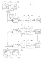
まず、本発明の好ましい実施例に係る発光ダイオード駆動回路2の模式図である図2Aを参照されたい。発光ダイオード駆動回路2は発光ダイオードモジュールLと併用される。このうち、発光ダイオード駆動回路2は読取りアドレス生成ユニット21と、メモリユニット22と、駆動ユニット23とを包括している。発光ダイオードモジュールLは少なくとも一つの発光ダイオードを包括しているが、ここで特に説明を要することは、発光ダイオードモジュールLの実際運用時には、使用するニーズまたは設計上の考慮に応じて、異なる数の発光ダイオードを有し、かつ発光ダイオード同士の接続方式もまたニーズに応じて変更してもよいということである。
Reference is first made to FIG. 2A, which is a schematic diagram of a light emitting
読取りアドレス生成ユニット21はシステム側(図示されない)からのクロック信号S1を受信するとともに、クロック信号S1に基づいてカウントを行い、特定のビットを指定して読み取るための信号である読取り信号S2を出力する。このうち、前記したシステム側は、例えば、他の回路または他の装置中に配設することができ、発光ダイオード駆動回路2とセットで運用されるパルス信号発生器である。
The read
本実施例において、クロック信号S1は二進重み付け(binary weighted)クロック信号であり、つまりは、図2Bに示すように、クロック信号S1の各パルスはその一つ前のパルスの時間幅を基準としており、二進方式で生成されるものであって、例えば一つ目のパルスの幅は20であり、二つ目のパルスの幅は21であり、三つ目のパルスの幅は22となっており、以下のパルスは順に倍増していく。このうち、パルスの幅は読取りアドレス生成ユニット21のカウンタの上限まで継続的に倍増していくものであり、例えば読取りアドレス生成ユニット21のカウント範囲が0ないし11であるとき、パルスの幅は211にまで倍増していった後に、パルスの幅が20にまで戻り、その後前記のような方式で順に倍増していくというものである。
In this embodiment, the clock signal S1 is a binary weighted clock signal, that is, as shown in FIG. 2B, each pulse of the clock signal S1 is based on the time width of the previous pulse. For example, the width of the first pulse is 2 0 , the width of the second pulse is 2 1 , and the width of the third pulse is 2 The following pulses are doubled in order. Of these, the pulse width is continuously doubled up to the upper limit of the counter of the read
メモリユニット22は読取りアドレス生成ユニット21に接続されるとともに、読取りアドレス生成ユニット21が出力した読取り信号S2に基づいて、特定のビットに対応する信号を選択し、グレイスケール信号を表す出力信号S3を出力する。実施上において、メモリユニット22はデュアルポートSRAM(Two Port SRAM)である。
The
駆動ユニット23はメモリユニット22に接続されるとともに、発光ダイオード駆動回路2が出力した出力信号S3およびシステム側(図示されない)が提供したクロック信号S1を受信して、発光ダイオードモジュールLに駆動信号S4を出力する。このうち、駆動ユニット23が受信したクロック信号S1および読取りアドレス生成ユニット21が受信したクロック信号S1は同一のパルス信号発生器を生成源としている。
The
実施上では、駆動信号S4はパルス幅変調信号であり、発光ダイオードモジュールLは駆動信号S4の導通期間に基づいて、異なるグレイスケールの輝度を発生させる。このうち、一動作周期において、駆動信号S4の導通期間は連続した導通期間とするか、または図2Bに示すように、駆動信号S4は動作期間T中に複数の導通期間T1を有し、且つ駆動信号S4が動作期間T中に複数の導通期間T1を有する場合、前記した導通期間T1は非連続状態としてもよい。したがって、駆動ユニット23は呈したいグレイスケール輝度に応じて、導通期間の幅を変調可能な駆動信号S4を出力するとともに、一動作周期において、駆動信号S4の導通期間を連続した導通期間とするか、または非連続の複数の導通期間としてもよい。
In practice, the drive signal S4 is a pulse width modulation signal, and the light emitting diode module L generates different gray scale luminances based on the conduction period of the drive signal S4. Among them, has in one operation cycle, or conduction period of the drive signal S4 is a continuous conduction period, or as shown in FIG. 2B, a plurality of the conduction period T 1 in the drive signal S4 operation period T, and when the drive signal S4 has a plurality of conduction period T 1 during operation T, conduction period T 1 described above may be a non-continuous state. Therefore, the
上記した構成により、発光ダイオード駆動回路2は大量のMOSFETから構成されるコンパレータを使用しなくても済むので、回路中における不要な電力損失を改善するとともに、回路の全体的な機能を高めている。特に説明しておくべきことは、メモリユニット22が12ビットのデュアルポートSRAMである場合、MOSFETは96個のみである。したがって、発光ダイオード駆動回路2は不要な電力損失を減らすのみならず、従来の発光ダイオード駆動回路1(図1Aに示す)と同じ駆動機能を実行するという条件下で、回路レイアウト(layout)で使用される面積を減らすことも可能である。
With the above-described configuration, the light emitting
続いて、図3を参照されたい。本発明の発光ダイオード駆動回路2をさらに詳しく説明する。本実施例において、読取りアドレス生成ユニット21は読取りアドレスカウンタ211と、読取りアドレスデコーダ212とを包括している。読取りアドレスカウンタ211はシステム側(図示されない)が提供したクロック信号S1を受信するとともに、クロック信号S1に基づいてカウントを行うとともにその結果を出力する。読取りアドレスデコーダ212は読取りアドレスカウンタ211に接続されるとともに、読取りアドレスカウンタ211が出力した結果に基づいて読取り信号S2を生成する。
Next, please refer to FIG. The light emitting
駆動ユニット23はフリップフロップ231と、ドライバ232とを包括している。フリップフロップ231はメモリユニット22に接続されるとともに、メモリユニット22が生成した出力信号S3およびシステム側(図示されない)が提供したクロック信号S1を受信する。ドライバ232はフリップフロップ231に接続されるとともに、発光ダイオードモジュールLに駆動信号S4を出力する。実施上において、フリップフロップ231はD型フリップフロップであり、ドライバ232は例えばMOSFETであり、且つドライバ232は定電流源によって発光ダイオードモジュールLに駆動信号S4を出力することができる。
The
また、発光ダイオード駆動回路2は書込みアドレス生成ユニット24と、シフトレジスタ25とをさらに包括している。書込みアドレス生成ユニット24はメモリユニット22に接続されるとともに、書込みアドレスカウンタ241と書込みアドレスデコーダ242とを包括している。このうち、書込みアドレスカウンタ241はシステム側(図示されない)が提供したラッチイネーブル信号S5を受信するとともに、カウントを行う。書込みアドレスデコーダ242は書込みアドレスカウンタ241に接続されるとともに、書込みアドレスカウンタ241の出力に基づいて書込み信号S6を生成する。書込みアドレスデコーダ242は書込み信号S6をメモリユニット22に送信する。シフトレジスタ25はメモリユニット22に接続されるとともに、クロック信号S7および入力信号S8を受信して、メモリユニット22にグレイスケール信号S9を提供する。メモリユニット22は書込み信号S6に基づいてグレイスケール信号S9を特定のアドレスに書き込む。このうち、シフトレジスタ25が受信したクロック信号S7は、駆動ユニット23および読取りアドレス生成ユニット21が受信したクロック信号S1とは異なるパルス信号発生器を生成源としているので、クロック信号S7およびクロック信号S1は完全に異なる波形を有している。また、入力信号S8はグレイスケール情報を表す信号であって、グレイスケール信号S9とは実質的に同じである。
The light emitting
注目すべきは、本実施例において、メモリユニット22はデュアルポートSRAMであり、且つメモリユニット22はシフトレジスタ25の入力ポートに接続されて書込み機能のみが許可されているということである。また、データの書込み時には、パラレル伝送の方式でデータをメモリユニット22に書込み、データの読取り時には、特定の単一ビットを読み取る。したがって、メモリユニット22はデータを書き込む間に、同一アドレスのデータを読み取ることも可能であるため、データの書込み完了を待たずとも、読取り動作を行うことができる。換言すると、メモリユニット22は、二つの異なるクロック信号系による同一アドレスへの書込みおよび読取りを同時に許可するとともに、待つ必要はなくなるため、回路の複雑度を低減することができるということになる。
It should be noted that in this embodiment, the
続いて、図4のフローチャートを参照するとともに、図2A、図2Bおよび図3を合せて、本発明の好ましい実施例の発光ダイオードモジュールの駆動方法を説明する。この方法は上記した発光ダイオード駆動回路2および発光ダイオードモジュールLと併用されるものであって、駆動方法の工程は工程S01〜工程S03を含んでいる。
Subsequently, while referring to the flowchart of FIG. 4, a driving method of the light emitting diode module according to the preferred embodiment of the present invention will be described with reference to FIGS. 2A, 2B and 3. FIG. This method is used in combination with the light emitting
工程S01では、読取りアドレス生成ユニット21によりクロック信号を受信するとともに、メモリユニット22に読取り信号S2を出力する。本実施例において、読取りアドレス生成ユニット21はシステム側からの、例えばパルス信号発生器が生成したクロック信号S1を受信してカウントを行うので、メモリユニット22に読取り信号S2を出力する。前記したクロック信号S1は二進重み付けクロック信号、つまり、クロック信号S1の各パルスはその一つ前のパルスの時間幅を基準として、二進方式で生成されるものであって、且つパルスの幅は読取りアドレス生成ユニット21のカウンタの上限まで継続的に倍増していき、さらに初期値に戻る。
In step S01, the read
工程S02では、メモリユニット22により読取り信号S2に基づいて出力信号S3を生成する。本実施例において、メモリユニット22は、読取り信号S2に基づいて、特定のビットに対応する信号を選択し、グレイスケール信号を表す出力信号S3を出力する。このうち、メモリユニット22はデュアルポートSRAMである。
In step S02, the
工程S03では、駆動ユニット23により出力信号S3およびクロック信号S1を受信するとともに、発光ダイオードモジュールLに駆動信号S4を出力する。本実施例において、駆動ユニット23はメモリユニット22が出力した出力信号S3およびシステム側が提供したクロック信号S1を受信するので、発光ダイオードモジュールLに駆動信号S4を出力する。このうち、駆動信号S4はパルス幅変調信号であり、かつ実施上において、一動作周期において、駆動信号S4の導通期間は連続した導通期間、または非連続の複数の導通期間としてもよい。
In step S03, the
一動作周期において、もし非連続の導通期間の合計が連続した導通期間の合計と同じである場合、人の目で感じられる輝度は同じである。したがって、上記した駆動方法により、本発明では非連続の導通期間または連続した導通期間として駆動信号S4を変調することで、発光ダイオードモジュールLのグレイスケールでの制御を実現している。 In one operation cycle, if the sum of discontinuous conduction periods is the same as the sum of consecutive conduction periods, the luminance perceived by the human eye is the same. Therefore, in the present invention, the drive signal S4 is modulated as a discontinuous conduction period or a continuous conduction period by the above-described driving method, thereby realizing the gray scale control of the light emitting diode module L.
また、駆動方法は、書込みアドレス生成ユニット24によりラッチイネーブル信号S5に基づいてメモリユニット22に書込み信号S6を出力する、ことをさらに含む。本実施例において、書込みアドレス生成ユニット24はシステム側が提供したラッチイネーブル信号S5を受信してカウントを行うので、メモリユニット22に書込み信号S6を出力することで、メモリユニット22にてシフトレジスタ25からのグレイスケール信号S9を書き込む。このうち、前記したシステム側は例えば発光ダイオード駆動回路2と併用される信号発生器である。
The driving method further includes outputting the write signal S6 to the
続いて、本発明の好ましい実施例に係る発光ダイオード駆動装置3である図5を参照されたい。発光ダイオード駆動装置3は複数の発光ダイオードモジュールLと組み合わされる。発光ダイオード駆動装置3は複数のメモリユニット31と、書込みアドレス生成ユニット32と、読取りアドレス生成ユニット33と、複数の駆動ユニット34とを包括している。
Next, please refer to FIG. 5 which is a light emitting
メモリユニット31は並列接続方式で接続されており、本実施例においては、各メモリユニット31がそれぞれ12ビットのデュアルポートSRAMであるとともに、発光ダイオード駆動装置3はメモリユニット31を合計16個包括しているものを例としているが、これに限定されるものではない。
The
書込みアドレス生成ユニット32はシステム側が提供したラッチイネーブル信号S5に基づいて書込み信号S6を生成する。このうち、書込みアドレス生成ユニット32は書込みアドレスカウンタ321と、書込みアドレスデコーダ322とを包括している。書込みアドレスカウンタ321は4ビットの書込みアドレスカウンタであって、書込みアドレスデコーダ322は4イン16アウトの書込みアドレスデコーダである。書込みアドレスカウンタ321はラッチイネーブル信号S5に基づいてカウントを行い、書込みアドレスデコーダ322を介して書込み信号S6を生成することで、グレイスケール信号S9を16個のメモリユニット31のうちの一つに書き込む。換言すると、書込み信号S6はグレイスケール信号S9を書き込むメモリユニット31を指定するためのものである。
The write
読取りアドレス生成ユニット33はシステム側が提供したクロック信号S1を受信するとともに各メモリユニット31に読取り信号S2を出力する。本実施例において、読取りアドレス生成ユニット33は読取りアドレスカウンタ331と、読取りアドレスデコーダ332とを包括している。読取りアドレスカウンタ331は4ビットの読取りアドレスカウンタであって、読取りアドレスデコーダ332は4イン12アウトの読取りアドレスデコーダである。システム側が提供したクロック信号S1は読取りアドレスカウンタ331の駆動に用いられ、読取りアドレスデコーダ332は読取りアドレスカウンタ331の出力を受け取ることで、ある指定されたビットを選択して、全てのメモリユニット31に読取り信号S2を出力する。
The read
前記したクロック信号S1は二進重み付けクロック信号であり、クロック信号S1の各パルスはその一つ前のパルスの時間幅を基準として、二進方式で生成されるものであって、且つパルスの幅は読取りアドレスカウンタ331のカウンタの上限まで継続的に倍増していき、さらに初期値に戻る。
The aforementioned clock signal S1 is a binary weighted clock signal, and each pulse of the clock signal S1 is generated in a binary system based on the time width of the previous pulse, and the pulse width Continuously doubles to the upper limit of the counter of the read
各駆動ユニット34はフリップフロップ341と、ドライバ342とをそれぞれ包括している。各フリップフロップ341は対応するメモリユニット31にそれぞれ接続されるとともに、出力信号S3およびクロック信号S1を受信する。このうち、駆動ユニット34が受信したクロック信号S1は同一のパルス信号発生器を生成源としている。ドライバ342はフリップフロップ341に接続されるとともに、定電流の方式で発光ダイオードモジュールLに駆動信号S4を出力する。このうち、駆動信号S4はパルス幅変調信号であり、かつ実施上において、一動作周期において、駆動信号S4の導通期間は連続した導通期間、または非連続の複数の導通期間としてもよい。
Each
また、発光ダイオード駆動装置3は、各メモリユニット31に接続されるとともに、クロック信号S7および入力信号S8を受信して、各メモリユニット31にグレイスケール信号S9を提供するシフトレジスタ35も包括している。このうち、シフトレジスタ35が受信したクロック信号S7は、駆動ユニット34および読取りアドレス生成ユニット33が受信したクロック信号S1とは異なるパルス信号発生器を生成源としている。また、入力信号S8はグレイスケール情報を表す信号であって、グレイスケール信号S9とは実質的に同じである。
In addition, the light emitting
本実施例において、各メモリユニット31はシフトレジスタ35の入力ポートに接続されて書込み機能のみ許可されている。また、データの書込み時には、パラレル伝送の方式でデータをこのうちの一つのメモリユニット31に書込み、データの読取り時には、特定の単一ビットを読み取る。したがって、メモリユニット31はデータを書き込む間に、同一アドレスのデータを読み取ることも可能であるため、データの書込み完了を待たずとも、読取り動作を行うことができる。換言すると、メモリユニット31は、二つの異なるクロック信号系による同一アドレスへの書込みおよび読取りを同時に許可するとともに、待つ必要はなくなるため、回路の複雑度を低減することができる。
In this embodiment, each
注目すべきは、上記したような規格のメモリユニット31、書込みアドレスカウンタ321、書込みアドレスデコーダ322、読取りアドレスカウンタ331および読取りアドレスデコーダ332を採用する場合、4096階調のグレイスケールを発生させるという条件にて、前記した素子は合計約2000個のMOSFETを含むことになるということである。しかしながら、もし従来の発光ダイオード駆動回路1を使用するならば、4096階調のグレイスケールを発生させるという条件にて、少なくとも17000個のMOSFETが必要となる。したがって、本発明の発光ダイオード駆動装置3はMOSFETの使用を減らしているので、不要な電力損失を減らし、且つダイサイズ(die size)の縮小が顕著となり、且つ装置を効果的に小型化できる。
It should be noted that, when the
続いて、図6のフローチャートを参照するとともに図5を合せて、本発明の好ましい実施例の発光ダイオードモジュールの駆動方法を説明する。この方法は上記した発光ダイオード駆動装置3および複数の発光ダイオードモジュールLと併用されるものであって、駆動方法の工程は工程S11〜工程S13を含んでいる。
Next, referring to the flowchart of FIG. 6 and FIG. 5, a method of driving the light emitting diode module according to the preferred embodiment of the present invention will be described. This method is used in combination with the above-described light emitting
工程S11では、読取りアドレス生成ユニット33によりクロック信号S1を受信するとともに、各メモリユニット31に読取り信号S2を出力する。本実施例において、システム側が提供したクロック信号S1は読取りアドレス生成ユニット33を駆動して、全てのメモリユニット31に読取り信号S2を出力する。このうち、クロック信号S1は二進重み付けクロック信号である。
In step S11, the read
工程S12では、各メモリユニット31により読取り信号S2に基づいて対応する駆動ユニット34に出力信号S3を出力する。本実施例において、全てのメモリユニット31は、読取り信号S2に基づいて、特定のビットに対応する信号を選択して、出力信号S3を生成する。このうち、メモリユニット31はデュアルポートSRAMである。
In step S12, each
工程S13では、各駆動ユニット34により出力信号S3およびクロック信号S1を受信するとともに、発光ダイオードモジュールLに駆動信号S4を出力する。本実施例において、駆動ユニット34は出力信号S3およびクロック信号S1を受信するので、対応する発光ダイオードモジュールLに駆動信号S4を出力するとともに、発光ダイオードモジュールLは駆動信号S4の導通期間に基づいて対応するグレイスケール輝度を発生させる。また、駆動方法は、書込みアドレス生成ユニット32がラッチイネーブル信号S5に基づいて書込み信号S6を生成することと、メモリユニット31のうちの一つが書込み信号S6に基づいてグレイスケール信号S9を書き込むことと、をさらに含む。
In step S13, each
上記をまとめるに、本発明の発光ダイオード駆動回路、発光ダイオード駆動装置および駆動方法によれば、メモリユニットは読取りアドレス生成ユニットが出力した読取り信号に基づいて出力信号を生成するとともに、駆動ユニットが出力信号およびクロック信号に基づいて発光ダイオードモジュールを駆動するので、不要な電力損失を減らすとともに、処理効率を高めることができる。 In summary, according to the light emitting diode driving circuit, the light emitting diode driving device and the driving method of the present invention, the memory unit generates an output signal based on the read signal output from the read address generating unit, and the drive unit outputs the output signal. Since the light emitting diode module is driven based on the signal and the clock signal, unnecessary power loss can be reduced and the processing efficiency can be increased.
上記は例示的なものであって、限定するためのものではない。本発明の技術的思想および範囲から逸脱することなく、行われる等価の修正または変更は、いずれも後記の特許請求の範囲に含まれる。 The above is illustrative and not limiting. Any equivalent modifications or changes made without departing from the spirit and scope of the present invention will fall within the scope of the following claims.
本発明は以上のように構成しているため、不要な電力損失を減らすとともに、処理効率を高めることができる発光ダイオード駆動回路、発光ダイオード駆動装置および駆動方法を提供し得るものである。 Since the present invention is configured as described above, it is possible to provide a light emitting diode driving circuit, a light emitting diode driving device, and a driving method that can reduce unnecessary power loss and increase processing efficiency.
2 発光ダイオード駆動回路
232、342 ドライバ
21、33 読取りアドレス生成ユニット
211、331 読取りアドレスカウンタ
212、332 読取りアドレスデコーダ
22、31 メモリユニット
23、34 駆動ユニット
231、341 フリップフロップ
24、32 書込みアドレス生成ユニット
241、321 書込みアドレスカウンタ
242、322 書込みアドレスデコーダ
25、35 シフトレジスタ
3 発光ダイオード駆動装置
L 発光ダイオードモジュール
S01〜S03、S11〜S13 駆動方法の工程
S1、S7 クロック信号
S2 読取り信号
S3 出力信号
S4 駆動信号
S5 ラッチイネーブル信号
S6 書込み信号
S8 入力信号
S9 グレイスケール信号
T 動作周期
T1 導通期間
2
Claims (15)
クロック信号を受信するとともに読取り信号を出力する読取りアドレス生成ユニットと、
前記読取りアドレス生成ユニットに接続されるとともに、前記読取り信号に基づいて出力信号を生成するメモリユニットと、
前記メモリユニットに接続されるとともに、前記出力信号および前記クロック信号を受信して、前記発光ダイオードモジュールに駆動信号を出力する駆動ユニットと、を包括し、
前記駆動ユニットは、前記メモリユニットに接続されるとともに、前記出力信号および前記クロック信号を受信するフリップフロップと、前記フリップフロップに接続されるとともに、前記出力信号および前記クロック信号に基いて前記駆動信号を出力するドライバとから成り、
前記クロック信号が二進重み付けクロック信号であることを特徴とする発光ダイオード駆動回路。 A light emitting diode driving circuit combined with a light emitting diode module,
A read address generation unit that receives a clock signal and outputs a read signal;
A memory unit connected to the read address generation unit and generating an output signal based on the read signal;
A drive unit connected to the memory unit and receiving the output signal and the clock signal and outputting a drive signal to the light emitting diode module ;
The drive unit is connected to the memory unit and receives the output signal and the clock signal. The drive unit is connected to the flip-flop, and the drive signal is based on the output signal and the clock signal. And a driver that outputs
A light emitting diode driving circuit, wherein the clock signal is a binary weighted clock signal .
前記クロック信号を受信する読取りアドレスカウンタと、
前記読取りアドレスカウンタに接続されるとともに、前記読取り信号を出力する読取りアドレスデコーダと、を包括していることを特徴とする請求項1に記載の発光ダイオード駆動回路。 The read address generation unit is
A read address counter for receiving the clock signal;
2. The light emitting diode driving circuit according to claim 1, further comprising a read address decoder connected to the read address counter and outputting the read signal.
前記メモリユニットに接続されているシフトレジスタと、をさらに包括していることを特徴とする請求項1に記載の発光ダイオード駆動回路。 A write address generation unit connected to the memory unit and outputting a write signal to the memory unit based on a latch enable signal;
The light emitting diode driving circuit according to claim 1, further comprising a shift register connected to the memory unit.
前記ラッチイネーブル信号を受信する書込みアドレスカウンタと、
前記書込みアドレスカウンタに接続されるとともに、前記書込み信号を出力する書込みアドレスデコーダとを包括していることを特徴とする請求項5に記載の発光ダイオード駆動回路。 The write address generation unit
A write address counter that receives the latch enable signal;
6. The light emitting diode driving circuit according to claim 5 , further comprising a write address decoder connected to the write address counter and outputting the write signal.
前記読取りアドレス生成ユニットがクロック信号を受信するとともに、前記メモリユニットに読取り信号を出力する工程と、
前記メモリユニットが前記読取り信号に基づいて、出力信号を生成する工程と、
前記駆動ユニットが前記出力信号および前記クロック信号を受信するとともに、発光ダイオードモジュールに前記駆動信号を出力する工程と、を包括し、
前記駆動ユニットは、前記メモリユニットに接続されるとともに、前記出力信号および前記クロック信号を受信するフリップフロップと、前記フリップフロップに接続されるとともに、前記出力信号および前記クロック信号に基いて前記駆動信号を出力するドライバとから成り、
前記クロック信号が二進重み付けクロック信号であることを特徴とする発光ダイオードモジュールの駆動方法。 A light emitting diode module driving method combined with a light emitting diode driving circuit having a read address generation unit, a memory unit, and a driving unit,
The read address generation unit receiving a clock signal and outputting a read signal to the memory unit;
The memory unit generating an output signal based on the read signal;
The drive unit receiving the output signal and the clock signal and outputting the drive signal to a light emitting diode module ,
The drive unit is connected to the memory unit and receives the output signal and the clock signal. The drive unit is connected to the flip-flop, and the drive signal is based on the output signal and the clock signal. And a driver that outputs
The method of driving a light emitting diode module, wherein the clock signal is a binary weighted clock signal .
並列接続されている複数のメモリユニットと、
ラッチイネーブル信号に基づいて書込み信号を生成する書込みアドレス生成ユニットと、
クロック信号を受信するとともに前記メモリユニットのそれぞれに読取り信号を出力する読取りアドレス生成ユニットと、
対応するメモリユニットにそれぞれ接続されている複数の駆動ユニットと、を含んでおり、
各駆動ユニットは、各メモリユニットにそれぞれ接続されるとともに、前記出力信号および前記クロック信号を受信するフリップフロップと、当該フリップフロップに接続されるとともに、前記出力信号および前記クロック信号に基いて前記駆動信号を出力するドライバとから成り、
これらメモリユニットのうちの一つは前記書込み信号に基づいてグレイスケール信号を書き込み、前記メモリユニットのそれぞれは前記読取り信号に基づいて対応する発光ダイオードモジュールに駆動信号を出力し、前記駆動ユニットの各々は前記出力信号および前記クロック信号に基づいて、対応する発前記光ダイオードモジュールに駆動信号を出力し、前記クロック信号が二進重み付けクロック信号であることを特徴とする発光ダイオード駆動装置。 A light emitting diode driving device combined with a plurality of light emitting diode modules,
A plurality of memory units connected in parallel;
A write address generation unit for generating a write signal based on the latch enable signal;
A read address generation unit that receives a clock signal and outputs a read signal to each of the memory units;
A plurality of drive units each connected to a corresponding memory unit,
Each drive unit is connected to each memory unit, receives the output signal and the clock signal, and is connected to the flip-flop, and is driven based on the output signal and the clock signal. Consisting of a driver that outputs signals,
One of these memory units writes a grayscale signal based on the write signal, each of the memory units outputs a drive signal to a corresponding light emitting diode module based on the read signal, and each of the drive units Outputs a drive signal to the corresponding light emitting diode module based on the output signal and the clock signal, and the clock signal is a binary weighted clock signal .
前記クロック信号を受信する読取りアドレスカウンタと、
前記読取りアドレスカウンタに接続されるとともに、前記読取り信号を出力する読取りアドレスデコーダと、を包括することを特徴とする請求項9に記載の発光ダイオード駆動装置。 The read address generation unit is
A read address counter for receiving the clock signal;
The light emitting diode driving device according to claim 9 , further comprising: a read address decoder connected to the read address counter and outputting the read signal.
前記ラッチイネーブル信号を受信する書込みアドレスカウンタと、
前記書込みアドレスカウンタに接続されるとともに、前記書込み信号を出力する書込みアドレスデコーダと、を包括することを特徴とする請求項9に記載の発光ダイオード駆動装置。 The write address generation unit is
A write address counter that receives the latch enable signal;
The light emitting diode driving device according to claim 9 , further comprising a write address decoder connected to the write address counter and outputting the write signal.
前記読取りアドレス生成ユニットがクロック信号を受信するとともに、前記メモリユニットのそれぞれに読取り信号を出力する工程と、
前記メモリユニットのそれぞれが前記読取り信号に基づいて、対応する前記駆動ユニットに出力信号を出力する工程と、
前記駆動ユニットのそれぞれが前記出力信号および前記クロック信号に基づいて、対応する前記発光ダイオードモジュールに前記駆動信号を出力する工程と、を包括し、
各駆動ユニットは、各メモリユニットにそれぞれ接続されるとともに、前記出力信号および前記クロック信号を受信するフリップフロップと、当該フリップフロップに接続されるとともに、前記出力信号および前記クロック信号に基いて前記駆動信号を出力するドライバとから成り、
前記クロック信号が二進重み付けクロック信号であることを特徴とする発光ダイオードモジュールの駆動方法。 A method of driving a light emitting diode module combined with a light emitting diode driving device including a plurality of memory units, a write address generating unit, a read address generating unit, and a plurality of driving units,
The read address generation unit receives a clock signal and outputs a read signal to each of the memory units;
Each of the memory units outputting an output signal to the corresponding drive unit based on the read signal;
Each of the drive units outputting the drive signal to the corresponding light emitting diode module based on the output signal and the clock signal ,
Each drive unit is connected to each memory unit, receives the output signal and the clock signal, and is connected to the flip-flop, and is driven based on the output signal and the clock signal. Consisting of a driver that outputs signals,
The method of driving a light emitting diode module, wherein the clock signal is a binary weighted clock signal .
これらメモリユニットのうちの一つは前記書込み信号に基づいてグレイスケール信号を書き込む工程と、をさらに包括することを特徴とする請求項14に記載の駆動方法。 The write address generation unit generating a write signal based on a latch enable signal;
15. The driving method according to claim 14 , wherein one of the memory units further includes a step of writing a gray scale signal based on the write signal.
Applications Claiming Priority (2)
| Application Number | Priority Date | Filing Date | Title |
|---|---|---|---|
| TW101115237 | 2012-04-27 | ||
| TW101115237A TWI581658B (en) | 2012-04-27 | 2012-04-27 | Led driving circuit, led driving device and driving method |
Publications (2)
| Publication Number | Publication Date |
|---|---|
| JP2013232615A JP2013232615A (en) | 2013-11-14 |
| JP5643268B2 true JP5643268B2 (en) | 2014-12-17 |
Family
ID=49476673
Family Applications (1)
| Application Number | Title | Priority Date | Filing Date |
|---|---|---|---|
| JP2012196985A Expired - Fee Related JP5643268B2 (en) | 2012-04-27 | 2012-09-07 | Light emitting diode driving circuit, light emitting diode driving device and driving method |
Country Status (3)
| Country | Link |
|---|---|
| US (1) | US9271360B2 (en) |
| JP (1) | JP5643268B2 (en) |
| TW (1) | TWI581658B (en) |
Families Citing this family (5)
| Publication number | Priority date | Publication date | Assignee | Title |
|---|---|---|---|---|
| CN108364603B (en) * | 2018-01-19 | 2020-03-31 | 宗仁科技(平潭)有限公司 | LED lamp-based addressing method, addressing device and terminal equipment |
| TWI698684B (en) * | 2018-08-01 | 2020-07-11 | 台灣光罩股份有限公司 | Led module, display and calibration system with traceability |
| US11056029B1 (en) | 2020-01-08 | 2021-07-06 | Weida Hi-Tech Corporation Ltd. | LED module, display and calibration system with traceability |
| CN111210781B (en) * | 2020-03-09 | 2022-10-14 | 诺肯科技股份有限公司 | LED backlight driving circuit and address setting method thereof |
| WO2021195838A1 (en) * | 2020-03-30 | 2021-10-07 | 京东方科技集团股份有限公司 | Pixel structure and driving method therefor, and display apparatus |
Family Cites Families (17)
| Publication number | Priority date | Publication date | Assignee | Title |
|---|---|---|---|---|
| JPS6231893A (en) * | 1985-08-02 | 1987-02-10 | 沖電気工業株式会社 | Driving circuit for light emitting element and light quantity controlling element |
| JPH01196345A (en) * | 1988-01-30 | 1989-08-08 | Canon Inc | Image forming device |
| US5668568A (en) * | 1992-11-13 | 1997-09-16 | Trans-Lux Corporation | Interface for LED matrix display with buffers with random access input and direct memory access output |
| JP2838015B2 (en) * | 1993-04-20 | 1998-12-16 | ローム株式会社 | Print head |
| JPH09330046A (en) * | 1996-04-04 | 1997-12-22 | Sony Corp | Display device and its method |
| JPH09319332A (en) * | 1996-05-27 | 1997-12-12 | Matsushita Electric Ind Co Ltd | Led display device and led display method |
| JP3702699B2 (en) * | 1999-03-26 | 2005-10-05 | 三菱電機株式会社 | Color image display device |
| US7292209B2 (en) * | 2000-08-07 | 2007-11-06 | Rastar Corporation | System and method of driving an array of optical elements |
| JP2002268606A (en) * | 2001-03-07 | 2002-09-20 | Pioneer Electronic Corp | Method for driving luminescent display and its device |
| JP3596516B2 (en) * | 2001-11-20 | 2004-12-02 | 日本電気株式会社 | Electronic device with display |
| JP4134755B2 (en) * | 2003-02-28 | 2008-08-20 | ヤマハ株式会社 | Speaker array drive device |
| US7246199B2 (en) * | 2003-05-29 | 2007-07-17 | Elantec Semiconductor, Inc. | Double buffering of serial transfers |
| TWI277024B (en) | 2005-05-10 | 2007-03-21 | Synage Technology Corp | Programmable light emitting diode device |
| TWI400003B (en) * | 2008-11-24 | 2013-06-21 | Holtek Semiconductor Inc | Light emitting diode control drive |
| JP2010140953A (en) * | 2008-12-09 | 2010-06-24 | Sanyo Electric Co Ltd | Light-emitting element driving circuit |
| US20120299480A1 (en) * | 2009-11-06 | 2012-11-29 | Neofocal Systems, Inc. | System And Method For Current Modulated Data Transmission |
| JP5556287B2 (en) * | 2010-03-24 | 2014-07-23 | 株式会社Jvcケンウッド | Projection display |
-
2012
- 2012-04-27 TW TW101115237A patent/TWI581658B/en not_active IP Right Cessation
- 2012-09-07 JP JP2012196985A patent/JP5643268B2/en not_active Expired - Fee Related
- 2012-09-14 US US13/617,972 patent/US9271360B2/en not_active Expired - Fee Related
Also Published As
| Publication number | Publication date |
|---|---|
| JP2013232615A (en) | 2013-11-14 |
| TW201345311A (en) | 2013-11-01 |
| US20130285570A1 (en) | 2013-10-31 |
| TWI581658B (en) | 2017-05-01 |
| US9271360B2 (en) | 2016-02-23 |
Similar Documents
| Publication | Publication Date | Title |
|---|---|---|
| US8760458B2 (en) | Scan-type display device control circuit | |
| KR102587794B1 (en) | Image Display Apparatus and Driving Method Thereof | |
| JP5643268B2 (en) | Light emitting diode driving circuit, light emitting diode driving device and driving method | |
| KR102328594B1 (en) | Display appartus including micro LED | |
| TWI410930B (en) | Led driver and led driving system | |
| KR102535805B1 (en) | Driver for display panel and display apparatus having the same | |
| KR102108516B1 (en) | Device with mip(memory inside pixel) display | |
| CN111583857B (en) | Pixel driving circuit, driving method thereof and display panel | |
| JP5935192B2 (en) | Method for controlling light emission of a light emitting device | |
| CN112017589A (en) | Multi-gray-scale pixel driving circuit and display panel | |
| US9953580B2 (en) | OLED gate driving circuit structure | |
| CN102157130A (en) | Pulse width modulating method for LED driving integrated circuit | |
| TWI491304B (en) | Led driver circuit and driver system | |
| CN112967665B (en) | Light emitting element control circuit, display panel and display device | |
| WO2023126027A2 (en) | Driver circuit of display panel | |
| TWI507079B (en) | Driving apparatus of light emitting diode and driving method thereof | |
| WO2012022235A1 (en) | Method and device for frequency multiplication of display control | |
| CN101964171B (en) | Data transmission method | |
| KR100637393B1 (en) | Circuit and method for adjusting brightness of display device | |
| US10460650B2 (en) | Display device, driving method thereof, and non-transitory computer readable recording medium | |
| TWI627617B (en) | Display device | |
| CN103379702B (en) | LED driving circuit, light emitting diode drive device and driving method | |
| US9549439B2 (en) | Display apparatus and method of driving backlight thereof | |
| KR102302793B1 (en) | Device with mip(memory inside pixel) display | |
| WO2023206277A1 (en) | Circuit assembly, electronic device and driving method |
Legal Events
| Date | Code | Title | Description |
|---|---|---|---|
| A977 | Report on retrieval |
Free format text: JAPANESE INTERMEDIATE CODE: A971007 Effective date: 20140129 |
|
| A131 | Notification of reasons for refusal |
Free format text: JAPANESE INTERMEDIATE CODE: A131 Effective date: 20140225 |
|
| A601 | Written request for extension of time |
Free format text: JAPANESE INTERMEDIATE CODE: A601 Effective date: 20140521 |
|
| A602 | Written permission of extension of time |
Free format text: JAPANESE INTERMEDIATE CODE: A602 Effective date: 20140526 |
|
| A521 | Written amendment |
Free format text: JAPANESE INTERMEDIATE CODE: A523 Effective date: 20140619 |
|
| TRDD | Decision of grant or rejection written | ||
| A01 | Written decision to grant a patent or to grant a registration (utility model) |
Free format text: JAPANESE INTERMEDIATE CODE: A01 Effective date: 20141021 |
|
| A61 | First payment of annual fees (during grant procedure) |
Free format text: JAPANESE INTERMEDIATE CODE: A61 Effective date: 20141030 |
|
| R150 | Certificate of patent or registration of utility model |
Ref document number: 5643268 Country of ref document: JP Free format text: JAPANESE INTERMEDIATE CODE: R150 |
|
| R250 | Receipt of annual fees |
Free format text: JAPANESE INTERMEDIATE CODE: R250 |
|
| LAPS | Cancellation because of no payment of annual fees |