JP5587558B2 - Photoelectric conversion device - Google Patents
Photoelectric conversion device Download PDFInfo
- Publication number
- JP5587558B2 JP5587558B2 JP2009064283A JP2009064283A JP5587558B2 JP 5587558 B2 JP5587558 B2 JP 5587558B2 JP 2009064283 A JP2009064283 A JP 2009064283A JP 2009064283 A JP2009064283 A JP 2009064283A JP 5587558 B2 JP5587558 B2 JP 5587558B2
- Authority
- JP
- Japan
- Prior art keywords
- film
- diode
- terminal
- photodiode
- current
- Prior art date
- Legal status (The legal status is an assumption and is not a legal conclusion. Google has not performed a legal analysis and makes no representation as to the accuracy of the status listed.)
- Expired - Fee Related
Links
- 238000006243 chemical reaction Methods 0.000 title claims description 10
- 239000004065 semiconductor Substances 0.000 claims description 248
- 239000010408 film Substances 0.000 description 668
- 239000000758 substrate Substances 0.000 description 123
- 238000000034 method Methods 0.000 description 72
- 230000001681 protective effect Effects 0.000 description 52
- 239000010410 layer Substances 0.000 description 48
- XUIMIQQOPSSXEZ-UHFFFAOYSA-N Silicon Chemical compound [Si] XUIMIQQOPSSXEZ-UHFFFAOYSA-N 0.000 description 46
- 229910052710 silicon Inorganic materials 0.000 description 46
- 239000010703 silicon Substances 0.000 description 46
- 239000007789 gas Substances 0.000 description 44
- 239000012535 impurity Substances 0.000 description 37
- 238000005530 etching Methods 0.000 description 36
- 229910052581 Si3N4 Inorganic materials 0.000 description 32
- HQVNEWCFYHHQES-UHFFFAOYSA-N silicon nitride Chemical compound N12[Si]34N5[Si]62N3[Si]51N64 HQVNEWCFYHHQES-UHFFFAOYSA-N 0.000 description 32
- PXHVJJICTQNCMI-UHFFFAOYSA-N Nickel Chemical compound [Ni] PXHVJJICTQNCMI-UHFFFAOYSA-N 0.000 description 29
- 239000001257 hydrogen Substances 0.000 description 29
- 229910052739 hydrogen Inorganic materials 0.000 description 29
- 238000004519 manufacturing process Methods 0.000 description 27
- 239000013078 crystal Substances 0.000 description 26
- 238000010438 heat treatment Methods 0.000 description 25
- VYPSYNLAJGMNEJ-UHFFFAOYSA-N silicon dioxide Inorganic materials O=[Si]=O VYPSYNLAJGMNEJ-UHFFFAOYSA-N 0.000 description 25
- 230000015556 catabolic process Effects 0.000 description 24
- 230000002829 reductive effect Effects 0.000 description 24
- 239000010936 titanium Substances 0.000 description 24
- UFHFLCQGNIYNRP-UHFFFAOYSA-N Hydrogen Chemical compound [H][H] UFHFLCQGNIYNRP-UHFFFAOYSA-N 0.000 description 23
- IJGRMHOSHXDMSA-UHFFFAOYSA-N Atomic nitrogen Chemical compound N#N IJGRMHOSHXDMSA-UHFFFAOYSA-N 0.000 description 22
- 229910052760 oxygen Inorganic materials 0.000 description 22
- 239000001301 oxygen Substances 0.000 description 22
- 229910052814 silicon oxide Inorganic materials 0.000 description 22
- QVGXLLKOCUKJST-UHFFFAOYSA-N atomic oxygen Chemical compound [O] QVGXLLKOCUKJST-UHFFFAOYSA-N 0.000 description 21
- 239000002585 base Substances 0.000 description 20
- XKRFYHLGVUSROY-UHFFFAOYSA-N Argon Chemical compound [Ar] XKRFYHLGVUSROY-UHFFFAOYSA-N 0.000 description 18
- 239000000463 material Substances 0.000 description 18
- 229910052719 titanium Inorganic materials 0.000 description 18
- 229910052721 tungsten Inorganic materials 0.000 description 18
- 239000010937 tungsten Substances 0.000 description 18
- RTAQQCXQSZGOHL-UHFFFAOYSA-N Titanium Chemical compound [Ti] RTAQQCXQSZGOHL-UHFFFAOYSA-N 0.000 description 17
- 230000004888 barrier function Effects 0.000 description 17
- 238000002425 crystallisation Methods 0.000 description 17
- 238000010586 diagram Methods 0.000 description 17
- 238000005268 plasma chemical vapour deposition Methods 0.000 description 17
- WFKWXMTUELFFGS-UHFFFAOYSA-N tungsten Chemical compound [W] WFKWXMTUELFFGS-UHFFFAOYSA-N 0.000 description 17
- 238000005229 chemical vapour deposition Methods 0.000 description 16
- 230000006870 function Effects 0.000 description 16
- 238000004544 sputter deposition Methods 0.000 description 16
- 230000008025 crystallization Effects 0.000 description 15
- 230000006866 deterioration Effects 0.000 description 15
- BASFCYQUMIYNBI-UHFFFAOYSA-N platinum Chemical compound [Pt] BASFCYQUMIYNBI-UHFFFAOYSA-N 0.000 description 15
- BLRPTPMANUNPDV-UHFFFAOYSA-N Silane Chemical compound [SiH4] BLRPTPMANUNPDV-UHFFFAOYSA-N 0.000 description 14
- 239000010931 gold Substances 0.000 description 14
- 230000002265 prevention Effects 0.000 description 14
- 239000011521 glass Substances 0.000 description 13
- 229910052750 molybdenum Inorganic materials 0.000 description 13
- 239000011733 molybdenum Substances 0.000 description 13
- 239000011347 resin Substances 0.000 description 13
- 229920005989 resin Polymers 0.000 description 13
- 229910000077 silane Inorganic materials 0.000 description 13
- ZOKXTWBITQBERF-UHFFFAOYSA-N Molybdenum Chemical compound [Mo] ZOKXTWBITQBERF-UHFFFAOYSA-N 0.000 description 12
- 229910052759 nickel Inorganic materials 0.000 description 12
- 239000003054 catalyst Substances 0.000 description 11
- 239000010949 copper Substances 0.000 description 11
- 230000007547 defect Effects 0.000 description 11
- 229910052757 nitrogen Inorganic materials 0.000 description 11
- MZLGASXMSKOWSE-UHFFFAOYSA-N tantalum nitride Chemical compound [Ta]#N MZLGASXMSKOWSE-UHFFFAOYSA-N 0.000 description 11
- BOTDANWDWHJENH-UHFFFAOYSA-N Tetraethyl orthosilicate Chemical compound CCO[Si](OCC)(OCC)OCC BOTDANWDWHJENH-UHFFFAOYSA-N 0.000 description 10
- 229910052786 argon Inorganic materials 0.000 description 10
- -1 oxygen radicals Chemical class 0.000 description 10
- 239000000126 substance Substances 0.000 description 10
- KDLHZDBZIXYQEI-UHFFFAOYSA-N Palladium Chemical compound [Pd] KDLHZDBZIXYQEI-UHFFFAOYSA-N 0.000 description 9
- XLOMVQKBTHCTTD-UHFFFAOYSA-N Zinc monoxide Chemical compound [Zn]=O XLOMVQKBTHCTTD-UHFFFAOYSA-N 0.000 description 9
- 229910021417 amorphous silicon Inorganic materials 0.000 description 9
- 230000015572 biosynthetic process Effects 0.000 description 9
- 150000001875 compounds Chemical class 0.000 description 9
- 238000005247 gettering Methods 0.000 description 9
- 229910052737 gold Inorganic materials 0.000 description 9
- 238000005499 laser crystallization Methods 0.000 description 9
- 238000009832 plasma treatment Methods 0.000 description 9
- QGZKDVFQNNGYKY-UHFFFAOYSA-N Ammonia Chemical compound N QGZKDVFQNNGYKY-UHFFFAOYSA-N 0.000 description 8
- 239000012298 atmosphere Substances 0.000 description 8
- 230000003197 catalytic effect Effects 0.000 description 8
- PCHJSUWPFVWCPO-UHFFFAOYSA-N gold Chemical compound [Au] PCHJSUWPFVWCPO-UHFFFAOYSA-N 0.000 description 8
- 229910021424 microcrystalline silicon Inorganic materials 0.000 description 8
- OAICVXFJPJFONN-UHFFFAOYSA-N Phosphorus Chemical compound [P] OAICVXFJPJFONN-UHFFFAOYSA-N 0.000 description 7
- PMHQVHHXPFUNSP-UHFFFAOYSA-M copper(1+);methylsulfanylmethane;bromide Chemical compound Br[Cu].CSC PMHQVHHXPFUNSP-UHFFFAOYSA-M 0.000 description 7
- 230000005684 electric field Effects 0.000 description 7
- 230000003287 optical effect Effects 0.000 description 7
- 229910052698 phosphorus Inorganic materials 0.000 description 7
- 239000011574 phosphorus Substances 0.000 description 7
- 238000007789 sealing Methods 0.000 description 7
- 229910052715 tantalum Inorganic materials 0.000 description 7
- GUVRBAGPIYLISA-UHFFFAOYSA-N tantalum atom Chemical compound [Ta] GUVRBAGPIYLISA-UHFFFAOYSA-N 0.000 description 7
- ZOXJGFHDIHLPTG-UHFFFAOYSA-N Boron Chemical compound [B] ZOXJGFHDIHLPTG-UHFFFAOYSA-N 0.000 description 6
- OKTJSMMVPCPJKN-UHFFFAOYSA-N Carbon Chemical compound [C] OKTJSMMVPCPJKN-UHFFFAOYSA-N 0.000 description 6
- RYGMFSIKBFXOCR-UHFFFAOYSA-N Copper Chemical compound [Cu] RYGMFSIKBFXOCR-UHFFFAOYSA-N 0.000 description 6
- GQPLMRYTRLFLPF-UHFFFAOYSA-N Nitrous Oxide Chemical compound [O-][N+]#N GQPLMRYTRLFLPF-UHFFFAOYSA-N 0.000 description 6
- 229910052782 aluminium Inorganic materials 0.000 description 6
- XAGFODPZIPBFFR-UHFFFAOYSA-N aluminium Chemical compound [Al] XAGFODPZIPBFFR-UHFFFAOYSA-N 0.000 description 6
- 229910052796 boron Inorganic materials 0.000 description 6
- 229910052799 carbon Inorganic materials 0.000 description 6
- 229910052802 copper Inorganic materials 0.000 description 6
- 230000000694 effects Effects 0.000 description 6
- 229910052732 germanium Inorganic materials 0.000 description 6
- GNPVGFCGXDBREM-UHFFFAOYSA-N germanium atom Chemical compound [Ge] GNPVGFCGXDBREM-UHFFFAOYSA-N 0.000 description 6
- 239000011810 insulating material Substances 0.000 description 6
- 230000010355 oscillation Effects 0.000 description 6
- 229910052783 alkali metal Inorganic materials 0.000 description 5
- 150000001340 alkali metals Chemical class 0.000 description 5
- 229910052784 alkaline earth metal Inorganic materials 0.000 description 5
- 150000001342 alkaline earth metals Chemical class 0.000 description 5
- 229910045601 alloy Inorganic materials 0.000 description 5
- 239000000956 alloy Substances 0.000 description 5
- 238000000137 annealing Methods 0.000 description 5
- 239000004020 conductor Substances 0.000 description 5
- 229910052734 helium Inorganic materials 0.000 description 5
- 238000005984 hydrogenation reaction Methods 0.000 description 5
- 230000001678 irradiating effect Effects 0.000 description 5
- 229910052697 platinum Inorganic materials 0.000 description 5
- 229910052709 silver Inorganic materials 0.000 description 5
- 239000004332 silver Substances 0.000 description 5
- 238000007740 vapor deposition Methods 0.000 description 5
- WZJUBBHODHNQPW-UHFFFAOYSA-N 2,4,6,8-tetramethyl-1,3,5,7,2$l^{3},4$l^{3},6$l^{3},8$l^{3}-tetraoxatetrasilocane Chemical compound C[Si]1O[Si](C)O[Si](C)O[Si](C)O1 WZJUBBHODHNQPW-UHFFFAOYSA-N 0.000 description 4
- KRHYYFGTRYWZRS-UHFFFAOYSA-N Fluorane Chemical compound F KRHYYFGTRYWZRS-UHFFFAOYSA-N 0.000 description 4
- BQCADISMDOOEFD-UHFFFAOYSA-N Silver Chemical compound [Ag] BQCADISMDOOEFD-UHFFFAOYSA-N 0.000 description 4
- GWEVSGVZZGPLCZ-UHFFFAOYSA-N Titan oxide Chemical compound O=[Ti]=O GWEVSGVZZGPLCZ-UHFFFAOYSA-N 0.000 description 4
- 229910021529 ammonia Inorganic materials 0.000 description 4
- 230000007423 decrease Effects 0.000 description 4
- 238000009792 diffusion process Methods 0.000 description 4
- KPUWHANPEXNPJT-UHFFFAOYSA-N disiloxane Chemical class [SiH3]O[SiH3] KPUWHANPEXNPJT-UHFFFAOYSA-N 0.000 description 4
- 239000001307 helium Substances 0.000 description 4
- SWQJXJOGLNCZEY-UHFFFAOYSA-N helium atom Chemical compound [He] SWQJXJOGLNCZEY-UHFFFAOYSA-N 0.000 description 4
- 150000002431 hydrogen Chemical class 0.000 description 4
- 229910052743 krypton Inorganic materials 0.000 description 4
- 239000011572 manganese Substances 0.000 description 4
- 229910052751 metal Inorganic materials 0.000 description 4
- 239000002184 metal Substances 0.000 description 4
- MWUXSHHQAYIFBG-UHFFFAOYSA-N nitrogen oxide Inorganic materials O=[N] MWUXSHHQAYIFBG-UHFFFAOYSA-N 0.000 description 4
- HMMGMWAXVFQUOA-UHFFFAOYSA-N octamethylcyclotetrasiloxane Chemical compound C[Si]1(C)O[Si](C)(C)O[Si](C)(C)O[Si](C)(C)O1 HMMGMWAXVFQUOA-UHFFFAOYSA-N 0.000 description 4
- 239000011368 organic material Substances 0.000 description 4
- 150000001282 organosilanes Chemical class 0.000 description 4
- 230000001590 oxidative effect Effects 0.000 description 4
- 239000002245 particle Substances 0.000 description 4
- 230000002093 peripheral effect Effects 0.000 description 4
- 239000004033 plastic Substances 0.000 description 4
- 229920003023 plastic Polymers 0.000 description 4
- 229910021420 polycrystalline silicon Inorganic materials 0.000 description 4
- 230000008569 process Effects 0.000 description 4
- 150000003254 radicals Chemical class 0.000 description 4
- 239000010948 rhodium Substances 0.000 description 4
- 239000000243 solution Substances 0.000 description 4
- CZDYPVPMEAXLPK-UHFFFAOYSA-N tetramethylsilane Chemical compound C[Si](C)(C)C CZDYPVPMEAXLPK-UHFFFAOYSA-N 0.000 description 4
- 239000010409 thin film Substances 0.000 description 4
- XLYOFNOQVPJJNP-UHFFFAOYSA-N water Chemical compound O XLYOFNOQVPJJNP-UHFFFAOYSA-N 0.000 description 4
- JBRZTFJDHDCESZ-UHFFFAOYSA-N AsGa Chemical compound [As]#[Ga] JBRZTFJDHDCESZ-UHFFFAOYSA-N 0.000 description 3
- 229910001218 Gallium arsenide Inorganic materials 0.000 description 3
- GPXJNWSHGFTCBW-UHFFFAOYSA-N Indium phosphide Chemical compound [In]#P GPXJNWSHGFTCBW-UHFFFAOYSA-N 0.000 description 3
- 229910052779 Neodymium Inorganic materials 0.000 description 3
- CBENFWSGALASAD-UHFFFAOYSA-N Ozone Chemical compound [O-][O+]=O CBENFWSGALASAD-UHFFFAOYSA-N 0.000 description 3
- 239000004642 Polyimide Substances 0.000 description 3
- 229910000577 Silicon-germanium Inorganic materials 0.000 description 3
- 229910052785 arsenic Inorganic materials 0.000 description 3
- RQNWIZPPADIBDY-UHFFFAOYSA-N arsenic atom Chemical compound [As] RQNWIZPPADIBDY-UHFFFAOYSA-N 0.000 description 3
- 125000004429 atom Chemical group 0.000 description 3
- 238000001678 elastic recoil detection analysis Methods 0.000 description 3
- AMGQUBHHOARCQH-UHFFFAOYSA-N indium;oxotin Chemical compound [In].[Sn]=O AMGQUBHHOARCQH-UHFFFAOYSA-N 0.000 description 3
- 239000011229 interlayer Substances 0.000 description 3
- 150000002500 ions Chemical class 0.000 description 3
- DNNSSWSSYDEUBZ-UHFFFAOYSA-N krypton atom Chemical compound [Kr] DNNSSWSSYDEUBZ-UHFFFAOYSA-N 0.000 description 3
- 239000013081 microcrystal Substances 0.000 description 3
- 239000000203 mixture Substances 0.000 description 3
- QEFYFXOXNSNQGX-UHFFFAOYSA-N neodymium atom Chemical compound [Nd] QEFYFXOXNSNQGX-UHFFFAOYSA-N 0.000 description 3
- 229910052754 neon Inorganic materials 0.000 description 3
- GKAOGPIIYCISHV-UHFFFAOYSA-N neon atom Chemical compound [Ne] GKAOGPIIYCISHV-UHFFFAOYSA-N 0.000 description 3
- 239000012299 nitrogen atmosphere Substances 0.000 description 3
- 230000003647 oxidation Effects 0.000 description 3
- 238000007254 oxidation reaction Methods 0.000 description 3
- 229910052763 palladium Inorganic materials 0.000 description 3
- 238000000059 patterning Methods 0.000 description 3
- 230000000737 periodic effect Effects 0.000 description 3
- 238000005498 polishing Methods 0.000 description 3
- 229920001721 polyimide Polymers 0.000 description 3
- 239000010453 quartz Substances 0.000 description 3
- 238000005001 rutherford backscattering spectroscopy Methods 0.000 description 3
- 239000002210 silicon-based material Substances 0.000 description 3
- 229910000679 solder Inorganic materials 0.000 description 3
- 238000003746 solid phase reaction Methods 0.000 description 3
- 238000002230 thermal chemical vapour deposition Methods 0.000 description 3
- YVTHLONGBIQYBO-UHFFFAOYSA-N zinc indium(3+) oxygen(2-) Chemical compound [O--].[Zn++].[In+3] YVTHLONGBIQYBO-UHFFFAOYSA-N 0.000 description 3
- 239000011787 zinc oxide Substances 0.000 description 3
- 239000004593 Epoxy Substances 0.000 description 2
- GYHNNYVSQQEPJS-UHFFFAOYSA-N Gallium Chemical compound [Ga] GYHNNYVSQQEPJS-UHFFFAOYSA-N 0.000 description 2
- MHAJPDPJQMAIIY-UHFFFAOYSA-N Hydrogen peroxide Chemical compound OO MHAJPDPJQMAIIY-UHFFFAOYSA-N 0.000 description 2
- PWHULOQIROXLJO-UHFFFAOYSA-N Manganese Chemical compound [Mn] PWHULOQIROXLJO-UHFFFAOYSA-N 0.000 description 2
- 239000004696 Poly ether ether ketone Substances 0.000 description 2
- 239000004952 Polyamide Substances 0.000 description 2
- 239000004697 Polyetherimide Substances 0.000 description 2
- 238000001237 Raman spectrum Methods 0.000 description 2
- KJTLSVCANCCWHF-UHFFFAOYSA-N Ruthenium Chemical compound [Ru] KJTLSVCANCCWHF-UHFFFAOYSA-N 0.000 description 2
- 229910006404 SnO 2 Inorganic materials 0.000 description 2
- GDFCWFBWQUEQIJ-UHFFFAOYSA-N [B].[P] Chemical compound [B].[P] GDFCWFBWQUEQIJ-UHFFFAOYSA-N 0.000 description 2
- LEVVHYCKPQWKOP-UHFFFAOYSA-N [Si].[Ge] Chemical compound [Si].[Ge] LEVVHYCKPQWKOP-UHFFFAOYSA-N 0.000 description 2
- 230000001133 acceleration Effects 0.000 description 2
- NIXOWILDQLNWCW-UHFFFAOYSA-N acrylic acid group Chemical group C(C=C)(=O)O NIXOWILDQLNWCW-UHFFFAOYSA-N 0.000 description 2
- PNEYBMLMFCGWSK-UHFFFAOYSA-N aluminium oxide Inorganic materials [O-2].[O-2].[O-2].[Al+3].[Al+3] PNEYBMLMFCGWSK-UHFFFAOYSA-N 0.000 description 2
- 239000005407 aluminoborosilicate glass Substances 0.000 description 2
- 239000005354 aluminosilicate glass Substances 0.000 description 2
- 238000001505 atmospheric-pressure chemical vapour deposition Methods 0.000 description 2
- 229910052788 barium Inorganic materials 0.000 description 2
- DSAJWYNOEDNPEQ-UHFFFAOYSA-N barium atom Chemical compound [Ba] DSAJWYNOEDNPEQ-UHFFFAOYSA-N 0.000 description 2
- UMIVXZPTRXBADB-UHFFFAOYSA-N benzocyclobutene Chemical compound C1=CC=C2CCC2=C1 UMIVXZPTRXBADB-UHFFFAOYSA-N 0.000 description 2
- 239000005380 borophosphosilicate glass Substances 0.000 description 2
- 239000005388 borosilicate glass Substances 0.000 description 2
- 239000011651 chromium Substances 0.000 description 2
- 229910017052 cobalt Inorganic materials 0.000 description 2
- 239000010941 cobalt Substances 0.000 description 2
- GUTLYIVDDKVIGB-UHFFFAOYSA-N cobalt atom Chemical compound [Co] GUTLYIVDDKVIGB-UHFFFAOYSA-N 0.000 description 2
- 239000000470 constituent Substances 0.000 description 2
- 229910052733 gallium Inorganic materials 0.000 description 2
- FFUAGWLWBBFQJT-UHFFFAOYSA-N hexamethyldisilazane Chemical compound C[Si](C)(C)N[Si](C)(C)C FFUAGWLWBBFQJT-UHFFFAOYSA-N 0.000 description 2
- 238000002513 implantation Methods 0.000 description 2
- 229910003437 indium oxide Inorganic materials 0.000 description 2
- PJXISJQVUVHSOJ-UHFFFAOYSA-N indium(iii) oxide Chemical compound [O-2].[O-2].[O-2].[In+3].[In+3] PJXISJQVUVHSOJ-UHFFFAOYSA-N 0.000 description 2
- 238000009616 inductively coupled plasma Methods 0.000 description 2
- 238000009413 insulation Methods 0.000 description 2
- 229910052741 iridium Inorganic materials 0.000 description 2
- GKOZUEZYRPOHIO-UHFFFAOYSA-N iridium atom Chemical compound [Ir] GKOZUEZYRPOHIO-UHFFFAOYSA-N 0.000 description 2
- 238000005224 laser annealing Methods 0.000 description 2
- 238000004518 low pressure chemical vapour deposition Methods 0.000 description 2
- 229910052748 manganese Inorganic materials 0.000 description 2
- 229910044991 metal oxide Inorganic materials 0.000 description 2
- 150000004706 metal oxides Chemical class 0.000 description 2
- 239000002923 metal particle Substances 0.000 description 2
- 238000002156 mixing Methods 0.000 description 2
- 229910021421 monocrystalline silicon Inorganic materials 0.000 description 2
- 239000010955 niobium Substances 0.000 description 2
- 238000005121 nitriding Methods 0.000 description 2
- 229960001730 nitrous oxide Drugs 0.000 description 2
- QGLKJKCYBOYXKC-UHFFFAOYSA-N nonaoxidotritungsten Chemical compound O=[W]1(=O)O[W](=O)(=O)O[W](=O)(=O)O1 QGLKJKCYBOYXKC-UHFFFAOYSA-N 0.000 description 2
- 229910052762 osmium Inorganic materials 0.000 description 2
- SYQBFIAQOQZEGI-UHFFFAOYSA-N osmium atom Chemical compound [Os] SYQBFIAQOQZEGI-UHFFFAOYSA-N 0.000 description 2
- 229920002492 poly(sulfone) Polymers 0.000 description 2
- 229920002647 polyamide Polymers 0.000 description 2
- 229920001230 polyarylate Polymers 0.000 description 2
- 229920001707 polybutylene terephthalate Polymers 0.000 description 2
- 229920002530 polyetherether ketone Polymers 0.000 description 2
- 229920001601 polyetherimide Polymers 0.000 description 2
- 229920000139 polyethylene terephthalate Polymers 0.000 description 2
- 239000005020 polyethylene terephthalate Substances 0.000 description 2
- 238000007639 printing Methods 0.000 description 2
- 238000004151 rapid thermal annealing Methods 0.000 description 2
- 230000004044 response Effects 0.000 description 2
- 229910052703 rhodium Inorganic materials 0.000 description 2
- MHOVAHRLVXNVSD-UHFFFAOYSA-N rhodium atom Chemical compound [Rh] MHOVAHRLVXNVSD-UHFFFAOYSA-N 0.000 description 2
- 239000010979 ruby Substances 0.000 description 2
- 229910001750 ruby Inorganic materials 0.000 description 2
- 229910052707 ruthenium Inorganic materials 0.000 description 2
- 238000007650 screen-printing Methods 0.000 description 2
- 238000000926 separation method Methods 0.000 description 2
- 239000002356 single layer Substances 0.000 description 2
- 238000005507 spraying Methods 0.000 description 2
- 229920003002 synthetic resin Polymers 0.000 description 2
- 239000000057 synthetic resin Substances 0.000 description 2
- XOLBLPGZBRYERU-UHFFFAOYSA-N tin dioxide Chemical compound O=[Sn]=O XOLBLPGZBRYERU-UHFFFAOYSA-N 0.000 description 2
- 229910001887 tin oxide Inorganic materials 0.000 description 2
- OGIDPMRJRNCKJF-UHFFFAOYSA-N titanium oxide Inorganic materials [Ti]=O OGIDPMRJRNCKJF-UHFFFAOYSA-N 0.000 description 2
- QQQSFSZALRVCSZ-UHFFFAOYSA-N triethoxysilane Chemical compound CCO[SiH](OCC)OCC QQQSFSZALRVCSZ-UHFFFAOYSA-N 0.000 description 2
- 229910001930 tungsten oxide Inorganic materials 0.000 description 2
- 229920000178 Acrylic resin Polymers 0.000 description 1
- 239000004925 Acrylic resin Substances 0.000 description 1
- 229910018072 Al 2 O 3 Inorganic materials 0.000 description 1
- VYZAMTAEIAYCRO-UHFFFAOYSA-N Chromium Chemical compound [Cr] VYZAMTAEIAYCRO-UHFFFAOYSA-N 0.000 description 1
- PXGOKWXKJXAPGV-UHFFFAOYSA-N Fluorine Chemical compound FF PXGOKWXKJXAPGV-UHFFFAOYSA-N 0.000 description 1
- XEEYBQQBJWHFJM-UHFFFAOYSA-N Iron Chemical compound [Fe] XEEYBQQBJWHFJM-UHFFFAOYSA-N 0.000 description 1
- 229920012266 Poly(ether sulfone) PES Polymers 0.000 description 1
- 239000004743 Polypropylene Substances 0.000 description 1
- 229910003902 SiCl 4 Inorganic materials 0.000 description 1
- 229910004283 SiO 4 Inorganic materials 0.000 description 1
- 229910010413 TiO 2 Inorganic materials 0.000 description 1
- ATJFFYVFTNAWJD-UHFFFAOYSA-N Tin Chemical compound [Sn] ATJFFYVFTNAWJD-UHFFFAOYSA-N 0.000 description 1
- 238000005411 Van der Waals force Methods 0.000 description 1
- MCMNRKCIXSYSNV-UHFFFAOYSA-N ZrO2 Inorganic materials O=[Zr]=O MCMNRKCIXSYSNV-UHFFFAOYSA-N 0.000 description 1
- 238000002679 ablation Methods 0.000 description 1
- MQRWBMAEBQOWAF-UHFFFAOYSA-N acetic acid;nickel Chemical compound [Ni].CC(O)=O.CC(O)=O MQRWBMAEBQOWAF-UHFFFAOYSA-N 0.000 description 1
- XECAHXYUAAWDEL-UHFFFAOYSA-N acrylonitrile butadiene styrene Chemical compound C=CC=C.C=CC#N.C=CC1=CC=CC=C1 XECAHXYUAAWDEL-UHFFFAOYSA-N 0.000 description 1
- 239000004676 acrylonitrile butadiene styrene Substances 0.000 description 1
- 229920000122 acrylonitrile butadiene styrene Polymers 0.000 description 1
- 238000001994 activation Methods 0.000 description 1
- 230000004913 activation Effects 0.000 description 1
- 230000002411 adverse Effects 0.000 description 1
- 239000003513 alkali Substances 0.000 description 1
- 125000000217 alkyl group Chemical group 0.000 description 1
- 229910052787 antimony Inorganic materials 0.000 description 1
- WATWJIUSRGPENY-UHFFFAOYSA-N antimony atom Chemical compound [Sb] WATWJIUSRGPENY-UHFFFAOYSA-N 0.000 description 1
- 239000007864 aqueous solution Substances 0.000 description 1
- 150000004945 aromatic hydrocarbons Chemical class 0.000 description 1
- GPBUGPUPKAGMDK-UHFFFAOYSA-N azanylidynemolybdenum Chemical compound [Mo]#N GPBUGPUPKAGMDK-UHFFFAOYSA-N 0.000 description 1
- 230000008901 benefit Effects 0.000 description 1
- 239000011230 binding agent Substances 0.000 description 1
- 229910052797 bismuth Inorganic materials 0.000 description 1
- JCXGWMGPZLAOME-UHFFFAOYSA-N bismuth atom Chemical compound [Bi] JCXGWMGPZLAOME-UHFFFAOYSA-N 0.000 description 1
- 239000003990 capacitor Substances 0.000 description 1
- 238000003486 chemical etching Methods 0.000 description 1
- SLLGVCUQYRMELA-UHFFFAOYSA-N chlorosilicon Chemical compound Cl[Si] SLLGVCUQYRMELA-UHFFFAOYSA-N 0.000 description 1
- 229910052804 chromium Inorganic materials 0.000 description 1
- 239000011248 coating agent Substances 0.000 description 1
- 238000000576 coating method Methods 0.000 description 1
- 238000005520 cutting process Methods 0.000 description 1
- 238000000354 decomposition reaction Methods 0.000 description 1
- 230000003247 decreasing effect Effects 0.000 description 1
- 230000002950 deficient Effects 0.000 description 1
- 238000000151 deposition Methods 0.000 description 1
- 238000010790 dilution Methods 0.000 description 1
- 239000012895 dilution Substances 0.000 description 1
- 238000007599 discharging Methods 0.000 description 1
- 239000002270 dispersing agent Substances 0.000 description 1
- 230000005611 electricity Effects 0.000 description 1
- 239000003822 epoxy resin Substances 0.000 description 1
- 239000005007 epoxy-phenolic resin Substances 0.000 description 1
- 230000006355 external stress Effects 0.000 description 1
- 239000010419 fine particle Substances 0.000 description 1
- 239000011737 fluorine Substances 0.000 description 1
- 229910052731 fluorine Inorganic materials 0.000 description 1
- 125000001153 fluoro group Chemical group F* 0.000 description 1
- 229910052839 forsterite Inorganic materials 0.000 description 1
- QUZPNFFHZPRKJD-UHFFFAOYSA-N germane Chemical compound [GeH4] QUZPNFFHZPRKJD-UHFFFAOYSA-N 0.000 description 1
- 229910052986 germanium hydride Inorganic materials 0.000 description 1
- 238000000227 grinding Methods 0.000 description 1
- 229910000449 hafnium oxide Inorganic materials 0.000 description 1
- WIHZLLGSGQNAGK-UHFFFAOYSA-N hafnium(4+);oxygen(2-) Chemical compound [O-2].[O-2].[Hf+4] WIHZLLGSGQNAGK-UHFFFAOYSA-N 0.000 description 1
- 229910052736 halogen Inorganic materials 0.000 description 1
- 150000002367 halogens Chemical class 0.000 description 1
- 229910052738 indium Inorganic materials 0.000 description 1
- APFVFJFRJDLVQX-UHFFFAOYSA-N indium atom Chemical compound [In] APFVFJFRJDLVQX-UHFFFAOYSA-N 0.000 description 1
- 239000011261 inert gas Substances 0.000 description 1
- 230000010354 integration Effects 0.000 description 1
- 239000007788 liquid Substances 0.000 description 1
- HCWCAKKEBCNQJP-UHFFFAOYSA-N magnesium orthosilicate Chemical compound [Mg+2].[Mg+2].[O-][Si]([O-])([O-])[O-] HCWCAKKEBCNQJP-UHFFFAOYSA-N 0.000 description 1
- 239000012528 membrane Substances 0.000 description 1
- 150000002751 molybdenum Chemical class 0.000 description 1
- 229940078494 nickel acetate Drugs 0.000 description 1
- RUFLMLWJRZAWLJ-UHFFFAOYSA-N nickel silicide Chemical compound [Ni]=[Si]=[Ni] RUFLMLWJRZAWLJ-UHFFFAOYSA-N 0.000 description 1
- 229910021334 nickel silicide Inorganic materials 0.000 description 1
- 229910052758 niobium Inorganic materials 0.000 description 1
- GUCVJGMIXFAOAE-UHFFFAOYSA-N niobium atom Chemical compound [Nb] GUCVJGMIXFAOAE-UHFFFAOYSA-N 0.000 description 1
- 150000002831 nitrogen free-radicals Chemical class 0.000 description 1
- 239000001272 nitrous oxide Substances 0.000 description 1
- 235000013842 nitrous oxide Nutrition 0.000 description 1
- ORQBXQOJMQIAOY-UHFFFAOYSA-N nobelium Chemical compound [No] ORQBXQOJMQIAOY-UHFFFAOYSA-N 0.000 description 1
- 229910052756 noble gas Inorganic materials 0.000 description 1
- 238000007645 offset printing Methods 0.000 description 1
- 125000000962 organic group Chemical group 0.000 description 1
- 239000005416 organic matter Substances 0.000 description 1
- TWNQGVIAIRXVLR-UHFFFAOYSA-N oxo(oxoalumanyloxy)alumane Chemical compound O=[Al]O[Al]=O TWNQGVIAIRXVLR-UHFFFAOYSA-N 0.000 description 1
- BPUBBGLMJRNUCC-UHFFFAOYSA-N oxygen(2-);tantalum(5+) Chemical compound [O-2].[O-2].[O-2].[O-2].[O-2].[Ta+5].[Ta+5] BPUBBGLMJRNUCC-UHFFFAOYSA-N 0.000 description 1
- RVTZCBVAJQQJTK-UHFFFAOYSA-N oxygen(2-);zirconium(4+) Chemical compound [O-2].[O-2].[Zr+4] RVTZCBVAJQQJTK-UHFFFAOYSA-N 0.000 description 1
- 239000012071 phase Substances 0.000 description 1
- 239000000049 pigment Substances 0.000 description 1
- 239000004417 polycarbonate Substances 0.000 description 1
- 229920000515 polycarbonate Polymers 0.000 description 1
- 229920000647 polyepoxide Polymers 0.000 description 1
- 229920000728 polyester Polymers 0.000 description 1
- 239000011112 polyethylene naphthalate Substances 0.000 description 1
- 229920001155 polypropylene Polymers 0.000 description 1
- 229920002689 polyvinyl acetate Polymers 0.000 description 1
- 239000011118 polyvinyl acetate Substances 0.000 description 1
- 229920000915 polyvinyl chloride Polymers 0.000 description 1
- 239000004800 polyvinyl chloride Substances 0.000 description 1
- 239000011148 porous material Substances 0.000 description 1
- 230000009467 reduction Effects 0.000 description 1
- 239000012266 salt solution Substances 0.000 description 1
- 229910052594 sapphire Inorganic materials 0.000 description 1
- 239000010980 sapphire Substances 0.000 description 1
- VSZWPYCFIRKVQL-UHFFFAOYSA-N selanylidenegallium;selenium Chemical compound [Se].[Se]=[Ga].[Se]=[Ga] VSZWPYCFIRKVQL-UHFFFAOYSA-N 0.000 description 1
- SBIBMFFZSBJNJF-UHFFFAOYSA-N selenium;zinc Chemical compound [Se]=[Zn] SBIBMFFZSBJNJF-UHFFFAOYSA-N 0.000 description 1
- 229910021332 silicide Inorganic materials 0.000 description 1
- FVBUAEGBCNSCDD-UHFFFAOYSA-N silicide(4-) Chemical compound [Si-4] FVBUAEGBCNSCDD-UHFFFAOYSA-N 0.000 description 1
- HBMJWWWQQXIZIP-UHFFFAOYSA-N silicon carbide Chemical compound [Si+]#[C-] HBMJWWWQQXIZIP-UHFFFAOYSA-N 0.000 description 1
- 239000002904 solvent Substances 0.000 description 1
- 238000001179 sorption measurement Methods 0.000 description 1
- 238000004528 spin coating Methods 0.000 description 1
- 239000010935 stainless steel Substances 0.000 description 1
- 229910001220 stainless steel Inorganic materials 0.000 description 1
- 230000003068 static effect Effects 0.000 description 1
- 125000001424 substituent group Chemical group 0.000 description 1
- PBCFLUZVCVVTBY-UHFFFAOYSA-N tantalum pentoxide Inorganic materials O=[Ta](=O)O[Ta](=O)=O PBCFLUZVCVVTBY-UHFFFAOYSA-N 0.000 description 1
- JBQYATWDVHIOAR-UHFFFAOYSA-N tellanylidenegermanium Chemical compound [Te]=[Ge] JBQYATWDVHIOAR-UHFFFAOYSA-N 0.000 description 1
- 238000007725 thermal activation Methods 0.000 description 1
- 239000004408 titanium dioxide Substances 0.000 description 1
- 239000011800 void material Substances 0.000 description 1
- 229910052724 xenon Inorganic materials 0.000 description 1
- FHNFHKCVQCLJFQ-UHFFFAOYSA-N xenon atom Chemical compound [Xe] FHNFHKCVQCLJFQ-UHFFFAOYSA-N 0.000 description 1
Images


Classifications
-
- H—ELECTRICITY
- H01—ELECTRIC ELEMENTS
- H01L—SEMICONDUCTOR DEVICES NOT COVERED BY CLASS H10
- H01L31/00—Semiconductor devices sensitive to infrared radiation, light, electromagnetic radiation of shorter wavelength or corpuscular radiation and specially adapted either for the conversion of the energy of such radiation into electrical energy or for the control of electrical energy by such radiation; Processes or apparatus specially adapted for the manufacture or treatment thereof or of parts thereof; Details thereof
- H01L31/08—Semiconductor devices sensitive to infrared radiation, light, electromagnetic radiation of shorter wavelength or corpuscular radiation and specially adapted either for the conversion of the energy of such radiation into electrical energy or for the control of electrical energy by such radiation; Processes or apparatus specially adapted for the manufacture or treatment thereof or of parts thereof; Details thereof in which radiation controls flow of current through the device, e.g. photoresistors
- H01L31/10—Semiconductor devices sensitive to infrared radiation, light, electromagnetic radiation of shorter wavelength or corpuscular radiation and specially adapted either for the conversion of the energy of such radiation into electrical energy or for the control of electrical energy by such radiation; Processes or apparatus specially adapted for the manufacture or treatment thereof or of parts thereof; Details thereof in which radiation controls flow of current through the device, e.g. photoresistors characterised by at least one potential-jump barrier or surface barrier, e.g. phototransistors
- H01L31/101—Devices sensitive to infrared, visible or ultraviolet radiation
-
- G—PHYSICS
- G01—MEASURING; TESTING
- G01J—MEASUREMENT OF INTENSITY, VELOCITY, SPECTRAL CONTENT, POLARISATION, PHASE OR PULSE CHARACTERISTICS OF INFRARED, VISIBLE OR ULTRAVIOLET LIGHT; COLORIMETRY; RADIATION PYROMETRY
- G01J1/00—Photometry, e.g. photographic exposure meter
- G01J1/42—Photometry, e.g. photographic exposure meter using electric radiation detectors
- G01J1/44—Electric circuits
-
- H—ELECTRICITY
- H01—ELECTRIC ELEMENTS
- H01L—SEMICONDUCTOR DEVICES NOT COVERED BY CLASS H10
- H01L27/00—Devices consisting of a plurality of semiconductor or other solid-state components formed in or on a common substrate
- H01L27/02—Devices consisting of a plurality of semiconductor or other solid-state components formed in or on a common substrate including semiconductor components specially adapted for rectifying, oscillating, amplifying or switching and having at least one potential-jump barrier or surface barrier; including integrated passive circuit elements with at least one potential-jump barrier or surface barrier
- H01L27/12—Devices consisting of a plurality of semiconductor or other solid-state components formed in or on a common substrate including semiconductor components specially adapted for rectifying, oscillating, amplifying or switching and having at least one potential-jump barrier or surface barrier; including integrated passive circuit elements with at least one potential-jump barrier or surface barrier the substrate being other than a semiconductor body, e.g. an insulating body
- H01L27/1214—Devices consisting of a plurality of semiconductor or other solid-state components formed in or on a common substrate including semiconductor components specially adapted for rectifying, oscillating, amplifying or switching and having at least one potential-jump barrier or surface barrier; including integrated passive circuit elements with at least one potential-jump barrier or surface barrier the substrate being other than a semiconductor body, e.g. an insulating body comprising a plurality of TFTs formed on a non-semiconducting substrate, e.g. driving circuits for AMLCDs
Description
本発明は、フォトダイオードと集積回路とを有する光電変換装置に関する。 The present invention relates to a photoelectric conversion device having a photodiode and an integrated circuit.
光センサとして用いられる受光素子は、光起電力効果を用いた受光素子、光導電効果を用いた受光素子、光電子放出効果を用いた受光素子に大別できる。中でも、光起電力効果を用いたフォトダイオード、フォトトランジスタなどの受光素子は、応答速度が速い、消費電力が低い、小型化が容易であるという特徴を有しており、光通信、光ファイバー、リモコン、ライトペン、FAX、照度計、カラーセンサ、リニアイメージセンサ、分光光度計、カメラ露出計など、その応用分野は多岐に渡っている。 A light receiving element used as an optical sensor can be roughly classified into a light receiving element using a photovoltaic effect, a light receiving element using a photoconductive effect, and a light receiving element using a photoelectron emission effect. Among them, light-receiving elements such as photodiodes and phototransistors that use the photovoltaic effect are characterized by fast response speed, low power consumption, and easy miniaturization. Its application fields are diverse, such as light pen, FAX, illuminometer, color sensor, linear image sensor, spectrophotometer, and camera exposure meter.
フォトトランジスタは、半導体の接合部に光があたると電流を発生する性質を有するトランジスタであり、フォトダイオードは、半導体の接合部に光があたると電流が発生する性質を有するダイオードである。光に対してはフォトダイオードよりもフォトトランジスタの方が高感度である。一方、フォトダイオードは、フォトトランジスタに比べて応答時間が速いというメリットを有しているが、受光時に得られる電流は非常に小さい。そのため、通常フォトダイオードは、該電流を増幅する増幅回路と組み合わせて用いられており、増幅回路、定電圧回路、シュミットトリガ回路等の集積回路を構成するトランジスタと、フォトダイオードとを1つのチップ上に作ったものが、フォトIC(光電変換装置)と呼ばれている。 A phototransistor is a transistor having a property of generating current when light is applied to a semiconductor junction, and a photodiode is a diode having a property of generating current when light is applied to a semiconductor junction. Phototransistors are more sensitive to light than photodiodes. On the other hand, the photodiode has the advantage of a faster response time than the phototransistor, but the current obtained during light reception is very small. For this reason, a photodiode is usually used in combination with an amplifier circuit that amplifies the current. A transistor that forms an integrated circuit such as an amplifier circuit, a constant voltage circuit, and a Schmitt trigger circuit, and the photodiode are combined on one chip. The one made in this way is called a photo IC (photoelectric conversion device).
下記の特許文献1には、フォトダイオードと、薄膜トランジスタとが、一つの基板上に形成されている、受光回路について記載されている。
ところで、チャージングで蓄積された電荷の放電によるサージ電流が、集積回路に用いられるトランジスタを劣化させる、或いは破壊する現象(ESD:Electro−Static Discharge)を防ぐためには、チャージングが発生する原因や環境を究明することのみならず、集積回路の構成に、サージ電流による劣化或いは絶縁破壊に対する耐性を高めるような工夫を凝らす必要がある。サージ電流による劣化或いは絶縁破壊を防ぐためには、ダイオードや抵抗を用いた放電経路の確保が有効である。 By the way, in order to prevent a phenomenon in which a surge current caused by discharge of charges accumulated by charging deteriorates or destroys a transistor used in an integrated circuit (ESD: Electro-Static Discharge), In addition to investigating the environment, it is necessary to devise an integrated circuit configuration that enhances resistance to deterioration or breakdown due to surge current. In order to prevent deterioration or dielectric breakdown due to surge current, it is effective to secure a discharge path using a diode or a resistor.
しかし、保護回路に用いられるダイオードは、フォトICの作製工程数を抑えるためにトランジスタで代用することが多く、この場合、該トランジスタの静電気に対する耐性が劣っているため、ESD防止の効果が低いという問題があった。また、集積回路が有するトランジスタの、過電流による破壊を防ぐために、電流の経路に抵抗を直列に接続させると、通常動作時であっても該抵抗によって電圧降下が生じてしまうため、フォトダイオードに光が照射されたときにフォトICから出力される電流が小さくなってしまうという問題があった。 However, the diode used in the protection circuit is often replaced with a transistor in order to reduce the number of photo IC manufacturing steps. In this case, the transistor has poor resistance to static electricity, and thus has a low ESD prevention effect. There was a problem. In addition, if a resistor is connected in series to the current path in order to prevent the transistor included in the integrated circuit from being destroyed due to overcurrent, a voltage drop is caused by the resistor even during normal operation. There has been a problem that the current output from the photo IC becomes small when light is irradiated.
本発明は上述した問題に鑑み、フォトICの作製工程数を大幅に増やすことなく、フォトICから出力される電流が小さくなるのを抑え、フォトICにおけるESDの発生を防ぐことを課題とする。 In view of the above-described problems, an object of the present invention is to prevent a current output from a photo IC from being reduced and to prevent the occurrence of ESD in the photo IC without significantly increasing the number of manufacturing steps of the photo IC.
本発明者らは、ダイオード、特にP型の導電性を有する半導体膜及びN型の導電性を有する半導体膜が積層された縦型接合タイプのPNダイオードと、P型の導電性を有する半導体膜、I型の導電性を有する半導体膜及びN型の導電性を有する半導体膜が積層された縦型接合タイプのPINダイオードとが、薄膜トランジスタに比べてサージ電流により劣化或いは絶縁破壊されにくいことに着目した。そして、受光素子として用いられている縦型接合タイプのフォトダイオードに、直列または並列に接続されるように、ESD防止用の縦型接合タイプのダイオードを新たにフォトICに追加することで、フォトICにおけるESDの発生を効果的に防ぐことができるのではないかと考えた。 The present inventors have disclosed a diode, particularly a vertical junction type PN diode in which a semiconductor film having P-type conductivity and a semiconductor film having N-type conductivity are stacked, and a semiconductor film having P-type conductivity. Note that vertical junction type PIN diodes in which a semiconductor film having I-type conductivity and a semiconductor film having N-type conductivity are stacked are less susceptible to deterioration or breakdown due to surge current than thin film transistors. did. Then, a vertical junction type diode for ESD prevention is newly added to the photo IC so that it is connected in series or in parallel to the vertical junction type photodiode used as a light receiving element. It was thought that the occurrence of ESD in the IC could be effectively prevented.
縦型接合タイプのダイオードは、トランジスタを用いて形成されるダイオードに比べて広い接合面を確保することができる。よって、トランジスタよりも縦型接合タイプのダイオードの方が、サージ電流によって流れ込む電荷を接合面全体に分散させることで電界集中を防ぐことができるので、耐圧が高く、劣化或いは絶縁破壊されにくい。また、縦型接合タイプのダイオードは、各半導体膜の膜厚をトランジスタが有する半導体膜及びゲート絶縁膜よりも厚くすることができるので、サージ電流による劣化或いは絶縁破壊を防ぐことができる。 A vertical junction type diode can ensure a wider junction surface than a diode formed using a transistor. Therefore, the vertical junction type diode can prevent electric field concentration by dispersing the charge flowing in by the surge current over the entire junction surface, so that the breakdown voltage is higher and the deterioration or dielectric breakdown is less likely to occur. In the vertical junction type diode, the thickness of each semiconductor film can be made larger than that of the semiconductor film and the gate insulating film included in the transistor, so that deterioration due to surge current or dielectric breakdown can be prevented.
ESD防止用のダイオードを、受光素子としてのフォトダイオードと直列に接続する場合、受光素子が生成する電流を阻害しないように、光の入射を防ぐための遮光膜をESD防止用のダイオードに設けず、なおかつ、アノードとカソード間に生じる電圧の極性が受光素子としてのフォトダイオードと逆になるように、ESD防止用のダイオードのアノードとカソードの向きを設定するのが望ましい。 When an ESD prevention diode is connected in series with a photodiode as a light receiving element, a light shielding film for preventing light from entering is not provided in the ESD preventing diode so as not to inhibit the current generated by the light receiving element. In addition, it is desirable to set the direction of the anode and the cathode of the ESD prevention diode so that the polarity of the voltage generated between the anode and the cathode is opposite to that of the photodiode as the light receiving element.
また、受光素子としてのフォトダイオードが生成する第1の電流を集積回路に供給し、第1の電流を用いて該集積回路が第2の電流を生成する場合、第2の電流の経路において、ESD防止用のダイオードを該フォトダイオードに対して並列に接続することができる。ただし、該第2の電流を阻害しないように、光の入射を防ぐための遮光膜をESD防止用のダイオードに設けず、なおかつ、アノードとカソード間に生じる電圧の極性が受光素子としてのフォトダイオードと逆になるように、ESD防止用のダイオードのアノードとカソードの向きを設定するのが望ましい。 In addition, when a first current generated by a photodiode as a light receiving element is supplied to an integrated circuit and the integrated circuit generates a second current using the first current, in the path of the second current, An ESD prevention diode can be connected in parallel to the photodiode. However, in order not to inhibit the second current, a light-shielding film for preventing light from entering is not provided in the diode for preventing ESD, and the polarity of the voltage generated between the anode and the cathode is a photodiode as a light receiving element. It is desirable to set the direction of the anode and cathode of the diode for preventing ESD so as to be reversed.
また、受光素子としてのフォトダイオードが生成する第1の電流を集積回路に供給し、第1の電流を用いて該集積回路が第2の電流を生成する場合、第2の電流の経路とは異なる経路において、ESD防止用のダイオードを該フォトダイオードに対して並列に接続することができる。この場合、アノードとカソード間に生じる電圧の極性が受光素子としてのフォトダイオードと同じになるように、ESD防止用のダイオードのアノードとカソードの向きを設定する。ただし、通常動作時においてESD防止用のダイオードに電流が流れてしまうのを防ぐために、光の入射を防ぐための遮光膜をESD防止用のダイオードに設けることが望ましい。 Further, when a first current generated by a photodiode as a light receiving element is supplied to an integrated circuit and the integrated circuit generates a second current using the first current, what is a path of the second current? In different paths, an ESD protection diode can be connected in parallel to the photodiode. In this case, the direction of the anode and the cathode of the ESD prevention diode is set so that the polarity of the voltage generated between the anode and the cathode is the same as that of the photodiode as the light receiving element. However, in order to prevent a current from flowing through the diode for ESD prevention during normal operation, it is desirable to provide a light shielding film for preventing the incidence of light on the diode for ESD prevention.
或いは、受光素子としてのフォトダイオードが生成する第1の電流を集積回路に供給し、第1の電流を用いて該集積回路が第2の電流を生成する場合、第2の電流の経路とは異なる経路において、直列に接続された複数のESD防止用のダイオードを、該フォトダイオードに対して並列に接続することができる。この場合、アノードとカソード間に生じる電圧の極性が受光素子としてのフォトダイオードと逆になるように、複数のESD防止用のダイオードのアノードとカソードの向きを設定する。ただし、通常動作時において複数のESD防止用のダイオードに電流が流れてしまうのを防ぐために、光の入射を防ぐための遮光膜を複数のESD防止用のダイオードに設けることが望ましい。 Alternatively, when a first current generated by a photodiode as a light receiving element is supplied to an integrated circuit, and the integrated circuit generates a second current using the first current, what is a path of the second current? In different paths, a plurality of ESD prevention diodes connected in series can be connected in parallel to the photodiode. In this case, the directions of the anodes and cathodes of the plurality of ESD prevention diodes are set so that the polarity of the voltage generated between the anode and the cathode is opposite to that of the photodiode as the light receiving element. However, in order to prevent a current from flowing through the plurality of ESD prevention diodes during normal operation, it is desirable to provide a light shielding film for preventing the incidence of light on the plurality of ESD prevention diodes.
また、本発明では、ESD防止用のダイオードとして、縦型接合タイプのフォトダイオードを用いていても良い。縦型接合タイプのフォトダイオードをESD防止用のダイオードとして用いることで、工程数を増やすことなく、ESD防止用のフォトダイオードを受光素子と共に作製することができる。 In the present invention, a vertical junction type photodiode may be used as the diode for preventing ESD. By using the vertical junction type photodiode as an ESD prevention diode, the ESD prevention photodiode can be manufactured together with the light receiving element without increasing the number of steps.
本発明により、フォトICの作製工程数を大幅に増やすことなく、フォトICから出力される電流が小さくなるのを抑え、フォトICにおけるESDの発生を防ぐことができる。 According to the present invention, the current output from the photo IC can be suppressed from being reduced and the occurrence of ESD in the photo IC can be prevented without significantly increasing the number of manufacturing steps of the photo IC.
以下、本発明の実施の形態について図面を参照しながら説明する。但し、本発明は多くの異なる態様で実施することが可能であり、本発明の趣旨及びその範囲から逸脱することなくその形態及び詳細を様々に変更し得ることは当業者であれば容易に理解される。従って、本実施の形態の記載内容に限定して解釈されるものではない。 Hereinafter, embodiments of the present invention will be described with reference to the drawings. However, the present invention can be implemented in many different modes, and those skilled in the art can easily understand that the modes and details can be variously changed without departing from the spirit and scope of the present invention. Is done. Therefore, the present invention is not construed as being limited to the description of this embodiment mode.
(実施の形態1)
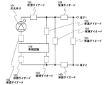
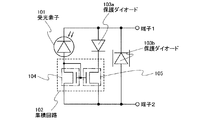
図1を用いて、本発明のフォトICの構成について説明する。図1は、本発明のフォトICの構成を示す回路図の一例であり、図1に示すフォトICは、フォトダイオードを用いた受光素子101と、受光素子101に光が照射されることにより、該受光素子101で生成された電流が与えられる集積回路102と、ダイオード、好ましくはフォトダイオードを用いた少なくとも1つの保護ダイオード103とを有する。図1では、複数の位置に保護ダイオード103が設けられているフォトICの回路図を示しているが、保護ダイオード103は、いずれかの位置に少なくとも1つ設けられていればよい。
(Embodiment 1)
The structure of the photo IC of the present invention will be described with reference to FIG. FIG. 1 is an example of a circuit diagram illustrating a configuration of a photo IC of the present invention. The photo IC illustrated in FIG. 1 includes a
集積回路102は1つまたは複数のトランジスタを有しており、受光素子101で生成された電流を増幅する、受光素子101で生成された電流を電圧に変換する、などの処理を行うことができる。
The
またフォトICは、少なくとも2つの端子1及び端子2を有している。そして、本発明のフォトICは、端子1と端子2とを結ぶ電流または電圧の経路において、保護ダイオード103が受光素子101または集積回路102と直列に接続されていても良いし、保護ダイオード103が受光素子101及び集積回路102と並列に接続されていても良い。
The photo IC has at least two
保護ダイオード103が有するアノードとカソードの向きは、受光素子101に光が照射されることで端子1と端子2の間に生じる電流または電圧が、保護ダイオード103によって小さくなるのを防ぐことができる方向、または、受光素子101に光が照射されていない状態において、保護ダイオード103を介して端子1と端子2の間に電流が流れるのを防ぐことができる方向に定めることが望ましい。具体的には、受光素子101と保護ダイオード103の接続関係を考慮して、保護ダイオード103が有するアノードとカソードの向きを定めるようにする。
The direction of the anode and the cathode of the
図2に、端子1と端子2とを結ぶ経路において、受光素子101と保護ダイオード103が直列に接続されている場合の、フォトICの回路図の一例を示す。図2では、複数の位置に保護ダイオード103が設けられているフォトICの回路図を示しているが、保護ダイオード103は、いずれかの位置に少なくとも1つ設けられていればよい。また図2に示すフォトICでは、受光素子101及び集積回路102が端子1と端子2の間に設けられている経路に加えて、受光素子101と集積回路102のうち集積回路102のみが端子1と端子2の間に設けられている経路を有している。集積回路102の構成によっては、必ずしも後者の経路をフォトICに設ける必要がない。
FIG. 2 shows an example of a circuit diagram of the photo IC when the
具体的に図2では、保護ダイオード103は、受光素子101及び集積回路102が端子1と端子2の間に設けられている経路において、端子1と受光素子101の間、受光素子101と集積回路102の間、集積回路102と端子2の間に設けることができる。そして、図2に示す各保護ダイオード103は、受光素子101とバイアス方向が逆になるように、すなわち、アノードとカソード間に生じる電圧の極性が逆になるように、アノードとカソードの向きを設定する。上記構成により、保護ダイオード103に光が照射されると、保護ダイオード103の順バイアス方向における抵抗値が低くなり、受光素子101に光が照射されることで端子1と端子2の間に生じる電流または電圧が、保護ダイオード103によって小さくなるのを防ぐことができる。
Specifically, in FIG. 2, the
次に図3に、受光素子101と集積回路102のうち、集積回路102のみが端子1と端子2の間に設けられている経路において、保護ダイオード103が受光素子101と並列になるように接続されている場合の、フォトICの回路図の一例を示す。図3では、複数の位置に保護ダイオード103が設けられているフォトICの回路図を示しているが、保護ダイオード103は、いずれかの位置に少なくとも1つ設けられていればよい。
Next, in FIG. 3, of the
具体的に図3では、保護ダイオード103は、受光素子101と集積回路102のうち、集積回路102のみが端子1と端子2の間に設けられている経路において、端子1と集積回路102の間、集積回路102と端子2の間に設けることができる。そして、図3に示す各保護ダイオード103は、受光素子101とバイアス方向が逆になるように、すなわち、アノードとカソード間に生じる電圧の極性が逆になるように、アノードとカソードの向きを設定する。上記構成により、保護ダイオード103に光が照射されると、保護ダイオード103の順バイアス方向における抵抗値が低くなる。なお、光の照射により受光素子101において電流が生成すると、受光素子101と集積回路102のうち、集積回路102のみが端子1と端子2の間に設けられている経路において、該電流に見合った大きさの電流または電圧が生じる。よって、保護ダイオード103の順バイアス方向における抵抗値が低くなると、受光素子101に光が照射されることで端子1と端子2の間に生じる電流または電圧が、保護ダイオード103によって小さくなるのを防ぐことができる。
Specifically, in FIG. 3, the
次に図4に、端子1と端子2とを結ぶ経路において、保護ダイオード103が受光素子101及び集積回路102と並列に接続されている場合の、フォトICの回路図の一例を示す。図4では、保護ダイオード103が1つだけ設けられているフォトICの回路図を示しているが、保護ダイオード103は必ずしも単数である必要はなく、少なくとも1つ設けられていればよい。また図4に示すフォトICでは、受光素子101及び集積回路102が端子1と端子2の間に設けられている経路に加えて、受光素子101と集積回路102のうち集積回路102のみが端子1と端子2の間に設けられている経路を有している。集積回路102の構成によっては、必ずしも後者の経路をフォトICに設ける必要がない。
Next, FIG. 4 shows an example of a circuit diagram of the photo IC when the
具体的に、図4に示す保護ダイオード103は、受光素子101とバイアス方向が同じになるように、すなわち、アノードとカソード間に生じる電圧の極性が同じになるように、アノードとカソードの向きを設定する。そして、受光素子101に光が照射されても、保護ダイオード103に該光が入射するのを防ぐことができる遮光膜を、保護ダイオード103に設ける。保護ダイオード103に光が入射するのを防ぐことで、受光素子101に光が照射しても保護ダイオード103の順バイアス方向における抵抗値は高いままなので、保護ダイオード103を介して端子1と端子2の間に電流が流れるのを防ぐことができる。
Specifically, the
次に図5に、端子1と端子2とを結ぶ経路において、複数の保護ダイオード103が受光素子101及び集積回路102と並列に接続されている場合の、フォトICの回路図の一例を示す。図5では保護ダイオード103を5つ設けている場合を例示しているが、保護ダイオード103はこれに限定されず、複数設けられていればよい。なお、図5に示すフォトICでは、受光素子101及び集積回路102が端子1と端子2の間に設けられている経路に加えて、受光素子101と集積回路102のうち集積回路102のみが端子1と端子2の間に設けられている経路を有している。集積回路102の構成によっては、必ずしも後者の経路をフォトICに設ける必要がない。
Next, FIG. 5 shows an example of a circuit diagram of a photo IC when a plurality of
具体的に、図5に示す複数の保護ダイオード103は、受光素子101とバイアス方向が逆になるように、すなわち、アノードとカソード間に生じる電圧の極性が逆になるように、アノードとカソードの向きを設定する。そして、受光素子101に光が照射されても、複数の保護ダイオード103に該光が入射するのを防ぐことができる遮光膜を、複数の保護ダイオード103に設ける。また、複数の保護ダイオード103は、端子1と端子2の間において全て直列になるように接続する。上記構成により、通常動作時において、複数の各保護ダイオード103に印加される電圧が小さくなるので、複数の保護ダイオード103を介して端子1と端子2の間に電流が流れるのを防ぐことができる。
Specifically, the plurality of
なお、本実施の形態では、保護ダイオード103の位置及び保護ダイオード103が有するアノードとカソードの向きが異なるフォトICの形態を、図2乃至図5にそれぞれ例示したが、図2乃至図5に示した形態をいずれか複数組み合わせて実施することも可能である。
Note that in this embodiment mode, photo ICs having different positions of the
本発明のフォトICは、保護ダイオード103として、受光素子101と同様に、縦型接合タイプのダイオード、好ましくはフォトダイオードを用いる。よって、保護ダイオード103を追加しても、フォトICの作製工程数が増えるのを防ぐことができる。また、縦型接合タイプのダイオードは、トランジスタを用いて形成されるダイオードに比べて広い接合面を確保することができる。よって、トランジスタよりも縦型接合タイプのダイオードの方が、サージ電流によって流れ込む電荷を接合面全体に分散させることで電界集中を防ぐことができるので、耐圧が高く、劣化或いは絶縁破壊されにくい。また、縦型接合タイプのダイオードは、各半導体膜の膜厚をトランジスタが有する半導体膜及びゲート絶縁膜よりも厚くすることができるので、サージ電流による劣化或いは絶縁破壊を防ぐことができる。
In the photo IC of the present invention, a vertical junction type diode, preferably a photodiode, is used as the
(実施の形態2)
本実施の形態では、図3と図4に示した形態を組み合わせた、フォトICの構成について説明する。
(Embodiment 2)
In this embodiment mode, a structure of a photo IC in which the modes illustrated in FIGS. 3 and 4 are combined will be described.
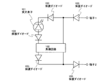
図6に示すフォトICは、フォトダイオードを用いた受光素子101と、受光素子101に光が照射されることにより、該受光素子101で生成された電流が与えられる集積回路102と、ダイオードまたはフォトダイオードを用いた少なくとも1つの保護ダイオード103aと、ダイオードまたはフォトダイオードを用いた少なくとも1つの保護ダイオード103bとを有する。
A photo IC shown in FIG. 6 includes a
なお図6では、トランジスタ104及びトランジスタ105を有する、カレントミラーを利用した増幅回路を、集積回路102の一例として示している。増幅回路は、受光素子101で生成された電流を増幅することができる。具体的に、トランジスタ104のゲートと、トランジスタ105のゲートは接続されている。また、トランジスタ104のソースまたはドレインのいずれか一方は、トランジスタ104のゲートと接続されている。そして、トランジスタ104は、端子1と端子2の間において、受光素子101と直列になるように接続されている。また、トランジスタ105は、端子1と端子2の間において、受光素子101と並列になるように接続されている。
Note that in FIG. 6, an amplifier circuit using a current mirror including the
上記増幅回路は、光の照射により受光素子101において生成した電流が、トランジスタ104のソースとドレイン間に流れると、トランジスタ105のソースとドレイン間にも電流が生じる。トランジスタ105のソースとドレイン間に生じる電流は、トランジスタ104のチャネル長とチャネル幅の比と、トランジスタ105のチャネル長とチャネル幅の比によって制御することができる。より好ましくは、トランジスタ104のチャネル幅と、トランジスタ105のチャネル幅の比でトランジスタ105のソースとドレイン間に生じる電流を制御する方が、該制御をより正確に行うことができるので、望ましい。
In the amplifier circuit, when a current generated in the
図6に示すフォトICは、少なくとも2つの端子1及び端子2を有している。そして、端子1と端子2とを結ぶ電流または電圧の経路において、受光素子101と集積回路102のうち、集積回路102のみが端子1と端子2の間に設けられている経路において、保護ダイオード103aは、受光素子101と並列になるように接続されている。具体的に保護ダイオード103aは、端子1とトランジスタ105の間において、受光素子101と並列になるように接続されている。なお、保護ダイオード103aは、端子2とトランジスタ105の間において、受光素子101と並列になるように接続されていても良い。また図6では、保護ダイオード103aが1つだけ設けられている場合を例示しているが、保護ダイオード103aは必ずしも単数である必要はなく、少なくとも1つ設けられていればよい。
The photo IC shown in FIG. 6 has at least two
そして、保護ダイオード103aは、受光素子101とバイアス方向が逆になるように、すなわち、アノードとカソード間に生じる電圧の極性が逆になるように、アノードとカソードの向きを設定する。上記構成により、保護ダイオード103aに光が照射されると、保護ダイオード103aの順バイアス方向における抵抗値が低くなる。保護ダイオード103aの順バイアス方向における抵抗値が低くなると、トランジスタ105のソースとドレイン間に流れる電流が、保護ダイオード103aによって小さくなるのを防ぐことができ、結果的に端子1と端子2の間に生じる電流が小さくなるのを防ぐことができる。
The
また、端子1と端子2とを結ぶ経路において、保護ダイオード103bは、受光素子101及び集積回路102と並列になるように接続されている。図6では、保護ダイオード103bが1つだけ設けられている場合を例示しているが、保護ダイオード103bは必ずしも単数である必要はなく、少なくとも1つ設けられていればよい。
Further, in the path connecting the
そして、保護ダイオード103bは、受光素子101とバイアス方向が同じになるように、すなわち、アノードとカソード間に生じる電圧の極性が同じになるように、アノードとカソードの向きを設定する。そして、受光素子101に光が照射されても、保護ダイオード103bに該光が入射するのを防ぐことができる遮光膜を、保護ダイオード103bに設ける。保護ダイオード103bに光が入射するのを防ぐことで、受光素子101に光が照射しても保護ダイオード103bの順バイアス方向における抵抗値は高いままなので、保護ダイオード103bを介して端子1と端子2の間に電流が流れるのを防ぐことができる。
The
なお、図6に示したフォトICは、保護ダイオード103bが、直接端子1と端子2の間に接続されているが、本発明はこの構成に限定されない。保護ダイオード103bと端子1の間、または保護ダイオード103bと端子2の間において、保護ダイオード103bと直列になるように、抵抗素子、ダイオード接続されたトランジスタなどを接続するようにしても良い。上記構成により、サージ電流によって集積回路102が破壊されるのを、より防ぐことができる。なおダイオード接続されたトランジスタとは、ゲートがソースまたはドレインのいずれか一方に接続された状態のトランジスタを意味する。
In the photo IC shown in FIG. 6, the
本発明のフォトICは、保護ダイオード103a、保護ダイオード103bとして、受光素子101と同様に、縦型接合タイプのフォトダイオードを用いることができる。よって、保護ダイオード103a、保護ダイオード103bを追加しても、フォトICの作製工程数が増えるのを防ぐことができる。また、縦型接合タイプのダイオードは、トランジスタを用いて形成されるダイオードに比べて広い接合面を確保することができる。よって、トランジスタよりも縦型接合タイプのダイオードの方が、サージ電流によって流れ込む電荷を接合面全体に分散させることで電界集中を防ぐことができるので、耐圧が高く、劣化或いは絶縁破壊されにくい。また、縦型接合タイプのダイオードは、各半導体膜の膜厚をトランジスタが有する半導体膜及びゲート絶縁膜よりも厚くすることができるので、サージ電流による劣化或いは絶縁破壊を防ぐことができる。
In the photo IC of the present invention, a vertical junction type photodiode can be used as the
そして図6に示したフォトICは、保護ダイオード103aと、保護ダイオード103bとを組み合わせることによって、保護ダイオード103aと、保護ダイオード103bとを単独で用いたフォトICに比べて、サージ電流により受光素子101、集積回路102、保護ダイオード103a及び保護ダイオード103bが破壊されるのを防ぐことができる。
The photo IC shown in FIG. 6 combines the
本実施の形態は、上記実施の形態と適宜組み合わせて実施することが可能である。 This embodiment can be implemented in combination with any of the above embodiments as appropriate.
(実施の形態3)
本実施の形態では、図2と図3に示した形態を組み合わせた、フォトICの構成について説明する。
(Embodiment 3)
In this embodiment, a structure of a photo IC in which the modes illustrated in FIGS. 2 and 3 are combined will be described.
図7に示すフォトICは、フォトダイオードを用いた受光素子101と、受光素子101に光が照射されることにより、該受光素子101で生成された電流が与えられる集積回路102と、ダイオードまたはフォトダイオードを用いた少なくとも1つの保護ダイオード103aと、ダイオードまたはフォトダイオードを用いた少なくとも1つの保護ダイオード103cとを有する。
A photo IC shown in FIG. 7 includes a
なお図7では、トランジスタ104及びトランジスタ105を有する、カレントミラーを利用した増幅回路を、集積回路102の一例として示している。
Note that in FIG. 7, an amplifier circuit including a
図7に示すフォトICは、少なくとも2つの端子1及び端子2を有している。そして、端子1と端子2とを結ぶ電流または電圧の経路において、受光素子101と集積回路102のうち、集積回路102のみが端子1と端子2の間に設けられている経路において、保護ダイオード103aは、受光素子101と並列になるように接続されている。具体的に保護ダイオード103aは、端子1とトランジスタ105の間において、受光素子101と並列になるように接続されている。なお、保護ダイオード103aは、端子2とトランジスタ105の間において、受光素子101と並列になるように接続されていても良い。また図7では、保護ダイオード103aが1つだけ設けられている場合を例示しているが、保護ダイオード103aは必ずしも単数である必要はなく、少なくとも1つ設けられていればよい。
The photo IC shown in FIG. 7 has at least two
そして、保護ダイオード103aは、受光素子101とバイアス方向が逆になるように、すなわち、アノードとカソード間に生じる電圧の極性が逆になるように、アノードとカソードの向きを設定する。上記構成により、保護ダイオード103aに光が照射されると、保護ダイオード103aの順バイアス方向における抵抗値が低くなる。保護ダイオード103aの順バイアス方向における抵抗値が低くなると、トランジスタ105のソースとドレイン間に流れる電流が、保護ダイオード103aによって小さくなるのを防ぐことができ、結果的に端子1と端子2の間に生じる電流が小さくなるのを防ぐことができる。
The
また、端子1と端子2とを結ぶ経路において、保護ダイオード103cは、受光素子101と直列になるように接続されている。具体的に図7では、保護ダイオード103cが、トランジスタ105と端子2の間に接続されている。保護ダイオード103cは、トランジスタ104と端子2の間に接続されていても良い。また、保護ダイオード103cは、受光素子101とトランジスタ104の間に接続されていても良い。また、保護ダイオード103cは、受光素子101と端子1の間に接続されていても良い。また、保護ダイオード103cは、トランジスタ105と端子1の間に接続されていても良い。なお、図7では、保護ダイオード103cが1つだけ設けられている場合を例示しているが、保護ダイオード103cは必ずしも単数である必要はなく、少なくとも1つ設けられていればよい。
In the path connecting the
そして、保護ダイオード103cは、受光素子101とバイアス方向が逆になるように、すなわち、アノードとカソード間に生じる電圧の極性が逆になるように、アノードとカソードの向きを設定する。上記構成により、保護ダイオード103cに光が照射されると、保護ダイオード103cの順バイアス方向における抵抗値が低くなる。保護ダイオード103cの順バイアス方向における抵抗値が低くなると、トランジスタ104のソースとドレイン間に流れる電流が、保護ダイオード103cによって小さくなるのを防ぐことができ、結果的に端子1と端子2の間に生じる電流が小さくなるのを防ぐことができる。
The
本発明のフォトICは、保護ダイオード103a、保護ダイオード103cとして、受光素子101と同様に、縦型接合タイプのダイオード、好ましくはフォトダイオードを用いる。縦型接合タイプのフォトダイオードを用いることによって、保護ダイオード103a、保護ダイオード103cを追加しても、フォトICの作製工程数が増えるのを防ぐことができる。また、縦型接合タイプのダイオードは、トランジスタを用いて形成されるダイオードに比べて広い接合面を確保することができる。よって、トランジスタよりも縦型接合タイプのダイオードの方が、サージ電流によって流れ込む電荷を接合面全体に分散させることで電界集中を防ぐことができるので、耐圧が高く、劣化或いは絶縁破壊されにくい。また、縦型接合タイプのダイオードは、各半導体膜の膜厚をトランジスタが有する半導体膜及びゲート絶縁膜よりも厚くすることができるので、サージ電流による劣化或いは絶縁破壊を防ぐことができる。
In the photo IC of the present invention, a vertical junction type diode, preferably a photodiode, is used as the
そして図7に示したフォトICは、保護ダイオード103aと、保護ダイオード103cとを組み合わせることによって、保護ダイオード103aと、保護ダイオード103cとを単独で用いたフォトICに比べて、サージ電流により受光素子101、集積回路102、保護ダイオード103a及び保護ダイオード103cが破壊されるのを防ぐことができる。
The photo IC shown in FIG. 7 combines the
本実施の形態は、上記実施の形態と適宜組み合わせて実施することが可能である。 This embodiment can be implemented in combination with any of the above embodiments as appropriate.
(実施の形態4)
本実施の形態では、図2と図3に示した形態を組み合わせた、フォトICの構成について説明する。
(Embodiment 4)
In this embodiment, a structure of a photo IC in which the modes illustrated in FIGS. 2 and 3 are combined will be described.
図8に示すフォトICは、フォトダイオードを用いた受光素子101と、受光素子101に光が照射されることにより、該受光素子101で生成された電流が与えられる集積回路102と、ダイオードまたはフォトダイオードを用いた少なくとも1つの保護ダイオード103aと、ダイオードまたはフォトダイオードを用いた少なくとも1つの保護ダイオード103bと、フォトダイオードを用いた少なくとも1つの保護ダイオード103cとを有する。
8 includes a
なお図8では、トランジスタ104及びトランジスタ105を有する、カレントミラーを利用した増幅回路を、集積回路102の一例として示している。
Note that in FIG. 8, an amplifier circuit using a current mirror including the
図8に示すフォトICは、少なくとも2つの端子1及び端子2を有している。そして、端子1と端子2とを結ぶ電流または電圧の経路において、受光素子101と集積回路102のうち、集積回路102のみが端子1と端子2の間に設けられている経路において、保護ダイオード103aは、受光素子101と並列になるように接続されている。具体的に保護ダイオード103aは、端子1とトランジスタ105の間において、受光素子101と並列になるように接続されている。なお、保護ダイオード103aは、端子2とトランジスタ105の間において、受光素子101と並列になるように接続されていても良い。また図8では、保護ダイオード103aが1つだけ設けられている場合を例示しているが、保護ダイオード103aは必ずしも単数である必要はなく、少なくとも1つ設けられていればよい。
The photo IC shown in FIG. 8 has at least two
そして、保護ダイオード103aは、受光素子101とバイアス方向が逆になるように、すなわち、アノードとカソード間に生じる電圧の極性が逆になるように、アノードとカソードの向きを設定する。上記構成により、保護ダイオード103aに光が照射されると、保護ダイオード103aの順バイアス方向における抵抗値が低くなる。保護ダイオード103aの順バイアス方向における抵抗値が低くなると、トランジスタ105のソースとドレイン間に流れる電流が、保護ダイオード103aによって小さくなるのを防ぐことができ、結果的に端子1と端子2の間に生じる電流が小さくなるのを防ぐことができる。
The
また、端子1と端子2とを結ぶ経路において、保護ダイオード103bは、受光素子101及び集積回路102と並列になるように接続されている。図8では、保護ダイオード103bが1つだけ設けられている場合を例示しているが、保護ダイオード103bは必ずしも単数である必要はなく、少なくとも1つ設けられていればよい。
Further, in the path connecting the
そして、保護ダイオード103bは、受光素子101とバイアス方向が同じになるように、すなわち、アノードとカソード間に生じる電圧の極性が同じになるように、アノードとカソードの向きを設定する。そして、受光素子101に光が照射されても、保護ダイオード103bに該光が入射するのを防ぐことができる遮光膜を、保護ダイオード103bに設ける。保護ダイオード103bに光が入射するのを防ぐことで、受光素子101に光が照射しても保護ダイオード103bの順バイアス方向における抵抗値は高いままなので、保護ダイオード103bを介して端子1と端子2の間に電流が流れるのを防ぐことができる。
The
また、端子1と端子2とを結ぶ経路において、保護ダイオード103cは、受光素子101と直列になるように接続されている。具体的に図8では、保護ダイオード103cが、トランジスタ105と端子2の間に接続されている。保護ダイオード103cは、トランジスタ104と端子2の間に接続されていても良い。また、保護ダイオード103cは、受光素子101とトランジスタ104の間に接続されていても良い。また、保護ダイオード103cは、受光素子101と端子1の間に接続されていても良い。また、保護ダイオード103cは、トランジスタ105と端子1の間に接続されていても良い。なお、図8では、保護ダイオード103cが1つだけ設けられている場合を例示しているが、保護ダイオード103cは必ずしも単数である必要はなく、少なくとも1つ設けられていればよい。
In the path connecting the
そして、保護ダイオード103cは、受光素子101とバイアス方向が逆になるように、すなわち、アノードとカソード間に生じる電圧の極性が逆になるように、アノードとカソードの向きを設定する。上記構成により、保護ダイオード103cに光が照射されると、保護ダイオード103cの順バイアス方向における抵抗値が低くなる。保護ダイオード103cの順バイアス方向における抵抗値が低くなると、トランジスタ104のソースとドレイン間に流れる電流が、保護ダイオード103cによって小さくなるのを防ぐことができ、結果的に端子1と端子2の間に生じる電流が小さくなるのを防ぐことができる。
The
本発明のフォトICは、保護ダイオード103a、保護ダイオード103b、保護ダイオード103cとして、受光素子101と同様に、縦型接合タイプのダイオード、好ましくはフォトダイオードを用いる。保護ダイオード103a、保護ダイオード103b、保護ダイオード103cとして、縦型接合タイプのフォトダイオードを用いることによって、保護ダイオード103a、保護ダイオード103b、保護ダイオード103cを追加しても、フォトICの作製工程数が増えるのを防ぐことができる。また、縦型接合タイプのダイオードは、トランジスタを用いて形成されるダイオードに比べて広い接合面を確保することができる。よって、トランジスタよりも縦型接合タイプのダイオードの方が、サージ電流によって流れ込む電荷を接合面全体に分散させることで電界集中を防ぐことができるので、耐圧が高く、劣化或いは絶縁破壊されにくい。また、縦型接合タイプのダイオードは、各半導体膜の膜厚をトランジスタが有する半導体膜及びゲート絶縁膜よりも厚くすることができるので、サージ電流による劣化或いは絶縁破壊を防ぐことができる。
In the photo IC of the present invention, a vertical junction type diode, preferably a photodiode, is used as the
そして図8に示したフォトICは、保護ダイオード103aと、保護ダイオード103bと、保護ダイオード103cとを組み合わせることによって、保護ダイオード103aと、保護ダイオード103bと、保護ダイオード103cとを単独で用いたフォトICに比べて、また、保護ダイオード103aと、保護ダイオード103bと、保護ダイオード103cとのいずれか2つを組み合わせたフォトICに比べて、サージ電流により受光素子101、集積回路102、保護ダイオード103a、保護ダイオード103b及び保護ダイオード103cが破壊されるのを防ぐことができる。
The photo IC shown in FIG. 8 is a photo IC using the
本実施の形態は、上記実施の形態と適宜組み合わせて実施することが可能である。 This embodiment can be implemented in combination with any of the above embodiments as appropriate.
(実施の形態5)
本実施の形態では、集積回路として増幅回路を用いた本発明のフォトICの、具体的な構成について説明する。
(Embodiment 5)
In this embodiment mode, a specific structure of a photo IC of the present invention using an amplifier circuit as an integrated circuit will be described.
図9に、本実施の形態のフォトICの回路図を示す。また、図9に示したフォトICの上面図の一例を、図10に示す。 FIG. 9 shows a circuit diagram of the photo IC of this embodiment mode. FIG. 10 shows an example of a top view of the photo IC shown in FIG.
端子1と端子2とを結ぶ経路において、保護ダイオード106〜110は、受光素子101及び集積回路102と並列に接続されている。なお、図9及び図10では5つの保護ダイオード106〜110を設けている場合を例示しているが、保護ダイオードの数はこれに限定されず、複数設けられていればよい。また、図9及び図10では、トランジスタ104及びトランジスタ105を有する、カレントミラーを利用した増幅回路を、集積回路102の一例として示している。
In the path connecting the
また、図9及び図10に示す保護ダイオード106〜110は、受光素子101とバイアス方向が逆になるように、すなわち、アノードとカソード間に生じる電圧の極性が逆になるように、アノードとカソードの向きを設定する。また、保護ダイオード106〜110は、端子1と端子2の間において全て直列になるように接続されている。そして、受光素子101に光が照射されても、保護ダイオード106〜110に該光が入射するのを防ぐことができる遮光膜を、保護ダイオード106〜110に設ける。
Further, the
上記構成により、通常動作時において、保護ダイオード106〜110のそれぞれに印加される電圧が小さくなるので、保護ダイオード106〜110を介して端子1と端子2の間に電流が流れるのを防ぐことができる。
With the above configuration, during normal operation, the voltage applied to each of the
そして、図10に示すように、本発明のフォトICは、半導体膜が積層された縦型接合タイプのダイオード、好ましくはフォトダイオードを、受光素子101、保護ダイオード106〜110として用いている。
As shown in FIG. 10, the photo IC of the present invention uses a vertical junction type diode in which semiconductor films are stacked, preferably a photodiode, as the
具体的に、受光素子101のアノードは、導電膜201に接続されている。導電膜201は、導電膜202に接続されており、導電膜202は、その一部がトランジスタ104のゲート及びトランジスタ105のゲートとして機能している。また、導電膜202は導電膜203に接続されており、導電膜203はトランジスタ104のソースまたはドレインの一方に接続されている。導電膜204は、トランジスタ104のソースまたはドレインの他方と、トランジスタ105のソースまたはドレインの一方と接続されている。
Specifically, the anode of the
また、導電膜204は、導電膜205に接続されており、導電膜205は領域206において端子2に接続される。そして、導電膜205は、保護ダイオード110のカソードに接続され、保護ダイオード110のアノードは導電膜207に接続されている。導電膜207は導電膜208に接続されており、導電膜208は、保護ダイオード109のカソードに接続されている。保護ダイオード109のアノードは導電膜209に接続されており、導電膜209は導電膜210に接続されている。導電膜210は、保護ダイオード108のカソードに接続されており、保護ダイオード108のアノードは導電膜211に接続されている。導電膜211は導電膜212に接続されており、導電膜212は保護ダイオード107のカソードに接続されている。保護ダイオード107のアノードは、導電膜213に接続されており、導電膜213は導電膜214に接続されている。導電膜214は保護ダイオード106のカソードに接続されており、保護ダイオード106のアノードは、導電膜215に接続されている。
In addition, the
本実施の形態では、導電膜207が、保護ダイオード110のアノードにも接続され、アノードと重なるように形成されており、光が保護ダイオード110のアノードに入射しないようにするための遮光膜として機能している。また、同様に導電膜209が、保護ダイオード109の遮光膜として機能している。また、同様に導電膜211が、保護ダイオード108の遮光膜として機能している。また、同様に導電膜213が、保護ダイオード107の遮光膜として機能している。また、同様に導電膜215が、保護ダイオード106の遮光膜として機能している。
In the present embodiment, the
なお、本実施の形態では、保護ダイオード106〜110を、アノード側から遮光しているが、本発明はこの構成に限定されない。保護ダイオードが、アノード側とカソード側の少なくとも一方から入射する光を遮光するための遮光膜を、有していても良い。また、本実施の形態では、素子または端子どうしを電気的に接続させるための導電膜を遮光膜として用いているが、本発明はこの構成に限定されない。素子または端子どうしを電気的に接続させるための導電膜とは異なる遮光膜を、個別に形成しても良い。
In the present embodiment, the
導電膜215は、トランジスタ105のソースまたはドレインの他方と接続されている。また、導電膜215は導電膜216に接続されており、導電膜216は領域217において端子1に接続される。そして、導電膜216は、受光素子101のカソードと接続されている。
The
なお、導電膜201、導電膜203、導電膜204、導電膜207、導電膜209、導電膜211、導電膜213、導電膜215は、1つの絶縁膜上に形成された導電膜を所望の形状に加工(パターニング)することで、形成することができる。また、導電膜205、導電膜208、導電膜210、導電膜212、導電膜214、導電膜216は、1つの絶縁膜上に形成された導電膜を所望の形状に加工(パターニング)することで、形成することができる。
Note that the
また、本発明では、保護ダイオード106〜110として、受光素子101と同様に、縦型接合タイプのフォトダイオードを用いることで、保護ダイオード106〜110を追加しても、フォトICの作製工程数が増えるのを防ぐことができる。また、縦型接合タイプのダイオードは、トランジスタを用いて形成されるダイオードに比べて広い接合面を確保することができる。よって、トランジスタよりも縦型接合タイプのダイオードの方が、サージ電流によって流れ込む電荷を接合面全体に分散させることで電界集中を防ぐことができるので、耐圧が高く、劣化或いは絶縁破壊されにくい。また、縦型接合タイプのダイオードは、各半導体膜の膜厚を集積回路102に含まれるトランジスタが有する各半導体膜の膜厚やゲート絶縁膜よりも厚くすることができるので、サージ電流による劣化或いは絶縁破壊を防ぐことができる。
Further, in the present invention, as the
本実施の形態は、上記実施の形態と適宜組み合わせて実施することが可能である。 This embodiment can be implemented in combination with any of the above embodiments as appropriate.
(実施の形態6)
次に、本発明のフォトICの作製方法について詳しく述べる。なお、本実施の形態では、薄膜トランジスタ(TFT)と、縦型接合タイプのPINフォトダイオードとを半導体素子の一例として示すが、本発明のフォトICに用いられる半導体素子はこれらに限定されない。例えばTFT及びPINフォトダイオードの他に、記憶素子、抵抗、ダイオード、容量、インダクタなどを用いることができる。また、本発明のフォトICは、縦型接合タイプのPINフォトダイオードの代わりに、縦型接合タイプのPNフォトダイオードを用いていても良い。
(Embodiment 6)
Next, a method for manufacturing the photo IC of the present invention will be described in detail. Note that in this embodiment mode, a thin film transistor (TFT) and a vertical junction type PIN photodiode are shown as an example of a semiconductor element; however, the semiconductor element used in the photo IC of the present invention is not limited thereto. For example, a memory element, a resistor, a diode, a capacitor, an inductor, or the like can be used in addition to the TFT and the PIN photodiode. The photo IC of the present invention may use a vertical junction type PN photodiode instead of the vertical junction type PIN photodiode.
まず図11(A)に示すように、透光性を有する基板400上に、絶縁膜401、半導体膜402を順に形成する。絶縁膜401及び半導体膜402は、大気に触れることなく連続して形成することが可能である。
First, as illustrated in FIG. 11A, an insulating
基板400として、例えばバリウムホウケイ酸ガラスや、アルミノホウケイ酸ガラスなどのガラス基板、石英基板等を用いることができる。プラスチック等の合成樹脂を含む、可撓性を有する基板は、一般的に上記基板と比較して耐熱温度が低い傾向にあるが、作製工程における処理温度に耐え得るのであれば用いることが可能である。本実施の形態では、基板400として、厚さ0.5mmの、無アルカリガラスであるアルミノ珪酸塩ガラス基板(旭硝子社製 商品名AN100)を用いる。
As the
絶縁膜401は基板400中に含まれるNaなどのアルカリ金属やアルカリ土類金属が、半導体膜402中に拡散し、トランジスタなどの半導体素子の特性に悪影響を及ぼすのを防ぐために設ける。よってアルカリ金属やアルカリ土類金属の半導体膜402への拡散を抑えることができるバリア性の高い絶縁材料を用いて、絶縁膜401を形成するのが望ましい。なお、ガラス基板またはプラスチック基板のように、アルカリ金属やアルカリ土類金属が多少なりとも含まれている基板を用いる場合、不純物の拡散を防ぐという観点から基板400と半導体膜402との間に絶縁膜401を設けることは有効である。しかし、石英基板など不純物の拡散がさして問題とならない基板400を用いる場合は、必ずしも設ける必要はない。
The insulating
絶縁膜401は、CVD法やスパッタリング法等を用いて、酸化珪素、窒化珪素、酸化窒化珪素、窒化酸化珪素、窒化アルミニウム等の絶縁性を有する材料を用いて形成する。
The insulating
なお、酸化窒化珪素膜とは、その組成として、窒素よりも酸素の含有量が多い膜であって、ラザフォード後方散乱法(RBS:Rutherford Backscattering Spectrometry)及び水素前方散乱法(HFS:Hydrogen Forward Scattering)を用いて測定した場合に、濃度範囲として酸素が50〜70原子%、窒素が0.5〜15原子%、珪素が25〜35原子%、水素が0.1〜10原子%の範囲で含まれる膜をいう。また、窒化酸化珪素膜とは、その組成として、酸素よりも窒素の含有量が多い膜であって、RBS及びHFSを用いて測定した場合に、濃度範囲として酸素が5〜30原子%、窒素が20〜55原子%、珪素が25〜35原子%、水素が10〜25原子%の範囲で含まれる膜をいう。但し、酸化窒化珪素または窒化酸化珪素を構成する原子の合計を100原子%としたとき、窒素、酸素、珪素及び水素の含有比率が上記の範囲内に含まれるものとする。 Note that the silicon oxynitride film is a film having a higher oxygen content than nitrogen as a composition, and is Rutherford Backscattering Spectroscopy (RBS) and Hydrogen Forward Scattering (HFS). As a concentration range, oxygen is included in the range of 50 to 70 atomic%, nitrogen is 0.5 to 15 atomic%, silicon is 25 to 35 atomic%, and hydrogen is 0.1 to 10 atomic%. Refers to a membrane. A silicon nitride oxide film is a film having a nitrogen content higher than that of oxygen as a composition. When measured using RBS and HFS, the concentration range of oxygen is 5 to 30 atomic%, nitrogen. Is a film containing 20 to 55 atomic%, silicon is 25 to 35 atomic%, and hydrogen is 10 to 25 atomic%. However, when the total number of atoms constituting silicon oxynitride or silicon nitride oxide is 100 atomic%, the content ratio of nitrogen, oxygen, silicon, and hydrogen is included in the above range.
絶縁膜401は、単数の絶縁膜を用いたものであっても、複数の絶縁膜を積層して用いたものであっても良い。本実施の形態では、膜厚50nmの窒化酸化珪素膜、膜厚140nmの酸化窒化珪素膜を順に積層して絶縁膜401を形成するが、各膜の材質、膜厚、積層数は、これに限定されるものではない。
The insulating
酸化珪素膜は、シランと酸素、TEOS(テトラエトキシシラン)と酸素等の組み合わせの混合ガスを用い、熱CVD、プラズマCVD、常圧CVD、バイアスECRCVD等の方法によって形成することができる。また、窒化珪素膜は、代表的には、シランとアンモニアの混合ガスを用い、プラズマCVDによって形成することができる。また、酸化窒化珪素膜、窒化酸化珪素膜は、代表的には、シランと一酸化二窒素の混合ガスを用い、プラズマCVDによって形成することができる。 The silicon oxide film can be formed by a method such as thermal CVD, plasma CVD, atmospheric pressure CVD, or bias ECRCVD, using a mixed gas of a combination of silane and oxygen, TEOS (tetraethoxysilane), and oxygen. The silicon nitride film can be typically formed by plasma CVD using a mixed gas of silane and ammonia. The silicon oxynitride film and the silicon nitride oxide film can be typically formed by plasma CVD using a mixed gas of silane and dinitrogen monoxide.
半導体膜402は、絶縁膜401を形成した後、大気に曝さずに形成することが望ましい。半導体膜402の膜厚は20〜200nm(望ましくは40〜170nm、好ましくは50〜150nm)とする。なお、半導体膜402は、非晶質半導体、多結晶半導体、微結晶(セミアモルファス若しくはマイクロクリスタル)半導体などを用いることができる。半導体膜402は、スパッタ法、LPCVD法、またはプラズマCVD法等により形成することができる。
The
または、半導体膜402として、単結晶半導体を用いた透光性のSOI構造を有する基板などを用いてトランジスタを形成してもよい。これらにより、特性やサイズや形状などのバラツキが少なく、電流供給能力が高く、サイズの小さいトランジスタを製造することができる。これらのトランジスタを用いると、回路の低消費電力化、又は回路の高集積化を図ることができる。
Alternatively, as the
また、半導体膜402に用いられる半導体の材料として、シリコン(Si)、ゲルマニウム(Ge)などの単体のほかGaAs、InP、SiC、ZnSe、GaN、SiGeなどのような化合物半導体も用いることができる。また酸化物半導体である酸化亜鉛(ZnO)、酸化スズ(SnO2)なども用いることができ、ZnOを半導体膜に用いる場合、ゲート絶縁膜としてY2O3、Al2O3、TiO2、それらの積層などを用いると良く、ゲート電極、半導体膜402に接する導電膜として、ITO、Au、Tiなどを用いるとよい。
As a semiconductor material used for the
非晶質半導体膜は、例えば半導体として珪素を用いる場合、珪素を含む気体をグロー放電分解することにより形成することができる。珪素を含む気体としては、SiH4、Si2H6が挙げられる。この珪素を含む気体を、水素、水素及びヘリウムで希釈して用いても良い。 For example, when silicon is used as a semiconductor, the amorphous semiconductor film can be formed by glow discharge decomposition of a gas containing silicon. Examples of the gas containing silicon include SiH 4 and Si 2 H 6 . The gas containing silicon may be diluted with hydrogen, hydrogen, and helium.
微結晶半導体は、ギブスの自由エネルギーを考慮すれば非晶質と単結晶の中間的な準安定状態に属するものである。すなわち、自由エネルギー的に安定な第3の状態を有する半導体であって、短距離秩序を持ち格子歪みを有する。柱状または針状結晶が基板表面に対して法線方向に成長している。微結晶半導体の代表例である微結晶シリコンは、そのラマンスペクトルが単結晶シリコンを示す520cm−1よりも低波数側に、シフトしている。即ち、単結晶シリコンを示す520cm−1とアモルファスシリコンを示す480cm−1の間に微結晶シリコンのラマンスペクトルのピークがある。また、未結合手(ダングリングボンド)を終端するため水素またはハロゲンを少なくとも1原子%またはそれ以上含ませている。さらに、ヘリウム、アルゴン、クリプトン、ネオンなどの希ガス元素を含ませて格子歪みをさらに助長させることで、安定性が増し良好な微結晶半導体膜が得られる。 A microcrystalline semiconductor belongs to a metastable state between an amorphous state and a single crystal state in consideration of Gibbs free energy. That is, it is a semiconductor having a third state that is stable in terms of free energy, and has a short-range order and lattice distortion. Columnar or needle-like crystals grow in the normal direction with respect to the substrate surface. Microcrystalline silicon which is a typical example of a microcrystalline semiconductor has a Raman spectrum shifted to a lower wave number side than 520 cm −1 indicating single crystal silicon. That is, the peak of the Raman spectrum of microcrystalline silicon is between 520 cm −1 indicating single crystal silicon and 480 cm −1 indicating amorphous silicon. In addition, at least 1 atomic% or more of hydrogen or halogen is contained to terminate dangling bonds (dangling bonds). Further, by adding a rare gas element such as helium, argon, krypton, or neon to further promote lattice distortion, stability can be improved and a good microcrystalline semiconductor film can be obtained.
この微結晶半導体膜は、周波数が数十MHz〜数百MHzの高周波プラズマCVD法、または周波数が1GHz以上のマイクロ波プラズマCVD装置により形成することができる。代表的には、SiH4、Si2H6、SiH2Cl2、SiHCl3、SiCl4、SiF4などの珪素を含む化合物を水素で希釈して用いることで、微結晶半導体膜を形成することができる。また、珪素を含む化合物及び水素に加え、ヘリウム、アルゴン、クリプトン、ネオンから選ばれた一種または複数種の希ガス元素で希釈して微結晶半導体膜を形成することができる。これらのときの珪化水素などの珪素を含む化合物に対して、水素の流量比を5倍以上200倍以下、好ましくは50倍以上150倍以下、更に好ましくは100倍とする。 This microcrystalline semiconductor film can be formed by a high-frequency plasma CVD method with a frequency of several tens to several hundreds of MHz or a microwave plasma CVD apparatus with a frequency of 1 GHz or more. Typically, a microcrystalline semiconductor film is formed by using a silicon-containing compound such as SiH 4 , Si 2 H 6 , SiH 2 Cl 2 , SiHCl 3 , SiCl 4 , and SiF 4 diluted with hydrogen. Can do. In addition to the compound containing silicon and hydrogen, the microcrystalline semiconductor film can be formed by dilution with one or more kinds of rare gas elements selected from helium, argon, krypton, and neon. At this time, the hydrogen flow rate ratio is 5 to 200 times, preferably 50 to 150 times, and more preferably 100 times to the compound containing silicon such as hydrogen silicide.
多結晶半導体を用いた半導体膜402は、非晶質半導体膜または微結晶半導体膜を、レーザ結晶化法、熱結晶化法、またはニッケルなどの結晶化を助長する触媒元素を用いた熱結晶化法等を単独で、或いは複数組み合わせて実施することで、形成することができる。また、多結晶半導体を、スパッタ法、プラズマCVD法、熱CVD法などを用いて、直接形成しても良い。また、プラズマ法を用いて、多結晶半導体を選択的に基板に形成してもよい。結晶化を助長する触媒元素を導入せずにレーザ結晶化を行う場合は、レーザ光の照射により非晶半導体膜が飛散する現象(アブレーション)が生じるのを防ぐために、非晶半導体膜にレーザ光を照射する前に、窒素雰囲気下500℃で1時間加熱し、非晶半導体膜が含有する水素濃度を1×10²⁰atoms/cm3以下とすると良い。
As the
例えばレーザ結晶化を用いて多結晶半導体膜を形成する場合、レーザ結晶化の前に、レーザに対する半導体膜402の耐性を高めるために、550℃、4時間の加熱処理を該半導体膜402に対して行なう。そして連続発振が可能な固体レーザを用い、基本波の第2高調波〜第4高調波のレーザ光を照射することで、大粒径の結晶を得ることができる。例えば、代表的には、Nd:YVO4レーザ(基本波1064nm)の第2高調波(532nm)や第3高調波(355nm)を用いるのが望ましい。具体的には、連続発振のYVO4レーザから射出されたレーザ光を非線形光学素子により高調波に変換し、出力10Wのレーザ光を得る。そして、好ましくは光学系により照射面にて矩形状または楕円形状のレーザ光に成形して、半導体膜402に照射する。このときのパワー密度は0.01〜100MW/cm2程度(好ましくは0.1〜10MW/cm2)が必要である。そして、走査速度を10〜2000cm/sec程度とし、照射する。
For example, in the case of forming a polycrystalline semiconductor film using laser crystallization, a heat treatment at 550 ° C. for 4 hours is performed on the
連続発振の気体レーザとして、Arレーザ、Krレーザなどを用いることが出来る。また連続発振の固体レーザとして、YAGレーザ、YVO4レーザ、YLFレーザ、YAlO3レーザ、フォルステライト(Mg2SiO4)レーザ、GdVO4レーザ、Y2O3レーザ、ガラスレーザ、ルビーレーザ、アレキサンドライトレーザ、Ti:サファイアレーザなどを用いることが出来る。 As a continuous wave gas laser, an Ar laser, a Kr laser, or the like can be used. As continuous wave solid-state lasers, YAG laser, YVO 4 laser, YLF laser, YAlO 3 laser, forsterite (Mg 2 SiO 4 ) laser, GdVO 4 laser, Y 2 O 3 laser, glass laser, ruby laser, alexandrite laser Ti: sapphire laser or the like can be used.
またパルス発振のレーザとして、例えばArレーザ、Krレーザ、エキシマレーザ、CO2レーザ、YAGレーザ、Y2O3レーザ、YVO4レーザ、YLFレーザ、YAlO3レーザ、ガラスレーザ、ルビーレーザ、アレキサンドライトレーザ、Ti:サファイアレーザ、銅蒸気レーザまたは金蒸気レーザを用いることができる。 As pulse oscillation lasers, for example, Ar laser, Kr laser, excimer laser, CO 2 laser, YAG laser, Y 2 O 3 laser, YVO 4 laser, YLF laser, YAlO 3 laser, glass laser, ruby laser, alexandrite laser, A Ti: sapphire laser, a copper vapor laser, or a gold vapor laser can be used.
また、パルス発振のレーザ光の発振周波数を10MHz以上とし、通常用いられている数十Hz〜数百Hzの周波数帯よりも著しく高い周波数帯を用いてレーザ結晶化を行なっても良い。パルス発振でレーザ光を半導体膜402に照射してから半導体膜402が完全に固化するまでの時間は数十nsec〜数百nsecと言われている。よって上記周波数を用いることで、半導体膜402がレーザ光によって溶融してから固化するまでに、次のパルスのレーザ光を照射できる。したがって、半導体膜402中において固液界面を連続的に移動させることができるので、走査方向に向かって連続的に成長した結晶粒を有する半導体膜402が形成される。具体的には、含まれる結晶粒の走査方向における幅が10〜30μm、走査方向に対して垂直な方向における幅が1〜5μm程度の結晶粒の集合を形成することができる。該走査方向に沿って連続的に成長した単結晶の結晶粒を形成することで、少なくともTFTのチャネル方向には結晶粒界のほとんど存在しない半導体膜402の形成が可能となる。
Alternatively, laser crystallization may be performed using a frequency band that is significantly higher than a frequency band of several tens to several hundreds Hz that is normally used, with an oscillation frequency of pulsed laser light of 10 MHz or higher. It is said that the time from when the
なおレーザ結晶化は、連続発振の基本波のレーザ光と連続発振の高調波のレーザ光とを並行して照射するようにしても良いし、連続発振の基本波のレーザ光とパルス発振の高調波のレーザ光とを並行して照射するようにしても良い。 Laser crystallization may be performed by irradiating a continuous-wave fundamental laser beam and a continuous-wave harmonic laser beam in parallel, or a continuous-wave fundamental laser beam and a pulse oscillation harmonic. You may make it irradiate with the laser beam of a wave in parallel.
なお、希ガスや窒素などの不活性ガス雰囲気中でレーザ光を照射するようにしても良い。これにより、レーザ光照射による半導体表面の荒れを抑えることができ、界面準位密度のばらつきによって生じる閾値のばらつきを抑えることができる。 Note that laser light may be irradiated in an inert gas atmosphere such as a rare gas or nitrogen. Thereby, roughness of the semiconductor surface due to laser light irradiation can be suppressed, and variation in threshold value caused by variation in interface state density can be suppressed.
結晶化を助長する触媒元素を用いた熱結晶化法を用いる場合、非晶質半導体膜への触媒元素の導入の仕方としては、当該触媒元素を非晶質半導体膜の表面又はその内部に存在させ得る手法であれば特に限定はなく、例えばスパッタ法、CVD法、プラズマ処理法(プラズマCVD法も含む)、吸着法、金属塩の溶液を塗布する方法を使用することができる。このうち溶液を用いる方法は簡便であり、触媒元素の濃度調整が容易である。また、このとき非晶質半導体膜の表面の濡れ性を改善し、非晶質半導体膜の表面全体に水溶液を行き渡らせるため、酸素雰囲気中でのUV光の照射、熱酸化法、ヒドロキシラジカルを含むオゾン水又は過酸化水素による処理等により、非晶質半導体膜の表面に酸化膜を形成することが望ましい。 When a thermal crystallization method using a catalytic element that promotes crystallization is used, the catalytic element is introduced into the amorphous semiconductor film either on the surface of the amorphous semiconductor film or inside thereof. For example, a sputtering method, a CVD method, a plasma treatment method (including a plasma CVD method), an adsorption method, or a method of applying a metal salt solution can be used. Among these, the method using a solution is simple and the concentration of the catalyst element can be easily adjusted. At this time, in order to improve the wettability of the surface of the amorphous semiconductor film and to spread the aqueous solution over the entire surface of the amorphous semiconductor film, irradiation with UV light in an oxygen atmosphere, thermal oxidation method, hydroxy radical It is desirable to form an oxide film on the surface of the amorphous semiconductor film by treatment with ozone water or hydrogen peroxide.
そして、非晶質半導体膜へ触媒元素を導入した後、加熱処理(550℃〜750℃で3分〜24時間)を行うことにより、多結晶半導体膜を形成することができる。結晶化を助長(促進)する触媒元素としては、鉄(Fe)、ニッケル(Ni)、コバルト(Co)、ルテニウム(Ru)、ロジウム(Rh)、パラジウム(Pd)、オスミウム(Os)、イリジウム(Ir)、白金(Pt)、銅(Cu)及び金(Au)から選ばれた一種又は複数種類を用いることができる。 Then, after introducing the catalyst element into the amorphous semiconductor film, a polycrystalline semiconductor film can be formed by performing heat treatment (at 550 ° C. to 750 ° C. for 3 minutes to 24 hours). Catalyst elements that promote (promote) crystallization include iron (Fe), nickel (Ni), cobalt (Co), ruthenium (Ru), rhodium (Rh), palladium (Pd), osmium (Os), iridium ( One or more kinds selected from Ir), platinum (Pt), copper (Cu), and gold (Au) can be used.
上記結晶化を行った後、多結晶半導体膜から結晶化を助長する触媒元素を除去し、当該触媒元素の濃度を低減させるため、不純物元素を含む半導体膜を多結晶半導体に接するように形成する。上記不純物元素を含む半導体膜は、ゲッタリングシンクとして機能する。不純物元素として、N型を付与する不純物元素、P型を付与する不純物元素や希ガス元素などを用いることができ、例えばリン(P)、窒素(N)、ヒ素(As)、アンチモン(Sb)、ビスマス(Bi)、ボロン(B)、ヘリウム(He)、ネオン(Ne)、アルゴン(Ar)、Kr(クリプトン)、Xe(キセノン)から選ばれた一種または複数種を用いることができる。そして、希ガス元素を含む半導体膜を、結晶化を助長する触媒元素を含む多結晶半導体膜に接するように形成し、加熱処理(550℃〜750℃で3分〜24時間)を行う。上記加熱処理により、多結晶半導体膜中に含まれる結晶化を助長する触媒元素は、希ガス元素を含む半導体膜中に移動し、多結晶半導体膜中の結晶化を助長する触媒元素の濃度は低減する。その後、ゲッタリングシンクとなった希ガス元素を含む半導体膜を除去する。 After performing the crystallization, a catalyst film that promotes crystallization is removed from the polycrystalline semiconductor film, and a semiconductor film containing an impurity element is formed in contact with the polycrystalline semiconductor in order to reduce the concentration of the catalyst element. . The semiconductor film containing the impurity element functions as a gettering sink. As the impurity element, an impurity element imparting N-type, an impurity element imparting P-type, a rare gas element, or the like can be used. For example, phosphorus (P), nitrogen (N), arsenic (As), antimony (Sb) , Bismuth (Bi), boron (B), helium (He), neon (Ne), argon (Ar), Kr (krypton), or Xe (xenon) can be used. Then, a semiconductor film containing a rare gas element is formed so as to be in contact with the polycrystalline semiconductor film containing a catalytic element that promotes crystallization, and heat treatment (at 550 ° C. to 750 ° C. for 3 minutes to 24 hours) is performed. Through the heat treatment, the catalyst element that promotes crystallization contained in the polycrystalline semiconductor film moves into the semiconductor film containing a rare gas element, and the concentration of the catalyst element that promotes crystallization in the polycrystalline semiconductor film is To reduce. After that, the semiconductor film containing a rare gas element that has become a gettering sink is removed.
本実施の形態では、触媒元素を用いた結晶化方法と、レーザ結晶化法とを組み合わせて、多結晶珪素を用いた半導体膜402を形成する。以下、本実施の形態における具体的な半導体膜402の作製方法について説明する。
In this embodiment mode, the
本実施の形態では、まず、膜厚50nmの非晶質珪素膜を絶縁膜401上に形成した後、重量換算で10ppmのニッケルを含む酢酸ニッケル溶液を、非晶質珪素膜にスピナーで塗布する。なお、溶液を用いて触媒元素を添加する方法に代えて、スパッタ法でニッケル元素を全面に散布する方法を用いてもよい。次に、加熱処理(500℃、1時間)の後、結晶化のための加熱処理(550℃、4時間)を行って、非晶質珪素膜を結晶化させることで、多結晶珪素を有する半導体膜402を形成する。
In this embodiment, first, an amorphous silicon film with a thickness of 50 nm is formed over the insulating
次に、多結晶珪素を有する半導体膜402の表面に形成された酸化膜を、希フッ酸等で除去する。その後、結晶化率を高め、結晶粒内に残される欠陥を補修するためのレーザ光(XeCl:波長308nm)の照射を大気中、または酸素雰囲気中で行う。
Next, the oxide film formed on the surface of the
レーザ光には波長400nm以下のエキシマレーザ光や、YAGレーザの第2高調波又は第3高調波を用いる。ここでは、繰り返し周波数10〜1000Hz程度のパルスレーザ光を用い、当該レーザ光を光学系にて100〜500mJ/cm2に集光し、90〜95%のオーバーラップ率をもって照射し、シリコン膜表面を走査させればよい。本実施の形態では、繰り返し周波数30Hz、パワー密度470mJ/cm2でレーザ光の照射を大気中で行なう。 As the laser light, excimer laser light having a wavelength of 400 nm or less, or the second harmonic or the third harmonic of a YAG laser is used. Here, a pulsed laser beam having a repetition frequency of about 10 to 1000 Hz is used, the laser beam is condensed to 100 to 500 mJ / cm 2 by an optical system, and irradiated with an overlap rate of 90 to 95%. May be scanned. In this embodiment mode, laser light irradiation is performed in the atmosphere at a repetition frequency of 30 Hz and a power density of 470 mJ / cm 2 .
なお、上記レーザ光の照射は、大気中、または酸素雰囲気中で行うため、レーザ光の照射により表面に酸化膜が形成される。なお、本実施の形態ではパルスレーザを用いた例を示したが、連続発振のレーザを用いてもよく、半導体膜の結晶化に際し、大粒径の結晶を得るためには、連続発振が可能な固体レーザを用い基本波の第2高調波〜第4高調波を適用するのが好ましい。代表的には、Nd:YVO4レーザ(基本波1064nm)の第2高調波(532nm)や第3高調波(355nm)を適用すればよい。 Note that since the laser light irradiation is performed in the air or an oxygen atmosphere, an oxide film is formed on the surface by the laser light irradiation. Note that although an example using a pulse laser is shown in this embodiment mode, a continuous wave laser may be used, and continuous oscillation is possible in order to obtain a crystal with a large grain size when a semiconductor film is crystallized. It is preferable to apply the second to fourth harmonics of the fundamental wave using a simple solid-state laser. Typically, a second harmonic (532 nm) or a third harmonic (355 nm) of an Nd: YVO 4 laser (fundamental wave 1064 nm) may be applied.
連続発振のレーザを用いる場合には、出力10Wの連続発振のYVO4レーザから射出されたレーザ光を非線形光学素子により高調波に変換する。また、共振器の中にYVO4結晶と非線形光学素子を入れて、高調波を射出する方法もある。そして、好ましくは光学系により照射面にて矩形状または楕円形状のレーザ光に成形して、被処理体に照射する。このときのパワー密度は0.01〜100MW/cm2程度(好ましくは0.1〜10MW/cm2)が必要である。そして、10〜2000cm/s程度の速度でレーザ光に対して相対的に半導体膜を移動させて照射すればよい。 In the case of using a continuous wave laser, laser light emitted from a continuous wave YVO 4 laser having an output of 10 W is converted into a harmonic by a non-linear optical element. There is also a method of emitting harmonics by putting a YVO 4 crystal and a nonlinear optical element in a resonator. Then, it is preferably formed into a rectangular or elliptical laser beam on the irradiation surface by an optical system, and irradiated to the object to be processed. In this case, a power density of about 0.01 to 100 MW / cm 2 (preferably 0.1 to 10 MW / cm 2) is required. Then, irradiation may be performed by moving the semiconductor film relative to the laser light at a speed of about 10 to 2000 cm / s.
次に、上記レーザ光の照射により形成された酸化膜に加え、オゾン水で、レーザ結晶化後の多結晶半導体膜の表面を120秒間処理して、合計1〜5nmの酸化膜からなるバリア層を多結晶半導体膜の表面に形成する。このバリア層は、結晶化させるために添加した触媒元素、例えばニッケル(Ni)を多結晶半導体膜中から除去するために形成する。ここではオゾン水を用いてバリア層を形成した。しかし、酸素雰囲気下の紫外線の照射で結晶構造を有する半導体膜の表面を酸化する方法や酸素プラズマ処理により結晶構造を有する半導体膜の表面を酸化する方法やプラズマCVD法やスパッタ法や蒸着法などで1〜10nm程度の酸化膜を堆積してバリア層を形成してもよい。また、バリア層を形成する前にレーザ光の照射により形成された酸化膜を除去してもよい。 Next, in addition to the oxide film formed by the laser light irradiation, the surface of the polycrystalline semiconductor film after laser crystallization is treated with ozone water for 120 seconds to form a barrier layer made of an oxide film having a total thickness of 1 to 5 nm. Is formed on the surface of the polycrystalline semiconductor film. This barrier layer is formed to remove a catalyst element added for crystallization, such as nickel (Ni), from the polycrystalline semiconductor film. Here, the barrier layer was formed using ozone water. However, a method of oxidizing the surface of a semiconductor film having a crystal structure by irradiation with ultraviolet rays in an oxygen atmosphere, a method of oxidizing a surface of a semiconductor film having a crystal structure by oxygen plasma treatment, a plasma CVD method, a sputtering method, a vapor deposition method, etc. A barrier layer may be formed by depositing an oxide film of about 1 to 10 nm. Further, the oxide film formed by laser light irradiation may be removed before forming the barrier layer.
次に、バリア層上にスパッタ法にてゲッタリングサイトとなるアルゴン元素を含む非晶質珪素膜を10nm〜400nm、ここでは膜厚100nmで成膜する。ここでは、アルゴン元素を含む非晶質珪素膜は、シリコンターゲットを用いてアルゴンを含む雰囲気下で形成する。プラズマCVD法を用いてアルゴン元素を含む非晶質珪素膜を形成する場合、成膜条件は、モノシランとアルゴンの流量比(SiH4:Ar)を1:99とし、成膜圧力を6.665Paとし、RFパワー密度を0.087W/cm2とし、成膜温度を350℃とする。 Next, an amorphous silicon film containing an argon element serving as a gettering site is formed with a thickness of 10 nm to 400 nm, here 100 nm, over the barrier layer by a sputtering method. Here, the amorphous silicon film containing an argon element is formed using a silicon target in an atmosphere containing argon. In the case where an amorphous silicon film containing an argon element is formed using a plasma CVD method, the film formation conditions are as follows: the flow ratio of monosilane to argon (SiH 4 : Ar) is 1:99, and the film formation pressure is 6.665 Pa. The RF power density is 0.087 W / cm 2 and the film formation temperature is 350 ° C.
その後、650℃に加熱された炉に入れて3分の加熱処理を行い、触媒元素を除去(ゲッタリング)する。これにより結晶構造を有する半導体膜402中の触媒元素濃度が低減される。炉に代えてランプアニール装置を用いてもよい。
Then, it is placed in a furnace heated to 650 ° C. and subjected to a heat treatment for 3 minutes to remove (getter) the catalytic element. Accordingly, the concentration of the catalytic element in the
次に、バリア層をエッチングストッパとして、ゲッタリングサイトであるアルゴン元素を含む非晶質珪素膜を選択的に除去した後、バリア層を希フッ酸で選択的に除去する。なお、ゲッタリングの際、ニッケルは酸素濃度の高い領域に移動しやすい傾向があるため、酸化膜からなるバリア層をゲッタリング後に除去することが望ましい。 Next, the amorphous silicon film containing an argon element which is a gettering site is selectively removed using the barrier layer as an etching stopper, and then the barrier layer is selectively removed with dilute hydrofluoric acid. Note that during gettering, nickel tends to move to a region with a high oxygen concentration, and thus it is desirable to remove the barrier layer made of an oxide film after gettering.
なお、触媒元素を用いて半導体膜の結晶化を行わない場合には、上述したバリア層の形成、ゲッタリングサイトの形成、ゲッタリングのための加熱処理、ゲッタリングサイトの除去、バリア層の除去などの工程は不要である。 Note that in the case where the semiconductor film is not crystallized using a catalytic element, the above-described barrier layer formation, gettering site formation, heat treatment for gettering, gettering site removal, and barrier layer removal are performed. Such a process is unnecessary.
上述したように半導体膜402を形成した後、半導体膜402に対して、P型を付与する不純物元素又はN型を付与する不純物元素を低濃度に添加するチャネルドープを行う。チャネルドープは半導体膜402全体に対して行っても良いし、半導体膜402の一部に対して選択的に行っても良い。P型を付与する不純物元素としては、ボロン(B)やアルミニウム(Al)やガリウム(Ga)等を用いることができる。N型を付与する不純物元素としては、リン(P)やヒ素(As)等を用いることができる。ここでは、不純物元素として、ボロン(B)を用い、当該ボロンが1×10¹⁶〜5×10¹⁷atoms/cm3の濃度で含まれるよう添加する。
After the
次に、半導体膜402をエッチングにより所望の形状に加工(パターニング)することで、図11(B)に示すように、島状に分離された半導体膜403、半導体膜404を形成する。なお、上述したチャネルドープは、半導体膜402に対して行うのではなく、パターニング後の半導体膜403、半導体膜404に対して行うようにしても良い。
Next, the
次に、図11(C)に示すように、半導体膜403、半導体膜404を用いて、トランジスタ405、トランジスタ406を形成する。具体的には、半導体膜403、半導体膜404を覆うようにゲート絶縁膜407を形成する。そして、ゲート絶縁膜407上に、所望の形状に加工(パターニング)された導電膜408及び導電膜409を形成する。導電膜408と、導電膜409とは、順にゲート絶縁膜407上に積層されている。半導体膜403と重なる導電膜408及び導電膜409が、トランジスタ405のゲート電極410として機能する。半導体膜404と重なる導電膜408及び導電膜409が、トランジスタ406のゲート電極411として機能する。
Next, as illustrated in FIG. 11C, the
そして、導電膜408、導電膜409、あるいはレジストを成膜しパターニングしたものをマスクとして用い、半導体膜403、半導体膜404にN型またはP型を付与する不純物を添加し、ソース領域、ドレイン領域、さらにはLDD領域として機能する不純物領域等を形成する。なお図11(C)では、トランジスタ405及びトランジスタ406がN型の場合を例示しているが、トランジスタ405とトランジスタ406は、いずれか一方がP型であっても良いし、共にP型であっても良い。
Then, a
なおゲート絶縁膜407として、例えば酸化珪素膜、窒化珪素膜、酸化窒化珪素膜または窒化酸化珪素膜等を単層で、または積層させて用いることができる。積層する場合には、例えば、基板400側から酸化珪素膜、窒化珪素膜、酸化珪素膜の3層構造とするのが好ましい。またゲート絶縁膜407は、プラズマCVD法、減圧CVD法、スパッタ法などを用いて形成することができる。例えば、酸化珪素を用いたゲート絶縁膜407をプラズマCVD法で形成する場合、TEOS(Tetraethyl Orthosilicate)とO2を混合したガスを用い、反応圧力40Pa、基板温度300〜400℃、高周波(13.56MHz)電力密度0.5〜0.8W/cm2として形成する。
Note that as the
ゲート絶縁膜407は、高密度プラズマ処理を行うことにより半導体膜403、半導体膜404の表面を酸化または窒化することで形成しても良い。高密度プラズマ処理は、例えばHe、Ar、Kr、Xeなどの希ガスと酸素、酸化窒素、アンモニア、窒素、水素などの混合ガスとを用いて行う。この場合、プラズマの励起をマイクロ波の導入により行うことで、低電子温度で高密度のプラズマを生成することができる。このような高密度のプラズマで生成された酸素ラジカル(OHラジカルを含む場合もある)や窒素ラジカル(NHラジカルを含む場合もある)によって、半導体膜403、半導体膜404の表面を酸化または窒化することにより、1〜20nm、代表的には5〜10nmの絶縁膜が半導体膜403、半導体膜404に接するように形成される。この5〜10nmの絶縁膜をゲート絶縁膜407として用いても良い。
The
上述した高密度プラズマ処理による半導体膜の酸化または窒化は固相反応で進むため、ゲート絶縁膜と半導体膜の界面準位密度をきわめて低くすることができる。また高密度プラズマ処理により半導体膜を直接酸化または窒化することで、形成される絶縁膜の厚さのばらつきを抑えることが出来る。また半導体膜が結晶性を有する場合、高密度プラズマ処理を用いて半導体膜の表面を固相反応で酸化させることにより、結晶粒界においてのみ酸化が速く進んでしまうのを抑え、均一性が良く、界面準位密度の低いゲート絶縁膜を形成することができる。高密度プラズマ処理により形成された絶縁膜を、ゲート絶縁膜の一部または全部に含んで形成されるトランジスタは、特性のばらつきを抑えることができる。 Since the oxidation or nitridation of the semiconductor film by the high-density plasma treatment described above proceeds by a solid phase reaction, the interface state density between the gate insulating film and the semiconductor film can be extremely reduced. Further, by directly oxidizing or nitriding the semiconductor film by high-density plasma treatment, variation in the thickness of the formed insulating film can be suppressed. Also, when the semiconductor film has crystallinity, the surface of the semiconductor film is oxidized by solid phase reaction using high-density plasma treatment, so that the rapid oxidation only at the crystal grain boundary is suppressed and the uniformity is good. A gate insulating film having a low interface state density can be formed. A transistor in which an insulating film formed by high-density plasma treatment is included in part or all of a gate insulating film can suppress variation in characteristics.
また窒化アルミニウムをゲート絶縁膜407として用いることができる。窒化アルミニウムは熱伝導率が比較的高く、トランジスタで発生した熱を効率的に発散させることができる。またアルミニウムの含まれない酸化珪素や酸化窒化珪素等を形成した後、窒化アルミニウムを積層したものをゲート絶縁膜として用いても良い。
Aluminum nitride can be used for the
本実施の形態では、亜酸化窒素(N2O)とシラン(SiH4)を、10〜30Paの圧力にて用い、マイクロ波(2.45GHz)電力を3〜5kWとして、気相成長法により、酸化窒化珪素を有する膜厚30nmのゲート絶縁膜407を形成する。固相反応と気相成長法による反応を組み合わせることにより、界面準位密度が低く絶縁耐圧の優れたゲート絶縁膜407を形成することができる。
In this embodiment, nitrous oxide (N 2 O) and silane (SiH 4 ) are used at a pressure of 10 to 30 Pa, a microwave (2.45 GHz) power is set to 3 to 5 kW, and vapor deposition is used. A 30 nm-thick
また、ゲート絶縁膜407として、二酸化ジルコニウム、酸化ハフニウム、二酸化チタン、五酸化タンタルなどの高誘電率材料を用いても良い。ゲート絶縁膜407に高誘電率材料を用いることにより、ゲートリーク電流を低減することができる。
As the
また、本実施の形態では積層された2つの導電膜408、導電膜409を用いて、ゲート電極410、ゲート電極411を形成しているが、本発明はこの構成に限定されない。導電膜408、導電膜409の代わりに、単層の導電膜を用いてゲート電極410及びゲート電極411を形成しても良いし、積層した3つ以上の導電膜を用いてゲート電極410及びゲート電極411を形成しても良い。3つ以上の導電膜を積層する3層構造の場合は、モリブデン膜とアルミニウム膜とモリブデン膜の積層構造を採用するとよい。
In this embodiment mode, the gate electrode 410 and the
ゲート電極410、ゲート電極411を形成するための導電膜は、タンタル(Ta)、タングステン(W)、チタン(Ti)、モリブデン(Mo)、アルミニウム(Al)、銅(Cu)、クロム(Cr)、ニオブ(Nb)、ネオジム(Nd)、コバルト(Co)、ジルコニウム(Zr)、亜鉛(Zn)、ルテニウム(Ru)、ロジウム(Rh)、パラジウム(Pd)、オスミウム(Os)、イリジウム(Ir)、白金(Pt)、金(Au)、銀(Ag)等を用いることが出来る。また上記金属を主成分とする合金を用いても良いし、上記金属を含む化合物を用いても良い。または、半導体膜に導電性を付与するリン等の不純物元素をドーピングした、多結晶珪素などの半導体を用いて形成しても良い。
The conductive films for forming the gate electrode 410 and the
また、ゲート電極410、ゲート電極411を形成するための導電膜として、可視光に対して透光性を有する導電材料を用いることもできる。透光性の導電材料としては、インジウム錫酸化物(ITO)、酸化珪素を含むインジウム錫酸化物(ITSO)、有機インジウム、有機スズ、酸化亜鉛等を用いることができる。また、ゲート電極410、ゲート電極411を形成するための導電膜として、酸化亜鉛(ZnO)を含むインジウム亜鉛酸化物(IZO(Indium Zinc Oxide))、酸化亜鉛(ZnO)、ガリウム(Ga)をドープしたZnO、酸化スズ(SnO2)、酸化タングステンを含むインジウム酸化物、酸化タングステンを含むインジウム亜鉛酸化物、酸化チタンを含むインジウム酸化物、酸化チタンを含むインジウム錫酸化物などを用いてもよい。
Alternatively, a conductive material having a property of transmitting visible light can be used as the conductive film for forming the gate electrode 410 and the
本実施の形態では、1層目の導電膜408として窒化タンタルまたはタンタル(Ta)を、2層目の導電膜409としてタングステン(W)を用いる。2つの導電膜の組み合わせとして、本実施の形態で示した例の他に、窒化タングステンとタングステン、窒化モリブデンとモリブデン、アルミニウムとタンタル、アルミニウムとチタン等が挙げられる。タングステンや窒化タンタルは、耐熱性が高いため、2層の導電膜を形成した後の工程において、熱活性化を目的とした加熱処理を行うことができる。また、2層の導電膜の組み合わせとして、例えば、N型を付与する不純物がドーピングされた珪素とニッケルシリサイド、N型を付与する不純物がドーピングされたSiとWSix等も用いることが出来る。
In this embodiment mode, tantalum nitride or tantalum (Ta) is used for the first
導電膜408、導電膜409の形成にはCVD法、スパッタリング法等を用いることが出来る。上述した2層の導電膜でゲート電極410、ゲート電極411を形成する場合、1層目の導電膜408を20〜100nmの厚さで形成し、2層目の導電膜409を100〜400nmの厚さで形成する。本実施の形態では、窒化タンタルまたはタンタル(Ta)を有する1層目の導電膜408を30nmの膜厚とし、タングステン(W)を有する2層目の導電膜409を170nmの膜厚とした。
The
なお、ゲート電極410、ゲート電極411を形成する際に用いるマスクとして、レジストの代わりに酸化珪素、酸化窒化珪素等をマスクとして用いてもよい。この場合、パターニングして酸化珪素、酸化窒化珪素等のマスクを形成する工程が加わるが、エッチング時におけるマスクの膜減りがレジストよりも少ないため、所望の形状を有するゲート電極410、ゲート電極411を形成することができる。またマスクを用いずに、液滴吐出法を用いて選択的にゲート電極410、ゲート電極411を形成しても良い。なお液滴吐出法とは、所定の組成物を含む液滴を細孔から吐出または噴出することで所定のパターンを形成する方法を意味し、インクジェット法などがその範疇に含まれる。
Note that as a mask used for forming the gate electrode 410 and the
なお、ゲート電極410、ゲート電極411を形成する際に、用いる導電膜の材料によって、最適なエッチングの方法、エッチャントの種類を適宜選択すれば良い。以下、1層目の導電膜408として窒化タンタルを、2層目の導電膜409としてタングステンを用いる場合のエッチングの方法の一例について、具体的に説明する。
Note that when the gate electrode 410 and the
まず、窒化タンタル膜を形成した後、窒化タンタル膜上にタングステン膜を形成する。そして、タングステン膜上にマスクを形成し、第1のエッチングを行う。第1のエッチングでは、まず第1のエッチング条件を用いた後に、第2のエッチング条件を用いる。第1のエッチング条件では、ICP(Inductively Coupled Plasma:誘導結合型プラズマ)エッチング法を用い、エッチング用ガスにCF4とCl2とO2とを用い、それぞれのガス流量比を25:25:10(sccm)とし、1Paの圧力でコイル型の電極に500WのRF(13.56MHz)電力を投入してプラズマを生成してエッチングを行う。そして、基板側(試料ステージ)にも150WのRF(13.56MHz)電力を投入し、実質的に負の自己バイアス電圧を印加する。この第1のエッチング条件を用いることにより、タングステン膜を、その端部がテーパー形状になるようにエッチングすることができる。 First, after forming a tantalum nitride film, a tungsten film is formed on the tantalum nitride film. Then, a mask is formed over the tungsten film and first etching is performed. In the first etching, first the first etching condition is used, and then the second etching condition is used. In the first etching condition, an ICP (Inductively Coupled Plasma) etching method is used, CF 4 , Cl 2, and O 2 are used as etching gases, and the respective gas flow ratios are set to 25:25:10. (Sccm), 500 W of RF (13.56 MHz) power is applied to the coil electrode at a pressure of 1 Pa to generate plasma and perform etching. Then, 150 W of RF (13.56 MHz) power is also applied to the substrate side (sample stage), and a substantially negative self-bias voltage is applied. By using this first etching condition, the tungsten film can be etched so that the end thereof is tapered.
次に、第2のエッチング条件を用いてエッチングを行う。第2のエッチング条件は、エッチング用ガスにCF4とCl2とを用い、それぞれのガス流量比を30:30(sccm)とし、1Paの圧力でコイル型の電極に500WのRF(13.56MHz)電力を投入してプラズマを生成して約30秒程度のエッチングを行う。基板側(試料ステージ)にも20WのRF(13.56MHz)電力を投入し、実質的に負の自己バイアス電圧を印加する。CF4とCl2を混合した第2のエッチング条件ではタングステン膜及び窒化タンタル膜とも同程度にエッチングされる。 Next, etching is performed using the second etching condition. The second etching condition is that CF 4 and Cl 2 are used as the etching gas, the gas flow ratio is 30:30 (sccm), and 500 W RF (13.56 MHz) is applied to the coil-type electrode at a pressure of 1 Pa. ) Electric power is applied to generate plasma, and etching is performed for about 30 seconds. 20 W RF (13.56 MHz) power is also applied to the substrate side (sample stage), and a substantially negative self-bias voltage is applied. Under the second etching condition in which CF 4 and Cl 2 are mixed, the tungsten film and the tantalum nitride film are etched to the same extent.
上記第1のエッチングでは、マスクの形状を適したものとすることにより、基板側に印加するバイアス電圧の効果により窒化タンタル膜及びタングステン膜の端部が、角度15〜45°程度のテーパー形状となる。なお、ゲート絶縁膜407のうち、第1のエッチングにより露出した部分は、エッチングの条件にもよるが、その他の窒化タンタル膜及びタングステン膜で覆われている部分よりも、多少エッチングされて薄くなる。
In the first etching, the end of the tantalum nitride film and the tungsten film has a tapered shape with an angle of about 15 to 45 ° by the effect of the bias voltage applied to the substrate side by making the mask shape suitable. Become. Note that a portion of the
次いで、マスクを除去せずに第2のエッチングを行う。第2のエッチングでは、エッチングガスにCF4とCl2とO2とを用い、タングステン膜を選択的にエッチングする。この時、第2のエッチングにより、タングステン膜が優先的にエッチングされるが、窒化タンタル膜はほとんどエッチングされない。 Next, a second etching is performed without removing the mask. In the second etching, CF 4 , Cl 2, and O 2 are used as an etching gas, and the tungsten film is selectively etched. At this time, the tungsten film is preferentially etched by the second etching, but the tantalum nitride film is hardly etched.
上述した第1のエッチング及び第2のエッチングにより、窒化タンタルを用いた導電膜408と、導電膜408よりも幅の狭い、タングステンを用いた導電膜409とを、形成することができる。
Through the first etching and the second etching described above, the
次に、半導体膜403、半導体膜404への一導電型を付与する不純物の導入を行い、トランジスタ405、トランジスタ406の不純物領域を形成する。本実施の形態ではnチャネル型トランジスタを形成するので、N型を付与する不純物、例えばリン(P)、砒素(As)など半導体膜403、半導体膜404に導入する。pチャネル型トランジスタを形成する場合は、P型を付与する不純物、例えばボロン(B)を半導体膜403、半導体膜404に導入すればよい。
Next, an impurity imparting one conductivity type is introduced into the
上述した第1のエッチング及び第2のエッチングにより形成される導電膜408及び導電膜409をマスクとして用いることで、マスクを新たに形成せずとも、ソース領域、ドレイン領域、LDD領域として機能する不純物領域を半導体膜403、半導体膜404内に作り分けることができる。
By using the
上記一連の工程によって、トランジスタ405と、トランジスタ406とを形成することができる。なお、トランジスタの作製方法は、上述した工程に限定されない。
Through the above series of steps, the
なお、本実施の形態では、シングルゲート構造のトランジスタについて例示しているが、ダブルゲート構造などのマルチゲート構造でもよい。また、インクジェットや印刷法を用いて形成したトランジスタなどを用いることができる。これらにより、室温で製造、低真空度で製造、又は大型基板上に製造することができる。また、マスク(レチクル)を用いなくても製造することが可能となるため、トランジスタのレイアウトを容易に変更することができる。さらに、レジストを用いる必要がないので、材料費が安くなり、工程数を削減できる。さらに、必要な部分にのみ膜を付けるため、全面に成膜した後でエッチングする、という製法よりも、材料が無駄にならず、低コストにできる。 Note that although a single-gate transistor is described in this embodiment, a multi-gate structure such as a double-gate structure may be used. Alternatively, a transistor formed using an inkjet method or a printing method can be used. By these, it can manufacture at room temperature, manufacture at a low vacuum degree, or can manufacture on a large sized board | substrate. Further, since the transistor can be manufactured without using a mask (reticle), the layout of the transistor can be easily changed. Furthermore, since it is not necessary to use a resist, the material cost is reduced and the number of processes can be reduced. Further, since a film is formed only on a necessary portion, the material is not wasted and cost can be reduced as compared with a manufacturing method in which etching is performed after film formation on the entire surface.
または、有機半導体を有するトランジスタ等を用いることができる。これらにより、可撓性を有する基板上にトランジスタを形成することができるため、衝撃に強いフォトICを形成することができる。 Alternatively, a transistor including an organic semiconductor can be used. Accordingly, a transistor can be formed over a flexible substrate, so that a photo IC resistant to impact can be formed.
次に図12(A)に示すように、トランジスタ405、トランジスタ406を覆うように、絶縁膜412を形成する。絶縁膜412は必ずしも設ける必要はないが、絶縁膜412を形成することで、アルカリ金属やアルカリ土類金属などの不純物が、トランジスタ405、トランジスタ406へ侵入するのを防ぐことが出来る。具体的に絶縁膜412として、窒化珪素、窒化酸化珪素、酸化窒化珪素、窒化アルミニウム、酸化アルミニウム、酸化珪素などを用いるのが望ましい。本実施の形態では、CVD法により膜厚30nm程度の酸化窒化珪素膜を形成し、絶縁膜412として用いる。
Next, as illustrated in FIG. 12A, an insulating
絶縁膜412を形成した後、不純物領域の加熱処理による活性化を行っても良い。例えば、加熱処理は、480℃、1時間、窒素雰囲気中においてを行えばよい。加熱処理には、ファーネスアニール炉を用いる熱アニール法、レーザーアニール法またはラピッドサーマルアニール法(RTA法)などを用いることが出来る。
After the insulating
次に、絶縁膜412上に、絶縁膜413と絶縁膜414とを、順に積層するように形成する。絶縁膜413と絶縁膜414は、アクリル、ポリイミド、ベンゾシクロブテン、ポリアミド、エポキシ等の、耐熱性を有する有機材料を用いることができる。また上記有機材料の他に、低誘電率材料(low−k材料)、シロキサン系樹脂、酸化珪素、窒化珪素、酸化窒化珪素、窒化酸化珪素、PSG(リンガラス)、BPSG(リンボロンガラス)、アルミナ等を用いることができる。シロキサン系樹脂は、シリコン(Si)と酸素(O)との結合で骨格構造が構成される材料である。置換基として、水素の他、フッ素、フルオロ基、有機基(例えばアルキル基、芳香族炭化水素)のうち、少なくとも1種を有していても良い。なお、これらの材料で形成される絶縁膜を複数積層させることで、絶縁膜413と絶縁膜414とを形成しても良い。
Next, the insulating
絶縁膜413と絶縁膜414の形成には、その材料に応じて、CVD法、スパッタ法、SOG法、スピンコート、ディップ、スプレー塗布、液滴吐出法(インクジェット法、スクリーン印刷、オフセット印刷等)、ドクターナイフ、ロールコーター、カーテンコーター、ナイフコーター等を用いることができる。
The insulating
本実施の形態では、絶縁膜413として、CVD法で形成した膜厚100nmの、水素を含む窒化酸化珪素膜を用い、絶縁膜414としてCVD法で形成した、膜厚900nmの酸化窒化珪素膜を用いる。
In this embodiment, a silicon oxynitride film containing hydrogen with a thickness of 100 nm formed by a CVD method is used as the insulating
なお、本実施の形態では、絶縁膜412、絶縁膜413及び絶縁膜414が層間絶縁膜として機能しているが、単層の絶縁膜を層間絶縁膜として用いても良いし、積層させた2層の絶縁膜、或いは積層させた4層以上の絶縁膜を、層間絶縁膜として用いても良い。
Note that although the insulating
次に、加熱処理を300〜550℃で、1〜12時間行うと良い。本実施の形態では、窒素雰囲気中において、410℃、1時間の加熱処理を行う。上記加熱処理を行うことで、絶縁膜413に含まれる水素により、半導体膜403、半導体膜404のダングリングボンドを終端させることができる。上記加熱処理には、ファーネスアニール炉を用いる熱アニール法、レーザーアニール法またはラピッドサーマルアニール法(RTA法)などを用いることが出来る。加熱処理により、水素化のみならず、半導体膜403、半導体膜404に添加された不純物元素の活性化も行うことが出来る。また、ダングリングボンドを終端させる水素化の他の手段として、プラズマ水素化(プラズマにより励起された水素を用いる)を行っても良い。
Next, heat treatment is preferably performed at 300 to 550 ° C. for 1 to 12 hours. In this embodiment, heat treatment is performed at 410 ° C. for 1 hour in a nitrogen atmosphere. By performing the heat treatment, dangling bonds in the
なお、絶縁膜414としてシロキサンを用いた絶縁膜を用いる場合は、絶縁膜413を形成した後、半導体膜403、半導体膜404を水素化するための加熱処理を行ってから、次に絶縁膜414を形成しても良い。
Note that in the case where an insulating film using siloxane is used as the insulating
次に、半導体膜403、半導体膜404がそれぞれ一部露出するように、ゲート絶縁膜407、絶縁膜412、絶縁膜413、絶縁膜414にコンタクトホールを形成する。そして、該コンタクトホールを介して半導体膜403に接する導電膜415及び導電膜416と、該コンタクトホールを介して半導体膜404に接する導電膜417及び導電膜418と、導電膜419〜導電膜421とを形成する。なお、導電膜416は、半導体膜403のみならず、ゲート電極410にも接している。
Next, contact holes are formed in the
導電膜415〜421は、CVD法やスパッタリング法等により形成することができる。具体的に導電膜415〜導電膜421として、タングステン(W)、チタン(Ti)、タンタル(Ta)、モリブデン(Mo)、ニッケル(Ni)、白金(Pt)、銅(Cu)、金(Au)、銀(Ag)、マンガン(Mn)、ネオジム(Nd)、炭素(C)、珪素(Si)等を用いることが出来る。また上記元素を主成分とする合金を用いても良いし、上記元素を含む化合物を用いても良い。導電膜415〜導電膜421は、上記元素を有する単数の膜を、または上記元素を有する積層された複数の膜を、用いることが出来る。
The
特にチタン、モリブデン、チタンまたはモリブデンを主成分とする合金、チタンまたはモリブデンを含む化合物は、耐熱性が高く、後に形成されるフォトダイオードの半導体膜と接する部分が電蝕されにくく、半導体膜内への導電膜材料の拡散が抑えられるので、導電膜418、導電膜419、導電膜420として用いるのに適している。本実施の形態では、膜厚400nmのチタン膜を絶縁膜414上に形成し、該チタン膜を所望の形状に加工することで、導電膜415〜導電膜421を形成する。
In particular, titanium, molybdenum, titanium or an alloy containing molybdenum as a main component, or a compound containing titanium or molybdenum has high heat resistance, and a portion of a photodiode formed later that is in contact with the semiconductor film is less likely to be electrically corroded, so that the semiconductor film is formed. Therefore, it is suitable for use as the
次に、図12(B)に示すように、絶縁膜414上に、P型の導電性を有する半導体膜422と、I型の導電性を有する半導体膜423と、N型の導電性を有する半導体膜424とを、順に積層するように形成し、これらの積層された半導体膜を所望の形状に加工することで、フォトダイオード425〜427を形成する。
Next, as illustrated in FIG. 12B, a
フォトダイオード425が有するP型の半導体膜422は、導電膜418に接している。また、フォトダイオード426が有するP型の半導体膜422は、導電膜419に接している。また、フォトダイオード427が有するP型の半導体膜422は、導電膜420に接している。
A P-
P型の半導体膜422は、周期表第13属の不純物元素、例えばホウ素(B)を含んだセミアモルファス(微結晶、マイクロクリスタルともいう)シリコン膜をプラズマCVD法にて成膜して形成すればよい。
The P-
微結晶シリコン膜を形成する方法の一例は、シランガスと水素及び/又は希ガスを混合してグロー放電プラズマにより成膜する方法が挙げられる。シランは水素及び/又は希ガスで10倍から2000倍に希釈される。そのため多量の水素及び/又は希ガスが必要とされる。基板の加熱温度は100℃〜300℃、好ましくは120℃〜220℃で行う。微結晶シリコンの成長を促進するためには、微結晶シリコン膜の成長表面を水素で不活性化し、120℃〜220℃で成膜を行うことが好ましい。成膜処理中、活性種であるSiHラジカル、SiH2ラジカル、SiH3ラジカルは結晶核を基に結晶成長する。また、シラン等のガス中にGeH4、GeF4などの水素化ゲルマニウム、フッ化ゲルマニウムを混合する、あるいはシリコンに炭素又はゲルマニウムを加え、エネルギーバンド幅を調節しても良い。シリコンに炭素を加えた場合は、エネルギーバンド幅が広がり、またシリコンにゲルマニウムを加えた場合は、エネルギーバンド幅が狭まる。 As an example of a method of forming a microcrystalline silicon film, a method of forming a film by glow discharge plasma by mixing silane gas and hydrogen and / or a rare gas can be given. Silane is diluted 10 to 2000 times with hydrogen and / or a noble gas. Therefore, a large amount of hydrogen and / or a rare gas is required. The heating temperature of the substrate is 100 ° C to 300 ° C, preferably 120 ° C to 220 ° C. In order to promote the growth of microcrystalline silicon, it is preferable that the growth surface of the microcrystalline silicon film is inactivated with hydrogen and deposited at 120 ° C. to 220 ° C. During the film forming process, SiH radicals, SiH 2 radicals, and SiH 3 radicals, which are active species, grow based on crystal nuclei. Further, the energy band width may be adjusted by mixing germanium hydride or germanium such as GeH 4 or GeF 4 in a gas such as silane, or adding carbon or germanium to silicon. When carbon is added to silicon, the energy bandwidth is widened, and when germanium is added to silicon, the energy bandwidth is narrowed.
I型の半導体膜423は、例えばプラズマCVD法で微結晶シリコン膜を形成すればよい。なお、I型の半導体とは、該半導体に含まれるP型若しくはN型を付与する不純物が1×1020cm−3以下の濃度であり、酸素及び窒素が1×1020cm−3以下の濃度であり、暗伝導度に対して光伝導度が100倍以上である半導体を指す。このI型の半導体には、周期表第13族若しくは第15族の不純物元素を有するものも、その範疇に含む。すなわち、I型の半導体は、価電子制御を目的とした不純物元素を意図的に添加しないときに弱いN型の電気伝導性を示すので、I型の半導体膜は、P型を付与する不純物元素を成膜と同時に、或いは成膜後に、意図的若しくは非意図的に添加されたものをその範疇に含む。
As the I-
またN型の半導体膜424は、周期表第15属の不純物元素、例えばリン(P)を含む微結晶シリコン膜を形成してもよいし、微結晶シリコン膜を形成後、周期表第15属の不純物元素を導入してもよい。
As the N-
また、P型の半導体膜422、I型の半導体膜423、N型の半導体膜424として、微結晶半導体だけではなく、アモルファス半導体を用いてもよい。また、P型の半導体膜422、I型の半導体膜423、N型の半導体膜424として、前記の触媒やレーザ結晶化処理により形成される多結晶半導体を用いても良い。さらには、P型の半導体膜422、I型の半導体膜423、N型の半導体膜424として、スマートカット法により形成される単結晶半導体を用いていても良い。微結晶半導体、または単結晶半導体を用いて形成されるフォトダイオードは、基板面内における特性のばらつきを低減することができる。
Further, as the P-
本実施の形態では、P型の半導体膜422の膜厚が60nm、I型の半導体膜423の膜厚が400nm、N型の半導体膜424の膜厚が80nmとなるように、フォトダイオード425〜427を形成する。
In this embodiment mode, the
次に、図12(C)に示すように、導電膜415〜導電膜421及びフォトダイオード425〜427を覆うように、絶縁膜414上に絶縁膜428を形成する。絶縁膜428は、フォトダイオード425〜427、またはトランジスタ405、トランジスタ406への、水分または有機物等の不純物の混入を防ぐことができる、バリア性の高い絶縁性の材料で形成するのが望ましい。例えば、絶縁膜428は、CVD法やスパッタリング法等を用いて、酸化珪素、窒化珪素、酸化窒化珪素、窒化酸化珪素、窒化アルミニウム、ダイヤモンドライクカーボン(DLC)等の材料を用いれば良い。本実施の形態では、CVD法により形成した膜厚100nmの窒化珪素膜を、絶縁膜428として用いる。
Next, as illustrated in FIG. 12C, the insulating
次に、絶縁膜428上に絶縁膜429を形成する。絶縁膜429として、アクリル、ポリイミド、ベンゾシクロブテン、ポリアミド、エポキシ等の、耐熱性を有する有機材料を用いることができる。また上記有機材料の他に、低誘電率材料(low−k材料)、シロキサン系樹脂、酸化珪素、窒化珪素、酸化窒化珪素、窒化酸化珪素、PSG(リンガラス)、BPSG(リンボロンガラス)、アルミナ等を用いることができる。
Next, an insulating
本実施の形態では、有機シランガスを用いて化学気相成長法により形成される、膜厚800nmの酸化珪素膜を、絶縁膜429として用いる。有機シランガスとしては、珪酸エチル(TEOS:化学式Si(OC2H5)4)、テトラメチルシラン(TMS:化学式Si(CH3)4)、テトラメチルシクロテトラシロキサン(TMCTS)、オクタメチルシクロテトラシロキサン(OMCTS)、ヘキサメチルジシラザン(HMDS)、トリエトキシシラン(SiH(OC2H5)3)、トリスジメチルアミノシラン(SiH(N(CH3)2)3)等のシリコン含有化合物を用いることができる。
In this embodiment, a silicon oxide film with a thickness of 800 nm formed by a chemical vapor deposition method using an organosilane gas is used as the insulating
次に、導電膜419〜421と、フォトダイオード425〜427が有するN型の半導体膜424とが、それぞれ一部露出するように、絶縁膜428及び絶縁膜429にコンタクトホールを形成する。そして、該コンタクトホールを介して、フォトダイオード425のN型の半導体膜424及び導電膜419に接する導電膜430と、フォトダイオード426のN型の半導体膜424及び導電膜420に接する導電膜431と、フォトダイオード427のN型の半導体膜424及び導電膜421に接する導電膜432とを、絶縁膜429上に形成する。
Next, contact holes are formed in the insulating
導電膜430〜432は、CVD法やスパッタリング法等により形成することができる。具体的に、導電膜430〜432として、タングステン(W)、チタン(Ti)、タンタル(Ta)、モリブデン(Mo)、ニッケル(Ni)、白金(Pt)、銅(Cu)、金(Au)、銀(Ag)、マンガン(Mn)、ネオジム(Nd)、炭素(C)、珪素(Si)等を用いることが出来る。また上記元素を主成分とする合金を用いても良いし、上記元素を含む化合物を用いても良い。導電膜430〜432は、上記元素を有する単数の膜を、または上記元素を有する積層された複数の膜を、用いることが出来る。
The
特にチタン、モリブデン、チタンまたはモリブデンを主成分とする合金、チタンまたはモリブデンを含む化合物は、耐熱性が高く、N型の半導体膜424と接する部分が電蝕されにくく、N型の半導体膜424、I型の半導体膜423、P型の半導体膜422内への導電膜材料の拡散が抑えられるので、導電膜430〜432として用いるのに適している。本実施の形態では、スパッタ法を用いて膜厚200nmのチタン膜を絶縁膜429上に形成し、該チタン膜を所望の形状に加工することで、導電膜430〜432を形成する。
In particular, titanium, molybdenum, an alloy containing titanium or molybdenum as a main component, or a compound containing titanium or molybdenum has high heat resistance, and a portion in contact with the N-
次に、図13(A)に示すように、導電膜430〜432を覆うように、絶縁膜429上に絶縁膜433を形成する。絶縁膜433は、フォトダイオード425〜427、またはトランジスタ405、トランジスタ406への、水分または有機物等の不純物の混入を防ぐことができる、バリア性の高い絶縁性の材料で形成するのが望ましい。例えば、絶縁膜433は、CVD法やスパッタリング法等を用いて、酸化珪素、窒化珪素、酸化窒化珪素、窒化酸化珪素、窒化アルミニウム、ダイヤモンドライクカーボン(DLC)等の材料を用いれば良い。本実施の形態では、CVD法により形成した膜厚100nmの窒化珪素膜を、絶縁膜433として用いる。
Next, as illustrated in FIG. 13A, an insulating
なお、フォトダイオード425〜427を形成した後、絶縁膜428を形成する前に、フォトICの外周部分において、絶縁膜413及び絶縁膜414をエッチングにより部分的に除去しておいても良い。この場合、絶縁膜413及び絶縁膜414の端部と、絶縁膜412のうちフォトICの外周部分において露出する部分とが、後に形成される絶縁膜428によって、覆われる。さらに、導電膜430〜432を形成した後、絶縁膜433を形成する前に、絶縁膜413及び絶縁膜414が除去されたフォトICの外周部分において、絶縁膜429、絶縁膜428、絶縁膜412及びゲート絶縁膜407をエッチングにより部分的に除去しておいても良い。この場合、絶縁膜429、絶縁膜428、絶縁膜412及びゲート絶縁膜407の端部と、絶縁膜401のうちフォトICの外周部分において露出する部分とが、後に形成される絶縁膜433によって、覆われる。上記構成により、フォトダイオード425〜427、トランジスタ405、トランジスタ406が、バリア性の高い絶縁膜428及び絶縁膜433によって囲むことができる。従って、フォトダイオード425〜427、またはトランジスタ405、トランジスタ406への、水分または有機物等の不純物の混入を、より防ぐことができる。
Note that the insulating
次に、絶縁膜433上に、膜厚が1μm乃至30μm程度の封止膜434を形成する。封止膜434を形成することで、外部ストレスからフォトダイオード425〜427、トランジスタ405、トランジスタ406などの半導体素子を保護することができる。本実施の形態では、感光性のエポキシ−フェノール系樹脂であるオームコート1012B(ナミックス株式会社製)を用い、25μmの厚さで封止膜434を形成する。
Next, a sealing
次に、図13(B)に示すように、封止膜434を部分的に除去した後、導電膜430及び導電膜432が部分的に露出するように、絶縁膜433にコンタクトホールを形成する。そして、粒径が数nmから数十μmの導電体粒子を有機樹脂に溶解または分散させた導電性のペーストを用い、コンタクトホールを介して導電膜430に接続された導電膜435と、コンタクトホールを介して導電膜432に接続された導電膜436とを、封止膜434上に形成する。導電膜435と導電膜436とは、スクリーン印刷法などの印刷法を用い、1μm〜数十μmの膜厚、好ましくは10〜20μmの膜厚となるように形成する。導電体粒子としては、銀(Ag)、金(Au)、銅(Cu)、ニッケル(Ni)、白金(Pt)、パラジウム(Pd)、タンタル(Ta)、モリブデン(Mo)およびチタン(Ti)等のいずれか一つ以上の金属粒子やハロゲン化銀の微粒子を用いることができる。また、導電性ペーストに含まれる有機樹脂は、金属粒子のバインダー、溶媒、分散剤および被覆材として機能する有機樹脂から選ばれた一つまたは複数を用いることができる。代表的には、エポキシ樹脂、シリコン樹脂等の有機樹脂が挙げられる。また、導電膜435及び導電膜436を形成する際、導電性のペーストを印刷した後に、該ペーストを焼成することが好ましい。本実施の形態では、ニッケルを導電体粒子として用いたペーストで、膜厚15μm程度になるように、導電膜435と導電膜436とを形成する。
Next, as illustrated in FIG. 13B, after the
なお、上記封止膜434に用いられる樹脂や、導電膜435及び導電膜436に用いられる導電性のペーストは、無機の絶縁膜に比べて比較的多く水分を含んでいる。上述したように、バリア性の高い絶縁膜428及び絶縁膜433によって、フォトダイオード425〜427、トランジスタ405、トランジスタ406を囲むことで、上記樹脂やペーストに含まれる水分または有機物等の不純物が、フォトダイオード425〜427、またはトランジスタ405、トランジスタ406に混入するのを防ぐことができるので、好ましい。
Note that the resin used for the
なお、導電膜435と導電膜436とは、樹脂を用いているので平坦性は高いが、ハンダとの密着性に乏しい。よって、ハンダとの密着性が高い導電材料で形成された導電膜440を導電膜435上に、同じくハンダとの密着性が高い導電材料で形成された導電膜441を導電膜436上に、それぞれ形成する。本実施の形態では、スパッタ法で、膜厚150nmのチタン膜437と、膜厚750nmのニッケル膜438と、膜厚50nmの金膜439とを順に積層した導電膜440と、導電膜441とを、導電膜435と導電膜436との上に、それぞれ形成する。
Note that the
本実施の形態では、導電膜435及び導電膜440が端子1として機能し、導電膜436及び導電膜441が端子2として機能する。
In this embodiment, the
上記一連の工程によって、本発明のフォトICを形成することができる。 Through the above series of steps, the photo IC of the present invention can be formed.
ここで、図10に示した上面図において、受光素子101が図12(B)におけるフォトダイオード425に該当し、保護ダイオード109、110が図12(B)におけるフォトダイオード426、427に該当する。
Here, in the top view shown in FIG. 10, the
従って、図12(B)(C)における導電膜418、419、420、430、431、432はそれぞれ、図10における導電膜201、209、207、216、208、205に該当する。
Accordingly, the
なお、図12、図13においては、保護ダイオードは2個のみ図示しており、図10においては、保護ダイオードは5個直列接続の例を図示しているが、両図においては保護ダイオードの個数について何ら限定するものではない。 12 and 13 show only two protection diodes, and FIG. 10 shows an example in which five protection diodes are connected in series. In both figures, the number of protection diodes is shown. There is nothing to limit about.
なお、実際には、大面積を有する基板上に複数のフォトICが形成されるので、上記一連の工程が終了した後に、各フォトICを分離するように、ダイシング法またはレーザカット法などを用いて、基板を分断する。 In practice, since a plurality of photo ICs are formed on a substrate having a large area, a dicing method or a laser cut method is used so that the photo ICs are separated after the series of steps is completed. Then divide the substrate.
基板400を分断する前に、半導体素子が形成されている面とは反対の面(裏面)側から、ガラス研磨機、ガラス研削機などで基板400を研磨または研削し、薄くしておいても良い。基板400を薄くしておくことで、基板400を分断するのに用いる切削工具の消耗を低減することが可能となる。また、基板400を薄くすることで、フォトICの薄型化を実現することができる。なお、化学的機械研磨を行うことで、基板400を薄くするようにしても良い。基板400を薄くする工程は、例えば導電膜435及び導電膜436を形成した後、導電膜440及び導電膜441を形成する前に行うことができる。
Before the
また、基板400の裏面に、カラーフィルタとして機能する着色層を形成しても良い。着色層は、特定の波長領域の可視光を優先的に透過することができる層であればよく、例えば顔料を分散させた樹脂などを用いることができる。
A colored layer functioning as a color filter may be formed on the back surface of the
図15(A)に、分断後のフォトICの外観を示す斜視図を、一例として示す。図15(A)に示すフォトICは、分断後の基板1501上に、受光素子、保護ダイオード及び集積回路を含む素子層1502と、該素子層に電気的に接続された端子1 1503及び端子2 1504とが形成されている。基板1501が透光性を有しているので、矢印で示すように、基板1501の裏面側からの光を、素子層1502内の受光素子において受光することができる。
FIG. 15A shows a perspective view showing an appearance of a photo IC after division as an example. A photo IC illustrated in FIG. 15A includes an
なお、図15(A)では、フォトICを1つずつに切り分けるよう、基板を分断した場合を例示しているが、フォトICを複数ずつ切り分けるよう、基板を分断しても良い。図15(B)に、3つずつに切り分けたフォトICの外観を示す斜視図を、一例として示す。
図15(B)に示すフォトICは、分断後の基板1501上に、受光素子、保護ダイオード及び集積回路を含む素子層1502a、素子層1502b、素子層1502cと、該素子層1502aに電気的に接続された端子1 1503a及び端子2 1504aと、該素子層1502bに電気的に接続された端子1 1503b及び端子2 1504bと、該素子層1502cに電気的に接続された端子1 1503c及び端子2 1504cとが形成されている。基板1501が透光性を有しているので、矢印で示すように、基板1501の裏面側からの光を、素子層1502a、素子層1502b、素子層1502c内の受光素子において受光することができる。
Note that FIG. 15A illustrates the case where the substrate is divided so that the photo ICs are divided into one by one. However, the substrate may be divided so that a plurality of photo ICs are divided. FIG. 15B shows an example of a perspective view showing the appearance of a photo IC cut into three pieces.
In the photo IC illustrated in FIG. 15B, the
また、上記方法を用いて作製される半導体素子を、プラスチックなどの可撓性を有する基板上に転写することで、フォトICを形成しても良い。転写は、基板と半導体素子の間に金属酸化膜を設け、該金属酸化膜を結晶化により脆弱化して半導体素子を剥離し、転写する方法、基板と半導体素子の間に水素を含む非晶質珪素膜を設け、レーザ光の照射またはエッチングにより該非晶質珪素膜を除去することで基板と半導体素子とを剥離し、転写する方法、半導体素子が形成された基板を機械的に削除または溶液やガスによるエッチングで除去することで半導体素子を基板から切り離し、転写する方法等、様々な方法を用いることができる。なお転写は、受光素子を作製する前に行なうことが望ましい。 Alternatively, a photo IC may be formed by transferring a semiconductor element manufactured using the above method onto a flexible substrate such as plastic. Transfer is a method in which a metal oxide film is provided between a substrate and a semiconductor element, the metal oxide film is weakened by crystallization, the semiconductor element is peeled off, and transferred, and an amorphous material containing hydrogen between the substrate and the semiconductor element. A method in which a silicon film is provided and the amorphous silicon film is removed by laser beam irradiation or etching to separate and transfer the substrate and the semiconductor element, and the substrate on which the semiconductor element is formed is mechanically deleted or a solution or Various methods such as a method of separating and transferring a semiconductor element from a substrate by etching with gas can be used. The transfer is preferably performed before the light receiving element is manufactured.
本発明のフォトICは、所定の機能を実現させるために必要な回路の全てが、1つの基板に形成されていてもよいし、機能によって別々の基板上に設けられ、実装によって電気的に接続されていてもよい。本実施の形態のフォトICは、薄膜トランジスタを用いているので、ガラス基板等の透光性を有する基板上に形成することができる。そのため、トランジスタ上にフォトダイオードを形成しても、透光性を有する基板の裏側から入射した光を、該フォトダイオードが受光することができる。 In the photo IC of the present invention, all the circuits necessary for realizing a predetermined function may be formed on one substrate, or provided on different substrates depending on the function, and electrically connected by mounting. May be. Since the photo IC of this embodiment mode uses a thin film transistor, the photo IC can be formed over a light-transmitting substrate such as a glass substrate. Therefore, even when a photodiode is formed over the transistor, the photodiode can receive light incident from the back side of the light-transmitting substrate.
本実施の形態は、上記実施の形態と適宜組み合わせて実施することが可能である。 This embodiment can be implemented in combination with any of the above embodiments as appropriate.
(実施の形態7)
本発明のフォトICは、フォトダイオードが感知した光の強度を含む情報を、デジタル信号で出力するデジタル出力タイプであっても良いし、アナログ信号で出力するアナログ出力タイプであっても良い。本実施の形態では、デジタル出力タイプの、本発明のフォトICの構成の一例について説明する。
(Embodiment 7)
The photo IC of the present invention may be a digital output type that outputs information including light intensity sensed by a photodiode as a digital signal, or may be an analog output type that outputs as an analog signal. In this embodiment, an example of a structure of the photo IC of the present invention of a digital output type will be described.
本実施の形態のフォトICのブロック図を、図14に一例として示す。図14に示すフォトICは、受光素子1401と、増幅回路1402と、ADコンバータ(アナログデジタルコンバータ)1403と、レギュレータ1404と、オシレータ1405と、インターフェース1406と、保護ダイオード1407とを有する。
FIG. 14 shows a block diagram of the photo IC of this embodiment as an example. 14 includes a
受光素子1401に光が照射されると、該光の強度に見合った大きさの電流が、受光素子1401において生成される。増幅回路1402は、受光素子1401において生成された電流を増幅する。ADコンバータ1403では、増幅回路1402において増幅された電流の値を、アナログからデジタルに変換し、該電流の値を情報として含むデジタル信号を生成する。
When the
インターフェース1406は、フォトICの外部から与えられる基準となるクロック信号の、オシレータ1405への入力を制御する。また、インターフェース1406は、フォトICの外部から与えられる電源電圧の、レギュレータ1404への入力を制御する。そして、例えば、CPU等からフォトICに光の強度を含む情報を要求する命令が出されると、インターフェース1406は、ADコンバータ1403から出力されるデジタル信号に信号処理を施し、所定の規格を満たすデジタル信号に変換し、出力する。
The
オシレータ1405は、インターフェース1406を介して入力された基準となるクロック信号を用いて、ADコンバータ1403の動作を制御するためのクロック信号を生成する。また、レギュレータ1404は、インターフェース1406を介して入力された電源電圧を安定化させるか、またはその高さを調整した後、増幅回路1402、ADコンバータ1403、オシレータ1405に供給する。
The
本発明では、受光素子1401及び保護ダイオード1407として、縦型接合タイプのダイオード、好ましくはフォトダイオードが用いられている。縦型接合タイプのダイオードは、トランジスタを用いて形成されるダイオードに比べて広い接合面を確保することができる。よって、トランジスタよりも縦型接合タイプのダイオードの方が、サージ電流によって流れ込む電荷を接合面全体に分散させることで電界集中を防ぐことができるので、耐圧が高く、劣化或いは絶縁破壊されにくい。また、縦型接合タイプのダイオードは、各半導体膜の膜厚をトランジスタが有する半導体膜及びゲート絶縁膜よりも厚くすることができる。従って、保護ダイオード1407に縦型接合タイプのダイオードを用いることで、増幅回路1402、ADコンバータ1403、レギュレータ1404、オシレータ1405及びインターフェース1406を含む集積回路と、受光素子1401とが、サージ電流によって劣化或いは絶縁破壊されるのを防ぐことができる。また、本発明では、受光素子1401も縦型接合タイプのフォトダイオードを用いることで、保護ダイオード1407を追加しても、フォトICの作製工程数が増えるのを防ぐことができる。
In the present invention, a vertical junction type diode, preferably a photodiode, is used as the
本実施の形態は、上記実施の形態と適宜組み合わせて実施することが可能である。 This embodiment can be implemented in combination with any of the above embodiments as appropriate.
本実施例では、半導体基板(ボンド基板)から支持基板(ベース基板)に転置した半導体膜を用いて半導体素子を形成する、本発明のフォトICの作製方法について説明する。 In this example, a method for manufacturing a photo IC of the present invention, in which a semiconductor element is formed using a semiconductor film transferred from a semiconductor substrate (bond substrate) to a supporting substrate (base substrate), will be described.
まず図16(A)に示すように、ボンド基板900上に絶縁膜901を形成する。絶縁膜901は、酸化珪素、窒化酸化珪素、窒化珪素等の絶縁性を有する材料を用いて形成する。絶縁膜901は、単数の絶縁膜を用いたものであっても、複数の絶縁膜を積層して用いたものであっても良い。例えば本実施例では、ボンド基板900に近い側から、窒素よりも酸素の含有量が高い酸化窒化珪素、酸素よりも窒素の含有量が高い窒化酸化珪素の順に積層された絶縁膜901を用いる。
First, as illustrated in FIG. 16A, an insulating
例えば酸化珪素を絶縁膜901として用いる場合、絶縁膜901はシランと酸素、TEOS(テトラエトキシシラン)と酸素等の混合ガスを用い、熱CVD、プラズマCVD、常圧CVD、バイアスECRCVD等の気相成長法によって形成することができる。この場合、絶縁膜901の表面を酸素プラズマ処理で緻密化しても良い。また、窒化珪素を絶縁膜901として用いる場合、シランとアンモニアの混合ガスを用い、プラズマCVD等の気相成長法によって形成することができる。また、窒化酸化珪素を絶縁膜901として用いる場合、シランとアンモニアの混合ガス、またはシランと酸化窒素の混合ガスを用い、プラズマCVD等の気相成長法によって形成することができる。
For example, when silicon oxide is used as the insulating
また絶縁膜901として、有機シランガスを用いて化学気相成長法により作製される酸化珪素を用いていても良い。有機シランガスとしては、珪酸エチル(TEOS:化学式Si(OC2H5)4)、テトラメチルシラン(TMS:化学式Si(CH3)4)、テトラメチルシクロテトラシロキサン(TMCTS)、オクタメチルシクロテトラシロキサン(OMCTS)、ヘキサメチルジシラザン(HMDS)、トリエトキシシラン(SiH(OC2H5)3)、トリスジメチルアミノシラン(SiH(N(CH3)2)3)等のシリコン含有化合物を用いることができる。
As the insulating
次に図16(A)に示すように、ボンド基板900に、矢印で示すように水素又は希ガス、或いは水素イオン又は希ガスイオンを注入し、ボンド基板900の表面から一定の深さの領域に、微少ボイドを有する欠陥層902を形成する。欠陥層902が形成される位置は、上記注入の加速電圧によって決まる。そして欠陥層902の位置により、ボンド基板900からベース基板904に転置する半導体膜908の厚さが決まるので、注入の加速電圧は半導体膜908の厚さを考慮して行う。当該半導体膜908の厚さは10nm乃至200nm、好ましくは10nm乃至50nmの厚さとする。例えば水素をボンド基板900に注入する場合、ドーズ量は3×10¹⁶乃至1×10¹⁷/cm2とするのが望ましい。
Next, as shown in FIG. 16A, hydrogen or a rare gas, or hydrogen ions or a rare gas ion is implanted into the
なお、欠陥層902を形成する上記工程において、ボンド基板900に高い濃度の水素又は希ガス、或いは水素イオン又は希ガスイオンを注入するので、ボンド基板900の表面が粗くなってしまい、ベース基板904との間における貼り合わせで十分な強度が得られない場合がある。絶縁膜901を設けることで、水素又は希ガス、或いは水素と希ガスのイオンを注入する際にボンド基板900の表面が保護され、ベース基板904とボンド基板900の間における貼り合わせを良好に行うことが出来る。
Note that in the above step of forming the
次に図16(B)に示すように、絶縁膜901上に絶縁膜903を形成する。絶縁膜903は、絶縁膜901と同様に、酸化珪素、窒化酸化珪素、窒化珪素等の絶縁性を有する材料を用いて形成する。絶縁膜903は、単数の絶縁膜を用いたものであっても、複数の絶縁膜を積層して用いたものであっても良い。また絶縁膜903として、有機シランガスを用いて化学気相成長法により作製される酸化珪素を用いていても良い。本実施例では、絶縁膜903として、有機シランガスを用いて化学気相成長法により作製される酸化珪素を用いる。
Next, as illustrated in FIG. 16B, an insulating
なお絶縁膜901または絶縁膜903に窒化珪素、窒化酸化珪素などのバリア性の高い絶縁膜を用いることで、後に形成される半導体膜909にアルカリ金属やアルカリ土類金属などの不純物がベース基板904から入るのを防ぐことができる。
Note that by using an insulating film with a high barrier property such as silicon nitride or silicon nitride oxide for the insulating
なお本実施例では、欠陥層902を形成した後に絶縁膜903を形成しているが、絶縁膜903は必ずしも設ける必要はない。ただし絶縁膜903は欠陥層902を形成した後に形成されるので、欠陥層902を形成する前に形成される絶縁膜901よりも、その表面の平坦性は高い。よって、絶縁膜903を形成することで、後に行われる貼り合わせの強度をより高めることができる。
Note that in this embodiment, the insulating
次に、ボンド基板900とベース基板904とを貼り合わせる前に、ボンド基板900に水素化処理を行うようにしても良い。水素化処理は、例えば、水素雰囲気中において350℃、2時間程度行う。
Next, hydrogenation treatment may be performed on the
そして図16(C)に示すように、ボンド基板900と、ベース基板904とを、絶縁膜903を間に挟むように重ねて、図16(D)に示すように貼り合わせる。絶縁膜903とベース基板904とが貼り合わせられることで、ボンド基板900とベース基板904とを貼り合わせることができる。
Then, as illustrated in FIG. 16C, the
貼り合わせはファン・デル・ワールス力を用いて行われているため、室温でも強固に貼り合わせを行うことができる。なお、上記の貼り合わせは低温で行うことが可能であるため、ベース基板904は様々なものを用いることが可能である。例えばベース基板904としては、アルミノシリケートガラス、バリウムホウケイ酸ガラス、アルミノホウケイ酸ガラスなどのガラス基板の他、石英基板、サファイア基板などの基板を用いることが出来る。さらにベース基板904として、シリコン、ガリウムヒ素、インジウムリンなどの半導体基板などを用いることができる。
Since the bonding is performed using van der Waals force, the bonding can be performed firmly even at room temperature. Note that since the above bonding can be performed at a low temperature, a variety of base substrates can be used. For example, as the
なお、ベース基板904の表面にも絶縁膜を形成しておき、該絶縁膜と絶縁膜903との間で貼り合わせを行うようにしても良い。この場合、ベース基板904として上述したものの他に、ステンレス基板を含む金属基板を用いても良い。また、プラスチック等の可撓性を有する合成樹脂からなる基板は、上記基板と比較して耐熱温度が一般的に低い傾向にあるが、作製工程における処理温度に耐え得るのであればベース基板904として用いることが可能である。プラスチック基板として、ポリエチレンテレフタレート(PET)に代表されるポリエステル、ポリエーテルスルホン(PES)、ポリエチレンナフタレート(PEN)、ポリカーボネート(PC)、ポリエーテルエーテルケトン(PEEK)、ポリスルホン(PSF)、ポリエーテルイミド(PEI)、ポリアリレート(PAR)、ポリブチレンテレフタレート(PBT)、ポリイミド、アクリロニトリルブタジエンスチレン樹脂、ポリ塩化ビニル、ポリプロピレン、ポリ酢酸ビニル、アクリル樹脂などが挙げられる。
Note that an insulating film may also be formed on the surface of the
ボンド基板900として、シリコン、ゲルマニウムなどの単結晶半導体基板または多結晶半導体基板を用いることができる。その他に、ガリウムヒ素、インジウムリンなどの化合物半導体で形成された単結晶半導体基板または多結晶半導体基板を、ボンド基板900として用いることができる。またボンド基板900として、結晶格子に歪みを有するシリコン、シリコンに対しゲルマニウムが添加されたシリコンゲルマニウムなどの半導体基板を用いていても良い。歪みを有するシリコンは、シリコンよりも格子定数の大きいシリコンゲルマニウムまたは窒化珪素上における成膜により、形成することができる。
As the
なおベース基板904とボンド基板900とを貼り合わせた後に、加熱処理又は加圧処理を行っても良い。加熱処理又は加圧処理を行うことで貼り合わせの強度を向上させることができる。
Note that heat treatment or pressure treatment may be performed after the
上記貼り合わせを行った後、熱処理を行うことにより、欠陥層902において隣接する微小ボイドどうしが結合して、微小ボイドの体積が増大する。その結果、図17(A)に示すように、欠陥層902においてボンド基板900が劈開し、ボンド基板900の一部であった半導体膜908が乖離する。熱処理の温度はベース基板904の耐熱温度以下で行うことが好ましく、例えば400℃乃至600℃の範囲内で熱処理を行えば良い。この剥離により、半導体膜908が、絶縁膜901及び絶縁膜903と共にベース基板904に転置される。その後、絶縁膜903とベース基板904の貼り合わせをさらに強固にするため、400℃乃至600℃の熱処理を行うのが好ましい。
By performing heat treatment after performing the above bonding, adjacent microvoids in the
半導体膜908の結晶面方位はボンド基板900の面方位によって制御することができる。形成する半導体素子に適した結晶面方位を有するボンド基板900を、適宜選択して用いればよい。またトランジスタの移動度は半導体膜908の結晶面方位によって異なる。より移動度の高いトランジスタを得たい場合、チャネルの向きと結晶面方位とを考慮し、ボンド基板900の貼り合わせの方向を定めるようにする。
The crystal plane orientation of the
次に、転置された半導体膜908の表面を平坦化する。平坦化は必ずしも必須ではないが、平坦化を行うことで、後に形成されるトランジスタにおいて半導体膜908とゲート絶縁膜の界面の特性を向上させることが出来る。具体的に平坦化は、化学的機械的研磨(CMP:Chemical Mechanical Polishing)により、行うことができる。半導体膜908の厚さは、上記平坦化により薄膜化される。
Next, the surface of the transferred
なお本実施例では、欠陥層902の形成により半導体膜908をボンド基板900から剥離するスマートカット法を用いる場合について示すが、ELTRAN(Epitaxial Layer Transfer)、誘電体分離法、PACE(Plasma Assisted Chemical Etching)法などの、他の貼り合わせ法を用いて半導体膜908をベース基板904に貼り合わせるようにしても良い。
Note that in this embodiment, a smart cut method in which the
次に、図17(B)に示すように、半導体膜908を所望の形状に加工(パターニング)することで、島状の半導体膜909を形成する。
Next, as illustrated in FIG. 17B, the
上記工程を経て形成された半導体膜909を用い、トランジスタ等の各種半導体素子を形成することが出来る。図17(C)には、半導体膜909を用いて形成されたトランジスタ910を例示している。
Various semiconductor elements such as a transistor can be formed using the
上述した作製方法を用いることで、本発明のフォトICが有する半導体素子を作製することができる。 By using the manufacturing method described above, a semiconductor element included in the photo IC of the present invention can be manufactured.
本実施例は、上記実施の形態と適宜組み合わせて実施することが可能である。 This example can be implemented in combination with any of the above embodiments as appropriate.
本発明のフォトICは、作製工程数を大幅に増やすことなく、フォトICから出力される電流が小さくなるのを抑え、フォトICにおけるESDの発生を防ぐことができるため、安価で信頼性が高いという特徴を有している。よって、本発明のフォトICを用いた電子機器は、フォトICをその構成要素に追加することに伴って、電子機器の生産コストが上昇するのを抑えることができる。また、本発明のフォトICを用いた電子機器は、フォトICをその構成要素に追加することで、信頼性が低減するのを抑えることができる。本発明のフォトICは、表示装置、ノート型パーソナルコンピュータ、記録媒体を備えた画像再生装置(代表的にはDVD:Digital Versatile Disc等の記録媒体を再生し、その画像を表示しうるディスプレイを有する装置)に用いることができる。その他に、本発明のフォトICを用いることができる電子機器として、携帯電話、携帯型ゲーム機または電子書籍、ビデオカメラ、デジタルスチルカメラ、ゴーグル型ディスプレイ(ヘッドマウントディスプレイ)、ナビゲーションシステム、音響再生装置(カーオーディオ、オーディオコンポ等)、などが挙げられる。これら電子機器の具体例を図18に示す。 The photo IC of the present invention is inexpensive and highly reliable because it can prevent the current output from the photo IC from decreasing and prevent ESD from occurring in the photo IC without significantly increasing the number of manufacturing steps. It has the characteristics. Therefore, an electronic device using the photo IC of the present invention can suppress an increase in production cost of the electronic device due to the addition of the photo IC to its constituent elements. In addition, an electronic device using the photo IC of the present invention can suppress a reduction in reliability by adding the photo IC to its constituent elements. The photo IC of the present invention includes a display device, a notebook personal computer, and an image reproducing device including a recording medium (typically a display that can reproduce a recording medium such as a DVD: Digital Versatile Disc and display the image. Device). In addition, as an electronic device that can use the photo IC of the present invention, a mobile phone, a portable game machine or an electronic book, a video camera, a digital still camera, a goggle-type display (head-mounted display), a navigation system, and a sound reproduction device (Car audio, audio component, etc.). Specific examples of these electronic devices are shown in FIGS.
図18(A)は表示装置であり、筐体5001、表示部5002、センサ部5003等を有する。本発明のフォトICは、センサ部5003に用いることができる。センサ部5003は外光の強度を検知する。表示装置は、検知した外光の強度に合わせて、表示部5002の輝度のコントロールを行うことができる。外光の強度に合わせて表示部5002の輝度のコントロールすることで、表示装置の消費電力を抑えることができる。なお、表示装置には、パーソナルコンピュータ用、TV放送受信用、広告表示用などの全ての情報表示用表示装置が含まれる。
FIG. 18A illustrates a display device, which includes a
図18(B)は携帯電話であり、本体5101、表示部5102、音声入力部5103、音声出力部5104、操作キー5105、センサ部5106等を有する。センサ部5106は外光の強度を検知する。携帯電話は、検知した外光の強度に合わせて、表示部5102または操作キー5105の輝度のコントロールを行うことができる。外光の強度に合わせて表示部5102または操作キー5105の輝度のコントロールすることで、携帯電話の消費電力を抑えることができる。
FIG. 18B illustrates a mobile phone, which includes a
本実施例は、上記実施の形態または上記実施例と適宜組み合わせて実施することが可能である。 This example can be implemented in combination with any of the above embodiment modes or the above examples as appropriate.
101 受光素子
102 集積回路
103 保護ダイオード
103a 保護ダイオード
103b 保護ダイオード
103c 保護ダイオード
104 トランジスタ
105 トランジスタ
106 保護ダイオード
107 保護ダイオード
108 保護ダイオード
109 保護ダイオード
110 保護ダイオード
201 導電膜
202 導電膜
203 導電膜
204 導電膜
205 導電膜
206 領域
207 導電膜
208 導電膜
209 導電膜
210 導電膜
211 導電膜
212 導電膜
213 導電膜
214 導電膜
215 導電膜
216 導電膜
217 領域
400 基板
401 絶縁膜
402 半導体膜
403 半導体膜
404 半導体膜
405 トランジスタ
406 トランジスタ
407 ゲート絶縁膜
408 導電膜
409 導電膜
410 ゲート電極
411 ゲート電極
412 絶縁膜
413 絶縁膜
414 絶縁膜
415 導電膜
416 導電膜
417 導電膜
418 導電膜
419 導電膜
420 導電膜
421 導電膜
422 半導体膜
423 半導体膜
424 半導体膜
425 フォトダイオード
426 フォトダイオード
427 フォトダイオード
428 絶縁膜
429 絶縁膜
430 導電膜
431 導電膜
432 導電膜
433 絶縁膜
434 封止膜
435 導電膜
436 導電膜
437 チタン膜
438 ニッケル膜
439 金膜
440 導電膜
441 導電膜
900 ボンド基板
901 絶縁膜
902 欠陥層
903 絶縁膜
904 ベース基板
908 半導体膜
909 半導体膜
910 トランジスタ
1401 受光素子
1402 増幅回路
1403 ADコンバータ
1404 レギュレータ
1405 オシレータ
1406 インターフェース
1407 保護ダイオード
1501 基板
1502 素子層
1502a 素子層
1502b 素子層
1502c 素子層
5001 筐体
5002 表示部
5003 センサ部
5101 本体
5102 表示部
5103 音声入力部
5104 音声出力部
5105 操作キー
5106 センサ部
DESCRIPTION OF SYMBOLS 101 Light receiving element 102 Integrated circuit 103 Protection diode 103a Protection diode 103b Protection diode 103c Protection diode 104 Transistor 105 Transistor 106 Protection diode 107 Protection diode 108 Protection diode 109 Protection diode 110 Protection diode 201 Conductive film 202 Conductive film 203 Conductive film 205 Conductive film 205 Conductive film 206 region 207 conductive film 208 conductive film 209 conductive film 210 conductive film 211 conductive film 213 conductive film 214 conductive film 215 conductive film 216 conductive film 217 region 400 substrate 401 insulating film 402 semiconductor film 403 semiconductor film 404 semiconductor film 405 transistor 406 transistor 407 gate insulating film 408 conductive film 409 conductive film 410 gate electrode 411 gate electrode 412 insulating film 4 Reference Signs List 13 insulating film 414 insulating film 415 conductive film 416 conductive film 417 conductive film 418 conductive film 419 conductive film 420 conductive film 421 conductive film 422 semiconductor film 423 semiconductor film 424 semiconductor film 425 photodiode 426 photodiode 427 photodiode 428 insulating film 429 insulating Film 430 conductive film 431 conductive film 432 conductive film 433 insulating film 434 sealing film 435 conductive film 436 conductive film 437 titanium film 438 nickel film 439 gold film 440 conductive film 441 conductive film 900 bond substrate 901 insulating film 902 defective layer 903 insulating film 904 Base substrate 908 Semiconductor film 909 Semiconductor film 910 Transistor 1401 Light receiving element 1402 Amplifying circuit 1403 AD converter 1404 Regulator 1405 Oscillator 1406 Interface 1407 Protection diode 1501 substrate 1502 element layer 1502a element layer 1502b element layer 1502c element layer 5001 housing 5002 display unit 5003 sensor portion 5101 body 5102 display portion 5103 a voice input section 5104 the audio output unit 5105 operation keys 5106 sensor unit
Claims (5)
第2の端子と、
光が照射されると第1の電流を生成するフォトダイオードと、
前記第1の電流が供給されることで、第2の電流を生成することができる機能を有する回路と、
前記第1の端子と前記第2の端子の間で、前記フォトダイオードと直列に、かつ前記フォトダイオードとバイアス方向が逆に接続されている少なくとも一つの第1のダイオードと、
前記第1の端子と前記第2の端子の間で、前記第2の電流の経路において、前記フォトダイオードと並列に、かつ前記フォトダイオードとバイアス方向が逆になるように接続されている少なくとも一つの第2のダイオードと、を有し、
前記フォトダイオード及び前記第1のダイオードおよび第2のダイオードは、同一構成の積層された複数の半導体膜をそれぞれ有し、
前記第1のダイオードおよび第2のダイオードは、光が照射されると電流を生成する機能を有するフォトダイオードであることを特徴とする光電変換装置。 A first terminal;
A second terminal;
A photodiode that generates a first current when illuminated with light;
A circuit having a function capable of generating a second current by being supplied with the first current;
At least one first diode connected between the first terminal and the second terminal in series with the photodiode and reversely biased with the photodiode;
At least one connected between the first terminal and the second terminal in the second current path in parallel with the photodiode and in a reverse bias direction with the photodiode. Two second diodes, and
The photodiode, the first diode, and the second diode each have a plurality of stacked semiconductor films having the same configuration,
The photoelectric conversion device, wherein the first diode and the second diode are photodiodes having a function of generating a current when irradiated with light.
第2の端子と、
光が照射されると第1の電流を生成するフォトダイオードと、
前記第1の電流が供給されることで、第2の電流を生成することができる機能を有する回路と、
前記第1の端子と前記第2の端子の間で、前記フォトダイオードと直列に、かつ前記フォトダイオードとバイアス方向が逆に接続されている少なくとも一つの第1のダイオードと、
前記第1の端子と前記第2の端子の間で、前記第2の電流の経路とは異なる経路において、前記フォトダイオードと並列に、かつ前記フォトダイオードとバイアス方向が同じになるように接続されている少なくとも一つの第2のダイオードと、
前記第2のダイオードへの光の入射を防ぐことができる機能を有する膜と、を有し、
前記フォトダイオード及び前記第1のダイオードおよび第2のダイオードは、同一構成の積層された複数の半導体膜をそれぞれ有し、
前記第1のダイオードは、光が照射されると電流を生成する機能を有するフォトダイオードであることを特徴とする光電変換装置。 A first terminal;
A second terminal;
A photodiode that generates a first current when illuminated with light;
A circuit having a function capable of generating a second current by being supplied with the first current;
At least one first diode connected between the first terminal and the second terminal in series with the photodiode and reversely biased with the photodiode;
The first terminal and the second terminal are connected in parallel to the photodiode and in the same bias direction as the photodiode in a path different from the path of the second current. At least one second diode,
A film having a function capable of preventing light from entering the second diode;
The photodiode, the first diode, and the second diode each have a plurality of stacked semiconductor films having the same configuration,
The photoelectric conversion device, wherein the first diode is a photodiode having a function of generating a current when irradiated with light.
第2の端子と、
光が照射されると第1の電流を生成するフォトダイオードと、
前記第1の電流が供給されることで、第2の電流を生成することができる機能を有する回路と、
前記第1の端子と前記第2の端子の間で、前記フォトダイオードと直列に、かつ前記フォトダイオードとバイアス方向が逆に接続されている少なくとも一つの第1のダイオードと、
前記第1の端子と前記第2の端子の間で、前記第2の電流の経路とは異なる経路において、前記フォトダイオードと並列に、かつ前記フォトダイオードとバイアス方向が逆になるように接続されている複数の第2のダイオードと、
前記複数の第2のダイオードへの光の入射を防ぐことができる機能を有する膜と、を有し、
前記フォトダイオード及び前記第1のダイオードおよび前記複数の第2のダイオードは、同一構成の積層された複数の半導体膜をそれぞれ有し、
前記第1のダイオードは、光が照射されると電流を生成する機能を有するフォトダイオードであることを特徴とする光電変換装置。 A first terminal;
A second terminal;
A photodiode that generates a first current when illuminated with light;
A circuit having a function capable of generating a second current by being supplied with the first current;
At least one first diode connected between the first terminal and the second terminal in series with the photodiode and reversely biased with the photodiode;
The first terminal and the second terminal are connected in parallel to the photodiode in a path different from the path of the second current so that the bias direction of the photodiode is reversed. A plurality of second diodes,
A film having a function of preventing incidence of light to the plurality of second diodes,
The photodiode, the first diode, and the plurality of second diodes each have a plurality of stacked semiconductor films having the same configuration,
The photoelectric conversion device, wherein the first diode is a photodiode having a function of generating a current when irradiated with light.
第2の端子と、
光が照射されると第1の電流を生成するフォトダイオードと、
前記第1の電流を増幅することで第2の電流を生成する、単数または複数のトランジスタを有する増幅回路と、
前記第1の端子と前記第2の端子の間で、前記フォトダイオードと直列に、かつ前記フォトダイオードとバイアス方向が逆に接続されている少なくとも一つの第1のダイオードと、
前記第1の端子と前記第2の端子の間で、前記第2の電流の経路において、前記フォトダイオードと並列に、かつ前記フォトダイオードとバイアス方向が逆になるように接続されている少なくとも一つの第2のダイオードと、を有し、
前記フォトダイオード及び前記第1のダイオードおよび第2のダイオードは、同一構成の積層された複数の半導体膜をそれぞれ有し、
前記第1のダイオードおよび第2のダイオードは、光が照射されると電流を生成する機能を有するフォトダイオードであることを特徴とする光電変換装置。 A first terminal;
A second terminal;
A photodiode that generates a first current when illuminated with light;
An amplifying circuit having one or more transistors that amplifies the first current to generate a second current;
At least one first diode connected between the first terminal and the second terminal in series with the photodiode and reversely biased with the photodiode;
At least one connected between the first terminal and the second terminal in the second current path in parallel with the photodiode and in a reverse bias direction with the photodiode. Two second diodes, and
The photodiode, the first diode, and the second diode each have a plurality of stacked semiconductor films having the same configuration,
The photoelectric conversion device, wherein the first diode and the second diode are photodiodes having a function of generating a current when irradiated with light.
第2の端子と、
光が照射されると第1の電流を生成するフォトダイオードと、
前記第1の電流を増幅することで第2の電流を生成する、単数または複数のトランジスタを有する増幅回路と、
前記第1の端子と前記第2の端子の間で、前記フォトダイオードと直列に、かつ前記フォトダイオードとバイアス方向が逆に接続されている少なくとも一つの第1のダイオードと、
前記第1の端子と前記第2の端子の間で、前記第2の電流の経路とは異なる経路において、前記フォトダイオードと並列に、かつ前記フォトダイオードとバイアス方向が同じになるように接続されている少なくとも一つの第2のダイオードと、
前記第2のダイオードへの光の入射を防ぐことができる機能を有する膜と、を有し、
前記フォトダイオード及び前記第1のダイオードおよび第2のダイオードは、同一構成の積層された複数の半導体膜をそれぞれ有し、
前記第1のダイオードは、光が照射されると電流を生成する機能を有するフォトダイオードであることを特徴とする光電変換装置。 A first terminal;
A second terminal;
A photodiode that generates a first current when illuminated with light;
An amplifying circuit having one or more transistors that amplifies the first current to generate a second current;
At least one first diode connected between the first terminal and the second terminal in series with the photodiode and reversely biased with the photodiode;
The first terminal and the second terminal are connected in parallel to the photodiode and in the same bias direction as the photodiode in a path different from the path of the second current. At least one second diode,
A film having a function capable of preventing light from entering the second diode;
The photodiode, the first diode, and the second diode each have a plurality of stacked semiconductor films having the same configuration,
The photoelectric conversion device, wherein the first diode is a photodiode having a function of generating a current when irradiated with light.
Priority Applications (1)
| Application Number | Priority Date | Filing Date | Title |
|---|---|---|---|
| JP2009064283A JP5587558B2 (en) | 2008-03-21 | 2009-03-17 | Photoelectric conversion device |
Applications Claiming Priority (3)
| Application Number | Priority Date | Filing Date | Title |
|---|---|---|---|
| JP2008072811 | 2008-03-21 | ||
| JP2008072811 | 2008-03-21 | ||
| JP2009064283A JP5587558B2 (en) | 2008-03-21 | 2009-03-17 | Photoelectric conversion device |
Publications (3)
| Publication Number | Publication Date |
|---|---|
| JP2009260305A JP2009260305A (en) | 2009-11-05 |
| JP2009260305A5 JP2009260305A5 (en) | 2012-04-12 |
| JP5587558B2 true JP5587558B2 (en) | 2014-09-10 |
Family
ID=41087925
Family Applications (1)
| Application Number | Title | Priority Date | Filing Date |
|---|---|---|---|
| JP2009064283A Expired - Fee Related JP5587558B2 (en) | 2008-03-21 | 2009-03-17 | Photoelectric conversion device |
Country Status (2)
| Country | Link |
|---|---|
| US (1) | US8779348B2 (en) |
| JP (1) | JP5587558B2 (en) |
Families Citing this family (15)
| Publication number | Priority date | Publication date | Assignee | Title |
|---|---|---|---|---|
| US8749930B2 (en) * | 2009-02-09 | 2014-06-10 | Semiconductor Energy Laboratory Co., Ltd. | Protection circuit, semiconductor device, photoelectric conversion device, and electronic device |
| KR20120027708A (en) | 2010-09-13 | 2012-03-22 | 삼성모바일디스플레이주식회사 | X-ray detector panel |
| JP2013058562A (en) * | 2011-09-07 | 2013-03-28 | Semiconductor Energy Lab Co Ltd | Photoelectric conversion device |
| JP2013232885A (en) * | 2012-04-06 | 2013-11-14 | Semiconductor Energy Lab Co Ltd | Semiconductor relay |
| JP2016214512A (en) * | 2015-05-19 | 2016-12-22 | 株式会社東芝 | Sensor |
| JP2018107161A (en) * | 2016-12-22 | 2018-07-05 | ソニーセミコンダクタソリューションズ株式会社 | Imaging panel, method of manufacturing imaging panel, roentgen device, and imaging device |
| US10962660B2 (en) | 2018-08-20 | 2021-03-30 | Sharp Kabushiki Kaisha | Active matrix substrate, and x-ray imaging panel |
| CN110911430A (en) | 2018-09-14 | 2020-03-24 | 夏普株式会社 | Active matrix substrate and imaging panel provided with same |
| CN110911428A (en) | 2018-09-14 | 2020-03-24 | 夏普株式会社 | Active matrix substrate and imaging panel provided with same |
| US11114496B2 (en) | 2019-01-30 | 2021-09-07 | Sharp Kabushiki Kaisha | Active matrix substrate, X-ray imaging panel with the same, and method for producing the same |
| US20220375980A1 (en) * | 2019-11-06 | 2022-11-24 | Sony Semiconductor Solutions Corporation | Light receiving device and distance measuring device |
| KR20210075515A (en) * | 2019-12-13 | 2021-06-23 | 엘지디스플레이 주식회사 | Thin film transistor array substrate for digital x-ray detector and the digital x-ray detector including the same and manufacturing method thereof |
| US11673796B2 (en) * | 2021-03-09 | 2023-06-13 | Palo Alto Research Center Incorporated | Scalable high-voltage control circuits using thin film electronics |
| US20220293796A1 (en) * | 2021-03-09 | 2022-09-15 | Palo Alto Research Center Incorporated | Scalable high-voltage control circuits using thin film electronics |
| WO2024004378A1 (en) * | 2022-06-28 | 2024-01-04 | ソニーセミコンダクタソリューションズ株式会社 | Light-receiving device and ranging device |
Family Cites Families (15)
| Publication number | Priority date | Publication date | Assignee | Title |
|---|---|---|---|---|
| US3450888A (en) * | 1966-10-11 | 1969-06-17 | Gen Electric | Speed control of moving paper responsive to transmittance of paper |
| DE3321503A1 (en) * | 1983-06-15 | 1984-12-20 | Ernst Leitz Wetzlar Gmbh, 6330 Wetzlar | METHOD AND CIRCUIT ARRANGEMENTS FOR AMPLIFYING AN INPUT CURRENT |
| JPS6260275A (en) * | 1985-09-10 | 1987-03-16 | Matsushita Electric Ind Co Ltd | Manufacture of element for photoelectric conversion |
| US4959797A (en) * | 1987-12-11 | 1990-09-25 | Tensor Development, Inc. | System for tightening threaded fastener assemblies |
| US5216274A (en) | 1991-01-11 | 1993-06-01 | Fuji Xerox Co., Ltd. | Image sensor |
| JPH0567765A (en) * | 1991-01-11 | 1993-03-19 | Fuji Xerox Co Ltd | Image sensor |
| JPH0629567A (en) | 1992-07-13 | 1994-02-04 | Nippon Telegr & Teleph Corp <Ntt> | Light-receiving circuit |
| JPH06335162A (en) * | 1993-03-19 | 1994-12-02 | Nec Corp | Semiconductor integrated circuit |
| US5389776A (en) * | 1993-11-22 | 1995-02-14 | At&T Corp. | FET-based optical receiver |
| JPH10242773A (en) * | 1997-02-27 | 1998-09-11 | Oki Electric Ind Co Ltd | Feedback amplifier circuit |
| JP3628936B2 (en) * | 2000-05-11 | 2005-03-16 | 日本テキサス・インスツルメンツ株式会社 | Photodiode manufacturing method |
| JP2001332567A (en) * | 2000-05-22 | 2001-11-30 | Sony Corp | Protective circuit for field effect transistor |
| US6596981B1 (en) * | 2002-01-14 | 2003-07-22 | Texas Advanced Optoelectronic Solutions, Inc. | Method and apparatus for optical detector with special discrimination |
| JP2004187168A (en) * | 2002-12-05 | 2004-07-02 | Sumitomo Electric Ind Ltd | Circuit structure, optical receiver, and optical link |
| JP2006040976A (en) * | 2004-07-22 | 2006-02-09 | Hamamatsu Photonics Kk | Photodetector |
-
2009
- 2009-03-17 JP JP2009064283A patent/JP5587558B2/en not_active Expired - Fee Related
- 2009-03-19 US US12/407,108 patent/US8779348B2/en not_active Expired - Fee Related
Also Published As
| Publication number | Publication date |
|---|---|
| US20090236496A1 (en) | 2009-09-24 |
| JP2009260305A (en) | 2009-11-05 |
| US8779348B2 (en) | 2014-07-15 |
Similar Documents
| Publication | Publication Date | Title |
|---|---|---|
| JP5587558B2 (en) | Photoelectric conversion device | |
| US8610152B2 (en) | Semiconductor device and method of manufacturing semiconductor device | |
| US8324699B2 (en) | Method for manufacturing semiconductor device | |
| US7897483B2 (en) | Semiconductor device and method of manufacturing semiconductor device | |
| US8106474B2 (en) | Semiconductor device | |
| JP5376961B2 (en) | Semiconductor device | |
| US8507308B2 (en) | Semiconductor device and method for manufacturing semiconductor device | |
| JP5679487B2 (en) | Photoelectric conversion device | |
| JP5698062B2 (en) | Semiconductor device and manufacturing method thereof | |
| KR20060120492A (en) | Photoelectric conversion device, manufacturing method thereof and semiconductor device | |
| US9804080B2 (en) | Color sensor and electronic device having the same | |
| JP4827396B2 (en) | Method for manufacturing semiconductor device | |
| JP5303161B2 (en) | Method for manufacturing semiconductor device |
Legal Events
| Date | Code | Title | Description |
|---|---|---|---|
| A521 | Request for written amendment filed |
Free format text: JAPANESE INTERMEDIATE CODE: A523 Effective date: 20120229 |
|
| A621 | Written request for application examination |
Free format text: JAPANESE INTERMEDIATE CODE: A621 Effective date: 20120229 |
|
| A977 | Report on retrieval |
Free format text: JAPANESE INTERMEDIATE CODE: A971007 Effective date: 20130626 |
|
| A131 | Notification of reasons for refusal |
Free format text: JAPANESE INTERMEDIATE CODE: A131 Effective date: 20130702 |
|
| A521 | Request for written amendment filed |
Free format text: JAPANESE INTERMEDIATE CODE: A523 Effective date: 20130726 |
|
| A131 | Notification of reasons for refusal |
Free format text: JAPANESE INTERMEDIATE CODE: A131 Effective date: 20140107 |
|
| A521 | Request for written amendment filed |
Free format text: JAPANESE INTERMEDIATE CODE: A523 Effective date: 20140129 |
|
| A131 | Notification of reasons for refusal |
Free format text: JAPANESE INTERMEDIATE CODE: A131 Effective date: 20140507 |
|
| A521 | Request for written amendment filed |
Free format text: JAPANESE INTERMEDIATE CODE: A523 Effective date: 20140530 |
|
| TRDD | Decision of grant or rejection written | ||
| A01 | Written decision to grant a patent or to grant a registration (utility model) |
Free format text: JAPANESE INTERMEDIATE CODE: A01 Effective date: 20140701 |
|
| A61 | First payment of annual fees (during grant procedure) |
Free format text: JAPANESE INTERMEDIATE CODE: A61 Effective date: 20140724 |
|
| R150 | Certificate of patent or registration of utility model |
Ref document number: 5587558 Country of ref document: JP Free format text: JAPANESE INTERMEDIATE CODE: R150 |
|
| R250 | Receipt of annual fees |
Free format text: JAPANESE INTERMEDIATE CODE: R250 |
|
| R250 | Receipt of annual fees |
Free format text: JAPANESE INTERMEDIATE CODE: R250 |
|
| R250 | Receipt of annual fees |
Free format text: JAPANESE INTERMEDIATE CODE: R250 |
|
| R250 | Receipt of annual fees |
Free format text: JAPANESE INTERMEDIATE CODE: R250 |
|
| R250 | Receipt of annual fees |
Free format text: JAPANESE INTERMEDIATE CODE: R250 |
|
| LAPS | Cancellation because of no payment of annual fees |