JP5584270B2 - Imaging device - Google Patents
Imaging device Download PDFInfo
- Publication number
- JP5584270B2 JP5584270B2 JP2012246651A JP2012246651A JP5584270B2 JP 5584270 B2 JP5584270 B2 JP 5584270B2 JP 2012246651 A JP2012246651 A JP 2012246651A JP 2012246651 A JP2012246651 A JP 2012246651A JP 5584270 B2 JP5584270 B2 JP 5584270B2
- Authority
- JP
- Japan
- Prior art keywords
- light receiving
- image
- light
- imaging
- microlens
- Prior art date
- Legal status (The legal status is an assumption and is not a legal conclusion. Google has not performed a legal analysis and makes no representation as to the accuracy of the status listed.)
- Expired - Fee Related
Links
- 238000003384 imaging method Methods 0.000 title claims description 72
- 210000001747 pupil Anatomy 0.000 claims description 40
- 238000006243 chemical reaction Methods 0.000 claims 1
- 230000003287 optical effect Effects 0.000 description 12
- 238000010586 diagram Methods 0.000 description 10
- 230000000007 visual effect Effects 0.000 description 4
- 230000000694 effects Effects 0.000 description 2
- 230000004907 flux Effects 0.000 description 2
- 230000006870 function Effects 0.000 description 2
- RYGMFSIKBFXOCR-UHFFFAOYSA-N Copper Chemical compound [Cu] RYGMFSIKBFXOCR-UHFFFAOYSA-N 0.000 description 1
- 229910052782 aluminium Inorganic materials 0.000 description 1
- XAGFODPZIPBFFR-UHFFFAOYSA-N aluminium Chemical compound [Al] XAGFODPZIPBFFR-UHFFFAOYSA-N 0.000 description 1
- 230000000295 complement effect Effects 0.000 description 1
- 230000006835 compression Effects 0.000 description 1
- 238000007906 compression Methods 0.000 description 1
- 229910052802 copper Inorganic materials 0.000 description 1
- 239000010949 copper Substances 0.000 description 1
- 230000006837 decompression Effects 0.000 description 1
- 238000001514 detection method Methods 0.000 description 1
- 239000004973 liquid crystal related substance Substances 0.000 description 1
- 229910052751 metal Inorganic materials 0.000 description 1
- 239000002184 metal Substances 0.000 description 1
- 229910044991 metal oxide Inorganic materials 0.000 description 1
- 150000004706 metal oxides Chemical class 0.000 description 1
- 238000000034 method Methods 0.000 description 1
- 239000004065 semiconductor Substances 0.000 description 1
- 238000004088 simulation Methods 0.000 description 1
- 230000003068 static effect Effects 0.000 description 1
- 230000009466 transformation Effects 0.000 description 1
- 230000001131 transforming effect Effects 0.000 description 1
Images


Classifications
-
- G—PHYSICS
- G03—PHOTOGRAPHY; CINEMATOGRAPHY; ANALOGOUS TECHNIQUES USING WAVES OTHER THAN OPTICAL WAVES; ELECTROGRAPHY; HOLOGRAPHY
- G03B—APPARATUS OR ARRANGEMENTS FOR TAKING PHOTOGRAPHS OR FOR PROJECTING OR VIEWING THEM; APPARATUS OR ARRANGEMENTS EMPLOYING ANALOGOUS TECHNIQUES USING WAVES OTHER THAN OPTICAL WAVES; ACCESSORIES THEREFOR
- G03B35/00—Stereoscopic photography
- G03B35/08—Stereoscopic photography by simultaneous recording
-
- G—PHYSICS
- G02—OPTICS
- G02B—OPTICAL ELEMENTS, SYSTEMS OR APPARATUS
- G02B3/00—Simple or compound lenses
- G02B3/0006—Arrays
- G02B3/0037—Arrays characterized by the distribution or form of lenses
- G02B3/0056—Arrays characterized by the distribution or form of lenses arranged along two different directions in a plane, e.g. honeycomb arrangement of lenses
-
- H—ELECTRICITY
- H01—ELECTRIC ELEMENTS
- H01L—SEMICONDUCTOR DEVICES NOT COVERED BY CLASS H10
- H01L27/00—Devices consisting of a plurality of semiconductor or other solid-state components formed in or on a common substrate
- H01L27/14—Devices consisting of a plurality of semiconductor or other solid-state components formed in or on a common substrate including semiconductor components sensitive to infrared radiation, light, electromagnetic radiation of shorter wavelength or corpuscular radiation and specially adapted either for the conversion of the energy of such radiation into electrical energy or for the control of electrical energy by such radiation
- H01L27/144—Devices controlled by radiation
- H01L27/146—Imager structures
- H01L27/14601—Structural or functional details thereof
- H01L27/14603—Special geometry or disposition of pixel-elements, address-lines or gate-electrodes
- H01L27/14605—Structural or functional details relating to the position of the pixel elements, e.g. smaller pixel elements in the center of the imager compared to pixel elements at the periphery
-
- H—ELECTRICITY
- H01—ELECTRIC ELEMENTS
- H01L—SEMICONDUCTOR DEVICES NOT COVERED BY CLASS H10
- H01L27/00—Devices consisting of a plurality of semiconductor or other solid-state components formed in or on a common substrate
- H01L27/14—Devices consisting of a plurality of semiconductor or other solid-state components formed in or on a common substrate including semiconductor components sensitive to infrared radiation, light, electromagnetic radiation of shorter wavelength or corpuscular radiation and specially adapted either for the conversion of the energy of such radiation into electrical energy or for the control of electrical energy by such radiation
- H01L27/144—Devices controlled by radiation
- H01L27/146—Imager structures
- H01L27/14601—Structural or functional details thereof
- H01L27/14625—Optical elements or arrangements associated with the device
- H01L27/14627—Microlenses
-
- H—ELECTRICITY
- H04—ELECTRIC COMMUNICATION TECHNIQUE
- H04N—PICTORIAL COMMUNICATION, e.g. TELEVISION
- H04N13/00—Stereoscopic video systems; Multi-view video systems; Details thereof
- H04N13/20—Image signal generators
- H04N13/204—Image signal generators using stereoscopic image cameras
- H04N13/207—Image signal generators using stereoscopic image cameras using a single 2D image sensor
- H04N13/218—Image signal generators using stereoscopic image cameras using a single 2D image sensor using spatial multiplexing
-
- H—ELECTRICITY
- H04—ELECTRIC COMMUNICATION TECHNIQUE
- H04N—PICTORIAL COMMUNICATION, e.g. TELEVISION
- H04N13/00—Stereoscopic video systems; Multi-view video systems; Details thereof
- H04N13/20—Image signal generators
- H04N13/204—Image signal generators using stereoscopic image cameras
- H04N13/207—Image signal generators using stereoscopic image cameras using a single 2D image sensor
- H04N13/229—Image signal generators using stereoscopic image cameras using a single 2D image sensor using lenticular lenses, e.g. arrangements of cylindrical lenses
-
- H—ELECTRICITY
- H04—ELECTRIC COMMUNICATION TECHNIQUE
- H04N—PICTORIAL COMMUNICATION, e.g. TELEVISION
- H04N13/00—Stereoscopic video systems; Multi-view video systems; Details thereof
- H04N13/20—Image signal generators
- H04N13/204—Image signal generators using stereoscopic image cameras
- H04N13/207—Image signal generators using stereoscopic image cameras using a single 2D image sensor
- H04N13/232—Image signal generators using stereoscopic image cameras using a single 2D image sensor using fly-eye lenses, e.g. arrangements of circular lenses
-
- H—ELECTRICITY
- H04—ELECTRIC COMMUNICATION TECHNIQUE
- H04N—PICTORIAL COMMUNICATION, e.g. TELEVISION
- H04N13/00—Stereoscopic video systems; Multi-view video systems; Details thereof
- H04N13/20—Image signal generators
- H04N13/286—Image signal generators having separate monoscopic and stereoscopic modes
Description
本発明は、光学系の瞳を分割し視差情報を含む画像情報を取得する撮像装置に関するものである。 The present invention relates to an imaging apparatus that divides a pupil of an optical system and acquires image information including parallax information.
二次元状に規則的に配列された複数のマイクロレンズ、および、マイクロレンズごとにそれぞれ複数設けられた受光部を有する撮像素子を用いて、撮像レンズによりマイクロレンズに結像される光の瞳を分割し、分割された瞳ごとに異なる受光部により受光するようにすることにより、視差情報を得る撮像装置が知られている。例えば、引用文献1および2によれば、2次元的に配列されたマイクロシリンドリカルレンズの下部に、各シリンドリカルレンズの鉛直方向に延びる中心線に沿って左右に対称的に受光素子を配置することによって、それぞれの受光部で右側視野の画素(右画素)の信号と左側視野の画素(左画素)の信号とを検出している。 Using a plurality of microlenses regularly arranged in a two-dimensional manner and an image sensor having a plurality of light receiving portions provided for each microlens, a pupil of light imaged on the microlens by the imaging lens An imaging device that obtains parallax information by dividing and receiving light by a different light receiving unit for each divided pupil is known. For example, according to Cited Documents 1 and 2, by arranging light receiving elements symmetrically on the left and right along the center line extending in the vertical direction of each cylindrical lens, below the two-dimensionally arranged micro cylindrical lenses. The light receiving unit detects the signal of the right-view pixel (right pixel) and the signal of the left-view pixel (left pixel).
このような撮像装置の出力信号から右側視野の画像および左側視野の画像(視差画像)を生成し、専用のモニターで立体画像として表示することができる。また、右側視野の画素信号と左側視野の画素信号とを加算することにより2次元画像として表示することも可能になる。このように、一つのマイクロレンズに複数の受光部を組み合わせた撮像素子と撮像レンズとを有する撮像装置では、撮像レンズの瞳と受光部の受光面とは共役関係に位置付けられる。そうすることによって、右側視野の画像と左側視野の画像とが、受光素子の受光面上でより明確に分離されるからである。 An image of the right field of view and an image of the left field of view (parallax image) can be generated from the output signal of such an imaging device and displayed as a stereoscopic image on a dedicated monitor. It is also possible to display a two-dimensional image by adding the right-view pixel signal and the left-view pixel signal. Thus, in an imaging device having an imaging element and an imaging lens in which a plurality of light receiving units are combined with one microlens, the pupil of the imaging lens and the light receiving surface of the light receiving unit are positioned in a conjugate relationship. This is because the right-view image and the left-view image are more clearly separated on the light receiving surface of the light receiving element.
しかし、右側画素と左側画素との間には、通常光が検出されない不感帯が存在する。このため、マイクロレンズの光軸方向(0度方向)を中心に光が検出されない領域が存在する。受光部の受光面と撮像レンズの瞳面とは共役であるから、このことは、撮像レンズの瞳位置に、光軸付近で鉛直方向に延びる光を遮光する領域があるのと等価である。 However, a dead zone in which normal light is not detected exists between the right pixel and the left pixel. For this reason, there is an area where light is not detected around the optical axis direction (0 degree direction) of the microlens. Since the light-receiving surface of the light-receiving unit and the pupil plane of the imaging lens are conjugate, this is equivalent to a region in the pupil position of the imaging lens that blocks light extending in the vertical direction near the optical axis.
したがって、撮像レンズに光軸方向に近い角度で入射する背景からの光は、受光素子により検出されない。このため、右側視野の画素信号と左側視野の画素信号とを加算して、2次元画像を生成する場合、画像の一部の光量が低下し、情報が欠落するため背景などのボケがきれいなボケにならず、二重線が発生するという問題点がある。 Accordingly, light from the background that enters the imaging lens at an angle close to the optical axis direction is not detected by the light receiving element. Therefore, when a two-dimensional image is generated by adding the right-view pixel signal and the left-view pixel signal, the amount of light in a part of the image is reduced and information is lost. However, there is a problem that a double line is generated.
したがって、これらの点に着目してなされた本発明の目的は、3次元画像を生成するための視差画像を撮像できるとともに、2次元画像を作成する場合にはより自然な画像が得られる撮像装置を提供することにある。 Therefore, an object of the present invention made by paying attention to these points is an imaging device capable of capturing a parallax image for generating a three-dimensional image and obtaining a more natural image when creating a two-dimensional image. Is to provide.
上記目的を達成する撮像装置の発明は、
二次元状に規則的に配列した複数のマイクロレンズを有するマイクロレンズアレイと、
被写体からの光を前記マイクロレンズアレイに結像させる撮像レンズと、
前記マイクロレンズごとにそれぞれ複数ずつ配置された受光部であって、各マイクロレンズに対応する複数の前記受光部の少なくとも2つは、前記マイクロレンズに結像された前記被写体からの光を受光し光電変換するそれぞれ前記撮像レンズの瞳の一部の領域を透過し且つ対応する前記マイクロレンズを透過した前記被写体からの光を光電変換する前記受光部と
を備え、
前記撮像レンズの前記瞳と前記受光部の受光面とは、共役関係から外れるように配置されることを特徴とするものである。
An invention of an imaging device that achieves the above object is as follows.
A microlens array having a plurality of microlenses regularly arranged two-dimensionally;
An imaging lens for imaging light from a subject on the microlens array;
A plurality of light receiving units arranged for each of the micro lenses, wherein at least two of the plurality of light receiving units corresponding to the micro lenses receive light from the subject imaged on the micro lens. The light receiving unit that photoelectrically converts light from the subject that has passed through a partial area of the pupil of the imaging lens that is photoelectrically converted and has passed through the corresponding microlens,
The pupil of the imaging lens and the light receiving surface of the light receiving unit are arranged so as to deviate from a conjugate relationship.
前記マイクロレンズの焦点距離をfL、前記マイクロレンズのピッチをp、同一の前記マイクロレンズに対応する前記受光素子の間に位置する不感帯の幅をS、前記受光素子の前記受光面の前記撮像レンズの前記瞳の共役位置からのずれ量をZdとするとき、

一実施の形態において、それぞれの前記マイクロレンズに対応して、前記受光部が前記被写体の像の水平方向に2つずつ配置される。 In one embodiment, two light receiving portions are arranged in the horizontal direction of the image of the subject corresponding to each microlens.
他の実施の形態において、前記マイクロレンズは、シリンドリカルレンズとしても良い。 In another embodiment, the microlens may be a cylindrical lens.
さらに他の実施形態において、それぞれの前記マイクロレンズに対応する複数の前記受光部は、前記被写体の像の水平方向に2つずつ配置されているものと、前記被写体の像の垂直方向に2つずつ配置されているものとを含むように構成される。 In still another embodiment, the plurality of light receiving units corresponding to each of the microlenses are arranged in two in the horizontal direction of the subject image, and two in the vertical direction of the subject image. Each of which is arranged one by one.
さらに他の実施形態において、それぞれの前記マイクロレンズに対応して、前記受光部が前記被写体の像の水平方向および垂直方向に各2列ずつ配置される。 In still another embodiment, the light receiving units are arranged in two rows in the horizontal direction and the vertical direction of the image of the subject corresponding to each microlens.
さらに、それぞれ水平方向および垂直方向に配置された複数の前記受光素子から得られる画素信号に基づいて、水平方向および垂直方向の視差画像を生成し、該視差画像から立体画像を生成するようにしても良い。 Further, a parallax image in the horizontal direction and the vertical direction is generated based on pixel signals obtained from the plurality of light receiving elements arranged in the horizontal direction and the vertical direction, respectively, and a stereoscopic image is generated from the parallax image. Also good.
本発明によれば、撮像レンズの瞳と受光部の受光面とは、共役関係から外れるように配置したので、3次元画像を生成するために視差画像を撮像できるとともに、2次元画像を生成する場合にはより自然な画像が得られる。 According to the present invention, since the pupil of the imaging lens and the light receiving surface of the light receiving unit are arranged so as to deviate from the conjugate relationship, a parallax image can be captured to generate a three-dimensional image, and a two-dimensional image is generated. In some cases, a more natural image can be obtained.
以下、本発明の実施の形態について、図面を参照して説明する。 Embodiments of the present invention will be described below with reference to the drawings.
(第1実施の形態)
図1は、本実施形態における撮像装置の概略構成を示すブロック図である。この撮像装置1は、被写体からの被写体光100に基づき、立体撮像画像を表示するための視差画像を撮像する。撮像装置1は、撮像レンズ11、撮像素子10、画像処理部12、制御部14、記憶部16、及び表示部18を有する。撮像素子10、画像処理部12、制御部14、記憶部16、及び表示部18は、バス19に接続され、各種信号を互いに送受信可能に構成される。
(First embodiment)
FIG. 1 is a block diagram illustrating a schematic configuration of an imaging apparatus according to the present embodiment. The imaging device 1 captures a parallax image for displaying a stereoscopic captured image based on the
撮像素子10は、被写体光100が撮像レンズ11を介して入射されると、被写体光100に基づき視差を有する左側視野の撮像画像と右側視野の撮像画像とを撮像し、各撮像画像を構成する画素信号を出力する。各撮像画像は、2次元状に配列された画素からなる。1フレームの撮像画像を構成する画素数は、たとえば、640×480画素〜4000×3000画素であるが、この範囲に限られなくてもよい。撮像素子10は、各画素に対応して配設置された受光素子を有するCMOS(Complementary Metal Oxide Semiconductor)やCCD(Charge Coupled Device)であり、受光素子により画素信号を生成して出力する。画素信号は、たとえば、1フレームごとに生成して出力される。画素信号は、画素ごとのたとえばR(Red)、G(Green)、B(Blue)の色の階調値を示す信号である。また、画素信号は、受光素子からの出力信号がたとえばA/D変換されたデジタル信号である。
When the
画像処理部12は、1フレーム分の画素信号を含む撮像画像データに対し、色や輝度補正、歪み補正等の所定の画像処理や、データの圧縮・伸張を行う。画像処理部12は、たとえば、1フレームごとの撮像画像データに対し画像処理を行う。画像処理部12は、たとえばDSP(Digital Signal Processor)やASIC(Application Specific Integrated Circuit)等のプロセッサである。
The
記憶部16は、画像処理前及び/または画像処理後の撮像画像データを記憶するフレームメモリである。記憶部16は、たとえば、SRAM(Static Random Access Memory)やDRAM(Dynamic RAM)である。または、記憶部16は、ハードディスクや可搬型フラッシュメモリを含む各種記憶メディアへのデータ読込み・書込み装置を含んでもよい。
The
表示部18は、左側視野および右側視野の撮像画像データに基づき立体撮像画像を表示する。表示部18は、たとえば左右の眼の視差に対応する偏光フィルタを備えたLCD(Liquid Crystal Display)とその制御回路を有する。表示部18は、視差を有する左右の撮像画像データを表示して、ユーザが立体感を知覚できるような立体撮像画像を表示する。
The
制御部14は、撮像素子10、画像処理部12、記憶部16、及び表示部18に制御信号を送り、撮像装置1の動作を統合的に制御する。制御部14は、たとえばマイクロコンピュータである。
The
図2は、撮像素子10の要部の構成を説明するための図である。
FIG. 2 is a diagram for explaining a configuration of a main part of the
図2に示すように、撮像素子10は、二次元状に配列された球面状のマイクロレンズ20からなるマイクロレンズアレイ2を有する。マイクロレンズ20は、視差画像を撮像する際の右側視野および左側視野のそれぞれの画像の一画素に対応して配設される。ここでは、X軸方向が撮像画像の左右方向に、Y軸方向が撮像画像の上下方向に対応する。また、Z軸方向が光軸方向に対応する。
As shown in FIG. 2, the
また、撮像素子10は、マイクロレンズ20ごとに配置された2つの受光部対22を有する。受光部対22の受光部22L、22Rは、たとえば、CMOSやCCDに含まれるフォトダイオードである。各受光部22L、22Rは、左側視野の撮像画像を構成する画素(左画素)の信号を生成して出力する左側受光素子22Lと、右側視野の撮像画像を構成する画素(右画素)の信号を生成して出力する右側受光素子22Rとからなる。受光部22L、22Rは、X軸方向に、すなわち左右方向に隣接して配置される。各受光部22L、22Rは立体撮像画像を表示するための撮像画像対それぞれの画素に対応する。
In addition, the
図3は撮像素子のXZ平面(水平断面)による断面図である。図3に示すように、各マイクロレンズ20は、一組の左右の受光部22Lおよび22Rの前面に配置されたオンチップレンズとして形成されている。また、一つのマイクロレンズ20に対応する一組の受光部22L、22Rと他のマイクロレンズ20に対応する一組の受光部22L、22Rとの間には、各受光部22L、22Rを駆動および制御し、または信号を伝達するための配線層23が設けられている。配線層23は、例えば銅やアルミニウムなどの金属製で、光を反射または散乱するが透過はせず遮光層として機能する。さらに、一つのマイクロレンズ20に対応する2つの受光部22Lおよび22Rの間には、幅Sの不感帯がある。
FIG. 3 is a cross-sectional view of the image sensor taken along the XZ plane (horizontal cross section). As shown in FIG. 3, each microlens 20 is formed as an on-chip lens disposed in front of a pair of left and right
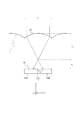
図4は、撮像レンズ並びに撮像素子のマイクロレンズおよび受光部の配置を説明する図である。撮像レンズ11は一つのレンズにより、または、複数のレンズを組み合わせて構成され、絞り32を有する。撮像レンズ11の光軸30は、各マイクロレンズ20の光軸と平行に配置される。受光素子22Lおよび22Rは、受光面34がマイクロレンズ20の後側焦点から所定の距離ずれた後側焦点近傍に配置される。近年のデジタルカメラ向けの撮像レンズの多くは、射出瞳の位置が無限遠付近となるように設計されている。したがって、撮像レンズの射出瞳の像はマイクロレンズ20を通して受光部22L、22Rの受光面34の近傍の瞳共役面36に結像する。
FIG. 4 is a diagram illustrating the arrangement of the imaging lens, the microlens of the imaging device, and the light receiving unit. The
図4では、受光部22L、22Rの受光面34は、撮像レンズ11の瞳と共役に位置する像側の瞳共役面36よりも物体側に位置する。また、図5は、撮像レンズ並びに撮像素子のマイクロレンズおよび受光部の他の配置を説明する図である。受光部22L、22Rの受光面34は、撮像レンズ11の瞳と共役位置に位置する像側の瞳共役面36よりも像側に位置する。
In FIG. 4, the light receiving surfaces 34 of the
図4および図5に示した何れの配置の場合も、被写体光100は、絞り32により絞られ、マイクロレンズアレイ20上に集光され、マイクロレンズ20と受光部22L、22Rとの間に配置されたR、G、Bのカラーフィルタ(図示せず)を介して、受光部22L、22Rによって検出される。受光部22L、22R上には、R、G、Bいずれかの色の光が入射されて被写体像が結像される。
In any of the arrangements shown in FIGS. 4 and 5, the
左側受光部22Lには、主に瞳の左側領域を透過した光(左側光束)が入射し、左側視野の撮像画像を構成する左画素信号を生成する。また、受光部22Rには、主に瞳の右側領域を透過した光(右側光束)が入射し、右側視野の撮像画像を構成する右画素信号を生成する。しかし、撮像レンズ11の瞳と受光部22L,22Rの受光面34とは共役関係から外れているため、左眼用の受光部22Lと右眼用の受光部22Rとに入射する被写体光100の間にクロストークが発生する。
Light (left beam) that has mainly passed through the left region of the pupil is incident on the left
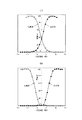
図6は、撮像素子への被写体光の入射角度と左画素信号および右画素信号の信号光強度との関係を示す図であり、図6(a)は、本実施の形態の場合、図6(b)は撮像レンズの瞳面と受光素子の受光面とを共役関係にした場合を示す。本実施の形態では、図6(a)に示すように、左側受光部22Lと右側受光部22Rとの間のクロストークによって、入射角度が0度であっても、受光素子22L、22Rにある程度の強度の光が検出される。これに対して、撮像レンズ11の瞳面と受光部22L、22Rの受光面34とが共役関係にある場合は、図6(b)に示すように、左側受光部22Lと右側受光部22Rとの分離がなされているものの、角度が0度付近で左側受光部22Lおよび右側受光部22Rのいずれも、ほぼ光を検出しない角度範囲が存在する。図6(a)のように撮像レンズ11の瞳と受光部22L、22Rの受光面34とが共役関係から外れた場合、左画素と右画素とで異なる視野の信号が得られ、3次元画像情報の取得に適用でき、各マイクロレンズ20に対応した左画素信号および右画素信号をそれぞれ加算して2次元画像を生成する場合、二重線が現れない自然な画像を生成することができる。
FIG. 6 is a diagram showing the relationship between the incident angle of the subject light to the image sensor and the signal light intensity of the left pixel signal and the right pixel signal. FIG. 6A shows the relationship between the present embodiment and FIG. (B) shows the case where the pupil plane of the imaging lens and the light receiving surface of the light receiving element are in a conjugate relationship. In the present embodiment, as shown in FIG. 6A, due to crosstalk between the left
次に、左側受光部22Lおよび右側受光部22Rを用い、3次元画像生成のための視差画像が得られるとともに、これらの出力信号を加算して自然な2次元画像が生成できるための条件について、図7を参照して説明する。
Next, using the left
まず、マイクロレンズ20の曲率半径をr、マイクロレンズ20から受光部22L、22Rの受光面34までの媒質の平均屈折率をnavとすると、マイクロレンズ20の焦点距離fLは、
![]()
![]()
左側受光部22Lには左側光束の大部分に加え右側光束の一部が入射し、右側受光部22Rには右側光束の大部分に加え左側光束の一部が入射する。それぞれの受光部22L,22Rに入射する反対側の光束の光量は、それぞれの光束の光量の2%から10%までが望ましい。つまり、マイクロレンズ20のピッチをpとすると、受光部22L、22Rの受光面34上でのボケの幅sbは、
0.02p<sb<0.1p (2)
であることが望ましい。
In addition to the majority of the left beam, a part of the right beam is incident on the left
0.02p <sb <0.1p (2)
It is desirable that
また、左右の受光部22L,22Rの間に不感帯がある場合、その幅をSとすると、受光面34上でのボケの幅sbは、
0.02p+S<sb<0.1p+S (3)
が望ましい。
Further, when there is a dead zone between the left and right
0.02p + S <sb <0.1p + S (3)
Is desirable.
式(3)が充足される条件を以下に検討する。 The conditions under which equation (3) is satisfied are discussed below.
まず、図7に示すように受光部22L、22Rの一方のボケの幅をhとする。このとき、
sb=2h (4)
となる。
式(4)に式(3)を代入すると、
0.02p+S<2h<0.1p+S (5)
となる。
First, as shown in FIG. 7, the width of one blur of the
sb = 2h (4)
It becomes.
Substituting equation (3) into equation (4),
0.02p + S <2h <0.1p + S (5)
It becomes.
ここで、前述のように、マイクロレンズ20の焦点受光面34とのずれ量をzdとする。hとずれ量zdの関係は、図7から、
![]()
![]()
![]()
![]()
さらに、式(5)に式(7)を代入して、変形すると、
![]()
![]()
図4に示した後ろ側の焦点ずれと、図5に示した前側の焦点ずれとでは、対称的であるため、絶対値を付して
ここで、受光素子22L、22Rに入射する反対側の光束の光量が、それぞれの光束の光量の2%から10%までが望ましいことの根拠を説明する。
Here, the grounds that the light amount of the opposite side light beams incident on the
図8は、クロストークが発生する場合の光軸における光強度を説明する図である。図8の破線は、ずれ量がほぼ0の場合の被写体光100の入射角度に対する右側受光部22Rおよび左側受光部22Lで受光される光の強度(すなわち、右画素信号および左画素信号)を示している。光強度は、光束の光強度の最大値を100%としてこれに対する比率で示している。ずれ量が0の場合、右側光束および左側光束はともに入射角度0度付近で0に近い値となる。
FIG. 8 is a diagram illustrating the light intensity at the optical axis when crosstalk occurs. The broken lines in FIG. 8 indicate the intensity of light received by the right
一方、図8の実線は、受光面34をマイクロレンズ20の焦点からずらした場合を示している。この場合、左側光束が右側受光素子22Lによって受光されるクロストークの部分を網掛けで示している。本願発明者らによるシミュレーションの結果、クロストークの量が片側の光束の全体の光量の2%であっても、入射角度0度における光強度は、20〜30%程度にもなる。したがって、2次元画像を生成するため、右側受光部22Rと左側受光部22Lとの信号を加算した場合、入射角度0度から入射した光による信号も他の入射角度からの信号と比べ40〜60%の強度の信号が得られる。このため、この程度の強度の信号が得られるのであれば、入射角度0度付近の信号を得ることができないことによる、二重線の発生などを抑制し自然な画像を得ることができる。よって、左右一方の側の光束が他方の受光部22L、22Rに入射する光の量は2%以上であることが好ましい。
On the other hand, the solid line in FIG. 8 shows a case where the
一方、3次元画像の奥行き精度の面では、クロストークは少ない方が好ましい。奥行き精度は、視差量、画素ピッチなどで決定される。そして、瞳分割方式で3次元画像情報(奥行き情報)を取得する場合の視差量は、瞳径/2により定義される。仮にクロストークの量が10%とすると、瞳径は20%減少するので奥行き分解能は20%減少する。 On the other hand, in terms of depth accuracy of the three-dimensional image, it is preferable that the crosstalk is small. The depth accuracy is determined by the amount of parallax, the pixel pitch, and the like. The amount of parallax when acquiring three-dimensional image information (depth information) by the pupil division method is defined by pupil diameter / 2. If the amount of crosstalk is 10%, the pupil diameter is reduced by 20%, and the depth resolution is reduced by 20%.
例えば、焦点距離を35mm、F値を3.5とするとき、瞳径は10mmである。また、クロストークや光量ロスが無い場合、計算上の視差量は5mmである。撮像素子10のピッチを5μmとすると、光学系から物体までの距離(物体距離)が5mの位置で奥行き分解能は620mmとなる。これに対して、同じ条件で片側の受光部22Lまたは22Rへのクロストークが10%ある場合、瞳径が20%減少するので、視差量は4mmとなり、奥行き分解能は745mmとなる。分解能が2割以上減少することは好ましくないので、左右一方の側の光束が他方の受光素子22L、22Rに入射する光の量は10%以下であることが好ましい。
For example, when the focal length is 35 mm and the F value is 3.5, the pupil diameter is 10 mm. Further, when there is no crosstalk or light amount loss, the calculated parallax amount is 5 mm. When the pitch of the
(実施例)
マイクロレンズ20のピッチを10μm、焦点距離を12.5μm、不感帯の幅を0.2μm、ずれ量を1μmとする場合、
When the
以上説明したように、本実施の形態によれば、撮像レンズ11の瞳と受光部22L、22Rの受光面34とを共役関係から外れるように配置したので、3次元画像を生成するための視差画像が得られるとともに、2次元画像を作成する場合には左眼用および右眼用の受光素子22L、22Rからの検出信号を加算してより自然な画像が得られる。
As described above, according to the present embodiment, since the pupil of the
さらに、式(9)に示す条件を満たすことにより、奥行き分解能を確保した3次元画像が生成できると共に、2次元画像を表示する際には入射角度0度近傍の信号を含む二重線の現れないより自然な画像が得られる。 Furthermore, by satisfying the condition shown in Expression (9), a three-dimensional image with depth resolution can be generated, and a double line including a signal near an incident angle of 0 degrees appears when displaying a two-dimensional image. A more natural image is obtained.
(第2実施の形態)
図9は、第2実施の形態に係る撮像素子の構成を説明する平面図であり、図10は、第2実施の形態に係る撮像素子の構成を説明する斜視図である。本実施の形態では、第1実施の形態と同様に、左側および右側受光部22L、22Rが交互に並んで配列されている。各受光部22L,22Rの間には配線層23が設けられている。さらに、受光部の上方(Z軸方向)にはY軸方向に軸を有するシリンドリカルレンズ41がX軸方向に並べられて配置され、各左側および右側受光部22L、22Rの組は同一のシリンドリカルレンズ41の下方に配置されている。また、一つのシリンドリカルレンズ41の下方には、左側および右側受光部22L、22Rの組から成る複数の受光部対22が配置されている。シリンドリカルレンズ41は、X軸方向にのみ集光作用を有し、受光素子22L、22Rの受光面34と撮像レンズ11の瞳とは共役関係から外れて配置される。その他の構成は、第1実施の形態と同様であるので、同一または対応する構成要素には同一参照符号を付して説明を省略する。
(Second Embodiment)
FIG. 9 is a plan view illustrating the configuration of the image sensor according to the second embodiment, and FIG. 10 is a perspective view illustrating the configuration of the image sensor according to the second embodiment. In the present embodiment, as in the first embodiment, the left and right
本実施の形態によれば、第1実施の形態と同様に、被写体光100の、撮像レンズ11の瞳の左側を通る左側光束と右側を通る右側光束とを、シリンドリカルレンズ41を透過させ、それぞれ異なる左側受光部22Lおよび右側受光部22Rに入射させて検出することができる。さらに、受光部22L、22Rの受光面34は、撮像レンズ11の瞳と共役な位置からずらして配置されているので、左側光束と右側光束とがそれぞれ部分的に右側受光素子22Rおよび左側受光部22Lに入射する。これによって、3次元画像を生成するための視差情報を含む左画素および右画素の画素信号が得られるとともに、左画素と右画素の画素信号を加算することにより、二重線の現れない自然な2次元画像を生成することができる。
According to the present embodiment, similarly to the first embodiment, the left luminous flux passing through the left side of the pupil of the
(第3実施の形態)
図11は、第3実施の形態に係る撮像素子の構成を説明する図である。本実施の形態では、1つのマイクロレンズ20に対して、各2つの受光素子が配置されている。受光部としては、被写体像の結像される水平方向に左側受光部51Lおよび右側受光部51Rが配置されるものと、垂直方向に上側受光部51Uおよび下側受光部51Dが配置されるものの2種類がある。これら受光素子51L、51R、51U、51Dの受光面34は、撮像レンズ11の瞳と共役関係から外れた位置に配置される。その他の構成は、第1実施の形態と同様であるので、同一または対応する構成要素には同一参照符号を付して説明を省略する。
(Third embodiment)
FIG. 11 is a diagram illustrating a configuration of an image sensor according to the third embodiment. In the present embodiment, two light receiving elements are arranged for one
本実施の形態によれば、水平方向に配置された受光部51L、51Rを用いて、第1実施の形態と同様に3次元画像を生成するための視差画像を撮像することができるとともに、2次元画像を作成する場合には左右の受光部51L、51Rからの画素信号を加算してより自然な画像が得られる。さらに、垂直方向に配置された受光部51Uおよび51Dからの信号に基づいて、垂直方向の視差情報から奥行き情報を得ることもできる。また、垂直方向に配置された受光部51Uおよび51Dの信号を加算して、水平方向に配置された受光部51Lおよび51Rを加算した信号とともに、2次元画像の作成に用いることができる。
According to the present embodiment, it is possible to pick up a parallax image for generating a three-dimensional image using the light receiving units 51L and 51R arranged in the horizontal direction, as in the first embodiment, and 2 When creating a dimensional image, pixel signals from the left and right light receiving portions 51L and 51R are added to obtain a more natural image. Furthermore, depth information can be obtained from the parallax information in the vertical direction based on signals from the
(第4実施の形態)
図12は、第3実施の形態に係る撮像素子10の構成を説明する図である。本実施の形態では、1つのマイクロレンズ20に対して、水平方向および垂直方向に各2列の合計4つの受光部61DL、61DR、61UL,61URが配置されている。ここで、各受光部61DL、61DR、61UL,61URは、撮像レンズ11の瞳を水平な直線および鉛直な直線で4分割した場合の順に左下側、右下側、左上側、右上側の分割された瞳に対応するものである。これら受光部61DL、61DR、61UL、61URの受光面34は、撮像レンズ11の瞳と共役関係から外れた位置に配置される。その他の構成は、第1実施の形態と同様であるので、同一または対応する構成要素には同一参照符号を付して説明を省略する。
(Fourth embodiment)
FIG. 12 is a diagram illustrating the configuration of the
本実施の形態によれば、撮像素子10の左右の画素対、すなわち受光部61DLと61DRおよび/または61ULと61URから出力される画素信号に基づいて、第1実施の形態と同様に立体画像を生成でき、1つのマイクロレンズ20に対応する受光部61DL、61DR、61ULおよび61URの信号を加算することによって2次元画像の画素信号とし、2次元画像を生成することができる。これによって、第1実施の形態と同様の効果が得られる。さらに、撮像素子10の上下の画素対、すなわち受光部61DLと61ULおよび/または61URと61URから出力される画素信号に基づいて、垂直方向の視差情報も得ることができる。したがって、同じ撮像素子を用いながら、上下および左右の視差情報を得ることができる。
According to the present embodiment, a stereoscopic image is generated based on pixel signals output from the left and right pixel pairs of the
なお、本発明は、上記実施の形態にのみ限定されるものではなく、幾多の変形または変更が可能である。たとえば、1つのマイクロレンズに対する受光部の数は、2個または4個に限られない。また、受光素子の配列の方向も左右および上下に限られない。例えば、斜め方向に配列された受光素子対を有していても良い。また、表示部は必ずしも撮像装置と一体である必要は無く、3次元画像を表示するために別体のハードウェアとして設けられていても良い。 In addition, this invention is not limited only to the said embodiment, Many deformation | transformation or a change is possible. For example, the number of light receiving units for one microlens is not limited to two or four. Further, the direction of the arrangement of the light receiving elements is not limited to the left and right and the top and bottom. For example, you may have the light receiving element pair arranged in the diagonal direction. Further, the display unit does not necessarily have to be integrated with the imaging device, and may be provided as separate hardware for displaying a three-dimensional image.
1 撮像装置
2 マイクロレンズアレイ
10 撮像部
11 撮像レンズ
12 画像処理部
14 制御部
16 記憶部
18 表示部
19 バス
20 マイクロレンズ
22 受光素子対
22L、22R 受光部
23 配線層
30 光軸
32 絞り
34 受光面
36 瞳共役面
41 シリンドリカルレンズ
51L,51R,51U,51D 受光部
61DL,61DR,61UL,61UR 受光部
100 被写体光
DESCRIPTION OF SYMBOLS 1 Imaging device 2
Claims (8)
被写体からの光を前記マイクロレンズアレイに結像させる撮像レンズと、
前記マイクロレンズごとにそれぞれ複数ずつ配置された受光部であって、各マイクロレンズに対応する複数の前記受光部の少なくとも2つは、前記マイクロレンズに結像された前記被写体からの光を受光し光電変換する前記受光部と
を備え、
前記撮像レンズの瞳と前記受光部の受光面とは、共役関係から外れるように配置されることを特徴とする撮像装置。 A microlens array having a plurality of microlenses regularly arranged two-dimensionally;
An imaging lens for imaging light from a subject on the microlens array;
A plurality of light receiving units arranged for each of the micro lenses, wherein at least two of the plurality of light receiving units corresponding to the micro lenses receive light from the subject imaged on the micro lens. Including the light receiving unit that performs photoelectric conversion,
Wherein the pupil and the light receiving surface of the light receiving portion of the imaging lens, you being arranged so as deviate from a conjugated relationship imaging device.
が成り立つことを特徴とする請求項1に記載の撮像装置。 The focal length of the microlens is f L , the pitch of the microlens is p, the width of the dead zone located between the light receiving sections corresponding to the same microlens, the light receiving surface of the light receiving section and the imaging when the amount of deviation between the conjugate position of the pupil of the lens and Z d,
The imaging apparatus according to claim 1, wherein:
Generating at least one of a plurality of parallax images having parallax with each other based on pixel signals obtained from the plurality of light receiving units and a two-dimensional image obtained by adding corresponding pixel signals obtained from the plurality of light receiving units. Item 2. The imaging device according to Item 1.
Priority Applications (5)
| Application Number | Priority Date | Filing Date | Title |
|---|---|---|---|
| JP2012246651A JP5584270B2 (en) | 2012-11-08 | 2012-11-08 | Imaging device |
| PCT/JP2013/006242 WO2014073172A1 (en) | 2012-11-08 | 2013-10-22 | Image capture device |
| US14/534,742 US9190436B2 (en) | 2012-11-08 | 2014-11-06 | Imaging apparatus |
| US14/918,973 US9305957B2 (en) | 2012-11-08 | 2015-10-21 | Imaging apparatus |
| US15/058,856 US9419037B2 (en) | 2012-11-08 | 2016-03-02 | Imaging apparatus |
Applications Claiming Priority (1)
| Application Number | Priority Date | Filing Date | Title |
|---|---|---|---|
| JP2012246651A JP5584270B2 (en) | 2012-11-08 | 2012-11-08 | Imaging device |
Related Child Applications (1)
| Application Number | Title | Priority Date | Filing Date |
|---|---|---|---|
| JP2014146826A Division JP5810196B2 (en) | 2014-07-17 | 2014-07-17 | Imaging device |
Publications (3)
| Publication Number | Publication Date |
|---|---|
| JP2014096683A JP2014096683A (en) | 2014-05-22 |
| JP2014096683A5 JP2014096683A5 (en) | 2014-07-10 |
| JP5584270B2 true JP5584270B2 (en) | 2014-09-03 |
Family
ID=50684298
Family Applications (1)
| Application Number | Title | Priority Date | Filing Date |
|---|---|---|---|
| JP2012246651A Expired - Fee Related JP5584270B2 (en) | 2012-11-08 | 2012-11-08 | Imaging device |
Country Status (3)
| Country | Link |
|---|---|
| US (3) | US9190436B2 (en) |
| JP (1) | JP5584270B2 (en) |
| WO (1) | WO2014073172A1 (en) |
Families Citing this family (6)
| Publication number | Priority date | Publication date | Assignee | Title |
|---|---|---|---|---|
| US9978154B2 (en) * | 2015-07-02 | 2018-05-22 | Pixart Imaging Inc. | Distance measurement device base on phase difference and distance measurement method thereof |
| US10148864B2 (en) | 2015-07-02 | 2018-12-04 | Pixart Imaging Inc. | Imaging device having phase detection pixels and regular pixels, and operating method thereof |
| US10790325B2 (en) | 2015-07-29 | 2020-09-29 | Samsung Electronics Co., Ltd. | Imaging apparatus and image sensor including the same |
| US11089286B2 (en) | 2015-07-29 | 2021-08-10 | Samsung Electronics Co., Ltd. | Image sensor |
| US11469265B2 (en) | 2015-07-29 | 2022-10-11 | Samsung Electronics Co., Ltd. | Imaging apparatus and image sensor including the same |
| US10403668B2 (en) * | 2015-07-29 | 2019-09-03 | Samsung Electronics Co., Ltd. | Imaging apparatus and image sensor including the same |
Family Cites Families (11)
| Publication number | Priority date | Publication date | Assignee | Title |
|---|---|---|---|---|
| US6396873B1 (en) | 1999-02-25 | 2002-05-28 | Envision Advanced Medical Systems | Optical device |
| WO2007011026A1 (en) * | 2005-07-22 | 2007-01-25 | Nikon Corporation | Imaging element, focal point detecting device, and imaging system |
| JP4839990B2 (en) * | 2006-07-06 | 2011-12-21 | 株式会社ニコン | Solid-state imaging device and imaging apparatus using the same |
| US20090219432A1 (en) | 2008-02-29 | 2009-09-03 | Palum Russell J | Sensor with multi-perspective image capture |
| EP2146248B1 (en) * | 2008-07-16 | 2012-08-29 | Carl Zeiss SMT GmbH | Illumination system of a microlithographic projection exposure apparatus |
| JP5245716B2 (en) * | 2008-10-27 | 2013-07-24 | 株式会社ニコン | Camera lens adapter and camera system |
| US8749620B1 (en) * | 2010-02-20 | 2014-06-10 | Lytro, Inc. | 3D light field cameras, images and files, and methods of using, operating, processing and viewing same |
| JP5513326B2 (en) * | 2010-09-07 | 2014-06-04 | キヤノン株式会社 | Imaging device and imaging apparatus |
| JP5864990B2 (en) * | 2011-10-03 | 2016-02-17 | キヤノン株式会社 | Solid-state imaging device and camera |
| JP5743837B2 (en) * | 2011-10-07 | 2015-07-01 | キヤノン株式会社 | Photoelectric conversion device, imaging device, and imaging system |
| JP5818697B2 (en) * | 2012-01-13 | 2015-11-18 | キヤノン株式会社 | Image generation method, imaging device, display device, program, and storage medium |
-
2012
- 2012-11-08 JP JP2012246651A patent/JP5584270B2/en not_active Expired - Fee Related
-
2013
- 2013-10-22 WO PCT/JP2013/006242 patent/WO2014073172A1/en active Application Filing
-
2014
- 2014-11-06 US US14/534,742 patent/US9190436B2/en not_active Expired - Fee Related
-
2015
- 2015-10-21 US US14/918,973 patent/US9305957B2/en active Active
-
2016
- 2016-03-02 US US15/058,856 patent/US9419037B2/en active Active
Also Published As
| Publication number | Publication date |
|---|---|
| US9419037B2 (en) | 2016-08-16 |
| US20160181300A1 (en) | 2016-06-23 |
| US9190436B2 (en) | 2015-11-17 |
| US20160043124A1 (en) | 2016-02-11 |
| JP2014096683A (en) | 2014-05-22 |
| WO2014073172A1 (en) | 2014-05-15 |
| US9305957B2 (en) | 2016-04-05 |
| US20150061066A1 (en) | 2015-03-05 |
Similar Documents
| Publication | Publication Date | Title |
|---|---|---|
| JP5982751B2 (en) | Image processing apparatus, image processing method, and program | |
| JP5584270B2 (en) | Imaging device | |
| JP5538553B2 (en) | Solid-state imaging device and imaging apparatus | |
| US9851483B2 (en) | Stereoscopic imaging method and system that divides a pixel matrix into subgroups | |
| US9036004B2 (en) | Three-dimensional image capture device | |
| EP2579568B1 (en) | Imaging device and imaging method | |
| US20120112037A1 (en) | Three-dimensional imaging device | |
| US20120105598A1 (en) | Three-dimensional imaging device | |
| WO2013136819A1 (en) | Image sensor, imaging device and imaging system | |
| JP6288088B2 (en) | Imaging device | |
| JP5810196B2 (en) | Imaging device | |
| JP6197316B2 (en) | Imaging device and imaging apparatus | |
| WO2014064867A1 (en) | Imaging element and imaging device | |
| JP2009021708A (en) | Element image group conversion device, stereoscopic image display device, and element image group conversion program | |
| JP5979137B2 (en) | IMAGING DEVICE AND IMAGING DEVICE CONTROL PROGRAM | |
| JP6234024B2 (en) | Imaging device and imaging apparatus | |
| JP6086681B2 (en) | Imaging device and imaging apparatus | |
| JP2013239787A (en) | Imaging element and imaging apparatus using the same | |
| JP6205770B2 (en) | Imaging device and imaging system | |
| JP5452800B2 (en) | Stereoscopic imaging device | |
| JP5853510B2 (en) | Imaging device | |
| JP2014215405A (en) | Imaging element and microscope device |
Legal Events
| Date | Code | Title | Description |
|---|---|---|---|
| A521 | Request for written amendment filed |
Free format text: JAPANESE INTERMEDIATE CODE: A523 Effective date: 20140527 |
|
| A621 | Written request for application examination |
Free format text: JAPANESE INTERMEDIATE CODE: A621 Effective date: 20140527 |
|
| A871 | Explanation of circumstances concerning accelerated examination |
Free format text: JAPANESE INTERMEDIATE CODE: A871 Effective date: 20140527 |
|
| TRDD | Decision of grant or rejection written | ||
| A975 | Report on accelerated examination |
Free format text: JAPANESE INTERMEDIATE CODE: A971005 Effective date: 20140612 |
|
| A01 | Written decision to grant a patent or to grant a registration (utility model) |
Free format text: JAPANESE INTERMEDIATE CODE: A01 Effective date: 20140617 |
|
| A61 | First payment of annual fees (during grant procedure) |
Free format text: JAPANESE INTERMEDIATE CODE: A61 Effective date: 20140717 |
|
| R150 | Certificate of patent or registration of utility model |
Ref document number: 5584270 Country of ref document: JP Free format text: JAPANESE INTERMEDIATE CODE: R150 |
|
| S531 | Written request for registration of change of domicile |
Free format text: JAPANESE INTERMEDIATE CODE: R313531 |
|
| R350 | Written notification of registration of transfer |
Free format text: JAPANESE INTERMEDIATE CODE: R350 |
|
| R250 | Receipt of annual fees |
Free format text: JAPANESE INTERMEDIATE CODE: R250 |
|
| R250 | Receipt of annual fees |
Free format text: JAPANESE INTERMEDIATE CODE: R250 |
|
| LAPS | Cancellation because of no payment of annual fees |