JP5580602B2 - Cascode circuit using depletion mode GaN-based FET - Google Patents
Cascode circuit using depletion mode GaN-based FET Download PDFInfo
- Publication number
- JP5580602B2 JP5580602B2 JP2009554725A JP2009554725A JP5580602B2 JP 5580602 B2 JP5580602 B2 JP 5580602B2 JP 2009554725 A JP2009554725 A JP 2009554725A JP 2009554725 A JP2009554725 A JP 2009554725A JP 5580602 B2 JP5580602 B2 JP 5580602B2
- Authority
- JP
- Japan
- Prior art keywords
- active layer
- layer
- mode fet
- circuit
- source
- Prior art date
- Legal status (The legal status is an assumption and is not a legal conclusion. Google has not performed a legal analysis and makes no representation as to the accuracy of the status listed.)
- Expired - Fee Related
Links
- 239000000758 substrate Substances 0.000 claims description 27
- 239000000463 material Substances 0.000 claims description 17
- 239000004065 semiconductor Substances 0.000 claims description 15
- 229910052751 metal Inorganic materials 0.000 claims description 11
- 239000002184 metal Substances 0.000 claims description 11
- 229910002704 AlGaN Inorganic materials 0.000 claims description 10
- 230000006911 nucleation Effects 0.000 claims description 10
- 238000010899 nucleation Methods 0.000 claims description 10
- 229910001218 Gallium arsenide Inorganic materials 0.000 claims description 4
- 230000005533 two-dimensional electron gas Effects 0.000 claims description 4
- 229910052710 silicon Inorganic materials 0.000 claims description 3
- 239000010703 silicon Substances 0.000 claims description 3
- 229910017464 nitrogen compound Inorganic materials 0.000 claims 9
- 150000002830 nitrogen compounds Chemical class 0.000 claims 9
- 239000010410 layer Substances 0.000 description 120
- JMASRVWKEDWRBT-UHFFFAOYSA-N Gallium nitride Chemical compound [Ga]#N JMASRVWKEDWRBT-UHFFFAOYSA-N 0.000 description 45
- 229910002601 GaN Inorganic materials 0.000 description 43
- 230000004888 barrier function Effects 0.000 description 8
- 238000000034 method Methods 0.000 description 7
- 229910052782 aluminium Inorganic materials 0.000 description 6
- XAGFODPZIPBFFR-UHFFFAOYSA-N aluminium Chemical compound [Al] XAGFODPZIPBFFR-UHFFFAOYSA-N 0.000 description 5
- 229910052733 gallium Inorganic materials 0.000 description 5
- 239000007789 gas Substances 0.000 description 5
- QGZKDVFQNNGYKY-UHFFFAOYSA-N Ammonia Chemical compound N QGZKDVFQNNGYKY-UHFFFAOYSA-N 0.000 description 4
- GYHNNYVSQQEPJS-UHFFFAOYSA-N Gallium Chemical compound [Ga] GYHNNYVSQQEPJS-UHFFFAOYSA-N 0.000 description 4
- 230000015556 catabolic process Effects 0.000 description 4
- 229910052738 indium Inorganic materials 0.000 description 4
- -1 nitride compound Chemical class 0.000 description 4
- 230000008569 process Effects 0.000 description 4
- 239000013078 crystal Substances 0.000 description 3
- APFVFJFRJDLVQX-UHFFFAOYSA-N indium atom Chemical compound [In] APFVFJFRJDLVQX-UHFFFAOYSA-N 0.000 description 3
- 230000003647 oxidation Effects 0.000 description 3
- 238000007254 oxidation reaction Methods 0.000 description 3
- 238000002161 passivation Methods 0.000 description 3
- 238000007740 vapor deposition Methods 0.000 description 3
- IJGRMHOSHXDMSA-UHFFFAOYSA-N Atomic nitrogen Chemical compound N#N IJGRMHOSHXDMSA-UHFFFAOYSA-N 0.000 description 2
- PXHVJJICTQNCMI-UHFFFAOYSA-N Nickel Chemical compound [Ni] PXHVJJICTQNCMI-UHFFFAOYSA-N 0.000 description 2
- 229910021529 ammonia Inorganic materials 0.000 description 2
- 230000015572 biosynthetic process Effects 0.000 description 2
- 230000000903 blocking effect Effects 0.000 description 2
- 150000001875 compounds Chemical class 0.000 description 2
- 238000000151 deposition Methods 0.000 description 2
- 239000002019 doping agent Substances 0.000 description 2
- PCHJSUWPFVWCPO-UHFFFAOYSA-N gold Chemical compound [Au] PCHJSUWPFVWCPO-UHFFFAOYSA-N 0.000 description 2
- 229910052737 gold Inorganic materials 0.000 description 2
- 239000010931 gold Substances 0.000 description 2
- 238000004519 manufacturing process Methods 0.000 description 2
- 239000007769 metal material Substances 0.000 description 2
- 150000004767 nitrides Chemical class 0.000 description 2
- QJGQUHMNIGDVPM-UHFFFAOYSA-N nitrogen group Chemical group [N] QJGQUHMNIGDVPM-UHFFFAOYSA-N 0.000 description 2
- 125000002524 organometallic group Chemical group 0.000 description 2
- 238000005240 physical vapour deposition Methods 0.000 description 2
- 229910052594 sapphire Inorganic materials 0.000 description 2
- 239000010980 sapphire Substances 0.000 description 2
- ZOXJGFHDIHLPTG-UHFFFAOYSA-N Boron Chemical compound [B] ZOXJGFHDIHLPTG-UHFFFAOYSA-N 0.000 description 1
- 208000032750 Device leakage Diseases 0.000 description 1
- RTAQQCXQSZGOHL-UHFFFAOYSA-N Titanium Chemical compound [Ti] RTAQQCXQSZGOHL-UHFFFAOYSA-N 0.000 description 1
- 238000009825 accumulation Methods 0.000 description 1
- 239000000956 alloy Substances 0.000 description 1
- 229910045601 alloy Inorganic materials 0.000 description 1
- 238000003877 atomic layer epitaxy Methods 0.000 description 1
- 229910052796 boron Inorganic materials 0.000 description 1
- 239000000969 carrier Substances 0.000 description 1
- 238000005229 chemical vapour deposition Methods 0.000 description 1
- 238000007796 conventional method Methods 0.000 description 1
- PMHQVHHXPFUNSP-UHFFFAOYSA-M copper(1+);methylsulfanylmethane;bromide Chemical compound Br[Cu].CSC PMHQVHHXPFUNSP-UHFFFAOYSA-M 0.000 description 1
- 239000002178 crystalline material Substances 0.000 description 1
- 230000007547 defect Effects 0.000 description 1
- 238000005530 etching Methods 0.000 description 1
- 230000005669 field effect Effects 0.000 description 1
- 150000004678 hydrides Chemical class 0.000 description 1
- 238000011065 in-situ storage Methods 0.000 description 1
- 150000002739 metals Chemical class 0.000 description 1
- 230000005012 migration Effects 0.000 description 1
- 238000013508 migration Methods 0.000 description 1
- 239000000203 mixture Substances 0.000 description 1
- 238000012986 modification Methods 0.000 description 1
- 230000004048 modification Effects 0.000 description 1
- 238000001451 molecular beam epitaxy Methods 0.000 description 1
- 229910052759 nickel Inorganic materials 0.000 description 1
- 229910052757 nitrogen Inorganic materials 0.000 description 1
- 150000002902 organometallic compounds Chemical class 0.000 description 1
- NRNCYVBFPDDJNE-UHFFFAOYSA-N pemoline Chemical compound O1C(N)=NC(=O)C1C1=CC=CC=C1 NRNCYVBFPDDJNE-UHFFFAOYSA-N 0.000 description 1
- 230000035515 penetration Effects 0.000 description 1
- 238000005036 potential barrier Methods 0.000 description 1
- 238000005381 potential energy Methods 0.000 description 1
- 238000005546 reactive sputtering Methods 0.000 description 1
- 230000009467 reduction Effects 0.000 description 1
- HBMJWWWQQXIZIP-UHFFFAOYSA-N silicon carbide Chemical compound [Si+]#[C-] HBMJWWWQQXIZIP-UHFFFAOYSA-N 0.000 description 1
- 239000002356 single layer Substances 0.000 description 1
- 238000006557 surface reaction Methods 0.000 description 1
- 230000003746 surface roughness Effects 0.000 description 1
- 229910052719 titanium Inorganic materials 0.000 description 1
- 239000010936 titanium Substances 0.000 description 1
- 230000007704 transition Effects 0.000 description 1
Images


Classifications
-
- H—ELECTRICITY
- H03—ELECTRONIC CIRCUITRY
- H03K—PULSE TECHNIQUE
- H03K19/00—Logic circuits, i.e. having at least two inputs acting on one output; Inverting circuits
- H03K19/02—Logic circuits, i.e. having at least two inputs acting on one output; Inverting circuits using specified components
- H03K19/08—Logic circuits, i.e. having at least two inputs acting on one output; Inverting circuits using specified components using semiconductor devices
- H03K19/094—Logic circuits, i.e. having at least two inputs acting on one output; Inverting circuits using specified components using semiconductor devices using field-effect transistors
- H03K19/0952—Logic circuits, i.e. having at least two inputs acting on one output; Inverting circuits using specified components using semiconductor devices using field-effect transistors using Schottky type FET MESFET
-
- H—ELECTRICITY
- H01—ELECTRIC ELEMENTS
- H01L—SEMICONDUCTOR DEVICES NOT COVERED BY CLASS H10
- H01L27/00—Devices consisting of a plurality of semiconductor or other solid-state components formed in or on a common substrate
- H01L27/02—Devices consisting of a plurality of semiconductor or other solid-state components formed in or on a common substrate including semiconductor components specially adapted for rectifying, oscillating, amplifying or switching and having at least one potential-jump barrier or surface barrier; including integrated passive circuit elements with at least one potential-jump barrier or surface barrier
- H01L27/04—Devices consisting of a plurality of semiconductor or other solid-state components formed in or on a common substrate including semiconductor components specially adapted for rectifying, oscillating, amplifying or switching and having at least one potential-jump barrier or surface barrier; including integrated passive circuit elements with at least one potential-jump barrier or surface barrier the substrate being a semiconductor body
- H01L27/06—Devices consisting of a plurality of semiconductor or other solid-state components formed in or on a common substrate including semiconductor components specially adapted for rectifying, oscillating, amplifying or switching and having at least one potential-jump barrier or surface barrier; including integrated passive circuit elements with at least one potential-jump barrier or surface barrier the substrate being a semiconductor body including a plurality of individual components in a non-repetitive configuration
- H01L27/0605—Devices consisting of a plurality of semiconductor or other solid-state components formed in or on a common substrate including semiconductor components specially adapted for rectifying, oscillating, amplifying or switching and having at least one potential-jump barrier or surface barrier; including integrated passive circuit elements with at least one potential-jump barrier or surface barrier the substrate being a semiconductor body including a plurality of individual components in a non-repetitive configuration integrated circuits made of compound material, e.g. AIIIBV
-
- H—ELECTRICITY
- H01—ELECTRIC ELEMENTS
- H01L—SEMICONDUCTOR DEVICES NOT COVERED BY CLASS H10
- H01L29/00—Semiconductor devices adapted for rectifying, amplifying, oscillating or switching, or capacitors or resistors with at least one potential-jump barrier or surface barrier, e.g. PN junction depletion layer or carrier concentration layer; Details of semiconductor bodies or of electrodes thereof ; Multistep manufacturing processes therefor
- H01L29/02—Semiconductor bodies ; Multistep manufacturing processes therefor
- H01L29/12—Semiconductor bodies ; Multistep manufacturing processes therefor characterised by the materials of which they are formed
- H01L29/20—Semiconductor bodies ; Multistep manufacturing processes therefor characterised by the materials of which they are formed including, apart from doping materials or other impurities, only AIIIBV compounds
- H01L29/2003—Nitride compounds
-
- H—ELECTRICITY
- H01—ELECTRIC ELEMENTS
- H01L—SEMICONDUCTOR DEVICES NOT COVERED BY CLASS H10
- H01L29/00—Semiconductor devices adapted for rectifying, amplifying, oscillating or switching, or capacitors or resistors with at least one potential-jump barrier or surface barrier, e.g. PN junction depletion layer or carrier concentration layer; Details of semiconductor bodies or of electrodes thereof ; Multistep manufacturing processes therefor
- H01L29/66—Types of semiconductor device ; Multistep manufacturing processes therefor
- H01L29/66007—Multistep manufacturing processes
- H01L29/66075—Multistep manufacturing processes of devices having semiconductor bodies comprising group 14 or group 13/15 materials
- H01L29/66227—Multistep manufacturing processes of devices having semiconductor bodies comprising group 14 or group 13/15 materials the devices being controllable only by the electric current supplied or the electric potential applied, to an electrode which does not carry the current to be rectified, amplified or switched, e.g. three-terminal devices
- H01L29/66409—Unipolar field-effect transistors
- H01L29/66446—Unipolar field-effect transistors with an active layer made of a group 13/15 material, e.g. group 13/15 velocity modulation transistor [VMT], group 13/15 negative resistance FET [NERFET]
- H01L29/66462—Unipolar field-effect transistors with an active layer made of a group 13/15 material, e.g. group 13/15 velocity modulation transistor [VMT], group 13/15 negative resistance FET [NERFET] with a heterojunction interface channel or gate, e.g. HFET, HIGFET, SISFET, HJFET, HEMT
-
- H—ELECTRICITY
- H01—ELECTRIC ELEMENTS
- H01L—SEMICONDUCTOR DEVICES NOT COVERED BY CLASS H10
- H01L29/00—Semiconductor devices adapted for rectifying, amplifying, oscillating or switching, or capacitors or resistors with at least one potential-jump barrier or surface barrier, e.g. PN junction depletion layer or carrier concentration layer; Details of semiconductor bodies or of electrodes thereof ; Multistep manufacturing processes therefor
- H01L29/66—Types of semiconductor device ; Multistep manufacturing processes therefor
- H01L29/68—Types of semiconductor device ; Multistep manufacturing processes therefor controllable by only the electric current supplied, or only the electric potential applied, to an electrode which does not carry the current to be rectified, amplified or switched
- H01L29/76—Unipolar devices, e.g. field effect transistors
- H01L29/772—Field effect transistors
- H01L29/778—Field effect transistors with two-dimensional charge carrier gas channel, e.g. HEMT ; with two-dimensional charge-carrier layer formed at a heterojunction interface
- H01L29/7786—Field effect transistors with two-dimensional charge carrier gas channel, e.g. HEMT ; with two-dimensional charge-carrier layer formed at a heterojunction interface with direct single heterostructure, i.e. with wide bandgap layer formed on top of active layer, e.g. direct single heterostructure MIS-like HEMT
-
- H—ELECTRICITY
- H03—ELECTRONIC CIRCUITRY
- H03F—AMPLIFIERS
- H03F1/00—Details of amplifiers with only discharge tubes, only semiconductor devices or only unspecified devices as amplifying elements
- H03F1/08—Modifications of amplifiers to reduce detrimental influences of internal impedances of amplifying elements
- H03F1/22—Modifications of amplifiers to reduce detrimental influences of internal impedances of amplifying elements by use of cascode coupling, i.e. earthed cathode or emitter stage followed by earthed grid or base stage respectively
- H03F1/226—Modifications of amplifiers to reduce detrimental influences of internal impedances of amplifying elements by use of cascode coupling, i.e. earthed cathode or emitter stage followed by earthed grid or base stage respectively with junction-FET's
-
- H—ELECTRICITY
- H03—ELECTRONIC CIRCUITRY
- H03K—PULSE TECHNIQUE
- H03K17/00—Electronic switching or gating, i.e. not by contact-making and –breaking
- H03K17/51—Electronic switching or gating, i.e. not by contact-making and –breaking characterised by the components used
- H03K17/56—Electronic switching or gating, i.e. not by contact-making and –breaking characterised by the components used by the use, as active elements, of semiconductor devices
- H03K17/567—Circuits characterised by the use of more than one type of semiconductor device, e.g. BIMOS, composite devices such as IGBT
-
- H—ELECTRICITY
- H03—ELECTRONIC CIRCUITRY
- H03K—PULSE TECHNIQUE
- H03K19/00—Logic circuits, i.e. having at least two inputs acting on one output; Inverting circuits
- H03K19/02—Logic circuits, i.e. having at least two inputs acting on one output; Inverting circuits using specified components
- H03K19/08—Logic circuits, i.e. having at least two inputs acting on one output; Inverting circuits using specified components using semiconductor devices
- H03K19/094—Logic circuits, i.e. having at least two inputs acting on one output; Inverting circuits using specified components using semiconductor devices using field-effect transistors
- H03K19/0944—Logic circuits, i.e. having at least two inputs acting on one output; Inverting circuits using specified components using semiconductor devices using field-effect transistors using MOSFET or insulated gate field-effect transistors, i.e. IGFET
- H03K19/0948—Logic circuits, i.e. having at least two inputs acting on one output; Inverting circuits using specified components using semiconductor devices using field-effect transistors using MOSFET or insulated gate field-effect transistors, i.e. IGFET using CMOS or complementary insulated gate field-effect transistors
- H03K19/09482—Logic circuits, i.e. having at least two inputs acting on one output; Inverting circuits using specified components using semiconductor devices using field-effect transistors using MOSFET or insulated gate field-effect transistors, i.e. IGFET using CMOS or complementary insulated gate field-effect transistors using a combination of enhancement and depletion transistors
-
- H—ELECTRICITY
- H01—ELECTRIC ELEMENTS
- H01L—SEMICONDUCTOR DEVICES NOT COVERED BY CLASS H10
- H01L27/00—Devices consisting of a plurality of semiconductor or other solid-state components formed in or on a common substrate
- H01L27/02—Devices consisting of a plurality of semiconductor or other solid-state components formed in or on a common substrate including semiconductor components specially adapted for rectifying, oscillating, amplifying or switching and having at least one potential-jump barrier or surface barrier; including integrated passive circuit elements with at least one potential-jump barrier or surface barrier
- H01L27/04—Devices consisting of a plurality of semiconductor or other solid-state components formed in or on a common substrate including semiconductor components specially adapted for rectifying, oscillating, amplifying or switching and having at least one potential-jump barrier or surface barrier; including integrated passive circuit elements with at least one potential-jump barrier or surface barrier the substrate being a semiconductor body
- H01L27/08—Devices consisting of a plurality of semiconductor or other solid-state components formed in or on a common substrate including semiconductor components specially adapted for rectifying, oscillating, amplifying or switching and having at least one potential-jump barrier or surface barrier; including integrated passive circuit elements with at least one potential-jump barrier or surface barrier the substrate being a semiconductor body including only semiconductor components of a single kind
- H01L27/085—Devices consisting of a plurality of semiconductor or other solid-state components formed in or on a common substrate including semiconductor components specially adapted for rectifying, oscillating, amplifying or switching and having at least one potential-jump barrier or surface barrier; including integrated passive circuit elements with at least one potential-jump barrier or surface barrier the substrate being a semiconductor body including only semiconductor components of a single kind including field-effect components only
- H01L27/088—Devices consisting of a plurality of semiconductor or other solid-state components formed in or on a common substrate including semiconductor components specially adapted for rectifying, oscillating, amplifying or switching and having at least one potential-jump barrier or surface barrier; including integrated passive circuit elements with at least one potential-jump barrier or surface barrier the substrate being a semiconductor body including only semiconductor components of a single kind including field-effect components only the components being field-effect transistors with insulated gate
- H01L27/0883—Combination of depletion and enhancement field effect transistors
-
- H—ELECTRICITY
- H01—ELECTRIC ELEMENTS
- H01L—SEMICONDUCTOR DEVICES NOT COVERED BY CLASS H10
- H01L2924/00—Indexing scheme for arrangements or methods for connecting or disconnecting semiconductor or solid-state bodies as covered by H01L24/00
- H01L2924/10—Details of semiconductor or other solid state devices to be connected
- H01L2924/102—Material of the semiconductor or solid state bodies
- H01L2924/1025—Semiconducting materials
- H01L2924/1026—Compound semiconductors
- H01L2924/1032—III-V
- H01L2924/1033—Gallium nitride [GaN]
Description
(関連出願)
本出願は、これと共に同じ日付に出願されて、本願明細書にその全体を引用したものとする、同時継続中の(特許文献1)に関連する。
(Related application)
This application is related to co-pending (Patent Document 1), which was filed on the same date as this, and is hereby incorporated by reference in its entirety.
本出願は、また、これと共に同じ日付に出願されて、本願明細書にその全体を引用したものとする、同時継続中の(特許文献2)に関連する。 This application is also related to the co-pending (US Pat. No. 5,639,097), filed on the same date with it, which is hereby incorporated by reference in its entirety.
本発明は、一般にGaNベースFETのようなIII属窒化物化合物半導体FETに、および、特にデプレッションモードGaNベースFETを使用し、かつエンハンスメントモードFETとして機能する回路に関する。 The present invention relates generally to Group III nitride compound semiconductor FETs, such as GaN-based FETs, and particularly to circuits that use depletion mode GaN-based FETs and function as enhancement mode FETs.
GaN、AlGaN、InGaN、AlGaN、AlInGaNなどのような広バンドギャップ半導体を使用したGaNベースFETは、それらがオン抵抗がSiまたはGaAsを使用したFETより1桁以上低く、したがって、より大きな電流でより高い温度で使用可能であり、高電圧の用途に耐えることができるので、高出力用途のパワーデバイスとして多くの注目を浴びてきた。 GaN-based FETs using wide bandgap semiconductors such as GaN, AlGaN, InGaN, AlGaN, AlInGaN etc. are more than an order of magnitude lower in on-resistance than FETs using Si or GaAs, and therefore more at higher currents Since it can be used at high temperatures and can withstand high voltage applications, it has received much attention as a power device for high power applications.
従来のGaNベースFETの一例が、図1内に示されている。示すように、ヘテロ接合構造がサファイヤ基板のような半絶縁基板91上に形成される。このヘテロ接合構造は、例えばGaNの緩衝層92、ドープされていないGaN層93、および、一般にドープされていないGaN層93より非常に薄い、ドープされていないAlGaN層94を含む。ドープされていないGaN層93は、チャンネル層として機能する。任意選択で、2つのn−AlGaNコンタクト層95がドープされていないAlGaN層94上に配設される。ソース電極Sおよびドレイン電極Dが、それらのそれぞれのコンタクト層95上に配置されている。ゲート電極Gが、ドープされていないAlGaN層94上へ形成されて、ソース電極Sとドレイン電極Dとの間に位置している。ソースSおよびドレインD電極と下位半導体層との間に申し分ないオーミックコンタクトが確立されることができる場合、コンタクト層95は不必要かもしれない。
An example of a conventional GaN-based FET is shown in FIG. As shown, a heterojunction structure is formed on a
GaNベースのFETデバイスは、大きいバンドギャップを有するAlGaN層とより狭いバンドギャップを有するGaN層との間のヘテロ接合界面に量子ウェルを形成することによって電子移動度を最大化することが可能である。結果として、電子が量子ウェル内に捕捉される。捕獲電子は、ドープされていないGaN層内の二次元の電子ガス96によって表される。電流の量は、電子がソース電極とドレイン電極との間のチャンネルに沿って流れるように、半導体とのショットキ接触にあるゲート電極に電圧を印加することによって制御される。
GaN-based FET devices can maximize electron mobility by forming a quantum well at the heterojunction interface between an AlGaN layer with a large band gap and a GaN layer with a narrower band gap . As a result, electrons are trapped in the quantum well. The trapped electrons are represented by a two-
ゲート電圧がゼロであるときでも、基板からデバイス表面に向かって延出する圧電界が形成されるので、電子がチャンネル内に存在する。従って、GaNベースFETはデプレッションモード(すなわちノーマリオン)デバイスとして働く。種々の理由のために、エンハンスメントモード(すなわちノーマリオフ)GaNベースFETを提供することが、望ましいであろう。例えばデプレッションモードFETが電源用のスイッチングデバイスとして使用されるときに、スイッチをオフ状態に保つために、少なくともゲート閾値に等しいバイアス電圧をゲート電極に連続的に印加する必要がある。この種の配置は、過剰な量のパワーを消費する可能性がある。他方、エンハンスメントモードFETが使用される場合、スイッチは電圧印加なしでさえオフ状態に維持されることができ、それによって消費するパワーがより少ない。残念なことに、GaNベースのエンハンストモードFETを製造するための試みが実行されたとはいえ、それらは概ね貧弱なオン状態導電率および貧弱な降伏電圧のような課題のために満足でなかった。 Even when the gate voltage is zero, a piezoelectric field is formed that extends from the substrate toward the device surface, so that electrons are present in the channel. Thus, the GaN based FET acts as a depletion mode (ie normally on) device. For various reasons, it would be desirable to provide an enhancement mode (ie, normally off) GaN based FET. For example, when a depletion mode FET is used as a switching device for a power supply, it is necessary to continuously apply a bias voltage equal to at least the gate threshold value to the gate electrode in order to keep the switch in an off state. This type of arrangement can consume an excessive amount of power. On the other hand, if an enhancement mode FET is used, the switch can be kept off even without voltage application, thereby consuming less power. Unfortunately, although attempts have been made to fabricate GaN-based enhanced mode FETs, they have generally been unsatisfactory due to issues such as poor on-state conductivity and poor breakdown voltage.
本発明に従い、回路が入力ドレイン、ソースおよびゲートノードを含む。この回路はさらに、ソース、ドレインおよびゲートを有するIII属窒化物デプレッションモードFETを含み、このデプレッションモードFETのゲートが、デプレッションモードFETをそのオン状態に維持する電位に連結されている。加えて、この回路はソース、ドレインおよびゲートを有するエンハンスメントモードFETを更に含む。デプレッションモードFETのソースは、エンハンスメントモードFETのドレインに直列に連結されている。デプレッションモードFETのドレインは入力ドレインノードとして機能し、エンハンスメントモードFETのソースは入力ソースノードとして機能し、および、エンハンスメントモードFETのゲートは入力ゲートノードとして機能する。 In accordance with the present invention, a circuit includes an input drain, a source and a gate node. The circuit further includes a III-nitride depletion mode FET having a source, drain and gate, the gate of the depletion mode FET being coupled to a potential that maintains the depletion mode FET in its on state. In addition, the circuit further includes an enhancement mode FET having a source, a drain and a gate. The source of the depletion mode FET is connected in series with the drain of the enhancement mode FET. The drain of the depletion mode FET functions as an input drain node, the source of the enhancement mode FET functions as an input source node, and the gate of the enhancement mode FET functions as an input gate node.
本発明の一態様に従って、このIII属窒化物はGaNを含むことができる。 In accordance with one aspect of the present invention, the Group III nitride can include GaN.
本発明の別の態様に従って、このデプレッションモードFETは約100Vを超える電圧定格を有する高電圧FETであることができる。 In accordance with another aspect of the present invention, the depletion mode FET can be a high voltage FET having a voltage rating greater than about 100V.
本発明の別の態様に従って、このIII属窒化物デプレッションモードFETは基板、基板の上に配設される第1の活性層および第1の活性層上に配設される第2の活性層を含むことができる。第1の活性層と第2の活性層との間に二次元の電子ガス層が生じるように、第2の活性層は第1の活性層よりより大きなバンドギャップを有する。フラッシュ層が第2の活性層上に配設され、および、ソース、ゲートおよびドレインコンタクトがこのフラッシュ層上に配設されている。 In accordance with another aspect of the present invention, the III-nitride depletion mode FET comprises a substrate, a first active layer disposed on the substrate, and a second active layer disposed on the first active layer. Can be included. The second active layer has a larger band gap than the first active layer so that a two-dimensional electron gas layer is created between the first active layer and the second active layer. A flash layer is disposed on the second active layer, and source, gate and drain contacts are disposed on the flash layer.
本発明の別の態様に従って、第1の活性層はGaNを備えることができ、および、第2の活性層はIII属窒化物半導体材料を備えることができる。 In accordance with another aspect of the present invention, the first active layer can comprise GaN and the second active layer can comprise a Group III nitride semiconductor material.
本発明の一態様に従って、第2の活性層がAlxGa1−xNを備えることができ、ここで0<X<1である。 In accordance with one aspect of the invention, the second active layer can comprise Al x Ga 1-x N, where 0 <X <1.
本発明の別の態様に従って、第2の活性層はAlGaN、AlInNおよびAlInGaNからなる群から選ばれることができる。 According to another aspect of the present invention, the second active layer can be selected from the group consisting of AlGaN, AlInN, and AlInGaN.
本発明の別の態様に従って、核形成層が基板と第1の活性層との間に配設されることができる。 In accordance with another aspect of the present invention, a nucleation layer can be disposed between the substrate and the first active layer.
本発明の別の態様に従って、フラッシュ層が金属Alを備えることができる。 According to another aspect of the invention, the flash layer can comprise metallic Al.
本発明の別の態様に従って、フラッシュ層が金属Gaを備えることができる。 According to another aspect of the invention, the flash layer can comprise metallic Ga.
本発明の別の態様に従って、フラッシュ層が自然酸化物層を形成するアニールされたフラッシュ層であることができる。 In accordance with another aspect of the present invention, the flash layer can be an annealed flash layer that forms a native oxide layer.
本発明の別の態様に従って、第2の活性層およびフラッシュ層が、その中に形成される第1および第2の凹部を含むことができ、および、ソースおよびドレインコンタクトがそれぞれ、この第1および第2の凹部内に配設されることができる。 In accordance with another aspect of the present invention, the second active layer and the flash layer can include first and second recesses formed therein, and the source and drain contacts are the first and second, respectively. It can be disposed in the second recess.
本発明の発明者は、半導体GaNベースのエンハンスメントモードFET半導体構造を製造する代わりに、この種の構造の所望の動作特性が、類似した動作特性を有するGaNベースのデプレッションモード構造を使用して、容易に達成されることができることを認識した。すなわち、下で詳述されるように、本発明は得られるデバイスがエンハンスメントモードFETとして働くように、一つ以上の他の構成要素とGaN−ベースのデプレッションモードFETを組み合わせる。たとえば、本発明の1つの特定の実施態様において、GaNベースのデプレッションモードFETが、エンハンスメントモードFETと直列に配置され、他の点でGaNベースのデプレッションモードFETの特性を有するエンハンスメントモードデバイスを提供する。 Instead of manufacturing a semiconductor GaN-based enhancement mode FET semiconductor structure, the inventors of the present invention use a GaN-based depletion mode structure in which the desired operating characteristics of this type of structure have similar operating characteristics, Recognized that it can be easily achieved. That is, as detailed below, the present invention combines one or more other components with a GaN-based depletion mode FET so that the resulting device acts as an enhancement mode FET. For example, in one particular embodiment of the present invention, an enhancement mode device is provided in which a GaN-based depletion mode FET is placed in series with an enhancement mode FET and otherwise has the characteristics of a GaN based depletion mode FET. .
個々のFETデバイスは、さまざまな周知の方法、例えば、特定の目的に適するよう要求される、異なる特性の動作を与える、共通ソース、共通ゲート、共通ドレイン、ソースフォロワ、などで接続されることができる。2個のこの種のデバイスが、また、ただ1個のデバイスでは得られない種々の可能な入力および出力特性を提供するために共に接続されることができる。これの一例は共通して使う「カスコード」構成であり、そこにおいて第1段デバイスが、共通ゲート構成で接続される第2のデバイスの入力に入るその出力と、共通ソース構成で接続される。得られる構造は、高入力インピーダンス、低ノイズおよび高ゲインを有するデバイスである。 Individual FET devices can be connected in a variety of well-known ways, such as common source, common gate, common drain, source follower, etc., that provide different characteristics of operation required to suit a particular purpose. it can. Two such devices can also be connected together to provide various possible input and output characteristics not possible with just one device. An example of this is a commonly used “cascode” configuration in which a first stage device is connected in a common source configuration with its output entering the input of a second device connected in a common gate configuration. The resulting structure is a device with high input impedance, low noise and high gain.
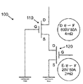
図2は、本発明に従って構成される回路100の一例を示す。GaNベースのデプレッションモードFET 110のソースが、エンハンスメントモードFET 120のドレインに接続される。エンハンスメントモードFET 120は例えば、一般に入手可能なシリコンまたはGaAsベースのデバイスであることができる。FET 110が常にオンであるように、デプレッションモードFET 110のゲートが接地される。図2の例ではFET 120のオン状態は、FET 110のゲートを接地に接続することによって維持される。エンハンスメントモードFET 120のソースは、接地される。デプレッションモードFET 110のドレインは、回路100のドレインDとして機能する。エンハンスメントモードFET 120のソースは、回路100のソースSとして機能する。同様に、エンハンスメントモードFET 120のゲートは回路100のゲートGとして機能する。
FIG. 2 shows an example of a
回路100の動作は、図3および4内に示される電流−電圧特性曲線を参照して説明されることができる。説明だけのためにかつ本発明の限定ではなく、両方のFET 110および120はn型であるが、しかし、代わりとしてp型デバイスが同様に使われることができる。図3は、エンハンスメントモードFET 120の電流対ゲート−ソース電圧を示す。この例では、FET 120のピンチオフ電圧が5Vであることを示す。図4は、デプレッションモードFET 110の電流対ゲート−ソース電圧を示す。この例ではデプレッションモードFET 110のピンチオフ電圧が、−6Vであることを示す。
The operation of
図4は、ゲート−ソース間電圧VGSが0V以上の場合、デプレッションモードFET 110がオン状態のままであることを示す。示された例においてFET 110のゲートが接地されているので、デプレッションモードFETは常にオンである。図3は、5V以上のゲート−ソース間電圧VGSが印加される場合、エンハンスメントモードFET 120が常にオンであることを示す。電流がデプレッションモードFET 110のドレインDからエンハンスメントモードFET 120のソースSへの経路に沿って流れる必要があるので、回路がゲート電圧Gを5V以上の値に変えることによってそのオン状態になり、それによってエンハンスメントモードFETのように働く。このようにしてエンハンスメントモードFET 120のゲートGは、回路100中の電流をエンハンスメントモードFETのように調節し、一方デプレッションモードFET 110のブロッキング電圧が回路100全体のブロッキング能力を与える。回路100は、したがって、600VのGaNベースエンハンスメントモードFETのように働く。図5は、回路100の電流対ゲート−ソース電圧を示す。
FIG. 4 shows that the
上に提示された例において、GaNベースのデプレッションモードFET 110は600Vの電圧定格を有し、および、FET 120の電圧定格は20Vである。さらに一般的にいえば、本発明のいくつかの実施態様において、デプレッションモードFETは任意の適切な高電圧(例えば約100 Vより大きいV)FETである。回路100の出力電圧は、デプレッションモードFET 110とエンハンスメントモードFET 120との間の電圧定格の差に概ね等しい。したがって、回路100の電圧定格を最大化するために、エンハンスメントモードFET 120の電圧定格は好ましくはできるだけ低く選ばれる。例えば、その電流定格およびオン状態でのそのドレイン−ソース抵抗のような回路100の残りの特性は、デプレッションモードFET 110のそれらと類似している。
In the example presented above, the GaN based
図6−8は、回路100内に使用されることができるデプレッションモードFET 110のいくつかの特定の例を示す。もちろん、本発明はこれらの構造に限られず、それは説明の目的のみに示されている。図6において、デプレッションモードFET10は基板12、核形成(遷移)層18、GaN緩衝層22、アルミニウム窒化ガリウム(AlxGa1−xN;0<X<1)ショットキ層24およびキャップまたは終端層16を含む。更に、FET10はソースコンタクト27、ゲートコンタクト28およびドレインコンタクト30を含む。
6-8 show some specific examples of
FET10は、一般的にエピタキシャル成長プロセスを使用して、製造される。たとえば、ガリウム、アルミニウムおよび/またはインジウムのような、半導体の金属成分が、ターゲットおよび基板の双方が、窒素および一つ以上のドーパントを含むガスの雰囲気内にある間、基板に極めて近傍に配設された金属ターゲットから叩き出されるところで反応性スパッタリングプロセスが、使われることができる。代わりとして、金属有機化学蒸着(MOCVD)が使用されることができ、基板が高い温度、一般的に約700−1100℃に維持される間、基板が、金属の有機化合物を含む雰囲気に、同じくアンモニアのような反応性窒素含有ガスおよびドーパント含有ガスに曝露される。ガス状の化合物が、分解して、基板302の表面の上に結晶材料のフィルムの形のドープされた半導体を形成する。基板および成長されたフィルムは、次いで冷却される。更なる変形例として、分子線エピタキシ(MBE)または原子層エピタキシのような他のエピタキシャル成長方法が使われることができる。使用されることができるさらに追加的な技術としては、流量変調有機金属化合物気相成長(FM−OMVPE)、有機金属化合物気相成長(OMVPE)、水素化物気相成長(HVPE)および物理蒸着法(PVD)が挙げられるが、これに限定されるものではない。
The
構造の成長を開始するために、核形成層18が基板12上に付着される。基板12は、サファイヤまたは炭化珪素(SiC)を含むがこれに限らずさまざまな材料から形成されることができる。核形成層18は例えば、AlxGa1−xNのようなアルミニウムに富む層であることができ、ここでXは0から1までの範囲内にある。核形成層18はGaN緩衝層22と基板12との間の格子不整合を補正するように働く。一般に、1つの層の原子間の間隔が隣接層の原子間の間隔に整合しないときに、格子不整合が作り出される。格子不整合の結果として、隣接層の原子間の結合は弱く、および、隣接層に亀裂が入るか、分かれるかまたは多数の結晶欠陥を有する可能性がある。したがって、核形成層18は基板12の結晶構造とGaN緩衝層22の結晶構造との間に界面を作り出すことによってGaN緩衝層22と基板12との間の格子不整合を補正するように働く。
A
核形成層18を付着したあと、GaN緩衝層22が核形成層18上に付着され、および、AlxGa1−xNショットキ層24がGaN緩衝層22上に付着される。薄い、高移動度チャンネルである二次元伝導チャンネル26が、キャリヤをGaN緩衝層22とAlxGa1−xNショットキ層24との間の界面領域に限定する。キャップまたは終端層16が、AlxGa1−xNショットキ層24上に付着されて、FET10の製造および動作中に、AlxGa1−xNショットキ層24を酸化のような表面反応から保護するように働く。ショットキ層24がアルミニウムを含むので、AlxGa1−xNショットキ層24が大気に曝露されて、別な方法で保護されていない場合、酸化が生じる。
After depositing the
基板12上のエピタキシャル層18、22および24ならびに終端層16の成長の後、FET10は、終端層16上に、それぞれソース、ゲートおよびドレインコンタクト27、28および30を付着することによって完成される。コンタクト27、28および30の各々は、金属コンタクトである。好ましくは、ゲートコンタクト28はニッケル、金のような、しかしこれに限られない金属材料であり、ならびにソースおよびドレインコンタクト27および30は、各々、チタン、金またはアルミニウムのような、しかしこれらに限られない金属材料である。
After growth of
本発明の一実施態様において、終端層16はAlxGa1−xNショットキ層24上に形成されるInGaN層である。InGaN層16は、2つの目的を果たし、その第1は、酸化が減少されるように、Alを含まない上層を提供することである。さらに、InGaAlNのようなAl含有化合物が、適切な均一性および平滑性を提供するために一般により高い成長温度が必要なので、Alを含む材料の代わりにInGaN材料を用いて、成長プロセスが単純化されることができる。加えて、InGaN層24は表面でポテンシャルバリアをわずかに低下させ、それが表面電荷の蓄積を減少させることができて、この構造の表面上のリーク電流を減少させることができる。
In one embodiment of the present invention, the
本発明の別の実施態様において、終端層16はAl金属を備えたフラッシュ層である。フラッシュ層は、材料のきわめて短いバーストで形成されている。これは、構造の表面の上にきわめて薄い(例えば1−2単分子層の材料)、しかし、平坦なカバレージを形成する。フラッシュ層は、一般にその場で施される。金属Alが形成され、かつAlNが形成されないことを確実にするために、AlNを形成するときにさもなければ存在するであろう反応性窒素含有ガス(例えばアンモニア)が、不在である。Alフラッシュ層は、高いかまたは低い温度で形成されることができる。その形成の後、Alはその後アニールされて薄い酸化物層を形成することができる。Alフラッシュ層がきわめて薄いので、それはその全体に酸化されることができ、したがって、材料の上に初期「自然」酸化膜を作り出し、それは、次いでショットキ層24をプロセスでしばしば見られるタイプの劣化を受けることから保護する。これは、また、その両方がHEMT性能にとって重要な、リーク電流の減少および降伏電圧増大のための追加的なバリア材料として働くことができる。Alの代わりに、フラッシュ層はガリウムまたはさらにインジウムのような他の金属を備えることができる。GaまたはInフラッシュ層は、また、構造上に均一な「自然」酸化膜を形成するために酸化されることができる。
In another embodiment of the present invention,
本発明のさらに他の実施態様において、キャップまたは終端層16が高度にFeドープされたGaN、SiドープされたGaN、FeNまたはSiNのようなその他の材料から形成されることができる。エピタキシャル、非エピタキシャルまたはアモルファスでさえあることができるこれらの層は、初期不活性化層として、または、リーク電流を減少させ、かつ降伏電圧を増大する追加的なバリア材料として、機能することができる。たとえば、FeのGaNへの追加は、材料がより絶縁性となり、電子移動度を減少させるので、リーク電流を減少させることができる材料になる。
In still other embodiments of the invention, the cap or
本発明の他の実施態様において、薄いAlN層がAlxGa1−xNショットキ層24上に形成されることができる。この層は、より効率的に電荷を調節するのを助けるために追加的なショットキバリア層を提供し、したがって、デバイスのリーク電流を減少させて、降伏電圧を増大する。AlNはオーミックコンタクトを付着するために容易にウエットエッチングすることができるので、AlN層はまた構造の初期不活性化層として働くことができる。代わりとして、不活性化層を形成するためにAlN層が酸化されることができる。
In other embodiments of the present invention, a thin AlN layer can be formed on the Al x Ga 1-x
いくつかの実施態様において、終端層16はおよそ1ないし5ナノメートルの厚さである。したがって、電子は終端層16中を容易にトンネルすることができる。結果として、終端層16はゲートコンタクト28とAlxGa1−xNショットキ層24との間のショットキバリア高さを増加させず、ここでショットキバリア高さはゲートコンタクト28とAlxGa1−xNショットキ層24との界面における電子によって直面されるポテンシャルエネルギーバリアを規定する。更に、終端層16はソースおよびドレインコンタクト27および30の形成に影響を及ぼさない。
In some embodiments,
図7は、FET10のさらに別の実施態様を示し、そこにおいてオーミックコンタクト27および28が、AlxGa1−xNショットキ層24から形成される凹部内に位置する。この凹部は、従来の技術に従ってAlxGa1−xNショットキ層24をエッチングすることによって形成される。凹部は、AlxGa1−xNショットキ層24を通して部分的にまたは完全に延伸することができる。たとえば、場合によっては、凹部は深さ約5ないし15nmの深さまで延伸することができ、それによってAlxGa1−xNショットキ層24の充分な厚さがチャンネル層26を作り出すままとすることを可能にする。このようにコンタクトをへこませることによってコンタクト比抵抗および表面の平滑性が、オーミックコンタクトを形成するために付着される金属の浸透を増加させるように減少される。増大された表面粗さは、半導体内へのより良い金属のマイグレーションに結びつく)。低オン抵抗を必要とするデバイスに対して、この配置は最も低い可能なオン抵抗を達成する点で有意であることができる。図示されてはいないが、本発明の本実施態様はまた、上で論じられたもののようなキャップまたは終端層を使用することができる。この場合、コンタクト27および28が位置する凹部はまた、終端層を通して延伸する。
FIG. 7 shows yet another embodiment of the
図8は、バリア層24がAlxGa1−xNの代わりにAlInGaNから形成されるFET10の別の実施態様を示す。たとえば、(非特許文献1)内に論じられているように、xが0.1から0.2まで、およびyが0.00から0.02まで変化する合金組成を有する50nm未満のバリア厚さを有するAlxInyGa(1−x−y)N接合が、使用される。さらに、Khan他は、格子定数の直線補間に基づいて、Al/In比率5がほぼGaNと格子整合するべきであると述べている。AlInGaNを用いて、歪がバンドギャップから独立に制御されることができ、それによって、材料のバンドギャップが臨界厚に関しより自由に変更されることができる。パワーデバイスに対してこれは、不必要に材料に応力を加えて、材料が時間とともに弛緩するにつれてさもなければ生じるであろう、デバイス寿命を減少させることなく、チャンネル内にほとんどの電荷を得るために決定的となることができる。
FIG. 8 shows another embodiment of the
さまざまな実施態様が詳細に例示されて、本願明細書において記載されているとはいえ、理解されるであろうことは、本発明の修正および変更が、上記の教示によって包含され、かつ本発明の趣旨および意図された目的から逸脱することなく、添付の特許請求の範囲の範囲内にある、ということである。例えば、デプレッションモードFETがGaNベースのデバイスとして記述されたとはいえ、本発明は、さらに一般的にいえばIII属元素がガリウム(Ga)、アルミニウム(Al)、硼素(B)またはインジウム(In)であることができる任意のIII属窒化物化合物半導体から形成されるデプレッションモードFETを包含する。 Although various embodiments have been illustrated in detail and described herein, it will be understood that modifications and variations of the present invention are encompassed by the above teachings and the present invention. And within the scope of the appended claims without departing from the spirit and intended purpose thereof. For example, although a depletion mode FET has been described as a GaN-based device, the present invention more generally refers to the group III elements gallium (Ga), aluminum (Al), boron (B) or indium (In). Depletion mode FETs formed from any Group III nitride compound semiconductor that can be
10 デプレッションモードFET
12 基板
16 終端層
18 核形成層
22 緩衝層
24 ショットキ層
26 チャンネル層
27 ソースコンタクト
28 ゲートコンタクト
30 ドレインコンタクト
91 半絶縁基板
92 緩衝層
93 ドープされていないGaN層
94 ドープされていないAlGaN層
95 コンタクト層
96 電子ガス
100 回路
110 デプレッションモードFET
120 エンハンスメントモードFET
302 基板
10 Depletion mode FET
12
91
100
120 enhancement mode FET
302 substrate
Claims (17)
入力ドレイン、ソースおよびゲートノードと、
ソース、ドレインおよびゲートを有するIII属窒素化合物デプレッションモードFETであって、前記デプレッションモードFETの前記ゲートが、前記デプレッションモードFETをそのオン状態に維持する電位に連結される、FETと、
ソース、ドレインおよびゲートを有するエンハンスメントモードFETであって、前記デプレッションモードFETの前記ソースが、前記エンハンスメントモードFETの前記ドレインに直列に連結されるFETと、を備え、そして、
前記デプレッションモードFETの前記ドレインが前記入力ドレインノードとして機能し、前記エンハンスメントモードFETの前記ソースが前記入力ソースノードとして機能し、および、前記エンハンスメントモードFETの前記ゲートが前記入力ゲートノードとして機能し、
前記III属窒素化合物デプレッションモードFETが、
基板と、
前記基板の上に配設される第1の活性層と、
前記第1の活性層上に配設される第2の活性層であって、二次元の電子ガス層が前記第1の活性層と前記第2の活性層との間に生じるように、前記第1の活性層より大きいバンドギャップを有する第2の活性層と、
前記第2の活性層上に配設されるフラッシュ層と、
前記フラッシュ層上に配設されるソース、ゲートおよびドレインコンタクトと、を備え 前記デプレッションモードFETが、約100Vより大きい電圧定格を有する高電圧FETであり、
前記エンハンスメントモードFETはシリコンベース又はGaAsベースのデバイスであって、広バンドギャップの半導体デバイスではない、
ことを特徴とする回路。 A circuit,
Input drain, source and gate nodes;
A Group III nitrogen compound depletion mode FET having a source, a drain, and a gate, wherein the gate of the depletion mode FET is coupled to a potential that maintains the depletion mode FET in its on state; and
An enhancement mode FET having a source, a drain, and a gate, wherein the source of the depletion mode FET is coupled in series with the drain of the enhancement mode FET; and
The drain of the depletion mode FET functions as the input drain node, the source of the enhancement mode FET functions as the input source node, and the gate of the enhancement mode FET functions as the input gate node;
The group III nitrogen compound depletion mode FET is
A substrate,
A first active layer disposed on the substrate;
A second active layer disposed on the first active layer, wherein a two-dimensional electron gas layer is formed between the first active layer and the second active layer; A second active layer having a larger band gap than the first active layer;
A flash layer disposed on the second active layer;
Source disposed on said flash layer, and the gate and drain contacts, said depletion mode FET provided with, Ri high voltage FET der with about 100V larger voltage rating,
The enhancement mode FET is a silicon or GaAs based device, not a wide bandgap semiconductor device,
A circuit characterized by that.
前記第2の活性層がその中に形成される第1および第2の凹部を含み、
前記ソースおよびドレインコンタクトが、前記第1および第2の凹部内にそれぞれ配設されている、
ことを特徴とする回路。 The circuit of claim 1, comprising:
The second active layer includes first and second recesses formed therein;
The source and drain contacts are disposed in the first and second recesses, respectively.
A circuit characterized by that.
入力ドレイン、ソースおよびゲートノードと、
III属窒素化合物デプレッションモードFETと、
前記デプレッションモードFETと直列に配置されるエンハンスメントモードFETと、を備え、そして、
前記デプレッションモードFETの第1の端子が前記入力ドレインノードとして機能し、および、前記エンハンスメントモードFETの第2のおよび第3の端子がそれぞれ、前記ソースおよびゲートノードとして機能し、
前記III属窒素化合物デプレッションモードFETが、
基板と、
前記基板の上に配設される第1の活性層と、
前記第1の活性層上に配設される第2の活性層であって、二次元の電子ガス層が前記第1の活性層と前記第2の活性層との間に生じるように、前記第1の活性層より大きいバンドギャップを有する第2の活性層と、
前記第2の活性層上に配設されるフラッシュ層と、
前記フラッシュ層上に配設されるソース、ゲートおよびドレインコンタクトと、を備え 前記デプレッションモードFETが、約100Vより大きい電圧定格を有する高電圧FETであり、
前記エンハンスメントモードFETはシリコンベース又はGaAsベースのデバイスであって、広バンドギャップの半導体デバイスではない、
ことを特徴とする回路。 A circuit,
Input drain, source and gate nodes;
Group III nitrogen compound depletion mode FET;
An enhancement mode FET arranged in series with the depletion mode FET, and
A first terminal of the depletion mode FET functions as the input drain node, and a second and third terminal of the enhancement mode FET function as the source and gate nodes, respectively;
The group III nitrogen compound depletion mode FET is
A substrate,
A first active layer disposed on the substrate;
A second active layer disposed on the first active layer, wherein a two-dimensional electron gas layer is formed between the first active layer and the second active layer; A second active layer having a larger band gap than the first active layer;
A flash layer disposed on the second active layer;
Source, gate and drain contacts disposed on the flash layer, wherein the depletion mode FET is a high voltage FET having a voltage rating greater than about 100V;
The enhancement mode FET is a silicon or GaAs based device, not a wide bandgap semiconductor device,
A circuit characterized by that.
前記第2の活性層がその中に形成される第1および第2の凹部を含み、
前記ソースおよびドレインコンタクトが前記第1および第2の凹部内にそれぞれ配設されている、
ことを特徴とする回路。 14. The circuit of claim 13, comprising
The second active layer includes first and second recesses formed therein;
The source and drain contacts are respectively disposed in the first and second recesses;
A circuit characterized by that.
Applications Claiming Priority (3)
| Application Number | Priority Date | Filing Date | Title |
|---|---|---|---|
| US11/725,760 US7501670B2 (en) | 2007-03-20 | 2007-03-20 | Cascode circuit employing a depletion-mode, GaN-based FET |
| US11/725,760 | 2007-03-20 | ||
| PCT/US2008/057593 WO2008116038A2 (en) | 2007-03-20 | 2008-03-20 | Cascode circuit employing a depletion-mode, gan-based fet |
Related Child Applications (1)
| Application Number | Title | Priority Date | Filing Date |
|---|---|---|---|
| JP2014142832A Division JP2014209659A (en) | 2007-03-20 | 2014-07-11 | CASCODE CIRCUIT EMPLOYING DEPLETION-MODE GaN-BASED FET |
Publications (2)
| Publication Number | Publication Date |
|---|---|
| JP2010522432A JP2010522432A (en) | 2010-07-01 |
| JP5580602B2 true JP5580602B2 (en) | 2014-08-27 |
Family
ID=39766758
Family Applications (2)
| Application Number | Title | Priority Date | Filing Date |
|---|---|---|---|
| JP2009554725A Expired - Fee Related JP5580602B2 (en) | 2007-03-20 | 2008-03-20 | Cascode circuit using depletion mode GaN-based FET |
| JP2014142832A Pending JP2014209659A (en) | 2007-03-20 | 2014-07-11 | CASCODE CIRCUIT EMPLOYING DEPLETION-MODE GaN-BASED FET |
Family Applications After (1)
| Application Number | Title | Priority Date | Filing Date |
|---|---|---|---|
| JP2014142832A Pending JP2014209659A (en) | 2007-03-20 | 2014-07-11 | CASCODE CIRCUIT EMPLOYING DEPLETION-MODE GaN-BASED FET |
Country Status (7)
| Country | Link |
|---|---|
| US (1) | US7501670B2 (en) |
| EP (1) | EP2140497A4 (en) |
| JP (2) | JP5580602B2 (en) |
| KR (1) | KR101497725B1 (en) |
| CN (2) | CN101689570B (en) |
| HK (1) | HK1142996A1 (en) |
| WO (1) | WO2008116038A2 (en) |
Families Citing this family (88)
| Publication number | Priority date | Publication date | Assignee | Title |
|---|---|---|---|---|
| FR2914500B1 (en) * | 2007-03-30 | 2009-11-20 | Picogiga Internat | IMPROVED OHMICALLY CONTACT ELECTRONIC DEVICE |
| JP2008306130A (en) * | 2007-06-11 | 2008-12-18 | Sanken Electric Co Ltd | Field-effect semiconductor device and its manufacturing method |
| US7915643B2 (en) | 2007-09-17 | 2011-03-29 | Transphorm Inc. | Enhancement mode gallium nitride power devices |
| US7965126B2 (en) * | 2008-02-12 | 2011-06-21 | Transphorm Inc. | Bridge circuits and their components |
| US8519438B2 (en) | 2008-04-23 | 2013-08-27 | Transphorm Inc. | Enhancement mode III-N HEMTs |
| US8289065B2 (en) | 2008-09-23 | 2012-10-16 | Transphorm Inc. | Inductive load power switching circuits |
| US7898004B2 (en) | 2008-12-10 | 2011-03-01 | Transphorm Inc. | Semiconductor heterostructure diodes |
| US7884394B2 (en) * | 2009-02-09 | 2011-02-08 | Transphorm Inc. | III-nitride devices and circuits |
| JP5562579B2 (en) * | 2009-05-12 | 2014-07-30 | 日本碍子株式会社 | Method for producing epitaxial substrate for semiconductor device |
| US8742459B2 (en) | 2009-05-14 | 2014-06-03 | Transphorm Inc. | High voltage III-nitride semiconductor devices |
| US7915645B2 (en) * | 2009-05-28 | 2011-03-29 | International Rectifier Corporation | Monolithic vertically integrated composite group III-V and group IV semiconductor device and method for fabricating same |
| TW201103150A (en) * | 2009-07-10 | 2011-01-16 | Tekcore Co Ltd | Group III-nitride semiconductor Schottky diode and its fabrication method |
| US7939857B1 (en) * | 2009-08-24 | 2011-05-10 | Itt Manufacturing Enterprises, Inc. | Composite device having three output terminals |
| US20110049580A1 (en) * | 2009-08-28 | 2011-03-03 | Sik Lui | Hybrid Packaged Gate Controlled Semiconductor Switching Device Using GaN MESFET |
| US8390000B2 (en) | 2009-08-28 | 2013-03-05 | Transphorm Inc. | Semiconductor devices with field plates |
| US8389977B2 (en) | 2009-12-10 | 2013-03-05 | Transphorm Inc. | Reverse side engineered III-nitride devices |
| US8802516B2 (en) * | 2010-01-27 | 2014-08-12 | National Semiconductor Corporation | Normally-off gallium nitride-based semiconductor devices |
| CN101783666B (en) * | 2010-02-11 | 2012-07-04 | 西安科技大学 | Reinforced-depletion-mode part combination switch circuit capable of being reliably turned off |
| US9219058B2 (en) * | 2010-03-01 | 2015-12-22 | Infineon Technologies Americas Corp. | Efficient high voltage switching circuits and monolithic integration of same |
| US8981380B2 (en) | 2010-03-01 | 2015-03-17 | International Rectifier Corporation | Monolithic integration of silicon and group III-V devices |
| US8742460B2 (en) | 2010-12-15 | 2014-06-03 | Transphorm Inc. | Transistors with isolation regions |
| US8643062B2 (en) | 2011-02-02 | 2014-02-04 | Transphorm Inc. | III-N device structures and methods |
| US8896131B2 (en) | 2011-02-03 | 2014-11-25 | Alpha And Omega Semiconductor Incorporated | Cascode scheme for improved device switching behavior |
| US8847408B2 (en) * | 2011-03-02 | 2014-09-30 | International Rectifier Corporation | III-nitride transistor stacked with FET in a package |
| US8716141B2 (en) | 2011-03-04 | 2014-05-06 | Transphorm Inc. | Electrode configurations for semiconductor devices |
| US8772842B2 (en) | 2011-03-04 | 2014-07-08 | Transphorm, Inc. | Semiconductor diodes with low reverse bias currents |
| US9859882B2 (en) * | 2011-03-21 | 2018-01-02 | Infineon Technologies Americas Corp. | High voltage composite semiconductor device with protection for a low voltage device |
| US9236376B2 (en) | 2011-03-21 | 2016-01-12 | Infineon Technologies Americas Corp. | Power semiconductor device with oscillation prevention |
| US8766375B2 (en) * | 2011-03-21 | 2014-07-01 | International Rectifier Corporation | Composite semiconductor device with active oscillation prevention |
| US9362905B2 (en) * | 2011-03-21 | 2016-06-07 | Infineon Technologies Americas Corp. | Composite semiconductor device with turn-on prevention control |
| US8987833B2 (en) | 2011-04-11 | 2015-03-24 | International Rectifier Corporation | Stacked composite device including a group III-V transistor and a group IV lateral transistor |
| US9343440B2 (en) | 2011-04-11 | 2016-05-17 | Infineon Technologies Americas Corp. | Stacked composite device including a group III-V transistor and a group IV vertical transistor |
| US8710511B2 (en) | 2011-07-29 | 2014-04-29 | Northrop Grumman Systems Corporation | AIN buffer N-polar GaN HEMT profile |
| US8901604B2 (en) | 2011-09-06 | 2014-12-02 | Transphorm Inc. | Semiconductor devices with guard rings |
| US9257547B2 (en) | 2011-09-13 | 2016-02-09 | Transphorm Inc. | III-N device structures having a non-insulating substrate |
| US8598937B2 (en) | 2011-10-07 | 2013-12-03 | Transphorm Inc. | High power semiconductor electronic components with increased reliability |
| JP2013153027A (en) * | 2012-01-24 | 2013-08-08 | Fujitsu Ltd | Semiconductor device and power supply device |
| US9165766B2 (en) | 2012-02-03 | 2015-10-20 | Transphorm Inc. | Buffer layer structures suited for III-nitride devices with foreign substrates |
| WO2013155108A1 (en) | 2012-04-09 | 2013-10-17 | Transphorm Inc. | N-polar iii-nitride transistors |
| US9184275B2 (en) | 2012-06-27 | 2015-11-10 | Transphorm Inc. | Semiconductor devices with integrated hole collectors |
| US8803246B2 (en) * | 2012-07-16 | 2014-08-12 | Transphorm Inc. | Semiconductor electronic components with integrated current limiters |
| US8933461B2 (en) * | 2012-08-09 | 2015-01-13 | Texas Instruments Incorporated | III-nitride enhancement mode transistors with tunable and high gate-source voltage rating |
| KR101919421B1 (en) | 2012-08-16 | 2018-11-19 | 삼성전자주식회사 | Semiconductor device and method of manufacturing the same |
| KR101922117B1 (en) | 2012-08-16 | 2018-11-26 | 삼성전자주식회사 | Electronic device including transistor and method of operating the same |
| US9438112B2 (en) * | 2012-08-23 | 2016-09-06 | Infineon Technologies Americas Corp. | Power converter including integrated driver for depletion mode group III-V transistor |
| WO2014034346A1 (en) * | 2012-08-28 | 2014-03-06 | シャープ株式会社 | Composite semiconductor device |
| ITTO20121081A1 (en) * | 2012-12-14 | 2014-06-15 | St Microelectronics Srl | ELECTRONIC POWER COMPONENT NORMALLY OFF |
| CN105164811B (en) | 2013-02-15 | 2018-08-31 | 创世舫电子有限公司 | Electrode of semiconductor devices and forming method thereof |
| US9087718B2 (en) | 2013-03-13 | 2015-07-21 | Transphorm Inc. | Enhancement-mode III-nitride devices |
| US9245993B2 (en) | 2013-03-15 | 2016-01-26 | Transphorm Inc. | Carbon doping semiconductor devices |
| US9443938B2 (en) | 2013-07-19 | 2016-09-13 | Transphorm Inc. | III-nitride transistor including a p-type depleting layer |
| US9007117B2 (en) | 2013-08-02 | 2015-04-14 | Infineon Technologies Dresden Gmbh | Solid-state switching device having a high-voltage switching transistor and a low-voltage driver transistor |
| WO2015033631A1 (en) * | 2013-09-06 | 2015-03-12 | シャープ株式会社 | Transistor circuit |
| JP6237038B2 (en) * | 2013-09-20 | 2017-11-29 | 富士通株式会社 | Cascode transistor and control method of cascode transistor |
| US9525063B2 (en) | 2013-10-30 | 2016-12-20 | Infineon Technologies Austria Ag | Switching circuit |
| US9048838B2 (en) | 2013-10-30 | 2015-06-02 | Infineon Technologies Austria Ag | Switching circuit |
| US9257424B2 (en) | 2013-11-08 | 2016-02-09 | Infineon Technologies Austria Ag | Semiconductor device |
| CN110166033B (en) * | 2013-11-15 | 2023-07-07 | 德克萨斯仪器股份有限公司 | Method and circuit for controlling depletion transistor |
| US9325308B2 (en) * | 2014-05-30 | 2016-04-26 | Delta Electronics, Inc. | Semiconductor device and cascode circuit |
| US9318593B2 (en) | 2014-07-21 | 2016-04-19 | Transphorm Inc. | Forming enhancement mode III-nitride devices |
| CN104201202B (en) * | 2014-09-17 | 2017-01-25 | 电子科技大学 | Gallium-nitride-based heterostructure field effect transistor with composite barrier layers |
| US9536966B2 (en) | 2014-12-16 | 2017-01-03 | Transphorm Inc. | Gate structures for III-N devices |
| US9536967B2 (en) | 2014-12-16 | 2017-01-03 | Transphorm Inc. | Recessed ohmic contacts in a III-N device |
| WO2016185745A1 (en) | 2015-05-15 | 2016-11-24 | シャープ株式会社 | Composite semiconductor device |
| US9748941B2 (en) | 2015-10-27 | 2017-08-29 | Electronics And Telecommunications Research Institute | Power semiconductor module and method for stabilizing thereof |
| KR102265460B1 (en) | 2016-01-11 | 2021-06-16 | 한국전자통신연구원 | Cascode Switch Circuit |
| US11322599B2 (en) | 2016-01-15 | 2022-05-03 | Transphorm Technology, Inc. | Enhancement mode III-nitride devices having an Al1-xSixO gate insulator |
| JP6061047B1 (en) | 2016-03-16 | 2017-01-18 | 富士電機株式会社 | Semiconductor device |
| US9929261B2 (en) | 2016-04-07 | 2018-03-27 | Semiconductor Components Industries, Llc | Electronic device including a HEMT with a segmented gate electrode |
| US10128232B2 (en) | 2016-05-20 | 2018-11-13 | Synopsys, Inc. | Heterojunction field effect transistor device with serially connected enhancement mode and depletion mode gate regions |
| US10224401B2 (en) | 2016-05-31 | 2019-03-05 | Transphorm Inc. | III-nitride devices including a graded depleting layer |
| US9865721B1 (en) * | 2016-06-15 | 2018-01-09 | Qorvo Us, Inc. | High electron mobility transistor (HEMT) device and method of making the same |
| US9871510B1 (en) | 2016-08-24 | 2018-01-16 | Power Integrations, Inc. | Clamp for a hybrid switch |
| US10256811B2 (en) | 2016-11-22 | 2019-04-09 | Electronics And Telecommunications Research Institute | Cascode switch circuit including level shifter |
| GB2565805B (en) | 2017-08-23 | 2020-05-13 | X Fab Semiconductor Foundries Gmbh | Noff III-nitride high electron mobility transistor |
| US10777638B1 (en) | 2018-01-04 | 2020-09-15 | Synopsys, Inc. | Constricted junctionless FinFET/nanowire/nanosheet device having cascode portion |
| US10840798B1 (en) | 2018-09-28 | 2020-11-17 | Dialog Semiconductor (Uk) Limited | Bidirectional signaling method for high-voltage floating circuits |
| US11139290B2 (en) * | 2018-09-28 | 2021-10-05 | Taiwan Semiconductor Manufacturing Company, Ltd. | High voltage cascode HEMT device |
| CN111199958A (en) * | 2018-11-16 | 2020-05-26 | 苏州东微半导体有限公司 | Semiconductor power device |
| US11211484B2 (en) | 2019-02-13 | 2021-12-28 | Monolithic Power Systems, Inc. | Vertical transistor structure with buried channel and resurf regions and method of manufacturing the same |
| US11088688B2 (en) | 2019-02-13 | 2021-08-10 | Logisic Devices, Inc. | Configurations of composite devices comprising of a normally-on FET and a normally-off FET |
| US10991722B2 (en) | 2019-03-15 | 2021-04-27 | International Business Machines Corporation | Ultra low parasitic inductance integrated cascode GaN devices |
| TWI761704B (en) * | 2019-09-12 | 2022-04-21 | 黃知澍 | Ga-face group III/nitride epitaxial structure and its active device and its gate protection device |
| US11127848B2 (en) * | 2019-11-29 | 2021-09-21 | Vanguard International Semiconductor Corporation | Semiconductor structure and method for forming the same |
| TWI775027B (en) * | 2019-12-20 | 2022-08-21 | 世界先進積體電路股份有限公司 | Semiconductor structure |
| US11152364B1 (en) | 2020-04-21 | 2021-10-19 | Vanguard International Semiconductor Corporation | Semiconductor structure and methods for manufacturing the same |
| CN116344595A (en) * | 2023-03-03 | 2023-06-27 | 天狼芯半导体(成都)有限公司 | Gallium nitride semiconductor device and method for manufacturing gallium nitride semiconductor device |
| CN117155359B (en) * | 2023-10-26 | 2024-02-09 | 深圳智芯微电子科技有限公司 | Pretreatment method of GaN HEMT device |
Family Cites Families (14)
| Publication number | Priority date | Publication date | Assignee | Title |
|---|---|---|---|---|
| JPH0789586B2 (en) * | 1986-09-01 | 1995-09-27 | 株式会社日立製作所 | Semiconductor device |
| JP4751498B2 (en) * | 2000-03-30 | 2011-08-17 | 富士通株式会社 | Semiconductor three-terminal device |
| WO2004061923A1 (en) * | 2002-12-27 | 2004-07-22 | General Electric Company | Gallium nitride crystal, homoepitaxial gallium-nitride-based devices and method for producing same |
| JP2004247709A (en) * | 2003-01-22 | 2004-09-02 | Matsushita Electric Ind Co Ltd | Semiconductor device and manufacturing method therefor |
| EP1665358B1 (en) * | 2003-09-09 | 2020-07-01 | The Regents of The University of California | Fabrication of single or multiple gate field plates |
| TWI258798B (en) * | 2003-12-05 | 2006-07-21 | Int Rectifier Corp | III-nitride device passivation and method |
| US7465997B2 (en) * | 2004-02-12 | 2008-12-16 | International Rectifier Corporation | III-nitride bidirectional switch |
| US7202528B2 (en) * | 2004-12-01 | 2007-04-10 | Semisouth Laboratories, Inc. | Normally-off integrated JFET power switches in wide bandgap semiconductors and methods of making |
| US7119380B2 (en) | 2004-12-01 | 2006-10-10 | Semisouth Laboratories, Inc. | Lateral trench field-effect transistors in wide bandgap semiconductor materials, methods of making, and integrated circuits incorporating the transistors |
| JP2006190991A (en) * | 2004-12-09 | 2006-07-20 | Matsushita Electric Ind Co Ltd | Field effect transistor and its manufacturing method |
| US7405430B2 (en) * | 2005-06-10 | 2008-07-29 | Cree, Inc. | Highly uniform group III nitride epitaxial layers on 100 millimeter diameter silicon carbide substrates |
| JP4645313B2 (en) * | 2005-06-14 | 2011-03-09 | 富士電機システムズ株式会社 | Semiconductor device |
| JP4897948B2 (en) * | 2005-09-02 | 2012-03-14 | 古河電気工業株式会社 | Semiconductor element |
| US8264003B2 (en) * | 2006-03-20 | 2012-09-11 | International Rectifier Corporation | Merged cascode transistor |
-
2007
- 2007-03-20 US US11/725,760 patent/US7501670B2/en active Active
-
2008
- 2008-03-20 KR KR1020097021925A patent/KR101497725B1/en not_active IP Right Cessation
- 2008-03-20 EP EP08744097A patent/EP2140497A4/en not_active Withdrawn
- 2008-03-20 CN CN2008800090640A patent/CN101689570B/en active Active
- 2008-03-20 WO PCT/US2008/057593 patent/WO2008116038A2/en active Application Filing
- 2008-03-20 CN CN201210189604.6A patent/CN102694013B/en active Active
- 2008-03-20 JP JP2009554725A patent/JP5580602B2/en not_active Expired - Fee Related
-
2010
- 2010-09-29 HK HK10109342.4A patent/HK1142996A1/en not_active IP Right Cessation
-
2014
- 2014-07-11 JP JP2014142832A patent/JP2014209659A/en active Pending
Also Published As
| Publication number | Publication date |
|---|---|
| JP2014209659A (en) | 2014-11-06 |
| WO2008116038A3 (en) | 2008-11-20 |
| US7501670B2 (en) | 2009-03-10 |
| CN102694013B (en) | 2015-08-12 |
| EP2140497A2 (en) | 2010-01-06 |
| KR20100015747A (en) | 2010-02-12 |
| KR101497725B1 (en) | 2015-03-04 |
| JP2010522432A (en) | 2010-07-01 |
| CN101689570A (en) | 2010-03-31 |
| CN101689570B (en) | 2012-06-27 |
| CN102694013A (en) | 2012-09-26 |
| US20080230784A1 (en) | 2008-09-25 |
| HK1142996A1 (en) | 2010-12-17 |
| WO2008116038A2 (en) | 2008-09-25 |
| EP2140497A4 (en) | 2011-09-21 |
Similar Documents
| Publication | Publication Date | Title |
|---|---|---|
| JP5580602B2 (en) | Cascode circuit using depletion mode GaN-based FET | |
| US7939853B2 (en) | Termination and contact structures for a high voltage GaN-based heterojunction transistor | |
| US11699748B2 (en) | Normally-off HEMT transistor with selective generation of 2DEG channel, and manufacturing method thereof | |
| TWI429076B (en) | Binary group iii-nitride based high electron mobility transistors and methods of fabricating same | |
| US7709859B2 (en) | Cap layers including aluminum nitride for nitride-based transistors | |
| KR101124937B1 (en) | Cap layers and/or passivation layers for nitride-based transistors, transistor structures and methods of fabricating same | |
| US7687828B2 (en) | Field-effect transistor | |
| US20090321787A1 (en) | High voltage GaN-based heterojunction transistor structure and method of forming same | |
| JP6014023B2 (en) | Semiconductor device having gate containing nickel oxide and method for manufacturing the same | |
| JP4474292B2 (en) | Semiconductor device | |
| JP2008078526A (en) | Nitride semiconductor device and its manufacturing method | |
| JP5546104B2 (en) | GaN-based field effect transistor | |
| US20160276473A1 (en) | Access Conductivity Enhanced High Electron Mobility Transistor | |
| KR101172857B1 (en) | Enhancement normally off nitride smiconductor device and manufacturing method thereof | |
| JP5285252B2 (en) | Nitride semiconductor device | |
| WO2024040465A1 (en) | Nitride-based semiconductor device and method for manufacturing the same |
Legal Events
| Date | Code | Title | Description |
|---|---|---|---|
| A621 | Written request for application examination |
Free format text: JAPANESE INTERMEDIATE CODE: A621 Effective date: 20110224 |
|
| A521 | Written amendment |
Free format text: JAPANESE INTERMEDIATE CODE: A523 Effective date: 20120221 |
|
| A711 | Notification of change in applicant |
Free format text: JAPANESE INTERMEDIATE CODE: A711 Effective date: 20121102 |
|
| A131 | Notification of reasons for refusal |
Free format text: JAPANESE INTERMEDIATE CODE: A131 Effective date: 20130321 |
|
| A521 | Written amendment |
Free format text: JAPANESE INTERMEDIATE CODE: A523 Effective date: 20130621 |
|
| A131 | Notification of reasons for refusal |
Free format text: JAPANESE INTERMEDIATE CODE: A131 Effective date: 20130911 |
|
| A601 | Written request for extension of time |
Free format text: JAPANESE INTERMEDIATE CODE: A601 Effective date: 20131129 |
|
| A602 | Written permission of extension of time |
Free format text: JAPANESE INTERMEDIATE CODE: A602 Effective date: 20131206 |
|
| A521 | Written amendment |
Free format text: JAPANESE INTERMEDIATE CODE: A523 Effective date: 20140114 |
|
| TRDD | Decision of grant or rejection written | ||
| A01 | Written decision to grant a patent or to grant a registration (utility model) |
Free format text: JAPANESE INTERMEDIATE CODE: A01 Effective date: 20140611 |
|
| A61 | First payment of annual fees (during grant procedure) |
Free format text: JAPANESE INTERMEDIATE CODE: A61 Effective date: 20140711 |
|
| R150 | Certificate of patent or registration of utility model |
Ref document number: 5580602 Country of ref document: JP Free format text: JAPANESE INTERMEDIATE CODE: R150 |
|
| R250 | Receipt of annual fees |
Free format text: JAPANESE INTERMEDIATE CODE: R250 |
|
| LAPS | Cancellation because of no payment of annual fees |