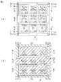
以下、本発明の車両用前照灯の第1の実施形態について説明する。図1は第1の実施形態の車両用前照灯100等を示した図である。詳細には、図1(A)は第1の実施形態の車両用前照灯100の概略的な正面図、図1(B)は図1(A)のA−A線に沿った概略的な水平断面図である。図1(C)は図1(A)に示すLEDパッケージ10のLED素子1−1,1−2,1−3,1−4の発光面1−1a1,1−2a1,1−3a1,1−4a1、シェード12のエッジ部分12a等の拡大図である。図2はケーシング4が取り付けられる前の状態におけるLEDパッケージ10の支持基板2等を示した図である。詳細には、図2(A)は支持基板2に対してLED素子1−1,1−2,1−3,1−4がフリップチップ実装された状態におけるLED素子1−1,1−2,1−3,1−4および支持基板2を第1の実施形態の車両用前照灯100の照射方向の前側(図1(B)の下側)から見た図である。図2(B)は図2(A)のB−B線に沿った概略的な断面図である。図2(C)はLED素子1−1,1−2,1−3,1−4がフリップチップ実装される前の状態における支持基板2を第1の実施形態の車両用前照灯100の照射方向の前側(図1(B)の下側)から見た図である。図2(D)は第1の実施形態の車両用前照灯100の変形例の支持基板2を示した図である。
A vehicle headlamp according to a first embodiment of the present invention will be described below. FIG. 1 is a diagram showing a vehicle headlamp 100 and the like according to the first embodiment. Specifically, FIG. 1 (A) is a schematic front view of the vehicle headlamp 100 of the first embodiment, and FIG. 1 (B) is a schematic view taken along line AA of FIG. 1 (A). FIG. 1C shows the light emitting surfaces 1-1a1, 1-2a1, 1-3a1, 1 of the LED elements 1-1, 1-2, 1-3, 1-4 of the LED package 10 shown in FIG. -4a1, an enlarged view of the edge portion 12a of the shade 12, and the like. FIG. 2 is a view showing the support substrate 2 and the like of the LED package 10 before the casing 4 is attached. Specifically, FIG. 2A shows the LED elements 1-1, 1-2 in a state where the LED elements 1-1, 1-2, 1-3, 1-4 are flip-chip mounted on the support substrate 2. , 1-3, 1-4 and the support substrate 2 are viewed from the front side (lower side of FIG. 1B) of the irradiation direction of the vehicle headlamp 100 of the first embodiment. FIG. 2B is a schematic cross-sectional view along the line BB in FIG. FIG. 2 (C) shows the support substrate 2 in a state before the LED elements 1-1, 1-2, 1-3, and 1-4 are flip-chip mounted on the vehicle headlamp 100 of the first embodiment. It is the figure seen from the front side (lower side of FIG. 1 (B)) of an irradiation direction. FIG. 2D is a view showing a support substrate 2 of a modified example of the vehicle headlamp 100 according to the first embodiment.
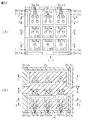
図3は図1(C)に示すLED素子1−1およびシェード12のエッジ部分12aの拡大図などである。詳細には、図3(A)は図1(C)に示すLED素子1−1およびシェード12のエッジ部分12aの拡大図である。図3(B)は図3(A)に示すLED素子1−1を裏側(第1の実施形態の車両用前照灯100の照射方向の後側(図1(B)の上側))から見た図である。図4はLED素子1−1の概略的な断面図である。詳細には、図4(A)は図3(A)のC−C線に沿った概略的な断面図、図4(B)は図3(A)のD−D線に沿った概略的な断面図、図4(C)は図3(A)のE−E線に沿った概略的な断面図である。
3 is an enlarged view of the LED element 1-1 and the edge portion 12a of the shade 12 shown in FIG. Specifically, FIG. 3A is an enlarged view of the LED element 1-1 and the edge portion 12a of the shade 12 shown in FIG. 3B shows the LED element 1-1 shown in FIG. 3A from the back side (the rear side in the irradiation direction of the vehicle headlamp 100 of the first embodiment (the upper side in FIG. 1B)). FIG. FIG. 4 is a schematic cross-sectional view of the LED element 1-1. Specifically, FIG. 4A is a schematic cross-sectional view taken along line CC in FIG. 3A, and FIG. 4B is a schematic view taken along line DD in FIG. FIG. 4C is a schematic cross-sectional view taken along the line EE of FIG.
図5および図6はLED素子1−1のp側電極1−1g1,1−1g2,1−1g3,1−1g4,1−1g5,1−1g6,1−1g7,1−1g8,1−1g9にバンプ3p1a,3p2a,3p3a,3p4a,3p5a,3p6a,3p7a,3p8a,3p9aが形成され、n側パッド電極1−1eにバンプ3n1aが形成された状態、および、支持基板2のp側配線層2aにバンプ3p1b,3p2b,3p3b,3p4b,3p5b,3p6b,3p7b,3p8b,3p9bが形成され、n側配線層2bにバンプ3n1bが形成された状態を示した図である。詳細には、図5(A)はLED素子1−1のp側電極1−1g1,1−1g2,1−1g3,1−1g4,1−1g5,1−1g6,1−1g7,1−1g8,1−1g9にバンプ3p1a,3p2a,3p3a,3p4a,3p5a,3p6a,3p7a,3p8a,3p9aが形成され、n側パッド電極1−1eにバンプ3n1aが形成された状態を第1の実施形態の車両用前照灯100の照射方向の後側(図1(B)の上側)から見た図である。図5(B)は支持基板2のp側配線層2aにバンプ3p1b,3p2b,3p3b,3p4b,3p5b,3p6b,3p7b,3p8b,3p9bが形成され、n側配線層2bにバンプ3n1bが形成された状態を第1の実施形態の車両用前照灯100の照射方向の前側(図1(B)の下側)から見た図である。図6(A)は図5(A)および図5(B)のF−F線に沿った概略的な断面図、図6(B)は図5(A)および図5(B)のG−G線に沿った概略的な断面図、図6(C)は図5(A)および図5(B)のH−H線に沿った概略的な断面図である。
5 and 6 show the p-side electrodes 1-1g1, 1-1g2, 1-1g3, 1-1g4, 1-1g5, 1-1g6, 1-1g7, 1-1g8, 1-1g9 of the LED element 1-1. The bumps 3p1a, 3p2a, 3p3a, 3p4a, 3p5a, 3p6a, 3p7a, 3p8a, 3p9a are formed, the bumps 3n1a are formed on the n-side pad electrode 1-1e, and the p-side wiring layer 2a of the support substrate 2 Are bumps 3p1b, 3p2b, 3p3b, 3p4b, 3p5b, 3p6b, 3p7b, 3p8b, 3p9b, and a state in which the bump 3n1b is formed on the n-side wiring layer 2b. Specifically, FIG. 5A shows the p-side electrodes 1-1g1, 1-1g2, 1-1g3, 1-1g4, 1-1g5, 1-1g6, 1-1g7, 1-1g8 of the LED element 1-1. , 1-1g9, bumps 3p1a, 3p2a, 3p3a, 3p4a, 3p5a, 3p6a, 3p7a, 3p8a, 3p9a are formed, and the bump 3n1a is formed on the n-side pad electrode 1-1e according to the vehicle of the first embodiment. It is the figure seen from the back side (upper side of FIG. 1 (B)) of the irradiation direction of the headlight 100 for an object. In FIG. 5B, bumps 3p1b, 3p2b, 3p3b, 3p4b, 3p5b, 3p6b, 3p7b, 3p8b, 3p9b are formed on the p-side wiring layer 2a of the support substrate 2, and bumps 3n1b are formed on the n-side wiring layer 2b. It is the figure which looked at the state from the front side (lower side of Drawing 1 (B)) of the irradiation direction of vehicular headlamp 100 of a 1st embodiment. 6A is a schematic cross-sectional view taken along line FF in FIGS. 5A and 5B, and FIG. 6B is a cross-sectional view taken along line G in FIGS. 5A and 5B. FIG. 6C is a schematic cross-sectional view taken along the line H-H in FIGS. 5A and 5B.
図7はLED素子1−1のp側電極1−1g1,1−1g2,1−1g3,1−1g4,1−1g5,1−1g6,1−1g7,1−1g8,1−1g9に形成されたバンプ3p1a,3p2a,3p3a,3p4a,3p5a,3p6a,3p7a,3p8a,3p9aと、支持基板2のp側配線層2aに形成されたバンプ3p1b,3p2b,3p3b,3p4b,3p5b,3p6b,3p7b,3p8b,3p9bとが接合された状態を示した図である。詳細には、図7(A)は図5(A)および図5(B)のF−F線に沿った断面内におけるLED素子1−1のバンプ3p1a,3p2a,3p3aと支持基板2のバンプ3p1b,3p2b,3p3bとが接合された状態を示した図である。図7(B)は図5(A)および図5(B)のG−G線に沿った断面内におけるLED素子1−1のバンプ3p4a,3p5a,3p6aと支持基板2のバンプ3p4b,3p5b,3p6bとが接合された状態を示した図である。図7(C)は図5(A)および図5(B)のH−H線に沿った断面内におけるLED素子1−1のバンプ3p7a,3p8a,3p9aと支持基板2のバンプ3p7b,3p8b,3p9bとが接合された状態を示した図である。
7 is formed on the p-side electrodes 1-1g1, 1-1g2, 1-1g3, 1-1g4, 1-1g5, 1-1g6, 1-1g7, 1-1g8, 1-1g9 of the LED element 1-1. Bumps 3p1a, 3p2a, 3p3a, 3p4a, 3p5a, 3p6a, 3p7a, 3p8a, 3p9a, and bumps 3p1b, 3p2b, 3p3b, 3p4b, 3p5b, 3p6b, 3p7b, 3p7b, 3p7b, 3p7b , 3p9b are joined to each other. Specifically, FIG. 7A shows the bumps 3p1a, 3p2a, 3p3a of the LED element 1-1 and the bumps of the support substrate 2 in the cross section taken along the line FF in FIGS. 5A and 5B. It is the figure which showed the state by which 3p1b, 3p2b, and 3p3b were joined. 7B shows the bumps 3p4a, 3p5a, 3p6a of the LED element 1-1 and the bumps 3p4b, 3p5b of the support substrate 2 in the cross section taken along the line GG of FIGS. 5A and 5B. It is the figure which showed the state in which 3p6b was joined. FIG. 7C shows bumps 3p7a, 3p8a, 3p9a of the LED element 1-1 and bumps 3p7b, 3p8b of the support substrate 2 in the cross section taken along the line HH of FIGS. 5A and 5B. It is the figure which showed the state in which 3p9b was joined.
図8は第1の実施形態の車両用前照灯100のLEDパッケージ10のLED素子1−1のLED素子基板1−1aの発光面1−1a1内の位置(図8のグラフの横軸)と輝度(図8のグラフの縦軸)との関係などを示した図である。図9は第1の実施形態の車両用前照灯100によって形成されるカットラインP1Cを有する配光パターンP1を示した図である。
FIG. 8 shows the position in the light emitting surface 1-1a1 of the LED element substrate 1-1a of the LED element 1-1 of the LED package 10 of the vehicle headlamp 100 of the first embodiment (horizontal axis of the graph of FIG. 8). It is the figure which showed the relationship etc. with a brightness | luminance (vertical axis | shaft of the graph of FIG. 8). FIG. 9 is a view showing a light distribution pattern P1 having a cut line P1C formed by the vehicle headlamp 100 according to the first embodiment.
第1の実施形態の車両用前照灯100では、投影レンズ11(図1(A)および図1(B)参照)の焦点11a(図1(B)参照)上またはその近傍にLEDパッケージ10(図1(A)、図1(B)および図1(C)参照)と、シェード12(図1(A)、図1(B)、図1(C)および図3(A)参照)とが配置されている。詳細には、第1の実施形態の車両用前照灯100では、図1(A)および図1(B)に示すように、例えば、LEDパッケージ10がヒートシンク14に搭載されている。また、ヒートシンク14と投影レンズ11とが、レンズホルダ13を介して接続されている。更に、LEDパッケージ10と投影レンズ11とシェード12とレンズホルダ13とヒートシンク14とによって構成されるランプユニットが、ハウジング100aとカバーレンズ100bとによって画定される灯室100c内に収容されている。また、LEDパッケージ10と投影レンズ11とシェード12とレンズホルダ13とヒートシンク14とによって構成されるランプユニットが、エイミングスクリュー100dを介してハウジング100aに接続されている。
In the vehicle headlamp 100 of the first embodiment, the LED package 10 is on or near the focal point 11a (see FIG. 1B) of the projection lens 11 (see FIGS. 1A and 1B). (See FIGS. 1A, 1B, and 1C) and shade 12 (see FIGS. 1A, 1B, 1C, and 3A) And are arranged. Specifically, in the vehicle headlamp 100 of the first embodiment, for example, the LED package 10 is mounted on the heat sink 14 as shown in FIGS. 1 (A) and 1 (B). Further, the heat sink 14 and the projection lens 11 are connected via the lens holder 13. Further, a lamp unit including the LED package 10, the projection lens 11, the shade 12, the lens holder 13, and the heat sink 14 is accommodated in a lamp chamber 100c defined by the housing 100a and the cover lens 100b. A lamp unit including the LED package 10, the projection lens 11, the shade 12, the lens holder 13, and the heat sink 14 is connected to the housing 100a via an aiming screw 100d.
更に、第1の実施形態の車両用前照灯100では、図1(C)に示すように、例えば4個のLED素子1−1,1−2,1−3,1−4と、支持基板2と、貫通穴4aを有するケーシング4とが、LEDパッケージ10に設けられている。詳細には、第1の実施形態の車両用前照灯100では、LED素子1−1と、LED素子1−2と、LED素子1−3と、LED素子1−4とが同様に構成されている。また、第1の実施形態の車両用前照灯100では、例えば、波長が460nmの青色を発光するLED素子1−1,1−2,1−3,1−4が用いられ、ケーシング4の貫通穴4a内に例えば黄色味を帯びた例えばYAG系の蛍光体が充填されている。そのため、第1の実施形態の車両用前照灯100では、例えば、LED素子1−1,1−2,1−3,1−4が発光すると、ケーシング4の貫通穴4a内の蛍光体が励起される。その結果、発光色が混色されて、白色を帯びた光がLEDパッケージ10から照射される。
Furthermore, in the vehicle headlamp 100 of the first embodiment, as shown in FIG. 1C, for example, four LED elements 1-1, 1-2, 1-3, 1-4, and a support A substrate 2 and a casing 4 having a through hole 4 a are provided in the LED package 10. Specifically, in the vehicle headlamp 100 according to the first embodiment, the LED element 1-1, the LED element 1-2, the LED element 1-3, and the LED element 1-4 are configured in the same manner. ing. In the vehicle headlamp 100 according to the first embodiment, for example, LED elements 1-1, 1-2, 1-3, and 1-4 that emit blue light having a wavelength of 460 nm are used. The through-hole 4a is filled with, for example, a yellowish phosphor such as YAG. Therefore, in the vehicle headlamp 100 of the first embodiment, for example, when the LED elements 1-1, 1-2, 1-3, and 1-4 emit light, the phosphor in the through hole 4a of the casing 4 is changed. Excited. As a result, the light emission colors are mixed, and white light is emitted from the LED package 10.
第1の実施形態の車両用前照灯100では、4個のLED素子1−1,1−2,1−3,1−4がLEDパッケージ10に設けられているが、第1の実施形態の車両用前照灯100の変形例では、代わりに、4個以外の任意の数のLED素子をLEDパッケージ10に設けることも可能である。また、第1の実施形態の車両用前照灯100では、例えば1mm□のLED素子1−1,1−2,1−3,1−4が用いられているが、第1の実施形態の車両用前照灯100の変形例では、代わりに、第1の実施形態の車両用前照灯100のLED素子1−1,1−2,1−3,1−4とはサイズが異なるLED素子を用いることも可能である。更に、第1の実施形態の車両用前照灯100では、LED素子1−1,1−2,1−3,1−4の相互の間隔が例えば100μmに設定されているが、第1の実施形態の車両用前照灯100の変形例では、代わりに、LED素子1−1,1−2,1−3,1−4の相互の間隔を100μm以外の任意の値に設定することも可能である。
In the vehicle headlamp 100 of the first embodiment, the four LED elements 1-1, 1-2, 1-3, and 1-4 are provided in the LED package 10, but the first embodiment In the modified example of the vehicle headlamp 100, any number of LED elements other than four can be provided in the LED package 10 instead. Further, in the vehicle headlamp 100 of the first embodiment, for example, 1 mm square LED elements 1-1, 1-2, 1-3, and 1-4 are used. In the modified example of the vehicle headlamp 100, instead, the LED is different in size from the LED elements 1-1, 1-2, 1-3, and 1-4 of the vehicle headlamp 100 of the first embodiment. It is also possible to use elements. Furthermore, in the vehicle headlamp 100 of the first embodiment, the mutual distance between the LED elements 1-1, 1-2, 1-3, and 1-4 is set to 100 μm, for example. In the modified example of the vehicle headlamp 100 of the embodiment, instead, the mutual distance between the LED elements 1-1, 1-2, 1-3, and 1-4 may be set to an arbitrary value other than 100 μm. Is possible.
また、第1の実施形態の車両用前照灯100では、図2(C)に示すように、例えば、p側配線層2aと、n側配線層2bとが、例えばSi、AlN、SiC、AlO2などによって形成された支持基板2に設けられている。更に、第1の実施形態の車両用前照灯100では、図4に示すように、例えば、LED素子基板1−1aと、n型半導体層1−1bと、発光層1−1c1,1−1c2,1−1c3,1−1c4,1−1c5,1−1c6,1−1c7,1−1c8,1−1c9とが、LED素子1−1に設けられている。詳細には、例えば、図4(A)に示すように、発光層1−1c7,1−1c8,1−1c9に隣接してp型半導体層1−1d7,1−1d8,1−1d9が形成され、図4(B)に示すように、発光層1−1c4,1−1c5,1−1c6に隣接してp型半導体層1−1d4,1−1d5,1−1d6が形成され、図4(C)に示すように、発光層1−1c1,1−1c2,1−1c3に隣接してp型半導体層1−1d1,1−1d2,1−1d3が形成されている。更に、例えば、図4(A)に示すように、p型半導体層1−1d7,1−1d8,1−1d9に隣接してp側電極1−1g7,1−1g8,1−1g9が形成され、図4(B)に示すように、p型半導体層1−1d4,1−1d5,1−1d6に隣接してp側電極1−1g4,1−1g5,1−1g6が形成され、図4(C)に示すように、p型半導体層1−1d1,1−1d2,1−1d3に隣接してp側電極1−1g1,1−1g2,1−1g3が形成されている。つまり、第1の実施形態の車両用前照灯100では、LED素子1−1の発光層1−1c1,1−1c2,1−1c3,1−1c4,1−1c5,1−1c6,1−1c7,1−1c8,1−1c9が発光すると、LED素子基板1−1aの表面(図4の上側の表面)が発光面1−1a1として機能する。
Further, in the vehicle headlamp 100 of the first embodiment, as shown in FIG. 2C, for example, the p-side wiring layer 2a and the n-side wiring layer 2b are made of, for example, Si, AlN, SiC, A support substrate 2 made of AlO 2 or the like is provided. Furthermore, in the vehicle headlamp 100 of the first embodiment, as shown in FIG. 4, for example, an LED element substrate 1-1a, an n-type semiconductor layer 1-1b, and a light emitting layer 1-1c1, 1- 1c2, 1-1c3, 1-1c4, 1-1c5, 1-1c6, 1-1c7, 1-1c8, 1-1c9 are provided in the LED element 1-1. Specifically, for example, as shown in FIG. 4A, p-type semiconductor layers 1-1d7, 1-1d8, 1-1d9 are formed adjacent to the light emitting layers 1-1c7, 1-1c8, 1-1c9. As shown in FIG. 4B, p-type semiconductor layers 1-1d4, 1-1d5, 1-1d6 are formed adjacent to the light emitting layers 1-1c4, 1-1c5, 1-1c6. As shown in (C), p-type semiconductor layers 1-1d1, 1-1d2, 1-1d3 are formed adjacent to the light emitting layers 1-1c1, 1-1c2, 1-1c3. Further, for example, as shown in FIG. 4A, p-side electrodes 1-1g7, 1-1g8, 1-1g9 are formed adjacent to the p-type semiconductor layers 1-1d7, 1-1d8, 1-1d9. As shown in FIG. 4B, p-side electrodes 1-1g4, 1-1g5, 1-1g6 are formed adjacent to the p-type semiconductor layers 1-1d4, 1-1d5, 1-1d6. As shown in (C), p-side electrodes 1-1g1, 1-1g2, and 1-1g3 are formed adjacent to the p-type semiconductor layers 1-1d1, 1-1d2, and 1-1d3. That is, in the vehicle headlamp 100 of the first embodiment, the light emitting layers 1-1c1, 1-1c2, 1-1c3, 1-1c4, 1-1c5, 1-1c6, 1-c1, 1- of the LED element 1-1. When 1c7, 1-1c8, 1-1c9 emits light, the surface of the LED element substrate 1-1a (the upper surface in FIG. 4) functions as the light emitting surface 1-1a1.
第1の実施形態の車両用前照灯100では、図2(C)に示すように、例えば、p側配線層2aと、n側配線層2bとが、例えばSi、AlN、SiC、AlO2などによって形成された支持基板2に設けられているが、第1の実施形態の車両用前照灯100の変形例では、代わりに、図2(D)に示すように、例えば、p側配線層2aと、n側配線層2bとを、例えばSi、AlN、SiC、AlO2などによって形成された支持基板2に設けることも可能である。
In the vehicle headlamp 100 of the first embodiment, as shown in FIG. 2C, for example, the p-side wiring layer 2a and the n-side wiring layer 2b are made of, for example, Si, AlN, SiC, AlO 2. In the modified example of the vehicle headlamp 100 according to the first embodiment, instead, as shown in FIG. 2D, for example, p-side wiring is provided. It is also possible to provide the layer 2a and the n-side wiring layer 2b on the support substrate 2 formed of, for example, Si, AlN, SiC, AlO 2 or the like.
更に、第1の実施形態の車両用前照灯100では、図4に示すように、例えば、n側パッド電極1−1eと、n側オーミック電極1−1fとが、LED素子1−1に設けられている。詳細には、第1の実施形態の車両用前照灯100では、図3に示すように、例えば9個のp側電極1−1g1,1−1g2,1−1g3,1−1g4,1−1g5,1−1g6,1−1g7,1−1g8,1−1g9が、例えば図3の縦3列×図3の横3列に配列されている。また、例えば4個のn側パッド電極1−1eが、LED素子1−1の例えば4隅に配置されている。第1の実施形態の車両用前照灯100では、9個のp側電極1−1g1,1−1g2,1−1g3,1−1g4,1−1g5,1−1g6,1−1g7,1−1g8,1−1g9が図3の縦3列×図3の横3列に配列されているが、第1の実施形態の車両用前照灯100の変形例では、代わりに、9個より多い任意の数のp側電極をLED素子1−1に設け、図3の縦4列以上になるように複数のp側電極を配列することにより、LED素子1−1の発光面1−1a1の輝度勾配を緩やかにすることも可能である。また、第1の実施形態の車両用前照灯100では、n側パッド電極1−1eがLED素子1−1の4隅に配置されているが、第1の実施形態の車両用前照灯100の変形例では、代わりに、n側パッド電極をLED素子1−1の4隅以外の任意の位置に配置することも可能である。
Furthermore, in the vehicle headlamp 100 according to the first embodiment, as illustrated in FIG. 4, for example, an n-side pad electrode 1-1 e and an n-side ohmic electrode 1-1 f are formed on the LED element 1-1. Is provided. Specifically, in the vehicle headlamp 100 according to the first embodiment, as shown in FIG. 3, for example, nine p-side electrodes 1-1g1, 1-1g2, 1-1g3, 1-1g4, 1- 1g5, 1-1g6, 1-1g7, 1-1g8, and 1-1g9 are arranged in, for example, three vertical columns in FIG. 3 × three horizontal rows in FIG. Further, for example, four n-side pad electrodes 1-1e are arranged at, for example, four corners of the LED element 1-1. In the vehicle headlamp 100 according to the first embodiment, nine p-side electrodes 1-1g1, 1-1g2, 1-1g3, 1-1g4, 1-1g5, 1-1g6, 1-1g7, 1- 1g8 and 1-1g9 are arranged in 3 vertical rows of FIG. 3 × 3 horizontal rows of FIG. 3, but in the modified example of the vehicle headlamp 100 of the first embodiment, there are more than 9 instead. An arbitrary number of p-side electrodes are provided on the LED element 1-1, and a plurality of p-side electrodes are arranged so as to be four or more columns in FIG. It is also possible to make the luminance gradient gentle. Further, in the vehicle headlamp 100 of the first embodiment, the n-side pad electrode 1-1e is arranged at the four corners of the LED element 1-1, but the vehicle headlamp of the first embodiment is used. In the modification of 100, it is also possible to arrange the n-side pad electrode at an arbitrary position other than the four corners of the LED element 1-1 instead.
また、第1の実施形態の車両用前照灯100では、図3および図4に示すLED素子1−1を図2(C)に示す支持基板2に実装するために、図5(A)および図6に示すように、LED素子1−1のp側電極1−1g1に、例えば金バンプなどのような3個のバンプ3p1aが形成され、LED素子1−1のp側電極1−1g2に、例えば金バンプなどのような3個のバンプ3p2aが形成され、LED素子1−1のp側電極1−1g3に、例えば金バンプなどのような3個のバンプ3p3aが形成され、LED素子1−1のp側電極1−1g4に、例えば金バンプなどのような2個のバンプ3p4aが形成され、LED素子1−1のp側電極1−1g5に、例えば金バンプなどのような2個のバンプ3p5aが形成され、LED素子1−1のp側電極1−1g6に、例えば金バンプなどのような2個のバンプ3p6aが形成され、LED素子1−1のp側電極1−1g7に、例えば金バンプなどのような1個のバンプ3p7aが形成され、LED素子1−1のp側電極1−1g8に、例えば金バンプなどのような1個のバンプ3p8aが形成され、LED素子1−1のp側電極1−1g9に、例えば金バンプなどのような1個のバンプ3p9aが形成されている。また、図5(A)に示すように、LED素子1−1のn側パッド電極1−1eに、例えば金バンプなどのようなバンプ3n1aが形成されている。
Further, in the vehicle headlamp 100 of the first embodiment, in order to mount the LED element 1-1 shown in FIGS. 3 and 4 on the support substrate 2 shown in FIG. 2C, FIG. As shown in FIG. 6, three bumps 3p1a such as gold bumps are formed on the p-side electrode 1-1g1 of the LED element 1-1, and the p-side electrode 1-1g2 of the LED element 1-1 is formed. Three bumps 3p2a such as gold bumps are formed, and three bumps 3p3a such as gold bumps are formed on the p-side electrode 1-1g3 of the LED element 1-1. Two bumps 3p4a such as gold bumps are formed on the p-side electrode 1-1g4 of 1-1, and two bumps 3p4a such as gold bumps are formed on the p-side electrode 1-1g5 of the LED element 1-1. Bumps 3p5a are formed, and LED element 1- Two bumps 3p6a such as gold bumps are formed on the p-side electrode 1-1g6, and one bump such as gold bumps is formed on the p-side electrode 1-1g7 of the LED element 1-1. 3p7a is formed, one bump 3p8a such as a gold bump is formed on the p-side electrode 1-1g8 of the LED element 1-1, and the p-side electrode 1-1g9 of the LED element 1-1 is One bump 3p9a such as a gold bump is formed. Further, as shown in FIG. 5A, a bump 3n1a such as a gold bump is formed on the n-side pad electrode 1-1e of the LED element 1-1.
更に、第1の実施形態の車両用前照灯100では、図3および図4に示すLED素子1−1を図2(C)に示す支持基板2に実装するために、図5(B)および図6に示すように、支持基板2のp側配線層2aに、例えば金バンプなどのような3個のバンプ3p1bが形成され、例えば金バンプなどのような3個のバンプ3p2bが形成され、例えば金バンプなどのような3個のバンプ3p3bが形成され、例えば金バンプなどのような2個のバンプ3p4bが形成され、例えば金バンプなどのような2個のバンプ3p5bが形成され、例えば金バンプなどのような2個のバンプ3p6bが形成され、例えば金バンプなどのような1個のバンプ3p7bが形成され、例えば金バンプなどのような1個のバンプ3p8bが形成され、例えば金バンプなどのような1個のバンプ3p9bが形成されている。更に、図5(B)に示すように、支持基板2のn側配線層2bに、例えば金バンプなどのようなバンプ3n1bが形成されている。
Furthermore, in the vehicle headlamp 100 of the first embodiment, in order to mount the LED element 1-1 shown in FIGS. 3 and 4 on the support substrate 2 shown in FIG. 2C, FIG. As shown in FIG. 6, three bumps 3 p 1 b such as gold bumps are formed on the p-side wiring layer 2 a of the support substrate 2, and three bumps 3 p 2 b such as gold bumps are formed. For example, three bumps 3p3b such as gold bumps are formed, two bumps 3p4b such as gold bumps are formed, and two bumps 3p5b such as gold bumps are formed. Two bumps 3p6b such as gold bumps are formed, one bump 3p7b such as a gold bump is formed, and one bump 3p8b such as a gold bump is formed. One bump 3p9b like flop is formed. Further, as shown in FIG. 5B, bumps 3n1b such as gold bumps are formed on the n-side wiring layer 2b of the support substrate 2, for example.
更に、第1の実施形態の車両用前照灯100では、図7に示すように、図3および図4に示すLED素子1−1が、図2(C)に示す支持基板2に対してフリップチップ実装されている。詳細には、第1の実施形態の車両用前照灯100では、図5および図7に示すように、例えば超音波振動によって、LED素子1−1の3個のバンプ3p1aと支持基板2の3個のバンプ3p1bとが融着・接合され(図7(A)参照)、LED素子1−1の3個のバンプ3p2aと支持基板2の3個のバンプ3p2bとが融着・接合され(図7(A)参照)、LED素子1−1の3個のバンプ3p3aと支持基板2の3個のバンプ3p3bとが融着・接合され(図7(A)参照)、LED素子1−1の2個のバンプ3p4aと支持基板2の2個のバンプ3p4bとが融着・接合され(図7(B)参照)、LED素子1−1の2個のバンプ3p5aと支持基板2の2個のバンプ3p5bとが融着・接合され(図7(B)参照)、LED素子1−1の2個のバンプ3p6aと支持基板2の2個のバンプ3p6bとが融着・接合され(図7(B)参照)、LED素子1−1の1個のバンプ3p7aと支持基板2の1個のバンプ3p7bとが融着・接合され(図7(C)参照)、LED素子1−1の1個のバンプ3p8aと支持基板2の1個のバンプ3p8bとが融着・接合され(図7(C)参照)、LED素子1−1の1個のバンプ3p9aと支持基板2の1個のバンプ3p9bとが融着・接合され(図7(C)参照)、LED素子1−1の4個のバンプ3n1a(図5(A)参照)と支持基板2の4個のバンプ3n1b(図5(B)参照)とが融着・接合されている。
Furthermore, in the vehicle headlamp 100 of the first embodiment, as shown in FIG. 7, the LED element 1-1 shown in FIGS. 3 and 4 is in contrast to the support substrate 2 shown in FIG. Flip chip mounting. Specifically, in the vehicle headlamp 100 of the first embodiment, as shown in FIGS. 5 and 7, the three bumps 3 p 1 a of the LED element 1-1 and the support substrate 2 are formed by, for example, ultrasonic vibration. Three bumps 3p1b are fused and bonded (see FIG. 7A), and three bumps 3p2a of the LED element 1-1 and three bumps 3p2b of the support substrate 2 are fused and bonded ( The three bumps 3p3a of the LED element 1-1 and the three bumps 3p3b of the support substrate 2 are fused and joined (see FIG. 7A), and the LED element 1-1. The two bumps 3p4a and the two bumps 3p4b of the support substrate 2 are fused and joined (see FIG. 7B), and the two bumps 3p5a of the LED element 1-1 and the support substrate 2 are two. The bump 3p5b is fused and joined (see FIG. 7B), and the LED element 1 The two bumps 3p6a of 1 and the two bumps 3p6b of the support substrate 2 are fused and joined (see FIG. 7B), and one bump 3p7a of the LED element 1-1 and 1 of the support substrate 2 The bumps 3p7b are fused and joined (see FIG. 7C), and one bump 3p8a of the LED element 1-1 and one bump 3p8b of the support substrate 2 are fused and joined (see FIG. 7). 7C), one bump 3p9a of the LED element 1-1 and one bump 3p9b of the support substrate 2 are fused and joined (see FIG. 7C), and the LED element 1-1 Four bumps 3n1a (see FIG. 5A) and four bumps 3n1b (see FIG. 5B) of the support substrate 2 are fused and joined.
その結果、第1の実施形態の車両用前照灯100では、図7に示すように、支持基板2からバンプ3p1b,3p2b,3p3b,3p4b,3p5b,3p6b,3p7b,3p8b,3p9bおよびバンプ3p1a,3p2a,3p3a,3p4a,3p5a,3p6a,3p7a,3p8a,3p9aを介してLED素子1−1のp側電極1−1g1,1−1g2,1−1g3,1−1g4,1−1g5,1−1g6,1−1g7,1−1g8,1−1g9(図5(A)参照)に電流が流れる。また、第1の実施形態の車両用前照灯100では、LED素子1−1(図5(A)参照)のn側パッド電極1−1e(図5(A)参照)からバンプ3n1a(図5(A)参照)およびバンプ3n1b(図5(B)参照)を介して支持基板2(図5(B)参照)に電流が流れる。
As a result, in the vehicle headlamp 100 of the first embodiment, as shown in FIG. 7, the bumps 3p1b, 3p2b, 3p3b, 3p4b, 3p5b, 3p6b, 3p7b, 3p8b, 3p9b and the bumps 3p1a, 3p2a, 3p3a, 3p4a, 3p5a, 3p6a, 3p7a, 3p8a, 3p9a through the p-side electrodes 1-1g1, 1-1g2, 1-1g3, 1-1g4, 1-1g5, 1-1g6 of the LED element 1-1 , 1-1g7, 1-1g8, 1-1g9 (see FIG. 5A). Further, in the vehicle headlamp 100 of the first embodiment, the bump 3n1a (see FIG. 5) from the n-side pad electrode 1-1e (see FIG. 5 (A)) of the LED element 1-1 (see FIG. 5 (A)). 5A) and the bump 3n1b (see FIG. 5B), a current flows through the support substrate 2 (see FIG. 5B).
同様に、第1の実施形態の車両用前照灯100では、図2(A)および図2(B)に示すように、LED素子1−2,1−3,1−4が支持基板2に対してフリップチップ実装されている。
Similarly, in the vehicle headlamp 100 of the first embodiment, as shown in FIGS. 2 (A) and 2 (B), the LED elements 1-2, 1-3, and 1-4 are supported by the support substrate 2. In contrast, it is flip-chip mounted.
更に、第1の実施形態の車両用前照灯100では、LEDパッケージ10(図1参照)のLED素子1−1,1−2,1−3,1−4(図1(C)参照)の発光面1−1a1,1−2a1,1−3a1,1−4a1(図1(C)参照)およびシェード12(図1参照)のエッジ部分12a(図1参照)を投影レンズ11(図1(A)および図1(B)参照)によって投影することにより、シェード12のエッジ部分12aに対応するカットラインP1C(図9参照)を有する配光パターンP1(図9参照)が形成される。
Furthermore, in the vehicle headlamp 100 of the first embodiment, the LED elements 1-1, 1-2, 1-3, 1-4 of the LED package 10 (see FIG. 1) (see FIG. 1C). The light emitting surfaces 1-1a1, 1-2a1, 1-3a1, 1-4a1 (see FIG. 1C) and the edge portion 12a (see FIG. 1) of the shade 12 (see FIG. 1) are projected onto the projection lens 11 (see FIG. 1). By projecting according to (A) and FIG. 1 (B)), a light distribution pattern P1 (see FIG. 9) having a cut line P1C (see FIG. 9) corresponding to the edge portion 12a of the shade 12 is formed.
ところで、仮に、LEDパッケージ10(図1参照)のLED素子1−2,1−3,1−4(図1(C)参照)の発光面1−1a1,1−2a1,1−3a1,1−4a1(図1(C)参照)全体が均一に発光するようにLEDパッケージ10が構成されている場合には、カットラインP1C(図9参照)の近傍の部分(図9中のF−F線上の部分)の輝度とカットラインP1C(図9参照)から離れている部分(図9中のG−G線上の部分、図9中のH−H線上の部分)の輝度とがほぼ等しい配光パターンP1(図9参照)が形成されてしまう。
By the way, temporarily, the light emitting surfaces 1-1a1, 1-2a1, 1-3a1, 1 of the LED elements 1-2, 1-3, 1-4 (see FIG. 1C) of the LED package 10 (see FIG. 1). -4a1 (see FIG. 1C), the LED package 10 is configured to emit light uniformly, and a portion in the vicinity of the cut line P1C (see FIG. 9) (F-F in FIG. 9). The luminance of the portion on the line) and the luminance of the portion (the portion on the GG line in FIG. 9 and the portion on the HH line in FIG. 9) far from the cut line P1C (see FIG. 9) The light pattern P1 (see FIG. 9) is formed.
この点に鑑み、第1の実施形態の車両用前照灯100では、図7に示すように、LED素子1−1の複数の電極1−1g1,1−1g2,1−1g3,1−1g4,1−1g5,1−1g6,1−1g7,1−1g8,1−1g9(図5(A)参照)から支持基板2の側に延びている略同一の直径を有する複数のバンプ3p1a,3p2a,3p3a,3p4a,3p5a,3p6a,3p7a,3p8a,3p9aと、支持基板2からLED素子1−1の複数の電極1−1g1,1−1g2,1−1g3,1−1g4,1−1g5,1−1g6,1−1g7,1−1g8,1−1g9の側に延びている略同一の直径を有する複数のバンプ3p1b,3p2b,3p3b,3p4b,3p5b,3p6b,3p7b,3p8b,3p9bとを接合することによってLED素子1−1の各電極1−1g1,1−1g2,1−1g3,1−1g4,1−1g5,1−1g6,1−1g7,1−1g8,1−1g9と支持基板2とが電気的および熱的に接続されている。
In view of this point, in the vehicle headlamp 100 according to the first embodiment, as shown in FIG. 7, the plurality of electrodes 1-1g1, 1-1g2, 1-1g3, 1-1g4 of the LED element 1-1. 1, 1-1 g 5, 1-1 g 6, 1-1 g 7, 1-1 g 8, 1-1 g 9 (see FIG. 5A), a plurality of bumps 3 p 1 a and 3 p 2 a having substantially the same diameter extending toward the support substrate 2. , 3p3a, 3p4a, 3p5a, 3p6a, 3p7a, 3p8a, 3p9a and a plurality of electrodes 1-1g1, 1-1g2, 1-1g3, 1-1g4, 1-1g5, 1 from the support substrate 2 to the LED element 1-1 A plurality of bumps 3p1b, 3p2b, 3p3b, 3p4b, 3p5b, 3p6b, 3p7b, 3p8b, and 3p9b having substantially the same diameter extending toward -1g6, 1-1g7, 1-1g8, and 1-1g9. By combining the electrodes 1-1g1, 1-1g2, 1-1g3, 1-1g4, 1-1g5, 1-1g5, 1-1g7, 1-1g8, 1-1g9 and the supporting substrate of the LED element 1-1 2 is electrically and thermally connected.
更に、第1の実施形態の車両用前照灯100では、複数の電極1−1g1,1−1g2,1−1g3,1−1g4,1−1g5,1−1g6,1−1g7,1−1g8,1−1g9(図3および図5(A)参照)のうち、シェード12(図1(C)および図3(A)参照)のエッジ部分12a(図1(C)および図3(A)参照)から第1の距離の位置(最も近い位置)に配置された電極1−1g1,1−1g2,1−1g3(図3および図5(A)参照)から支持基板2(図5(B)参照)への伝熱量が、シェード12のエッジ部分12aから第1の距離より大きい第2の距離の位置(2番目に近い位置)に配置された電極1−1g4,1−1g5,1−1g6(図3および図5(A)参照)から支持基板2への伝熱量よりも大きくなるように、シェード12のエッジ部分12aから第1の距離の位置に配置された電極1−1g1,1−1g2,1−1g3と支持基板2とを接続する複数のバンプ3p1a,3p1b,3p2a,3p2b,3p3a,3p3b(図5、図6(A)および図7(A)参照)の配置(詳細には、バンプ3p1a,3p1b,3p2a,3p2b,3p3a,3p3bの数)と、シェード12のエッジ部分12aから第2の距離の位置(2番目に近い位置)に配置された電極1−1g4,1−1g5,1−1g6と支持基板2とを接続する複数のバンプ3p4a,3p4b,3p5a,3p5b,3p6a,3p6b(図5、図6(B)および図7(B)参照)の配置(詳細には、バンプ3p4a,3p4b,3p5a,3p5b,3p6a,3p6bの数)とが異ならされている。
Furthermore, in the vehicle headlamp 100 of the first embodiment, the plurality of electrodes 1-1g1, 1-1g2, 1-1g3, 1-1g4, 1-1g5, 1-1g6, 1-1g7, 1-1g8 , 1-1g9 (see FIGS. 3 and 5A), the edge portion 12a (see FIGS. 1C and 3A) of the shade 12 (see FIGS. 1C and 3A). (Refer to FIG. 3 and FIG. 5 (A)) to the support substrate 2 (FIG. 5 (B)). The electrodes 1-1g1, 1-1g2, 1-1g3 (refer to FIG. 3 and FIG. ) See)), the electrodes 1-1g4, 1-1g5, 1- 1 disposed at the second distance position (the second closest position) larger than the first distance from the edge portion 12a of the shade 12. 1g6 (see FIG. 3 and FIG. 5 (A)) is larger than the heat transfer amount to the support substrate 2 In addition, a plurality of bumps 3p1a, 3p1b, 3p2a, 3p2b, which connect the electrodes 1-1g1, 1-1g2, 1-1g3 and the support substrate 2 disposed at a first distance from the edge portion 12a of the shade 12; 3p3a, 3p3b (see FIG. 5, FIG. 6A and FIG. 7A) (specifically, the number of bumps 3p1a, 3p1b, 3p2a, 3p2b, 3p3a, 3p3b) and the edge portion 12a of the shade 12 A plurality of bumps 3p4a, 3p4b, 3p5a, 3p5b, 3p6a connecting the electrodes 1-1g4, 1-1g5, 1-1g6 disposed at the second distance position (the second closest position) to the support substrate 2 , 3p6b (see FIG. 5, FIG. 6B and FIG. 7B) (specifically, bumps 3p4a, 3p4b, 3p5a, 3p5b, 3p6a, 3p6) Number) and is different from the.
また、第1の実施形態の車両用前照灯100では、複数の電極1−1g1,1−1g2,1−1g3,1−1g4,1−1g5,1−1g6,1−1g7,1−1g8,1−1g9(図3および図5(A)参照)のうち、シェード12(図1(C)および図3(A)参照)のエッジ部分12a(図1(C)および図3(A)参照)から第2の距離の位置(2番目に近い位置)に配置された電極1−1g4,1−1g5,1−1g6(図3および図5(A)参照)から支持基板2(図5(B)参照)への伝熱量が、シェード12のエッジ部分12aから第2の距離より大きい第3の距離の位置(最も離れた位置)に配置された電極1−1g7,1−1g8,1−1g9(図3および図5(A)参照)から支持基板2への伝熱量よりも大きくなるように、シェード12のエッジ部分12aから第2の距離の位置に配置された電極1−1g4,1−1g5,1−1g6と支持基板2とを接続する複数のバンプ3p4a,3p4b,3p5a,3p5b,3p6a,3p6b(図5、図6(B)および図7(B)参照)の配置(詳細には、バンプ3p4a,3p4b,3p5a,3p5b,3p6a,3p6bの数)と、シェード12のエッジ部分12aから第3の距離の位置(最も離れた位置)に配置された電極1−1g7,1−1g8,1−1g9と支持基板2とを接続する複数のバンプ3p7a,3p7b,3p8a,3p8b,3p9a,3p9b(図5、図6(C)および図7(C)参照)の配置(詳細には、バンプ3p7a,3p7b,3p8a,3p8b,3p9a,3p9bの数)とが異ならされている。
Moreover, in the vehicle headlamp 100 of the first embodiment, the plurality of electrodes 1-1g1, 1-1g2, 1-1g3, 1-1g4, 1-1g5, 1-1g6, 1-1g7, 1-1g8 , 1-1g9 (see FIGS. 3 and 5A), the edge portion 12a (see FIGS. 1C and 3A) of the shade 12 (see FIGS. 1C and 3A). To the support substrate 2 (FIG. 5) from the electrodes 1-1g4, 1-1g5, 1-1g6 (see FIG. 3 and FIG. 5 (A)) disposed at the second distance (the position closest to the second). The electrodes 1-1g7, 1-1g8, 1 disposed at a third distance position (the farthest position) larger than the second distance from the edge portion 12a of the shade 12 is the amount of heat transfer to (see (B)). −1g9 (see FIG. 3 and FIG. 5 (A)) to be larger than the heat transfer amount to the support substrate 2 In other words, a plurality of bumps 3p4a, 3p4b, 3p5a, 3p5b, which connect the electrodes 1-1g4, 1-1g5, 1-1g6 disposed at the second distance from the edge portion 12a of the shade 12 and the support substrate 2, 3p6a, 3p6b (see FIG. 5, FIG. 6B and FIG. 7B) (specifically, the number of bumps 3p4a, 3p4b, 3p5a, 3p5b, 3p6a, 3p6b) and the edge portion 12a of the shade 12 A plurality of bumps 3p7a, 3p7b, 3p8a, 3p8b, 3p9a, which connect the electrodes 1-1g7, 1-1g8, 1-1g9 arranged at the third distance position (the farthest position) and the support substrate 2. 3p9b (see FIG. 5, FIG. 6C and FIG. 7C) (specifically, bumps 3p7a, 3p7b, 3p8a, 3p8b, 3p9a, 3p9) Number) and is different from the.
そのため、第1の実施形態の車両用前照灯100によれば、LEDパッケージ10(図1(C)参照)の発光面1−1a1(図1(C)参照)のうち、シェード12(図1(C)および図3(A)参照)のエッジ部分12a(図1(C)および図3(A)参照)から第1の距離の位置(最も近い位置)に配置された電極1−1g1,1−1g2,1−1g3(図3(A)参照)の背面に位置する部分の輝度を、シェード12のエッジ部分12aから第1の距離より大きい第2の距離の位置(2番目に近い位置)に配置された電極1−1g4,1−1g5,1−1g6(図3(A)参照)の背面に位置する部分の輝度よりも高くすることができる。
Therefore, according to the vehicle headlamp 100 of the first embodiment, the shade 12 (see FIG. 1C) of the light emitting surface 1-1a1 (see FIG. 1C) of the LED package 10 (see FIG. 1C). 1 (C) and FIG. 3 (A)) from the edge portion 12a (see FIG. 1 (C) and FIG. 3 (A)), the electrode 1-1g1 disposed at the first distance (closest position). , 1-1g2, 1-1g3 (see FIG. 3 (A)), the luminance of the portion located on the back surface of the shade 12 is a second distance position (closest to the second distance) from the edge portion 12a of the shade 12. The luminance of the portion located on the back surface of the electrodes 1-1g4, 1-1g5, 1-1g6 (see FIG. 3A) arranged at the position can be made higher.
更に、第1の実施形態の車両用前照灯100によれば、LEDパッケージ10(図1(C)参照)の発光面1−1a1(図1(C)参照)のうち、シェード12(図1(C)および図3(A)参照)のエッジ部分12a(図1(C)および図3(A)参照)から第2の距離の位置(2番目に近い位置)に配置された電極1−1g4,1−1g5,1−1g6(図3(A)参照)の背面に位置する部分の輝度を、シェード12のエッジ部分12aから第2の距離より大きい第3の距離の位置(最も離れた位置)に配置された電極1−1g7,1−1g8,1−1g9(図3(A)参照)の背面に位置する部分の輝度よりも高くすることができる。
Furthermore, according to the vehicle headlamp 100 of the first embodiment, the shade 12 (see FIG. 1C) of the light emitting surface 1-1a1 (see FIG. 1C) of the LED package 10 (see FIG. 1C). 1 (C) and FIG. 3 (A)) from the edge portion 12a (see FIG. 1 (C) and FIG. 3 (A)) at the second distance (the second closest position). -1g4, 1-1g5, 1-1g6 (refer to FIG. 3A), the brightness of the portion located on the back surface is set to the position of the third distance larger than the second distance from the edge portion 12a of the shade 12 (the farthest away). The brightness of the portion located on the back surface of the electrodes 1-1g7, 1-1g8, 1-1g9 (see FIG. 3A) arranged at the position) can be made higher.
その結果、第1の実施形態の車両用前照灯100によれば、図9に示すように、カットラインP1Cの近傍の(図5および図8中のF−F線に相当する)F−F線上に輝度が最も高い部分を有し、カットラインP1Cから2番目に近い(図5および図8中のG−G線に相当する)G−G線上に輝度が2番目に高い部分を有し、カットラインP1Cから最も離れた(図5および図8中のH−H線に相当する)H−H線上に輝度が最も低い部分を有する配光パターンP1を形成することができる。つまり、第1の実施形態の車両用前照灯100によれば、図9に示すように、カットラインP1Cから離れるに従って輝度が低くなる配光パターンP1を形成することができる。
As a result, according to the vehicle headlamp 100 of the first embodiment, as shown in FIG. 9, the F− in the vicinity of the cut line P <b> 1 </ b> C (corresponding to the FF line in FIGS. 5 and 8). It has a portion with the highest luminance on the F line and has a portion with the second highest luminance on the GG line (corresponding to the GG line in FIGS. 5 and 8) that is the second closest to the cut line P1C. Then, it is possible to form the light distribution pattern P1 having a portion having the lowest luminance on the HH line (corresponding to the HH line in FIGS. 5 and 8) farthest from the cut line P1C. That is, according to the vehicle headlamp 100 of the first embodiment, as shown in FIG. 9, it is possible to form the light distribution pattern P1 whose luminance decreases as the distance from the cut line P1C increases.
詳細には、第1の実施形態の車両用前照灯100によれば、特許文献1の図1、図2および図7に記載された車両用前照灯のようにレンズホルダの内周面の反射面について複雑な光学設計を行う必要なく、簡易な手法により、カットラインP1C(図9参照)の近傍に輝度が高い部分を有し、かつ、カットラインP1Cから離れるに従って輝度が低くなる配光パターンP1(図9参照)を形成することができる。
Specifically, according to the vehicle headlamp 100 of the first embodiment, the inner peripheral surface of the lens holder as in the vehicle headlamp described in FIGS. 1, 2, and 7 of Patent Document 1. There is no need to perform complicated optical design on the reflecting surface, and a simple technique is used to have a portion with high brightness near the cut line P1C (see FIG. 9), and the brightness decreases as the distance from the cut line P1C increases. An optical pattern P1 (see FIG. 9) can be formed.
更に詳細には、第1の実施形態の車両用前照灯100では、例えば、図3(A)に示す位置にシェード12のエッジ部分12aを配置することにより、LED素子1−1の発光面1−1a1(図1(C)参照)のうち、電極1−1g1,1−1g2,1−1g3の背面に位置する高輝度部分の半分程度がシェード12によって覆われている。そのため、第1の実施形態の車両用前照灯100では、配光パターンP1(図9参照)のうち、カットラインP1C(図9参照)の近傍の高輝度部分を小さくすることができる。その結果、第1の実施形態の車両用前照灯100によれば、配光パターンP1(図9参照)のうちカットラインP1C(図9参照)の近傍の高輝度部分が大きく設定されている場合よりも、遠方視認性を向上させることができる。
More specifically, in the vehicle headlamp 100 according to the first embodiment, for example, by arranging the edge portion 12a of the shade 12 at the position shown in FIG. 1-1-1 (see FIG. 1C), the shade 12 covers about half of the high-luminance portion located on the back surface of the electrodes 1-1g1, 1-1g2, 1-1g3. Therefore, in the vehicle headlamp 100 of the first embodiment, the high-luminance portion in the vicinity of the cut line P1C (see FIG. 9) in the light distribution pattern P1 (see FIG. 9) can be reduced. As a result, according to the vehicle headlamp 100 of the first embodiment, the high brightness portion in the vicinity of the cut line P1C (see FIG. 9) is set large in the light distribution pattern P1 (see FIG. 9). Distant visibility can be improved as compared with the case.
更に、第1の実施形態の車両用前照灯100では、略同一の直径を有するバンプ3p1a,3p2a,3p3a,3p4a,3p5a,3p6a,3p7a,3p8a,3p9a,3p1b,3p2b,3p3b,3p4b,3p5b,3p6b,3p7b,3p8b,3p9b(図5、図6および図7参照)が用いられている。そのため、第1の実施形態の車両用前照灯100によれば、個々のバンプ3p1a,3p2a,3p3a,3p4a,3p5a,3p6a,3p7a,3p8a,3p9a,3p1b,3p2b,3p3b,3p4b,3p5b,3p6b,3p7b,3p8b,3p9bの直径が異ならされている場合よりも、車両用前照灯100全体の製造コストを削減することができる。
Furthermore, in the vehicle headlamp 100 of the first embodiment, bumps 3p1a, 3p2a, 3p3a, 3p4a, 3p5a, 3p6a, 3p7a, 3p8a, 3p9a, 3p1b, 3p2b, 3p3b, 3p4b, 3p5b having substantially the same diameter. , 3p6b, 3p7b, 3p8b, 3p9b (see FIGS. 5, 6, and 7) are used. Therefore, according to the vehicle headlamp 100 of the first embodiment, the individual bumps 3p1a, 3p2a, 3p3a, 3p4a, 3p5a, 3p6a, 3p7a, 3p8a, 3p9a, 3p1b, 3p2b, 3p3b, 3p4b, 3p5b, 3p6b , 3p7b, 3p8b, 3p9b, the manufacturing cost of the entire vehicle headlamp 100 can be reduced as compared with the case where the diameters are different.
換言すれば、第1の実施形態の車両用前照灯100では、シェード12(図1(C)および図3(A)参照)のエッジ部分12a(図1(C)および図3(A)参照)に対応するカットラインP1C(図9参照)を上端に有する配光パターンP1(図9参照)が形成される。また、配光パターンP1のうち、カットラインP1Cから第1の距離に位置する部分(図9中のF−F線上の部分)の輝度が、カットラインP1Cから第1の距離より大きい第2の距離に位置する部分(図9中のG−G線上の部分)の輝度よりも高い。
In other words, in the vehicle headlamp 100 of the first embodiment, the edge portion 12a (FIGS. 1C and 3A) of the shade 12 (see FIGS. 1C and 3A). A light distribution pattern P1 (see FIG. 9) having a cut line P1C (see FIG. 9) corresponding to (see FIG. 9) at the upper end is formed. Further, in the light distribution pattern P1, the brightness of the portion located on the first distance from the cut line P1C (the portion on the FF line in FIG. 9) is larger than the first distance from the cut line P1C. It is higher than the luminance of the portion located at the distance (portion on the GG line in FIG. 9).
詳細には、第1の実施形態の車両用前照灯100に用いられるLEDパッケージ10(図1(C)参照)では、発光面1−1a1,1−2a1,1−3a1,1−4a1(図1(C)参照)を有するLED素子1−1,1−2,1−3,1−4(図1(C)および図2(B)参照)と、LED素子1−1,1−2,1−3,1−4を支持する支持基板2(図1(C)および図2参照)とが設けられている。また、支持基板2からLED素子1−1に電流を供給するための複数の電極1−1g1,1−1g2,1−1g3,1−1g4,1−1g5,1−1g6,1−1g7,1−1g8,1−1g9(図3(B)、図4および図5(A)参照)がLED素子1−1に設けられている。
In detail, in LED package 10 (refer FIG.1 (C)) used for the vehicle headlamp 100 of 1st Embodiment, light emission surface 1-1a1, 1-2a1, 1-3a1, 1-4a1 ( LED elements 1-1, 1-2, 1-3, 1-4 (see FIG. 1C and FIG. 2B) having LED elements 1-1, 1- A support substrate 2 (see FIGS. 1C and 2) for supporting 2,1-3 and 1-4 is provided. In addition, a plurality of electrodes 1-1g1, 1-1g2, 1-1g3, 1-1g4, 1-1g5, 1-1g6, 1-1g7,1 for supplying current from the support substrate 2 to the LED element 1-1. -1g8, 1-1g9 (see FIG. 3B, FIG. 4 and FIG. 5A) are provided in the LED element 1-1.
更に、第1の実施形態の車両用前照灯100に用いられるLEDパッケージ10(図1(C)参照)では、LED素子1−1(図3、図4、図5(A)および図6参照)の複数の電極1−1g1,1−1g2,1−1g3,1−1g4,1−1g5,1−1g6,1−1g7,1−1g8,1−1g9(図3(B)、図4および図5(A)参照)から支持基板2(図1(C)、図2、図5(B)および図6参照)の側(図6の下側)に延びている略同一の直径を有する複数のバンプ3p1a,3p2a,3p3a,3p4a,3p5a,3p6a,3p7a,3p8a,3p9a(図5(A)、図6および図7参照)と、支持基板2からLED素子1−1の複数の電極1−1g1,1−1g2,1−1g3,1−1g4,1−1g5,1−1g6,1−1g7,1−1g8,1−1g9の側(図6の上側)に延びている略同一の直径を有する複数のバンプ3p1b,3p2b,3p3b,3p4b,3p5b,3p6b,3p7b,3p8b,3p9b(図5(B)、図6および図7参照)とを接合することによってLED素子1−1の各電極1−1g1,1−1g2,1−1g3,1−1g4,1−1g5,1−1g6,1−1g7,1−1g8,1−1g9と支持基板2とが電気的および熱的に接続されている。
Furthermore, in the LED package 10 (see FIG. 1C) used in the vehicle headlamp 100 of the first embodiment, the LED element 1-1 (FIGS. 3, 4, 5A, and 6). A plurality of electrodes 1-1g1, 1-1g2, 1-1g3, 1-1g4, 1-1g5, 1-1g6, 1-1g7, 1-1g8, 1-1g9 (see FIG. 3B), FIG. And the same diameter extending from the support substrate 2 (see FIG. 1C, FIG. 2, FIG. 5B and FIG. 6) to the side (lower side of FIG. 6). A plurality of bumps 3p1a, 3p2a, 3p3a, 3p4a, 3p5a, 3p6a, 3p7a, 3p8a, 3p9a (see FIG. 5A, FIG. 6 and FIG. 7) and a plurality of electrodes of the LED element 1-1 from the support substrate 2 1-1g1, 1-1g2, 1-1g3, 1-1g4, 1-1g5, 1-1 A plurality of bumps 3p1b, 3p2b, 3p3b, 3p4b, 3p5b, 3p6b, 3p7b, 3p8b having substantially the same diameter extending on the side of 6, 1-1g7, 1-1g8, 1-1g9 (upper side in FIG. 6), 3p9b (see FIG. 5B, FIG. 6 and FIG. 7) is joined to each electrode 1-1g1, 1-1g2, 1-1g3, 1-1g4, 1-1g5, 1 of the LED element 1-1. -1g6, 1-1g7, 1-1g8, 1-1g9 and the support substrate 2 are electrically and thermally connected.
また、第1の実施形態の車両用前照灯100に用いられるLEDパッケージ10(図1(C)参照)では、複数の電極1−1g1,1−1g2,1−1g3,1−1g4,1−1g5,1−1g6,1−1g7,1−1g8,1−1g9(図3(B)、図4および図5(A)参照)のうち、カットラインP1C(図9参照)から第1の距離の位置(図9中のF−F線上の位置)に対応する位置(図5(A)中のF−F線上の位置)に配置された電極1−1g1,1−1g2,1−1g3から支持基板2(図1(C)、図2、図5(B)および図6参照)への伝熱量が、カットラインP1Cから第2の距離の位置(図9中のG−G線上の位置)に対応する位置(図5(A)中のG−G線上の位置)に配置された電極1−1g4,1−1g5,1−1g6から支持基板2への伝熱量よりも大きくなるように、カットラインP1Cから第1の距離の位置(図9中のF−F線上の位置)に対応する位置(図5(A)中のF−F線上の位置)に配置された電極1−1g1,1−1g2,1−1g3と支持基板2とを接続する複数のバンプ3p1a,3p1b,3p2a,3p2b,3p3a,3p3b(図5、図6および図7参照)の密度が、カットラインP1Cから第2の距離の位置(図9中のG−G線上の位置)に対応する位置(図5(A)中のG−G線上の位置)に配置された電極1−1g4,1−1g5,1−1g6と支持基板2とを接続する複数のバンプ3p4a,3p4b,3p5a,3p5b,3p6a,3p6b(図5、図6および図7参照)の密度よりも高くされている。
Moreover, in LED package 10 (refer FIG.1 (C)) used for the vehicle headlamp 100 of 1st Embodiment, several electrode 1-1g1, 1-1g2, 1-1g3, 1-1g4, 1 -1g5, 1-1g6, 1-1g7, 1-1g8, 1-1g9 (see FIG. 3B, FIG. 4 and FIG. 5A), the first one from the cut line P1C (see FIG. 9) Electrodes 1-1g1, 1-1g2, 1-1g3 arranged at positions (positions on the FF line in FIG. 5A) corresponding to the distance positions (positions on the FF line in FIG. 9). The amount of heat transfer from the support substrate 2 (see FIG. 1C, FIG. 2, FIG. 5B and FIG. 6) to the second distance from the cut line P1C (on the GG line in FIG. 9) Electrode 1-1g4, 1-1g5, 1 disposed at a position corresponding to (position) (position on the GG line in FIG. 5A). A position (in FIG. 5A) corresponding to the position of the first distance from the cut line P1C (position on the FF line in FIG. 9) so as to be larger than the heat transfer amount from 1g6 to the support substrate 2. A plurality of bumps 3p1a, 3p1b, 3p2a, 3p2b, 3p3a, 3p3b connecting the electrodes 1-1g1, 1-1g2, 1-1g3 and the support substrate 2 arranged at positions on the FF line (FIG. 5, FIG. 5) 6 and 7) is a position (position on the GG line in FIG. 5A) corresponding to the position (position on the GG line in FIG. 9) at the second distance from the cut line P1C. A plurality of bumps 3p4a, 3p4b, 3p5a, 3p5b, 3p6a, 3p6b connecting the electrodes 1-1g4, 1-1g5, 1-1g6 and the support substrate 2 (see FIGS. 5, 6, and 7) The density is higher.
そのため、第1の実施形態の車両用前照灯100に用いられるLEDパッケージ10(図1(C)参照)によれば、LEDパッケージ10の発光面1−1a1(図1(C)および図2(A)参照)のうち、カットラインP1C(図9参照)から第1の距離の位置(図9中のF−F線上の位置)に対応する位置(図5(A)中のF−F線上の位置)に配置された電極1−1g1,1−1g2,1−1g3(図3(B)、図4および図5(A)参照)の背面に位置する部分の輝度を、カットラインP1Cから第1の距離より大きい第2の距離の位置(図9中のG−G線上の位置)に対応する位置(図5(A)中のG−G線上の位置)に配置された電極1−1g4,1−1g5,1−1g6(図3(B)、図4および図5(A)参照)の背面に位置する部分の輝度よりも高くすることができる。
Therefore, according to the LED package 10 (see FIG. 1C) used in the vehicle headlamp 100 of the first embodiment, the light emitting surface 1-1a1 (FIG. 1C) and FIG. (See (A)), the position (FF in FIG. 5A) corresponding to the position (position on the FF line in FIG. 9) at the first distance from the cut line P1C (see FIG. 9). The luminance of the portion located on the back side of the electrodes 1-1g1, 1-1g2, 1-1g3 (see FIG. 3B, FIG. 4 and FIG. 5A) arranged at the position on the line is represented by the cut line P1C. The electrode 1 arranged at a position (position on the GG line in FIG. 5A) corresponding to a position of a second distance (position on the GG line in FIG. 9) greater than the first distance from -1g4, 1-1g5, 1-1g6 (see FIGS. 3B, 4 and 5A) It can be higher than the luminance of the portions that.
更に、第1の実施形態の車両用前照灯100に用いられるLEDパッケージ10(図1(C)参照)では、複数の電極1−1g1,1−1g2,1−1g3,1−1g4,1−1g5,1−1g6,1−1g7,1−1g8,1−1g9(図3(B)、図4および図5(A)参照)のうち、カットラインP1C(図9参照)から第2の距離の位置(図9中のG−G線上の位置)に対応する位置(図5(A)中のG−G線上の位置)に配置された電極1−1g4,1−1g5,1−1g6から支持基板2(図1(C)、図2、図5(B)および図6参照)への伝熱量が、カットラインP1Cから第3の距離の位置(図9中のH−H線上の位置)に対応する位置(図5(A)中のH−H線上の位置)に配置された電極1−1g7,1−1g8,1−1g9から支持基板2への伝熱量よりも大きくなるように、カットラインP1Cから第2の距離の位置(図9中のG−G線上の位置)に対応する位置(図5(A)中のG−G線上の位置)に配置された電極1−1g4,1−1g5,1−1g6と支持基板2とを接続する複数のバンプ3p4a,3p4b,3p5a,3p5b,3p6a,3p6b(図5、図6および図7参照)の密度が、カットラインP1Cから第3の距離の位置(図9中のH−H線上の位置)に対応する位置(図5(A)中のH−H線上の位置)に配置された電極1−1g7,1−1g8,1−1g9と支持基板2とを接続する複数のバンプ3p7a,3p7b,3p8a,3p8b,3p9a,3p9b(図5、図6および図7参照)の密度よりも高くされている。
Furthermore, in the LED package 10 (see FIG. 1C) used in the vehicle headlamp 100 of the first embodiment, a plurality of electrodes 1-1g1, 1-1g2, 1-1g3, 1-1g4, 1 -1g5, 1-1g6, 1-1g7, 1-1g8, 1-1g9 (see FIG. 3B, FIG. 4 and FIG. 5A), the second one from the cut line P1C (see FIG. 9) Electrodes 1-1g4, 1-1g5, 1-1g6 arranged at positions (positions on the GG line in FIG. 5A) corresponding to the distance positions (positions on the GG line in FIG. 9). The amount of heat transfer from the support substrate 2 (see FIG. 1C, FIG. 2, FIG. 5B, and FIG. 6) to the third distance from the cut line P1C (on the line HH in FIG. 9) Electrode 1-1g7, 1-1g8, 1 disposed at a position corresponding to (position) (position on the line HH in FIG. 5A). A position (in FIG. 5A) corresponding to a position at a second distance from the cut line P1C (position on the GG line in FIG. 9) so as to be larger than the heat transfer amount from 1g9 to the support substrate 2. A plurality of bumps 3p4a, 3p4b, 3p5a, 3p5b, 3p6a, 3p6b connecting the electrodes 1-1g4, 1-1g5, 1-1g6 and the support substrate 2 arranged at positions on the GG line (FIGS. 6 and 7) is a position (position on the HH line in FIG. 5A) corresponding to the position of the third distance from the cut line P1C (position on the HH line in FIG. 9). A plurality of bumps 3p7a, 3p7b, 3p8a, 3p8b, 3p9a, 3p9b connecting the electrodes 1-1g7, 1-1g8, 1-1g9 and the support substrate 2 (see FIGS. 5, 6, and 7) The density is higher.
そのため、第1の実施形態の車両用前照灯100に用いられるLEDパッケージ10(図1(C)参照)によれば、LEDパッケージ10の発光面1−1a1(図1(C)および図2(A)参照)のうち、カットラインP1C(図9参照)から第2の距離の位置(図9中のG−G線上の位置)に対応する位置(図5(A)中のG−G線上の位置)に配置された電極1−1g4,1−1g5,1−1g6(図3(B)、図4および図5(A)参照)の背面に位置する部分の輝度を、カットラインP1Cから第2の距離より大きい第3の距離の位置(図9中のH−H線上の位置)に対応する位置(図5(A)中のH−H線上の位置)に配置された電極1−1g7,1−1g8,1−1g9(図3(B)、図4および図5(A)参照)の背面に位置する部分の輝度よりも高くすることができる。
Therefore, according to the LED package 10 (see FIG. 1C) used in the vehicle headlamp 100 of the first embodiment, the light emitting surface 1-1a1 (FIG. 1C) and FIG. (See (A)), a position (GG in FIG. 5A) corresponding to a position (a position on the GG line in FIG. 9) at a second distance from the cut line P1C (see FIG. 9). The luminance of the portion located on the back surface of the electrodes 1-1g4, 1-1g5, 1-1g6 (see FIG. 3B, FIG. 4 and FIG. 5A) arranged at the position on the line is represented by the cut line P1C The electrode 1 disposed at a position (position on the HH line in FIG. 5A) corresponding to a position of a third distance (position on the HH line in FIG. 9) greater than the second distance from -1g7, 1-1g8, 1-1g9 (see FIG. 3B, FIG. 4 and FIG. 5A) It can be higher than the luminance of the portions that.
以下、本発明の車両用前照灯の第2の実施形態について説明する。第2の実施形態の車両用前照灯100は、後述する点を除き、上述した第1の実施形態の車両用前照灯100とほぼ同様に構成されている。従って、第2の実施形態の車両用前照灯100によれば、後述する点を除き、上述した第1の実施形態の車両用前照灯100とほぼ同様の効果を奏することができる。
Hereinafter, a second embodiment of the vehicle headlamp of the present invention will be described. The vehicle headlamp 100 of the second embodiment is configured in substantially the same manner as the vehicle headlamp 100 of the first embodiment described above, except for the points described below. Therefore, according to the vehicle headlamp 100 of the second embodiment, substantially the same effects as those of the vehicle headlamp 100 of the first embodiment described above can be obtained except for the points described below.
図10および図11は第2の実施形態の車両用前照灯100のLED素子1−1のp側電極1−1g1,1−1g2,1−1g3,1−1g4,1−1g5,1−1g6,1−1g7,1−1g8,1−1g9にバンプ3p1a,3p2a,3p3a,3p4a,3p5a,3p6a,3p7a,3p8a,3p9aが形成され、n側パッド電極1−1eにバンプ3n1aが形成された状態、および、支持基板2のp側配線層2aにバンプが形成されておらず、n側配線層2bにバンプが形成されていない状態を示した図である。詳細には、図10(A)はLED素子1−1のp側電極1−1g1,1−1g2,1−1g3,1−1g4,1−1g5,1−1g6,1−1g7,1−1g8,1−1g9にバンプ3p1a,3p2a,3p3a,3p4a,3p5a,3p6a,3p7a,3p8a,3p9aが形成され、n側パッド電極1−1eにバンプ3n1aが形成された状態を第2の実施形態の車両用前照灯100の照射方向の後側(図1(B)の上側)から見た図である。図10(B)は支持基板2のp側配線層2aにバンプが形成されておらず、n側配線層2bにバンプが形成されていない状態を第2の実施形態の車両用前照灯100の照射方向の前側(図1(B)の下側)から見た図である。図11(A)は図10(A)および図10(B)のF−F線に沿った概略的な断面図、図11(B)は図10(A)および図10(B)のG−G線に沿った概略的な断面図、図11(C)は図10(A)および図10(B)のH−H線に沿った概略的な断面図である。
10 and 11 show p-side electrodes 1-1g1, 1-1g2, 1-1g3, 1-1g4, 1-1g5, 1-g of the LED element 1-1 of the vehicle headlamp 100 according to the second embodiment. Bumps 3p1a, 3p2a, 3p3a, 3p4a, 3p5a, 3p6a, 3p7a, 3p8a, 3p9a were formed on 1g6, 1-1g7, 1-1g8, 1-1g9, and bump 3n1a was formed on n-side pad electrode 1-1e. It is a figure showing a state and a state where no bump is formed on the p-side wiring layer 2a of the support substrate 2 and a bump is not formed on the n-side wiring layer 2b. Specifically, FIG. 10A shows the p-side electrodes 1-1g1, 1-1g2, 1-1g3, 1-1g4, 1-1g5, 1-1g6, 1-1g7, 1-1g8 of the LED element 1-1. , 1-1g9, bumps 3p1a, 3p2a, 3p3a, 3p4a, 3p5a, 3p6a, 3p7a, 3p8a, 3p9a are formed, and the bump 3n1a is formed on the n-side pad electrode 1-1e in the vehicle of the second embodiment. It is the figure seen from the back side (upper side of FIG. 1 (B)) of the irradiation direction of the headlight 100 for an object. FIG. 10B shows a state in which no bump is formed on the p-side wiring layer 2a of the support substrate 2 and no bump is formed on the n-side wiring layer 2b. It is the figure seen from the front side (lower side of FIG. 1 (B)) of the irradiation direction. 11A is a schematic cross-sectional view taken along line FF in FIGS. 10A and 10B, and FIG. 11B is a cross-sectional view taken along line G in FIGS. 10A and 10B. FIG. 11C is a schematic cross-sectional view taken along line H-H in FIGS. 10A and 10B.
図12は第2の実施形態の車両用前照灯100のLED素子1−1のp側電極1−1g1,1−1g2,1−1g3,1−1g4,1−1g5,1−1g6,1−1g7,1−1g8,1−1g9に形成されたバンプ3p1a,3p2a,3p3a,3p4a,3p5a,3p6a,3p7a,3p8a,3p9aが支持基板2のp側配線層2aに接合された状態を示した図である。詳細には、図12(A)は図10(A)および図10(B)のF−F線に沿った断面内におけるLED素子1−1のバンプ3p1a,3p2a,3p3aが支持基板2に接合された状態を示した図である。図12(B)は図10(A)および図10(B)のG−G線に沿った断面内におけるLED素子1−1のバンプ3p4a,3p5a,3p6aが支持基板2に接合された状態を示した図である。図12(C)は図10(A)および図10(B)のH−H線に沿った断面内におけるLED素子1−1のバンプ3p7a,3p8a,3p9aが支持基板2に接合された状態を示した図である。
FIG. 12 shows the p-side electrodes 1-1g1, 1-1g2, 1-1g3, 1-1g4, 1-1g5, 1-1g6, 1 of the LED element 1-1 of the vehicle headlamp 100 according to the second embodiment. The bumps 3p1a, 3p2a, 3p3a, 3p4a, 3p5a, 3p6a, 3p7a, 3p8a, and 3p9a formed on the -1g7, 1-1g8, and 1-1g9 are bonded to the p-side wiring layer 2a of the support substrate 2. FIG. Specifically, in FIG. 12A, the bumps 3p1a, 3p2a, 3p3a of the LED element 1-1 in the cross section taken along the line FF in FIGS. 10A and 10B are bonded to the support substrate 2. It is the figure which showed the state made. 12B shows a state in which the bumps 3p4a, 3p5a, 3p6a of the LED element 1-1 are joined to the support substrate 2 in the cross section along the line GG in FIGS. 10A and 10B. FIG. 12C shows a state in which the bumps 3p7a, 3p8a, and 3p9a of the LED element 1-1 are bonded to the support substrate 2 in the cross section along the line HH in FIGS. 10A and 10B. FIG.
第1の実施形態の車両用前照灯100では、図5(B)および図6に示すように、支持基板2のp側配線層2aにバンプ3p1b,3p2b,3p3b,3p4b,3p5b,3p6b,3p7b,3p8b,3p9bが形成されているが、第2の実施形態の車両用前照灯100では、図10(B)および図11に示すように、支持基板2のp側配線層2aにバンプが形成されていない。また、第1の実施形態の車両用前照灯100では、図5(B)に示すように、支持基板2のn側配線層2bにバンプ3n1bが形成されているが、第2の実施形態の車両用前照灯100では、図10(B)に示すように、支持基板2のn側配線層2bにバンプが形成されていない。
In the vehicle headlamp 100 of the first embodiment, as shown in FIG. 5B and FIG. 6, bumps 3p1b, 3p2b, 3p3b, 3p4b, 3p5b, 3p6b, 3p7b, 3p8b, and 3p9b are formed. In the vehicle headlamp 100 according to the second embodiment, bumps are formed on the p-side wiring layer 2a of the support substrate 2 as shown in FIG. 10B and FIG. Is not formed. Further, in the vehicle headlamp 100 of the first embodiment, as shown in FIG. 5B, the bump 3n1b is formed on the n-side wiring layer 2b of the support substrate 2, but the second embodiment. In the vehicular headlamp 100, bumps are not formed on the n-side wiring layer 2b of the support substrate 2 as shown in FIG.
更に、第1の実施形態の車両用前照灯100では、例えば超音波振動によって、図7(A)に示すように、LED素子1−1のバンプ3p1a,3p2a,3p3aと支持基板2のバンプ3p1b,3p2b,3p3bとが融着・接合され、図7(B)に示すように、LED素子1−1のバンプ3p4a,3p5a,3p6aと支持基板2のバンプ3p4b,3p5b,3p6bとが融着・接合され、図7(C)に示すように、LED素子1−1のバンプ3p7a,3p8a,3p9aと支持基板2のバンプ3p7b,3p8b,3p9bとが融着・接合され、LED素子1−1のバンプ3n1a(図5(A)参照)と支持基板2のバンプ3n1b(図5(B)参照)とが融着・接合されているが、第2の実施形態の車両用前照灯100では、図10および図12に示すように、例えば超音波振動によって、LED素子1−1の3個のバンプ3p1aが支持基板2に融着・接合され(図12(A)参照)、LED素子1−1の3個のバンプ3p2aが支持基板2に融着・接合され(図12(A)参照)、LED素子1−1の2個のバンプ3p4aが支持基板2に融着・接合され(図12(B)参照)、LED素子1−1の2個のバンプ3p5aが支持基板2に融着・接合され(図12(B)参照)、LED素子1−1の2個のバンプ3p6aが支持基板2に融着・接合され(図12(B)参照)、LED素子1−1の1個のバンプ3p7aが支持基板2に融着・接合され(図12(C)参照)、LED素子1−1の1個のバンプ3p8aが支持基板2に融着・接合され(図12(C)参照)、LED素子1−1の1個のバンプ3p9aが支持基板2に融着・接合され(図12(C)参照)、LED素子1−1の4個のバンプ3n1a(図10(A)参照)が支持基板2に融着・接合されている。
Furthermore, in the vehicle headlamp 100 of the first embodiment, the bumps 3p1a, 3p2a, 3p3a of the LED element 1-1 and the bumps of the support substrate 2, as shown in FIG. 3p1b, 3p2b, 3p3b are fused and joined, and the bumps 3p4a, 3p5a, 3p6a of the LED element 1-1 and the bumps 3p4b, 3p5b, 3p6b of the support substrate 2 are fused as shown in FIG. 7B. As shown in FIG. 7C, the bumps 3p7a, 3p8a, 3p9a of the LED element 1-1 and the bumps 3p7b, 3p8b, 3p9b of the support substrate 2 are fused and joined to form the LED element 1-1. The bump 3n1a (see FIG. 5A) and the bump 3n1b (see FIG. 5B) of the support substrate 2 are fused and joined. In the vehicle headlamp 100 of the second embodiment, As shown in FIGS. 10 and 12, the three bumps 3p1a of the LED element 1-1 are fused and bonded to the support substrate 2 by, for example, ultrasonic vibration (see FIG. 12A), and the LED element 1- 1 three bumps 3p2a are fused and bonded to the support substrate 2 (see FIG. 12A), and the two bumps 3p4a of the LED element 1-1 are fused and bonded to the support substrate 2 (FIG. 12). (See (B)), the two bumps 3p5a of the LED element 1-1 are fused and bonded to the support substrate 2 (see FIG. 12B), and the two bumps 3p6a of the LED element 1-1 are the support substrate. 2 (see FIG. 12B), one bump 3p7a of the LED element 1-1 is fused and joined to the support substrate 2 (see FIG. 12C), and the LED element 1- 1 bump 3p8a is fused and bonded to the support substrate 2 (FIG. 12C 1), one bump 3p9a of the LED element 1-1 is fused and bonded to the support substrate 2 (see FIG. 12C), and four bumps 3n1a of the LED element 1-1 (FIG. 10A). Is fused and bonded to the support substrate 2.
その結果、第2の実施形態の車両用前照灯100では、図12に示すように、支持基板2からバンプ3p1a,3p2a,3p3a,3p4a,3p5a,3p6a,3p7a,3p8a,3p9aを介してLED素子1−1のp側電極1−1g1,1−1g2,1−1g3,1−1g4,1−1g5,1−1g6,1−1g7,1−1g8,1−1g9(図10(A)参照)に電流が流れる。また、第2の実施形態の車両用前照灯100では、LED素子1−1(図10(A)参照)のn側パッド電極1−1e(図10(A)参照)からバンプ3n1a(図10(A)参照)を介して支持基板2(図10(B)参照)に電流が流れる。
As a result, in the vehicle headlamp 100 of the second embodiment, as shown in FIG. 12, the LED from the support substrate 2 via the bumps 3p1a, 3p2a, 3p3a, 3p4a, 3p5a, 3p6a, 3p7a, 3p8a, 3p9a The p-side electrode 1-1g1, 1-1g2, 1-1g3, 1-1g4, 1-1g5, 1-1g6, 1-1g7, 1-1g8, 1-1g9 of the element 1-1 (see FIG. 10A) ) Current. In the vehicle headlamp 100 of the second embodiment, the bump 3n1a (see FIG. 10) from the n-side pad electrode 1-1e (see FIG. 10 (A)) of the LED element 1-1 (see FIG. 10 (A)). 10A), a current flows through the support substrate 2 (see FIG. 10B).
第1の実施形態の車両用前照灯100では、図7に示すように、LED素子1−1の複数の電極1−1g1,1−1g2,1−1g3,1−1g4,1−1g5,1−1g6,1−1g7,1−1g8,1−1g9(図5(A)参照)から支持基板2の側に延びている略同一の直径を有する複数のバンプ3p1a,3p2a,3p3a,3p4a,3p5a,3p6a,3p7a,3p8a,3p9aと、支持基板2からLED素子1−1の複数の電極1−1g1,1−1g2,1−1g3,1−1g4,1−1g5,1−1g6,1−1g7,1−1g8,1−1g9の側に延びている略同一の直径を有する複数のバンプ3p1b,3p2b,3p3b,3p4b,3p5b,3p6b,3p7b,3p8b,3p9bとを接合することによってLED素子1−1の各電極1−1g1,1−1g2,1−1g3,1−1g4,1−1g5,1−1g6,1−1g7,1−1g8,1−1g9と支持基板2とが電気的および熱的に接続されているが、第2の実施形態の車両用前照灯100では、図12に示すように、LED素子1−1の複数の電極1−1g1,1−1g2,1−1g3,1−1g4,1−1g5,1−1g6,1−1g7,1−1g8,1−1g9(図10(A)参照)から支持基板2の側に延びている略同一の直径を有する複数のバンプ3p1a,3p2a,3p3a,3p4a,3p5a,3p6a,3p7a,3p8a,3p9aの接合によってLED素子1−1の各電極1−1g1,1−1g2,1−1g3,1−1g4,1−1g5,1−1g6,1−1g7,1−1g8,1−1g9と支持基板2とが電気的および熱的に接続されている
In the vehicle headlamp 100 of the first embodiment, as shown in FIG. 7, the plurality of electrodes 1-1g1, 1-1g2, 1-1g3, 1-1g4, 1-1g5, 1-1g5 of the LED element 1-1. A plurality of bumps 3p1a, 3p2a, 3p3a, 3p4a having substantially the same diameter extending from 1-1g6, 1-1g7, 1-1g8, 1-1g9 (see FIG. 5A) to the support substrate 2 side. 3p5a, 3p6a, 3p7a, 3p8a, 3p9a, and the plurality of electrodes 1-1g1, 1-1g2, 1-1g3, 1-1g4, 1-1g5, 1-1g5, 1-1g6, 1- 1 of the LED element 1-1 from the support substrate 2 A plurality of bumps 3p1b, 3p2b, 3p3b, 3p4b, 3p5b, 3p6b, 3p7b, 3p8b, and 3p9b having substantially the same diameter extending toward 1g7, 1-1g8, and 1-1g9 are joined. The respective electrodes 1-1g1, 1-1g2, 1-1g3, 1-1g4, 1-1g5, 1-1g6, 1-1g7, 1-1g8, 1-1g9 and the support substrate 2 of the LED element 1-1 Are electrically and thermally connected, but in the vehicle headlamp 100 of the second embodiment, as shown in FIG. 12, the plurality of electrodes 1-1g1, 1-1g2 of the LED element 1-1 , 1-1g3, 1-1g4, 1-1g5, 1-1g6, 1-1g7, 1-1g8, 1-1g9 (see FIG. 10A) and substantially the same diameter extending toward the support substrate 2 A plurality of bumps 3p1a, 3p2a, 3p3a, 3p4a, 3p5a, 3p6a, 3p7a, 3p8a, 3p9a are joined to the respective electrodes 1-1g1, 1-1g2, 1-1g3, 1-1g4, 1 of the LED element 1-1. -1g5, 1-1g6, 1- g7,1-1g8,1-1g9 and the support substrate 2 are electrically and thermally connected
更に、第2の実施形態の車両用前照灯100では、複数の電極1−1g1,1−1g2,1−1g3,1−1g4,1−1g5,1−1g6,1−1g7,1−1g8,1−1g9(図10(A)参照)のうち、シェード12(図1(C)および図3(A)参照)のエッジ部分12a(図1(C)および図3(A)参照)から第1の距離の位置(最も近い位置)に配置された電極1−1g1,1−1g2,1−1g3(図10(A)参照)から支持基板2(図10(B)参照)への伝熱量が、シェード12のエッジ部分12aから第1の距離より大きい第2の距離の位置(2番目に近い位置)に配置された電極1−1g4,1−1g5,1−1g6(図10(A)参照)から支持基板2への伝熱量よりも大きくなるように、シェード12のエッジ部分12aから第1の距離の位置に配置された電極1−1g1,1−1g2,1−1g3と支持基板2とを接続する複数のバンプ3p1a,3p2a,3p3a(図10(A)、図11(A)および図12(A)参照)の配置(詳細には、バンプ3p1a,3p2a,3p3aの数)と、シェード12のエッジ部分12aから第2の距離の位置(2番目に近い位置)に配置された電極1−1g4,1−1g5,1−1g6と支持基板2とを接続する複数のバンプ3p4a,3p5a,3p6a(図10(A)、図11(B)および図12(B)参照)の配置(詳細には、バンプ3p4a,3p5a,3p6aの数)とが異ならされている。
Furthermore, in the vehicle headlamp 100 of the second embodiment, the plurality of electrodes 1-1g1, 1-1g2, 1-1g3, 1-1g4, 1-1g5, 1-1g6, 1-1g7, 1-1g8 1-1g9 (see FIG. 10 (A)), from the edge portion 12a (see FIG. 1 (C) and FIG. 3 (A)) of the shade 12 (see FIG. 1 (C) and FIG. 3 (A)). Transmission from the electrodes 1-1g1, 1-1g2, 1-1g3 (see FIG. 10A) arranged at the first distance position (closest position) to the support substrate 2 (see FIG. 10B). Electrodes 1-1g4, 1-1g5, 1-1g6 arranged at a second distance position (second closest position) larger than the first distance from the edge portion 12a of the shade 12 (FIG. 10A ))) So that the amount of heat transfer to the support substrate 2 becomes larger. A plurality of bumps 3p1a, 3p2a, 3p3a connecting the electrodes 1-1g1, 1-1g2, 1-1g3 and the support substrate 2 disposed at the first distance from the first portion 12a (FIG. 10A, FIG. 11 (A) and FIG. 12 (A)) (specifically, the number of bumps 3p1a, 3p2a, 3p3a) and the position of the second distance from the edge portion 12a of the shade 12 (the second closest position). A plurality of bumps 3p4a, 3p5a, 3p6a for connecting the electrodes 1-1g4, 1-1g5, 1-1g6 and the support substrate 2 (FIGS. 10A, 11B, and 12B) (Refer to the number of bumps 3p4a, 3p5a, 3p6a).
また、第2の実施形態の車両用前照灯100では、複数の電極1−1g1,1−1g2,1−1g3,1−1g4,1−1g5,1−1g6,1−1g7,1−1g8,1−1g9(図10(A)参照)のうち、シェード12(図1(C)および図3(A)参照)のエッジ部分12a(図1(C)および図3(A)参照)から第2の距離の位置(2番目に近い位置)に配置された電極1−1g4,1−1g5,1−1g6(図10(A)参照)から支持基板2(図10(B)参照)への伝熱量が、シェード12のエッジ部分12aから第2の距離より大きい第3の距離の位置(最も離れた位置)に配置された電極1−1g7,1−1g8,1−1g9(図10(A)参照)から支持基板2への伝熱量よりも大きくなるように、シェード12のエッジ部分12aから第2の距離の位置に配置された電極1−1g4,1−1g5,1−1g6と支持基板2とを接続する複数のバンプ3p4a,3p5a,3p6a(図10(A)、図11(B)および図12(B)参照)の配置(詳細には、バンプ3p4a,3p5a,3p6aの数)と、シェード12のエッジ部分12aから第3の距離の位置(最も離れた位置)に配置された電極1−1g7,1−1g8,1−1g9と支持基板2とを接続する複数のバンプ3p7a,3p8a,3p9a(図10(A)、図11(C)および図12(C)参照)の配置(詳細には、バンプ3p7a,3p8a,3p9aの数)とが異ならされている。
Moreover, in the vehicle headlamp 100 of the second embodiment, the plurality of electrodes 1-1g1, 1-1g2, 1-1g3, 1-1g4, 1-1g5, 1-1g6, 1-1g7, 1-1g8 1-1g9 (see FIG. 10 (A)), from the edge portion 12a (see FIG. 1 (C) and FIG. 3 (A)) of the shade 12 (see FIG. 1 (C) and FIG. 3 (A)). From the electrodes 1-1g4, 1-1g5, 1-1g6 (see FIG. 10A) arranged at the second distance position (the second closest position) to the support substrate 2 (see FIG. 10B). Of the electrodes 1-1g7, 1-1g8, 1-1g9 arranged at a third distance position (the farthest position) larger than the second distance from the edge portion 12a of the shade 12 (FIG. 10 ( A) of the shade 12 so as to be larger than the heat transfer amount from the reference) to the support substrate 2. A plurality of bumps 3p4a, 3p5a, 3p6a connecting the electrodes 1-1g4, 1-1g5, 1-1g6 and the support substrate 2 disposed at the second distance from the wedge portion 12a (FIG. 10A) 11B and 12B) (specifically, the number of bumps 3p4a, 3p5a, 3p6a) and the position of the third distance from the edge portion 12a of the shade 12 (the position farthest away). A plurality of bumps 3p7a, 3p8a, 3p9a for connecting the electrodes 1-1g7, 1-1g8, 1-1g9 and the support substrate 2 (FIGS. 10A, 11C, and 12C) (Refer to the number of bumps 3p7a, 3p8a, 3p9a).
更に、第2の実施形態の車両用前照灯100では、略同一の直径を有するバンプ3p1a,3p2a,3p3a,3p4a,3p5a,3p6a,3p7a,3p8a,3p9a(図10(A)、図11および図12参照)が用いられている。
Further, in the vehicle headlamp 100 of the second embodiment, bumps 3p1a, 3p2a, 3p3a, 3p4a, 3p5a, 3p6a, 3p7a, 3p8a, 3p9a (FIG. 10A, FIG. 11 and FIG. 11) having substantially the same diameter. FIG. 12) is used.
換言すれば、第2の実施形態の車両用前照灯100では、シェード12(図1(C)および図3(A)参照)のエッジ部分12a(図1(C)および図3(A)参照)に対応するカットラインP1C(図9参照)を上端に有する配光パターンP1(図9参照)が形成される。また、配光パターンP1のうち、カットラインP1Cから第1の距離に位置する部分(図9中のF−F線上の部分)の輝度が、カットラインP1Cから第1の距離より大きい第2の距離に位置する部分(図9中のG−G線上の部分)の輝度よりも高い。
In other words, in the vehicle headlamp 100 of the second embodiment, the edge portion 12a (FIGS. 1C and 3A) of the shade 12 (see FIGS. 1C and 3A). A light distribution pattern P1 (see FIG. 9) having a cut line P1C (see FIG. 9) corresponding to (see FIG. 9) at the upper end is formed. Further, in the light distribution pattern P1, the brightness of the portion located on the first distance from the cut line P1C (the portion on the FF line in FIG. 9) is larger than the first distance from the cut line P1C. It is higher than the luminance of the portion located at the distance (portion on the GG line in FIG. 9).
詳細には、第2の実施形態の車両用前照灯100に用いられるLEDパッケージ10(図1(C)参照)では、発光面1−1a1,1−2a1,1−3a1,1−4a1(図1(C)参照)を有するLED素子1−1,1−2,1−3,1−4(図1(C)および図2(B)参照)と、LED素子1−1,1−2,1−3,1−4を支持する支持基板2(図1(C)および図2参照)とが設けられている。また、支持基板2からLED素子1−1に電流を供給するための複数の電極1−1g1,1−1g2,1−1g3,1−1g4,1−1g5,1−1g6,1−1g7,1−1g8,1−1g9(図3(B)、図4および図10(A)参照)がLED素子1−1に設けられている。
In detail, in LED package 10 (refer FIG.1 (C)) used for the vehicle headlamp 100 of 2nd Embodiment, light emission surface 1-1a1, 1-2a1, 1-3a1, 1-4a1 ( LED elements 1-1, 1-2, 1-3, 1-4 (see FIG. 1C and FIG. 2B) having LED elements 1-1, 1- A support substrate 2 (see FIGS. 1C and 2) for supporting 2,1-3 and 1-4 is provided. In addition, a plurality of electrodes 1-1g1, 1-1g2, 1-1g3, 1-1g4, 1-1g5, 1-1g6, 1-1g7,1 for supplying current from the support substrate 2 to the LED element 1-1. -1g8, 1-1g9 (see FIG. 3B, FIG. 4 and FIG. 10A) are provided in the LED element 1-1.
更に、第2の実施形態の車両用前照灯100に用いられるLEDパッケージ10(図1(C)参照)では、LED素子1−1(図3、図4、図10(A)および図11参照)の複数の電極1−1g1,1−1g2,1−1g3,1−1g4,1−1g5,1−1g6,1−1g7,1−1g8,1−1g9(図3(B)、図4および図10(A)参照)から支持基板2(図1(C)、図2、図10(B)および図11参照)の側(図11の下側)に延びている略同一の直径を有する複数のバンプ3p1a,3p2a,3p3a,3p4a,3p5a,3p6a,3p7a,3p8a,3p9a(図10(A)、図11および図12参照)の接合によってLED素子1−1の各電極1−1g1,1−1g2,1−1g3,1−1g4,1−1g5,1−1g6,1−1g7,1−1g8,1−1g9と支持基板2とが電気的および熱的に接続されている。
Furthermore, in the LED package 10 (see FIG. 1C) used for the vehicle headlamp 100 of the second embodiment, the LED element 1-1 (FIGS. 3, 4, 10A, and 11). A plurality of electrodes 1-1g1, 1-1g2, 1-1g3, 1-1g4, 1-1g5, 1-1g6, 1-1g7, 1-1g8, 1-1g9 (see FIG. 3B), FIG. 10A) and the support substrate 2 (see FIG. 1C, FIG. 2, FIG. 10B, and FIG. 11) to the side (lower side in FIG. 11) of substantially the same diameter. A plurality of bumps 3p1a, 3p2a, 3p3a, 3p4a, 3p5a, 3p6a, 3p7a, 3p8a, 3p9a (see FIG. 10A, FIG. 11 and FIG. 12) are joined to the respective electrodes 1-1g1, 1-1g2, 1-1g3, 1-1g4, 1-1g A supporting substrate 2 are electrically and thermally connected with 1-1G6,1-1g7,1-1g8,1-1g9.
また、第2の実施形態の車両用前照灯100に用いられるLEDパッケージ10(図1(C)参照)では、複数の電極1−1g1,1−1g2,1−1g3,1−1g4,1−1g5,1−1g6,1−1g7,1−1g8,1−1g9(図3(B)、図4および図10(A)参照)のうち、カットラインP1C(図9参照)から第1の距離の位置(図9中のF−F線上の位置)に対応する位置(図10(A)中のF−F線上の位置)に配置された電極1−1g1,1−1g2,1−1g3から支持基板2(図1(C)、図2、図10(B)および図11参照)への伝熱量が、カットラインP1Cから第2の距離の位置(図9中のG−G線上の位置)に対応する位置(図10(A)中のG−G線上の位置)に配置された電極1−1g4,1−1g5,1−1g6から支持基板2への伝熱量よりも大きくなるように、カットラインP1Cから第1の距離の位置(図9中のF−F線上の位置)に対応する位置(図10(A)中のF−F線上の位置)に配置された電極1−1g1,1−1g2,1−1g3と支持基板2とを接続する複数のバンプ3p1a,3p2a,3p3a(図10、図11および図12参照)の密度が、カットラインP1Cから第2の距離の位置(図9中のG−G線上の位置)に対応する位置(図10(A)中のG−G線上の位置)に配置された電極1−1g4,1−1g5,1−1g6と支持基板2とを接続する複数のバンプ3p4a,3p5a,3p6a(図10、図11および図12参照)の密度よりも高くされている。
Moreover, in LED package 10 (refer FIG.1 (C)) used for the vehicle headlamp 100 of 2nd Embodiment, several electrode 1-1g1, 1-1g2, 1-1g3, 1-1g4, 1 -1g5, 1-1g6, 1-1g7, 1-1g8, 1-1g9 (see FIG. 3B, FIG. 4 and FIG. 10A), the first from the cut line P1C (see FIG. 9) Electrodes 1-1g1, 1-1g2, 1-1g3 arranged at positions (positions on the FF line in FIG. 10A) corresponding to the distance positions (positions on the FF line in FIG. 9). The amount of heat transfer from the support substrate 2 (see FIG. 1C, FIG. 2, FIG. 10B and FIG. 11) to the second distance from the cut line P1C (on the GG line in FIG. 9) Electrode 1-1g4,1- disposed at a position corresponding to (position) (position on the GG line in FIG. 10A). A position corresponding to a position at a first distance from the cut line P1C (a position on the FF line in FIG. 9) so as to be larger than the heat transfer amount from g5, 1-1g6 to the support substrate 2 (FIG. 10 ( A) a plurality of bumps 3p1a, 3p2a, 3p3a connecting the electrodes 1-1g1, 1-1g2, 1-1g3 and the support substrate 2 (positions on the FF line in FIG. 10). The density (see FIG. 12) is at a position (position on the GG line in FIG. 10A) corresponding to a position at a second distance from the cut line P1C (position on the GG line in FIG. 9). The density is higher than the density of the plurality of bumps 3p4a, 3p5a, 3p6a (see FIGS. 10, 11, and 12) that connect the arranged electrodes 1-1g4, 1-1g5, 1-1g6 and the support substrate 2. .
そのため、第2の実施形態の車両用前照灯100に用いられるLEDパッケージ10(図1(C)参照)によれば、LEDパッケージ10の発光面1−1a1(図1(C)および図2(A)参照)のうち、カットラインP1C(図9参照)から第1の距離の位置(図9中のF−F線上の位置)に対応する位置(図10(A)中のF−F線上の位置)に配置された電極1−1g1,1−1g2,1−1g3(図3(B)、図4および図10(A)参照)の背面に位置する部分の輝度を、カットラインP1Cから第1の距離より大きい第2の距離の位置(図9中のG−G線上の位置)に対応する位置(図10(A)中のG−G線上の位置)に配置された電極1−1g4,1−1g5,1−1g6(図3(B)、図4および図10(A)参照)の背面に位置する部分の輝度よりも高くすることができる。
Therefore, according to the LED package 10 (see FIG. 1C) used for the vehicle headlamp 100 of the second embodiment, the light emitting surface 1-1a1 (FIG. 1C) and FIG. (See (A)), the position corresponding to the position (the position on the FF line in FIG. 9) at the first distance from the cut line P1C (see FIG. 9) (FF in FIG. 10A). The luminance of the portion located on the back surface of the electrodes 1-1g1, 1-1g2, 1-1g3 (see FIG. 3B, FIG. 4 and FIG. 10A) arranged at the position on the line is represented by the cut line P1C. The electrode 1 disposed at a position (position on the GG line in FIG. 10A) corresponding to a position of a second distance (position on the GG line in FIG. 9) greater than the first distance from -1g4, 1-1g5, 1-1g6 (see FIG. 3 (B), FIG. 4 and FIG. 10 (A)) It can be higher than the luminance of the portion located.
更に、第2の実施形態の車両用前照灯100に用いられるLEDパッケージ10(図1(C)参照)では、複数の電極1−1g1,1−1g2,1−1g3,1−1g4,1−1g5,1−1g6,1−1g7,1−1g8,1−1g9(図3(B)、図4および図10(A)参照)のうち、カットラインP1C(図9参照)から第2の距離の位置(図9中のG−G線上の位置)に対応する位置(図10(A)中のG−G線上の位置)に配置された電極1−1g4,1−1g5,1−1g6から支持基板2(図1(C)、図2、図10(B)および図11参照)への伝熱量が、カットラインP1Cから第3の距離の位置(図9中のH−H線上の位置)に対応する位置(図10(A)中のH−H線上の位置)に配置された電極1−1g7,1−1g8,1−1g9から支持基板2への伝熱量よりも大きくなるように、カットラインP1Cから第2の距離の位置(図9中のG−G線上の位置)に対応する位置(図10(A)中のG−G線上の位置)に配置された電極1−1g4,1−1g5,1−1g6と支持基板2とを接続する複数のバンプ3p4a,3p5a,3p6a(図10、図11および図12参照)の密度が、カットラインP1Cから第3の距離の位置(図9中のH−H線上の位置)に対応する位置(図10(A)中のH−H線上の位置)に配置された電極1−1g7,1−1g8,1−1g9と支持基板2とを接続する複数のバンプ3p7a,3p8a,3p9a(図10、図11および図12参照)の密度よりも高くされている。
Furthermore, in the LED package 10 (see FIG. 1C) used in the vehicle headlamp 100 of the second embodiment, a plurality of electrodes 1-1g1, 1-1g2, 1-1g3, 1-1g4, 1 -1g5, 1-1g6, 1-1g7, 1-1g8, 1-1g9 (see FIG. 3B, FIG. 4 and FIG. 10A), the second from the cut line P1C (see FIG. 9) Electrodes 1-1g4, 1-1g5, 1-1g6 arranged at positions (positions on the GG line in FIG. 10A) corresponding to the distance positions (positions on the GG line in FIG. 9). The amount of heat transfer from the support substrate 2 (see FIG. 1C, FIG. 2, FIG. 10B, and FIG. 11) to the third distance from the cut line P1C (on the HH line in FIG. 9) Electrode 1-1g7,1- arranged at a position corresponding to (position) (position on the line HH in FIG. 10A). A position corresponding to a position at a second distance from the cut line P1C (position on the GG line in FIG. 9) so as to be larger than the heat transfer amount from g8, 1-1g9 to the support substrate 2 (FIG. 10 ( A) a plurality of bumps 3p4a, 3p5a, 3p6a for connecting the electrodes 1-1g4, 1-1g5, 1-1g6 and the support substrate 2 disposed at positions on the GG line in FIG. 10, FIG. 11 and FIG. The density (see FIG. 12) is at a position (position on the HH line in FIG. 10A) corresponding to a position at a third distance from the cut line P1C (position on the HH line in FIG. 9). The density is higher than the density of the plurality of bumps 3p7a, 3p8a, 3p9a (see FIGS. 10, 11, and 12) that connect the arranged electrodes 1-1g7, 1-1g8, 1-1g9 and the support substrate 2. .
そのため、第2の実施形態の車両用前照灯100に用いられるLEDパッケージ10(図1(C)参照)によれば、LEDパッケージ10の発光面1−1a1(図1(C)および図2(A)参照)のうち、カットラインP1C(図9参照)から第2の距離の位置(図9中のG−G線上の位置)に対応する位置(図10(A)中のG−G線上の位置)に配置された電極1−1g4,1−1g5,1−1g6(図3(B)、図4および図10(A)参照)の背面に位置する部分の輝度を、カットラインP1Cから第2の距離より大きい第3の距離の位置(図9中のH−H線上の位置)に対応する位置(図10(A)中のH−H線上の位置)に配置された電極1−1g7,1−1g8,1−1g9(図3(B)、図4および図10(A)参照)の背面に位置する部分の輝度よりも高くすることができる。
Therefore, according to the LED package 10 (see FIG. 1C) used for the vehicle headlamp 100 of the second embodiment, the light emitting surface 1-1a1 (FIG. 1C) and FIG. (See (A)), a position (GG in FIG. 10 (A)) corresponding to a position at a second distance (position on the GG line in FIG. 9) from the cut line P1C (see FIG. 9). The luminance of the portion located on the back side of the electrodes 1-1g4, 1-1g5, 1-1g6 (see FIG. 3B, FIG. 4 and FIG. 10A) arranged at the position on the line is represented by the cut line P1C The electrode 1 arranged at a position (position on the HH line in FIG. 10A) corresponding to a position of a third distance (position on the HH line in FIG. 9) greater than the second distance from -1g7, 1-1g8, 1-1g9 (see FIGS. 3B, 4 and 10A) It can be higher than the luminance of the portion located.
以下、本発明の車両用前照灯の第3の実施形態について説明する。第3の実施形態の車両用前照灯100は、後述する点を除き、上述した第1の実施形態の車両用前照灯100とほぼ同様に構成されている。従って、第3の実施形態の車両用前照灯100によれば、後述する点を除き、上述した第1の実施形態の車両用前照灯100とほぼ同様の効果を奏することができる。
Hereinafter, a third embodiment of the vehicle headlamp of the present invention will be described. The vehicle headlamp 100 of the third embodiment is configured in substantially the same manner as the vehicle headlamp 100 of the first embodiment described above, except for the points described below. Therefore, according to the vehicle headlamp 100 of the third embodiment, substantially the same effects as those of the vehicle headlamp 100 of the first embodiment described above can be obtained except for the points described below.
図13および図14は第3の実施形態の車両用前照灯100のLED素子1−1のp側電極1−1g1,1−1g2,1−1g3,1−1g4,1−1g5,1−1g6,1−1g7,1−1g8,1−1g9にバンプが形成されておらず、n側パッド電極1−1eにバンプが形成されていない状態、および、支持基板2のp側配線層2aにバンプ3p1b,3p2b,3p3b,3p4b,3p5b,3p6b,3p7b,3p8b,3p9bが形成され、n側配線層2bにバンプ3n1bが形成された状態を示した図である。詳細には、図13(A)はLED素子1−1のp側電極1−1g1,1−1g2,1−1g3,1−1g4,1−1g5,1−1g6,1−1g7,1−1g8,1−1g9にバンプが形成されておらず、n側パッド電極1−1eにバンプが形成されていない状態を第3の実施形態の車両用前照灯100の照射方向の後側(図1(B)の上側)から見た図である。図13(B)は支持基板2のp側配線層2aにバンプ3p1b,3p2b,3p3b,3p4b,3p5b,3p6b,3p7b,3p8b,3p9bが形成され、n側配線層2bにバンプ3n1bが形成された状態を第3の実施形態の車両用前照灯100の照射方向の前側(図1(B)の下側)から見た図である。図14(A)は図13(A)および図13(B)のF−F線に沿った概略的な断面図、図14(B)は図13(A)および図13(B)のG−G線に沿った概略的な断面図、図14(C)は図13(A)および図13(B)のH−H線に沿った概略的な断面図である。
13 and 14 show the p-side electrodes 1-1g1, 1-1g2, 1-1g3, 1-1g4, 1-1g5, 1-g of the LED element 1-1 of the vehicle headlamp 100 according to the third embodiment. No bump is formed on 1g6, 1-1g7, 1-1g8, 1-1g9, no bump is formed on the n-side pad electrode 1-1e, and on the p-side wiring layer 2a of the support substrate 2. It is a diagram showing a state in which bumps 3p1b, 3p2b, 3p3b, 3p4b, 3p5b, 3p6b, 3p7b, 3p8b, 3p9b are formed and a bump 3n1b is formed on the n-side wiring layer 2b. Specifically, FIG. 13A shows the p-side electrodes 1-1g1, 1-1g2, 1-1g3, 1-1g4, 1-1g5, 1-1g6, 1-1g7, 1-1g8 of the LED element 1-1. , 1-1 g 9 are not formed with bumps, and the n-side pad electrode 1-1 e is not formed with bumps on the rear side in the irradiation direction of the vehicle headlamp 100 according to the third embodiment (FIG. 1). It is the figure seen from the upper side of (B). In FIG. 13B, bumps 3p1b, 3p2b, 3p3b, 3p4b, 3p5b, 3p6b, 3p7b, 3p8b, 3p9b are formed on the p-side wiring layer 2a of the support substrate 2, and bumps 3n1b are formed on the n-side wiring layer 2b. It is the figure which looked at the state from the front side (lower side of Drawing 1 (B)) of the irradiation direction of headlight 100 for vehicles of a 3rd embodiment. 14A is a schematic cross-sectional view taken along line FF in FIGS. 13A and 13B, and FIG. 14B is a cross-sectional view taken along line G in FIGS. 13A and 13B. FIG. 14C is a schematic cross-sectional view taken along the line H-H in FIGS. 13A and 13B.
図15は第3の実施形態の車両用前照灯100のLED素子1−1のp側電極1−1g1,1−1g2,1−1g3,1−1g4,1−1g5,1−1g6,1−1g7,1−1g8,1−1g9に、支持基板2のp側配線層2aに形成されたバンプ3p1b,3p2b,3p3b,3p4b,3p5b,3p6b,3p7b,3p8b,3p9が接合された状態を示した図である。詳細には、図15(A)は図13(A)および図13(B)のF−F線に沿った断面内におけるLED素子1−1と支持基板2のバンプ3p1b,3p2b,3p3bとが接合された状態を示した図である。図15(B)は図13(A)および図13(B)のG−G線に沿った断面内におけるLED素子1−1と支持基板2のバンプ3p4b,3p5b,3p6bとが接合された状態を示した図である。図15(C)は図13(A)および図13(B)のH−H線に沿った断面内におけるLED素子1−1と支持基板2のバンプ3p7b,3p8b,3p9bとが接合された状態を示した図である。
FIG. 15 shows p-side electrodes 1-1g1, 1-1g2, 1-1g3, 1-1g4, 1-1g5, 1-1g6, 1 of the LED element 1-1 of the vehicle headlamp 100 according to the third embodiment. -1g7, 1-1g8, 1-1g9 shows a state in which bumps 3p1b, 3p2b, 3p3b, 3p4b, 3p5b, 3p6b, 3p7b, 3p8b, 3p9 formed on the p-side wiring layer 2a of the support substrate 2 are joined. It is a figure. Specifically, FIG. 15A shows the LED element 1-1 and the bumps 3p1b, 3p2b, 3p3b of the support substrate 2 in the cross section taken along the line FF in FIGS. 13A and 13B. It is the figure which showed the state joined. FIG. 15B shows a state in which the LED element 1-1 and the bumps 3p4b, 3p5b, 3p6b of the support substrate 2 are joined in the cross section along the line GG in FIGS. 13A and 13B. FIG. FIG. 15C shows a state in which the LED element 1-1 and the bumps 3p7b, 3p8b, 3p9b of the support substrate 2 are joined in the cross section taken along the line HH in FIGS. 13A and 13B. FIG.
第1の実施形態の車両用前照灯100では、図5(A)および図6に示すように、LED素子1−1のp側電極1−1g1,1−1g2,1−1g3,1−1g4,1−1g5,1−1g6,1−1g7,1−1g8,1−1g9に、例えば金バンプなどのようなバンプ3p1a,3p2a,3p3a,3p4a,3p5a,3p6a,3p7a,3p8a,3p9aが形成されているが、第3の実施形態の車両用前照灯100では、図13(A)および図14に示すように、LED素子1−1のp側電極1−1g1,1−1g2,1−1g3,1−1g4,1−1g5,1−1g6,1−1g7,1−1g8,1−1g9にバンプが形成されていない。また、第1の実施形態の車両用前照灯100では、図5(A)に示すように、LED素子1−1のn側パッド電極1−1eに、例えば金バンプなどのようなバンプ3n1aが形成されているが、第3の実施形態の車両用前照灯100では、図13(A)に示すように、LED素子1−1のn側パッド電極1−1eにバンプが形成されていない。
In the vehicle headlamp 100 of the first embodiment, as shown in FIG. 5A and FIG. 6, the p-side electrodes 1-1g1, 1-1g2, 1-1g3, 1- 1 of the LED element 1-1. Bumps 3p1a, 3p2a, 3p3a, 3p4a, 3p5a, 3p6a, 3p7a, 3p8a, and 3p9a such as gold bumps are formed on 1g4, 1-1g5, 1-1g6, 1-1g7, and 1-1g9. However, in the vehicle headlamp 100 according to the third embodiment, as shown in FIGS. 13A and 14, the p-side electrodes 1-1g1, 1-1g2, 1 of the LED element 1-1 are used. Bumps are not formed on -1g3, 1-1g4, 1-1g5, 1-1g6, 1-1g7, 1-1g8, and 1-1g9. Further, in the vehicle headlamp 100 according to the first embodiment, as shown in FIG. 5A, a bump 3n1a such as a gold bump is applied to the n-side pad electrode 1-1e of the LED element 1-1. However, in the vehicle headlamp 100 of the third embodiment, as shown in FIG. 13A, bumps are formed on the n-side pad electrode 1-1e of the LED element 1-1. Absent.
更に、第1の実施形態の車両用前照灯100では、例えば超音波振動によって、図7(A)に示すように、LED素子1−1のバンプ3p1a,3p2a,3p3aと支持基板2のバンプ3p1b,3p2b,3p3bとが融着・接合され、図7(B)に示すように、LED素子1−1のバンプ3p4a,3p5a,3p6aと支持基板2のバンプ3p4b,3p5b,3p6bとが融着・接合され、図7(C)に示すように、LED素子1−1のバンプ3p7a,3p8a,3p9aと支持基板2のバンプ3p7b,3p8b,3p9bとが融着・接合され、LED素子1−1のバンプ3n1a(図5(A)参照)と支持基板2のバンプ3n1b(図5(B)参照)とが融着・接合されているが、第3の実施形態の車両用前照灯100では、図13および図15に示すように、例えば超音波振動によって、LED素子1−1と支持基板2の3個のバンプ3p1bとが融着・接合され(図15(A)参照)、LED素子1−1と支持基板2の3個のバンプ3p2bとが融着・接合され(図15(A)参照)、LED素子1−1と支持基板2の3個のバンプ3p3bとが融着・接合され(図15(A)参照)、LED素子1−1と支持基板2の2個のバンプ3p4bとが融着・接合され(図15(B)参照)、LED素子1−1と支持基板2の2個のバンプ3p5bとが融着・接合され(図15(B)参照)、LED素子1−1と支持基板2の2個のバンプ3p6bとが融着・接合され(図15(B)参照)、LED素子1−1と支持基板2の1個のバンプ3p7bとが融着・接合され(図15(C)参照)、LED素子1−1と支持基板2の1個のバンプ3p8bとが融着・接合され(図15(C)参照)、LED素子1−1と支持基板2の1個のバンプ3p9bとが融着・接合され(図15(C)参照)、LED素子1−1と支持基板2の4個のバンプ3n1b(図13(B)参照)とが融着・接合されている。
Furthermore, in the vehicle headlamp 100 of the first embodiment, the bumps 3p1a, 3p2a, 3p3a of the LED element 1-1 and the bumps of the support substrate 2, as shown in FIG. 3p1b, 3p2b, 3p3b are fused and joined, and as shown in FIG. 7B, the bumps 3p4a, 3p5a, 3p6a of the LED element 1-1 and the bumps 3p4b, 3p5b, 3p6b of the support substrate 2 are fused. As shown in FIG. 7C, the bumps 3p7a, 3p8a, 3p9a of the LED element 1-1 and the bumps 3p7b, 3p8b, 3p9b of the support substrate 2 are fused and joined to form the LED element 1-1. The bump 3n1a (see FIG. 5 (A)) and the bump 3n1b (see FIG. 5 (B)) of the support substrate 2 are fused and joined, but in the vehicle headlamp 100 of the third embodiment, As shown in FIGS. 13 and 15, the LED element 1-1 and the three bumps 3p1b of the support substrate 2 are fused and joined by, for example, ultrasonic vibration (see FIG. 15A), and the LED element 1 -1 and the three bumps 3p2b of the support substrate 2 are fused and joined (see FIG. 15A), and the LED element 1-1 and the three bumps 3p3b of the support substrate 2 are fused and joined. (See FIG. 15A), the LED element 1-1 and the two bumps 3p4b of the support substrate 2 are fused and joined (see FIG. 15B), and the LED element 1-1 and the support substrate 2 are The two bumps 3p5b are fused and joined (see FIG. 15B), and the LED element 1-1 and the two bumps 3p6b of the support substrate 2 are fused and joined (see FIG. 15B). ), LED element 1-1 and one bump 3p7b of support substrate 2 are fused and bonded. (See FIG. 15C), the LED element 1-1 and one bump 3p8b of the support substrate 2 are fused and joined (see FIG. 15C), and the LED element 1-1 and the support substrate 2 are One bump 3p9b is fused and joined (see FIG. 15C), and the LED element 1-1 and four bumps 3n1b (see FIG. 13B) on the support substrate 2 are fused and joined. Has been.
その結果、第3の実施形態の車両用前照灯100では、図15に示すように、支持基板2からバンプ3p1b,3p2b,3p3b,3p4b,3p5b,3p6b,3p7b,3p8b,3p9bを介してLED素子1−1のp側電極1−1g1,1−1g2,1−1g3,1−1g4,1−1g5,1−1g6,1−1g7,1−1g8,1−1g9(図13(A)参照)に電流が流れる。また、第3の実施形態の車両用前照灯100では、LED素子1−1(図13(A)参照)のn側パッド電極1−1e(図13(A)参照)からバンプ3n1b(図13(B)参照)を介して支持基板2(図13(B)参照)に電流が流れる。
As a result, in the vehicle headlamp 100 according to the third embodiment, as shown in FIG. The p-side electrode 1-1g1, 1-1g2, 1-1g3, 1-1g4, 1-1g5, 1-1g6, 1-1g7, 1-1g8, 1-1g9 of the element 1-1 (see FIG. 13A) ) Current. Further, in the vehicle headlamp 100 of the third embodiment, the bump 3n1b (see FIG. 13) from the n-side pad electrode 1-1e (see FIG. 13A) of the LED element 1-1 (see FIG. 13A). 13 (B)), a current flows through the support substrate 2 (see FIG. 13 (B)).
第3の実施形態の車両用前照灯100では、図15に示すように、支持基板2からLED素子1−1の複数の電極1−1g1,1−1g2,1−1g3,1−1g4,1−1g5,1−1g6,1−1g7,1−1g8,1−1g9の側に延びている略同一の直径を有する複数のバンプ3p1b,3p2b,3p3b,3p4b,3p5b,3p6b,3p7b,3p8b,3p9bの接合によってLED素子1−1の各電極1−1g1,1−1g2,1−1g3,1−1g4,1−1g5,1−1g6,1−1g7,1−1g8,1−1g9と支持基板2とが電気的および熱的に接続されている。
In the vehicle headlamp 100 of the third embodiment, as shown in FIG. 15, a plurality of electrodes 1-1g1, 1-1g2, 1-1g3, 1-1g4 of the LED element 1-1 from the support substrate 2 A plurality of bumps 3p1b, 3p2b, 3p3b, 3p4b, 3p5b, 3p6b, 3p7b, 3p8b having substantially the same diameter extending to the side of 1-1g5, 1-1g6, 1-1g7, 1-1g8, 1-1g9, The electrodes 1-1g1, 1-1g2, 1-1g3, 1-1g4, 1-1g5, 1-1g6, 1-1g7, 1-1g8, 1-1g9 and the support substrate of the LED element 1-1 are bonded by 3p9b. 2 is electrically and thermally connected.
更に、第3の実施形態の車両用前照灯100では、複数の電極1−1g1,1−1g2,1−1g3,1−1g4,1−1g5,1−1g6,1−1g7,1−1g8,1−1g9(図3および図13(A)参照)のうち、シェード12(図1(C)および図3(A)参照)のエッジ部分12a(図1(C)および図3(A)参照)から第1の距離の位置(最も近い位置)に配置された電極1−1g1,1−1g2,1−1g3(図3および図13(A)参照)から支持基板2(図13(B)参照)への伝熱量が、シェード12のエッジ部分12aから第1の距離より大きい第2の距離の位置(2番目に近い位置)に配置された電極1−1g4,1−1g5,1−1g6(図3および図13(A)参照)から支持基板2への伝熱量よりも大きくなるように、シェード12のエッジ部分12aから第1の距離の位置に配置された電極1−1g1,1−1g2,1−1g3と支持基板2とを接続する複数のバンプ3p1b,3p2b,3p3b(図13(B)、図14(A)および図15(A)参照)の配置(詳細には、バンプ3p1b,3p2b,3p3bの数)と、シェード12のエッジ部分12aから第2の距離の位置(2番目に近い位置)に配置された電極1−1g4,1−1g5,1−1g6と支持基板2とを接続する複数のバンプ3p4b,3p5b,3p6b(図13(B)、図14(B)および図15(B)参照)の配置(詳細には、バンプ3p4b,3p5b,3p6bの数)とが異ならされている。
Furthermore, in the vehicle headlamp 100 of the third embodiment, the plurality of electrodes 1-1g1, 1-1g2, 1-1g3, 1-1g4, 1-1g5, 1-1g6, 1-1g7, 1-1g8 , 1-1g9 (see FIGS. 3 and 13A), the edge portion 12a (see FIGS. 1C and 3A) of the shade 12 (see FIGS. 1C and 3A). To the support substrate 2 (FIG. 13 (B)). The electrodes 1-1g1, 1-1g2, 1-1g3 (see FIG. 3 and FIG. 13 (A)) disposed at the first distance (closest position) to the support substrate 2 ) See)), the electrodes 1-1g4, 1-1g5, 1- 1 disposed at the second distance position (the second closest position) larger than the first distance from the edge portion 12a of the shade 12. Larger than the amount of heat transferred from 1g6 (see FIGS. 3 and 13A) to the support substrate 2 As shown, a plurality of bumps 3p1b, 3p2b, 3p3b (which connects the electrodes 1-1g1, 1-1g2, 1-1g3 disposed at the first distance from the edge portion 12a of the shade 12 and the support substrate 2) 13B, 14A, and 15A) (specifically, the number of bumps 3p1b, 3p2b, and 3p3b) and the position of the second distance from the edge portion 12a of the shade 12 A plurality of bumps 3p4b, 3p5b, 3p6b that connect the electrodes 1-1g4, 1-1g5, 1-1g6 arranged at (the second closest position) and the support substrate 2 (FIGS. 13B and 14B) ) And FIG. 15B) (the details are the number of bumps 3p4b, 3p5b, 3p6b).
また、第3の実施形態の車両用前照灯100では、複数の電極1−1g1,1−1g2,1−1g3,1−1g4,1−1g5,1−1g6,1−1g7,1−1g8,1−1g9(図3および図13(A)参照)のうち、シェード12(図1(C)および図3(A)参照)のエッジ部分12a(図1(C)および図3(A)参照)から第2の距離の位置(2番目に近い位置)に配置された電極1−1g4,1−1g5,1−1g6(図3および図13(A)参照)から支持基板2(図13(B)参照)への伝熱量が、シェード12のエッジ部分12aから第2の距離より大きい第3の距離の位置(最も離れた位置)に配置された電極1−1g7,1−1g8,1−1g9(図3および図13(A)参照)から支持基板2への伝熱量よりも大きくなるように、シェード12のエッジ部分12aから第2の距離の位置に配置された電極1−1g4,1−1g5,1−1g6と支持基板2とを接続する複数のバンプ3p4b,3p5b,3p6b(図13(B)、図14(B)および図15(B)参照)の配置(詳細には、バンプ3p4b,3p5b,3p6bの数)と、シェード12のエッジ部分12aから第3の距離の位置(最も離れた位置)に配置された電極1−1g7,1−1g8,1−1g9と支持基板2とを接続する複数のバンプ3p7b,3p8b,3p9b(図13(B)、図14(C)および図15(C)参照)の配置(詳細には、バンプ3p7b,3p8b,3p9bの数)とが異ならされている。
In the vehicle headlamp 100 according to the third embodiment, the plurality of electrodes 1-1g1, 1-1g2, 1-1g3, 1-1g4, 1-1g5, 1-1g6, 1-1g7, 1-1g8 are provided. , 1-1g9 (see FIGS. 3 and 13A), the edge portion 12a (see FIGS. 1C and 3A) of the shade 12 (see FIGS. 1C and 3A). To the support substrate 2 (see FIG. 13) from the electrodes 1-1g4, 1-1g5, 1-1g6 (see FIG. 3 and FIG. 13A) disposed at the second distance position (see the second position). The electrodes 1-1g7, 1-1g8, 1 disposed at a third distance position (the farthest position) larger than the second distance from the edge portion 12a of the shade 12 is the amount of heat transfer to (see (B)). −1g9 (see FIG. 3 and FIG. 13 (A)) larger than the heat transfer amount to the support substrate 2 A plurality of bumps 3p4b, 3p5b, 3p6b for connecting the electrodes 1-1g4, 1-1g5, 1-1g6 disposed at the second distance from the edge portion 12a of the shade 12 and the support substrate 2 (Refer to FIG. 13B, FIG. 14B, and FIG. 15B) (specifically, the number of bumps 3p4b, 3p5b, 3p6b) and the third distance from the edge portion 12a of the shade 12 A plurality of bumps 3p7b, 3p8b, 3p9b connecting the electrodes 1-1g7, 1-1g8, 1-1g9 arranged at the position (the farthest position) and the support substrate 2 (FIG. 13B, FIG. 14C) ) And FIG. 15C) (the details are the number of bumps 3p7b, 3p8b, 3p9b).
換言すれば、第3の実施形態の車両用前照灯100では、シェード12(図1(C)および図3(A)参照)のエッジ部分12a(図1(C)および図3(A)参照)に対応するカットラインP1C(図9参照)を上端に有する配光パターンP1(図9参照)が形成される。また、配光パターンP1のうち、カットラインP1Cから第1の距離に位置する部分(図9中のF−F線上の部分)の輝度が、カットラインP1Cから第1の距離より大きい第2の距離に位置する部分(図9中のG−G線上の部分)の輝度よりも高い。
In other words, in the vehicle headlamp 100 of the third embodiment, the edge portion 12a (FIGS. 1C and 3A) of the shade 12 (see FIGS. 1C and 3A). A light distribution pattern P1 (see FIG. 9) having a cut line P1C (see FIG. 9) corresponding to (see FIG. 9) at the upper end is formed. Further, in the light distribution pattern P1, the brightness of the portion located on the first distance from the cut line P1C (the portion on the FF line in FIG. 9) is larger than the first distance from the cut line P1C. It is higher than the luminance of the portion located at the distance (portion on the GG line in FIG. 9).
詳細には、第3の実施形態の車両用前照灯100に用いられるLEDパッケージ10(図1(C)参照)では、発光面1−1a1,1−2a1,1−3a1,1−4a1(図1(C)参照)を有するLED素子1−1,1−2,1−3,1−4(図1(C)および図2(B)参照)と、LED素子1−1,1−2,1−3,1−4を支持する支持基板2(図1(C)および図2参照)とが設けられている。また、支持基板2からLED素子1−1に電流を供給するための複数の電極1−1g1,1−1g2,1−1g3,1−1g4,1−1g5,1−1g6,1−1g7,1−1g8,1−1g9(図3(B)、図4および図13(A)参照)がLED素子1−1に設けられている。
In detail, in LED package 10 (refer FIG.1 (C)) used for the vehicle headlamp 100 of 3rd Embodiment, light emission surface 1-1a1, 1-2a1, 1-3a1, 1-4a1 ( LED elements 1-1, 1-2, 1-3, 1-4 (see FIG. 1C and FIG. 2B) having LED elements 1-1, 1- A support substrate 2 (see FIGS. 1C and 2) for supporting 2,1-3 and 1-4 is provided. In addition, a plurality of electrodes 1-1g1, 1-1g2, 1-1g3, 1-1g4, 1-1g5, 1-1g6, 1-1g7,1 for supplying current from the support substrate 2 to the LED element 1-1. -1g8, 1-1g9 (see FIG. 3B, FIG. 4 and FIG. 13A) are provided in the LED element 1-1.
更に、第3の実施形態の車両用前照灯100に用いられるLEDパッケージ10(図1(C)参照)では、支持基板2(図1(C)、図2、図13(B)および図14参照)からLED素子1−1(図3、図4、図13(A)および図14参照)の複数の電極1−1g1,1−1g2,1−1g3,1−1g4,1−1g5,1−1g6,1−1g7,1−1g8,1−1g9(図3(B)、図4および図13(A)参照)の側(図14の上側)に延びている略同一の直径を有する複数のバンプ3p1b,3p2b,3p3b,3p4b,3p5b,3p6b,3p7b,3p8b,3p9b(図13(B)、図14および図15参照)の接合によってLED素子1−1の各電極1−1g1,1−1g2,1−1g3,1−1g4,1−1g5,1−1g6,1−1g7,1−1g8,1−1g9と支持基板2とが電気的および熱的に接続されている。
Furthermore, in LED package 10 (refer FIG.1 (C)) used for the vehicle headlamp 100 of 3rd Embodiment, the support substrate 2 (FIG.1 (C), FIG.2, FIG.13 (B) and FIG. 14) to a plurality of electrodes 1-1g1, 1-1g2, 1-1g3, 1-1g4, 1-1g5 of the LED element 1-1 (see FIGS. 3, 4, 13A and 14). 1-1g6, 1-1g7, 1-1g8, 1-1g9 (see FIG. 3B, FIG. 4 and FIG. 13A) have substantially the same diameter extending on the side (upper side in FIG. 14). A plurality of bumps 3p1b, 3p2b, 3p3b, 3p4b, 3p5b, 3p6b, 3p7b, 3p8b, 3p9b (see FIGS. 13B, 14 and 15) are joined to the respective electrodes 1-1g1,1 of the LED element 1-1. -1g2, 1-1g3, 1-1g4, 1-1g A supporting substrate 2 are electrically and thermally connected with 1-1G6,1-1g7,1-1g8,1-1g9.
また、第3の実施形態の車両用前照灯100に用いられるLEDパッケージ10(図1(C)参照)では、複数の電極1−1g1,1−1g2,1−1g3,1−1g4,1−1g5,1−1g6,1−1g7,1−1g8,1−1g9(図3(B)、図4および図13(A)参照)のうち、カットラインP1C(図9参照)から第1の距離の位置(図9中のF−F線上の位置)に対応する位置(図13(A)中のF−F線上の位置)に配置された電極1−1g1,1−1g2,1−1g3から支持基板2(図1(C)、図2、図13(B)および図14参照)への伝熱量が、カットラインP1Cから第2の距離の位置(図9中のG−G線上の位置)に対応する位置(図13(A)中のG−G線上の位置)に配置された電極1−1g4,1−1g5,1−1g6から支持基板2への伝熱量よりも大きくなるように、カットラインP1Cから第1の距離の位置(図9中のF−F線上の位置)に対応する位置(図13(A)中のF−F線上の位置)に配置された電極1−1g1,1−1g2,1−1g3と支持基板2とを接続する複数のバンプ3p1b,3p2b,3p3b(図13、図14および図15参照)の密度が、カットラインP1Cから第2の距離の位置(図9中のG−G線上の位置)に対応する位置(図13(A)中のG−G線上の位置)に配置された電極1−1g4,1−1g5,1−1g6と支持基板2とを接続する複数のバンプ3p4b,3p5b,3p6b(図13、図14および図15参照)の密度よりも高くされている。
Moreover, in LED package 10 (refer FIG.1 (C)) used for the vehicle headlamp 100 of 3rd Embodiment, several electrode 1-1g1, 1-1g2, 1-1g3, 1-1g4, 1 -1g5, 1-1g6, 1-1g7, 1-1g8, 1-1g9 (see FIG. 3B, FIG. 4 and FIG. 13A), the first one from the cut line P1C (see FIG. 9) Electrodes 1-1g1, 1-1g2, 1-1g3 arranged at positions (positions on the FF line in FIG. 13A) corresponding to the distance positions (positions on the FF line in FIG. 9). The amount of heat transfer from the support substrate 2 (see FIG. 1C, FIG. 2, FIG. 13B, and FIG. 14) to the second distance from the cut line P1C (on the GG line in FIG. 9) Electrode 1-1g4,1- arranged at a position corresponding to (position) (position on line GG in FIG. 13A). A position corresponding to a position at a first distance from the cut line P1C (a position on the FF line in FIG. 9) so as to be larger than the heat transfer amount from g5, 1-1g6 to the support substrate 2 (FIG. 13 ( A) a plurality of bumps 3p1b, 3p2b, 3p3b connecting the electrodes 1-1g1, 1-1g2, 1-1g3 and the supporting substrate 2 (positions on the FF line in FIG. 13). The density (see FIG. 15) is at a position (position on the GG line in FIG. 13A) corresponding to a position at a second distance from the cut line P1C (position on the GG line in FIG. 9). The density is higher than the density of the plurality of bumps 3p4b, 3p5b, 3p6b (see FIGS. 13, 14, and 15) that connect the arranged electrodes 1-1g4, 1-1g5, 1-1g6 and the support substrate 2. .
そのため、第3の実施形態の車両用前照灯100に用いられるLEDパッケージ10(図1(C)参照)によれば、LEDパッケージ10の発光面1−1a1(図1(C)および図2(A)参照)のうち、カットラインP1C(図9参照)から第1の距離の位置(図9中のF−F線上の位置)に対応する位置(図13(A)中のF−F線上の位置)に配置された電極1−1g1,1−1g2,1−1g3(図3(B)、図4および図13(A)参照)の背面に位置する部分の輝度を、カットラインP1Cから第1の距離より大きい第2の距離の位置(図9中のG−G線上の位置)に対応する位置(図13(A)中のG−G線上の位置)に配置された電極1−1g4,1−1g5,1−1g6(図3(B)、図4および図13(A)参照)の背面に位置する部分の輝度よりも高くすることができる。
Therefore, according to the LED package 10 (see FIG. 1C) used in the vehicle headlamp 100 of the third embodiment, the light emitting surface 1-1a1 (FIG. 1C) and FIG. (See (A)), the position corresponding to the position (the position on the line FF in FIG. 9) at the first distance from the cut line P1C (see FIG. 9) (FF in FIG. 13A). The luminance of the portion located on the back side of the electrodes 1-1g1, 1-1g2, 1-1g3 (see FIG. 3B, FIG. 4 and FIG. 13A) arranged at the position on the line is represented by the cut line P1C The electrode 1 disposed at a position (position on the GG line in FIG. 13A) corresponding to a position of a second distance greater than the first distance (position on the GG line in FIG. 9). -1g4, 1-1g5, 1-1g6 (see FIG. 3 (B), FIG. 4 and FIG. 13 (A)) It can be higher than the luminance of the portion located.
更に、第3の実施形態の車両用前照灯100に用いられるLEDパッケージ10(図1(C)参照)では、複数の電極1−1g1,1−1g2,1−1g3,1−1g4,1−1g5,1−1g6,1−1g7,1−1g8,1−1g9(図3(B)、図4および図13(A)参照)のうち、カットラインP1C(図9参照)から第2の距離の位置(図9中のG−G線上の位置)に対応する位置(図13(A)中のG−G線上の位置)に配置された電極1−1g4,1−1g5,1−1g6から支持基板2(図1(C)、図2、図13(B)および図14参照)への伝熱量が、カットラインP1Cから第3の距離の位置(図9中のH−H線上の位置)に対応する位置(図13(A)中のH−H線上の位置)に配置された電極1−1g7,1−1g8,1−1g9から支持基板2への伝熱量よりも大きくなるように、カットラインP1Cから第2の距離の位置(図9中のG−G線上の位置)に対応する位置(図13(A)中のG−G線上の位置)に配置された電極1−1g4,1−1g5,1−1g6と支持基板2とを接続する複数のバンプ3p4b,3p5b,3p6b(図13、図14および図15参照)の密度が、カットラインP1Cから第3の距離の位置(図9中のH−H線上の位置)に対応する位置(図13(A)中のH−H線上の位置)に配置された電極1−1g7,1−1g8,1−1g9と支持基板2とを接続する複数のバンプ3p7b,3p8b,3p9b(図13、図14および図15参照)の密度よりも高くされている。
Furthermore, in the LED package 10 (see FIG. 1C) used in the vehicle headlamp 100 of the third embodiment, a plurality of electrodes 1-1g1, 1-1g2, 1-1g3, 1-1g4, 1 -1g5, 1-1g6, 1-1g7, 1-1g8, 1-1g9 (see FIG. 3B, FIG. 4 and FIG. 13A), the second one from the cut line P1C (see FIG. 9) Electrodes 1-1g4, 1-1g5, 1-1g6 disposed at positions (positions on the GG line in FIG. 13A) corresponding to the distance positions (positions on the GG line in FIG. 9). The amount of heat transfer from the support substrate 2 (see FIG. 1C, FIG. 2, FIG. 13B and FIG. 14) to the third distance from the cut line P1C (on the line HH in FIG. 9) Electrode 1-1g7, 1- 1 arranged at a position corresponding to (position) (position on line HH in FIG. 13A). The position corresponding to the position (the position on the GG line in FIG. 9) at the second distance from the cut line P1C so as to be larger than the amount of heat transfer from g8, 1-1g9 to the support substrate 2 (FIG. 13 ( A) a plurality of bumps 3p4b, 3p5b, 3p6b connecting the electrodes 1-1g4, 1-1g5, 1-1g6 and the supporting substrate 2 (positions on the GG line in FIG. 13). The density in FIG. 15) corresponds to a position (position on the HH line in FIG. 13A) corresponding to a position at a third distance from the cut line P1C (position on the HH line in FIG. 9). The density is higher than the density of the plurality of bumps 3p7b, 3p8b, 3p9b (see FIGS. 13, 14, and 15) that connect the arranged electrodes 1-1g7, 1-1g8, 1-1g9 and the support substrate 2. .
そのため、第3の実施形態の車両用前照灯100に用いられるLEDパッケージ10(図1(C)参照)によれば、LEDパッケージ10の発光面1−1a1(図1(C)および図2(A)参照)のうち、カットラインP1C(図9参照)から第2の距離の位置(図9中のG−G線上の位置)に対応する位置(図13(A)中のG−G線上の位置)に配置された電極1−1g4,1−1g5,1−1g6(図3(B)、図4および図13(A)参照)の背面に位置する部分の輝度を、カットラインP1Cから第2の距離より大きい第3の距離の位置(図9中のH−H線上の位置)に対応する位置(図13(A)中のH−H線上の位置)に配置された電極1−1g7,1−1g8,1−1g9(図3(B)、図4および図13(A)参照)の背面に位置する部分の輝度よりも高くすることができる。
Therefore, according to the LED package 10 (see FIG. 1C) used in the vehicle headlamp 100 of the third embodiment, the light emitting surface 1-1a1 (FIG. 1C) and FIG. (See (A)), a position (GG in FIG. 13A) corresponding to a position (a position on the GG line in FIG. 9) at a second distance from the cut line P1C (see FIG. 9). The luminance of the portion located on the back surface of the electrodes 1-1g4, 1-1g5, 1-1g6 (see FIG. 3B, FIG. 4 and FIG. The electrode 1 arranged at a position (position on the HH line in FIG. 13A) corresponding to a position of a third distance larger than the second distance (position on the HH line in FIG. 9). -1g7, 1-1g8, 1-1g9 (see FIG. 3B, FIG. 4 and FIG. 13A) It can be higher than the luminance of the portion located.
以下、本発明の車両用前照灯の第4の実施形態について説明する。第4の実施形態の車両用前照灯100は、後述する点を除き、上述した第1の実施形態の車両用前照灯100とほぼ同様に構成されている。従って、第4の実施形態の車両用前照灯100によれば、後述する点を除き、上述した第1の実施形態の車両用前照灯100とほぼ同様の効果を奏することができる。
Hereinafter, a fourth embodiment of the vehicle headlamp of the present invention will be described. The vehicle headlamp 100 of the fourth embodiment is configured in substantially the same manner as the vehicle headlamp 100 of the first embodiment described above, except for the points described below. Therefore, according to the vehicle headlamp 100 of the fourth embodiment, substantially the same effects as those of the vehicle headlamp 100 of the first embodiment described above can be obtained except for the points described below.
図16および図17は第4の実施形態の車両用前照灯100のLED素子1−1のp側電極1−1g1,1−1g2,1−1g3,1−1g4,1−1g5,1−1g6,1−1g7,1−1g8,1−1g9にバンプ3p1a,3p2a,3p3a,3p4a,3p5a,3p6a,3p7a,3p8a,3p9aが形成され、n側パッド電極1−1eにバンプ3n1aが形成された状態、および、支持基板2のp側配線層2aにバンプ3p1b,3p2b,3p3b,3p4b,3p5b,3p6b,3p7b,3p8b,3p9bが形成され、n側配線層2bにバンプ3n1bが形成された状態を示した図である。詳細には、図16(A)は第4の実施形態の車両用前照灯100のLED素子1−1のp側電極1−1g1,1−1g2,1−1g3,1−1g4,1−1g5,1−1g6,1−1g7,1−1g8,1−1g9にバンプ3p1a,3p2a,3p3a,3p4a,3p5a,3p6a,3p7a,3p8a,3p9aが形成され、n側パッド電極1−1eにバンプ3n1aが形成された状態を第4の実施形態の車両用前照灯100の照射方向の後側(図1(B)の上側)から見た図である。図16(B)は第4の実施形態の車両用前照灯100の支持基板2のp側配線層2aにバンプ3p1b,3p2b,3p3b,3p4b,3p5b,3p6b,3p7b,3p8b,3p9bが形成され、n側配線層2bにバンプ3n1bが形成された状態を第4の実施形態の車両用前照灯100の照射方向の前側(図1(B)の下側)から見た図である。図17(A)は図16(A)および図16(B)のI−I線に沿った概略的な断面図、図17(B)は図16(A)および図16(B)のJ−J線に沿った概略的な断面図、図17(C)は図16(A)および図16(B)のK−K線に沿った概略的な断面図、図17(D)は図16(A)および図16(B)のL−L線に沿った概略的な断面図である。
16 and 17 show p-side electrodes 1-1g1, 1-1g2, 1-1g3, 1-1g4, 1-1g5, 1-g1 of the LED element 1-1 of the vehicle headlamp 100 according to the fourth embodiment. Bumps 3p1a, 3p2a, 3p3a, 3p4a, 3p5a, 3p6a, 3p7a, 3p8a, 3p9a were formed on 1g6, 1-1g7, 1-1g8, 1-1g9, and bump 3n1a was formed on n-side pad electrode 1-1e. And the state in which the bumps 3p1b, 3p2b, 3p3b, 3p4b, 3p5b, 3p6b, 3p7b, 3p8b, 3p9b are formed on the p-side wiring layer 2a of the support substrate 2 and the bump 3n1b is formed on the n-side wiring layer 2b. FIG. Specifically, FIG. 16A shows the p-side electrodes 1-1g1, 1-1g2, 1-1g3, 1-1g4, 1-g of the LED element 1-1 of the vehicle headlamp 100 according to the fourth embodiment. Bumps 3p1a, 3p2a, 3p3a, 3p4a, 3p5a, 3p6a, 3p7a, 3p8a, 3p9a are formed on 1g5, 1-1g6, 1-1g7, 1-1g8, 1-1g9, and bump 3n1a is formed on n-side pad electrode 1-1e. It is the figure which looked at the state in which it was formed from the back side (upper side of Drawing 1 (B)) of the irradiation direction of headlight 100 for vehicles of a 4th embodiment. In FIG. 16B, bumps 3p1b, 3p2b, 3p3b, 3p4b, 3p5b, 3p6b, 3p7b, 3p8b, and 3p9b are formed on the p-side wiring layer 2a of the support substrate 2 of the vehicle headlamp 100 of the fourth embodiment. FIG. 10 is a view of a state in which bumps 3n1b are formed on the n-side wiring layer 2b, as viewed from the front side in the irradiation direction of the vehicle headlamp 100 according to the fourth embodiment (lower side in FIG. 1B). 17A is a schematic cross-sectional view taken along the line II in FIGS. 16A and 16B, and FIG. 17B is a cross-sectional view taken along line J in FIGS. 16A and 16B. FIG. 17C is a schematic cross-sectional view taken along line KK in FIGS. 16A and 16B, and FIG. FIG. 17 is a schematic cross-sectional view taken along line LL in FIG. 16 (A) and FIG. 16 (B).
図18は第4の実施形態の車両用前照灯100のLED素子1−1のp側電極1−1g1,1−1g2,1−1g3,1−1g4,1−1g5,1−1g6,1−1g7,1−1g8,1−1g9に形成されたバンプ3p1a,3p2a,3p3a,3p4a,3p5a,3p6a,3p7a,3p8a,3p9aと、支持基板2のp側配線層2aに形成されたバンプ3p1b,3p2b,3p3b,3p4b,3p5b,3p6b,3p7b,3p8b,3p9bとが接合された状態を示した図である。詳細には、図18(A)は図16(A)および図16(B)のI−I線に沿った断面内におけるLED素子1−1のバンプ3p1a,3p2a,3p3aと支持基板2のバンプ3p1b,3p2b,3p3bとが接合された状態を示した図である。図18(B)は図16(A)および図16(B)のJ−J線に沿った断面内におけるLED素子1−1のバンプ3p1a,3p2a,3p3aと支持基板2のバンプ3p1b,3p2b,3p3bとが接合された状態を示した図である。図18(C)は図16(A)および図16(B)のK−K線に沿った断面内におけるLED素子1−1のバンプ3p4a,3p5a,3p6aと支持基板2のバンプ3p4b,3p5b,3p6bとが接合された状態を示した図である。図18(D)は図16(A)および図16(B)のL−L線に沿った断面内におけるLED素子1−1のバンプ3p7a,3p8a,3p9aと支持基板2のバンプ3p7b,3p8b,3p9bとが接合された状態を示した図である。
FIG. 18 shows p-side electrodes 1-1g1, 1-1g2, 1-1g3, 1-1g4, 1-1g5, 1-1g6, 1 of the LED element 1-1 of the vehicle headlamp 100 according to the fourth embodiment. -1g7, 1-1g8, 1-1g9, bumps 3p1a, 3p2a, 3p3a, 3p4a, 3p5a, 3p6a, 3p7a, 3p8a, 3p9a and bumps 3p1b formed on the p-side wiring layer 2a of the support substrate 2, It is the figure which showed the state by which 3p2b, 3p3b, 3p4b, 3p5b, 3p6b, 3p7b, 3p8b, 3p9b was joined. Specifically, FIG. 18A shows bumps 3p1a, 3p2a, 3p3a of the LED element 1-1 and bumps of the support substrate 2 in the cross section taken along the line II in FIGS. 16A and 16B. It is the figure which showed the state by which 3p1b, 3p2b, and 3p3b were joined. 18B shows bumps 3p1a, 3p2a, 3p3a of the LED element 1-1 and bumps 3p1b, 3p2b of the support substrate 2 in the cross section along the line JJ of FIGS. 16A and 16B. It is the figure which showed the state by which 3p3b was joined. 18C shows bumps 3p4a, 3p5a, 3p6a of the LED element 1-1 and bumps 3p4b, 3p5b of the support substrate 2 in the cross section taken along the line KK of FIGS. 16A and 16B. It is the figure which showed the state in which 3p6b was joined. 18D shows bumps 3p7a, 3p8a, 3p9a of the LED element 1-1 and bumps 3p7b, 3p8b of the support substrate 2 in the cross section along the line LL in FIGS. 16A and 16B. It is the figure which showed the state in which 3p9b was joined.
第4の実施形態の車両用前照灯100では、図3および図4に示すLED素子1−1を図2(C)に示す支持基板2に実装するために、図16(A)および図17に示すように、LED素子1−1のp側電極1−1g1に、例えば金バンプなどのような4個のバンプ3p1aが形成され、LED素子1−1のp側電極1−1g2に、例えば金バンプなどのような4個のバンプ3p2aが形成され、LED素子1−1のp側電極1−1g3に、例えば金バンプなどのような4個のバンプ3p3aが形成され、LED素子1−1のp側電極1−1g4に、例えば金バンプなどのような2個のバンプ3p4aが形成され、LED素子1−1のp側電極1−1g5に、例えば金バンプなどのような2個のバンプ3p5aが形成され、LED素子1−1のp側電極1−1g6に、例えば金バンプなどのような2個のバンプ3p6aが形成され、LED素子1−1のp側電極1−1g7に、例えば金バンプなどのような1個のバンプ3p7aが形成され、LED素子1−1のp側電極1−1g8に、例えば金バンプなどのような1個のバンプ3p8aが形成され、LED素子1−1のp側電極1−1g9に、例えば金バンプなどのような1個のバンプ3p9aが形成されている。また、図16(A)に示すように、LED素子1−1のn側パッド電極1−1eに、例えば金バンプなどのようなバンプ3n1aが形成されている。
In the vehicle headlamp 100 according to the fourth embodiment, in order to mount the LED element 1-1 shown in FIGS. 3 and 4 on the support substrate 2 shown in FIG. 2C, FIG. 17, four bumps 3p1a such as gold bumps are formed on the p-side electrode 1-1g1 of the LED element 1-1, and the p-side electrode 1-1g2 of the LED element 1-1 is For example, four bumps 3p2a such as gold bumps are formed, and four bumps 3p3a such as gold bumps are formed on the p-side electrode 1-1g3 of the LED element 1-1. Two bumps 3p4a such as gold bumps are formed on one p-side electrode 1-1g4, and two p-side electrodes 1-1g5 such as gold bumps are formed on the p-side electrode 1-1g5 of the LED element 1-1. Bump 3p5a is formed, LED element 1-1 Two bumps 3p6a such as gold bumps are formed on the p-side electrode 1-1g6, and one bump 3p7a such as gold bump is formed on the p-side electrode 1-1g7 of the LED element 1-1. Is formed on the p-side electrode 1-1g8 of the LED element 1-1, for example, one bump 3p8a such as a gold bump, and is formed on the p-side electrode 1-1g9 of the LED element 1-1. One bump 3p9a such as a bump is formed. As shown in FIG. 16A, a bump 3n1a such as a gold bump is formed on the n-side pad electrode 1-1e of the LED element 1-1.
更に、第4の実施形態の車両用前照灯100では、図3および図4に示すLED素子1−1を図2(C)に示す支持基板2に実装するために、図16(B)および図17に示すように、支持基板2のp側配線層2aに、例えば金バンプなどのような4個のバンプ3p1bが形成され、例えば金バンプなどのような4個のバンプ3p2bが形成され、例えば金バンプなどのような4個のバンプ3p3bが形成され、例えば金バンプなどのような2個のバンプ3p4bが形成され、例えば金バンプなどのような2個のバンプ3p5bが形成され、例えば金バンプなどのような2個のバンプ3p6bが形成され、例えば金バンプなどのような1個のバンプ3p7bが形成され、例えば金バンプなどのような1個のバンプ3p8bが形成され、例えば金バンプなどのような1個のバンプ3p9bが形成されている。更に、図16(B)に示すように、支持基板2のn側配線層2bに、例えば金バンプなどのようなバンプ3n1bが形成されている。
Furthermore, in the vehicle headlamp 100 of the fourth embodiment, in order to mount the LED element 1-1 shown in FIGS. 3 and 4 on the support substrate 2 shown in FIG. 2C, FIG. As shown in FIG. 17, four bumps 3p1b such as gold bumps are formed on the p-side wiring layer 2a of the support substrate 2, and four bumps 3p2b such as gold bumps are formed. For example, four bumps 3p3b such as gold bumps are formed, two bumps 3p4b such as gold bumps are formed, and two bumps 3p5b such as gold bumps are formed. Two bumps 3p6b such as gold bumps are formed, one bump 3p7b such as a gold bump is formed, and one bump 3p8b such as a gold bump is formed. One bump 3p9b like bump is formed. Further, as shown in FIG. 16B, bumps 3n1b such as gold bumps are formed on the n-side wiring layer 2b of the support substrate 2, for example.
更に、第4の実施形態の車両用前照灯100では、図18に示すように、図3および図4に示すLED素子1−1が、図2(C)に示す支持基板2に対してフリップチップ実装されている。詳細には、第4の実施形態の車両用前照灯100では、図16および図18に示すように、例えば超音波振動によって、LED素子1−1の4個のバンプ3p1aと支持基板2の4個のバンプ3p1bとが融着・接合され(図18(A)および図18(B)参照)、LED素子1−1の4個のバンプ3p2aと支持基板2の4個のバンプ3p2bとが融着・接合され(図18(A)および図18(B)参照)、LED素子1−1の4個のバンプ3p3aと支持基板2の4個のバンプ3p3bとが融着・接合され(図18(A)および図18(B)参照)、LED素子1−1の2個のバンプ3p4aと支持基板2の2個のバンプ3p4bとが融着・接合され(図18(C)参照)、LED素子1−1の2個のバンプ3p5aと支持基板2の2個のバンプ3p5bとが融着・接合され(図18(C)参照)、LED素子1−1の2個のバンプ3p6aと支持基板2の2個のバンプ3p6bとが融着・接合され(図18(C)参照)、LED素子1−1の1個のバンプ3p7aと支持基板2の1個のバンプ3p7bとが融着・接合され(図18(D)参照)、LED素子1−1の1個のバンプ3p8aと支持基板2の1個のバンプ3p8bとが融着・接合され(図18(D)参照)、LED素子1−1の1個のバンプ3p9aと支持基板2の1個のバンプ3p9bとが融着・接合され(図18(D)参照)、LED素子1−1の4個のバンプ3n1a(図16(A)参照)と支持基板2の4個のバンプ3n1b(図16(B)参照)とが融着・接合されている。
Furthermore, in the vehicle headlamp 100 of the fourth embodiment, as shown in FIG. 18, the LED element 1-1 shown in FIGS. 3 and 4 is in contrast to the support substrate 2 shown in FIG. Flip chip mounting. Specifically, in the vehicle headlamp 100 of the fourth embodiment, as shown in FIGS. 16 and 18, the four bumps 3 p 1 a of the LED element 1-1 and the support substrate 2 are formed by, for example, ultrasonic vibration. Four bumps 3p1b are fused and joined (see FIGS. 18A and 18B), and the four bumps 3p2a of the LED element 1-1 and the four bumps 3p2b of the support substrate 2 are joined together. The four bumps 3p3a of the LED element 1-1 and the four bumps 3p3b of the support substrate 2 are fused and joined (see FIG. 18A and FIG. 18B). 18 (A) and FIG. 18 (B)), the two bumps 3p4a of the LED element 1-1 and the two bumps 3p4b of the support substrate 2 are fused and joined (see FIG. 18C). Two bumps 3p5a of LED element 1-1 and two of support substrate 2 The bumps 3p5b are fused and bonded (see FIG. 18C), and the two bumps 3p6a of the LED element 1-1 and the two bumps 3p6b of the support substrate 2 are fused and bonded (FIG. 18 ( C)), one bump 3p7a of the LED element 1-1 and one bump 3p7b of the support substrate 2 are fused and joined (see FIG. 18D), and one of the LED elements 1-1. The bump 3p8a and one bump 3p8b of the support substrate 2 are fused and joined (see FIG. 18D), and one bump 3p9a of the LED element 1-1 and one bump 3p9b of the support substrate 2 are bonded. Are fused and joined (see FIG. 18D), and the four bumps 3n1a (see FIG. 16A) of the LED element 1-1 and the four bumps 3n1b of the support substrate 2 (see FIG. 16B). )) Is fused and joined.
その結果、第4の実施形態の車両用前照灯100では、図18に示すように、支持基板2からバンプ3p1b,3p2b,3p3b,3p4b,3p5b,3p6b,3p7b,3p8b,3p9bおよびバンプ3p1a,3p2a,3p3a,3p4a,3p5a,3p6a,3p7a,3p8a,3p9aを介してLED素子1−1のp側電極1−1g1,1−1g2,1−1g3,1−1g4,1−1g5,1−1g6,1−1g7,1−1g8,1−1g9(図16(A)参照)に電流が流れる。また、第4の実施形態の車両用前照灯100では、LED素子1−1(図16(A)参照)のn側パッド電極1−1e(図16(A)参照)からバンプ3n1a(図16(A)参照)およびバンプ3n1b(図16(B)参照)を介して支持基板2(図16(B)参照)に電流が流れる。
As a result, in the vehicle headlamp 100 of the fourth embodiment, as shown in FIG. 18, the bumps 3p1b, 3p2b, 3p3b, 3p4b, 3p5b, 3p6b, 3p7b, 3p8b, 3p9b and the bumps 3p1a, 3p2a, 3p3a, 3p4a, 3p5a, 3p6a, 3p7a, 3p8a, 3p9a through the p-side electrodes 1-1g1, 1-1g2, 1-1g3, 1-1g4, 1-1g5, 1-1g6 of the LED element 1-1 , 1-1g7, 1-1g8, 1-1g9 (see FIG. 16A). Further, in the vehicle headlamp 100 of the fourth embodiment, the bump 3n1a (see FIG. 16) from the n-side pad electrode 1-1e (see FIG. 16 (A)) of the LED element 1-1 (see FIG. 16 (A)). 16 (A)) and the bump 3n1b (see FIG. 16 (B)), a current flows through the support substrate 2 (see FIG. 16 (B)).
更に、第4の実施形態の車両用前照灯100では、複数の電極1−1g1,1−1g2,1−1g3,1−1g4,1−1g5,1−1g6,1−1g7,1−1g8,1−1g9(図3および図16(A)参照)のうち、シェード12(図1(C)および図3(A)参照)のエッジ部分12a(図1(C)および図3(A)参照)から第1の距離の位置(最も近い位置)に配置された電極1−1g1,1−1g2,1−1g3(図3および図16(A)参照)から支持基板2(図16(B)参照)への伝熱量が、シェード12のエッジ部分12aから第1の距離より大きい第2の距離の位置(2番目に近い位置)に配置された電極1−1g4,1−1g5,1−1g6(図3および図16(A)参照)から支持基板2への伝熱量よりも大きくなるように、シェード12のエッジ部分12aから第1の距離の位置に配置された電極1−1g1,1−1g2,1−1g3と支持基板2とを接続する複数のバンプ3p1a,3p1b,3p2a,3p2b,3p3a,3p3b(図16、図17(A)、図17(B)、図18(A)および図18(B)参照)の配置(詳細には、バンプ3p1a,3p1b,3p2a,3p2b,3p3a,3p3bの数)と、シェード12のエッジ部分12aから第2の距離の位置(2番目に近い位置)に配置された電極1−1g4,1−1g5,1−1g6と支持基板2とを接続する複数のバンプ3p4a,3p4b,3p5a,3p5b,3p6a,3p6b(図16、図17(C)および図18(C)参照)の配置(詳細には、バンプ3p4a,3p4b,3p5a,3p5b,3p6a,3p6bの数)とが異ならされている。
Furthermore, in the vehicle headlamp 100 of the fourth embodiment, the plurality of electrodes 1-1g1, 1-1g2, 1-1g3, 1-1g4, 1-1g5, 1-1g6, 1-1g7, 1-1g8 , 1-1g9 (see FIGS. 3 and 16A), the edge portion 12a (see FIGS. 1C and 3A) of the shade 12 (see FIGS. 1C and 3A). To the support substrate 2 (FIG. 16B) (see FIG. 3 and FIG. 16A) arranged at the first distance (closest position) to the electrodes 1-1g1, 1-1g2, 1-1g3 (see FIG. 3 and FIG. 16A). ) See)), the electrodes 1-1g4, 1-1g5, 1- 1 disposed at the second distance position (the second closest position) larger than the first distance from the edge portion 12a of the shade 12. Larger than the amount of heat transferred from 1g6 (see FIGS. 3 and 16A) to the support substrate 2 As shown, a plurality of bumps 3p1a, 3p1b, 3p2a, which connect the electrodes 1-1g1, 1-1g2, 1-1g3 and the support substrate 2 which are arranged at a first distance from the edge portion 12a of the shade 12, 3p2b, 3p3a, 3p3b (see FIG. 16, FIG. 17A, FIG. 17B, FIG. 18A, and FIG. 18B) (specifically, bumps 3p1a, 3p1b, 3p2a, 3p2b, 3p3a, 3p3b), and the electrodes 1-1g4, 1-1g5, 1-1g6 and the support substrate 2 disposed at the second distance position (the second closest position) from the edge portion 12a of the shade 12. Arrangement of bumps 3p4a, 3p4b, 3p5a, 3p5b, 3p6a, 3p6b (see FIG. 16, FIG. 17C and FIG. 18C) to be connected (in detail, bump 3p4a 3p4b, 3p5a, 3p5b, 3p6a, the number of 3P6b) and are different.
また、第4の実施形態の車両用前照灯100では、複数の電極1−1g1,1−1g2,1−1g3,1−1g4,1−1g5,1−1g6,1−1g7,1−1g8,1−1g9(図3および図16(A)参照)のうち、シェード12(図1(C)および図3(A)参照)のエッジ部分12a(図1(C)および図3(A)参照)から第2の距離の位置(2番目に近い位置)に配置された電極1−1g4,1−1g5,1−1g6(図3および図16(A)参照)から支持基板2(図16(B)参照)への伝熱量が、シェード12のエッジ部分12aから第2の距離より大きい第3の距離の位置(最も離れた位置)に配置された電極1−1g7,1−1g8,1−1g9(図3および図16(A)参照)から支持基板2への伝熱量よりも大きくなるように、シェード12のエッジ部分12aから第2の距離の位置に配置された電極1−1g4,1−1g5,1−1g6と支持基板2とを接続する複数のバンプ3p4a,3p4b,3p5a,3p5b,3p6a,3p6b(図16、図17(C)および図18(C)参照)の配置(詳細には、バンプ3p4a,3p4b,3p5a,3p5b,3p6a,3p6bの数)と、シェード12のエッジ部分12aから第3の距離の位置(最も離れた位置)に配置された電極1−1g7,1−1g8,1−1g9と支持基板2とを接続する複数のバンプ3p7a,3p7b,3p8a,3p8b,3p9a,3p9b(図16、図17(D)および図18(D)参照)の配置(詳細には、バンプ3p7a,3p7b,3p8a,3p8b,3p9a,3p9bの数)とが異ならされている。
In the vehicle headlamp 100 according to the fourth embodiment, the plurality of electrodes 1-1g1, 1-1g2, 1-1g3, 1-1g4, 1-1g5, 1-1g6, 1-1g7, 1-1g8 are provided. , 1-1g9 (see FIGS. 3 and 16A), the edge portion 12a (see FIGS. 1C and 3A) of the shade 12 (see FIGS. 1C and 3A). To the support substrate 2 (FIG. 16) from the electrodes 1-1g4, 1-1g5, 1-1g6 (see FIG. 3 and FIG. 16 (A)) disposed at the second distance (the position closest to the second). The electrodes 1-1g7, 1-1g8, 1 disposed at a third distance position (the farthest position) larger than the second distance from the edge portion 12a of the shade 12 is the amount of heat transfer to (see (B)). −1g9 (see FIG. 3 and FIG. 16 (A)) is larger than the heat transfer amount to the support substrate 2 A plurality of bumps 3p4a, 3p4b, 3p5a for connecting the electrodes 1-1g4, 1-1g5, 1-1g6 disposed at the second distance from the edge portion 12a of the shade 12 and the support substrate 2 , 3p5b, 3p6a, 3p6b (see FIG. 16, FIG. 17C and FIG. 18C) (specifically, the number of bumps 3p4a, 3p4b, 3p5a, 3p5b, 3p6a, 3p6b) and the shade 12 A plurality of bumps 3p7a, 3p7b, 3p8a, 3p8b connecting the electrodes 1-1g7, 1-1g8, 1-1g9 and the support substrate 2 that are arranged at the third distance position (the farthest position) from the edge portion 12a. , 3p9a, 3p9b (see FIG. 16, FIG. 17D and FIG. 18D) (specifically, bumps 3p7a, 3p7b, 3p8a, 3p8) , 3p9a, the number of 3P9b) and are different.
そのため、第4の実施形態の車両用前照灯100によれば、LEDパッケージ10(図1(C)参照)の発光面1−1a1(図1(C)参照)のうち、シェード12(図1(C)および図3(A)参照)のエッジ部分12a(図1(C)および図3(A)参照)から第1の距離の位置(最も近い位置)に配置された電極1−1g1,1−1g2,1−1g3(図3(A)参照)の背面に位置する部分の輝度を、シェード12のエッジ部分12aから第1の距離より大きい第2の距離の位置(2番目に近い位置)に配置された電極1−1g4,1−1g5,1−1g6(図3(A)参照)の背面に位置する部分の輝度よりも高くすることができる。
Therefore, according to the vehicle headlamp 100 of the fourth embodiment, the shade 12 (see FIG. 1C) of the light emitting surface 1-1a1 (see FIG. 1C) of the LED package 10 (see FIG. 1C). 1 (C) and FIG. 3 (A)) from the edge portion 12a (see FIG. 1 (C) and FIG. 3 (A)), the electrode 1-1g1 disposed at the first distance (closest position). , 1-1g2, 1-1g3 (see FIG. 3 (A)), the luminance of the portion located on the back surface of the shade 12 is a second distance position (closest to the second distance) from the edge portion 12a of the shade 12. The luminance of the portion located on the back surface of the electrodes 1-1g4, 1-1g5, 1-1g6 (see FIG. 3A) arranged at the position can be made higher.
更に、第4の実施形態の車両用前照灯100によれば、LEDパッケージ10(図1(C)参照)の発光面1−1a1(図1(C)参照)のうち、シェード12(図1(C)および図3(A)参照)のエッジ部分12a(図1(C)および図3(A)参照)から第2の距離の位置(2番目に近い位置)に配置された電極1−1g4,1−1g5,1−1g6(図3(A)参照)の背面に位置する部分の輝度を、シェード12のエッジ部分12aから第2の距離より大きい第3の距離の位置(最も離れた位置)に配置された電極1−1g7,1−1g8,1−1g9(図3(A)参照)の背面に位置する部分の輝度よりも高くすることができる。
Furthermore, according to the vehicle headlamp 100 of the fourth embodiment, the shade 12 (see FIG. 1C) of the light emitting surface 1-1a1 (see FIG. 1C) of the LED package 10 (see FIG. 1C). 1 (C) and FIG. 3 (A)) from the edge portion 12a (see FIG. 1 (C) and FIG. 3 (A)) at the second distance (the second closest position). -1g4, 1-1g5, 1-1g6 (see FIG. 3A), the brightness of the portion located on the back surface is set to a position at the third distance (the farthest away from the edge portion 12a of the shade 12). The brightness of the portion located on the back surface of the electrodes 1-1g7, 1-1g8, 1-1g9 (see FIG. 3A) arranged at the position) can be made higher.
その結果、第4の実施形態の車両用前照灯100によれば、図9に示すように、カットラインP1Cの近傍の(図5および図8中のF−F線に相当する)F−F線上に輝度が最も高い部分を有し、カットラインP1Cから2番目に近い(図5および図8中のG−G線に相当する)G−G線上に輝度が2番目に高い部分を有し、カットラインP1Cから最も離れた(図5および図8中のH−H線に相当する)H−H線上に輝度が最も低い部分を有する配光パターンP1を形成することができる。つまり、第4の実施形態の車両用前照灯100によれば、図9に示すように、カットラインP1Cから離れるに従って輝度が低くなる配光パターンP1を形成することができる。
As a result, according to the vehicle headlamp 100 of the fourth embodiment, as shown in FIG. 9, the F− in the vicinity of the cut line P <b> 1 </ b> C (corresponding to the FF line in FIGS. 5 and 8). It has a portion with the highest luminance on the F line and has a portion with the second highest luminance on the GG line (corresponding to the GG line in FIGS. 5 and 8) that is the second closest to the cut line P1C. Then, it is possible to form the light distribution pattern P1 having a portion having the lowest luminance on the HH line (corresponding to the HH line in FIGS. 5 and 8) farthest from the cut line P1C. That is, according to the vehicle headlamp 100 of the fourth embodiment, as shown in FIG. 9, it is possible to form a light distribution pattern P1 whose luminance decreases as the distance from the cut line P1C increases.
詳細には、第4の実施形態の車両用前照灯100によれば、図8に示すように、第1の実施形態の車両用前照灯100よりも、カットラインP1Cの近傍のF−F線上の輝度を向上させることができる。
Specifically, according to the vehicle headlamp 100 of the fourth embodiment, as shown in FIG. 8, the F− in the vicinity of the cut line P <b> 1 </ b> C is more than the vehicle headlamp 100 of the first embodiment. The luminance on the F line can be improved.
更に、第4の実施形態の車両用前照灯100では、略同一の直径を有するバンプ3p1a,3p2a,3p3a,3p4a,3p5a,3p6a,3p7a,3p8a,3p9a,3p1b,3p2b,3p3b,3p4b,3p5b,3p6b,3p7b,3p8b,3p9b(図16、図17および図18参照)が用いられている。そのため、第4の実施形態の車両用前照灯100によれば、個々のバンプ3p1a,3p2a,3p3a,3p4a,3p5a,3p6a,3p7a,3p8a,3p9a,3p1b,3p2b,3p3b,3p4b,3p5b,3p6b,3p7b,3p8b,3p9bの直径が異ならされている場合よりも、車両用前照灯100全体の製造コストを削減することができる。
Furthermore, in the vehicle headlamp 100 of the fourth embodiment, bumps 3p1a, 3p2a, 3p3a, 3p4a, 3p5a, 3p6a, 3p7a, 3p8a, 3p9a, 3p1b, 3p2b, 3p3b, 3p4b, 3p5b having substantially the same diameter. , 3p6b, 3p7b, 3p8b, 3p9b (see FIGS. 16, 17 and 18) are used. Therefore, according to the vehicle headlamp 100 of the fourth embodiment, the individual bumps 3p1a, 3p2a, 3p3a, 3p4a, 3p5a, 3p6a, 3p7a, 3p8a, 3p9a, 3p1b, 3p2b, 3p4b, 3p4b, 3p5b, 3p6b , 3p7b, 3p8b, 3p9b, the manufacturing cost of the entire vehicle headlamp 100 can be reduced as compared with the case where the diameters are different.
以下、本発明の車両用前照灯の第5の実施形態について説明する。第5の実施形態の車両用前照灯100は、後述する点を除き、上述した第1の実施形態の車両用前照灯100とほぼ同様に構成されている。従って、第5の実施形態の車両用前照灯100によれば、後述する点を除き、上述した第1の実施形態の車両用前照灯100とほぼ同様の効果を奏することができる。
Hereinafter, a fifth embodiment of the vehicle headlamp of the present invention will be described. The vehicle headlamp 100 of the fifth embodiment is configured in substantially the same manner as the vehicle headlamp 100 of the first embodiment described above, except for the points described below. Therefore, according to the vehicle headlamp 100 of the fifth embodiment, substantially the same effects as those of the vehicle headlamp 100 of the first embodiment described above can be obtained except for the points described below.
図19および図20は第5の実施形態の車両用前照灯100のLED素子1−1のp側電極1−1g1,1−1g2,1−1g3,1−1g4,1−1g5,1−1g6,1−1g7,1−1g8,1−1g9にバンプ3p1a,3p2a,3p3a,3p4a,3p5a,3p6a,3p7a,3p8a,3p9aが形成され、n側パッド電極1−1eにバンプ3n1aが形成された状態、および、支持基板2のp側配線層2aにバンプ3p1b,3p2b,3p3b,3p4b,3p5b,3p6b,3p7b,3p8b,3p9bが形成され、n側配線層2bにバンプ3n1bが形成された状態などを示した図である。詳細には、図19(A)は第5の実施形態の車両用前照灯100のLED素子1−1のp側電極1−1g1,1−1g2,1−1g3,1−1g4,1−1g5,1−1g6,1−1g7,1−1g8,1−1g9にバンプ3p1a,3p2a,3p3a,3p4a,3p5a,3p6a,3p7a,3p8a,3p9aが形成され、n側パッド電極1−1eにバンプ3n1aが形成された状態を第5の実施形態の車両用前照灯100の照射方向の後側(図1(B)の上側)から見た図である。図19(B)は第5の実施形態の車両用前照灯100の支持基板2のp側配線層2aにバンプ3p1b,3p2b,3p3b,3p4b,3p5b,3p6b,3p7b,3p8b,3p9bが形成され、n側配線層2bにバンプ3n1bが形成された状態を第5の実施形態の車両用前照灯100の照射方向の前側(図1(B)の下側)から見た図である。図20(A)は図19(A)および図19(B)のM−M線に沿った概略的な断面図、図20(B)は図19(A)および図19(B)のM−M線に沿った断面内におけるLED素子1−1のバンプ3p1a,3p4a,3p7aと支持基板2のバンプ3p1b,3p4b,3p7bとが接合された状態を示した図である。
19 and 20 illustrate p-side electrodes 1-1g1, 1-1g2, 1-1g3, 1-1g4, 1-1g5, 1-g of the LED element 1-1 of the vehicle headlamp 100 according to the fifth embodiment. Bumps 3p1a, 3p2a, 3p3a, 3p4a, 3p5a, 3p6a, 3p7a, 3p8a, 3p9a were formed on 1g6, 1-1g7, 1-1g8, 1-1g9, and bump 3n1a was formed on n-side pad electrode 1-1e. The state and the bump 3p1b, 3p2b, 3p3b, 3p4b, 3p5b, 3p6b, 3p7b, 3p8b, 3p9b are formed on the p-side wiring layer 2a of the support substrate 2, and the bump 3n1b is formed on the n-side wiring layer 2b. FIG. Specifically, FIG. 19A shows a p-side electrode 1-1g1, 1-1g2, 1-1g3, 1-1g4, 1-g1 of the LED element 1-1 of the vehicle headlamp 100 according to the fifth embodiment. Bumps 3p1a, 3p2a, 3p3a, 3p4a, 3p5a, 3p6a, 3p7a, 3p8a, 3p9a are formed on 1g5, 1-1g6, 1-1g7, 1-1g8, 1-1g9, and bump 3n1a is formed on n-side pad electrode 1-1e. It is the figure which looked at the state in which it was formed from the back side (upper side of Drawing 1 (B)) of the irradiation direction of headlight 100 for vehicles of a 5th embodiment. In FIG. 19B, bumps 3p1b, 3p2b, 3p3b, 3p4b, 3p5b, 3p6b, 3p7b, 3p8b, 3p9b are formed on the p-side wiring layer 2a of the support substrate 2 of the vehicle headlamp 100 of the fifth embodiment. FIG. 6 is a view of a state in which bumps 3n1b are formed on the n-side wiring layer 2b, as viewed from the front side in the irradiation direction of the vehicle headlamp 100 according to the fifth embodiment (lower side in FIG. 1B). 20A is a schematic cross-sectional view taken along line MM in FIGS. 19A and 19B, and FIG. 20B is an M in FIGS. 19A and 19B. It is the figure which showed the state by which the bump 3p1a, 3p4a, 3p7a of the LED element 1-1 and the bump 3p1b, 3p4b, 3p7b of the support substrate 2 were joined in the cross section along the -M line.
第5の実施形態の車両用前照灯100では、図3および図4に示すLED素子1−1を図2(C)に示す支持基板2に実装するために、図19(A)および図20(A)に示すように、LED素子1−1のp側電極1−1g1に、例えば金バンプなどのような4個のバンプ3p1aが形成され、LED素子1−1のp側電極1−1g2に、例えば金バンプなどのような4個のバンプ3p2aが形成され、LED素子1−1のp側電極1−1g3に、例えば金バンプなどのような4個のバンプ3p3aが形成され、LED素子1−1のp側電極1−1g4に、例えば金バンプなどのような3個のバンプ3p4aが形成され、LED素子1−1のp側電極1−1g5に、例えば金バンプなどのような4個のバンプ3p5aが形成され、LED素子1−1のp側電極1−1g6に、例えば金バンプなどのような3個のバンプ3p6aが形成され、LED素子1−1のp側電極1−1g7に、例えば金バンプなどのような4個のバンプ3p7aが形成され、LED素子1−1のp側電極1−1g8に、例えば金バンプなどのような4個のバンプ3p8aが形成され、LED素子1−1のp側電極1−1g9に、例えば金バンプなどのような4個のバンプ3p9aが形成されている。また、図19(A)に示すように、LED素子1−1のn側パッド電極1−1eに、例えば金バンプなどのような4個のバンプ3n1aが形成されている。
In the vehicle headlamp 100 of the fifth embodiment, in order to mount the LED element 1-1 shown in FIGS. 3 and 4 on the support substrate 2 shown in FIG. 2C, FIG. 19A and FIG. 20A, four bumps 3p1a such as gold bumps are formed on the p-side electrode 1-1g1 of the LED element 1-1, and the p-side electrode 1- 1 of the LED element 1-1 is formed. Four bumps 3p2a such as gold bumps are formed on 1g2, and four bumps 3p3a such as gold bumps are formed on the p-side electrode 1-1g3 of the LED element 1-1. Three bumps 3p4a such as gold bumps are formed on the p-side electrode 1-1g4 of the element 1-1. For example, gold bumps and the like are formed on the p-side electrode 1-1g5 of the LED element 1-1. Four bumps 3p5a are formed, and the LED element -1 p-side electrode 1-1g6 is formed with three bumps 3p6a such as gold bumps, and the p-side electrode 1-1g7 of LED element 1-1 is formed with four pieces such as gold bumps. Are formed on the p-side electrode 1-1g8 of the LED element 1-1, and four bumps 3p8a such as gold bumps are formed on the p-side electrode 1-1g9 of the LED element 1-1. For example, four bumps 3p9a such as gold bumps are formed. Also, as shown in FIG. 19A, four bumps 3n1a such as gold bumps are formed on the n-side pad electrode 1-1e of the LED element 1-1.
更に、第5の実施形態の車両用前照灯100では、図3および図4に示すLED素子1−1を図2(C)に示す支持基板2に実装するために、図19(B)および図20(A)に示すように、支持基板2のp側配線層2aに、例えば金バンプなどのような4個のバンプ3p1bが形成され、例えば金バンプなどのような4個のバンプ3p2bが形成され、例えば金バンプなどのような4個のバンプ3p3bが形成され、例えば金バンプなどのような2個のバンプ3p4bが形成され、例えば金バンプなどのような2個のバンプ3p5bが形成され、例えば金バンプなどのような2個のバンプ3p6bが形成され、例えば金バンプなどのような1個のバンプ3p7bが形成され、例えば金バンプなどのような1個のバンプ3p8bが形成され、例えば金バンプなどのような1個のバンプ3p9bが形成されている。更に、図19(B)に示すように、支持基板2のn側配線層2bに、例えば金バンプなどのような4個のバンプ3n1bが形成されている。
Furthermore, in the vehicle headlamp 100 of the fifth embodiment, in order to mount the LED element 1-1 shown in FIGS. 3 and 4 on the support substrate 2 shown in FIG. 2C, FIG. As shown in FIG. 20A, four bumps 3p1b such as gold bumps are formed on the p-side wiring layer 2a of the support substrate 2, and four bumps 3p2b such as gold bumps are formed. 4 bumps 3p3b such as gold bumps are formed, two bumps 3p4b such as gold bumps are formed, and two bumps 3p5b such as gold bumps are formed. For example, two bumps 3p6b such as gold bumps are formed, one bump 3p7b such as gold bumps is formed, and one bump 3p8b such as gold bumps is formed. One bump 3p9b like Ebakin bumps are formed. Further, as shown in FIG. 19B, four bumps 3n1b such as gold bumps are formed on the n-side wiring layer 2b of the support substrate 2.
更に、第5の実施形態の車両用前照灯100では、図20(B)に示すように、図3および図4に示すLED素子1−1が、図2(C)に示す支持基板2に対してフリップチップ実装されている。詳細には、第5の実施形態の車両用前照灯100では、図19および図20に示すように、例えば超音波振動によって、LED素子1−1の4個のバンプ3p1a(図19(A)参照)と支持基板2の4個のバンプ3p1b(図19(B)参照)とが融着・接合され(図20(B)参照)、LED素子1−1の4個のバンプ3p2a(図19(A)参照)と支持基板2の4個のバンプ3p2b(図19(B)参照)とが融着・接合され、LED素子1−1の4個のバンプ3p3a(図19(A)参照)と支持基板2の4個のバンプ3p3b(図19(B)参照)とが融着・接合され、LED素子1−1の3個のバンプ3p4a(図19(A)参照)と支持基板2の2個のバンプ3p4b(図19(B)参照)とが融着・接合され(図20(B)参照)、LED素子1−1の4個のバンプ3p5a(図19(A)参照)と支持基板2の2個のバンプ3p5b(図19(B)参照)とが融着・接合され、LED素子1−1の3個のバンプ3p6a(図19(A)参照)と支持基板2の2個のバンプ3p6b(図19(B)参照)とが融着・接合され、LED素子1−1の4個のバンプ3p7a(図19(A)参照)と支持基板2の1個のバンプ3p7b(図19(B)参照)とが融着・接合され(図20(B)参照)、LED素子1−1の4個のバンプ3p8a(図19(A)参照)と支持基板2の1個のバンプ3p8b(図19(B)参照)とが融着・接合され、LED素子1−1の4個のバンプ3p9a(図19(A)参照)と支持基板2の1個のバンプ3p9b(図19(B)参照)とが融着・接合され、LED素子1−1の4個のバンプ3n1a(図19(A)参照)と支持基板2の4個のバンプ3n1b(図19(B)参照)とが融着・接合されている。
Furthermore, in the vehicle headlamp 100 of the fifth embodiment, as shown in FIG. 20B, the LED element 1-1 shown in FIGS. 3 and 4 is replaced with the support substrate 2 shown in FIG. In contrast, it is flip-chip mounted. Specifically, in the vehicular headlamp 100 according to the fifth embodiment, as shown in FIGS. 19 and 20, four bumps 3p1a of the LED element 1-1 are formed by, for example, ultrasonic vibration (FIG. 19A). )) And four bumps 3p1b (see FIG. 19B) of the support substrate 2 are fused and joined (see FIG. 20B), and the four bumps 3p2a (see FIG. 20B) of the LED element 1-1. 19 (A)) and the four bumps 3p2b (see FIG. 19 (B)) of the support substrate 2 are fused and joined, and the four bumps 3p3a (see FIG. 19 (A)) of the LED element 1-1. ) And four bumps 3p3b (see FIG. 19B) of the support substrate 2 are fused and joined, and the three bumps 3p4a (see FIG. 19A) of the LED element 1-1 and the support substrate 2 are bonded. The two bumps 3p4b (see FIG. 19B) are fused and joined (FIG. 20B The four bumps 3p5a (see FIG. 19A) of the LED element 1-1 and the two bumps 3p5b (see FIG. 19B) of the support substrate 2 are fused and joined to form the LED element. The three bumps 3p6a (refer to FIG. 19A) 1-1 and the two bumps 3p6b (refer to FIG. 19B) of the support substrate 2 are fused and joined, and 4 of the LED element 1-1. Each bump 3p7a (see FIG. 19A) and one bump 3p7b (see FIG. 19B) of the support substrate 2 are fused and joined (see FIG. 20B), and LED element 1- 4 bumps 3p8a (refer to FIG. 19A) and 1 bump 3p8b (refer to FIG. 19B) of the support substrate 2 are fused and joined to form four LED elements 1-1. Bump 3p9a (see FIG. 19A) and one bump 3p9b on support substrate 2 (see FIG. 19B) ) And 4 bumps 3n1a (see FIG. 19A) of the LED element 1-1 and 4 bumps 3n1b (see FIG. 19B) of the support substrate 2 are fused.・ It is joined.
詳細には、第5の実施形態の車両用前照灯100では、図19および図20に示すように、LED素子1−1の2個のバンプ3p4a(図19(A)参照)の先端部分と支持基板2の1個のバンプ3p4b(図19(B)参照)の先端部分とが融着・接合されるように、LED素子1−1の2個のバンプ3p4a(図19(A)参照)の間隔が設定されている。また、LED素子1−1の2個のバンプ3p5a(図19(A)参照)の先端部分と支持基板2の1個のバンプ3p5b(図19(B)参照)の先端部分とが融着・接合されるように、LED素子1−1の2個のバンプ3p5a(図19(A)参照)の間隔が設定されている。更に、LED素子1−1の2個のバンプ3p6a(図19(A)参照)の先端部分と支持基板2の1個のバンプ3p6b(図19(B)参照)の先端部分とが融着・接合されるように、LED素子1−1の2個のバンプ3p6a(図19(A)参照)の間隔が設定されている。また、LED素子1−1の4個のバンプ3p7a(図19(A)参照)の先端部分と支持基板2の1個のバンプ3p7b(図19(B)参照)の先端部分とが融着・接合されるように、LED素子1−1の4個のバンプ3p7a(図19(A)参照)の相互の間隔が設定されている。更に、LED素子1−1の4個のバンプ3p8a(図19(A)参照)の先端部分と支持基板2の1個のバンプ3p8b(図19(B)参照)の先端部分とが融着・接合されるように、LED素子1−1の4個のバンプ3p8a(図19(A)参照)の相互の間隔が設定されている。また、LED素子1−1の4個のバンプ3p9a(図19(A)参照)の先端部分と支持基板2の1個のバンプ3p9b(図19(B)参照)の先端部分とが融着・接合されるように、LED素子1−1の4個のバンプ3p9a(図19(A)参照)の相互の間隔が設定されている。
Specifically, in the vehicle headlamp 100 of the fifth embodiment, as shown in FIGS. 19 and 20, tip portions of two bumps 3p4a (see FIG. 19A) of the LED element 1-1. And two bumps 3p4a of the LED element 1-1 (see FIG. 19A) so that the tip of the bump 3p4b (see FIG. 19B) of the support substrate 2 is fused and bonded. ) Interval is set. Further, the tip portions of the two bumps 3p5a (see FIG. 19A) of the LED element 1-1 and the tip portions of the one bump 3p5b of the support substrate 2 (see FIG. 19B) are fused. An interval between two bumps 3p5a (see FIG. 19A) of the LED element 1-1 is set so as to be bonded. Further, the tip portions of the two bumps 3p6a (see FIG. 19A) of the LED element 1-1 and the tip portions of the one bump 3p6b of the support substrate 2 (see FIG. 19B) are fused. The interval between the two bumps 3p6a (see FIG. 19A) of the LED element 1-1 is set so as to be bonded. Further, the tip portions of the four bumps 3p7a (see FIG. 19A) of the LED element 1-1 and the tip portions of the one bump 3p7b (see FIG. 19B) of the support substrate 2 are fused. The interval between the four bumps 3p7a (see FIG. 19A) of the LED element 1-1 is set so as to be bonded. Further, the tip portions of the four bumps 3p8a (see FIG. 19A) of the LED element 1-1 and the tip portions of the one bump 3p8b of the support substrate 2 (see FIG. 19B) are fused. The interval between the four bumps 3p8a (see FIG. 19A) of the LED element 1-1 is set so as to be bonded. Further, the tip portions of the four bumps 3p9a (see FIG. 19A) of the LED element 1-1 and the tip portions of one bump 3p9b (see FIG. 19B) of the support substrate 2 are fused. The distance between the four bumps 3p9a (see FIG. 19A) of the LED element 1-1 is set so as to be bonded.
その結果、第5の実施形態の車両用前照灯100では、図19および図20に示すように、支持基板2からバンプ3p1b,3p2b,3p3b,3p4b,3p5b,3p6b,3p7b,3p8b,3p9bおよびバンプ3p1a,3p2a,3p3a,3p4a,3p5a,3p6a,3p7a,3p8a,3p9aを介してLED素子1−1のp側電極1−1g1,1−1g2,1−1g3,1−1g4,1−1g5,1−1g6,1−1g7,1−1g8,1−1g9(図19(A)参照)に電流が流れる。また、第5の実施形態の車両用前照灯100では、LED素子1−1(図19(A)参照)のn側パッド電極1−1e(図19(A)参照)からバンプ3n1a(図19(A)参照)およびバンプ3n1b(図19(B)参照)を介して支持基板2(図19(B)参照)に電流が流れる。
As a result, in the vehicle headlamp 100 of the fifth embodiment, as shown in FIGS. 19 and 20, the bumps 3p1b, 3p2b, 3p3b, 3p4b, 3p5b, 3p6b, 3p7b, 3p8b, 3p9b and The p-side electrodes 1-1g1, 1-1g2, 1-1g3, 1-1g4, 1-1g5 of the LED element 1-1 through the bumps 3p1a, 3p2a, 3p3a, 3p4a, 3p5a, 3p6a, 3p7a, 3p8a, 3p9a A current flows through 1-1g6, 1-1g7, 1-1g8, and 1-1g9 (see FIG. 19A). Further, in the vehicle headlamp 100 of the fifth embodiment, the bump 3n1a (see FIG. 19) from the n-side pad electrode 1-1e (see FIG. 19 (A)) of the LED element 1-1 (see FIG. 19 (A)). 19 (A)) and the bump 3n1b (see FIG. 19 (B)), a current flows through the support substrate 2 (see FIG. 19 (B)).
ところで、仮に、LEDパッケージ10(図1参照)のLED素子1−2,1−3,1−4(図1(C)参照)の発光面1−1a1,1−2a1,1−3a1,1−4a1(図1(C)参照)全体が均一に発光するようにLEDパッケージ10が構成されている場合には、カットラインP1C(図9参照)の近傍の部分(図9中のF−F線上の部分)の輝度とカットラインP1C(図9参照)から離れている部分(図9中のG−G線上の部分、図9中のH−H線上の部分)の輝度とがほぼ等しい配光パターンP1(図9参照)が形成されてしまう。
By the way, temporarily, the light emitting surfaces 1-1a1, 1-2a1, 1-3a1, 1 of the LED elements 1-2, 1-3, 1-4 (see FIG. 1C) of the LED package 10 (see FIG. 1). -4a1 (see FIG. 1C), the LED package 10 is configured to emit light uniformly, and a portion in the vicinity of the cut line P1C (see FIG. 9) (F-F in FIG. 9). The luminance of the portion on the line) and the luminance of the portion (the portion on the GG line in FIG. 9 and the portion on the HH line in FIG. 9) far from the cut line P1C (see FIG. 9) The light pattern P1 (see FIG. 9) is formed.
この点に鑑み、第5の実施形態の車両用前照灯100では、図19および図20に示すように、LED素子1−1の複数の電極1−1g1,1−1g2,1−1g3,1−1g4,1−1g5,1−1g6,1−1g7,1−1g8,1−1g9(図19(A)参照)から支持基板2の側に延びている略同一の直径を有する複数のバンプ3p1a,3p2a,3p3a,3p4a,3p5a,3p6a,3p7a,3p8a,3p9aと、支持基板2からLED素子1−1の複数の電極1−1g1,1−1g2,1−1g3,1−1g4,1−1g5,1−1g6,1−1g7,1−1g8,1−1g9の側に延びている略同一の直径を有する複数のバンプ3p1b,3p2b,3p3b,3p4b,3p5b,3p6b,3p7b,3p8b,3p9bとを接合することによってLED素子1−1の各電極1−1g1,1−1g2,1−1g3,1−1g4,1−1g5,1−1g6,1−1g7,1−1g8,1−1g9と支持基板2とが電気的および熱的に接続されている。
In view of this point, in the vehicle headlamp 100 according to the fifth embodiment, as shown in FIGS. 19 and 20, the plurality of electrodes 1-1g1, 1-1g2, 1-1g3 of the LED element 1-1. A plurality of bumps having substantially the same diameter extending from 1-1g4, 1-1g5, 1-1g6, 1-1g7, 1-1g8, 1-1g9 (see FIG. 19A) toward the support substrate 2 3p1a, 3p2a, 3p3a, 3p4a, 3p5a, 3p6a, 3p7a, 3p8a, 3p9a, and the plurality of electrodes 1-1g1, 1-1g2, 1-1g3, 1-1g4, 1-g4 of the LED element 1-1 from the support substrate 2 A plurality of bumps 3p1b, 3p2b, 3p3b, 3p4b, 3p5b, 3p6b, 3p7b, 3p8 having substantially the same diameter extending to the side of 1g5, 1-1g6, 1-1g7, 1-1g8, 1-1g9 , 3p9b are joined to each electrode 1-1g1, 1-1g2, 1-1g3, 1-1g4, 1-1g5, 1-1g6, 1-1g7, 1-1g8, 1-g of the LED element 1-1. 1g9 and the support substrate 2 are electrically and thermally connected.
更に、第5の実施形態の車両用前照灯100では、複数の電極1−1g1,1−1g2,1−1g3,1−1g4,1−1g5,1−1g6,1−1g7,1−1g8,1−1g9(図3および図19(A)参照)のうち、シェード12(図1(C)および図3(A)参照)のエッジ部分12a(図1(C)および図3(A)参照)から第1の距離の位置(最も近い位置)に配置された電極1−1g1,1−1g2,1−1g3(図3および図19(A)参照)から支持基板2(図19(B)参照)への伝熱量が、シェード12のエッジ部分12aから第1の距離より大きい第2の距離の位置(2番目に近い位置)に配置された電極1−1g4,1−1g5,1−1g6(図3および図19(A)参照)から支持基板2への伝熱量よりも大きくなるように、シェード12のエッジ部分12aから第1の距離の位置に配置された電極1−1g1,1−1g2,1−1g3と支持基板2とを接続する複数のバンプ3p1a,3p1b,3p2a,3p2b,3p3a,3p3b(図19および図20参照)の配置(詳細には、バンプ3p1aからバンプ3p1bへの伝熱経路の断面積が最少になる部分の断面積の大きさ、バンプ3p2aからバンプ3p2bへの伝熱経路の断面積が最少になる部分の断面積の大きさ、および、バンプ3p3aからバンプ3p3bへの伝熱経路の断面積が最少になる部分の断面積の大きさ)と、シェード12のエッジ部分12aから第2の距離の位置(2番目に近い位置)に配置された電極1−1g4,1−1g5,1−1g6と支持基板2とを接続する複数のバンプ3p4a,3p4b,3p5a,3p5b,3p6a,3p6b(図19および図20参照)の配置(詳細には、バンプ3p4aからバンプ3p4bへの伝熱経路の断面積が最少になる部分の断面積の大きさ、バンプ3p5aからバンプ3p5bへの伝熱経路の断面積が最少になる部分の断面積の大きさ、および、バンプ3p6aからバンプ3p6bへの伝熱経路の断面積が最少になる部分の断面積の大きさ)とが異ならされている。
Furthermore, in the vehicle headlamp 100 of the fifth embodiment, the plurality of electrodes 1-1g1, 1-1g2, 1-1g3, 1-1g4, 1-1g5, 1-1g6, 1-1g7, 1-1g8 , 1-1g9 (see FIGS. 3 and 19A), the edge portion 12a (see FIGS. 1C and 3A) of the shade 12 (see FIGS. 1C and 3A). 1) to the support substrate 2 (see FIG. 19B) from the electrodes 1-1g1, 1-1g2, 1-1g3 (see FIG. 3 and FIG. 19A) arranged at the first distance (closest position) from the reference. ) See)), the electrodes 1-1g4, 1-1g5, 1- 1 disposed at the second distance position (the second closest position) larger than the first distance from the edge portion 12a of the shade 12. Larger than the amount of heat transferred from 1g6 (see FIGS. 3 and 19A) to the support substrate 2 As shown, a plurality of bumps 3p1a, 3p1b, 3p2a, which connect the electrodes 1-1g1, 1-1g2, 1-1g3 and the support substrate 2 which are arranged at a first distance from the edge portion 12a of the shade 12, 3p2b, 3p3a, 3p3b (see FIG. 19 and FIG. 20) (specifically, the size of the cross-sectional area of the portion where the cross-sectional area of the heat transfer path from the bump 3p1a to the bump 3p1b is minimized, the bump 3p2a to the bump 3p2b The size of the cross-sectional area of the portion where the cross-sectional area of the heat transfer path to the smallest is, and the size of the cross-sectional area of the portion where the cross-sectional area of the heat transfer path from the bump 3p3a to the bump 3p3b is minimized), and the shade The electrodes 1-1 g 4, 1-1 g 5, 1-1 g 6 and the support substrate 2 are connected to a position at a second distance (a position closest to the second) from the 12 edge portions 12 a. The number of bumps 3p4a, 3p4b, 3p5a, 3p5b, 3p6a, 3p6b (see FIGS. 19 and 20) is arranged (specifically, the cross-sectional area of the portion where the cross-sectional area of the heat transfer path from the bump 3p4a to the bump 3p4b is minimized) Of the portion where the cross-sectional area of the heat transfer path from the bump 3p5a to the bump 3p5b is minimized, and the portion of the cross-sectional area of the heat transfer path from the bump 3p6a to the bump 3p6b is minimized. The size of the cross-sectional area is different.
また、第5の実施形態の車両用前照灯100では、複数の電極1−1g1,1−1g2,1−1g3,1−1g4,1−1g5,1−1g6,1−1g7,1−1g8,1−1g9(図3および図19(A)参照)のうち、シェード12(図1(C)および図3(A)参照)のエッジ部分12a(図1(C)および図3(A)参照)から第2の距離の位置(2番目に近い位置)に配置された電極1−1g4,1−1g5,1−1g6(図3および図19(A)参照)から支持基板2(図19(B)参照)への伝熱量が、シェード12のエッジ部分12aから第2の距離より大きい第3の距離の位置(最も離れた位置)に配置された電極1−1g7,1−1g8,1−1g9(図3および図19(A)参照)から支持基板2への伝熱量よりも大きくなるように、シェード12のエッジ部分12aから第2の距離の位置に配置された電極1−1g4,1−1g5,1−1g6と支持基板2とを接続する複数のバンプ3p4a,3p4b,3p5a,3p5b,3p6a,3p6b(図19および図20参照)の配置(詳細には、バンプ3p4aからバンプ3p4bへの伝熱経路の断面積が最少になる部分の断面積の大きさ、バンプ3p5aからバンプ3p5bへの伝熱経路の断面積が最少になる部分の断面積の大きさ、および、バンプ3p6aからバンプ3p6bへの伝熱経路の断面積が最少になる部分の断面積の大きさ)と、シェード12のエッジ部分12aから第3の距離の位置(最も離れた位置)に配置された電極1−1g7,1−1g8,1−1g9と支持基板2とを接続する複数のバンプ3p7a,3p7b,3p8a,3p8b,3p9a,3p9b(図19および図20参照)の配置(詳細には、バンプ3p7aからバンプ3p7bへの伝熱経路の断面積が最少になる部分の断面積の大きさ、バンプ3p8aからバンプ3p8bへの伝熱経路の断面積が最少になる部分の断面積の大きさ、および、バンプ3p9aからバンプ3p9bへの伝熱経路の断面積が最少になる部分の断面積の大きさ)とが異ならされている。
In the vehicle headlamp 100 according to the fifth embodiment, the plurality of electrodes 1-1g1, 1-1g2, 1-1g3, 1-1g4, 1-1g5, 1-1g6, 1-1g7, 1-1g8 are provided. , 1-1g9 (see FIGS. 3 and 19A), the edge portion 12a (see FIGS. 1C and 3A) of the shade 12 (see FIGS. 1C and 3A). To the support substrate 2 (FIG. 19) from the electrodes 1-1g4, 1-1g5, 1-1g6 (see FIG. 3 and FIG. 19A) disposed at the second distance (the position closest to the second). The electrodes 1-1g7, 1-1g8, 1 disposed at a third distance position (the farthest position) larger than the second distance from the edge portion 12a of the shade 12 is the amount of heat transfer to (see (B)). −1g9 (see FIG. 3 and FIG. 19A) and larger than the heat transfer amount to the support substrate 2 A plurality of bumps 3p4a, 3p4b, 3p5a for connecting the electrodes 1-1g4, 1-1g5, 1-1g6 disposed at the second distance from the edge portion 12a of the shade 12 and the support substrate 2 , 3p5b, 3p6a, 3p6b (see FIGS. 19 and 20) (specifically, the size of the cross-sectional area of the portion where the cross-sectional area of the heat transfer path from the bump 3p4a to the bump 3p4b is minimized, the bump 3p5a to the bump The size of the cross-sectional area of the portion where the cross-sectional area of the heat transfer path to 3p5b is minimized, and the size of the cross-sectional area of the portion where the cross-sectional area of the heat transfer path from the bump 3p6a to the bump 3p6b is minimum), The electrodes 1-1 g 7, 1-1 g 8, 1-1 g 9 arranged at the third distance (the farthest position) from the edge portion 12 a of the shade 12 are connected to the support substrate 2. The number of bumps 3p7a, 3p7b, 3p8a, 3p8b, 3p9a, 3p9b (see FIG. 19 and FIG. 20) is arranged (specifically, the sectional area of the portion where the sectional area of the heat transfer path from the bump 3p7a to the bump 3p7b is minimized) The size of the cross-sectional area of the portion where the cross-sectional area of the heat transfer path from the bump 3p8a to the bump 3p8b is minimized, and the cross-sectional area of the heat transfer path from the bump 3p9a to the bump 3p9b The size of the cross-sectional area is different.
そのため、第5の実施形態の車両用前照灯100によれば、LEDパッケージ10(図1(C)参照)の発光面1−1a1(図1(C)参照)のうち、シェード12(図1(C)および図3(A)参照)のエッジ部分12a(図1(C)および図3(A)参照)から第1の距離の位置(最も近い位置)に配置された電極1−1g1,1−1g2,1−1g3(図3(A)参照)の背面に位置する部分の輝度を、シェード12のエッジ部分12aから第1の距離より大きい第2の距離の位置(2番目に近い位置)に配置された電極1−1g4,1−1g5,1−1g6(図3(A)参照)の背面に位置する部分の輝度よりも高くすることができる。
Therefore, according to the vehicle headlamp 100 of the fifth embodiment, the shade 12 (see FIG. 1C) of the light emitting surface 1-1a1 (see FIG. 1C) of the LED package 10 (see FIG. 1C). 1 (C) and FIG. 3 (A)) from the edge portion 12a (see FIG. 1 (C) and FIG. 3 (A)), the electrode 1-1g1 disposed at the first distance (closest position). , 1-1g2, 1-1g3 (see FIG. 3 (A)), the luminance of the portion located on the back surface of the shade 12 is a second distance position (closest to the second distance) from the edge portion 12a of the shade 12. The luminance of the portion located on the back surface of the electrodes 1-1g4, 1-1g5, 1-1g6 (see FIG. 3A) arranged at the position can be made higher.
更に、第5の実施形態の車両用前照灯100によれば、LEDパッケージ10(図1(C)参照)の発光面1−1a1(図1(C)参照)のうち、シェード12(図1(C)および図3(A)参照)のエッジ部分12a(図1(C)および図3(A)参照)から第2の距離の位置(2番目に近い位置)に配置された電極1−1g4,1−1g5,1−1g6(図3(A)参照)の背面に位置する部分の輝度を、シェード12のエッジ部分12aから第2の距離より大きい第3の距離の位置(最も離れた位置)に配置された電極1−1g7,1−1g8,1−1g9(図3(A)参照)の背面に位置する部分の輝度よりも高くすることができる。
Furthermore, according to the vehicle headlamp 100 of the fifth embodiment, the shade 12 (see FIG. 1C) of the light emitting surface 1-1a1 (see FIG. 1C) of the LED package 10 (see FIG. 1C). 1 (C) and FIG. 3 (A)) from the edge portion 12a (see FIG. 1 (C) and FIG. 3 (A)) at the second distance (the second closest position). -1g4, 1-1g5, 1-1g6 (refer to FIG. 3A), the brightness of the portion located on the back surface is set to the position of the third distance larger than the second distance from the edge portion 12a of the shade 12 (the farthest away). The brightness of the portion located on the back surface of the electrodes 1-1g7, 1-1g8, 1-1g9 (see FIG. 3A) arranged at the position) can be made higher.
その結果、第5の実施形態の車両用前照灯100によれば、図9に示すように、カットラインP1Cの近傍の(図8中のF−F線に相当する)F−F線上に輝度が最も高い部分を有し、カットラインP1Cから2番目に近い(図8中のG−G線に相当する)G−G線上に輝度が2番目に高い部分を有し、カットラインP1Cから最も離れた(図8中のH−H線に相当する)H−H線上に輝度が最も低い部分を有する配光パターンP1を形成することができる。つまり、第5の実施形態の車両用前照灯100によれば、図9に示すように、カットラインP1Cから離れるに従って輝度が低くなる配光パターンP1を形成することができる。
As a result, according to the vehicle headlamp 100 of the fifth embodiment, as shown in FIG. 9, on the FF line in the vicinity of the cut line P1C (corresponding to the FF line in FIG. 8). It has a portion with the highest brightness, and has a portion with the second highest brightness on the GG line (corresponding to the GG line in FIG. 8) that is second closest to the cut line P1C, and from the cut line P1C. A light distribution pattern P1 having a portion with the lowest luminance on the HH line (corresponding to the HH line in FIG. 8) that is farthest away can be formed. That is, according to the vehicle headlamp 100 of the fifth embodiment, as shown in FIG. 9, it is possible to form a light distribution pattern P1 whose luminance decreases as the distance from the cut line P1C increases.
また、第5の実施形態の車両用前照灯100によれば、図8に示すように、第1の実施形態の車両用前照灯100よりも、カットラインP1Cの近傍のF−F線上の輝度を向上させることができる。
Moreover, according to the vehicle headlamp 100 of the fifth embodiment, as shown in FIG. 8, on the FF line near the cut line P <b> 1 </ b> C than the vehicle headlamp 100 of the first embodiment. The brightness can be improved.
詳細には、第5の実施形態の車両用前照灯100では、バンプ3p1a(図19および図20参照)からバンプ3p1b(図19および図20参照)への伝熱経路の断面積が最少になる部分の断面積の大きさが、第4の実施形態の車両用前照灯100のバンプ3p1a(図16および図18参照)からバンプ3p1b(図16および図18参照)への伝熱経路の断面積が最少になる部分の断面積の大きさと等しくされている。つまり、第5の実施形態の車両用前照灯100のバンプ3p1a(図19および図20参照)からバンプ3p1b(図19および図20参照)への伝熱量と、第4の実施形態の車両用前照灯100のバンプ3p1a(図16および図18参照)からバンプ3p1b(図16および図18参照)への伝熱量とが等しくされている。
Specifically, in the vehicle headlamp 100 of the fifth embodiment, the cross-sectional area of the heat transfer path from the bump 3p1a (see FIGS. 19 and 20) to the bump 3p1b (see FIGS. 19 and 20) is minimized. The size of the cross-sectional area of the portion to be formed is such that the heat transfer path from the bump 3p1a (see FIGS. 16 and 18) of the vehicle headlamp 100 of the fourth embodiment to the bump 3p1b (see FIGS. 16 and 18) It is made equal to the size of the cross-sectional area of the portion where the cross-sectional area is minimized. That is, the amount of heat transferred from the bump 3p1a (see FIGS. 19 and 20) to the bump 3p1b (see FIGS. 19 and 20) of the vehicle headlamp 100 of the fifth embodiment and the vehicle of the fourth embodiment. The amount of heat transferred from the bump 3p1a (see FIGS. 16 and 18) of the headlamp 100 to the bump 3p1b (see FIGS. 16 and 18) is made equal.
また、第5の実施形態の車両用前照灯100では、バンプ3p2a(図19および図20参照)からバンプ3p2b(図19および図20参照)への伝熱経路の断面積が最少になる部分の断面積の大きさが、第4の実施形態の車両用前照灯100のバンプ3p2a(図16および図18参照)からバンプ3p2b(図16および図18参照)への伝熱経路の断面積が最少になる部分の断面積の大きさと等しくされている。つまり、第5の実施形態の車両用前照灯100のバンプ3p2a(図19および図20参照)からバンプ3p2b(図19および図20参照)への伝熱量と、第4の実施形態の車両用前照灯100のバンプ3p2a(図16および図18参照)からバンプ3p2b(図16および図18参照)への伝熱量とが等しくされている。
Further, in the vehicle headlamp 100 according to the fifth embodiment, the cross-sectional area of the heat transfer path from the bump 3p2a (see FIGS. 19 and 20) to the bump 3p2b (see FIGS. 19 and 20) is minimized. Is the cross-sectional area of the heat transfer path from the bump 3p2a (see FIGS. 16 and 18) to the bump 3p2b (see FIGS. 16 and 18) of the vehicle headlamp 100 of the fourth embodiment. Is made equal to the size of the cross-sectional area of the portion where the minimum is. That is, the amount of heat transferred from the bump 3p2a (see FIGS. 19 and 20) to the bump 3p2b (see FIGS. 19 and 20) of the vehicle headlamp 100 of the fifth embodiment and the vehicle of the fourth embodiment. The amount of heat transferred from the bump 3p2a (see FIGS. 16 and 18) of the headlamp 100 to the bump 3p2b (see FIGS. 16 and 18) is made equal.
更に、第5の実施形態の車両用前照灯100では、バンプ3p3a(図19および図20参照)からバンプ3p3b(図19および図20参照)への伝熱経路の断面積が最少になる部分の断面積の大きさが、第4の実施形態の車両用前照灯100のバンプ3p3a(図16および図18参照)からバンプ3p3b(図16および図18参照)への伝熱経路の断面積が最少になる部分の断面積の大きさと等しくされている。つまり、第5の実施形態の車両用前照灯100のバンプ3p3a(図19および図20参照)からバンプ3p3b(図19および図20参照)への伝熱量と、第4の実施形態の車両用前照灯100のバンプ3p3a(図16および図18参照)からバンプ3p3b(図16および図18参照)への伝熱量とが等しくされている。
Furthermore, in the vehicle headlamp 100 according to the fifth embodiment, the cross-sectional area of the heat transfer path from the bump 3p3a (see FIGS. 19 and 20) to the bump 3p3b (see FIGS. 19 and 20) is minimized. Is the cross-sectional area of the heat transfer path from the bump 3p3a (see FIGS. 16 and 18) to the bump 3p3b (see FIGS. 16 and 18) of the vehicle headlamp 100 of the fourth embodiment. Is made equal to the size of the cross-sectional area of the portion where the minimum is. That is, the heat transfer amount from the bump 3p3a (see FIGS. 19 and 20) of the vehicle headlamp 100 of the fifth embodiment to the bump 3p3b (see FIGS. 19 and 20) and the vehicle of the fourth embodiment. The amount of heat transferred from the bump 3p3a (see FIGS. 16 and 18) of the headlamp 100 to the bump 3p3b (see FIGS. 16 and 18) is made equal.
また、第5の実施形態の車両用前照灯100では、バンプ3p4a(図19および図20参照)からバンプ3p4b(図19および図20参照)への伝熱経路の断面積が最少になる部分の断面積の大きさが、第4の実施形態の車両用前照灯100のバンプ3p4a(図16および図18参照)からバンプ3p4b(図16および図18参照)への伝熱経路の断面積が最少になる部分の断面積の大きさと等しくされている。つまり、第5の実施形態の車両用前照灯100のバンプ3p4a(図19および図20参照)からバンプ3p4b(図19および図20参照)への伝熱量と、第4の実施形態の車両用前照灯100のバンプ3p4a(図16および図18参照)からバンプ3p4b(図16および図18参照)への伝熱量とが等しくされている。
Further, in the vehicle headlamp 100 according to the fifth embodiment, the cross-sectional area of the heat transfer path from the bump 3p4a (see FIGS. 19 and 20) to the bump 3p4b (see FIGS. 19 and 20) is minimized. Is the cross-sectional area of the heat transfer path from the bump 3p4a (see FIGS. 16 and 18) to the bump 3p4b (see FIGS. 16 and 18) of the vehicle headlamp 100 of the fourth embodiment. Is made equal to the size of the cross-sectional area of the portion where the minimum is. That is, the amount of heat transfer from the bump 3p4a (see FIGS. 19 and 20) to the bump 3p4b (see FIGS. 19 and 20) of the vehicle headlamp 100 of the fifth embodiment and the vehicle of the fourth embodiment. The amount of heat transfer from the bump 3p4a (see FIGS. 16 and 18) of the headlamp 100 to the bump 3p4b (see FIGS. 16 and 18) is made equal.
更に、第5の実施形態の車両用前照灯100では、バンプ3p5a(図19および図20参照)からバンプ3p5b(図19および図20参照)への伝熱経路の断面積が最少になる部分の断面積の大きさが、第4の実施形態の車両用前照灯100のバンプ3p5a(図16および図18参照)からバンプ3p5b(図16および図18参照)への伝熱経路の断面積が最少になる部分の断面積の大きさと等しくされている。つまり、第5の実施形態の車両用前照灯100のバンプ3p5a(図19および図20参照)からバンプ3p5b(図19および図20参照)への伝熱量と、第4の実施形態の車両用前照灯100のバンプ3p5a(図16および図18参照)からバンプ3p5b(図16および図18参照)への伝熱量とが等しくされている。
Furthermore, in the vehicle headlamp 100 according to the fifth embodiment, a portion where the cross-sectional area of the heat transfer path from the bump 3p5a (see FIGS. 19 and 20) to the bump 3p5b (see FIGS. 19 and 20) is minimized. Is the cross-sectional area of the heat transfer path from the bump 3p5a (see FIGS. 16 and 18) to the bump 3p5b (see FIGS. 16 and 18) of the vehicle headlamp 100 of the fourth embodiment. Is made equal to the size of the cross-sectional area of the portion where the minimum is. That is, the heat transfer amount from the bump 3p5a (see FIGS. 19 and 20) of the vehicle headlamp 100 of the fifth embodiment to the bump 3p5b (see FIGS. 19 and 20) and the vehicle of the fourth embodiment. The amount of heat transfer from the bump 3p5a (see FIGS. 16 and 18) of the headlamp 100 to the bump 3p5b (see FIGS. 16 and 18) is made equal.
また、第5の実施形態の車両用前照灯100では、バンプ3p6a(図19および図20参照)からバンプ3p6b(図19および図20参照)への伝熱経路の断面積が最少になる部分の断面積の大きさが、第4の実施形態の車両用前照灯100のバンプ3p6a(図16および図18参照)からバンプ3p6b(図16および図18参照)への伝熱経路の断面積が最少になる部分の断面積の大きさと等しくされている。つまり、第5の実施形態の車両用前照灯100のバンプ3p6a(図19および図20参照)からバンプ3p6b(図19および図20参照)への伝熱量と、第4の実施形態の車両用前照灯100のバンプ3p6a(図16および図18参照)からバンプ3p6b(図16および図18参照)への伝熱量とが等しくされている。
Further, in the vehicle headlamp 100 according to the fifth embodiment, the cross-sectional area of the heat transfer path from the bump 3p6a (see FIGS. 19 and 20) to the bump 3p6b (see FIGS. 19 and 20) is minimized. Is the cross-sectional area of the heat transfer path from the bump 3p6a (see FIGS. 16 and 18) to the bump 3p6b (see FIGS. 16 and 18) of the vehicle headlamp 100 of the fourth embodiment. Is made equal to the size of the cross-sectional area of the portion where the minimum is. That is, the heat transfer amount from the bump 3p6a (see FIGS. 19 and 20) to the bump 3p6b (see FIGS. 19 and 20) of the vehicle headlamp 100 according to the fifth embodiment and the vehicle according to the fourth embodiment. The amount of heat transfer from the bump 3p6a (see FIGS. 16 and 18) of the headlamp 100 to the bump 3p6b (see FIGS. 16 and 18) is made equal.
更に、第5の実施形態の車両用前照灯100では、バンプ3p7a(図19および図20参照)からバンプ3p7b(図19および図20参照)への伝熱経路の断面積が最少になる部分の断面積の大きさが、第4の実施形態の車両用前照灯100のバンプ3p7a(図16および図18参照)からバンプ3p7b(図16および図18参照)への伝熱経路の断面積が最少になる部分の断面積の大きさと等しくされている。つまり、第5の実施形態の車両用前照灯100のバンプ3p7a(図19および図20参照)からバンプ3p7b(図19および図20参照)への伝熱量と、第4の実施形態の車両用前照灯100のバンプ3p7a(図16および図18参照)からバンプ3p7b(図16および図18参照)への伝熱量とが等しくされている。
Furthermore, in the vehicle headlamp 100 according to the fifth embodiment, the cross-sectional area of the heat transfer path from the bump 3p7a (see FIGS. 19 and 20) to the bump 3p7b (see FIGS. 19 and 20) is minimized. Is the cross-sectional area of the heat transfer path from the bump 3p7a (see FIGS. 16 and 18) to the bump 3p7b (see FIGS. 16 and 18) of the vehicle headlamp 100 of the fourth embodiment. Is made equal to the size of the cross-sectional area of the portion where the minimum is. That is, the amount of heat transferred from the bump 3p7a (see FIGS. 19 and 20) to the bump 3p7b (see FIGS. 19 and 20) of the vehicle headlamp 100 of the fifth embodiment and the vehicle of the fourth embodiment. The amount of heat transferred from the bump 3p7a (see FIGS. 16 and 18) of the headlamp 100 to the bump 3p7b (see FIGS. 16 and 18) is made equal.
また、第5の実施形態の車両用前照灯100では、バンプ3p8a(図19および図20参照)からバンプ3p8b(図19および図20参照)への伝熱経路の断面積が最少になる部分の断面積の大きさが、第4の実施形態の車両用前照灯100のバンプ3p8a(図16および図18参照)からバンプ3p8b(図16および図18参照)への伝熱経路の断面積が最少になる部分の断面積の大きさと等しくされている。つまり、第5の実施形態の車両用前照灯100のバンプ3p8a(図19および図20参照)からバンプ3p8b(図19および図20参照)への伝熱量と、第4の実施形態の車両用前照灯100のバンプ3p8a(図16および図18参照)からバンプ3p8b(図16および図18参照)への伝熱量とが等しくされている。
Further, in the vehicle headlamp 100 according to the fifth embodiment, the cross-sectional area of the heat transfer path from the bump 3p8a (see FIGS. 19 and 20) to the bump 3p8b (see FIGS. 19 and 20) is minimized. Is the cross-sectional area of the heat transfer path from the bump 3p8a (see FIGS. 16 and 18) to the bump 3p8b (see FIGS. 16 and 18) of the vehicle headlamp 100 of the fourth embodiment. Is made equal to the size of the cross-sectional area of the portion where the minimum is. That is, the amount of heat transferred from the bump 3p8a (see FIGS. 19 and 20) to the bump 3p8b (see FIGS. 19 and 20) of the vehicle headlamp 100 of the fifth embodiment and the vehicle of the fourth embodiment. The amount of heat transferred from the bump 3p8a (see FIGS. 16 and 18) of the headlamp 100 to the bump 3p8b (see FIGS. 16 and 18) is made equal.
更に、第5の実施形態の車両用前照灯100では、バンプ3p9a(図19および図20参照)からバンプ3p9b(図19および図20参照)への伝熱経路の断面積が最少になる部分の断面積の大きさが、第4の実施形態の車両用前照灯100のバンプ3p9a(図16および図18参照)からバンプ3p9b(図16および図18参照)への伝熱経路の断面積が最少になる部分の断面積の大きさと等しくされている。つまり、第5の実施形態の車両用前照灯100のバンプ3p9a(図19および図20参照)からバンプ3p9b(図19および図20参照)への伝熱量と、第4の実施形態の車両用前照灯100のバンプ3p9a(図16および図18参照)からバンプ3p9b(図16および図18参照)への伝熱量とが等しくされている。
Furthermore, in the vehicle headlamp 100 according to the fifth embodiment, the cross-sectional area of the heat transfer path from the bump 3p9a (see FIGS. 19 and 20) to the bump 3p9b (see FIGS. 19 and 20) is minimized. Is the cross-sectional area of the heat transfer path from the bump 3p9a (see FIGS. 16 and 18) to the bump 3p9b (see FIGS. 16 and 18) of the vehicle headlamp 100 of the fourth embodiment. Is made equal to the size of the cross-sectional area of the portion where the minimum is. That is, the heat transfer amount from the bump 3p9a (see FIGS. 19 and 20) to the bump 3p9b (see FIGS. 19 and 20) of the vehicle headlamp 100 of the fifth embodiment and the vehicle of the fourth embodiment. The amount of heat transferred from the bump 3p9a (see FIGS. 16 and 18) of the headlamp 100 to the bump 3p9b (see FIGS. 16 and 18) is made equal.
また、第5の実施形態の車両用前照灯100によれば、特許文献1の図1、図2および図7に記載された車両用前照灯のようにレンズホルダの内周面の反射面について複雑な光学設計を行う必要なく、簡易な手法により、カットラインP1C(図9参照)の近傍に輝度が高い部分を有し、かつ、カットラインP1Cから離れるに従って輝度が低くなる配光パターンP1(図9参照)を形成することができる。
Further, according to the vehicle headlamp 100 of the fifth embodiment, the reflection of the inner peripheral surface of the lens holder as in the vehicle headlamp described in FIGS. 1, 2, and 7 of Patent Document 1. A light distribution pattern having a portion with high brightness near the cut line P1C (see FIG. 9) and having lower brightness as the distance from the cut line P1C is reduced by a simple method without the need for complicated optical design of the surface. P1 (see FIG. 9) can be formed.
更に、第5の実施形態の車両用前照灯100では、略同一の直径を有するバンプ3p1a,3p2a,3p3a,3p4a,3p5a,3p6a,3p7a,3p8a,3p9a,3p1b,3p2b,3p3b,3p4b,3p5b,3p6b,3p7b,3p8b,3p9b(図19および図20参照)が用いられている。そのため、第5の実施形態の車両用前照灯100によれば、個々のバンプ3p1a,3p2a,3p3a,3p4a,3p5a,3p6a,3p7a,3p8a,3p9a,3p1b,3p2b,3p3b,3p4b,3p5b,3p6b,3p7b,3p8b,3p9bの直径が異ならされている場合よりも、車両用前照灯100全体の製造コストを削減することができる。
Furthermore, in the vehicle headlamp 100 of the fifth embodiment, bumps 3p1a, 3p2a, 3p3a, 3p4a, 3p5a, 3p6a, 3p7a, 3p8a, 3p9a, 3p1b, 3p2b, 3p3b, 3p4b, 3p5b having substantially the same diameter. , 3p6b, 3p7b, 3p8b, 3p9b (see FIG. 19 and FIG. 20) are used. Therefore, according to the vehicle headlamp 100 of the fifth embodiment, the individual bumps 3p1a, 3p2a, 3p3a, 3p4a, 3p5a, 3p6a, 3p7a, 3p8a, 3p9a, 3p1b, 3p2b, 3p4b, 3p4b, 3p5b, 3p6b , 3p7b, 3p8b, 3p9b, the manufacturing cost of the entire vehicle headlamp 100 can be reduced as compared with the case where the diameters are different.
例えば図5〜図7に示す例のように、支持基板2からLED素子1−1の側に延びている1個のバンプ3p7bに対し、LED素子1−1の電極1−1g7から支持基板2の側に延びている1個のバンプ3p7aが接合される場合には、バンプ3p7a,3p7bの先端が平面状ではなく概略球面状であるため、仮にLED素子1−1と支持基板2との間隔が所望の値より大きくなった時に、図7(C)に示す例とは異なり、概略球状面のバンプ3p7aの先端の最頂部と概略球状面のバンプ3p7bの先端の最頂部とが点接触で接合されてしまい、十分な接合面積を確保できず、十分な接合強度を確保できなくなるおそれがある。
For example, as in the example shown in FIGS. 5 to 7, with respect to one bump 3 p 7 b extending from the support substrate 2 to the LED element 1-1 side, the electrode 1-1 g 7 of the LED element 1-1 to the support substrate 2. When one bump 3p7a extending to the side of the substrate is joined, the tips of the bumps 3p7a and 3p7b are not spherical but have a substantially spherical shape, so that the space between the LED element 1-1 and the support substrate 2 is temporarily assumed. When the value becomes larger than the desired value, unlike the example shown in FIG. 7C, the top of the tip of the substantially spherical bump 3p7a and the top of the tip of the substantially spherical bump 3p7b are in point contact. As a result, they may be joined, so that a sufficient joining area cannot be secured, and sufficient joining strength cannot be secured.
この点に鑑み、第5の実施形態の車両用前照灯100では、図19(A)および図19(B)に示すように、支持基板2からLED素子1−1の側に延びている1個のバンプ3p7bに対し、LED素子1−1の電極1−1g7から支持基板2の側に延びている複数のバンプ3p7aが接合されている。そのため、第5の実施形態の車両用前照灯100によれば、図6(C)に示すように支持基板2からLED素子1−1の側に延びている1個のバンプ3p7bに対しLED素子1−1の電極1−1g7から支持基板2の側に延びている1個のバンプ3p7aが接合されている第1の実施形態の車両用前照灯100よりも、バンプ3p7bとバンプ3p7aとの機械的な接合強度を向上させることができ、ヒートショック環境などで熱応力がかかる場合における信頼性を向上させることができる。
In view of this point, in the vehicle headlamp 100 according to the fifth embodiment, as illustrated in FIGS. 19A and 19B, the vehicle headlamp 100 extends from the support substrate 2 toward the LED element 1-1. A plurality of bumps 3p7a extending from the electrode 1-1g7 of the LED element 1-1 to the support substrate 2 side are bonded to one bump 3p7b. Therefore, according to the vehicle headlamp 100 of the fifth embodiment, as shown in FIG. 6C, the LED is applied to one bump 3p7b extending from the support substrate 2 toward the LED element 1-1. Bumps 3p7b and bumps 3p7a are more effective than the vehicle headlamp 100 of the first embodiment in which one bump 3p7a extending from the electrode 1-1g7 of the element 1-1 to the support substrate 2 side is joined. The mechanical joint strength can be improved, and the reliability when a thermal stress is applied in a heat shock environment or the like can be improved.
同様に、第5の実施形態の車両用前照灯100では、図19(A)および図19(B)に示すように、支持基板2からLED素子1−1の側に延びている1個のバンプ3p8bに対し、LED素子1−1の電極1−1g8から支持基板2の側に延びている複数のバンプ3p8aが接合されている。そのため、第5の実施形態の車両用前照灯100によれば、図6(C)に示すように支持基板2からLED素子1−1の側に延びている1個のバンプ3p8bに対しLED素子1−1の電極1−1g8から支持基板2の側に延びている1個のバンプ3p8aが接合されている第1の実施形態の車両用前照灯100よりも、バンプ3p8bとバンプ3p8aとの機械的な接合強度を向上させることができ、ヒートショック環境などで熱応力がかかる場合における信頼性を向上させることができる。
Similarly, in the vehicle headlamp 100 of the fifth embodiment, as shown in FIGS. 19A and 19B, one piece extending from the support substrate 2 to the LED element 1-1 side. A plurality of bumps 3p8a extending from the electrode 1-1g8 of the LED element 1-1 to the support substrate 2 side are joined to the bump 3p8b. Therefore, according to the vehicle headlamp 100 of the fifth embodiment, as shown in FIG. 6C, the LED is applied to one bump 3p8b extending from the support substrate 2 toward the LED element 1-1. Bumps 3p8b and bumps 3p8a are more effective than the vehicle headlamp 100 of the first embodiment in which one bump 3p8a extending from the electrode 1-1g8 of the element 1-1 to the support substrate 2 side is joined. The mechanical joint strength can be improved, and the reliability when a thermal stress is applied in a heat shock environment or the like can be improved.
更に、第5の実施形態の車両用前照灯100では、図19(A)および図19(B)に示すように、支持基板2からLED素子1−1の側に延びている1個のバンプ3p9bに対し、LED素子1−1の電極1−1g9から支持基板2の側に延びている複数のバンプ3p9aが接合されている。そのため、第5の実施形態の車両用前照灯100によれば、図6(C)に示すように支持基板2からLED素子1−1の側に延びている1個のバンプ3p9bに対しLED素子1−1の電極1−1g9から支持基板2の側に延びている1個のバンプ3p9aが接合されている第1の実施形態の車両用前照灯100よりも、バンプ3p9bとバンプ3p9aとの機械的な接合強度を向上させることができ、ヒートショック環境などで熱応力がかかる場合における信頼性を向上させることができる。
Furthermore, in the vehicle headlamp 100 according to the fifth embodiment, as shown in FIGS. 19A and 19B, one piece extending from the support substrate 2 toward the LED element 1-1 is provided. A plurality of bumps 3p9a extending from the electrode 1-1g9 of the LED element 1-1 to the support substrate 2 side are bonded to the bump 3p9b. Therefore, according to the vehicle headlamp 100 of the fifth embodiment, as shown in FIG. 6C, the LED is applied to one bump 3p9b extending from the support substrate 2 toward the LED element 1-1. Bumps 3p9b and bumps 3p9a than the vehicle headlamp 100 of the first embodiment in which one bump 3p9a extending from the electrode 1-1g9 of the element 1-1 to the support substrate 2 side is joined. The mechanical joint strength can be improved, and the reliability when a thermal stress is applied in a heat shock environment or the like can be improved.
換言すれば、第5の実施形態の車両用前照灯100に適用されるLEDパッケージ10(図1参照)には、発光面1−1a1,1−2a1,1−3a1,1−4a1(図1(C)および図2(A)参照)を有するLED素子1−1,1−2,1−3,1−4(図1(C)および図2(A)参照)と、LED素子1−1,1−2,1−3,1−4を支持する支持基板2(図1(C)、図2、図19(B)および図20参照)とが設けられている。更に、第5の実施形態の車両用前照灯100に適用されるLEDパッケージ10では、支持基板2からLED素子1−1に電流を供給するための複数の電極1−1g1,1−1g2,1−1g3,1−1g4,1−1g5,1−1g6,1−1g7,1−1g8,1−1g9(図3、図4および図19(A)参照)がLED素子1−1に設けられている。
In other words, the LED package 10 (see FIG. 1) applied to the vehicle headlamp 100 of the fifth embodiment has a light emitting surface 1-1a1, 1-2a1, 1-3a1, 1-4a1 (FIG. LED element 1-1, 1-2, 1-3, 1-4 (see FIG. 1C and FIG. 2A)) and LED element 1 having 1 (C) and FIG. 2A) A support substrate 2 (see FIGS. 1C, 2, 19 B, and 20) that supports −1, 1-2, 1-3, and 1-4 is provided. Furthermore, in the LED package 10 applied to the vehicle headlamp 100 of the fifth embodiment, a plurality of electrodes 1-1g1, 1-1g2, for supplying a current from the support substrate 2 to the LED element 1-1. 1-1g3, 1-1g4, 1-1g5, 1-1g6, 1-1g7, 1-1g8, 1-1g9 (see FIGS. 3, 4 and 19A) are provided in the LED element 1-1. ing.
また、第5の実施形態の車両用前照灯100に適用されるLEDパッケージ10(図1参照)では、LED素子1−1(図1(C)、図2(A)、図3、図4、図19(A)および図20参照)の複数の電極1−1g1,1−1g2,1−1g3,1−1g4,1−1g5,1−1g6,1−1g7,1−1g8,1−1g9(図3、図4および図19(A)参照)から支持基板2(図1(C)、図2、図19(B)および図20参照)の側に延びている略同一の直径を有する複数のバンプ3p1a,3p2a,3p3a,3p4a,3p5a,3p6a,3p7a,3p8a,3p9a(図19(A)および図20参照)と、支持基板2からLED素子1−1の複数の電極1−1g1,1−1g2,1−1g3,1−1g4,1−1g5,1−1g6,1−1g7,1−1g8,1−1g9の側に延びている略同一の直径を有する複数のバンプ3p1b,3p2b,3p3b,3p4b,3p5b,3p6b,3p7b,3p8b,3p9b(図19(B)および図20参照)とを接合することによってLED素子1−1の各電極1−1g1,1−1g2,1−1g3,1−1g4,1−1g5,1−1g6,1−1g7,1−1g8,1−1g9と支持基板2とが電気的および熱的に接続されている。
Moreover, in the LED package 10 (refer FIG. 1) applied to the vehicle headlamp 100 of 5th Embodiment, LED element 1-1 (FIG. 1 (C), FIG. 2 (A), FIG. 3, FIG. 4, a plurality of electrodes 1-1g1, 1-1g2, 1-1g3, 1-1g4, 1-1g5, 1-1g6, 1-1g7, 1-1g8, 1-g of FIG. 19 (A) and FIG. 1g9 (see FIG. 3, FIG. 4 and FIG. 19 (A)) has substantially the same diameter extending from the support substrate 2 (see FIG. 1 (C), FIG. 2, FIG. 19 (B) and FIG. 20) to the side. A plurality of bumps 3p1a, 3p2a, 3p3a, 3p4a, 3p5a, 3p6a, 3p7a, 3p8a, 3p9a (see FIG. 19A and FIG. 20) and a plurality of electrodes 1-1g1 of the LED element 1-1 from the support substrate 2 1-1g2, 1-1g3, 1-1g4, 1-1g5, A plurality of bumps 3p1b, 3p2b, 3p3b, 3p4b, 3p5b, 3p6b, 3p7b, 3p8b, 3p9b (FIG. 19 () B) and FIG. 20) are joined to each electrode 1-1g1, 1-1g2, 1-1g3, 1-1g4, 1-1g5, 1-1g6, 1-1g7,1 of the LED element 1-1. -1g8, 1-1g9 and the support substrate 2 are electrically and thermally connected.
更に、第5の実施形態の車両用前照灯100に適用されるLEDパッケージ10(図1参照)では、複数の電極1−1g1,1−1g2,1−1g3,1−1g4,1−1g5,1−1g6,1−1g7,1−1g8,1−1g9(図3、図4および図19(A)参照)のうち、第1の位置に配置された電極1−1g1,1−1g2,1−1g3から支持基板2(図1(C)、図2、図19(B)および図20参照)への伝熱量が、第2の位置に配置された電極1−1g4,1−1g5,1−1g6から支持基板2への伝熱量よりも大きくなるように、第1の位置に配置された電極1−1g1,1−1g2,1−1g3と支持基板2とを接続する複数のバンプ3p1a,3p1b,3p2a,3p2b,3p3a,3p3b(図19および図20参照)の配置(詳細には、バンプ3p1aからバンプ3p1bへの伝熱経路の断面積が最少になる部分の断面積の大きさ、バンプ3p2aからバンプ3p2bへの伝熱経路の断面積が最少になる部分の断面積の大きさ、および、バンプ3p3aからバンプ3p3bへの伝熱経路の断面積が最少になる部分の断面積の大きさ)と、第2の位置に配置された電極1−1g4,1−1g5,1−1g6と支持基板2とを接続する複数のバンプ3p4a,3p4b,3p5a,3p5b,3p6a,3p6b(図19および図20参照)の配置(詳細には、バンプ3p4aからバンプ3p4bへの伝熱経路の断面積が最少になる部分の断面積の大きさ、バンプ3p5aからバンプ3p5bへの伝熱経路の断面積が最少になる部分の断面積の大きさ、および、バンプ3p6aからバンプ3p6bへの伝熱経路の断面積が最少になる部分の断面積の大きさ)とが異ならされている。
Furthermore, in LED package 10 (refer FIG. 1) applied to the vehicle headlamp 100 of 5th Embodiment, several electrode 1-1g1, 1-1g2, 1-1g3, 1-1g4, 1-1g5 , 1-1g6, 1-1g7, 1-1g8, 1-1g9 (see FIGS. 3, 4 and 19A), the electrodes 1-1g1, 1-1g2, arranged at the first position The amount of heat transfer from 1-1g3 to the support substrate 2 (see FIG. 1C, FIG. 2, FIG. 19B and FIG. 20) is determined by the electrodes 1-1g4, 1-1g5 disposed at the second position. A plurality of bumps 3p1a connecting the electrodes 1-1g1, 1-1g2, 1-1g3 and the support substrate 2 arranged at the first position so that the amount of heat transfer from the 1-1g6 to the support substrate 2 is larger. , 3p1b, 3p2a, 3p2b, 3p3a, 3p3b (FIG. 19 and FIG. (See 0) (specifically, the size of the cross-sectional area of the portion where the cross-sectional area of the heat transfer path from the bump 3p1a to the bump 3p1b is minimized, and the cross-sectional area of the heat transfer path from the bump 3p2a to the bump 3p2b is minimum) And the size of the cross-sectional area of the portion where the cross-sectional area of the heat transfer path from the bump 3p3a to the bump 3p3b is minimized), and the electrode 1- disposed at the second position. Arrangement of bumps 3p4a, 3p4b, 3p5a, 3p5b, 3p6a, 3p6b (see FIG. 19 and FIG. 20) for connecting 1g4, 1-1g5, 1-1g6 and the support substrate 2 (in detail, bumps 3p4a to bumps The size of the cross-sectional area of the portion where the cross-sectional area of the heat transfer path to 3p4b is minimized, and the size of the cross-sectional area of the portion where the cross-sectional area of the heat transfer path from bump 3p5a to bump 3p5b is minimized. And the size of the cross-sectional area of the extension part of the heat transfer path from the bump 3p6a to bump 3p6b is minimized) and are different.
そのため、第5の実施形態の車両用前照灯100に適用されるLEDパッケージ10(図1参照)によれば、発光面1−1a1(図1(C)および図2(A)参照)のうち、第1の位置に配置された電極1−1g1,1−1g2,1−1g3(図3、図4および図19(A)参照)の背面に位置する部分の輝度を、第2の位置に配置された電極1−1g4,1−1g5,1−1g6(図3、図4および図19(A)参照)の背面に位置する部分の輝度よりも高くすることができる。
Therefore, according to the LED package 10 (see FIG. 1) applied to the vehicle headlamp 100 of the fifth embodiment, the light emitting surface 1-1a1 (see FIG. 1 (C) and FIG. 2 (A)). Among them, the luminance of the portion located on the back surface of the electrodes 1-1g1, 1-1g2, 1-1g3 (see FIG. 3, FIG. 4 and FIG. 19 (A)) arranged at the first position is set to the second position. It can be made higher than the luminance of the portion located on the back surface of the electrodes 1-1g4, 1-1g5, 1-1g6 (see FIGS. 3, 4 and 19A) disposed on the surface.
以下、本発明の車両用前照灯の第6の実施形態について説明する。第6の実施形態の車両用前照灯100は、後述する点を除き、上述した第1の実施形態の車両用前照灯100とほぼ同様に構成されている。従って、第6の実施形態の車両用前照灯100によれば、後述する点を除き、上述した第1の実施形態の車両用前照灯100とほぼ同様の効果を奏することができる。
Hereinafter, a sixth embodiment of the vehicle headlamp of the present invention will be described. The vehicle headlamp 100 of the sixth embodiment is configured in substantially the same manner as the vehicle headlamp 100 of the first embodiment described above, except for the points described below. Therefore, according to the vehicle headlamp 100 of the sixth embodiment, substantially the same effects as those of the vehicle headlamp 100 of the first embodiment described above can be obtained except for the points described below.
図21および図22は第6の実施形態の車両用前照灯100のLED素子1−1のp側電極1−1g1,1−1g2,1−1g3,1−1g4,1−1g5,1−1g6,1−1g7,1−1g8,1−1g9にバンプ3p1a,3p2a,3p3a,3p4a,3p5a,3p6a,3p7a,3p8a,3p9aが形成され、n側パッド電極1−1eにバンプ3n1aが形成された状態、および、支持基板2のp側配線層2aにバンプ3p1b,3p2b,3p3b,3p4b,3p5b,3p6b,3p7b,3p8b,3p9bが形成され、n側配線層2bにバンプ3n1bが形成された状態などを示した図である。詳細には、図22(A)は第6の実施形態の車両用前照灯100のLED素子1−1のp側電極1−1g1,1−1g2,1−1g3,1−1g4,1−1g5,1−1g6,1−1g7,1−1g8,1−1g9にバンプ3p1a,3p2a,3p3a,3p4a,3p5a,3p6a,3p7a,3p8a,3p9aが形成され、n側パッド電極1−1eにバンプ3n1aが形成された状態を第6の実施形態の車両用前照灯100の照射方向の後側(図1(B)の上側)から見た図である。図21(B)は第6の実施形態の車両用前照灯100の支持基板2のp側配線層2aにバンプ3p1b,3p2b,3p3b,3p4b,3p5b,3p6b,3p7b,3p8b,3p9bが形成され、n側配線層2bにバンプ3n1bが形成された状態を第6の実施形態の車両用前照灯100の照射方向の前側(図1(B)の下側)から見た図である。図22(A)は図21(A)および図22(B)のN−N線に沿った概略的な断面図、図22(B)は図21(A)および図21(B)のN−N線に沿った断面内におけるLED素子1−1のバンプ3p1a,3p4a,3p7aと支持基板2のバンプ3p1b,3p4b,3p7bとが接合された状態を示した図である。
21 and 22 show p-side electrodes 1-1g1, 1-1g2, 1-1g3, 1-1g4, 1-1g5, 1-g1 of the LED element 1-1 of the vehicle headlamp 100 according to the sixth embodiment. Bumps 3p1a, 3p2a, 3p3a, 3p4a, 3p5a, 3p6a, 3p7a, 3p8a, 3p9a were formed on 1g6, 1-1g7, 1-1g8, 1-1g9, and bump 3n1a was formed on n-side pad electrode 1-1e. The state and the bump 3p1b, 3p2b, 3p3b, 3p4b, 3p5b, 3p6b, 3p7b, 3p8b, 3p9b are formed on the p-side wiring layer 2a of the support substrate 2, and the bump 3n1b is formed on the n-side wiring layer 2b. FIG. Specifically, FIG. 22A shows the p-side electrodes 1-1g1, 1-1g2, 1-1g3, 1-1g4, 1-g of the LED element 1-1 of the vehicle headlamp 100 according to the sixth embodiment. Bumps 3p1a, 3p2a, 3p3a, 3p4a, 3p5a, 3p6a, 3p7a, 3p8a, 3p9a are formed on 1g5, 1-1g6, 1-1g7, 1-1g8, 1-1g9, and bump 3n1a is formed on n-side pad electrode 1-1e. It is the figure which looked at the state in which it was formed from the back side (upper side of Drawing 1 (B)) of the irradiation direction of headlight 100 for vehicles of a 6th embodiment. In FIG. 21B, bumps 3p1b, 3p2b, 3p3b, 3p4b, 3p5b, 3p6b, 3p7b, 3p8b, 3p9b are formed on the p-side wiring layer 2a of the support substrate 2 of the vehicle headlamp 100 of the sixth embodiment. FIG. 11 is a view of a state in which bumps 3n1b are formed on the n-side wiring layer 2b, as viewed from the front side in the irradiation direction of the vehicle headlamp 100 according to the sixth embodiment (lower side in FIG. 1B). 22A is a schematic cross-sectional view taken along line NN in FIGS. 21A and 22B, and FIG. 22B is an N diagram in FIGS. 21A and 21B. It is the figure which showed the state by which bump 3p1a, 3p4a, 3p7a of LED element 1-1 and bump 3p1b, 3p4b, 3p7b of the support substrate 2 were joined in the cross section along the -N line.
第6の実施形態の車両用前照灯100では、図3および図4に示すLED素子1−1を図2(C)に示す支持基板2に実装するために、図21(A)および図22(A)に示すように、LED素子1−1のp側電極1−1g1に、例えば金バンプなどのような4個のバンプ3p1aが形成され、LED素子1−1のp側電極1−1g2に、例えば金バンプなどのような4個のバンプ3p2aが形成され、LED素子1−1のp側電極1−1g3に、例えば金バンプなどのような4個のバンプ3p3aが形成され、LED素子1−1のp側電極1−1g4に、例えば金バンプなどのような2個のバンプ3p4aが形成され、LED素子1−1のp側電極1−1g5に、例えば金バンプなどのような2個のバンプ3p5aが形成され、LED素子1−1のp側電極1−1g6に、例えば金バンプなどのような2個のバンプ3p6aが形成され、LED素子1−1のp側電極1−1g7に、例えば金バンプなどのような1個のバンプ3p7aが形成され、LED素子1−1のp側電極1−1g8に、例えば金バンプなどのような1個のバンプ3p8aが形成され、LED素子1−1のp側電極1−1g9に、例えば金バンプなどのような1個のバンプ3p9aが形成されている。また、図21(A)に示すように、LED素子1−1のn側パッド電極1−1eに、例えば金バンプなどのような4個のバンプ3n1aが形成されている。
In the vehicle headlamp 100 according to the sixth embodiment, in order to mount the LED element 1-1 shown in FIGS. 3 and 4 on the support substrate 2 shown in FIG. 2C, FIG. As shown in FIG. 22A, four bumps 3p1a such as gold bumps are formed on the p-side electrode 1-1g1 of the LED element 1-1, and the p-side electrode 1- 1 of the LED element 1-1 is formed. Four bumps 3p2a such as gold bumps are formed on 1g2, and four bumps 3p3a such as gold bumps are formed on the p-side electrode 1-1g3 of the LED element 1-1. Two bumps 3p4a such as gold bumps are formed on the p-side electrode 1-1g4 of the element 1-1. For example, gold bumps or the like are formed on the p-side electrode 1-1g5 of the LED element 1-1. Two bumps 3p5a are formed, and the LED element -1 p-side electrode 1-1g6 is formed with two bumps 3p6a such as gold bumps, and the p-side electrode 1-1g7 of LED element 1-1 is one piece such as gold bumps. The bump 3p7a is formed on the p-side electrode 1-1g8 of the LED element 1-1, and one bump 3p8a such as a gold bump is formed on the p-side electrode 1-1g9 of the LED element 1-1. For example, a single bump 3p9a such as a gold bump is formed. Further, as shown in FIG. 21A, four bumps 3n1a such as gold bumps are formed on the n-side pad electrode 1-1e of the LED element 1-1.
更に、第6の実施形態の車両用前照灯100では、図3および図4に示すLED素子1−1を図2(C)に示す支持基板2に実装するために、図21(B)および図22(A)に示すように、支持基板2のp側配線層2aに、例えば金バンプなどのような4個のバンプ3p1bが形成され、例えば金バンプなどのような4個のバンプ3p2bが形成され、例えば金バンプなどのような4個のバンプ3p3bが形成され、例えば金バンプなどのような3個のバンプ3p4bが形成され、例えば金バンプなどのような4個のバンプ3p5bが形成され、例えば金バンプなどのような3個のバンプ3p6bが形成され、例えば金バンプなどのような4個のバンプ3p7bが形成され、例えば金バンプなどのような4個のバンプ3p8bが形成され、例えば金バンプなどのような4個のバンプ3p9bが形成されている。更に、図19(B)に示すように、支持基板2のn側配線層2bに、例えば金バンプなどのような4個のバンプ3n1bが形成されている。
Furthermore, in the vehicle headlamp 100 according to the sixth embodiment, in order to mount the LED element 1-1 shown in FIGS. 3 and 4 on the support substrate 2 shown in FIG. 2C, FIG. As shown in FIG. 22A, four bumps 3p1b such as gold bumps are formed on the p-side wiring layer 2a of the support substrate 2, and four bumps 3p2b such as gold bumps are formed. Are formed, for example, four bumps 3p3b such as gold bumps are formed, three bumps 3p4b such as gold bumps are formed, and four bumps 3p5b such as gold bumps are formed. Three bumps 3p6b such as gold bumps are formed, four bumps 3p7b such as gold bumps are formed, and four bumps 3p8b such as gold bumps are formed. Four bumps 3p9b like Ebakin bumps are formed. Further, as shown in FIG. 19B, four bumps 3n1b such as gold bumps are formed on the n-side wiring layer 2b of the support substrate 2.
更に、第6の実施形態の車両用前照灯100では、図22(B)に示すように、図3および図4に示すLED素子1−1が、図2(C)に示す支持基板2に対してフリップチップ実装されている。詳細には、第6の実施形態の車両用前照灯100では、図21および図22に示すように、例えば超音波振動によって、LED素子1−1の4個のバンプ3p1a(図21(A)参照)と支持基板2の4個のバンプ3p1b(図21(B)参照)とが融着・接合され(図22(B)参照)、LED素子1−1の4個のバンプ3p2a(図21(A)参照)と支持基板2の4個のバンプ3p2b(図21(B)参照)とが融着・接合され、LED素子1−1の4個のバンプ3p3a(図21(A)参照)と支持基板2の4個のバンプ3p3b(図21(B)参照)とが融着・接合され、LED素子1−1の2個のバンプ3p4a(図21(A)参照)と支持基板2の3個のバンプ3p4b(図21(B)参照)とが融着・接合され(図22(B)参照)、LED素子1−1の2個のバンプ3p5a(図21(A)参照)と支持基板2の4個のバンプ3p5b(図21(B)参照)とが融着・接合され、LED素子1−1の2個のバンプ3p6a(図21(A)参照)と支持基板2の3個のバンプ3p6b(図21(B)参照)とが融着・接合され、LED素子1−1の1個のバンプ3p7a(図21(A)参照)と支持基板2の4個のバンプ3p7b(図21(B)参照)とが融着・接合され(図22(B)参照)、LED素子1−1の1個のバンプ3p8a(図21(A)参照)と支持基板2の4個のバンプ3p8b(図21(B)参照)とが融着・接合され、LED素子1−1の1個のバンプ3p9a(図21(A)参照)と支持基板2の4個のバンプ3p9b(図21(B)参照)とが融着・接合され、LED素子1−1の4個のバンプ3n1a(図21(A)参照)と支持基板2の4個のバンプ3n1b(図21(B)参照)とが融着・接合されている。
Furthermore, in the vehicle headlamp 100 of the sixth embodiment, as shown in FIG. 22B, the LED element 1-1 shown in FIGS. 3 and 4 is replaced with the support substrate 2 shown in FIG. In contrast, it is flip-chip mounted. Specifically, in the vehicle headlamp 100 according to the sixth embodiment, as shown in FIGS. 21 and 22, the four bumps 3p1a (see FIG. )) And four bumps 3p1b (see FIG. 21B) of the support substrate 2 are fused and joined (see FIG. 22B), and four bumps 3p2a (see FIG. 22B) of the LED element 1-1. 21 (A)) and four bumps 3p2b (see FIG. 21 (B)) of the support substrate 2 are fused and joined, and four bumps 3p3a (see FIG. 21 (A)) of the LED element 1-1. ) And four bumps 3p3b (see FIG. 21B) of the support substrate 2 are fused and joined, and the two bumps 3p4a (see FIG. 21A) of the LED element 1-1 and the support substrate 2 are bonded. The three bumps 3p4b (see FIG. 21B) are fused and joined (FIG. 22B The two bumps 3p5a (see FIG. 21A) of the LED element 1-1 and the four bumps 3p5b (see FIG. 21B) of the support substrate 2 are fused and joined to form an LED element. The two bumps 3p6a (refer to FIG. 21A) 1-1 and the three bumps 3p6b (refer to FIG. 21B) of the support substrate 2 are fused and joined to each other, and 1 of the LED element 1-1. The bumps 3p7a (see FIG. 21A) and the four bumps 3p7b (see FIG. 21B) of the support substrate 2 are fused and joined (see FIG. 22B), and the LED element 1- 1 bump 3p8a (see FIG. 21 (A)) and four bumps 3p8b (see FIG. 21 (B)) of the support substrate 2 are fused and joined to form one LED element 1-1. Bump 3p9a (see FIG. 21A) and four bumps 3p9b on support substrate 2 (see FIG. 21B) The four bumps 3n1a (see FIG. 21A) of the LED element 1-1 and the four bumps 3n1b of the support substrate 2 (see FIG. 21B) are fused.・ It is joined.
詳細には、第6の実施形態の車両用前照灯100では、図21および図22に示すように、LED素子1−1の1個のバンプ3p4a(図21(A)参照)の先端部分と支持基板2の2個のバンプ3p4b(図21(B)参照)の先端部分とが融着・接合されるように、支持基板2の2個のバンプ3p4b(図21(B)参照)の間隔が設定されている。また、LED素子1−1の1個のバンプ3p5a(図21(A)参照)の先端部分と支持基板2の2個のバンプ3p5b(図21(B)参照)の先端部分とが融着・接合されるように、支持基板2の2個のバンプ3p5b(図21(B)参照)の間隔が設定されている。更に、LED素子1−1の1個のバンプ3p6a(図21(A)参照)の先端部分と支持基板2の2個のバンプ3p6b(図21(B)参照)の先端部分とが融着・接合されるように、支持基板2の2個のバンプ3p6b(図21(B)参照)の間隔が設定されている。また、LED素子1−1の1個のバンプ3p7a(図21(A)参照)の先端部分と支持基板2の4個のバンプ3p7b(図21(B)参照)の先端部分とが融着・接合されるように、支持基板2の4個のバンプ3p7b(図21(B)参照)の相互の間隔が設定されている。更に、LED素子1−1の1個のバンプ3p8a(図21(A)参照)の先端部分と支持基板2の4個のバンプ3p8b(図21(B)参照)の先端部分とが融着・接合されるように、支持基板2の4個のバンプ3p8b(図21(B)参照)の相互の間隔が設定されている。また、LED素子1−1の1個のバンプ3p9a(図21(A)参照)の先端部分と支持基板2の4個のバンプ3p9b(図21(B)参照)の先端部分とが融着・接合されるように、支持基板2の4個のバンプ3p9b(図21(B)参照)の相互の間隔が設定されている。
Specifically, in the vehicle headlamp 100 according to the sixth embodiment, as shown in FIGS. 21 and 22, the tip portion of one bump 3p4a (see FIG. 21A) of the LED element 1-1. And two bumps 3p4b (see FIG. 21 (B)) of the support substrate 2 so that the tip portions of the two bumps 3p4b (see FIG. 21 (B)) of the support substrate 2 are fused and joined. An interval is set. Further, the tip portion of one bump 3p5a (see FIG. 21A) of the LED element 1-1 and the tip portion of two bumps 3p5b (see FIG. 21B) of the support substrate 2 are fused. An interval between two bumps 3p5b (see FIG. 21B) of the support substrate 2 is set so as to be bonded. Further, the tip portion of one bump 3p6a (see FIG. 21A) of the LED element 1-1 and the tip portion of two bumps 3p6b (see FIG. 21B) of the support substrate 2 are fused. The interval between the two bumps 3p6b (see FIG. 21B) of the support substrate 2 is set so as to be bonded. Further, the tip portion of one bump 3p7a (see FIG. 21A) of the LED element 1-1 and the tip portion of four bumps 3p7b (see FIG. 21B) of the support substrate 2 are fused. The interval between the four bumps 3p7b (see FIG. 21B) of the support substrate 2 is set so as to be bonded. Further, the tip portion of one bump 3p8a (see FIG. 21A) of the LED element 1-1 and the tip portion of four bumps 3p8b (see FIG. 21B) of the support substrate 2 are fused. The interval between the four bumps 3p8b (see FIG. 21B) of the support substrate 2 is set so as to be bonded. Further, the tip portion of one bump 3p9a (see FIG. 21A) of the LED element 1-1 and the tip portion of four bumps 3p9b (see FIG. 21B) of the support substrate 2 are fused. The interval between the four bumps 3p9b (see FIG. 21B) of the support substrate 2 is set so as to be bonded.
その結果、第6の実施形態の車両用前照灯100では、図21および図22に示すように、支持基板2からバンプ3p1b,3p2b,3p3b,3p4b,3p5b,3p6b,3p7b,3p8b,3p9bおよびバンプ3p1a,3p2a,3p3a,3p4a,3p5a,3p6a,3p7a,3p8a,3p9aを介してLED素子1−1のp側電極1−1g1,1−1g2,1−1g3,1−1g4,1−1g5,1−1g6,1−1g7,1−1g8,1−1g9(図21(A)参照)に電流が流れる。また、第6の実施形態の車両用前照灯100では、LED素子1−1(図21(A)参照)のn側パッド電極1−1e(図21(A)参照)からバンプ3n1a(図21(A)参照)およびバンプ3n1b(図21(B)参照)を介して支持基板2(図21(B)参照)に電流が流れる。
As a result, in the vehicle headlamp 100 of the sixth embodiment, as shown in FIGS. 21 and 22, the bumps 3p1b, 3p2b, 3p3b, 3p4b, 3p5b, 3p6b, 3p7b, 3p8b, 3p9b and The p-side electrodes 1-1g1, 1-1g2, 1-1g3, 1-1g4, 1-1g5 of the LED element 1-1 through the bumps 3p1a, 3p2a, 3p3a, 3p4a, 3p5a, 3p6a, 3p7a, 3p8a, 3p9a A current flows through 1-1g6, 1-1g7, 1-1g8, and 1-1g9 (see FIG. 21A). Moreover, in the vehicle headlamp 100 of the sixth embodiment, the bump 3n1a (see FIG. 21) from the n-side pad electrode 1-1e (see FIG. 21 (A)) of the LED element 1-1 (see FIG. 21 (A)). Current flows through the support substrate 2 (see FIG. 21B) via the bumps 3n1b (see FIG. 21B).
ところで、仮に、LEDパッケージ10(図1参照)のLED素子1−2,1−3,1−4(図1(C)参照)の発光面1−1a1,1−2a1,1−3a1,1−4a1(図1(C)参照)全体が均一に発光するようにLEDパッケージ10が構成されている場合には、カットラインP1C(図9参照)の近傍の部分(図9中のF−F線上の部分)の輝度とカットラインP1C(図9参照)から離れている部分(図9中のG−G線上の部分、図9中のH−H線上の部分)の輝度とがほぼ等しい配光パターンP1(図9参照)が形成されてしまう。
By the way, temporarily, the light emitting surfaces 1-1a1, 1-2a1, 1-3a1, 1 of the LED elements 1-2, 1-3, 1-4 (see FIG. 1C) of the LED package 10 (see FIG. 1). -4a1 (see FIG. 1C), the LED package 10 is configured to emit light uniformly, and a portion in the vicinity of the cut line P1C (see FIG. 9) (F-F in FIG. 9). The luminance of the portion on the line) and the luminance of the portion (the portion on the GG line in FIG. 9 and the portion on the HH line in FIG. 9) far from the cut line P1C (see FIG. 9) The light pattern P1 (see FIG. 9) is formed.
この点に鑑み、第6の実施形態の車両用前照灯100では、図21および図22に示すように、LED素子1−1の複数の電極1−1g1,1−1g2,1−1g3,1−1g4,1−1g5,1−1g6,1−1g7,1−1g8,1−1g9(図21(A)参照)から支持基板2の側に延びている略同一の直径を有する複数のバンプ3p1a,3p2a,3p3a,3p4a,3p5a,3p6a,3p7a,3p8a,3p9aと、支持基板2からLED素子1−1の複数の電極1−1g1,1−1g2,1−1g3,1−1g4,1−1g5,1−1g6,1−1g7,1−1g8,1−1g9の側に延びている略同一の直径を有する複数のバンプ3p1b,3p2b,3p3b,3p4b,3p5b,3p6b,3p7b,3p8b,3p9bとを接合することによってLED素子1−1の各電極1−1g1,1−1g2,1−1g3,1−1g4,1−1g5,1−1g6,1−1g7,1−1g8,1−1g9と支持基板2とが電気的および熱的に接続されている。
In view of this point, in the vehicle headlamp 100 according to the sixth embodiment, as shown in FIGS. 21 and 22, the plurality of electrodes 1-1g1, 1-1g2, 1-1g3 of the LED element 1-1. A plurality of bumps having substantially the same diameter extending from 1-1g4, 1-1g5, 1-1g6, 1-1g7, 1-1g8, 1-1g9 (see FIG. 21A) toward the support substrate 2 3p1a, 3p2a, 3p3a, 3p4a, 3p5a, 3p6a, 3p7a, 3p8a, 3p9a, and the plurality of electrodes 1-1g1, 1-1g2, 1-1g3, 1-1g4, 1-g4 of the LED element 1-1 from the support substrate 2 A plurality of bumps 3p1b, 3p2b, 3p3b, 3p4b, 3p5b, 3p6b, 3p7b, 3p8 having substantially the same diameter extending to the side of 1g5, 1-1g6, 1-1g7, 1-1g8, 1-1g9 , 3p9b are joined to each electrode 1-1g1, 1-1g2, 1-1g3, 1-1g4, 1-1g5, 1-1g6, 1-1g7, 1-1g8, 1-g of the LED element 1-1. 1g9 and the support substrate 2 are electrically and thermally connected.
更に、第6の実施形態の車両用前照灯100では、複数の電極1−1g1,1−1g2,1−1g3,1−1g4,1−1g5,1−1g6,1−1g7,1−1g8,1−1g9(図3および図21(A)参照)のうち、シェード12(図1(C)および図3(A)参照)のエッジ部分12a(図1(C)および図3(A)参照)から第1の距離の位置(最も近い位置)に配置された電極1−1g1,1−1g2,1−1g3(図3および図21(A)参照)から支持基板2(図21(B)参照)への伝熱量が、シェード12のエッジ部分12aから第1の距離より大きい第2の距離の位置(2番目に近い位置)に配置された電極1−1g4,1−1g5,1−1g6(図3および図21(A)参照)から支持基板2への伝熱量よりも大きくなるように、シェード12のエッジ部分12aから第1の距離の位置に配置された電極1−1g1,1−1g2,1−1g3と支持基板2とを接続する複数のバンプ3p1a,3p1b,3p2a,3p2b,3p3a,3p3b(図21および図22参照)の配置(詳細には、バンプ3p1aからバンプ3p1bへの伝熱経路の断面積が最少になる部分の断面積の大きさ、バンプ3p2aからバンプ3p2bへの伝熱経路の断面積が最少になる部分の断面積の大きさ、および、バンプ3p3aからバンプ3p3bへの伝熱経路の断面積が最少になる部分の断面積の大きさ)と、シェード12のエッジ部分12aから第2の距離の位置(2番目に近い位置)に配置された電極1−1g4,1−1g5,1−1g6と支持基板2とを接続する複数のバンプ3p4a,3p4b,3p5a,3p5b,3p6a,3p6b(図21および図22参照)の配置(詳細には、バンプ3p4aからバンプ3p4bへの伝熱経路の断面積が最少になる部分の断面積の大きさ、バンプ3p5aからバンプ3p5bへの伝熱経路の断面積が最少になる部分の断面積の大きさ、および、バンプ3p6aからバンプ3p6bへの伝熱経路の断面積が最少になる部分の断面積の大きさ)とが異ならされている。
Furthermore, in the vehicle headlamp 100 of the sixth embodiment, the plurality of electrodes 1-1g1, 1-1g2, 1-1g3, 1-1g4, 1-1g5, 1-1g6, 1-1g7, 1-1g8 , 1-1g9 (see FIGS. 3 and 21A), the edge portion 12a (see FIGS. 1C and 3A) of the shade 12 (see FIGS. 1C and 3A). (See FIG. 3B and FIG. 21A) to the support substrate 2 (FIG. 21B). ) See)), the electrodes 1-1g4, 1-1g5, 1- 1 disposed at the second distance position (the second closest position) larger than the first distance from the edge portion 12a of the shade 12. Larger than the amount of heat transferred from 1g6 (see FIGS. 3 and 21A) to the support substrate 2 As shown, a plurality of bumps 3p1a, 3p1b, 3p2a, which connect the electrodes 1-1g1, 1-1g2, 1-1g3 and the support substrate 2 which are arranged at a first distance from the edge portion 12a of the shade 12, 3p2b, 3p3a, 3p3b (see FIGS. 21 and 22) (specifically, the size of the cross-sectional area of the portion where the cross-sectional area of the heat transfer path from the bump 3p1a to the bump 3p1b is minimized, the bump 3p2a to the bump 3p2b The size of the cross-sectional area of the portion where the cross-sectional area of the heat transfer path to the smallest is, and the size of the cross-sectional area of the portion where the cross-sectional area of the heat transfer path from the bump 3p3a to the bump 3p3b is minimized), and the shade The electrodes 1-1 g 4, 1-1 g 5, 1-1 g 6 and the support substrate 2 are connected to a position at a second distance (a position closest to the second) from the 12 edge portions 12 a. The arrangement of the bumps 3p4a, 3p4b, 3p5a, 3p5b, 3p6a, 3p6b (see FIGS. 21 and 22) (specifically, the cross-sectional area of the portion where the cross-sectional area of the heat transfer path from the bump 3p4a to the bump 3p4b is minimized) Of the portion where the cross-sectional area of the heat transfer path from the bump 3p5a to the bump 3p5b is minimized, and the portion of the cross-sectional area of the heat transfer path from the bump 3p6a to the bump 3p6b is minimized. The size of the cross-sectional area is different.
また、第6の実施形態の車両用前照灯100では、複数の電極1−1g1,1−1g2,1−1g3,1−1g4,1−1g5,1−1g6,1−1g7,1−1g8,1−1g9(図3および図21(A)参照)のうち、シェード12(図1(C)および図3(A)参照)のエッジ部分12a(図1(C)および図3(A)参照)から第2の距離の位置(2番目に近い位置)に配置された電極1−1g4,1−1g5,1−1g6(図3および図21(A)参照)から支持基板2(図22(B)参照)への伝熱量が、シェード12のエッジ部分12aから第2の距離より大きい第3の距離の位置(最も離れた位置)に配置された電極1−1g7,1−1g8,1−1g9(図3および図21(A)参照)から支持基板2への伝熱量よりも大きくなるように、シェード12のエッジ部分12aから第2の距離の位置に配置された電極1−1g4,1−1g5,1−1g6と支持基板2とを接続する複数のバンプ3p4a,3p4b,3p5a,3p5b,3p6a,3p6b(図21および図22参照)の配置(詳細には、バンプ3p4aからバンプ3p4bへの伝熱経路の断面積が最少になる部分の断面積の大きさ、バンプ3p5aからバンプ3p5bへの伝熱経路の断面積が最少になる部分の断面積の大きさ、および、バンプ3p6aからバンプ3p6bへの伝熱経路の断面積が最少になる部分の断面積の大きさ)と、シェード12のエッジ部分12aから第3の距離の位置(最も離れた位置)に配置された電極1−1g7,1−1g8,1−1g9と支持基板2とを接続する複数のバンプ3p7a,3p7b,3p8a,3p8b,3p9a,3p9b(図21および図22参照)の配置(詳細には、バンプ3p7aからバンプ3p7bへの伝熱経路の断面積が最少になる部分の断面積の大きさ、バンプ3p8aからバンプ3p8bへの伝熱経路の断面積が最少になる部分の断面積の大きさ、および、バンプ3p9aからバンプ3p9bへの伝熱経路の断面積が最少になる部分の断面積の大きさ)とが異ならされている。
In the vehicle headlamp 100 according to the sixth embodiment, the plurality of electrodes 1-1g1, 1-1g2, 1-1g3, 1-1g4, 1-1g5, 1-1g6, 1-1g7, 1-1g8 are provided. , 1-1g9 (see FIGS. 3 and 21A), the edge portion 12a (see FIGS. 1C and 3A) of the shade 12 (see FIGS. 1C and 3A). To the support substrate 2 (see FIG. 22) from the electrodes 1-1g4, 1-1g5, 1-1g6 (see FIG. 3 and FIG. 21A) arranged at the second distance (the position closest to the second). The electrodes 1-1g7, 1-1g8, 1 disposed at a third distance position (the farthest position) larger than the second distance from the edge portion 12a of the shade 12 is the amount of heat transfer to (see (B)). −1g9 (see FIG. 3 and FIG. 21A) larger than the heat transfer amount to the support substrate 2 A plurality of bumps 3p4a, 3p4b, 3p5a for connecting the electrodes 1-1g4, 1-1g5, 1-1g6 disposed at the second distance from the edge portion 12a of the shade 12 and the support substrate 2 , 3p5b, 3p6a, 3p6b (see FIGS. 21 and 22) (specifically, the size of the cross-sectional area of the portion where the cross-sectional area of the heat transfer path from the bump 3p4a to the bump 3p4b is minimized, the bump 3p5a to the bump The size of the cross-sectional area of the portion where the cross-sectional area of the heat transfer path to 3p5b is minimized, and the size of the cross-sectional area of the portion where the cross-sectional area of the heat transfer path from the bump 3p6a to the bump 3p6b is minimum), The electrodes 1-1 g 7, 1-1 g 8, 1-1 g 9 arranged at the third distance (the farthest position) from the edge portion 12 a of the shade 12 are connected to the support substrate 2. The arrangement of the bumps 3p7a, 3p7b, 3p8a, 3p8b, 3p9a, 3p9b (see FIGS. 21 and 22) (specifically, the cross-sectional area of the portion where the cross-sectional area of the heat transfer path from the bump 3p7a to the bump 3p7b is minimized) The size of the cross-sectional area of the portion where the cross-sectional area of the heat transfer path from the bump 3p8a to the bump 3p8b is minimized, and the cross-sectional area of the heat transfer path from the bump 3p9a to the bump 3p9b The size of the cross-sectional area is different.
そのため、第6の実施形態の車両用前照灯100によれば、LEDパッケージ10(図1(C)参照)の発光面1−1a1(図1(C)参照)のうち、シェード12(図1(C)および図3(A)参照)のエッジ部分12a(図1(C)および図3(A)参照)から第1の距離の位置(最も近い位置)に配置された電極1−1g1,1−1g2,1−1g3(図3(A)参照)の背面に位置する部分の輝度を、シェード12のエッジ部分12aから第1の距離より大きい第2の距離の位置(2番目に近い位置)に配置された電極1−1g4,1−1g5,1−1g6(図3(A)参照)の背面に位置する部分の輝度よりも高くすることができる。
Therefore, according to the vehicle headlamp 100 of the sixth embodiment, the shade 12 (see FIG. 1C) of the light emitting surface 1-1a1 (see FIG. 1C) of the LED package 10 (see FIG. 1C). 1 (C) and FIG. 3 (A)) from the edge portion 12a (see FIG. 1 (C) and FIG. 3 (A)), the electrode 1-1g1 disposed at the first distance (closest position). , 1-1g2, 1-1g3 (see FIG. 3 (A)), the brightness of the portion located on the back surface of the shade 12 is a second distance position (closest to the second distance) that is larger than the first distance from the edge portion 12a of the shade 12. The luminance of the portion located on the back surface of the electrodes 1-1g4, 1-1g5, 1-1g6 (see FIG. 3A) arranged at the position can be made higher.
更に、第6の実施形態の車両用前照灯100によれば、LEDパッケージ10(図1(C)参照)の発光面1−1a1(図1(C)参照)のうち、シェード12(図1(C)および図3(A)参照)のエッジ部分12a(図1(C)および図3(A)参照)から第2の距離の位置(2番目に近い位置)に配置された電極1−1g4,1−1g5,1−1g6(図3(A)参照)の背面に位置する部分の輝度を、シェード12のエッジ部分12aから第2の距離より大きい第3の距離の位置(最も離れた位置)に配置された電極1−1g7,1−1g8,1−1g9(図3(A)参照)の背面に位置する部分の輝度よりも高くすることができる。
Furthermore, according to the vehicle headlamp 100 of the sixth embodiment, the shade 12 (see FIG. 1C) of the light emitting surface 1-1a1 (see FIG. 1C) of the LED package 10 (see FIG. 1C). 1 (C) and FIG. 3 (A)) from the edge portion 12a (see FIG. 1 (C) and FIG. 3 (A)) at the second distance (the second closest position). -1g4, 1-1g5, 1-1g6 (refer to FIG. 3A), the brightness of the portion located on the back surface is set to a position at the third distance (the farthest away from the edge portion 12a of the shade 12). The brightness of the portion located on the back surface of the electrodes 1-1g7, 1-1g8, 1-1g9 (see FIG. 3A) arranged at the position) can be made higher.
その結果、第6の実施形態の車両用前照灯100によれば、図9に示すように、カットラインP1Cの近傍の(図8中のF−F線に相当する)F−F線上に輝度が最も高い部分を有し、カットラインP1Cから2番目に近い(図8中のG−G線に相当する)G−G線上に輝度が2番目に高い部分を有し、カットラインP1Cから最も離れた(図8中のH−H線に相当する)H−H線上に輝度が最も低い部分を有する配光パターンP1を形成することができる。つまり、第6の実施形態の車両用前照灯100によれば、図9に示すように、カットラインP1Cから離れるに従って輝度が低くなる配光パターンP1を形成することができる。
As a result, according to the vehicle headlamp 100 of the sixth embodiment, as shown in FIG. 9, on the FF line in the vicinity of the cut line P1C (corresponding to the FF line in FIG. 8). It has a portion with the highest brightness, and has a portion with the second highest brightness on the GG line (corresponding to the GG line in FIG. 8) that is second closest to the cut line P1C, and from the cut line P1C. A light distribution pattern P1 having a portion with the lowest luminance on the HH line (corresponding to the HH line in FIG. 8) that is farthest away can be formed. That is, according to the vehicle headlamp 100 of the sixth embodiment, as shown in FIG. 9, it is possible to form the light distribution pattern P1 whose luminance decreases as the distance from the cut line P1C increases.
また、第6の実施形態の車両用前照灯100によれば、図8に示すように、第1の実施形態の車両用前照灯100よりも、カットラインP1Cの近傍のF−F線上の輝度を向上させることができる。
Moreover, according to the vehicle headlamp 100 of the sixth embodiment, as shown in FIG. 8, on the FF line near the cut line P <b> 1 </ b> C than the vehicle headlamp 100 of the first embodiment. The brightness can be improved.
詳細には、第6の実施形態の車両用前照灯100では、バンプ3p1a(図21および図22参照)からバンプ3p1b(図19および図20参照)への伝熱経路の断面積が最少になる部分の断面積の大きさが、第4の実施形態の車両用前照灯100のバンプ3p1a(図16および図18参照)からバンプ3p1b(図16および図18参照)への伝熱経路の断面積が最少になる部分の断面積の大きさと等しくされている。つまり、第6の実施形態の車両用前照灯100のバンプ3p1a(図21および図22参照)からバンプ3p1b(図21および図22参照)への伝熱量と、第4の実施形態の車両用前照灯100のバンプ3p1a(図16および図18参照)からバンプ3p1b(図16および図18参照)への伝熱量とが等しくされている。
Specifically, in the vehicle headlamp 100 of the sixth embodiment, the cross-sectional area of the heat transfer path from the bump 3p1a (see FIGS. 21 and 22) to the bump 3p1b (see FIGS. 19 and 20) is minimized. The size of the cross-sectional area of the portion to be formed is such that the heat transfer path from the bump 3p1a (see FIGS. 16 and 18) of the vehicle headlamp 100 of the fourth embodiment to the bump 3p1b (see FIGS. 16 and 18) It is made equal to the size of the cross-sectional area of the portion where the cross-sectional area is minimized. That is, the heat transfer amount from the bump 3p1a (see FIGS. 21 and 22) to the bump 3p1b (see FIGS. 21 and 22) of the vehicle headlamp 100 of the sixth embodiment and the vehicle of the fourth embodiment. The amount of heat transferred from the bump 3p1a (see FIGS. 16 and 18) of the headlamp 100 to the bump 3p1b (see FIGS. 16 and 18) is made equal.
また、第6の実施形態の車両用前照灯100では、バンプ3p2a(図21および図22参照)からバンプ3p2b(図21および図22参照)への伝熱経路の断面積が最少になる部分の断面積の大きさが、第4の実施形態の車両用前照灯100のバンプ3p2a(図16および図18参照)からバンプ3p2b(図16および図18参照)への伝熱経路の断面積が最少になる部分の断面積の大きさと等しくされている。つまり、第6の実施形態の車両用前照灯100のバンプ3p2a(図21および図22参照)からバンプ3p2b(図21および図22参照)への伝熱量と、第4の実施形態の車両用前照灯100のバンプ3p2a(図16および図18参照)からバンプ3p2b(図16および図18参照)への伝熱量とが等しくされている。
Further, in the vehicle headlamp 100 of the sixth embodiment, a portion where the cross-sectional area of the heat transfer path from the bump 3p2a (see FIGS. 21 and 22) to the bump 3p2b (see FIGS. 21 and 22) is minimized. Is the cross-sectional area of the heat transfer path from the bump 3p2a (see FIGS. 16 and 18) to the bump 3p2b (see FIGS. 16 and 18) of the vehicle headlamp 100 of the fourth embodiment. Is made equal to the size of the cross-sectional area of the portion where the minimum is. That is, the amount of heat transferred from the bump 3p2a (see FIGS. 21 and 22) of the vehicle headlamp 100 of the sixth embodiment to the bump 3p2b (see FIGS. 21 and 22) and the vehicle of the fourth embodiment. The amount of heat transferred from the bump 3p2a (see FIGS. 16 and 18) of the headlamp 100 to the bump 3p2b (see FIGS. 16 and 18) is made equal.
更に、第6の実施形態の車両用前照灯100では、バンプ3p3a(図21および図22参照)からバンプ3p3b(図21および図22参照)への伝熱経路の断面積が最少になる部分の断面積の大きさが、第4の実施形態の車両用前照灯100のバンプ3p3a(図16および図18参照)からバンプ3p3b(図16および図18参照)への伝熱経路の断面積が最少になる部分の断面積の大きさと等しくされている。つまり、第6の実施形態の車両用前照灯100のバンプ3p3a(図21および図22参照)からバンプ3p3b(図21および図22参照)への伝熱量と、第4の実施形態の車両用前照灯100のバンプ3p3a(図16および図18参照)からバンプ3p3b(図16および図18参照)への伝熱量とが等しくされている。
Furthermore, in the vehicle headlamp 100 according to the sixth embodiment, a portion where the cross-sectional area of the heat transfer path from the bump 3p3a (see FIGS. 21 and 22) to the bump 3p3b (see FIGS. 21 and 22) is minimized. Is the cross-sectional area of the heat transfer path from the bump 3p3a (see FIGS. 16 and 18) to the bump 3p3b (see FIGS. 16 and 18) of the vehicle headlamp 100 of the fourth embodiment. Is made equal to the size of the cross-sectional area of the portion where the minimum is. That is, the amount of heat transferred from the bump 3p3a (see FIGS. 21 and 22) of the vehicle headlamp 100 of the sixth embodiment to the bump 3p3b (see FIGS. 21 and 22) and the vehicle of the fourth embodiment. The amount of heat transferred from the bump 3p3a (see FIGS. 16 and 18) of the headlamp 100 to the bump 3p3b (see FIGS. 16 and 18) is made equal.
また、第6の実施形態の車両用前照灯100では、バンプ3p4a(図21および図22参照)からバンプ3p4b(図21および図22参照)への伝熱経路の断面積が最少になる部分の断面積の大きさが、第4の実施形態の車両用前照灯100のバンプ3p4a(図16および図18参照)からバンプ3p4b(図16および図18参照)への伝熱経路の断面積が最少になる部分の断面積の大きさと等しくされている。つまり、第6の実施形態の車両用前照灯100のバンプ3p4a(図21および図22参照)からバンプ3p4b(図21および図22参照)への伝熱量と、第4の実施形態の車両用前照灯100のバンプ3p4a(図16および図18参照)からバンプ3p4b(図16および図18参照)への伝熱量とが等しくされている。
Further, in the vehicle headlamp 100 according to the sixth embodiment, the cross-sectional area of the heat transfer path from the bump 3p4a (see FIGS. 21 and 22) to the bump 3p4b (see FIGS. 21 and 22) is minimized. Is the cross-sectional area of the heat transfer path from the bump 3p4a (see FIGS. 16 and 18) to the bump 3p4b (see FIGS. 16 and 18) of the vehicle headlamp 100 of the fourth embodiment. Is made equal to the size of the cross-sectional area of the portion where the minimum is. That is, the heat transfer amount from the bump 3p4a (see FIGS. 21 and 22) of the vehicle headlamp 100 of the sixth embodiment to the bump 3p4b (see FIGS. 21 and 22) and the vehicle of the fourth embodiment. The amount of heat transfer from the bump 3p4a (see FIGS. 16 and 18) of the headlamp 100 to the bump 3p4b (see FIGS. 16 and 18) is made equal.
更に、第6の実施形態の車両用前照灯100では、バンプ3p5a(図21および図22参照)からバンプ3p5b(図21および図22参照)への伝熱経路の断面積が最少になる部分の断面積の大きさが、第4の実施形態の車両用前照灯100のバンプ3p5a(図16および図18参照)からバンプ3p5b(図16および図18参照)への伝熱経路の断面積が最少になる部分の断面積の大きさと等しくされている。つまり、第6の実施形態の車両用前照灯100のバンプ3p5a(図21および図22参照)からバンプ3p5b(図21および図22参照)への伝熱量と、第4の実施形態の車両用前照灯100のバンプ3p5a(図16および図18参照)からバンプ3p5b(図16および図18参照)への伝熱量とが等しくされている。
Furthermore, in the vehicle headlamp 100 according to the sixth embodiment, the cross-sectional area of the heat transfer path from the bump 3p5a (see FIGS. 21 and 22) to the bump 3p5b (see FIGS. 21 and 22) is minimized. Is the cross-sectional area of the heat transfer path from the bump 3p5a (see FIGS. 16 and 18) to the bump 3p5b (see FIGS. 16 and 18) of the vehicle headlamp 100 of the fourth embodiment. Is made equal to the size of the cross-sectional area of the portion where the minimum is. That is, the amount of heat transferred from the bump 3p5a (see FIGS. 21 and 22) to the bump 3p5b (see FIGS. 21 and 22) of the vehicle headlamp 100 of the sixth embodiment and the vehicle of the fourth embodiment. The amount of heat transfer from the bump 3p5a (see FIGS. 16 and 18) of the headlamp 100 to the bump 3p5b (see FIGS. 16 and 18) is made equal.
また、第6の実施形態の車両用前照灯100では、バンプ3p6a(図21および図22参照)からバンプ3p6b(図21および図22参照)への伝熱経路の断面積が最少になる部分の断面積の大きさが、第4の実施形態の車両用前照灯100のバンプ3p6a(図16および図18参照)からバンプ3p6b(図16および図18参照)への伝熱経路の断面積が最少になる部分の断面積の大きさと等しくされている。つまり、第6の実施形態の車両用前照灯100のバンプ3p6a(図21および図22参照)からバンプ3p6b(図21および図22参照)への伝熱量と、第4の実施形態の車両用前照灯100のバンプ3p6a(図16および図18参照)からバンプ3p6b(図16および図18参照)への伝熱量とが等しくされている。
Further, in the vehicle headlamp 100 according to the sixth embodiment, the cross-sectional area of the heat transfer path from the bump 3p6a (see FIGS. 21 and 22) to the bump 3p6b (see FIGS. 21 and 22) is minimized. Is the cross-sectional area of the heat transfer path from the bump 3p6a (see FIGS. 16 and 18) to the bump 3p6b (see FIGS. 16 and 18) of the vehicle headlamp 100 of the fourth embodiment. Is made equal to the size of the cross-sectional area of the portion where the minimum is. That is, the heat transfer amount from the bump 3p6a (see FIGS. 21 and 22) to the bump 3p6b (see FIGS. 21 and 22) of the vehicle headlamp 100 of the sixth embodiment and the vehicle of the fourth embodiment. The amount of heat transfer from the bump 3p6a (see FIGS. 16 and 18) of the headlamp 100 to the bump 3p6b (see FIGS. 16 and 18) is made equal.
更に、第6の実施形態の車両用前照灯100では、バンプ3p7a(図21および図22参照)からバンプ3p7b(図21および図22参照)への伝熱経路の断面積が最少になる部分の断面積の大きさが、第4の実施形態の車両用前照灯100のバンプ3p7a(図16および図18参照)からバンプ3p7b(図16および図18参照)への伝熱経路の断面積が最少になる部分の断面積の大きさと等しくされている。つまり、第6の実施形態の車両用前照灯100のバンプ3p7a(図21および図22参照)からバンプ3p7b(図21および図22参照)への伝熱量と、第4の実施形態の車両用前照灯100のバンプ3p7a(図16および図18参照)からバンプ3p7b(図16および図18参照)への伝熱量とが等しくされている。
Further, in the vehicle headlamp 100 according to the sixth embodiment, a portion where the cross-sectional area of the heat transfer path from the bump 3p7a (see FIGS. 21 and 22) to the bump 3p7b (see FIGS. 21 and 22) is minimized. Is the cross-sectional area of the heat transfer path from the bump 3p7a (see FIGS. 16 and 18) to the bump 3p7b (see FIGS. 16 and 18) of the vehicle headlamp 100 of the fourth embodiment. Is made equal to the size of the cross-sectional area of the portion where the minimum is. That is, the heat transfer amount from the bump 3p7a (see FIGS. 21 and 22) to the bump 3p7b (see FIGS. 21 and 22) of the vehicle headlamp 100 of the sixth embodiment and the vehicle of the fourth embodiment. The amount of heat transferred from the bump 3p7a (see FIGS. 16 and 18) of the headlamp 100 to the bump 3p7b (see FIGS. 16 and 18) is made equal.
また、第6の実施形態の車両用前照灯100では、バンプ3p8a(図21および図22参照)からバンプ3p8b(図21および図22参照)への伝熱経路の断面積が最少になる部分の断面積の大きさが、第4の実施形態の車両用前照灯100のバンプ3p8a(図16および図18参照)からバンプ3p8b(図16および図18参照)への伝熱経路の断面積が最少になる部分の断面積の大きさと等しくされている。つまり、第6の実施形態の車両用前照灯100のバンプ3p8a(図21および図22参照)からバンプ3p8b(図21および図22参照)への伝熱量と、第4の実施形態の車両用前照灯100のバンプ3p8a(図16および図18参照)からバンプ3p8b(図16および図18参照)への伝熱量とが等しくされている。
Further, in the vehicle headlamp 100 of the sixth embodiment, a portion where the cross-sectional area of the heat transfer path from the bump 3p8a (see FIGS. 21 and 22) to the bump 3p8b (see FIGS. 21 and 22) is minimized. Is the cross-sectional area of the heat transfer path from the bump 3p8a (see FIGS. 16 and 18) to the bump 3p8b (see FIGS. 16 and 18) of the vehicle headlamp 100 of the fourth embodiment. Is made equal to the size of the cross-sectional area of the portion where the minimum is. That is, the heat transfer amount from the bump 3p8a (see FIGS. 21 and 22) to the bump 3p8b (see FIGS. 21 and 22) of the vehicle headlamp 100 of the sixth embodiment and the vehicle of the fourth embodiment. The amount of heat transferred from the bump 3p8a (see FIGS. 16 and 18) of the headlamp 100 to the bump 3p8b (see FIGS. 16 and 18) is made equal.
更に、第6の実施形態の車両用前照灯100では、バンプ3p9a(図21および図22参照)からバンプ3p9b(図21および図22参照)への伝熱経路の断面積が最少になる部分の断面積の大きさが、第4の実施形態の車両用前照灯100のバンプ3p9a(図16および図18参照)からバンプ3p9b(図16および図18参照)への伝熱経路の断面積が最少になる部分の断面積の大きさと等しくされている。つまり、第6の実施形態の車両用前照灯100のバンプ3p9a(図121および図22参照)からバンプ3p9b(図21および図22参照)への伝熱量と、第4の実施形態の車両用前照灯100のバンプ3p9a(図16および図18参照)からバンプ3p9b(図16および図18参照)への伝熱量とが等しくされている。
Furthermore, in the vehicle headlamp 100 of the sixth embodiment, a portion where the cross-sectional area of the heat transfer path from the bump 3p9a (see FIGS. 21 and 22) to the bump 3p9b (see FIGS. 21 and 22) is minimized. Is the cross-sectional area of the heat transfer path from the bump 3p9a (see FIGS. 16 and 18) to the bump 3p9b (see FIGS. 16 and 18) of the vehicle headlamp 100 of the fourth embodiment. Is made equal to the size of the cross-sectional area of the portion where the minimum is. That is, the heat transfer amount from the bump 3p9a (see FIGS. 121 and 22) of the vehicle headlamp 100 of the sixth embodiment to the bump 3p9b (see FIGS. 21 and 22) and the vehicle of the fourth embodiment. The amount of heat transferred from the bump 3p9a (see FIGS. 16 and 18) of the headlamp 100 to the bump 3p9b (see FIGS. 16 and 18) is made equal.
また、第6の実施形態の車両用前照灯100によれば、特許文献1の図1、図2および図7に記載された車両用前照灯のようにレンズホルダの内周面の反射面について複雑な光学設計を行う必要なく、簡易な手法により、カットラインP1C(図9参照)の近傍に輝度が高い部分を有し、かつ、カットラインP1Cから離れるに従って輝度が低くなる配光パターンP1(図9参照)を形成することができる。
Further, according to the vehicle headlamp 100 of the sixth embodiment, the reflection of the inner peripheral surface of the lens holder as in the vehicle headlamp described in FIGS. 1, 2 and 7 of Patent Document 1. A light distribution pattern having a portion with high brightness near the cut line P1C (see FIG. 9) and having lower brightness as the distance from the cut line P1C is reduced by a simple method without the need for complicated optical design of the surface. P1 (see FIG. 9) can be formed.
更に、第6の実施形態の車両用前照灯100では、略同一の直径を有するバンプ3p1a,3p2a,3p3a,3p4a,3p5a,3p6a,3p7a,3p8a,3p9a,3p1b,3p2b,3p3b,3p4b,3p5b,3p6b,3p7b,3p8b,3p9b(図21および図22参照)が用いられている。そのため、第6の実施形態の車両用前照灯100によれば、個々のバンプ3p1a,3p2a,3p3a,3p4a,3p5a,3p6a,3p7a,3p8a,3p9a,3p1b,3p2b,3p3b,3p4b,3p5b,3p6b,3p7b,3p8b,3p9bの直径が異ならされている場合よりも、車両用前照灯100全体の製造コストを削減することができる。
Furthermore, in the vehicle headlamp 100 of the sixth embodiment, bumps 3p1a, 3p2a, 3p3a, 3p4a, 3p5a, 3p6a, 3p7a, 3p8a, 3p9a, 3p1b, 3p2b, 3p3b, 3p4b, 3p5b having substantially the same diameter. , 3p6b, 3p7b, 3p8b, 3p9b (see FIGS. 21 and 22) are used. Therefore, according to the vehicle headlamp 100 of the sixth embodiment, the individual bumps 3p1a, 3p2a, 3p3a, 3p4a, 3p5a, 3p6a, 3p7a, 3p8a, 3p9a, 3p1b, 3p2b, 3p4b, 3p4b, 3p5b, 3p6b , 3p7b, 3p8b, 3p9b, the manufacturing cost of the entire vehicle headlamp 100 can be reduced as compared with the case where the diameters are different.
また、第6の実施形態の車両用前照灯100では、図21(A)および図21(B)に示すように、支持基板2からLED素子1−1の側に延びている複数のバンプ3p7bと、LED素子1−1の電極1−1g7から支持基板2の側に延びている1個のバンプ3p7aとが接合されている。そのため、第6の実施形態の車両用前照灯100によれば、図6(C)に示すように支持基板2からLED素子1−1の側に延びている1個のバンプ3p7bとLED素子1−1の電極1−1g7から支持基板2の側に延びている1個のバンプ3p7aとが接合されている第1の実施形態の車両用前照灯100よりも、バンプ3p7bとバンプ3p7aとの機械的な接合強度を向上させることができる。
Moreover, in the vehicle headlamp 100 of the sixth embodiment, as shown in FIGS. 21A and 21B, a plurality of bumps extending from the support substrate 2 to the LED element 1-1 side. 3p7b and one bump 3p7a extending from the electrode 1-1g7 of the LED element 1-1 to the support substrate 2 side are joined. Therefore, according to the vehicle headlamp 100 of the sixth embodiment, as shown in FIG. 6C, one bump 3p7b extending from the support substrate 2 to the LED element 1-1 side and the LED element The bump 3p7b and the bump 3p7a are more than the vehicular headlamp 100 of the first embodiment in which one bump 3p7a extending from the 1-1 electrode 1-1g7 to the support substrate 2 side is joined. It is possible to improve the mechanical bonding strength.
同様に、第6の実施形態の車両用前照灯100では、図21(A)および図22(B)に示すように、支持基板2からLED素子1−1の側に延びている複数のバンプ3p8bと、LED素子1−1の電極1−1g8から支持基板2の側に延びている1個のバンプ3p8aとが接合されている。そのため、第6の実施形態の車両用前照灯100によれば、図6(C)に示すように支持基板2からLED素子1−1の側に延びている1個のバンプ3p8bとLED素子1−1の電極1−1g8から支持基板2の側に延びている1個のバンプ3p8aとが接合されている第1の実施形態の車両用前照灯100よりも、バンプ3p8bとバンプ3p8aとの機械的な接合強度を向上させることができる。
Similarly, in the vehicle headlamp 100 according to the sixth embodiment, as shown in FIGS. 21 (A) and 22 (B), a plurality of pieces extending from the support substrate 2 to the LED element 1-1 side. The bump 3p8b and one bump 3p8a extending to the support substrate 2 side from the electrode 1-1g8 of the LED element 1-1 are joined. Therefore, according to the vehicle headlamp 100 of the sixth embodiment, as shown in FIG. 6C, one bump 3p8b extending from the support substrate 2 to the LED element 1-1 side and the LED element The bump 3p8b and the bump 3p8a are more than the vehicular headlamp 100 of the first embodiment in which one bump 3p8a extending from the electrode 1-1g8 of 1-1 to the support substrate 2 side is joined. It is possible to improve the mechanical bonding strength.
更に、第6の実施形態の車両用前照灯100では、図21(A)および図22(B)に示すように、支持基板2からLED素子1−1の側に延びている複数のバンプ3p9bと、LED素子1−1の電極1−1g9から支持基板2の側に延びている1個のバンプ3p9aとが接合されている。そのため、第6の実施形態の車両用前照灯100によれば、図6(C)に示すように支持基板2からLED素子1−1の側に延びている1個のバンプ3p9bとLED素子1−1の電極1−1g9から支持基板2の側に延びている1個のバンプ3p9aとが接合されている第1の実施形態の車両用前照灯100よりも、バンプ3p9bとバンプ3p9aとの機械的な接合強度を向上させることができる。
Furthermore, in the vehicle headlamp 100 according to the sixth embodiment, as shown in FIGS. 21A and 22B, a plurality of bumps extending from the support substrate 2 to the LED element 1-1 side. 3p9b and one bump 3p9a extending from the electrode 1-1g9 of the LED element 1-1 to the support substrate 2 side are joined. Therefore, according to the vehicle headlamp 100 of the sixth embodiment, as shown in FIG. 6C, one bump 3p9b and the LED element extending from the support substrate 2 to the LED element 1-1 side. The bump 3p9b and the bump 3p9a are more than the vehicular headlamp 100 of the first embodiment in which one bump 3p9a extending from the electrode 1-1g9 of 1-1 to the support substrate 2 side is joined. It is possible to improve the mechanical bonding strength.
換言すれば、第6の実施形態の車両用前照灯100に適用されるLEDパッケージ10(図1参照)には、発光面1−1a1,1−2a1,1−3a1,1−4a1(図1(C)および図2(A)参照)を有するLED素子1−1,1−2,1−3,1−4(図1(C)および図2(A)参照)と、LED素子1−1,1−2,1−3,1−4を支持する支持基板2(図1(C)、図2、図21(B)および図22参照)とが設けられている。更に、第6の実施形態の車両用前照灯100に適用されるLEDパッケージ10では、支持基板2からLED素子1−1に電流を供給するための複数の電極1−1g1,1−1g2,1−1g3,1−1g4,1−1g5,1−1g6,1−1g7,1−1g8,1−1g9(図3、図4および図21(A)参照)がLED素子1−1に設けられている。
In other words, the LED package 10 (see FIG. 1) applied to the vehicle headlamp 100 of the sixth embodiment includes the light emitting surfaces 1-1a1, 1-2a1, 1-3a1, and 1-4a1 (see FIG. 1). LED element 1-1, 1-2, 1-3, 1-4 (see FIG. 1C and FIG. 2A)) and LED element 1 having 1 (C) and FIG. 2A) A support substrate 2 (see FIG. 1C, FIG. 2, FIG. 21B, and FIG. 22) that supports -1, 1-2, 1-3, and 1-4 is provided. Furthermore, in the LED package 10 applied to the vehicle headlamp 100 of the sixth embodiment, a plurality of electrodes 1-1g1, 1-1g2, for supplying a current from the support substrate 2 to the LED element 1-1. 1-1g3, 1-1g4, 1-1g5, 1-1g6, 1-1g7, 1-1g8, 1-1g9 (see FIGS. 3, 4 and 21A) are provided in the LED element 1-1. ing.
また、第6の実施形態の車両用前照灯100に適用されるLEDパッケージ10(図1参照)では、LED素子1−1(図1(C)、図2(A)、図3、図4、図21(A)および図22参照)の複数の電極1−1g1,1−1g2,1−1g3,1−1g4,1−1g5,1−1g6,1−1g7,1−1g8,1−1g9(図3、図4および図21(A)参照)から支持基板2(図1(C)、図2、図21(B)および図22参照)の側に延びている略同一の直径を有する複数のバンプ3p1a,3p2a,3p3a,3p4a,3p5a,3p6a,3p7a,3p8a,3p9a(図21(A)および図22参照)と、支持基板2からLED素子1−1の複数の電極1−1g1,1−1g2,1−1g3,1−1g4,1−1g5,1−1g6,1−1g7,1−1g8,1−1g9の側に延びている略同一の直径を有する複数のバンプ3p1b,3p2b,3p3b,3p4b,3p5b,3p6b,3p7b,3p8b,3p9b(図21(B)および図22参照)とを接合することによってLED素子1−1の各電極1−1g1,1−1g2,1−1g3,1−1g4,1−1g5,1−1g6,1−1g7,1−1g8,1−1g9と支持基板2とが電気的および熱的に接続されている。
Moreover, in the LED package 10 (refer FIG. 1) applied to the vehicle headlamp 100 of 6th Embodiment, LED element 1-1 (FIG. 1 (C), FIG. 2 (A), FIG. 3, FIG. 4, a plurality of electrodes 1-1g1, 1-1g2, 1-1g3, 1-1g4, 1-1g5, 1-1g6, 1-1g7, 1-1g8, 1-g of FIG. 21 (A) and FIG. 1g9 (see FIG. 3, FIG. 4 and FIG. 21 (A)) has substantially the same diameter extending from the support substrate 2 (see FIG. 1 (C), FIG. 2, FIG. 21 (B) and FIG. 22) to the side. A plurality of bumps 3p1a, 3p2a, 3p3a, 3p4a, 3p5a, 3p6a, 3p7a, 3p8a, 3p9a (see FIG. 21A and FIG. 22) and a plurality of electrodes 1-1g1 of the LED element 1-1 from the support substrate 2 1-1g2, 1-1g3, 1-1g4, 1-1g5, A plurality of bumps 3p1b, 3p2b, 3p3b, 3p4b, 3p5b, 3p6b, 3p7b, 3p8b, 3p9b having substantially the same diameter extending toward -1g6, 1-1g7, 1-1g8, 1-1g9 (FIG. 21 ( B) and FIG. 22) are joined to each electrode 1-1g1, 1-1g2, 1-1g3, 1-1g4, 1-1g5, 1-1g6, 1-1g7,1 of the LED element 1-1. -1g8, 1-1g9 and the support substrate 2 are electrically and thermally connected.
更に、第6の実施形態の車両用前照灯100に適用されるLEDパッケージ10(図1参照)では、複数の電極1−1g1,1−1g2,1−1g3,1−1g4,1−1g5,1−1g6,1−1g7,1−1g8,1−1g9(図3、図4および図21(A)参照)のうち、第1の位置に配置された電極1−1g1,1−1g2,1−1g3から支持基板2(図1(C)、図2、図21(B)および図22参照)への伝熱量が、第2の位置に配置された電極1−1g4,1−1g5,1−1g6から支持基板2への伝熱量よりも大きくなるように、第1の位置に配置された電極1−1g1,1−1g2,1−1g3と支持基板2とを接続する複数のバンプ3p1a,3p1b,3p2a,3p2b,3p3a,3p3b(図21および図22参照)の配置(詳細には、バンプ3p1aからバンプ3p1bへの伝熱経路の断面積が最少になる部分の断面積の大きさ、バンプ3p2aからバンプ3p2bへの伝熱経路の断面積が最少になる部分の断面積の大きさ、および、バンプ3p3aからバンプ3p3bへの伝熱経路の断面積が最少になる部分の断面積の大きさ)と、第2の位置に配置された電極1−1g4,1−1g5,1−1g6と支持基板2とを接続する複数のバンプ3p4a,3p4b,3p5a,3p5b,3p6a,3p6b(図21および図22参照)の配置(詳細には、バンプ3p4aからバンプ3p4bへの伝熱経路の断面積が最少になる部分の断面積の大きさ、バンプ3p5aからバンプ3p5bへの伝熱経路の断面積が最少になる部分の断面積の大きさ、および、バンプ3p6aからバンプ3p6bへの伝熱経路の断面積が最少になる部分の断面積の大きさ)とが異ならされている。
Furthermore, in the LED package 10 (see FIG. 1) applied to the vehicle headlamp 100 of the sixth embodiment, a plurality of electrodes 1-1g1, 1-1g2, 1-1g3, 1-1g4, 1-1g5 , 1-1g6, 1-1g7, 1-1g8, 1-1g9 (see FIGS. 3, 4 and 21A), the electrodes 1-1g1, 1-1g2, arranged at the first position The amount of heat transfer from 1-1g3 to the support substrate 2 (see FIG. 1C, FIG. 2, FIG. 21B, and FIG. 22) is the electrode 1-1g4, 1-1g5 disposed at the second position. A plurality of bumps 3p1a connecting the electrodes 1-1g1, 1-1g2, 1-1g3 and the support substrate 2 arranged at the first position so that the amount of heat transfer from the 1-1g6 to the support substrate 2 is larger. , 3p1b, 3p2a, 3p2b, 3p3a, 3p3b (FIG. 21 and FIG. 2) (specifically, the size of the cross-sectional area of the portion where the cross-sectional area of the heat transfer path from the bump 3p1a to the bump 3p1b is minimized, and the cross-sectional area of the heat transfer path from the bump 3p2a to the bump 3p2b is minimum) And the size of the cross-sectional area of the portion where the cross-sectional area of the heat transfer path from the bump 3p3a to the bump 3p3b is minimized), and the electrode 1- disposed at the second position. Arrangement of bumps 3p4a, 3p4b, 3p5a, 3p5b, 3p6a, 3p6b (see FIG. 21 and FIG. 22) for connecting 1g4, 1-1g5, 1-1g6 and the support substrate 2 (in detail, bumps 3p4a to bumps The size of the cross-sectional area of the portion where the cross-sectional area of the heat transfer path to 3p4b is minimized, and the size of the cross-sectional area of the portion where the cross-sectional area of the heat transfer path from bump 3p5a to bump 3p5b is minimized And the size of the cross-sectional area of the extension part of the heat transfer path from the bump 3p6a to bump 3p6b is minimized) and are different.
そのため、第6の実施形態の車両用前照灯100に適用されるLEDパッケージ10(図1参照)によれば、発光面1−1a1(図1(C)および図2(A)参照)のうち、第1の位置に配置された電極1−1g1,1−1g2,1−1g3(図3、図4および図21(A)参照)の背面に位置する部分の輝度を、第2の位置に配置された電極1−1g4,1−1g5,1−1g6(図3、図4および図21(A)参照)の背面に位置する部分の輝度よりも高くすることができる。
Therefore, according to the LED package 10 (see FIG. 1) applied to the vehicle headlamp 100 of the sixth embodiment, the light emitting surface 1-1a1 (see FIG. 1 (C) and FIG. 2 (A)). Among them, the luminance of the portion located on the back surface of the electrodes 1-1g1, 1-1g2, 1-1g3 (see FIG. 3, FIG. 4 and FIG. 21 (A)) arranged at the first position is set to the second position. It can be made higher than the luminance of the portion located on the back surface of the electrodes 1-1g4, 1-1g5, 1-1g6 (see FIGS. 3, 4 and 21A) arranged on the surface.
以下、本発明の車両用前照灯の第7の実施形態について説明する。図23は第7の実施形態の車両用前照灯100等を示した図である。詳細には、図23(A)は第7の実施形態の車両用前照灯100の概略的な正面図、図23(B)は図23(A)のP−P線に沿った概略的な鉛直断面図である。図23(C)は図23(B)に示すLEDパッケージ10のLED素子1−1,1−2,1−3,1−4の発光面1−1a1,1−2a1,1−3a1,1−4a1等の拡大図である。図24は第7の実施形態の車両用前照灯100のヒートシンク14に搭載されたLEDパッケージ10のLED素子1−1,1−2,1−3,1−4の発光面1−1a1,1−2a1,1−3a1,1−4a1と、リフレクタ21の楕円系反射面21aからの反射光によってシェード12のエッジ部分12aの近傍に形成されるそれらの像1−1a1’,1−2a1’,1−3a1’,1−4a1’との関係などを示した図である。詳細には、図24(A)は第7の実施形態の車両用前照灯100のヒートシンク14(図23(B)参照)に搭載されたLEDパッケージ10のLED素子1−1,1−2,1−3,1−4(図23(C)参照)の発光面1−1a1,1−2a1,1−3a1,1−4a1と、リフレクタ21(図23(B)参照)の楕円系反射面21a(図23(B)参照)からの反射光によってシェード12のエッジ部分12aの近傍に形成されるそれらの像1−1a1’,1−2a1’,1−3a1’,1−4a1’との関係を示した図である。図24(B)は図24(A)に示すLED素子1−1(図23(C)参照)の発光面1−1a1の像1−1a1’とシェード12のエッジ部分12aとの関係を示した拡大図である。
Hereinafter, a seventh embodiment of the vehicle headlamp of the present invention will be described. FIG. 23 is a diagram showing a vehicle headlamp 100 and the like according to the seventh embodiment. Specifically, FIG. 23A is a schematic front view of the vehicular headlamp 100 according to the seventh embodiment, and FIG. 23B is a schematic view taken along the line P-P in FIG. It is a vertical sectional view. FIG. 23C shows the light emitting surfaces 1-1a1, 1-2a1, 1-3a1, 1 of the LED elements 1-1, 1-2, 1-3, 1-4 of the LED package 10 shown in FIG. FIG. FIG. 24 shows the light emitting surfaces 1-1a1 of the LED elements 1-1, 1-2, 1-3, 1-4 of the LED package 10 mounted on the heat sink 14 of the vehicle headlamp 100 of the seventh embodiment. 1-2a1, 1-3a1, 1-4a1 and their images 1-1a1 ′, 1-2a1 ′ formed in the vicinity of the edge portion 12a of the shade 12 by the reflected light from the elliptical reflecting surface 21a of the reflector 21 , 1-3a1 ′, 1-4a1 ′, and the like. Specifically, FIG. 24A shows LED elements 1-1 and 1-2 of the LED package 10 mounted on the heat sink 14 (see FIG. 23B) of the vehicle headlamp 100 of the seventh embodiment. , 1-3, 1-4 (see FIG. 23C) and the elliptical reflection of the reflectors 21 (see FIG. 23B) and the light emitting surfaces 1-1a1, 1-2a1, 1-3a1, 1-4a1. Those images 1-1a1 ′, 1-2a1 ′, 1-3a1 ′, 1-4a1 ′ formed in the vicinity of the edge portion 12a of the shade 12 by the reflected light from the surface 21a (see FIG. 23B) FIG. 24B shows the relationship between the image 1-1a1 ′ of the light emitting surface 1-1a1 of the LED element 1-1 shown in FIG. 24A (see FIG. 23C) and the edge portion 12a of the shade 12. FIG. FIG.
図25は第7の実施形態の車両用前照灯100の図23(B)に示す鉛直断面内における光路を示した図である。詳細には、図25(A)はLEDパッケージ10のLED素子1−1,1−2,1−3,1−4(図23(C)参照)の発光面1−1a1,1−2a1,1−3a1,1−4a1(図23(C)および図24(A)参照)のうち、電極1−1g1,1−1g2,1−1g3(図24(B)参照)の背面に位置する高輝度部分からの概略水平な光LH1,LH2を示している。図25(B)はLEDパッケージ10のLED素子1−1,1−2,1−3,1−4(図23(C)参照)の発光面1−1a1,1−2a1,1−3a1,1−4a1(図23(C)および図24(A)参照)のうち、電極1−1g4,1−1g5,1−1g6(図24(B)参照)の背面に位置する中輝度部分からのやや下向きの光LM1,LM2を示している。図25(C)はLEDパッケージ10のLED素子1−1,1−2,1−3,1−4(図23(C)参照)の発光面1−1a1,1−2a1,1−3a1,1−4a1(図23(C)および図24(A)参照)のうち、電極1−1g7,1−1g8,1−1g9(図24(B)参照)の背面に位置する低輝度部分からの光LM1,LM2(図25(B)参照)よりも下向きの光LL1,LL2を示している。
FIG. 25 is a view showing an optical path in the vertical cross section shown in FIG. 23B of the vehicle headlamp 100 of the seventh embodiment. Specifically, FIG. 25A shows the light emitting surfaces 1-1a1, 1-2a1, LED elements 1-1, 1-2, 1-3, 1-4 (see FIG. 23C) of the LED package 10. Among 1-3a1 and 1-4a1 (see FIG. 23C and FIG. 24A), the height located on the back surface of the electrodes 1-1g1, 1-1g2, and 1-1g3 (see FIG. 24B) The substantially horizontal lights LH1 and LH2 from the luminance part are shown. FIG. 25B shows light emitting surfaces 1-1a1, 1-2a1, 1-3a1, LED elements 1-1, 1-2, 1-3, 1-4 (see FIG. 23C) of the LED package 10. 1-4a1 (see FIG. 23C and FIG. 24A) from the medium luminance portion located on the back surface of the electrodes 1-1g4, 1-1g5, 1-1g6 (see FIG. 24B). Slightly downward light LM1, LM2 is shown. FIG. 25C shows the light emitting surfaces 1-1a1, 1-2a1, 1-3a1, and LED elements 1-1, 1-2, 1-3, 1-4 (see FIG. 23C) of the LED package 10. 1-4a1 (see FIG. 23C and FIG. 24A) from the low-luminance portion located on the back of the electrodes 1-1g7, 1-1g8, 1-1g9 (see FIG. 24B). Lights LL1 and LL2 downward from the lights LM1 and LM2 (see FIG. 25B) are shown.
第7の実施形態の車両用前照灯100では、リフレクタ21(図23(B)および図25参照)の楕円系反射面21a(図23(B)および図25参照)の第1焦点21a1(図23(B)および図25参照)上またはその近傍にLEDパッケージ10(図23(B)、図23(C)および図25参照)が配置されている。詳細には、図25に示すように、LEDパッケージ10のLED素子1−1,1−2,1−3,1−4(図23(C)参照)の発光面1−1a1,1−2a1,1−3a1,1−4a1(図23(C)および図24(A)参照)のうち、電極1−1g1,1−1g2,1−1g3(図24(B)参照)の背面に位置する高輝度部分(光LH1,LH2(図25(A)参照)を発光する部分)が楕円系反射面21aの第1焦点21a1上に配置されている。更に、LEDパッケージ10のLED素子1−1,1−2,1−3,1−4(図23(C)参照)の発光面1−1a1,1−2a1,1−3a1,1−4a1(図23(C)および図24(A)参照)のうち、電極1−1g4,1−1g5,1−1g6(図24(B)参照)の背面に位置する中輝度部分(光LM1,LM2(図25(B)参照)を発光する部分)が、楕円系反射面21aの第1焦点21a1から外れた位置に配置されている。また、LEDパッケージ10のLED素子1−1,1−2,1−3,1−4(図23(C)参照)の発光面1−1a1,1−2a1,1−3a1,1−4a1(図23(C)および図24(A)参照)のうち、電極1−1g7,1−1g8,1−1g9(図24(B)参照)の背面に位置する低輝度部分(光LL1,LL2(図25(C)参照)を発光する部分)が、中輝度部分(光LM1,LM2(図25(B)参照)を発光する部分)よりも楕円系反射面21aの第1焦点21a1から離れた位置に配置されている。
In the vehicle headlamp 100 of the seventh embodiment, the first focal point 21a1 (see FIG. 23 (B) and FIG. 25) of the elliptical reflecting surface 21a (see FIG. 23 (B) and FIG. 25) of the reflector 21 (see FIG. 23 (B) and FIG. 25). LED package 10 (see FIG. 23B, FIG. 23C, and FIG. 25) is disposed on or in the vicinity thereof (see FIG. 23B and FIG. 25). Specifically, as shown in FIG. 25, the light emitting surfaces 1-1a1, 1-2a1 of the LED elements 1-1, 1-2, 1-3, 1-4 (see FIG. 23C) of the LED package 10. , 1-3a1, 1-4a1 (see FIG. 23C and FIG. 24A) are located on the back surface of the electrodes 1-1g1, 1-1g2, 1-1g3 (see FIG. 24B). High luminance portions (portions that emit light LH1, LH2 (see FIG. 25A)) are disposed on the first focal point 21a1 of the elliptical reflecting surface 21a. Further, the light emitting surfaces 1-1a1, 1-2a1, 1-3a1, 1-4a1 of the LED elements 1-1, 1-2, 1-3, 1-4 (see FIG. 23C) of the LED package 10 ( 23C and FIG. 24A), the medium luminance portions (lights LM1, LM2 (light LM1, LM2)) located on the back surface of the electrodes 1-1g4, 1-1g5, 1-1g6 (see FIG. 24B). The portion that emits light) is disposed at a position deviated from the first focal point 21a1 of the elliptical reflecting surface 21a. Further, the light emitting surfaces 1-1a1, 1-2a1, 1-3a1, 1-4a1 of the LED elements 1-1, 1-2, 1-3, 1-4 (see FIG. 23C) of the LED package 10 ( 23C and FIG. 24A), the low luminance portions (lights LL1, LL2 (light LL1, LL2 (see FIG. 24B)) located on the back surface of the electrodes 1-1g7, 1-1g8, 1-1g9 (see FIG. 24B). The portion that emits light (see FIG. 25C) is farther from the first focal point 21a1 of the elliptical reflecting surface 21a than the medium luminance portion (the portion that emits light LM1, LM2 (see FIG. 25B)). Placed in position.
また、第7の実施形態の車両用前照灯100では、リフレクタ21の楕円系反射面21aの第2焦点21a2上またはその近傍に投影レンズ11(図23(A)および図23(B)参照)の焦点11a(図23(B)参照)と、シェード12(図23(A)および図24参照)とが配置されている。更に、リフレクタ21の楕円系反射面21aからの反射光によって投影レンズ11の焦点11a上またはその近傍に形成されるLEDパッケージ10のLED素子1−1,1−2,1−3,1−4(図23(C)参照)の発光面1−1a1,1−2a1,1−3a1,1−4a1(図23(C)および図24(A)参照)の像1−1a1’,1−2a1’,1−3a1’,1−4a1’(図24(A)参照)およびシェード12のエッジ部分12a(図23(B)および図24参照)を投影レンズ11によって投影することにより、シェード12のエッジ部分12aに対応するカットラインP1C(図9参照)を有する配光パターンP1(図9参照)が形成される。
In the vehicle headlamp 100 according to the seventh embodiment, the projection lens 11 (see FIGS. 23A and 23B) is placed on or near the second focal point 21a2 of the elliptical reflecting surface 21a of the reflector 21. ) Focus 11a (see FIG. 23B) and shade 12 (see FIGS. 23A and 24). Further, the LED elements 1-1, 1-2, 1-3, 1-4 of the LED package 10 formed on or near the focal point 11a of the projection lens 11 by the reflected light from the elliptical reflecting surface 21a of the reflector 21. Images 1-1a1 ′ and 1-2a1 of the light emitting surfaces 1-1a1, 1-2a1, 1-3a1, 1-4a1 (see FIG. 23C and FIG. 24A) of (see FIG. 23C) ', 1-3a1', 1-4a1 '(see FIG. 24A) and the edge portion 12a of the shade 12 (see FIGS. 23B and 24) are projected by the projection lens 11, thereby A light distribution pattern P1 (see FIG. 9) having a cut line P1C (see FIG. 9) corresponding to the edge portion 12a is formed.
詳細には、第7の実施形態の車両用前照灯100では、LEDパッケージ10(図23、図24(A)および図25参照)のLED素子1−1,1−2,1−3,1−4(図23(C)参照)の発光面1−1a1,1−2a1,1−3a1,1−4a1(図23(C)および図24(A)参照)のうち、電極1−1g1,1−1g2,1−1g3(図24(B)参照)の背面に位置する高輝度部分から発光し、シェード12(図23(A)および図24参照)のエッジ部分12a(図23(A)、図23(B)、図23および図25参照)を透過せしめられる光LH1,LH2(図25(A)参照)によって、配光パターンP1(図9参照)のカットラインP1C(図9参照)が形成されると共に、配光パターンP1のうち、カットラインP1Cから第1の距離に位置する高輝度部分(図9中のF−F線上の部分)が形成される。更に、LEDパッケージ10(図23、図24(A)および図25参照)のLED素子1−1,1−2,1−3,1−4(図23(C)参照)の発光面1−1a1,1−2a1,1−3a1,1−4a1(図23(C)および図24(A)参照)のうち、電極1−1g4,1−1g5,1−1g6(図24(B)参照)の背面に位置する中輝度部分からの光LM1,LM2(図25(B)参照)によって、配光パターンP1(図9参照)のうち、カットラインP1C(図9参照)から第1の距離より大きい第2の距離に位置する中輝度部分(図9中のG−G線上の部分)が形成される。また、LEDパッケージ10(図23、図24(A)および図25参照)のLED素子1−1,1−2,1−3,1−4(図23(C)参照)の発光面1−1a1,1−2a1,1−3a1,1−4a1(図23(C)および図24(A)参照)のうち、電極1−1g7,1−1g8,1−1g9(図24(B)参照)の背面に位置する低輝度部分からの光LL1,LL2(図25(C)参照)によって、配光パターンP1(図9参照)のうち、カットラインP1C(図9参照)から第2の距離より大きい第3の距離に位置する低輝度部分(図9中のH−H線上の部分)が形成される。
Specifically, in the vehicle headlamp 100 according to the seventh embodiment, the LED elements 1-1, 1-2, 1-3, and LED elements 10 of the LED package 10 (see FIGS. 23, 24A, and 25). Among the light emitting surfaces 1-1a1, 1-2a1, 1-3a1, 1-4a1 (see FIGS. 23C and 24A) of 1-4 (see FIG. 23C), the electrode 1-1g1 , 1-1g2, 1-1g3 (see FIG. 24B) emit light from the high luminance portion, and the edge portion 12a of the shade 12 (see FIGS. 23A and 24) (see FIG. 23A). ), The light LH1 and LH2 (see FIG. 25A) that are transmitted through FIG. 23B, FIG. 23, and FIG. 25), the cut line P1C (see FIG. 9) of the light distribution pattern P1 (see FIG. 9). ) And the cut line P of the light distribution pattern P1. High-intensity part (F-F line portion in FIG. 9) is formed to be located from the C to the first distance. Furthermore, the light emitting surface 1- 1 of the LED elements 1-1, 1-2, 1-3, 1-4 (see FIG. 23C) of the LED package 10 (see FIGS. 23, 24A and 25). Among the electrodes 1a1, 1-2a1, 1-3a1, 1-4a1 (see FIG. 23C and FIG. 24A), the electrodes 1-1g4, 1-1g5, 1-1g6 (see FIG. 24B) From the first distance from the cut line P1C (see FIG. 9) in the light distribution pattern P1 (see FIG. 9) by the lights LM1 and LM2 (see FIG. 25B) from the middle luminance portion located on the back side of A medium luminance portion (portion on the GG line in FIG. 9) located at a large second distance is formed. Further, the light emitting surface 1- 1 of the LED elements 1-1, 1-2, 1-3, 1-4 (see FIG. 23C) of the LED package 10 (see FIGS. 23, 24A and 25). Among the electrodes 1a1, 1-2a1, 1-3a1, 1-4a1 (see FIGS. 23C and 24A), the electrodes 1-1g7, 1-1g8, 1-1g9 (see FIG. 24B) From the light distribution pattern P1 (see FIG. 9), the light LL1, LL2 (see FIG. 25C) from the low-intensity part located on the back surface of the light from the cut line P1C (see FIG. 9) from the second distance. A low-luminance portion (portion on the line HH in FIG. 9) located at a large third distance is formed.
更に詳細には、第7の実施形態の車両用前照灯100では、図23(A)および図24(B)に示すように、例えば、LEDパッケージ10がヒートシンク14に搭載されている。また、ヒートシンク14と投影レンズ11とが、レンズホルダ13を介して接続されている。更に、リフレクタ21がヒートシンク14に接続されている。また、LEDパッケージ10と投影レンズ11とシェード12とレンズホルダ13とヒートシンク14とリフレクタ21とによって構成されるランプユニットが、ハウジング100aとカバーレンズ100bとによって画定される灯室100c内に収容されている。また、LEDパッケージ10と投影レンズ11とシェード12とレンズホルダ13とヒートシンク14とリフレクタ21とによって構成されるランプユニットが、エイミングスクリュー100dを介してハウジング100aに接続されている。
More specifically, in the vehicle headlamp 100 of the seventh embodiment, for example, the LED package 10 is mounted on the heat sink 14 as shown in FIGS. 23 (A) and 24 (B). Further, the heat sink 14 and the projection lens 11 are connected via the lens holder 13. Further, the reflector 21 is connected to the heat sink 14. A lamp unit including the LED package 10, the projection lens 11, the shade 12, the lens holder 13, the heat sink 14, and the reflector 21 is accommodated in a lamp chamber 100c defined by the housing 100a and the cover lens 100b. Yes. A lamp unit including the LED package 10, the projection lens 11, the shade 12, the lens holder 13, the heat sink 14, and the reflector 21 is connected to the housing 100a via an aiming screw 100d.
更に、第7の実施形態の車両用前照灯100では、図23(C)に示すように、例えば4個のLED素子1−1,1−2,1−3,1−4と、支持基板2と、貫通穴4aを有するケーシング4とが、LEDパッケージ10に設けられている。詳細には、第7の実施形態の車両用前照灯100では、LED素子1−1と、LED素子1−2と、LED素子1−3と、LED素子1−4とが同様に構成されている。また、第7の実施形態の車両用前照灯100では、例えば、波長が460nmの青色を発光するLED素子1−1,1−2,1−3,1−4が用いられ、ケーシング4の貫通穴4a内に例えば黄色味を帯びた例えばYAG系の蛍光体が充填されている。そのため、第7の実施形態の車両用前照灯100では、例えば、LED素子1−1,1−2,1−3,1−4が発光すると、ケーシング4の貫通穴4a内の蛍光体が励起される。その結果、発光色が混色されて、白色を帯びた光がLEDパッケージ10から照射される。
Furthermore, in the vehicle headlamp 100 of the seventh embodiment, as shown in FIG. 23C, for example, four LED elements 1-1, 1-2, 1-3, 1-4, and a support A substrate 2 and a casing 4 having a through hole 4 a are provided in the LED package 10. Specifically, in the vehicle headlamp 100 according to the seventh embodiment, the LED element 1-1, the LED element 1-2, the LED element 1-3, and the LED element 1-4 are configured in the same manner. ing. In the vehicle headlamp 100 according to the seventh embodiment, for example, LED elements 1-1, 1-2, 1-3, and 1-4 that emit blue light having a wavelength of 460 nm are used. The through-hole 4a is filled with, for example, a yellowish phosphor such as YAG. Therefore, in the vehicle headlamp 100 of the seventh embodiment, for example, when the LED elements 1-1, 1-2, 1-3, and 1-4 emit light, the phosphor in the through hole 4a of the casing 4 is changed. Excited. As a result, the light emission colors are mixed, and white light is emitted from the LED package 10.
第7の実施形態の車両用前照灯100では、4個のLED素子1−1,1−2,1−3,1−4がLEDパッケージ10に設けられているが、第7の実施形態の車両用前照灯100の変形例では、代わりに、4個以外の任意の数のLED素子をLEDパッケージ10に設けることも可能である。また、第7の実施形態の車両用前照灯100では、例えば1mm□のLED素子1−1,1−2,1−3,1−4が用いられているが、第7の実施形態の車両用前照灯100の変形例では、代わりに、第7の実施形態の車両用前照灯100のLED素子1−1,1−2,1−3,1−4とはサイズが異なるLED素子を用いることも可能である。更に、第7の実施形態の車両用前照灯100では、LED素子1−1,1−2,1−3,1−4の相互の間隔が例えば100μmに設定されているが、第7の実施形態の車両用前照灯100の変形例では、代わりに、LED素子1−1,1−2,1−3,1−4の相互の間隔を100μm以外の任意の値に設定することも可能である。
In the vehicle headlamp 100 of the seventh embodiment, four LED elements 1-1, 1-2, 1-3, and 1-4 are provided in the LED package 10, but the seventh embodiment In the modified example of the vehicle headlamp 100, any number of LED elements other than four can be provided in the LED package 10 instead. Further, in the vehicle headlamp 100 of the seventh embodiment, for example, 1 mm square LED elements 1-1, 1-2, 1-3, and 1-4 are used. In the modified example of the vehicle headlamp 100, instead, the LED is different in size from the LED elements 1-1, 1-2, 1-3, and 1-4 of the vehicle headlamp 100 of the seventh embodiment. It is also possible to use elements. Furthermore, in the vehicle headlamp 100 according to the seventh embodiment, the mutual distance between the LED elements 1-1, 1-2, 1-3, and 1-4 is set to 100 μm, for example. In the modified example of the vehicle headlamp 100 of the embodiment, instead, the mutual distance between the LED elements 1-1, 1-2, 1-3, and 1-4 may be set to an arbitrary value other than 100 μm. Is possible.
また、第7の実施形態の車両用前照灯100では、図2(C)に示すように、例えば、p側配線層2aと、n側配線層2bとが、例えばSi、AlN、SiC、AlO2などによって形成された支持基板2に設けられている。更に、第7の実施形態の車両用前照灯100では、図4に示すように、例えば、LED素子基板1−1aと、n型半導体層1−1bと、発光層1−1c1,1−1c2,1−1c3,1−1c4,1−1c5,1−1c6,1−1c7,1−1c8,1−1c9とが、LED素子1−1に設けられている。詳細には、例えば、図4(A)に示すように、発光層1−1c7,1−1c8,1−1c9に隣接してp型半導体層1−1d7,1−1d8,1−1d9が形成され、図4(B)に示すように、発光層1−1c4,1−1c5,1−1c6に隣接してp型半導体層1−1d4,1−1d5,1−1d6が形成され、図4(C)に示すように、発光層1−1c1,1−1c2,1−1c3に隣接してp型半導体層1−1d1,1−1d2,1−1d3が形成されている。更に、例えば、図4(A)に示すように、p型半導体層1−1d7,1−1d8,1−1d9に隣接してp側電極1−1g7,1−1g8,1−1g9が形成され、図4(B)に示すように、p型半導体層1−1d4,1−1d5,1−1d6に隣接してp側電極1−1g4,1−1g5,1−1g6が形成され、図4(C)に示すように、p型半導体層1−1d1,1−1d2,1−1d3に隣接してp側電極1−1g1,1−1g2,1−1g3が形成されている。つまり、第7の実施形態の車両用前照灯100では、LED素子1−1の発光層1−1c1,1−1c2,1−1c3,1−1c4,1−1c5,1−1c6,1−1c7,1−1c8,1−1c9が発光すると、LED素子基板1−1aの表面(図4の上側の表面)が発光面1−1a1として機能する。
In the vehicle headlamp 100 of the seventh embodiment, as shown in FIG. 2C, for example, the p-side wiring layer 2a and the n-side wiring layer 2b are made of, for example, Si, AlN, SiC, A support substrate 2 made of AlO 2 or the like is provided. Furthermore, in the vehicle headlamp 100 of the seventh embodiment, as shown in FIG. 4, for example, an LED element substrate 1-1a, an n-type semiconductor layer 1-1b, and a light emitting layer 1-1c1, 1- 1c2, 1-1c3, 1-1c4, 1-1c5, 1-1c6, 1-1c7, 1-1c8, 1-1c9 are provided in the LED element 1-1. Specifically, for example, as shown in FIG. 4A, p-type semiconductor layers 1-1d7, 1-1d8, 1-1d9 are formed adjacent to the light emitting layers 1-1c7, 1-1c8, 1-1c9. As shown in FIG. 4B, p-type semiconductor layers 1-1d4, 1-1d5, 1-1d6 are formed adjacent to the light emitting layers 1-1c4, 1-1c5, 1-1c6. As shown in (C), p-type semiconductor layers 1-1d1, 1-1d2, 1-1d3 are formed adjacent to the light emitting layers 1-1c1, 1-1c2, 1-1c3. Further, for example, as shown in FIG. 4A, p-side electrodes 1-1g7, 1-1g8, 1-1g9 are formed adjacent to the p-type semiconductor layers 1-1d7, 1-1d8, 1-1d9. As shown in FIG. 4B, p-side electrodes 1-1g4, 1-1g5, 1-1g6 are formed adjacent to the p-type semiconductor layers 1-1d4, 1-1d5, 1-1d6. As shown in (C), p-side electrodes 1-1g1, 1-1g2, and 1-1g3 are formed adjacent to the p-type semiconductor layers 1-1d1, 1-1d2, and 1-1d3. That is, in the vehicle headlamp 100 according to the seventh embodiment, the light-emitting layers 1-1c1, 1-1c2, 1-1c3, 1-1c4, 1-1c5, 1-1c6, 1-c1, 1- of the LED element 1-1. When 1c7, 1-1c8, 1-1c9 emits light, the surface of the LED element substrate 1-1a (the upper surface in FIG. 4) functions as the light emitting surface 1-1a1.
更に、第7の実施形態の車両用前照灯100では、図4に示すように、例えば、n側パッド電極1−1eと、n側オーミック電極1−1fとが、LED素子1−1に設けられている。詳細には、第7の実施形態の車両用前照灯100では、図3に示すように、例えば9個のp側電極1−1g1,1−1g2,1−1g3,1−1g4,1−1g5,1−1g6,1−1g7,1−1g8,1−1g9が、例えば図3の縦3列×図3の横3列に配列されている。また、例えば4個のn側パッド電極1−1eが、LED素子1−1の例えば4隅に配置されている。第7の実施形態の車両用前照灯100では、9個のp側電極1−1g1,1−1g2,1−1g3,1−1g4,1−1g5,1−1g6,1−1g7,1−1g8,1−1g9が図3の縦3列×図3の横3列に配列されているが、第7の実施形態の車両用前照灯100の変形例では、代わりに、9個より多い任意の数のp側電極をLED素子1−1に設け、図3の縦4列以上になるように複数のp側電極を配列することにより、LED素子1−1の発光面1−1a1の輝度勾配を緩やかにすることも可能である。また、第7の実施形態の車両用前照灯100では、n側パッド電極1−1eがLED素子1−1の4隅に配置されているが、第7の実施形態の車両用前照灯100の変形例では、代わりに、n側パッド電極をLED素子1−1の4隅以外の任意の位置に配置することも可能である。
Furthermore, in the vehicle headlamp 100 of the seventh embodiment, as shown in FIG. 4, for example, an n-side pad electrode 1-1e and an n-side ohmic electrode 1-1f are formed on the LED element 1-1. Is provided. Specifically, in the vehicle headlamp 100 according to the seventh embodiment, for example, nine p-side electrodes 1-1g1, 1-1g2, 1-1g3, 1-1g4, 1-1, as shown in FIG. 1g5, 1-1g6, 1-1g7, 1-1g8, and 1-1g9 are arranged in, for example, three vertical columns in FIG. 3 × three horizontal rows in FIG. Further, for example, four n-side pad electrodes 1-1e are arranged at, for example, four corners of the LED element 1-1. In the vehicle headlamp 100 according to the seventh embodiment, nine p-side electrodes 1-1g1, 1-1g2, 1-1g3, 1-1g4, 1-1g5, 1-1g6, 1-1g7, 1- 1g8 and 1-1g9 are arranged in 3 vertical rows of FIG. 3 × 3 horizontal rows of FIG. 3, but in the modified example of the vehicle headlamp 100 of the seventh embodiment, there are more than 9 instead. An arbitrary number of p-side electrodes are provided on the LED element 1-1, and a plurality of p-side electrodes are arranged so as to be four or more columns in FIG. It is also possible to make the luminance gradient gentle. Further, in the vehicle headlamp 100 of the seventh embodiment, the n-side pad electrode 1-1e is disposed at the four corners of the LED element 1-1. However, the vehicle headlamp of the seventh embodiment is not limited. In the modification of 100, it is also possible to arrange the n-side pad electrode at an arbitrary position other than the four corners of the LED element 1-1 instead.
仮に、LEDパッケージ10(図23(C)参照)の発光面1−1a1,1−2a1,1−3a1,1−4a1(図23(C)参照)全体が均一に発光するようにLEDパッケージ10が構成されている場合には、カットラインP1C(図9参照)の近傍の部分の輝度とカットラインP1Cから離れている部分の輝度とがほぼ等しい配光パターンP1(図9参照)が形成されてしまう。
Assuming that the LED package 10 (see FIG. 23C) emits light uniformly on the entire light emitting surface 1-1a1, 1-2a1, 1-3a1, 1-4a1 (see FIG. 23C). Is formed, a light distribution pattern P1 (see FIG. 9) is formed in which the brightness in the vicinity of the cut line P1C (see FIG. 9) is substantially equal to the brightness in the part away from the cut line P1C. End up.
この点に鑑み、第7の実施形態の車両用前照灯100では、LED素子1−1(図23(C)参照)の複数の電極1−1g1,1−1g2,1−1g3,1−1g4,1−1g5,1−1g6,1−1g7,1−1g8,1−1g9(図5(A)、図16(A)、図19(A)または図21(A)参照)から支持基板2(図5(B)、図16(B)、図19(B)または図21(B)参照)の側に延びている略同一の直径を有する複数のバンプ3p1a,3p2a,3p3a,3p4a,3p5a,3p6a,3p7a,3p8a,3p9a(図5(A)、図16(A)、図19(A)または図21(A)参照)と、支持基板2(図5(B)、図16(B)、図19(B)または図21(B)参照)からLED素子1−1の複数の電極1−1g1,1−1g2,1−1g3,1−1g4,1−1g5,1−1g6,1−1g7,1−1g8,1−1g9(図5(A)、図16(A)、図19(A)または図21(A)参照)の側に延びている略同一の直径を有する複数のバンプ3p1b,3p2b,3p3b,3p4b,3p5b,3p6b,3p7b,3p8b,3p9b(図5(B)、図16(B)、図19(B)または図21(B)参照)とを接合することによって、LED素子1−1の各電極1−1g1,1−1g2,1−1g3,1−1g4,1−1g5,1−1g6,1−1g7,1−1g8,1−1g9と支持基板2とが電気的および熱的に接続されている。
In view of this point, in the vehicle headlamp 100 according to the seventh embodiment, the plurality of electrodes 1-1g1, 1-1g2, 1-1g3, 1- of the LED element 1-1 (see FIG. 23C). Support substrate from 1g4, 1-1g5, 1-1g6, 1-1g7, 1-1g8, 1-1g9 (see FIG. 5A, FIG. 16A, FIG. 19A, or FIG. 21A) 2 (see FIG. 5 (B), FIG. 16 (B), FIG. 19 (B) or FIG. 21 (B)), a plurality of bumps 3p1a, 3p2a, 3p3a, 3p4a having substantially the same diameter. 3p5a, 3p6a, 3p7a, 3p8a, 3p9a (see FIG. 5 (A), FIG. 16 (A), FIG. 19 (A) or FIG. 21 (A)) and the support substrate 2 (FIG. 5 (B), FIG. B), FIG. 19 (B) or FIG. 21 (B)), the plurality of electrodes 1-1 of the LED element 1-1. 1, 1-1g2, 1-1g3, 1-1g4, 1-1g5, 1-1g6, 1-1g7, 1-1g8, 1-1g9 (FIG. 5A, FIG. 16A, FIG. 19A ) Or a plurality of bumps 3p1b, 3p2b, 3p3b, 3p4b, 3p5b, 3p6b, 3p7b, 3p8b, 3p9b (see FIG. 5B) and FIG. (B), FIG. 19 (B) or FIG. 21 (B)) is joined to each electrode 1-1g1, 1-1g2, 1-1g3, 1-1g4, 1- of LED element 1-1. 1g5, 1-1g6, 1-1g7, 1-1g8, 1-1g9 and the support substrate 2 are electrically and thermally connected.
詳細には、第7の実施形態の車両用前照灯100では、投影レンズ11(図23(A)および図23(B)参照)の焦点11a(図23(B)参照)上またはその近傍に形成されるLEDパッケージ10(図23(B)および図23(C)参照)のLED素子1−1(図23(C)参照)の発光面1−1a1(図23(C)および図24(A)参照)の像1−1a1’(図24(A)および図24(B)参照)のうち、シェード12(図24(A)および図24(B)参照)のエッジ部分12a(図24(A)および図24(B)参照)から第1の距離に位置する部分に対応するLED素子1−1の発光面1−1a1の背面に位置する電極1−1g1,1−1g2,1−1g3(図24(B)参照)から支持基板2(図5(B)、図16(B)、図19(B)または図21(B)参照)への伝熱量が、シェード12のエッジ部分12aから第1の距離より大きい第2の距離に位置する部分に対応するLED素子1−1の発光面1−1a1の背面に位置する電極1−1g4,1−1g5,1−1g6(図24(B)参照)から支持基板2(図5(B)、図16(B)、図19(B)または図21(B)参照)への伝熱量よりも大きくなるように、シェード12のエッジ部分12aから第1の距離に位置する部分に対応するLED素子1−1の発光面1−1a1の背面に位置する電極1−1g1,1−1g2,1−1g3(図24(B)参照)と支持基板2(図5(B)、図16(B)、図19(B)または図21(B)参照)とを接続する複数のバンプ3p1a,3p1b,3p2a,3p2b,3p3a,3p3b(図5、図16、図19または図21参照)の配置と、シェード12のエッジ部分12aから第2の距離に位置する部分に対応するLED素子1−1の発光面1−1a1の背面に位置する電極1−1g4,1−1g5,1−1g6(図24(B)参照)と支持基板2(図5(B)、図16(B)、図19(B)または図21(B)参照)とを接続する複数のバンプ3p4a,3p4b,3p5a,3p5b,3p6a,3p6b(図5、図16、図19または図21参照)の配置とが異ならされている。
Specifically, in the vehicle headlamp 100 according to the seventh embodiment, on or near the focal point 11a (see FIG. 23B) of the projection lens 11 (see FIGS. 23A and 23B). The light emitting surface 1-1a1 (see FIGS. 23C and 24) of the LED element 1-1 (see FIG. 23C) of the LED package 10 (see FIGS. 23B and 23C) formed on the substrate. Among the images 1-1a1 ′ (see FIG. 24A and FIG. 24B) of (A), the edge portion 12a (see FIG. 24) of the shade 12 (see FIG. 24A and FIG. 24B). 24 (A) and FIG. 24 (B)), the electrodes 1-1g1, 1-1g2, 1 located on the back surface of the light emitting surface 1-1a1 of the LED element 1-1 corresponding to the portion located at the first distance. -1g3 (see FIG. 24B) to the support substrate 2 (FIG. 5B, FIG. 16B) 19B or 21B), the LED element 1-1 corresponding to a portion located at a second distance larger than the first distance from the edge portion 12a of the shade 12. From the electrodes 1-1g4, 1-1g5, 1-1g6 (refer to FIG. 24B) located on the back surface of the light emitting surface 1-1a1, the supporting substrate 2 (FIG. 5B, FIG. 16B), FIG. B) or the light emitting surface 1-1a1 of the LED element 1-1 corresponding to the portion located at the first distance from the edge portion 12a of the shade 12 so as to be larger than the amount of heat transfer to FIG. The electrodes 1-1g1, 1-1g2, 1-1g3 (see FIG. 24B) and the support substrate 2 (FIG. 5B, FIG. 16B, FIG. 19B) or FIG. A plurality of bumps 3p1a, 3p1b, 3p2a for connecting 3p2b, 3p3a, 3p3b (see FIG. 5, FIG. 16, FIG. 19 or FIG. 21) and the light emitting surface 1 of the LED element 1-1 corresponding to the portion located at the second distance from the edge portion 12a of the shade 12. -1a1, electrodes 1-1g4, 1-1g5, 1-1g6 (see FIG. 24B) and support substrate 2 (FIG. 5B, FIG. 16B, FIG. 19B) or The arrangement of a plurality of bumps 3p4a, 3p4b, 3p5a, 3p5b, 3p6a, 3p6b (see FIG. 5, FIG. 16, FIG. 19 or FIG. 21) for connecting to FIG.
そのため、第7の実施形態の車両用前照灯100によれば、投影レンズ11(図23(A)および図23(B)参照)の焦点11a(図23(B)参照)上またはその近傍に形成されるLEDパッケージ10(図23(B)、図23(C)および図24(A)参照)のLED素子1−1(図23(C)参照)の発光面1−1a1(図23(C)および図24(A)参照)の像1−1a1’(図24(A)および図24(B)参照)のうち、シェード12(図24(A)および図24(B)参照)のエッジ部分12a(図24(A)および図24(B)参照)から第1の距離に位置する部分の輝度を、シェード12のエッジ部分12aから第1の距離より大きい第2の距離に位置する部分の輝度よりも高くすることができる。
Therefore, according to the vehicle headlamp 100 of the seventh embodiment, on or near the focal point 11a (see FIG. 23B) of the projection lens 11 (see FIGS. 23A and 23B). The light emitting surface 1-1a1 (see FIG. 23) of the LED element 1-1 (see FIG. 23C) of the LED package 10 (see FIG. 23B, FIG. 23C, and FIG. 24A) formed on the substrate. Among the images 1-1a1 ′ (see FIG. 24A and FIG. 24B) of (C) and FIG. 24A), the shade 12 (see FIG. 24A and FIG. 24B). The brightness of the portion located at the first distance from the edge portion 12a (see FIGS. 24A and 24B) is set to a second distance greater than the first distance from the edge portion 12a of the shade 12. It can be made higher than the brightness of the portion to be.
その結果、第7の実施形態の車両用前照灯100によれば、カットラインP1C(図9参照)の近傍のF−F線(図9参照)上の部分の輝度が、カットラインから離れたG−G線(図9参照)上の部分の輝度よりも高い配光パターンP1(図9参照)を形成することができる。
As a result, according to the vehicle headlamp 100 of the seventh embodiment, the luminance of the portion on the FF line (see FIG. 9) in the vicinity of the cut line P1C (see FIG. 9) is far from the cut line. Further, it is possible to form a light distribution pattern P1 (see FIG. 9) higher than the luminance of the portion on the GG line (see FIG. 9).
更に、第7の実施形態の車両用前照灯100では、投影レンズ11(図23(A)および図23(B)参照)の焦点11a(図23(B)参照)上またはその近傍に形成されるLEDパッケージ10(図23(B)および図23(C)参照)のLED素子1−1(図23(C)参照)の発光面1−1a1(図23(C)および図24(A)参照)の像1−1a1’(図24(A)および図24(B)参照)のうち、シェード12(図24(A)および図24(B)参照)のエッジ部分12a(図24(A)および図24(B)参照)から第2の距離に位置する部分に対応するLED素子1−1の発光面1−1a1の背面に位置する電極1−1g4,1−1g5,1−1g6(図24(B)参照)から支持基板2(図5(B)、図16(B)、図19(B)または図21(B)参照)への伝熱量が、シェード12のエッジ部分12aから第2の距離より大きい第3の距離に位置する部分に対応するLED素子1−1の発光面1−1a1の背面に位置する電極1−1g7,1−1g8,1−1g9(図24(B)参照)から支持基板2(図5(B)、図16(B)、図19(B)または図21(B)参照)への伝熱量よりも大きくなるように、シェード12のエッジ部分12aから第2の距離に位置する部分に対応するLED素子1−1の発光面1−1a1の背面に位置する電極1−1g4,1−1g5,1−1g6(図24(B)参照)と支持基板2(図5(B)、図16(B)、図19(B)または図21(B)参照)とを接続する複数のバンプ3p4a,3p4b,3p5a,3p5b,3p6a,3p6b(図5、図16、図19または図21参照)の配置と、シェード12のエッジ部分12aから第3の距離に位置する部分に対応するLED素子1−1の発光面1−1a1の背面に位置する電極1−1g7,1−1g8,1−1g9(図24(B)参照)と支持基板2(図5(B)、図16(B)、図19(B)または図21(B)参照)とを接続する複数のバンプ3p7a,3p7b,3p8a,3p8b,3p9a,3p9b(図5、図16、図19または図21参照)の配置とが異ならされている。
Furthermore, in the vehicle headlamp 100 of the seventh embodiment, the projection lens 11 is formed on or near the focal point 11a (see FIG. 23B) of the projection lens 11 (see FIGS. 23A and 23B). Light emitting surface 1-1a1 (FIGS. 23C and 24A) of the LED element 1-1 (see FIG. 23C) of the LED package 10 (see FIGS. 23B and 23C) to be manufactured )) Image 1-1a1 ′ (see FIGS. 24A and 24B)), the edge portion 12a of the shade 12 (see FIGS. 24A and 24B) (see FIG. A) and the electrodes 1-1g4, 1-1g5, 1-1g6 located on the back surface of the light emitting surface 1-1a1 of the LED element 1-1 corresponding to the portion located at the second distance from FIG. 24B). (See FIG. 24B) to the support substrate 2 (FIG. 5B, FIG. 16B), 19 (B) or FIG. 21 (B)), the light emitting surface of the LED element 1-1 corresponding to a portion located at a third distance larger than the second distance from the edge portion 12a of the shade 12. The electrodes 1-1g7, 1-1g8, 1-1g9 (see FIG. 24B) located on the back surface of 1-1a1 to the supporting substrate 2 (FIGS. 5B, 16B, 19B) Alternatively, the back surface of the light emitting surface 1-1a1 of the LED element 1-1 corresponding to the portion located at the second distance from the edge portion 12a of the shade 12 so as to be larger than the heat transfer amount to FIG. The electrodes 1-1g4, 1-1g5, 1-1g6 (refer to FIG. 24B) and the support substrate 2 (FIG. 5B, FIG. 16B, FIG. 19B) or FIG. A plurality of bumps 3p4a, 3p4b, 3p5a, 3 5b, 3p6a, 3p6b (see FIG. 5, FIG. 16, FIG. 19 or FIG. 21) and the light emitting surface 1 of the LED element 1-1 corresponding to the portion located at the third distance from the edge portion 12a of the shade 12. -1a1, electrodes 1-1g7, 1-1g8, 1-1g9 (see FIG. 24B) and support substrate 2 (FIG. 5B, FIG. 16B, FIG. 19B) or The arrangement of a plurality of bumps 3p7a, 3p7b, 3p8a, 3p8b, 3p9a, and 3p9b (see FIG. 5, FIG. 16, FIG. 19 or FIG. 21) for connecting to FIG.
そのため、第7の実施形態の車両用前照灯100によれば、投影レンズ11(図23(A)および図23(B)参照)の焦点11a(図23(B)参照)上またはその近傍に形成されるLEDパッケージ10(図23(B)、図23(C)および図24(A)参照)のLED素子1−1(図23(C)参照)の発光面1−1a1(図23(C)および図24(A)参照)の像1−1a1’(図24(A)および図24(B)参照)のうち、シェード12(図24(A)および図24(B)参照)のエッジ部分12a(図24(A)および図24(B)参照)から第2の距離に位置する部分の輝度を、シェード12のエッジ部分12aから第2の距離より大きい第3の距離に位置する部分の輝度よりも高くすることができる。
Therefore, according to the vehicle headlamp 100 of the seventh embodiment, on or near the focal point 11a (see FIG. 23B) of the projection lens 11 (see FIGS. 23A and 23B). The light emitting surface 1-1a1 (see FIG. 23) of the LED element 1-1 (see FIG. 23C) of the LED package 10 (see FIG. 23B, FIG. 23C, and FIG. 24A) formed on the substrate. Among the images 1-1a1 ′ (see FIG. 24A and FIG. 24B) of (C) and FIG. 24A), the shade 12 (see FIG. 24A and FIG. 24B). The brightness of the portion located at the second distance from the edge portion 12a (see FIGS. 24A and 24B) is set at a third distance greater than the second distance from the edge portion 12a of the shade 12. It can be made higher than the brightness of the portion to be.
その結果、第7の実施形態の車両用前照灯100によれば、G−G線(図9参照)上の部分の輝度が、H−H線(図9参照)上の部分の輝度よりも高い配光パターンP1(図9参照)を形成することができる。
As a result, according to the vehicle headlamp 100 of the seventh embodiment, the luminance of the portion on the GG line (see FIG. 9) is higher than the luminance of the portion on the HH line (see FIG. 9). Higher light distribution pattern P1 (see FIG. 9) can be formed.
換言すれば、第7の実施形態の車両用前照灯100では、シェード12(図23(A)および図24参照)のエッジ部分12a(図23(A)、図23(B)、図24および図25参照)に対応するカットラインP1C(図9参照)を上端に有する配光パターンP1(図9参照)が形成される。また、配光パターンP1のうち、カットラインP1Cから第1の距離に位置する部分(図9中のF−F線上の部分)の輝度が、カットラインP1Cから第1の距離より大きい第2の距離に位置する部分(図9中のG−G線上の部分)の輝度よりも高い。
In other words, in the vehicle headlamp 100 of the seventh embodiment, the edge portion 12a (FIGS. 23A, 23B, and 24) of the shade 12 (see FIGS. 23A and 24). And the light distribution pattern P1 (refer FIG. 9) which has the cut line P1C (refer FIG. 9) corresponding to an upper end is formed. Further, in the light distribution pattern P1, the brightness of the portion located on the first distance from the cut line P1C (the portion on the FF line in FIG. 9) is larger than the first distance from the cut line P1C. It is higher than the luminance of the portion located at the distance (portion on the GG line in FIG. 9).
詳細には、第7の実施形態の車両用前照灯100に用いられるLEDパッケージ10(図23(C)参照)では、発光面1−1a1,1−2a1,1−3a1,1−4a1(図23(C)および図24(A)参照)を有するLED素子1−1,1−2,1−3,1−4(図23(C)参照)と、LED素子1−1,1−2,1−3,1−4を支持する支持基板2(図2および図23(C)参照)とが設けられている。また、支持基板2からLED素子1−1に電流を供給するための複数の電極1−1g1,1−1g2,1−1g3,1−1g4,1−1g5,1−1g6,1−1g7,1−1g8,1−1g9(図3(B)、図4および図5(A)参照)がLED素子1−1に設けられている。
Specifically, in the LED package 10 (see FIG. 23C) used for the vehicle headlamp 100 according to the seventh embodiment, the light emitting surfaces 1-1a1, 1-2a1, 1-3a1, 1-4a1 ( LED elements 1-1, 1-2, 1-3, 1-4 (see FIG. 23C) and LED elements 1-1, 1- 1 having (see FIG. 23C and FIG. 24A). And a support substrate 2 (see FIGS. 2 and 23C) for supporting 2,1-3 and 1-4. In addition, a plurality of electrodes 1-1g1, 1-1g2, 1-1g3, 1-1g4, 1-1g5, 1-1g6, 1-1g7,1 for supplying current from the support substrate 2 to the LED element 1-1. -1g8, 1-1g9 (see FIG. 3B, FIG. 4 and FIG. 5A) are provided in the LED element 1-1.
更に、第7の実施形態の車両用前照灯100に用いられるLEDパッケージ10(図23(C)参照)では、LED素子1−1(図3、図4、図5(A)および図6参照)の複数の電極1−1g1,1−1g2,1−1g3,1−1g4,1−1g5,1−1g6,1−1g7,1−1g8,1−1g9(図3(B)、図4および図5(A)参照)から支持基板2(図1(C)、図2、図5(B)および図6参照)の側(図6の下側)に延びている略同一の直径を有する複数のバンプ3p1a,3p2a,3p3a,3p4a,3p5a,3p6a,3p7a,3p8a,3p9a(図5(A)、図6および図7参照)と、支持基板2からLED素子1−1の複数の電極1−1g1,1−1g2,1−1g3,1−1g4,1−1g5,1−1g6,1−1g7,1−1g8,1−1g9の側(図6の上側)に延びている略同一の直径を有する複数のバンプ3p1b,3p2b,3p3b,3p4b,3p5b,3p6b,3p7b,3p8b,3p9b(図5(B)、図6および図7参照)とを接合することによってLED素子1−1の各電極1−1g1,1−1g2,1−1g3,1−1g4,1−1g5,1−1g6,1−1g7,1−1g8,1−1g9と支持基板2とが電気的および熱的に接続されている。
Furthermore, in the LED package 10 (see FIG. 23C) used for the vehicle headlamp 100 of the seventh embodiment, the LED element 1-1 (FIGS. 3, 4, 5A, and 6). A plurality of electrodes 1-1g1, 1-1g2, 1-1g3, 1-1g4, 1-1g5, 1-1g6, 1-1g7, 1-1g8, 1-1g9 (see FIG. 3B), FIG. And the same diameter extending from the support substrate 2 (see FIG. 1C, FIG. 2, FIG. 5B and FIG. 6) to the side (lower side of FIG. 6). A plurality of bumps 3p1a, 3p2a, 3p3a, 3p4a, 3p5a, 3p6a, 3p7a, 3p8a, 3p9a (see FIG. 5A, FIG. 6 and FIG. 7) and a plurality of electrodes of the LED element 1-1 from the support substrate 2 1-1g1, 1-1g2, 1-1g3, 1-1g4, 1-1g5, 1- A plurality of bumps 3p1b, 3p2b, 3p3b, 3p4b, 3p5b, 3p6b, 3p7b, 3p8b having substantially the same diameter extending on the side of g6, 1-1g7, 1-1g8, 1-1g9 (upper side in FIG. 6), 3p9b (see FIG. 5B, FIG. 6 and FIG. 7) is joined to each electrode 1-1g1, 1-1g2, 1-1g3, 1-1g4, 1-1g5, 1 of the LED element 1-1. -1g6, 1-1g7, 1-1g8, 1-1g9 and the support substrate 2 are electrically and thermally connected.
また、第7の実施形態の車両用前照灯100に用いられるLEDパッケージ10(図1(C)参照)では、複数の電極1−1g1,1−1g2,1−1g3,1−1g4,1−1g5,1−1g6,1−1g7,1−1g8,1−1g9(図3(B)、図4および図5(A)参照)のうち、カットラインP1C(図9参照)から第1の距離の位置(図9中のF−F線上の位置)に対応する位置(図5(A)中のF−F線上の位置)に配置された電極1−1g1,1−1g2,1−1g3から支持基板2(図1(C)、図2、図5(B)および図6参照)への伝熱量が、カットラインP1Cから第2の距離の位置(図9中のG−G線上の位置)に対応する位置(図5(A)中のG−G線上の位置)に配置された電極1−1g4,1−1g5,1−1g6から支持基板2への伝熱量よりも大きくなるように、カットラインP1Cから第1の距離の位置(図9中のF−F線上の位置)に対応する位置(図5(A)中のF−F線上の位置)に配置された電極1−1g1,1−1g2,1−1g3と支持基板2とを接続する複数のバンプ3p1a,3p1b,3p2a,3p2b,3p3a,3p3b(図5、図6および図7参照)の密度が、カットラインP1Cから第2の距離の位置(図9中のG−G線上の位置)に対応する位置(図5(A)中のG−G線上の位置)に配置された電極1−1g4,1−1g5,1−1g6と支持基板2とを接続する複数のバンプ3p4a,3p4b,3p5a,3p5b,3p6a,3p6b(図5、図6および図7参照)の密度よりも高くされている。
In the LED package 10 (see FIG. 1C) used in the vehicle headlamp 100 of the seventh embodiment, a plurality of electrodes 1-1g1, 1-1g2, 1-1g3, 1-1g4, 1 -1g5, 1-1g6, 1-1g7, 1-1g8, 1-1g9 (see FIG. 3B, FIG. 4 and FIG. 5A), the first one from the cut line P1C (see FIG. 9) Electrodes 1-1g1, 1-1g2, 1-1g3 arranged at positions (positions on the FF line in FIG. 5A) corresponding to the distance positions (positions on the FF line in FIG. 9). The amount of heat transfer from the support substrate 2 (see FIG. 1C, FIG. 2, FIG. 5B and FIG. 6) to the second distance from the cut line P1C (on the GG line in FIG. 9) Electrode 1-1g4, 1-1g5, 1 disposed at a position corresponding to (position) (position on line GG in FIG. 5A). A position (in FIG. 5A) corresponding to the position of the first distance from the cut line P1C (position on the FF line in FIG. 9) so as to be larger than the heat transfer amount from 1g6 to the support substrate 2. A plurality of bumps 3p1a, 3p1b, 3p2a, 3p2b, 3p3a, 3p3b connecting the electrodes 1-1g1, 1-1g2, 1-1g3 and the support substrate 2 arranged at positions on the FF line (FIG. 5, FIG. 5) 6 and 7) is a position (position on the GG line in FIG. 5A) corresponding to the position (position on the GG line in FIG. 9) at the second distance from the cut line P1C. A plurality of bumps 3p4a, 3p4b, 3p5a, 3p5b, 3p6a, 3p6b connecting the electrodes 1-1g4, 1-1g5, 1-1g6 and the support substrate 2 (see FIGS. 5, 6, and 7) The density is higher.
そのため、第7の実施形態の車両用前照灯100に用いられるLEDパッケージ10(図23(C)参照)によれば、LEDパッケージ10の発光面1−1a1(図23(C)および図24(A)参照)のうち、カットラインP1C(図9参照)から第1の距離の位置(図9中のF−F線上の位置)に対応する位置(図5(A)中のF−F線上の位置)に配置された電極1−1g1,1−1g2,1−1g3(図3(B)、図4および図5(A)参照)の背面に位置する部分の輝度を、カットラインP1Cから第1の距離より大きい第2の距離の位置(図9中のG−G線上の位置)に対応する位置(図5(A)中のG−G線上の位置)に配置された電極1−1g4,1−1g5,1−1g6(図3(B)、図4および図5(A)参照)の背面に位置する部分の輝度よりも高くすることができる。
Therefore, according to the LED package 10 (see FIG. 23C) used in the vehicle headlamp 100 of the seventh embodiment, the light emitting surface 1-1a1 (FIG. 23C) and FIG. (See (A)), the position (FF in FIG. 5A) corresponding to the position (position on the FF line in FIG. 9) at the first distance from the cut line P1C (see FIG. 9). The luminance of the portion located on the back side of the electrodes 1-1g1, 1-1g2, 1-1g3 (see FIG. 3B, FIG. 4 and FIG. 5A) arranged at the position on the line is represented by the cut line P1C. The electrode 1 arranged at a position (position on the GG line in FIG. 5A) corresponding to a position of a second distance (position on the GG line in FIG. 9) greater than the first distance from -1g4, 1-1g5, 1-1g6 (see FIGS. 3B, 4 and 5A) It can be higher than the luminance of the portion located.
更に、第7の実施形態の車両用前照灯100に用いられるLEDパッケージ10(図23(C)参照)では、複数の電極1−1g1,1−1g2,1−1g3,1−1g4,1−1g5,1−1g6,1−1g7,1−1g8,1−1g9(図3(B)、図4および図5(A)参照)のうち、カットラインP1C(図9参照)から第2の距離の位置(図9中のG−G線上の位置)に対応する位置(図5(A)中のG−G線上の位置)に配置された電極1−1g4,1−1g5,1−1g6から支持基板2(図2、図5(B)、図6および図23(C)参照)への伝熱量が、カットラインP1Cから第3の距離の位置(図9中のH−H線上の位置)に対応する位置(図5(A)中のH−H線上の位置)に配置された電極1−1g7,1−1g8,1−1g9から支持基板2への伝熱量よりも大きくなるように、カットラインP1Cから第2の距離の位置(図9中のG−G線上の位置)に対応する位置(図5(A)中のG−G線上の位置)に配置された電極1−1g4,1−1g5,1−1g6と支持基板2とを接続する複数のバンプ3p4a,3p4b,3p5a,3p5b,3p6a,3p6b(図5、図6および図7参照)の密度が、カットラインP1Cから第3の距離の位置(図9中のH−H線上の位置)に対応する位置(図5(A)中のH−H線上の位置)に配置された電極1−1g7,1−1g8,1−1g9と支持基板2とを接続する複数のバンプ3p7a,3p7b,3p8a,3p8b,3p9a,3p9b(図5、図6および図7参照)の密度よりも高くされている。
Furthermore, in the LED package 10 (see FIG. 23C) used in the vehicle headlamp 100 of the seventh embodiment, a plurality of electrodes 1-1g1, 1-1g2, 1-1g3, 1-1g4, 1 -1g5, 1-1g6, 1-1g7, 1-1g8, 1-1g9 (see FIG. 3B, FIG. 4 and FIG. 5A), the second one from the cut line P1C (see FIG. 9) Electrodes 1-1g4, 1-1g5, 1-1g6 arranged at positions (positions on the GG line in FIG. 5A) corresponding to the distance positions (positions on the GG line in FIG. 9). The amount of heat transfer from the support substrate 2 (see FIGS. 2, 5B, 6 and 23C) to the third distance from the cut line P1C (on the line HH in FIG. 9) Electrode 1-1g7, 1-1g8 arranged at a position corresponding to (position) (position on the line HH in FIG. 5A). The position corresponding to the position of the second distance from the cut line P1C (position on the GG line in FIG. 9) so as to be larger than the heat transfer amount from 1-1g9 to the support substrate 2 (FIG. 5A). A plurality of bumps 3p4a, 3p4b, 3p5a, 3p5b, 3p6a, 3p6b (FIG. 5) that connect the electrodes 1-1g4, 1-1g5, 1-1g6 arranged at the position on the GG line) and the support substrate 2 6 and FIG. 7) the density (on the line HH in FIG. 5A) corresponding to the position (position on the line HH in FIG. 9) at a third distance from the cut line P1C. A plurality of bumps 3p7a, 3p7b, 3p8a, 3p8b, 3p9a, 3p9b (FIGS. 5, 6 and 7) that connect the electrodes 1-1g7, 1-1g8, 1-1g9 arranged at the position of the support substrate 2 with each other. See) is higher than density .
そのため、第7の実施形態の車両用前照灯100に用いられるLEDパッケージ10(図23(C)参照)によれば、LEDパッケージ10の発光面1−1a1(図23(C)および図24(A)参照)のうち、カットラインP1C(図9参照)から第2の距離の位置(図9中のG−G線上の位置)に対応する位置(図5(A)中のG−G線上の位置)に配置された電極1−1g4,1−1g5,1−1g6(図3(B)、図4および図5(A)参照)の背面に位置する部分の輝度を、カットラインP1Cから第2の距離より大きい第3の距離の位置(図9中のH−H線上の位置)に対応する位置(図5(A)中のH−H線上の位置)に配置された電極1−1g7,1−1g8,1−1g9(図3(B)、図4および図5(A)参照)の背面に位置する部分の輝度よりも高くすることができる。
Therefore, according to the LED package 10 (see FIG. 23C) used in the vehicle headlamp 100 of the seventh embodiment, the light emitting surface 1-1a1 (FIG. 23C) and FIG. (See (A)), a position (GG in FIG. 5A) corresponding to a position (a position on the GG line in FIG. 9) at a second distance from the cut line P1C (see FIG. 9). The luminance of the portion located on the back surface of the electrodes 1-1g4, 1-1g5, 1-1g6 (refer to FIG. 3B, FIG. 4 and FIG. The electrode 1 disposed at a position (position on the HH line in FIG. 5A) corresponding to a position of a third distance (position on the HH line in FIG. 9) greater than the second distance from -1g7, 1-1g8, 1-1g9 (see FIGS. 3B, 4 and 5A) It can be higher than the luminance of the portion located.
第7の実施形態の車両用前照灯100では、例えば第1の実施形態の車両用前照灯100に適用されているLEDパッケージ10が適用されるが、第7の実施形態の車両用前照灯100の変形例では、第4から第6の実施形態の車両用前照灯100に適用されているLEDパッケージ10を適用することも可能である。
In the vehicular headlamp 100 of the seventh embodiment, for example, the LED package 10 applied to the vehicular headlamp 100 of the first embodiment is applied, but the vehicular front lamp of the seventh embodiment is applied. In the modification of the headlamp 100, it is also possible to apply the LED package 10 that is applied to the vehicle headlamp 100 of the fourth to sixth embodiments.
以下、本発明の車両用前照灯の第8の実施形態について説明する。第8の実施形態の車両用前照灯100は、後述する点を除き、上述した第7の実施形態の車両用前照灯100とほぼ同様に構成されている。従って、第8の実施形態の車両用前照灯100によれば、後述する点を除き、上述した第7の実施形態の車両用前照灯100とほぼ同様の効果を奏することができる。
Hereinafter, an eighth embodiment of the vehicle headlamp of the present invention will be described. The vehicular headlamp 100 of the eighth embodiment is configured in substantially the same manner as the vehicular headlamp 100 of the seventh embodiment described above, except for the points described below. Therefore, according to the vehicle headlamp 100 of the eighth embodiment, substantially the same effects as those of the vehicle headlamp 100 of the seventh embodiment described above can be obtained except for the points described below.
第7の実施形態の車両用前照灯100では、LED素子1−1(図23(C)参照)の複数の電極1−1g1,1−1g2,1−1g3,1−1g4,1−1g5,1−1g6,1−1g7,1−1g8,1−1g9(図5(A)、図16(A)、図19(A)または図21(A)参照)から支持基板2(図5(B)、図16(B)、図19(B)または図21(B)参照)の側に延びている略同一の直径を有する複数のバンプ3p1a,3p2a,3p3a,3p4a,3p5a,3p6a,3p7a,3p8a,3p9a(図5(A)、図16(A)、図19(A)または図21(A)参照)と、支持基板2(図5(B)、図16(B)、図19(B)または図21(B)参照)からLED素子1−1の複数の電極1−1g1,1−1g2,1−1g3,1−1g4,1−1g5,1−1g6,1−1g7,1−1g8,1−1g9(図5(A)、図16(A)、図19(A)または図21(A)参照)の側に延びている略同一の直径を有する複数のバンプ3p1b,3p2b,3p3b,3p4b,3p5b,3p6b,3p7b,3p8b,3p9b(図5(B)、図16(B)、図19(B)または図21(B)参照)とを接合することによって、LED素子1−1の各電極1−1g1,1−1g2,1−1g3,1−1g4,1−1g5,1−1g6,1−1g7,1−1g8,1−1g9と支持基板2とが電気的および熱的に接続されているが、第8の実施形態の車両用前照灯100では、代わりに、LED素子1−1(図23(C)参照)の複数の電極1−1g1,1−1g2,1−1g3,1−1g4,1−1g5,1−1g6,1−1g7,1−1g8,1−1g9(図10(A)参照)から支持基板2(図10(B)参照)の側に延びている略同一の直径を有する複数のバンプ3p1a,3p2a,3p3a,3p4a,3p5a,3p6a,3p7a,3p8a,3p9a(図10(A)参照)の接合によって、LED素子1−1の各電極1−1g1,1−1g2,1−1g3,1−1g4,1−1g5,1−1g6,1−1g7,1−1g8,1−1g9(図10(A)参照)と支持基板2(図10(B)参照)とが電気的および熱的に接続されている
In the vehicle headlamp 100 according to the seventh embodiment, the plurality of electrodes 1-1g1, 1-1g2, 1-1g3, 1-1g4, 1-1g5 of the LED element 1-1 (see FIG. 23C). , 1-1g6, 1-1g7, 1-1g8, 1-1g9 (see FIG. 5A, FIG. 16A, FIG. 19A, or FIG. 21A) to the support substrate 2 (FIG. 5 ( B), a plurality of bumps 3p1a, 3p2a, 3p3a, 3p4a, 3p5a, 3p6a, 3p7a having substantially the same diameter extending toward the side of FIG. 16B, FIG. 19B or FIG. , 3p8a, 3p9a (see FIG. 5 (A), FIG. 16 (A), FIG. 19 (A) or FIG. 21 (A)) and the support substrate 2 (FIG. 5 (B), FIG. 16 (B), FIG. (See (B) or FIG. 21 (B)), the plurality of electrodes 1-1g1, 1-1g of the LED element 1-1. , 1-1g3, 1-1g4, 1-1g5, 1-1g6, 1-1g7, 1-1g8, 1-1g9 (FIG. 5 (A), FIG. 16 (A), FIG. 19 (A) or FIG. A plurality of bumps 3p1b, 3p2b, 3p3b, 3p4b, 3p5b, 3p6b, 3p7b, 3p8b, 3p9b (FIG. 5B, FIG. 16B), FIG. 19 (B) or FIG. 21 (B)), each electrode 1-1g1, 1-1g2, 1-1g3, 1-1g4, 1-1g5, 1-1g6 of the LED element 1-1 is joined. , 1-1g7, 1-1g8, 1-1g9 and the support substrate 2 are electrically and thermally connected, but in the vehicle headlamp 100 of the eighth embodiment, instead of the LED element 1 -1 (see FIG. 23C), a plurality of electrodes 1-1g1 1-1g2, 1-1g3, 1-1g4, 1-1g5, 1-1g6, 1-1g7, 1-1g8, 1-1g9 (see FIG. 10A) to support substrate 2 (see FIG. 10B) LED element 1-1 by joining a plurality of bumps 3p1a, 3p2a, 3p3a, 3p4a, 3p5a, 3p6a, 3p7a, 3p8a, 3p9a (see FIG. 10A) having substantially the same diameter extending toward Electrodes 1-1g1, 1-1g2, 1-1g3, 1-1g4, 1-1g5, 1-1g6, 1-1g7, 1-1g8, 1-1g9 (see FIG. 10A) and support substrate 2 (Refer to FIG. 10B) is electrically and thermally connected.
詳細には、第8の実施形態の車両用前照灯100では、投影レンズ11(図23(A)および図23(B)参照)の焦点11a(図23(B)参照)上またはその近傍に形成されるLEDパッケージ10(図23(B)および図23(C)参照)のLED素子1−1(図23(C)参照)の発光面1−1a1(図23(C)および図24(A)参照)の像1−1a1’(図24(A)および図24(B)参照)のうち、シェード12(図24(A)および図24(B)参照)のエッジ部分12a(図24(A)および図24(B)参照)から第1の距離に位置する部分に対応するLED素子1−1の発光面1−1a1の背面に位置する電極1−1g1,1−1g2,1−1g3(図10(A)および図24(B)参照)から支持基板2(図10(B)参照)への伝熱量が、シェード12のエッジ部分12aから第1の距離より大きい第2の距離に位置する部分に対応するLED素子1−1の発光面1−1a1の背面に位置する電極1−1g4,1−1g5,1−1g6(図10(A)および図24(B)参照)から支持基板2(図10(B)参照)への伝熱量よりも大きくなるように、シェード12のエッジ部分12aから第1の距離に位置する部分に対応するLED素子1−1の発光面1−1a1の背面に位置する電極1−1g1,1−1g2,1−1g3(図10(A)および図24(B)参照)と支持基板2(図10(B)参照)とを接続する複数のバンプ3p1a,3p2a,3p3a(図10(A)参照)の配置と、シェード12のエッジ部分12aから第2の距離に位置する部分に対応するLED素子1−1の発光面1−1a1の背面に位置する電極1−1g4,1−1g5,1−1g6(図10(A)および図24(B)参照)と支持基板2(図10(B)参照)とを接続する複数のバンプ3p4a,3p5a,3p6a(図10(A)参照)の配置とが異ならされている。
Specifically, in the vehicle headlamp 100 according to the eighth embodiment, the focal point 11a (see FIG. 23B) of the projection lens 11 (see FIGS. 23A and 23B) or in the vicinity thereof. The light emitting surface 1-1a1 (see FIGS. 23C and 24) of the LED element 1-1 (see FIG. 23C) of the LED package 10 (see FIGS. 23B and 23C) formed on the substrate. Among the images 1-1a1 ′ (see FIG. 24A and FIG. 24B) of (A), the edge portion 12a (see FIG. 24) of the shade 12 (see FIG. 24A and FIG. 24B). 24 (A) and FIG. 24 (B)), the electrodes 1-1g1, 1-1g2, 1 located on the back surface of the light emitting surface 1-1a1 of the LED element 1-1 corresponding to the portion located at the first distance. -1g3 (see FIGS. 10A and 24B) to the support substrate 2 (FIG. 1). The amount of heat transfer to (see (B)) is located on the back surface of the light emitting surface 1-1a1 of the LED element 1-1 corresponding to a portion located at a second distance larger than the first distance from the edge portion 12a of the shade 12. The amount of heat transferred from the electrodes 1-1g4, 1-1g5, 1-1g6 (see FIGS. 10A and 24B) to the support substrate 2 (see FIG. 10B) is larger. The electrodes 1-1g1, 1-1g2, 1-1g3 located on the back surface of the light emitting surface 1-1a1 of the LED element 1-1 corresponding to the portion located at the first distance from the edge portion 12a of the shade 12 (FIG. 10 ( A) and FIG. 24B) and the arrangement of the plurality of bumps 3p1a, 3p2a, 3p3a (see FIG. 10A) connecting the support substrate 2 (see FIG. 10B) and the edge of the shade 12 At a second distance from portion 12a Electrodes 1-1g4, 1-1g5, 1-1g6 (refer to FIG. 10A and FIG. 24B) located on the back surface of the light emitting surface 1-1a1 of the LED element 1-1 corresponding to the portion to be supported and the support substrate 2 (see FIG. 10B) is different from the arrangement of a plurality of bumps 3p4a, 3p5a, 3p6a (see FIG. 10A).
更に、第8の実施形態の車両用前照灯100では、投影レンズ11(図23(A)および図23(B)参照)の焦点11a(図23(B)参照)上またはその近傍に形成されるLEDパッケージ10(図23(B)および図23(C)参照)のLED素子1−1(図23(C)参照)の発光面1−1a1(図23(C)および図24(A)参照)の像1−1a1’(図24(A)および図24(B)参照)のうち、シェード12(図24(A)および図24(B)参照)のエッジ部分12a(図24(A)および図24(B)参照)から第2の距離に位置する部分に対応するLED素子1−1の発光面1−1a1の背面に位置する電極1−1g4,1−1g5,1−1g6(図10(A)および図24(B)参照)から支持基板2(図10(B)参照)への伝熱量が、シェード12のエッジ部分12aから第2の距離より大きい第3の距離に位置する部分に対応するLED素子1−1の発光面1−1a1の背面に位置する電極1−1g7,1−1g8,1−1g9(図10(A)および図24(B)参照)から支持基板2(図10(B)参照)への伝熱量よりも大きくなるように、シェード12のエッジ部分12aから第2の距離に位置する部分に対応するLED素子1−1の発光面1−1a1の背面に位置する電極1−1g4,1−1g5,1−1g6(図10(A)および図24(B)参照)と支持基板2(図10(B)参照)とを接続する複数のバンプ3p4a,3p5a,3p6a(図10(A)参照)の配置と、シェード12のエッジ部分12aから第3の距離に位置する部分に対応するLED素子1−1の発光面1−1a1の背面に位置する電極1−1g7,1−1g8,1−1g9(図10(A)および図24(B)参照)と支持基板2(図10(B)参照)とを接続する複数のバンプ3p7a,3p8a,3p9a(図10(A)参照)の配置とが異ならされている。
Furthermore, in the vehicle headlamp 100 of the eighth embodiment, the projection lens 11 is formed on or near the focal point 11a (see FIG. 23B) of the projection lens 11 (see FIGS. 23A and 23B). Light emitting surface 1-1a1 (FIGS. 23C and 24A) of the LED element 1-1 (see FIG. 23C) of the LED package 10 (see FIGS. 23B and 23C) to be manufactured )) Image 1-1a1 ′ (see FIGS. 24A and 24B)), the edge portion 12a of the shade 12 (see FIGS. 24A and 24B) (see FIG. A) and the electrodes 1-1g4, 1-1g5, 1-1g6 located on the back surface of the light emitting surface 1-1a1 of the LED element 1-1 corresponding to the portion located at the second distance from FIG. 24B). (See FIGS. 10A and 24B) to support substrate 2 (FIG. 10 ( The electrode located on the back surface of the light emitting surface 1-1a1 of the LED element 1-1 corresponding to the portion located at a third distance larger than the second distance from the edge portion 12a of the shade 12. 1-1g7, 1-1g8, 1-1g9 (see FIG. 10A and FIG. 24B) and the shade 12 so as to be larger than the heat transfer amount from the support substrate 2 (see FIG. 10B). The electrodes 1-1g4, 1-1g5, 1-1g6 located on the back surface of the light emitting surface 1-1a1 of the LED element 1-1 corresponding to the portion located at the second distance from the edge portion 12a of FIG. 24B) and the support substrate 2 (see FIG. 10B) and a plurality of bumps 3p4a, 3p5a, 3p6a (see FIG. 10A) and the edge portion 12a of the shade 12 At a third distance from The electrodes 1-1g7, 1-1g8, 1-1g9 (see FIGS. 10A and 24B) positioned on the back surface of the light emitting surface 1-1a1 of the LED element 1-1 corresponding to the portion and the support substrate 2 The arrangement of a plurality of bumps 3p7a, 3p8a, 3p9a (see FIG. 10A) for connecting (refer to FIG. 10B) is different.
換言すれば、第8の実施形態の車両用前照灯100では、シェード12(図23(A)および図24参照)のエッジ部分12a(図23(A)、図23(B)、図24および図25参照)に対応するカットラインP1C(図9参照)を上端に有する配光パターンP1(図9参照)が形成される。また、配光パターンP1のうち、カットラインP1Cから第1の距離に位置する部分(図9中のF−F線上の部分)の輝度が、カットラインP1Cから第1の距離より大きい第2の距離に位置する部分(図9中のG−G線上の部分)の輝度よりも高い。
In other words, in the vehicle headlamp 100 of the eighth embodiment, the edge portion 12a (FIGS. 23A, 23B, and 24) of the shade 12 (see FIGS. 23A and 24). And the light distribution pattern P1 (refer FIG. 9) which has the cut line P1C (refer FIG. 9) corresponding to an upper end is formed. Further, in the light distribution pattern P1, the brightness of the portion located on the first distance from the cut line P1C (the portion on the FF line in FIG. 9) is larger than the first distance from the cut line P1C. It is higher than the luminance of the portion located at the distance (portion on the GG line in FIG. 9).
詳細には、第8の実施形態の車両用前照灯100に用いられるLEDパッケージ10(図23(C)参照)では、発光面1−1a1,1−2a1,1−3a1,1−4a1(図23(C)および図24参照)を有するLED素子1−1,1−2,1−3,1−4(図23(C)参照)と、LED素子1−1,1−2,1−3,1−4を支持する支持基板2(図23(C)参照)とが設けられている。また、支持基板2からLED素子1−1に電流を供給するための複数の電極1−1g1,1−1g2,1−1g3,1−1g4,1−1g5,1−1g6,1−1g7,1−1g8,1−1g9(図3(B)、図4および図10(A)参照)がLED素子1−1に設けられている。
Specifically, in the LED package 10 (see FIG. 23C) used for the vehicle headlamp 100 according to the eighth embodiment, the light emitting surfaces 1-1a1, 1-2a1, 1-3a1, 1-4a1 ( LED elements 1-1, 1-2, 1-3, 1-4 (see FIG. 23C) and LED elements 1-1, 1-2, 1 And a support substrate 2 (see FIG. 23C) for supporting −3, 1-4. In addition, a plurality of electrodes 1-1g1, 1-1g2, 1-1g3, 1-1g4, 1-1g5, 1-1g6, 1-1g7,1 for supplying current from the support substrate 2 to the LED element 1-1. -1g8, 1-1g9 (see FIG. 3B, FIG. 4 and FIG. 10A) are provided in the LED element 1-1.
更に、第8の実施形態の車両用前照灯100に用いられるLEDパッケージ10(図23(C)参照)では、LED素子1−1(図3、図4、図10(A)および図11参照)の複数の電極1−1g1,1−1g2,1−1g3,1−1g4,1−1g5,1−1g6,1−1g7,1−1g8,1−1g9(図3(B)、図4および図10(A)参照)から支持基板2(図2、図10(B)および図11参照)の側(図11の下側)に延びている略同一の直径を有する複数のバンプ3p1a,3p2a,3p3a,3p4a,3p5a,3p6a,3p7a,3p8a,3p9a(図10(A)、図11および図12参照)の接合によってLED素子1−1の各電極1−1g1,1−1g2,1−1g3,1−1g4,1−1g5,1−1g6,1−1g7,1−1g8,1−1g9と支持基板2とが電気的および熱的に接続されている。
Furthermore, in the LED package 10 (see FIG. 23C) used in the vehicle headlamp 100 of the eighth embodiment, the LED element 1-1 (FIGS. 3, 4, 10A, and 11) is used. A plurality of electrodes 1-1g1, 1-1g2, 1-1g3, 1-1g4, 1-1g5, 1-1g6, 1-1g7, 1-1g8, 1-1g9 (see FIG. 3B), FIG. And a plurality of bumps 3p1a having substantially the same diameter extending from the support substrate 2 (see FIG. 2, FIG. 10 (B) and FIG. 11) to the side (lower side of FIG. 11) from FIG. 3p2a, 3p3a, 3p4a, 3p5a, 3p6a, 3p7a, 3p8a, 3p9a (see FIG. 10A, FIG. 11 and FIG. 12) are joined to the respective electrodes 1-1g1, 1-1g2, 1- of the LED element 1-1. 1g3, 1-1g4, 1-1g5, 1-1 6,1-1g7,1-1g8,1-1g9 and the support substrate 2 are electrically and thermally connected.
また、第8の実施形態の車両用前照灯100に用いられるLEDパッケージ10(図23(C)参照)では、複数の電極1−1g1,1−1g2,1−1g3,1−1g4,1−1g5,1−1g6,1−1g7,1−1g8,1−1g9(図3(B)、図4および図10(A)参照)のうち、カットラインP1C(図9参照)から第1の距離の位置(図9中のF−F線上の位置)に対応する位置(図10(A)中のF−F線上の位置)に配置された電極1−1g1,1−1g2,1−1g3から支持基板2(図2、図10(B)および図11参照)への伝熱量が、カットラインP1Cから第2の距離の位置(図9中のG−G線上の位置)に対応する位置(図10(A)中のG−G線上の位置)に配置された電極1−1g4,1−1g5,1−1g6から支持基板2への伝熱量よりも大きくなるように、カットラインP1Cから第1の距離の位置(図9中のF−F線上の位置)に対応する位置(図10(A)中のF−F線上の位置)に配置された電極1−1g1,1−1g2,1−1g3と支持基板2とを接続する複数のバンプ3p1a,3p2a,3p3a(図10、図11および図12参照)の密度が、カットラインP1Cから第2の距離の位置(図9中のG−G線上の位置)に対応する位置(図10(A)中のG−G線上の位置)に配置された電極1−1g4,1−1g5,1−1g6と支持基板2とを接続する複数のバンプ3p4a,3p5a,3p6a(図10、図11および図12参照)の密度よりも高くされている。
In the LED package 10 (see FIG. 23C) used for the vehicle headlamp 100 of the eighth embodiment, a plurality of electrodes 1-1g1, 1-1g2, 1-1g3, 1-1g4, 1 -1g5, 1-1g6, 1-1g7, 1-1g8, 1-1g9 (see FIG. 3B, FIG. 4 and FIG. 10A), the first from the cut line P1C (see FIG. 9) Electrodes 1-1g1, 1-1g2, 1-1g3 arranged at positions (positions on the FF line in FIG. 10A) corresponding to the distance positions (positions on the FF line in FIG. 9). The amount of heat transfer from the support substrate 2 to the support substrate 2 (see FIGS. 2, 10B, and 11) corresponds to the second distance from the cut line P1C (position on the GG line in FIG. 9). Electrodes 1-1g4, 1-1g5, 1 arranged at (position on line GG in FIG. 10A) A position (in FIG. 10A) corresponding to the position of the first distance from the cut line P1C (position on the FF line in FIG. 9) so as to be larger than the heat transfer amount from 1g6 to the support substrate 2. A plurality of bumps 3p1a, 3p2a, 3p3a that connect the electrodes 1-1g1, 1-1g2, 1-1g3 and the support substrate 2 arranged at positions on the FF line (see FIGS. 10, 11, and 12) Is arranged at a position (position on the GG line in FIG. 10A) corresponding to a position at a second distance from the cut line P1C (position on the GG line in FIG. 9). The density is higher than the density of the bumps 3p4a, 3p5a, 3p6a (see FIGS. 10, 11, and 12) that connect the 1-1g4, 1-1g5, 1-1g6 and the support substrate 2.
そのため、第8の実施形態の車両用前照灯100に用いられるLEDパッケージ10(図23(C)参照)によれば、LEDパッケージ10の発光面1−1a1(図23(C)および図24(A)参照)のうち、カットラインP1C(図9参照)から第1の距離の位置(図9中のF−F線上の位置)に対応する位置(図10(A)中のF−F線上の位置)に配置された電極1−1g1,1−1g2,1−1g3(図3(B)、図4および図10(A)参照)の背面に位置する部分の輝度を、カットラインP1Cから第1の距離より大きい第2の距離の位置(図9中のG−G線上の位置)に対応する位置(図10(A)中のG−G線上の位置)に配置された電極1−1g4,1−1g5,1−1g6(図3(B)、図4および図10(A)参照)の背面に位置する部分の輝度よりも高くすることができる。
Therefore, according to the LED package 10 (see FIG. 23C) used for the vehicle headlamp 100 of the eighth embodiment, the light emitting surface 1-1a1 (FIG. 23C) and FIG. (See (A)), the position corresponding to the position (the position on the FF line in FIG. 9) at the first distance from the cut line P1C (see FIG. 9) (FF in FIG. 10A). The luminance of the portion located on the back surface of the electrodes 1-1g1, 1-1g2, 1-1g3 (see FIG. 3B, FIG. 4 and FIG. 10A) arranged at the position on the line is represented by the cut line P1C The electrode 1 disposed at a position (position on the GG line in FIG. 10A) corresponding to a position of a second distance (position on the GG line in FIG. 9) greater than the first distance from -1g4, 1-1g5, 1-1g6 (see FIG. 3B, FIG. 4 and FIG. 10A) It can be higher than the luminance of the portion located on the back of the.
更に、第8の実施形態の車両用前照灯100に用いられるLEDパッケージ10(図23(C)参照)では、複数の電極1−1g1,1−1g2,1−1g3,1−1g4,1−1g5,1−1g6,1−1g7,1−1g8,1−1g9(図3(B)、図4および図10(A)参照)のうち、カットラインP1C(図9参照)から第2の距離の位置(図9中のG−G線上の位置)に対応する位置(図10(A)中のG−G線上の位置)に配置された電極1−1g4,1−1g5,1−1g6から支持基板2(図2、図10(B)および図11参照)への伝熱量が、カットラインP1Cから第3の距離の位置(図9中のH−H線上の位置)に対応する位置(図10(A)中のH−H線上の位置)に配置された電極1−1g7,1−1g8,1−1g9から支持基板2への伝熱量よりも大きくなるように、カットラインP1Cから第2の距離の位置(図9中のG−G線上の位置)に対応する位置(図10(A)中のG−G線上の位置)に配置された電極1−1g4,1−1g5,1−1g6と支持基板2とを接続する複数のバンプ3p4a,3p5a,3p6a(図10、図11および図12参照)の密度が、カットラインP1Cから第3の距離の位置(図9中のH−H線上の位置)に対応する位置(図10(A)中のH−H線上の位置)に配置された電極1−1g7,1−1g8,1−1g9と支持基板2とを接続する複数のバンプ3p7a,3p8a,3p9a(図10、図11および図12参照)の密度よりも高くされている。
Furthermore, in the LED package 10 (see FIG. 23C) used in the vehicle headlamp 100 of the eighth embodiment, a plurality of electrodes 1-1g1, 1-1g2, 1-1g3, 1-1g4, 1 -1g5, 1-1g6, 1-1g7, 1-1g8, 1-1g9 (see FIG. 3B, FIG. 4 and FIG. 10A), the second from the cut line P1C (see FIG. 9) Electrodes 1-1g4, 1-1g5, 1-1g6 arranged at positions (positions on the GG line in FIG. 10A) corresponding to the distance positions (positions on the GG line in FIG. 9). The amount of heat transfer from the support substrate 2 to the support substrate 2 (see FIG. 2, FIG. 10B and FIG. 11) corresponds to the third distance from the cut line P1C (the position on the line HH in FIG. 9). Electrodes 1-1g7, 1-1g8, 1 arranged at positions on the line HH in FIG. 10 (A) A position (in FIG. 10A) corresponding to the position of the second distance from the cut line P1C (position on the GG line in FIG. 9) so as to be larger than the heat transfer amount from 1g9 to the support substrate 2. A plurality of bumps 3p4a, 3p5a, 3p6a for connecting the electrodes 1-1g4, 1-1g5, 1-1g6 arranged at a position on the GG line) and the support substrate 2 (see FIGS. 10, 11, and 12) Is arranged at a position (position on the HH line in FIG. 10A) corresponding to a position at a third distance from the cut line P1C (position on the HH line in FIG. 9). The density is higher than the density of the plurality of bumps 3p7a, 3p8a, 3p9a (see FIGS. 10, 11, and 12) that connect the 1-1g7, 1-1g8, 1-1g9 and the support substrate 2.
そのため、第8の実施形態の車両用前照灯100に用いられるLEDパッケージ10(図23(C)参照)によれば、LEDパッケージ10の発光面1−1a1(図23(C)および図24(A)参照)のうち、カットラインP1C(図9参照)から第2の距離の位置(図9中のG−G線上の位置)に対応する位置(図10(A)中のG−G線上の位置)に配置された電極1−1g4,1−1g5,1−1g6(図3(B)、図4および図10(A)参照)の背面に位置する部分の輝度を、カットラインP1Cから第2の距離より大きい第3の距離の位置(図9中のH−H線上の位置)に対応する位置(図10(A)中のH−H線上の位置)に配置された電極1−1g7,1−1g8,1−1g9(図3(B)、図4および図10(A)参照)の背面に位置する部分の輝度よりも高くすることができる。
Therefore, according to the LED package 10 (see FIG. 23C) used for the vehicle headlamp 100 of the eighth embodiment, the light emitting surface 1-1a1 (FIG. 23C) and FIG. (See (A)), a position (GG in FIG. 10 (A)) corresponding to a position at a second distance (position on the GG line in FIG. 9) from the cut line P1C (see FIG. 9). The luminance of the portion located on the back surface of the electrodes 1-1g4, 1-1g5, 1-1g6 (see FIG. 3B, FIG. 4 and FIG. 10A) arranged at the position on the line is represented by the cut line P1C. The electrode 1 arranged at a position (position on the HH line in FIG. 10A) corresponding to a position of a third distance (position on the HH line in FIG. 9) greater than the second distance from -1g7, 1-1g8, 1-1g9 (see FIG. 3B, FIG. 4 and FIG. 10A) It can be higher than the luminance of the portion located on the back of the.
以下、本発明の車両用前照灯の第9の実施形態について説明する。第9の実施形態の車両用前照灯100は、後述する点を除き、上述した第7の実施形態の車両用前照灯100とほぼ同様に構成されている。従って、第9の実施形態の車両用前照灯100によれば、後述する点を除き、上述した第7の実施形態の車両用前照灯100とほぼ同様の効果を奏することができる。
Hereinafter, a ninth embodiment of the vehicle headlamp of the present invention will be described. The vehicle headlamp 100 according to the ninth embodiment is configured in substantially the same manner as the vehicle headlamp 100 according to the seventh embodiment described above, except for the points described below. Therefore, according to the vehicle headlamp 100 of the ninth embodiment, substantially the same effects as those of the vehicle headlamp 100 of the seventh embodiment described above can be obtained except for the points described below.
第7の実施形態の車両用前照灯100では、LED素子1−1(図23(C)参照)の複数の電極1−1g1,1−1g2,1−1g3,1−1g4,1−1g5,1−1g6,1−1g7,1−1g8,1−1g9(図5(A)、図16(A)、図19(A)または図21(A)参照)から支持基板2(図5(B)、図16(B)、図19(B)または図21(B)参照)の側に延びている略同一の直径を有する複数のバンプ3p1a,3p2a,3p3a,3p4a,3p5a,3p6a,3p7a,3p8a,3p9a(図5(A)、図16(A)、図19(A)または図21(A)参照)と、支持基板2(図5(B)、図16(B)、図19(B)または図21(B)参照)からLED素子1−1の複数の電極1−1g1,1−1g2,1−1g3,1−1g4,1−1g5,1−1g6,1−1g7,1−1g8,1−1g9(図5(A)、図16(A)、図19(A)または図21(A)参照)の側に延びている略同一の直径を有する複数のバンプ3p1b,3p2b,3p3b,3p4b,3p5b,3p6b,3p7b,3p8b,3p9b(図5(B)、図16(B)、図19(B)または図21(B)参照)とを接合することによって、LED素子1−1の各電極1−1g1,1−1g2,1−1g3,1−1g4,1−1g5,1−1g6,1−1g7,1−1g8,1−1g9と支持基板2とが電気的および熱的に接続されているが、第9の実施形態の車両用前照灯100では、代わりに、支持基板2(図13(B)参照)からLED素子1−1の複数の電極1−1g1,1−1g2,1−1g3,1−1g4,1−1g5,1−1g6,1−1g7,1−1g8,1−1g9(図13(A)参照)の側に延びている略同一の直径を有する複数のバンプ3p1b,3p2b,3p3b,3p4b,3p5b,3p6b,3p7b,3p8b,3p9b(図13(B)参照)の接合によって、LED素子1−1の各電極1−1g1,1−1g2,1−1g3,1−1g4,1−1g5,1−1g6,1−1g7,1−1g8,1−1g9(図13(A)参照)と支持基板2(図13(B)参照)とが電気的および熱的に接続されている。
In the vehicle headlamp 100 according to the seventh embodiment, the plurality of electrodes 1-1g1, 1-1g2, 1-1g3, 1-1g4, 1-1g5 of the LED element 1-1 (see FIG. 23C). , 1-1g6, 1-1g7, 1-1g8, 1-1g9 (see FIG. 5A, FIG. 16A, FIG. 19A, or FIG. 21A) to the support substrate 2 (FIG. 5 ( B), a plurality of bumps 3p1a, 3p2a, 3p3a, 3p4a, 3p5a, 3p6a, 3p7a having substantially the same diameter extending toward the side of FIG. 16B, FIG. 19B or FIG. , 3p8a, 3p9a (see FIG. 5 (A), FIG. 16 (A), FIG. 19 (A) or FIG. 21 (A)) and the support substrate 2 (FIG. 5 (B), FIG. 16 (B), FIG. (See (B) or FIG. 21 (B)), the plurality of electrodes 1-1g1, 1-1g of the LED element 1-1. , 1-1g3, 1-1g4, 1-1g5, 1-1g6, 1-1g7, 1-1g8, 1-1g9 (FIG. 5 (A), FIG. 16 (A), FIG. 19 (A) or FIG. A plurality of bumps 3p1b, 3p2b, 3p3b, 3p4b, 3p5b, 3p6b, 3p7b, 3p8b, 3p9b (FIG. 5B, FIG. 16B), FIG. 19 (B) or FIG. 21 (B)), each electrode 1-1g1, 1-1g2, 1-1g3, 1-1g4, 1-1g5, 1-1g6 of the LED element 1-1 is joined. , 1-1g7, 1-1g8, 1-1g9 and the support substrate 2 are electrically and thermally connected, but in the vehicle headlamp 100 of the ninth embodiment, instead of the support substrate 2 (See FIG. 13B), a plurality of LED elements 1-1 The poles 1-1g1, 1-1g2, 1-1g3, 1-1g4, 1-1g5, 1-1g6, 1-1g7, 1-1g8, 1-1g9 (see FIG. 13A) are extended. A plurality of bumps 3p1b, 3p2b, 3p3b, 3p4b, 3p5b, 3p6b, 3p7b, 3p8b, and 3p9b (see FIG. 13B) having substantially the same diameter are joined to the respective electrodes 1-1g1, 1-1g2, 1-1g3, 1-1g4, 1-1g5, 1-1g6, 1-1g7, 1-1g8, 1-1g9 (see FIG. 13A) and support substrate 2 (see FIG. 13B) Are electrically and thermally connected.
詳細には、第9の実施形態の車両用前照灯100では、投影レンズ11(図23(A)および図23(B)参照)の焦点11a(図23(B)参照)上またはその近傍に形成されるLEDパッケージ10(図23(B)および図23(C)参照)のLED素子1−1(図23(C)参照)の発光面1−1a1(図23(C)および図24(A)参照)の像1−1a1’(図24(A)および図24(B)参照)のうち、シェード12(図24(A)および図24(B)参照)のエッジ部分12a(図24(A)および図24(B)参照)から第1の距離に位置する部分に対応するLED素子1−1の発光面1−1a1の背面に位置する電極1−1g1,1−1g2,1−1g3(図13(A)および図24(B)参照)から支持基板2(図13(B)参照)への伝熱量が、シェード12のエッジ部分12aから第1の距離より大きい第2の距離に位置する部分に対応するLED素子1−1の発光面1−1a1の背面に位置する電極1−1g4,1−1g5,1−1g6(図13(A)および図24(B)参照)から支持基板2(図13(B)参照)への伝熱量よりも大きくなるように、シェード12のエッジ部分12aから第1の距離に位置する部分に対応するLED素子1−1の発光面1−1a1の背面に位置する電極1−1g1,1−1g2,1−1g3(図13(A)および図24(B)参照)と支持基板2(図13(B)参照)とを接続する複数のバンプ3p1b,3p2b,3p3b(図13(B)参照)の配置と、シェード12のエッジ部分12aから第2の距離に位置する部分に対応するLED素子1−1の発光面1−1a1の背面に位置する電極1−1g4,1−1g5,1−1g6(図13(A)および図24(B)参照)と支持基板2(図13(B)参照)とを接続する複数のバンプ3p4b,3p5b,3p6b(図13(B)参照)の配置とが異ならされている。
Specifically, in the vehicle headlamp 100 according to the ninth embodiment, on or near the focal point 11a (see FIG. 23B) of the projection lens 11 (see FIGS. 23A and 23B). The light emitting surface 1-1a1 (see FIGS. 23C and 24) of the LED element 1-1 (see FIG. 23C) of the LED package 10 (see FIGS. 23B and 23C) formed on the substrate. Among the images 1-1a1 ′ (see FIG. 24A and FIG. 24B) of (A), the edge portion 12a (see FIG. 24) of the shade 12 (see FIG. 24A and FIG. 24B). 24 (A) and FIG. 24 (B)), the electrodes 1-1g1, 1-1g2, 1 located on the back surface of the light emitting surface 1-1a1 of the LED element 1-1 corresponding to the portion located at the first distance. -1g3 (see FIGS. 13A and 24B) to the support substrate 2 (FIG. 1). The amount of heat transfer to (see (B)) is located on the back surface of the light emitting surface 1-1a1 of the LED element 1-1 corresponding to a portion located at a second distance larger than the first distance from the edge portion 12a of the shade 12. The amount of heat transferred from the electrodes 1-1g4, 1-1g5, 1-1g6 (see FIGS. 13A and 24B) to the support substrate 2 (see FIG. 13B) is larger. The electrodes 1-1g1, 1-1g2, 1-1g3 located on the back surface of the light emitting surface 1-1a1 of the LED element 1-1 corresponding to the portion located at the first distance from the edge portion 12a of the shade 12 (FIG. 13 ( A) and FIG. 24B)) and the support substrate 2 (see FIG. 13B) are arranged with a plurality of bumps 3p1b, 3p2b, 3p3b (see FIG. 13B), and the edge of the shade 12 At a second distance from portion 12a Electrodes 1-1g4, 1-1g5, 1-1g6 (see FIG. 13A and FIG. 24B) positioned on the back surface of the light emitting surface 1-1a1 of the LED element 1-1 corresponding to the portion to be supported and the support substrate 2 (see FIG. 13B) is different from the arrangement of a plurality of bumps 3p4b, 3p5b, 3p6b (see FIG. 13B).
更に、第9の実施形態の車両用前照灯100では、投影レンズ11(図23(A)および図23(B)参照)の焦点11a(図23(B)参照)上またはその近傍に形成されるLEDパッケージ10(図23(B)および図23(C)参照)のLED素子1−1(図23(C)参照)の発光面1−1a1(図23(C)および図24(A)参照)の像1−1a1’(図24(A)および図24(B)参照)のうち、シェード12(図24(A)および図24(B)参照)のエッジ部分12a(図24(A)および図24(B)参照)から第2の距離に位置する部分に対応するLED素子1−1の発光面1−1a1の背面に位置する電極1−1g4,1−1g5,1−1g6(図13(A)および図24(B)参照)から支持基板2(図13(B)参照)への伝熱量が、シェード12のエッジ部分12aから第2の距離より大きい第3の距離に位置する部分に対応するLED素子1−1の発光面1−1a1の背面に位置する電極1−1g7,1−1g8,1−1g9(図13(A)および図24(B)参照)から支持基板2(図13(B)参照)への伝熱量よりも大きくなるように、シェード12のエッジ部分12aから第2の距離に位置する部分に対応するLED素子1−1の発光面1−1a1の背面に位置する電極1−1g4,1−1g5,1−1g6(図13(A)および図24(B)参照)と支持基板2(図13(B)参照)とを接続する複数のバンプ3p4b,3p5b,3p6b(図13(B)参照)の配置と、シェード12のエッジ部分12aから第3の距離に位置する部分に対応するLED素子1−1の発光面1−1a1の背面に位置する電極1−1g7,1−1g8,1−1g9(図13(A)および図24(B)参照)と支持基板2(図13(B)参照)とを接続する複数のバンプ3p7b,3p8b,3p9b(図13(B)参照)の配置とが異ならされている。
Furthermore, in the vehicle headlamp 100 according to the ninth embodiment, the projection head 11 is formed on or near the focal point 11a (see FIG. 23B) of the projection lens 11 (see FIGS. 23A and 23B). Light emitting surface 1-1a1 (FIGS. 23C and 24A) of the LED element 1-1 (see FIG. 23C) of the LED package 10 (see FIGS. 23B and 23C) to be manufactured )) Image 1-1a1 ′ (see FIGS. 24A and 24B)), the edge portion 12a of the shade 12 (see FIGS. 24A and 24B) (see FIG. A) and the electrodes 1-1g4, 1-1g5, 1-1g6 located on the back surface of the light emitting surface 1-1a1 of the LED element 1-1 corresponding to the portion located at the second distance from FIG. 24B). (Refer to FIG. 13 (A) and FIG. 24 (B)) to the support substrate 2 (FIG. 13 ( The electrode located on the back surface of the light emitting surface 1-1a1 of the LED element 1-1 corresponding to the portion located at a third distance larger than the second distance from the edge portion 12a of the shade 12. The shade 12 is larger than the heat transfer amount from the 1-1g7, 1-1g8, 1-1g9 (see FIGS. 13A and 24B) to the support substrate 2 (see FIG. 13B). Electrodes 1-1g4, 1-1g5, 1-1g6 located on the back surface of the light emitting surface 1-1a1 of the LED element 1-1 corresponding to the portion located at the second distance from the edge portion 12a (FIG. 13A). 24B) and the support substrate 2 (see FIG. 13B) are arranged with a plurality of bumps 3p4b, 3p5b, 3p6b (see FIG. 13B), and the edge portion 12a of the shade 12 At a third distance from The electrodes 1-1g7, 1-1g8, 1-1g9 (see FIGS. 13A and 24B) positioned on the back surface of the light emitting surface 1-1a1 of the LED element 1-1 corresponding to the portion and the support substrate 2 The arrangement of a plurality of bumps 3p7b, 3p8b, and 3p9b (see FIG. 13B) for connecting (see FIG. 13B) is different.
換言すれば、第9の実施形態の車両用前照灯100では、シェード12(図23(A)および図24参照)のエッジ部分12a(図23(A)、図23(B)、図24および図25参照)に対応するカットラインP1C(図9参照)を上端に有する配光パターンP1(図9参照)が形成される。また、配光パターンP1のうち、カットラインP1Cから第1の距離に位置する部分(図9中のF−F線上の部分)の輝度が、カットラインP1Cから第1の距離より大きい第2の距離に位置する部分(図9中のG−G線上の部分)の輝度よりも高い。
In other words, in the vehicle headlamp 100 of the ninth embodiment, the edge portion 12a (FIGS. 23A, 23B, and 24) of the shade 12 (see FIGS. 23A and 24). And the light distribution pattern P1 (refer FIG. 9) which has the cut line P1C (refer FIG. 9) corresponding to an upper end is formed. Further, in the light distribution pattern P1, the brightness of the portion located on the first distance from the cut line P1C (the portion on the FF line in FIG. 9) is larger than the first distance from the cut line P1C. It is higher than the luminance of the portion located at the distance (portion on the GG line in FIG. 9).
詳細には、第9の実施形態の車両用前照灯100に用いられるLEDパッケージ10(図23(C)参照)では、発光面1−1a1,1−2a1,1−3a1,1−4a1(図23(C)および図24(A)参照)を有するLED素子1−1,1−2,1−3,1−4(図23(C)参照)と、LED素子1−1,1−2,1−3,1−4を支持する支持基板2(図23(C)参照)とが設けられている。また、支持基板2からLED素子1−1に電流を供給するための複数の電極1−1g1,1−1g2,1−1g3,1−1g4,1−1g5,1−1g6,1−1g7,1−1g8,1−1g9(図3(B)、図4および図13(A)参照)がLED素子1−1に設けられている。
Specifically, in the LED package 10 (see FIG. 23C) used in the vehicle headlamp 100 of the ninth embodiment, the light emitting surfaces 1-1a1, 1-2a1, 1-3a1, 1-4a1 ( LED elements 1-1, 1-2, 1-3, 1-4 (see FIG. 23C) and LED elements 1-1, 1- 1 having (see FIG. 23C and FIG. 24A). And a support substrate 2 (see FIG. 23C) for supporting 2,1-3 and 1-4. In addition, a plurality of electrodes 1-1g1, 1-1g2, 1-1g3, 1-1g4, 1-1g5, 1-1g6, 1-1g7,1 for supplying current from the support substrate 2 to the LED element 1-1. -1g8, 1-1g9 (see FIG. 3B, FIG. 4 and FIG. 13A) are provided in the LED element 1-1.
更に、第9の実施形態の車両用前照灯100に用いられるLEDパッケージ10(図23(C)参照)では、支持基板2(図2、図13(B)および図14参照)からLED素子1−1(図3、図4、図13(A)および図14参照)の複数の電極1−1g1,1−1g2,1−1g3,1−1g4,1−1g5,1−1g6,1−1g7,1−1g8,1−1g9(図3(B)、図4および図13(A)参照)の側(図14の上側)に延びている略同一の直径を有する複数のバンプ3p1b,3p2b,3p3b,3p4b,3p5b,3p6b,3p7b,3p8b,3p9b(図13(B)、図14および図15参照)の接合によってLED素子1−1の各電極1−1g1,1−1g2,1−1g3,1−1g4,1−1g5,1−1g6,1−1g7,1−1g8,1−1g9と支持基板2とが電気的および熱的に接続されている。
Furthermore, in the LED package 10 (see FIG. 23C) used in the vehicle headlamp 100 of the ninth embodiment, the LED element is formed from the support substrate 2 (see FIGS. 2, 13B, and 14). 1-1 (see FIG. 3, FIG. 4, FIG. 13A and FIG. 14), the plurality of electrodes 1-1g1, 1-1g2, 1-1g3, 1-1g4, 1-1g5, 1-1g6, 1- A plurality of bumps 3p1b, 3p2b having substantially the same diameter extending on the side (upper side in FIG. 14) of 1g7, 1-1g8, 1-1g9 (see FIG. 3B, FIG. 4 and FIG. 13A) , 3p3b, 3p4b, 3p5b, 3p6b, 3p7b, 3p8b, 3p9b (see FIG. 13B, FIG. 14 and FIG. 15), the electrodes 1-1g1, 1-1g2, 1-1g3 of the LED element 1-1 are joined. 1-1g4, 1-1g5, 1-1 6,1-1g7,1-1g8,1-1g9 and the support substrate 2 are electrically and thermally connected.
また、第9の実施形態の車両用前照灯100に用いられるLEDパッケージ10(図23(C)参照)では、複数の電極1−1g1,1−1g2,1−1g3,1−1g4,1−1g5,1−1g6,1−1g7,1−1g8,1−1g9(図3(B)、図4および図13(A)参照)のうち、カットラインP1C(図9参照)から第1の距離の位置(図9中のF−F線上の位置)に対応する位置(図13(A)中のF−F線上の位置)に配置された電極1−1g1,1−1g2,1−1g3から支持基板2(図2、図13(B)および図14参照)への伝熱量が、カットラインP1Cから第2の距離の位置(図9中のG−G線上の位置)に対応する位置(図13(A)中のG−G線上の位置)に配置された電極1−1g4,1−1g5,1−1g6から支持基板2への伝熱量よりも大きくなるように、カットラインP1Cから第1の距離の位置(図9中のF−F線上の位置)に対応する位置(図13(A)中のF−F線上の位置)に配置された電極1−1g1,1−1g2,1−1g3と支持基板2とを接続する複数のバンプ3p1b,3p2b,3p3b(図13、図14および図15参照)の密度が、カットラインP1Cから第2の距離の位置(図9中のG−G線上の位置)に対応する位置(図13(A)中のG−G線上の位置)に配置された電極1−1g4,1−1g5,1−1g6と支持基板2とを接続する複数のバンプ3p4b,3p5b,3p6b(図13、図14および図15参照)の密度よりも高くされている。
In the LED package 10 (see FIG. 23C) used in the vehicle headlamp 100 of the ninth embodiment, a plurality of electrodes 1-1g1, 1-1g2, 1-1g3, 1-1g4, 1 -1g5, 1-1g6, 1-1g7, 1-1g8, 1-1g9 (see FIG. 3B, FIG. 4 and FIG. 13A), the first one from the cut line P1C (see FIG. 9) Electrodes 1-1g1, 1-1g2, 1-1g3 arranged at positions (positions on the FF line in FIG. 13A) corresponding to the distance positions (positions on the FF line in FIG. 9). The amount of heat transfer from the support substrate 2 to the support substrate 2 (see FIGS. 2, 13B, and 14) corresponds to the second distance from the cut line P1C (the position on the GG line in FIG. 9). Electrodes 1-1g4, 1-1g5, 1 arranged at (position on line GG in FIG. 13A) A position (in FIG. 13A) corresponding to the position of the first distance from the cut line P1C (position on the FF line in FIG. 9) so as to be larger than the heat transfer amount from 1g6 to the support substrate 2. A plurality of bumps 3p1b, 3p2b, 3p3b connecting the electrodes 1-1g1, 1-1g2, 1-1g3 and the support substrate 2 arranged at positions on the FF line (see FIGS. 13, 14, and 15) Is arranged at a position (position on the GG line in FIG. 13A) corresponding to a position at a second distance from the cut line P1C (position on the GG line in FIG. 9). The density is higher than the density of the plurality of bumps 3p4b, 3p5b, 3p6b (see FIGS. 13, 14, and 15) that connect the 1-1g4, 1-1g5, 1-1g6 and the support substrate 2.
そのため、第9の実施形態の車両用前照灯100に用いられるLEDパッケージ10(図23(C)参照)によれば、LEDパッケージ10の発光面1−1a1(図23(C)および図24(A)参照)のうち、カットラインP1C(図9参照)から第1の距離の位置(図9中のF−F線上の位置)に対応する位置(図13(A)中のF−F線上の位置)に配置された電極1−1g1,1−1g2,1−1g3(図3(B)、図4および図13(A)参照)の背面に位置する部分の輝度を、カットラインP1Cから第1の距離より大きい第2の距離の位置(図9中のG−G線上の位置)に対応する位置(図13(A)中のG−G線上の位置)に配置された電極1−1g4,1−1g5,1−1g6(図3(B)、図4および図13(A)参照)の背面に位置する部分の輝度よりも高くすることができる。
Therefore, according to the LED package 10 (see FIG. 23C) used in the vehicle headlamp 100 of the ninth embodiment, the light emitting surface 1-1a1 (FIG. 23C) and FIG. (See (A)), the position corresponding to the position (the position on the line FF in FIG. 9) at the first distance from the cut line P1C (see FIG. 9) (FF in FIG. 13A). The luminance of the portion located on the back surface of the electrodes 1-1g1, 1-1g2, 1-1g3 (see FIG. 3B, FIG. 4 and FIG. The electrode 1 disposed at a position (position on the GG line in FIG. 13A) corresponding to a position of a second distance greater than the first distance (position on the GG line in FIG. 9). -1g4, 1-1g5, 1-1g6 (see FIG. 3B, FIG. 4 and FIG. 13A) It can be higher than the luminance of the portion located on the back of the.
更に、第9の実施形態の車両用前照灯100に用いられるLEDパッケージ10(図23(C)参照)では、複数の電極1−1g1,1−1g2,1−1g3,1−1g4,1−1g5,1−1g6,1−1g7,1−1g8,1−1g9(図3(B)、図4および図13(A)参照)のうち、カットラインP1C(図9参照)から第2の距離の位置(図9中のG−G線上の位置)に対応する位置(図13(A)中のG−G線上の位置)に配置された電極1−1g4,1−1g5,1−1g6から支持基板2(図2、図13(B)および図14参照)への伝熱量が、カットラインP1Cから第3の距離の位置(図9中のH−H線上の位置)に対応する位置(図13(A)中のH−H線上の位置)に配置された電極1−1g7,1−1g8,1−1g9から支持基板2への伝熱量よりも大きくなるように、カットラインP1Cから第2の距離の位置(図9中のG−G線上の位置)に対応する位置(図13(A)中のG−G線上の位置)に配置された電極1−1g4,1−1g5,1−1g6と支持基板2とを接続する複数のバンプ3p4b,3p5b,3p6b(図13、図14および図15参照)の密度が、カットラインP1Cから第3の距離の位置(図9中のH−H線上の位置)に対応する位置(図13(A)中のH−H線上の位置)に配置された電極1−1g7,1−1g8,1−1g9と支持基板2とを接続する複数のバンプ3p7b,3p8b,3p9b(図13、図14および図15参照)の密度よりも高くされている。
Further, in the LED package 10 (see FIG. 23C) used in the vehicle headlamp 100 of the ninth embodiment, a plurality of electrodes 1-1g1, 1-1g2, 1-1g3, 1-1g4, 1 -1g5, 1-1g6, 1-1g7, 1-1g8, 1-1g9 (see FIG. 3B, FIG. 4 and FIG. 13A), the second one from the cut line P1C (see FIG. 9) Electrodes 1-1g4, 1-1g5, 1-1g6 disposed at positions (positions on the GG line in FIG. 13A) corresponding to the distance positions (positions on the GG line in FIG. 9). The amount of heat transfer from the support substrate 2 to the support substrate 2 (see FIGS. 2, 13B, and 14) corresponds to the third distance from the cut line P1C (the position on the line HH in FIG. 9). Electrodes 1-1g7, 1-1g8, 1 arranged at (positions on the line HH in FIG. 13A) A position (in FIG. 13A) corresponding to the position of the second distance from the cut line P1C (position on the GG line in FIG. 9) so as to be larger than the heat transfer amount from 1g9 to the support substrate 2. A plurality of bumps 3p4b, 3p5b, 3p6b that connect the electrodes 1-1g4, 1-1g5, 1-1g6 and the support substrate 2 arranged at positions on the GG line) (see FIGS. 13, 14, and 15) Is arranged at a position (position on the HH line in FIG. 13A) corresponding to a position at a third distance from the cut line P1C (position on the HH line in FIG. 9). The density is higher than the density of the plurality of bumps 3p7b, 3p8b, 3p9b (refer to FIGS. 13, 14, and 15) that connect the 1-1g7, 1-1g8, 1-1g9 and the support substrate 2.
そのため、第9の実施形態の車両用前照灯100に用いられるLEDパッケージ10(図23(C)参照)によれば、LEDパッケージ10の発光面1−1a1(図23(C)および図24(A)参照)のうち、カットラインP1C(図9参照)から第2の距離の位置(図9中のG−G線上の位置)に対応する位置(図13(A)中のG−G線上の位置)に配置された電極1−1g4,1−1g5,1−1g6(図3(B)、図4および図13(A)参照)の背面に位置する部分の輝度を、カットラインP1Cから第2の距離より大きい第3の距離の位置(図9中のH−H線上の位置)に対応する位置(図13(A)中のH−H線上の位置)に配置された電極1−1g7,1−1g8,1−1g9(図3(B)、図4および図13(A)参照)の背面に位置する部分の輝度よりも高くすることができる。
Therefore, according to the LED package 10 (see FIG. 23C) used in the vehicle headlamp 100 of the ninth embodiment, the light emitting surface 1-1a1 (FIG. 23C) and FIG. (See (A)), a position (GG in FIG. 13A) corresponding to a position (a position on the GG line in FIG. 9) at a second distance from the cut line P1C (see FIG. 9). The luminance of the portion located on the back surface of the electrodes 1-1g4, 1-1g5, 1-1g6 (see FIG. 3B, FIG. 4 and FIG. 13A) arranged at the position on the line is represented by the cut line P1C. The electrode 1 arranged at a position (position on the HH line in FIG. 13A) corresponding to a position of a third distance larger than the second distance (position on the HH line in FIG. 9). -1g7, 1-1g8, 1-1g9 (see FIG. 3B, FIG. 4 and FIG. 13A) It can be higher than the luminance of the portion located on the back of the.
第7から第9の実施形態の車両用前照灯100では、図23(B)に示すように、LEDパッケージ10の光軸(概略平板状のLEDパッケージ10の法線)が後上側(図23(B)の右上側)に指向せしめられているが、第7から第9の実施形態の車両用前照灯100の変形例では、代わりに、水平面上にLEDパッケージ10を配置し、LEDパッケージ10の光軸(概略平板状のLEDパッケージ10の法線)を上側(図23(B)の上側)に指向させることも可能である
In the vehicle headlamp 100 of the seventh to ninth embodiments, as shown in FIG. 23B, the optical axis of the LED package 10 (the normal line of the substantially flat LED package 10) is located on the rear upper side (see FIG. 23). 23 (B) is directed to the upper right side), but in the modified example of the vehicle headlamp 100 of the seventh to ninth embodiments, instead, the LED package 10 is arranged on a horizontal plane, and the LED It is also possible to direct the optical axis of the package 10 (the normal line of the substantially flat LED package 10) to the upper side (the upper side of FIG. 23B).
以下、本発明の車両用前照灯の第10の実施形態について説明する。図26は第10の実施形態の車両用前照灯100等を示した図である。詳細には、図26(A)は第10の実施形態の車両用前照灯100の概略的な正面図、図26(B)は図26(A)のQ−Q線に沿った概略的な鉛直断面図である。図26(C)は図26(B)に示すLEDパッケージ10のLED素子1−1,1−2,1−3,1−4の発光面1−1a1,1−2a1,1−3a1,1−4a1等の拡大図である。
Hereinafter, a tenth embodiment of the vehicle headlamp of the present invention will be described. FIG. 26 is a diagram showing a vehicle headlamp 100 according to the tenth embodiment. Specifically, FIG. 26A is a schematic front view of the vehicular headlamp 100 of the tenth embodiment, and FIG. 26B is a schematic view taken along the line QQ in FIG. It is a vertical sectional view. 26C shows the light emitting surfaces 1-1a1, 1-2a1, 1-3a1, 1 of the LED elements 1-1, 1-2, 1-3, 1-4 of the LED package 10 shown in FIG. FIG.
図27は第10の実施形態の車両用前照灯100の図26(B)に示す鉛直断面内における光路を示した図である。詳細には、図27(A)はLEDパッケージ10のLED素子1−1,1−2,1−3,1−4(図26(C)参照)の発光面1−1a1,1−2a1,1−3a1,1−4a1(図26(C)参照)のうち、電極1−1g1,1−1g2,1−1g3(図3(B)および図5(A)参照)の背面に位置する高輝度部分のF−F線(図5(A)および図8参照)上からの概略水平な光LH1,LH2を示している。図27(B)はLEDパッケージ10のLED素子1−1,1−2,1−3,1−4(図26(C)参照)の発光面1−1a1,1−2a1,1−3a1,1−4a1(図26(C)参照)のうち、電極1−1g4,1−1g5,1−1g6(図3(B)および図5(A)参照)の背面に位置する中輝度部分のG−G線(図5(A)および図8参照)上からのやや下向きの光LM1,LM2を示している。図27(C)はLEDパッケージ10のLED素子1−1,1−2,1−3,1−4(図26(C)参照)の発光面1−1a1,1−2a1,1−3a1,1−4a1(図26(C)参照)のうち、電極1−1g7,1−1g8,1−1g9(図3(B)および図5(A)参照)の背面に位置する低輝度部分のH−H線(図5(A)および図8参照)上からの光LM1,LM2(図27(B)参照)よりも下向きの光LL1,LL2を示している。
FIG. 27 is a view showing an optical path in the vertical cross section shown in FIG. 26B of the vehicle headlamp 100 of the tenth embodiment. Specifically, FIG. 27A shows the light emitting surfaces 1-1a1, 1-2a1, LED elements 1-1, 1-2, 1-3, 1-4 (see FIG. 26C) of the LED package 10. Among 1-3a1 and 1-4a1 (see FIG. 26C), the height located on the back surface of the electrodes 1-1g1, 1-1g2, and 1-1g3 (see FIGS. 3B and 5A) The substantially horizontal light LH1 and LH2 from the FF line (refer FIG. 5 (A) and FIG. 8) of a brightness | luminance part is shown. FIG. 27B shows the light emitting surfaces 1-1a1, 1-2a1, 1-3a1, LED elements 1-1, 1-2, 1-3, 1-4 (see FIG. 26C) of the LED package 10. 1-4a1 (see FIG. 26C), G of the middle luminance portion located on the back surface of the electrodes 1-1g4, 1-1g5, 1-1g6 (see FIGS. 3B and 5A) The light LM1 and LM2 slightly downward from the line G (see FIGS. 5A and 8) are shown. 27C shows the light emitting surfaces 1-1a1, 1-2a1, 1-3a1, and LED elements 1-1, 1-2, 1-3, 1-4 (see FIG. 26C) of the LED package 10. 1-4a1 (see FIG. 26C), H of the low-luminance portion located on the back surface of the electrodes 1-1g7, 1-1g8, 1-1g9 (see FIGS. 3B and 5A) Lights LL1 and LL2 downward from the light LM1 and LM2 (see FIG. 27B) from above the −H line (see FIGS. 5A and 8) are shown.
第10の実施形態の車両用前照灯100では、リフレクタ21(図26(B)および図27参照)の放物系反射面21a(図26(B)および図27参照)の焦点21a1(図26(B)および図27参照)上またはその近傍にLEDパッケージ10(図26(B)、図26(C)および図27参照)が配置されている。詳細には、図27に示すように、LEDパッケージ10のLED素子1−1,1−2,1−3,1−4(図26(C)参照)の発光面1−1a1,1−2a1,1−3a1,1−4a1(図26(C)参照)のうち、電極1−1g1,1−1g2,1−1g3(図5(A)参照)の背面に位置する高輝度部分のF−F線(図5(A)および図8参照)上の部分(光LH1,LH2(図27(A)参照)を発光する部分)が放物系反射面21aの焦点21a1上に配置されている。更に、LEDパッケージ10のLED素子1−1,1−2,1−3,1−4(図26(C)参照)の発光面1−1a1,1−2a1,1−3a1,1−4a1(図26(C)参照)のうち、電極1−1g4,1−1g5,1−1g6(図5(A)参照)の背面に位置する中輝度部分のG−G線(図5(A)および図8参照)上の部分(光LM1,LM2(図27(B)参照)を発光する部分)が、放物系反射面21aの焦点21a1から外れた位置に配置されている。また、LEDパッケージ10のLED素子1−1,1−2,1−3,1−4(図26(C)参照)の発光面1−1a1,1−2a1,1−3a1,1−4a1(図26(C)参照)のうち、電極1−1g7,1−1g8,1−1g9(図5(A)参照)の背面に位置する低輝度部分のH−H線(図5(A)および図8参照)上の部分(光LL1,LL2(図27(C)参照)を発光する部分)が、中輝度部分のG−G線(図5(A)および図8参照)上の部分(光LM1,LM2(図27(B)参照)を発光する部分)よりも放物系反射面21aの焦点21a1から離れた位置に配置されている。
In the vehicle headlamp 100 according to the tenth embodiment, the focal point 21a1 (see FIG. 26) of the parabolic reflecting surface 21a (see FIGS. 26B and 27) of the reflector 21 (see FIGS. 26B and 27). LED package 10 (see FIG. 26B, FIG. 26C, and FIG. 27) is disposed on or in the vicinity thereof. Specifically, as shown in FIG. 27, the light emitting surfaces 1-1a1, 1-2a1 of the LED elements 1-1, 1-2, 1-3, 1-4 (see FIG. 26C) of the LED package 10. , 1-3a1, 1-4a1 (see FIG. 26C), F- of the high-luminance portion located on the back surface of the electrodes 1-1g1, 1-1g2, 1-1g3 (see FIG. 5A) The part on the F line (see FIGS. 5A and 8) (the part emitting light LH1 and LH2 (see FIG. 27A)) is disposed on the focal point 21a1 of the parabolic reflecting surface 21a. . Further, the light emitting surfaces 1-1a1, 1-2a1, 1-3a1, 1-4a1 of the LED elements 1-1, 1-2, 1-3, 1-4 (see FIG. 26C) of the LED package 10 ( 26 (C)), the GG line (FIG. 5 (A) and FIG. 5 (A)) of the medium luminance portion located on the back surface of the electrodes 1-1g4, 1-1g5, 1-1g6 (see FIG. 5 (A)). The upper part (see FIG. 8) (the part that emits light LM1, LM2 (see FIG. 27B)) is disposed at a position away from the focal point 21a1 of the parabolic reflecting surface 21a. Further, the light emitting surfaces 1-1a1, 1-2a1, 1-3a1, 1-4a1 of the LED elements 1-1, 1-2, 1-3, 1-4 (see FIG. 26C) of the LED package 10 ( 26 (C)), the H-H line (FIG. 5 (A) and FIG. 5A) of the low-luminance portion located on the back surface of the electrodes 1-1g7, 1-1g8, 1-1g9 (see FIG. 5 (A)). The upper part (the part emitting light LL1, LL2 (see FIG. 27C)) is the part on the GG line (see FIG. 5A and FIG. 8) of the medium luminance part (see FIG. 8). It is arranged at a position farther from the focal point 21a1 of the parabolic reflecting surface 21a than the light LM1, LM2 (the portion emitting light) (see FIG. 27B).
また、第10の実施形態の車両用前照灯100では、LEDパッケージ10からの光の一部を遮るためのシェード12(図26および図27参照)を設けることにより、シェード12のエッジ部分12a(図26(B)および図27参照)に対応するカットラインP1C(図9参照)を上端に有する配光パターンP1(図9参照)が形成される。詳細には、第10の実施形態の車両用前照灯100では、図27に示すように、シェード12のエッジ部分12aが、LEDパッケージ10のLED素子1−1,1−2,1−3,1−4(図26(C)参照)の発光面1−1a1,1−2a1,1−3a1,1−4a1(図26(C)参照)のうち、電極1−1g1,1−1g2,1−1g3(図5(A)参照)の背面に位置する高輝度部分のF−F線(図5(A)および図8参照)上の部分(光LH1,LH2(図27(A)参照)を発光する部分)の近傍に配置されている。そのため、第10の実施形態の車両用前照灯100では、LEDパッケージ10のLED素子1−1,1−2,1−3,1−4(図26(C)参照)の発光面1−1a1,1−2a1,1−3a1,1−4a1(図26(C)参照)の電極1−1g1,1−1g2,1−1g3(図5(A)参照)の背面に位置する高輝度部分からの光のうち、図5(A)のF−F線よりも上側の部分(図3(A)のE−E線よりも下側の部分、図8のF−F線よりも左側の部分)からの光が、シェード12によって遮られる。
Further, in the vehicle headlamp 100 of the tenth embodiment, the edge portion 12a of the shade 12 is provided by providing the shade 12 (see FIGS. 26 and 27) for blocking a part of the light from the LED package 10. A light distribution pattern P1 (see FIG. 9) having a cut line P1C (see FIG. 9) corresponding to (see FIGS. 26B and 27) at the upper end is formed. Specifically, in the vehicle headlamp 100 according to the tenth embodiment, as shown in FIG. 27, the edge portion 12 a of the shade 12 has the LED elements 1-1, 1-2, 1-3 of the LED package 10. , 1-4 (refer to FIG. 26C), the electrodes 1-1g1, 1-1g2, among the light emitting surfaces 1-1a1, 1-2a1, 1-3a1, 1-4a1 (refer to FIG. 26C). 1-1g3 (see FIG. 5 (A)), the portion on the FF line (see FIGS. 5 (A) and 8) of the high-intensity part located on the back surface (lights LH1, LH2 (see FIG. 27 (A)) ) In the vicinity of the portion emitting light). Therefore, in the vehicle headlamp 100 of the tenth embodiment, the light emitting surface 1- 1 of the LED elements 1-1, 1-2, 1-3, 1-4 (see FIG. 26C) of the LED package 10 is provided. High-luminance portions located on the back of electrodes 1-1g1, 1-1g2, 1-1g3 (see FIG. 5A) of electrodes 1a1, 1-2a1, 1-3a1, 1-4a1 (see FIG. 26C) 5A, the portion above the FF line in FIG. 5A (the portion below the EE line in FIG. 3A, the left side from the FF line in FIG. Light from the portion) is blocked by the shade 12.
詳細には、第10の実施形態の車両用前照灯100では、LEDパッケージ10(図26および図27参照)のLED素子1−1,1−2,1−3,1−4(図26(C)参照)の発光面1−1a1,1−2a1,1−3a1,1−4a1(図26(C)参照)のうち、電極1−1g1,1−1g2,1−1g3(図5(A)参照)の背面に位置する高輝度部分から発光し、シェード12(図26および図27参照)のエッジ部分12a(図26(B)および図27参照)を透過せしめられる概略水平な光LH1,LH2(図27(A)参照)によって、配光パターンP1(図9参照)のカットラインP1C(図9参照)が形成されると共に、配光パターンP1のうち、カットラインP1Cから第1の距離に位置する高輝度部分(図9中のF−F線上の部分)が形成される。更に、LEDパッケージ10(図26および図27参照)のLED素子1−1,1−2,1−3,1−4(図26(C)参照)の発光面1−1a1,1−2a1,1−3a1,1−4a1(図26(C)参照)のうち、電極1−1g4,1−1g5,1−1g6(図5(A)参照)の背面に位置する中輝度部分からのやや下向きの光LM1,LM2(図27(B)参照)によって、配光パターンP1(図9参照)のうち、カットラインP1C(図9参照)から第1の距離より大きい第2の距離に位置する中輝度部分(図9中のG−G線上の部分)が形成される。また、LEDパッケージ10(図26および図27参照)のLED素子1−1,1−2,1−3,1−4(図26(C)参照)の発光面1−1a1,1−2a1,1−3a1,1−4a1(図26(C)参照)のうち、電極1−1g7,1−1g8,1−1g9(図5(A)参照)の背面に位置する低輝度部分からの光LM1,LM2(図27(B)参照)よりも下向きの光LL1,LL2(図27(C)参照)によって、配光パターンP1(図9参照)のうち、カットラインP1C(図9参照)から第2の距離より大きい第3の距離に位置する低輝度部分(図9中のH−H線上の部分)が形成される。
Specifically, in the vehicle headlamp 100 of the tenth embodiment, the LED elements 1-1, 1-2, 1-3, 1-4 (see FIG. 26) of the LED package 10 (see FIGS. 26 and 27). Among the light emitting surfaces 1-1a1, 1-2a1, 1-3a1, 1-4a1 (see FIG. 26C) of (see (C)), the electrodes 1-1g1, 1-1g2, 1-1g3 (see FIG. A) substantially horizontal light LH1 that is emitted from a high-luminance portion located on the back surface of the shade 12 (see FIGS. 26 and 27) and transmitted through the edge portion 12a (see FIGS. 26B and 27). , LH2 (see FIG. 27A) form a cut line P1C (see FIG. 9) of the light distribution pattern P1 (see FIG. 9), and the first of the light distribution patterns P1 from the cut line P1C. High-intensity part located at a distance (F in FIG. 9) Part of the F line) is formed. Furthermore, the light emitting surfaces 1-1a1, 1-2a1, LED elements 1-1, 1-2, 1-3, 1-4 (see FIG. 26C) of the LED package 10 (see FIGS. 26 and 27). 1-3a1, 1-4a1 (see FIG. 26C), slightly downward from the middle luminance portion located on the back of the electrodes 1-1g4, 1-1g5, 1-1g6 (see FIG. 5A) Among the light distribution patterns P1 (see FIG. 9), the light LM1 and LM2 (see FIG. 27B) are located at a second distance greater than the first distance from the cut line P1C (see FIG. 9). A luminance portion (portion on the GG line in FIG. 9) is formed. Further, the light emitting surfaces 1-1a1, 1-2a1, and LED elements 1-1, 1-2, 1-3, 1-4 (see FIG. 26C) of the LED package 10 (see FIGS. 26 and 27). Among 1-3a1 and 1-4a1 (see FIG. 26C), light LM1 from a low-luminance portion located on the back surface of the electrodes 1-1g7, 1-1g8, and 1-1g9 (see FIG. 5A) , LM2 (refer to FIG. 27B), the light LL1, LL2 (refer to FIG. 27C) that is directed downward from the cut line P1C (refer to FIG. 9) of the light distribution pattern P1 (refer to FIG. 9). A low-luminance portion (portion on the line HH in FIG. 9) located at a third distance larger than the distance of 2 is formed.
更に詳細には、第10の実施形態の車両用前照灯100では、図26(A)および図26(B)に示すように、例えば、LEDパッケージ10がヒートシンク14に搭載されている。更に、リフレクタ21がヒートシンク14に接続されている。また、LEDパッケージ10とシェード12とヒートシンク14とリフレクタ21とによって構成されるランプユニットが、ハウジング100aとカバーレンズ100bとによって画定される灯室100c内に収容されている。また、LEDパッケージ10とシェード12とヒートシンク14とリフレクタ21とによって構成されるランプユニットが、エイミングスクリュー100dを介してハウジング100aに接続されている。
More specifically, in the vehicle headlamp 100 according to the tenth embodiment, for example, the LED package 10 is mounted on the heat sink 14 as shown in FIGS. 26 (A) and 26 (B). Further, the reflector 21 is connected to the heat sink 14. A lamp unit including the LED package 10, the shade 12, the heat sink 14, and the reflector 21 is accommodated in a lamp chamber 100c defined by the housing 100a and the cover lens 100b. A lamp unit including the LED package 10, the shade 12, the heat sink 14, and the reflector 21 is connected to the housing 100a via an aiming screw 100d.
更に、第10の実施形態の車両用前照灯100では、図26(C)に示すように、例えば4個のLED素子1−1,1−2,1−3,1−4と、支持基板2と、貫通穴4aを有するケーシング4とが、LEDパッケージ10に設けられている。詳細には、第10の実施形態の車両用前照灯100では、LED素子1−1と、LED素子1−2と、LED素子1−3と、LED素子1−4とが同様に構成されている。また、第10の実施形態の車両用前照灯100では、例えば、波長が460nmの青色を発光するLED素子1−1,1−2,1−3,1−4が用いられ、ケーシング4の貫通穴4a内に例えば黄色味を帯びた例えばYAG系の蛍光体が充填されている。そのため、第10の実施形態の車両用前照灯100では、例えば、LED素子1−1,1−2,1−3,1−4が発光すると、ケーシング4の貫通穴4a内の蛍光体が励起される。その結果、発光色が混色されて、白色を帯びた光がLEDパッケージ10から照射される。
Furthermore, in the vehicle headlamp 100 of the tenth embodiment, as shown in FIG. 26C, for example, four LED elements 1-1, 1-2, 1-3, 1-4, and a support A substrate 2 and a casing 4 having a through hole 4 a are provided in the LED package 10. Specifically, in the vehicle headlamp 100 of the tenth embodiment, the LED element 1-1, the LED element 1-2, the LED element 1-3, and the LED element 1-4 are configured in the same manner. ing. Further, in the vehicle headlamp 100 of the tenth embodiment, for example, LED elements 1-1, 1-2, 1-3, and 1-4 that emit blue light having a wavelength of 460 nm are used. The through-hole 4a is filled with, for example, a yellowish phosphor such as YAG. Therefore, in the vehicle headlamp 100 of the tenth embodiment, for example, when the LED elements 1-1, 1-2, 1-3, and 1-4 emit light, the phosphor in the through hole 4a of the casing 4 is changed. Excited. As a result, the light emission colors are mixed, and white light is emitted from the LED package 10.
第10の実施形態の車両用前照灯100では、4個のLED素子1−1,1−2,1−3,1−4がLEDパッケージ10に設けられているが、第10の実施形態の車両用前照灯100の変形例では、代わりに、4個以外の任意の数のLED素子をLEDパッケージ10に設けることも可能である。また、第10の実施形態の車両用前照灯100では、例えば1mm□のLED素子1−1,1−2,1−3,1−4が用いられているが、第10の実施形態の車両用前照灯100の変形例では、代わりに、第10の実施形態の車両用前照灯100のLED素子1−1,1−2,1−3,1−4とはサイズが異なるLED素子を用いることも可能である。更に、第10の実施形態の車両用前照灯100では、LED素子1−1,1−2,1−3,1−4の相互の間隔が例えば100μmに設定されているが、第10の実施形態の車両用前照灯100の変形例では、代わりに、LED素子1−1,1−2,1−3,1−4の相互の間隔を100μm以外の任意の値に設定することも可能である。
In the vehicle headlamp 100 of the tenth embodiment, four LED elements 1-1, 1-2, 1-3, and 1-4 are provided in the LED package 10, but the tenth embodiment In the modified example of the vehicle headlamp 100, any number of LED elements other than four can be provided in the LED package 10 instead. Further, in the vehicle headlamp 100 of the tenth embodiment, for example, 1 mm square LED elements 1-1, 1-2, 1-3, and 1-4 are used. In the modification of the vehicle headlamp 100, instead, the LED is different in size from the LED elements 1-1, 1-2, 1-3, and 1-4 of the vehicle headlamp 100 of the tenth embodiment. It is also possible to use elements. Furthermore, in the vehicle headlamp 100 of the tenth embodiment, the mutual distance between the LED elements 1-1, 1-2, 1-3, and 1-4 is set to 100 μm, for example. In the modified example of the vehicle headlamp 100 of the embodiment, instead, the mutual distance between the LED elements 1-1, 1-2, 1-3, and 1-4 may be set to an arbitrary value other than 100 μm. Is possible.
また、第10の実施形態の車両用前照灯100では、図2(C)に示すように、例えば、p側配線層2aと、n側配線層2bとが、例えばSi、AlN、SiC、AlO2などによって形成された支持基板2に設けられている。更に、第10の実施形態の車両用前照灯100では、図4に示すように、例えば、LED素子基板1−1aと、n型半導体層1−1bと、発光層1−1c1,1−1c2,1−1c3,1−1c4,1−1c5,1−1c6,1−1c7,1−1c8,1−1c9とが、LED素子1−1に設けられている。詳細には、例えば、図4(A)に示すように、発光層1−1c7,1−1c8,1−1c9に隣接してp型半導体層1−1d7,1−1d8,1−1d9が形成され、図4(B)に示すように、発光層1−1c4,1−1c5,1−1c6に隣接してp型半導体層1−1d4,1−1d5,1−1d6が形成され、図4(C)に示すように、発光層1−1c1,1−1c2,1−1c3に隣接してp型半導体層1−1d1,1−1d2,1−1d3が形成されている。更に、例えば、図4(A)に示すように、p型半導体層1−1d7,1−1d8,1−1d9に隣接してp側電極1−1g7,1−1g8,1−1g9が形成され、図4(B)に示すように、p型半導体層1−1d4,1−1d5,1−1d6に隣接してp側電極1−1g4,1−1g5,1−1g6が形成され、図4(C)に示すように、p型半導体層1−1d1,1−1d2,1−1d3に隣接してp側電極1−1g1,1−1g2,1−1g3が形成されている。つまり、第10の実施形態の車両用前照灯100では、LED素子1−1の発光層1−1c1,1−1c2,1−1c3,1−1c4,1−1c5,1−1c6,1−1c7,1−1c8,1−1c9が発光すると、LED素子基板1−1aの表面(図4の上側の表面)が発光面1−1a1として機能する。
Further, in the vehicle headlamp 100 of the tenth embodiment, as shown in FIG. 2C, for example, the p-side wiring layer 2a and the n-side wiring layer 2b are made of, for example, Si, AlN, SiC, A support substrate 2 made of AlO 2 or the like is provided. Furthermore, in the vehicle headlamp 100 of the tenth embodiment, as shown in FIG. 4, for example, an LED element substrate 1-1a, an n-type semiconductor layer 1-1b, and a light emitting layer 1-1c1, 1- 1c2, 1-1c3, 1-1c4, 1-1c5, 1-1c6, 1-1c7, 1-1c8, 1-1c9 are provided in the LED element 1-1. Specifically, for example, as shown in FIG. 4A, p-type semiconductor layers 1-1d7, 1-1d8, 1-1d9 are formed adjacent to the light emitting layers 1-1c7, 1-1c8, 1-1c9. As shown in FIG. 4B, p-type semiconductor layers 1-1d4, 1-1d5, 1-1d6 are formed adjacent to the light emitting layers 1-1c4, 1-1c5, 1-1c6. As shown in (C), p-type semiconductor layers 1-1d1, 1-1d2, 1-1d3 are formed adjacent to the light emitting layers 1-1c1, 1-1c2, 1-1c3. Further, for example, as shown in FIG. 4A, p-side electrodes 1-1g7, 1-1g8, 1-1g9 are formed adjacent to the p-type semiconductor layers 1-1d7, 1-1d8, 1-1d9. As shown in FIG. 4B, p-side electrodes 1-1g4, 1-1g5, 1-1g6 are formed adjacent to the p-type semiconductor layers 1-1d4, 1-1d5, 1-1d6. As shown in (C), p-side electrodes 1-1g1, 1-1g2, and 1-1g3 are formed adjacent to the p-type semiconductor layers 1-1d1, 1-1d2, and 1-1d3. That is, in the vehicle headlamp 100 according to the tenth embodiment, the light emitting layers 1-1c1, 1-1c2, 1-1c3, 1-1c4, 1-1c5, 1-1c6, 1-c1, 1- of the LED element 1-1. When 1c7, 1-1c8, 1-1c9 emits light, the surface of the LED element substrate 1-1a (the upper surface in FIG. 4) functions as the light emitting surface 1-1a1.
更に、第10の実施形態の車両用前照灯100では、図4に示すように、例えば、n側パッド電極1−1eと、n側オーミック電極1−1fとが、LED素子1−1に設けられている。詳細には、第10の実施形態の車両用前照灯100では、図3に示すように、例えば9個のp側電極1−1g1,1−1g2,1−1g3,1−1g4,1−1g5,1−1g6,1−1g7,1−1g8,1−1g9が、例えば図3の縦3列×図3の横3列に配列されている。また、例えば4個のn側パッド電極1−1eが、LED素子1−1の例えば4隅に配置されている。第10の実施形態の車両用前照灯100では、9個のp側電極1−1g1,1−1g2,1−1g3,1−1g4,1−1g5,1−1g6,1−1g7,1−1g8,1−1g9が図3の縦3列×図3の横3列に配列されているが、第10の実施形態の車両用前照灯100の変形例では、代わりに、9個より多い任意の数のp側電極をLED素子1−1に設け、図3の縦4列以上になるように複数のp側電極を配列することにより、LED素子1−1の発光面1−1a1の輝度勾配を緩やかにすることも可能である。また、第10の実施形態の車両用前照灯100では、n側パッド電極1−1eがLED素子1−1の4隅に配置されているが、第10の実施形態の車両用前照灯100の変形例では、代わりに、n側パッド電極をLED素子1−1の4隅以外の任意の位置に配置することも可能である。
Furthermore, in the vehicle headlamp 100 according to the tenth embodiment, as illustrated in FIG. 4, for example, an n-side pad electrode 1-1 e and an n-side ohmic electrode 1-1 f are connected to the LED element 1-1. Is provided. Specifically, in the vehicle headlamp 100 according to the tenth embodiment, as shown in FIG. 3, for example, nine p-side electrodes 1-1g1, 1-1g2, 1-1g3, 1-1g4, 1- 1g5, 1-1g6, 1-1g7, 1-1g8, and 1-1g9 are arranged in, for example, three vertical columns in FIG. 3 × three horizontal rows in FIG. Further, for example, four n-side pad electrodes 1-1e are arranged at, for example, four corners of the LED element 1-1. In the vehicle headlamp 100 of the tenth embodiment, nine p-side electrodes 1-1g1, 1-1g2, 1-1g3, 1-1g4, 1-1g5, 1-1g6, 1-1g7, 1- 1g8 and 1-1g9 are arranged in 3 vertical rows of FIG. 3 × 3 horizontal rows of FIG. 3, but in the modified example of the vehicle headlamp 100 of the tenth embodiment, there are more than 9 instead. An arbitrary number of p-side electrodes are provided on the LED element 1-1, and a plurality of p-side electrodes are arranged so as to be four or more columns in FIG. It is also possible to make the luminance gradient gentle. Further, in the vehicle headlamp 100 according to the tenth embodiment, the n-side pad electrode 1-1e is disposed at the four corners of the LED element 1-1, but the vehicle headlamp according to the tenth embodiment. In the modification of 100, it is also possible to arrange the n-side pad electrode at any position other than the four corners of the LED element 1-1 instead.
仮に、LEDパッケージ10(図26(C)参照)の発光面1−1a1,1−2a1,1−3a1,1−4a1(図26(C)参照)全体が均一に発光するようにLEDパッケージ10が構成されている場合には、カットラインP1C(図9参照)の近傍の部分の輝度とカットラインP1Cから離れている部分の輝度とがほぼ等しい配光パターンP1(図9参照)が形成されてしまう。
Assuming that the LED package 10 (see FIG. 26C) emits light uniformly on the entire light emitting surfaces 1-1a1, 1-2a1, 1-3a1, 1-4a1 (see FIG. 26C). Is formed, a light distribution pattern P1 (see FIG. 9) is formed in which the brightness in the vicinity of the cut line P1C (see FIG. 9) is substantially equal to the brightness in the part away from the cut line P1C. End up.
この点に鑑み、第10の実施形態の車両用前照灯100では、LED素子1−1(図26(C)参照)の複数の電極1−1g1,1−1g2,1−1g3,1−1g4,1−1g5,1−1g6,1−1g7,1−1g8,1−1g9(図5(A)、図16(A)、図19(A)または図21(A)参照)から支持基板2(図5(B)、図16(B)、図19(B)または図21(B)参照)の側に延びている略同一の直径を有する複数のバンプ3p1a,3p2a,3p3a,3p4a,3p5a,3p6a,3p7a,3p8a,3p9a(図5(A)、図16(A)、図19(A)または図21(A)参照)と、支持基板2(図5(B)、図16(B)、図19(B)または図21(B)参照)からLED素子1−1の複数の電極1−1g1,1−1g2,1−1g3,1−1g4,1−1g5,1−1g6,1−1g7,1−1g8,1−1g9(図5(A)、図16(A)、図19(A)または図21(A)参照)の側に延びている略同一の直径を有する複数のバンプ3p1b,3p2b,3p3b,3p4b,3p5b,3p6b,3p7b,3p8b,3p9b(図5(B)、図16(B)、図19(B)または図21(B)参照)とを接合することによって、LED素子1−1の各電極1−1g1,1−1g2,1−1g3,1−1g4,1−1g5,1−1g6,1−1g7,1−1g8,1−1g9と支持基板2とが電気的および熱的に接続されている。
In view of this point, in the vehicle headlamp 100 according to the tenth embodiment, the plurality of electrodes 1-1g1, 1-1g2, 1-1g3, 1- of the LED element 1-1 (see FIG. 26C). Support substrate from 1g4, 1-1g5, 1-1g6, 1-1g7, 1-1g8, 1-1g9 (see FIG. 5A, FIG. 16A, FIG. 19A, or FIG. 21A) 2 (see FIG. 5 (B), FIG. 16 (B), FIG. 19 (B) or FIG. 21 (B)), a plurality of bumps 3p1a, 3p2a, 3p3a, 3p4a having substantially the same diameter. 3p5a, 3p6a, 3p7a, 3p8a, 3p9a (see FIG. 5 (A), FIG. 16 (A), FIG. 19 (A) or FIG. 21 (A)) and the support substrate 2 (FIG. 5 (B), FIG. B), refer to FIG. 19B or FIG. g1, 1-1g2, 1-1g3, 1-1g4, 1-1g5, 1-1g6, 1-1g7, 1-1g8, 1-1g9 (FIG. 5A, FIG. 16A, FIG. 19A ) Or a plurality of bumps 3p1b, 3p2b, 3p3b, 3p4b, 3p5b, 3p6b, 3p7b, 3p8b, 3p9b (see FIG. 5B) and FIG. (B), FIG. 19 (B) or FIG. 21 (B)) is joined to each electrode 1-1g1, 1-1g2, 1-1g3, 1-1g4, 1- of LED element 1-1. 1g5, 1-1g6, 1-1g7, 1-1g8, 1-1g9 and the support substrate 2 are electrically and thermally connected.
詳細には、第10の実施形態の車両用前照灯100では、複数の電極1−1g1,1−1g2,1−1g3,1−1g4,1−1g5,1−1g6,1−1g7,1−1g8,1−1g9(図5(A)、図16(A)、図19(A)または図21(A)参照)のうち、カットラインP1C(図9参照)から第1の距離の位置(図9中のF−F線上の位置)に対応する位置(図5中のF−F線上の位置)に配置された電極1−1g1,1−1g2,1−1g3(図5(A)、図16(A)、図19(A)または図21(A)参照)から支持基板2(図5(B)、図16(B)、図19(B)または図21(B)参照)への伝熱量が、カットラインP1C(図9参照)から第1の距離より大きい第2の距離の位置(図9中のG−G線上の位置)に対応する位置(図5中のG−G線上の位置)に配置された電極1−1g4,1−1g5,1−1g6(図5(A)、図16(A)、図19(A)または図21(A)参照)から支持基板2(図5(B)、図16(B)、図19(B)または図21(B)参照)への伝熱量よりも大きくなるように、カットラインP1C(図9参照)から第1の距離の位置(図9中のF−F線上の位置)に対応する位置(図5中のF−F線上の位置)に配置された電極1−1g1,1−1g2,1−1g3(図5(A)、図16(A)、図19(A)または図21(A)参照)と支持基板2(図5(B)、図16(B)、図19(B)または図21(B)参照)とを接続する複数のバンプ3p1a,3p1b,3p2a,3p2b,3p3a,3p3b(図5、図16、図19または図21参照)の配置と、カットラインP1C(図9参照)から第2の距離の位置(図9中のG−G線上の位置)に対応する位置(図5中のG−G線上の位置)に配置された電極1−1g4,1−1g5,1−1g6(図5(A)、図16(A)、図19(A)または図21(A)参照)と支持基板2(図5(B)、図16(B)、図19(B)または図21(B)参照)とを接続する複数のバンプ3p4a,3p4b,3p5a,3p5b,3p6a,3p6b(図5、図16、図19または図21参照)の配置とが異ならされている。
Specifically, in the vehicle headlamp 100 according to the tenth embodiment, a plurality of electrodes 1-1g1, 1-1g2, 1-1g3, 1-1g4, 1-1g5, 1-1g6, 1-1g7, 1 −1g8, 1-1g9 (see FIG. 5A, FIG. 16A, FIG. 19A, or FIG. 21A), the position at the first distance from the cut line P1C (see FIG. 9) Electrodes 1-1g1, 1-1g2, 1-1g3 (FIG. 5A) arranged at positions (positions on the FF line in FIG. 5) corresponding to (positions on the FF line in FIG. 9). 16A, FIG. 19A, or FIG. 21A) to support substrate 2 (see FIG. 5B, FIG. 16B, FIG. 19B, or FIG. 21B). The amount of heat transfer to the second distance position (the position on the GG line in FIG. 9) greater than the first distance from the cut line P1C (see FIG. 9). Electrodes 1-1g4, 1-1g5, 1-1g6 (FIG. 5A, FIG. 16A), FIG. 19A or the like arranged at corresponding positions (positions on the GG line in FIG. 5) or The cut line is larger than the amount of heat transfer from the support substrate 2 (see FIG. 21A) to the support substrate 2 (see FIG. 5B, FIG. 16B, FIG. 19B, or FIG. 21B). Electrodes 1-1g1, arranged at a position (position on the FF line in FIG. 5) corresponding to a position at a first distance (position on the FF line in FIG. 9) from P1C (see FIG. 9). 1-1g2, 1-1g3 (see FIG. 5 (A), FIG. 16 (A), FIG. 19 (A) or FIG. 21 (A)) and the support substrate 2 (FIG. 5 (B), FIG. 16 (B), A plurality of bumps 3p1a, 3p1b, 3p2a, 3p2b, 3p3a, 3p3b (see FIG. 19B) (see FIG. 19B or FIG. 21B). 16, 19 or 21) and a position (G in FIG. 5) corresponding to a second distance position (a position on the GG line in FIG. 9) from the cut line P <b> 1 </ b> C (see FIG. 9). And the electrodes 1-1g4, 1-1g5, 1-1g6 (refer to FIG. 5A, FIG. 16A, FIG. 19A, or FIG. A plurality of bumps 3p4a, 3p4b, 3p5a, 3p5b, 3p6a, 3p6b (see FIG. 5, FIG. 5B) that connect the substrate 2 (see FIG. 5B, FIG. 16B, FIG. 19B, or FIG. 21B). The arrangement of FIG. 16, FIG. 19, or FIG. 21) is different.
そのため、第10の実施形態の車両用前照灯100によれば、配光パターンP1(図9参照)のうち、カットラインP1C(図9参照)から第1の距離の部分(図9中のF−F線上の部分)の輝度を、カットラインP1C(図9参照)から第1の距離より大きい第2の距離の部分(図9中のG−G線上の部分)の輝度よりも高くすることができる。
Therefore, according to the vehicle headlamp 100 of the tenth embodiment, a portion of the light distribution pattern P1 (see FIG. 9) that is a first distance from the cut line P1C (see FIG. 9) (in FIG. 9). The luminance of the portion on the FF line) is set to be higher than the luminance of the second distance portion (portion on the GG line in FIG. 9) greater than the first distance from the cut line P1C (see FIG. 9). be able to.
その結果、第10の実施形態の車両用前照灯100によれば、カットラインP1C(図9参照)の近傍のF−F線(図9参照)上の部分の輝度が、カットラインから離れたG−G線(図9参照)上の部分の輝度よりも高い配光パターンP1(図9参照)を形成することができる。
As a result, according to the vehicle headlamp 100 of the tenth embodiment, the brightness of the portion on the FF line (see FIG. 9) in the vicinity of the cut line P1C (see FIG. 9) is far from the cut line. Further, it is possible to form a light distribution pattern P1 (see FIG. 9) that is higher than the luminance of the portion on the GG line (see FIG. 9).
更に、第10の実施形態の車両用前照灯100では、複数の電極1−1g1,1−1g2,1−1g3,1−1g4,1−1g5,1−1g6,1−1g7,1−1g8,1−1g9(図5(A)、図16(A)、図19(A)または図21(A)参照)のうち、カットラインP1C(図9参照)から第2の距離の位置(図9中のG−G線上の位置)に対応する位置(図5中のG−G線上の位置)に配置された電極1−1g4,1−1g5,1−1g6(図5(A)、図16(A)、図19(A)または図21(A)参照)から支持基板2(図5(B)、図16(B)、図19(B)または図21(B)参照)への伝熱量が、カットラインP1C(図9参照)から第2の距離より大きい第3の距離の位置(図9中のH−H線上の位置)に対応する位置(図5中のH−H線上の位置)に配置された電極1−1g7,1−1g8,1−1g9(図5(A)、図16(A)、図19(A)または図21(A)参照)から支持基板2(図5(B)、図16(B)、図19(B)または図21(B)参照)への伝熱量よりも大きくなるように、カットラインP1C(図9参照)から第2の距離の位置(図9中のG−G線上の位置)に対応する位置(図5中のG−G線上の位置)に配置された電極1−1g4,1−1g5,1−1g6(図5(A)、図16(A)、図19(A)または図21(A)参照)と支持基板2(図5(B)、図16(B)、図19(B)または図21(B)参照)とを接続する複数のバンプ3p4a,3p4b,3p5a,3p5b,3p6a,3p6b(図5、図16、図19または図21参照)の配置と、カットラインP1C(図9参照)から第3の距離の位置(図9中のH−H線上の位置)に対応する位置(図5中のH−H線上の位置)に配置された電極1−1g7,1−1g8,1−1g9(図5(A)、図16(A)、図19(A)または図21(A)参照)と支持基板2(図5(B)、図16(B)、図19(B)または図21(B)参照)とを接続する複数のバンプ3p7a,3p7b,3p8a,3p8b,3p9a,3p9b(図5、図16、図19または図21参照)の配置とが異ならされている。
Furthermore, in the vehicle headlamp 100 of the tenth embodiment, a plurality of electrodes 1-1g1, 1-1g2, 1-1g3, 1-1g4, 1-1g5, 1-1g6, 1-1g7, 1-1g8 , 1-1g9 (see FIG. 5 (A), FIG. 16 (A), FIG. 19 (A) or FIG. 21 (A)), the position at the second distance from the cut line P1C (see FIG. 9) (see FIG. 9, electrodes 1-1g4, 1-1g5, 1-1g6 (FIG. 5 (A), FIG. 5) arranged at positions (positions on the GG line in FIG. 5) corresponding to the positions on the GG line in FIG. 16 (A), FIG. 19 (A) or FIG. 21 (A)) to the support substrate 2 (see FIG. 5 (B), FIG. 16 (B), FIG. 19 (B) or FIG. 21 (B)). The amount of heat transfer corresponds to the position of the third distance (the position on the line HH in FIG. 9) larger than the second distance from the cut line P1C (see FIG. 9). Electrodes 1-1g7, 1-1g8, 1-1g9 (FIG. 5A, FIG. 16A, FIG. 19A) or FIG. 21 (A)) to the support substrate 2 (see FIG. 5 (B), FIG. 16 (B), FIG. 19 (B) or FIG. 21 (B)), the cut line P1C is larger than the heat transfer amount. Electrodes 1-1g4, 1 arranged at positions (positions on the GG line in FIG. 5) corresponding to positions (positions on the GG line in FIG. 9) from the second distance (see FIG. 9). -1g5, 1-1g6 (see FIG. 5 (A), FIG. 16 (A), FIG. 19 (A) or FIG. 21 (A)) and the support substrate 2 (FIG. 5 (B), FIG. 16 (B), FIG. 19B) or a plurality of bumps 3p4a, 3p4b, 3p5a, 3p5b, 3p6a, 3p6b (see FIGS. 5 and 1). 19 or 21) and a position (H-- in FIG. 5) corresponding to a position (a position on the line H-H in FIG. 9) at a third distance from the cut line P1C (see FIG. 9). The electrodes 1-1g7, 1-1g8, 1-1g9 (refer to FIG. 5A, FIG. 16A, FIG. 19A, or FIG. 2 (see FIG. 5 (B), FIG. 16 (B), FIG. 19 (B) or FIG. 21 (B)), a plurality of bumps 3p7a, 3p7b, 3p8a, 3p8b, 3p9a, 3p9b (FIG. 5, FIG. 5) 16, see FIG. 19 or FIG. 21).
そのため、第10の実施形態の車両用前照灯100によれば、第10の実施形態の車両用前照灯100によれば、配光パターンP1(図9参照)のうち、カットラインP1C(図9参照)から第2の距離の部分(図9中のG−G線上の部分)の輝度を、カットラインP1C(図9参照)から第2の距離より大きい第3の距離の部分(図9中のH−H線上の部分)の輝度よりも高くすることができる。
Therefore, according to the vehicle headlamp 100 of the tenth embodiment, according to the vehicle headlamp 100 of the tenth embodiment, of the light distribution pattern P1 (see FIG. 9), the cut line P1C ( The luminance of the second distance portion (refer to the GG line in FIG. 9) to the second distance portion (see FIG. 9) is larger than the second distance from the cut line P1C (see FIG. 9) (see FIG. 9). 9 can be made higher than the luminance of the portion on line HH in FIG.
その結果、第10の実施形態の車両用前照灯100によれば、G−G線(図9参照)上の部分の輝度が、H−H線(図9参照)上の部分の輝度よりも高い配光パターンP1(図9参照)を形成することができる。
As a result, according to the vehicle headlamp 100 of the tenth embodiment, the luminance of the portion on the GG line (see FIG. 9) is higher than the luminance of the portion on the HH line (see FIG. 9). Higher light distribution pattern P1 (see FIG. 9) can be formed.
換言すれば、第10の実施形態の車両用前照灯100では、シェード12(図26および図27参照)のエッジ部分12a(図26(B)および図27参照)に対応するカットラインP1C(図9参照)を上端に有する配光パターンP1(図9参照)が形成される。また、配光パターンP1のうち、カットラインP1Cから第1の距離に位置する部分(図9中のF−F線上の部分)の輝度が、カットラインP1Cから第1の距離より大きい第2の距離に位置する部分(図9中のG−G線上の部分)の輝度よりも高い。
In other words, in the vehicle headlamp 100 of the tenth embodiment, the cut line P1C (see FIG. 26B and FIG. 27) corresponding to the edge portion 12a (see FIG. 26B and FIG. 27) of the shade 12 (see FIG. 26 and FIG. 27). A light distribution pattern P1 (see FIG. 9) having an upper end on the top is formed. Further, in the light distribution pattern P1, the brightness of the portion located on the first distance from the cut line P1C (the portion on the FF line in FIG. 9) is larger than the first distance from the cut line P1C. It is higher than the luminance of the portion located at the distance (portion on the GG line in FIG. 9).
詳細には、第10の実施形態の車両用前照灯100に用いられるLEDパッケージ10(図26(C)参照)では、発光面1−1a1,1−2a1,1−3a1,1−4a1(図26(C)参照)を有するLED素子1−1,1−2,1−3,1−4(図26(C)参照)と、LED素子1−1,1−2,1−3,1−4を支持する支持基板2(図2および図26(C)参照)とが設けられている。また、支持基板2からLED素子1−1に電流を供給するための複数の電極1−1g1,1−1g2,1−1g3,1−1g4,1−1g5,1−1g6,1−1g7,1−1g8,1−1g9(図3(B)、図4および図5(A)参照)がLED素子1−1に設けられている。
In detail, in LED package 10 (refer FIG.26 (C)) used for the vehicle headlamp 100 of 10th Embodiment, light emission surface 1-1a1, 1-2a1, 1-3a1, 1-4a1 ( LED elements 1-1, 1-2, 1-3, 1-4 (see FIG. 26C) having LED elements 1-1, 1-2, 1-3, A support substrate 2 (see FIGS. 2 and 26C) that supports 1-4 is provided. In addition, a plurality of electrodes 1-1g1, 1-1g2, 1-1g3, 1-1g4, 1-1g5, 1-1g6, 1-1g7,1 for supplying current from the support substrate 2 to the LED element 1-1. -1g8, 1-1g9 (see FIG. 3B, FIG. 4 and FIG. 5A) are provided in the LED element 1-1.
更に、第10の実施形態の車両用前照灯100に用いられるLEDパッケージ10(図26(C)参照)では、LED素子1−1(図3、図4、図5(A)および図6参照)の複数の電極1−1g1,1−1g2,1−1g3,1−1g4,1−1g5,1−1g6,1−1g7,1−1g8,1−1g9(図3(B)、図4および図5(A)参照)から支持基板2(図2、図5(B)および図6参照)の側(図6の下側)に延びている略同一の直径を有する複数のバンプ3p1a,3p2a,3p3a,3p4a,3p5a,3p6a,3p7a,3p8a,3p9a(図5(A)、図6および図7参照)と、支持基板2からLED素子1−1の複数の電極1−1g1,1−1g2,1−1g3,1−1g4,1−1g5,1−1g6,1−1g7,1−1g8,1−1g9の側(図6の上側)に延びている略同一の直径を有する複数のバンプ3p1b,3p2b,3p3b,3p4b,3p5b,3p6b,3p7b,3p8b,3p9b(図5(B)、図6および図7参照)とを接合することによってLED素子1−1の各電極1−1g1,1−1g2,1−1g3,1−1g4,1−1g5,1−1g6,1−1g7,1−1g8,1−1g9と支持基板2とが電気的および熱的に接続されている。
Furthermore, in the LED package 10 (see FIG. 26C) used in the vehicle headlamp 100 of the tenth embodiment, the LED element 1-1 (FIGS. 3, 4, 5A, and 6). A plurality of electrodes 1-1g1, 1-1g2, 1-1g3, 1-1g4, 1-1g5, 1-1g6, 1-1g7, 1-1g8, 1-1g9 (see FIG. 3B), FIG. And a plurality of bumps 3p1a having substantially the same diameter extending from the support substrate 2 (see FIG. 2, FIG. 5 (B) and FIG. 6) to the support substrate 2 (see FIG. 5, FIG. 5 (B) and FIG. 6). 3p2a, 3p3a, 3p4a, 3p5a, 3p6a, 3p7a, 3p8a, 3p9a (see FIG. 5A, FIG. 6 and FIG. 7) and a plurality of electrodes 1-1g1,1- of the LED element 1-1 from the support substrate 2 1g2, 1-1g3, 1-1g4, 1-1g5, 1-1g6, 1 A plurality of bumps 3p1b, 3p2b, 3p3b, 3p4b, 3p5b, 3p6b, 3p7b, 3p8b, 3p9b (FIG. 5) having substantially the same diameter extending to the side of 1g7, 1-1g8, 1-1g9 (upper side in FIG. 6). (See FIG. 6 and FIG. 7), the electrodes 1-1g1, 1-1g2, 1-1g3, 1-1g4, 1-1g5, 1-1g6, 1 of the LED element 1-1 are joined. -1g7, 1-1g8, 1-1g9 and the support substrate 2 are electrically and thermally connected.
また、第10の実施形態の車両用前照灯100に用いられるLEDパッケージ10(図26(C)参照)では、複数の電極1−1g1,1−1g2,1−1g3,1−1g4,1−1g5,1−1g6,1−1g7,1−1g8,1−1g9(図3(B)、図4および図5(A)参照)のうち、カットラインP1C(図9参照)から第1の距離の位置(図9中のF−F線上の位置)に対応する位置(図5(A)中のF−F線上の位置)に配置された電極1−1g1,1−1g2,1−1g3から支持基板2(図2、図5(B)および図6参照)への伝熱量が、カットラインP1Cから第2の距離の位置(図9中のG−G線上の位置)に対応する位置(図5(A)中のG−G線上の位置)に配置された電極1−1g4,1−1g5,1−1g6から支持基板2への伝熱量よりも大きくなるように、カットラインP1Cから第1の距離の位置(図9中のF−F線上の位置)に対応する位置(図5(A)中のF−F線上の位置)に配置された電極1−1g1,1−1g2,1−1g3と支持基板2とを接続する複数のバンプ3p1a,3p1b,3p2a,3p2b,3p3a,3p3b(図5、図6および図7参照)の密度が、カットラインP1Cから第2の距離の位置(図9中のG−G線上の位置)に対応する位置(図5(A)中のG−G線上の位置)に配置された電極1−1g4,1−1g5,1−1g6と支持基板2とを接続する複数のバンプ3p4a,3p4b,3p5a,3p5b,3p6a,3p6b(図5、図6および図7参照)の密度よりも高くされている。
In the LED package 10 (see FIG. 26C) used in the vehicle headlamp 100 of the tenth embodiment, a plurality of electrodes 1-1g1, 1-1g2, 1-1g3, 1-1g4, 1 -1g5, 1-1g6, 1-1g7, 1-1g8, 1-1g9 (see FIG. 3B, FIG. 4 and FIG. 5A), the first one from the cut line P1C (see FIG. 9) Electrodes 1-1g1, 1-1g2, 1-1g3 arranged at positions (positions on the FF line in FIG. 5A) corresponding to the distance positions (positions on the FF line in FIG. 9). The amount of heat transfer from the support substrate 2 to the support substrate 2 (see FIGS. 2, 5B, and 6) corresponds to the second distance from the cut line P1C (the position on the GG line in FIG. 9). Electrodes 1-1g4, 1-1g5, 1-1g6 arranged at positions on the GG line in FIG. The position corresponding to the position of the first distance from the cut line P1C (position on the FF line in FIG. 9) (F in FIG. 5A) so as to be larger than the heat transfer amount to the support substrate 2. A plurality of bumps 3p1a, 3p1b, 3p2a, 3p2b, 3p3a, and 3p3b that connect the electrodes 1-1g1, 1-1g2, and 1-1g3 arranged on the −F line) and the support substrate 2 (FIGS. 5 and 6). And the density of the second distance from the cut line P1C (the position on the GG line in FIG. 9) (the position on the GG line in FIG. 5A). A plurality of bumps 3p4a, 3p4b, 3p5a, 3p5b, 3p6a, 3p6b (see FIGS. 5, 6 and 7) for connecting the electrodes 1-1g4, 1-1g5, 1-1g6 arranged on the support substrate 2 and the support substrate 2 It is higher than the density.
そのため、第10の実施形態の車両用前照灯100に用いられるLEDパッケージ10(図26(C)参照)によれば、LEDパッケージ10の発光面1−1a1(図26(C)参照)のうち、カットラインP1C(図9参照)から第1の距離の位置(図9中のF−F線上の位置)に対応する位置(図5(A)中のF−F線上の位置)に配置された電極1−1g1,1−1g2,1−1g3(図3(B)、図4および図5(A)参照)の背面に位置する部分の輝度を、カットラインP1Cから第1の距離より大きい第2の距離の位置(図9中のG−G線上の位置)に対応する位置(図5(A)中のG−G線上の位置)に配置された電極1−1g4,1−1g5,1−1g6(図3(B)、図4および図5(A)参照)の背面に位置する部分の輝度よりも高くすることができる。
Therefore, according to the LED package 10 (see FIG. 26C) used in the vehicle headlamp 100 of the tenth embodiment, the light emitting surface 1-1a1 (see FIG. 26C) of the LED package 10 Among these, it arrange | positions in the position (position on the FF line in FIG. 5 (A)) corresponding to the position (position on the FF line in FIG. 9) of the 1st distance from the cut line P1C (refer FIG. 9). The luminance of the portion located on the back surface of the electrodes 1-1g1, 1-1g2, 1-1g3 (see FIG. 3B, FIG. 4 and FIG. 5A) is determined from the first distance from the cut line P1C. Electrodes 1-1g4 and 1-1g5 arranged at positions (positions on the GG line in FIG. 5A) corresponding to positions of a large second distance (positions on the GG line in FIG. 9). 1-1g6 (see FIG. 3B, FIG. 4 and FIG. 5A) It can be higher than the degree.
更に、第10の実施形態の車両用前照灯100に用いられるLEDパッケージ10(図26(C)参照)では、複数の電極1−1g1,1−1g2,1−1g3,1−1g4,1−1g5,1−1g6,1−1g7,1−1g8,1−1g9(図3(B)、図4および図5(A)参照)のうち、カットラインP1C(図9参照)から第2の距離の位置(図9中のG−G線上の位置)に対応する位置(図5(A)中のG−G線上の位置)に配置された電極1−1g4,1−1g5,1−1g6から支持基板2(図2、図5(B)、図6および図26(C)参照)への伝熱量が、カットラインP1Cから第3の距離の位置(図9中のH−H線上の位置)に対応する位置(図5(A)中のH−H線上の位置)に配置された電極1−1g7,1−1g8,1−1g9から支持基板2への伝熱量よりも大きくなるように、カットラインP1Cから第2の距離の位置(図9中のG−G線上の位置)に対応する位置(図5(A)中のG−G線上の位置)に配置された電極1−1g4,1−1g5,1−1g6と支持基板2とを接続する複数のバンプ3p4a,3p4b,3p5a,3p5b,3p6a,3p6b(図5、図6および図7参照)の密度が、カットラインP1Cから第3の距離の位置(図9中のH−H線上の位置)に対応する位置(図5(A)中のH−H線上の位置)に配置された電極1−1g7,1−1g8,1−1g9と支持基板2とを接続する複数のバンプ3p7a,3p7b,3p8a,3p8b,3p9a,3p9b(図5、図6および図7参照)の密度よりも高くされている。
Furthermore, in the LED package 10 (see FIG. 26C) used in the vehicle headlamp 100 of the tenth embodiment, a plurality of electrodes 1-1g1, 1-1g2, 1-1g3, 1-1g4, 1 -1g5, 1-1g6, 1-1g7, 1-1g8, 1-1g9 (see FIG. 3B, FIG. 4 and FIG. 5A), the second one from the cut line P1C (see FIG. 9) Electrodes 1-1g4, 1-1g5, 1-1g6 arranged at positions (positions on the GG line in FIG. 5A) corresponding to the distance positions (positions on the GG line in FIG. 9). The amount of heat transfer from the support substrate 2 (see FIGS. 2, 5B, 6 and 26C) to the third distance from the cut line P1C (on the line HH in FIG. 9) Electrode 1-1g7, 1-1g arranged at a position corresponding to (position) (position on the line HH in FIG. 5A). , 1-1g9 and the position corresponding to the second distance from the cut line P1C (position on the GG line in FIG. 9) (FIG. 5A). ) In the position on the GG line), and a plurality of bumps 3p4a, 3p4b, 3p5a, 3p5b, 3p6a, 3p6b connecting the electrodes 1-1g4, 1-1g5, 1-1g6 and the support substrate 2 (FIG. 5, the density of H6 in FIG. 5A corresponds to the position of the third distance from the cut line P1C (the position on the HH line in FIG. 9). A plurality of bumps 3p7a, 3p7b, 3p8a, 3p8b, 3p9a, 3p9b (FIG. 5, FIG. 6 and FIG. 6) for connecting the electrodes 1-1g7, 1-1g8, 1-1g9 arranged on the line) and the support substrate 2 7)) is higher than the density That.
そのため、第10の実施形態の車両用前照灯100に用いられるLEDパッケージ10(図26(C)参照)によれば、LEDパッケージ10の発光面1−1a1(図26(C)参照)のうち、カットラインP1C(図9参照)から第2の距離の位置(図9中のG−G線上の位置)に対応する位置(図5(A)中のG−G線上の位置)に配置された電極1−1g4,1−1g5,1−1g6(図3(B)、図4および図5(A)参照)の背面に位置する部分の輝度を、カットラインP1Cから第2の距離より大きい第3の距離の位置(図9中のH−H線上の位置)に対応する位置(図5(A)中のH−H線上の位置)に配置された電極1−1g7,1−1g8,1−1g9(図3(B)、図4および図5(A)参照)の背面に位置する部分の輝度よりも高くすることができる。
Therefore, according to the LED package 10 (see FIG. 26C) used in the vehicle headlamp 100 of the tenth embodiment, the light emitting surface 1-1a1 (see FIG. 26C) of the LED package 10 Among these, it is arranged at a position (position on the GG line in FIG. 5A) corresponding to a position at a second distance (position on the GG line in FIG. 9) from the cut line P1C (see FIG. 9). The luminance of the portion located on the back surface of the electrodes 1-1g4, 1-1g5, 1-1g6 (see FIG. 3B, FIG. 4 and FIG. 5A) is determined from the second distance from the cut line P1C. Electrodes 1-1g7 and 1-1g8 disposed at positions (positions on the HH line in FIG. 5A) corresponding to positions of a large third distance (positions on the HH line in FIG. 9). 1-1g9 (see FIG. 3B, FIG. 4 and FIG. 5A) It can be higher than the degree.
第10の実施形態の車両用前照灯100では、例えば第1の実施形態の車両用前照灯100に適用されているLEDパッケージ10が適用されるが、第10の実施形態の車両用前照灯100の変形例では、第4から第6の実施形態の車両用前照灯100に適用されているLEDパッケージ10を適用することも可能である。
In the vehicular headlamp 100 of the tenth embodiment, for example, the LED package 10 applied to the vehicular headlamp 100 of the first embodiment is applied, but the vehicular front lamp of the tenth embodiment is applied. In the modification of the headlamp 100, it is also possible to apply the LED package 10 that is applied to the vehicle headlamp 100 of the fourth to sixth embodiments.
以下、本発明の車両用前照灯の第11の実施形態について説明する。第11の実施形態の車両用前照灯100は、後述する点を除き、上述した第10の実施形態の車両用前照灯100とほぼ同様に構成されている。従って、第11の実施形態の車両用前照灯100によれば、後述する点を除き、上述した第10の実施形態の車両用前照灯100とほぼ同様の効果を奏することができる。
The eleventh embodiment of the vehicle headlamp of the present invention will be described below. The vehicle headlamp 100 according to the eleventh embodiment is configured in substantially the same manner as the vehicle headlamp 100 according to the tenth embodiment described above, except for the points described below. Therefore, according to the vehicle headlamp 100 of the eleventh embodiment, substantially the same effects as those of the vehicle headlamp 100 of the tenth embodiment described above can be obtained except for the points described below.
第10の実施形態の車両用前照灯100では、LED素子1−1(図26(C)参照)の複数の電極1−1g1,1−1g2,1−1g3,1−1g4,1−1g5,1−1g6,1−1g7,1−1g8,1−1g9(図5(A)、図16(A)、図19(A)または図21(A)参照)から支持基板2(図5(B)、図16(B)、図19(B)または図21(B)参照)の側に延びている略同一の直径を有する複数のバンプ3p1a,3p2a,3p3a,3p4a,3p5a,3p6a,3p7a,3p8a,3p9a(図5(A)、図16(A)、図19(A)または図21(A)参照)と、支持基板2(図5(B)、図16(B)、図19(B)または図21(B)参照)からLED素子1−1の複数の電極1−1g1,1−1g2,1−1g3,1−1g4,1−1g5,1−1g6,1−1g7,1−1g8,1−1g9(図5(A)、図16(A)、図19(A)または図21(A)参照)の側に延びている略同一の直径を有する複数のバンプ3p1b,3p2b,3p3b,3p4b,3p5b,3p6b,3p7b,3p8b,3p9b(図5(B)、図16(B)、図19(B)または図21(B)参照)とを接合することによって、LED素子1−1の各電極1−1g1,1−1g2,1−1g3,1−1g4,1−1g5,1−1g6,1−1g7,1−1g8,1−1g9と支持基板2とが電気的および熱的に接続されているが、第11の実施形態の車両用前照灯100では、代わりに、LED素子1−1(図26(C)参照)の複数の電極1−1g1,1−1g2,1−1g3,1−1g4,1−1g5,1−1g6,1−1g7,1−1g8,1−1g9(図10(A)参照)から支持基板2(図10(B)参照)の側に延びている略同一の直径を有する複数のバンプ3p1a,3p2a,3p3a,3p4a,3p5a,3p6a,3p7a,3p8a,3p9a(図10(A)参照)の接合によって、LED素子1−1の各電極1−1g1,1−1g2,1−1g3,1−1g4,1−1g5,1−1g6,1−1g7,1−1g8,1−1g9(図10(A)参照)と支持基板2(図10(B)参照)とが電気的および熱的に接続されている
In the vehicle headlamp 100 of the tenth embodiment, the plurality of electrodes 1-1g1, 1-1g2, 1-1g3, 1-1g4, 1-1g5 of the LED element 1-1 (see FIG. 26C). , 1-1g6, 1-1g7, 1-1g8, 1-1g9 (see FIG. 5A, FIG. 16A, FIG. 19A, or FIG. 21A) to the support substrate 2 (FIG. 5 ( B), a plurality of bumps 3p1a, 3p2a, 3p3a, 3p4a, 3p5a, 3p6a, 3p7a having substantially the same diameter extending toward the side of FIG. 16B, FIG. 19B or FIG. , 3p8a, 3p9a (see FIG. 5 (A), FIG. 16 (A), FIG. 19 (A) or FIG. 21 (A)) and the support substrate 2 (FIG. 5 (B), FIG. 16 (B), FIG. (See (B) or FIG. 21 (B)), the plurality of electrodes 1-1g1, 1-1 of the LED element 1-1. 2, 1-1g3, 1-1g4, 1-1g5, 1-1g6, 1-1g7, 1-1g8, 1-1g9 (FIGS. 5A, 16A, 19A, or 21) A plurality of bumps 3p1b, 3p2b, 3p3b, 3p4b, 3p5b, 3p6b, 3p7b, 3p8b, 3p9b (see FIG. 5B, FIG. 19 (B) or FIG. 21 (B)), the electrodes 1-1g1, 1-1g2, 1-1g3, 1-1g4, 1-1g5,1-g1 of the LED element 1-1 are joined. 1g6, 1-1g7, 1-1g8, 1-1g9 and the support substrate 2 are electrically and thermally connected, but in the vehicle headlamp 100 of the eleventh embodiment, instead of the LED element 1-1 (see FIG. 26C), a plurality of electrodes 1-1. 1, 1-1g2, 1-1g3, 1-1g4, 1-1g5, 1-1g6, 1-1g7, 1-1g8, 1-1g9 (see FIG. 10A) to the support substrate 2 (FIG. 10B LED element 1 by bonding a plurality of bumps 3p1a, 3p2a, 3p3a, 3p4a, 3p5a, 3p6a, 3p7a, 3p8a, 3p9a (see FIG. 10A) extending substantially in the same direction. -1 electrodes 1-1g1, 1-1g2, 1-1g3, 1-1g4, 1-1g5, 1-1g6, 1-1g7, 1-1g8, 1-1g9 (see FIG. 10A) and support The board 2 (see FIG. 10B) is electrically and thermally connected.
詳細には、第11の実施形態の車両用前照灯100では、複数の電極1−1g1,1−1g2,1−1g3,1−1g4,1−1g5,1−1g6,1−1g7,1−1g8,1−1g9(図10(A)参照)のうち、カットラインP1C(図9参照)から第1の距離の位置(図9中のF−F線上の位置)に対応する位置(図5中のF−F線上の位置)に配置された電極1−1g1,1−1g2,1−1g3(図10(A)参照)から支持基板2(図10(B)参照)への伝熱量が、カットラインP1C(図9参照)から第1の距離より大きい第2の距離の位置(図9中のG−G線上の位置)に対応する位置(図5中のG−G線上の位置)に配置された電極1−1g4,1−1g5,1−1g6(図10(A)参照)から支持基板2(図10(B)参照)への伝熱量よりも大きくなるように、カットラインP1C(図9参照)から第1の距離の位置(図9中のF−F線上の位置)に対応する位置(図5中のF−F線上の位置)に配置された電極1−1g1,1−1g2,1−1g3(図10(A)参照)と支持基板2(図10(B)参照)とを接続する複数のバンプ3p1a,3p2a,3p3a(図10(A)参照)の配置と、カットラインP1C(図9参照)から第2の距離の位置(図9中のG−G線上の位置)に対応する位置(図5中のG−G線上の位置)に配置された電極1−1g4,1−1g5,1−1g6(図10(A)参照)と支持基板2(図10(B)参照)とを接続する複数のバンプ3p4a,3p5a,3p6a(図10(A)参照)の配置とが異ならされている。
Specifically, in the vehicle headlamp 100 according to the eleventh embodiment, the plurality of electrodes 1-1g1, 1-1g2, 1-1g3, 1-1g4, 1-1g5, 1-1g6, 1-1g7, 1 -1g8, 1-1g9 (see FIG. 10A), the position corresponding to the position (the position on the FF line in FIG. 9) at the first distance from the cut line P1C (see FIG. 9). The amount of heat transfer from the electrodes 1-1g1, 1-1g2, 1-1g3 (see FIG. 10 (A)) to the support substrate 2 (see FIG. 10 (B)) disposed at the position on the FF line in FIG. Is a position (position on the GG line in FIG. 5) corresponding to the position of the second distance (position on the GG line in FIG. 9) greater than the first distance from the cut line P1C (see FIG. 9). ) To the support substrate 2 (FIG. 10) from the electrodes 1-1g4, 1-1g5, 1-1g6 (see FIG. 10A) arranged on B) (see FIG. 5) a position corresponding to the first distance position (position on the FF line in FIG. 9) from the cut line P1C (see FIG. 9) so as to be larger than the heat transfer amount to (see B)). Of the electrodes 1-1g1, 1-1g2, 1-1g3 (see FIG. 10A) and the support substrate 2 (see FIG. 10B) arranged at a position on the F-F line). The arrangement of the bumps 3p1a, 3p2a, 3p3a (see FIG. 10A) and the position corresponding to the second distance (position on the GG line in FIG. 9) from the cut line P1C (see FIG. 9) ( The electrodes 1-1g4, 1-1g5, 1-1g6 (see FIG. 10A) arranged at the position on the GG line in FIG. 5 and the support substrate 2 (see FIG. 10B) are connected. The arrangement of the plurality of bumps 3p4a, 3p5a, 3p6a (see FIG. 10A) is different. That.
更に、第11の実施形態の車両用前照灯100では、複数の電極1−1g1,1−1g2,1−1g3,1−1g4,1−1g5,1−1g6,1−1g7,1−1g8,1−1g9(図10(A)参照)のうち、カットラインP1C(図9参照)から第2の距離の位置(図9中のG−G線上の位置)に対応する位置(図5中のG−G線上の位置)に配置された電極1−1g4,1−1g5,1−1g6(図10(A)参照)から支持基板2(図10(B)参照)への伝熱量が、カットラインP1C(図9参照)から第2の距離より大きい第3の距離の位置(図9中のH−H線上の位置)に対応する位置(図5中のH−H線上の位置)に配置された電極1−1g7,1−1g8,1−1g9(図10(A)参照)から支持基板2(図10(B)参照)への伝熱量よりも大きくなるように、カットラインP1C(図9参照)から第2の距離の位置(図9中のG−G線上の位置)に対応する位置(図5中のG−G線上の位置)に配置された電極1−1g4,1−1g5,1−1g6(図10(A)参照)と支持基板2(図10(B)参照)とを接続する複数のバンプ3p4a,3p5a,3p6a(図10(A)参照)の配置と、カットラインP1C(図9参照)から第3の距離の位置(図9中のH−H線上の位置)に対応する位置(図5中のH−H線上の位置)に配置された電極1−1g7,1−1g8,1−1g9(図10(A)参照)と支持基板2(図10(B)参照)とを接続する複数のバンプ3p7a,3p8a,3p9a(図10(A)参照)の配置とが異ならされている。
Furthermore, in the vehicle headlamp 100 of the eleventh embodiment, the plurality of electrodes 1-1g1, 1-1g2, 1-1g3, 1-1g4, 1-1g5, 1-1g6, 1-1g7, 1-1g8 , 1-1g9 (see FIG. 10A), a position (in FIG. 5) corresponding to a second distance position (a position on the GG line in FIG. 9) from the cut line P1C (see FIG. 9). The amount of heat transferred from the electrodes 1-1g4, 1-1g5, 1-1g6 (see FIG. 10 (A)) to the support substrate 2 (see FIG. 10 (B)) arranged at the position on the GG line of At a position (position on the HH line in FIG. 5) corresponding to the position of the third distance (position on the HH line in FIG. 9) greater than the second distance from the cut line P1C (see FIG. 9). From the arranged electrodes 1-1g7, 1-1g8, 1-1g9 (see FIG. 10A) to the support substrate 2 (FIG. 10B The position (G in FIG. 5) corresponding to the second distance position (position on the GG line in FIG. 9) from the cut line P1C (see FIG. 9) so as to be larger than the heat transfer amount to the reference (see). A plurality of bumps 3p4a that connect the electrodes 1-1g4, 1-1g5, 1-1g6 (see FIG. 10A) and the support substrate 2 (see FIG. 10B) arranged at the position on the −G line) , 3p5a, 3p6a (see FIG. 10A) and a position (position on the line HH in FIG. 9) corresponding to a third distance from the cut line P1C (see FIG. 9) (FIG. 5). A plurality of electrodes 1-1g7, 1-1g8, 1-1g9 (refer to FIG. 10A) and the support substrate 2 (refer to FIG. 10B) arranged at a position on the HH line). The bumps 3p7a, 3p8a, 3p9a (see FIG. 10A) are arranged differently.
換言すれば、第11の実施形態の車両用前照灯100では、シェード12(図26および図27参照)のエッジ部分12a(図26(B)および図27参照)に対応するカットラインP1C(図9参照)を上端に有する配光パターンP1(図9参照)が形成される。また、配光パターンP1のうち、カットラインP1Cから第1の距離に位置する部分(図9中のF−F線上の部分)の輝度が、カットラインP1Cから第1の距離より大きい第2の距離に位置する部分(図9中のG−G線上の部分)の輝度よりも高い。
In other words, in the vehicle headlamp 100 of the eleventh embodiment, the cut line P1C (see FIG. 26B and FIG. 27) corresponding to the edge portion 12a (see FIG. 26B and FIG. 27) of the shade 12 (see FIG. 26 and FIG. 27). A light distribution pattern P1 (see FIG. 9) having an upper end on the top is formed. Further, in the light distribution pattern P1, the brightness of the portion located on the first distance from the cut line P1C (the portion on the FF line in FIG. 9) is larger than the first distance from the cut line P1C. It is higher than the luminance of the portion located at the distance (portion on the GG line in FIG. 9).
詳細には、第11の実施形態の車両用前照灯100に用いられるLEDパッケージ10(図26(C)参照)では、発光面1−1a1,1−2a1,1−3a1,1−4a1(図26(C)参照)を有するLED素子1−1,1−2,1−3,1−4(図26(C)参照)と、LED素子1−1,1−2,1−3,1−4を支持する支持基板2(図26(C)参照)とが設けられている。また、支持基板2からLED素子1−1に電流を供給するための複数の電極1−1g1,1−1g2,1−1g3,1−1g4,1−1g5,1−1g6,1−1g7,1−1g8,1−1g9(図3(B)、図4および図10(A)参照)がLED素子1−1に設けられている。
In detail, in LED package 10 (refer FIG.26 (C)) used for the vehicle headlamp 100 of 11th Embodiment, light emission surface 1-1a1, 1-2a1, 1-3a1, 1-4a1 ( LED elements 1-1, 1-2, 1-3, 1-4 (see FIG. 26C) having LED elements 1-1, 1-2, 1-3, A support substrate 2 (see FIG. 26C) that supports 1-4 is provided. In addition, a plurality of electrodes 1-1g1, 1-1g2, 1-1g3, 1-1g4, 1-1g5, 1-1g6, 1-1g7,1 for supplying current from the support substrate 2 to the LED element 1-1. -1g8, 1-1g9 (see FIG. 3B, FIG. 4 and FIG. 10A) are provided in the LED element 1-1.
更に、第11の実施形態の車両用前照灯100に用いられるLEDパッケージ10(図26(C)参照)では、LED素子1−1(図3、図4、図10(A)および図11参照)の複数の電極1−1g1,1−1g2,1−1g3,1−1g4,1−1g5,1−1g6,1−1g7,1−1g8,1−1g9(図3(B)、図4および図10(A)参照)から支持基板2(図2、図10(B)および図11参照)の側(図11の下側)に延びている略同一の直径を有する複数のバンプ3p1a,3p2a,3p3a,3p4a,3p5a,3p6a,3p7a,3p8a,3p9a(図10(A)、図11および図12参照)の接合によってLED素子1−1の各電極1−1g1,1−1g2,1−1g3,1−1g4,1−1g5,1−1g6,1−1g7,1−1g8,1−1g9と支持基板2とが電気的および熱的に接続されている。
Furthermore, in the LED package 10 (see FIG. 26C) used for the vehicle headlamp 100 of the eleventh embodiment, the LED element 1-1 (FIGS. 3, 4, 10A, and 11) is used. A plurality of electrodes 1-1g1, 1-1g2, 1-1g3, 1-1g4, 1-1g5, 1-1g6, 1-1g7, 1-1g8, 1-1g9 (see FIG. 3B), FIG. And a plurality of bumps 3p1a having substantially the same diameter extending from the support substrate 2 (see FIG. 2, FIG. 10 (B) and FIG. 11) to the side (lower side of FIG. 11) from FIG. 3p2a, 3p3a, 3p4a, 3p5a, 3p6a, 3p7a, 3p8a, 3p9a (see FIG. 10A, FIG. 11 and FIG. 12) are joined to the respective electrodes 1-1g1, 1-1g2, 1- of the LED element 1-1. 1g3, 1-1g4, 1-1g5, 1- g6,1-1g7,1-1g8,1-1g9 and the support substrate 2 are electrically and thermally connected.
また、第11の実施形態の車両用前照灯100に用いられるLEDパッケージ10(図26(C)参照)では、複数の電極1−1g1,1−1g2,1−1g3,1−1g4,1−1g5,1−1g6,1−1g7,1−1g8,1−1g9(図3(B)、図4および図10(A)参照)のうち、カットラインP1C(図9参照)から第1の距離の位置(図9中のF−F線上の位置)に対応する位置(図10(A)中のF−F線上の位置)に配置された電極1−1g1,1−1g2,1−1g3から支持基板2(図2、図10(B)および図11参照)への伝熱量が、カットラインP1Cから第2の距離の位置(図9中のG−G線上の位置)に対応する位置(図10(A)中のG−G線上の位置)に配置された電極1−1g4,1−1g5,1−1g6から支持基板2への伝熱量よりも大きくなるように、カットラインP1Cから第1の距離の位置(図9中のF−F線上の位置)に対応する位置(図10(A)中のF−F線上の位置)に配置された電極1−1g1,1−1g2,1−1g3と支持基板2とを接続する複数のバンプ3p1a,3p2a,3p3a(図10、図11および図12参照)の密度が、カットラインP1Cから第2の距離の位置(図9中のG−G線上の位置)に対応する位置(図10(A)中のG−G線上の位置)に配置された電極1−1g4,1−1g5,1−1g6と支持基板2とを接続する複数のバンプ3p4a,3p5a,3p6a(図10、図11および図12参照)の密度よりも高くされている。
In the LED package 10 (see FIG. 26C) used in the vehicle headlamp 100 according to the eleventh embodiment, a plurality of electrodes 1-1g1, 1-1g2, 1-1g3, 1-1g4, 1 -1g5, 1-1g6, 1-1g7, 1-1g8, 1-1g9 (see FIG. 3B, FIG. 4 and FIG. 10A), the first from the cut line P1C (see FIG. 9) Electrodes 1-1g1, 1-1g2, 1-1g3 arranged at positions (positions on the FF line in FIG. 10A) corresponding to the distance positions (positions on the FF line in FIG. 9). The amount of heat transfer from the support substrate 2 to the support substrate 2 (see FIGS. 2, 10B, and 11) corresponds to the second distance from the cut line P1C (position on the GG line in FIG. 9). Electrodes 1-1g4 and 1-1g5 arranged at positions on the GG line in FIG. A position (in FIG. 10A) corresponding to the position of the first distance from the cut line P1C (position on the FF line in FIG. 9) so as to be larger than the heat transfer amount from −1g6 to the support substrate 2. A plurality of bumps 3p1a, 3p2a, 3p3a that connect the electrodes 1-1g1, 1-1g2, 1-1g3 and the support substrate 2 (positions on the FF line) (see FIGS. 10, 11, and 12) ) Is arranged at a position (position on the GG line in FIG. 10A) corresponding to a position at a second distance from the cut line P1C (position on the GG line in FIG. 9). The density is higher than the density of the plurality of bumps 3p4a, 3p5a, 3p6a (see FIGS. 10, 11, and 12) that connect the electrodes 1-1g4, 1-1g5, 1-1g6 and the support substrate 2.
そのため、第11の実施形態の車両用前照灯100に用いられるLEDパッケージ10(図26(C)参照)によれば、LEDパッケージ10の発光面1−1a1(図26(C)参照)のうち、カットラインP1C(図9参照)から第1の距離の位置(図9中のF−F線上の位置)に対応する位置(図10(A)中のF−F線上の位置)に配置された電極1−1g1,1−1g2,1−1g3(図3(B)、図4および図10(A)参照)の背面に位置する部分の輝度を、カットラインP1Cから第1の距離より大きい第2の距離の位置(図9中のG−G線上の位置)に対応する位置(図10(A)中のG−G線上の位置)に配置された電極1−1g4,1−1g5,1−1g6(図3(B)、図4および図10(A)参照)の背面に位置する部分の輝度よりも高くすることができる。
Therefore, according to the LED package 10 (see FIG. 26C) used in the vehicle headlamp 100 of the eleventh embodiment, the light emitting surface 1-1a1 (see FIG. 26C) of the LED package 10 Among these, it arrange | positions in the position (position on the FF line in FIG. 10 (A)) corresponding to the position (position on the FF line in FIG. 9) of the 1st distance from the cut line P1C (refer FIG. 9). The luminance of the portion located on the back surface of the electrodes 1-1g1, 1-1g2, 1-1g3 (see FIG. 3B, FIG. 4 and FIG. 10A) is determined from the first distance from the cut line P1C. Electrodes 1-1g4 and 1-1g5 arranged at positions (positions on the GG line in FIG. 10A) corresponding to positions of a large second distance (positions on the GG line in FIG. 9). 1-1g6 (see FIG. 3B, FIG. 4 and FIG. 10A) It can be higher than the luminance of the part.
更に、第11の実施形態の車両用前照灯100に用いられるLEDパッケージ10(図26(C)参照)では、複数の電極1−1g1,1−1g2,1−1g3,1−1g4,1−1g5,1−1g6,1−1g7,1−1g8,1−1g9(図3(B)、図4および図10(A)参照)のうち、カットラインP1C(図9参照)から第2の距離の位置(図9中のG−G線上の位置)に対応する位置(図10(A)中のG−G線上の位置)に配置された電極1−1g4,1−1g5,1−1g6から支持基板2(図2、図10(B)および図11参照)への伝熱量が、カットラインP1Cから第3の距離の位置(図9中のH−H線上の位置)に対応する位置(図10(A)中のH−H線上の位置)に配置された電極1−1g7,1−1g8,1−1g9から支持基板2への伝熱量よりも大きくなるように、カットラインP1Cから第2の距離の位置(図9中のG−G線上の位置)に対応する位置(図10(A)中のG−G線上の位置)に配置された電極1−1g4,1−1g5,1−1g6と支持基板2とを接続する複数のバンプ3p4a,3p5a,3p6a(図10、図11および図12参照)の密度が、カットラインP1Cから第3の距離の位置(図9中のH−H線上の位置)に対応する位置(図10(A)中のH−H線上の位置)に配置された電極1−1g7,1−1g8,1−1g9と支持基板2とを接続する複数のバンプ3p7a,3p8a,3p9a(図10、図11および図12参照)の密度よりも高くされている。
Further, in the LED package 10 (see FIG. 26C) used in the vehicle headlamp 100 of the eleventh embodiment, a plurality of electrodes 1-1g1, 1-1g2, 1-1g3, 1-1g4, 1 -1g5, 1-1g6, 1-1g7, 1-1g8, 1-1g9 (see FIG. 3B, FIG. 4 and FIG. 10A), the second from the cut line P1C (see FIG. 9) Electrodes 1-1g4, 1-1g5, 1-1g6 arranged at positions (positions on the GG line in FIG. 10A) corresponding to the distance positions (positions on the GG line in FIG. 9). The amount of heat transfer from the support substrate 2 to the support substrate 2 (see FIG. 2, FIG. 10B and FIG. 11) corresponds to the third distance from the cut line P1C (the position on the line HH in FIG. 9). The electrodes 1-1g7, 1-1g8, which are arranged at the positions on the line HH in FIG. A position (in FIG. 10A) corresponding to the position of the second distance from the cut line P1C (position on the GG line in FIG. 9) so as to be larger than the heat transfer amount from −1g9 to the support substrate 2. A plurality of bumps 3p4a, 3p5a, 3p6a that connect the electrodes 1-1g4, 1-1g5, 1-1g6 and the support substrate 2 (positions on the GG line) (see FIGS. 10, 11, and 12) ) Is arranged at a position (position on the HH line in FIG. 10A) corresponding to a position at a third distance from the cut line P1C (position on the HH line in FIG. 9). The density of the bumps 3p7a, 3p8a, 3p9a (see FIGS. 10, 11, and 12) connecting the electrodes 1-1g7, 1-1g8, 1-1g9 and the support substrate 2 is higher.
そのため、第11の実施形態の車両用前照灯100に用いられるLEDパッケージ10(図26(C)参照)によれば、LEDパッケージ10の発光面1−1a1(図26(C)参照)のうち、カットラインP1C(図9参照)から第2の距離の位置(図9中のG−G線上の位置)に対応する位置(図10(A)中のG−G線上の位置)に配置された電極1−1g4,1−1g5,1−1g6(図3(B)、図4および図10(A)参照)の背面に位置する部分の輝度を、カットラインP1Cから第2の距離より大きい第3の距離の位置(図9中のH−H線上の位置)に対応する位置(図10(A)中のH−H線上の位置)に配置された電極1−1g7,1−1g8,1−1g9(図3(B)、図4および図10(A)参照)の背面に位置する部分の輝度よりも高くすることができる。
Therefore, according to the LED package 10 (see FIG. 26C) used in the vehicle headlamp 100 of the eleventh embodiment, the light emitting surface 1-1a1 (see FIG. 26C) of the LED package 10 Among these, it is arranged at a position (position on the GG line in FIG. 10A) corresponding to a position at a second distance (position on the GG line in FIG. 9) from the cut line P1C (see FIG. 9). The luminance of the portion located on the back surface of the electrodes 1-1g4, 1-1g5, 1-1g6 (see FIG. 3B, FIG. 4 and FIG. 10A) is determined from the second distance from the cut line P1C. Electrodes 1-1g7 and 1-1g8 arranged at positions (positions on the HH line in FIG. 10A) corresponding to positions of a large third distance (positions on the HH line in FIG. 9). 1-1g9 (see FIG. 3B, FIG. 4 and FIG. 10A) It can be higher than the luminance of the part.
以下、本発明の車両用前照灯の第12の実施形態について説明する。第12の実施形態の車両用前照灯100は、後述する点を除き、上述した第10の実施形態の車両用前照灯100とほぼ同様に構成されている。従って、第12の実施形態の車両用前照灯100によれば、後述する点を除き、上述した第10の実施形態の車両用前照灯100とほぼ同様の効果を奏することができる。
The twelfth embodiment of the vehicle headlamp of the present invention will be described below. The vehicle headlamp 100 of the twelfth embodiment is configured in substantially the same manner as the vehicle headlamp 100 of the tenth embodiment described above, except for the points described below. Therefore, according to the vehicle headlamp 100 of the twelfth embodiment, substantially the same effects as those of the vehicle headlamp 100 of the tenth embodiment described above can be obtained except for the points described below.
第10の実施形態の車両用前照灯100では、LED素子1−1(図26(C)参照)の複数の電極1−1g1,1−1g2,1−1g3,1−1g4,1−1g5,1−1g6,1−1g7,1−1g8,1−1g9(図5(A)、図16(A)、図19(A)または図21(A)参照)から支持基板2(図5(B)、図16(B)、図19(B)または図21(B)参照)の側に延びている略同一の直径を有する複数のバンプ3p1a,3p2a,3p3a,3p4a,3p5a,3p6a,3p7a,3p8a,3p9a(図5(A)、図16(A)、図19(A)または図21(A)参照)と、支持基板2(図5(B)、図16(B)、図19(B)または図21(B)参照)からLED素子1−1の複数の電極1−1g1,1−1g2,1−1g3,1−1g4,1−1g5,1−1g6,1−1g7,1−1g8,1−1g9(図5(A)、図16(A)、図19(A)または図21(A)参照)の側に延びている略同一の直径を有する複数のバンプ3p1b,3p2b,3p3b,3p4b,3p5b,3p6b,3p7b,3p8b,3p9b(図5(B)、図16(B)、図19(B)または図21(B)参照)とを接合することによって、LED素子1−1の各電極1−1g1,1−1g2,1−1g3,1−1g4,1−1g5,1−1g6,1−1g7,1−1g8,1−1g9と支持基板2とが電気的および熱的に接続されているが、第12の実施形態の車両用前照灯100では、代わりに、支持基板2(図13(B)参照)からLED素子1−1の複数の電極1−1g1,1−1g2,1−1g3,1−1g4,1−1g5,1−1g6,1−1g7,1−1g8,1−1g9(図13(A)参照)の側に延びている略同一の直径を有する複数のバンプ3p1b,3p2b,3p3b,3p4b,3p5b,3p6b,3p7b,3p8b,3p9b(図13(B)参照)の接合によって、LED素子1−1の各電極1−1g1,1−1g2,1−1g3,1−1g4,1−1g5,1−1g6,1−1g7,1−1g8,1−1g9(図13(A)参照)と支持基板2(図13(B)参照)とが電気的および熱的に接続されている。
In the vehicle headlamp 100 of the tenth embodiment, the plurality of electrodes 1-1g1, 1-1g2, 1-1g3, 1-1g4, 1-1g5 of the LED element 1-1 (see FIG. 26C). , 1-1g6, 1-1g7, 1-1g8, 1-1g9 (see FIG. 5A, FIG. 16A, FIG. 19A, or FIG. 21A) to the support substrate 2 (FIG. 5 ( B), a plurality of bumps 3p1a, 3p2a, 3p3a, 3p4a, 3p5a, 3p6a, 3p7a having substantially the same diameter extending toward the side of FIG. 16B, FIG. 19B or FIG. , 3p8a, 3p9a (see FIG. 5 (A), FIG. 16 (A), FIG. 19 (A) or FIG. 21 (A)) and the support substrate 2 (FIG. 5 (B), FIG. 16 (B), FIG. (See (B) or FIG. 21 (B)), the plurality of electrodes 1-1g1, 1-1 of the LED element 1-1. 2, 1-1g3, 1-1g4, 1-1g5, 1-1g6, 1-1g7, 1-1g8, 1-1g9 (FIGS. 5A, 16A, 19A, or 21) A plurality of bumps 3p1b, 3p2b, 3p3b, 3p4b, 3p5b, 3p6b, 3p7b, 3p8b, 3p9b (see FIG. 5B, FIG. 19 (B) or FIG. 21 (B)), the electrodes 1-1g1, 1-1g2, 1-1g3, 1-1g4, 1-1g5,1-g1 of the LED element 1-1 are joined. 1g6, 1-1g7, 1-1g8, 1-1g9 and the support substrate 2 are electrically and thermally connected, but in the vehicle headlamp 100 of the twelfth embodiment, the support substrate is used instead. 2 (see FIG. 13B) Electrodes 1-1g1, 1-1g2, 1-1g3, 1-1g4, 1-1g5, 1-1g6, 1-1g7, 1-1g8, 1-1g9 (see FIG. 13A) The plurality of bumps 3p1b, 3p2b, 3p3b, 3p4b, 3p5b, 3p6b, 3p7b, 3p8b, and 3p9b (see FIG. 13B) (refer to FIG. 13B) are connected to the respective electrodes 1-1g1 of the LED element 1-1. , 1-1g2, 1-1g3, 1-1g4, 1-1g5, 1-1g6, 1-1g7, 1-1g8, 1-1g9 (see FIG. 13A) and the support substrate 2 (FIG. 13B) Are electrically and thermally connected.
詳細には、第12の実施形態の車両用前照灯100では、複数の電極1−1g1,1−1g2,1−1g3,1−1g4,1−1g5,1−1g6,1−1g7,1−1g8,1−1g9(図10(A)参照)のうち、カットラインP1C(図9参照)から第1の距離の位置(図9中のF−F線上の位置)に対応する位置(図5中のF−F線上の位置)に配置された電極1−1g1,1−1g2,1−1g3(図13(A)参照)から支持基板2(図13(B)参照)への伝熱量が、カットラインP1C(図9参照)から第1の距離より大きい第2の距離の位置(図9中のG−G線上の位置)に対応する位置(図5中のG−G線上の位置)に配置された電極1−1g4,1−1g5,1−1g6(図13(A)参照)から支持基板2(図13(B)参照)への伝熱量よりも大きくなるように、カットラインP1C(図9参照)から第1の距離の位置(図9中のF−F線上の位置)に対応する位置(図5中のF−F線上の位置)に配置された電極1−1g1,1−1g2,1−1g3(図13(A)参照)と支持基板2(図13(B)参照)とを接続する複数のバンプ3p1b,3p2b,3p3b(図13(B)参照)の配置と、カットラインP1C(図9参照)から第2の距離の位置(図9中のG−G線上の位置)に対応する位置(図5中のG−G線上の位置)に配置された電極1−1g4,1−1g5,1−1g6(図13(A)参照)と支持基板2(図13(B)参照)とを接続する複数のバンプ3p4b,3p5b,3p6b(図13(B)参照)の配置とが異ならされている。
Specifically, in the vehicle headlamp 100 according to the twelfth embodiment, the plurality of electrodes 1-1g1, 1-1g2, 1-1g3, 1-1g4, 1-1g5, 1-1g6, 1-1g7, 1 -1g8, 1-1g9 (see FIG. 10A), the position corresponding to the position (the position on the FF line in FIG. 9) at the first distance from the cut line P1C (see FIG. 9). The amount of heat transfer from the electrodes 1-1g1, 1-1g2, 1-1g3 (see FIG. 13 (A)) to the support substrate 2 (see FIG. 13 (B)) disposed at the position on the FF line in FIG. Is a position (position on the GG line in FIG. 5) corresponding to the position of the second distance (position on the GG line in FIG. 9) greater than the first distance from the cut line P1C (see FIG. 9). ) To the support substrate 2 (FIG. 13) from the electrodes 1-1g4, 1-1g5, 1-1g6 (see FIG. 13A) arranged on B) (see FIG. 5) a position corresponding to the first distance position (position on the FF line in FIG. 9) from the cut line P1C (see FIG. 9) so as to be larger than the heat transfer amount to (see B)). Of the electrodes 1-1g1, 1-1g2, 1-1g3 (see FIG. 13A) and the support substrate 2 (see FIG. 13B) arranged at a position on the F-F line). The arrangement of the bumps 3p1b, 3p2b, 3p3b (see FIG. 13B) and the position corresponding to the second distance from the cut line P1C (see FIG. 9) (position on the GG line in FIG. 9) ( The electrodes 1-1g4, 1-1g5, 1-1g6 (see FIG. 13A) arranged at the position on the GG line in FIG. 5 and the support substrate 2 (see FIG. 13B) are connected. The arrangement of the plurality of bumps 3p4b, 3p5b, 3p6b (see FIG. 13B) is different. That.
更に、第12の実施形態の車両用前照灯100では、複数の電極1−1g1,1−1g2,1−1g3,1−1g4,1−1g5,1−1g6,1−1g7,1−1g8,1−1g9(図10(A)参照)のうち、カットラインP1C(図9参照)から第2の距離の位置(図9中のG−G線上の位置)に対応する位置(図5中のG−G線上の位置)に配置された電極1−1g4,1−1g5,1−1g6(図13(A)参照)から支持基板2(図13(B)参照)への伝熱量が、カットラインP1C(図9参照)から第2の距離より大きい第3の距離の位置(図9中のH−H線上の位置)に対応する位置(図5中のH−H線上の位置)に配置された電極1−1g7,1−1g8,1−1g9(図13(A)参照)から支持基板2(図13(B)参照)への伝熱量よりも大きくなるように、カットラインP1C(図9参照)から第2の距離の位置(図9中のG−G線上の位置)に対応する位置(図5中のG−G線上の位置)に配置された電極1−1g4,1−1g5,1−1g6(図13(A)参照)と支持基板2(図13(B)参照)とを接続する複数のバンプ3p4b,3p5b,3p6b(図13(B)参照)の配置と、カットラインP1C(図9参照)から第3の距離の位置(図9中のH−H線上の位置)に対応する位置(図5中のH−H線上の位置)に配置された電極1−1g7,1−1g8,1−1g9(図13(A)参照)と支持基板2(図13(B)参照)とを接続する複数のバンプ3p7b,3p8b,3p9b(図13(B)参照)の配置とが異ならされている。
Furthermore, in the vehicle headlamp 100 of the twelfth embodiment, the plurality of electrodes 1-1g1, 1-1g2, 1-1g3, 1-1g4, 1-1g5, 1-1g6, 1-1g7, 1-1g8 , 1-1g9 (see FIG. 10A), a position (in FIG. 5) corresponding to a second distance position (a position on the GG line in FIG. 9) from the cut line P1C (see FIG. 9). The amount of heat transferred from the electrodes 1-1g4, 1-1g5, 1-1g6 (see FIG. 13 (A)) to the support substrate 2 (see FIG. 13 (B)) arranged at the position on the GG line of At a position (position on the HH line in FIG. 5) corresponding to the position of the third distance (position on the HH line in FIG. 9) greater than the second distance from the cut line P1C (see FIG. 9). From the arranged electrodes 1-1g7, 1-1g8, 1-1g9 (see FIG. 13A) to the support substrate 2 (FIG. 13B The position (G in FIG. 5) corresponding to the second distance position (position on the GG line in FIG. 9) from the cut line P1C (see FIG. 9) so as to be larger than the heat transfer amount to the reference (see). A plurality of bumps 3p4b that connect the electrodes 1-1g4, 1-1g5, 1-1g6 (see FIG. 13A) and the support substrate 2 (see FIG. 13B) arranged at the position on the −G line) , 3p5b, 3p6b (see FIG. 13B) and a position corresponding to a third distance from the cut line P1C (see FIG. 9) (position on the line HH in FIG. 9) (FIG. 5). A plurality of electrodes 1-1g7, 1-1g8, 1-1g9 (refer to FIG. 13A) and the support substrate 2 (refer to FIG. 13B) arranged at the position on the HH line). The arrangement of the bumps 3p7b, 3p8b, 3p9b (see FIG. 13B) is different.
換言すれば、第12の実施形態の車両用前照灯100では、シェード12(図26および図27参照)のエッジ部分12a(図26(B)および図27参照)に対応するカットラインP1C(図9参照)を上端に有する配光パターンP1(図9参照)が形成される。また、配光パターンP1のうち、カットラインP1Cから第1の距離に位置する部分(図9中のF−F線上の部分)の輝度が、カットラインP1Cから第1の距離より大きい第2の距離に位置する部分(図9中のG−G線上の部分)の輝度よりも高い。
In other words, in the vehicle headlamp 100 of the twelfth embodiment, the cut line P1C (see FIG. 26B and FIG. 27) corresponding to the edge portion 12a (see FIGS. 26B and 27) of the shade 12 (see FIGS. 26 and 27). A light distribution pattern P1 (see FIG. 9) having an upper end on the top is formed. Further, in the light distribution pattern P1, the brightness of the portion located on the first distance from the cut line P1C (the portion on the FF line in FIG. 9) is larger than the first distance from the cut line P1C. It is higher than the luminance of the portion located at the distance (portion on the GG line in FIG. 9).
詳細には、第12の実施形態の車両用前照灯100に用いられるLEDパッケージ10(図26(C)参照)では、発光面1−1a1,1−2a1,1−3a1,1−4a1(図26(C)参照)を有するLED素子1−1,1−2,1−3,1−4(図26(C)参照)と、LED素子1−1,1−2,1−3,1−4を支持する支持基板2(図26(C)参照)とが設けられている。また、支持基板2からLED素子1−1に電流を供給するための複数の電極1−1g1,1−1g2,1−1g3,1−1g4,1−1g5,1−1g6,1−1g7,1−1g8,1−1g9(図3(B)、図4および図13(A)参照)がLED素子1−1に設けられている。
Specifically, in the LED package 10 (see FIG. 26C) used in the vehicle headlamp 100 of the twelfth embodiment, the light emitting surfaces 1-1a1, 1-2a1, 1-3a1, 1-4a1 ( LED elements 1-1, 1-2, 1-3, 1-4 (see FIG. 26C) having LED elements 1-1, 1-2, 1-3, A support substrate 2 (see FIG. 26C) that supports 1-4 is provided. In addition, a plurality of electrodes 1-1g1, 1-1g2, 1-1g3, 1-1g4, 1-1g5, 1-1g6, 1-1g7,1 for supplying current from the support substrate 2 to the LED element 1-1. -1g8, 1-1g9 (see FIG. 3B, FIG. 4 and FIG. 13A) are provided in the LED element 1-1.
更に、第12の実施形態の車両用前照灯100に用いられるLEDパッケージ10(図26(C)参照)では、支持基板2(図2、図13(B)および図14参照)からLED素子1−1(図3、図4、図13(A)および図14参照)の複数の電極1−1g1,1−1g2,1−1g3,1−1g4,1−1g5,1−1g6,1−1g7,1−1g8,1−1g9(図3(B)、図4および図13(A)参照)の側(図14の上側)に延びている略同一の直径を有する複数のバンプ3p1b,3p2b,3p3b,3p4b,3p5b,3p6b,3p7b,3p8b,3p9b(図13(B)、図14および図15参照)の接合によってLED素子1−1の各電極1−1g1,1−1g2,1−1g3,1−1g4,1−1g5,1−1g6,1−1g7,1−1g8,1−1g9と支持基板2とが電気的および熱的に接続されている。
Furthermore, in the LED package 10 (see FIG. 26C) used in the vehicle headlamp 100 of the twelfth embodiment, the LED element is formed from the support substrate 2 (see FIGS. 2, 13B, and 14). 1-1 (see FIG. 3, FIG. 4, FIG. 13A and FIG. 14), the plurality of electrodes 1-1g1, 1-1g2, 1-1g3, 1-1g4, 1-1g5, 1-1g6, 1- A plurality of bumps 3p1b, 3p2b having substantially the same diameter extending on the side (upper side in FIG. 14) of 1g7, 1-1g8, 1-1g9 (see FIG. 3B, FIG. 4 and FIG. 13A) , 3p3b, 3p4b, 3p5b, 3p6b, 3p7b, 3p8b, 3p9b (see FIG. 13B, FIG. 14 and FIG. 15), the electrodes 1-1g1, 1-1g2, 1-1g3 of the LED element 1-1 are joined. , 1-1g4, 1-1g5, 1- g6,1-1g7,1-1g8,1-1g9 and the support substrate 2 are electrically and thermally connected.
また、第12の実施形態の車両用前照灯100に用いられるLEDパッケージ10(図26(C)参照)では、複数の電極1−1g1,1−1g2,1−1g3,1−1g4,1−1g5,1−1g6,1−1g7,1−1g8,1−1g9(図3(B)、図4および図13(A)参照)のうち、カットラインP1C(図9参照)から第1の距離の位置(図9中のF−F線上の位置)に対応する位置(図13(A)中のF−F線上の位置)に配置された電極1−1g1,1−1g2,1−1g3から支持基板2(図2、図13(B)および図14参照)への伝熱量が、カットラインP1Cから第2の距離の位置(図9中のG−G線上の位置)に対応する位置(図13(A)中のG−G線上の位置)に配置された電極1−1g4,1−1g5,1−1g6から支持基板2への伝熱量よりも大きくなるように、カットラインP1Cから第1の距離の位置(図9中のF−F線上の位置)に対応する位置(図13(A)中のF−F線上の位置)に配置された電極1−1g1,1−1g2,1−1g3と支持基板2とを接続する複数のバンプ3p1b,3p2b,3p3b(図13、図14および図15参照)の密度が、カットラインP1Cから第2の距離の位置(図9中のG−G線上の位置)に対応する位置(図13(A)中のG−G線上の位置)に配置された電極1−1g4,1−1g5,1−1g6と支持基板2とを接続する複数のバンプ3p4b,3p5b,3p6b(図13、図14および図15参照)の密度よりも高くされている。
In the LED package 10 (see FIG. 26C) used for the vehicle headlamp 100 of the twelfth embodiment, a plurality of electrodes 1-1g1, 1-1g2, 1-1g3, 1-1g4, 1 -1g5, 1-1g6, 1-1g7, 1-1g8, 1-1g9 (see FIG. 3B, FIG. 4 and FIG. 13A), the first one from the cut line P1C (see FIG. 9) Electrodes 1-1g1, 1-1g2, 1-1g3 arranged at positions (positions on the FF line in FIG. 13A) corresponding to the distance positions (positions on the FF line in FIG. 9). The amount of heat transfer from the support substrate 2 to the support substrate 2 (see FIGS. 2, 13B, and 14) corresponds to the second distance from the cut line P1C (the position on the GG line in FIG. 9). Electrodes 1-1g4 and 1-1g5 arranged at (position on line GG in FIG. 13A) The position corresponding to the position of the first distance from the cut line P1C (position on the FF line in FIG. 9) (in FIG. 13A) so as to be larger than the heat transfer amount from −1g6 to the support substrate 2. A plurality of bumps 3p1b, 3p2b, 3p3b (see FIGS. 13, 14 and 15) for connecting the electrodes 1-1g1, 1-1g2, 1-1g3 and the support substrate 2 arranged at the position on the FF line of FIG. ) Is arranged at a position (position on the GG line in FIG. 13A) corresponding to a position at a second distance from the cut line P1C (position on the GG line in FIG. 9). The density of the bumps 3p4b, 3p5b, 3p6b (see FIGS. 13, 14 and 15) connecting the electrodes 1-1g4, 1-1g5, 1-1g6 and the support substrate 2 is made higher.
そのため、第12の実施形態の車両用前照灯100に用いられるLEDパッケージ10(図26(C)参照)によれば、LEDパッケージ10の発光面1−1a1(図26(C)参照)のうち、カットラインP1C(図9参照)から第1の距離の位置(図9中のF−F線上の位置)に対応する位置(図13(A)中のF−F線上の位置)に配置された電極1−1g1,1−1g2,1−1g3(図3(B)、図4および図13(A)参照)の背面に位置する部分の輝度を、カットラインP1Cから第1の距離より大きい第2の距離の位置(図9中のG−G線上の位置)に対応する位置(図13(A)中のG−G線上の位置)に配置された電極1−1g4,1−1g5,1−1g6(図3(B)、図4および図13(A)参照)の背面に位置する部分の輝度よりも高くすることができる。
Therefore, according to the LED package 10 (see FIG. 26C) used in the vehicle headlamp 100 of the twelfth embodiment, the light emitting surface 1-1a1 (see FIG. 26C) of the LED package 10 Among these, it arrange | positions in the position (position on the FF line in FIG. 13 (A)) corresponding to the position (position on the FF line in FIG. 9) of the 1st distance from the cut line P1C (refer FIG. 9). The luminance of the portion located on the back surface of the electrodes 1-1g1, 1-1g2, 1-1g3 (see FIG. 3B, FIG. 4 and FIG. 13A) is determined from the first distance from the cut line P1C. Electrodes 1-1g4 and 1-1g5 arranged at positions (positions on the GG line in FIG. 13A) corresponding to positions of a large second distance (positions on the GG line in FIG. 9). 1-1g6 (see FIG. 3B, FIG. 4 and FIG. 13A) It can be higher than the luminance of the part.
更に、第12の実施形態の車両用前照灯100に用いられるLEDパッケージ10(図26(C)参照)では、複数の電極1−1g1,1−1g2,1−1g3,1−1g4,1−1g5,1−1g6,1−1g7,1−1g8,1−1g9(図3(B)、図4および図13(A)参照)のうち、カットラインP1C(図9参照)から第2の距離の位置(図9中のG−G線上の位置)に対応する位置(図13(A)中のG−G線上の位置)に配置された電極1−1g4,1−1g5,1−1g6から支持基板2(図2、図13(B)および図14参照)への伝熱量が、カットラインP1Cから第3の距離の位置(図9中のH−H線上の位置)に対応する位置(図13(A)中のH−H線上の位置)に配置された電極1−1g7,1−1g8,1−1g9から支持基板2への伝熱量よりも大きくなるように、カットラインP1Cから第2の距離の位置(図9中のG−G線上の位置)に対応する位置(図13(A)中のG−G線上の位置)に配置された電極1−1g4,1−1g5,1−1g6と支持基板2とを接続する複数のバンプ3p4b,3p5b,3p6b(図13、図14および図15参照)の密度が、カットラインP1Cから第3の距離の位置(図9中のH−H線上の位置)に対応する位置(図13(A)中のH−H線上の位置)に配置された電極1−1g7,1−1g8,1−1g9と支持基板2とを接続する複数のバンプ3p7b,3p8b,3p9b(図13、図14および図15参照)の密度よりも高くされている。
Furthermore, in the LED package 10 (see FIG. 26C) used in the vehicle headlamp 100 of the twelfth embodiment, a plurality of electrodes 1-1g1, 1-1g2, 1-1g3, 1-1g4, 1 -1g5, 1-1g6, 1-1g7, 1-1g8, 1-1g9 (see FIG. 3B, FIG. 4 and FIG. 13A), the second one from the cut line P1C (see FIG. 9) Electrodes 1-1g4, 1-1g5, 1-1g6 disposed at positions (positions on the GG line in FIG. 13A) corresponding to the distance positions (positions on the GG line in FIG. 9). The amount of heat transfer from the support substrate 2 to the support substrate 2 (see FIGS. 2, 13B, and 14) corresponds to the third distance from the cut line P1C (the position on the line HH in FIG. 9). Electrodes 1-1g7, 1-1g8, arranged at the position on the line H-H in FIG. A position (in FIG. 13A) corresponding to the position of the second distance from the cut line P1C (position on the GG line in FIG. 9) so as to be larger than the heat transfer amount from −1g9 to the support substrate 2. A plurality of bumps 3p4b, 3p5b, 3p6b connecting the electrodes 1-1g4, 1-1g5, 1-1g6 and the support substrate 2 arranged at positions on the GG line (see FIGS. 13, 14, and 15) ) Is arranged at a position (position on the HH line in FIG. 13A) corresponding to a position at a third distance from the cut line P1C (position on the HH line in FIG. 9). The density of the bumps 3p7b, 3p8b, 3p9b (see FIGS. 13, 14 and 15) connecting the electrodes 1-1g7, 1-1g8, 1-1g9 and the support substrate 2 is made higher.
そのため、第12の実施形態の車両用前照灯100に用いられるLEDパッケージ10(図26(C)参照)によれば、LEDパッケージ10の発光面1−1a1(図26(C)参照)のうち、カットラインP1C(図9参照)から第2の距離の位置(図9中のG−G線上の位置)に対応する位置(図13(A)中のG−G線上の位置)に配置された電極1−1g4,1−1g5,1−1g6(図3(B)、図4および図13(A)参照)の背面に位置する部分の輝度を、カットラインP1Cから第2の距離より大きい第3の距離の位置(図9中のH−H線上の位置)に対応する位置(図13(A)中のH−H線上の位置)に配置された電極1−1g7,1−1g8,1−1g9(図3(B)、図4および図13(A)参照)の背面に位置する部分の輝度よりも高くすることができる。
Therefore, according to the LED package 10 (see FIG. 26C) used in the vehicle headlamp 100 of the twelfth embodiment, the light emitting surface 1-1a1 (see FIG. 26C) of the LED package 10 Among these, it is arranged at a position (a position on the GG line in FIG. 13A) corresponding to a position at a second distance (a position on the GG line in FIG. 9) from the cut line P1C (see FIG. 9). The luminance of the portion located on the back surface of the electrodes 1-1g4, 1-1g5, 1-1g6 (see FIG. 3B, FIG. 4 and FIG. 13A) is determined from the second distance from the cut line P1C. Electrodes 1-1g7 and 1-1g8 arranged at positions (positions on the HH line in FIG. 13A) corresponding to positions of a large third distance (positions on the HH line in FIG. 9). 1-1g9 (see FIG. 3B, FIG. 4 and FIG. 13A) It can be higher than the luminance of the part.
以下、本発明の車両用前照灯の第13の実施形態について説明する。図28は第13の実施形態の車両用前照灯100等を示した図である。詳細には、図28(A)は第13の実施形態の車両用前照灯100の概略的な正面図、図28(B)は図28(A)のR−R線に沿った概略的な鉛直断面図である。図28(C)は図28(B)に示すLEDパッケージ10のLED素子1−1,1−2,1−3,1−4の発光面1−1a1,1−2a1,1−3a1,1−4a1等の拡大図である。
Hereinafter, a thirteenth embodiment of the vehicle headlamp of the present invention will be described. FIG. 28 is a diagram showing a vehicle headlamp 100 according to a thirteenth embodiment. Specifically, FIG. 28 (A) is a schematic front view of the vehicle headlamp 100 of the thirteenth embodiment, and FIG. 28 (B) is a schematic view taken along the line RR in FIG. 28 (A). It is a vertical sectional view. FIG. 28C shows the light emitting surfaces 1-1a1, 1-2a1, 1-3a1,1 of the LED elements 1-1, 1-2, 1-3, 1-4 of the LED package 10 shown in FIG. FIG.
図29は第13の実施形態の車両用前照灯100の図28(B)に示す鉛直断面内における光路を示した図である。詳細には、図29(A)はLEDパッケージ10のLED素子1−1,1−2,1−3,1−4(図28(C)参照)の発光面1−1a1,1−2a1,1−3a1,1−4a1(図28(C)参照)のうち、電極1−1g1,1−1g2,1−1g3(図3(B)および図5(A)参照)の背面に位置する高輝度部分のF−F線(図5(A)および図8参照)上からの概略水平な光LH1、および、光LH1よりも下向きの光LH2などを示している。図29(B)はLEDパッケージ10のLED素子1−1,1−2,1−3,1−4(図28(C)参照)の発光面1−1a1,1−2a1,1−3a1,1−4a1(図28(C)参照)のうち、電極1−1g4,1−1g5,1−1g6(図3(B)および図5(A)参照)の背面に位置する中輝度部分のG−G線(図5(A)および図8参照)上からの光LH2(図29(A)参照)よりも下向きの光LM1、および、光LM1よりも下向きのLM2を示している。図29(C)はLEDパッケージ10のLED素子1−1,1−2,1−3,1−4(図28(C)参照)の発光面1−1a1,1−2a1,1−3a1,1−4a1(図28(C)参照)のうち、電極1−1g7,1−1g8,1−1g9(図3(B)および図5(A)参照)の背面に位置する低輝度部分のH−H線(図5(A)および図8参照)上からの光LM2(図29(B)参照)よりも下向きの光LL1、および、光LL1よりも下向きのLL2を示している。
FIG. 29 is a view showing an optical path in the vertical cross section shown in FIG. 28B of the vehicle headlamp 100 of the thirteenth embodiment. Specifically, FIG. 29A shows the light emitting surfaces 1-1a1, 1-2a1, LED elements 1-1, 1-2, 1-3, 1-4 (see FIG. 28C) of the LED package 10. Among 1-3a1 and 1-4a1 (see FIG. 28C), the height located on the back surface of the electrodes 1-1g1, 1-1g2, and 1-1g3 (see FIGS. 3B and 5A) A substantially horizontal light LH1 from above the FF line (see FIGS. 5A and 8) in the luminance portion, a light LH2 downward from the light LH1, and the like are shown. FIG. 29B shows the light emitting surfaces 1-1a1, 1-2a1, 1-3a1, LED elements 1-1, 1-2, 1-3, 1-4 (see FIG. 28C) of the LED package 10. 1-4a1 (see FIG. 28C), the G of the middle luminance portion located on the back surface of the electrodes 1-1g4, 1-1g5, 1-1g6 (see FIGS. 3B and 5A) The light LM1 downward from the light LH2 (see FIG. 29A) from above the G line (see FIGS. 5A and 8) and LM2 downward from the light LM1 are shown. FIG. 29C shows light emitting surfaces 1-1a1, 1-2a1, 1-3a1, LED elements 1-1, 1-2, 1-3, 1-4 (see FIG. 28C) of the LED package 10. 1-4a1 (see FIG. 28C), H of the low-luminance portion located on the back surface of the electrodes 1-1g7, 1-1g8, 1-1g9 (see FIGS. 3B and 5A) The light LL1 downward from the light LM2 (see FIG. 29B) from above the line H (see FIGS. 5A and 8) and LL2 downward from the light LL1 are shown.
第13の実施形態の車両用前照灯100では、リフレクタ21(図28(B)および図29参照)の放物系反射面21a(図28(B)および図29参照)の焦点21a1(図28(B)および図29参照)の近傍(詳細には、焦点21a1よりも図29の下側)にLEDパッケージ10(図28および図29参照)が配置されている。詳細には、図29(A)に示すように、LEDパッケージ10のLED素子1−1,1−2,1−3,1−4(図28(C)参照)の発光面1−1a1,1−2a1,1−3a1,1−4a1(図28(C)参照)のうち、電極1−1g1,1−1g2,1−1g3(図5(A)参照)の背面に位置する高輝度部分のF−F線(図5(A)および図8参照)上の部分(光LH1,LH2(図29(A)参照)を発光する部分)と放物系反射面21a上の位置21a3(図29参照)との延長線上に放物系反射面21aの焦点21a1が配置されている。更に、図29(A)および図29(B)に示すように、LEDパッケージ10のLED素子1−1,1−2,1−3,1−4(図28(C)参照)の発光面1−1a1,1−2a1,1−3a1,1−4a1(図28(C)参照)のうち、電極1−1g4,1−1g5,1−1g6(図5(A)参照)の背面に位置する中輝度部分のG−G線(図5(A)および図8参照)上の部分(光LM1,LM2(図29(B)参照)を発光する部分)が、高輝度部分のF−F線(図5(A)および図8参照)上の部分(光LL1,LL2(図29(A)参照)を発光する部分)よりも図29の右側に配置されている。また、図29(B)および図29(C)に示すように、LEDパッケージ10のLED素子1−1,1−2,1−3,1−4(図28(C)参照)の発光面1−1a1,1−2a1,1−3a1,1−4a1(図28(C)参照)のうち、電極1−1g7,1−1g8,1−1g9(図5(A)参照)の背面に位置する低輝度部分のH−H線(図5(A)および図8参照)上の部分(光LL1,LL2(図29(C)参照)を発光する部分)が、中輝度部分のG−G線(図5(A)および図8参照)上の部分(光LM1,LM2(図29(B)参照)を発光する部分)よりも図29の右側に配置されている。
In the vehicle headlamp 100 of the thirteenth embodiment, the focal point 21a1 (see FIG. 28) of the parabolic reflecting surface 21a (see FIG. 28 (B) and FIG. 29) of the reflector 21 (see FIG. 28 (B) and FIG. 29). 28 (B) and FIG. 29) (specifically, the LED package 10 (see FIG. 28 and FIG. 29) is disposed near the focal point 21a1 and below FIG. 29). Specifically, as shown in FIG. 29A, the light emitting surface 1-1a1 of the LED elements 1-1, 1-2, 1-3, 1-4 (see FIG. 28C) of the LED package 10. Among the 1-2a1, 1-3a1, and 1-4a1 (see FIG. 28C), the high-luminance portion located on the back surface of the electrodes 1-1g1, 1-1g2, and 1-1g3 (see FIG. 5A) (A part emitting light LH1, LH2 (see FIG. 29A)) and a position 21a3 on the parabolic reflecting surface 21a (see FIG. 5A). 29), the focal point 21a1 of the parabolic reflecting surface 21a is arranged. Furthermore, as shown in FIGS. 29A and 29B, the light emitting surface of the LED elements 1-1, 1-2, 1-3, 1-4 (see FIG. 28C) of the LED package 10. Among the 1-1a1, 1-2a1, 1-3a1, and 1-4a1 (see FIG. 28C), the electrodes 1-1g4, 1-1g5, and 1-1g6 (see FIG. 5A) are positioned on the back surface. The portion (the portion that emits light LM1, LM2 (see FIG. 29B)) on the GG line (see FIGS. 5A and 8) of the middle luminance portion that is the high luminance portion is F It is arranged on the right side of FIG. 29 rather than the part (the part emitting light LL1, LL2 (see FIG. 29A)) on the line (see FIG. 5A and FIG. 8). Further, as shown in FIGS. 29B and 29C, the light emitting surface of the LED elements 1-1, 1-2, 1-3, and 1-4 (see FIG. 28C) of the LED package 10. Among the 1-1a1, 1-2a1, 1-3a1, and 1-4a1 (see FIG. 28C), the electrodes 1-1g7, 1-1g8, and 1-1g9 (see FIG. 5A) are positioned on the back surface. The portion (the portion emitting light LL1, LL2 (see FIG. 29C)) on the H-H line (see FIG. 5A and FIG. 8) of the low-intensity portion that performs It is arranged on the right side of FIG. 29 from the part (the part emitting light LM1, LM2 (see FIG. 29B)) on the line (see FIGS. 5A and 8).
また、第13の実施形態の車両用前照灯100では、LEDパッケージ10からの光の一部を遮るためのシェード12(図28および図29参照)を設けることにより、シェード12のエッジ部分12a(図28(B)および図29参照)に対応するカットラインP1C(図9参照)を上端に有する配光パターンP1(図9参照)が形成される。詳細には、第13の実施形態の車両用前照灯100では、図29(A)に示すように、シェード12のエッジ部分12aが、LEDパッケージ10のLED素子1−1,1−2,1−3,1−4(図28(C)参照)の発光面1−1a1,1−2a1,1−3a1,1−4a1(図28(C)参照)のうち、電極1−1g1,1−1g2,1−1g3(図5(A)参照)の背面に位置する高輝度部分のF−F線(図5(A)および図8参照)上の部分からの光LH1(図29(A)参照)の光路上に配置されている。そのため、第13の実施形態の車両用前照灯100では、図29(A)に示すように、LEDパッケージ10のLED素子1−1,1−2,1−3,1−4(図28(C)参照)の発光面1−1a1,1−2a1,1−3a1,1−4a1(図28(C)参照)の電極1−1g1,1−1g2,1−1g3(図5(A)参照)の背面に位置する高輝度部分からの光のうち、図5(A)のF−F線よりも上側の部分(図3(A)のE−E線よりも下側の部分、図8のF−F線よりも左側の部分)からの光LH1’が、シェード12によって遮られる。
In the vehicle headlamp 100 according to the thirteenth embodiment, the edge portion 12a of the shade 12 is provided by providing the shade 12 (see FIGS. 28 and 29) for blocking a part of the light from the LED package 10. A light distribution pattern P1 (see FIG. 9) having a cut line P1C (see FIG. 9) corresponding to (see FIGS. 28B and 29) at the upper end is formed. Specifically, in the vehicle headlamp 100 according to the thirteenth embodiment, as shown in FIG. 29A, the edge portion 12a of the shade 12 includes the LED elements 1-1, 1-2, and 2 of the LED package 10. Among the light emitting surfaces 1-1a1, 1-2a1, 1-3a1, 1-4a1 (see FIG. 28C) of 1-3, 1-4 (see FIG. 28C), electrodes 1-1g1,1 -1g2, 1-1g3 (see FIG. 5 (A)), the light LH1 (FIG. 29 (A) ))) On the optical path. Therefore, in the vehicle headlamp 100 according to the thirteenth embodiment, as shown in FIG. 29A, the LED elements 1-1, 1-2, 1-3, and 1-4 of the LED package 10 (FIG. 28). (Refer to FIG. 28C)) electrodes 1-1g1, 1-1g2, 1-1g3 of the light emitting surfaces 1-1a1, 1-2a1, 1-3a1, 1-4a1 (see FIG. 28C) (see FIG. 5A) Of the light from the high-intensity part located on the back of the reference), the part above the FF line in FIG. 5A (the part below the EE line in FIG. 3A, FIG. The light LH1 ′ from the left side of the FF line 8 is blocked by the shade 12.
詳細には、第13の実施形態の車両用前照灯100では、LEDパッケージ10(図28および図29参照)のLED素子1−1,1−2,1−3,1−4(図28(C)参照)の発光面1−1a1,1−2a1,1−3a1,1−4a1(図28(C)参照)のうち、電極1−1g1,1−1g2,1−1g3(図5(A)参照)の背面に位置する高輝度部分の図5(A)のF−F線上の部分から発光し、リフレクタ21(図28および図29参照)の放物系反射面21a(図28および図29参照)上の位置21a4(図29参照)において反射された光LH2(図29(A)参照)が下向きの光になるように、LEDパッケージ10およびリフレクタ21の放物系反射面21aが配置されている。そのため、第13の実施形態の車両用前照灯100では、図29(A)に示すように、LEDパッケージ10のLED素子1−1,1−2,1−3,1−4(図28(C)参照)の発光面1−1a1,1−2a1,1−3a1,1−4a1(図28(C)参照)の電極1−1g1,1−1g2,1−1g3(図5(A)参照)の背面に位置する高輝度部分からの光のうち、図5(A)のF−F線よりも上側の部分(図3(A)のE−E線よりも下側の部分、図8のF−F線よりも左側の部分)からの光LH2’が、リフレクタ21(図28および図29参照)の放物系反射面21a(図28および図29参照)上の位置21a4(図29参照)において反射されると、概略水平な光LH2’(図29(A)参照)になる。つまり、第13の実施形態の車両用前照灯100では、図29(A)に示すように、LEDパッケージ10のLED素子1−1,1−2,1−3,1−4(図28(C)参照)の発光面1−1a1,1−2a1,1−3a1,1−4a1(図28(C)参照)の電極1−1g1,1−1g2,1−1g3(図5(A)参照)の背面に位置する高輝度部分からの光のうち、図5(A)のF−F線よりも上側の部分(図3(A)のE−E線よりも下側の部分、図8のF−F線よりも左側の部分)からの光LH1’,LH2’が上向きのグレア光として照射されないように、LEDパッケージ10、リフレクタ21の放物系反射面21aおよびシェード12が配置されている。
Specifically, in the vehicle headlamp 100 according to the thirteenth embodiment, the LED elements 1-1, 1-2, 1-3, 1-4 (see FIG. 28) of the LED package 10 (see FIGS. 28 and 29). Among the light emitting surfaces 1-1a1, 1-2a1, 1-3a1, 1-4a1 (see FIG. 28C) (see (C)), the electrodes 1-1g1, 1-1g2, 1-1g3 (see FIG. 5A of the high brightness portion located on the back surface of FIG. 5A, and the parabolic reflecting surface 21a of the reflector 21 (see FIGS. 28 and 29) (see FIGS. 28 and 29). 29) The parabolic reflecting surface 21a of the LED package 10 and the reflector 21 is arranged so that the light LH2 (see FIG. 29A) reflected at the upper position 21a4 (see FIG. 29) becomes downward light. Has been placed. Therefore, in the vehicle headlamp 100 according to the thirteenth embodiment, as shown in FIG. 29A, the LED elements 1-1, 1-2, 1-3, and 1-4 of the LED package 10 (FIG. 28). (Refer to FIG. 28C)) electrodes 1-1g1, 1-1g2, 1-1g3 of the light emitting surfaces 1-1a1, 1-2a1, 1-3a1, 1-4a1 (see FIG. 28C) (see FIG. 5A) Of the light from the high-intensity part located on the back of the reference), the part above the FF line in FIG. 5A (the part below the EE line in FIG. 3A, FIG. Light LH2 ′ from the FF line 8 on the left side of FIG. 8 is located at a position 21a4 (see FIG. 28) on the parabolic reflecting surface 21a (see FIGS. 28 and 29) of the reflector 21 (see FIGS. 28 and 29). 29), the light becomes substantially horizontal light LH2 ′ (see FIG. 29A). That is, in the vehicle headlamp 100 according to the thirteenth embodiment, as shown in FIG. 29A, the LED elements 1-1, 1-2, 1-3, 1-4 of the LED package 10 (FIG. 28). (Refer to FIG. 28C)) electrodes 1-1g1, 1-1g2, 1-1g3 of the light emitting surfaces 1-1a1, 1-2a1, 1-3a1, 1-4a1 (see FIG. 28C) (see FIG. 5A) Of the light from the high-intensity part located on the back of the reference), the part above the FF line in FIG. 5A (the part below the EE line in FIG. 3A, FIG. LED package 10, parabolic reflecting surface 21 a of reflector 21 and shade 12 are arranged so that light LH 1 ′ and LH 2 ′ from the left FF line 8) is not irradiated as upward glare light. ing.
更に、第13の実施形態の車両用前照灯100では、LEDパッケージ10(図28および図29参照)のLED素子1−1,1−2,1−3,1−4(図28(C)参照)の発光面1−1a1,1−2a1,1−3a1,1−4a1(図28(C)参照)のうち、電極1−1g1,1−1g2,1−1g3(図5(A)参照)の背面に位置する高輝度部分からの概略水平な光LH1(図29(A)参照)および光LH1よりも下向きの光LH2(図29(A)参照)によって、配光パターンP1(図9参照)のカットラインP1C(図9参照)が形成されると共に、配光パターンP1のうち、カットラインP1Cから第1の距離に位置する高輝度部分(図9中のF−F線上の部分)が形成される。更に、LEDパッケージ10(図28および図29参照)のLED素子1−1,1−2,1−3,1−4(図28(C)参照)の発光面1−1a1,1−2a1,1−3a1,1−4a1(図28(C)参照)のうち、電極1−1g4,1−1g5,1−1g6(図5(A)参照)の背面に位置する中輝度部分からの下向きの光LM1(図27(B)参照)および光LM1よりも下向きの光LM2(図29(B)参照)によって、配光パターンP1(図9参照)のうち、カットラインP1C(図9参照)から第1の距離より大きい第2の距離に位置する中輝度部分(図9中のG−G線上の部分)が形成される。また、LEDパッケージ10(図28および図29参照)のLED素子1−1,1−2,1−3,1−4(図28(C)参照)の発光面1−1a1,1−2a1,1−3a1,1−4a1(図28(C)参照)のうち、電極1−1g7,1−1g8,1−1g9(図5(A)参照)の背面に位置する低輝度部分からの更に下向きの光LL1(図29(C)参照)および光LL1よりも下向きの光LL2(図29(C)参照)によって、配光パターンP1(図9参照)のうち、カットラインP1C(図9参照)から第2の距離より大きい第3の距離に位置する低輝度部分(図9中のH−H線上の部分)が形成される。
Furthermore, in the vehicle headlamp 100 of the thirteenth embodiment, the LED elements 1-1, 1-2, 1-3, 1-4 (see FIG. 28C) of the LED package 10 (see FIGS. 28 and 29). )) Of the light emitting surfaces 1-1a1, 1-2a1, 1-3a1, 1-4a1 (see FIG. 28C) (see FIG. 28C), the electrodes 1-1g1, 1-1g2, 1-1g3 (FIG. 5A). Light distribution pattern P1 (see FIG. 29A) by light LH1 (see FIG. 29A) and light LH2 downward from light LH1 (see FIG. 29A) from the high-intensity portion located on the back side of FIG. 9) is formed, and the light distribution pattern P1 includes a high-luminance portion (a portion on the line FF in FIG. 9) located at the first distance from the cut line P1C. ) Is formed. Furthermore, the light emitting surfaces 1-1a1, 1-2a1, LED elements 1-1, 1-2, 1-3, 1-4 (see FIG. 28C) of the LED package 10 (see FIGS. 28 and 29). Among 1-3a1 and 1-4a1 (see FIG. 28C), the electrodes 1-1g4, 1-1g5, and 1-1g6 (see FIG. 5A) are located downward from the middle luminance portion. From the light distribution pattern P1 (see FIG. 9) from the cut line P1C (see FIG. 9) by the light LM1 (see FIG. 27B) and the light LM2 (see FIG. 29B) downward from the light LM1. A medium luminance portion (portion on the GG line in FIG. 9) located at a second distance larger than the first distance is formed. Further, the light emitting surfaces 1-1a1, 1-2a1, and LED elements 1-1, 1-2, 1-3, 1-4 (see FIG. 28C) of the LED package 10 (see FIGS. 28 and 29). Among 1-3a1 and 1-4a1 (see FIG. 28C), the electrodes 1-1g7, 1-1g8, and 1-1g9 (see FIG. 5A) are further directed downward from the low-luminance portion. Light LL1 (see FIG. 29C) and light LL2 (see FIG. 29C) facing downward from the light LL1, among the light distribution pattern P1 (see FIG. 9), the cut line P1C (see FIG. 9). A low-luminance portion (portion on the HH line in FIG. 9) located at a third distance larger than the second distance is formed.
詳細には、第13の実施形態の車両用前照灯100では、図28(A)および図28(B)に示すように、例えば、LEDパッケージ10がヒートシンク14に搭載されている。更に、リフレクタ21がヒートシンク14に接続されている。また、LEDパッケージ10とシェード12とヒートシンク14とリフレクタ21とによって構成されるランプユニットが、ハウジング100aとカバーレンズ100bとによって画定される灯室100c内に収容されている。また、LEDパッケージ10とシェード12とヒートシンク14とリフレクタ21とによって構成されるランプユニットが、エイミングスクリュー100dを介してハウジング100aに接続されている。
Specifically, in the vehicle headlamp 100 according to the thirteenth embodiment, for example, the LED package 10 is mounted on the heat sink 14 as shown in FIGS. 28 (A) and 28 (B). Further, the reflector 21 is connected to the heat sink 14. A lamp unit including the LED package 10, the shade 12, the heat sink 14, and the reflector 21 is accommodated in a lamp chamber 100c defined by the housing 100a and the cover lens 100b. A lamp unit including the LED package 10, the shade 12, the heat sink 14, and the reflector 21 is connected to the housing 100a via an aiming screw 100d.
更に、第13の実施形態の車両用前照灯100では、図28(C)に示すように、例えば4個のLED素子1−1,1−2,1−3,1−4と、支持基板2と、貫通穴4aを有するケーシング4とが、LEDパッケージ10に設けられている。詳細には、第13の実施形態の車両用前照灯100では、LED素子1−1と、LED素子1−2と、LED素子1−3と、LED素子1−4とが同様に構成されている。また、第13の実施形態の車両用前照灯100では、例えば、波長が460nmの青色を発光するLED素子1−1,1−2,1−3,1−4が用いられ、ケーシング4の貫通穴4a内に例えば黄色味を帯びた例えばYAG系の蛍光体が充填されている。そのため、第13の実施形態の車両用前照灯100では、例えば、LED素子1−1,1−2,1−3,1−4が発光すると、ケーシング4の貫通穴4a内の蛍光体が励起される。その結果、発光色が混色されて、白色を帯びた光がLEDパッケージ10から照射される。
Furthermore, in the vehicle headlamp 100 of the thirteenth embodiment, as shown in FIG. 28C, for example, four LED elements 1-1, 1-2, 1-3, 1-4, and a support A substrate 2 and a casing 4 having a through hole 4 a are provided in the LED package 10. Specifically, in the vehicle headlamp 100 according to the thirteenth embodiment, the LED element 1-1, the LED element 1-2, the LED element 1-3, and the LED element 1-4 are similarly configured. ing. In the vehicle headlamp 100 according to the thirteenth embodiment, for example, LED elements 1-1, 1-2, 1-3, and 1-4 that emit blue light having a wavelength of 460 nm are used. The through-hole 4a is filled with, for example, a yellowish phosphor such as YAG. Therefore, in the vehicle headlamp 100 of the thirteenth embodiment, for example, when the LED elements 1-1, 1-2, 1-3, and 1-4 emit light, the phosphor in the through hole 4a of the casing 4 is changed. Excited. As a result, the light emission colors are mixed, and white light is emitted from the LED package 10.
第13の実施形態の車両用前照灯100では、4個のLED素子1−1,1−2,1−3,1−4がLEDパッケージ10に設けられているが、第13の実施形態の車両用前照灯100の変形例では、代わりに、4個以外の任意の数のLED素子をLEDパッケージ10に設けることも可能である。また、第13の実施形態の車両用前照灯100では、例えば1mm□のLED素子1−1,1−2,1−3,1−4が用いられているが、第13の実施形態の車両用前照灯100の変形例では、代わりに、第13の実施形態の車両用前照灯100のLED素子1−1,1−2,1−3,1−4とはサイズが異なるLED素子を用いることも可能である。更に、第13の実施形態の車両用前照灯100では、LED素子1−1,1−2,1−3,1−4の相互の間隔が例えば100μmに設定されているが、第13の実施形態の車両用前照灯100の変形例では、代わりに、LED素子1−1,1−2,1−3,1−4の相互の間隔を100μm以外の任意の値に設定することも可能である。
In the vehicle headlamp 100 of the thirteenth embodiment, four LED elements 1-1, 1-2, 1-3, and 1-4 are provided in the LED package 10, but the thirteenth embodiment In the modified example of the vehicle headlamp 100, any number of LED elements other than four can be provided in the LED package 10 instead. Further, in the vehicle headlamp 100 of the thirteenth embodiment, for example, 1 mm square LED elements 1-1, 1-2, 1-3, and 1-4 are used. In the modification of the vehicle headlamp 100, instead, the LED is different in size from the LED elements 1-1, 1-2, 1-3, and 1-4 of the vehicle headlamp 100 of the thirteenth embodiment. It is also possible to use elements. Furthermore, in the vehicle headlamp 100 according to the thirteenth embodiment, the mutual distance between the LED elements 1-1, 1-2, 1-3, and 1-4 is set to 100 μm, for example. In the modified example of the vehicle headlamp 100 of the embodiment, instead, the mutual distance between the LED elements 1-1, 1-2, 1-3, and 1-4 may be set to an arbitrary value other than 100 μm. Is possible.
また、第13の実施形態の車両用前照灯100では、図2(C)に示すように、例えば、p側配線層2aと、n側配線層2bとが、例えばSi、AlN、SiC、AlO2などによって形成された支持基板2に設けられている。更に、第13の実施形態の車両用前照灯100では、図4に示すように、例えば、LED素子基板1−1aと、n型半導体層1−1bと、発光層1−1c1,1−1c2,1−1c3,1−1c4,1−1c5,1−1c6,1−1c7,1−1c8,1−1c9とが、LED素子1−1に設けられている。詳細には、例えば、図4(A)に示すように、発光層1−1c7,1−1c8,1−1c9に隣接してp型半導体層1−1d7,1−1d8,1−1d9が形成され、図4(B)に示すように、発光層1−1c4,1−1c5,1−1c6に隣接してp型半導体層1−1d4,1−1d5,1−1d6が形成され、図4(C)に示すように、発光層1−1c1,1−1c2,1−1c3に隣接してp型半導体層1−1d1,1−1d2,1−1d3が形成されている。更に、例えば、図4(A)に示すように、p型半導体層1−1d7,1−1d8,1−1d9に隣接してp側電極1−1g7,1−1g8,1−1g9が形成され、図4(B)に示すように、p型半導体層1−1d4,1−1d5,1−1d6に隣接してp側電極1−1g4,1−1g5,1−1g6が形成され、図4(C)に示すように、p型半導体層1−1d1,1−1d2,1−1d3に隣接してp側電極1−1g1,1−1g2,1−1g3が形成されている。つまり、第13の実施形態の車両用前照灯100では、LED素子1−1の発光層1−1c1,1−1c2,1−1c3,1−1c4,1−1c5,1−1c6,1−1c7,1−1c8,1−1c9が発光すると、LED素子基板1−1aの表面(図4の上側の表面)が発光面1−1a1として機能する。
Further, in the vehicle headlamp 100 of the thirteenth embodiment, as shown in FIG. 2C, for example, the p-side wiring layer 2a and the n-side wiring layer 2b are made of, for example, Si, AlN, SiC, A support substrate 2 made of AlO 2 or the like is provided. Furthermore, in the vehicle headlamp 100 of the thirteenth embodiment, as shown in FIG. 4, for example, an LED element substrate 1-1a, an n-type semiconductor layer 1-1b, and a light emitting layer 1-1c1, 1- 1c2, 1-1c3, 1-1c4, 1-1c5, 1-1c6, 1-1c7, 1-1c8, 1-1c9 are provided in the LED element 1-1. Specifically, for example, as shown in FIG. 4A, p-type semiconductor layers 1-1d7, 1-1d8, 1-1d9 are formed adjacent to the light emitting layers 1-1c7, 1-1c8, 1-1c9. As shown in FIG. 4B, p-type semiconductor layers 1-1d4, 1-1d5, 1-1d6 are formed adjacent to the light emitting layers 1-1c4, 1-1c5, 1-1c6. As shown in (C), p-type semiconductor layers 1-1d1, 1-1d2, 1-1d3 are formed adjacent to the light emitting layers 1-1c1, 1-1c2, 1-1c3. Further, for example, as shown in FIG. 4A, p-side electrodes 1-1g7, 1-1g8, 1-1g9 are formed adjacent to the p-type semiconductor layers 1-1d7, 1-1d8, 1-1d9. As shown in FIG. 4B, p-side electrodes 1-1g4, 1-1g5, 1-1g6 are formed adjacent to the p-type semiconductor layers 1-1d4, 1-1d5, 1-1d6. As shown in (C), p-side electrodes 1-1g1, 1-1g2, and 1-1g3 are formed adjacent to the p-type semiconductor layers 1-1d1, 1-1d2, and 1-1d3. That is, in the vehicle headlamp 100 according to the thirteenth embodiment, the light emitting layers 1-1c1, 1-1c2, 1-1c3, 1-1c4, 1-1c5, 1-1c6, 1-c1 of the LED element 1-1. When 1c7, 1-1c8, 1-1c9 emits light, the surface of the LED element substrate 1-1a (the upper surface in FIG. 4) functions as the light emitting surface 1-1a1.
更に、第13の実施形態の車両用前照灯100では、図4に示すように、例えば、n側パッド電極1−1eと、n側オーミック電極1−1fとが、LED素子1−1に設けられている。詳細には、第13の実施形態の車両用前照灯100では、図3に示すように、例えば9個のp側電極1−1g1,1−1g2,1−1g3,1−1g4,1−1g5,1−1g6,1−1g7,1−1g8,1−1g9が、例えば図3の縦3列×図3の横3列に配列されている。また、例えば4個のn側パッド電極1−1eが、LED素子1−1の例えば4隅に配置されている。第13の実施形態の車両用前照灯100では、9個のp側電極1−1g1,1−1g2,1−1g3,1−1g4,1−1g5,1−1g6,1−1g7,1−1g8,1−1g9が図3の縦3列×図3の横3列に配列されているが、第13の実施形態の車両用前照灯100の変形例では、代わりに、9個より多い任意の数のp側電極をLED素子1−1に設け、図3の縦4列以上になるように複数のp側電極を配列することにより、LED素子1−1の発光面1−1a1の輝度勾配を緩やかにすることも可能である。また、第13の実施形態の車両用前照灯100では、n側パッド電極1−1eがLED素子1−1の4隅に配置されているが、第13の実施形態の車両用前照灯100の変形例では、代わりに、n側パッド電極をLED素子1−1の4隅以外の任意の位置に配置することも可能である。
Furthermore, in the vehicle headlamp 100 of the thirteenth embodiment, as shown in FIG. 4, for example, an n-side pad electrode 1-1e and an n-side ohmic electrode 1-1f are formed on the LED element 1-1. Is provided. Specifically, in the vehicle headlamp 100 according to the thirteenth embodiment, for example, nine p-side electrodes 1-1g1, 1-1g2, 1-1g3, 1-1g4, 1-1, as shown in FIG. 1g5, 1-1g6, 1-1g7, 1-1g8, and 1-1g9 are arranged in, for example, three vertical columns in FIG. 3 × three horizontal rows in FIG. Further, for example, four n-side pad electrodes 1-1e are arranged at, for example, four corners of the LED element 1-1. In the vehicle headlamp 100 according to the thirteenth embodiment, nine p-side electrodes 1-1g1, 1-1g2, 1-1g3, 1-1g4, 1-1g5, 1-1g6, 1-1g7, 1- 1g8 and 1-1g9 are arranged in 3 vertical rows of FIG. 3 × 3 horizontal rows of FIG. 3, but in the modified example of the vehicle headlamp 100 of the thirteenth embodiment, there are more than 9 instead. An arbitrary number of p-side electrodes are provided on the LED element 1-1, and a plurality of p-side electrodes are arranged so as to be four or more columns in FIG. 3, whereby the light emitting surface 1-1a1 of the LED element 1-1 is arranged. It is also possible to make the luminance gradient gentle. Further, in the vehicle headlamp 100 of the thirteenth embodiment, the n-side pad electrode 1-1e is disposed at the four corners of the LED element 1-1, but the vehicle headlamp of the thirteenth embodiment is arranged. In the modification of 100, it is also possible to arrange the n-side pad electrode at an arbitrary position other than the four corners of the LED element 1-1 instead.
仮に、LEDパッケージ10(図28(C)参照)の発光面1−1a1,1−2a1,1−3a1,1−4a1(図28(C)参照)全体が均一に発光するようにLEDパッケージ10が構成されている場合には、カットラインP1C(図9参照)の近傍の部分の輝度とカットラインP1Cから離れている部分の輝度とがほぼ等しい配光パターンP1(図9参照)が形成されてしまう。
Assuming that the LED package 10 (see FIG. 28C) emits light uniformly on the entire light emitting surface 1-1a1, 1-2a1, 1-3a1, 1-4a1 (see FIG. 28C). Is formed, a light distribution pattern P1 (see FIG. 9) is formed in which the brightness in the vicinity of the cut line P1C (see FIG. 9) is substantially equal to the brightness in the part away from the cut line P1C. End up.
この点に鑑み、第13の実施形態の車両用前照灯100では、LED素子1−1(図28(C)参照)の複数の電極1−1g1,1−1g2,1−1g3,1−1g4,1−1g5,1−1g6,1−1g7,1−1g8,1−1g9(図5(A)、図16(A)、図19(A)または図21(A)参照)から支持基板2(図5(B)、図16(B)、図19(B)または図21(B)参照)の側に延びている略同一の直径を有する複数のバンプ3p1a,3p2a,3p3a,3p4a,3p5a,3p6a,3p7a,3p8a,3p9a(図5(A)、図16(A)、図19(A)または図21(A)参照)と、支持基板2(図5(B)、図16(B)、図19(B)または図21(B)参照)からLED素子1−1の複数の電極1−1g1,1−1g2,1−1g3,1−1g4,1−1g5,1−1g6,1−1g7,1−1g8,1−1g9(図5(A)、図16(A)、図19(A)または図21(A)参照)の側に延びている略同一の直径を有する複数のバンプ3p1b,3p2b,3p3b,3p4b,3p5b,3p6b,3p7b,3p8b,3p9b(図5(B)、図16(B)、図19(B)または図21(B)参照)とを接合することによって、LED素子1−1の各電極1−1g1,1−1g2,1−1g3,1−1g4,1−1g5,1−1g6,1−1g7,1−1g8,1−1g9と支持基板2とが電気的および熱的に接続されている。
In view of this point, in the vehicle headlamp 100 according to the thirteenth embodiment, the plurality of electrodes 1-1g1, 1-1g2, 1-1g3, 1- of the LED element 1-1 (see FIG. 28C). Support substrate from 1g4, 1-1g5, 1-1g6, 1-1g7, 1-1g8, 1-1g9 (see FIG. 5A, FIG. 16A, FIG. 19A, or FIG. 21A) 2 (see FIG. 5 (B), FIG. 16 (B), FIG. 19 (B) or FIG. 21 (B)), a plurality of bumps 3p1a, 3p2a, 3p3a, 3p4a having substantially the same diameter. 3p5a, 3p6a, 3p7a, 3p8a, 3p9a (see FIG. 5 (A), FIG. 16 (A), FIG. 19 (A) or FIG. 21 (A)) and the support substrate 2 (FIG. 5 (B), FIG. B), refer to FIG. 19B or FIG. 21B) from the plurality of electrodes 1- of the LED element 1-1. g1, 1-1g2, 1-1g3, 1-1g4, 1-1g5, 1-1g6, 1-1g7, 1-1g8, 1-1g9 (FIG. 5A, FIG. 16A, FIG. 19A ) Or a plurality of bumps 3p1b, 3p2b, 3p3b, 3p4b, 3p5b, 3p6b, 3p7b, 3p8b, 3p9b (see FIG. 5B) and FIG. (B), FIG. 19 (B) or FIG. 21 (B)) is joined to each electrode 1-1g1, 1-1g2, 1-1g3, 1-1g4, 1- of LED element 1-1. 1g5, 1-1g6, 1-1g7, 1-1g8, 1-1g9 and the support substrate 2 are electrically and thermally connected.
詳細には、第13の実施形態の車両用前照灯100では、複数の電極1−1g1,1−1g2,1−1g3,1−1g4,1−1g5,1−1g6,1−1g7,1−1g8,1−1g9(図5(A)、図16(A)、図19(A)または図21(A)参照)のうち、カットラインP1C(図9参照)から第1の距離の位置(図9中のF−F線上の位置)に対応する位置(図5中のF−F線上の位置)に配置された電極1−1g1,1−1g2,1−1g3(図5(A)、図16(A)、図19(A)または図21(A)参照)から支持基板2(図5(B)、図16(B)、図19(B)または図21(B)参照)への伝熱量が、カットラインP1C(図9参照)から第1の距離より大きい第2の距離の位置(図9中のG−G線上の位置)に対応する位置(図5中のG−G線上の位置)に配置された電極1−1g4,1−1g5,1−1g6(図5(A)、図16(A)、図19(A)または図21(A)参照)から支持基板2(図5(B)、図16(B)、図19(B)または図21(B)参照)への伝熱量よりも大きくなるように、カットラインP1C(図9参照)から第1の距離の位置(図9中のF−F線上の位置)に対応する位置(図5中のF−F線上の位置)に配置された電極1−1g1,1−1g2,1−1g3(図5(A)、図16(A)、図19(A)または図21(A)参照)と支持基板2(図5(B)、図16(B)、図19(B)または図21(B)参照)とを接続する複数のバンプ3p1a,3p1b,3p2a,3p2b,3p3a,3p3b(図5、図16、図19または図21参照)の配置と、カットラインP1C(図9参照)から第2の距離の位置(図9中のG−G線上の位置)に対応する位置(図5中のG−G線上の位置)に配置された電極1−1g4,1−1g5,1−1g6(図5(A)、図16(A)、図19(A)または図21(A)参照)と支持基板2(図5(B)、図16(B)、図19(B)または図21(B)参照)とを接続する複数のバンプ3p4a,3p4b,3p5a,3p5b,3p6a,3p6b(図5、図16、図19または図21参照)の配置とが異ならされている。
Specifically, in the vehicle headlamp 100 according to the thirteenth embodiment, the plurality of electrodes 1-1g1, 1-1g2, 1-1g3, 1-1g4, 1-1g5, 1-1g6, 1-1g7, 1 −1g8, 1-1g9 (see FIG. 5A, FIG. 16A, FIG. 19A, or FIG. 21A), the position at the first distance from the cut line P1C (see FIG. 9) Electrodes 1-1g1, 1-1g2, 1-1g3 (FIG. 5A) arranged at positions (positions on the FF line in FIG. 5) corresponding to (positions on the FF line in FIG. 9). 16A, FIG. 19A, or FIG. 21A) to support substrate 2 (see FIG. 5B, FIG. 16B, FIG. 19B, or FIG. 21B). The amount of heat transfer to the second distance position (the position on the GG line in FIG. 9) greater than the first distance from the cut line P1C (see FIG. 9). Electrodes 1-1g4, 1-1g5, 1-1g6 (FIG. 5A, FIG. 16A), FIG. 19A or the like arranged at corresponding positions (positions on the GG line in FIG. 5) or The cut line is larger than the amount of heat transfer from the support substrate 2 (see FIG. 21A) to the support substrate 2 (see FIG. 5B, FIG. 16B, FIG. 19B, or FIG. 21B). Electrodes 1-1g1, arranged at a position (position on the FF line in FIG. 5) corresponding to a position at a first distance (position on the FF line in FIG. 9) from P1C (see FIG. 9). 1-1g2, 1-1g3 (see FIG. 5 (A), FIG. 16 (A), FIG. 19 (A) or FIG. 21 (A)) and the support substrate 2 (FIG. 5 (B), FIG. 16 (B), A plurality of bumps 3p1a, 3p1b, 3p2a, 3p2b, 3p3a, 3p3b (see FIG. 19B) (see FIG. 19B or FIG. 21B). 16, 19 or 21) and a position (G in FIG. 5) corresponding to a second distance position (a position on the GG line in FIG. 9) from the cut line P <b> 1 </ b> C (see FIG. 9). And the electrodes 1-1g4, 1-1g5, 1-1g6 (refer to FIG. 5A, FIG. 16A, FIG. 19A, or FIG. A plurality of bumps 3p4a, 3p4b, 3p5a, 3p5b, 3p6a, 3p6b (see FIG. 5, FIG. 5B) that connect the substrate 2 (see FIG. 5B, FIG. 16B, FIG. 19B, or FIG. 21B). The arrangement of FIG. 16, FIG. 19, or FIG. 21) is different.
そのため、第13の実施形態の車両用前照灯100によれば、配光パターンP1(図9参照)のうち、カットラインP1C(図9参照)から第1の距離の部分(図9中のF−F線上の部分)の輝度を、カットラインP1C(図9参照)から第1の距離より大きい第2の距離の部分(図9中のG−G線上の部分)の輝度よりも高くすることができる。
Therefore, according to the vehicle headlamp 100 of the thirteenth embodiment, a portion of the light distribution pattern P1 (see FIG. 9) that is a first distance from the cut line P1C (see FIG. 9) (in FIG. 9). The luminance of the portion on the FF line) is set to be higher than the luminance of the second distance portion (portion on the GG line in FIG. 9) greater than the first distance from the cut line P1C (see FIG. 9). be able to.
その結果、第13の実施形態の車両用前照灯100によれば、カットラインP1C(図9参照)の近傍のF−F線(図9参照)上の部分の輝度が、カットラインから離れたG−G線(図9参照)上の部分の輝度よりも高い配光パターンP1(図9参照)を形成することができる。
As a result, according to the vehicle headlamp 100 of the thirteenth embodiment, the luminance of the portion on the FF line (see FIG. 9) near the cut line P1C (see FIG. 9) is far from the cut line. Further, it is possible to form a light distribution pattern P1 (see FIG. 9) higher than the luminance of the portion on the GG line (see FIG. 9).
更に、第13の実施形態の車両用前照灯100では、複数の電極1−1g1,1−1g2,1−1g3,1−1g4,1−1g5,1−1g6,1−1g7,1−1g8,1−1g9(図5(A)、図16(A)、図19(A)または図21(A)参照)のうち、カットラインP1C(図9参照)から第2の距離の位置(図9中のG−G線上の位置)に対応する位置(図5中のG−G線上の位置)に配置された電極1−1g4,1−1g5,1−1g6(図5(A)、図16(A)、図19(A)または図21(A)参照)から支持基板2(図5(B)、図16(B)、図19(B)または図21(B)参照)への伝熱量が、カットラインP1C(図9参照)から第2の距離より大きい第3の距離の位置(図9中のH−H線上の位置)に対応する位置(図5中のH−H線上の位置)に配置された電極1−1g7,1−1g8,1−1g9(図5(A)、図16(A)、図19(A)または図21(A)参照)から支持基板2(図5(B)、図16(B)、図19(B)または図21(B)参照)への伝熱量よりも大きくなるように、カットラインP1C(図9参照)から第2の距離の位置(図9中のG−G線上の位置)に対応する位置(図5中のG−G線上の位置)に配置された電極1−1g4,1−1g5,1−1g6(図5(A)、図16(A)、図19(A)または図21(A)参照)と支持基板2(図5(B)、図16(B)、図19(B)または図21(B)参照)とを接続する複数のバンプ3p4a,3p4b,3p5a,3p5b,3p6a,3p6b(図5、図16、図19または図21参照)の配置と、カットラインP1C(図9参照)から第3の距離の位置(図9中のH−H線上の位置)に対応する位置(図5中のH−H線上の位置)に配置された電極1−1g7,1−1g8,1−1g9(図5(A)、図16(A)、図19(A)または図21(A)参照)と支持基板2(図5(B)、図16(B)、図19(B)または図21(B)参照)とを接続する複数のバンプ3p7a,3p7b,3p8a,3p8b,3p9a,3p9b(図5、図16、図19または図21参照)の配置とが異ならされている。
Furthermore, in the vehicle headlamp 100 of the thirteenth embodiment, the plurality of electrodes 1-1g1, 1-1g2, 1-1g3, 1-1g4, 1-1g5, 1-1g6, 1-1g7, 1-1g8 , 1-1g9 (see FIG. 5 (A), FIG. 16 (A), FIG. 19 (A) or FIG. 21 (A)), the position at the second distance from the cut line P1C (see FIG. 9) (see FIG. 9, electrodes 1-1g4, 1-1g5, 1-1g6 (FIG. 5 (A), FIG. 5) arranged at positions (positions on the GG line in FIG. 5) corresponding to the positions on the GG line in FIG. 16 (A), FIG. 19 (A) or FIG. 21 (A)) to the support substrate 2 (see FIG. 5 (B), FIG. 16 (B), FIG. 19 (B) or FIG. 21 (B)). The amount of heat transfer corresponds to the position of the third distance (the position on the line HH in FIG. 9) larger than the second distance from the cut line P1C (see FIG. 9). Electrodes 1-1g7, 1-1g8, 1-1g9 (FIG. 5A, FIG. 16A, FIG. 19A) or FIG. 21 (A)) to the support substrate 2 (see FIG. 5 (B), FIG. 16 (B), FIG. 19 (B) or FIG. 21 (B)), the cut line P1C is larger than the heat transfer amount. Electrodes 1-1g4, 1 arranged at positions (positions on the GG line in FIG. 5) corresponding to positions (positions on the GG line in FIG. 9) from the second distance (see FIG. 9). -1g5, 1-1g6 (see FIG. 5 (A), FIG. 16 (A), FIG. 19 (A) or FIG. 21 (A)) and the support substrate 2 (FIG. 5 (B), FIG. 16 (B), FIG. 19B) or a plurality of bumps 3p4a, 3p4b, 3p5a, 3p5b, 3p6a, 3p6b (see FIGS. 5 and 1). 19 or 21) and a position (H-- in FIG. 5) corresponding to a position (a position on the line H-H in FIG. 9) at a third distance from the cut line P1C (see FIG. 9). The electrodes 1-1g7, 1-1g8, 1-1g9 (refer to FIG. 5A, FIG. 16A, FIG. 19A, or FIG. 2 (see FIG. 5 (B), FIG. 16 (B), FIG. 19 (B) or FIG. 21 (B)), a plurality of bumps 3p7a, 3p7b, 3p8a, 3p8b, 3p9a, 3p9b (FIG. 5, FIG. 5) 16, see FIG. 19 or FIG. 21).
そのため、第13の実施形態の車両用前照灯100によれば、第13の実施形態の車両用前照灯100によれば、配光パターンP1(図9参照)のうち、カットラインP1C(図9参照)から第2の距離の部分(図9中のG−G線上の部分)の輝度を、カットラインP1C(図9参照)から第2の距離より大きい第3の距離の部分(図9中のH−H線上の部分)の輝度よりも高くすることができる。
Therefore, according to the vehicle headlamp 100 of the thirteenth embodiment, according to the vehicle headlamp 100 of the thirteenth embodiment, the cut line P1C (of the light distribution pattern P1 (see FIG. 9)) The luminance of the second distance portion (refer to the GG line in FIG. 9) to the second distance portion (see FIG. 9) is larger than the second distance from the cut line P1C (see FIG. 9) (see FIG. 9). 9 can be made higher than the luminance of the portion on line HH in FIG.
その結果、第13の実施形態の車両用前照灯100によれば、G−G線(図9参照)上の部分の輝度が、H−H線(図9参照)上の部分の輝度よりも高い配光パターンP1(図9参照)を形成することができる。
As a result, according to the vehicle headlamp 100 of the thirteenth embodiment, the luminance of the portion on the GG line (see FIG. 9) is higher than the luminance of the portion on the HH line (see FIG. 9). Higher light distribution pattern P1 (see FIG. 9) can be formed.
換言すれば、第13の実施形態の車両用前照灯100では、シェード12(図28および図29参照)のエッジ部分12a(図28(B)および図29参照)に対応するカットラインP1C(図9参照)を上端に有する配光パターンP1(図9参照)が形成される。また、配光パターンP1のうち、カットラインP1Cから第1の距離に位置する部分(図9中のF−F線上の部分)の輝度が、カットラインP1Cから第1の距離より大きい第2の距離に位置する部分(図9中のG−G線上の部分)の輝度よりも高い。
In other words, in the vehicle headlamp 100 of the thirteenth embodiment, the cut line P1C (see FIG. 28B and FIG. 29) corresponding to the edge portion 12a (see FIG. 28B and FIG. 29) of the shade 12 (see FIG. 28 and FIG. 29). A light distribution pattern P1 (see FIG. 9) having an upper end on the top is formed. Further, in the light distribution pattern P1, the brightness of the portion located on the first distance from the cut line P1C (the portion on the FF line in FIG. 9) is larger than the first distance from the cut line P1C. It is higher than the luminance of the portion located at the distance (portion on the GG line in FIG. 9).
詳細には、第13の実施形態の車両用前照灯100に用いられるLEDパッケージ10(図28(C)参照)では、発光面1−1a1,1−2a1,1−3a1,1−4a1(図28(C)参照)を有するLED素子1−1,1−2,1−3,1−4(図28(C)参照)と、LED素子1−1,1−2,1−3,1−4を支持する支持基板2(図2および図28(C)参照)とが設けられている。また、支持基板2からLED素子1−1に電流を供給するための複数の電極1−1g1,1−1g2,1−1g3,1−1g4,1−1g5,1−1g6,1−1g7,1−1g8,1−1g9(図3(B)、図4および図5(A)参照)がLED素子1−1に設けられている。
Specifically, in the LED package 10 (see FIG. 28C) used for the vehicle headlamp 100 of the thirteenth embodiment, the light emitting surfaces 1-1a1, 1-2a1, 1-3a1, 1-4a1 ( LED elements 1-1, 1-2, 1-3, 1-4 (see FIG. 28C) having LED elements 1-1, 1-2, 1-3, and the like. A support substrate 2 (see FIGS. 2 and 28C) that supports 1-4 is provided. In addition, a plurality of electrodes 1-1g1, 1-1g2, 1-1g3, 1-1g4, 1-1g5, 1-1g6, 1-1g7,1 for supplying current from the support substrate 2 to the LED element 1-1. -1g8, 1-1g9 (see FIG. 3B, FIG. 4 and FIG. 5A) are provided in the LED element 1-1.
更に、第13の実施形態の車両用前照灯100に用いられるLEDパッケージ10(図28(C)参照)では、LED素子1−1(図3、図4、図5(A)および図6参照)の複数の電極1−1g1,1−1g2,1−1g3,1−1g4,1−1g5,1−1g6,1−1g7,1−1g8,1−1g9(図3(B)、図4および図5(A)参照)から支持基板2(図2、図5(B)および図6参照)の側(図6の下側)に延びている略同一の直径を有する複数のバンプ3p1a,3p2a,3p3a,3p4a,3p5a,3p6a,3p7a,3p8a,3p9a(図5(A)、図6および図7参照)と、支持基板2からLED素子1−1の複数の電極1−1g1,1−1g2,1−1g3,1−1g4,1−1g5,1−1g6,1−1g7,1−1g8,1−1g9の側(図6の上側)に延びている略同一の直径を有する複数のバンプ3p1b,3p2b,3p3b,3p4b,3p5b,3p6b,3p7b,3p8b,3p9b(図5(B)、図6および図7参照)とを接合することによってLED素子1−1の各電極1−1g1,1−1g2,1−1g3,1−1g4,1−1g5,1−1g6,1−1g7,1−1g8,1−1g9と支持基板2とが電気的および熱的に接続されている。
Furthermore, in the LED package 10 (see FIG. 28C) used in the vehicle headlamp 100 of the thirteenth embodiment, the LED element 1-1 (FIGS. 3, 4, 5A and 6) is used. A plurality of electrodes 1-1g1, 1-1g2, 1-1g3, 1-1g4, 1-1g5, 1-1g6, 1-1g7, 1-1g8, 1-1g9 (see FIG. 3B), FIG. And a plurality of bumps 3p1a having substantially the same diameter extending from the support substrate 2 (see FIG. 2, FIG. 5 (B) and FIG. 6) to the support substrate 2 (see FIG. 5, FIG. 5 (B) and FIG. 6). 3p2a, 3p3a, 3p4a, 3p5a, 3p6a, 3p7a, 3p8a, 3p9a (see FIG. 5A, FIG. 6 and FIG. 7) and a plurality of electrodes 1-1g1,1- 1g2, 1-1g3, 1-1g4, 1-1g5, 1-1g6, 1 A plurality of bumps 3p1b, 3p2b, 3p3b, 3p4b, 3p5b, 3p6b, 3p7b, 3p8b, 3p9b (FIG. 5) having substantially the same diameter extending to the side of 1g7, 1-1g8, 1-1g9 (upper side in FIG. 6). (See FIG. 6 and FIG. 7), the electrodes 1-1g1, 1-1g2, 1-1g3, 1-1g4, 1-1g5, 1-1g6, 1 of the LED element 1-1 are joined. -1g7, 1-1g8, 1-1g9 and the support substrate 2 are electrically and thermally connected.
また、第13の実施形態の車両用前照灯100に用いられるLEDパッケージ10(図28(C)参照)では、複数の電極1−1g1,1−1g2,1−1g3,1−1g4,1−1g5,1−1g6,1−1g7,1−1g8,1−1g9(図3(B)、図4および図5(A)参照)のうち、カットラインP1C(図9参照)から第1の距離の位置(図9中のF−F線上の位置)に対応する位置(図5(A)中のF−F線上の位置)に配置された電極1−1g1,1−1g2,1−1g3から支持基板2(図2、図5(B)および図6参照)への伝熱量が、カットラインP1Cから第2の距離の位置(図9中のG−G線上の位置)に対応する位置(図5(A)中のG−G線上の位置)に配置された電極1−1g4,1−1g5,1−1g6から支持基板2への伝熱量よりも大きくなるように、カットラインP1Cから第1の距離の位置(図9中のF−F線上の位置)に対応する位置(図5(A)中のF−F線上の位置)に配置された電極1−1g1,1−1g2,1−1g3と支持基板2とを接続する複数のバンプ3p1a,3p1b,3p2a,3p2b,3p3a,3p3b(図5、図6および図7参照)の密度が、カットラインP1Cから第2の距離の位置(図9中のG−G線上の位置)に対応する位置(図5(A)中のG−G線上の位置)に配置された電極1−1g4,1−1g5,1−1g6と支持基板2とを接続する複数のバンプ3p4a,3p4b,3p5a,3p5b,3p6a,3p6b(図5、図6および図7参照)の密度よりも高くされている。
In the LED package 10 (see FIG. 28C) used for the vehicle headlamp 100 of the thirteenth embodiment, a plurality of electrodes 1-1g1, 1-1g2, 1-1g3, 1-1g4, 1 -1g5, 1-1g6, 1-1g7, 1-1g8, 1-1g9 (see FIG. 3B, FIG. 4 and FIG. 5A), the first one from the cut line P1C (see FIG. 9) Electrodes 1-1g1, 1-1g2, 1-1g3 arranged at positions (positions on the FF line in FIG. 5A) corresponding to the distance positions (positions on the FF line in FIG. 9). The amount of heat transfer from the support substrate 2 to the support substrate 2 (see FIGS. 2, 5B, and 6) corresponds to the second distance from the cut line P1C (the position on the GG line in FIG. 9). Electrodes 1-1g4, 1-1g5, 1-1g6 arranged at positions on the GG line in FIG. The position corresponding to the position of the first distance from the cut line P1C (position on the FF line in FIG. 9) (F in FIG. 5A) so as to be larger than the heat transfer amount to the support substrate 2. A plurality of bumps 3p1a, 3p1b, 3p2a, 3p2b, 3p3a, and 3p3b that connect the electrodes 1-1g1, 1-1g2, and 1-1g3 arranged on the −F line) and the support substrate 2 (FIGS. 5 and 6). And the density of the second distance from the cut line P1C (the position on the GG line in FIG. 9) (the position on the GG line in FIG. 5A). A plurality of bumps 3p4a, 3p4b, 3p5a, 3p5b, 3p6a, 3p6b (see FIGS. 5, 6 and 7) for connecting the electrodes 1-1g4, 1-1g5, 1-1g6 arranged on the support substrate 2 and the support substrate 2 It is higher than the density.
そのため、第13の実施形態の車両用前照灯100に用いられるLEDパッケージ10(図28(C)参照)によれば、LEDパッケージ10の発光面1−1a1(図28(C)参照)のうち、カットラインP1C(図9参照)から第1の距離の位置(図9中のF−F線上の位置)に対応する位置(図5(A)中のF−F線上の位置)に配置された電極1−1g1,1−1g2,1−1g3(図3(B)、図4および図5(A)参照)の背面に位置する部分の輝度を、カットラインP1Cから第1の距離より大きい第2の距離の位置(図9中のG−G線上の位置)に対応する位置(図5(A)中のG−G線上の位置)に配置された電極1−1g4,1−1g5,1−1g6(図3(B)、図4および図5(A)参照)の背面に位置する部分の輝度よりも高くすることができる。
Therefore, according to the LED package 10 (see FIG. 28C) used in the vehicle headlamp 100 of the thirteenth embodiment, the light emitting surface 1-1a1 of the LED package 10 (see FIG. 28C). Among these, it arrange | positions in the position (position on the FF line in FIG. 5 (A)) corresponding to the position (position on the FF line in FIG. 9) of the 1st distance from the cut line P1C (refer FIG. 9). The luminance of the portion located on the back surface of the electrodes 1-1g1, 1-1g2, 1-1g3 (see FIG. 3B, FIG. 4 and FIG. 5A) is determined from the first distance from the cut line P1C. Electrodes 1-1g4 and 1-1g5 arranged at positions (positions on the GG line in FIG. 5A) corresponding to positions of a large second distance (positions on the GG line in FIG. 9). 1-1g6 (see FIG. 3B, FIG. 4 and FIG. 5A) It can be higher than the degree.
更に、第13の実施形態の車両用前照灯100に用いられるLEDパッケージ10(図28(C)参照)では、複数の電極1−1g1,1−1g2,1−1g3,1−1g4,1−1g5,1−1g6,1−1g7,1−1g8,1−1g9(図3(B)、図4および図5(A)参照)のうち、カットラインP1C(図9参照)から第2の距離の位置(図9中のG−G線上の位置)に対応する位置(図5(A)中のG−G線上の位置)に配置された電極1−1g4,1−1g5,1−1g6から支持基板2(図2、図5(B)、図6および図28(C)参照)への伝熱量が、カットラインP1Cから第3の距離の位置(図9中のH−H線上の位置)に対応する位置(図5(A)中のH−H線上の位置)に配置された電極1−1g7,1−1g8,1−1g9から支持基板2への伝熱量よりも大きくなるように、カットラインP1Cから第2の距離の位置(図9中のG−G線上の位置)に対応する位置(図5(A)中のG−G線上の位置)に配置された電極1−1g4,1−1g5,1−1g6と支持基板2とを接続する複数のバンプ3p4a,3p4b,3p5a,3p5b,3p6a,3p6b(図5、図6および図7参照)の密度が、カットラインP1Cから第3の距離の位置(図9中のH−H線上の位置)に対応する位置(図5(A)中のH−H線上の位置)に配置された電極1−1g7,1−1g8,1−1g9と支持基板2とを接続する複数のバンプ3p7a,3p7b,3p8a,3p8b,3p9a,3p9b(図5、図6および図7参照)の密度よりも高くされている。
Furthermore, in the LED package 10 (see FIG. 28C) used for the vehicle headlamp 100 of the thirteenth embodiment, a plurality of electrodes 1-1g1, 1-1g2, 1-1g3, 1-1g4, 1 -1g5, 1-1g6, 1-1g7, 1-1g8, 1-1g9 (see FIG. 3B, FIG. 4 and FIG. 5A), the second one from the cut line P1C (see FIG. 9) Electrodes 1-1g4, 1-1g5, 1-1g6 arranged at positions (positions on the GG line in FIG. 5A) corresponding to the distance positions (positions on the GG line in FIG. 9). The amount of heat transfer from the support substrate 2 (see FIGS. 2, 5B, 6 and 28C) to the third distance from the cut line P1C (on the line HH in FIG. 9) Electrode 1-1g7, 1-1g arranged at a position corresponding to (position) (position on the line HH in FIG. 5A). , 1-1g9 and the position corresponding to the second distance from the cut line P1C (position on the GG line in FIG. 9) (FIG. 5A). ) In the position on the GG line), and a plurality of bumps 3p4a, 3p4b, 3p5a, 3p5b, 3p6a, 3p6b connecting the electrodes 1-1g4, 1-1g5, 1-1g6 and the support substrate 2 (FIG. 5, the density of H6 in FIG. 5A corresponds to the position of the third distance from the cut line P1C (the position on the HH line in FIG. 9). A plurality of bumps 3p7a, 3p7b, 3p8a, 3p8b, 3p9a, 3p9b (FIG. 5, FIG. 6 and FIG. 6) for connecting the electrodes 1-1g7, 1-1g8, 1-1g9 arranged on the line) and the support substrate 2 7)) is higher than the density That.
そのため、第13の実施形態の車両用前照灯100に用いられるLEDパッケージ10(図28(C)参照)によれば、LEDパッケージ10の発光面1−1a1(図28(C)参照)のうち、カットラインP1C(図9参照)から第2の距離の位置(図9中のG−G線上の位置)に対応する位置(図5(A)中のG−G線上の位置)に配置された電極1−1g4,1−1g5,1−1g6(図3(B)、図4および図5(A)参照)の背面に位置する部分の輝度を、カットラインP1Cから第2の距離より大きい第3の距離の位置(図9中のH−H線上の位置)に対応する位置(図5(A)中のH−H線上の位置)に配置された電極1−1g7,1−1g8,1−1g9(図3(B)、図4および図5(A)参照)の背面に位置する部分の輝度よりも高くすることができる。
Therefore, according to the LED package 10 (see FIG. 28C) used in the vehicle headlamp 100 of the thirteenth embodiment, the light emitting surface 1-1a1 of the LED package 10 (see FIG. 28C). Among these, it is arranged at a position (position on the GG line in FIG. 5A) corresponding to a position at a second distance (position on the GG line in FIG. 9) from the cut line P1C (see FIG. 9). The luminance of the portion located on the back surface of the electrodes 1-1g4, 1-1g5, 1-1g6 (see FIG. 3B, FIG. 4 and FIG. 5A) is determined from the second distance from the cut line P1C. Electrodes 1-1g7 and 1-1g8 disposed at positions (positions on the HH line in FIG. 5A) corresponding to positions of a large third distance (positions on the HH line in FIG. 9). 1-1g9 (see FIG. 3B, FIG. 4 and FIG. 5A) It can be higher than the degree.
第13の実施形態の車両用前照灯100では、例えば第1の実施形態の車両用前照灯100に適用されているLEDパッケージ10が適用されるが、第13の実施形態の車両用前照灯100の変形例では、第4から第6の実施形態の車両用前照灯100に適用されているLEDパッケージ10を適用することも可能である。
In the vehicle headlamp 100 of the thirteenth embodiment, for example, the LED package 10 applied to the vehicle headlamp 100 of the first embodiment is applied, but the vehicle front lamp of the thirteenth embodiment is used. In the modification of the headlamp 100, it is also possible to apply the LED package 10 that is applied to the vehicle headlamp 100 of the fourth to sixth embodiments.
以下、本発明の車両用前照灯の第14の実施形態について説明する。第14の実施形態の車両用前照灯100は、後述する点を除き、上述した第13の実施形態の車両用前照灯100とほぼ同様に構成されている。従って、第14の実施形態の車両用前照灯100によれば、後述する点を除き、上述した第13の実施形態の車両用前照灯100とほぼ同様の効果を奏することができる。
The fourteenth embodiment of the vehicle headlamp of the present invention will be described below. The vehicle headlamp 100 of the fourteenth embodiment is configured in substantially the same manner as the vehicle headlamp 100 of the thirteenth embodiment described above, except for the points described below. Therefore, according to the vehicle headlamp 100 of the fourteenth embodiment, substantially the same effects as those of the vehicle headlamp 100 of the thirteenth embodiment described above can be obtained except for the points described below.
第13の実施形態の車両用前照灯100では、LED素子1−1(図28(C)参照)の複数の電極1−1g1,1−1g2,1−1g3,1−1g4,1−1g5,1−1g6,1−1g7,1−1g8,1−1g9(図5(A)、図16(A)、図19(A)または図21(A)参照)から支持基板2(図5(B)、図16(B)、図19(B)または図21(B)参照)の側に延びている略同一の直径を有する複数のバンプ3p1a,3p2a,3p3a,3p4a,3p5a,3p6a,3p7a,3p8a,3p9a(図5(A)、図16(A)、図19(A)または図21(A)参照)と、支持基板2(図5(B)、図16(B)、図19(B)または図21(B)参照)からLED素子1−1の複数の電極1−1g1,1−1g2,1−1g3,1−1g4,1−1g5,1−1g6,1−1g7,1−1g8,1−1g9(図5(A)、図16(A)、図19(A)または図21(A)参照)の側に延びている略同一の直径を有する複数のバンプ3p1b,3p2b,3p3b,3p4b,3p5b,3p6b,3p7b,3p8b,3p9b(図5(B)、図16(B)、図19(B)または図21(B)参照)とを接合することによって、LED素子1−1の各電極1−1g1,1−1g2,1−1g3,1−1g4,1−1g5,1−1g6,1−1g7,1−1g8,1−1g9と支持基板2とが電気的および熱的に接続されているが、第14の実施形態の車両用前照灯100では、代わりに、LED素子1−1(図28(C)参照)の複数の電極1−1g1,1−1g2,1−1g3,1−1g4,1−1g5,1−1g6,1−1g7,1−1g8,1−1g9(図10(A)参照)から支持基板2(図10(B)参照)の側に延びている略同一の直径を有する複数のバンプ3p1a,3p2a,3p3a,3p4a,3p5a,3p6a,3p7a,3p8a,3p9a(図10(A)参照)の接合によって、LED素子1−1の各電極1−1g1,1−1g2,1−1g3,1−1g4,1−1g5,1−1g6,1−1g7,1−1g8,1−1g9(図10(A)参照)と支持基板2(図10(B)参照)とが電気的および熱的に接続されている
In the vehicle headlamp 100 according to the thirteenth embodiment, the plurality of electrodes 1-1g1, 1-1g2, 1-1g3, 1-1g4, 1-1g5 of the LED element 1-1 (see FIG. 28C). , 1-1g6, 1-1g7, 1-1g8, 1-1g9 (see FIG. 5A, FIG. 16A, FIG. 19A, or FIG. 21A) to the support substrate 2 (FIG. 5 ( B), a plurality of bumps 3p1a, 3p2a, 3p3a, 3p4a, 3p5a, 3p6a, 3p7a having substantially the same diameter extending toward the side of FIG. 16B, FIG. 19B or FIG. , 3p8a, 3p9a (see FIG. 5A, FIG. 16A, FIG. 19A or FIG. 21A) and the support substrate 2 (FIG. 5B, FIG. 16B, FIG. 19). (See (B) or FIG. 21 (B)), the plurality of electrodes 1-1g1, 1-1 of the LED element 1-1. 2, 1-1g3, 1-1g4, 1-1g5, 1-1g6, 1-1g7, 1-1g8, 1-1g9 (FIGS. 5A, 16A, 19A, or 21) A plurality of bumps 3p1b, 3p2b, 3p3b, 3p4b, 3p5b, 3p6b, 3p7b, 3p8b, 3p9b (see FIG. 5B, FIG. 19 (B) or FIG. 21 (B)), the electrodes 1-1g1, 1-1g2, 1-1g3, 1-1g4, 1-1g5,1-g1 of the LED element 1-1 are joined. 1g6, 1-1g7, 1-1g8, 1-1g9 and the support substrate 2 are electrically and thermally connected, but in the vehicle headlamp 100 of the fourteenth embodiment, instead of the LED element 1-1 (see FIG. 28C), a plurality of electrodes 1-1. 1, 1-1g2, 1-1g3, 1-1g4, 1-1g5, 1-1g6, 1-1g7, 1-1g8, 1-1g9 (see FIG. 10A) to the support substrate 2 (FIG. 10B LED element 1 by bonding a plurality of bumps 3p1a, 3p2a, 3p3a, 3p4a, 3p5a, 3p6a, 3p7a, 3p8a, 3p9a (see FIG. 10A) extending substantially in the same direction. -1 electrodes 1-1g1, 1-1g2, 1-1g3, 1-1g4, 1-1g5, 1-1g6, 1-1g7, 1-1g8, 1-1g9 (see FIG. 10A) and support The board 2 (see FIG. 10B) is electrically and thermally connected.
詳細には、第14の実施形態の車両用前照灯100では、複数の電極1−1g1,1−1g2,1−1g3,1−1g4,1−1g5,1−1g6,1−1g7,1−1g8,1−1g9(図10(A)参照)のうち、カットラインP1C(図9参照)から第1の距離の位置(図9中のF−F線上の位置)に対応する位置(図5中のF−F線上の位置)に配置された電極1−1g1,1−1g2,1−1g3(図10(A)参照)から支持基板2(図10(B)参照)への伝熱量が、カットラインP1C(図9参照)から第1の距離より大きい第2の距離の位置(図9中のG−G線上の位置)に対応する位置(図5中のG−G線上の位置)に配置された電極1−1g4,1−1g5,1−1g6(図10(A)参照)から支持基板2(図10(B)参照)への伝熱量よりも大きくなるように、カットラインP1C(図9参照)から第1の距離の位置(図9中のF−F線上の位置)に対応する位置(図5中のF−F線上の位置)に配置された電極1−1g1,1−1g2,1−1g3(図10(A)参照)と支持基板2(図10(B)参照)とを接続する複数のバンプ3p1a,3p2a,3p3a(図10(A)参照)の配置と、カットラインP1C(図9参照)から第2の距離の位置(図9中のG−G線上の位置)に対応する位置(図5中のG−G線上の位置)に配置された電極1−1g4,1−1g5,1−1g6(図10(A)参照)と支持基板2(図10(B)参照)とを接続する複数のバンプ3p4a,3p5a,3p6a(図10(A)参照)の配置とが異ならされている。
Specifically, in the vehicle headlamp 100 according to the fourteenth embodiment, the plurality of electrodes 1-1g1, 1-1g2, 1-1g3, 1-1g4, 1-1g5, 1-1g6, 1-1g7, 1 -1g8, 1-1g9 (see FIG. 10A), the position corresponding to the position (the position on the FF line in FIG. 9) at the first distance from the cut line P1C (see FIG. 9). The amount of heat transfer from the electrodes 1-1g1, 1-1g2, 1-1g3 (see FIG. 10 (A)) to the support substrate 2 (see FIG. 10 (B)) disposed at the position on the FF line in FIG. Is a position (position on the GG line in FIG. 5) corresponding to the position of the second distance (position on the GG line in FIG. 9) greater than the first distance from the cut line P1C (see FIG. 9). ) To the support substrate 2 (FIG. 10) from the electrodes 1-1g4, 1-1g5, 1-1g6 (see FIG. 10A) arranged on B) (see FIG. 5) a position corresponding to the first distance position (position on the FF line in FIG. 9) from the cut line P1C (see FIG. 9) so as to be larger than the heat transfer amount to (see B)). Of the electrodes 1-1g1, 1-1g2, 1-1g3 (see FIG. 10A) and the support substrate 2 (see FIG. 10B) arranged at a position on the F-F line). The arrangement of the bumps 3p1a, 3p2a, 3p3a (see FIG. 10A) and the position corresponding to the second distance (position on the GG line in FIG. 9) from the cut line P1C (see FIG. 9) ( The electrodes 1-1g4, 1-1g5, 1-1g6 (see FIG. 10A) arranged at the position on the GG line in FIG. 5 and the support substrate 2 (see FIG. 10B) are connected. The arrangement of the plurality of bumps 3p4a, 3p5a, 3p6a (see FIG. 10A) is different. That.
更に、第14の実施形態の車両用前照灯100では、複数の電極1−1g1,1−1g2,1−1g3,1−1g4,1−1g5,1−1g6,1−1g7,1−1g8,1−1g9(図10(A)参照)のうち、カットラインP1C(図9参照)から第2の距離の位置(図9中のG−G線上の位置)に対応する位置(図5中のG−G線上の位置)に配置された電極1−1g4,1−1g5,1−1g6(図10(A)参照)から支持基板2(図10(B)参照)への伝熱量が、カットラインP1C(図9参照)から第2の距離より大きい第3の距離の位置(図9中のH−H線上の位置)に対応する位置(図5中のH−H線上の位置)に配置された電極1−1g7,1−1g8,1−1g9(図10(A)参照)から支持基板2(図10(B)参照)への伝熱量よりも大きくなるように、カットラインP1C(図9参照)から第2の距離の位置(図9中のG−G線上の位置)に対応する位置(図5中のG−G線上の位置)に配置された電極1−1g4,1−1g5,1−1g6(図10(A)参照)と支持基板2(図10(B)参照)とを接続する複数のバンプ3p4a,3p5a,3p6a(図10(A)参照)の配置と、カットラインP1C(図9参照)から第3の距離の位置(図9中のH−H線上の位置)に対応する位置(図5中のH−H線上の位置)に配置された電極1−1g7,1−1g8,1−1g9(図10(A)参照)と支持基板2(図10(B)参照)とを接続する複数のバンプ3p7a,3p8a,3p9a(図10(A)参照)の配置とが異ならされている。
Furthermore, in the vehicle headlamp 100 of the fourteenth embodiment, a plurality of electrodes 1-1g1, 1-1g2, 1-1g3, 1-1g4, 1-1g5, 1-1g6, 1-1g7, 1-1g8 , 1-1g9 (see FIG. 10A), a position (in FIG. 5) corresponding to a second distance position (a position on the GG line in FIG. 9) from the cut line P1C (see FIG. 9). The amount of heat transferred from the electrodes 1-1g4, 1-1g5, 1-1g6 (see FIG. 10 (A)) to the support substrate 2 (see FIG. 10 (B)) arranged at the position on the GG line of At a position (position on the HH line in FIG. 5) corresponding to the position of the third distance (position on the HH line in FIG. 9) greater than the second distance from the cut line P1C (see FIG. 9). From the arranged electrodes 1-1g7, 1-1g8, 1-1g9 (see FIG. 10A) to the support substrate 2 (FIG. 10B The position (G in FIG. 5) corresponding to the second distance position (position on the GG line in FIG. 9) from the cut line P1C (see FIG. 9) so as to be larger than the heat transfer amount to the reference (see). A plurality of bumps 3p4a that connect the electrodes 1-1g4, 1-1g5, 1-1g6 (see FIG. 10A) and the support substrate 2 (see FIG. 10B) arranged at the position on the −G line) , 3p5a, 3p6a (see FIG. 10A) and a position (position on the line HH in FIG. 9) corresponding to a third distance from the cut line P1C (see FIG. 9) (FIG. 5). A plurality of electrodes 1-1g7, 1-1g8, 1-1g9 (refer to FIG. 10A) and the support substrate 2 (refer to FIG. 10B) arranged at a position on the HH line). The bumps 3p7a, 3p8a, 3p9a (see FIG. 10A) are arranged differently.
換言すれば、第14の実施形態の車両用前照灯100では、シェード12(図28および図29参照)のエッジ部分12a(図28(B)および図29参照)に対応するカットラインP1C(図9参照)を上端に有する配光パターンP1(図9参照)が形成される。また、配光パターンP1のうち、カットラインP1Cから第1の距離に位置する部分(図9中のF−F線上の部分)の輝度が、カットラインP1Cから第1の距離より大きい第2の距離に位置する部分(図9中のG−G線上の部分)の輝度よりも高い。
In other words, in the vehicle headlamp 100 of the fourteenth embodiment, the cut line P1C (see FIG. 28B and FIG. 29) corresponding to the edge portion 12a (see FIG. 28B and FIG. 29) of the shade 12 (see FIG. 28 and FIG. 29). A light distribution pattern P1 (see FIG. 9) having an upper end on the top is formed. Further, in the light distribution pattern P1, the brightness of the portion located on the first distance from the cut line P1C (the portion on the FF line in FIG. 9) is larger than the first distance from the cut line P1C. It is higher than the luminance of the portion located at the distance (portion on the GG line in FIG. 9).
詳細には、第14の実施形態の車両用前照灯100に用いられるLEDパッケージ10(図28(C)参照)では、発光面1−1a1,1−2a1,1−3a1,1−4a1(図28(C)参照)を有するLED素子1−1,1−2,1−3,1−4(図28(C)参照)と、LED素子1−1,1−2,1−3,1−4を支持する支持基板2(図28(C)参照)とが設けられている。また、支持基板2からLED素子1−1に電流を供給するための複数の電極1−1g1,1−1g2,1−1g3,1−1g4,1−1g5,1−1g6,1−1g7,1−1g8,1−1g9(図3(B)、図4および図10(A)参照)がLED素子1−1に設けられている。
Specifically, in the LED package 10 (see FIG. 28C) used in the vehicle headlamp 100 of the fourteenth embodiment, the light emitting surfaces 1-1a1, 1-2a1, 1-3a1, 1-4a1 ( LED elements 1-1, 1-2, 1-3, 1-4 (see FIG. 28C) having LED elements 1-1, 1-2, 1-3, and 1-3. A support substrate 2 (see FIG. 28C) that supports 1-4 is provided. In addition, a plurality of electrodes 1-1g1, 1-1g2, 1-1g3, 1-1g4, 1-1g5, 1-1g6, 1-1g7,1 for supplying current from the support substrate 2 to the LED element 1-1. -1g8, 1-1g9 (see FIG. 3B, FIG. 4 and FIG. 10A) are provided in the LED element 1-1.
更に、第14の実施形態の車両用前照灯100に用いられるLEDパッケージ10(図28(C)参照)では、LED素子1−1(図3、図4、図10(A)および図11参照)の複数の電極1−1g1,1−1g2,1−1g3,1−1g4,1−1g5,1−1g6,1−1g7,1−1g8,1−1g9(図3(B)、図4および図10(A)参照)から支持基板2(図2、図10(B)および図11参照)の側(図11の下側)に延びている略同一の直径を有する複数のバンプ3p1a,3p2a,3p3a,3p4a,3p5a,3p6a,3p7a,3p8a,3p9a(図10(A)、図11および図12参照)の接合によってLED素子1−1の各電極1−1g1,1−1g2,1−1g3,1−1g4,1−1g5,1−1g6,1−1g7,1−1g8,1−1g9と支持基板2とが電気的および熱的に接続されている。
Furthermore, in the LED package 10 (see FIG. 28C) used for the vehicle headlamp 100 of the fourteenth embodiment, the LED element 1-1 (FIGS. 3, 4, 10A, and 11). A plurality of electrodes 1-1g1, 1-1g2, 1-1g3, 1-1g4, 1-1g5, 1-1g6, 1-1g7, 1-1g8, 1-1g9 (see FIG. 3B), FIG. And a plurality of bumps 3p1a having substantially the same diameter extending from the support substrate 2 (see FIG. 2, FIG. 10 (B) and FIG. 11) to the side (lower side of FIG. 11) from FIG. 3p2a, 3p3a, 3p4a, 3p5a, 3p6a, 3p7a, 3p8a, 3p9a (see FIG. 10A, FIG. 11 and FIG. 12) are joined to the respective electrodes 1-1g1, 1-1g2, 1- of the LED element 1-1. 1g3, 1-1g4, 1-1g5, 1- g6,1-1g7,1-1g8,1-1g9 and the support substrate 2 are electrically and thermally connected.
また、第14の実施形態の車両用前照灯100に用いられるLEDパッケージ10(図28(C)参照)では、複数の電極1−1g1,1−1g2,1−1g3,1−1g4,1−1g5,1−1g6,1−1g7,1−1g8,1−1g9(図3(B)、図4および図10(A)参照)のうち、カットラインP1C(図9参照)から第1の距離の位置(図9中のF−F線上の位置)に対応する位置(図10(A)中のF−F線上の位置)に配置された電極1−1g1,1−1g2,1−1g3から支持基板2(図2、図10(B)および図11参照)への伝熱量が、カットラインP1Cから第2の距離の位置(図9中のG−G線上の位置)に対応する位置(図10(A)中のG−G線上の位置)に配置された電極1−1g4,1−1g5,1−1g6から支持基板2への伝熱量よりも大きくなるように、カットラインP1Cから第1の距離の位置(図9中のF−F線上の位置)に対応する位置(図10(A)中のF−F線上の位置)に配置された電極1−1g1,1−1g2,1−1g3と支持基板2とを接続する複数のバンプ3p1a,3p2a,3p3a(図10、図11および図12参照)の密度が、カットラインP1Cから第2の距離の位置(図9中のG−G線上の位置)に対応する位置(図10(A)中のG−G線上の位置)に配置された電極1−1g4,1−1g5,1−1g6と支持基板2とを接続する複数のバンプ3p4a,3p5a,3p6a(図10、図11および図12参照)の密度よりも高くされている。
Further, in the LED package 10 (see FIG. 28C) used in the vehicle headlamp 100 of the fourteenth embodiment, a plurality of electrodes 1-1g1, 1-1g2, 1-1g3, 1-1g4, 1 -1g5, 1-1g6, 1-1g7, 1-1g8, 1-1g9 (see FIG. 3B, FIG. 4 and FIG. 10A), the first from the cut line P1C (see FIG. 9) Electrodes 1-1g1, 1-1g2, 1-1g3 arranged at positions (positions on the FF line in FIG. 10A) corresponding to the distance positions (positions on the FF line in FIG. 9). The amount of heat transfer from the support substrate 2 to the support substrate 2 (see FIGS. 2, 10B, and 11) corresponds to the second distance from the cut line P1C (position on the GG line in FIG. 9). Electrodes 1-1g4 and 1-1g5 arranged at positions on the GG line in FIG. A position (in FIG. 10A) corresponding to the position of the first distance from the cut line P1C (position on the FF line in FIG. 9) so as to be larger than the heat transfer amount from −1g6 to the support substrate 2. A plurality of bumps 3p1a, 3p2a, 3p3a that connect the electrodes 1-1g1, 1-1g2, 1-1g3 and the support substrate 2 (positions on the FF line) (see FIGS. 10, 11, and 12) ) Is arranged at a position (position on the GG line in FIG. 10A) corresponding to a position at a second distance from the cut line P1C (position on the GG line in FIG. 9). The density is higher than the density of the plurality of bumps 3p4a, 3p5a, 3p6a (see FIGS. 10, 11, and 12) that connect the electrodes 1-1g4, 1-1g5, 1-1g6 and the support substrate 2.
そのため、第14の実施形態の車両用前照灯100に用いられるLEDパッケージ10(図28(C)参照)によれば、LEDパッケージ10の発光面1−1a1(図28(C)参照)のうち、カットラインP1C(図9参照)から第1の距離の位置(図9中のF−F線上の位置)に対応する位置(図10(A)中のF−F線上の位置)に配置された電極1−1g1,1−1g2,1−1g3(図3(B)、図4および図10(A)参照)の背面に位置する部分の輝度を、カットラインP1Cから第1の距離より大きい第2の距離の位置(図9中のG−G線上の位置)に対応する位置(図10(A)中のG−G線上の位置)に配置された電極1−1g4,1−1g5,1−1g6(図3(B)、図4および図10(A)参照)の背面に位置する部分の輝度よりも高くすることができる。
Therefore, according to the LED package 10 (see FIG. 28C) used in the vehicle headlamp 100 of the fourteenth embodiment, the light emitting surface 1-1a1 (see FIG. 28C) of the LED package 10 Among these, it arrange | positions in the position (position on the FF line in FIG. 10 (A)) corresponding to the position (position on the FF line in FIG. 9) of the 1st distance from the cut line P1C (refer FIG. 9). The luminance of the portion located on the back surface of the electrodes 1-1g1, 1-1g2, 1-1g3 (see FIG. 3B, FIG. 4 and FIG. 10A) is determined from the first distance from the cut line P1C. Electrodes 1-1g4 and 1-1g5 arranged at positions (positions on the GG line in FIG. 10A) corresponding to positions of a large second distance (positions on the GG line in FIG. 9). 1-1g6 (see FIG. 3B, FIG. 4 and FIG. 10A) It can be higher than the luminance of the part.
更に、第14の実施形態の車両用前照灯100に用いられるLEDパッケージ10(図28(C)参照)では、複数の電極1−1g1,1−1g2,1−1g3,1−1g4,1−1g5,1−1g6,1−1g7,1−1g8,1−1g9(図3(B)、図4および図10(A)参照)のうち、カットラインP1C(図9参照)から第2の距離の位置(図9中のG−G線上の位置)に対応する位置(図10(A)中のG−G線上の位置)に配置された電極1−1g4,1−1g5,1−1g6から支持基板2(図2、図10(B)および図11参照)への伝熱量が、カットラインP1Cから第3の距離の位置(図9中のH−H線上の位置)に対応する位置(図10(A)中のH−H線上の位置)に配置された電極1−1g7,1−1g8,1−1g9から支持基板2への伝熱量よりも大きくなるように、カットラインP1Cから第2の距離の位置(図9中のG−G線上の位置)に対応する位置(図10(A)中のG−G線上の位置)に配置された電極1−1g4,1−1g5,1−1g6と支持基板2とを接続する複数のバンプ3p4a,3p5a,3p6a(図10、図11および図12参照)の密度が、カットラインP1Cから第3の距離の位置(図9中のH−H線上の位置)に対応する位置(図10(A)中のH−H線上の位置)に配置された電極1−1g7,1−1g8,1−1g9と支持基板2とを接続する複数のバンプ3p7a,3p8a,3p9a(図10、図11および図12参照)の密度よりも高くされている。
Furthermore, in the LED package 10 (see FIG. 28C) used for the vehicle headlamp 100 of the fourteenth embodiment, a plurality of electrodes 1-1g1, 1-1g2, 1-1g3, 1-1g4, 1 -1g5, 1-1g6, 1-1g7, 1-1g8, 1-1g9 (see FIG. 3B, FIG. 4 and FIG. 10A), the second from the cut line P1C (see FIG. 9) Electrodes 1-1g4, 1-1g5, 1-1g6 arranged at positions (positions on the GG line in FIG. 10A) corresponding to the distance positions (positions on the GG line in FIG. 9). The amount of heat transfer from the support substrate 2 to the support substrate 2 (see FIG. 2, FIG. 10B and FIG. 11) corresponds to the third distance from the cut line P1C (the position on the line HH in FIG. 9). The electrodes 1-1g7, 1-1g8, which are arranged at the positions on the line HH in FIG. A position (in FIG. 10A) corresponding to the position of the second distance from the cut line P1C (position on the GG line in FIG. 9) so as to be larger than the heat transfer amount from −1g9 to the support substrate 2. A plurality of bumps 3p4a, 3p5a, 3p6a that connect the electrodes 1-1g4, 1-1g5, 1-1g6 and the support substrate 2 (positions on the GG line) (see FIGS. 10, 11, and 12) ) Is arranged at a position (position on the HH line in FIG. 10A) corresponding to a position at a third distance from the cut line P1C (position on the HH line in FIG. 9). The density of the bumps 3p7a, 3p8a, 3p9a (see FIGS. 10, 11, and 12) connecting the electrodes 1-1g7, 1-1g8, 1-1g9 and the support substrate 2 is higher.
そのため、第14の実施形態の車両用前照灯100に用いられるLEDパッケージ10(図26(C)参照)によれば、LEDパッケージ10の発光面1−1a1(図26(C)参照)のうち、カットラインP1C(図9参照)から第2の距離の位置(図9中のG−G線上の位置)に対応する位置(図10(A)中のG−G線上の位置)に配置された電極1−1g4,1−1g5,1−1g6(図3(B)、図4および図10(A)参照)の背面に位置する部分の輝度を、カットラインP1Cから第2の距離より大きい第3の距離の位置(図9中のH−H線上の位置)に対応する位置(図10(A)中のH−H線上の位置)に配置された電極1−1g7,1−1g8,1−1g9(図3(B)、図4および図10(A)参照)の背面に位置する部分の輝度よりも高くすることができる。
Therefore, according to the LED package 10 (see FIG. 26C) used in the vehicle headlamp 100 of the fourteenth embodiment, the light emitting surface 1-1a1 (see FIG. 26C) of the LED package 10 Among these, it is arranged at a position (position on the GG line in FIG. 10A) corresponding to a position at a second distance (position on the GG line in FIG. 9) from the cut line P1C (see FIG. 9). The luminance of the portion located on the back surface of the electrodes 1-1g4, 1-1g5, 1-1g6 (see FIG. 3B, FIG. 4 and FIG. 10A) is determined from the second distance from the cut line P1C. Electrodes 1-1g7 and 1-1g8 arranged at positions (positions on the HH line in FIG. 10A) corresponding to positions of a large third distance (positions on the HH line in FIG. 9). 1-1g9 (see FIG. 3B, FIG. 4 and FIG. 10A) It can be higher than the luminance of the part.
以下、本発明の車両用前照灯の第15の実施形態について説明する。第15の実施形態の車両用前照灯100は、後述する点を除き、上述した第13の実施形態の車両用前照灯100とほぼ同様に構成されている。従って、第15の実施形態の車両用前照灯100によれば、後述する点を除き、上述した第13の実施形態の車両用前照灯100とほぼ同様の効果を奏することができる。
The fifteenth embodiment of the vehicle headlamp of the present invention will be described below. The vehicle headlamp 100 of the fifteenth embodiment is configured in substantially the same manner as the vehicle headlamp 100 of the thirteenth embodiment described above, except for the points described below. Therefore, according to the vehicle headlamp 100 of the fifteenth embodiment, substantially the same effects as those of the vehicle headlamp 100 of the thirteenth embodiment described above can be obtained except for the points described below.
第13の実施形態の車両用前照灯100では、LED素子1−1(図28(C)参照)の複数の電極1−1g1,1−1g2,1−1g3,1−1g4,1−1g5,1−1g6,1−1g7,1−1g8,1−1g9(図5(A)、図16(A)、図19(A)または図21(A)参照)から支持基板2(図5(B)、図16(B)、図19(B)または図21(B)参照)の側に延びている略同一の直径を有する複数のバンプ3p1a,3p2a,3p3a,3p4a,3p5a,3p6a,3p7a,3p8a,3p9a(図5(A)、図16(A)、図19(A)または図21(A)参照)と、支持基板2(図5(B)、図16(B)、図19(B)または図21(B)参照)からLED素子1−1の複数の電極1−1g1,1−1g2,1−1g3,1−1g4,1−1g5,1−1g6,1−1g7,1−1g8,1−1g9(図5(A)、図16(A)、図19(A)または図21(A)参照)の側に延びている略同一の直径を有する複数のバンプ3p1b,3p2b,3p3b,3p4b,3p5b,3p6b,3p7b,3p8b,3p9b(図5(B)、図16(B)、図19(B)または図21(B)参照)とを接合することによって、LED素子1−1の各電極1−1g1,1−1g2,1−1g3,1−1g4,1−1g5,1−1g6,1−1g7,1−1g8,1−1g9と支持基板2とが電気的および熱的に接続されているが、第15の実施形態の車両用前照灯100では、代わりに、支持基板2(図13(B)参照)からLED素子1−1の複数の電極1−1g1,1−1g2,1−1g3,1−1g4,1−1g5,1−1g6,1−1g7,1−1g8,1−1g9(図13(A)参照)の側に延びている略同一の直径を有する複数のバンプ3p1b,3p2b,3p3b,3p4b,3p5b,3p6b,3p7b,3p8b,3p9b(図13(B)参照)の接合によって、LED素子1−1の各電極1−1g1,1−1g2,1−1g3,1−1g4,1−1g5,1−1g6,1−1g7,1−1g8,1−1g9(図13(A)参照)と支持基板2(図13(B)参照)とが電気的および熱的に接続されている。
In the vehicle headlamp 100 according to the thirteenth embodiment, the plurality of electrodes 1-1g1, 1-1g2, 1-1g3, 1-1g4, 1-1g5 of the LED element 1-1 (see FIG. 28C). , 1-1g6, 1-1g7, 1-1g8, 1-1g9 (see FIG. 5A, FIG. 16A, FIG. 19A, or FIG. 21A) to the support substrate 2 (FIG. 5 ( B), a plurality of bumps 3p1a, 3p2a, 3p3a, 3p4a, 3p5a, 3p6a, 3p7a having substantially the same diameter extending toward the side of FIG. 16B, FIG. 19B or FIG. , 3p8a, 3p9a (see FIG. 5A, FIG. 16A, FIG. 19A or FIG. 21A) and the support substrate 2 (FIG. 5B, FIG. 16B, FIG. 19). (See (B) or FIG. 21 (B)), the plurality of electrodes 1-1g1, 1-1 of the LED element 1-1. 2, 1-1g3, 1-1g4, 1-1g5, 1-1g6, 1-1g7, 1-1g8, 1-1g9 (FIGS. 5A, 16A, 19A, or 21) A plurality of bumps 3p1b, 3p2b, 3p3b, 3p4b, 3p5b, 3p6b, 3p7b, 3p8b, 3p9b (see FIG. 5B, FIG. 19 (B) or FIG. 21 (B)), the electrodes 1-1g1, 1-1g2, 1-1g3, 1-1g4, 1-1g5,1-g1 of the LED element 1-1 are joined. 1g6, 1-1g7, 1-1g8, 1-1g9 and the support substrate 2 are electrically and thermally connected, but in the vehicle headlamp 100 of the fifteenth embodiment, the support substrate is used instead. 2 (see FIG. 13B) Electrodes 1-1g1, 1-1g2, 1-1g3, 1-1g4, 1-1g5, 1-1g6, 1-1g7, 1-1g8, 1-1g9 (see FIG. 13A) The plurality of bumps 3p1b, 3p2b, 3p3b, 3p4b, 3p5b, 3p6b, 3p7b, 3p8b, and 3p9b (see FIG. 13B) (refer to FIG. 13B) are connected to the respective electrodes 1-1g1 of the LED element 1-1. , 1-1g2, 1-1g3, 1-1g4, 1-1g5, 1-1g6, 1-1g7, 1-1g8, 1-1g9 (see FIG. 13A) and the support substrate 2 (FIG. 13B) Are electrically and thermally connected.
詳細には、第15の実施形態の車両用前照灯100では、複数の電極1−1g1,1−1g2,1−1g3,1−1g4,1−1g5,1−1g6,1−1g7,1−1g8,1−1g9(図10(A)参照)のうち、カットラインP1C(図9参照)から第1の距離の位置(図9中のF−F線上の位置)に対応する位置(図5中のF−F線上の位置)に配置された電極1−1g1,1−1g2,1−1g3(図13(A)参照)から支持基板2(図13(B)参照)への伝熱量が、カットラインP1C(図9参照)から第1の距離より大きい第2の距離の位置(図9中のG−G線上の位置)に対応する位置(図5中のG−G線上の位置)に配置された電極1−1g4,1−1g5,1−1g6(図13(A)参照)から支持基板2(図13(B)参照)への伝熱量よりも大きくなるように、カットラインP1C(図9参照)から第1の距離の位置(図9中のF−F線上の位置)に対応する位置(図5中のF−F線上の位置)に配置された電極1−1g1,1−1g2,1−1g3(図13(A)参照)と支持基板2(図13(B)参照)とを接続する複数のバンプ3p1b,3p2b,3p3b(図13(B)参照)の配置と、カットラインP1C(図9参照)から第2の距離の位置(図9中のG−G線上の位置)に対応する位置(図5中のG−G線上の位置)に配置された電極1−1g4,1−1g5,1−1g6(図13(A)参照)と支持基板2(図13(B)参照)とを接続する複数のバンプ3p4b,3p5b,3p6b(図13(B)参照)の配置とが異ならされている。
Specifically, in the vehicle headlamp 100 according to the fifteenth embodiment, the plurality of electrodes 1-1g1, 1-1g2, 1-1g3, 1-1g4, 1-1g5, 1-1g6, 1-1g7, 1 -1g8, 1-1g9 (see FIG. 10A), the position corresponding to the position (the position on the FF line in FIG. 9) at the first distance from the cut line P1C (see FIG. 9). The amount of heat transfer from the electrodes 1-1g1, 1-1g2, 1-1g3 (see FIG. 13 (A)) to the support substrate 2 (see FIG. 13 (B)) disposed at the position on the FF line in FIG. Is a position (position on the GG line in FIG. 5) corresponding to the position of the second distance (position on the GG line in FIG. 9) greater than the first distance from the cut line P1C (see FIG. 9). ) To the support substrate 2 (FIG. 13) from the electrodes 1-1g4, 1-1g5, 1-1g6 (see FIG. 13A) arranged on B) (see FIG. 5) a position corresponding to the first distance position (position on the FF line in FIG. 9) from the cut line P1C (see FIG. 9) so as to be larger than the heat transfer amount to (see B)). Of the electrodes 1-1g1, 1-1g2, 1-1g3 (see FIG. 13A) and the support substrate 2 (see FIG. 13B) arranged at a position on the F-F line). The arrangement of the bumps 3p1b, 3p2b, 3p3b (see FIG. 13B) and the position corresponding to the second distance from the cut line P1C (see FIG. 9) (position on the GG line in FIG. 9) ( The electrodes 1-1g4, 1-1g5, 1-1g6 (see FIG. 13A) arranged at the position on the GG line in FIG. 5 and the support substrate 2 (see FIG. 13B) are connected. The arrangement of the plurality of bumps 3p4b, 3p5b, 3p6b (see FIG. 13B) is different. That.
更に、第15の実施形態の車両用前照灯100では、複数の電極1−1g1,1−1g2,1−1g3,1−1g4,1−1g5,1−1g6,1−1g7,1−1g8,1−1g9(図10(A)参照)のうち、カットラインP1C(図9参照)から第2の距離の位置(図9中のG−G線上の位置)に対応する位置(図5中のG−G線上の位置)に配置された電極1−1g4,1−1g5,1−1g6(図13(A)参照)から支持基板2(図13(B)参照)への伝熱量が、カットラインP1C(図9参照)から第2の距離より大きい第3の距離の位置(図9中のH−H線上の位置)に対応する位置(図5中のH−H線上の位置)に配置された電極1−1g7,1−1g8,1−1g9(図13(A)参照)から支持基板2(図13(B)参照)への伝熱量よりも大きくなるように、カットラインP1C(図9参照)から第2の距離の位置(図9中のG−G線上の位置)に対応する位置(図5中のG−G線上の位置)に配置された電極1−1g4,1−1g5,1−1g6(図13(A)参照)と支持基板2(図13(B)参照)とを接続する複数のバンプ3p4b,3p5b,3p6b(図13(B)参照)の配置と、カットラインP1C(図9参照)から第3の距離の位置(図9中のH−H線上の位置)に対応する位置(図5中のH−H線上の位置)に配置された電極1−1g7,1−1g8,1−1g9(図13(A)参照)と支持基板2(図13(B)参照)とを接続する複数のバンプ3p7b,3p8b,3p9b(図13(B)参照)の配置とが異ならされている。
Furthermore, in the vehicle headlamp 100 of the fifteenth embodiment, the plurality of electrodes 1-1g1, 1-1g2, 1-1g3, 1-1g4, 1-1g5, 1-1g6, 1-1g7, 1-1g8 , 1-1g9 (see FIG. 10A), a position (in FIG. 5) corresponding to a second distance position (a position on the GG line in FIG. 9) from the cut line P1C (see FIG. 9). The amount of heat transferred from the electrodes 1-1g4, 1-1g5, 1-1g6 (see FIG. 13 (A)) to the support substrate 2 (see FIG. 13 (B)) arranged at the position on the GG line of At a position (position on the HH line in FIG. 5) corresponding to the position of the third distance (position on the HH line in FIG. 9) greater than the second distance from the cut line P1C (see FIG. 9). From the arranged electrodes 1-1g7, 1-1g8, 1-1g9 (see FIG. 13A) to the support substrate 2 (FIG. 13B The position (G in FIG. 5) corresponding to the second distance position (position on the GG line in FIG. 9) from the cut line P1C (see FIG. 9) so as to be larger than the heat transfer amount to the reference (see). A plurality of bumps 3p4b that connect the electrodes 1-1g4, 1-1g5, 1-1g6 (see FIG. 13A) and the support substrate 2 (see FIG. 13B) arranged at the position on the −G line) , 3p5b, 3p6b (see FIG. 13B) and a position corresponding to a third distance from the cut line P1C (see FIG. 9) (position on the line HH in FIG. 9) (FIG. 5). A plurality of electrodes 1-1g7, 1-1g8, 1-1g9 (refer to FIG. 13A) and the support substrate 2 (refer to FIG. 13B) arranged at the position on the HH line). The arrangement of the bumps 3p7b, 3p8b, 3p9b (see FIG. 13B) is different.
換言すれば、第15の実施形態の車両用前照灯100では、シェード12(図28および図29参照)のエッジ部分12a(図28(B)および図29参照)に対応するカットラインP1C(図9参照)を上端に有する配光パターンP1(図9参照)が形成される。また、配光パターンP1のうち、カットラインP1Cから第1の距離に位置する部分(図9中のF−F線上の部分)の輝度が、カットラインP1Cから第1の距離より大きい第2の距離に位置する部分(図9中のG−G線上の部分)の輝度よりも高い。
In other words, in the vehicle headlamp 100 of the fifteenth embodiment, the cut line P1C (see FIG. 28B and FIG. 29) corresponding to the edge portion 12a (see FIG. 28B and FIG. 29) of the shade 12 (see FIG. 28 and FIG. 29). A light distribution pattern P1 (see FIG. 9) having an upper end on the top is formed. Further, in the light distribution pattern P1, the brightness of the portion located on the first distance from the cut line P1C (the portion on the FF line in FIG. 9) is larger than the first distance from the cut line P1C. It is higher than the luminance of the portion located at the distance (portion on the GG line in FIG. 9).
詳細には、第15の実施形態の車両用前照灯100に用いられるLEDパッケージ10(図28(C)参照)では、発光面1−1a1,1−2a1,1−3a1,1−4a1(図28(C)参照)を有するLED素子1−1,1−2,1−3,1−4(図28(C)参照)と、LED素子1−1,1−2,1−3,1−4を支持する支持基板2(図28(C)参照)とが設けられている。また、支持基板2からLED素子1−1に電流を供給するための複数の電極1−1g1,1−1g2,1−1g3,1−1g4,1−1g5,1−1g6,1−1g7,1−1g8,1−1g9(図3(B)、図4および図13(A)参照)がLED素子1−1に設けられている。
Specifically, in the LED package 10 (see FIG. 28C) used in the vehicle headlamp 100 of the fifteenth embodiment, the light emitting surfaces 1-1a1, 1-2a1, 1-3a1, 1-4a1 ( LED elements 1-1, 1-2, 1-3, 1-4 (see FIG. 28C) having LED elements 1-1, 1-2, 1-3, and 1-3. A support substrate 2 (see FIG. 28C) that supports 1-4 is provided. In addition, a plurality of electrodes 1-1g1, 1-1g2, 1-1g3, 1-1g4, 1-1g5, 1-1g6, 1-1g7,1 for supplying current from the support substrate 2 to the LED element 1-1. -1g8, 1-1g9 (see FIG. 3B, FIG. 4 and FIG. 13A) are provided in the LED element 1-1.
更に、第15の実施形態の車両用前照灯100に用いられるLEDパッケージ10(図28(C)参照)では、支持基板2(図2、図13(B)および図14参照)からLED素子1−1(図3、図4、図13(A)および図14参照)の複数の電極1−1g1,1−1g2,1−1g3,1−1g4,1−1g5,1−1g6,1−1g7,1−1g8,1−1g9(図3(B)、図4および図13(A)参照)の側(図14の上側)に延びている略同一の直径を有する複数のバンプ3p1b,3p2b,3p3b,3p4b,3p5b,3p6b,3p7b,3p8b,3p9b(図13(B)、図14および図15参照)の接合によってLED素子1−1の各電極1−1g1,1−1g2,1−1g3,1−1g4,1−1g5,1−1g6,1−1g7,1−1g8,1−1g9と支持基板2とが電気的および熱的に接続されている。
Further, in the LED package 10 (see FIG. 28C) used in the vehicle headlamp 100 of the fifteenth embodiment, the LED element is formed from the support substrate 2 (see FIGS. 2, 13B, and 14). 1-1 (see FIG. 3, FIG. 4, FIG. 13A and FIG. 14), the plurality of electrodes 1-1g1, 1-1g2, 1-1g3, 1-1g4, 1-1g5, 1-1g6, 1- A plurality of bumps 3p1b, 3p2b having substantially the same diameter extending on the side (upper side in FIG. 14) of 1g7, 1-1g8, 1-1g9 (see FIG. 3B, FIG. 4 and FIG. 13A) , 3p3b, 3p4b, 3p5b, 3p6b, 3p7b, 3p8b, 3p9b (see FIG. 13B, FIG. 14 and FIG. 15), the electrodes 1-1g1, 1-1g2, 1-1g3 of the LED element 1-1 are joined. , 1-1g4, 1-1g5, 1- g6,1-1g7,1-1g8,1-1g9 and the support substrate 2 are electrically and thermally connected.
また、第15の実施形態の車両用前照灯100に用いられるLEDパッケージ10(図28(C)参照)では、複数の電極1−1g1,1−1g2,1−1g3,1−1g4,1−1g5,1−1g6,1−1g7,1−1g8,1−1g9(図3(B)、図4および図13(A)参照)のうち、カットラインP1C(図9参照)から第1の距離の位置(図9中のF−F線上の位置)に対応する位置(図13(A)中のF−F線上の位置)に配置された電極1−1g1,1−1g2,1−1g3から支持基板2(図2、図13(B)および図14参照)への伝熱量が、カットラインP1Cから第2の距離の位置(図9中のG−G線上の位置)に対応する位置(図13(A)中のG−G線上の位置)に配置された電極1−1g4,1−1g5,1−1g6から支持基板2への伝熱量よりも大きくなるように、カットラインP1Cから第1の距離の位置(図9中のF−F線上の位置)に対応する位置(図13(A)中のF−F線上の位置)に配置された電極1−1g1,1−1g2,1−1g3と支持基板2とを接続する複数のバンプ3p1b,3p2b,3p3b(図13、図14および図15参照)の密度が、カットラインP1Cから第2の距離の位置(図9中のG−G線上の位置)に対応する位置(図13(A)中のG−G線上の位置)に配置された電極1−1g4,1−1g5,1−1g6と支持基板2とを接続する複数のバンプ3p4b,3p5b,3p6b(図13、図14および図15参照)の密度よりも高くされている。
In the LED package 10 (see FIG. 28C) used in the vehicle headlamp 100 according to the fifteenth embodiment, a plurality of electrodes 1-1g1, 1-1g2, 1-1g3, 1-1g4, 1 -1g5, 1-1g6, 1-1g7, 1-1g8, 1-1g9 (see FIG. 3B, FIG. 4 and FIG. 13A), the first one from the cut line P1C (see FIG. 9) Electrodes 1-1g1, 1-1g2, 1-1g3 arranged at positions (positions on the FF line in FIG. 13A) corresponding to the distance positions (positions on the FF line in FIG. 9). The amount of heat transfer from the support substrate 2 to the support substrate 2 (see FIGS. 2, 13B, and 14) corresponds to the second distance from the cut line P1C (the position on the GG line in FIG. 9). Electrodes 1-1g4 and 1-1g5 arranged at positions on the GG line in FIG. The position corresponding to the position of the first distance from the cut line P1C (position on the FF line in FIG. 9) (in FIG. 13A) so as to be larger than the heat transfer amount from −1g6 to the support substrate 2. A plurality of bumps 3p1b, 3p2b, 3p3b (see FIGS. 13, 14 and 15) for connecting the electrodes 1-1g1, 1-1g2, 1-1g3 and the support substrate 2 arranged at the position on the FF line of FIG. ) Is arranged at a position (position on the GG line in FIG. 13A) corresponding to a position at a second distance from the cut line P1C (position on the GG line in FIG. 9). The density of the bumps 3p4b, 3p5b, 3p6b (see FIGS. 13, 14 and 15) connecting the electrodes 1-1g4, 1-1g5, 1-1g6 and the support substrate 2 is made higher.
そのため、第15の実施形態の車両用前照灯100に用いられるLEDパッケージ10(図28(C)参照)によれば、LEDパッケージ10の発光面1−1a1(図28(C)参照)のうち、カットラインP1C(図9参照)から第1の距離の位置(図9中のF−F線上の位置)に対応する位置(図13(A)中のF−F線上の位置)に配置された電極1−1g1,1−1g2,1−1g3(図3(B)、図4および図13(A)参照)の背面に位置する部分の輝度を、カットラインP1Cから第1の距離より大きい第2の距離の位置(図9中のG−G線上の位置)に対応する位置(図13(A)中のG−G線上の位置)に配置された電極1−1g4,1−1g5,1−1g6(図3(B)、図4および図13(A)参照)の背面に位置する部分の輝度よりも高くすることができる。
Therefore, according to the LED package 10 (see FIG. 28C) used in the vehicle headlamp 100 of the fifteenth embodiment, the light emitting surface 1-1a1 (see FIG. 28C) of the LED package 10 Among these, it arrange | positions in the position (position on the FF line in FIG. 13 (A)) corresponding to the position (position on the FF line in FIG. 9) of the 1st distance from the cut line P1C (refer FIG. 9). The luminance of the portion located on the back surface of the electrodes 1-1g1, 1-1g2, 1-1g3 (see FIG. 3B, FIG. 4 and FIG. 13A) is determined from the first distance from the cut line P1C. Electrodes 1-1g4 and 1-1g5 arranged at positions (positions on the GG line in FIG. 13A) corresponding to positions of a large second distance (positions on the GG line in FIG. 9). 1-1g6 (see FIG. 3B, FIG. 4 and FIG. 13A) It can be higher than the luminance of the part.
更に、第15の実施形態の車両用前照灯100に用いられるLEDパッケージ10(図28(C)参照)では、複数の電極1−1g1,1−1g2,1−1g3,1−1g4,1−1g5,1−1g6,1−1g7,1−1g8,1−1g9(図3(B)、図4および図13(A)参照)のうち、カットラインP1C(図9参照)から第2の距離の位置(図9中のG−G線上の位置)に対応する位置(図13(A)中のG−G線上の位置)に配置された電極1−1g4,1−1g5,1−1g6から支持基板2(図2、図13(B)および図14参照)への伝熱量が、カットラインP1Cから第3の距離の位置(図9中のH−H線上の位置)に対応する位置(図13(A)中のH−H線上の位置)に配置された電極1−1g7,1−1g8,1−1g9から支持基板2への伝熱量よりも大きくなるように、カットラインP1Cから第2の距離の位置(図9中のG−G線上の位置)に対応する位置(図13(A)中のG−G線上の位置)に配置された電極1−1g4,1−1g5,1−1g6と支持基板2とを接続する複数のバンプ3p4b,3p5b,3p6b(図13、図14および図15参照)の密度が、カットラインP1Cから第3の距離の位置(図9中のH−H線上の位置)に対応する位置(図13(A)中のH−H線上の位置)に配置された電極1−1g7,1−1g8,1−1g9と支持基板2とを接続する複数のバンプ3p7b,3p8b,3p9b(図13、図14および図15参照)の密度よりも高くされている。
Furthermore, in the LED package 10 (see FIG. 28C) used in the vehicle headlamp 100 of the fifteenth embodiment, a plurality of electrodes 1-1g1, 1-1g2, 1-1g3, 1-1g4, 1 -1g5, 1-1g6, 1-1g7, 1-1g8, 1-1g9 (see FIG. 3B, FIG. 4 and FIG. 13A), the second one from the cut line P1C (see FIG. 9) Electrodes 1-1g4, 1-1g5, 1-1g6 disposed at positions (positions on the GG line in FIG. 13A) corresponding to the distance positions (positions on the GG line in FIG. 9). The amount of heat transfer from the support substrate 2 to the support substrate 2 (see FIGS. 2, 13B, and 14) corresponds to the third distance from the cut line P1C (the position on the line HH in FIG. 9). Electrodes 1-1g7, 1-1g8, arranged at the position on the line H-H in FIG. A position (in FIG. 13A) corresponding to the position of the second distance from the cut line P1C (position on the GG line in FIG. 9) so as to be larger than the heat transfer amount from −1g9 to the support substrate 2. A plurality of bumps 3p4b, 3p5b, 3p6b connecting the electrodes 1-1g4, 1-1g5, 1-1g6 and the support substrate 2 arranged at positions on the GG line (see FIGS. 13, 14, and 15) ) Is arranged at a position (position on the HH line in FIG. 13A) corresponding to a position at a third distance from the cut line P1C (position on the HH line in FIG. 9). The density of the bumps 3p7b, 3p8b, 3p9b (see FIGS. 13, 14 and 15) connecting the electrodes 1-1g7, 1-1g8, 1-1g9 and the support substrate 2 is made higher.
そのため、第15の実施形態の車両用前照灯100に用いられるLEDパッケージ10(図28(C)参照)によれば、LEDパッケージ10の発光面1−1a1(図28(C)参照)のうち、カットラインP1C(図9参照)から第2の距離の位置(図9中のG−G線上の位置)に対応する位置(図13(A)中のG−G線上の位置)に配置された電極1−1g4,1−1g5,1−1g6(図3(B)、図4および図13(A)参照)の背面に位置する部分の輝度を、カットラインP1Cから第2の距離より大きい第3の距離の位置(図9中のH−H線上の位置)に対応する位置(図13(A)中のH−H線上の位置)に配置された電極1−1g7,1−1g8,1−1g9(図3(B)、図4および図13(A)参照)の背面に位置する部分の輝度よりも高くすることができる。
Therefore, according to the LED package 10 (see FIG. 28C) used in the vehicle headlamp 100 of the fifteenth embodiment, the light emitting surface 1-1a1 (see FIG. 28C) of the LED package 10 Among these, it is arranged at a position (a position on the GG line in FIG. 13A) corresponding to a position at a second distance (a position on the GG line in FIG. 9) from the cut line P1C (see FIG. 9). The luminance of the portion located on the back surface of the electrodes 1-1g4, 1-1g5, 1-1g6 (see FIG. 3B, FIG. 4 and FIG. 13A) is determined from the second distance from the cut line P1C. Electrodes 1-1g7 and 1-1g8 arranged at positions (positions on the HH line in FIG. 13A) corresponding to positions of a large third distance (positions on the HH line in FIG. 9). 1-1g9 (see FIG. 3B, FIG. 4 and FIG. 13A) It can be higher than the luminance of the part.
第16の実施形態では、上述した第1から第15の実施形態およびそれらの変形例を適宜組み合わせることも可能である。
In the sixteenth embodiment, the above-described first to fifteenth embodiments and their modifications can be combined as appropriate.