JP5571496B2 - Light source lighting circuit and vehicle lamp system - Google Patents
Light source lighting circuit and vehicle lamp system Download PDFInfo
- Publication number
- JP5571496B2 JP5571496B2 JP2010176196A JP2010176196A JP5571496B2 JP 5571496 B2 JP5571496 B2 JP 5571496B2 JP 2010176196 A JP2010176196 A JP 2010176196A JP 2010176196 A JP2010176196 A JP 2010176196A JP 5571496 B2 JP5571496 B2 JP 5571496B2
- Authority
- JP
- Japan
- Prior art keywords
- current
- control terminal
- terminal
- light source
- turned
- Prior art date
- Legal status (The legal status is an assumption and is not a legal conclusion. Google has not performed a legal analysis and makes no representation as to the accuracy of the status listed.)
- Active
Links
Images


Classifications
-
- H—ELECTRICITY
- H05—ELECTRIC TECHNIQUES NOT OTHERWISE PROVIDED FOR
- H05B—ELECTRIC HEATING; ELECTRIC LIGHT SOURCES NOT OTHERWISE PROVIDED FOR; CIRCUIT ARRANGEMENTS FOR ELECTRIC LIGHT SOURCES, IN GENERAL
- H05B45/00—Circuit arrangements for operating light-emitting diodes [LED]
- H05B45/30—Driver circuits
- H05B45/37—Converter circuits
- H05B45/3725—Switched mode power supply [SMPS]
- H05B45/38—Switched mode power supply [SMPS] using boost topology
-
- H—ELECTRICITY
- H05—ELECTRIC TECHNIQUES NOT OTHERWISE PROVIDED FOR
- H05B—ELECTRIC HEATING; ELECTRIC LIGHT SOURCES NOT OTHERWISE PROVIDED FOR; CIRCUIT ARRANGEMENTS FOR ELECTRIC LIGHT SOURCES, IN GENERAL
- H05B45/00—Circuit arrangements for operating light-emitting diodes [LED]
- H05B45/30—Driver circuits
- H05B45/345—Current stabilisation; Maintaining constant current
-
- Y—GENERAL TAGGING OF NEW TECHNOLOGICAL DEVELOPMENTS; GENERAL TAGGING OF CROSS-SECTIONAL TECHNOLOGIES SPANNING OVER SEVERAL SECTIONS OF THE IPC; TECHNICAL SUBJECTS COVERED BY FORMER USPC CROSS-REFERENCE ART COLLECTIONS [XRACs] AND DIGESTS
- Y02—TECHNOLOGIES OR APPLICATIONS FOR MITIGATION OR ADAPTATION AGAINST CLIMATE CHANGE
- Y02B—CLIMATE CHANGE MITIGATION TECHNOLOGIES RELATED TO BUILDINGS, e.g. HOUSING, HOUSE APPLIANCES OR RELATED END-USER APPLICATIONS
- Y02B20/00—Energy efficient lighting technologies, e.g. halogen lamps or gas discharge lamps
- Y02B20/30—Semiconductor lamps, e.g. solid state lamps [SSL] light emitting diodes [LED] or organic LED [OLED]
Description
本発明は、光源を点灯する光源点灯回路及び車両用灯具システムに関する。 The present invention relates to a light source lighting circuit for lighting a light source and a vehicle lamp system.
従来、光源に第1の駆動電流(定電流)を供給する第1の回路(例えば、ストップランプ用回路)及び光源に前記第1の駆動電流より小さい第2の駆動電流(定電流)を供給する第2の回路(例えば、テールランプ用回路)を有する光源点灯回路が知られている(例えば、特許文献1参照)。 Conventionally, a first circuit (for example, a stop lamp circuit) that supplies a first driving current (constant current) to a light source and a second driving current (constant current) that is smaller than the first driving current are supplied to the light source. A light source lighting circuit having a second circuit (for example, a tail lamp circuit) is known (for example, see Patent Document 1).
第1の回路と光源の間にはバッテリの逆接続に起因する逆流の防止を図るために第1のダイオードが接続され、第2の回路と光源の間にもバッテリの逆接続に起因する逆流の防止を図るために第2のダイオードが接続されている。 A first diode is connected between the first circuit and the light source to prevent backflow caused by reverse connection of the battery, and backflow caused by reverse connection of the battery is also connected between the second circuit and light source. In order to prevent this, a second diode is connected.
第1の回路のみに直流電源電圧が入力されたときには第1の回路のみが駆動して第1の駆動電流が第1の回路から光源に供給される。第1の回路及び第2の回路に直流電源電圧が入力されたときには第2の回路のみが駆動して第2の駆動電流が第2の回路から光源に供給される。 When the DC power supply voltage is input only to the first circuit, only the first circuit is driven and the first drive current is supplied from the first circuit to the light source. When the DC power supply voltage is input to the first circuit and the second circuit, only the second circuit is driven and the second driving current is supplied from the second circuit to the light source.
しかしながら、上記した従来技術では、第1の回路のみが駆動しているときには、第1の駆動電流は第2の駆動電流よりも大きいので第1のダイオードは最大定格電力の大きなダイオードである必要があり第1のダイオードとして高価なダイオードを用いなければならず光源点灯回路及びこれを備えた車両用灯具システムのコストが増大してしまう。 However, in the above-described prior art, when only the first circuit is driven, the first drive current is larger than the second drive current, so the first diode needs to be a diode having a large maximum rated power. Since an expensive diode must be used as the first diode, the cost of the light source lighting circuit and the vehicle lamp system including the light source lighting circuit increases.
そこで、本発明は、逆流防止機能を維持しつつ製品コストの低減及び回路損失の低減を図ることを課題とする。 Therefore, an object of the present invention is to reduce product cost and circuit loss while maintaining a backflow prevention function.
本発明の一態様による光源点灯回路は、第1の制御端子及び第2の制御端子を有し第1の電流又は該第1の電流より小さい第2の電流を光源に送出する逆流防止部と、前記第1の制御端子及び前記第2の制御端子に接続される共通端子と、前記第1の制御端子に接続される切替端子とを有し、前記光源に対して前記共通端子からそれぞれ前記第1の電流又は前記第2の電流に対応する第1の駆動電流又は第2の駆動電流を供給する電流制御部とを備え、前記逆流防止部は、前記第1の制御端子の電圧を前記第1の電流として第1の整流素子を介して前記切替端子に出力し、前記第1の制御端子と前記共通端子の間に第1のPチャネルFETが接続され、前記第2の制御端子と前記共通端子の間に第2のPチャネルFET及び第2の整流素子が直列に接続され、前記第2のPチャネルFETが前記第2の整流素子より前記第2の制御端子側に配置されるように接続され、前記第1の制御端子に直流電源電圧が入力されたときに、前記第1のPチャネルFETがオンし第2のPチャネルFETがオフして前記第1の電流が送出され、前記第1の制御端子に前記直流電源電圧が入力されず、かつ、前記第2の制御端子に前記直流電源電圧が入力されたときに、前記第2のPチャネルFETがオンして前記第2の電流が送出されるようにしたものである。 A light source lighting circuit according to an aspect of the present invention includes a backflow prevention unit that has a first control terminal and a second control terminal, and sends a first current or a second current smaller than the first current to the light source. , A common terminal connected to the first control terminal and the second control terminal, and a switching terminal connected to the first control terminal. A current control unit that supplies a first drive current or a second drive current corresponding to the first current or the second current, and the backflow prevention unit converts the voltage of the first control terminal to the voltage of the first control terminal. A first current is output to the switching terminal via a first rectifying element, a first P-channel FET is connected between the first control terminal and the common terminal, and the second control terminal A second P-channel FET and a second rectifier element are disposed between the common terminals. Connected to a column, connected so that the second P-channel FET is arranged on the second control terminal side from the second rectifying element, and a DC power supply voltage is input to the first control terminal When the first P-channel FET is turned on and the second P-channel FET is turned off, the first current is sent, the DC power supply voltage is not input to the first control terminal, and When the DC power supply voltage is input to the second control terminal, the second P-channel FET is turned on and the second current is sent out.
従って、第1の制御端子に直流電源電圧が入力されたときに第1のPチャネルFETを通過して第1の電流が送出され、第2の制御端子のみに直流電源電圧が入力されたときに第2のPチャネルFET及び第2の整流素子を通過して第2の電流が送出される。 Therefore, when a DC power supply voltage is input to the first control terminal, the first current is sent through the first P-channel FET, and when the DC power supply voltage is input only to the second control terminal. The second current is sent through the second P-channel FET and the second rectifying element.
本発明光源点灯回路は、第1の制御端子及び第2の制御端子を有し第1の電流又は該第1の電流より小さい第2の電流を光源に送出する逆流防止部と、前記第1の制御端子及び前記第2の制御端子に接続される共通端子と、前記第1の制御端子に接続される切替端子とを有し、前記光源に対して前記共通端子からそれぞれ前記第1の電流又は前記第2の電流に対応する第1の駆動電流又は第2の駆動電流を供給する電流制御部とを備え、前記逆流防止部は、前記第1の制御端子の電圧を前記第1の電流として第1の整流素子を介して前記切替端子に出力し、前記第1の制御端子と前記共通端子の間に第1のPチャネルFETが接続され、前記第2の制御端子と前記共通端子の間に第2のPチャネルFET及び第2の整流素子が直列に接続され、前記第2のPチャネルFETが前記第2の整流素子より前記第2の制御端子側に配置されるように接続され、前記第1の制御端子に直流電源電圧が入力されたときに、前記第1のPチャネルFETがオンし第2のPチャネルFETがオフして前記第1の電流が送出され、前記第1の制御端子に前記直流電源電圧が入力されず、かつ、前記第2の制御端子に前記直流電源電圧が入力されたときに、前記第2のPチャネルFETがオンして前記第2の電流が送出されることを特徴とする。 The light source lighting circuit according to the present invention has a first control terminal and a second control terminal, and transmits a first current or a second current smaller than the first current to the light source. A common terminal connected to the control terminal and the second control terminal, and a switching terminal connected to the first control terminal, and the first current from the common terminal to the light source, respectively. Or a current control unit that supplies a first drive current or a second drive current corresponding to the second current, and the backflow prevention unit converts the voltage of the first control terminal to the first current. Output to the switching terminal via the first rectifying element, a first P-channel FET is connected between the first control terminal and the common terminal, and the second control terminal and the common terminal A second P-channel FET and a second rectifying element are connected in series between The second P-channel FET is connected to be disposed closer to the second control terminal than the second rectifying element, and when a DC power supply voltage is input to the first control terminal, the second P-channel FET is The first P-channel FET is turned on, the second P-channel FET is turned off and the first current is sent, the DC power supply voltage is not input to the first control terminal, and the second control When the DC power supply voltage is input to the terminal, the second P-channel FET is turned on and the second current is sent out.
上記した構成によれば、第1の制御端子に直流電源電圧が入力され第1の駆動電流の送出を優先させるときでも逆流防止機能を備えたオン抵抗の少ないPチャネルFETを用いているので、ダイオードを用いる場合と比較して光源点灯回路及びこれを備えた車両用灯具システムの製品コストの低減を図ることができ、回路の消費電力も低減することができ、さらにバッテリの逆接続に起因する逆流の防止を確実に図ることができる。 According to the configuration described above, since the DC power supply voltage is input to the first control terminal and the first driving current is given priority, the P-channel FET having a low on-resistance and having the backflow prevention function is used. Compared with the case of using a diode, it is possible to reduce the product cost of the light source lighting circuit and the vehicular lamp system including the light source lighting circuit, to reduce the power consumption of the circuit, and to result from the reverse connection of the battery. It is possible to reliably prevent backflow.
請求項2に記載した発明にあっては、一端が前記第1のPチャネルFETのゲート端子である第1接続点に接続され他端が前記第2のPチャネルFET及び前記第2整流素子の第2接続点に接続された第1の抵抗と、一端が前記第1接続点に接続され他端が接地された第2の抵抗とを有し、前記第2の抵抗の抵抗値が前記第1の抵抗の抵抗値よりも大きいことを特徴とする。 In the invention described in claim 2, one end is connected to a first connection point that is a gate terminal of the first P-channel FET, and the other end is connected to the second P-channel FET and the second rectifying element. A first resistor connected to the second connection point; and a second resistor having one end connected to the first connection point and the other end grounded, wherein the resistance value of the second resistor is the first resistance. It is characterized by being larger than the resistance value of the first resistor.
従って、第1のPチャネルFETは確実にオフし、第2の制御端子から第1の制御端子への逆流の防止を確実に図ることができる。 Therefore, the first P-channel FET is reliably turned off, and the backflow from the second control terminal to the first control terminal can be reliably prevented.
請求項3に記載した発明にあっては、第1接続点と第2接続点の間に第1の抵抗と直列に第3の整流素子が接続されたことを特徴とする。
The invention described in
従って、第2の制御端子を逆接続したときに流れる逆電流を遮断することができる。 Therefore, the reverse current that flows when the second control terminal is reversely connected can be interrupted.
請求項4に記載した発明にあっては、前記第1の制御端子及び前記第2の制御端子から制御信号を受け前記第2のPチャネルFETのゲート端子にスイッチ駆動信号を送出するスイッチ駆動回路を備えたことを特徴とする。 According to a fourth aspect of the present invention, the switch drive circuit receives a control signal from the first control terminal and the second control terminal and sends a switch drive signal to the gate terminal of the second P-channel FET. It is provided with.
従って、第1の制御端子及び第2の制御端子に直流電源電圧が入力されたときに第1の駆動電流が確実に第1のPチャネルFET内に流れ、回路の消費電力を低減することができる。 Therefore, when a DC power supply voltage is input to the first control terminal and the second control terminal, the first drive current can surely flow in the first P-channel FET, and the power consumption of the circuit can be reduced. it can.
本発明車両用灯具システムは、光源及び請求項1、請求項2、請求項3又は請求項4に記載の光源点灯回路を備えている。
The vehicular lamp system of the present invention includes a light source and a light source lighting circuit according to
従って、車両用灯具システムを構成する第1の制御端子に直流電源電圧が入力され第1の駆動電流の送出を優先させるときでも逆流防止機能を備えたオン抵抗の少ない第1のPチャネルFETを用いているので、ダイオードを用いる場合と比較して光源点灯回路を備えた車両用灯具システムの製品コストの低減を図ることができ、回路の消費電力も低減することができ、さらにバッテリの逆接続に起因する逆流の防止を確実に図ることができる。 Accordingly, the first P-channel FET having a low on-resistance and having a backflow prevention function is provided even when a DC power supply voltage is input to the first control terminal constituting the vehicular lamp system and priority is given to sending the first drive current. As a result, it is possible to reduce the product cost of the vehicle lamp system with the light source lighting circuit compared to the case of using the diode, the power consumption of the circuit, and the reverse connection of the battery. Therefore, it is possible to reliably prevent the backflow caused by.
以下に、本発明光源点灯回路の実施の形態について説明する。光源点灯回路は、例えば、車両用灯具システムに設けられた複数の光源を点灯させるための回路である。以下には、光源を、例えば、デイタイムランニングランプ及びポジションランプとして用いた場合について説明する。尚、逆流防止部からデイタイムランニングランプの点灯指示が出されたときには光源はデイタイムランニングランプとして機能し、逆流防止部からポジションランプの点灯指示が出されたときには光源はポジションランプランプとして機能する。さらに、同時にデイタイムランニングランプ及びポジションランプの点灯指示が出された場合にはデイタイムランニングランプとして機能する。 Hereinafter, embodiments of the light source lighting circuit of the present invention will be described. The light source lighting circuit is, for example, a circuit for lighting a plurality of light sources provided in the vehicle lamp system. Hereinafter, a case where the light source is used as, for example, a daytime running lamp and a position lamp will be described. The light source functions as a daytime running lamp when an instruction to turn on the daytime running lamp is issued from the backflow prevention unit, and the light source functions as a position lamp lamp when an instruction to turn on the position lamp is issued from the backflow prevention unit. . Further, when an instruction to turn on the daytime running lamp and the position lamp is issued at the same time, it functions as a daytime running lamp.
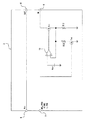
図1に示すように、光源点灯回路1は、第1の制御端子4及び第2の制御端子5を有する逆流防止部2と、共通端子6及び切替端子7を有する電流制御部3とを備えて構成されている。
As shown in FIG. 1, the light
逆流防止部2は、第1のPチャネルFET(以下、「PMOSトランジスタTr1」と呼ぶ。)と、第2のPチャネルFET(以下、「PMOSトランジスタTr2」と呼ぶ。)と、NPNトランジスタTr3、Tr4(スイッチ駆動回路)とを備えて構成されている。逆流防止部2は、第1の制御端子4の電圧をダイオードD1(第1の整流素子)を介して切替端子7に出力する。逆流防止部2は、第2の制御端子5の電圧をダイオードD2(第2の整流素子)を介して共通端子6に出力する。
The backflow prevention unit 2 includes a first P-channel FET (hereinafter referred to as “PMOS transistor Tr1”), a second P-channel FET (hereinafter referred to as “PMOS transistor Tr2”), an NPN transistor Tr3, Tr4 (switch drive circuit). The backflow prevention unit 2 outputs the voltage of the first control terminal 4 to the
PMOSトランジスタTr1はドレインが第1の制御端子4に接続され、ソースが共通端子6に接続され、ゲートが抵抗R1とダイオードD4(第3の整流素子)を介してPMOSトランジスタTr2のドレインに接続されている。ソース−ドレイン間には寄生ダイオードD3が存在している。 The PMOS transistor Tr1 has a drain connected to the first control terminal 4, a source connected to the common terminal 6, and a gate connected to the drain of the PMOS transistor Tr2 via a resistor R1 and a diode D4 (third rectifier element). ing. A parasitic diode D3 exists between the source and the drain.
抵抗R1は一端が第1接続点N1を介してPMOSトランジスタTr1のゲートに接続され他端がPMOSトランジスタTr2及びダイオードD2(第2整流素子)の第2接続点N2に接続されている。 One end of the resistor R1 is connected to the gate of the PMOS transistor Tr1 via the first connection point N1, and the other end is connected to the second connection point N2 of the PMOS transistor Tr2 and the diode D2 (second rectifier element).
抵抗R2(第2の抵抗)は一端が第1接続点N1を介してPMOSトランジスタTr1のゲート及び抵抗R1の一端に接続され、他端が接地されている。抵抗R2の抵抗値は抵抗R1の抵抗値よりも大きい。尚、第1接続点N1とPMOSトランジスタTr1のソースの間に電位差発生素子(ツェナーダイオード又は抵抗)を接続してもよい。 One end of the resistor R2 (second resistor) is connected to the gate of the PMOS transistor Tr1 and one end of the resistor R1 via the first connection point N1, and the other end is grounded. The resistance value of the resistor R2 is larger than the resistance value of the resistor R1. A potential difference generating element (zener diode or resistor) may be connected between the first connection point N1 and the source of the PMOS transistor Tr1.
PMOSトランジスタTr2はドレインがダイオードD2を介して共通端子6に接続され、ソースが第2の制御端子5に接続され、ゲートがダイオードD5と抵抗R4を介してNPNトランジスタTr3のコレクタに接続されている。ソース−ドレイン間には寄生ダイオードD6が存在している。PMOSトランジスタTr2とダイオードD2は直列に接続されている。 The PMOS transistor Tr2 has a drain connected to the common terminal 6 via the diode D2, a source connected to the second control terminal 5, and a gate connected to the collector of the NPN transistor Tr3 via the diode D5 and the resistor R4. . A parasitic diode D6 exists between the source and the drain. The PMOS transistor Tr2 and the diode D2 are connected in series.
NPNトランジスタTr3はエミッタが接地され、ベースが抵抗R6を介してNPNトランジスタTr4のコレクタに接続されている。ベース−エミッタ間には抵抗R7が接続されている。 The NPN transistor Tr3 has an emitter grounded and a base connected to the collector of the NPN transistor Tr4 via a resistor R6. A resistor R7 is connected between the base and the emitter.
NPNトランジスタTr4はエミッタが接地され、ベースが抵抗R8及びダイオードD1を介して第1の制御端子4に接続され、コレクタは抵抗R5及びダイオードD7を介して第2の制御端子5及びPMOSトランジスタTr2のソースに接続されている。ベース−エミッタ間には抵抗R9が接続されている。 The NPN transistor Tr4 has an emitter grounded, a base connected to the first control terminal 4 via the resistor R8 and the diode D1, and a collector connected to the second control terminal 5 and the PMOS transistor Tr2 via the resistor R5 and the diode D7. Connected to the source. A resistor R9 is connected between the base and the emitter.
電流制御部3は、共通端子6、切替端子7、出力端子8及び入力端子9を含んで構成され、直列に接続された光源としてのLED(Light Emitting Diode)40、40、40に出力端子8を介して駆動電流を供給する。
The
以下の説明では、デイタイムランニングランプを点灯させるための駆動電流を第1の駆動電流I1(第1の電流に対応する電流)と呼び、ポジションランプを点灯させるための駆動電流を第2の駆動電流I2(第2の電流に対応する電流)と呼ぶ。 In the following description, the driving current for lighting the daytime running lamp is referred to as a first driving current I1 (current corresponding to the first current), and the driving current for lighting the position lamp is the second driving. This is called current I2 (current corresponding to the second current).
電流制御部3は、第1の例として、LED40、40、40のカソード側にオペアンプ及びNMOSトランジスタを含む定電流クランプ回路が用いられている(図2参照)。定電流クランプ回路は、LED40、40、40の駆動電流に対応した駆動電圧をフィードバックして、予め設定された基準電圧になるように駆動電流を安定的に制御する機能を有する。
As a first example, the
定電流クランプ回路は、オペアンプ13とNMOSトランジスタTr5、Tr6と抵抗R12、R13を備えて構成されている。
The constant current clamp circuit includes an
切替端子7はNMOSトランジスタTr6のゲートに接続されている。NMOSトランジスタTr6はドレインが抵抗R13を介してオペアンプ13の反転入力端子に接続されソースが接地されている。オペアンプ13の非反転入力端子には所定の基準電圧Vrefが入力される。オペアンプ13の出力はNMOSトランジスタTr5のゲートに入力される。NMOSトランジスタTr5はドレインが入力端子9に接続されソースが抵抗R12、R13の一端に接続されている。
The switching
また、電流制御部3は、第2の例として、PWMコンパレータ、エラーアンプ及びNMOSトランジスタを含むスイッチングレギュレータ回路が用いられたものであってもよい(図3参照)。スイッチングレギュレータ回路は、LED40、40、40に供給される第1の駆動電流I1又は第2の駆動電流I2にそれぞれ対応した第1の駆動電圧又は第2の駆動電圧をフィードバックして、第1の駆動電圧又は第2の駆動電圧が予め設定された基準電圧になるようにスイッチング素子を高速にスイッチングすると共に該スイッチング素子のオン/オフのデューティ比を変化させる。即ち、スイッチングレギュレータ回路はLED40、40、40に供給される第1の駆動電流I1又は第2の駆動電流I2を安定的に制御する機能を有する。
Moreover, the
スイッチングレギュレータ回路は、コンデンサC1、C2、チョークコイルL、NMOSトランジスタTr7、Tr8、PWMコンパレータ22、エラーアンプ23及び抵抗R14、15を備えて構成されている。
The switching regulator circuit includes capacitors C1 and C2, a choke coil L, NMOS transistors Tr7 and Tr8, a
共通端子6はコンデンサC1及びチョークコイルLに接続されている。共通端子6からの第1の駆動電流I1又は第2の駆動電流I2はチョークコイルL及びダイオードD8を介して出力端子8に供給される。
The common terminal 6 is connected to the capacitor C1 and the choke coil L. The first drive current I1 or the second drive current I2 from the common terminal 6 is supplied to the
切替端子7はNMOSトランジスタTr7のゲートに接続されている。NMOSトランジスタTr7はドレインが抵抗R15を介してエラーアンプ23の反転入力端子及び入力端子9に接続されソースが接地されている。入力端子9は抵抗R14、抵抗R15の一端に接続される。エラーアンプ23の非反転入力端子には所定の基準電圧Vrefが入力されている。エラーアンプ23の出力はPWMコンパレータ22に入力される。PWMコンパレータ22の出力はNMOSトランジスタTr8のゲートに入力される。NMOSトランジスタTr8はドレインがチョークコイルL及びダイオードD8に接続されソースが接地されている。
The switching
逆流防止部2とバッテリ(直流電源+B)の間には、オンオフ機能を有するスイッチSW1及びスイッチSW2が接続されている(図1参照)。スイッチSW1のみをオンすると直流電源電圧が第1の制御端子4に送出され第1の駆動電流I1がLED40、40、40に供給される。スイッチSW2のみをオンすると直流電源電圧が第2の制御端子5に送出され第2の駆動電流I2がLED40、40、40に供給される。スイッチSW1及びスイッチSW2を同時にオンすると直流電源電圧が第1の制御端子4及び第2の制御端子5に送出され第1の駆動電流I1がLED40、40、40に供給される。
A switch SW1 and a switch SW2 having an on / off function are connected between the backflow prevention unit 2 and the battery (DC power supply + B) (see FIG. 1). When only the switch SW1 is turned on, the DC power supply voltage is sent to the first control terminal 4 and the first drive current I1 is supplied to the
尚、光源点灯回路1内には複数のアース端子が設けられているが、全てのアース端子は電気的に接続されている。
Although a plurality of ground terminals are provided in the light
以下に、光源点灯回路1の動作についてスイッチSW1のみをオンする場合(A)とスイッチSW2のみをオンする場合(B)とスイッチSW1及びスイッチSW2を同時にオンする場合(C)とに分けて説明する。
Hereinafter, the operation of the light
(A)まず、スイッチSW1のみをオンする場合の点灯制御回路1の動作について説明する。
(A) First, the operation of the
スイッチSW1のみがオンすると、第1の制御端子4に直流電源電圧(+B)が入力され、第2の制御端子5には直流電源電圧(+B)は入力されず、直流電源電圧(制御信号)は第1の制御端子4を介して寄生ダイオードD3及びNPNトランジスタTr4のベースに送出される。寄生ダイオードD3には電流が流れてPMOSトランジスタTr1のゲート−ソース間に電位差が生じPMOSトランジスタTr1がオンする。その際、切替端子7の出力がハイレベルとなっているので共通端子6には第1の電流が供給される。
When only the switch SW1 is turned on, the DC power supply voltage (+ B) is input to the first control terminal 4, and the DC power supply voltage (+ B) is not input to the second control terminal 5, but the DC power supply voltage (control signal). Is sent to the base of the parasitic diode D3 and the NPN transistor Tr4 via the first control terminal 4. A current flows through the parasitic diode D3, causing a potential difference between the gate and source of the PMOS transistor Tr1, and the PMOS transistor Tr1 is turned on. At this time, since the output of the switching
NPNトランジスタTr4はダイオードD1を介して直流電源電圧(制御信号)を受けてオンする。NPNトランジスタTr4がオンするとNPNトランジスタTr3がオフする。従って、抵抗R3には電位差が発生せずPMOSトランジスタTr2のゲート−ソース電圧が発生しないためPMOSトランジスタTr2がオフする。従って、PMOSトランジスタTr1のゲートには電圧が印加されないのでPMOSトランジスタTr1はオンを維持する。従って、第1の駆動電流I1はPMOSトランジスタTr1を通過して共通端子6に送出される。 The NPN transistor Tr4 is turned on by receiving a DC power supply voltage (control signal) via the diode D1. When the NPN transistor Tr4 is turned on, the NPN transistor Tr3 is turned off. Accordingly, no potential difference is generated in the resistor R3, and no gate-source voltage of the PMOS transistor Tr2 is generated, so that the PMOS transistor Tr2 is turned off. Accordingly, no voltage is applied to the gate of the PMOS transistor Tr1, so that the PMOS transistor Tr1 remains on. Accordingly, the first drive current I1 passes through the PMOS transistor Tr1 and is sent to the common terminal 6.
また、直流電源電圧はダイオードD1を介して切替端子7に入力される。
The DC power supply voltage is input to the switching
以下に、切替端子7に直流電源電圧が入力された後の電流制御部3の動作について、電流制御部3が定電流クランプ回路を用いたものである場合(図2参照)と電流制御部3がスイッチングレギュレータ回路を用いたものである場合(図3参照)とに分けて説明する。
Hereinafter, regarding the operation of the
電流制御部3が定電流クランプ回路を用いたものである場合には、切替端子7に入力された直流電源電圧はNMOSトランジスタTr6のゲートに入力されNMOSトランジスタTr6がオンする。
When the
NMOSトランジスタTr6がオンすると、NMOSトランジスタTr5のドレイン−ソース間を流れる第1の駆動電流の電流値I1は抵抗R13及び抵抗R12の並列接続による抵抗によって発生する電圧降下分と基準電圧Vrefとが同じ値になるように制御される。このようにして第1の駆動電流I1が一定になるように制御される。 When the NMOS transistor Tr6 is turned on, the current value I1 of the first drive current flowing between the drain and source of the NMOS transistor Tr5 is the same as the reference voltage Vref and the voltage drop caused by the resistance due to the parallel connection of the resistors R13 and R12. It is controlled to become a value. In this way, the first drive current I1 is controlled to be constant.
電流制御部3がスイッチングレギュレータ回路を用いたものである場合には、切替端子7に入力された直流電源電圧はNMOSトランジスタTr7のゲートに入力されNMOSトランジスタTr7がオンする。
When the
NMOSトランジスタTr7がオンすると、入力端子9から送出される第1の駆動電流の電流値I1に対し抵抗R14及び抵抗R15の並列接続による抵抗によって発生する電圧降下分である第1の駆動電圧がエラーアンプ23の反転入力端子に入力される。第1の駆動電圧が予め設定された基準電圧Vrefになるようにエラーアンプ23からエラーアンプ出力がPWMコンパレータ22に送出される。PWMコンパレータ22では予め設定されたノコギリ波とエラーアンプ出力とによって決定されるオンオフのデューティ比に基いてNMOSトランジスタTr8を高速にオンオフさせる。このようにして第1の駆動電圧をフィードバックして、第1の駆動電圧が予め設定された基準電圧VrefになるようにNMOSトランジスタTr8を制御して第1の駆動電流I1を一定にしている。
When the NMOS transistor Tr7 is turned on, the first drive voltage, which is a voltage drop caused by the resistance due to the parallel connection of the resistor R14 and the resistor R15 with respect to the current value I1 of the first drive current sent from the
(B)次に、スイッチSW2のみをオンする場合の点灯制御回路1の動作について説明する。
(B) Next, the operation of the
スイッチSW1がオフしスイッチSW2がオンすると、第1の制御端子4には直流電源電圧(+B)が入力されず、第2の制御端子5に直流電源電圧(+B)が入力され、NPNトランジスタTr4がオフし、直流電源電圧(制御信号)が第2の制御端子5、抵抗R5及び抵抗R6を介してNPNトランジスタTr3のベースに送出されNPNトランジスタTr3がオンする。 When the switch SW1 is turned off and the switch SW2 is turned on, the DC power supply voltage (+ B) is not input to the first control terminal 4, the DC power supply voltage (+ B) is input to the second control terminal 5, and the NPN transistor Tr4 Is turned off, and the DC power supply voltage (control signal) is sent to the base of the NPN transistor Tr3 via the second control terminal 5, the resistor R5 and the resistor R6, and the NPN transistor Tr3 is turned on.
NPNトランジスタTr3がオンすると抵抗R3には電位差が発生しPMOSトランジスタTr2のゲート−ソース電圧が発生するためPMOSトランジスタTr2がオンする。 When the NPN transistor Tr3 is turned on, a potential difference is generated in the resistor R3 and the gate-source voltage of the PMOS transistor Tr2 is generated, so that the PMOS transistor Tr2 is turned on.
PMOSトランジスタTr2がオンすると電流制御部3の切替端子7の出力がローレベルとなるのでダイオードD2を介して共通端子6に第2の電流が供給される。
When the PMOS transistor Tr2 is turned on, the output of the switching
ダイオードD4を介してPMOSトランジスタTr1のゲートに電圧が印加されるのでPMOSトランジスタTr1はオフする。尚、第2の制御端子5を逆接続したとき又は第2の制御端子の電圧が0ボルトであるときでも、ダイオードD4の存在によって逆流防止部2内に流れる逆電流を遮断することができる。 Since a voltage is applied to the gate of the PMOS transistor Tr1 via the diode D4, the PMOS transistor Tr1 is turned off. Even when the second control terminal 5 is reversely connected or when the voltage of the second control terminal is 0 volts, the reverse current flowing in the backflow prevention unit 2 can be blocked by the presence of the diode D4.
また、直流電源電圧は切替端子7に入力されない。
Further, the DC power supply voltage is not input to the switching
電流制御部3が定電流クランプ回路を用いたものである場合(図2参照)には、切替端子7に直流電源電圧が入力されないのでNMOSトランジスタTr6がオフする。
When the
NMOSトランジスタTr6がオフすると、NMOSトランジスタTr5のドレイン−ソース間を流れる第2の駆動電流I2の電流値は抵抗R12によって発生する電圧降下分と基準電圧Vrefとが同じ値になるように制御される。このようにして第2の駆動電流I2が一定になるように制御される。 When the NMOS transistor Tr6 is turned off, the current value of the second drive current I2 flowing between the drain and source of the NMOS transistor Tr5 is controlled so that the voltage drop generated by the resistor R12 and the reference voltage Vref have the same value. . In this way, the second drive current I2 is controlled to be constant.
電流制御部3がスイッチングレギュレータ回路を用いたものである場合(図3参照)には、切替端子7に直流電源電圧が入力されないのでNMOSトランジスタTr7がオフする。
When the
NMOSトランジスタTr7がオフすると、入力端子9から送出される第2の駆動電流I2の電流値に対し抵抗R14によって発生する電圧降下分である第2の駆動電圧がエラーアンプ23の反転入力端子に入力される。第2の駆動電圧が予め設定された基準電圧Vrefになるようにエラーアンプ23からエラーアンプ出力がPWMコンパレータ22に送出される。PWMコンパレータ22では予め設定されたノコギリ波とエラーアンプ出力とによって決定されるオンオフのデューティ比に基いてNMOSトランジスタTr8を高速にオンオフさせる。このようにして第2の駆動電圧をフィードバックして、第2の駆動電圧が予め設定された基準電圧VrefになるようにNMOSトランジスタTr8を制御して第2の駆動電流I2を一定にしている。
When the NMOS transistor Tr7 is turned off, the second drive voltage, which is a voltage drop generated by the resistor R14 with respect to the current value of the second drive current I2 sent from the
NMOSトランジスタTr6又はNMOSトランジスタTr7がオンすることにより、抵抗R12又は抵抗R14の両端の抵抗値はNMOSトランジスタTr6又はNMOSトランジスタTr7がオフの時より小さな値に変化するため、第1の駆動電流の電流値I1は第2の駆動電流の電流値I2より大きい値となるように制御される。 When the NMOS transistor Tr6 or the NMOS transistor Tr7 is turned on, the resistance value at both ends of the resistor R12 or the resistor R14 changes to a smaller value than when the NMOS transistor Tr6 or the NMOS transistor Tr7 is turned off. The value I1 is controlled to be larger than the current value I2 of the second drive current.
(C)次に、スイッチSW1及びスイッチSW2を同時にオンする場合の点灯制御回路1の動作について説明する。
(C) Next, the operation of the
スイッチSW1及びスイッチSW2が同時にオンすると、第1の制御端子4及び第2の制御端子5に直流電源電圧(+B)が入力され、直流電源電圧は第1の制御端子4を介して寄生ダイオードD3及びダイオードD1を介して電流制御部3の切替端子7に送出される。寄生ダイオードD3には電流が流れてPMOSトランジスタTr1のゲート−ソース間に電位差が生じPMOSトランジスタTr1がオンする。その際、切替端子7の出力がハイレベルとなっているので共通端子6には第1の電流が供給される。
When the switch SW1 and the switch SW2 are simultaneously turned on, the DC power supply voltage (+ B) is input to the first control terminal 4 and the second control terminal 5, and the DC power supply voltage is parasitic diode D3 via the first control terminal 4. And sent to the switching
NPNトランジスタTr4はダイオードD1を介して直流電源電圧(制御信号)を受けてオンする。NPNトランジスタTr4がオンするとNPNトランジスタTr3がオフする。 The NPN transistor Tr4 is turned on by receiving a DC power supply voltage (control signal) via the diode D1. When the NPN transistor Tr4 is turned on, the NPN transistor Tr3 is turned off.
スイッチSW2もオンしているがNPNトランジスタTr4がオンしているのでNPNトランジスタTr3がオフする。NPNトランジスタTr3がオフすると抵抗R3には電位差が発生しないのでPMOSトランジスタTr2のゲート−ソース電圧が発生せずにPMOSトランジスタTr2がオフする。 Although the switch SW2 is also on, the NPN transistor Tr3 is turned off because the NPN transistor Tr4 is on. When the NPN transistor Tr3 is turned off, no potential difference is generated in the resistor R3, so that the gate-source voltage of the PMOS transistor Tr2 is not generated and the PMOS transistor Tr2 is turned off.
PMOSトランジスタTr2がオフするので共通端子6に第2の駆動電流I2が供給されることはない。従って、第1の駆動電流(I1)はPMOSトランジスタTr1を通過して共通端子6に送出される。 Since the PMOS transistor Tr2 is turned off, the second drive current I2 is not supplied to the common terminal 6. Accordingly, the first drive current (I1) is sent to the common terminal 6 through the PMOS transistor Tr1.
電流制御部3が定電流クランプ回路を用いたものである場合(図2参照)と電流制御部3がスイッチングレギュレータ回路を用いたものである場合(図3参照)については、上記したスイッチSW1のみオンする場合と同様であるので説明は省略する。
When the
以上に説明したように、光源点灯回路1は、スイッチSW1及びスイッチSW2を同時にオンする場合においてもスイッチSW1のみをオンする場合と同様の動作がされるのでデイタイムランニングランプとして機能させる第1の駆動電流I1の送出が優先される。
As described above, the light
デイタイムランニングランプ及びポジショニングランプの機能を共通の光源にて実現させ、かつデイタイムランニングランプを優先させたときでも、逆流防止手段としてオン抵抗の少ないPMOSトランジスタを用いているので、逆流防止部の回路損失の増大及び発熱を抑制するとともにバッテリの逆接続に起因する逆流の防止を図ることができる。 Even when the functions of the daytime running lamp and the positioning lamp are realized with a common light source and the daytime running lamp is prioritized, a PMOS transistor with low on-resistance is used as a backflow prevention means. It is possible to suppress an increase in circuit loss and heat generation, and to prevent backflow due to reverse battery connection.
また、逆流防止手段として、ダイオードと比較してコストの低いPMOSトランジスタを用いているので、光源点灯回路及びこれを備えた車両用灯具システムの製品コストの低減を図るとともにバッテリの逆接続に起因する逆流の防止を図ることができる。 In addition, since a PMOS transistor, which is less expensive than a diode, is used as a backflow prevention means, the product cost of the light source lighting circuit and the vehicle lamp system including the light source lighting circuit is reduced and the battery is reversely connected. Backflow can be prevented.
上記した実施の形態は、本発明を好適に実施した形態の一例に過ぎず、本発明は、その主旨を逸脱しない限り、種々変形して実施することが可能なものである。 The above-described embodiment is merely an example of a preferred embodiment of the present invention, and the present invention can be implemented with various modifications without departing from the gist thereof.
1…光源点灯回路、2…逆流防止部、3…電流制御部、4…第1の制御端子、5…第2の制御端子、6…共通端子、7…切替端子、40、40、40…LED(光源)
DESCRIPTION OF
Claims (5)
前記第1の制御端子及び前記第2の制御端子に接続される共通端子と、前記第1の制御端子に接続される切替端子とを有し、前記光源に対して前記共通端子からそれぞれ前記第1の電流又は前記第2の電流に対応する第1の駆動電流又は第2の駆動電流を供給する電流制御部とを備え、
前記逆流防止部は、前記第1の制御端子の電圧を第1の整流素子を介して前記切替端子に出力し、
前記第1の制御端子と前記共通端子の間に第1のPチャネルFETが接続され、
前記第2の制御端子と前記共通端子の間に第2のPチャネルFET及び第2の整流素子が直列に接続され、前記第2のPチャネルFETが前記第2の整流素子より前記第2の制御端子側に配置されるように接続され、
前記第1の制御端子に直流電源電圧が入力されたときに、前記第1のPチャネルFETがオンし第2のPチャネルFETがオフして前記第1の電流が送出され、
前記第1の制御端子に前記直流電源電圧が入力されず、かつ、前記第2の制御端子に前記直流電源電圧が入力されたときに、前記第2のPチャネルFETがオンして前記第2の電流が送出される
ことを特徴とする光源点灯回路。 A backflow prevention unit that has a first control terminal and a second control terminal, and sends a first current or a second current smaller than the first current to the light source;
A common terminal connected to the first control terminal and the second control terminal; and a switching terminal connected to the first control terminal. A current control unit that supplies a first drive current or a second drive current corresponding to one current or the second current;
The backflow prevention unit outputs the voltage of the first control terminal to the switching terminal via a first rectifier element,
A first P-channel FET is connected between the first control terminal and the common terminal;
A second P-channel FET and a second rectifier element are connected in series between the second control terminal and the common terminal, and the second P-channel FET is connected to the second rectifier element by the second rectifier element. Connected to be placed on the control terminal side,
When a DC power supply voltage is input to the first control terminal, the first P-channel FET is turned on and the second P-channel FET is turned off to send the first current,
When the DC power supply voltage is not input to the first control terminal and the DC power supply voltage is input to the second control terminal, the second P-channel FET is turned on and the second control channel is turned on. The light source lighting circuit is characterized by the fact that the current is sent out.
一端が前記第1接続点に接続され他端が接地された第2の抵抗とを有し、
前記第2の抵抗の抵抗値が前記第1の抵抗の抵抗値よりも大きい
ことを特徴とする請求項1に記載の光源点灯回路。 One end is connected to a first connection point that is a gate terminal of the first P-channel FET, and the other end is connected to a second connection point of the second P-channel FET and the second rectifier element. Resistance,
A second resistor having one end connected to the first connection point and the other end grounded;
The light source lighting circuit according to claim 1, wherein a resistance value of the second resistor is larger than a resistance value of the first resistor.
ことを特徴とする請求項2に記載の光源点灯回路。 The light source lighting circuit according to claim 2, wherein a third rectifier element is connected in series with the first resistor between the first connection point and the second connection point.
ことを特徴とする請求項1、請求項2又は請求項3に記載の光源点灯回路。 2. A switch drive circuit that receives a control signal from the first control terminal and the second control terminal and sends a switch drive signal to a gate terminal of the second P-channel FET. The light source lighting circuit according to claim 2.
ことを特徴とする車両用灯具システム。 A vehicle lamp system comprising the light source and the light source lighting circuit according to claim 1, claim 2, claim 3, or claim 4.
Priority Applications (3)
| Application Number | Priority Date | Filing Date | Title |
|---|---|---|---|
| JP2010176196A JP5571496B2 (en) | 2010-08-05 | 2010-08-05 | Light source lighting circuit and vehicle lamp system |
| EP11176694.5A EP2416626B1 (en) | 2010-08-05 | 2011-08-05 | Light source lighting circuit and lamp system for vehicle |
| US13/198,987 US8476838B2 (en) | 2010-08-05 | 2011-08-05 | Light source lighting circuit and lamp system for vehicle |
Applications Claiming Priority (1)
| Application Number | Priority Date | Filing Date | Title |
|---|---|---|---|
| JP2010176196A JP5571496B2 (en) | 2010-08-05 | 2010-08-05 | Light source lighting circuit and vehicle lamp system |
Publications (2)
| Publication Number | Publication Date |
|---|---|
| JP2012038496A JP2012038496A (en) | 2012-02-23 |
| JP5571496B2 true JP5571496B2 (en) | 2014-08-13 |
Family
ID=44903059
Family Applications (1)
| Application Number | Title | Priority Date | Filing Date |
|---|---|---|---|
| JP2010176196A Active JP5571496B2 (en) | 2010-08-05 | 2010-08-05 | Light source lighting circuit and vehicle lamp system |
Country Status (3)
| Country | Link |
|---|---|
| US (1) | US8476838B2 (en) |
| EP (1) | EP2416626B1 (en) |
| JP (1) | JP5571496B2 (en) |
Families Citing this family (6)
| Publication number | Priority date | Publication date | Assignee | Title |
|---|---|---|---|---|
| CN103863172B (en) * | 2012-12-12 | 2016-05-04 | 北汽福田汽车股份有限公司 | A kind of car light controller and there is its automobile |
| JP6101587B2 (en) * | 2013-07-18 | 2017-03-22 | 株式会社小糸製作所 | Vehicle headlamp |
| CN104466886B (en) * | 2013-09-18 | 2018-08-10 | 鸿富锦精密工业(深圳)有限公司 | Load protection circuit and load protective method |
| ITMI20131902A1 (en) * | 2013-11-15 | 2015-05-16 | Campagnolo Srl | ELECTRONIC BICYCLE SYSTEM |
| JP6531941B2 (en) * | 2015-07-08 | 2019-06-19 | パナソニックIpマネジメント株式会社 | Circuit device, lighting device, and vehicle using the same |
| FR3070572B1 (en) * | 2017-08-31 | 2022-03-25 | Valeo Vision | DEVICE FOR CONTROLLING THE POWER SUPPLY OF LIGHT SOURCES COMPRISING SEVERAL PROTECTED INPUTS |
Family Cites Families (11)
| Publication number | Priority date | Publication date | Assignee | Title |
|---|---|---|---|---|
| US5821699A (en) * | 1994-09-30 | 1998-10-13 | Pacific Scientific | Ballast circuit for fluorescent lamps |
| JPH08308217A (en) * | 1995-04-27 | 1996-11-22 | Canon Inc | Dc-dc converter |
| US5872430A (en) * | 1996-08-14 | 1999-02-16 | Motorola Inc. | Single switch electronic ballast with low in-rush current |
| JP2003037933A (en) * | 2001-07-24 | 2003-02-07 | Koito Mfg Co Ltd | Protection apparatus of electronic equipment |
| JP4256136B2 (en) * | 2002-10-01 | 2009-04-22 | 株式会社小糸製作所 | Vehicle lighting |
| JP2004136719A (en) * | 2002-10-15 | 2004-05-13 | Koito Mfg Co Ltd | Lighting circuit |
| JP2005029020A (en) * | 2003-07-14 | 2005-02-03 | Ichikoh Ind Ltd | Switching circuit and electronic light emitting element driving circuit for lighting fixture for vehicle |
| JP2006073352A (en) * | 2004-09-02 | 2006-03-16 | Koito Mfg Co Ltd | Lighting control circuit of vehicular luminair |
| US7656103B2 (en) * | 2006-01-20 | 2010-02-02 | Exclara, Inc. | Impedance matching circuit for current regulation of solid state lighting |
| TW200808124A (en) * | 2006-07-20 | 2008-02-01 | Ind Tech Res Inst | Single-stage electronic ballast circuit |
| US7906913B2 (en) * | 2008-04-18 | 2011-03-15 | Osram Sylvania Inc. | Low loss input channel detection device for a direct current powered lighting system |
-
2010
- 2010-08-05 JP JP2010176196A patent/JP5571496B2/en active Active
-
2011
- 2011-08-05 US US13/198,987 patent/US8476838B2/en active Active
- 2011-08-05 EP EP11176694.5A patent/EP2416626B1/en active Active
Also Published As
| Publication number | Publication date |
|---|---|
| US8476838B2 (en) | 2013-07-02 |
| US20120032591A1 (en) | 2012-02-09 |
| EP2416626A3 (en) | 2013-10-09 |
| EP2416626B1 (en) | 2018-10-10 |
| EP2416626A2 (en) | 2012-02-08 |
| JP2012038496A (en) | 2012-02-23 |
Similar Documents
| Publication | Publication Date | Title |
|---|---|---|
| JP5571496B2 (en) | Light source lighting circuit and vehicle lamp system | |
| JP6259649B2 (en) | Vehicle lighting | |
| JP5301976B2 (en) | Control device for vehicular lamp | |
| US8729821B2 (en) | Semiconductor light source lighting circuit and control method | |
| US10383185B2 (en) | Motor vehicle illumination device | |
| WO2016125561A1 (en) | Switching power supply device | |
| JP2016197711A (en) | Drive circuit and vehicle lighting device | |
| JP5396075B2 (en) | Control device for vehicular lamp | |
| JP4872582B2 (en) | Load drive circuit | |
| JP5280182B2 (en) | Vehicle lighting | |
| WO2015145733A1 (en) | Vehicle-mounted device | |
| JP5187756B2 (en) | Light emitting device for vehicle lamp | |
| JP2013159288A (en) | Vehicular lamp | |
| US20070273346A1 (en) | Voltage regulator circuit with over-current protection | |
| US20170271986A1 (en) | Switching regulator | |
| JP4821394B2 (en) | Semiconductor device drive circuit | |
| JP2011100837A (en) | Self-excitation type led driving circuit | |
| JP6191149B2 (en) | LED lighting circuit for vehicle lighting | |
| JP6139360B2 (en) | Light source drive device | |
| JP2011087389A (en) | Dc-dc converter and lamp fitting for vehicles | |
| JP6181718B2 (en) | Light source drive device | |
| US11839003B2 (en) | Apparatus for supplying power to drive alternating current (AC) direct-coupled light-emitting diodes (LED) | |
| US11229100B2 (en) | Light source driving device and method therefor | |
| JP2011114217A (en) | Led drive circuit | |
| JP6580794B1 (en) | In-vehicle LED lighting control device and control method of in-vehicle LED lighting control device |
Legal Events
| Date | Code | Title | Description |
|---|---|---|---|
| A621 | Written request for application examination |
Free format text: JAPANESE INTERMEDIATE CODE: A621 Effective date: 20130703 |
|
| A977 | Report on retrieval |
Free format text: JAPANESE INTERMEDIATE CODE: A971007 Effective date: 20140224 |
|
| TRDD | Decision of grant or rejection written | ||
| A01 | Written decision to grant a patent or to grant a registration (utility model) |
Free format text: JAPANESE INTERMEDIATE CODE: A01 Effective date: 20140603 |
|
| A61 | First payment of annual fees (during grant procedure) |
Free format text: JAPANESE INTERMEDIATE CODE: A61 Effective date: 20140626 |
|
| R150 | Certificate of patent or registration of utility model |
Ref document number: 5571496 Country of ref document: JP Free format text: JAPANESE INTERMEDIATE CODE: R150 |