JP5554635B2 - Integrated circuit package frame structure and manufacturing method thereof - Google Patents
Integrated circuit package frame structure and manufacturing method thereof Download PDFInfo
- Publication number
- JP5554635B2 JP5554635B2 JP2010129720A JP2010129720A JP5554635B2 JP 5554635 B2 JP5554635 B2 JP 5554635B2 JP 2010129720 A JP2010129720 A JP 2010129720A JP 2010129720 A JP2010129720 A JP 2010129720A JP 5554635 B2 JP5554635 B2 JP 5554635B2
- Authority
- JP
- Japan
- Prior art keywords
- frame structure
- circuit package
- integrated circuit
- frame
- flange
- Prior art date
- Legal status (The legal status is an assumption and is not a legal conclusion. Google has not performed a legal analysis and makes no representation as to the accuracy of the status listed.)
- Expired - Lifetime
Links
- 238000004519 manufacturing process Methods 0.000 title claims description 29
- 239000000463 material Substances 0.000 claims description 61
- OKTJSMMVPCPJKN-UHFFFAOYSA-N Carbon Chemical compound [C] OKTJSMMVPCPJKN-UHFFFAOYSA-N 0.000 claims description 33
- 239000010439 graphite Substances 0.000 claims description 33
- 229910002804 graphite Inorganic materials 0.000 claims description 33
- 239000000203 mixture Substances 0.000 claims description 31
- 229920000106 Liquid crystal polymer Polymers 0.000 claims description 30
- 239000004977 Liquid-crystal polymers (LCPs) Substances 0.000 claims description 29
- 238000000034 method Methods 0.000 claims description 27
- FJKROLUGYXJWQN-UHFFFAOYSA-N 4-hydroxybenzoic acid Chemical compound OC(=O)C1=CC=C(O)C=C1 FJKROLUGYXJWQN-UHFFFAOYSA-N 0.000 claims description 14
- 229940090248 4-hydroxybenzoic acid Drugs 0.000 claims description 7
- KKEYFWRCBNTPAC-UHFFFAOYSA-N Terephthalic acid Chemical compound OC(=O)C1=CC=C(C(O)=O)C=C1 KKEYFWRCBNTPAC-UHFFFAOYSA-N 0.000 claims description 6
- 238000002844 melting Methods 0.000 claims description 5
- 230000008018 melting Effects 0.000 claims description 5
- IISBACLAFKSPIT-UHFFFAOYSA-N bisphenol A Chemical compound C=1C=C(O)C=CC=1C(C)(C)C1=CC=C(O)C=C1 IISBACLAFKSPIT-UHFFFAOYSA-N 0.000 claims description 4
- 238000002347 injection Methods 0.000 claims description 4
- 239000007924 injection Substances 0.000 claims description 4
- XNGIFLGASWRNHJ-UHFFFAOYSA-N phthalic acid Chemical compound OC(=O)C1=CC=CC=C1C(O)=O XNGIFLGASWRNHJ-UHFFFAOYSA-N 0.000 claims description 4
- KAUQJMHLAFIZDU-UHFFFAOYSA-N 6-Hydroxy-2-naphthoic acid Chemical compound C1=C(O)C=CC2=CC(C(=O)O)=CC=C21 KAUQJMHLAFIZDU-UHFFFAOYSA-N 0.000 claims description 3
- 229930185605 Bisphenol Natural products 0.000 claims description 2
- 229920001577 copolymer Polymers 0.000 claims description 2
- 229920001897 terpolymer Polymers 0.000 claims 1
- RYGMFSIKBFXOCR-UHFFFAOYSA-N Copper Chemical compound [Cu] RYGMFSIKBFXOCR-UHFFFAOYSA-N 0.000 description 36
- 229910052802 copper Inorganic materials 0.000 description 36
- 239000010949 copper Substances 0.000 description 36
- 229910045601 alloy Inorganic materials 0.000 description 25
- 239000000956 alloy Substances 0.000 description 25
- XEEYBQQBJWHFJM-UHFFFAOYSA-N Iron Chemical compound [Fe] XEEYBQQBJWHFJM-UHFFFAOYSA-N 0.000 description 19
- PXHVJJICTQNCMI-UHFFFAOYSA-N Nickel Chemical compound [Ni] PXHVJJICTQNCMI-UHFFFAOYSA-N 0.000 description 18
- 230000008569 process Effects 0.000 description 16
- 238000005476 soldering Methods 0.000 description 16
- OAICVXFJPJFONN-UHFFFAOYSA-N Phosphorus Chemical compound [P] OAICVXFJPJFONN-UHFFFAOYSA-N 0.000 description 11
- 239000011574 phosphorus Substances 0.000 description 11
- 229910052698 phosphorus Inorganic materials 0.000 description 11
- PCHJSUWPFVWCPO-UHFFFAOYSA-N gold Chemical compound [Au] PCHJSUWPFVWCPO-UHFFFAOYSA-N 0.000 description 10
- 229910052737 gold Inorganic materials 0.000 description 10
- 239000010931 gold Substances 0.000 description 10
- 238000000465 moulding Methods 0.000 description 10
- 238000001746 injection moulding Methods 0.000 description 9
- 229910052742 iron Inorganic materials 0.000 description 9
- 229910052759 nickel Inorganic materials 0.000 description 9
- 229920001169 thermoplastic Polymers 0.000 description 9
- 239000000853 adhesive Substances 0.000 description 8
- 230000001070 adhesive effect Effects 0.000 description 8
- 230000004927 fusion Effects 0.000 description 8
- 239000004416 thermosoftening plastic Substances 0.000 description 8
- XUIMIQQOPSSXEZ-UHFFFAOYSA-N Silicon Chemical compound [Si] XUIMIQQOPSSXEZ-UHFFFAOYSA-N 0.000 description 7
- 239000008393 encapsulating agent Substances 0.000 description 7
- 229910052710 silicon Inorganic materials 0.000 description 7
- 239000010703 silicon Substances 0.000 description 7
- 239000012815 thermoplastic material Substances 0.000 description 7
- 238000003466 welding Methods 0.000 description 7
- QCWXUUIWCKQGHC-UHFFFAOYSA-N Zirconium Chemical compound [Zr] QCWXUUIWCKQGHC-UHFFFAOYSA-N 0.000 description 6
- 229920000647 polyepoxide Polymers 0.000 description 6
- 229910000679 solder Inorganic materials 0.000 description 6
- 229910052726 zirconium Inorganic materials 0.000 description 6
- 229910000881 Cu alloy Inorganic materials 0.000 description 5
- 239000004593 Epoxy Substances 0.000 description 5
- HCHKCACWOHOZIP-UHFFFAOYSA-N Zinc Chemical compound [Zn] HCHKCACWOHOZIP-UHFFFAOYSA-N 0.000 description 5
- 230000004888 barrier function Effects 0.000 description 5
- 239000003822 epoxy resin Substances 0.000 description 5
- 230000014759 maintenance of location Effects 0.000 description 5
- 239000011701 zinc Substances 0.000 description 5
- 229910052725 zinc Inorganic materials 0.000 description 5
- FYYHWMGAXLPEAU-UHFFFAOYSA-N Magnesium Chemical compound [Mg] FYYHWMGAXLPEAU-UHFFFAOYSA-N 0.000 description 4
- ATJFFYVFTNAWJD-UHFFFAOYSA-N Tin Chemical compound [Sn] ATJFFYVFTNAWJD-UHFFFAOYSA-N 0.000 description 4
- 239000000919 ceramic Substances 0.000 description 4
- 150000001875 compounds Chemical class 0.000 description 4
- 229910052749 magnesium Inorganic materials 0.000 description 4
- 239000011777 magnesium Substances 0.000 description 4
- 229920000642 polymer Polymers 0.000 description 4
- 239000003795 chemical substances by application Substances 0.000 description 3
- 239000003365 glass fiber Substances 0.000 description 3
- 239000004033 plastic Substances 0.000 description 3
- 238000012545 processing Methods 0.000 description 3
- 230000001681 protective effect Effects 0.000 description 3
- 238000004080 punching Methods 0.000 description 3
- 229920005989 resin Polymers 0.000 description 3
- 239000011347 resin Substances 0.000 description 3
- 229910052709 silver Inorganic materials 0.000 description 3
- 239000004332 silver Substances 0.000 description 3
- VYZAMTAEIAYCRO-UHFFFAOYSA-N Chromium Chemical compound [Cr] VYZAMTAEIAYCRO-UHFFFAOYSA-N 0.000 description 2
- 229910001093 Zr alloy Inorganic materials 0.000 description 2
- 239000000654 additive Substances 0.000 description 2
- 150000001412 amines Chemical class 0.000 description 2
- 238000000137 annealing Methods 0.000 description 2
- 230000003190 augmentative effect Effects 0.000 description 2
- 230000008901 benefit Effects 0.000 description 2
- 229910052804 chromium Inorganic materials 0.000 description 2
- 239000011651 chromium Substances 0.000 description 2
- BLNMQJJBQZSYTO-UHFFFAOYSA-N copper molybdenum Chemical compound [Cu][Mo][Cu] BLNMQJJBQZSYTO-UHFFFAOYSA-N 0.000 description 2
- XTYUEDCPRIMJNG-UHFFFAOYSA-N copper zirconium Chemical compound [Cu].[Zr] XTYUEDCPRIMJNG-UHFFFAOYSA-N 0.000 description 2
- 238000010586 diagram Methods 0.000 description 2
- 238000009792 diffusion process Methods 0.000 description 2
- 238000009472 formulation Methods 0.000 description 2
- 239000007789 gas Substances 0.000 description 2
- LNEPOXFFQSENCJ-UHFFFAOYSA-N haloperidol Chemical compound C1CC(O)(C=2C=CC(Cl)=CC=2)CCN1CCCC(=O)C1=CC=C(F)C=C1 LNEPOXFFQSENCJ-UHFFFAOYSA-N 0.000 description 2
- 230000008595 infiltration Effects 0.000 description 2
- 238000001764 infiltration Methods 0.000 description 2
- 238000003475 lamination Methods 0.000 description 2
- 230000007246 mechanism Effects 0.000 description 2
- 239000000155 melt Substances 0.000 description 2
- 229910052751 metal Inorganic materials 0.000 description 2
- 239000002184 metal Substances 0.000 description 2
- 230000035515 penetration Effects 0.000 description 2
- 238000007789 sealing Methods 0.000 description 2
- 229920002050 silicone resin Polymers 0.000 description 2
- 239000002904 solvent Substances 0.000 description 2
- 239000000454 talc Substances 0.000 description 2
- 229910052623 talc Inorganic materials 0.000 description 2
- 238000012546 transfer Methods 0.000 description 2
- 239000010457 zeolite Substances 0.000 description 2
- ODINCKMPIJJUCX-UHFFFAOYSA-N Calcium oxide Chemical compound [Ca]=O ODINCKMPIJJUCX-UHFFFAOYSA-N 0.000 description 1
- 240000006829 Ficus sundaica Species 0.000 description 1
- RTAQQCXQSZGOHL-UHFFFAOYSA-N Titanium Chemical compound [Ti] RTAQQCXQSZGOHL-UHFFFAOYSA-N 0.000 description 1
- 239000002250 absorbent Substances 0.000 description 1
- 230000002745 absorbent Effects 0.000 description 1
- 230000000996 additive effect Effects 0.000 description 1
- 125000002723 alicyclic group Chemical group 0.000 description 1
- QVGXLLKOCUKJST-UHFFFAOYSA-N atomic oxygen Chemical compound [O] QVGXLLKOCUKJST-UHFFFAOYSA-N 0.000 description 1
- 239000011324 bead Substances 0.000 description 1
- 238000005452 bending Methods 0.000 description 1
- 229940106691 bisphenol a Drugs 0.000 description 1
- 238000005266 casting Methods 0.000 description 1
- 229910010293 ceramic material Inorganic materials 0.000 description 1
- 230000008859 change Effects 0.000 description 1
- 238000004140 cleaning Methods 0.000 description 1
- 238000000576 coating method Methods 0.000 description 1
- 229910017052 cobalt Inorganic materials 0.000 description 1
- 239000010941 cobalt Substances 0.000 description 1
- GUTLYIVDDKVIGB-UHFFFAOYSA-N cobalt atom Chemical compound [Co] GUTLYIVDDKVIGB-UHFFFAOYSA-N 0.000 description 1
- 230000000295 complement effect Effects 0.000 description 1
- 239000002131 composite material Substances 0.000 description 1
- 238000007796 conventional method Methods 0.000 description 1
- SBYXRAKIOMOBFF-UHFFFAOYSA-N copper tungsten Chemical compound [Cu].[W] SBYXRAKIOMOBFF-UHFFFAOYSA-N 0.000 description 1
- 238000011161 development Methods 0.000 description 1
- 239000003989 dielectric material Substances 0.000 description 1
- 238000006073 displacement reaction Methods 0.000 description 1
- 229920006332 epoxy adhesive Polymers 0.000 description 1
- 239000000945 filler Substances 0.000 description 1
- 238000005242 forging Methods 0.000 description 1
- 239000012535 impurity Substances 0.000 description 1
- 229910010272 inorganic material Inorganic materials 0.000 description 1
- 239000011147 inorganic material Substances 0.000 description 1
- 238000012986 modification Methods 0.000 description 1
- 230000004048 modification Effects 0.000 description 1
- 239000002808 molecular sieve Substances 0.000 description 1
- 229910052760 oxygen Inorganic materials 0.000 description 1
- 239000001301 oxygen Substances 0.000 description 1
- 239000002245 particle Substances 0.000 description 1
- 230000000149 penetrating effect Effects 0.000 description 1
- 230000035699 permeability Effects 0.000 description 1
- 238000004023 plastic welding Methods 0.000 description 1
- 238000005498 polishing Methods 0.000 description 1
- 229920000052 poly(p-xylylene) Polymers 0.000 description 1
- 238000004663 powder metallurgy Methods 0.000 description 1
- 230000002265 prevention Effects 0.000 description 1
- 230000000750 progressive effect Effects 0.000 description 1
- 230000009467 reduction Effects 0.000 description 1
- 238000011160 research Methods 0.000 description 1
- 239000000565 sealant Substances 0.000 description 1
- DCKVNWZUADLDEH-UHFFFAOYSA-N sec-butyl acetate Chemical compound CCC(C)OC(C)=O DCKVNWZUADLDEH-UHFFFAOYSA-N 0.000 description 1
- 239000004065 semiconductor Substances 0.000 description 1
- URGAHOPLAPQHLN-UHFFFAOYSA-N sodium aluminosilicate Chemical compound [Na+].[Al+3].[O-][Si]([O-])=O.[O-][Si]([O-])=O URGAHOPLAPQHLN-UHFFFAOYSA-N 0.000 description 1
- -1 spheres and lumps Chemical compound 0.000 description 1
- 239000000758 substrate Substances 0.000 description 1
- 230000009974 thixotropic effect Effects 0.000 description 1
- 239000010936 titanium Substances 0.000 description 1
- 229910052719 titanium Inorganic materials 0.000 description 1
- 238000002604 ultrasonography Methods 0.000 description 1
- XLYOFNOQVPJJNP-UHFFFAOYSA-N water Chemical compound O XLYOFNOQVPJJNP-UHFFFAOYSA-N 0.000 description 1
- 229910052845 zircon Inorganic materials 0.000 description 1
- GFQYVLUOOAAOGM-UHFFFAOYSA-N zirconium(iv) silicate Chemical compound [Zr+4].[O-][Si]([O-])([O-])[O-] GFQYVLUOOAAOGM-UHFFFAOYSA-N 0.000 description 1
Images


Classifications
-
- H—ELECTRICITY
- H01—ELECTRIC ELEMENTS
- H01L—SEMICONDUCTOR DEVICES NOT COVERED BY CLASS H10
- H01L21/00—Processes or apparatus adapted for the manufacture or treatment of semiconductor or solid state devices or of parts thereof
- H01L21/02—Manufacture or treatment of semiconductor devices or of parts thereof
- H01L21/04—Manufacture or treatment of semiconductor devices or of parts thereof the devices having at least one potential-jump barrier or surface barrier, e.g. PN junction, depletion layer or carrier concentration layer
- H01L21/50—Assembly of semiconductor devices using processes or apparatus not provided for in a single one of the subgroups H01L21/06 - H01L21/326, e.g. sealing of a cap to a base of a container
-
- H—ELECTRICITY
- H01—ELECTRIC ELEMENTS
- H01L—SEMICONDUCTOR DEVICES NOT COVERED BY CLASS H10
- H01L23/00—Details of semiconductor or other solid state devices
- H01L23/28—Encapsulations, e.g. encapsulating layers, coatings, e.g. for protection
-
- H—ELECTRICITY
- H01—ELECTRIC ELEMENTS
- H01L—SEMICONDUCTOR DEVICES NOT COVERED BY CLASS H10
- H01L21/00—Processes or apparatus adapted for the manufacture or treatment of semiconductor or solid state devices or of parts thereof
- H01L21/02—Manufacture or treatment of semiconductor devices or of parts thereof
- H01L21/04—Manufacture or treatment of semiconductor devices or of parts thereof the devices having at least one potential-jump barrier or surface barrier, e.g. PN junction, depletion layer or carrier concentration layer
- H01L21/48—Manufacture or treatment of parts, e.g. containers, prior to assembly of the devices, using processes not provided for in a single one of the subgroups H01L21/06 - H01L21/326
- H01L21/4814—Conductive parts
- H01L21/4817—Conductive parts for containers, e.g. caps
-
- H—ELECTRICITY
- H01—ELECTRIC ELEMENTS
- H01L—SEMICONDUCTOR DEVICES NOT COVERED BY CLASS H10
- H01L23/00—Details of semiconductor or other solid state devices
- H01L23/02—Containers; Seals
- H01L23/04—Containers; Seals characterised by the shape of the container or parts, e.g. caps, walls
- H01L23/043—Containers; Seals characterised by the shape of the container or parts, e.g. caps, walls the container being a hollow construction and having a conductive base as a mounting as well as a lead for the semiconductor body
- H01L23/047—Containers; Seals characterised by the shape of the container or parts, e.g. caps, walls the container being a hollow construction and having a conductive base as a mounting as well as a lead for the semiconductor body the other leads being parallel to the base
-
- H—ELECTRICITY
- H01—ELECTRIC ELEMENTS
- H01L—SEMICONDUCTOR DEVICES NOT COVERED BY CLASS H10
- H01L23/00—Details of semiconductor or other solid state devices
- H01L23/02—Containers; Seals
- H01L23/10—Containers; Seals characterised by the material or arrangement of seals between parts, e.g. between cap and base of the container or between leads and walls of the container
-
- H—ELECTRICITY
- H01—ELECTRIC ELEMENTS
- H01L—SEMICONDUCTOR DEVICES NOT COVERED BY CLASS H10
- H01L23/00—Details of semiconductor or other solid state devices
- H01L23/48—Arrangements for conducting electric current to or from the solid state body in operation, e.g. leads, terminal arrangements ; Selection of materials therefor
- H01L23/488—Arrangements for conducting electric current to or from the solid state body in operation, e.g. leads, terminal arrangements ; Selection of materials therefor consisting of soldered or bonded constructions
- H01L23/492—Bases or plates or solder therefor
-
- H—ELECTRICITY
- H01—ELECTRIC ELEMENTS
- H01L—SEMICONDUCTOR DEVICES NOT COVERED BY CLASS H10
- H01L23/00—Details of semiconductor or other solid state devices
- H01L23/48—Arrangements for conducting electric current to or from the solid state body in operation, e.g. leads, terminal arrangements ; Selection of materials therefor
- H01L23/488—Arrangements for conducting electric current to or from the solid state body in operation, e.g. leads, terminal arrangements ; Selection of materials therefor consisting of soldered or bonded constructions
- H01L23/498—Leads, i.e. metallisations or lead-frames on insulating substrates, e.g. chip carriers
- H01L23/49861—Lead-frames fixed on or encapsulated in insulating substrates
-
- H—ELECTRICITY
- H01—ELECTRIC ELEMENTS
- H01L—SEMICONDUCTOR DEVICES NOT COVERED BY CLASS H10
- H01L21/00—Processes or apparatus adapted for the manufacture or treatment of semiconductor or solid state devices or of parts thereof
- H01L21/02—Manufacture or treatment of semiconductor devices or of parts thereof
- H01L21/04—Manufacture or treatment of semiconductor devices or of parts thereof the devices having at least one potential-jump barrier or surface barrier, e.g. PN junction, depletion layer or carrier concentration layer
- H01L21/48—Manufacture or treatment of parts, e.g. containers, prior to assembly of the devices, using processes not provided for in a single one of the subgroups H01L21/06 - H01L21/326
- H01L21/4814—Conductive parts
- H01L21/4821—Flat leads, e.g. lead frames with or without insulating supports
- H01L21/4842—Mechanical treatment, e.g. punching, cutting, deforming, cold welding
-
- H—ELECTRICITY
- H01—ELECTRIC ELEMENTS
- H01L—SEMICONDUCTOR DEVICES NOT COVERED BY CLASS H10
- H01L2224/00—Indexing scheme for arrangements for connecting or disconnecting semiconductor or solid-state bodies and methods related thereto as covered by H01L24/00
- H01L2224/01—Means for bonding being attached to, or being formed on, the surface to be connected, e.g. chip-to-package, die-attach, "first-level" interconnects; Manufacturing methods related thereto
- H01L2224/26—Layer connectors, e.g. plate connectors, solder or adhesive layers; Manufacturing methods related thereto
- H01L2224/31—Structure, shape, material or disposition of the layer connectors after the connecting process
- H01L2224/32—Structure, shape, material or disposition of the layer connectors after the connecting process of an individual layer connector
- H01L2224/325—Material
- H01L2224/32505—Material outside the bonding interface, e.g. in the bulk of the layer connector
- H01L2224/32506—Material outside the bonding interface, e.g. in the bulk of the layer connector comprising an eutectic alloy
-
- H—ELECTRICITY
- H01—ELECTRIC ELEMENTS
- H01L—SEMICONDUCTOR DEVICES NOT COVERED BY CLASS H10
- H01L2224/00—Indexing scheme for arrangements for connecting or disconnecting semiconductor or solid-state bodies and methods related thereto as covered by H01L24/00
- H01L2224/01—Means for bonding being attached to, or being formed on, the surface to be connected, e.g. chip-to-package, die-attach, "first-level" interconnects; Manufacturing methods related thereto
- H01L2224/42—Wire connectors; Manufacturing methods related thereto
- H01L2224/44—Structure, shape, material or disposition of the wire connectors prior to the connecting process
- H01L2224/45—Structure, shape, material or disposition of the wire connectors prior to the connecting process of an individual wire connector
- H01L2224/45001—Core members of the connector
- H01L2224/45099—Material
-
- H—ELECTRICITY
- H01—ELECTRIC ELEMENTS
- H01L—SEMICONDUCTOR DEVICES NOT COVERED BY CLASS H10
- H01L2224/00—Indexing scheme for arrangements for connecting or disconnecting semiconductor or solid-state bodies and methods related thereto as covered by H01L24/00
- H01L2224/01—Means for bonding being attached to, or being formed on, the surface to be connected, e.g. chip-to-package, die-attach, "first-level" interconnects; Manufacturing methods related thereto
- H01L2224/42—Wire connectors; Manufacturing methods related thereto
- H01L2224/47—Structure, shape, material or disposition of the wire connectors after the connecting process
- H01L2224/48—Structure, shape, material or disposition of the wire connectors after the connecting process of an individual wire connector
- H01L2224/481—Disposition
- H01L2224/48151—Connecting between a semiconductor or solid-state body and an item not being a semiconductor or solid-state body, e.g. chip-to-substrate, chip-to-passive
- H01L2224/48221—Connecting between a semiconductor or solid-state body and an item not being a semiconductor or solid-state body, e.g. chip-to-substrate, chip-to-passive the body and the item being stacked
- H01L2224/48245—Connecting between a semiconductor or solid-state body and an item not being a semiconductor or solid-state body, e.g. chip-to-substrate, chip-to-passive the body and the item being stacked the item being metallic
- H01L2224/48247—Connecting between a semiconductor or solid-state body and an item not being a semiconductor or solid-state body, e.g. chip-to-substrate, chip-to-passive the body and the item being stacked the item being metallic connecting the wire to a bond pad of the item
-
- H—ELECTRICITY
- H01—ELECTRIC ELEMENTS
- H01L—SEMICONDUCTOR DEVICES NOT COVERED BY CLASS H10
- H01L2224/00—Indexing scheme for arrangements for connecting or disconnecting semiconductor or solid-state bodies and methods related thereto as covered by H01L24/00
- H01L2224/73—Means for bonding being of different types provided for in two or more of groups H01L2224/10, H01L2224/18, H01L2224/26, H01L2224/34, H01L2224/42, H01L2224/50, H01L2224/63, H01L2224/71
- H01L2224/732—Location after the connecting process
- H01L2224/73251—Location after the connecting process on different surfaces
- H01L2224/73265—Layer and wire connectors
-
- H—ELECTRICITY
- H01—ELECTRIC ELEMENTS
- H01L—SEMICONDUCTOR DEVICES NOT COVERED BY CLASS H10
- H01L2224/00—Indexing scheme for arrangements for connecting or disconnecting semiconductor or solid-state bodies and methods related thereto as covered by H01L24/00
- H01L2224/80—Methods for connecting semiconductor or other solid state bodies using means for bonding being attached to, or being formed on, the surface to be connected
- H01L2224/85—Methods for connecting semiconductor or other solid state bodies using means for bonding being attached to, or being formed on, the surface to be connected using a wire connector
- H01L2224/852—Applying energy for connecting
- H01L2224/85201—Compression bonding
- H01L2224/85205—Ultrasonic bonding
-
- H—ELECTRICITY
- H01—ELECTRIC ELEMENTS
- H01L—SEMICONDUCTOR DEVICES NOT COVERED BY CLASS H10
- H01L23/00—Details of semiconductor or other solid state devices
- H01L23/48—Arrangements for conducting electric current to or from the solid state body in operation, e.g. leads, terminal arrangements ; Selection of materials therefor
- H01L23/488—Arrangements for conducting electric current to or from the solid state body in operation, e.g. leads, terminal arrangements ; Selection of materials therefor consisting of soldered or bonded constructions
- H01L23/495—Lead-frames or other flat leads
- H01L23/49541—Geometry of the lead-frame
-
- H—ELECTRICITY
- H01—ELECTRIC ELEMENTS
- H01L—SEMICONDUCTOR DEVICES NOT COVERED BY CLASS H10
- H01L23/00—Details of semiconductor or other solid state devices
- H01L23/562—Protection against mechanical damage
-
- H—ELECTRICITY
- H01—ELECTRIC ELEMENTS
- H01L—SEMICONDUCTOR DEVICES NOT COVERED BY CLASS H10
- H01L23/00—Details of semiconductor or other solid state devices
- H01L23/564—Details not otherwise provided for, e.g. protection against moisture
-
- H—ELECTRICITY
- H01—ELECTRIC ELEMENTS
- H01L—SEMICONDUCTOR DEVICES NOT COVERED BY CLASS H10
- H01L24/00—Arrangements for connecting or disconnecting semiconductor or solid-state bodies; Methods or apparatus related thereto
- H01L24/01—Means for bonding being attached to, or being formed on, the surface to be connected, e.g. chip-to-package, die-attach, "first-level" interconnects; Manufacturing methods related thereto
- H01L24/26—Layer connectors, e.g. plate connectors, solder or adhesive layers; Manufacturing methods related thereto
- H01L24/28—Structure, shape, material or disposition of the layer connectors prior to the connecting process
- H01L24/29—Structure, shape, material or disposition of the layer connectors prior to the connecting process of an individual layer connector
-
- H—ELECTRICITY
- H01—ELECTRIC ELEMENTS
- H01L—SEMICONDUCTOR DEVICES NOT COVERED BY CLASS H10
- H01L24/00—Arrangements for connecting or disconnecting semiconductor or solid-state bodies; Methods or apparatus related thereto
- H01L24/01—Means for bonding being attached to, or being formed on, the surface to be connected, e.g. chip-to-package, die-attach, "first-level" interconnects; Manufacturing methods related thereto
- H01L24/42—Wire connectors; Manufacturing methods related thereto
- H01L24/47—Structure, shape, material or disposition of the wire connectors after the connecting process
- H01L24/48—Structure, shape, material or disposition of the wire connectors after the connecting process of an individual wire connector
-
- H—ELECTRICITY
- H01—ELECTRIC ELEMENTS
- H01L—SEMICONDUCTOR DEVICES NOT COVERED BY CLASS H10
- H01L24/00—Arrangements for connecting or disconnecting semiconductor or solid-state bodies; Methods or apparatus related thereto
- H01L24/80—Methods for connecting semiconductor or other solid state bodies using means for bonding being attached to, or being formed on, the surface to be connected
- H01L24/85—Methods for connecting semiconductor or other solid state bodies using means for bonding being attached to, or being formed on, the surface to be connected using a wire connector
-
- H—ELECTRICITY
- H01—ELECTRIC ELEMENTS
- H01L—SEMICONDUCTOR DEVICES NOT COVERED BY CLASS H10
- H01L2924/00—Indexing scheme for arrangements or methods for connecting or disconnecting semiconductor or solid-state bodies as covered by H01L24/00
- H01L2924/0001—Technical content checked by a classifier
- H01L2924/00014—Technical content checked by a classifier the subject-matter covered by the group, the symbol of which is combined with the symbol of this group, being disclosed without further technical details
-
- H—ELECTRICITY
- H01—ELECTRIC ELEMENTS
- H01L—SEMICONDUCTOR DEVICES NOT COVERED BY CLASS H10
- H01L2924/00—Indexing scheme for arrangements or methods for connecting or disconnecting semiconductor or solid-state bodies as covered by H01L24/00
- H01L2924/01—Chemical elements
- H01L2924/01012—Magnesium [Mg]
-
- H—ELECTRICITY
- H01—ELECTRIC ELEMENTS
- H01L—SEMICONDUCTOR DEVICES NOT COVERED BY CLASS H10
- H01L2924/00—Indexing scheme for arrangements or methods for connecting or disconnecting semiconductor or solid-state bodies as covered by H01L24/00
- H01L2924/01—Chemical elements
- H01L2924/0102—Calcium [Ca]
-
- H—ELECTRICITY
- H01—ELECTRIC ELEMENTS
- H01L—SEMICONDUCTOR DEVICES NOT COVERED BY CLASS H10
- H01L2924/00—Indexing scheme for arrangements or methods for connecting or disconnecting semiconductor or solid-state bodies as covered by H01L24/00
- H01L2924/01—Chemical elements
- H01L2924/01078—Platinum [Pt]
-
- H—ELECTRICITY
- H01—ELECTRIC ELEMENTS
- H01L—SEMICONDUCTOR DEVICES NOT COVERED BY CLASS H10
- H01L2924/00—Indexing scheme for arrangements or methods for connecting or disconnecting semiconductor or solid-state bodies as covered by H01L24/00
- H01L2924/01—Chemical elements
- H01L2924/01079—Gold [Au]
-
- H—ELECTRICITY
- H01—ELECTRIC ELEMENTS
- H01L—SEMICONDUCTOR DEVICES NOT COVERED BY CLASS H10
- H01L2924/00—Indexing scheme for arrangements or methods for connecting or disconnecting semiconductor or solid-state bodies as covered by H01L24/00
- H01L2924/013—Alloys
- H01L2924/0132—Binary Alloys
- H01L2924/01322—Eutectic Alloys, i.e. obtained by a liquid transforming into two solid phases
-
- H—ELECTRICITY
- H01—ELECTRIC ELEMENTS
- H01L—SEMICONDUCTOR DEVICES NOT COVERED BY CLASS H10
- H01L2924/00—Indexing scheme for arrangements or methods for connecting or disconnecting semiconductor or solid-state bodies as covered by H01L24/00
- H01L2924/10—Details of semiconductor or other solid state devices to be connected
- H01L2924/102—Material of the semiconductor or solid state bodies
- H01L2924/1025—Semiconducting materials
- H01L2924/10251—Elemental semiconductors, i.e. Group IV
- H01L2924/10253—Silicon [Si]
-
- H—ELECTRICITY
- H01—ELECTRIC ELEMENTS
- H01L—SEMICONDUCTOR DEVICES NOT COVERED BY CLASS H10
- H01L2924/00—Indexing scheme for arrangements or methods for connecting or disconnecting semiconductor or solid-state bodies as covered by H01L24/00
- H01L2924/10—Details of semiconductor or other solid state devices to be connected
- H01L2924/11—Device type
- H01L2924/12—Passive devices, e.g. 2 terminal devices
- H01L2924/1204—Optical Diode
- H01L2924/12042—LASER
-
- H—ELECTRICITY
- H01—ELECTRIC ELEMENTS
- H01L—SEMICONDUCTOR DEVICES NOT COVERED BY CLASS H10
- H01L2924/00—Indexing scheme for arrangements or methods for connecting or disconnecting semiconductor or solid-state bodies as covered by H01L24/00
- H01L2924/10—Details of semiconductor or other solid state devices to be connected
- H01L2924/11—Device type
- H01L2924/14—Integrated circuits
-
- H—ELECTRICITY
- H01—ELECTRIC ELEMENTS
- H01L—SEMICONDUCTOR DEVICES NOT COVERED BY CLASS H10
- H01L2924/00—Indexing scheme for arrangements or methods for connecting or disconnecting semiconductor or solid-state bodies as covered by H01L24/00
- H01L2924/15—Details of package parts other than the semiconductor or other solid state devices to be connected
- H01L2924/161—Cap
- H01L2924/1615—Shape
- H01L2924/16195—Flat cap [not enclosing an internal cavity]
-
- H—ELECTRICITY
- H01—ELECTRIC ELEMENTS
- H01L—SEMICONDUCTOR DEVICES NOT COVERED BY CLASS H10
- H01L2924/00—Indexing scheme for arrangements or methods for connecting or disconnecting semiconductor or solid-state bodies as covered by H01L24/00
- H01L2924/15—Details of package parts other than the semiconductor or other solid state devices to be connected
- H01L2924/161—Cap
- H01L2924/163—Connection portion, e.g. seal
- H01L2924/16315—Shape
-
- H—ELECTRICITY
- H01—ELECTRIC ELEMENTS
- H01L—SEMICONDUCTOR DEVICES NOT COVERED BY CLASS H10
- H01L2924/00—Indexing scheme for arrangements or methods for connecting or disconnecting semiconductor or solid-state bodies as covered by H01L24/00
- H01L2924/15—Details of package parts other than the semiconductor or other solid state devices to be connected
- H01L2924/181—Encapsulation
- H01L2924/183—Connection portion, e.g. seal
- H01L2924/18301—Connection portion, e.g. seal being an anchoring portion, i.e. mechanical interlocking between the encapsulation resin and another package part
-
- H—ELECTRICITY
- H01—ELECTRIC ELEMENTS
- H01L—SEMICONDUCTOR DEVICES NOT COVERED BY CLASS H10
- H01L2924/00—Indexing scheme for arrangements or methods for connecting or disconnecting semiconductor or solid-state bodies as covered by H01L24/00
- H01L2924/30—Technical effects
- H01L2924/35—Mechanical effects
- H01L2924/351—Thermal stress
- H01L2924/3511—Warping
-
- Y—GENERAL TAGGING OF NEW TECHNOLOGICAL DEVELOPMENTS; GENERAL TAGGING OF CROSS-SECTIONAL TECHNOLOGIES SPANNING OVER SEVERAL SECTIONS OF THE IPC; TECHNICAL SUBJECTS COVERED BY FORMER USPC CROSS-REFERENCE ART COLLECTIONS [XRACs] AND DIGESTS
- Y10—TECHNICAL SUBJECTS COVERED BY FORMER USPC
- Y10T—TECHNICAL SUBJECTS COVERED BY FORMER US CLASSIFICATION
- Y10T428/00—Stock material or miscellaneous articles
- Y10T428/24—Structurally defined web or sheet [e.g., overall dimension, etc.]
- Y10T428/24132—Structurally defined web or sheet [e.g., overall dimension, etc.] including grain, strips, or filamentary elements in different layers or components parallel
Description
[関連出願へのクロスリファレンス]
本出願は、2003年1月29日に出願の合衆国仮出願第60/443.470号の恩恵を受けることを主張するもので、この出願の内容をここに参考記載として組み入れるものである。
[Cross-reference to related applications]
This application claims to benefit from US Provisional Application No. 60 / 443.470, filed Jan. 29, 2003, the contents of which are incorporated herein by reference.
[連邦政府支援の研究又は開発に関する声明]
なし
[Statement on research or development supported by the federal government]
None
[発明の背景]
本出願は、集積回路のための回路パッケージに係る製造体、さらに詳しくは、液晶ポリマー材料を含有してなる構造体及びその製造方法に関するものである。
[Background of the invention]
The present application relates to a manufacturing body related to a circuit package for an integrated circuit, and more particularly to a structure including a liquid crystal polymer material and a manufacturing method thereof.
半導体及びその他の集積回路デバイス類(“チップス”又は“ダイ”と指称するときもある)は、一般的には、回路パッケージ内に内蔵されて、前記ダイを保護し、電気的に助長し、前記ダイを機械的に、そして、熱的にプリント回路ボード類、ヒートシンク類などに接続するようになっている。一般的な回路パッケージには、基体(通常“スラッグ”又は“フランジ”として指称されている)、保護絶縁ハウジング及び前記ハウジングからのびているリードが含まれる。前記ハウジングの内部には、前記リード線が前記ダイの接点に直接電気的に接続されているか、又は、さらに普通には、ワイヤにより接続されている。 Semiconductors and other integrated circuit devices (sometimes referred to as “chips” or “dies”) are generally embedded in circuit packages to protect and electrically promote the die, The die is mechanically and thermally connected to printed circuit boards, heat sinks and the like. A typical circuit package includes a substrate (usually referred to as a “slug” or “flange”), a protective insulating housing, and leads extending from the housing. Inside the housing, the leads are either electrically connected directly to the contacts of the die, or more commonly connected by wires.
前記保護ハウジングは、プラスチック又はセラミックのような誘電素材から作られていて、前記フランジに取り付けられ、前記ダイと接合ワイヤ類をカプセル化し、これらを水蒸気及びその他の大気中の気体の浸入から守るようになっている。殆ど多くの保護ハウジングは、二つの部材、即ち、一対の側壁(“フレーム”)と蓋とを備えているが、ハウジングには、一体ものとして成形されものもある。前記フレームと前記ダイとが前記フランジに取り付けられるオーダーは、前記フレームのマテリアル、さらに詳しくは、該マテリアルが変形せずに耐え得る最高温度であって、これを越えると変形してしまう温度に応じて変えられる。 The protective housing is made of a dielectric material such as plastic or ceramic and is attached to the flange to encapsulate the die and bonding wires to protect them from ingress of water vapor and other atmospheric gases. It has become. Most protective housings include two members, a pair of side walls (“frames”) and a lid, although some housings are molded as one piece. The order in which the frame and the die are attached to the flange depends on the material of the frame, more specifically, the maximum temperature that the material can withstand without deformation, and the temperature at which the material is deformed. Can be changed.
高出力のダイのための回路パッケージには、一般的に言って、金属フランジが含まれているもので、大抵の場合、共融合金はんだづけにより前記ダイが前記フランジに取り付けられている。一般的に言って、前記フランジには、ねじ孔やねじ溝類などの取り付け構造部が備えられていて、これによって、回路パッケージが例えばヒートシンクのようなものに装着されることができるようになっている。実用においては、前記フランジは、前記ダイから前記ヒートシンクへ熱を伝える。 Circuit packages for high power dies generally include a metal flange, which is often attached to the flange by fusion gold soldering. Generally speaking, the flange is provided with a mounting structure such as a screw hole or a screw groove so that the circuit package can be mounted on a heat sink or the like. ing. In practice, the flange conducts heat from the die to the heat sink.
ダイをフランジに取り付けるのに使用される高い温度がプラスチックにダメージを与えたり、変形させたりするが、セラミック素材は、このような高温度に耐えることができる。したがって、前記ダイの取り付けに先立ち、セラミックフレームを使用する回路パッケージをアッセンブリーすることができる。 Although the high temperatures used to attach the die to the flange can damage or deform the plastic, the ceramic material can withstand such high temperatures. Therefore, prior to attaching the die, a circuit package using a ceramic frame can be assembled.
セラミックフレームの熱膨張係数に合わせるために、これらフレームのためのフランジは、粉末冶金溶浸プロセスによる銅タグステン合金で作られるのが一般的である。このプロセスは、極めて高価なもので、できた合金の熱伝導性に限界がある。熱伝導性は、溶浸プロセスと後続のラミネーションプロセスにより作られた銅−モリブデン−銅をラミネートしたフランジ類の使用で改善できるが、これらのプロセスは、極めて高価なものになる。 In order to match the thermal expansion coefficient of ceramic frames, the flanges for these frames are typically made of a copper tag stainless alloy by a powder metallurgy infiltration process. This process is very expensive and the thermal conductivity of the resulting alloy is limited. Thermal conductivity can be improved by the use of copper-molybdenum-copper laminated flanges made by an infiltration process followed by a lamination process, but these processes are extremely expensive.
また別に、前記フレームとダイの取り付けに先立ち、前記フランジに前記ダイを取り付けることもできる。この試みは、前記フレームに低温でのプラスチックの使用を可能にするものであるが、前記フレームを前記フランジと前記蓋に取り付けるのに接着剤を使用するため満足な結果にはならない。これらの接着剤ではシールが不完全であったり、空隙が生じたりして、回路パッケージの使用の間隙間ができることが往々にして起こる。さらに、回路パッケージのユーザーは、フランジ類、フレーム類及び蓋類の数を調べたり、ダイをフランジに取り付けたりした後に、これらの部品類を組み立てすることを好まない。 Alternatively, the die can be attached to the flange prior to attachment of the frame and die. This attempt allows the use of plastic at low temperatures for the frame, but is not a satisfactory result because an adhesive is used to attach the frame to the flange and the lid. These adhesives often cause gaps during use of the circuit package due to imperfect sealing or voids. Further, circuit package users do not like to assemble these parts after checking the number of flanges, frames and lids, or after attaching the die to the flange.
[発明の概要]
この発明は、ダイ取り付けの高温度に耐え、接着剤を使用せずにダイのためのハーメチック(気密)シールされた空間部を確保できる部品点数が少なく、低価格の回路パッケージを提供するものである。この回路パッケージの構造は、幾つかの機械的特徴と構成を利用して、完全密封性と温度耐性を達成したものである。この組合せは、また、在来の回路パッケージよりもすぐれた導電性と熱伝導性及び機械的一体性を示す回路パッケージを提供するものでもある。
[Summary of Invention]
The present invention provides a low-cost circuit package with a low number of parts that can withstand the high temperature of die attachment and can secure a hermetic (airtight) sealed space for the die without using an adhesive. is there. This circuit package structure utilizes several mechanical features and configurations to achieve full sealability and temperature resistance. This combination also provides a circuit package that exhibits superior electrical and thermal conductivity and mechanical integrity over conventional circuit packages.
前記回路パッケージには、二つのパーツが含まれている:フランジ/フレーム/リード組合せもの及び蓋。リードは、オープントップのフレームの側壁を通りのびている。前記フランジには、前記フレームで囲われたダイ取り付け領域が含まれている。前記フランジとフレームの間及びリードとフレームの間の境界にそって前記フレームの内側にシールが施されている。前記フレームの素材(熱可塑性ポリマー、好ましくは、液晶ポリマー)及びシール(好ましくはエポキシ)を処方してダイ取り付け温度に耐えるようにしてある。ダイが前記フランジに取り付けられ、前記ダイが前記リードに電気的にボンドされれば、前記蓋を前記フレームに溶接して前記ダイを囲む空間キャビティをシールする。 The circuit package includes two parts: a flange / frame / lead combination and a lid. The lead passes through the side wall of the open top frame. The flange includes a die attachment region surrounded by the frame. Seals are applied to the inside of the frame along the boundary between the flange and the frame and between the lead and the frame. The frame material (thermoplastic polymer, preferably liquid crystal polymer) and seal (preferably epoxy) are formulated to withstand the die attach temperature. When a die is attached to the flange and the die is electrically bonded to the lead, the lid is welded to the frame to seal the space cavity surrounding the die.
前記回路パッケージのフランジ、フレーム及びリード類には、接着剤を使用せずに前記回路パッケージの機械的一体性を維持する一つ又は複数の構造的特徴が含まれている。これらの特徴は、前記フランジとリードをこれらそれぞれの接合部で前記フレームに機械的にロックする点にある。 The circuit package flange, frame, and leads include one or more structural features that maintain the mechanical integrity of the circuit package without the use of adhesives. These features are that the flange and the lead are mechanically locked to the frame at their respective joints.
一つの実施例においては、前記フランジは、前記ダイ取り付け領域を囲むフレーム保持特徴を構成している。この保持特徴は、例えば、溝部であったり、畝部であったりしているもので、これらには、あり継ぎ構造又はその他のアンダーカット断面形状部が含まれている。前記熱可塑性フレームは、例えば射出成形手段により前記フランジに成形される。成形工程の間、前記リードのまわりに前記フレームも成形され、前記リードは、前記フレームの側壁を介して前記フレームの外側から前記空間キャビティ領域へ達している。 In one embodiment, the flange constitutes a frame retention feature that surrounds the die attach area. This retaining feature may be, for example, a groove or a collar, which includes a dovetail structure or other undercut cross-sectional shape. The thermoplastic frame is formed on the flange by, for example, injection molding means. During the molding process, the frame is also molded around the lead, and the lead reaches the space cavity region from the outside of the frame through the side wall of the frame.
一つのリード保持特徴は少なくとも一つの孔を構成し、この孔は、前記リードを貫通している。成形工程の間、この孔にフレームの熱可塑性素材が流入し、ついで、該孔内で硬化することで前記リードを前記フレーム内にロックするようになる。 One lead retention feature defines at least one hole that extends through the lead. During the molding process, the thermoplastic material of the frame flows into this hole and then hardens within the hole to lock the lead into the frame.
別のリード保持特徴は、前記空間キャビティ領域内にある前記リードの上又は近くにフック状のエッジ、畝部または他の構造部を構成する。この構造は、前記リードと同じ面にはなっていない。成形工程の間、フレームの熱可塑性素材の一部がこの構造部の外面部分に対し硬化し、これによって前記リードが前記フレームから引き抜かれるのを防ぐ機械的バリヤーが作られる。 Another lead retention feature constitutes a hook-like edge, collar or other structure on or near the lead in the space cavity region. This structure is not on the same plane as the lead. During the molding process, a portion of the thermoplastic material of the frame hardens against the outer surface portion of the structure, thereby creating a mechanical barrier that prevents the leads from being pulled out of the frame.
前記フランジ、フレーム及びリード類の組成物は、熱膨張係数(CTE)が合致しており、これによって、これらパーツ類の間のそれぞれの接合部におけるストレスを減らすようになっている。これらの組成物は、また、前記フランジにより良好な熱伝導性をもち、前記リードと前記フランジにより良好な導電性をもつものである。一つの実施例においては、前記フランジは、銅の含有率が高く作られていて、少量のジルコン、銀又は他のマテリアルにより増量されている。別の実施例においては、前記リード類は、銅の含有率が高く作られていて、少量の鉄、燐、亜鉛及び又は他のマテリアルにより増量されている。また別の実施例においては、前記フレームにおけるグラファイト・フレークで湿気バリヤーを作っている。これらのグラファイト・フレーク及び他の添加物類は、前記フレームのCTEを前記フランジのCTEに合致させるようにする。オプショナルにフィルムを前記フレーム及び/又は蓋の外部又は内部に施し、前記空間キャビティ内への湿気の浸入度合いをさらに低下させることもできる。 The flange, frame, and lead compositions have matched coefficients of thermal expansion (CTE), thereby reducing stress at the respective joints between the parts. These compositions also have good thermal conductivity due to the flange and good conductivity due to the lead and the flange. In one embodiment, the flange is made with a high copper content and is augmented with a small amount of zircon, silver or other material. In another embodiment, the leads are made with a high copper content and are augmented with small amounts of iron, phosphorus, zinc and / or other materials. In another embodiment, the moisture barrier is made of graphite flakes in the frame. These graphite flakes and other additives cause the CTE of the frame to match the CTE of the flange. An optional film may be applied to the exterior and interior of the frame and / or lid to further reduce the degree of moisture penetration into the space cavity.
[図面の簡単な説明]
これらおよび他の本発明の特徴、利点および態様については当業者は以下の説明から次の添付の図面を参考にしてより明らかにできる:
図1は、本発明の一態様に従う、蓋がない回路パッケージの斜視図である。
図2は蓋を有する図1の回路パッケージの斜視図である。
図3は、図1の回路パッケージの製造に使用されるような一つのリードフレームの上面図である。
図4Aは、図3のリードフレームにフレームとフランジが成形されて装着された後のものの上面図である。
図4Bは、図4Aに示されるストリップの一つのリードフレームの上面図である。
図5Aは、図1の回路パッケージの部分分解図である。
図5Bは、図1の回路パッケージの他の態様の部分分解図である。
図6A−Cは、それぞれ製造の3段階の一つを示す図1の回路パッケージのフランジの断面図である。
図7A−Dは、図1の回路パッケージのフランジに装着されるダイの概略図である。
図8Aは、図1の回路パッケージのリードの詳細な斜視図である。
図8Bは、図1の回路パッケージのリードのいくつかの代替の態様の断面図である。
図9は、図1の回路パッケージのフレームの部分の概略断面図である。
図10は、図1の回路パッケージのシールを示す部分の拡大図である。
図11Aと11Bは、図10のシールの二つの態様をそれぞれ示す図1の回路パッケージの断面図である。
図12は図10、11Aおよび11Bのシールとして使用するに適当な材料の一態様について、粘度とせん断速度との関係を示すグラフである。
図13Aは、図1の回路パッケージのための蓋の斜視図である。
図13Bは、一つの態様に従うものである図13Aの蓋の部分の斜視図である。
図14は、図1の回路パッケージを製造する方法のフローチャートである。
[Brief description of drawings]
These and other features, advantages and embodiments of the present invention will become more apparent to those skilled in the art from the following description with reference to the following accompanying drawings:
FIG. 1 is a perspective view of a circuit package without a lid in accordance with an aspect of the present invention.
2 is a perspective view of the circuit package of FIG. 1 having a lid.
FIG. 3 is a top view of one lead frame as used in the manufacture of the circuit package of FIG.
4A is a top view of the lead frame of FIG. 3 after the frame and flange have been molded and attached.
4B is a top view of one lead frame of the strip shown in FIG. 4A.
FIG. 5A is a partially exploded view of the circuit package of FIG.
FIG. 5B is a partially exploded view of another embodiment of the circuit package of FIG.
6A-C are cross-sectional views of the flange of the circuit package of FIG. 1, each showing one of three stages of manufacture.
7A-D are schematic views of a die mounted on the flange of the circuit package of FIG.
FIG. 8A is a detailed perspective view of the leads of the circuit package of FIG.
FIG. 8B is a cross-sectional view of some alternative aspects of the leads of the circuit package of FIG.
FIG. 9 is a schematic cross-sectional view of a frame portion of the circuit package of FIG.
FIG. 10 is an enlarged view of a portion showing a seal of the circuit package of FIG.
11A and 11B are cross-sectional views of the circuit package of FIG. 1 showing two aspects of the seal of FIG. 10, respectively.
FIG. 12 is a graph showing the relationship between viscosity and shear rate for one embodiment of a material suitable for use as the seal of FIGS. 10, 11A and 11B.
13A is a perspective view of a lid for the circuit package of FIG.
13B is a perspective view of the lid portion of FIG. 13A according to one embodiment.
FIG. 14 is a flowchart of a method for manufacturing the circuit package of FIG.
[発明の詳細な記述]
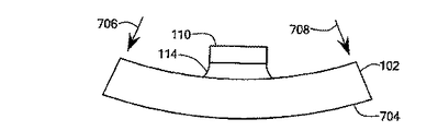
この発明は、ダイ取り付けの高温度に耐え、接着剤を使用せずにダイのためのハーメチック(気密)シールされた空間部を確保できる部品点数が少なく、低価格の回路パッケージを提供するものである。図1は、この発明の一つの実施例による模範的な回路パッケージ100を示す。分かりやすくするために、この回路パッケージは、蓋なしで示されている。前記回路パッケージ100には、フランジ102、フレーム104及び二つのリード106,108が含まれている。フレーム104は、二つのリード106,108をフランジ102に対し、そして互いに電気絶縁している。ダイ110は、共融合金はんだ付け部114などによりダイ取り付け領域112に取り付けられている。分かりやすくするために、図1では、一つのダイのみが示されているが、一般的には、二つ又はそれ以上のダイがダイ取り付け領域112に装着されるようになっている。
[Detailed Description of the Invention]
The present invention provides a low-cost circuit package with a low number of parts that can withstand the high temperature of die attachment and can secure a hermetic (airtight) sealed space for the die without using an adhesive. is there. FIG. 1 illustrates an
共融合金はんだ付け部114は、ダイ110をフランジ102へ電気的に接続している。共融合金はんだ付け部114は、また、ダイ110からフランジ102へ熱を逃がす。実用においては、フランジ102は、溝孔116,118に通されるボルト類(図示せず)によりヒートシンク(図示せず)に取り付けられるようになっているのが一般的ではある。ダイ110は、ワイヤ120,122などによりリード106,108に電気的に接続する。これらのワイヤ120,122は、リード106,108に超音波接合されていることが好ましい。一つのダイ110と二つのリード106,108が図示されているが、これら以上のダイ及び/又はリードも使用可能である。図2は、蓋200が施蓋された後の回路パッケージを示し、これについては、詳しく後記する。
A fusion
回路パッケージ100は、いくつかの特徴と構成を用いて前記ダイを前記空間キャビティ内にハーメッチクシールし、高温度に耐えるようにしている。前記したように、この組合せにより、前記回路パッケージ100の導電性、熱伝導性及び機械的一体性の度合いを高めているものでもある。以下の記述は、回路パッケージ100の製造のためのプロセスの全体像から始まるものである。ついで、フランジ102とその製造についての詳しい記述に移る。これに続いて、リード106,108、フレーム104に使用の液晶ポリマーの組成、蓋200そして回路パッケージ100の製造プロセスの詳細な説明に入ることとする。
[製造の全体像]
この発明による回路パッケージ100は、在来の回路パッケージ同様に帯状体又はリールに巻かれて製造されることが好ましい。図3は、リードフレーム302,304のようなリードフレームの帯状体300を示す。各リードフレームには、306,308で示されている二つのリードが含まれている。一つの実施例に於いては、リードフレーム帯状体300が打ち抜き又はエッチングされたとき、複数の孔がリード306,308に貫通される。これらの孔の例が310で示されている。これらの孔310は、詳しく後記するように、フレームをリード306,308にロックするために使用される。
[Overview of manufacturing]
The
リードフレーム帯状体300が作られた後、フレームが好ましくは射出成形でリードフレーム帯状体の各リードフレームに成形される。図4Aは、フレーム400のような複数のフレームが前記複数のリードフレームに成形された後のリードフレーム帯状体300Aを示す。図4Bは、一つの完成されたリードフレーム404を示す。複数のリードフレームは、一つ一つ個別に又は帯状体で又は巻かれて次々の製造作業者へ供給され、彼らによりダイが前記リードフレームに取り付けられる。
After the
[フランジ]
フランジ102は、基体となるもので、これに本回路パッケージの他のパーツ類が取り付けられる。さらに、フランジ102は、代表的には、ダイからヒートシンクへ熱を伝え、前記ダイの一つの端子をプリント基板に電気的に接続するものでもある。フランジ102は、好ましくは銅の含有率が高い合金(少なくとも約50%の銅)で作られ、導電性と熱伝導性に富み、ダイ取り付け温度におけるアニールに耐えるようになっている。この合金には、少なくとも一つの極微量の金属が含まれていることが好ましい。フランジ102は、少なくも約98%の銅と約0.05%から約1.5%のジルコニウムからなることが好ましいが、別の高い銅の含有率にしても差し支えない。フランジ102は、約99.9%の銅と約0.1%のジルコニウムからなることがさらに好ましい。フランジ102は、厚みが約2.54μm(約100マイクロインチ)のニッケルで電気めっきされて、拡散バリヤ層を形成し、約1.7μm(約65マイクロインチ)の金で電気めっきされて、ダイ110をフランジにはんだ付けするのを容易にする。
[Flange]
The
また別に、フランジ102は、少なくとも約99.5%の銅と約0.085%の銀からなるものでもよいが、別の高い銅の含有率にしても差し支えない。ジルコニウムは、銀より好ましいもので、これは、ジルコニウムを含有する合金は、銅の含有率が高く、したがって、熱伝導性と導電性が銀を含有する合金よりも良好であるからである。銅−ジルコニウム合金によりフランジの熱伝導性が従来技術の銅−タングステン及び銅−モリブデン−銅フランジよりもすぐれており、このようなフランジ又はこのようなフランジに取り付けられたダイを用いる回路パッケージは、従来技術のパッケージよりも大きな出力を出すことができるようになる。さらに加えて、銅−ジルコニウム合金は、銅含有率が高い大抵の合金よりもアニール温度が高く、ダイ取り付け温度までに加熱されても歪みが少ない。
Separately, the
上記したように、フレーム104は、好ましくは射出成形でフランジ102へ成形される。この成形の結果、前記フレームは、フランジ102にくっつくが、このくっつき方は、不完全であり、前記ダイのはんだ付けと動作の熱により破壊されてしまう。この問題を解決するために、フランジ102は、フレーム104と前記フランジとを機械的にインターロクする機械的特徴を含むことが好ましい。
As described above, the
この特徴は、図5Aに図示されているもので、この図は、図1を参照して述べた回路パッケージ100の一部の断面斜視図である。フランジ102には、フレーム保持構造部500が構成されていて、これは、フレーム104と前記フランジとを機械的に結合するために使用される。フレーム104をフランジ102に成形するとき、前記フレームの素材の一部が前記フレーム保持構造部500に流入し、硬化してキイ502が作られる。フレーム保持構造部500は、ある断面プロフィールを持ち、キイ50がこれに対する相補プロフィールをもつ。このようにして、硬化したキイ502は、フレーム保持構造部500にインターロックし、これによって、前記フレームと前記フランジとの間に接着剤を添加せずに、フレーム104がフランジ102から引き抜かれないようになる。
This feature is illustrated in FIG. 5A, which is a cross-sectional perspective view of a portion of the
フレーム保持構造部500は、少なくとも一つのアンダーカット部を含む。前記保持構造部500は、あり溝断面になっていて、アンダーカット部504,506を構成している。T、L又は円板に棒がついた形状のような他の断面形状でもよい。
The frame holding
図5Aに示されたフレーム保持構造部500は、フランジ102の隣接面に押し込まれるようになっているが、図5Bに示すように、前記隣接面から立ち上がるようになっていてもよい。別の形のフランジ102Aは、フレーム保持構造部500Aを構成し、これは、前記隣接面からしっかり立ち上がっている。フレーム104Aをフランジ102Aに成形するとき、前記フレームの素材の一部が前記フレーム保持構造部500Aのアンダーカット部504A,506Aにそってぐるりっと流れ込み、硬化する。この場合には、フレーム104A内側にキイ502Aが構成されることになる。
The
図5Aに戻ると、フレーム保持構造部500は、一連のプログレッシブ・スタンピング(一連の打ち抜き加工)によりフランジ102に形成される。図6A〜図6Cは、種々の加工段階におけるフレーム保持構造部500の断面を示す。図6Aは、フレーム保持構造部500が作られる前のフランジブランク102Bを示す。
Returning to FIG. 5A, the
図6Bは、前記フランジブランクに断面矩形の第1の溝600が作られたフランジブランク102Cを示す。この加工操作により溝600に壁602,604が作られる。溝600は、約0.508mm(約0.02インチ)の幅寸法(寸法A)になっていることが好ましく、約0.508mm(約0.02インチ)の深さ寸法(寸法B)になっていることが好ましい。
FIG. 6B shows a flange blank 102C in which a
図6Cは、第1の溝600に対し断面矩形の第2の溝606が作られた後のフランジ102を示す。この第2の加工操作により、壁602,604(図6B)を変形させ、この溝の頂部近辺を僅かにおしつぶす。変形した壁602A,604Aで図5Aを参照しての前記説明のようなアンダーカット部504,506が形成される。第2の溝606は、約1.27mm(約0.05インチ)の幅寸法(寸法D)になっていることが好ましく、約0.254mm(約0.01インチ)の深さ寸法(寸法C)になっていることが好ましい。このようにしてできた、あり溝形状のものは、約0.1778mm(約0.007インチ)の狭い寸法(寸法E)で、オーバーハング部分の寸法が約0.165mm(約0.0065インチ)(寸法F)になっている。オーバーハング部分(F)は、フレーム104に使用の液晶ポリマー(後記)に対し少なくとも約0.127mm(約0.005インチ)であることが好ましい。
FIG. 6C shows the
これらすべての寸法は、フランジ102のサイズ、素材及び温度、フレーム104のサイズ、素材及び温度、前記フランジとフレームの接合部分における所望の強度、コスト又は他の要素など、当業者の熟知しているものに応じて変えられるものである。
All these dimensions are familiar to those skilled in the art, such as
フランジ102には、また、機械的特徴が含まれていて、これは、フランジとヒートシンクとの間を熱が具合よく確実に伝わることようにする点である。ヒートシンク類は、一般的には、一方の面が機械的に研磨されて平坦になっている。回路パッケージとヒートシンクとの間の接合部の熱伝導を高めるために、前記回路パッケージをこの平坦な面に空隙無しにぴったり寄り添わせるようにしなければならない。
The
フレーム保持構造部500を作るために行われる打ち抜き加工(上記)でフランジ102の底部を変形させてしまい、これによって前記回路パッケージが前記ヒートシンクに対し平に寄り添えなくなる。このような変形を改善するために、フランジ102の底面を打ち抜き加工後にラップ盤で磨き上げることが好ましい。さらに、又は、別途に厚み寸法(5Aの寸法G)を好ましくは約3.175mm(約0.125インチ)厚くすることで、前記スタンプ(打ち抜き)加工による変形量を少なくし、フランジ102の底面をラップ磨き上げしなくてもすむようにできる。
The bottom part of the
ダイ110とフランジ102の熱伝導率CTEの相違で、前記ダイを前記フランジにはんだ付けするとき、前記フランジを変形させてしまう。図7A〜図7Dは、このような状況の略図である。図7Aは、平らな底面700をもつフランジ102Dと前記フランジに未だハンダ付けされていないダイ110を示す。はんだ材114Aは、未だ溶けていない。銅/ジルコニウムのフランジのCTEは、約17ppm/°Cであるが、シリコンのダイのCTEは、約2.8ppm/°Cである。ダイ110とフランジ102Dとが加熱されて該ダイを前記フランジにはんだ付けする際、前記ダイとフランジは、膨張する。
Due to the difference in thermal conductivity CTE between the die 110 and the
ついで、そして図7Bに示すように、ダイ110とフランジ102Dが冷えると、共融合金ハンダ114Bが直ちに硬化してしまうが、前記フランジとダイは、冷えながら収縮してゆく。共融合金はんだ114Bは、非常に硬く、ぐっと引き延ばされるものではない。したがって、フランジ102Dの上面702は、前記フランジよりもCTEがぐっと低いダイ110により拘束されてしまう。その結果、フランジ102Dの上面702は、その底面700よりも収縮度合いが小さく、該底面は、凹面形状になり、該フランジがヒートシンクに装着されると、間隙が残ってしまう。
Then, as shown in FIG. 7B, when the
はんだ付け後、フランジ102が凹面になる傾向に対抗するために、はんだ付けする前に前記フランジを僅かに凸面形状にしておく。図7Cは、ダイ110を該フランジにはんだ付けする前のフランジ102を示す。フランジ102の底面704は、凹面に張り出す寸法(寸法H)がはんだ付けにより導入される凹面になる度合いよりも大きな形状になる。一つの実施例においては、底面704は、前記フランジの長さにわたり少なくとも約0.00254mm(約0.0001インチ)だけ張り出している。別の実施例においては、底面704は、約0.0127mm(約0.0005インチ)から約0.0254mm(約0.0010インチ)の間の張り出しになっている。この寸法度合いは、使用されるはんだ付け技術フランジにはんだ付けされるダイの数、サイズと配置、前記フランジの長さ、幅及び厚さ、さらには前記フランジの構成などの種々の要因に応じて変わるものである。在来のフランジ類は、一般的には、厚みが約1.016mmまたは約1.575mm(約0.040又は0.062インチ)である。好ましくは約3.175mm(約0.125インチ)のフランジの厚さ(図5Aの寸法G)は、はんだ付けによる変形の量を減らすことができる。前記底面の張り出しは、成形加工により形成されることが好ましいが、サンドペーパー磨き、曲げ加工、鋳造又は鍜造のような別の加工でもよい。
After soldering, the flange is slightly convex before soldering to counter the tendency of the
図7Dは、前記ダイ110がフランジ102にはんだ付けされ、両者が冷えた後のフランジ102を示す。底面704は、好ましくは僅かに反った形になっている。フランジ102がヒートシンクに装着されると、ねじを前記フランジに取り付ける力(矢印706,708)で前記フランジがヒートシンクに対し平らにされ、フランジとヒートシンクの間の接合部の熱伝導性が良好になる。
FIG. 7D shows the
前記したように、フランジ102は、概ね平らなダイ取り付け領域112を含み、この領域にダイがはんだ付けされるか、エポキシ接着されるか又はその他の手段で取り付けられる。ダイ取り付け領域112は、25.4mm(インチ)当たり約0.0254mm(約0.001インチ)以下で平らになっていることが好ましく、さらに好ましくは25.4mm(インチ)当たり約0.0127mm(約0.0005インチ)以下で平らになっていて、ダイ110と前記ダイ取り付け領域とが具合よく共融合金はんだ接合されるようになっている。さらに、前記ダイ取り付け領域の粗さは、約1.6μm(約64マイクロインチ)以下であることが好ましく、これによってヒートシンクへ熱が良好に伝わるようになっている。エポキシのような接着剤を使用してファイ110をダイ取り付け領域112へ取り付ける場合には、ダイ取り付け領域の平坦度は、25.4mm(インチ)当たりやく0.127mm(約0.005インチ)内であることが好ましく、滑らかさは、約1.6μm(約64マイクロインチ)内になっている。
As described above, the
前記したように、フランジ102には、取り付け溝116,118が含まれている。また別に、フランジ102には、ねじがきってあるか、又は、ねじはきっていない複数の孔が含まれる。これらの場合、フランジ102は、これらの開口にボルト類や他のファスナー類によりヒートシンク又は他の代替品に取り付けられる。また別にフランジ102は、フランジ102をヒートシンク又は他の代替品にはんだ付けで取り付け溝をなくすこともできる。
As described above, the
[リード]
図1について前記したように、フレーム104は、好ましくは射出成形でフランジ102、リード1−6.108へ成形される。この成形工程の間、フレーム104は、リード106.108のまわりに成形されるのが好ましく、これらリードは、前記フレームの側壁を介して前記フレーム外側から空間キャビティ領域へ張り込む。この成形の結果、前記フレームは、リード106,108にくっつくが、このくっつきは、完全なものではなく、ダイのはんだ付けの熱及び動作によりこわれてしまう。この問題を解決するために、各リード106,108には、一つ又は複数のリード保持機構をもたせて前記リーソをフレーム104に固定するようにすることが好ましい。
[Lead]
As described above with respect to FIG. 1, the
リード保持機構の一つは、図8に示すように、各リードに少なくとも一つの孔310を貫通しておく。前記したように、これら孔310は、リードフレーム300(図3)を打ち抜いたり、エッチングしたりするときにリード106,108に形成するものである。フレーム104が前記リードに接触するラインにそって配置の複数の好ましくは矩形の孔310が各リード106,108に含まれていることが好ましい。成形工程の間、熱可塑性のフレーム素材が孔310へ流入し、硬化し、フレーム104内でリード106又は108を機械的にロックし、前記リードとフレームとの間に添加される接着剤の必要なしに前記フレームから前記リードが引き出されないようになる。図5Aに示すように、複数の孔310は、フレーム1−4により完全に覆われることが好ましい。
One of the lead holding mechanisms has at least one
リード106,108の導電性は、回路パッケージ100の全体のパフォーマンスに貢献するものである。リード106,108の導電性は、側面、即ち前記リードを通る電流の流れ方向に対しほぼ垂直な前記リードの断面領域に比例する。複数の孔310は、この断面領域(図8のB−B線部分参照)を狭くするから、前記孔の数、配置、サイズ及び形状を選択してリード106,108の効率的な導電性の損失を最低にすることができる。好ましくは、前記孔310は、前記リードの断面領域を最高約25%減らすことがきるが、構成されたリードの導電性が構造基準に合いさえすれば、この減少度をさらに低くできる。
The conductivity of the
矩形の孔310は、硬化してリード106,108をロックする熱可塑性フレーム素材の量を最も多量にする一方、前記リードの導電性の低下をなくすようにする。矩形の孔310の長い方の方向は、前記リード106,108を流れる電流の方向に平行になっていることが好ましい。フレーム104の側壁の厚さによっては、前記孔310を正方形にできる。
The
図8に示す別のリード保持構造では、フック状の又は曲げた(以下では、まとめて“フック状”という)エッジ800、畝部、凹部又は別の構造が空間キャビティ領域内にあるリード106,108の端部に又は端部近くに設けられている。この構造は、前記リードと同一平面上にはない。図5Aから分かるように、成形工程の間、フレームの熱可塑性素材の一部がこの構造の外側に面している部分において又は対し硬化し、これによってリード106がフレーム104から抜け出ないようにする機械的バリヤが作られる。フック状のエッジ800、畝部又は他の構造は、リードフレーム300(図3)が打ち抜き加工されるときにリード106,108に形成される。フック状エッジ800は、リード保持構造にとって好ましい実施例であるが、他の形状も使用できる。いくつかの許容できる形状のものの断面を図8Bに符号800A〜800Fで示す。
In another lead holding structure shown in FIG. 8, a
図1を参照して前記したように、リード106,108は、ダイ110を回路パッケージ又は均等物に電気的に接続するために用いられる。リード106,108は、銅の含有率が高い合金(銅が少なくとも50%)から作られて、良好な導電性をもち、フレーム104のCTEに合致するようになっている。銅の含有率が高いリードは、一般的にはニッケル42%、鉄55%の(合金42として広く知られている)従来のリード類よりもすぐれた導電性をもつ。さらに加えて、リード106,108は、拡散バリヤ層となる約2.54μm(約100マイクロインチ)のニッケル層と前記リードをワイヤボンドしたりはんだ付けしたりするのを容易にする約1.625μm(約65マイクロインチ)の金の層で電気めっきされるのが好ましい。
As described above with reference to FIG. 1, leads 106 and 108 are used to electrically connect die 110 to a circuit package or equivalent. The leads 106 and 108 are made of an alloy with a high copper content (copper is at least 50%), have good electrical conductivity, and conform to the CTE of the
リード106,108は、約2.1%〜約2.6%の鉄、約0.015%〜約0.15%の燐、約0.05%〜約0.2%の亜鉛及び残部が銅である合金で作られているものが好ましい。これら素材の割合は、これ以外のものでもよい。リード106,108は、約97.5%の銅、約2.35%の鉄、約0.3%の燐及び約0.12%の亜鉛のものから作られることがさらに好ましい。このような合金は、UNS識別C19400でOlin Corporationから入手できる。
リード106,108には、その他数多くの組成が適用できる。これら代替の一つとしては、約99.9%の銅と約0.1%のジルコニウムがある。このような合金は、UNS識別C15100でOlin Corporationから入手できる。これら素材の別の割合も差し支えない。例えば、約0.05%〜約0.15%のジルコニウムと残りが銅である合金もまた許容できる。
Many other compositions can be applied to the
リード106,108の別の組成には、約1%〜約2%の鉄、約0.01%〜約0.035%の燐、約0.3%〜約1.3%のコバルト、約0.1%〜約1%の錫及び残部が銅であるものが含まれる。この組成における好ましい銅の量は、97%である。このような合金は、UNS識別C19500でOlin Corporationから入手できる。
Another composition of the
リード106,108の別の組成には、約0.3%〜約1.2%の鉄、約0.1%〜約0.4%の燐、約0.01%〜約0.2%のマグネシウム、及び残部が銅であるものが含まれる。この代替組成における好ましい組成は、約0.6%の鉄、約0.2%の燐、約0.05%のマグネシウム、約99%の銅である。このような合金は、UNS識別C19700でOlin Corporationから入手できる。
Other compositions of
リード106,108の別の代替組成には、約1.7%〜約2.3%の錫、約0.1%〜約0.4%のニッケル、上限が約0.15%の燐及び残部が銅であるものが含まれる。このような合金は、UNS識別C50710で三菱電機株式会社から入手できる。
Another alternative composition for
リード106,108のさらに別の代替組成には、約0.05%〜約1.5%の鉄、約0.025%〜約0.045%の燐及び残部が銅であるものが含まれる。このような合金は、UNS識別C19210で神戸製鋼所から入手できる。
Yet another alternative composition for the
リード106,108のさらに別の代替組成には、約0.5%〜約0.15%の鉄、約0.5%〜約1.5%の錫、約0.01%〜約0.035%の燐および残部が銅であるものが含まれる。このような合金は、UNS識別C19520で三菱伸銅株式会社から入手できる。
Yet another alternative composition for the
リード106,108の別の代替組成には、約0.15%〜約0.4%のクロミウム、約0.01%〜約0.4%のチタン、約0.02%〜約0.07%のシリコン及び残部が銅であるものが含まれる。このような合金は、UNS識別C18070でWieland Werkeから入手できる。
Other alternative compositions for
リード106,108のさらに別の代替組成には、約0.8%のニッケル、約0.15%〜約0.35%のシリコン、約0.01%〜約0.05%の燐及び残部が銅であるものが含まれる。このような合金は、UNS識別C19010でSan Metal Corporationから入手できる。
Yet another alternative composition for
リード106,108の別の代替組成には、約2.0%〜約4.8%のニッケル、約0.2%〜約1.4%のシリコン、約0.05%〜約0.45%のマグネシウム及び残部が銅であるものが含まれる。この代替組成における好ましい組成は、約3.0%のニッケル、約0.65%のシリコン、約0.15%のマグネシウム、約96.2%の銅である。このような合金は、UNS識別C70250でOlin Corporationから入手できる。
Other alternative compositions for
リード106,108のさらに別の代替組成には、約0.3%〜約0.4%のクロミウム、約0.2%〜約0.3%の錫、約0.15%〜約0.25%の亜鉛及び残部が銅であるものが含まれる。このような合金は、UNS識別EFTEC−64Tで古河電気から入手できる。
Yet another alternative composition for
リード106,108の別の代替組成には、約2.7%〜約3.7%のニッケル、約0.2%〜約1.2%のシリコン、約0.1%〜約0.5%の亜鉛及び残部が銅であるものが含まれる。このような合金は、UNS識別KLF−25で神戸製鋼所から入手できる。
Other alternative compositions for the
リード106,108のさらに別の代替組成には、約1.9%〜約2.9%のニッケル、約0.2%〜約0.6%のシリコン、約0.1%〜約0.2%の燐及び残部が銅であるものが含まれる。このような合金は、UNS識別NF224で三菱電機株式会社から入手できる。
Yet another alternative composition for the
[フレーム]
図5Aに関連して上記したように、フレーム104は、熱可塑性素材の射出成形で成形されフランジ102とリード106,108に一体成形される。フランジ102の素材には、好ましくは、液晶ポリマー(LCP)が含まれ、これは、ダイ取り付け温度(AuSnはんだ付けの温度280〜330℃又はAuSiはんだ付けの温度390〜420℃)に耐えることができる。従来のLCP類は、約300℃〜約330℃の範囲の温度で溶けてしまう。フレーム104には、その溶融温度を上げ、熱膨張係数(CTE)を調節し、湿気の浸透度を減らすベース樹脂とコンパウンド類が含まれている。実用的には、前記樹脂類とコンパウンド類を含むフレーム104の素材をここでは“熱可塑性コンパウンド”又は“フレーム材(マテリアル)”という。
[flame]
As described above with reference to FIG. 5A, the
許容できる樹脂の例は、p−ヒドロキシ安息香酸、ビスフェノ−ル及びフタール酸からなるものである。他の許容される配合処方は、p−ヒドロキシ安息香酸(HBA)と6−ヒドロキシ−2−ナフトエ酸(HNA)の共重合体を含む。他の許容される配合処方はHBA、4−4‐ビフェノール(BP)およびテレフタール酸(TA)のテラ(tera)ポリマーを含む。 Examples of acceptable resins are those consisting of p-hydroxybenzoic acid, bisphenol and phthalic acid. Another acceptable formulation includes a copolymer of p-hydroxybenzoic acid (HBA) and 6-hydroxy-2-naphthoic acid (HNA). Other acceptable blend formulations include tera polymers of HBA, 4-4-biphenol (BP) and terephthalic acid (TA).
図9は、フレーム104の断面図の概略図であり、熱可塑性材中の化合物のいくつかを示す。充填材粒子は好ましくはLCPへ添加され、そのCTEをリード106と108のCTE(約17 ppm/℃)に、より近接して調和するように変成し、フレーム102中の熱可塑性材の異方性が阻害される。フレーム材のCTEは好ましくはリード106と108のCTEの約60%内にあるように調節される。無機材900の球状体、たとえばタルクであり、好ましくは2〜3ミクロン径であり、LCPに添加され、その濃度は約30%〜約40%の範囲である。このような複合材は約7ppm/℃〜22ppm/℃のCTEを有する。
FIG. 9 is a schematic diagram of a cross-sectional view of the
グラファイトは、好ましくLCPへ添加され、湿気の進入を減らす。このグラファイトは好ましく、一般的に平板のグラファイト・フレーク904(図9に、真横から見た方向で(エッジオン)示される)形状であるが、しかし他の形状のグラファイト、例えば、球形、塊状もまた許容される。加えて、グラファイト・フレーク904は射出等の際にある程度撓むが、有意にはその有効性が減じることはない。用語“一般的に平面状グラファイト・フレーク”は変形したフレークも含むものである。
Graphite is preferably added to the LCP to reduce moisture ingress. This graphite is preferred and is generally in the form of a flat graphite flake 904 (shown in FIG. 9 as viewed from the side (edge-on)), but other shapes of graphite, such as spheres and lumps, are also possible. Permissible. In addition, the
グラファイト・フレーク904は、好ましくは層構造をとり、好ましくはフレーム104の外表面に概略平行であり、かくして湿気侵入の通路を曲がりくねったものとしている。前記層構造が外表面に平行でなくとも、グラファイトの存在で湿気の進入が抑制される。グラファイト・フレーク904はまたLCPのCTEを調整して、リード106と108の銅合金に、より近接してマッチさせる。フレーム材は、約10%と約70%の間のグラファイト・フレークを含み、好ましくは約40%と約50%の間である。
The
グラファイト・フレークの代替物としては、ガラスファイバー1202がLCPへ添加されることができ、剛性が増し、得られる熱可塑性材のCTEが調整される。この態様では、フレーム材は好ましくは約30%と約50%の間の割合のガラスファイバーを含む。 As an alternative to graphite flakes, glass fibers 1202 can be added to the LCP to increase rigidity and adjust the CTE of the resulting thermoplastic. In this embodiment, the frame material preferably includes a proportion of between about 30% and about 50% glass fiber.
グラファイト・フレークの他の代替として、または追加としては、他の材料をLCPへ添加することができ、それは例えば、鉄粉基材の吸収剤、分子篩のろ過材(ゼオライト)および酸化カルシウム(CaO)である。適当なゼオライトは、サッド−化学から入手できる。 As another alternative or in addition to graphite flakes, other materials can be added to the LCP, such as iron powder based absorbents, molecular sieve filter media (zeolites) and calcium oxide (CaO). It is. Suitable zeolites are available from Sad-Chem.
フレーム剤は、射出成形前に、好ましくは予備乾燥されて、好ましくは約0.008%未満の水分とされる。さらに、射出成形時間は短い時間で行なうものとして、好ましくは約0.2秒未満である。ワンショットの射出のサイズは、小さいものとし、好ましくは約2グラム未満として、熱可塑性材の射出成形機のバレル内に滞留する時間を最小限とする。射出成形時のゲートは、好ましくは熱可塑性材の流れを制限し、それにより熱可塑性材におけるせん断力を増大させて、ポリマー鎖とグラファイト・フレーク904を配向させる。熱可塑性材は、好ましくはフレーム104の角でまたはリード106と108の間で射出される。得られるフレームにおける残留応力の量を減らすために約250°Fという最低の金型温度が、好ましくは成形操作の間維持される。
The frame agent is preferably pre-dried prior to injection molding, and preferably has a moisture content of less than about 0.008%. Further, the injection molding time is preferably less than about 0.2 seconds as it is performed in a short time. The size of the one-shot injection should be small and preferably less than about 2 grams to minimize the residence time in the barrel of the thermoplastic injection molding machine. The gate during injection molding preferably restricts the flow of the thermoplastic material, thereby increasing the shear force in the thermoplastic material and orienting the polymer chains and
湿気防止フィルムを好ましくはフレーム104の外表面に貼付して、湿気の侵入をさらに減らすことができる。代替としては、フィルムはフレーム104の内側に貼付され得る。許容される材料はアミン基材のエポキシ樹脂を含み、PPGインダストリーから商品名 Bairocadeで入手できる ポリマー/Alフィルムおよびポリマー/セラミック・フィルムである。
A moisture-preventing film is preferably applied to the outer surface of the
封止
フレーム保持構造部500(図5A)とリード保持構造部800(図8A)は良好な機械的な接合部を構成し、湿気と大気ガスの進入を抑制する。さらに、フレーム104は、好ましくは添加剤と内側または外側にフィルムを貼付されて、この侵入を減少させる。さらに進入を減少させるには、図10に示すように、封止1000と1002を、好ましくはフレーム104の縁に沿ってフレーム104の内部に施し、そこではフレームはリード106,108と接し、またフレームはフランジ102に接する。図11Aの断面図に示されるように、封止1002は、フランジ102とフレーム104の間からの浸入の防止と、フレーム104とリード108の間の浸入防止に効果的である。代替としては、図11Bに示すように、二つの封止、1002Aと1002Bを一つの封止1002に代って使用することができる。
The sealing frame holding structure 500 (FIG. 5A) and the lead holding structure 800 (FIG. 8A) constitute a good mechanical joint and suppress the ingress of moisture and atmospheric gas. Further, the
フレーム材へ封止材が良好に接着するのを促進するには、好ましくは封止材の適用の前に洗浄をすることである。プラズマ洗浄は、当業者に周知であり、酸素が主たる媒体であるが、許容され得る結果をもたらす。代替として、フレーム材は、溶剤またはエッチングで洗浄され得る。内径0.203mm(0.008インチ)の針が封止1000の材料を施与するのに使用され、そして内径0.254mm(0.010インチ)のID針が、封止1002の材料を施与するのに使用される。所望のビードの大きさに応じて他のサイズの針が使用され得る。封止材中の空気泡を最小にするために、容積式のオーガーポンプが封止材を針に注入するのに使用される。
To promote good adhesion of the encapsulant to the frame material, it is preferable to wash before applying the encapsulant. Plasma cleaning is well known to those skilled in the art and oxygen is the primary medium, but with acceptable results. Alternatively, the frame material can be cleaned with a solvent or etch. An inner diameter 0.203 mm (0.008 inch) needle is used to apply the
封止材は好ましくはせん断速度約0.95/秒における約58Pa.sと約128Pa.sの間の粘度を有し、そしてせん断速度約9.5/秒における約12Pa.sと約30Pa.sの間の粘度を有している。図12は、グラフ1200を含み、それは粘度とせん断速度の間の関係を示す。低い粘度が高せん断速度では好ましく、それにより材料は迅速に施与され得る。しかし、高粘度が低速のせん断速度では好ましく、それにより一旦材料が施与されても、その材料は流れないこととなる。
The encapsulant is preferably about 58 Pa.s at a shear rate of about 0.95 / sec. s and about 128 Pa.s. s and a viscosity of about 12 Pa. at a shear rate of about 9.5 / sec. s and about 30 Pa.s. having a viscosity between s. FIG. 12 includes a
材料は、好ましくは約3Pa.sと約7.4Pa.sの間のケーソン(cason)粘度を有する。材料のチクソトロピー性指数は好ましくは約3.5と約4.6の間にある。 The material is preferably about 3 Pa.s. s and about 7.4 Pa.s. with cason viscosity between s. The thixotropic index of the material is preferably between about 3.5 and about 4.6.
封止1000と1002の適当な材料は、エポキシ樹脂、シリコーン樹脂および相似被覆(conformal coating)を含む。適当な封止材は、約40%と約60%の間の溶剤(例えば、酢酸(2−ブチル)エステル)と、約40%と約60%の間のエポキシ樹脂またはシリコーン樹脂を含む。エポキシ樹脂は、たとえばビスフェノール−A型または脂環式エポキシ樹脂である適当な硬化剤にはアミン系硬化剤が含まれる。代替として、封止材はコックソン電気から得られるパラリレンD(Paralyne D)またはパーリレンHT(Parylene HT)とすることができる。
Suitable materials for
蓋(Lid)
蓋200は、ダイ110がフランジ102に付けられてリード106,108に電気的に接続された後に、フレーム104に取り付けられる。適当な蓋200は、図13Aと13Bに示される。蓋200は、好ましくはフレーム104に超音波・溶接され、それは約50kHzと約60kHzの間の振動数と約100ミクロン未満(より好ましくは60ミクロン未満)の振幅の溶接信号を使用する。代替としては、蓋200はレーザー溶接または熱溶接でフレーム104に溶接される。
Lid
The
通常の超音波プラスチック溶接技術は、蓋で回路パッケージをシールするのに使用されないのは、このような従来の技術が低い周波数の溶接を利用するからであり、これによる高い振幅が回路パッケージに実装された配線・結線を損傷することがあるのである。本発明の高い溶接周波数は低い振幅となり、その結果配線・結線を損傷することがない。通常、蓋は、回路パッケージにエポキシ接着剤で接着される。有利には、蓋の回路パッケージへの接合は、エポキシ樹脂の硬化時間(約2時間)よりも短い時間(約250 ミリセカンド)の超音波溶接でなされる。 The usual ultrasonic plastic welding technique is not used to seal the circuit package with the lid because such conventional techniques utilize low frequency welding and the resulting high amplitude is mounted on the circuit package. It may damage the wiring and connection. The high welding frequency of the present invention has a low amplitude, and as a result, does not damage the wiring / connection. Usually, the lid is adhered to the circuit package with an epoxy adhesive. Advantageously, the lid is bonded to the circuit package by ultrasonic welding for a time (about 250 milliseconds) that is shorter than the curing time of the epoxy resin (about 2 hours).
蓋200とフレーム104の間には好ましくは緩衝性の嵌め合いが存在し、そうして蓋とフレームの両方の部分が超音波溶接の間互いに溶解・溶融する。図13Bの断面図に示されるように、蓋200は好ましくは、フレーム104と溶解・溶融するリップ1300を含む。蓋200は、好ましくは上述のようにフレーム104と同じ材料からなる。さらに、フレーム104に関して上で説明したように湿気防止フィルムが好ましくは蓋200に貼られる。
There is preferably a cushioning fit between the
製造の詳細
回路パッケージ100のフランジ102、フレーム104、リード106,108および蓋200およびこれらの部品の製造に使用される材料、方法を含み、その詳細は上記で説明される。図14は、方法を説明する単純化したフローチャートを例示し、それにより回路パッケージ100が製造されて使用され得る。
Manufacturing Details Includes the
1400では、第1の高含量銅の合金がリード106,108のために製造される。1402では、リードフレームが1400で製造された第1の高含量銅合金から製作される。1404では孔310が穿孔され、エッチングまたはそうでない方法でリードフレームに施され、リード保持構造の一つが製作される。1406では、リード106、108の端部がカールされ、折り曲げられ、打ち抜かれ、またはリードフレーム300にエッチングされ、他のリード保持構造800が作成される。
At 1400, a first high content copper alloy is produced for the leads 106,108. At 1402, a lead frame is fabricated from a first high content copper alloy produced at 1400. At 1404, holes 310 are drilled and etched or otherwise applied to the lead frame to produce one of the lead holding structures. At 1406, the ends of the
1408では、第2の高含量銅合金がフランジ102のために製造される。1410では、フランジ102が1408で製造された第2の高含量銅合金により製作される。1412では、フレーム保持構造500が、連続スタンプ方法によりフランジ102に造り出される。任意に、1414で、フランジ102の底部が折り畳まれる。1416ではフランジ102の底部が凸状とされる。
At 1408, a second high content copper alloy is produced for the
1418では、グラファイト・フレーク、タルクおよび/またはガラスファイバーが液晶ポリマーに添加されてフレーム材が製造される。1420では、フレーム材が乾燥される。1422では、フレーム104は、フランジ102とリード1−6、108へ成形される.
At 1418, graphite flakes, talc and / or glass fibers are added to the liquid crystal polymer to produce a frame material. At 1420, the frame material is dried. At 1422, the
1424では、フレーム104とフランジ102の内部、すなわち、空気キャビティー領域が、洗浄される。1426では、封止材が施与されて、フレーム104とフランジ102の間およびフレームとリード106、108の間の境界をシールする。
At 1424, the interior of the
1428では、ダイ110がフランジ102に取り付けられる。1430では、ダイ110は、リード106、108に超音波により配線結合される。1432では、蓋200はフレーム104に超音波溶着される。
At 1428, die 110 is attached to
本発明は好ましい態様をもとに説明されてきたが、当業者ならば、変形が可能であるが、依然として添付の請求の範囲に記載のように本発明の範囲と精神の範囲内にあることを理解する。たとえば、低いパワーダイは、半田付けされるよりも、むしろフランジにエポキシまたはそれではない接着剤で接着され得る。さらに、当業者に良く知られているように、合金は典型的には少量の不純物を含み、そのためここに述べられる組成は必ずしも合計で100%にならない。 While the invention has been described in terms of a preferred embodiment, those skilled in the art can make modifications but still fall within the scope and spirit of the invention as set forth in the appended claims. To understand the. For example, a low power die can be glued to the flange with epoxy or non-solder rather than being soldered. Further, as is well known to those skilled in the art, alloys typically contain small amounts of impurities, so that the compositions described herein do not necessarily add up to 100%.
フレーム保持構造500とフランジ底部の凸状体Hは高含量銅フランジ102の関係で説明されているが、これらの創作はまた通常のフランジや他の材料からのフランジにも適用される。リード保持構造310、800およびそれらの各自の大体は高含量銅のリードの関係で説明されているが、これらの創作もまた通常のリードと他の材料からなるリードにも適用される。フレーム材は回路パッケージ100の関係で説明されてきたが、この材料は、有利には、他の関係、例えば高温に耐える材料を必要とするようなものとの関係で使用され得る。フレーム材の他の応用の例は、印刷回路板(PCBs)における高温積層や電子部品、ケーブル、PCBs等のソケットを含む。
Although the
100 回路パッケージ
102 フランジ
104 フレーム
106 リード
108 リード
110 ダイ
112 ダイ取り付け領域
114 共融合金半田
116 スロット
118 スロット
120 配線
122 配線
DESCRIPTION OF
Claims (23)
該フレーム構造体は液晶ポリマー材料からなり、表面を有し、かつ、The frame structure is made of a liquid crystal polymer material, has a surface, and
該液晶ポリマー材料は複数の平面状グラファイト・フレークを含有すると共に、The liquid crystal polymer material contains a plurality of planar graphite flakes,
該グラファイト・フレークは前記表面に平行に層構造として存在し、かつ、該グラファイト・フレークの層により外部からの湿気の侵入を防止する曲がりくねった通路が形成されているThe graphite flakes exist as a layer structure parallel to the surface, and a tortuous passage that prevents moisture from entering from the outside is formed by the graphite flake layer.
ことを特徴とする集積回路パッケージ用フレーム構造体。A frame structure for an integrated circuit package.
該フレーム構造体は液晶ポリマー材料と複数の平面状グラファイト・フレークとを含有する組成物からなり、表面を有し、かつ、The frame structure is composed of a composition containing a liquid crystal polymer material and a plurality of planar graphite flakes, has a surface, and
前記グラファイト・フレークは前記表面に平行に層構造として存在し、かつ、該グラファイト・フレークの層により外部からの湿気の侵入を防止する曲がりくねった通路が形成されているThe graphite flakes exist in a layer structure parallel to the surface, and a tortuous passage that prevents moisture from entering from outside is formed by the graphite flake layer.
ことを特徴とする集積回路パッケージ用フレーム構造体。A frame structure for an integrated circuit package.
液晶ポリマー材料と複数の平面状グラファイト・フレークとを含有してなる組成物を供給する工程と、Supplying a composition comprising a liquid crystal polymer material and a plurality of planar graphite flakes;
該組成物を型に射出成型することにより、前記グラファイト・フレークがフレーム構造体の表面に平行に層構造として存在し、かつ、該グラファイト・フレークの層により外部からの湿気の侵入を防止する曲がりくねった通路を形成する工程と、By injecting the composition into a mold, the graphite flakes exist in a layer structure parallel to the surface of the frame structure, and the graphite flake layer is bent to prevent moisture from entering from the outside. Forming a closed passage;
を有してなることを特徴とする集積回路パッケージ用フレーム構造体の製造方法。A method for manufacturing a frame structure for an integrated circuit package, comprising:
Applications Claiming Priority (2)
| Application Number | Priority Date | Filing Date | Title |
|---|---|---|---|
| US44347003P | 2003-01-29 | 2003-01-29 | |
| US60/443,470 | 2003-01-29 |
Related Parent Applications (1)
| Application Number | Title | Priority Date | Filing Date |
|---|---|---|---|
| JP2006503126A Division JP4780718B2 (en) | 2003-01-29 | 2004-01-29 | Package for integrated circuit die |
Publications (2)
| Publication Number | Publication Date |
|---|---|
| JP2010239144A JP2010239144A (en) | 2010-10-21 |
| JP5554635B2 true JP5554635B2 (en) | 2014-07-23 |
Family
ID=32825334
Family Applications (3)
| Application Number | Title | Priority Date | Filing Date |
|---|---|---|---|
| JP2006503126A Expired - Lifetime JP4780718B2 (en) | 2003-01-29 | 2004-01-29 | Package for integrated circuit die |
| JP2010129720A Expired - Lifetime JP5554635B2 (en) | 2003-01-29 | 2010-06-07 | Integrated circuit package frame structure and manufacturing method thereof |
| JP2010129717A Expired - Lifetime JP5554634B2 (en) | 2003-01-29 | 2010-06-07 | Manufacturing method of flange for mounting semiconductor die |
Family Applications Before (1)
| Application Number | Title | Priority Date | Filing Date |
|---|---|---|---|
| JP2006503126A Expired - Lifetime JP4780718B2 (en) | 2003-01-29 | 2004-01-29 | Package for integrated circuit die |
Family Applications After (1)
| Application Number | Title | Priority Date | Filing Date |
|---|---|---|---|
| JP2010129717A Expired - Lifetime JP5554634B2 (en) | 2003-01-29 | 2010-06-07 | Manufacturing method of flange for mounting semiconductor die |
Country Status (8)
| Country | Link |
|---|---|
| US (6) | US6867367B2 (en) |
| EP (1) | EP1627419A4 (en) |
| JP (3) | JP4780718B2 (en) |
| KR (1) | KR101025079B1 (en) |
| CN (4) | CN101436572B (en) |
| CA (1) | CA2514515C (en) |
| SG (4) | SG157957A1 (en) |
| WO (1) | WO2004068558A2 (en) |
Families Citing this family (95)
| Publication number | Priority date | Publication date | Assignee | Title |
|---|---|---|---|---|
| EP1548905A4 (en) * | 2002-09-30 | 2006-08-09 | Sanyo Electric Co | Light emitting element |
| US7298046B2 (en) * | 2003-01-10 | 2007-11-20 | Kyocera America, Inc. | Semiconductor package having non-ceramic based window frame |
| SG157957A1 (en) * | 2003-01-29 | 2010-01-29 | Interplex Qlp Inc | Package for integrated circuit die |
| WO2004090938A2 (en) * | 2003-04-02 | 2004-10-21 | Honeywell International Inc. | Thermal interconnect and interface systems, methods of production and uses thereof |
| WO2004109795A2 (en) * | 2003-06-06 | 2004-12-16 | Honeywell International Inc. | Thermal interconnect system and method of production thereof |
| JP2005129735A (en) * | 2003-10-23 | 2005-05-19 | Fujitsu Media Device Kk | Electronic component |
| US7259460B1 (en) * | 2004-06-18 | 2007-08-21 | National Semiconductor Corporation | Wire bonding on thinned portions of a lead-frame configured for use in a micro-array integrated circuit package |
| US20060145317A1 (en) * | 2004-12-31 | 2006-07-06 | Brennan John M | Leadframe designs for plastic cavity transistor packages |
| DE102005006281B4 (en) * | 2005-02-10 | 2014-07-17 | Infineon Technologies Ag | High frequency power device with gold coatings and method of making the same |
| US20100201003A1 (en) * | 2005-03-02 | 2010-08-12 | Dane Thompson | Packaging Systems Incorporating Thin Film Liquid Crystal Polymer (LCP) and Methods of Manufacture |
| JP4797621B2 (en) * | 2005-06-30 | 2011-10-19 | 日亜化学工業株式会社 | Semiconductor device and manufacturing method thereof |
| US7280181B2 (en) * | 2005-06-30 | 2007-10-09 | Intel Corporation | Liquid crystal polymer optical filter carrier |
| US7848698B2 (en) | 2005-07-22 | 2010-12-07 | Appareo Systems Llc | Flight training and synthetic flight simulation system and method |
| US8944822B2 (en) * | 2005-07-22 | 2015-02-03 | Appareo Systems, Llc | Synchronized video and synthetic visualization system and method |
| US7336491B2 (en) * | 2005-09-06 | 2008-02-26 | Lear Corporation | Heat sink |
| US8120153B1 (en) * | 2005-09-16 | 2012-02-21 | University Of Central Florida Research Foundation, Inc. | High-temperature, wirebondless, injection-molded, ultra-compact hybrid power module |
| US7429790B2 (en) * | 2005-10-24 | 2008-09-30 | Freescale Semiconductor, Inc. | Semiconductor structure and method of manufacture |
| US7446411B2 (en) * | 2005-10-24 | 2008-11-04 | Freescale Semiconductor, Inc. | Semiconductor structure and method of assembly |
| US20070175660A1 (en) * | 2006-01-27 | 2007-08-02 | Yeung Betty H | Warpage-reducing packaging design |
| US9202318B2 (en) | 2006-09-25 | 2015-12-01 | Appareo Systems, Llc | Ground fleet operations quality management system |
| US8116922B2 (en) * | 2006-09-25 | 2012-02-14 | Appareo Systems, Llc | Method for resolving ground level errors in simulations |
| US7616449B2 (en) * | 2006-09-25 | 2009-11-10 | Appareo Systems, Llc | Crash-hardened memory device and method of creating the same |
| US9172481B2 (en) | 2012-07-20 | 2015-10-27 | Appareo Systems, Llc | Automatic multi-generational data caching and recovery |
| US9047717B2 (en) | 2006-09-25 | 2015-06-02 | Appareo Systems, Llc | Fleet operations quality management system and automatic multi-generational data caching and recovery |
| US8565943B2 (en) * | 2006-09-25 | 2013-10-22 | Appereo Systems, LLC | Fleet operations quality management system |
| US7679185B2 (en) * | 2006-11-09 | 2010-03-16 | Interplex Qlp, Inc. | Microcircuit package having ductile layer |
| CN101578711A (en) * | 2006-11-09 | 2009-11-11 | 跃进封装公司 | Leg reflective package |
| US20080150064A1 (en) * | 2006-12-12 | 2008-06-26 | Zimmerman Michael A | Plastic electronic component package |
| US7608482B1 (en) * | 2006-12-21 | 2009-10-27 | National Semiconductor Corporation | Integrated circuit package with molded insulation |
| US7874846B2 (en) * | 2007-06-22 | 2011-01-25 | Seagate Technology Llc | Hermetically sealed liquid crystal polymer interconnect |
| US7715211B2 (en) * | 2007-07-17 | 2010-05-11 | Tellabs Operations, Inc. | Configurable printed circuit board |
| US8014167B2 (en) * | 2007-09-07 | 2011-09-06 | Seagate Technology Llc | Liquid crystal material sealed housing |
| US20090309199A1 (en) * | 2008-06-12 | 2009-12-17 | Keith Richard Barkley | Chip package for semiconductor devices |
| KR100951888B1 (en) * | 2008-06-18 | 2010-04-12 | 주식회사 다윈전자 | Semiconductor Package Structure |
| US20100012354A1 (en) * | 2008-07-14 | 2010-01-21 | Logan Brook Hedin | Thermally conductive polymer based printed circuit board |
| US20100092790A1 (en) * | 2008-10-14 | 2010-04-15 | Gm Global Technology Operations, Inc. | Molded or extruded combinations of light metal alloys and high-temperature polymers |
| US8288845B2 (en) * | 2008-11-14 | 2012-10-16 | Triquint Semiconductor, Inc. | Package including proximately-positioned lead frame |
| US8124447B2 (en) * | 2009-04-10 | 2012-02-28 | Advanced Semiconductor Engineering, Inc. | Manufacturing method of advanced quad flat non-leaded package |
| US8110445B2 (en) * | 2009-05-06 | 2012-02-07 | Infineon Technologies Ag | High power ceramic on copper package |
| CN102482428B (en) * | 2009-08-20 | 2014-12-31 | Iqlp有限责任公司 | Ultra high-remperature plastic package and method of manufacture |
| TWI468446B (en) * | 2009-08-21 | 2015-01-11 | Iqlp Llc | Ultra high-temperature plastic package and method of manufacture |
| US8853843B2 (en) | 2009-10-14 | 2014-10-07 | Stmicroelectronics, Inc. | Modular low stress package technology |
| US8597984B2 (en) | 2009-10-14 | 2013-12-03 | Stmicroelectronics, Inc. | Modular low stress package technology |
| US8639373B2 (en) * | 2009-10-14 | 2014-01-28 | Stmicroelectronics, Inc. | Modular low stress package technology |
| US8314487B2 (en) * | 2009-12-18 | 2012-11-20 | Infineon Technologies Ag | Flange for semiconductor die |
| US9728868B1 (en) * | 2010-05-05 | 2017-08-08 | Cree Fayetteville, Inc. | Apparatus having self healing liquid phase power connects and method thereof |
| CN102271459B (en) | 2010-06-03 | 2014-09-24 | 矢崎总业株式会社 | Wiring substrate and manufacturing method thereof |
| WO2011155317A1 (en) * | 2010-06-09 | 2011-12-15 | シャープ株式会社 | Heat dissipation structure for electronic device |
| JP5679561B2 (en) * | 2011-02-23 | 2015-03-04 | 矢崎総業株式会社 | Plastic molded product |
| DE102011004694A1 (en) * | 2011-02-24 | 2012-08-30 | Robert Bosch Gmbh | Circuit device for transmission control unit used in motor car, has absorber containing hydrophobic bulk material, that is sealed in inner space for absorbing penetrated oil from outside |
| CN102756456B (en) * | 2011-04-27 | 2015-04-22 | 无锡华润安盛科技有限公司 | Die for pre-plastic package of a lead frame and encapsulation structure |
| CA2837730C (en) * | 2011-06-27 | 2019-05-07 | Eaton Corporation | Grounded circuit breaker panel electrical module and method for grounding same |
| US8916421B2 (en) * | 2011-08-31 | 2014-12-23 | Freescale Semiconductor, Inc. | Semiconductor device packaging having pre-encapsulation through via formation using lead frames with attached signal conduits |
| US9142502B2 (en) | 2011-08-31 | 2015-09-22 | Zhiwei Gong | Semiconductor device packaging having pre-encapsulation through via formation using drop-in signal conduits |
| BR112014007550A2 (en) | 2011-09-30 | 2017-04-11 | Saint Gobain Performance Plastics Corp | fusion-processed fluoropolymer article and method for processing fusion-fluoropolymers |
| US8597983B2 (en) | 2011-11-18 | 2013-12-03 | Freescale Semiconductor, Inc. | Semiconductor device packaging having substrate with pre-encapsulation through via formation |
| US8698291B2 (en) | 2011-12-15 | 2014-04-15 | Freescale Semiconductor, Inc. | Packaged leadless semiconductor device |
| US8824151B2 (en) * | 2012-02-13 | 2014-09-02 | Ford Global Technologies, Llc | Mounting system for an electronic control module housing in a vehicle |
| JP5636096B2 (en) * | 2012-03-27 | 2014-12-03 | 積水化学工業株式会社 | Resin composite material |
| US8906747B2 (en) | 2012-05-23 | 2014-12-09 | Freescale Semiconductor, Inc. | Cavity-type semiconductor package and method of packaging same |
| US8803302B2 (en) | 2012-05-31 | 2014-08-12 | Freescale Semiconductor, Inc. | System, method and apparatus for leadless surface mounted semiconductor package |
| DE102012022960B4 (en) * | 2012-11-23 | 2021-12-30 | Schott Ag | Housing component, in particular for an electronics housing, and method for producing a housing component |
| EP2854162B1 (en) | 2013-09-26 | 2019-11-27 | Ampleon Netherlands B.V. | Semiconductor device leadframe |
| EP2854161B1 (en) * | 2013-09-26 | 2019-12-04 | Ampleon Netherlands B.V. | Semiconductor device leadframe |
| CN104797075B (en) * | 2014-01-17 | 2019-02-26 | 中兴通讯股份有限公司 | Arch PCB and its design method |
| JP6305778B2 (en) * | 2014-01-30 | 2018-04-04 | ローム株式会社 | Power module and manufacturing method thereof |
| EP3118895B1 (en) * | 2014-03-13 | 2020-04-01 | Kyocera Corporation | Package for housing an electronic component and electronic device including the package |
| JP6375584B2 (en) * | 2014-03-31 | 2018-08-22 | 住友電工デバイス・イノベーション株式会社 | Electronic component mounting package |
| EP3146560A4 (en) * | 2014-05-23 | 2018-04-18 | Materion Corporation | Air cavity package |
| CN103978348A (en) * | 2014-05-28 | 2014-08-13 | 福清泳贸塑胶有限公司 | Processing method and structure of left base plate of computer displayer back plate |
| CN105990271B (en) * | 2015-02-26 | 2020-06-05 | 恩智浦美国有限公司 | IC package with non-horizontal die pad and corresponding lead frame |
| JP6397127B2 (en) * | 2015-05-20 | 2018-09-26 | 京セラ株式会社 | Semiconductor element package, semiconductor device, and mounting structure |
| CN106486426A (en) * | 2015-08-26 | 2017-03-08 | 比亚迪股份有限公司 | Metal-ceramic plate for welding chip and the thereon method of welding chip |
| JP6617490B2 (en) * | 2015-09-15 | 2019-12-11 | 富士電機株式会社 | Semiconductor device |
| CN108431682A (en) * | 2015-11-24 | 2018-08-21 | Iqlp有限责任公司 | Polymerizable mesogenic Tetramune for high temperature semiconductors technique |
| DE102016107958A1 (en) * | 2016-04-28 | 2017-11-02 | Herrmann Ultraschalltechnik Gmbh & Co. Kg | Punching-sealing unit and ultrasonic processing device with such |
| WO2017201260A1 (en) * | 2016-05-20 | 2017-11-23 | Materion Corporation | Copper flanged air cavity packages for high frequency devices |
| KR101663558B1 (en) | 2016-05-23 | 2016-10-07 | 제엠제코(주) | Semiconcuctor chip package having destruction preventing structure |
| JP6612723B2 (en) * | 2016-12-07 | 2019-11-27 | 株式会社東芝 | Board device |
| US10199303B1 (en) * | 2017-08-07 | 2019-02-05 | Nxp Usa, Inc. | Molded air cavity packages and methods for the production thereof |
| WO2019034988A1 (en) * | 2017-08-15 | 2019-02-21 | Rjr Technologies, Inc. | Air cavity package with improved thermal conductivity |
| US10985092B2 (en) * | 2017-09-05 | 2021-04-20 | Shindengen Electric Manufacturing Co., Ltd. | Semiconductor device |
| US10629518B2 (en) | 2018-08-29 | 2020-04-21 | Nxp Usa, Inc. | Internally-shielded microelectronic packages and methods for the fabrication thereof |
| US10899474B1 (en) * | 2018-09-04 | 2021-01-26 | Dynamic Autonomous Vehicle Technology LLC | Portable fleet management system for autonomous aerial vehicles |
| EP3850657A4 (en) * | 2018-09-11 | 2022-06-15 | RJR Technologies, Inc. | Air cavity package with improved connections between components |
| US10674647B1 (en) * | 2018-12-10 | 2020-06-02 | Microsoft Technology Licensing, Llc | Device structural assemblies |
| NL2022759B1 (en) * | 2019-03-18 | 2020-09-25 | Ampleon Netherlands Bv | Electronic package, electronic device, and lead frame |
| JP7127217B2 (en) * | 2019-06-25 | 2022-08-29 | Ngkエレクトロデバイス株式会社 | Package and method for manufacturing power semiconductor module |
| CN111961913B (en) * | 2020-08-28 | 2022-01-07 | 河北临泰电子科技有限公司 | Bonding lead and processing technology thereof |
| US11574859B2 (en) * | 2020-09-28 | 2023-02-07 | Wolfspeed, Inc. | Power module having an elevated power plane with an integrated signal board and process of implementing the same |
| DE102021107318A1 (en) | 2021-03-24 | 2022-09-29 | Nidec Motors & Actuators (Germany) Gmbh | Motor arrangement with tongue and groove cover seal |
| DE102021107317A1 (en) | 2021-03-24 | 2022-09-29 | Nidec Motors & Actuators (Germany) Gmbh | Motor assembly with sealed housing cover |
| DE102021107319A1 (en) | 2021-03-24 | 2022-09-29 | Nidec Motors & Actuators (Germany) Gmbh | Sealing of electrical feedthroughs of a motor arrangement |
| JP2023544669A (en) * | 2021-08-30 | 2023-10-25 | アブソリックス インコーポレイテッド | Packaging substrate, semiconductor package, packaging substrate manufacturing method, and semiconductor package manufacturing method |
| CN115547939B (en) * | 2022-12-02 | 2023-03-17 | 合肥圣达电子科技实业有限公司 | Small-volume large-current power type ceramic integrated shell and preparation method thereof |
Family Cites Families (119)
| Publication number | Priority date | Publication date | Assignee | Title |
|---|---|---|---|---|
| US3698074A (en) * | 1970-06-29 | 1972-10-17 | Motorola Inc | Contact bonding and packaging of integrated circuits |
| US4305897A (en) * | 1978-12-28 | 1981-12-15 | Hitachi Chemical Company, Ltd. | Packaging process for semiconductors |
| JPS5826381B2 (en) | 1979-04-28 | 1983-06-02 | 信越ポリマ−株式会社 | Electromagnetic shield gasket and its manufacturing method |
| US4291815B1 (en) * | 1980-02-19 | 1998-09-29 | Semiconductor Packaging Materi | Ceramic lid assembly for hermetic sealing of a semiconductor chip |
| US4343376A (en) * | 1980-03-18 | 1982-08-10 | Pioneer Electronic Corporation | Vibratory elements for audio equipment |
| JPS5910244A (en) * | 1982-07-09 | 1984-01-19 | Hitachi Ltd | Resin-sealed semiconductor device |
| US4736236A (en) * | 1984-03-08 | 1988-04-05 | Olin Corporation | Tape bonding material and structure for electronic circuit fabrication |
| US4607276A (en) * | 1984-03-08 | 1986-08-19 | Olin Corporation | Tape packages |
| JPS6132452A (en) * | 1984-07-25 | 1986-02-15 | Hitachi Ltd | Lead frame and electronic device using it |
| US4862246A (en) * | 1984-09-26 | 1989-08-29 | Hitachi, Ltd. | Semiconductor device lead frame with etched through holes |
| US4791472A (en) * | 1985-09-23 | 1988-12-13 | Hitachi, Ltd. | Lead frame and semiconductor device using the same |
| US4767049A (en) * | 1986-05-19 | 1988-08-30 | Olin Corporation | Special surfaces for wire bonding |
| US4814943A (en) * | 1986-06-04 | 1989-03-21 | Oki Electric Industry Co., Ltd. | Printed circuit devices using thermoplastic resin cover plate |
| US4942452A (en) * | 1987-02-25 | 1990-07-17 | Hitachi, Ltd. | Lead frame and semiconductor device |
| US4820568A (en) * | 1987-08-03 | 1989-04-11 | Allied-Signal Inc. | Composite and article using short length fibers |
| US4888449A (en) * | 1988-01-04 | 1989-12-19 | Olin Corporation | Semiconductor package |
| US4880591A (en) * | 1988-04-05 | 1989-11-14 | Mitsubishi Denki Kabushiki Kaisha | Method for manufacturing speaker vibration member |
| US5151149A (en) * | 1988-07-28 | 1992-09-29 | The Entwistle Corporation | Apparatus for bonding or melt fusing plastic and plastic matrix composite materials |
| MY104152A (en) * | 1988-08-12 | 1994-02-28 | Mitsui Chemicals Inc | Processes for producing semiconductor devices. |
| US4916523A (en) * | 1988-09-19 | 1990-04-10 | Advanced Micro Devices, Inc. | Electrical connections via unidirectional conductive elastomer for pin carrier outside lead bond |
| US4888499A (en) * | 1988-10-19 | 1989-12-19 | Ncr Corporation | Three input exclusive OR-NOR gate circuit |
| US5001299A (en) * | 1989-04-17 | 1991-03-19 | Explosive Fabricators, Inc. | Explosively formed electronic packages |
| DE4021871C2 (en) * | 1990-07-09 | 1994-07-28 | Lsi Logic Products Gmbh | Highly integrated electronic component |
| CA2047486C (en) * | 1990-07-21 | 2002-03-05 | Shigeru Katayama | Semiconductor device and method for manufacturing the same |
| US5238638A (en) * | 1990-08-16 | 1993-08-24 | The University Of Akron | Process for preparing a self-reinforced thermoplastic composite laminate |
| JP2971637B2 (en) * | 1991-06-17 | 1999-11-08 | 富士通株式会社 | Semiconductor device |
| US5213748A (en) * | 1991-06-27 | 1993-05-25 | At&T Bell Laboratories | Method of molding a thermoplastic ring onto a leadframe |
| DE69233801D1 (en) * | 1991-07-24 | 2011-02-17 | Denki Kagaku Kogyo Kk | A method of manufacturing a circuit substrate with a mounted semiconductor element |
| US5343073A (en) * | 1992-01-17 | 1994-08-30 | Olin Corporation | Lead frames having a chromium and zinc alloy coating |
| EP0598914B1 (en) * | 1992-06-05 | 2000-10-11 | Mitsui Chemicals, Inc. | Three-dimensional printed circuit board, electronic circuit package using this board, and method for manufacturing this board |
| TW332348B (en) * | 1992-06-23 | 1998-05-21 | Sony Co Ltd | Manufacturing method for solid state motion picture device provides a highly accurate and low cost solid state motion picture device by use of empty package made of resin. |
| KR0128251Y1 (en) * | 1992-08-21 | 1998-10-15 | 문정환 | Lead exposed type semiconductor device |
| US5389739A (en) * | 1992-12-15 | 1995-02-14 | Hewlett-Packard Company | Electronic device packaging assembly |
| US5436793A (en) * | 1993-03-31 | 1995-07-25 | Ncr Corporation | Apparatus for containing and cooling an integrated circuit device having a thermally insulative positioning member |
| JPH0714962A (en) * | 1993-04-28 | 1995-01-17 | Mitsubishi Shindoh Co Ltd | Lead frame material and lead frame |
| TW270213B (en) * | 1993-12-08 | 1996-02-11 | Matsushita Electric Ind Co Ltd | |
| JP2936987B2 (en) * | 1993-12-28 | 1999-08-23 | 株式会社日立製作所 | Semiconductor device, manufacturing method thereof, metal support plate for mounting semiconductor element, and heat sink |
| US5830940A (en) * | 1993-12-28 | 1998-11-03 | Toray Industries, Inc. | Shaped article of liquid crystalline polymer |
| US5461774A (en) * | 1994-03-25 | 1995-10-31 | Motorola, Inc. | Apparatus and method of elastically bowing a base plate |
| US5700724A (en) * | 1994-08-02 | 1997-12-23 | Philips Electronic North America Corporation | Hermetically sealed package for a high power hybrid circuit |
| JPH0878605A (en) * | 1994-09-01 | 1996-03-22 | Hitachi Ltd | Lead frame and semiconductor integrated circuit device utilizing the same |
| US6320257B1 (en) * | 1994-09-27 | 2001-11-20 | Foster-Miller, Inc. | Chip packaging technique |
| US5808354A (en) * | 1994-11-21 | 1998-09-15 | Samsung Electronics Co., Ltd. | Lead frame for a semiconductor device comprising inner leads having a locking means for preventing the movement of molding compound against the inner lead surface |
| US5586214A (en) * | 1994-12-29 | 1996-12-17 | Energy Convertors, Inc. | Immersion heating element with electric resistance heating material and polymeric layer disposed thereon |
| US5708295A (en) * | 1995-04-28 | 1998-01-13 | Matsushita Electronics Corporation | Lead frame and method of manufacturing the same, and resin sealed semiconductor device and method of manufacturing the same |
| JPH0922969A (en) * | 1995-05-02 | 1997-01-21 | Nippon Petrochem Co Ltd | Electronic-component sealing material |
| US5691689A (en) * | 1995-08-11 | 1997-11-25 | Eaton Corporation | Electrical circuit protection devices comprising PTC conductive liquid crystal polymer compositions |
| JP3435925B2 (en) * | 1995-08-25 | 2003-08-11 | ソニー株式会社 | Semiconductor device |
| US5749746A (en) * | 1995-09-26 | 1998-05-12 | Hon Hai Precision Ind. Co., Ltd. | Cable connector structure |
| JPH09107059A (en) * | 1995-10-11 | 1997-04-22 | Toshiba Corp | Semiconductor device and manufacture thereof |
| FR2741191B1 (en) * | 1995-11-14 | 1998-01-09 | Sgs Thomson Microelectronics | PROCESS FOR MANUFACTURING A MICROMODULE, PARTICULARLY FOR CHIP CARDS |
| JP2842355B2 (en) * | 1996-02-01 | 1999-01-06 | 日本電気株式会社 | package |
| DE19618631A1 (en) * | 1996-05-09 | 1997-11-13 | Teves Gmbh Alfred | Inductive sensor measuring angular displacement or rotation from e.g. ferromagnetic sectored disc |
| US5731542A (en) * | 1996-05-23 | 1998-03-24 | Motorola, Inc. | Apparatus and method for mounting an electronic component to a substrate and method for spray-cooling an electronic component mounted to a substrate |
| US5792984A (en) * | 1996-07-01 | 1998-08-11 | Cts Corporation | Molded aluminum nitride packages |
| US5886397A (en) * | 1996-09-05 | 1999-03-23 | International Rectifier Corporation | Crushable bead on lead finger side surface to improve moldability |
| US5736432A (en) * | 1996-09-20 | 1998-04-07 | National Semiconductor Corporation | Lead frame with lead finger locking feature and method for making same |
| JP2933036B2 (en) * | 1996-11-29 | 1999-08-09 | 日本電気株式会社 | Hollow package |
| JP3036450B2 (en) | 1997-01-13 | 2000-04-24 | 東レ株式会社 | Liquid crystal polyester resin composition |
| FR2764115B1 (en) * | 1997-06-02 | 2001-06-08 | Sgs Thomson Microelectronics | SEMICONDUCTOR DEVICE AND METHOD FOR CONNECTING INTERNAL GROUND WIRES OF SUCH A DEVICE |
| US6078125A (en) * | 1997-07-22 | 2000-06-20 | Branson Ultrasonics Corp. | Ultrasonic apparatus |
| US5980656A (en) * | 1997-07-22 | 1999-11-09 | Olin Corporation | Copper alloy with magnesium addition |
| EP0895287A3 (en) * | 1997-07-31 | 2006-04-05 | Matsushita Electric Industrial Co., Ltd. | Semiconductor device and lead frame for the same |
| JP4058172B2 (en) * | 1997-12-02 | 2008-03-05 | 株式会社住友金属エレクトロデバイス | Optical semiconductor element storage package |
| US6211463B1 (en) * | 1998-01-26 | 2001-04-03 | Saint-Gobain Industrial Ceramics, Inc. | Electronic circuit package with diamond film heat conductor |
| JP3285815B2 (en) * | 1998-03-12 | 2002-05-27 | 松下電器産業株式会社 | Lead frame, resin-encapsulated semiconductor device and method of manufacturing the same |
| US6181006B1 (en) * | 1998-05-28 | 2001-01-30 | Ericsson Inc. | Thermally conductive mounting arrangement for securing an integrated circuit package to a heat sink |
| JP2000007797A (en) | 1998-06-23 | 2000-01-11 | Tsutsunaka Plast Ind Co Ltd | Soft polyvinyl chloride-based waterproof sheet |
| US6143981A (en) * | 1998-06-24 | 2000-11-07 | Amkor Technology, Inc. | Plastic integrated circuit package and method and leadframe for making the package |
| US6239480B1 (en) * | 1998-07-06 | 2001-05-29 | Clear Logic, Inc. | Modified lead frame for improved parallelism of a die to package |
| JP3051376B2 (en) * | 1998-08-24 | 2000-06-12 | 松下電子工業株式会社 | Lead frame, method for manufacturing the same, and semiconductor device using lead frame |
| US6281568B1 (en) * | 1998-10-21 | 2001-08-28 | Amkor Technology, Inc. | Plastic integrated circuit device package and leadframe having partially undercut leads and die pad |
| US6521989B2 (en) * | 1998-10-08 | 2003-02-18 | Honeywell Inc. | Methods and apparatus for hermetically sealing electronic packages |
| JP2000164788A (en) * | 1998-11-20 | 2000-06-16 | Anam Semiconductor Inc | Lead frame for semiconductor package and semiconductor package using the lead frame and its manufacture |
| US6204448B1 (en) * | 1998-12-04 | 2001-03-20 | Kyocera America, Inc. | High frequency microwave packaging having a dielectric gap |
| US6379795B1 (en) * | 1999-01-19 | 2002-04-30 | E. I. Du Pont De Nemours And Company | Injection moldable conductive aromatic thermoplastic liquid crystalline polymeric compositions |
| US6214152B1 (en) | 1999-03-22 | 2001-04-10 | Rjr Polymers, Inc. | Lead frame moisture barrier for molded plastic electronic packages |
| US6462413B1 (en) | 1999-07-22 | 2002-10-08 | Polese Company, Inc. | LDMOS transistor heatsink package assembly and manufacturing method |
| US7394661B2 (en) * | 2004-06-30 | 2008-07-01 | Super Talent Electronics, Inc. | System and method for providing a flash memory assembly |
| KR100403142B1 (en) * | 1999-10-15 | 2003-10-30 | 앰코 테크놀로지 코리아 주식회사 | semiconductor package |
| DE29921937U1 (en) * | 1999-12-15 | 2000-03-09 | Danfoss Silicon Power Gmbh | Power semiconductor module |
| US7173336B2 (en) * | 2000-01-31 | 2007-02-06 | Sanyo Electric Co., Ltd. | Hybrid integrated circuit device |
| JP2001237349A (en) * | 2000-02-24 | 2001-08-31 | Matsushita Electric Works Ltd | Package for receiving semiconductor device |
| JP3429246B2 (en) * | 2000-03-21 | 2003-07-22 | 株式会社三井ハイテック | Lead frame pattern and method of manufacturing semiconductor device using the same |
| US7042068B2 (en) * | 2000-04-27 | 2006-05-09 | Amkor Technology, Inc. | Leadframe and semiconductor package made using the leadframe |
| US6424031B1 (en) * | 2000-05-08 | 2002-07-23 | Amkor Technology, Inc. | Stackable package with heat sink |
| JP4494587B2 (en) * | 2000-05-11 | 2010-06-30 | 古河電気工業株式会社 | Optical semiconductor device package and optical semiconductor device module using the package |
| US6353257B1 (en) * | 2000-05-19 | 2002-03-05 | Siliconware Precision Industries Co., Ltd. | Semiconductor package configuration based on lead frame having recessed and shouldered portions for flash prevention |
| US6483178B1 (en) * | 2000-07-14 | 2002-11-19 | Siliconware Precision Industries Co., Ltd. | Semiconductor device package structure |
| TW521555B (en) * | 2000-08-25 | 2003-02-21 | Hitachi Aic Inc | Electronic device sealing electronic element therein and manufacturing method thereof, and printed wiring board suitable for such electronic device |
| JP3533159B2 (en) * | 2000-08-31 | 2004-05-31 | Nec化合物デバイス株式会社 | Semiconductor device and manufacturing method thereof |
| JP3602453B2 (en) * | 2000-08-31 | 2004-12-15 | Necエレクトロニクス株式会社 | Semiconductor device |
| JP2002076170A (en) * | 2000-09-01 | 2002-03-15 | Kyocera Corp | Package for semiconductor element storage and its manufacturing method |
| JP3418373B2 (en) * | 2000-10-24 | 2003-06-23 | エヌ・アール・エス・テクノロジー株式会社 | Surface acoustic wave device and method of manufacturing the same |
| US6661083B2 (en) * | 2001-02-27 | 2003-12-09 | Chippac, Inc | Plastic semiconductor package |
| US6663946B2 (en) * | 2001-02-28 | 2003-12-16 | Kyocera Corporation | Multi-layer wiring substrate |
| JP3436253B2 (en) * | 2001-03-01 | 2003-08-11 | 松下電器産業株式会社 | Resin-sealed semiconductor device and method of manufacturing the same |
| JP3436254B2 (en) * | 2001-03-01 | 2003-08-11 | 松下電器産業株式会社 | Lead frame and manufacturing method thereof |
| KR100369393B1 (en) * | 2001-03-27 | 2003-02-05 | 앰코 테크놀로지 코리아 주식회사 | Lead frame and semiconductor package using it and its manufacturing method |
| JP2002314030A (en) * | 2001-04-12 | 2002-10-25 | Mitsubishi Electric Corp | Semiconductor device |
| US7034382B2 (en) * | 2001-04-16 | 2006-04-25 | M/A-Com, Inc. | Leadframe-based chip scale package |
| US20020180018A1 (en) * | 2001-05-29 | 2002-12-05 | Shermer Charles A. | Leadframe locking structures and method therefor |
| FR2825515B1 (en) * | 2001-05-31 | 2003-12-12 | St Microelectronics Sa | SEMICONDUCTOR PACKAGE WITH HOLLOW GRID AND HOLLOW GRID |
| DE60202468T2 (en) * | 2001-06-28 | 2006-02-16 | Microchips, Inc., Bedford | METHOD FOR THE HERMETIC SEALING OF MICROCHIP RESERVOIR DEVICES |
| US6511866B1 (en) | 2001-07-12 | 2003-01-28 | Rjr Polymers, Inc. | Use of diverse materials in air-cavity packaging of electronic devices |
| US6657298B1 (en) * | 2001-07-18 | 2003-12-02 | Amkor Technology, Inc. | Integrated circuit chip package having an internal lead |
| ITMI20011965A1 (en) * | 2001-09-21 | 2003-03-21 | St Microelectronics Srl | CONDUCTORS OF A NO-LEAD TYPE CONTAINER OF A SEMICONDUCTIVE DEVICE |
| US20030178718A1 (en) * | 2001-11-05 | 2003-09-25 | Ehly Jonathan P. | Hermetically enhanced plastic package for microelectronics and manufacturing process |
| US6630726B1 (en) * | 2001-11-07 | 2003-10-07 | Amkor Technology, Inc. | Power semiconductor package with strap |
| DE10158770B4 (en) * | 2001-11-29 | 2006-08-03 | Infineon Technologies Ag | Lead frame and component with a lead frame |
| JP2003204027A (en) * | 2002-01-09 | 2003-07-18 | Matsushita Electric Ind Co Ltd | Lead frame and its manufacturing method, resin sealed semiconductor device and its manufacturing method |
| US6955941B2 (en) * | 2002-03-07 | 2005-10-18 | Micron Technology, Inc. | Methods and apparatus for packaging semiconductor devices |
| JP2004059702A (en) * | 2002-07-26 | 2004-02-26 | Matsushita Electric Works Ltd | Thermoplastic resin composition for high frequency and molded article |
| US6794738B2 (en) * | 2002-09-23 | 2004-09-21 | Texas Instruments Incorporated | Leadframe-to-plastic lock for IC package |
| JP3896324B2 (en) * | 2002-11-28 | 2007-03-22 | ジャパンゴアテックス株式会社 | Liquid crystal polymer blend film |
| JP2004179584A (en) * | 2002-11-29 | 2004-06-24 | Toyo Jushi Kk | Transistor package and its manufacturing method |
| US7091602B2 (en) * | 2002-12-13 | 2006-08-15 | Freescale Semiconductor, Inc. | Miniature moldlocks for heatsink or flag for an overmolded plastic package |
| US20040124505A1 (en) * | 2002-12-27 | 2004-07-01 | Mahle Richard L. | Semiconductor device package with leadframe-to-plastic lock |
| SG157957A1 (en) * | 2003-01-29 | 2010-01-29 | Interplex Qlp Inc | Package for integrated circuit die |
-
2004
- 2004-01-28 SG SG200604978-7A patent/SG157957A1/en unknown
- 2004-01-29 US US10/767,309 patent/US6867367B2/en not_active Expired - Lifetime
- 2004-01-29 SG SG200604977-9A patent/SG157956A1/en unknown
- 2004-01-29 SG SG200604979A patent/SG160192A1/en unknown
- 2004-01-29 JP JP2006503126A patent/JP4780718B2/en not_active Expired - Lifetime
- 2004-01-29 CN CN2008101886300A patent/CN101436572B/en not_active Expired - Lifetime
- 2004-01-29 CN CNB2004800083598A patent/CN100461382C/en not_active Expired - Lifetime
- 2004-01-29 CA CA2514515A patent/CA2514515C/en not_active Expired - Fee Related
- 2004-01-29 SG SG200604976-1A patent/SG158738A1/en unknown
- 2004-01-29 CN CNA2008101886211A patent/CN101447439A/en active Pending
- 2004-01-29 CN CN2008101886298A patent/CN101434737B/en not_active Expired - Lifetime
- 2004-01-29 EP EP04706475A patent/EP1627419A4/en not_active Withdrawn
- 2004-01-29 KR KR1020057013838A patent/KR101025079B1/en active IP Right Grant
- 2004-01-29 WO PCT/US2004/002464 patent/WO2004068558A2/en active Application Filing
- 2004-08-18 US US10/920,957 patent/US20050012186A1/en not_active Abandoned
- 2004-08-18 US US10/920,643 patent/US20050016750A1/en not_active Abandoned
- 2004-08-18 US US10/920,660 patent/US7053299B2/en not_active Expired - Lifetime
- 2004-08-18 US US10/920,857 patent/US7736573B2/en active Active
-
2010
- 2010-04-14 US US12/759,844 patent/US8728606B2/en active Active
- 2010-06-07 JP JP2010129720A patent/JP5554635B2/en not_active Expired - Lifetime
- 2010-06-07 JP JP2010129717A patent/JP5554634B2/en not_active Expired - Lifetime
Also Published As
Similar Documents
| Publication | Publication Date | Title |
|---|---|---|
| JP5554635B2 (en) | Integrated circuit package frame structure and manufacturing method thereof | |
| JP6195019B2 (en) | Power semiconductor device and manufacturing method thereof | |
| JP4466645B2 (en) | Semiconductor package having non-ceramic window frame | |
| KR20070104497A (en) | Semiconductor device and its manufacturing method | |
| JPH11298158A (en) | Compound cabinet | |
| JPH10163400A (en) | Semiconductor device and two-layer lead frame used for it | |
| JPH10242333A (en) | Semiconductor device and its manufacture | |
| JP2011243929A (en) | Semiconductor device and manufacturing method thereof | |
| JP2006179732A (en) | Semiconductor power module | |
| WO2008083146A1 (en) | Stress-resistant leadframe and method | |
| JP3550100B2 (en) | Automotive electronic circuit device and package manufacturing method thereof | |
| JP3553513B2 (en) | Automotive electronic circuit devices | |
| JP2003347447A (en) | Semiconductor element housing package | |
| JP2009277959A (en) | Semiconductor device and method of manufacturing the same | |
| JPH08181273A (en) | Lead frame and semiconductor device | |
| JP2004087696A (en) | Lid holding frame for electronic part, its manufacturing method, and method for manufacturing electronic part using the sane | |
| JPH0213461B2 (en) |
Legal Events
| Date | Code | Title | Description |
|---|---|---|---|
| A977 | Report on retrieval |
Free format text: JAPANESE INTERMEDIATE CODE: A971007 Effective date: 20130118 |
|
| A131 | Notification of reasons for refusal |
Free format text: JAPANESE INTERMEDIATE CODE: A131 Effective date: 20130129 |
|
| A601 | Written request for extension of time |
Free format text: JAPANESE INTERMEDIATE CODE: A601 Effective date: 20130425 |
|
| A602 | Written permission of extension of time |
Free format text: JAPANESE INTERMEDIATE CODE: A602 Effective date: 20130501 |
|
| A601 | Written request for extension of time |
Free format text: JAPANESE INTERMEDIATE CODE: A601 Effective date: 20130529 |
|
| A602 | Written permission of extension of time |
Free format text: JAPANESE INTERMEDIATE CODE: A602 Effective date: 20130603 |
|
| A601 | Written request for extension of time |
Free format text: JAPANESE INTERMEDIATE CODE: A601 Effective date: 20130701 |
|
| A602 | Written permission of extension of time |
Free format text: JAPANESE INTERMEDIATE CODE: A602 Effective date: 20130704 |
|
| A521 | Request for written amendment filed |
Free format text: JAPANESE INTERMEDIATE CODE: A523 Effective date: 20130724 |
|
| A601 | Written request for extension of time |
Free format text: JAPANESE INTERMEDIATE CODE: A601 Effective date: 20140217 |
|
| A602 | Written permission of extension of time |
Free format text: JAPANESE INTERMEDIATE CODE: A602 Effective date: 20140220 |
|
| A601 | Written request for extension of time |
Free format text: JAPANESE INTERMEDIATE CODE: A601 Effective date: 20140318 |
|
| A602 | Written permission of extension of time |
Free format text: JAPANESE INTERMEDIATE CODE: A602 Effective date: 20140324 |
|
| A521 | Request for written amendment filed |
Free format text: JAPANESE INTERMEDIATE CODE: A523 Effective date: 20140331 |
|
| TRDD | Decision of grant or rejection written | ||
| A01 | Written decision to grant a patent or to grant a registration (utility model) |
Free format text: JAPANESE INTERMEDIATE CODE: A01 Effective date: 20140430 |
|
| A61 | First payment of annual fees (during grant procedure) |
Free format text: JAPANESE INTERMEDIATE CODE: A61 Effective date: 20140529 |
|
| R150 | Certificate of patent or registration of utility model |
Ref document number: 5554635 Country of ref document: JP Free format text: JAPANESE INTERMEDIATE CODE: R150 |
|
| S111 | Request for change of ownership or part of ownership |
Free format text: JAPANESE INTERMEDIATE CODE: R313113 |
|
| R350 | Written notification of registration of transfer |
Free format text: JAPANESE INTERMEDIATE CODE: R350 |
|
| R250 | Receipt of annual fees |
Free format text: JAPANESE INTERMEDIATE CODE: R250 |
|
| R250 | Receipt of annual fees |
Free format text: JAPANESE INTERMEDIATE CODE: R250 |
|
| R250 | Receipt of annual fees |
Free format text: JAPANESE INTERMEDIATE CODE: R250 |
|
| R250 | Receipt of annual fees |
Free format text: JAPANESE INTERMEDIATE CODE: R250 |
|
| R250 | Receipt of annual fees |
Free format text: JAPANESE INTERMEDIATE CODE: R250 |
|
| R250 | Receipt of annual fees |
Free format text: JAPANESE INTERMEDIATE CODE: R250 |
|
| R250 | Receipt of annual fees |
Free format text: JAPANESE INTERMEDIATE CODE: R250 |