JP5531031B2 - Transparent electrode sheet, method for producing transparent electrode sheet, and capacitive touch panel using these transparent electrode sheets - Google Patents
Transparent electrode sheet, method for producing transparent electrode sheet, and capacitive touch panel using these transparent electrode sheets Download PDFInfo
- Publication number
- JP5531031B2 JP5531031B2 JP2012004278A JP2012004278A JP5531031B2 JP 5531031 B2 JP5531031 B2 JP 5531031B2 JP 2012004278 A JP2012004278 A JP 2012004278A JP 2012004278 A JP2012004278 A JP 2012004278A JP 5531031 B2 JP5531031 B2 JP 5531031B2
- Authority
- JP
- Japan
- Prior art keywords
- electrode sheet
- transparent electrode
- silver
- transparent
- layer
- Prior art date
- Legal status (The legal status is an assumption and is not a legal conclusion. Google has not performed a legal analysis and makes no representation as to the accuracy of the status listed.)
- Active
Links
- 238000004519 manufacturing process Methods 0.000 title description 13
- 229910052709 silver Inorganic materials 0.000 claims description 181
- 239000004332 silver Substances 0.000 claims description 181
- BQCADISMDOOEFD-UHFFFAOYSA-N Silver Chemical compound [Ag] BQCADISMDOOEFD-UHFFFAOYSA-N 0.000 claims description 128
- -1 silver halide Chemical class 0.000 claims description 124
- 239000011230 binding agent Substances 0.000 claims description 58
- 239000000839 emulsion Substances 0.000 claims description 55
- 229910052751 metal Inorganic materials 0.000 claims description 30
- 239000002184 metal Substances 0.000 claims description 30
- 229910001111 Fine metal Inorganic materials 0.000 claims description 15
- RYGMFSIKBFXOCR-UHFFFAOYSA-N Copper Chemical compound [Cu] RYGMFSIKBFXOCR-UHFFFAOYSA-N 0.000 claims description 9
- 229910052802 copper Inorganic materials 0.000 claims description 7
- 239000010949 copper Substances 0.000 claims description 7
- PCHJSUWPFVWCPO-UHFFFAOYSA-N gold Chemical compound [Au] PCHJSUWPFVWCPO-UHFFFAOYSA-N 0.000 claims description 6
- 229910052737 gold Inorganic materials 0.000 claims description 6
- 239000010931 gold Substances 0.000 claims description 6
- 239000007769 metal material Substances 0.000 claims description 6
- 239000012212 insulator Substances 0.000 claims description 4
- 239000010410 layer Substances 0.000 description 281
- 238000000034 method Methods 0.000 description 65
- 238000011161 development Methods 0.000 description 62
- 230000018109 developmental process Effects 0.000 description 62
- 239000000463 material Substances 0.000 description 48
- 239000010408 film Substances 0.000 description 35
- 238000012545 processing Methods 0.000 description 35
- 230000000052 comparative effect Effects 0.000 description 29
- 150000001875 compounds Chemical class 0.000 description 27
- 238000000576 coating method Methods 0.000 description 25
- 230000008569 process Effects 0.000 description 23
- 108010010803 Gelatin Proteins 0.000 description 21
- 229920000159 gelatin Polymers 0.000 description 21
- 235000019322 gelatine Nutrition 0.000 description 21
- 235000011852 gelatine desserts Nutrition 0.000 description 21
- XLYOFNOQVPJJNP-UHFFFAOYSA-N water Substances O XLYOFNOQVPJJNP-UHFFFAOYSA-N 0.000 description 21
- 239000011248 coating agent Substances 0.000 description 20
- 239000008273 gelatin Substances 0.000 description 20
- 238000007747 plating Methods 0.000 description 20
- ADZWSOLPGZMUMY-UHFFFAOYSA-M silver bromide Chemical compound [Ag]Br ADZWSOLPGZMUMY-UHFFFAOYSA-M 0.000 description 20
- 230000001965 increasing effect Effects 0.000 description 16
- 239000000243 solution Substances 0.000 description 16
- 239000007788 liquid Substances 0.000 description 14
- 238000011156 evaluation Methods 0.000 description 13
- 230000000694 effects Effects 0.000 description 12
- SJOOOZPMQAWAOP-UHFFFAOYSA-N [Ag].BrCl Chemical compound [Ag].BrCl SJOOOZPMQAWAOP-UHFFFAOYSA-N 0.000 description 11
- 229920000139 polyethylene terephthalate Polymers 0.000 description 11
- 239000005020 polyethylene terephthalate Substances 0.000 description 11
- 238000005406 washing Methods 0.000 description 11
- KRKNYBCHXYNGOX-UHFFFAOYSA-N citric acid Chemical compound OC(=O)CC(O)(C(O)=O)CC(O)=O KRKNYBCHXYNGOX-UHFFFAOYSA-N 0.000 description 9
- JKFYKCYQEWQPTM-UHFFFAOYSA-N 2-azaniumyl-2-(4-fluorophenyl)acetate Chemical compound OC(=O)C(N)C1=CC=C(F)C=C1 JKFYKCYQEWQPTM-UHFFFAOYSA-N 0.000 description 8
- 229910021612 Silver iodide Inorganic materials 0.000 description 8
- 125000003178 carboxy group Chemical group [H]OC(*)=O 0.000 description 8
- 239000011241 protective layer Substances 0.000 description 8
- 229940045105 silver iodide Drugs 0.000 description 8
- 238000009499 grossing Methods 0.000 description 7
- 239000000758 substrate Substances 0.000 description 7
- 125000000020 sulfo group Chemical group O=S(=O)([*])O[H] 0.000 description 7
- KAESVJOAVNADME-UHFFFAOYSA-N Pyrrole Chemical compound C=1C=CNC=1 KAESVJOAVNADME-UHFFFAOYSA-N 0.000 description 6
- 230000015572 biosynthetic process Effects 0.000 description 6
- 238000010586 diagram Methods 0.000 description 6
- GGCZERPQGJTIQP-UHFFFAOYSA-N sodium;9,10-dioxoanthracene-2-sulfonic acid Chemical compound [Na+].C1=CC=C2C(=O)C3=CC(S(=O)(=O)O)=CC=C3C(=O)C2=C1 GGCZERPQGJTIQP-UHFFFAOYSA-N 0.000 description 6
- YHMYGUUIMTVXNW-UHFFFAOYSA-N 1,3-dihydrobenzimidazole-2-thione Chemical group C1=CC=C2NC(S)=NC2=C1 YHMYGUUIMTVXNW-UHFFFAOYSA-N 0.000 description 5
- 229910021607 Silver chloride Inorganic materials 0.000 description 5
- 239000000203 mixture Substances 0.000 description 5
- 239000002985 plastic film Substances 0.000 description 5
- 229920006255 plastic film Polymers 0.000 description 5
- 238000007639 printing Methods 0.000 description 5
- HKZLPVFGJNLROG-UHFFFAOYSA-M silver monochloride Chemical compound [Cl-].[Ag+] HKZLPVFGJNLROG-UHFFFAOYSA-M 0.000 description 5
- QIGBRXMKCJKVMJ-UHFFFAOYSA-N Hydroquinone Chemical compound OC1=CC=C(O)C=C1 QIGBRXMKCJKVMJ-UHFFFAOYSA-N 0.000 description 4
- JUJWROOIHBZHMG-UHFFFAOYSA-N Pyridine Chemical compound C1=CC=NC=C1 JUJWROOIHBZHMG-UHFFFAOYSA-N 0.000 description 4
- FAPWRFPIFSIZLT-UHFFFAOYSA-M Sodium chloride Chemical compound [Na+].[Cl-] FAPWRFPIFSIZLT-UHFFFAOYSA-M 0.000 description 4
- QAOWNCQODCNURD-UHFFFAOYSA-N Sulfuric acid Chemical compound OS(O)(=O)=O QAOWNCQODCNURD-UHFFFAOYSA-N 0.000 description 4
- 239000000853 adhesive Substances 0.000 description 4
- 230000001070 adhesive effect Effects 0.000 description 4
- 150000003851 azoles Chemical class 0.000 description 4
- 239000000975 dye Substances 0.000 description 4
- 239000007772 electrode material Substances 0.000 description 4
- 229910052731 fluorine Inorganic materials 0.000 description 4
- 229910052739 hydrogen Inorganic materials 0.000 description 4
- 239000001257 hydrogen Substances 0.000 description 4
- 230000006872 improvement Effects 0.000 description 4
- 238000005259 measurement Methods 0.000 description 4
- IOLCXVTUBQKXJR-UHFFFAOYSA-M potassium bromide Chemical compound [K+].[Br-] IOLCXVTUBQKXJR-UHFFFAOYSA-M 0.000 description 4
- 125000001424 substituent group Chemical group 0.000 description 4
- YGYGASJNJTYNOL-CQSZACIVSA-N 3-[(4r)-2,2-dimethyl-1,1-dioxothian-4-yl]-5-(4-fluorophenyl)-1h-indole-7-carboxamide Chemical compound C1CS(=O)(=O)C(C)(C)C[C@@H]1C1=CNC2=C(C(N)=O)C=C(C=3C=CC(F)=CC=3)C=C12 YGYGASJNJTYNOL-CQSZACIVSA-N 0.000 description 3
- 229920002284 Cellulose triacetate Polymers 0.000 description 3
- XEKOWRVHYACXOJ-UHFFFAOYSA-N Ethyl acetate Chemical compound CCOC(C)=O XEKOWRVHYACXOJ-UHFFFAOYSA-N 0.000 description 3
- OKKJLVBELUTLKV-UHFFFAOYSA-N Methanol Chemical compound OC OKKJLVBELUTLKV-UHFFFAOYSA-N 0.000 description 3
- 239000004698 Polyethylene Substances 0.000 description 3
- 239000004642 Polyimide Substances 0.000 description 3
- 239000004743 Polypropylene Substances 0.000 description 3
- HEMHJVSKTPXQMS-UHFFFAOYSA-M Sodium hydroxide Chemical compound [OH-].[Na+] HEMHJVSKTPXQMS-UHFFFAOYSA-M 0.000 description 3
- NNLVGZFZQQXQNW-ADJNRHBOSA-N [(2r,3r,4s,5r,6s)-4,5-diacetyloxy-3-[(2s,3r,4s,5r,6r)-3,4,5-triacetyloxy-6-(acetyloxymethyl)oxan-2-yl]oxy-6-[(2r,3r,4s,5r,6s)-4,5,6-triacetyloxy-2-(acetyloxymethyl)oxan-3-yl]oxyoxan-2-yl]methyl acetate Chemical compound O([C@@H]1O[C@@H]([C@H]([C@H](OC(C)=O)[C@H]1OC(C)=O)O[C@H]1[C@@H]([C@@H](OC(C)=O)[C@H](OC(C)=O)[C@@H](COC(C)=O)O1)OC(C)=O)COC(=O)C)[C@@H]1[C@@H](COC(C)=O)O[C@@H](OC(C)=O)[C@H](OC(C)=O)[C@H]1OC(C)=O NNLVGZFZQQXQNW-ADJNRHBOSA-N 0.000 description 3
- 239000002253 acid Substances 0.000 description 3
- 239000012790 adhesive layer Substances 0.000 description 3
- 229910052783 alkali metal Inorganic materials 0.000 description 3
- QGZKDVFQNNGYKY-UHFFFAOYSA-O ammonium group Chemical group [NH4+] QGZKDVFQNNGYKY-UHFFFAOYSA-O 0.000 description 3
- 230000008859 change Effects 0.000 description 3
- 239000003086 colorant Substances 0.000 description 3
- 229910003460 diamond Inorganic materials 0.000 description 3
- 239000010432 diamond Substances 0.000 description 3
- 238000009792 diffusion process Methods 0.000 description 3
- 125000005843 halogen group Chemical group 0.000 description 3
- 125000002887 hydroxy group Chemical group [H]O* 0.000 description 3
- RAXXELZNTBOGNW-UHFFFAOYSA-N imidazole Natural products C1=CNC=N1 RAXXELZNTBOGNW-UHFFFAOYSA-N 0.000 description 3
- 238000003475 lamination Methods 0.000 description 3
- 239000004816 latex Substances 0.000 description 3
- 229920000126 latex Polymers 0.000 description 3
- QSHDDOUJBYECFT-UHFFFAOYSA-N mercury Chemical compound [Hg] QSHDDOUJBYECFT-UHFFFAOYSA-N 0.000 description 3
- 229910052753 mercury Inorganic materials 0.000 description 3
- 230000007935 neutral effect Effects 0.000 description 3
- 125000001997 phenyl group Chemical group [H]C1=C([H])C([H])=C(*)C([H])=C1[H] 0.000 description 3
- 229920003023 plastic Polymers 0.000 description 3
- 239000004033 plastic Substances 0.000 description 3
- 229920000573 polyethylene Polymers 0.000 description 3
- 229920001721 polyimide Polymers 0.000 description 3
- 229920000642 polymer Polymers 0.000 description 3
- 229920001155 polypropylene Polymers 0.000 description 3
- NLKNQRATVPKPDG-UHFFFAOYSA-M potassium iodide Chemical compound [K+].[I-] NLKNQRATVPKPDG-UHFFFAOYSA-M 0.000 description 3
- 238000002360 preparation method Methods 0.000 description 3
- 239000003755 preservative agent Substances 0.000 description 3
- 230000002335 preservative effect Effects 0.000 description 3
- 239000000126 substance Substances 0.000 description 3
- 125000003396 thiol group Chemical group [H]S* 0.000 description 3
- 238000012546 transfer Methods 0.000 description 3
- VJPPLCNBDLZIFG-ZDUSSCGKSA-N 4-[(3S)-3-(but-2-ynoylamino)piperidin-1-yl]-5-fluoro-2,3-dimethyl-1H-indole-7-carboxamide Chemical compound C(C#CC)(=O)N[C@@H]1CN(CCC1)C1=C2C(=C(NC2=C(C=C1F)C(=O)N)C)C VJPPLCNBDLZIFG-ZDUSSCGKSA-N 0.000 description 2
- CSCPPACGZOOCGX-UHFFFAOYSA-N Acetone Chemical compound CC(C)=O CSCPPACGZOOCGX-UHFFFAOYSA-N 0.000 description 2
- CPELXLSAUQHCOX-UHFFFAOYSA-M Bromide Chemical compound [Br-] CPELXLSAUQHCOX-UHFFFAOYSA-M 0.000 description 2
- WKBOTKDWSSQWDR-UHFFFAOYSA-N Bromine atom Chemical compound [Br] WKBOTKDWSSQWDR-UHFFFAOYSA-N 0.000 description 2
- IAZDPXIOMUYVGZ-UHFFFAOYSA-N Dimethylsulphoxide Chemical compound CS(C)=O IAZDPXIOMUYVGZ-UHFFFAOYSA-N 0.000 description 2
- ZHNUHDYFZUAESO-UHFFFAOYSA-N Formamide Chemical compound NC=O ZHNUHDYFZUAESO-UHFFFAOYSA-N 0.000 description 2
- UFHFLCQGNIYNRP-UHFFFAOYSA-N Hydrogen Chemical compound [H][H] UFHFLCQGNIYNRP-UHFFFAOYSA-N 0.000 description 2
- 206010034972 Photosensitivity reaction Diseases 0.000 description 2
- 229920003171 Poly (ethylene oxide) Polymers 0.000 description 2
- 239000004696 Poly ether ether ketone Substances 0.000 description 2
- 239000004952 Polyamide Substances 0.000 description 2
- 239000004793 Polystyrene Substances 0.000 description 2
- 239000004372 Polyvinyl alcohol Substances 0.000 description 2
- 229920001328 Polyvinylidene chloride Polymers 0.000 description 2
- SRNKZYRMFBGSGE-UHFFFAOYSA-N [1,2,4]triazolo[1,5-a]pyrimidine Chemical compound N1=CC=CN2N=CN=C21 SRNKZYRMFBGSGE-UHFFFAOYSA-N 0.000 description 2
- 239000000654 additive Substances 0.000 description 2
- 150000001340 alkali metals Chemical group 0.000 description 2
- 125000003545 alkoxy group Chemical group 0.000 description 2
- 125000000217 alkyl group Chemical group 0.000 description 2
- 150000001408 amides Chemical class 0.000 description 2
- 125000004397 aminosulfonyl group Chemical group NS(=O)(=O)* 0.000 description 2
- 239000007864 aqueous solution Substances 0.000 description 2
- 230000005540 biological transmission Effects 0.000 description 2
- 125000003917 carbamoyl group Chemical group [H]N([H])C(*)=O 0.000 description 2
- 239000003054 catalyst Substances 0.000 description 2
- 239000003795 chemical substances by application Substances 0.000 description 2
- 229910052801 chlorine Inorganic materials 0.000 description 2
- 239000000470 constituent Substances 0.000 description 2
- 239000011889 copper foil Substances 0.000 description 2
- 238000011033 desalting Methods 0.000 description 2
- 238000001514 detection method Methods 0.000 description 2
- 239000012153 distilled water Substances 0.000 description 2
- 230000006870 function Effects 0.000 description 2
- 125000000524 functional group Chemical group 0.000 description 2
- 239000011521 glass Substances 0.000 description 2
- 150000004676 glycans Chemical class 0.000 description 2
- 238000010438 heat treatment Methods 0.000 description 2
- 125000000623 heterocyclic group Chemical group 0.000 description 2
- 125000004435 hydrogen atom Chemical group [H]* 0.000 description 2
- 239000006224 matting agent Substances 0.000 description 2
- 238000002844 melting Methods 0.000 description 2
- 230000008018 melting Effects 0.000 description 2
- 230000003647 oxidation Effects 0.000 description 2
- 238000007254 oxidation reaction Methods 0.000 description 2
- 238000000206 photolithography Methods 0.000 description 2
- 230000036211 photosensitivity Effects 0.000 description 2
- 229920002492 poly(sulfone) Polymers 0.000 description 2
- 229920002647 polyamide Polymers 0.000 description 2
- 229920002530 polyetherether ketone Polymers 0.000 description 2
- 239000011112 polyethylene naphthalate Substances 0.000 description 2
- 239000004848 polyfunctional curative Substances 0.000 description 2
- 229920001282 polysaccharide Polymers 0.000 description 2
- 239000005017 polysaccharide Substances 0.000 description 2
- 229920002223 polystyrene Polymers 0.000 description 2
- 229920002451 polyvinyl alcohol Polymers 0.000 description 2
- 239000004800 polyvinyl chloride Substances 0.000 description 2
- 229920000915 polyvinyl chloride Polymers 0.000 description 2
- 239000005033 polyvinylidene chloride Substances 0.000 description 2
- 229920000036 polyvinylpyrrolidone Polymers 0.000 description 2
- 235000013855 polyvinylpyrrolidone Nutrition 0.000 description 2
- 239000001267 polyvinylpyrrolidone Substances 0.000 description 2
- 239000002243 precursor Substances 0.000 description 2
- 239000000047 product Substances 0.000 description 2
- 230000007261 regionalization Effects 0.000 description 2
- 230000035945 sensitivity Effects 0.000 description 2
- ZUNKMNLKJXRCDM-UHFFFAOYSA-N silver bromoiodide Chemical compound [Ag].IBr ZUNKMNLKJXRCDM-UHFFFAOYSA-N 0.000 description 2
- SQGYOTSLMSWVJD-UHFFFAOYSA-N silver(1+) nitrate Chemical compound [Ag+].[O-]N(=O)=O SQGYOTSLMSWVJD-UHFFFAOYSA-N 0.000 description 2
- 239000002356 single layer Substances 0.000 description 2
- JHJLBTNAGRQEKS-UHFFFAOYSA-M sodium bromide Chemical compound [Na+].[Br-] JHJLBTNAGRQEKS-UHFFFAOYSA-M 0.000 description 2
- 239000011780 sodium chloride Substances 0.000 description 2
- HPALAKNZSZLMCH-UHFFFAOYSA-M sodium;chloride;hydrate Chemical compound O.[Na+].[Cl-] HPALAKNZSZLMCH-UHFFFAOYSA-M 0.000 description 2
- BZHOWMPPNDKQSQ-UHFFFAOYSA-M sodium;sulfidosulfonylbenzene Chemical compound [Na+].[O-]S(=O)(=S)C1=CC=CC=C1 BZHOWMPPNDKQSQ-UHFFFAOYSA-M 0.000 description 2
- 239000002904 solvent Substances 0.000 description 2
- 230000006641 stabilisation Effects 0.000 description 2
- 238000011105 stabilization Methods 0.000 description 2
- 230000000087 stabilizing effect Effects 0.000 description 2
- 239000006228 supernatant Substances 0.000 description 2
- 239000002344 surface layer Substances 0.000 description 2
- 239000010409 thin film Substances 0.000 description 2
- FYHIXFCITOCVKH-UHFFFAOYSA-N 1,3-dimethylimidazolidine-2-thione Chemical compound CN1CCN(C)C1=S FYHIXFCITOCVKH-UHFFFAOYSA-N 0.000 description 1
- YLVACWCCJCZITJ-UHFFFAOYSA-N 1,4-dioxane-2,3-diol Chemical compound OC1OCCOC1O YLVACWCCJCZITJ-UHFFFAOYSA-N 0.000 description 1
- IXPNQXFRVYWDDI-UHFFFAOYSA-N 1-methyl-2,4-dioxo-1,3-diazinane-5-carboximidamide Chemical compound CN1CC(C(N)=N)C(=O)NC1=O IXPNQXFRVYWDDI-UHFFFAOYSA-N 0.000 description 1
- HYZJCKYKOHLVJF-UHFFFAOYSA-N 1H-benzimidazole Chemical compound C1=CC=C2NC=NC2=C1 HYZJCKYKOHLVJF-UHFFFAOYSA-N 0.000 description 1
- BAXOFTOLAUCFNW-UHFFFAOYSA-N 1H-indazole Chemical compound C1=CC=C2C=NNC2=C1 BAXOFTOLAUCFNW-UHFFFAOYSA-N 0.000 description 1
- AXCGIKGRPLMUDF-UHFFFAOYSA-N 2,6-dichloro-1h-1,3,5-triazin-4-one;sodium Chemical compound [Na].OC1=NC(Cl)=NC(Cl)=N1 AXCGIKGRPLMUDF-UHFFFAOYSA-N 0.000 description 1
- JHKKTXXMAQLGJB-UHFFFAOYSA-N 2-(methylamino)phenol Chemical compound CNC1=CC=CC=C1O JHKKTXXMAQLGJB-UHFFFAOYSA-N 0.000 description 1
- 125000000094 2-phenylethyl group Chemical group [H]C1=C([H])C([H])=C(C([H])=C1[H])C([H])([H])C([H])([H])* 0.000 description 1
- 125000004189 3,4-dichlorophenyl group Chemical group [H]C1=C([H])C(Cl)=C(Cl)C([H])=C1* 0.000 description 1
- 125000006181 4-methyl benzyl group Chemical group [H]C1=C([H])C(=C([H])C([H])=C1C([H])([H])[H])C([H])([H])* 0.000 description 1
- ZCYVEMRRCGMTRW-UHFFFAOYSA-N 7553-56-2 Chemical compound [I] ZCYVEMRRCGMTRW-UHFFFAOYSA-N 0.000 description 1
- 239000004925 Acrylic resin Substances 0.000 description 1
- 229920000178 Acrylic resin Polymers 0.000 description 1
- UMHJEEQLYBKSAN-UHFFFAOYSA-N Adipaldehyde Chemical compound O=CCCCCC=O UMHJEEQLYBKSAN-UHFFFAOYSA-N 0.000 description 1
- 229920001661 Chitosan Polymers 0.000 description 1
- VEXZGXHMUGYJMC-UHFFFAOYSA-M Chloride anion Chemical compound [Cl-] VEXZGXHMUGYJMC-UHFFFAOYSA-M 0.000 description 1
- ZAMOUSCENKQFHK-UHFFFAOYSA-N Chlorine atom Chemical compound [Cl] ZAMOUSCENKQFHK-UHFFFAOYSA-N 0.000 description 1
- 102000004190 Enzymes Human genes 0.000 description 1
- 108090000790 Enzymes Proteins 0.000 description 1
- 239000004593 Epoxy Substances 0.000 description 1
- PXGOKWXKJXAPGV-UHFFFAOYSA-N Fluorine Chemical compound FF PXGOKWXKJXAPGV-UHFFFAOYSA-N 0.000 description 1
- SXRSQZLOMIGNAQ-UHFFFAOYSA-N Glutaraldehyde Chemical compound O=CCCCC=O SXRSQZLOMIGNAQ-UHFFFAOYSA-N 0.000 description 1
- 229920000084 Gum arabic Polymers 0.000 description 1
- AYCPARAPKDAOEN-LJQANCHMSA-N N-[(1S)-2-(dimethylamino)-1-phenylethyl]-6,6-dimethyl-3-[(2-methyl-4-thieno[3,2-d]pyrimidinyl)amino]-1,4-dihydropyrrolo[3,4-c]pyrazole-5-carboxamide Chemical compound C1([C@H](NC(=O)N2C(C=3NN=C(NC=4C=5SC=CC=5N=C(C)N=4)C=3C2)(C)C)CN(C)C)=CC=CC=C1 AYCPARAPKDAOEN-LJQANCHMSA-N 0.000 description 1
- 229920012266 Poly(ether sulfone) PES Polymers 0.000 description 1
- 108010039918 Polylysine Proteins 0.000 description 1
- 239000004820 Pressure-sensitive adhesive Substances 0.000 description 1
- WTKZEGDFNFYCGP-UHFFFAOYSA-N Pyrazole Chemical compound C=1C=NNC=1 WTKZEGDFNFYCGP-UHFFFAOYSA-N 0.000 description 1
- CZPWVGJYEJSRLH-UHFFFAOYSA-N Pyrimidine Chemical compound C1=CN=CN=C1 CZPWVGJYEJSRLH-UHFFFAOYSA-N 0.000 description 1
- 241000978776 Senegalia senegal Species 0.000 description 1
- 206010070834 Sensitisation Diseases 0.000 description 1
- 229920002125 Sokalan® Polymers 0.000 description 1
- 229920002472 Starch Polymers 0.000 description 1
- BZHJMEDXRYGGRV-UHFFFAOYSA-N Vinyl chloride Chemical compound ClC=C BZHJMEDXRYGGRV-UHFFFAOYSA-N 0.000 description 1
- 235000010724 Wisteria floribunda Nutrition 0.000 description 1
- 235000010489 acacia gum Nutrition 0.000 description 1
- 239000000205 acacia gum Substances 0.000 description 1
- 230000009471 action Effects 0.000 description 1
- 150000001298 alcohols Chemical class 0.000 description 1
- 239000003513 alkali Substances 0.000 description 1
- 235000011126 aluminium potassium sulphate Nutrition 0.000 description 1
- 125000003277 amino group Chemical group 0.000 description 1
- 125000003710 aryl alkyl group Chemical group 0.000 description 1
- 125000003118 aryl group Chemical group 0.000 description 1
- 239000002585 base Substances 0.000 description 1
- DMSMPAJRVJJAGA-UHFFFAOYSA-N benzo[d]isothiazol-3-one Chemical compound C1=CC=C2C(=O)NSC2=C1 DMSMPAJRVJJAGA-UHFFFAOYSA-N 0.000 description 1
- 125000001797 benzyl group Chemical group [H]C1=C([H])C([H])=C(C([H])=C1[H])C([H])([H])* 0.000 description 1
- KGBXLFKZBHKPEV-UHFFFAOYSA-N boric acid Chemical compound OB(O)O KGBXLFKZBHKPEV-UHFFFAOYSA-N 0.000 description 1
- 239000004327 boric acid Substances 0.000 description 1
- GDTBXPJZTBHREO-UHFFFAOYSA-N bromine Substances BrBr GDTBXPJZTBHREO-UHFFFAOYSA-N 0.000 description 1
- 229910052794 bromium Inorganic materials 0.000 description 1
- 238000003490 calendering Methods 0.000 description 1
- 235000010418 carrageenan Nutrition 0.000 description 1
- 239000000679 carrageenan Substances 0.000 description 1
- 229920001525 carrageenan Polymers 0.000 description 1
- 229940113118 carrageenan Drugs 0.000 description 1
- 239000001913 cellulose Substances 0.000 description 1
- 229920002678 cellulose Polymers 0.000 description 1
- 238000012822 chemical development Methods 0.000 description 1
- 239000000460 chlorine Substances 0.000 description 1
- 125000001309 chloro group Chemical group Cl* 0.000 description 1
- 239000004020 conductor Substances 0.000 description 1
- 238000007796 conventional method Methods 0.000 description 1
- 239000007771 core particle Substances 0.000 description 1
- 238000003851 corona treatment Methods 0.000 description 1
- 238000000354 decomposition reaction Methods 0.000 description 1
- 238000013461 design Methods 0.000 description 1
- 239000006185 dispersion Substances 0.000 description 1
- 238000004090 dissolution Methods 0.000 description 1
- 238000009826 distribution Methods 0.000 description 1
- 238000001035 drying Methods 0.000 description 1
- 238000007772 electroless plating Methods 0.000 description 1
- 238000009713 electroplating Methods 0.000 description 1
- 238000005516 engineering process Methods 0.000 description 1
- 230000002708 enhancing effect Effects 0.000 description 1
- 150000002148 esters Chemical class 0.000 description 1
- 150000002170 ethers Chemical class 0.000 description 1
- 238000002474 experimental method Methods 0.000 description 1
- 239000010419 fine particle Substances 0.000 description 1
- 238000005189 flocculation Methods 0.000 description 1
- 230000016615 flocculation Effects 0.000 description 1
- 239000011737 fluorine Substances 0.000 description 1
- 238000007646 gravure printing Methods 0.000 description 1
- 229910052736 halogen Inorganic materials 0.000 description 1
- 150000002367 halogens Chemical class 0.000 description 1
- 125000005842 heteroatom Chemical group 0.000 description 1
- 238000005286 illumination Methods 0.000 description 1
- 239000003112 inhibitor Substances 0.000 description 1
- 238000011835 investigation Methods 0.000 description 1
- 229910052740 iodine Inorganic materials 0.000 description 1
- 239000011630 iodine Substances 0.000 description 1
- 239000002608 ionic liquid Substances 0.000 description 1
- 229910052741 iridium Inorganic materials 0.000 description 1
- 150000002504 iridium compounds Chemical class 0.000 description 1
- 150000002576 ketones Chemical class 0.000 description 1
- WABPQHHGFIMREM-UHFFFAOYSA-N lead(0) Chemical compound [Pb] WABPQHHGFIMREM-UHFFFAOYSA-N 0.000 description 1
- 239000011159 matrix material Substances 0.000 description 1
- 238000000691 measurement method Methods 0.000 description 1
- 150000002736 metal compounds Chemical class 0.000 description 1
- 229910044991 metal oxide Inorganic materials 0.000 description 1
- 150000004706 metal oxides Chemical class 0.000 description 1
- 150000002739 metals Chemical class 0.000 description 1
- 125000004170 methylsulfonyl group Chemical group [H]C([H])([H])S(*)(=O)=O 0.000 description 1
- 239000012046 mixed solvent Substances 0.000 description 1
- 238000002156 mixing Methods 0.000 description 1
- 125000002950 monocyclic group Chemical group 0.000 description 1
- 125000001624 naphthyl group Chemical group 0.000 description 1
- 125000000449 nitro group Chemical group [O-][N+](*)=O 0.000 description 1
- 230000003287 optical effect Effects 0.000 description 1
- 239000003960 organic solvent Substances 0.000 description 1
- 125000001037 p-tolyl group Chemical group [H]C1=C([H])C(=C([H])C([H])=C1*)C([H])([H])[H] 0.000 description 1
- 150000002941 palladium compounds Chemical class 0.000 description 1
- 238000000059 patterning Methods 0.000 description 1
- 239000012466 permeate Substances 0.000 description 1
- 229920002120 photoresistant polymer Polymers 0.000 description 1
- 229920003207 poly(ethylene-2,6-naphthalate) Polymers 0.000 description 1
- 239000004584 polyacrylic acid Substances 0.000 description 1
- 239000004417 polycarbonate Substances 0.000 description 1
- 229920000515 polycarbonate Polymers 0.000 description 1
- 229920001690 polydopamine Polymers 0.000 description 1
- 229920000728 polyester Polymers 0.000 description 1
- 229920000656 polylysine Polymers 0.000 description 1
- 229920000098 polyolefin Polymers 0.000 description 1
- 235000019422 polyvinyl alcohol Nutrition 0.000 description 1
- 229940050271 potassium alum Drugs 0.000 description 1
- GRLPQNLYRHEGIJ-UHFFFAOYSA-J potassium aluminium sulfate Chemical compound [Al+3].[K+].[O-]S([O-])(=O)=O.[O-]S([O-])(=O)=O GRLPQNLYRHEGIJ-UHFFFAOYSA-J 0.000 description 1
- RWPGFSMJFRPDDP-UHFFFAOYSA-L potassium metabisulfite Chemical compound [K+].[K+].[O-]S(=O)S([O-])(=O)=O RWPGFSMJFRPDDP-UHFFFAOYSA-L 0.000 description 1
- 229940043349 potassium metabisulfite Drugs 0.000 description 1
- 235000010263 potassium metabisulphite Nutrition 0.000 description 1
- 238000001556 precipitation Methods 0.000 description 1
- 230000005855 radiation Effects 0.000 description 1
- 230000009467 reduction Effects 0.000 description 1
- 239000011347 resin Substances 0.000 description 1
- 229920005989 resin Polymers 0.000 description 1
- 230000004044 response Effects 0.000 description 1
- 230000004043 responsiveness Effects 0.000 description 1
- 229910052703 rhodium Inorganic materials 0.000 description 1
- 239000010948 rhodium Substances 0.000 description 1
- 150000003284 rhodium compounds Chemical class 0.000 description 1
- 229920006395 saturated elastomer Polymers 0.000 description 1
- 238000007650 screen-printing Methods 0.000 description 1
- 230000008313 sensitization Effects 0.000 description 1
- 230000001953 sensory effect Effects 0.000 description 1
- 229910001961 silver nitrate Inorganic materials 0.000 description 1
- IKTXPEUEHIYXND-UHFFFAOYSA-N silver nitrate hydrate Chemical compound O.[Ag+].[O-][N+]([O-])=O IKTXPEUEHIYXND-UHFFFAOYSA-N 0.000 description 1
- 235000010413 sodium alginate Nutrition 0.000 description 1
- 239000000661 sodium alginate Substances 0.000 description 1
- 229940005550 sodium alginate Drugs 0.000 description 1
- 235000012247 sodium ferrocyanide Nutrition 0.000 description 1
- NVIFVTYDZMXWGX-UHFFFAOYSA-N sodium metaborate Chemical compound [Na+].[O-]B=O NVIFVTYDZMXWGX-UHFFFAOYSA-N 0.000 description 1
- AKHNMLFCWUSKQB-UHFFFAOYSA-L sodium thiosulfate Chemical compound [Na+].[Na+].[O-]S([O-])(=O)=S AKHNMLFCWUSKQB-UHFFFAOYSA-L 0.000 description 1
- 235000019345 sodium thiosulphate Nutrition 0.000 description 1
- HVZAHYYZHWUHKO-UHFFFAOYSA-M sodium;oxido-phenyl-sulfanylidene-$l^{4}-sulfane Chemical compound [Na+].[O-]S(=S)C1=CC=CC=C1 HVZAHYYZHWUHKO-UHFFFAOYSA-M 0.000 description 1
- 125000006850 spacer group Chemical group 0.000 description 1
- 230000003595 spectral effect Effects 0.000 description 1
- 238000004544 sputter deposition Methods 0.000 description 1
- 239000003381 stabilizer Substances 0.000 description 1
- 239000008107 starch Substances 0.000 description 1
- 235000019698 starch Nutrition 0.000 description 1
- 238000003756 stirring Methods 0.000 description 1
- 125000000472 sulfonyl group Chemical group *S(*)(=O)=O 0.000 description 1
- 230000003746 surface roughness Effects 0.000 description 1
- 238000002834 transmittance Methods 0.000 description 1
- 239000012780 transparent material Substances 0.000 description 1
- NZKWZUOYGAKOQC-UHFFFAOYSA-H tripotassium;hexachloroiridium(3-) Chemical compound [Cl-].[Cl-].[Cl-].[Cl-].[Cl-].[Cl-].[K+].[K+].[K+].[Ir+3] NZKWZUOYGAKOQC-UHFFFAOYSA-H 0.000 description 1
- 238000007740 vapor deposition Methods 0.000 description 1
- 239000003232 water-soluble binding agent Substances 0.000 description 1
- 230000037303 wrinkles Effects 0.000 description 1
- UHVMMEOXYDMDKI-JKYCWFKZSA-L zinc;1-(5-cyanopyridin-2-yl)-3-[(1s,2s)-2-(6-fluoro-2-hydroxy-3-propanoylphenyl)cyclopropyl]urea;diacetate Chemical compound [Zn+2].CC([O-])=O.CC([O-])=O.CCC(=O)C1=CC=C(F)C([C@H]2[C@H](C2)NC(=O)NC=2N=CC(=CC=2)C#N)=C1O UHVMMEOXYDMDKI-JKYCWFKZSA-L 0.000 description 1
Images


Classifications
-
- G—PHYSICS
- G06—COMPUTING; CALCULATING OR COUNTING
- G06F—ELECTRIC DIGITAL DATA PROCESSING
- G06F3/00—Input arrangements for transferring data to be processed into a form capable of being handled by the computer; Output arrangements for transferring data from processing unit to output unit, e.g. interface arrangements
- G06F3/01—Input arrangements or combined input and output arrangements for interaction between user and computer
- G06F3/03—Arrangements for converting the position or the displacement of a member into a coded form
- G06F3/041—Digitisers, e.g. for touch screens or touch pads, characterised by the transducing means
- G06F3/044—Digitisers, e.g. for touch screens or touch pads, characterised by the transducing means by capacitive means
- G06F3/0446—Digitisers, e.g. for touch screens or touch pads, characterised by the transducing means by capacitive means using a grid-like structure of electrodes in at least two directions, e.g. using row and column electrodes
-
- H—ELECTRICITY
- H05—ELECTRIC TECHNIQUES NOT OTHERWISE PROVIDED FOR
- H05K—PRINTED CIRCUITS; CASINGS OR CONSTRUCTIONAL DETAILS OF ELECTRIC APPARATUS; MANUFACTURE OF ASSEMBLAGES OF ELECTRICAL COMPONENTS
- H05K1/00—Printed circuits
- H05K1/02—Details
- H05K1/0274—Optical details, e.g. printed circuits comprising integral optical means
-
- H—ELECTRICITY
- H05—ELECTRIC TECHNIQUES NOT OTHERWISE PROVIDED FOR
- H05K—PRINTED CIRCUITS; CASINGS OR CONSTRUCTIONAL DETAILS OF ELECTRIC APPARATUS; MANUFACTURE OF ASSEMBLAGES OF ELECTRICAL COMPONENTS
- H05K1/00—Printed circuits
- H05K1/02—Details
- H05K1/03—Use of materials for the substrate
-
- H—ELECTRICITY
- H05—ELECTRIC TECHNIQUES NOT OTHERWISE PROVIDED FOR
- H05K—PRINTED CIRCUITS; CASINGS OR CONSTRUCTIONAL DETAILS OF ELECTRIC APPARATUS; MANUFACTURE OF ASSEMBLAGES OF ELECTRICAL COMPONENTS
- H05K3/00—Apparatus or processes for manufacturing printed circuits
- H05K3/10—Apparatus or processes for manufacturing printed circuits in which conductive material is applied to the insulating support in such a manner as to form the desired conductive pattern
- H05K3/105—Apparatus or processes for manufacturing printed circuits in which conductive material is applied to the insulating support in such a manner as to form the desired conductive pattern by conversion of non-conductive material on or in the support into conductive material, e.g. by using an energy beam
- H05K3/106—Apparatus or processes for manufacturing printed circuits in which conductive material is applied to the insulating support in such a manner as to form the desired conductive pattern by conversion of non-conductive material on or in the support into conductive material, e.g. by using an energy beam by photographic methods
-
- G—PHYSICS
- G06—COMPUTING; CALCULATING OR COUNTING
- G06F—ELECTRIC DIGITAL DATA PROCESSING
- G06F2203/00—Indexing scheme relating to G06F3/00 - G06F3/048
- G06F2203/041—Indexing scheme relating to G06F3/041 - G06F3/045
- G06F2203/04103—Manufacturing, i.e. details related to manufacturing processes specially suited for touch sensitive devices
-
- G—PHYSICS
- G06—COMPUTING; CALCULATING OR COUNTING
- G06F—ELECTRIC DIGITAL DATA PROCESSING
- G06F2203/00—Indexing scheme relating to G06F3/00 - G06F3/048
- G06F2203/041—Indexing scheme relating to G06F3/041 - G06F3/045
- G06F2203/04112—Electrode mesh in capacitive digitiser: electrode for touch sensing is formed of a mesh of very fine, normally metallic, interconnected lines that are almost invisible to see. This provides a quite large but transparent electrode surface, without need for ITO or similar transparent conductive material
-
- H—ELECTRICITY
- H05—ELECTRIC TECHNIQUES NOT OTHERWISE PROVIDED FOR
- H05K—PRINTED CIRCUITS; CASINGS OR CONSTRUCTIONAL DETAILS OF ELECTRIC APPARATUS; MANUFACTURE OF ASSEMBLAGES OF ELECTRICAL COMPONENTS
- H05K2201/00—Indexing scheme relating to printed circuits covered by H05K1/00
- H05K2201/01—Dielectrics
- H05K2201/0104—Properties and characteristics in general
- H05K2201/0108—Transparent
-
- H—ELECTRICITY
- H05—ELECTRIC TECHNIQUES NOT OTHERWISE PROVIDED FOR
- H05K—PRINTED CIRCUITS; CASINGS OR CONSTRUCTIONAL DETAILS OF ELECTRIC APPARATUS; MANUFACTURE OF ASSEMBLAGES OF ELECTRICAL COMPONENTS
- H05K2201/00—Indexing scheme relating to printed circuits covered by H05K1/00
- H05K2201/03—Conductive materials
- H05K2201/0302—Properties and characteristics in general
- H05K2201/0317—Thin film conductor layer; Thin film passive component
-
- H—ELECTRICITY
- H05—ELECTRIC TECHNIQUES NOT OTHERWISE PROVIDED FOR
- H05K—PRINTED CIRCUITS; CASINGS OR CONSTRUCTIONAL DETAILS OF ELECTRIC APPARATUS; MANUFACTURE OF ASSEMBLAGES OF ELECTRICAL COMPONENTS
- H05K2201/00—Indexing scheme relating to printed circuits covered by H05K1/00
- H05K2201/03—Conductive materials
- H05K2201/032—Materials
Description
本発明は、導電性細線が形成された透明電極シート、これらの透明電極シートの製造方法、及びこれらの透明電極シートを用いた静電容量方式のタッチパネルに関する。 The present invention relates to a transparent electrode sheet on which conductive thin wires are formed, a method for producing these transparent electrode sheets, and a capacitive touch panel using these transparent electrode sheets.
近年、タッチパネルの分野では、投影型静電容量方式のタッチパネルがPDAや携帯電話等に広く使用されるようになってきており、この方式のタッチパネルの大型化の試みが始まっている。パネルの大型化に際しては、透明電極の低抵抗化が必須であり、この低抵抗化のための技術として、静電容量の感知部を網目状の導電性細線で形成する方法が、例えば特許文献1及び2に記載されている。これらの文献に記載されている網目状の導電性細線の形成方法は、導電性インクの印刷方式あるいは、ITOや金属薄膜のフォトリソグラフィーによる細線化であるが、前者の印刷方式では、20μm以下の線幅の細線を安定に形成することが困難であること、後者ではフォトリソグラフィー工程が複数の工程からなるための高コストが問題となっている。
一方、低抵抗の導電性細線をハロゲン化銀写真感光材料の現像で得られる銀像から形成する方法が電磁波シールド膜やプリント配線の分野で検討されている。この現像方式は種々のパターンを、マスクを介した露光と引き続く現像処理により形成することができるので、製造工程が安定している。現像方式としては例えば、特許文献3をあげることができ、細線幅20μmで格子間隔250μmの網目パターンで表面抵抗50〜100Ω/□の実施例が記載されている。
In recent years, in the field of touch panels, projection capacitive touch panels have been widely used for PDAs, mobile phones, and the like, and attempts to increase the size of touch panels of this type have begun. When increasing the size of the panel, it is essential to reduce the resistance of the transparent electrode. As a technique for reducing the resistance, a method of forming a capacitance sensing portion with a mesh-like conductive thin wire is disclosed in, for example,
On the other hand, a method of forming a low-resistance conductive fine wire from a silver image obtained by developing a silver halide photographic light-sensitive material has been studied in the field of electromagnetic shielding films and printed wiring. In this development method, various patterns can be formed by exposure through a mask and subsequent development processing, so that the manufacturing process is stable. As a developing system, for example, Patent Document 3 can be cited, and an example of a surface resistance of 50 to 100Ω / □ with a mesh pattern having a fine line width of 20 μm and a lattice spacing of 250 μm is described.
近年、静電容量方式のタッチパネルの電極の形成に、上記の現像方式を応用することが試みられているが、形成された現像銀からなる導電性細線の色が種々の条件により微妙に変化するという現象が発生し、タッチパネルの視認性がよくないという課題があることがわかった。また、形成した導電性細線の色味が形成する条件により変化する現象は、銀ペーストなどの導電性インクを印刷する方式や、蒸着やスパッタリング法を用いる方式でも、特に膜厚の厚い電極を形成する場合に観測されることがある。これらの現象は、比較的厚い電極膜を形成した場合に、形成プロセスの初期の膜と、厚膜となった膜とにおける膜の微細形状が異なることによると推定されるが、定かではない。 In recent years, attempts have been made to apply the above-described development method to the formation of electrodes for capacitive touch panels, but the color of the conductive thin wires formed from the developed silver changes slightly depending on various conditions. It was found that there was a problem that the visibility of the touch panel was not good. In addition, the phenomenon that the color of the formed conductive thin wire changes depending on the conditions to be formed is that a particularly thick electrode is formed even in a method of printing a conductive ink such as silver paste or a method using vapor deposition or sputtering. May be observed. These phenomena are presumed to be due to the difference in the fine shape of the film in the initial film forming process and in the thick film when a relatively thick electrode film is formed, but it is not certain.
本発明はこのような課題を考慮してなされたものであり、電極表面の色調を制御した透明電極シートの提供を目的とする。更に本発明は、現像銀からなる、電極の色調を制御した透明電極シートの提供を目的とする。また、本発明はこれらの電極の色調を制御した透明電極シートの製造方法の提供を目的とする。更に、本発明は、電極の色調を制御すると共に、低抵抗で、大画面のタッチパネルに用いることのできる透明電極シートの提供を目的とする。また、本発明の別の目的は、上記の色調の改良された透明電極シートを用いる上記タッチパネル以外の用途の提供を目的とする。 The present invention has been made in consideration of such problems, and an object thereof is to provide a transparent electrode sheet in which the color tone of the electrode surface is controlled. A further object of the present invention is to provide a transparent electrode sheet made of developed silver and having a controlled color tone of the electrode. Moreover, this invention aims at provision of the manufacturing method of the transparent electrode sheet which controlled the color tone of these electrodes. Furthermore, an object of the present invention is to provide a transparent electrode sheet that controls the color tone of an electrode and has a low resistance and can be used for a large-screen touch panel. Another object of the present invention is to provide a use other than the touch panel using the transparent electrode sheet having the improved color tone.
本発明者らは、上記の色味のムラの発生する原因を鋭意調べた結果、以下の事実から本発明に至った。
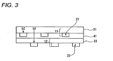
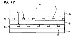
投影型静電容量方式のタッチパネルの代表的な電極の構成は、タッチパネルの視認者側から、上部電極シートと下部電極シートが絶縁体を介して積層されている。以下を、本発明のひとつの態様である、現像方式での電極形成の例として説明する。現像方式においては、上下2枚の電極シートはそれぞれ透明支持体上にハロゲン化銀感光材料が塗布され、電極のパターンを示すマスクを透した露光と現像により、パターン化された現像銀電極が透明支持体上に形成されている。この電極2枚を積層してタッチパネルを構成する際の態様を図2から図4、および図12に示した。図2の態様ではタッチ者が上下電極シートの現像銀細線の表側表面(透明支持体から遠い側の細線表面)b1を視認し、図3の態様では、タッチ者が上下電極シートの現像銀細線の裏側表面(透明支持体から近い側の細線表面)b2を視認する。一方、図4の態様では、タッチ者が上部電極シートの現像銀細線の裏側表面(透明支持体から近い側の表面)b2と、下部電極シートでは現像銀細線の表側表面(透明支持体から遠い側の細線表面)b1とを同時に視認している。更に図12の態様では、タッチ者が上部電極シートでは現像銀細線の表側表面(透明支持体から遠い側の表面)b1と、下部電極シートでは現像銀細線の裏側表面(透明支持体から近い側の細線表面)b2とを同時に視認している。これらの4種の態様において、発明者らは、図4および図12の態様のみが電極間の色ムラを発生させ、図2及び3の態様では電極間の色ムラが観測されないこと、また図2と図3とは、それぞれの電極としては均一な色調であるが、図2と3の電極の色味そのものは異なること、更に図4および図12の態様の色ムラは電極の銀の密度が大きい場合に発生しやすく、従来の写真画像形成程度の銀の密度では発生しにくいことを見出し、以下の発明に至った。
As a result of intensive investigation of the cause of the above-described unevenness in color, the present inventors have reached the present invention from the following facts.
In a typical electrode configuration of a projected capacitive touch panel, an upper electrode sheet and a lower electrode sheet are laminated via an insulator from the viewer side of the touch panel. The following will be described as an example of electrode formation by a developing method, which is one aspect of the present invention. In the development system, the upper and lower electrode sheets are each coated with a silver halide photosensitive material on a transparent support, and the patterned developed silver electrode is transparent by exposure and development through a mask indicating the electrode pattern. It is formed on a support. A mode when the two electrodes are laminated to form a touch panel is shown in FIG. 2 to FIG. 4 and FIG. In the aspect of FIG. 2, the toucher visually recognizes the front side surface (thin surface on the side far from the transparent support) b1 of the developed silver thin wire on the upper and lower electrode sheets. In the embodiment of FIG. The back side surface (the surface of the fine wire closer to the transparent support) b2 is visually recognized. On the other hand, in the embodiment of FIG. 4, the toucher has a back side surface (surface closer to the transparent support) b2 of the developed silver fine wire of the upper electrode sheet, and a front side surface (distant from the transparent support) of the developed silver fine wire in the lower electrode sheet. The fine wire surface b1 on the side is visible at the same time. Further, in the embodiment of FIG. 12, the toucher has a surface on the front side of the developed silver fine line (surface far from the transparent support) b1 in the upper electrode sheet, and a back side surface of the developed silver fine line in the lower electrode sheet (side closer to the transparent support). The fine wire surface b2 is visually recognized at the same time. In these four modes, the inventors have found that only the modes of FIGS. 4 and 12 cause color unevenness between the electrodes, and in the modes of FIGS. 2 and 3, no color unevenness between the electrodes is observed. 2 and FIG. 3 have a uniform color tone as each electrode, but the color of the electrodes in FIGS. 2 and 3 are different, and the color unevenness in the embodiments in FIGS. 4 and 12 is the density of silver in the electrodes. Has been found to be difficult to occur at a silver density comparable to that of conventional photographic image formation, leading to the following invention.
<1>
透明支持体上にパターニングされた電極が形成された透明電極シートであって、上記電極が線幅10μm以下の金属細線からなり、上記電極の透明支持体から遠い側の表面の反射色度b 1 * と、上記電極の透明支持体に近い側の表面の反射色度b 2 * との差の絶対値が2以下(|△b * |=|b 1 * −b 2 * |≦2)であることを特徴とする透明電極シート。
<2>
上記金属細線の線幅が2μm以上、6μm以下であることを特徴とする<1>に記載の透明電極シート。
<3>
上記b 1 * と上記b 2 * との差の絶対値が1.5以下(|△b * |=|b 1 * −b 2 * |≦1.5)であることを特徴とする<1>又は<2>に記載の透明電極シート。
<4>
上記b 1 * と上記b 2 * との差の絶対値が1.0以下(|△b * |=|b 1 * −b 2 * |≦1.0)であることを特徴とする<1>〜<3>のいずれか1項に記載の透明電極シート。
<5>
上記b 1 * が0以下(b 1 * ≦0)であることを特徴とする<1>〜<4>のいずれか1項に記載の透明電極シート。
<6>
上記b 1 * と上記b 2 * とが、−2.0<b 1 * ≦0、かつ−1.0<b 2 * ≦1.0であることを特徴とする<1>〜<5>のいずれか1項に記載の透明電極シート。
<7>
上記b 1 * と上記b 2 * とが、−1.5<b 1 * ≦−0.3、かつ−0.7<b 2 * ≦0.5であることを特徴とする<1>〜<6>のいずれか1項に記載の透明電極シート。
<8>
上記b 1 * と上記b 2 * とが、−1.0<b 1 * ≦−0.5、かつ−0.5<b 2 * ≦0.2であることを特徴とする<1>〜<7>のいずれか1項に記載の透明電極シート。
<9>
上記電極を構成する金属細線の厚みが0.1μm以上、1.5μm以下であることを特徴とする<1>〜<8>のいずれか1項に記載の透明電極シート。
<10>
上記電極を構成する金属細線の厚みが0.2μm以上、0.8μm以下であることを特徴とする<1>〜<9>のいずれか1項に記載の透明電極シート。
<11>
上記金属細線が金、銀、又は銅から選択される金属材料で形成されることを特徴とする<1>〜<10>のいずれか1項に記載の透明電極シート。
<12>
上記電極が上記金属細線からなる格子で形成され、上記格子の単位格子の一辺の長さが50〜500μmであることを特徴とする<1>〜<11>のいずれか1項に記載の透明電極シート。
<13>
上記電極が上記金属細線からなる格子で形成され、上記格子の単位格子の一辺の長さが150〜300μmであることを特徴とする<1>〜<11>のいずれか1項に記載の透明電極シート。
<14>
上記透明支持体上にパターニングされた電極が、透明支持体上に形成されたハロゲン化銀乳剤を含む1以上の感光層を露光現像して形成されたものであり、上記感光層に含まれる銀とバインダーの体積比(銀/バインダー比)が1.0以上である層を有することを特徴とする<1>〜<13>のいずれか1項に記載の透明電極シート。
<15>
<1>〜<14>のいずれか1項に記載の透明電極シートを2枚用い、上記2枚の電極側が向き合って対抗するように絶縁体を介して積層したタッチパネルであって、2枚の電極シートの電極の導通の向きが略直交していることを特徴とする静電容量式タッチパネル。
<16>
透明支持体の両面上にパターニングされた電極が形成された透明電極シートであって、上記電極が線幅10μm以下の金属細線からなり、一方の面に形成された電極の透明支持体から遠い側の表面の反射色度b 1 * と、他方の面に形成された電極の透明支持体に近い側の表面の反射色度b 2 * との差の絶対値が2以下(|△b * |=|b 1 * −b 2 * |≦2)であることを特徴とする透明電極シート。
<17>
上記b 1 * と上記b 2 * との差の絶対値が1.5以下(|△b * |=|b 1 * −b 2 * |≦1.5)であることを特徴とする<16>に記載の透明電極シート。
<18>
上記b 1 * と上記b 2 * との差の絶対値が1.0以下(|△b * |=|b 1 * −b 2 * |≦1.0)であることを特徴とする<16>又は<17>に記載の透明電極シート。
<19>
上記b 1 * と上記b 2 * とが、−2.0<b 1 * ≦0、かつ−1.0<b 2 * ≦1.0であることを特徴とする<16>〜<18>のいずれか1項に記載の透明電極シート。
<20>
上記電極を構成する金属細線の厚みが0.1μm以上、1.5μm以下であることを特徴とする<16>〜<19>のいずれか1項に記載の透明電極シート。
<21>
上記金属細線が金、銀、又は銅から選択される金属材料で形成されることを特徴とする<16>〜<20>のいずれか1項に記載の透明電極シート。
<22>
上記電極が上記金属細線からなる格子で形成され、上記格子の単位格子の一辺の長さが50〜500μmであることを特徴とする<16>〜<21>のいずれか1項に記載の透明電極シート。
<23>
<16>〜<22>のいずれか1項に記載の透明電極シートを用いたことを特徴とするタッチパネル。
本発明は、上記<1>〜<23>に関するものであるが、その他の事項(たとえば下記[1]〜[26]に記載した事項)についても参考のために記載した。
[1]透明支持体上にパターニングされた電極が形成された透明電極シートであって、透明支持体に遠い側の電極表面の反射色度b1 *と、透明支持体に近い側の電極表面の反射色度b2 *との差の絶対値が2以下(|△b*|=|b1 *−b2 *|≦2)であることを特徴とする透明電極シート。
[2]該電極の反射色度b1 *と、反射色度b2 *との差の絶対値が1.5以下、更に好ましくは1.0以下であることを特徴とする項1に記載の透明電極シート。
[3]該電極の表面を透明支持体から遠い側から測定した反射色度b1 *がb1 *≦0であることを特徴とする項1又は項2に記載の透明電極シート。
[4]該電極が透明支持体上に形成されたハロゲン化銀乳剤を含む1以上の感光層を露光現像して形成されたものであり、該感光層に含まれる銀とバインダーの体積比(銀/バインダー比)が、1.0以上である層を有することを特徴とする項1〜3のいずれか1項に記載の透明電極シート。
[5]該感光層に含まれる銀とバインダーの体積比(銀/バインダー比)が1.5以上である層を有することを特徴とする項4に記載の透明電極シート。
<1>
A transparent electrode sheet on which a patterned electrode is formed on a transparent support, wherein the electrode is made of a fine metal wire having a line width of 10 μm or less, and the reflection chromaticity b 1 of the surface of the electrode far from the transparent support is * and the absolute value of the difference between the reflection chromaticity b 2 * of the transparent support on the side near the surface of the electrode 2 or less (| △ b * | = | b 1 * -b 2 * | ≦ 2) in A transparent electrode sheet characterized by being.
<2>
The transparent electrode sheet according to <1>, wherein a line width of the thin metal wire is 2 μm or more and 6 μm or less.
<3>
<1 where the absolute value of the difference between b 1 * and b 2 * is 1.5 or less (| Δb * | = | b 1 * −b 2 * | ≦ 1.5) > Or <2>.
<4>
<1 where the absolute value of the difference between b 1 * and b 2 * is 1.0 or less (| Δb * | = | b 1 * −b 2 * | ≦ 1.0) The transparent electrode sheet according to any one of> to <3>.
<5>
The b 1 * is 0 or less (b 1 * ≦ 0) characterized in that it is a <1> to transparent electrode sheet according to any one of <4>.
<6>
<1> to <5>, wherein b 1 * and b 2 * are −2.0 <b 1 * ≦ 0 and −1.0 <b 2 * ≦ 1.0. The transparent electrode sheet according to any one of the above.
<7>
The b 1 * and the b 2 * and is characterized in that it is a -1.5 <b 1 * ≦ -0.3 and -0.7 <b 2 * ≦ 0.5, <1> ~ The transparent electrode sheet according to any one of <6>.
<8>
The b 1 * and the b 2 * and is characterized in that -1.0 <b 1 * ≦ -0.5, and a -0.5 <b 2 * ≦ 0.2 < 1> ~ The transparent electrode sheet according to any one of <7>.
<9>
<1>-<8> The transparent electrode sheet according to any one of <1> to <8>, wherein a thickness of the fine metal wire constituting the electrode is 0.1 μm or more and 1.5 μm or less.
<10>
<1>-<9> The transparent electrode sheet according to any one of <1> to <9>, wherein a thickness of the thin metal wire constituting the electrode is 0.2 μm or more and 0.8 μm or less.
<11>
<1>-<10> The transparent electrode sheet according to any one of <1> to <10>, wherein the thin metal wire is formed of a metal material selected from gold, silver, or copper.
<12>
The transparent electrode according to any one of <1> to <11>, wherein the electrode is formed of a grid made of the fine metal wires, and a length of one side of the unit grid of the grid is 50 to 500 μm. Electrode sheet.
<13>
<1>-<11> The transparent according to any one of <1> to <11>, wherein the electrode is formed of a grid made of the thin metal wires, and a length of one side of the unit grid of the grid is 150 to 300 μm. Electrode sheet.
<14>
The electrode patterned on the transparent support is formed by exposing and developing one or more photosensitive layers containing a silver halide emulsion formed on the transparent support. Silver contained in the photosensitive layer The transparent electrode sheet according to any one of <1> to <13>, wherein the transparent electrode sheet has a layer having a volume ratio of silver and binder (silver / binder ratio) of 1.0 or more.
<15>
<1>-<14> The touch panel which laminated | stacked via the insulator so that the two electrode sides of any one of <1>-<14> were laminated | stacked so that the said 2 electrode side might face and oppose, A capacitive touch panel, wherein the direction of conduction of the electrodes of the electrode sheet is substantially orthogonal.
<16>
A transparent electrode sheet in which patterned electrodes are formed on both surfaces of a transparent support, wherein the electrode is made of a fine metal wire having a line width of 10 μm or less, and the side of the electrode formed on one side far from the transparent support The absolute value of the difference between the reflection chromaticity b 1 * of the surface of the electrode and the reflection chromaticity b 2 * of the surface near the transparent support of the electrode formed on the other surface is 2 or less (| Δb * | = | B 1 * −b 2 * | ≦ 2).
<17>
The absolute value of the difference between the b 1 * and the b 2 * is 1.5 or less (| Δb * | = | b 1 * −b 2 * | ≦ 1.5) <16 > Transparent electrode sheet.
<18>
The absolute value of the difference between the b 1 * and the b 2 * is 1.0 or less (| Δb * | = | b 1 * −b 2 * | ≦ 1.0) <16 > Or <17>.
<19>
<16> to <18>, wherein b 1 * and b 2 * are −2.0 <b 1 * ≦ 0 and −1.0 <b 2 * ≦ 1.0. The transparent electrode sheet according to any one of the above.
<20>
<16>-<19> The transparent electrode sheet according to any one of <16> to <19>, wherein a thickness of the fine metal wire constituting the electrode is 0.1 μm or more and 1.5 μm or less.
<21>
<16>-<20> The transparent electrode sheet according to any one of <16> to <20>, wherein the thin metal wire is formed of a metal material selected from gold, silver, or copper.
<22>
The transparent electrode according to any one of <16> to <21>, wherein the electrode is formed of a grid made of the fine metal wires, and a length of one side of the unit grid of the grid is 50 to 500 μm. Electrode sheet.
<23>
<16>-<22> The touch panel using the transparent electrode sheet of any one of <22>.
The present invention relates to the above <1> to <23>, but other matters (for example, the matters described in [1] to [26] below) are also described for reference.
[1] A transparent electrode sheet on which a patterned electrode is formed on a transparent support, the reflection chromaticity b 1 * of the electrode surface far from the transparent support, and the electrode surface near the transparent support The transparent electrode sheet, wherein the absolute value of the difference from the reflection chromaticity b 2 * is 2 or less (| Δb * | = | b 1 * −b 2 * | ≦ 2).
[2] The absolute value of the difference between the reflected chromaticity b 1 * and the reflected chromaticity b 2 * of the electrode is 1.5 or less, more preferably 1.0 or less. Transparent electrode sheet.
[3] The transparent electrode sheet according to
[4] The electrode is formed by exposing and developing one or more photosensitive layers containing a silver halide emulsion formed on a transparent support, and the volume ratio of silver and binder contained in the photosensitive layer ( Item 4. The transparent electrode sheet according to any one of
[5] The transparent electrode sheet according to item 4, which has a layer in which the volume ratio (silver / binder ratio) of silver and binder contained in the photosensitive layer is 1.5 or more.
[6]該ハロゲン化銀乳剤を含む感光層が、少なくとも1種のメルカプト化合物を含み、その感光層中のメルカプト化合物の含有量が、透明支持体に近い表面側の感光層で高いことを特徴とする項1〜5のいずれか1項に記載の透明電極シート。
[7]該メルカプト化合物が、N−H構造を有する5員環アゾール又はN−H構造を有する6員環アジンを骨格とするメルカプト化合物であり、N−H構造とはアゾール類又はアジン類に含まれる窒素−水素結合を意味し、該水素は解離可能であることを特徴とする項6に記載の透明電極シート。
[8]該メルカプト化合物が、2-メルカプトベンゾイミダゾールの4位から7位のいずれかにSO3 M基を置換基として有し、更に水素原子、ヒドロキシル基、低級アルキル基、低級アルコキシ基、カルボキシル基、ハロゲン基、スルホ基から選ばれる少なくとも1つの基を置換基として有し、Mはアルカリ金属原子又はアンモニウム基であることを特徴とする項6に記載の透明電極シート。
[9]該感光層の少なくとも1つに含まれるメルカプト化合物の量は、メルカプト化合物と同じ層に含まれるハロゲン化銀乳剤中の銀1g(グラム)に対して、0.1mg以上、15mg以下であることを特徴とする項1〜8のいずれか1項に記載の透明電極シート。
[6] The photosensitive layer containing the silver halide emulsion contains at least one mercapto compound, and the content of the mercapto compound in the photosensitive layer is high in the photosensitive layer on the surface side close to the transparent support. The transparent electrode sheet according to any one of
[7] The mercapto compound is a mercapto compound having a 5-membered ring azole having an NH structure or a 6-membered ring azine having an NH structure as a skeleton, and the NH structure is an azole or azine. Item 7. The transparent electrode sheet according to Item 6, which means a nitrogen-hydrogen bond contained, and the hydrogen is dissociable.
[8] The mercapto compound has an SO 3 M group as a substituent at any of the 4th to 7th positions of 2-mercaptobenzimidazole, and further has a hydrogen atom, a hydroxyl group, a lower alkyl group, a lower alkoxy group, a carboxyl group Item 7. The transparent electrode sheet according to Item 6, having at least one group selected from a group, a halogen group, and a sulfo group as a substituent, wherein M is an alkali metal atom or an ammonium group.
[9] The amount of the mercapto compound contained in at least one of the photosensitive layers is 0.1 mg or more and 15 mg or less with respect to 1 g (gram) of silver in the silver halide emulsion contained in the same layer as the mercapto compound. Item 9. The transparent electrode sheet according to any one of
[10]該ハロゲン化銀乳剤が塩臭化銀乳剤であり、透明支持体に近い表面側の感光層のハロゲン化銀乳剤の現像液に対する溶解度が、透明支持体から遠い表面側の感光層のハロゲン化銀乳剤の現像液に対する溶解度よりも低いことを特徴とする項1〜9のいずれか1項に記載の透明電極シート。
[11]該塩臭化銀乳剤含有感光層全体における平均の臭化銀含有率が10%以上、50%以下であることを特徴とする項1〜10のいずれか1項に記載の透明電極シート。
[12]該透明支持体側の感光層の塩臭化銀乳剤の臭化銀含有率が、透明支持体から遠い表面側の感光層の臭化銀含有率よりも高いことを特徴とする項1〜11のいずれか1項に記載の透明電極シート。
[13]該透明支持体から遠い表面側の感光層に含まれる臭化銀含有率よりも、透明支持体に近い表面側の感光層の臭化銀含有率が10%以上高いことを特徴とする項12に記載の透明電極シート。
[10] The silver halide emulsion is a silver chlorobromide emulsion, and the solubility of the photosensitive layer on the surface side close to the transparent support in the developer of the silver halide emulsion is that of the photosensitive layer on the surface side remote from the transparent support.
[11] The transparent electrode as described in any one of [1] to [10], wherein the average silver bromide content in the entire photosensitive layer containing the silver chlorobromide emulsion is 10% or more and 50% or less. Sheet.
[12] The silver bromide content of the silver chlorobromide emulsion in the photosensitive layer on the transparent support side is higher than the silver bromide content in the photosensitive layer on the surface side remote from the transparent support. The transparent electrode sheet of any one of -11.
[13] The silver bromide content in the surface-side photosensitive layer near the transparent support is 10% or more higher than the silver bromide content in the surface-side photosensitive layer far from the transparent support. Item 13. The transparent electrode sheet according to
[14]該透明支持体に近い側の感光層に含まれる銀とバインダーの体積比が1.0未満であることを特徴とする項1〜13のいずれか1項に記載の透明電極シート。
[15]該透明支持体に近い側の感光層及び透明支持体から遠い側の感光層に含まれる銀とバインダーの体積比が1.0未満であることを特徴とする項1〜13のいずれか1項に記載の透明電極シート。
[16]該パターニングされた電極を構成する導電性細線の線幅が10μm以下であり、好ましくは1μm以上、10μm以下であることを特徴とする項1〜15のいずれか1項に記載の透明電極シート。
[17]該導電性細線の線幅が2μm以上、6μm以下であることを特徴とする項1〜16のいずれか1項に記載の透明電極シート。
[14] The transparent electrode sheet according to any one of [1] to [13], wherein the volume ratio of silver and binder contained in the photosensitive layer on the side close to the transparent support is less than 1.0.
[15] The volume ratio of silver and binder contained in the photosensitive layer on the side close to the transparent support and the photosensitive layer on the side far from the transparent support is less than 1.0, The transparent electrode sheet according to
[16] The transparent according to any one of
[17] The transparent electrode sheet according to any one of [1] to [16], wherein a line width of the conductive fine wire is 2 μm or more and 6 μm or less.
[18]該導電性細線の厚みが0.1μm以上、1.5μm以下であることを特徴とする項1〜17のいずれか1項に記載の透明電極シート。
[19]該導電性細線の厚みが0.2μm以上、0.8μmであることを特徴とする項1〜17のいずれか1項に記載の透明電極シート。
[20]透明支持体上にパターニングされた電極が形成された透明電極シートであって、透明支持体に遠い側の電極表面の反射色度b1 *と、透明支持体に近い側の電極表面の反射色度b2 *とが、−2.0<b1 *≦0、かつ−1.0<b2 *≦1.0 であることを特徴とする項1〜19のいずれか1項に記載の透明電極シート。
[21]透明支持体の両面上にパターニングされた電極が形成された透明電極シートであって、一方の面の支持体から遠くに位置する電極表面の反射色度b1 *と、他方の面の支持体に近く位置する電極表面の反射色度b2 *との差の絶対値が2以下(|△b*|=|b1 *−b2 *|≦2)であることを特徴とする項1〜19のいずれか1項に記載の透明電極シート。
[22]項21の|△b*|が1以下であることを特徴とする透明電極シート。
[23]項21又は22のb1 *が、−2.0<b1 *≦0、かつb2 *が、−1.0<b2 *≦1.0 であることを特徴とする透明電極シート。
[24]項21又は22のb1 *が、−1.0<b1 *≦−0.5、かつb2 *が、−0.5<b2 *≦0.2であることを特徴とする透明電極シート。
[25]項1〜19のいずれか1項に記載の透明電極シートを2枚用い、該2枚の電極側が向き合って対抗するように絶縁体を介して積層したタッチパネルであって、2枚の電極シートの電極の導電性細線の導通の方向が略直交していることを特徴とする静電容量式タッチパネル。
[26]項1〜19のいずれか1項に記載の透明電極シートを2枚用い、該2枚の電極シートの透明支持体側が視認者側となるように、または該2枚の電極シートの電極側が視認者側となるように積層したタッチパネルであって、2枚の電極シートの電極の導電性細線の導通の方向が略直交していることを特徴とするタッチパネル。
[18] The transparent electrode sheet according to any one of
[19] The transparent electrode sheet according to any one of
[20] A transparent electrode sheet on which a patterned electrode is formed on a transparent support, the reflection chromaticity b 1 * of the electrode surface on the side far from the transparent support, and the electrode surface on the side close to the transparent support The reflection chromaticity b 2 * of the formula is any one of
[21] A transparent electrode sheet in which patterned electrodes are formed on both sides of a transparent support, the reflection chromaticity b 1 * of the electrode surface located far from the support on one side, and the other side The absolute value of the difference from the reflection chromaticity b 2 * of the electrode surface located near the support is 2 or less (| Δb * | = | b 1 * −b 2 * | ≦ 2) Item 20. The transparent electrode sheet according to any one of
[22] The transparent electrode sheet according to
[23] Transparent, wherein b 1 * in item 21 or 22 is −2.0 <b 1 * ≦ 0 and b 2 * is −1.0 <b 2 * ≦ 1.0 Electrode sheet.
[24]
[25] A touch panel in which two transparent electrode sheets according to any one of
[26] The two transparent electrode sheets according to any one of
上記の本発明の色調の改良された透明電極シートは、導電材料の表面の色調が改良されているが故に、上記の静電容量式のタッチパネルに用いる電極材料のみならず、人の視認性と導電性に係わる材料であればすべてに応用することができる。これらの応用可能なものを例示する。抵抗膜式タッチパネルに用いられる透明導電シート、画像表示装置の内部からの電磁波を遮蔽するための電磁波シールドシートなどは、本発明の電極のパターニングにより形成される導電性細線のパターンを変更するだけで本発明の技術を利用できる。また、本発明の電極の抵抗値を調整することにより、発熱体シートや帯電防止シートを作成することもできる。 The above-described transparent electrode sheet with improved color tone according to the present invention has improved color tone on the surface of the conductive material, so that not only the electrode material used for the capacitive touch panel, but also human visibility and Any material that is conductive can be applied. These are applicable. Transparent conductive sheets used for resistive film type touch panels, electromagnetic wave shielding sheets for shielding electromagnetic waves from the inside of image display devices, etc., simply change the pattern of conductive thin wires formed by patterning the electrodes of the present invention. The technology of the present invention can be used. Further, a heating element sheet or an antistatic sheet can be prepared by adjusting the resistance value of the electrode of the present invention.
本発明の透明電極シートは、図2〜図4、および図12に示した態様のいずれにも適用でき、均一で色味差の小さい画面が得られ、静電容量方式のタッチパネルを設計する自由度が大きい。本発明の電極シートは低抵抗であるため、大面積にしても応答性に優れ、色味のほか、画面として見たときに異物やモアレなどを感じさせない視認性に優れ、かつマルチタッチが可能なタッチパネルを得ることができる。更には現像処理という安定した工程により電極が形成できるため、加工、製造の安定性に優れ、品質の安定したタッチパネルを得ることができる。また、本発明の透明電極シートを応用すると、色調に優れた抵抗膜式タッチパネルに用いられる透明導電シート、電磁波シールドシート、発熱体シートや帯電防止シートを得ることができる。 The transparent electrode sheet of the present invention can be applied to any of the embodiments shown in FIG. 2 to FIG. 4 and FIG. 12, and a uniform and small color difference screen can be obtained, so that a capacitive touch panel can be freely designed. The degree is great. Since the electrode sheet of the present invention has low resistance, it has excellent responsiveness even in a large area, and it has excellent visibility that does not feel foreign matter or moire when viewed as a screen, as well as multi-touch. Touch panel can be obtained. Furthermore, since the electrode can be formed by a stable process such as development processing, a touch panel having excellent processing and manufacturing stability and stable quality can be obtained. Moreover, when the transparent electrode sheet of the present invention is applied, a transparent conductive sheet, an electromagnetic wave shield sheet, a heating element sheet and an antistatic sheet used for a resistive film type touch panel excellent in color tone can be obtained.
以下、本発明に係る電極シート、電極シートの製造方法及びタッチパネルの実施の形態例を図1〜図11を参照しながら説明する。なお、本明細書において「〜」は、その前後に記載される数値を下限値及び上限値として含む意味として使用される。 Hereinafter, embodiments of an electrode sheet, an electrode sheet manufacturing method, and a touch panel according to the present invention will be described with reference to FIGS. In the present specification, “to” is used as a meaning including numerical values described before and after the lower limit value and the upper limit value.
本発明の電極シートは、透明支持体上にパターニングされた電極が形成された透明電極シートであって、透明支持体から遠い側の電極表面の反射色度b1 *と、透明支持体に近い側の電極表面の反射色度b2 *との差の絶対値が2以下(|△b*|=|b1 *−b2 *|≦2)である。 The electrode sheet of the present invention is a transparent electrode sheet in which a patterned electrode is formed on a transparent support, and the reflection chromaticity b 1 * of the electrode surface far from the transparent support is close to the transparent support. The absolute value of the difference from the reflection chromaticity b 2 * of the electrode surface on the side is 2 or less (| Δb * | = | b 1 * −b 2 * | ≦ 2).
本発明は、課題を解決するための手段項の冒頭に説明したように、電極シートをどの方向から眺めるかによって観察される色味が異なるとの課題を解決することを目的としている。色味が異なる現象を再度説明する。図5の矢印b1は、電極シート11の電極22の透明支持体から遠い側の表面の反射色度を測定する場合(b1方向とも言う)を指し、矢印b2は、電極シート11の電極22の表面を透明支持体33に近い側から反射色度を測定する場合(b2方向とも言う)を指し、この2つの方向から反射色度を測定したときの電極の反射色度差が視認される程度に異なることが課題である。本発明は、b1方向からの反射色度b1 *と、b2方向からの反射色度b2 *との差の絶対値を2以下とすれば、図4および図12のような配置に電極シートを配置しても色ムラとして視認されにくいことに基づく発明である。
An object of the present invention is to solve the problem that the observed color is different depending on which direction the electrode sheet is viewed, as described at the beginning of the means for solving the problem. The phenomenon of different colors will be explained again. An arrow b 1 in FIG. 5 indicates a case where the reflection chromaticity of the surface of the
なお、反射色度b*は、L*a*b*表色系で定義される特性値である。L*a*b*表色系は、国際照明委員会(CIE)において1976年に定められた表色の方法であり、本発明におけるL*値、a*値、b*値は、JIS−Z8729:1994に規定される方法によって測定して得られた値である。JIS−Z8729の測定方法としては、反射による測定方法、透過による測定方法があるが、本発明では反射で測定した値を用いる。
L*a*b*表色系におけるL*値、a*値、b*値は、広く知られているように、L*値が明度、a*値とb*値とが、色相と彩度を表している。具体的には、a*値が正の符号であれば赤色の色相、負の符号であれば緑色の色相であることを示す。b*値が正であれば黄色の色相、負であれば青色の色相である。また、a*値とb*値とも、絶対値が大きいほどその色の彩度が大きく鮮やかな色であることを示し、絶対値が小さいほど彩度が小さいことを示す。
本発明においては、a*値は観察する方向(b1方向とb2方向)での変化が小さい。一方、b*値は電極の観察する方向による変化がa*値よりおおきく、具体的には、黄色味から青色味へかわることで色ムラとして視認されやすい。測定方法の詳細は実施例の項に記載する。
The reflection chromaticity b * is a characteristic value defined by the L * a * b * color system. The L * a * b * color system is a color specification method defined by the International Commission on Illumination (CIE) in 1976, and the L * value, a * value, and b * value in the present invention are JIS- Z8729: A value obtained by measurement by the method defined in 1994. As a measuring method of JIS-Z8729, there are a measuring method by reflection and a measuring method by transmission. In the present invention, a value measured by reflection is used.
L * a * b * L * values in a color system, a * value, b * value, as is well known, L * value is brightness, and the a * value and b * value, hue and chroma Represents degrees. Specifically, if the a * value has a positive sign, it indicates a red hue, and if it has a negative sign, it indicates a green hue. If the b * value is positive, the hue is yellow, and if it is negative, the hue is blue. Further, for both the a * value and the b * value, the larger the absolute value, the larger the saturation of the color, and the brighter the color, and the smaller the absolute value, the smaller the saturation.
In the present invention, a * value is less change in the viewing direction (b 1 direction and the b 2 direction). On the other hand, the b * value changes more greatly than the a * value depending on the viewing direction of the electrode. Specifically, the b * value is easily recognized as color unevenness by changing from yellow to blue. Details of the measurement method are described in the Examples section.
図4の電極の積層例のように、タッチ者が電極の透明支持体から遠い表面側の反射色度(b1 *)と支持体に近い側の電極表面の反射色度(b2 *)とを同時に視認する場合の色ムラを改良するためには、反射色度b1 *と、反射色度b2 *との差(△b*)の絶対値が以下の関係を満たす必要がある。
|△b*|=|b1 *−b2 * |≦2
更に好ましくは、|△b*|≦1.5、特に好ましくは、|△b*|≦1.0である。
As shown in the electrode stacking example of FIG. 4, the reflective chromaticity (b 1 * ) on the surface side where the toucher is far from the transparent support of the electrode and the reflection chromaticity (b 2 * ) of the electrode surface on the side close to the support. In order to improve the color unevenness in the case where the chromaticity is simultaneously viewed, the absolute value of the difference (Δb * ) between the reflected chromaticity b 1 * and the reflected chromaticity b 2 * needs to satisfy the following relationship: .
| Δb * | = | b 1 * −b 2 * | ≦ 2
More preferably, | Δb * | ≦ 1.5, and particularly preferably | Δb * | ≦ 1.0.
また、観察したときの色調は、視覚上、黒と視認しやすくすることが好ましい。b1 *及びb2 *の測定値は、0の近傍がニュートラルとされるが、本発明においては以下に設定すると、視認者が黒と視認しやすい。
本発明においては、b1 *としては、−2.0<b1 *≦0が好ましく、−1.5<b1 *≦−0.3がより好ましく、−1.0<b1 *≦−0.5が特に好ましい。
b2 *としては、−1.0<b2 *≦1.0が好ましく、−0.7<b2 *≦0.5がより好ましく、−0.5<b2 *≦0.2が特に好ましい。
b1 *及びb2 *の組み合わせとしては、−2.0<b1 *≦0、かつ−1.0<b2 *≦1.0 であることが好ましく、−1.5<b1 *≦−0.3、かつ−0.7<b2 *≦0.5がより好ましく、−1.0<b1 *≦−0.5、かつ−0.5<b2 *≦0.2が特に好ましい。
また、透明電極の構成が一枚の透明支持体の両面上にパターニングされた電極が形成されたものである場合には、図12に示したように一方面の電極表面の反射色度b1 *と、他方面の電極表面の反射色度b2 *との差の絶対値が2以下(|△b*|=|b1 *−b2 *|≦2)であるようにしてもよい。一枚の透明支持体の両面上にパターニングされた電極が形成されたものの場合、一方面の電極表面(反射色度b1 *)と、他方の面の電極の支持体の接する面(反射色度b2 *)とが、タッチ者に視認されるからであり、両面の反射色度の差が色ムラのように見えることがあるので、上記のように反射色度を調整することが好ましい。
Moreover, it is preferable that the color tone when observed is easily visually recognized as black. The measured values of b 1 * and b 2 * are neutral in the vicinity of 0. However, in the present invention, when set as follows, the viewer can easily recognize black.
In the present invention, b 1 * is preferably −2.0 <b 1 * ≦ 0, more preferably −1.5 <b 1 * ≦ −0.3, and −1.0 <b 1 * ≦ -0.5 is particularly preferred.
As b 2 * , −1.0 <b 2 * ≦ 1.0 is preferable, −0.7 <b 2 * ≦ 0.5 is more preferable, and −0.5 <b 2 * ≦ 0.2 is satisfied. Particularly preferred.
The combination of b 1 * and b 2 * is preferably −2.0 <b 1 * ≦ 0 and −1.0 <b 2 * ≦ 1.0, and −1.5 <b 1 * ≦ −0.3 and −0.7 <b 2 * ≦ 0.5 are more preferable, −1.0 <b 1 * ≦ −0.5, and −0.5 <b 2 * ≦ 0.2 Is particularly preferred.
In addition, when the transparent electrode has a structure in which patterned electrodes are formed on both surfaces of a single transparent support, the reflection chromaticity b 1 of the electrode surface on one surface as shown in FIG. * and the absolute value of the difference between the reflection chromaticity b 2 * of the other surface of the electrode surface 2 or less (| △ b * | = | b 1 * -b 2 * | ≦ 2) may be a . In the case where patterned electrodes are formed on both surfaces of a single transparent support, the electrode surface (reflection chromaticity b 1 * ) on one side and the surface (reflection color) of the electrode support on the other side Degree b 2 * ) is visually recognized by the toucher, and the difference in reflection chromaticity on both sides may appear as color unevenness. Therefore, it is preferable to adjust the reflection chromaticity as described above. .
次に、本発明の透明支持体上に形成されたパターニングされた電極について、本発明の透明電極シートが好ましく用いられる静電容量方式のタッチパネルと関連させながら説明する。従来の静電容量方式のタッチパネルでは、電極材料として透明電極材料であるITO薄膜をバー電極として使用されてきたが、本発明においてはITOより低抵抗の材料を用いた導電性細線の組み合わせにより電極を形成しているため、これをパターニングされた電極と呼んでいる。上記低抵抗の材料は、不透明な材料であり、金、銀、銅などの金属材料が使用される。
本発明の透明電極シートを用いる静電容量方式のタッチパネルは、例えば、図1の断面図に示したように、絶縁層41を介して2枚の電極が対向するように配置されている。図1では上部電極シート11の下側に上部電極の導電性細線21が形成されており、下部電極の導電性細線22は下部電極シート12の上側に形成されている。
上部電極シート11、絶縁層41、下部電極シート12の積層体を、簡略化のために絶縁層41を除いて斜視したのが図8である。上部電極シート11及び下部電極シート12を構成する複数の電極は、一つ一つの電極が、静電容量を感知する複数の導電性格子部14A及び14Bと、格子と格子を繋ぐ導電性の連結部16A及び16Bからなり、これらの電極と外部制御部を引き出し線18A、18Bが繋いでいる。図8では、導電性の格子部をメッシュ様に表示しているが、ITOなどの菱形の透明導電性膜を結合したパターン(ダイヤモンドパターンと呼ばれている)を細線化して用いてもよい。図8では上部電極シート11と下部電極シート12の電極の導通方向がほぼ直交するように配置されている。上部電極シート11と下部電極シート12の電極のそれぞれの電極の本数、導電性の格子部の数は、パネルの大きさや制御のしやすさにより変更することができる。
図9及び図10は、それぞれ、図8の上部電極シート11及び下部電極シート12の導電性格子部14A及び14Bと、格子と格子を繋ぐ導電性の連結部16A及び16Bとを取り出した図である。導電性格子部14Aは、導電性細線21で構成される正方格子と、正方格子の周辺に配置され、多数の短線からなるダミー細線19、電極方向に導電性格子部14Aを連結する導電性の連結部16Aが記載されている。導電性の連結部16Aは、予期しない断線故障により電極が機能しなくなることを防ぐため、単一の細線での連結ではなく、複数の細線による連結としている。
図10の導電性格子部14B及び16Bについても、上記の導電性格子部14A及び16Aと同様な説明ができる。
なお、本発明の透明電極シートを用いる静電容量方式のタッチパネルの構成は、上記態様に限定されず、2つの電極がX-Y方向で直交して配置される、いわゆるX-Yマトリクスタイプのものが挙げられる。
Next, the patterned electrode formed on the transparent support of the present invention will be described in relation to a capacitive touch panel in which the transparent electrode sheet of the present invention is preferably used. In the conventional capacitive type touch panel, an ITO thin film, which is a transparent electrode material, has been used as a bar electrode as an electrode material. However, in the present invention, an electrode is formed by a combination of conductive thin wires using a material having a resistance lower than that of ITO. This is called a patterned electrode. The low resistance material is an opaque material, and a metal material such as gold, silver, or copper is used.
The capacitive touch panel using the transparent electrode sheet of the present invention is disposed so that two electrodes face each other with an insulating
FIG. 8 is a perspective view of the laminated body of the
9 and 10 are views in which the
The
Note that the configuration of the capacitive touch panel using the transparent electrode sheet of the present invention is not limited to the above-described embodiment, and is a so-called XY matrix type in which two electrodes are arranged orthogonally in the XY direction. Things.
図11は、図8をタッチ者側から透視した場合の電極線の見え方を示している。本発明の上部電極シート11及び下部電極シート12を用いた図11は、均一な正方格子となり、視認しやすいパネルを構成できる。なお、図11では格子が直線で形成されているように見えるが、直線部分と、2本の短線からなる部分がある。この様子を示したのが図11の○印の部分を拡大した下図であり、左側の実線部は上部電極シートの導電性格子部14Aの導電性細線21の一部を表し、同じく実線の19(21)は、導電性格子部14Aの周囲のダミー細線である。同様に、右側の点線部は下部電極シートの導電性格子部14Bの導電性細線22の一部を表し、同じく点線の19(22)は、導電性格子部14Bの周囲のダミー細線である。このように視覚的には1本の直線に見えても実際には導電性細線21と22は導通しないし、ダミー細線19とも導通しない。
上記から理解できるように、本発明に用いられるダミー細線19は、視認性改良のために用いられる細線であり、図9及び図10で記載されるように、ダミー細線は正方格子の長線の両端部の延長線上に形成され、導電性格子部とは導通しないように断線されている。ダミー細線の長さは、電極部分の単位格子の辺長の1/2以下である。
FIG. 11 shows how the electrode lines appear when FIG. 8 is seen through from the toucher side. FIG. 11 using the
As can be understood from the above, the dummy
以下では、上部電極シート11を例にとり電極の詳細について説明する。従来の電極を形成してきたITOのダイヤモンドパターンは、ITOの抵抗値が高いため大画面への適用が困難であり、本発明ではダイヤモンド部分を低抵抗の細線(例えば、金、銀、銅などの金属材料)からなるメッシュあるいは格子で形成し、低抵抗と画面の明るさを担保している。以下、正方格子での説明とするが、長方格子などの使用を妨げるものではない。
導電性の格子部を形成する導電性細線の線幅は10μm以下であり、1μm以上、10μm以下であることが好ましく、1μm以上、6μm以下であることがより好ましい。1μm以上、10μm以下の範囲であると、低抵抗の電極を比較的容易に形成できる。
導電性の格子部を形成する導電性細線の厚みは、0.1μm以上、1.5μm以下であることが好ましく、0.2μm以上、0.8μm以下であることがより好ましい。0.1μm以上、1.5μm以下の範囲であると、低抵抗の電極で、耐久性に優れた電極を比較的容易に形成できる。
Below, the
The line width of the thin conductive wires forming the conductive lattice portion is 10 μm or less, preferably 1 μm or more and 10 μm or less, and more preferably 1 μm or more and 6 μm or less. When the thickness is in the range of 1 μm or more and 10 μm or less, a low-resistance electrode can be formed relatively easily.
The thickness of the conductive thin wire forming the conductive lattice portion is preferably 0.1 μm or more and 1.5 μm or less, and more preferably 0.2 μm or more and 0.8 μm or less. When the thickness is in the range of 0.1 μm or more and 1.5 μm or less, a low-resistance electrode that is excellent in durability can be formed relatively easily.
本発明の導電性格子部14A及び14Bの一辺の長さは、3〜10mmであることが好ましく、4〜6mmであることがより好ましい。一辺の長さが、3〜10mmであると、感知する静電容量の不足による検出不良になる可能性や、位置検出精度が低下するといった問題を起こしにくい。同様の観点から、導電性格子部を構成する単位格子の一辺の長さは50〜500μmであることが好ましく、150〜300μmであることが更に好ましい。単位格子の辺の長さが上記範囲である場合には、更に透明性も良好に保つことが可能であり、表示装置の前面にとりつけた際に、違和感なく表示を視認することができる。
The length of one side of the
なお、図8のタッチパネルの上下電極は導通方向をほぼ直交としているが、タッチの位置の座標決定に支障の無い限り任意の角度に設定することができる。
更に、図9及び10に例示した正方格子を構成する導電性細線の向きは、X、Y軸に対し45°方向となる。このパネルのX、Y方向を画像表示装置の電極軸の方向として張り合わせると、モアレが発生しにくいという特徴を本発明のタッチパネルは有する。
Note that the upper and lower electrodes of the touch panel in FIG. 8 are substantially perpendicular to the conduction direction, but can be set to any angle as long as there is no hindrance in determining the coordinates of the touch position.
Furthermore, the direction of the conductive thin wires constituting the square lattice illustrated in FIGS. 9 and 10 is 45 ° with respect to the X and Y axes. The touch panel of the present invention has a feature that moire does not easily occur when the X and Y directions of the panel are bonded as the electrode axis direction of the image display device.
以上のパターニングされた電極から構成される電極シートは、1つの電極を1つのITO膜にて形成する構成よりも大幅に電気抵抗(例えば、表面抵抗を測定することで評価される)を低減することが可能となる。従って、本発明の電極シートを用いて例えば投影型静電容量方式のタッチパネルに適用した場合に、応答速度を速めることができ、タッチパネルの大サイズ化を促進させることができる。 The electrode sheet composed of the above patterned electrodes significantly reduces electric resistance (e.g., evaluated by measuring surface resistance), compared to a structure in which one electrode is formed by one ITO film. It becomes possible. Therefore, when the electrode sheet of the present invention is used for, for example, a projected capacitive touch panel, the response speed can be increased and the touch panel can be increased in size.
本発明の電極シートを製造する方法としては、例えば透明基体上に感光性ハロゲン化銀塩を含有する乳剤層を有する感光材料を露光し、現像処理を施すことによって、露光部及び未露光部にそれぞれ金属銀部及び光透過性部を形成して金属細線からなる導電パターンを形成してもよい。
また、透明基体上に形成された銅箔上のフォトレジスト膜を露光、現像処理してレジストパターンを形成し、レジストパターンから露出する銅箔をエッチングすることによって、金属細線からなる導電パターンを形成してもよい。
また、透明基体上に金属微粒子を含むペーストを印刷し、ペーストに金属めっきを行うことによって、金属細線からなる導電パターンを形成してもよい。
また、透明基体上に、金属細線からなる導電パターンをスクリーン印刷版又はグラビア印刷版によって印刷形成するようにしてもよい。
また、透明基体上にめっき前処理材を用いて感光性被めっき層を形成し露光、現像処理した後にめっき処理を施すことにより、露光部及び未露光部にそれぞれ金属部及び光透過性部を形成して金属細線からなる導電パターンを形成してもよい。めっき前処理材を用いる方法のさらに好ましい形態としては、次の(1)、(2)の2通りの形態が挙げられる。なお、下記のより具体的な内容は、特開2003−213437、2006−64923、2006−58797、2006−135271などに開示されている。
(1) 透明基体上に、めっき触媒またはその前駆体と相互作用する官能基を含む被めっき層を塗布し、露光・現像した後にめっき処理して金属部を被めっき材料上に形成させる態様。
(2) 透明基体上に、ポリマー及び金属酸化物を含む下地層と、めっき触媒またはその前駆体と相互作用する官能基を含む被めっき層とをこの順に積層し、露光・現像した後にめっき処理して金属部を被めっき材料上に形成させる態様。
上記方法で製造される電極は、構成材料が不透明であるため電極表面で反射が生じ、その反射の程度は透明支持体から近い側と遠い側では異なる。その反射の程度の差が視認性に影響を与えることになるが、その反射の程度を上述のように制御することで、視認性の高い導電シートを提供することができる。
As a method for producing the electrode sheet of the present invention, for example, a light-sensitive material having an emulsion layer containing a photosensitive silver halide salt is exposed on a transparent substrate and subjected to a development treatment, whereby an exposed portion and an unexposed portion are exposed. A conductive pattern made of a fine metal wire may be formed by forming a metallic silver portion and a light transmitting portion, respectively.
In addition, the photoresist film on the copper foil formed on the transparent substrate is exposed and developed to form a resist pattern, and the copper foil exposed from the resist pattern is etched to form a conductive pattern made of fine metal wires. May be.
Alternatively, a conductive pattern made of fine metal wires may be formed by printing a paste containing metal fine particles on a transparent substrate and performing metal plating on the paste.
Further, a conductive pattern made of fine metal wires may be printed on a transparent substrate by screen printing or gravure printing.
In addition, a photosensitive plating layer is formed on a transparent substrate using a pretreatment material for plating, exposed and developed, and then subjected to a plating treatment, whereby a metal part and a light-transmitting part are formed in an exposed part and an unexposed part, respectively. A conductive pattern made of fine metal wires may be formed. More preferable forms of the method using the plating pretreatment material include the following two forms (1) and (2). The following more specific contents are disclosed in Japanese Patent Application Laid-Open Nos. 2003-213437, 2006-64923, 2006-58797, 2006-135271, and the like.
(1) A mode in which a plating layer containing a functional group that interacts with a plating catalyst or a precursor thereof is applied on a transparent substrate, exposed and developed, and then plated to form a metal portion on the material to be plated.
(2) On the transparent substrate, a base layer containing a polymer and a metal oxide, and a layer to be plated containing a functional group that interacts with the plating catalyst or its precursor are laminated in this order, and after exposure and development, plating treatment is performed. And forming the metal part on the material to be plated.
In the electrode manufactured by the above method, since the constituent material is opaque, reflection occurs on the electrode surface, and the degree of reflection differs between the side closer to the transparent support and the side far from the transparent support. Although the difference in the degree of reflection affects visibility, a conductive sheet with high visibility can be provided by controlling the degree of reflection as described above.
本発明においては、上記のパターニングされた電極を構成する導電性細線の形成材料としてハロゲン化銀乳剤を含む感光層を透明支持体上に形成し、以下で説明するパターン露光を経て、現像定着処理を施すことにより、透明電極シートを作成することが好ましい。
上記で説明した電極表裏面の色ムラは、現像銀電極が銀の密度が高い場合に顕著であり、ハロゲン化銀乳剤層に含まれる銀とバインダーの体積比(銀/バインダー比)が1.0以上である場合に発生しやすい。銀/バインダーの体積比は、低抵抗の導電性細線を現像方式で形成する場合に必須の要件である。本発明で以下に説明するように細線幅が10μm以下とする場合には、銀/バインダーの体積比が1.0以上である層を有することが好ましく、1.0以上、10以下がより好ましく、1.5以上、8.0以下が更に好ましく、2.0以上、6.0以下が特に好ましい。1.0以上の層を有することにより導電性の高いパターンの電極を得ることができる。
本発明における銀/バインダーの体積比は、ハロゲン化銀乳剤層に含まれる銀の質量及びバインダーの質量を算出し、銀の密度を10.5、バインダーの密度を1.34として計算して求めるものとする。但し、バインダー中のゼラチン量が50質量%以下の場合は、ゼラチン以外の成分はそれぞれの密度を勘案して計算するものとする。
In the present invention, a photosensitive layer containing a silver halide emulsion is formed on a transparent support as a material for forming a conductive thin wire constituting the patterned electrode, and development fixing processing is performed through pattern exposure described below. It is preferable to prepare a transparent electrode sheet by applying
The color unevenness on the front and back surfaces of the electrode described above is remarkable when the developed silver electrode has a high silver density, and the volume ratio (silver / binder ratio) of silver and binder contained in the silver halide emulsion layer is 1. It is likely to occur when it is 0 or more. The volume ratio of silver / binder is an essential requirement when forming a low-resistance conductive thin wire by a development method. When the fine line width is 10 μm or less as described below in the present invention, it is preferable to have a layer having a silver / binder volume ratio of 1.0 or more, more preferably 1.0 or more and 10 or less. 1.5 or more and 8.0 or less is more preferable, and 2.0 or more and 6.0 or less is particularly preferable. By having a layer of 1.0 or more, a highly conductive electrode can be obtained.
The volume ratio of silver / binder in the present invention is determined by calculating the mass of silver and the mass of binder contained in the silver halide emulsion layer, and calculating the density of silver as 10.5 and the density of binder as 1.34. Shall. However, when the amount of gelatin in the binder is 50% by mass or less, the components other than gelatin are calculated in consideration of their respective densities.
次に本発明の透明電極シートを構成する透明支持体と、ハロゲン化銀乳剤を含む感光層について説明する。
〔透明支持体〕
本発明の透明電極シートを構成する透明支持体としては、プラスチックフィルム、プラスチック板、及びガラス板などを用いることができるが、プラスチックフィルムが好ましい。
プラスチックフィルムの原料としては、例えば、ポリエチレンテレフタレート(PET)、及びポリエチレンナフタレート(PEN)などのポリエステル類;ポリエチレン(PE)、ポリプロピレン(PP)、ポリスチレンなどのポリオレフィン類;ポリ塩化ビニル、ポリ塩化ビニリデンなどの塩化ビニル系樹脂;その他、ポリエーテルエーテルケトン(PEEK)、ポリサルホン(PSF)、ポリエーテルサルホン(PES)、ポリカーボネート(PC)、ポリアミド、ポリイミド、アクリル樹脂、トリアセチルセルロース(TAC)などを用いることができる。
本発明におけるプラスチックフィルムは、単層で用いることもできるが、2層以上を組み合わせた多層フィルムとして用いることも可能である。
支持体としては、PET(258℃)、PEN(269℃)、PE(135℃)、PP(163℃)、ポリスチレン(230℃)、ポリ塩化ビニル(180℃)、ポリ塩化ビニリデン(212℃)やTAC(290℃)等の融点が約290℃以下であるプラスチックフィルムが好ましく、特にPETが好ましい。( )内の数値は融点である。フィルムの透過率は85%〜100%であることが好ましい。
透明支持体フィルムの厚みは50μm以上、500μm以下の範囲で任意に選択することができる。特に透明電極シートの支持体の機能の他にタッチ面の機能をも兼ねる場合は、500μmを超えた厚みで設計することも可能である。透明支持体上にハロゲン化銀乳剤を含む感光層を塗布方式で設ける場合は、フィルムの厚みとしては、50μm以上、250μm以下とすることが製造上より好ましい。
Next, a transparent support constituting the transparent electrode sheet of the present invention and a photosensitive layer containing a silver halide emulsion will be described.
(Transparent support)
As the transparent support constituting the transparent electrode sheet of the present invention, a plastic film, a plastic plate, a glass plate and the like can be used, and a plastic film is preferable.
Examples of plastic film materials include polyesters such as polyethylene terephthalate (PET) and polyethylene naphthalate (PEN); polyolefins such as polyethylene (PE), polypropylene (PP) and polystyrene; polyvinyl chloride and polyvinylidene chloride Other vinyl chloride resins such as polyether ether ketone (PEEK), polysulfone (PSF), polyether sulfone (PES), polycarbonate (PC), polyamide, polyimide, acrylic resin, triacetyl cellulose (TAC), etc. Can be used.
The plastic film in the present invention can be used as a single layer, but can also be used as a multilayer film in which two or more layers are combined.
As the support, PET (258 ° C.), PEN (269 ° C.), PE (135 ° C.), PP (163 ° C.), polystyrene (230 ° C.), polyvinyl chloride (180 ° C.), polyvinylidene chloride (212 ° C.) A plastic film having a melting point of about 290 ° C. or less such as TAC (290 ° C.) is preferable, and PET is particularly preferable. Figures in parentheses are melting points. The transmittance of the film is preferably 85% to 100%.
The thickness of the transparent support film can be arbitrarily selected in the range of 50 μm or more and 500 μm or less. In particular, when the function of the touch surface as well as the function of the support of the transparent electrode sheet is also used, the thickness can be designed to exceed 500 μm. When a photosensitive layer containing a silver halide emulsion is provided on a transparent support by a coating method, the thickness of the film is preferably 50 μm or more and 250 μm or less from the viewpoint of production.
〔ハロゲン化銀乳剤を含む感光層〕
次にハロゲン化銀乳剤を含む感光層について説明するが、現像銀を電極材料とするためには、感光材料の種類と、現像処理の種類とを、以下の3通りの方式から選択することができる。
(1)物理現像核を含まない感光性ハロゲン化銀黒白感光材料を化学現像又は熱現像して金属銀部を該感光材料上に形成させる方式。
(2)物理現像核をハロゲン化銀乳剤層中に含む感光性ハロゲン化銀黒白感光材料を溶解物理現像して金属銀部を該感光材料上に形成させる方式。
(3)物理現像核を含まない感光性ハロゲン化銀黒白感光材料と、物理現像核を含む非感光性層を有する受像シートを重ね合わせて拡散転写現像して金属銀部を非感光性受像シート上に形成させる方式。
[Photosensitive layer containing silver halide emulsion]
Next, a photosensitive layer containing a silver halide emulsion will be described. In order to use developed silver as an electrode material, the type of photosensitive material and the type of development processing can be selected from the following three methods. it can.
(1) A method in which a photosensitive silver halide black-and-white photosensitive material not containing physical development nuclei is chemically or thermally developed to form a metallic silver portion on the photosensitive material.
(2) A system in which a photosensitive silver halide black-and-white photosensitive material containing physical development nuclei in a silver halide emulsion layer is dissolved and physically developed to form a metallic silver portion on the photosensitive material.
(3) A photosensitive silver halide black-and-white photosensitive material that does not contain physical development nuclei and an image-receiving sheet having a non-photosensitive layer that contains physical development nuclei are overlaid and diffused and transferred to develop a non-photosensitive image-receiving sheet. Forming on top.
上記(1)の態様は、黒白現像タイプであり、感光材料上に透光性電磁波シールド膜などの透光性導電性膜が形成される。得られる現像銀は化学現像銀又は熱現像銀であり、高比表面のフィラメントである。更に、メッキ処理、又は物理現像の後続過程を設ける場合は高活性で好ましい方式である。
上記(2)の態様は、露光部では、物理現像核近縁のハロゲン化銀粒子が溶解されて現像核上に沈積することによって感光材料上に透光性電磁波シールド膜や光透過性導電膜などの透光性導電性膜が形成される。これも黒白現像タイプである。現像作用が、物理現像核上への析出であるので高活性であるが、得られる現像銀は比表面が小さい球形である。
上記(3)の態様は、未露光部においてハロゲン化銀粒子が溶解されて拡散して受像シート上の現像核上に沈積することによって受像シート上に透光性電磁波シールド膜や光透過性導電膜などの透光性導電性膜が形成される。いわゆる2シートのセパレートタイプであって、受像シートを感光材料から剥離して用いる態様である。
いずれの態様もネガ型現像処理及び反転現像処理のいずれの現像を選択することもできる(拡散転写方式の場合は、感光材料としてオートポジ型感光材料を用いることによってネガ型現像処理が可能となる)。
ここでいう化学現像、熱現像、溶解物理現像、及び拡散転写現像は、写真感光材料業界で通常用いられている用語どおりの意味であり、写真化学の一般教科書、例えば菊地真一著「写真化学」(共立出版社刊行)、C.E.K.Mees編「The Theory of Photographic Process,4th ed.」(Mcmillan社、1977年刊行)に解説されている。また、例えば、特開2004−184693号公報、同2004−334077号公報、同2005−010752号公報等に記載の技術を参照することもできる。
The mode (1) is a black-and-white development type, and a light-transmitting conductive film such as a light-transmitting electromagnetic wave shielding film is formed on the photosensitive material. The developed silver obtained is chemically developed silver or heat developed silver, and is a filament with a high specific surface. Furthermore, when a subsequent process of plating or physical development is provided, it is a highly active and preferable method.
In the above aspect (2), in the exposed portion, the silver halide grains close to the physical development nucleus are dissolved and deposited on the development nucleus, whereby a light-transmitting electromagnetic wave shielding film or a light-transmitting conductive film is formed on the photosensitive material. A translucent conductive film such as is formed. This is also a black and white development type. Although the developing action is precipitation on physical development nuclei, it is highly active, but the developed silver obtained has a spherical shape with a small specific surface.
In the above aspect (3), the silver halide grains are dissolved and diffused in the unexposed area and deposited on the development nuclei on the image receiving sheet, whereby a light transmitting electromagnetic wave shielding film or a light transmitting conductive film is formed on the image receiving sheet. A translucent conductive film such as a film is formed. This is a so-called two-sheet separate type in which the image receiving sheet is peeled off from the photosensitive material.
In either embodiment, either negative development processing or reversal development processing can be selected (in the case of the diffusion transfer method, negative development processing is possible by using an auto-positive type photosensitive material as the photosensitive material). .
The chemical development, thermal development, dissolution physical development, and diffusion transfer development referred to here have the same meaning as that commonly used in the photographic photosensitive material industry, and a general textbook of photographic chemistry such as Shinichi Kikuchi, “Photochemistry”. (Published by Kyoritsu Shuppansha), C.I. E. K. It is described in “The Theory of Photographic Process, 4th ed.” Edited by Mees (Mcmillan, 1977). Further, for example, the techniques described in JP-A Nos. 2004-184893, 2004-334077, and 2005-010752 can be referred to.
上記の(1)〜(3)の方式の中で、方式(1)が、現像前の感光層に物理現像核を有さないこと、2シートの拡散転写方式でないことから、方式(1)が最も簡便、安定な処理ができ、本発明の透明電極シートの製造には好ましい。以下、方式(1)での説明を記載するが、他の方式を用いる場合には上段記載の文献を参照することができる。なお、”溶解物理現像”は、方式(2)にのみ固有な現像法ではなく、方式(1)でも利用できる現像方法である。
(ハロゲン化銀乳剤)
本発明のハロゲン化銀乳剤に含有されるハロゲン元素は、塩素、臭素、ヨウ素及びフッ素のいずれであってもよく、これらを組み合わせでもよい。例えば、塩化銀、臭化銀、ヨウ化銀を主体としたハロゲン化銀が好ましく用いられ、更に臭化銀や塩化銀を主体としたハロゲン化銀が好ましく用いられる。塩臭化銀、沃塩臭化銀、沃臭化銀もまた好ましく用いられる。より好ましくは、塩臭化銀、臭化銀、沃塩臭化銀、沃臭化銀であり、最も好ましくは、塩化銀50モル%以上を含有する塩臭化銀、沃塩臭化銀が用いられる。
なお、ここで、「臭化銀を主体としたハロゲン化銀」とは、ハロゲン化銀組成中に占める臭化物イオンのモル分率が50%以上のハロゲン化銀をいう。この臭化銀を主体としたハロゲン化銀粒子は、臭化物イオンのほかに沃化物イオン、塩化物イオンを含有していてもよい。
なお、ハロゲン化銀乳剤における沃化銀含有率は、ハロゲン化銀乳剤1モルあたり1.5mol%を超えない範囲であることが好ましい。沃化銀含有率を1.5mol%を超えない範囲とすることにより、カブリを防止し、圧力性を改善することができる。より好ましい沃化銀含有率は、ハロゲン化銀乳剤1モルあたり1mol%以下である。
ハロゲン化銀の平均粒子サイズ、ハロゲン化銀粒子の形状及び分散度と変動係数は、特開2009−188360号の段落36及び37の記載を参照することができる。また、ハロゲン化銀乳剤の安定化や高感化のために用いられるロジウム化合物、イリジウム化合物などのVIII族、VIIB族に属する金属化合物、パラジウム化合物の利用については、特開2009−188360号の段落39〜段落42の記載を参照することができる。更に化学増感については、特開2009−188360号の段落43の技術記載を参照することができる。
本発明に用いられるハロゲン化銀乳剤は、塩臭化銀乳剤であることがこのましい。また、現像前、現像中のカブリを抑制するために沃化銀を少量含有させることが好ましく、0.5モル%程度含ませることがより好ましい。以下では沃化銀を前記の程度含んでいても特に表示はしない。
Among the above methods (1) to (3), since the method (1) does not have a physical development nucleus in the photosensitive layer before development and is not a two-sheet diffusion transfer method, the method (1) Is the most convenient and stable treatment and is preferable for the production of the transparent electrode sheet of the present invention. In the following, the description of the method (1) will be described. However, when other methods are used, it is possible to refer to the document described in the upper part. Note that “dissolved physical development” is not a development method unique to the method (2) but a development method that can also be used in the method (1).
(Silver halide emulsion)
The halogen element contained in the silver halide emulsion of the present invention may be any of chlorine, bromine, iodine and fluorine, or a combination thereof. For example, silver halides mainly composed of silver chloride, silver bromide and silver iodide are preferably used, and silver halides mainly composed of silver bromide and silver chloride are preferably used. Silver chlorobromide, silver iodochlorobromide and silver iodobromide are also preferably used. More preferred are silver chlorobromide, silver bromide, silver iodochlorobromide and silver iodobromide, and most preferred are silver chlorobromide and silver iodochlorobromide containing 50 mol% or more of silver chloride. Used.
Here, “silver halide mainly composed of silver bromide” refers to silver halide in which the molar fraction of bromide ions in the silver halide composition is 50% or more. The silver halide grains mainly composed of silver bromide may contain iodide ions and chloride ions in addition to bromide ions.
The silver iodide content in the silver halide emulsion is preferably in a range not exceeding 1.5 mol% per mole of silver halide emulsion. By setting the silver iodide content in a range not exceeding 1.5 mol%, fogging can be prevented and the pressure property can be improved. A more preferred silver iodide content is 1 mol% or less per mole of silver halide emulsion.
Regarding the average grain size of silver halide, the shape and dispersion degree of silver halide grains, and the coefficient of variation, reference can be made to the descriptions in paragraphs 36 and 37 of JP-A-2009-188360. Regarding the use of metal compounds belonging to Group VIII and VIIB, such as rhodium compounds and iridium compounds, and palladium compounds, which are used for stabilizing and enhancing the sensitivity of silver halide emulsions, paragraph 39 of JP-A-2009-188360. -The description of
The silver halide emulsion used in the present invention is preferably a silver chlorobromide emulsion. Further, before development, in order to suppress fogging during development, a small amount of silver iodide is preferably contained, more preferably about 0.5 mol%. In the following, no particular indication is given even if silver iodide is contained to the extent described above.
本発明においては、現像後に形成される現像銀の導電性細線の透明支持体から遠い側の表面の反射色度と、透明支持体に近い側の細線の表面の反射色度を調整するため、図7に示すように、感光層51を感光層上層52、感光層中心層53、感光層下層54として塗布して形成する。感光層をこのような多層に分けて構成するのは、ハロゲン化銀写真感光材料の乳剤層を感光性の高い順にo層、m層、u層として構成する方法と同じ手法であり、このように多層化することで、感度や諧調などの調整を容易にすることができる。本発明においても、層の理解のために便宜上、感光層上層52をo層、感光層中心層53をm層、感光層下層54をu層と略記するが、これは感度の高低を表すものではない。感光層上層52であるo層は、透明支持体から最も遠い表面側の感光層であり、感光層下層54であるu層は透明支持体に最も近い表面側の感光層である。このような3層構成の感光層(o層/m層/u層)は、多層同時塗布方式により形成することが好ましい。
上記の感光層(o層/m層/u層)の厚みは、本発明においては塗布銀量で1:2:1とするか、厚み比率で1:2:1とすることができる。感光層における銀/バインダーの体積比が一定の場合には塗布銀量の比率1:2:1を、銀/バインダーの体積比を3層間で変更する場合には厚み比率1:2:1を用いると便利である。尚、以上の説明では感光層を3層としたが、目的により、2層以上の任意の層で構成することができる。また各層の厚みは、o層とu層とをm層のカバー層と考えるとm層が感光層全体の40〜90%を占めることが好ましく、o層とu層は残りを配分することができる。
ハロゲン化銀乳剤を含む感光層51の上には保護層58を、透明支持体33と感光層54との間には下塗り層57を形成してもよい。
In the present invention, in order to adjust the reflection chromaticity of the surface on the side far from the transparent support of the conductive thin wire of the developed silver formed after development, and the reflection chromaticity of the surface of the thin wire on the side close to the transparent support, As shown in FIG. 7, the
In the present invention, the thickness of the photosensitive layer (o layer / m layer / u layer) can be 1: 2: 1 in terms of the applied silver amount or 1: 2: 1 in terms of the thickness ratio. When the silver / binder volume ratio in the photosensitive layer is constant, the ratio of the applied silver amount is 1: 2: 1, and when the silver / binder volume ratio is changed between the three layers, the thickness ratio is 1: 2: 1. It is convenient to use. In the above description, the photosensitive layer is composed of three layers. However, the photosensitive layer may be composed of two or more arbitrary layers depending on the purpose. Further, regarding the thickness of each layer, considering the o layer and the u layer as m cover layers, the m layer preferably occupies 40 to 90% of the entire photosensitive layer, and the o layer and the u layer may distribute the rest. it can.
A
また、一枚の透明支持体の両面上にパターニングされた電極を形成する場合には、透明支持体の両面で異なる感光層を塗布して形成することも、表面と裏面を同じ組成の感光層とすることもでき、設計の自由度を広げることができる。図13は、透明支持体の両面に感光層を有する両面感光材料の模式図であり、上記の図7の説明と同様な3層構成の感光層51が支持体34の両側に形成されている。この感光層51と51’とは同じであっても異なっていてもよい。異なる場合には、3層のうちの1層、例えばo層である52と52’のみが異なっている場合も含まれる。
両面感光材料から形成された両面電極は、透視した場合に表裏両面の電極細線のパターンが図11のような均一の格子パターンを形成するように表裏両面の電極形成用の露光を施す必要がある。このため、表裏両面の露光パターンは少なくとも電極の導通方向が異なるパターンとなる。感光層51と51’の2方向からの露光を加える場合には、図14に例示したような装置を用いることができる。両面露光を行う場合の両面感光材料は、透明支持体上の下塗り層57と感光層54の間にアンチハレーション層56を設け、同時露光での光の混合を避けることができる。
In addition, when forming patterned electrodes on both surfaces of a single transparent support, it may be formed by applying different photosensitive layers on both surfaces of the transparent support. The degree of freedom in design can be expanded. FIG. 13 is a schematic view of a double-sided photosensitive material having photosensitive layers on both sides of a transparent support. The same three-layered
The double-sided electrode formed from the double-sided photosensitive material needs to be exposed for electrode formation on both the front and back sides so that the electrode fine line pattern on the front and back sides forms a uniform lattice pattern as shown in FIG. 11 when seen through. . For this reason, the exposure patterns on both the front and back surfaces are patterns in which at least the conduction direction of the electrodes is different. In the case of applying exposure from two directions of the
以下に、上記の反射色度調整のための感光層の各層の好ましい態様について説明する。本発明のように低抵抗化のために銀量を多くし、かつ現像されて形成される銀像に導電性を付与するために銀の密度を高くした系では、現像銀電極の透明支持体から遠い側の電極表面の色味は青味傾向であり、現像銀電極の透明支持体に近い側の電極表面の色味は黄味傾向となりやすい。
この色味現象の原因として、銀量が多くかつ銀密度の高い系では、透明支持体から遠い側の感光層表面からの現像液浸透に伴い、表面側ではフレッシュな現像液組成で現像が進行するのに対し、現像液が感光層中を下層に向かって浸透するにしたがい、現像疲労物質の蓄積が起こり、また、現像液に含まれる現像抑制剤が表面層で消費されてしまうため、抑制剤の少ない液組成での現像が進行すると考えられる。これに伴い、感材の上層側/下層側で、現像銀のフィラメントの形状や大きさに差異が生じ、色度差として観察されるものと推定される。このような推定により、本発明においては、以下の態様が好ましい。
本発明に用いる塩臭化銀乳剤は、透明支持体に近い表面側の感光層のハロゲン化銀乳剤の現像液に対する溶解度が、透明支持体から遠い表面側の感光層のハロゲン化銀乳剤の現像液に対する溶解度よりも低いことが好ましく、そのため臭化銀含有率は10%以上、50%以下であることが好ましい。このように設定することで、色味の差を小さく抑えることができる。
更に透明支持体に近い側の感光層(u層)の塩臭化銀乳剤の臭化銀含有率が、透明支持体から遠い表面側の感光層(o層)の臭化銀含有率よりも高いことが好ましく、o層の臭化銀含有率よりも、u層の臭化銀含有率が10%以上高いことが好ましい。10%未満の場合は色味の差の改良が難しい。
Below, the preferable aspect of each layer of the photosensitive layer for said reflection chromaticity adjustment is demonstrated. In the system in which the silver amount is increased for the purpose of lowering the resistance as in the present invention, and the silver density is increased in order to impart conductivity to the developed silver image, the transparent support for the developed silver electrode The color of the electrode surface far from the surface tends to be blue, and the color of the electrode surface near the transparent support of the developed silver electrode tends to be yellowish.
As a cause of this tint phenomenon, in a system with a large amount of silver and a high silver density, development proceeds with a fresh developer composition on the surface side as the developer permeates from the surface of the photosensitive layer far from the transparent support. On the other hand, as the developer penetrates into the photosensitive layer toward the lower layer, development fatigue substances accumulate, and the development inhibitor contained in the developer is consumed in the surface layer. It is considered that development with a liquid composition with less agent proceeds. Along with this, it is presumed that differences in the shape and size of the developed silver filament occur on the upper layer side / lower layer side of the light-sensitive material and are observed as chromaticity differences. Based on such estimation, the following aspects are preferable in the present invention.
The silver chlorobromide emulsion used in the present invention has a solubility in the developing solution of the silver halide emulsion on the surface side of the photosensitive layer close to the transparent support, and the development of the silver halide emulsion on the surface of the photosensitive layer far from the transparent support. The solubility in the liquid is preferably lower, and therefore the silver bromide content is preferably 10% or more and 50% or less. By setting in this way, the difference in color can be kept small.
Furthermore, the silver bromide content of the silver chlorobromide emulsion of the photosensitive layer (u layer) closer to the transparent support is higher than the silver bromide content of the photosensitive layer (o layer) far from the transparent support. The silver bromide content in the u layer is preferably 10% or more higher than the silver bromide content in the o layer. If it is less than 10%, it is difficult to improve the color difference.
現像銀電極の透明支持体に近い側の表面の色味と、透明支持体から遠い側の表面の色味との差は、銀とバインダーの体積比が1.0以上のときに視認されやすいが、透明支持体に近い側の感光層(u層)に含まれる銀とバインダーの体積比を1.0未満とすることにより上記色味差を改良することができる。更に0.5未満とすることがより好ましい。
更に透明支持体に近い側の感光層(u層)及び透明支持体から遠い側の感光層(o層)に含まれる銀とバインダーの体積比を1.0未満とすることが更に好ましく、0.5未満とすることが特に好ましい。
The difference between the color tone of the surface near the transparent support of the developed silver electrode and the color tone of the surface far from the transparent support is easily visible when the volume ratio of silver and binder is 1.0 or more. However, the color difference can be improved by setting the volume ratio of silver and binder contained in the photosensitive layer (u layer) closer to the transparent support to less than 1.0. More preferably, it is less than 0.5.
Further, the volume ratio of silver and binder contained in the photosensitive layer (u layer) near the transparent support and the photosensitive layer (o layer) far from the transparent support is more preferably less than 1.0. It is particularly preferable to set it to less than .5.
ハロゲン化銀乳剤層には、銀塩粒子を均一に分散させ、かつ乳剤層と支持体との密着を補助する目的でバインダーが用いられる。上記バインダーとしては、例えば、ゼラチン、カラギナン、ポリビニルアルコール(PVA)、ポリビニルピロリドン(PVP)、澱粉等の多糖類、セルロース及びその誘導体、ポリエチレンオキサイド、ポリサッカライド、ポリビニルアミン、キトサン、ポリリジン、ポリアクリル酸、ポリアルギン酸、ポリヒアルロン酸、カルボキシセルロース、アラビアゴム、アルギン酸ナトリウム等が挙げられが、ゼラチンが好ましい。
ゼラチンとしては石灰処理ゼラチンの他、酸処理ゼラチンを用いてもよく、ゼラチンの加水分解物、ゼラチン酵素分解物、その他アミノ基、カルボキシル基を修飾したゼラチン(フタル化ゼラチン、アセチル化ゼラチン)を使用することができる。
また、バインダーとしてラテックスを用いることもできる。ここでラテックスとしては、特開平2−103536号公報第18頁左下欄12行目から同20行目に記載のポリマーラテックスを好ましく用いることができる。
In the silver halide emulsion layer, a binder is used for the purpose of uniformly dispersing silver salt grains and assisting the adhesion between the emulsion layer and the support. Examples of the binder include polysaccharides such as gelatin, carrageenan, polyvinyl alcohol (PVA), polyvinyl pyrrolidone (PVP), starch, cellulose and derivatives thereof, polyethylene oxide, polysaccharides, polyvinylamine, chitosan, polylysine, and polyacrylic acid. , Polyalginic acid, polyhyaluronic acid, carboxycellulose, gum arabic, sodium alginate and the like, and gelatin is preferred.
As gelatin, lime-processed gelatin or acid-processed gelatin may be used, and gelatin hydrolyzate, gelatin enzyme decomposition product, and other gelatins modified with amino groups and carboxyl groups (phthalated gelatin, acetylated gelatin) are used. can do.
Moreover, latex can also be used as a binder. Here, as the latex, the polymer latex described in JP-A-2-103536, page 18, lower left column,
本発明のハロゲン化銀乳剤を含む感光層は、メルカプト化合物を少なくとも1種含むことが好ましい。メルカプト化合物としては、アルキルメルカプト化合物、アリールメルカプト化合物、ヘテロ環メルカプト化合物などを挙げることができ、本発明に用いることのできる化合物については、特開2007−116137号の段落34から、段落102に記載の化合物を用いることができる。
特開2007−116137号の段落34から、段落102に記載の化合物の中で、N−H構造を有する5員環アゾール又はN−H構造を有する6員環アジンを骨格とするメルカプト化合物が好ましい。N−H構造とはアゾール類又はアジン類に含まれる窒素−水素結合を意味し、該水素は解離可能である特徴を有する。
上記メルカプト化合物の骨格構造となる、5員環アゾール類又は6員環アジン類は、単環であってもよいが2以上の環が縮合した複合複素環である場合が好ましい。複合複素環で好ましい構造は、5員環アゾール類又は6員環アジン類とヘテロ原子を有さないベンゼン環などとの複合環(縮環)であってもよいし、5員環アゾール類と6員環アジン類との複合環(縮環)であってもよい。より具体的には、ピリミジン、ピラゾール、イミダゾール、フェニルの各環が縮合した複合環であることが好ましい。特に好ましい環構造は、ベンゾイミダゾール、ベンゾピラゾールである。
上記の環は、メルカプト基のほかに、水酸基、スルホ基、カルボキシル基、ニトロ基、ハロゲン原子(例えば塩素原子、臭素原子)アリール基(例えばフェニル、4−メタンスルホンアミドフェニル、4−メチルフェニル、3,4−ジクロルフェニル、ナフチルの各基)、アラルキル基(例えばベンジル、4−メチルベンジル、フェネチルの各基)、スルホニル基(例えばメタンスルホニル、エタンスルホニル、p−トルエンスルホニルの各基)、カルバモイル基(例えば無置換カルバモイル、メチルカルバモイル、フェニルカルバモイルの各基)、スルファモイル基(例えば無置換スルファモイル、メチルスルファモイル、フェニルスルファモイルの各基)を有していてもよく、スルホ基、カルボキシル基を有することが好ましい。これらの水溶性基はアルカリ金属の塩の構造であってもよい。
The photosensitive layer containing the silver halide emulsion of the present invention preferably contains at least one mercapto compound. Examples of the mercapto compound include an alkyl mercapto compound, an aryl mercapto compound, a heterocyclic mercapto compound, etc. These compounds can be used.
Among the compounds described in
The 5-membered azoles or 6-membered azines that form the skeleton structure of the mercapto compound may be monocyclic, but are preferably complex heterocycles in which two or more rings are condensed. A preferable structure of the complex heterocyclic ring may be a complex ring (condensed ring) of a 5-membered ring azoles or a 6-membered ring azines and a benzene ring having no hetero atom, and a 5-membered ring azoles It may be a complex ring (condensed ring) with a 6-membered ring azine. More specifically, it is preferably a complex ring in which pyrimidine, pyrazole, imidazole, and phenyl rings are condensed. Particularly preferred ring structures are benzimidazole and benzopyrazole.
In addition to the mercapto group, the ring includes a hydroxyl group, a sulfo group, a carboxyl group, a nitro group, a halogen atom (for example, a chlorine atom, a bromine atom), an aryl group (for example, phenyl, 4-methanesulfonamidophenyl, 4-methylphenyl, 3,4-dichlorophenyl and naphthyl groups), aralkyl groups (for example, benzyl, 4-methylbenzyl and phenethyl groups), sulfonyl groups (for example, methanesulfonyl, ethanesulfonyl and p-toluenesulfonyl groups), It may have a carbamoyl group (for example, unsubstituted carbamoyl, methylcarbamoyl, phenylcarbamoyl groups), a sulfamoyl group (for example, unsubstituted sulfamoyl, methylsulfamoyl, phenylsulfamoyl groups), a sulfo group, It preferably has a carboxyl group. These water-soluble groups may have an alkali metal salt structure.
これらのメルカプト化合物で本発明に好ましく用いられる化合物としては、上記特開2007−116137号の段落60から段落65に記載の39の化合物、段落90から段落93に記載の55化合物、段落101に記載の3化合物をあげることができる。これらの化合物の中で本発明により好ましく用いることができる化合物は、段落60、段落65、段落101に記載の化合物である。
上記のメルカプト化合物の中で、2-メルカプトベンゾイミダゾールの4位から7位のいずれかにSO3 M基を置換基として有し、更に水素原子、ヒドロキシル基、低級アルキル基、低級アルコキシ基、カルボキシル基、ハロゲン基、スルホ基から選ばれる少なくとも1つの基を置換基として有し、Mはアルカリ金属原子又はアンモニウム基である化合物が最も好ましく、特に好ましい化合物は段落101に記載の3化合物である。
Among these mercapto compounds, compounds preferably used in the present invention include 39 compounds described in paragraphs 60 to 65 of JP-A-2007-116137, 55 compounds described in paragraphs 90 to 93, and 101 compounds. The following three compounds can be mentioned. Among these compounds, compounds that can be preferably used according to the present invention are the compounds described in paragraphs 60, 65, and 101.
Among the above mercapto compounds, 2-mercaptobenzimidazole has an SO 3 M group as a substituent at any of the 4th to 7th positions, and further has a hydrogen atom, hydroxyl group, lower alkyl group, lower alkoxy group, carboxyl Most preferred are compounds having at least one group selected from a group, a halogen group, and a sulfo group as a substituent, and M is an alkali metal atom or an ammonium group, and particularly preferred compounds are the three compounds described in paragraph 101.
感光層に含まれる上記本発明のメルカプト化合物は、感光層に均一に含まれていてもよいが、感光層中のメルカプト化合物の含有量が、透明支持体に近い側の感光層(u層)で高いことが好ましい。更に透明支持体側の感光層のみにメルカプト化合物を含ませること、言い換えれば、このように現像液と接する感光層表面から最も遠い層にメルカプト化合物を局在化させること、がより好ましい。あるいは、現像液と接する感光層表面から遠い層に向けて順次メルカプト化合物の濃度を高くすることが好ましい。 The mercapto compound of the present invention contained in the photosensitive layer may be uniformly contained in the photosensitive layer. However, the photosensitive layer (u layer) in which the content of the mercapto compound in the photosensitive layer is close to the transparent support. And high. Further, it is more preferable to include the mercapto compound only in the photosensitive layer on the transparent support side, in other words, to localize the mercapto compound in the layer farthest from the photosensitive layer surface in contact with the developer. Alternatively, it is preferable to increase the concentration of the mercapto compound sequentially toward a layer far from the photosensitive layer surface in contact with the developer.
本発明の複数の感光層の少なくとも1つに含まれるメルカプト化合物の量は、メルカプト化合物と同じ層に含まれるハロゲン化銀乳剤中の銀1g(グラム)に対して、0.1mg以上、15mg以下であることが好ましく、0.5mg以上、10mg以下であることがより好ましく、1mg以上、6mg以下であることが特に好ましい。0.1mg以上、15mg以下の範囲であると色味調整がしやすい。 The amount of the mercapto compound contained in at least one of the plurality of photosensitive layers of the present invention is 0.1 mg or more and 15 mg or less with respect to 1 g (gram) of silver in the silver halide emulsion contained in the same layer as the mercapto compound. It is preferably 0.5 mg or more and 10 mg or less, more preferably 1 mg or more and 6 mg or less. It is easy to adjust the color when it is in the range of 0.1 mg or more and 15 mg or less.
本発明の感光層あるいは粘着層、下塗り層には、色味調整用に染料を含ませることもできる。また、本発明の感光層と透明支持体との間、又は感光層と下塗り層との間に染料層をアンチハレーション層として設けることもできる。これらの層に用いられる染料とその使用方法については、特開2009−188360号の段落29〜段落32の記載を参照することができる。 The photosensitive layer, the pressure-sensitive adhesive layer, and the undercoat layer of the present invention may contain a dye for adjusting the color. In addition, a dye layer may be provided as an antihalation layer between the photosensitive layer of the present invention and the transparent support, or between the photosensitive layer and the undercoat layer. Regarding the dyes used in these layers and the method of using them, the description in paragraphs 29 to 32 of JP-A-2009-188360 can be referred to.
本発明の感光層形成に用いられる溶媒は、特に限定されるものではないが、例えば、水、有機溶媒(例えば、メタノール等のアルコール類、アセトン等のケトン類、ホルムアミド等のアミド類、ジメチルスルホキシド等のスルホキシド類、酢酸エチル等のエステル類、エーテル類等)、イオン性液体、及びこれらの混合溶媒を挙げることができる。
感光層に用いられる水以外の溶媒の含有量は、感光層に含まれる銀塩、バインダー等の合計の質量に対して30〜90質量%の範囲であり、50〜80質量%の範囲であることが好ましい。
The solvent used for forming the photosensitive layer of the present invention is not particularly limited. For example, water, organic solvents (for example, alcohols such as methanol, ketones such as acetone, amides such as formamide, dimethyl sulfoxide, etc. Sulphoxides such as, esters such as ethyl acetate, ethers, etc.), ionic liquids, and mixed solvents thereof.
The content of the solvent other than water used in the photosensitive layer is in the range of 30 to 90% by mass and in the range of 50 to 80% by mass with respect to the total mass of the silver salt and binder contained in the photosensitive layer. It is preferable.
本実施の形態に用いられる各種添加剤に関しては、特に制限は無く、公知のものを好ましく用いることができる。例えば、各種マット剤を用いることができ、これにより、表面粗さをコントロールすることができる。なお、マット剤は現像処理後に残存し透明性を阻害しない、処理工程で溶解する素材のものが好ましい。 There are no particular restrictions on the various additives used in the present embodiment, and known ones can be preferably used. For example, various matting agents can be used, and thereby the surface roughness can be controlled. The matting agent is preferably made of a material that remains after development processing and does not impair the transparency and dissolves in the processing step.
[その他の層構成]
本発明の感光層の上に図示しない保護層を設けてもよい。本実施の形態において「保護層」とは、ゼラチンや高分子ポリマーといったバインダーからなる層を意味し、擦り傷防止や力学特性を改良する効果を発現するために感光性を有する感光層上に形成される。その厚みは0.5μm以下が好ましい。保護層の塗布方法及び形成方法は特に限定されず、公知の塗布方法及び形成方法を適宜選択することができる。また、感光層と透明支持体との間に例えばアンチハレーション層を設けることもできる。
[Other layer structure]
A protective layer (not shown) may be provided on the photosensitive layer of the present invention. In the present embodiment, the “protective layer” means a layer composed of a binder such as gelatin or a high molecular polymer, and is formed on a photosensitive layer having photosensitivity in order to exhibit an effect of preventing scratches or improving mechanical properties. The The thickness is preferably 0.5 μm or less. The coating method and forming method of the protective layer are not particularly limited, and a known coating method and forming method can be appropriately selected. Further, for example, an antihalation layer can be provided between the photosensitive layer and the transparent support.
次に、ハロゲン化銀乳剤を含む感光層を形成した図6(b)の材料を用いた後続の製造方法の各工程について説明する。
[露光]
上述したように、透明支持体32上に設けられた感光層51を有する感光材料へ電極パターンを形成するためのフォトマスクを通した露光を行う。露光は、電磁波を用いて行うことができる。電磁波としては、例えば、可視光線、紫外線等の光、X線等の放射線等が挙げられる。更に露光には波長分布を有する光源を利用してもよく、特定の波長の光源を用いてもよい。
Next, each step of the subsequent manufacturing method using the material of FIG. 6B on which a photosensitive layer containing a silver halide emulsion is formed will be described.
[exposure]
As described above, exposure through a photomask for forming an electrode pattern is performed on the photosensitive material having the
[現像処理]
本実施の形態では、感光層を露光した後、更に現像処理が行われる。現像処理は、銀塩写真フイルムや印画紙、印刷製版用フイルム、フォトマスク用エマルジョンマスク等に用いられる通常の現像処理の技術を用いることができる。現像液については特に限定はしないが、PQ現像液、MQ現像液、MAA現像液等を用いることもでき、市販品では、例えば、富士フイルム社処方のCN−16、CR−56、CP45X、FD−3、パピトール、KODAK社処方のC−41、E−6、RA−4、D−19、D−72等の現像液、又はそのキットに含まれる現像液を用いることができる。また、リス現像液を用いることもできる。
本発明における現像処理は、未露光部分の銀塩を除去して安定化させる目的で行われる定着処理を含むことができる。本発明における定着処理は、銀塩写真フイルムや印画紙、印刷製版用フイルム、フォトマスク用エマルジョンマスク等に用いられる定着処理の技術を用いることができる。
上記定着工程における定着温度は、約20℃〜約50℃が好ましく、更に好ましくは25〜45℃である。また、定着時間は5秒〜1分が好ましく、更に好ましくは7秒〜50秒である。定着液の補充量は、感光材料122の処理量に対して600ml/m2以下が好ましく、500ml/m2以下が更に好ましく、300ml/m2以下が特に好ましい。
現像、定着処理を施した感光材料122は、水洗処理や安定化処理を施されるのが好ましい。上記水洗処理又は安定化処理においては、水洗水量は通常感光材料1m2当り、20リットル以下で行われ、3リットル以下の補充量(0も含む、すなわちため水水洗)で行うこともできる。
現像処理後の露光部(導電パターン)に含まれる金属銀の質量は、露光前の露光部に含まれていた銀の質量に対して50質量%以上の含有率であることが好ましく、80質量%以上であることが更に好ましい。露光部に含まれる銀の質量が露光前の露光部に含まれていた銀の質量に対して50質量%以上であれば、高い導電性を得ることができるため好ましい。
本実施の形態における現像処理後の階調は、特に限定されるものではないが、4.0を超えることが好ましい。現像処理後の階調が4.0を超えると、光透過性部の透光性を高く保ったまま、導電性金属部の導電性を高めることができる。階調を4.0超過にする手段としては、例えば、前述のロジウムイオン、イリジウムイオンのドープ、また、現像処理液中に、ポリエチレンオキサイド誘導体を含有させること等が挙げられる。
[Development processing]
In this embodiment, after the photosensitive layer is exposed, further development processing is performed. The development processing can be performed by a normal development processing technique used for silver salt photographic film, photographic paper, printing plate-making film, photomask emulsion mask, and the like. The developer is not particularly limited, but a PQ developer, MQ developer, MAA developer and the like can also be used. Commercially available products include, for example, CN-16, CR-56, CP45X, and FD prescribed by FUJIFILM Corporation. -3, Papitol, a developer such as C-41, E-6, RA-4, D-19, D-72, etc. formulated by KODAK, or a developer included in the kit can be used. A lith developer can also be used.
The development processing in the present invention can include a fixing processing performed for the purpose of removing and stabilizing the silver salt in the unexposed portion. For the fixing process in the present invention, a fixing process technique used for silver salt photographic film, photographic paper, film for printing plate making, emulsion mask for photomask, and the like can be used.
The fixing temperature in the fixing step is preferably about 20 ° C. to about 50 ° C., more preferably 25 to 45 ° C. The fixing time is preferably 5 seconds to 1 minute, more preferably 7 seconds to 50 seconds. The replenishing amount of the fixing solution is preferably 600 ml / m 2 or less with respect to the processing of the photosensitive material 122, more preferably 500 ml / m 2 or less, 300 ml / m 2 or less is particularly preferred.
The photosensitive material 122 that has been subjected to development and fixing processing is preferably subjected to water washing processing and stabilization processing. In the water washing treatment or the stabilization treatment, the washing water amount is usually 20 liters or less per 1 m 2 of the light-sensitive material, and can be replenished in 3 liters or less (including 0, ie, rinsing with water).
The mass of the metallic silver contained in the exposed portion (conductive pattern) after the development treatment is preferably a content of 50% by mass or more with respect to the mass of silver contained in the exposed portion before the exposure, and 80 mass. % Or more is more preferable. If the mass of silver contained in the exposed portion is 50% by mass or more based on the mass of silver contained in the exposed portion before exposure, it is preferable because high conductivity can be obtained.
The gradation after the development processing in the present embodiment is not particularly limited, but is preferably more than 4.0. When the gradation after the development processing exceeds 4.0, the conductivity of the conductive metal portion can be increased while keeping the light transmissive property of the light transmissive portion high. Examples of means for making the gradation exceed 4.0 include the aforementioned doping of rhodium ions and iridium ions, and the addition of a polyethylene oxide derivative in the developing solution.
(現像処理後の硬膜処理)
感光層に対して現像処理を行った後に、硬膜剤に浸漬して硬膜処理を行うことが好ましい。硬膜剤としては、例えば、カリ明礬、グルタルアルデヒド、アジポアルデヒド、2,3−ジヒドロキシ−1,4−ジオキサン等のジアルデヒド類及びほう酸等の特開平2−141279号に記載のものを挙げることができる。
以上の工程を経て透明電極シートが得られるが、得られた透明電極シートの表面抵抗は0.1〜100オーム/sq.(Ω/□ とも表現する)の範囲にあることが好ましく、1〜50オーム/sq.の範囲にあることが更に好ましく、1〜10オーム/sq.の範囲にあることがより好ましい。
また、得られた透明電極シートの体積抵抗率は160オーム・cm以下であることが好ましく、1.6〜16オーム・cmの範囲にあることが更に好ましく、1.6〜10オーム・cmの範囲にあることがより好ましい。
(Hardening after development)
It is preferable to carry out the film hardening process by immersing the film in a hardening agent after developing the photosensitive layer. Examples of the hardener include dialdehydes such as potassium alum, glutaraldehyde, adipaldehyde, 2,3-dihydroxy-1,4-dioxane, and those described in JP-A-2-141279 such as boric acid. be able to.
A transparent electrode sheet is obtained through the above steps. The surface resistance of the obtained transparent electrode sheet is 0.1 to 100 ohm / sq. (Also expressed as Ω / □), preferably 1 to 50 ohm / sq. Is more preferably in the range of 1 to 10 ohm / sq. It is more preferable that it is in the range.
The volume resistivity of the obtained transparent electrode sheet is preferably 160 ohm · cm or less, more preferably in the range of 1.6 to 16 ohm · cm, and 1.6 to 10 ohm · cm. More preferably, it is in the range.
[カレンダー処理]
本実施の形態の製造方法では、現像処理済みの透明電極シートに平滑化処理を施す。これによって透明電極シートの導電性が顕著に増大する。平滑化処理は、例えばカレンダーロールにより行うことができる。カレンダーロールは、通常、一対のロールからなる。以下、カレンダーロールを用いた平滑化処理をカレンダー処理と記す。
カレンダー処理に用いられるロールとしては、エポキシ、ポリイミド、ポリアミド、ポリイミドアミド等のプラスチックロール又は金属ロールが用いられる。特に、両面に乳剤層を有する場合は、金属ロール同士で処理することが好ましい。片面に乳剤層を有する場合は、シワ防止の点から金属ロールとプラスチックロールの組み合わせとすることもできる。線圧力の上限値は1960N/cm(200kgf/cm、面圧に換算すると699.4kgf/cm2)以上、更に好ましくは2940N/cm(300kgf/cm、面圧に換算すると935.8kgf/cm2)以上である。線圧力の上限値は、6880N/cm(700kgf/cm)以下である。
カレンダーロールで代表される平滑化処理の適用温度は10℃(温調なし)〜100℃が好ましく、より好ましい温度は、金属メッシュパターンや金属配線パターンの画線密度や形状、バインダー種によって異なるが、おおよそ10℃(温調なし)〜50℃の範囲にある。
[Calendar processing]
In the manufacturing method of the present embodiment, a smoothing process is performed on the transparent electrode sheet that has been developed. This significantly increases the conductivity of the transparent electrode sheet. The smoothing process can be performed by, for example, a calendar roll. The calendar roll usually consists of a pair of rolls. Hereinafter, the smoothing process using the calendar roll is referred to as a calendar process.
As a roll used for the calendar process, a plastic roll or a metal roll such as epoxy, polyimide, polyamide, polyimide amide or the like is used. In particular, when emulsion layers are provided on both sides, it is preferable to treat with metal rolls. When an emulsion layer is provided on one side, a combination of a metal roll and a plastic roll can be used from the viewpoint of preventing wrinkles. The upper limit of the linear pressure is 1960 N / cm (200 kgf / cm, converted to a surface pressure of 699.4 kgf / cm 2 ) or more, more preferably 2940 N / cm (300 kgf / cm, converted to a surface pressure of 935.8 kgf / cm 2). ) That's it. The upper limit of the linear pressure is 6880 N / cm (700 kgf / cm) or less.
The application temperature of the smoothing treatment represented by the calender roll is preferably 10 ° C. (no temperature control) to 100 ° C., and the more preferable temperature varies depending on the line density and shape of the metal mesh pattern and metal wiring pattern, and the binder type. , Approximately 10 ° C. (no temperature control) to 50 ° C.
[蒸気に接触させる処理]
そして、本実施の形態の製造方法では、平滑化処理された導電パターンを蒸気に接触させるようにしてもよい(蒸気接触工程)。この蒸気接触工程は、平滑化処理された透明電極シートを、過熱蒸気に接触させる方法と、平滑化処理された導電パターン108を、加圧蒸気(加圧された飽和蒸気)に接触させる方法とがある。これにより短時間で簡便に導電性及び透明性を向上させることができる。水溶性バインダの一部が除去されて金属(導電性物質)同士の結合部位が増加しているものと考えられる。
[Treatment in contact with steam]
In the manufacturing method of the present embodiment, the smoothed conductive pattern may be brought into contact with steam (steam contact process). In this vapor contact step, the smoothed transparent electrode sheet is brought into contact with superheated steam, and the smoothed conductive pattern 108 is brought into contact with pressurized steam (pressurized saturated steam); There is. Thereby, electroconductivity and transparency can be improved simply in a short time. It is considered that a part of the water-soluble binder is removed and the bonding sites between the metals (conductive substances) are increased.
[水洗処理]
本実施の形態の製造方法では、透明電極シートを過熱蒸気又は加圧蒸気に接触させた後に水洗処理することが好ましい。蒸気接触処理後に水洗することで、過熱蒸気又は加圧蒸気で溶解又は脆くなったバインダーを洗い流すことができ、これにより、導電性を向上させることができる。
[Washing treatment]
In the manufacturing method of this Embodiment, it is preferable to wash with water after making a transparent electrode sheet contact superheated steam or pressurized steam. By washing with water after the steam contact treatment, the binder dissolved or brittle with superheated steam or pressurized steam can be washed away, whereby the conductivity can be improved.
[めっき処理]
本実施の形態においては、上述した平滑化処理を行ってもよいし、透明電極シートに対してめっき処理を行ってもよい。めっき処理により、更に表面抵抗を低減でき、導電性を高めることができる。平滑化処理は、めっき処理の前段又は後段のいずれで行ってもよいが、めっき処理の前段で行うことで、めっき処理が効率化され均一なめっき層が形成される。めっき処理としては、電解めっきでも無電解めっきでもよい。まためっき層の構成材料は十分な導電性を有する金属が好ましく、銅が好ましい。
[Plating treatment]
In this Embodiment, the smoothing process mentioned above may be performed and a plating process may be performed with respect to a transparent electrode sheet. By plating, the surface resistance can be further reduced and the conductivity can be increased. The smoothing treatment may be performed either before or after the plating treatment. However, by performing the smoothing treatment before the plating treatment, the plating treatment is made efficient and a uniform plating layer is formed. The plating treatment may be electrolytic plating or electroless plating. Further, the constituent material of the plating layer is preferably a metal having sufficient conductivity, and copper is preferable.
[酸化処理]
本実施の形態では、現像処理後の透明電極シート、並びに、めっき処理によって形成された導電性金属部には、酸化処理を施すことが好ましい。酸化処理を行うことにより、例えば、光透過性部に金属が僅かに沈着していた場合に、該金属を除去し、光透過性部の透過性をほぼ100%にすることができる。
[Oxidation treatment]
In the present embodiment, it is preferable to oxidize the transparent electrode sheet after the development process and the conductive metal part formed by the plating process. By performing the oxidation treatment, for example, when a metal is slightly deposited on the light transmissive portion, the metal can be removed and the light transmissive portion can be made almost 100% transparent.
なお、本発明は、下記表1に記載の公開公報及び国際公開パンフレットの技術と適宜組合わせて使用することができる。「特開」、「号公報」、「号パンフレット」等の表記は省略する。なお、日本の公開公報は2004−221564のように年号の後にハイフンをつけて表示し、国際公開パンフレットは2006/001461のように年号の後にスラッシュをつけて表示した。 In addition, this invention can be used in combination with the technique of the publication gazette and international publication pamphlet of following Table 1 suitably. Notations such as “JP,” “Gazette” and “No. Pamphlet” are omitted. Japanese publications are displayed with a hyphen after the year, as in 2004-221564, and international pamphlets are displayed with a slash after the year, as in 2006/001461.

以下に本発明の実施例を挙げて本発明を更に具体的に説明する。なお、以下の実施例に示される材料、使用量、割合、処理内容、処理手順等は、本発明の趣旨を逸脱しない限り適宜変更することができる。したがって、本発明の範囲は以下に示す具体例により限定的に解釈されるべきものではない。 Hereinafter, the present invention will be described more specifically with reference to examples of the present invention. In addition, the material, usage-amount, ratio, processing content, processing procedure, etc. which are shown in the following Examples can be changed suitably unless it deviates from the meaning of this invention. Therefore, the scope of the present invention should not be construed as being limited by the specific examples shown below.
実施例1〜25、比較例1〜7
(乳剤の調製)
38℃、pH4.5に保たれた下記1液に、下記の2液及び3液の各々90%に相当する量を攪拌しながら同時に20分間にわたって加え、0.16μmの核粒子を形成した。続いて下記4液、5液を8分間にわたって加え、更に、下記の2液及び3液の残りの10%の量を2分間にわたって加え、0.21μmまで成長させた。更に、ヨウ化カリウム0.15gを加え5分間熟成し粒子形成を終了した。
Examples 1-25, Comparative Examples 1-7
(Preparation of emulsion)
To the following 1 liquid maintained at 38 ° C. and pH 4.5, an amount corresponding to 90% of each of the following 2 and 3 liquids was added simultaneously over 20 minutes with stirring to form 0.16 μm core particles. Subsequently, the following 4 liquid and 5 liquid were added over 8 minutes, and the remaining 10% of the following 2 liquid and 3 liquid were further added over 2 minutes to grow to 0.21 μm. Further, 0.15 g of potassium iodide was added and ripened for 5 minutes to complete grain formation.
1液:
水 750ml
ゼラチン(フタル化処理ゼラチン) 8g
塩化ナトリウム 3g
1,3−ジメチルイミダゾリジン−2−チオン 20mg
ベンゼンチオスルホン酸ナトリウム 10mg
クエン酸 0.7g
2液:
水 300ml
硝酸銀 150g
3液:
水 300ml
塩化ナトリウム 38g
臭化カリウム 32g
ヘキサクロロイリジウム(III)酸カリウム
(0.005%KCl 20%水溶液) 5ml
ヘキサクロロロジウム酸アンモニウム
(0.001%NaCl 20%水溶液) 7ml
4液:
水 100ml
硝酸銀 50g
5液:
水 100ml
塩化ナトリウム 13g
臭化カリウム 11g
黄血塩 5mg
1 liquid:
750 ml of water
Gelatin (phthalated gelatin) 8g
Sodium chloride 3g
1,3-Dimethylimidazolidine-2-thione 20mg
Sodium benzenethiosulfonate 10mg
Citric acid 0.7g
Two liquids:
300 ml of water
150 g silver nitrate
3 liquids:
300 ml of water
Sodium chloride 38g
Potassium bromide 32g
Hexachloroiridium (III) potassium (0.005% KCl 20% aqueous solution) 5 ml
Ammonium hexachlororhodate (0.001% NaCl 20% aqueous solution) 7 ml
4 liquids:
100ml water
Silver nitrate 50g
5 liquids:
100ml water
Sodium chloride 13g
Potassium bromide 11g
Yellow blood salt 5mg
その後、常法にしたがってフロキュレーション法によって水洗した。具体的には、温度を35℃に下げ、3リットルの蒸留水を加えてから、硫酸を用いてハロゲン化銀が沈降するまでpHを下げた(pH3.6±0.2の範囲であった)。次に、上澄み液を約3リットル除去した(第一水洗)。更に3リットルの蒸留水を加えてから、ハロゲン化銀が沈降するまで硫酸を加えた。再度、上澄み液を3リットル除去した(第二水洗)。第二水洗と同じ操作を更に1回繰り返して(第三水洗)、水洗・脱塩行程を終了した。水洗・脱塩後の乳剤をpH6.4、pAg7.5に調整し、ベンゼンチオスルホン酸ナトリウム10mg、ベンゼンチオスルフィン酸ナトリウム3mg、チオ硫酸ナトリウム15mgと塩化金酸10mgを加え55℃にて最適感度を得るように化学増感を施し、安定剤として1,3,3a,7−テトラアザインデン100mg、防腐剤としてプロキセル(商品名、ICI Co.,Ltd.製)100mgを加えた。最終的に得られた乳剤は、沃化銀を0.08モル%含み、塩臭化銀の比率を塩化銀70モル%、臭化銀30モル%とする、平均粒子径0.22μm、変動係数9%のヨウ塩臭化銀立方体粒子乳剤であった。 Then, it washed with water by the flocculation method according to a conventional method. Specifically, the temperature was lowered to 35 ° C., 3 liters of distilled water was added, and then the pH was lowered using sulfuric acid until the silver halide precipitated (the pH was in the range of 3.6 ± 0.2). ). Next, about 3 liters of the supernatant was removed (first water washing). Further, 3 liters of distilled water was added, and sulfuric acid was added until the silver halide settled. Again, 3 liters of the supernatant was removed (second water wash). The same operation as the second water washing was further repeated once (third water washing) to complete the water washing / desalting process. The emulsion after washing and desalting is adjusted to pH 6.4 and pAg 7.5, and 10 mg of sodium benzenethiosulfonate, 3 mg of sodium benzenethiosulfinate, 15 mg of sodium thiosulfate and 10 mg of chloroauric acid are added. And 1,3,3a, 7-tetraazaindene (100 mg) as a stabilizer and 100 mg of proxel (trade name, manufactured by ICI Co., Ltd.) as a preservative were added. The finally obtained emulsion contains 0.08 mol% of silver iodide, and the ratio of silver chlorobromide is 70 mol% of silver chloride and 30 mol% of silver bromide. It was a silver iodochlorobromide cubic grain emulsion having a coefficient of 9%.
(感光層塗布液の調製)
上記乳剤に1,3,3a,7−テトラアザインデン1.2×10⁻⁴モル/モルAg、ハイドロキノン1.2×10-2モル/モルAg、クエン酸3.0×10-4モル/モルAg、2,4−ジクロロ−6−ヒドロキシ−1,3,5−トリアジンナトリウム塩0.90g/モルAg、微量の硬膜剤を添加し、クエン酸を用いて塗布液pHを5.6に調整して、感光層塗布液を調製した。
(Preparation of photosensitive layer coating solution)
1,3,3a, 7-tetraazaindene 1.2 × 10 −4 mol / mol Ag, hydroquinone 1.2 × 10 −2 mol / mol Ag, citric acid 3.0 × 10 −4 mol / Mol Ag, 2,4-dichloro-6-hydroxy-1,3,5-triazine sodium salt 0.90 g / mol Ag, a trace amount of hardener was added, and the coating solution pH was adjusted to 5.6 using citric acid. To prepare a photosensitive layer coating solution.
予めゼラチンの下塗り層を設けるなどして親水化処理した厚みが100μmのポリエチレンテレフタレート(PET)支持体上に、上記で調製した感光層塗布液を塗布した。
塗布量は、表2及び表3の現像銀画像厚みとなるように調整した。本件では現像銀画像厚み(単位 μm)は、現像銀の体積のみから算出することとし、塗布された乳剤中の銀塩が露光部では全て現像銀に変換され、その現像銀の密度が10.5であるとして計算する。
なお、感光層は、透明支持体であるPET側から感光層下層(u層)、感光層中心層(m層)、感光層上層(o層)の3層の構成とし、u層:m層:o層の塗布銀量比率が1:2:1となるようにして、3層を同時塗布方式で作成した。
銀とバインダーの体積比は、表2及び表3となるように感光層塗布液の作成時に調整した。このときバインダーの密度は1.34であるとして体積に換算した。本件においてはバインダーはゼラチンとし、その添加量の調整は、乳剤の調整時あるいは感光層塗布液の調整時のいずれでもよい。
感光層塗布液に添加したメルカプト化合物は、表2及び表3の化合物欄の化合物を用い、その添加量は、銀1gに対するメルカプトの添加量mgとして表2及び表3中に記載した。なお、本件のメルカプト化合物の添加は、各々の塗布液の調整時とする。用いたメルカプト化合物の構造については、表3のあとに記載した。
更に、上記の各塗布試料の上に、防腐剤を含むゼラチンからなる膜厚0.15μmの保護層を設けた。
The photosensitive layer coating solution prepared above was applied onto a polyethylene terephthalate (PET) support having a thickness of 100 μm that had been subjected to a hydrophilic treatment by providing an undercoat layer of gelatin in advance.
The coating amount was adjusted so as to be the developed silver image thicknesses in Tables 2 and 3. In this case, the developed silver image thickness (unit: μm) is calculated only from the volume of developed silver, and all the silver salt in the coated emulsion is converted to developed silver in the exposed area, and the density of the developed silver is 10. Calculate as 5.
The photosensitive layer has a three-layer structure from the PET side, which is a transparent support, to the photosensitive layer lower layer (u layer), the photosensitive layer center layer (m layer), and the photosensitive layer upper layer (o layer). The three layers were prepared by the simultaneous coating method so that the coating silver amount ratio of the o layer was 1: 2: 1.
The volume ratio of silver and binder was adjusted at the time of preparing the photosensitive layer coating solution so as to be as shown in Tables 2 and 3. At this time, the density of the binder was converted to volume assuming that the density was 1.34. In this case, the binder is gelatin, and the addition amount thereof may be adjusted at the time of adjusting the emulsion or the photosensitive layer coating solution.
As the mercapto compound added to the photosensitive layer coating solution, the compounds in the compound column of Table 2 and Table 3 were used, and the amount added was shown in Table 2 and Table 3 as the amount of mercapto added to 1 g of silver. In addition, the addition of the mercapto compound of this case is carried out at the time of preparation of each coating liquid. The structure of the mercapto compound used is described after Table 3.
Furthermore, a protective layer having a thickness of 0.15 μm made of gelatin containing a preservative was provided on each of the above coated samples.
(露光・現像処理)
上記の表2及び表3の塗布試料1〜32のそれぞれに、以下で述べるフォトマスクを密着し、高圧水銀ランプを光源とした平行光を用いて露光した。フォトマスクには、図8の上部電極シート11のパターンを用い、静電容量感知部は図9の格子が30個連結して1本の電極を形成し、格子を形成する単位正方格子の線幅は3μm、格子の辺長は300μm、電極数は30本とした。露光後、下記の現像液で現像し、更に定着液(商品名:CN16X用N3X−R:富士写真フイルム社製)を用いて現像処理を行った後、純水でリンスし、乾燥した後、得られた試料にカレンダー処理を施して透明電極シート1を得た。同様にして、透明電極シート2〜32を得た。
(Exposure and development processing)
A photomask described below was adhered to each of the
尚、処理のフローは以下の通りである。
〔処理のフロー〕
処理機:富士フイルム社製自動現像機(FG−710PTS)
処理条件:現像が35℃ 30秒、
定着が34℃ 23秒、
水洗が流水(5L/分)の20秒処理。
The processing flow is as follows.
[Processing flow]
Processing machine: Fujifilm automatic processing machine (FG-710PTS)
Processing conditions: development is at 35 ° C. for 30 seconds,
Fixing is at 34 ° C for 23 seconds.
Washing with water is 20 seconds of running water (5 L / min).
(現像液の組成)
現像液1リットル(L)中に、以下の化合物が含まれる。
ハイドロキノン 0.037mol/L
N−メチルアミノフェノール 0.016mol/L
メタホウ酸ナトリウム 0.140mol/L
水酸化ナトリウム 0.360mol/L
臭化ナトリウム 0.031mol/L
メタ重亜硫酸カリウム 0.187mol/L
(Developer composition)
The following compounds are contained in 1 liter (L) of the developer.
Hydroquinone 0.037mol / L
N-methylaminophenol 0.016 mol / L
Sodium metaborate 0.140 mol / L
Sodium hydroxide 0.360 mol / L
Sodium bromide 0.031 mol / L
Potassium metabisulfite 0.187 mol / L
(評価)
以上で作成した透明電極シート1〜32を用いて以下の評価を行った。
(1)反射色度の測定
測定用のサンプルをBCRA黒タイル(光沢版)の上に載せ、0°方向から照射、45°方向で受光した光の分光反射率を測定する。好ましいタイルは、サカタインクスエンジニアリング株式会社製のBCRA黒タイル(光沢版)であり、黒タイルの反射色度は、L*が 3.6、a*が −0.9、b* が−0.6である。反射濃度計としてはGretagMacbeth(グレタグマクベス)製 Spectro Eye LT を用いることができる。
なお、測定サンプルは、得られた上記透明電極シートに、パターン露光ではなく、一様露光した後に現像処理して得られたサンプルを用い、図1の様に、サンプルをPET透明支持体側から測定した値をb2 *とし、電極表面から測定した値をb1 *とした。反射色度b1 *と、反射色度b2 *とから、差の絶対値(Δb*の絶対値、あるいは△b*の絶対値とも表す)を計算した。
(2)視認性の評価
作成した各透明電極シートを2枚用い、2枚のそれぞれの電極の向きを図11のように直交させて固定した。このサンプルを垂直方向、各方位の斜め方向から観察し、反射光の色のムラ、反射光の揺らぎ、電極の輪郭などの官能評価を以下のように行った。
評価○ 全く気にならない。
評価△ 方向によっては気になる時がある。
評価× 気になる。
(3)導電性の評価
透明電極シートの電極の抵抗値を直読し、比較例5の透明電極シートの抵抗値を基準として評価した。
評価◎ 比較例5の抵抗値より明らかに低抵抗値を示す。表面抵抗値としては20Ω/□(20オーム/sq.とも表す)未満である。
評価○ 比較例5の抵抗値とほぼ同等。表面抵抗値としては20以上、50Ω/□以下である。
評価× 比較例5の抵抗値より何らかの理由で劣る。表面抵抗値としては50Ω/□を超える値である。以上の結果を以下の表2及び表3の右欄にまとめた。
(Evaluation)
The following evaluation was performed using the transparent electrode sheets 1-32 created above.
(1) Measurement of reflection chromaticity A sample for measurement is placed on a BCRA black tile (glossy plate), and the spectral reflectance of light irradiated from the 0 ° direction and received in the 45 ° direction is measured. Preferred tile is Sakata Engineering BCRA black tiles Co., Ltd. (gloss plate), the reflection chromaticity of the black tile, L * is 3.6, a * is -0.9, b * -0.6 It is. As the reflection densitometer, Spectro Eye LT manufactured by GretagMacbeth (Gretag Macbeth) can be used.
The measurement sample was measured from the PET transparent support side as shown in FIG. 1 using the sample obtained by developing the transparent electrode sheet obtained by uniform exposure instead of pattern exposure. The measured value was b 2 *, and the value measured from the electrode surface was b 1 * . A reflection chromaticity b 1 *, from the reflection chromaticity b 2 *, and calculates the absolute value ([Delta] b * of the absolute value, or △ also denoted b * of the absolute value) of the difference.
(2) Evaluation of visibility Using each of the two transparent electrode sheets prepared, the directions of the two electrodes were fixed orthogonally as shown in FIG. This sample was observed from the vertical direction and the oblique direction of each direction, and sensory evaluations such as unevenness of color of reflected light, fluctuation of reflected light, and contour of the electrode were performed as follows.
Evaluation ○ Not interested at all.
△ Depending on the direction, there are times when you are concerned.
Evaluation × I am interested.
(3) Evaluation of conductivity The resistance value of the electrode of the transparent electrode sheet was directly read and evaluated based on the resistance value of the transparent electrode sheet of Comparative Example 5.
Evaluation: The resistance value is clearly lower than that of Comparative Example 5. The surface resistance value is less than 20Ω / □ (also expressed as 20 ohm / sq.).
Evaluation ○ Almost equivalent to the resistance value of Comparative Example 5. The surface resistance value is 20 or more and 50Ω / □ or less.
Evaluation x Inferior to the resistance value of Comparative Example 5 for some reason. The surface resistance value exceeds 50Ω / □. The above results are summarized in the right column of Table 2 and Table 3 below.
*1:塗布試料番号13のu層の銀/バインダー体積比を0.5に変更し、感光層の全体の銀/バインダー体積比はo層、m層で調整して1.5を維持した。 * 1: The silver / binder volume ratio of the u layer of the coated sample number 13 was changed to 0.5, and the total silver / binder volume ratio of the photosensitive layer was adjusted to be 1.5 by adjusting the o layer and the m layer. .
尚、表3の実施例14〜22のu層:m層:o層は、実施例1〜13のように塗布銀量比率が1:2:1となるようにしたのではなく、膜厚の比を1:2:1とし、3層の合計の銀画像の厚みが0.7μmとなるように調整した。このため、u層、o層の銀/バインダーの体積比を0.3に低下させたためにu層、o層から減った銀量、増えたバインダー量は、m層で調節し、感光層全体の平均の銀/バインダーの体積比は、1.0とした。
また、表3の実施例23〜25の試料は以下のようにして作成した。実施例23の試料は、実施例11のu層のバインダー厚みを維持して銀量のみを減らすことにより銀/バインダー体積比を0.3とした。実施例24の試料は、実施例11のo層のバインダー厚みを維持して銀量のみを減らすことにより銀/バインダー体積比を0.3とした。実施例25の試料は、実施例11のu層とo層のバインダー厚みを維持して銀量のみを減らすことにより銀/バインダー体積比を0.3とした。従って、実施例23〜25の試料は、表3に記載したように銀画像の厚みが他の試料より薄くなっている。
The u layer: m layer: o layer of Examples 14 to 22 in Table 3 was not made to have a coating silver amount ratio of 1: 2: 1 as in Examples 1 to 13, but the film thickness. The ratio was adjusted to 1: 2: 1 so that the thickness of the total silver image of the three layers was 0.7 μm. For this reason, since the volume ratio of silver / binder in the u layer and o layer was lowered to 0.3, the amount of silver reduced from the u layer and o layer and the increased amount of binder were adjusted in the m layer, and the entire photosensitive layer The average silver / binder volume ratio was 1.0.
Samples of Examples 23 to 25 in Table 3 were prepared as follows. In the sample of Example 23, the silver / binder volume ratio was set to 0.3 by maintaining the binder thickness of the u layer of Example 11 and reducing only the amount of silver. In the sample of Example 24, the silver / binder volume ratio was set to 0.3 by maintaining only the amount of silver while maintaining the binder thickness of the o layer of Example 11. In the sample of Example 25, the silver / binder volume ratio was set to 0.3 by maintaining the binder thickness of the u layer and the o layer of Example 11 and reducing only the amount of silver. Therefore, as for the sample of Examples 23-25, as described in Table 3, the thickness of a silver image is thinner than another sample.
表2及び表3の結果から、次のことがわかった。
メルカプト化合物を用いない比較例の5、6、7は、塗布銀量が同じで、銀/バインダーの体積比を数字の順に高めた試料であり、対応してΔb*の絶対値が大きくなっている、即ち色味の差が拡大している。
一方、メルカプト化合物を用いた試料は、いずれの試料もメルカプト化合物を用いない比較例に対し、色味の差を程度の差はあっても小さくしている。
単環のメルカプト化合物C、D、Eを用いた試料は、用いない場合に対して色味改善の効果はわずかである。
縮環化合物である化合物A,B、F、Gは大きな改良効果を示し、特に2-メルカプトベンゾイミダゾールの4位から7位にスルホ基またはカルボキシル基を有する化合物F及びGが好ましいことがわかった。
更に、実施例10は、実施例7のu層の銀/バインダー体積比を1.5から0.5に変更し、感光層の全体の銀/バインダー体積比はo層、m層で調整して1.5を維持した試料であるが、b2 *が改良の方向にあり、u層の銀/バインダー体積比を1.0以下に変更することも有効であることがわかった。
From the results of Table 2 and Table 3, the following was found.
Comparative Examples 5, 6, and 7 that do not use a mercapto compound are samples in which the amount of coated silver is the same and the volume ratio of silver / binder is increased in numerical order, and the absolute value of Δb * increases correspondingly. That is, the color difference is widening.
On the other hand, the samples using the mercapto compound make the difference in color small, even if there are some differences, compared to the comparative example in which none of the samples uses the mercapto compound.
The sample using the monocyclic mercapto compounds C, D, and E has a slight effect of improving the color tone when not used.
It was found that compounds A, B, F, and G, which are condensed compounds, have a large improvement effect, and compounds F and G having a sulfo group or a carboxyl group at positions 4 to 7 of 2-mercaptobenzimidazole are particularly preferable. .
Furthermore, in Example 10, the silver / binder volume ratio of the u layer in Example 7 was changed from 1.5 to 0.5, and the total silver / binder volume ratio of the photosensitive layer was adjusted in the o layer and the m layer. However, it was found that b 2 * is in the direction of improvement, and it is also effective to change the silver / binder volume ratio of the u layer to 1.0 or less.
更に表3の実施例11〜22の試料は、u層に上記のメルカプト化合物Fを用いることを前提とし、u層のハロゲン化銀乳剤の臭化銀の含有量を30モル%から50モル%又は70モル%に変更した場合、同じくu層の銀密度(銀/バインダーの体積比)を1.0から0.3に変更した場合、あるいはこれらを組み合わせた場合の色味改良効果を検討した試料である。
u層に上記のメルカプト化合物Fを用いることで、色味ムラは視認されない程度まで改良されているが、更にu層の銀密度を0.3程度とすることにより、更に視認されにくくなり、実施例15及び16のように臭化銀の含有量を30モル%から50モル%又は70モル%に変更することにより更に視認されにくくできる。一方、o層の銀密度を小さくする方向は、やや青みに寄せる効果があり、周囲の色との関連ではより好まれることもあり、色味調整には有効である。
更に表3の実施例23〜25の試料は、実施例11〜22の試料とは異なり、m層の銀/バインダーの体積比のみを1.0に保ちつつu層、o層の銀/バインダーの体積比を低下させた試料である。実施例23と14、実施例24と17、実施例25と20とは、m層の銀/バインダーの体積比が異なるだけであるから、反射色度の測定値には違いがなく、導電性はやや実施例23〜25の抵抗値が高い傾向にある。
尚、表3には記載されていないが、o層、m層、u層の銀/バインダー体積比をすべて0.3とした場合は、導電性が不十分であった。同様に、0.5とした場合も、導電性が不十分であった。
Further, the samples of Examples 11 to 22 in Table 3 are based on the premise that the mercapto compound F is used for the u layer, and the silver bromide content of the silver halide emulsion of the u layer is from 30 mol% to 50 mol%. Alternatively, when the content was changed to 70 mol%, the effect of improving the tint was examined when the silver density (silver / binder volume ratio) of the u layer was changed from 1.0 to 0.3, or when these were combined. It is a sample.
By using the mercapto compound F in the u layer, the color unevenness is improved to the extent that it is not visually recognized. By changing the silver bromide content from 30 mol% to 50 mol% or 70 mol% as in Examples 15 and 16, it can be made even less visible. On the other hand, the direction in which the silver density of the o layer is reduced has an effect of bringing the color slightly blue, and may be more preferred in relation to surrounding colors, and is effective for adjusting the color.
Further, the samples of Examples 23 to 25 in Table 3 are different from the samples of Examples 11 to 22, and only the volume ratio of silver / binder of m layer is kept at 1.0, and silver / binder of o layer and o layer. This is a sample with a reduced volume ratio. Examples 23 and 14, Examples 24 and 17, and Examples 25 and 20 differ only in the volume ratio of silver / binder in the m layer. The resistance values of Examples 23 to 25 tend to be high.
Although not described in Table 3, the conductivity was insufficient when the silver / binder volume ratios of the o layer, m layer, and u layer were all 0.3. Similarly, when 0.5, the conductivity was insufficient.
実施例101〜125、比較例101〜107
実施例1〜25、比較例1〜7の透明電極シートを用いて、図4のタッチパネルを作成した。
実施例101のタッチパネルは、次のようにして作成した。図4の上部透明電極シート11と下部電極シート12には、実施例1の透明電極シートを用い、上部電極21と下部電極22が向き合って対抗し、かつ2枚の電極シートの導通方向が90度で図11のような均一なパターンとなるように、粘着剤で張り合わせた。上部透明電極シート11と下部電極シート12との間の距離は50μmとなるように枠状のスペーサで調節した。
実施例101のタッチパネルと同様にして、実施例102〜125、比較例101〜107のタッチパネルを作成した。作成した実施例101〜125、比較例101〜107のタッチパネルでは、b1 *が測定される表面と、b2 *が測定される表面とが交互に繰り返されるから、観察者は、△b* の絶対値で色味の違いを官能的に観測していることになる。視認性の結果としては表2及び表3の視認性の評価結果と同じ結果となった。
本発明の実施例101〜125は、比較例101〜107に比べ色味の差が縮小している。
メルカプト化合物を用いない比較例の105、106、107は、塗布銀量が同じで、銀/バインダーの体積比を数字の順に高めた試料であり、対応して△b*の絶対値が大きくなっている、即ち色味の差が拡大していることがわかる。
一方、メルカプト化合物を用いた試料は、いずれの試料もメルカプト化合物を用いない比較例に対し、色味の差を程度の差はあっても小さくしている。
単環のメルカプト化合物C、D、Eを用いた試料は、用いない場合に対して色味改善の効果はごくわずかである。
縮環化合物である化合物A,B、F、Gは大きな改良効果を示し、特に2-メルカプトベンゾイミダゾールの4位から7位のいずれかにスルホ基またはカルボキシル基を有する化合物F及びGが好ましいことがわかる。
Examples 101-125, Comparative Examples 101-107
The touch panel of FIG. 4 was created using the transparent electrode sheets of Examples 1 to 25 and Comparative Examples 1 to 7.
The touch panel of Example 101 was created as follows. The upper
In the same manner as the touch panel of Example 101, touch panels of Examples 102 to 125 and Comparative Examples 101 to 1007 were created. In the created touch panels of Examples 101 to 125 and Comparative Examples 101 to 107, the surface on which b 1 * is measured and the surface on which b 2 * is measured are alternately repeated . It means that the difference in color is sensually observed with the absolute value of. As a result of visibility, the same results as the visibility evaluation results in Tables 2 and 3 were obtained.
In Examples 101 to 125 of the present invention, the color difference is reduced as compared with Comparative Examples 101 to 107.
105, 106, 107 of the comparative example without using the mercapto compound, a coating amount of silver is the same, a sample having an increased volume ratio of silver / binder in the order of numbers, the absolute value of the correspondingly △ b * increases That is, it can be seen that the color difference is widened.
On the other hand, the samples using the mercapto compound make the difference in color small, even if there are some differences, compared to the comparative example in which none of the samples uses the mercapto compound.
Samples using the monocyclic mercapto compounds C, D, and E have a slight effect of improving the color tone when not used.
Compounds A, B, F, and G which are condensed ring compounds show a great improvement effect, and compounds F and G having a sulfo group or a carboxyl group at any of the 4th to 7th positions of 2-mercaptobenzimidazole are particularly preferable. I understand.
更に表3の試料を用いた実施例111〜125のタッチパネルについては、実施例111のu層に上記のメルカプト化合物Fを用いたタッチパネルは、色味ムラは視認されない程度まで改良されていることが確認できた。実施例114の更にu層の銀密度を0.3程度としたタッチパネルにより、更に視認されにくくなり、実施例115及び116のように臭化銀の含有量を30モル%から50モル%又は70モル%に変更することにより更に視認されにくくできる。一方、実施例117のように、o層の銀密度を小さくする方向は、やや青みに寄せる効果があり、周囲の色との関連ではより好まれることもあり、色味調整には有効である。 Furthermore, about the touchscreen of Examples 111-125 using the sample of Table 3, the touchscreen using said mercapto compound F for u layer of Example 111 is improved to such an extent that a color nonuniformity is not visually recognized. It could be confirmed. The touch panel in which the silver density of the u layer in Example 114 is about 0.3 is further less visible, and the silver bromide content is changed from 30 mol% to 50 mol% or 70 as in Examples 115 and 116. By changing to mol%, it can be made more difficult to see. On the other hand, as in Example 117, the direction in which the silver density of the o layer is reduced has an effect of bringing the color slightly closer to blue, and may be more favored in relation to surrounding colors, and is effective for color adjustment. .
実施例223、225、226、比較例225
実施例3、5、6、比較例5の透明電極シートを用いて、図3のタッチパネルを作成した。
実施例223のタッチパネルは、次のようにして作成した。図3の上部透明電極シート11と下部電極シート12には、実施例3の透明電極シートを用い、上部電極21と下部電極22のそれぞれが観察者(タッチ者)側に透明支持体を向けるように積層し、かつ2枚の電極シート11と12の導通方向が90度で図11のような均一なパターンとなるように、粘着剤で張り合わせた。
実施例223のタッチパネルと同様にして、実施例225、226、比較例225のタッチパネルを作成した。
作成した実施例223、225、226、比較例225のタッチパネルでは、b2 *が測定される表面(電極の支持体側の表面)を観察することになるから、観察者は、測定値b2 *の色味に近い色を官能的に認識することになる。用いた比較例5の透明電極シートのb2 *の測定値は表2から1.6であるのに対し、実施例3、5、6の透明電極シートのb2 *の測定値はそれぞれ、0.1であるから、実施例のタッチパネルは、均一でほぼニュートラルなb* 軸の色のタッチパネルとなり好ましい。一方、比較例の試料は、電極が形成されていない部分に対し、電極部はやや色味の違いを感じた。
実施例3、5、6の透明電極シート以外の実施例の透明電極シートを図3のタッチパネルに用いる場合でも、比較例よりも色味の改良効果が認められる。
Examples 223, 225, 226, Comparative Example 225
Using the transparent electrode sheets of Examples 3, 5, 6 and Comparative Example 5, the touch panel of FIG. 3 was created.
The touch panel of Example 223 was created as follows. The transparent electrode sheet of Example 3 is used for the upper
In the same manner as the touch panel of Example 223, touch panels of Examples 225 and 226 and Comparative Example 225 were created.
Example 223,225,226 created, in the touch panel of Comparative Example 225, since thereby observing the surface (surface on the support side of the electrode) b 2 * is measured, the observer, the measured value b 2 * A color close to the color of the color will be sensuously recognized. The measured value of b 2 * of the transparent electrode sheet of Comparative Example 5 used is 1.6 from Table 2, whereas the measured value of b 2 * of the transparent electrode sheets of Examples 3, 5, and 6 is respectively Since it is 0.1, the touch panel of the embodiment is preferable because it is a uniform and almost neutral b * -axis touch panel. On the other hand, in the sample of the comparative example, the electrode part felt a slight difference in color with respect to the part where the electrode was not formed.
Even when the transparent electrode sheets of the examples other than the transparent electrode sheets of Examples 3, 5, and 6 are used in the touch panel of FIG. 3, the effect of improving the color is recognized as compared with the comparative example.
実施例301、302、307〜310、313、315〜332
表2及び表3の処方値で形成された塗布試料1、2、7〜10、13、15〜32にフォトマスクを密着させ、高圧水銀ランプを光源とした平行光を用いて露光した。フォトマスクは全面が正方格子の均一メッシュであり、格子の線幅は3μm、格子の辺長は300μmである。これらの露光された試料を実施例1と同様に現像処理を施し、透明電極シート301、302、307〜310、313、315〜332を作成した。これらの試料は、実施例1、2、7〜10、13、15〜32の電極シートとほぼ同じ、色味と表面抵抗値を有し、抵抗膜方式のタッチパネルに用いられる透明導電膜、あるいは、電磁波シールド膜として用いることができることがわかった。
Examples 301, 302, 307 to 310, 313, 315 to 332
A photomask was brought into close contact with the
実施例401〜412、比較例401〜403
実施例1と同様にして、沃化銀を0.08モル%含み、塩臭化銀の比率を塩化銀70モル%、臭化銀30モル%とする、平均粒子径0.22μm、変動係数9%のヨウ塩臭化銀立方体粒子乳剤を作成し、この乳剤に実施例1と同様に添加剤を加えて、感光層塗布液を調整した。この感光層塗布液の組成を基準として、表4の銀とバインダーの体積比となるようにゼラチンの添加量を調整し、メルカプト化合物の種類と添加量を変更して、表面3層(u層、m層、o層)および裏面3層(u層、m層、o層)の塗布液を準備した。
Examples 401 to 412, Comparative Examples 401 to 403
In the same manner as in Example 1, 0.08 mol% of silver iodide was contained, and the ratio of silver chlorobromide was 70 mol% of silver chloride and 30 mol% of silver bromide. A 9% silver iodochlorobromide cubic grain emulsion was prepared, and additives were added to this emulsion in the same manner as in Example 1 to prepare a photosensitive layer coating solution. Using the composition of the photosensitive layer coating solution as a reference, the amount of gelatin added was adjusted so that the volume ratio of silver and binder in Table 4 was obtained, and the type and amount of mercapto compound were changed to form three surface layers (u layer). , M layer, o layer) and a back surface 3 layer (u layer, m layer, o layer).
100μmのポリエチレンテレフタレート(PET)フィルムの両面にコロナ放電処理を施した後、厚み0.1μmのゼラチン下塗り層、更に下塗り層の上に光学濃度が約1.0で現像液のアルカリにより脱色する染料を含むアンチハレーション層を、両面に設けて支持体とした。この支持体の両面に、上記で調製、準備した感光層塗布液を塗布した。
塗布量は、塗布銀量で設定し、感光層3層(u層、m層、o層)の塗布銀量が1:2:1、その銀量の合計値が表4の現像銀画像厚み(単位はμm)となるようにした。
表4の銀とバインダーの体積比は、すでに述べたように、現像銀の密度が10.5、バインダーの密度は1.34であるとして体積に換算した。
また、感光層塗布液に添加したメルカプト化合物の添加量は、銀1gに対するメルカプトの添加量mgとして表示した。用いたメルカプト化合物の構造は、実施例1〜25で用いた化合物と同じである。
更に上記o層の上に、防腐剤を含むゼラチンからなる膜厚0.15μmの保護層を設けた。3層の感光層と保護層の4層は同時塗布機を用いて塗布し、感光材料401〜415を作成した。
A dye that undergoes corona discharge treatment on both sides of a 100 μm polyethylene terephthalate (PET) film, then has a 0.1 μm thick gelatin undercoat layer, and further has an optical density of about 1.0 on the undercoat layer and decolorizes with an alkali of the developer. An antihalation layer containing was provided on both sides to form a support. The photosensitive layer coating solution prepared and prepared above was applied to both surfaces of this support.
The coating amount is set by the coating silver amount, the coating silver amount of the photosensitive layer 3 layers (u layer, m layer, o layer) is 1: 2: 1, and the total value of the silver amount is the developed silver image thickness in Table 4. (The unit is μm).
As described above, the volume ratio of silver to binder in Table 4 was converted to volume assuming that the density of developed silver was 10.5 and the density of binder was 1.34.
Moreover, the addition amount of the mercapto compound added to the photosensitive layer coating solution was expressed as mg addition amount of mercapto with respect to 1 g of silver. The structure of the mercapto compound used is the same as the compound used in Examples 1-25.
Further, a protective layer having a thickness of 0.15 μm made of gelatin containing a preservative was provided on the o layer. The three photosensitive layers and the four protective layers were coated using a simultaneous coater to prepare photosensitive materials 401 to 415.
(露光・現像処理)
次に、上記で作成した感光材料401〜415に、図14の両面露光機を用いて両面露光を施した。光源には高圧水銀ランプを用い、おもて面側のフォトマスクとしては図9のパターン形成用のマスクを、うら面側のフォトマスクとしては図10のパターン形成用のマスクを用いて露光した。用いたマスクの光透過用の窓は、それぞれ図9及び図10と同じパターンであり、格子を形成する単位正方格子の線幅は3μm、格子の辺長は300μmである。
露光後、実施例1と同様な現像、定着処理を行い、両面電極型の透明導電シート401〜415を得た。
(Exposure and development processing)
Next, the photosensitive materials 401 to 415 prepared above were subjected to double-sided exposure using the double-sided exposure machine shown in FIG. A high pressure mercury lamp was used as the light source, and exposure was performed using the pattern formation mask of FIG. 9 as the front side photomask and the pattern formation mask of FIG. 10 as the back side photomask. . The light transmission windows of the mask used have the same patterns as those in FIGS. 9 and 10, respectively. The unit square lattice forming the lattice has a line width of 3 μm, and the side length of the lattice is 300 μm.
After the exposure, the same development and fixing processes as in Example 1 were performed, and double-sided electrode type transparent conductive sheets 401 to 415 were obtained.
(タッチパネルの作成)
上記の現像処理で得られた両面電極型の透明導電シート401の表面側に、厚さ300μmのポリエチレンテレフタレートフィルムを粘着剤を用いてはりつけた。また、透明導電シート401のうら面側には厚さ3mmのガラス板を粘着剤で貼り合わせて、比較例401のタッチパネルを作成した。透明導電シート401のかわりに透明導電シート402〜415を用いる以外は比較例401と同様にして、比較例402及び403のタッチパネル、実施例401〜412のタッチパネルを作成した。尚、感光材料番号401〜403は、メルカプト化合物を使用しない表裏面とも単層の試料である。また、404〜415は、メルカプト化合物を裏面の感光層のみに添加した試料である。
(Create touch panel)
A polyethylene terephthalate film having a thickness of 300 μm was attached to the surface side of the double-sided electrode type transparent conductive sheet 401 obtained by the above development process using an adhesive. Moreover, the glass plate of thickness 3mm was bonded together by the adhesive on the back surface side of the transparent conductive sheet 401, and the touch panel of the comparative example 401 was created. A touch panel of Comparative Examples 402 and 403 and a touch panel of Examples 401 to 412 were prepared in the same manner as Comparative Example 401 except that transparent conductive sheets 402 to 415 were used instead of the transparent conductive sheet 401. The photosensitive material numbers 401 to 403 are single-layer samples on both the front and back surfaces that do not use a mercapto compound. Reference numerals 404 to 415 denote samples in which a mercapto compound is added only to the photosensitive layer on the back surface.
(評価)
以上で作成した両面電極型の透明導電シート401〜415を用いて、実施例1と同様の評価を行い、その結果を表4にまとめた。
(Evaluation)
Using the double-sided electrode type transparent conductive sheets 401 to 415 created above, the same evaluation as in Example 1 was performed, and the results are summarized in Table 4.
表4の結果から、次のことがわかる。
おもて面、うら面のいずれの感光層にもメルカプト化合物を用いない比較例401の両面電極型の透明導電シートは静電容量型タッチパネルを構成する電極としては十分な抵抗値を有するものの色味のムラが観測され視認性が悪い。更に低抵抗にするために、比較例402及び403のように銀とバインダーの体積比を高くする、即ち銀密度を高くすると、色ムラが更に悪化する。
一方、おもて面、うら面のいずれかの感光層にメルカプト化合物を用いた実施例401〜412では、比較例に対し、抵抗値を高くすること無く、色ムラを小さくすることができ、視認性が改善されている。
メルカプト化合物を用いる面は、本実験ではうら面のみに添加しているが、うら面添加が好ましい。うら面のなかでは、支持体に近い感光層であるu層に添加することが好ましく、実施例401と実施例411との比較、又は実施例405と実施例412との比較からわかるように、メルカプト化合物はより下層(すなわち、支持体に近い層)に局在化させることが好ましいことがわかる。なお、m層の銀量はu層の銀量の2ばいであるから、実施例401と411とのメルカプト化合物の添加量の合計は同じ量である。
また、メルカプト化合物の種類によっても色味の改良効果は異なり、単環のメルカプト化合物C、D、Eを用いた実施例407〜409では、メルカプト化合物を用いない比較例401に対して色味改善の効果はわずかである。
一方、縮環化合物である化合物A,B、F、Gを用いた実施例401、404〜406は、色味ムラの大きな改良効果を示し、特に2-メルカプトベンゾイミダゾールの4位から7位にスルホ基またはカルボキシル基を有する化合物F及びGを用いた実施例401及び405が好ましいことがわかる。
また、更なる低抵抗化のために銀密度を2とし、うら面感光層uに化合物Fを添加した実施例403は、色味ムラが最も小さく、低抵抗化が実現している。
また、実施例410は、うら面の感光層にメルカプト化合物Fを添加し、かつ銀密度を0.7から1.5に高めた例であるが、タッチパネルの下層電極を低抵抗化することにより静電容量の感知能を向上させることができ、かつ視認した時の電極の色味ムラの改良ができることを示している。
尚、以上では、裏面の感光層にのみメルカプト化合物を添加したが、表面の感光層にも添加して、表面と裏面の色味差のバランスを観察者がニュートラルと感じるように調整することもできる。
From the results in Table 4, the following can be understood.
The double-sided electrode type transparent conductive sheet of Comparative Example 401, which does not use a mercapto compound for both the front and back photosensitive layers, has a sufficient resistance value as an electrode constituting a capacitive touch panel. Unevenness of taste is observed and visibility is poor. In order to further reduce the resistance, when the volume ratio of silver and binder is increased as in Comparative Examples 402 and 403, that is, the silver density is increased, the color unevenness is further deteriorated.
On the other hand, in Examples 401 to 412 in which the mercapto compound is used for the photosensitive layer on either the front surface or the back surface, color unevenness can be reduced without increasing the resistance value compared to the comparative example. Visibility has been improved.
The surface using the mercapto compound is added only to the back surface in this experiment, but the back surface is preferably added. Among the back surfaces, it is preferable to add to the u layer, which is a photosensitive layer close to the support. As can be seen from the comparison between Example 401 and Example 411 or the comparison between Example 405 and Example 412, It can be seen that the mercapto compound is preferably localized in a lower layer (that is, a layer close to the support). Since the amount of silver in the m layer is two times the amount of silver in the u layer, the total amount of mercapto compounds added in Examples 401 and 411 is the same.
Further, the effect of improving the color varies depending on the type of mercapto compound, and in Examples 407 to 409 using the monocyclic mercapto compounds C, D, and E, the color is improved compared to Comparative Example 401 in which no mercapto compound is used. The effect is slight.
On the other hand, Examples 401 and 404 to 406 using compounds A, B, F, and G, which are condensed ring compounds, show a large improvement effect of uneven color, especially from the 4-position to the 7-position of 2-mercaptobenzimidazole. It turns out that Example 401 and 405 using the compounds F and G which have a sulfo group or a carboxyl group are preferable.
Further, in Example 403 in which the silver density was set to 2 for further lowering the resistance and the compound F was added to the back side photosensitive layer u, the color unevenness was the smallest and the reduction in resistance was realized.
Example 410 is an example in which mercapto compound F is added to the photosensitive layer on the back side and the silver density is increased from 0.7 to 1.5. It shows that the capacitance sensing ability can be improved and the unevenness of the color of the electrode when visually recognized can be improved.
In the above, the mercapto compound is added only to the photosensitive layer on the back side, but it can also be added to the photosensitive layer on the front side to adjust the balance of the color difference between the front and back sides so that the observer feels neutral. it can.
05 電極シートを製造するための感光材料
10 本発明のタッチパネル
11 上部電極シート
12 下部電極シート
14A、14B 静電容量を感知する複数の導電性格子部
16A、16B 格子と格子を繋ぐ導電性の連結部
18A、18B 電極と外部制御部を繋ぐ引き出し線
19 ダミー細線
21 上部電極を構成する導電性細線
22 下部電極を構成する導電性細線
30 タッチ面となる透明材料層
31 タッチ面を兼ねる透明支持体
32 上部電極シート用の透明支持体
33 下部電極シート用の透明支持体
34 両面電極用の透明支持体
35 透明支持体
41 絶縁層を兼ねる粘着層
42 絶縁層を兼ねる粘着層
50、50’ 感光材料層
51、51’ 感光層
53、53’ 感光層中心層(m層)
52、52’ 感光層上層(o層)
54、54’ 感光層下層(u層)
56、56’ アンチハレーション層
57、57’ 下塗り層(易接着層)
58、58’ 保護層
61 パターン露光により感光した感光材料層
62 パターン露光により感光した部分
63 現像処理後に形成された現像銀の導電性細線
64 現像処理後の非感光部の膜
100a、100b 露光用の光源aとb
101a、101b 露光用のレンズaとb
102a、102b 露光用の平行光aとb
110 上部電極(おもて面電極)形成のために用いるフォトマスク
120 下部電極(うら面電極)形成のために用いるフォトマスク
b1 観察者が視認する方向で、透明支持体から遠い側の電極表面を視認する方向
b2 観察者が視認する方向で、透明支持体から近い側の電極表面を視認する方向
05
52, 52 'photosensitive layer upper layer (o layer)
54, 54 'photosensitive layer lower layer (u layer)
56, 56 '
58, 58 'Protective layer 61
101a, 101b Exposure lenses a and b
102a, 102b Parallel light a and b for exposure
110
Claims (23)
Priority Applications (1)
| Application Number | Priority Date | Filing Date | Title |
|---|---|---|---|
| JP2012004278A JP5531031B2 (en) | 2011-01-18 | 2012-01-12 | Transparent electrode sheet, method for producing transparent electrode sheet, and capacitive touch panel using these transparent electrode sheets |
Applications Claiming Priority (5)
| Application Number | Priority Date | Filing Date | Title |
|---|---|---|---|
| JP2011008327 | 2011-01-18 | ||
| JP2011008327 | 2011-01-18 | ||
| JP2011089400 | 2011-04-13 | ||
| JP2011089400 | 2011-04-13 | ||
| JP2012004278A JP5531031B2 (en) | 2011-01-18 | 2012-01-12 | Transparent electrode sheet, method for producing transparent electrode sheet, and capacitive touch panel using these transparent electrode sheets |
Related Child Applications (1)
| Application Number | Title | Priority Date | Filing Date |
|---|---|---|---|
| JP2014074014A Division JP2014160481A (en) | 2011-01-18 | 2014-03-31 | Transparent electrode sheet, manufacturing method of transparent electrode sheet, and capacitive touch panel using transparent electrode sheet |
Publications (3)
| Publication Number | Publication Date |
|---|---|
| JP2012230664A JP2012230664A (en) | 2012-11-22 |
| JP2012230664A5 JP2012230664A5 (en) | 2014-04-17 |
| JP5531031B2 true JP5531031B2 (en) | 2014-06-25 |
Family
ID=46515621
Family Applications (2)
| Application Number | Title | Priority Date | Filing Date |
|---|---|---|---|
| JP2012004278A Active JP5531031B2 (en) | 2011-01-18 | 2012-01-12 | Transparent electrode sheet, method for producing transparent electrode sheet, and capacitive touch panel using these transparent electrode sheets |
| JP2014074014A Abandoned JP2014160481A (en) | 2011-01-18 | 2014-03-31 | Transparent electrode sheet, manufacturing method of transparent electrode sheet, and capacitive touch panel using transparent electrode sheet |
Family Applications After (1)
| Application Number | Title | Priority Date | Filing Date |
|---|---|---|---|
| JP2014074014A Abandoned JP2014160481A (en) | 2011-01-18 | 2014-03-31 | Transparent electrode sheet, manufacturing method of transparent electrode sheet, and capacitive touch panel using transparent electrode sheet |
Country Status (6)
| Country | Link |
|---|---|
| US (2) | US9271394B2 (en) |
| JP (2) | JP5531031B2 (en) |
| KR (2) | KR101473132B1 (en) |
| CN (2) | CN103984458B (en) |
| TW (2) | TWI564157B (en) |
| WO (1) | WO2012098992A1 (en) |
Families Citing this family (25)
| Publication number | Priority date | Publication date | Assignee | Title |
|---|---|---|---|---|
| CN103984458B (en) * | 2011-01-18 | 2015-11-18 | 富士胶片株式会社 | Transparent electrode plate, manufacture transparent electrode plate method and use the capacitance type touch-control panel of this transparent electrode plate |
| US9898053B2 (en) | 2012-12-03 | 2018-02-20 | Lg Innotek Co., Ltd. | Electrode member and touch panel including the same |
| US20140253825A1 (en) * | 2013-03-08 | 2014-09-11 | Nanchang O-Film Tech. Co., Ltd. | Touch panel and manufacturing method thereof |
| CN103176680B (en) * | 2013-03-08 | 2015-05-13 | 南昌欧菲光科技有限公司 | Touch panel and manufacturing method of touch panel |
| US20140253826A1 (en) * | 2013-03-08 | 2014-09-11 | Nanchang O-Film Tech. Co., Ltd. | Touch screen and manufacturing method thereof |
| CN103176681A (en) * | 2013-03-08 | 2013-06-26 | 南昌欧菲光科技有限公司 | Touch panel and manufacturing method of touch panel |
| JP6005090B2 (en) * | 2013-03-27 | 2016-10-12 | 富士フイルム株式会社 | Conductive sheet and manufacturing method thereof, touch panel |
| JP6186805B2 (en) * | 2013-03-28 | 2017-08-30 | 大日本印刷株式会社 | Touch panel |
| CN103425323B (en) * | 2013-03-30 | 2016-08-31 | 南昌欧菲光显示技术有限公司 | Polaroid module and preparation method thereof and touch display screen |
| CN103425325B (en) * | 2013-03-30 | 2016-12-28 | 南昌欧菲光显示技术有限公司 | Polaroid module and preparation method thereof and touch display screen |
| CN103425324B (en) * | 2013-03-30 | 2018-01-12 | 南昌欧菲光科技有限公司 | Polarisation filtration module and touch display screen |
| CN103218081B (en) * | 2013-04-12 | 2014-08-06 | 深圳欧菲光科技股份有限公司 | Double-layer touch screen and preparation method for same |
| JP6328984B2 (en) * | 2013-05-22 | 2018-05-23 | 日東電工株式会社 | Double-sided transparent conductive film and touch panel |
| CN103425345B (en) * | 2013-07-31 | 2016-10-26 | 南昌欧菲光科技有限公司 | Screen body of touch screen structure, touch display screen and touch button device |
| EP2863291A1 (en) * | 2013-10-18 | 2015-04-22 | Applied Materials, Inc. | Transparent body for a touch panel manufacturing method and system for manufacturing a transparent body for a touch screen panel |
| TW201523364A (en) * | 2013-12-10 | 2015-06-16 | Henghao Technology Co Ltd | Touch panel with mesh alloy electrodes |
| JP6196180B2 (en) * | 2014-03-26 | 2017-09-13 | 日東電工株式会社 | Translucent conductive film |
| WO2015186276A1 (en) | 2014-06-02 | 2015-12-10 | 凸版印刷株式会社 | Touch sensor electrode, touch panel, and display device |
| TWI574284B (en) * | 2014-06-25 | 2017-03-11 | 柯尼卡美能達股份有限公司 | Method of manufacturing conductive patterned substrate |
| CN106538072B (en) | 2014-06-30 | 2019-12-17 | 3M创新有限公司 | metal microstructure having reduced visibility and method of manufacturing the same |
| CN107210092B (en) * | 2015-03-04 | 2019-06-18 | 株式会社钟化 | Substrate, touch panel with the conductive layer substrate with transparent electrode and their manufacturing method |
| KR102255445B1 (en) * | 2015-03-30 | 2021-05-21 | 동우 화인켐 주식회사 | Touch sensor |
| CN107039889A (en) * | 2017-04-21 | 2017-08-11 | 广东工业大学 | A kind of manufacture method of ion wind colelctor electrode |
| US10225360B1 (en) | 2018-01-24 | 2019-03-05 | Veeva Systems Inc. | System and method for distributing AR content |
| TWI724763B (en) * | 2020-01-21 | 2021-04-11 | 恆顥科技股份有限公司 | Display module |
Family Cites Families (28)
| Publication number | Priority date | Publication date | Assignee | Title |
|---|---|---|---|---|
| US5440080A (en) | 1992-03-31 | 1995-08-08 | Pentel Kabushiki Kaisha | Information input device |
| JPH06309090A (en) * | 1992-03-31 | 1994-11-04 | Pentel Kk | Information input device |
| JP4656849B2 (en) | 2004-03-08 | 2011-03-23 | 三菱製紙株式会社 | A method for producing a transparent conductive film. |
| TWI247938B (en) * | 2004-06-30 | 2006-01-21 | Wintek Corp | Structure of semi-reflective liquid crystal display having compensation for reflection color chroma and manufacturing method thereof |
| JP2005215707A (en) * | 2005-04-14 | 2005-08-11 | Sharp Corp | Liquid crystal display device |
| JP2005222084A (en) * | 2005-04-14 | 2005-08-18 | Sharp Corp | Liquid crystal display device |
| CN100552606C (en) * | 2005-05-26 | 2009-10-21 | 郡是株式会社 | Transparent planar body and transparent touch switch |
| KR101196342B1 (en) * | 2005-05-26 | 2012-11-01 | 군제 가부시키가이샤 | Transparent planar body and transparent touch switch |
| JP4951299B2 (en) | 2005-09-22 | 2012-06-13 | 富士フイルム株式会社 | Translucent electromagnetic wave shielding film and manufacturing method thereof, film for display panel, optical filter for display panel, plasma display panel |
| KR101095325B1 (en) | 2005-09-22 | 2011-12-16 | 후지필름 가부시키가이샤 | Light-transmittable electromagnetic wave shielding film, process for producing light-transmittable electromagnetic wave shielding film, film for display panel, optical filter for display panel and plasma display panel |
| CN101909420A (en) * | 2005-09-30 | 2010-12-08 | 富士胶片株式会社 | The production method of conductive film and the photosensitive material that is used for conductive film production |
| JP2007128091A (en) * | 2005-11-03 | 2007-05-24 | Samsung Electronics Co Ltd | Display substrate, method of manufacturing the same, and display panel having the same |
| JP5166697B2 (en) | 2006-01-11 | 2013-03-21 | 三菱製紙株式会社 | Manufacturing method of conductive material |
| JP4974071B2 (en) * | 2006-04-10 | 2012-07-11 | 東レフィルム加工株式会社 | Transparent conductive film for touch panel |
| JP5253288B2 (en) | 2009-05-08 | 2013-07-31 | グンゼ株式会社 | Planar body and touch switch |
| EP2511806A3 (en) | 2008-07-31 | 2013-01-02 | Gunze Limited | Capacitive touch switch |
| JP5174575B2 (en) | 2008-07-31 | 2013-04-03 | グンゼ株式会社 | Touch panel |
| JP5753084B2 (en) | 2008-08-01 | 2015-07-22 | スリーエム イノベイティブ プロパティズ カンパニー | Manufacturing method of composite electrode |
| JP5033078B2 (en) | 2008-08-06 | 2012-09-26 | 株式会社ジャパンディスプレイイースト | Display device |
| JP2010061425A (en) * | 2008-09-04 | 2010-03-18 | Hitachi Displays Ltd | Touch panel and display device using the same |
| JP5189449B2 (en) * | 2008-09-30 | 2013-04-24 | 富士フイルム株式会社 | Metal nanowire-containing composition and transparent conductor |
| JP2010085930A (en) * | 2008-10-02 | 2010-04-15 | Sharp Corp | Liquid crystal display device |
| JP5366502B2 (en) * | 2008-10-31 | 2013-12-11 | 富士フイルム株式会社 | Conductive film for touch panel and manufacturing method thereof |
| JP5469849B2 (en) | 2008-10-31 | 2014-04-16 | 富士フイルム株式会社 | Conductive film for touch panel, photosensitive material for forming conductive film, conductive material, and conductive film |
| EP3056978A1 (en) * | 2009-02-26 | 2016-08-17 | 3M Innovative Properties Company | Touch screen sensor and patterned substrate having overlaid micropatterns with low visibility |
| KR101368597B1 (en) * | 2009-03-31 | 2014-02-27 | 코오롱인더스트리 주식회사 | Transparent electrode, conducting laminates and conducting resin film |
| JP2010272466A (en) * | 2009-05-25 | 2010-12-02 | Fujifilm Corp | Transparent conductor and its manufacturing method |
| CN103984458B (en) * | 2011-01-18 | 2015-11-18 | 富士胶片株式会社 | Transparent electrode plate, manufacture transparent electrode plate method and use the capacitance type touch-control panel of this transparent electrode plate |
-
2012
- 2012-01-12 CN CN201410219154.XA patent/CN103984458B/en active Active
- 2012-01-12 JP JP2012004278A patent/JP5531031B2/en active Active
- 2012-01-12 KR KR1020137018837A patent/KR101473132B1/en active IP Right Grant
- 2012-01-12 WO PCT/JP2012/050506 patent/WO2012098992A1/en active Application Filing
- 2012-01-12 KR KR1020147012742A patent/KR101860604B1/en active IP Right Grant
- 2012-01-12 CN CN201280005721.0A patent/CN103329077B/en active Active
- 2012-01-17 TW TW103118511A patent/TWI564157B/en active
- 2012-01-17 TW TW101101777A patent/TWI450824B/en active
-
2013
- 2013-07-17 US US13/944,105 patent/US9271394B2/en active Active
-
2014
- 2014-03-31 JP JP2014074014A patent/JP2014160481A/en not_active Abandoned
- 2014-05-30 US US14/291,201 patent/US9485856B2/en active Active
Also Published As
| Publication number | Publication date |
|---|---|
| WO2012098992A1 (en) | 2012-07-26 |
| KR20140009288A (en) | 2014-01-22 |
| CN103329077A (en) | 2013-09-25 |
| US9485856B2 (en) | 2016-11-01 |
| US20140267954A1 (en) | 2014-09-18 |
| JP2012230664A (en) | 2012-11-22 |
| JP2014160481A (en) | 2014-09-04 |
| CN103329077B (en) | 2017-03-15 |
| CN103984458B (en) | 2015-11-18 |
| TWI450824B (en) | 2014-09-01 |
| TWI564157B (en) | 2017-01-01 |
| CN103984458A (en) | 2014-08-13 |
| TW201435705A (en) | 2014-09-16 |
| US9271394B2 (en) | 2016-02-23 |
| US20130299216A1 (en) | 2013-11-14 |
| KR20140069356A (en) | 2014-06-09 |
| TW201244945A (en) | 2012-11-16 |
| KR101473132B1 (en) | 2014-12-15 |
| KR101860604B1 (en) | 2018-05-23 |
Similar Documents
| Publication | Publication Date | Title |
|---|---|---|
| JP5531031B2 (en) | Transparent electrode sheet, method for producing transparent electrode sheet, and capacitive touch panel using these transparent electrode sheets | |
| JP7079751B2 (en) | Touch panel, sensor body and display device | |
| JP5676225B2 (en) | Conductive sheet, method of using conductive sheet, and capacitive touch panel | |
| JP2012163951A (en) | Display device having conductive film and the conductive film | |
| WO2012157559A1 (en) | Conductive sheet and touch panel | |
| JP2011113149A (en) | Conductive sheet, use method for the same and capacitance type touch panel | |
| JP5638459B2 (en) | Touch panel and conductive sheet | |
| WO2012099150A1 (en) | Conductive film and display apparatus provided with same | |
| JP2011129501A (en) | Conductive sheet, method for using conductive sheet, and capacitive touch panel of conductive sheet | |
| WO2013168698A1 (en) | Conductive film | |
| JP5347037B2 (en) | Photosensitive material for producing conductive sheet, conductive sheet, transparent conductive sheet, and capacitive touch panel | |
| JP5663381B2 (en) | Transparent conductive sheet, capacitive touch panel using transparent conductive sheet | |
| JP5476237B2 (en) | Touch panel and conductive sheet | |
| JP5632617B2 (en) | Transparent conductive material | |
| JP5463315B2 (en) | Electrode sheet, electrode sheet manufacturing method, and touch panel | |
| JP2012221891A (en) | Transparent conductive sheet, sensitive material for production of transparent conductive sheet, production method of transparent conductive sheet, and capacity type touch panel using these transparent conductive sheets | |
| JP2008251874A (en) | Silver halide photosensitive material, conductive film, and manufacturing method therefor |
Legal Events
| Date | Code | Title | Description |
|---|---|---|---|
| RD04 | Notification of resignation of power of attorney |
Free format text: JAPANESE INTERMEDIATE CODE: A7424 Effective date: 20121004 |
|
| RD03 | Notification of appointment of power of attorney |
Free format text: JAPANESE INTERMEDIATE CODE: A7423 Effective date: 20121005 |
|
| A621 | Written request for application examination |
Free format text: JAPANESE INTERMEDIATE CODE: A621 Effective date: 20140114 |
|
| A521 | Request for written amendment filed |
Free format text: JAPANESE INTERMEDIATE CODE: A523 Effective date: 20140227 |
|
| A871 | Explanation of circumstances concerning accelerated examination |
Free format text: JAPANESE INTERMEDIATE CODE: A871 Effective date: 20140227 |
|
| TRDD | Decision of grant or rejection written | ||
| A975 | Report on accelerated examination |
Free format text: JAPANESE INTERMEDIATE CODE: A971005 Effective date: 20140319 |
|
| A01 | Written decision to grant a patent or to grant a registration (utility model) |
Free format text: JAPANESE INTERMEDIATE CODE: A01 Effective date: 20140325 |
|
| A61 | First payment of annual fees (during grant procedure) |
Free format text: JAPANESE INTERMEDIATE CODE: A61 Effective date: 20140421 |
|
| R150 | Certificate of patent or registration of utility model |
Ref document number: 5531031 Country of ref document: JP Free format text: JAPANESE INTERMEDIATE CODE: R150 |
|
| R250 | Receipt of annual fees |
Free format text: JAPANESE INTERMEDIATE CODE: R250 |
|
| R250 | Receipt of annual fees |
Free format text: JAPANESE INTERMEDIATE CODE: R250 |
|
| R250 | Receipt of annual fees |
Free format text: JAPANESE INTERMEDIATE CODE: R250 |
|
| R250 | Receipt of annual fees |
Free format text: JAPANESE INTERMEDIATE CODE: R250 |
|
| R250 | Receipt of annual fees |
Free format text: JAPANESE INTERMEDIATE CODE: R250 |
|
| R250 | Receipt of annual fees |
Free format text: JAPANESE INTERMEDIATE CODE: R250 |
|
| R250 | Receipt of annual fees |
Free format text: JAPANESE INTERMEDIATE CODE: R250 |
|
| R250 | Receipt of annual fees |
Free format text: JAPANESE INTERMEDIATE CODE: R250 |