JP5512104B2 - Gate drive circuit and display device having the same - Google Patents
Gate drive circuit and display device having the same Download PDFInfo
- Publication number
- JP5512104B2 JP5512104B2 JP2008200994A JP2008200994A JP5512104B2 JP 5512104 B2 JP5512104 B2 JP 5512104B2 JP 2008200994 A JP2008200994 A JP 2008200994A JP 2008200994 A JP2008200994 A JP 2008200994A JP 5512104 B2 JP5512104 B2 JP 5512104B2
- Authority
- JP
- Japan
- Prior art keywords
- gate
- signal
- unit
- switching element
- ripple
- Prior art date
- Legal status (The legal status is an assumption and is not a legal conclusion. Google has not performed a legal analysis and makes no representation as to the accuracy of the status listed.)
- Active
Links
Images


Classifications
-
- G—PHYSICS
- G09—EDUCATION; CRYPTOGRAPHY; DISPLAY; ADVERTISING; SEALS
- G09G—ARRANGEMENTS OR CIRCUITS FOR CONTROL OF INDICATING DEVICES USING STATIC MEANS TO PRESENT VARIABLE INFORMATION
- G09G3/00—Control arrangements or circuits, of interest only in connection with visual indicators other than cathode-ray tubes
- G09G3/20—Control arrangements or circuits, of interest only in connection with visual indicators other than cathode-ray tubes for presentation of an assembly of a number of characters, e.g. a page, by composing the assembly by combination of individual elements arranged in a matrix no fixed position being assigned to or needed to be assigned to the individual characters or partial characters
- G09G3/34—Control arrangements or circuits, of interest only in connection with visual indicators other than cathode-ray tubes for presentation of an assembly of a number of characters, e.g. a page, by composing the assembly by combination of individual elements arranged in a matrix no fixed position being assigned to or needed to be assigned to the individual characters or partial characters by control of light from an independent source
- G09G3/36—Control arrangements or circuits, of interest only in connection with visual indicators other than cathode-ray tubes for presentation of an assembly of a number of characters, e.g. a page, by composing the assembly by combination of individual elements arranged in a matrix no fixed position being assigned to or needed to be assigned to the individual characters or partial characters by control of light from an independent source using liquid crystals
- G09G3/3611—Control of matrices with row and column drivers
- G09G3/3674—Details of drivers for scan electrodes
- G09G3/3677—Details of drivers for scan electrodes suitable for active matrices only
-
- G—PHYSICS
- G02—OPTICS
- G02F—OPTICAL DEVICES OR ARRANGEMENTS FOR THE CONTROL OF LIGHT BY MODIFICATION OF THE OPTICAL PROPERTIES OF THE MEDIA OF THE ELEMENTS INVOLVED THEREIN; NON-LINEAR OPTICS; FREQUENCY-CHANGING OF LIGHT; OPTICAL LOGIC ELEMENTS; OPTICAL ANALOGUE/DIGITAL CONVERTERS
- G02F1/00—Devices or arrangements for the control of the intensity, colour, phase, polarisation or direction of light arriving from an independent light source, e.g. switching, gating or modulating; Non-linear optics
- G02F1/01—Devices or arrangements for the control of the intensity, colour, phase, polarisation or direction of light arriving from an independent light source, e.g. switching, gating or modulating; Non-linear optics for the control of the intensity, phase, polarisation or colour
- G02F1/13—Devices or arrangements for the control of the intensity, colour, phase, polarisation or direction of light arriving from an independent light source, e.g. switching, gating or modulating; Non-linear optics for the control of the intensity, phase, polarisation or colour based on liquid crystals, e.g. single liquid crystal display cells
- G02F1/133—Constructional arrangements; Operation of liquid crystal cells; Circuit arrangements
-
- G—PHYSICS
- G09—EDUCATION; CRYPTOGRAPHY; DISPLAY; ADVERTISING; SEALS
- G09G—ARRANGEMENTS OR CIRCUITS FOR CONTROL OF INDICATING DEVICES USING STATIC MEANS TO PRESENT VARIABLE INFORMATION
- G09G3/00—Control arrangements or circuits, of interest only in connection with visual indicators other than cathode-ray tubes
- G09G3/20—Control arrangements or circuits, of interest only in connection with visual indicators other than cathode-ray tubes for presentation of an assembly of a number of characters, e.g. a page, by composing the assembly by combination of individual elements arranged in a matrix no fixed position being assigned to or needed to be assigned to the individual characters or partial characters
-
- G—PHYSICS
- G11—INFORMATION STORAGE
- G11C—STATIC STORES
- G11C19/00—Digital stores in which the information is moved stepwise, e.g. shift registers
- G11C19/18—Digital stores in which the information is moved stepwise, e.g. shift registers using capacitors as main elements of the stages
- G11C19/182—Digital stores in which the information is moved stepwise, e.g. shift registers using capacitors as main elements of the stages in combination with semiconductor elements, e.g. bipolar transistors, diodes
- G11C19/184—Digital stores in which the information is moved stepwise, e.g. shift registers using capacitors as main elements of the stages in combination with semiconductor elements, e.g. bipolar transistors, diodes with field-effect transistors, e.g. MOS-FET
-
- G—PHYSICS
- G09—EDUCATION; CRYPTOGRAPHY; DISPLAY; ADVERTISING; SEALS
- G09G—ARRANGEMENTS OR CIRCUITS FOR CONTROL OF INDICATING DEVICES USING STATIC MEANS TO PRESENT VARIABLE INFORMATION
- G09G2310/00—Command of the display device
- G09G2310/02—Addressing, scanning or driving the display screen or processing steps related thereto
- G09G2310/0264—Details of driving circuits
- G09G2310/0286—Details of a shift registers arranged for use in a driving circuit
Description
本発明は表示装置に関し、特にそのゲート駆動回路に関する。 The present invention relates to a display device, and more particularly to a gate driving circuit thereof.
一般に、液晶表示装置に備えられた液晶パネルは、互いに対向している上部基板と下部基板、及びそれらの基板に挟持された液晶層から成る。液晶パネルは更に、複数のゲート線、複数のデータ線、及び複数の画素を含む。各画素はゲート線とデータ線とに接続されている。液晶パネルはその他に、ゲート駆動回路を含む。ゲート駆動回路は好ましくは薄膜工程によって液晶パネルに直接形成され、複数のゲート線にゲート信号を順番に出力する。 In general, a liquid crystal panel provided in a liquid crystal display device includes an upper substrate and a lower substrate facing each other, and a liquid crystal layer sandwiched between the substrates. The liquid crystal panel further includes a plurality of gate lines, a plurality of data lines, and a plurality of pixels. Each pixel is connected to a gate line and a data line. The liquid crystal panel additionally includes a gate driving circuit. The gate driving circuit is preferably formed directly on the liquid crystal panel by a thin film process, and sequentially outputs gate signals to a plurality of gate lines.
一般に、ゲート駆動回路は1つのシフトレジスタで構成され、複数のステージが縦続接続されている。各ステージは複数のスイッチング素子で構成され、一本のゲート線にゲート信号を出力する。特に各ステージは、プルアップ部、保持部、及びインバータ部を含み、それらを用いて、ゲート信号のレベルを、ゲートオン電圧とゲートオフ電圧との二値の間で切り換える。プルアップ部はゲート線に接続され、そのゲート線の電圧を所定のタイミングでゲートオン電圧に引き上げる。このゲート信号は更に、前段のステージにも出力され、その前段のステージの駆動制御に利用される。保持部は、所定の期間にゲート信号のレベルをゲートオフ電圧に保持する。インバータ部は、特にプルアップ部の接続されたゲート線の電圧に応じて、保持部をオンオフさせる。 In general, the gate drive circuit is composed of one shift register, and a plurality of stages are connected in cascade. Each stage is composed of a plurality of switching elements, and outputs a gate signal to one gate line. In particular, each stage includes a pull-up unit, a holding unit, and an inverter unit, which are used to switch the level of the gate signal between binary values of a gate-on voltage and a gate-off voltage. The pull-up unit is connected to the gate line, and raises the voltage of the gate line to the gate-on voltage at a predetermined timing. This gate signal is also output to the preceding stage and used for driving control of the preceding stage. The holding unit holds the level of the gate signal at the gate-off voltage for a predetermined period. The inverter unit turns on and off the holding unit according to the voltage of the gate line to which the pull-up unit is connected.
ゲート駆動回路の各ステージでは、インバータ部が、ゲート信号の出力端子及びゲート線に接続されている。従って、そのゲート出力端子及びゲート線にノイズが発生した場合、そのノイズに起因するリップル信号がインバータ部に直に入力されて保持部とインバータ部との正常な動作を阻んで出力不良を生じさせ、そのステージの出力信号、特にゲート信号に歪みを発生させる危険性がある。更に、各ステージの出力信号は前後のステージの駆動制御にも利用されるので、一つのステージでの出力不良は、そのステージのみならず、前後のステージの出力信号、特にゲート信号にも歪みを発生させ得る。その結果、従来のゲート駆動回路では、いずれかのステージの出力端子又はゲート線に生じたノイズに起因する画質不良を更に低減させることが困難である。 In each stage of the gate drive circuit, the inverter unit is connected to the output terminal of the gate signal and the gate line. Therefore, when noise is generated at the gate output terminal and the gate line, a ripple signal resulting from the noise is directly input to the inverter unit, which prevents normal operation of the holding unit and the inverter unit and causes output failure. , There is a risk of generating distortion in the output signal of the stage, particularly the gate signal. Furthermore, since the output signal of each stage is also used for driving control of the preceding and following stages, an output failure in one stage distorts not only that stage but also the output signals of the preceding and succeeding stages, particularly the gate signal. Can be generated. As a result, in the conventional gate drive circuit, it is difficult to further reduce image quality defects due to noise generated at the output terminal or gate line of any stage.
本発明の目的は、ゲート信号の出力端子及びゲート線に生じたノイズから各ステージのインバータ部を更に確実に保護することにより、信頼性の更なる向上を実現できるゲート駆動回路を提供することである。 An object of the present invention is to provide a gate drive circuit that can realize further improvement in reliability by further reliably protecting the inverter unit of each stage from noise generated in the output terminal and gate line of the gate signal. is there.
本発明によるゲート駆動回路は、縦続接続された複数個のステージを含む。各ステージは、プルアップ部、プルダウン部、プルアップ駆動部、インバータ部、及びリップル防止部を含む。プルアップ部は、クロック信号を受信し、ゲート信号をクロック信号に合わせて変動させる。プルアップ駆動部は、プルアップ部に接続され、前段のステージのいずれかからキャリ信号を受信し、そのキャリ信号に応じてプルアップ部を動作させる。プルダウン部は、後段のステージのいずれかからゲート信号を受信して、そのゲート信号に応じてプルアップ部にゲート信号のレベルをゲートオフ電圧まで降下させる。保持部は、ゲート信号のレベルをゲートオフ電圧に維持する。インバータ部は、クロック信号に応じて保持部を動作させる。リップル防止部は、インバータ部の入力端子に入力されるリップル信号を弱め、又はバイパスさせる。 The gate driving circuit according to the present invention includes a plurality of stages connected in cascade. Each stage includes a pull-up unit, a pull-down unit, a pull-up drive unit, an inverter unit, and a ripple prevention unit. The pull-up unit receives the clock signal and varies the gate signal in accordance with the clock signal. The pull-up drive unit is connected to the pull-up unit, receives a carry signal from one of the preceding stages, and operates the pull-up unit according to the carry signal. The pull-down unit receives the gate signal from any one of the subsequent stages, and causes the pull-up unit to lower the level of the gate signal to the gate-off voltage according to the gate signal. The holding unit maintains the gate signal level at the gate-off voltage. The inverter unit operates the holding unit according to the clock signal. The ripple prevention unit weakens or bypasses the ripple signal input to the input terminal of the inverter unit.
リップル防止部は、好ましくはリップル防止ダイオードを含む。リップル防止ダイオードはスイッチング素子から成り、そのスイッチング素子のソースとゲートとがプルアップ部の出力端子に共通接続され、ドレインがインバータ部の入力端子に接続されている。リップル防止部は更にリップル防止スイッチング素子を含む。そのリップル防止スイッチング素子のドレインはリップル防止ダイオードのドレインに接続され、ソースの電位はゲートオフ電圧に維持され、ゲートはクロック信号の反転信号を受信する。 The ripple prevention unit preferably includes a ripple prevention diode. The ripple prevention diode includes a switching element, and the source and gate of the switching element are commonly connected to the output terminal of the pull-up unit, and the drain is connected to the input terminal of the inverter unit. The ripple prevention unit further includes a ripple prevention switching element. The drain of the ripple prevention switching element is connected to the drain of the ripple prevention diode, the source potential is maintained at the gate-off voltage, and the gate receives the inverted signal of the clock signal.
プルアップ部の出力端子がリップル防止ダイオードのソース及びゲートに接続されている。その他に、ゲート駆動回路がキャリ出力部を含む場合、そのキャリ出力部の出力端子がリップル防止ダイオードのソース及びゲートに接続されていてもよい。ここで、キャリ出力部は、クロック信号を用いてキャリ信号を生成して、後続のステージのいずれかのプルアップ駆動部に出力する。更に、プルアップ部の入力端子に接続された入力端子を通してクロック信号を受信し、出力信号をクロック信号に合わせて変動させる第2プルアップ部をゲート駆動回路が更に有する場合、第2プルアップ部の出力端子がリップル防止ダイオードのソース及びゲートに接続されていてもよい。 The output terminal of the pull-up portion is connected to the source and gate of the ripple preventing diode. In addition, when the gate drive circuit includes a carry output unit, the output terminal of the carry output unit may be connected to the source and gate of the ripple preventing diode. Here, the carry output unit generates a carry signal using the clock signal, and outputs the carry signal to any one of the pull-up driving units in the subsequent stages. Further, when the gate drive circuit further includes a second pull-up unit that receives the clock signal through the input terminal connected to the input terminal of the pull-up unit and varies the output signal in accordance with the clock signal, the second pull-up unit May be connected to the source and gate of the ripple preventing diode.
インバータ部は、好ましくは一対のスイッチング素子を含む。各スイッチング素子のドレインはクロック信号を受信し、ソースの電位はゲートオフ電圧に維持され、ドレインはリップル防止ダイオードのドレインに接続されている。その場合、リップル防止部は、インバータ部の含む一対のスイッチング素子のいずれかのゲートとソースとの間に接続されている。 The inverter unit preferably includes a pair of switching elements. The drain of each switching element receives the clock signal, the source potential is maintained at the gate-off voltage, and the drain is connected to the drain of the ripple preventing diode. In that case, the ripple prevention unit is connected between one of the gate and the source of the pair of switching elements included in the inverter unit.
本発明によるこのゲート駆動回路では、リップル防止部が、インバータ部の入力端子に入力されるリップル信号をリップル防止ダイオードによって弱め、又は、リップル防止スイッチング素子若しくはリップル防止キャパシタによってバイパスさせる。それにより、リップル防止部はインバータ部へのリップル信号の入力を防止する。その結果、このゲート駆動回路は、リップル信号に起因するインバータ部の出力不良を防止できる。 In this gate drive circuit according to the present invention, the ripple prevention unit weakens the ripple signal input to the input terminal of the inverter unit by the ripple prevention diode or bypasses it by the ripple prevention switching element or the ripple prevention capacitor. Thereby, the ripple prevention part prevents the input of the ripple signal to the inverter part. As a result, this gate drive circuit can prevent the output failure of the inverter unit due to the ripple signal.
本発明によれば、ゲート信号の出力端子及びゲート線に生じたノイズに起因するリップル信号がインバータ部には入力されない。従って、そのノイズに起因するインバータ部の出力不良を防止することができる。その結果、ゲート駆動回路の信頼性を更に向上させることができる。それにより、本発明は、表示装置の画質を更に改善するという効果を発揮できる。 According to the present invention, a ripple signal caused by noise generated at the output terminal of the gate signal and the gate line is not input to the inverter unit. Therefore, it is possible to prevent output failure of the inverter unit due to the noise. As a result, the reliability of the gate drive circuit can be further improved. Thus, the present invention can exhibit the effect of further improving the image quality of the display device.
以下、添付の図面を参照しながら、本発明の好ましい実施例を詳細に説明する。
図1は、本発明の第1実施例による液晶表示装置のブロック図である。図1に示されているように、その液晶表示装置は、液晶パネル300、ゲート駆動回路400L、400R、データ駆動回路500、階調電圧生成部800、タイミング制御部600、及び電圧生成部700を有する。ゲート駆動回路は第1シフトレジスタ400L及び第2シフトレジスタ400Rを含む。
Hereinafter, preferred embodiments of the present invention will be described in detail with reference to the accompanying drawings.
FIG. 1 is a block diagram of a liquid crystal display device according to a first embodiment of the present invention. As shown in FIG. 1, the liquid crystal display device includes a
図1には示されていないが、液晶パネル300では、第1表示パネルと第2表示パネルとが液晶層を隔てて互いに対向している。液晶パネル300は更に、図1に示されているように、複数の表示信号線G1〜Gn、D1〜Dmと、マトリクス状に配列された複数の画素PXとを含む。表示信号線G1〜Gn、D1〜Dmと画素PXとは好ましくは、第1表示パネルに形成されている。
Although not shown in FIG. 1, in the
表示信号線は、n本のゲート線G1〜Gnとm本のデータ線D1〜Dmとを含む(n、m:整数)。ゲート線G1〜Gnは、画素マトリクスの行方向に互いにほぼ平行に延び、画素行ごとにゲート信号を伝達する。データ線D1〜Dmは、画素マトリクスの列方向に互いにほぼ平行に延び、画素列ごとにデータ電圧を伝達する。 The display signal line includes n gate lines G1 to Gn and m data lines D1 to Dm (n, m: integer). The gate lines G1 to Gn extend substantially parallel to each other in the row direction of the pixel matrix, and transmit gate signals for each pixel row. The data lines D1 to Dm extend substantially parallel to each other in the column direction of the pixel matrix and transmit a data voltage for each pixel column.
図1には示されていないが、各画素PXは、スイッチング素子、液晶キャパシタ、及びストレージキャパシタを含む。スイッチング素子の制御端子はいずれかのゲート線G1〜Gnに接続され、入力端子はいずれかのデータ線D1〜Dmに接続され、出力端子は同じ画素PXの液晶キャパシタ及びストレージキャパシタに接続されている。スイッチング素子は、その制御端子に対してゲート線から印加されるゲート信号に応じてオンオフし、その入力端子に対してデータ線から印加されたデータ電圧を同じ画素PXの液晶キャパシタ及びストレージキャパシタに伝達する。液晶キャパシタは、画素電極と共通電極とを二つの端子とみなし、それら二つの電極の間に挟まれた液晶層の部分を誘電体とみなしたキャパシタである。ここで、画素電極は第1表示パネルに画素PXごとに形成され、共通電極は第2表示パネルの全面を覆っている。画素電極は同じ画素PXのスイッチング素子の出力端子に接続され、オン状態のスイッチング素子を通してデータ線からデータ電圧を受ける。共通電極は外部から共通電圧Vcomを受ける。ストレージキャパシタは好ましくは、第1表示パネルに形成された別の信号線と画素電極とが絶縁体を隔てて重なった部分から形成されている。この別の信号線に対しては、外部から共通電圧Vcomなどの所定の電圧が印加される。尚、ストレージキャパシタは省略されてもよい。 Although not shown in FIG. 1, each pixel PX includes a switching element, a liquid crystal capacitor, and a storage capacitor. The control terminal of the switching element is connected to one of the gate lines G1 to Gn, the input terminal is connected to one of the data lines D1 to Dm, and the output terminal is connected to the liquid crystal capacitor and the storage capacitor of the same pixel PX. . The switching element is turned on / off according to a gate signal applied to the control terminal from the gate line, and the data voltage applied to the input terminal from the data line is transmitted to the liquid crystal capacitor and the storage capacitor of the same pixel PX. To do. A liquid crystal capacitor is a capacitor in which a pixel electrode and a common electrode are regarded as two terminals, and a portion of a liquid crystal layer sandwiched between the two electrodes is regarded as a dielectric. Here, the pixel electrode is formed for each pixel PX on the first display panel, and the common electrode covers the entire surface of the second display panel. The pixel electrode is connected to the output terminal of the switching element of the same pixel PX, and receives a data voltage from the data line through the switching element in the on state. The common electrode receives a common voltage Vcom from the outside. The storage capacitor is preferably formed from a portion where another signal line formed on the first display panel and the pixel electrode overlap with each other with an insulator interposed therebetween. A predetermined voltage such as a common voltage Vcom is applied from the outside to the other signal line. Note that the storage capacitor may be omitted.
図1には示されていないが、好ましくは、第2表示パネルの各画素領域にカラーフィルタが形成されている。各カラーフィルタの色は、赤色、緑色、又は青色である。カラーフィルタはその他に、第1表示パネルの画素電極の上層に、又は下地に形成されてもよい。 Although not shown in FIG. 1, a color filter is preferably formed in each pixel region of the second display panel. The color of each color filter is red, green, or blue. In addition, the color filter may be formed on the upper layer of the pixel electrode of the first display panel or on the base.
図1には示されていないが、液晶パネル300の少なくともいずれかの外面には偏光子が接着されている。偏光子は、液晶パネル300に入射した光のうち、特定の偏光成分を透過させる。
Although not shown in FIG. 1, a polarizer is bonded to at least one outer surface of the
図1に示されているように、階調電圧生成部800はデータ駆動回路500に連結され、データ駆動回路500に複数の階調電圧を供給する。それらの階調電圧は好ましくは、画素PXの透過率の調節可能な値の全てに対応づけられている。その他に、他の階調電圧の基準とされるべき特定の階調電圧(以下、基準階調電圧という)だけが階調電圧生成部800によって生成されても良い。その場合、他の階調電圧はデータ駆動回路500によって基準階調電圧に基づいて生成される。階調電圧生成部800は好ましくは、2組の階調電圧群を生成する。そのうちの1組は、共通電圧Vcomに対して正極性の階調電圧から成り、もう1組は負極性の階調電圧から成る。
As shown in FIG. 1, the
図1には示されているように、第1シフトレジスタ400Lは液晶パネル300の片側に配置され、第2シフトレジスタ400Rは、画素マトリクスを隔てて液晶パネル300の反対側に配置されている。いずれのシフトレジスタ400L、400Rも、タイミング制御部600と全てのゲート線G1〜Gnとに接続され、タイミング制御部600からのゲート制御信号CONT1に従い、ゲート信号を全てのゲート線G1〜Gnに対して順番に印加する。ゲート信号はゲートオン電圧とゲートオフ電圧Voffとの組み合わせから成る。各シフトレジスタ400L、400Rはゲート制御信号CONT1の示すタイミングに従い、各ゲート信号のレベルを順番にゲートオフ電圧Voffからゲートオン電圧に切り換え、所定時間ずつゲートオン電圧に維持する。
As shown in FIG. 1, the
データ駆動回路500は、タイミング制御部600、階調電圧生成部800、データ線D1〜Dmに接続されている。データ駆動回路500は好ましくは、複数の集積回路から成る。データ駆動回路500は、タイミング制御部600からは出力映像信号DATとデータ制御信号CONT2とを受信し、階調電圧生成部800からは複数の階調電圧を受信する。データ駆動回路500は出力映像信号DATに応じて階調電圧群の中から階調電圧を選択し、データ電圧として各データ線を通して各画素に対し、データ制御信号CONT2の示すタイミングで印加する。ここで、階調電圧生成部800から基準階調電圧のみが提供される場合、データ駆動回路500は基準階調電圧を分圧して所望のデータ電圧を生成する。
The
電圧生成部700は、タイミング制御部600からの制御信号に従い、複数の駆動電圧を生成する。電圧生成部700は好ましくは、ゲートオフ信号Voffを生成して各シフトレジスタ400L、400Rに供給し、共通電圧Vcomを生成して液晶パネル300に供給する。
The
タイミング制御部600は、好ましくは外部のグラフィックコントローラ(図1には示されていない)から入力映像信号R、G、Bと入力制御信号とを受信する。入力制御信号は、好ましくは、垂直同期信号Vsync、水平同期信号Hsync、メインクロックMCLK、データイネーブル信号DEを含む。タイミング制御部600は、入力制御信号に基づいて、ゲート制御信号CONT1やデータ制御信号CONT2等の制御信号を生成し、他の駆動回路400L、400R、500、700に出力する。それにより、各駆動回路の動作が制御される。タイミング制御部600は更に、入力映像信号R、G、Bを、ガンマ特性等、液晶パネル300の動作条件に合わせて適切に処理して、出力映像信号DATに変換する。タイミング制御部600は、ゲート制御信号CONT1を各シフトレジスタ400L、400Rに供給し、データ制御信号CONT2と出力映像信号DATをデータ駆動回路500に供給する。
The
ゲート制御信号CONT1は好ましくは、一対の開始信号STV1、STV2、第1クロック信号CKV1とその反転信号CKVB1、第2クロック信号CKV2とその反転信号CKVB2、及び出力イネーブル信号を含む。一対の開始信号STV1、STV2により、出力映像信号DATのフレームごとに、ゲート信号のレベルをゲートオン電圧に最初に切り換えるタイミングが各シフトレジスタ400L、400Rに対して指示される。二対のクロック信号CKV1、CKVB1、CKV2、CKVB2は、各シフトレジスタ400L、400Rによってゲート信号のレベルを切り換えるタイミングを示し、ゲート信号そのものとしても利用される。出力イネーブル信号は、各シフトレジスタ400L、400Rによって各ゲート信号のレベルをゲートオン電圧に持続させる期間を示す。
The gate control signal CONT1 preferably includes a pair of start signals STV1, STV2, a first clock signal CKV1 and its inverted signal CKVB1, a second clock signal CKV2, its inverted signal CKVB2, and an output enable signal. A pair of start signals STV1 and STV2 instructs the shift registers 400L and 400R to first switch the gate signal level to the gate-on voltage for each frame of the output video signal DAT. Two pairs of clock signals CKV1, CKVB1, CKV2, and CKVB2 indicate timings at which the level of the gate signal is switched by the shift registers 400L and 400R, and are also used as the gate signal itself. The output enable signal indicates a period during which the level of each gate signal is maintained at the gate-on voltage by each
データ制御信号CONT2は好ましくは、水平同期開始信号、データロード信号、及びデータクロック信号を含む。水平同期開始信号によって、データ駆動回路500に出力映像信号DATの入力開始が指示される。データロード信号及びデータクロック信号によって、データ駆動回路500にデータ線D1〜Dmに対するデータ電圧の印加タイミングが指示される。データ制御信号CONT2はその他に、反転信号を含んでもよい。反転信号によって、共通電圧Vcomに対するデータ電圧の極性を反転させるタイミングがデータ駆動回路500に指示される。
The data control signal CONT2 preferably includes a horizontal synchronization start signal, a data load signal, and a data clock signal. The horizontal driving start signal instructs the
上記の液晶表示装置は以下のように動作する。
まず、タイミング制御部600が、外部のグラフィックコントローラから入力映像信号R、G、B及び入力制御信号を受信する。タイミング制御部600はそのとき、入力映像信号R、G、Bを出力映像信号DATに変換し、入力制御信号に基づいてゲート制御信号CONT1及びデータ制御信号CONT2を生成する。タイミング制御部600はその後、ゲート制御信号CONT1をゲート駆動回路400L、400Rに出力し、データ制御信号CONT2と出力映像信号DATとをデータ駆動回路500に出力する。
The above liquid crystal display device operates as follows.
First, the
データ駆動回路500は、データ制御信号CONT2に応じ、1行の画素PXごとに、対応する出力映像信号DATを受信する。データ駆動回路500は更に、その出力映像信号DATに応じて階調電圧をデータ電圧として選択する。こうして、デジタル信号である出力映像信号DATが、アナログ信号であるデータ電圧に変換される。データ駆動回路500はその後、データ制御信号CONT2の示すタイミングで各データ電圧を目標のデータ線D1〜Dmに対して印加する。
The
各シフトレジスタ400L、400Rは、ゲート制御信号CONT1に従って、ゲートオン電圧をゲート線G1〜Gnに対して順番に1水平周期ずつ印加する。ここで、1水平周期は水平同期信号Hsync及びデータイネーブル信号DEの1周期に等しい。ゲートオン電圧が印加される間、各ゲート線G1〜Gnに接続されたスイッチング素子が一斉にターンオンする。それにより、各データ線D1〜Dmに供給されたデータ電圧が、ターンオンしたスイッチング素子を通して同じ画素PXの画素電極に対して印加される。 Each of the shift registers 400L and 400R applies a gate-on voltage to the gate lines G1 to Gn sequentially in order of one horizontal period in accordance with the gate control signal CONT1. Here, one horizontal cycle is equal to one cycle of the horizontal synchronization signal Hsync and the data enable signal DE. While the gate-on voltage is applied, the switching elements connected to the gate lines G1 to Gn are turned on all at once. Thereby, the data voltage supplied to each of the data lines D1 to Dm is applied to the pixel electrode of the same pixel PX through the turned on switching element.
各画素PXでは、画素電極に対して印加されたデータ電圧と共通電圧Vcomとの間の差によって液晶キャパシタが充電され、その両端電圧が調節される。その両端電圧によってその画素PXの液晶層には電場が生じ、液晶分子の配列が、その電場の変化に応じて変化する。それにより、その液晶層を通過する光の偏光方向が変化する。この偏光方向の変化は液晶パネル300に接着された偏光子によって、その画素PXの光透過率の変化として現れる。こうして、その画素PXの輝度が出力映像信号DATの示す階調に調節される。
In each pixel PX, the liquid crystal capacitor is charged by the difference between the data voltage applied to the pixel electrode and the common voltage Vcom, and the voltage across the capacitor is adjusted. An electric field is generated in the liquid crystal layer of the pixel PX by the voltage across the both ends, and the arrangement of liquid crystal molecules changes according to the change in the electric field. Thereby, the polarization direction of the light passing through the liquid crystal layer changes. This change in the polarization direction appears as a change in the light transmittance of the pixel PX by the polarizer bonded to the
タイミング制御部600は、ゲート制御信号CONT1とデータ制御信号CONT2とにより、各シフトレジスタ400L、400Rがi番目(i=1、2、…、n)のゲート線Giに対するゲート信号のレベルをゲートオン電圧に維持するタイミングと、データ駆動回路500が第i行の画素PXに対するデータ電圧を各データ線D1〜Dmに対して印加するタイミングとを同期させる。この同期操作を1フレーム期間中に水平周期で繰り返すことにより、すべてのゲート線G1〜Gnに対して順番にゲートオン電圧が1水平周期ずつ印加されて、すべての画素に対してデータ電圧が印加される。こうして、1フレームの映像が液晶パネル300の画面に表示される。
The
1フレームの表示が終了すると、次のフレームの表示が開始される。そのとき、タイミング制御部600は好ましくは、各画素PXに対して印加されるデータ電圧の極性が直前のフレームでの極性とは逆になるように、データ駆動回路500に対して印加される反転信号の状態を制御する(フレーム反転)。この場合、反転信号の特性を利用して、更に同じフレーム内でも、各データ線を通して伝達されるデータ電圧の極性を水平周期で反転させ(行反転、ドット反転)、又は、同じ画素行に対して印加されるデータ電圧の極性をデータ線ごとに反転させてもよい(列反転、ドット反転)。
When the display of one frame is completed, the display of the next frame is started. At that time, the
以下、図2〜図4を参照しながら、本発明の第1実施例によるゲート駆動回路で使用されるシフトレジスタについて説明する。 Hereinafter, the shift register used in the gate driving circuit according to the first embodiment of the present invention will be described with reference to FIGS.
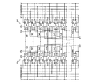
図2は、本発明の第1実施例によるシフトレジスタのブロック図である。図2に示されているように、第1シフトレジスタ400Lは各ゲート線の片側からゲート信号Gout1、Gout2、…を印加し、第2シフトレジスタ400Rは同じゲート線の反対側からゲート信号Gout1、Gout2、…を印加する。第1シフトレジスタ400Lと第2シフトレジスタ400Rとは同時に起動し、同じゲート線に対するゲート信号Gout1、Gout2、…のレベルを同時に切り換える。
FIG. 2 is a block diagram of the shift register according to the first embodiment of the present invention. As shown in FIG. 2, the
第1シフトレジスタ400Lはj個の左側ステージSTL1、…、STL(j)(j≧n)から成り、ゲート信号Gout1、…、Gout(j)のレベルを順番にゲートオン電圧に切り換える。第2シフトレジスタ400Rは、左側ステージと同数、すなわちj個の右側ステージSTR1、…、STR(j)から成り、ゲート信号Gout1、…、Gout(j)のレベルを順番にゲートオン電圧に切り換える。奇数番目の左側ステージSTL1、STL3、STL5、…は縦続接続され、偶数番目の左側ステージSTL2、STL4、STL6、…は縦続接続されている。同様に、奇数番目の右側ステージSTR1、STR3、STR5、…は縦続接続され、偶数番目の右側ステージSTR2、STR4、STR6、…は縦続接続されている。
The
本発明の第1実施例によるシフトレジスタ400L、400Rは構造が同一である。従って、以下、第1シフトレジスタ400Lの構造について説明し、第2シフトレジスタ400Rの構造については第1シフトレジスタ400Lの説明を援用する。
The shift registers 400L and 400R according to the first embodiment of the present invention have the same structure. Therefore, hereinafter, the structure of the
各ステージSTL1、…、STL(j)は、第1クロック端子CK1、第2クロック端子CK2、セット端子S、リセット端子R、オフ電圧端子GV、フレームリセット端子FR、ゲート出力端子OUT1、及びキャリ出力端子OUT2を含む。 Each stage STL1,..., STL (j) has a first clock terminal CK1, a second clock terminal CK2, a set terminal S, a reset terminal R, an off voltage terminal GV, a frame reset terminal FR, a gate output terminal OUT1, and a carry output. Including terminal OUT2.
(4i+1)番目(i=0、1、2、…)のステージSTL1、STL5、…の第1クロック端子CK1には第1クロック信号CKV1が入力され、第2クロック端子CK2には第1反転クロック信号CKVB1が入力される。(4i+2)番目のステージSTL2、STL6、…の第1クロック端子には第2クロック信号CKV2が入力され、第2クロック端子CK2には第2反転クロック信号CKVB2が入力される。(4i+3)番目のステージSTL3、STL7、…の第1クロック端子CK1には第1反転クロック信号CKVB1が入力され、第2クロック端子CK2には第1クロック信号CKV1が入力される。(4i+4)番目のステージSTL4、STL8、…の第1クロック端子には第2反転クロック信号CKVB2が入力され、第2クロック端子CK2には第2クロック信号CKV2が入力される。 The first clock signal CKV1 is input to the first clock terminal CK1 of the (4i + 1) -th (i = 0, 1, 2,...) Stage STL1, STL5,..., And the first inverted clock is input to the second clock terminal CK2. The signal CKVB1 is input. The second clock signal CKV2 is input to the first clock terminal of the (4i + 2) th stage STL2, STL6,..., And the second inverted clock signal CKVB2 is input to the second clock terminal CK2. The first inverted clock signal CKVB1 is input to the first clock terminal CK1 of the (4i + 3) th stage STL3, STL7,..., And the first clock signal CKV1 is input to the second clock terminal CK2. The second inverted clock signal CKVB2 is input to the first clock terminal of the (4i + 4) th stage STL4, STL8,..., And the second clock signal CKV2 is input to the second clock terminal CK2.
図4に、二対のクロック信号CKV1、CKVB1、CKV2、CKVB2の波形を示す。図4に示されているように、各クロック信号の周期Tはいずれも水平周期1Hの4倍に等しい。第1クロック信号CKV1と第1反転クロック信号CKVB1とは互いに逆位相であり、第2クロック信号CKV2と第2反転クロック信号CKVB2とは互いに逆位相である。また、第2クロック信号CKV2は第1クロック信号CKV1より位相が1/4周期、すなわち1水平周期1H遅れている。同様に、第1反転クロック信号CKVB1は第2反転クロック信号CKVB2より位相が1/4周期遅れている。
FIG. 4 shows waveforms of two pairs of clock signals CKV1, CKVB1, CKV2, and CKVB2. As shown in FIG. 4, the period T of each clock signal is equal to four times the
先頭のステージSTL1からn番目のステージSTL(n)までの各ゲート出力端子OUT1は1本のゲート線G1、…、Gnに接続され、そのゲート線に対してゲート信号Gout1、…、Gout(n)を出力する。 Each gate output terminal OUT1 from the first stage STL1 to the nth stage STL (n) is connected to one gate line G1,..., Gn, and gate signals Gout1,. ) Is output.
図4に、先頭から4番目までの各ステージST1、…、STL4から出力されるゲート信号Gout1、…、Gout4の波形を示す。尚、他のステージから出力されるゲート信号の波形も同様である。図4に示されているように、各ゲート信号Gout1、Gout2、…のレベルは、1フレーム当たり水平周期1Hの2倍の時間ずつゲートオン電圧Vonに維持され、それ以外の期間ではゲートオフ電圧Voffに維持される。ゲートオン電圧Vonの持続期間は、好ましくは、予備充電区間と主充電区間との二つに分けられる。更に好ましくは、予備充電区間と主充電区間とは長さが等しく、特に1水平周期1Hに等しい。データ駆動回路500は、各ゲート信号Gout1、Gout2、…の主充電区間M1、M2、…に合わせて、そのゲート信号Gout1、Gout2、…が印加される画素行に対するデータ電圧DATA1、DATA2、…を各データ線D1、D2、…に対して印加する。そのデータ電圧DATA1、DATA2、…によって目標の画素行の各液晶キャパシタが充電され、その両端電圧が目標値に調節される。一方、隣接する二本のゲート線では、前のゲート線によって伝達されるゲート信号、例えば第1ゲート信号Gout1、の主充電区間M1が、後のゲート線によって伝達されるゲート信号、例えば第2ゲート信号Gout2、の予備充電区間P2と重なっている。従って、例えば第2ゲート信号Gout2の予備充電区間P2では、先頭の画素行に対して印加されたデータ電圧DAT1が、第2画素行に対しても印加される。それにより、第2画素行では、各液晶キャパシタが第2ゲート信号Gout2の主充電区間M2に先だって充電を開始する。その結果、その主充電区間M2では、第2画素行の各液晶キャパシタの両端電圧が速やかに、かつ確実に、目標値に到達する。尚、データ駆動回路500は、第1ゲート信号Gout1の予備充電区間P1に合わせて予備のデータ電圧DATA0を各データ線D1、D2、…に対して印加してもよい。それにより、第1ゲート信号Gout1の主充電区間M1では、先頭の画素行の各液晶キャパシタの両端電圧が速やかに、かつ確実に、目標値に到達する。
FIG. 4 shows the waveforms of the gate signals Gout1,..., Gout4 output from the first to fourth stages ST1,. The same applies to the waveforms of gate signals output from other stages. As shown in FIG. 4, the level of each gate signal Gout1, Gout2,... Is maintained at the gate-on voltage Von for a time twice as long as the
第1ステージSTL1のセット端子Sには第1開始信号STV1が入力され、第2ステージSTL2のセット端子Sには第2開始信号STV2が入力される。図4に、各開始信号STV1、STV2の波形を示す。図4に示されているように、各開始信号STV1、STV2のレベルは、各フレームの開始時に水平周期1Hの2倍の時間ずつハイレベルに維持され、それ以外の期間ではローレベルに維持される。更に、第2開始信号STV2の立ち上がりは第1開始信号STV1の立ち上がりより1水平周期1H遅い。第1クロック信号の対CKV1、CKVB1の先頭パルスは第1開始信号STV1に同期して生成され、第2クロック信号の対CKV2、CKVB2の先頭パルスは第2開始信号STV2に同期して生成される。
The first start signal STV1 is input to the set terminal S of the first stage STL1, and the second start signal STV2 is input to the set terminal S of the second stage STL2. FIG. 4 shows waveforms of the start signals STV1 and STV2. As shown in FIG. 4, the levels of the start signals STV1 and STV2 are maintained at a high level at a time twice the
第3ステージSTL3以降の各ステージSTL(i)(i=3、4、…)のセット端子Sには、二つ前のステージSTL(i−2)のキャリ出力端子が接続されている。ここで、各ステージSTL1、…、STL(j)はキャリ出力端子OUT2からキャリ信号を出力する。従って、第3ステージSTL3以降の各ステージSTL(i)のセット端子Sには、二つ前のステージSTL(i−2)からそのキャリ信号が入力される。 The carry output terminal of the previous stage STL (i−2) is connected to the set terminal S of each stage STL (i) (i = 3, 4,...) After the third stage STL3. Here, each stage STL1,..., STL (j) outputs a carry signal from the carry output terminal OUT2. Therefore, the carry signal is input from the previous stage STL (i−2) to the set terminal S of each stage STL (i) after the third stage STL3.
最後の三つのステージSTL(j−2)、STL(j−1)、STL(j)を除く各ステージSTL(i)(i=1、2、…、j−3)のリセット端子Rは、三つ後ろのステージSTL(i+3)のゲート出力端子OUT1に接続され、そこからゲート信号Gout(i+3)を受信する。最後の三つのステージSTL(j−2)〜STL(j)のリセット端子Rには、第1開始信号STV1が入力される。 The reset terminal R of each stage STL (i) (i = 1, 2,..., J−3) excluding the last three stages STL (j−2), STL (j−1), and STL (j) is It is connected to the gate output terminal OUT1 of the next three stages STL (i + 3), and receives the gate signal Gout (i + 3) therefrom. The first start signal STV1 is input to the reset terminals R of the last three stages STL (j−2) to STL (j).
各ステージSTL1、…、STL(j)のオフ電圧端子GVにはゲートオフ信号Voffが入力され、フレームリセット端子FRには初期化信号INTが入力される。好ましくは、各ステージSTL1、…、STL(j)のフレームリセット端子FRは、最後のステージSTL(j)のキャリ出力端子OUT2に接続されている。それにより、最後のステージSTL(j)のキャリ信号が初期化信号INTとして各ステージSTL1、…、STL(j)に供給される。 The gate off signal Voff is input to the off voltage terminal GV of each stage STL1,..., STL (j), and the initialization signal INT is input to the frame reset terminal FR. Preferably, the frame reset terminal FR of each stage STL1,..., STL (j) is connected to the carry output terminal OUT2 of the last stage STL (j). Thereby, the carry signal of the last stage STL (j) is supplied to each stage STL1,..., STL (j) as the initialization signal INT.
最後の三つのステージSTL(j)、STL(j−1)、STL(j−2)は好ましくはダミーステージとして利用される。すなわち、それら三つのステージSTL(j)、STL(j−1)、STL(j−2)の各ゲート出力端子OUT1は、ダミーのゲート線、又は前段の三つのステージSTL(j−3)、STL(j−4)、STL(j−5)の各リセット端子Rに接続される。また、最後の三つのステージSTL(j)、STL(j−1)、STL(j−2)のキャリ出力端子OUT2は、開放されていてもよい。 The last three stages STL (j), STL (j−1), and STL (j−2) are preferably used as dummy stages. That is, the gate output terminals OUT1 of these three stages STL (j), STL (j−1), and STL (j−2) are dummy gate lines, or the preceding three stages STL (j−3), Connected to each reset terminal R of STL (j-4) and STL (j-5). Further, the carry output terminal OUT2 of the last three stages STL (j), STL (j−1), and STL (j−2) may be opened.
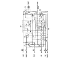
図3は、図2に示されている第1シフトレジスタ400Lの左側ステージSTL(i)(i=1、2、…、j)の等価回路図である。以下、図3を参照しながら、各ステージの等価回路を説明する。尚、第2シフトレジスタ400Rの右側ステージSTR(i)は第1シフトレジスタ400Lの左側ステージSTL(i)と等価回路が同一である。従って、以下、左側ステージSTL(i)の等価回路について説明し、右側ステージの等価回路については左側ステージSTL(i)の説明を援用する。
FIG. 3 is an equivalent circuit diagram of the left stage STL (i) (i = 1, 2,..., J) of the
図3に示されているように、各ステージは、プルアップ駆動部211、プルダウン部219、プルアップ部213、キャリ出力部214、リップル改善部215、インバータ部216、保持部217、リセット部218、及びリップル防止部215aを有する。
As shown in FIG. 3, each stage includes a pull-up
プルアップ駆動部211は、第4スイッチング素子T4、第1キャパシタC1、及び第2キャパシタC2を含む。第4スイッチング素子T4のゲートとソースとはセット端子Sに接続され、ドレインは第1ノードN1に接続されている。第1キャパシタC1は第1ノードN1と第2ノードN2との間に接続されている。第2キャパシタC2は第1ノードN1とキャリ出力端子OUT2との間に接続されている。プルアップ駆動部211は、セット端子Sを通して二つ前のステージSTL(i−2)からキャリ信号Cout(i−2)を受信し、そのキャリ信号Cout(i−2)のレベルに応じてプルアップ部213の第1スイッチング素子T1をオンオフさせる。尚、第1ステージSTL1のセット端子Sには第1開始信号STV1が入力され、第2ステージSTL2のセット端子Sには第2開始信号STV2が入力される。
The pull-up
プルダウン部219は、プルダウンスイッチング素子T2と第9スイッチング素子T9とを含む。プルダウンスイッチング素子T2のゲートはリセット端子Rに接続され、ソースはオフ電圧端子GVに接続され、ドレインはゲート出力端子OUT1に接続されている。第9スイッチング素子T9のゲートはリセット端子Rに接続され、ソースはオフ電圧端子GVに接続され、ドレインは第1ノードN1を通してプルアップ部213の第1スイッチング素子T1のゲートに接続されている。ここで、第9スイッチング素子T9のアスペクト比は、プルアップ部213の第1スイッチング素子T1のアスペクト比の1/20〜1/10に設定されている。
The pull-down
プルダウンスイッチング素子T2は、三つ後ろのステージSTL(i+3)からのゲート信号Gout(i+3)に応じてオンオフすることにより、ゲート出力端子OUT1をオフ電圧端子GVに接続し、又はその接続を遮断する。尚、最後の三つのステージSTL(j−2)〜STL(j)のプルダウンスイッチング素子T2は、第1開始信号STV1に応じてオンオフする。プルダウンスイッチング素子T2は特に、ゲート信号Gout(i+3)の立ち上がりに応じてターンオンし、ゲート出力端子OUT1の電圧、すなわちゲート信号GOUT(i)のレベルをゲートオフ電圧Voffに維持する。一方、第9スイッチング素子T9は、三つ後ろのステージSTL(i+3)からのゲート信号Gout(i+3)に応じてオンオフすることにより、第1スイッチング素子T1のゲートをオフ電圧端子GVに接続し、又はその接続を遮断する。尚、最後の三つのステージSTL(j−2)〜STL(j)の第9スイッチング素子T9は、第1開始信号STV1に応じてオンオフする。第9スイッチング素子T9は特に、ゲート信号Gout(i+3)の立ち上がりに応じてターンオンし、第1スイッチング素子T1のゲート電位をゲートオフ電圧Voffに維持して、第1スイッチング素子T1をターンオフさせる。このように、プルダウン部219は、三つ後ろのステージSTL(i+3)からのゲート信号Gout(i+3)又は第1開始信号STV1の立ち上がりに応じて、ゲート信号Gout(i)のレベルをゲートオフ電圧Voffに維持し、それと同時に、プルアップ部213の第1スイッチング素子T1をターンオフさせる。また、プルダウン部219は第1キャパシタC1の両端を短絡させて、第1キャパシタC1を完全に放電させる。
The pull-down switching element T2 connects or disconnects the gate output terminal OUT1 to the off-voltage terminal GV by turning on and off in accordance with the gate signal Gout (i + 3) from the next three stages STL (i + 3). . Note that the pull-down switching elements T2 of the last three stages STL (j-2) to STL (j) are turned on / off according to the first start signal STV1. In particular, the pull-down switching element T2 is turned on in response to the rise of the gate signal Gout (i + 3), and maintains the voltage of the gate output terminal OUT1, that is, the level of the gate signal GOUT (i) at the gate-off voltage Voff. On the other hand, the ninth switching element T9 is turned on / off according to the gate signal Gout (i + 3) from the three subsequent stages STL (i + 3), thereby connecting the gate of the first switching element T1 to the off-voltage terminal GV. Or block the connection. The ninth switching element T9 of the last three stages STL (j-2) to STL (j) is turned on / off according to the first start signal STV1. In particular, the ninth switching element T9 is turned on in response to the rise of the gate signal Gout (i + 3), maintains the gate potential of the first switching element T1 at the gate-off voltage Voff, and turns off the first switching element T1. In this manner, the pull-down
プルアップ部213は第1スイッチング素子T1を含む。第1スイッチング素子T1のゲートは第1ノードN1に接続され、ソースは第1クロック端子CK1に接続され、ドレインはゲート出力端子OUT1に接続されている。すなわち、第1スイッチング素子T1のドレインがプルアップ部213の出力端子として利用される。第1スイッチング素子T1は、プルアップ駆動回路211から供給されるキャリ信号Cout(i−2)の立ち上がりに応じてターンオンして第1クロック端子CK1をゲート出力端子OUT1に接続する。それにより、第1クロック端子CK1に供給されるクロック信号CKV1(又は、CKVB1、CKV2、CKVB2)をゲート信号Gout(i)としてゲート出力端子OUT1から出力する。プルアップ部213はまた、プルダウン部219から供給されるゲートオフ電圧Voffによってターンオフして、第1クロック端子CK1をゲート出力端子OUT1から分離する。
The pull-up
キャリ出力部214は第15スイッチング素子T15を含む。第15スイッチング素子T15のゲートは第1ノードN1に接続され、ソースは第1クロック端子CK1に接続され、ドレインはキャリ出力端子OUT2に接続されている。キャリ出力部214は、プルアップ駆動回路211に従ってターンオンして第1クロック端子CK1をキャリ出力端子OUT1に接続する。それにより、第1クロック端子CK1を介して供給されるクロック信号CKV1、CKVB1、CKV2、又はCKVB2がキャリ信号Cout(i)としてキャリ出力端子OUT2から出力される。尚、その他の実施例として、キャリ信号Cout(i)は、第15スイッチング素子T15に代えて、プルアップ部213の出力端子から出力されてもよい。その場合、キャリ出力部214は省略されてもよい。
The
リップル改善部215は、第11スイッチング素子T11、第10スイッチング素子T10、及び第5スイッチング素子T5を含む。それらのスイッチング素子T11、T10、T5はその順で、セット端子Sとオフ電圧端子GVとの間に直列に接続されている。第11スイッチング素子T11のゲートは第2クロック端子CK2に接続され、ソースはセット端子Sに接続されて、ドレインは第1ノードN1に接続されている。第10スイッチング素子T10のゲートは第1クロック端子CK1に接続され、ソースは第2ノードN2に接続され、ドレインは第1ノードN1に接続されている。第5スイッチング素子T5のゲートは第2クロック端子CK2に接続され、ソースはオフ電圧端子GVに接続され、ドレインは第2ノードN2に接続されている。
The
第10スイッチング素子T10は、第1クロック端子CK1に供給されるクロック信号CKV1(又は、CKVB1、CKV2、CKVB2)に応じてオンオフし、第1ノードN1と第2ノードN2との間を接続し、又はその接続を遮断する。第10スイッチング素子T10は特に、第1クロック端子CK1の電位がゲート出力端子OUT1の電位より高く上昇したときにターンオンし、第1ノードN1と第2ノードN2とを通してゲート出力端子OUT1を第1スイッチング素子T1のゲートに接続する。それにより、後述のように、ゲート信号Gout(i)から、クロック信号CKV1(又は、CKVB1、CKV2、CKVB2)の立ち上がりに伴うリップルを除去する。 The tenth switching element T10 is turned on / off according to the clock signal CKV1 (or CKVB1, CKV2, CKVB2) supplied to the first clock terminal CK1, and connects between the first node N1 and the second node N2. Or block the connection. The tenth switching element T10 is turned on particularly when the potential of the first clock terminal CK1 rises higher than the potential of the gate output terminal OUT1, and the gate output terminal OUT1 is switched to the first switching through the first node N1 and the second node N2. Connect to the gate of element T1. Thereby, as described later, the ripple accompanying the rise of the clock signal CKV1 (or CKVB1, CKV2, CKVB2) is removed from the gate signal Gout (i).
第11スイッチング素子T11は、第2クロック端子CK2に供給される反転クロック信号CKVB1(又は、CKV1、CKVB2、CKV2)に応じてオンオフし、セット端子Sを第1ノードN1に接続し、又はその接続を遮断する。第11スイッチング素子T11は特に、第2クロック端子CK2の電位が第1ノードN1の電位より高く立ち上がるときにターンオンし、セット端子Sと第1ノードN1とを通して二つ前のステージからのキャリ信号Cout(i−2)を第1スイッチング素子T1のゲートに供給する。それにより、後述のように、ゲート信号Gout(i)から、反転クロック信号CKVB1(又は、CKV1、CKVB2、CKV2)の立ち上がり、すなわち、クロック信号CKV1(又は、CKVB1、CKV2、CKVB2)の立ち下がりに伴うリップルを除去する。 The eleventh switching element T11 is turned on / off according to the inverted clock signal CKVB1 (or CKV1, CKVB2, CKV2) supplied to the second clock terminal CK2, and the set terminal S is connected to the first node N1, or the connection thereof Shut off. The eleventh switching element T11 is turned on particularly when the potential of the second clock terminal CK2 rises higher than the potential of the first node N1, and the carry signal Cout from the previous stage through the set terminal S and the first node N1. (i-2) is supplied to the gate of the first switching element T1. As a result, as described later, from the gate signal Gout (i), the rising edge of the inverted clock signal CKVB1 (or CKV1, CKVB2, CKV2), that is, the falling edge of the clock signal CKV1 (or CKVB1, CKV2, CKVB2). Remove the accompanying ripple.
第5スイッチング素子T5は、第2クロック端子CK2に供給される反転クロック信号CKVB1(又は、CKV1、CKVB2、CKV2)に応じてオンオフし、オフ電圧端子GVを第2ノードN2に接続し、又はその接続を遮断する。第5スイッチング素子T5は特に、第2クロック端子CK2の電位が第1ノードN1の電位より高く立ち上がるときにターンオンし、第2ノードN2を通してゲートオフ電圧Voffをゲート出力端子OUT1に供給する。それにより、後述のように、ゲート信号Gout(i)から、反転クロック信号CKVB1(又は、CKV1、CKVB2、CKV2)の立ち上がり、すなわち、クロック信号CKV1(又は、CKVB1、CKV2、CKVB2)の立ち下がりに伴うリップルを除去する。 The fifth switching element T5 is turned on / off according to the inverted clock signal CKVB1 (or CKV1, CKVB2, CKV2) supplied to the second clock terminal CK2, and connects the off voltage terminal GV to the second node N2, or Disconnect the connection. In particular, the fifth switching element T5 is turned on when the potential of the second clock terminal CK2 rises higher than the potential of the first node N1, and supplies the gate-off voltage Voff to the gate output terminal OUT1 through the second node N2. As a result, as described later, from the gate signal Gout (i), the rising edge of the inverted clock signal CKVB1 (or CKV1, CKVB2, CKV2), that is, the falling edge of the clock signal CKV1 (or CKVB1, CKV2, CKVB2). Remove the accompanying ripple.
インバータ部216は、四個のスイッチング素子T12、T7、T13、T8と二個のキャパシタC3、C4を含む。第12スイッチング素子T12のゲートとソースとは第1クロック端子CK1に接続され、ドレインは第3ノードN3に接続されている。第7スイッチング素子T7のゲートは第3ノードN3に接続され、ソースは第1クロック端子CK1に接続され、ドレインは第4ノードN4に接続されている。第3キャパシタC3は第1クロック端子CK1と第3ノードN3の間に接続され、第4キャパシタC4は第3ノードN3と第4ノードN4の間に接続されている。第13スイッチング素子T13と第8スイッチング素子T8との各ゲートは第5ノードN5に接続され、各ソースはオフ電圧端子GVに接続されている。第13スイッチング素子T13のドレインは第3ノードN3に接続され、第8スイッチング素子T8のドレインは第4ノードN4に接続されている。
The
第12スイッチング素子T12と第7スイッチング素子T7とは、第1クロック端子CK1に供給されるクロック信号CKV1(又は、CKVB1、CKV2、CKVB2)に応じてオンオフし、第1クロック端子CK1を第3ノードN3及び第4ノードN4に接続し、又はその接続を遮断する。第13スイッチング素子T13と第8スイッチング素子T8とは、第5ノードN5の電位に応じて同時にオンオフする。第13スイッチング素子T13はターンオンすることによって第3ノードN3をオフ電圧端子GVに接続し、その電位をゲートオフ電圧Voffに維持する。第8スイッチング素子T8はターンオンすることによって第4ノードN4をオフ電圧端子GVに接続し、その電位をゲートオフ電圧Voffに維持する。 The twelfth switching element T12 and the seventh switching element T7 are turned on / off according to the clock signal CKV1 (or CKVB1, CKV2, CKVB2) supplied to the first clock terminal CK1, and the first clock terminal CK1 is set to the third node. Connect to N3 and the fourth node N4 or cut off the connection. The thirteenth switching element T13 and the eighth switching element T8 are simultaneously turned on / off according to the potential of the fifth node N5. The thirteenth switching element T13 is turned on to connect the third node N3 to the off voltage terminal GV and maintain the potential at the gate off voltage Voff. The eighth switching element T8 is turned on to connect the fourth node N4 to the off-voltage terminal GV and maintain the potential at the gate-off voltage Voff.
保持部217は、第3スイッチング素子T3を含む。第3スイッチング素子T3のゲートはインバータ部216の第4ノードN4に接続され、ソースはオフ電圧端子GVに接続され、ドレインはゲート出力端子OUT1に接続されている。第3スイッチング素子T3は第4ノードN4の電位に応じてオンオフし、オフ電圧端子GVをゲート出力端子OUT1に接続し、又はその接続を遮断する。
The holding
リセット部218は、第6スイッチング素子T6を含む。プルアップ駆動部第6スイッチング素子T6のゲートはフレームリセット端子FRに接続され、ソースはオフ電圧端子GVに接続され、ドレインは第1ノードN1に接続されている。第6スイッチング素子T6は、初期化信号INT、すなわち、最後のステージSTL(j)からのキャリ信号Cout(j)に応じてオンオフし、オフ電圧端子GVを第1ノードN1に接続し、又はその接続を遮断する。第6スイッチング素子T6は特に、後述のように、各フレームの終了時にターンオンすることによって、第1スイッチング素子T1と第15スイッチング素子T15とを確実にターンオフさせて、ゲート出力端子OUT1とキャリ出力端子OUT2とをリセットする。
The
リップル防止部215aは、リップル防止ダイオードRT17、リップル防止スイッチング素子RT18、及びリップル防止キャパシタRC7を含む。リップル防止ダイオードRT17は、好ましくはダイオード接続のスイッチング素子から成る。そのスイッチング素子RT17のソースとゲートとは第2ノードN2に共通接続され、ドレインはインバータ部216の第5ノードN5を通して第8スイッチング素子T8と第13スイッチング素子T13との各ゲートに接続されている。リップル防止スイッチング素子RT18のドレインは第5ノードN5に接続され、ゲートは第2クロック端子CK2に接続され、ソースはオフ電圧端子GVに接続されている。リップル防止キャパシタRC7は第8スイッチング素子T8のゲートとソースとの間に接続されている。尚、リップル防止キャパシタRC7は第13スイッチング素子T13のゲートとソースとの間に接続されていてもよい。
The
ゲート線がその寄生キャパシタを通して外部からノイズを受けた場合、そのノイズの影響により、そのゲート線からゲート出力端子OUT1にリップル信号が入力されることがある。その場合、そのリップル信号は、インバータ部216の第8スイッチング素子T8と第13スイッチング素子T13との各ゲートに、直接ではなく、リップル防止ダイオードRT17を通して入力される。従って、リップル信号に伴う各ゲート電位の急激な上昇は、少なくともリップル防止ダイオードRT17のしきい値電圧だけ弱められるので、インバータ部216の動作、特に第8スイッチング素子T8と第13スイッチング素子T13との動作が、リップル信号の影響を受けにくくなる。
When the gate line receives noise from the outside through the parasitic capacitor, a ripple signal may be input from the gate line to the gate output terminal OUT1 due to the influence of the noise. In that case, the ripple signal is input to each gate of the eighth switching element T8 and the thirteenth switching element T13 of the
リップル防止スイッチング素子RT18は、第2クロック端子CK2に入力される反転クロック信号CKVB1(又は、CKV1、CKVB2、CKV2)に応じてオンオフして、インバータ部216の第8スイッチング素子T8と第13スイッチング素子T13との各ゲートをオフ電圧端子GVに接続し、又はその接続を遮断する。リップル防止スイッチング素子RT18は特に、後述のように、反転クロック信号CKVB1(又は、CKV1、CKVB2、CKV2)の立ち上がりに応じてターンオンし、第8スイッチング素子T8と第13スイッチング素子T13との各ゲート電位をゲートオフ電圧Voffに維持する。それにより、反転クロック信号CKVB1(又は、CKV1、CKVB2、CKV2)の立ち上がり、すなわち、クロック信号CKV1(又は、CKVB1、CKV2、CKVB2)の立ち下がりに伴ってゲート出力端子OUT1から、第2ノードN2とリップル防止ダイオードRT17とを通して第5ノードN5に供給されるリップル信号を、第8スイッチング素子T8と第13スイッチング素子T13との各ゲートから除去する。
The ripple prevention switching element RT18 is turned on / off according to the inverted clock signal CKVB1 (or CKV1, CKVB2, CKV2) input to the second clock terminal CK2, and the eighth switching element T8 and the thirteenth switching element of the
リップル防止キャパシタRC7の一端はオフ電圧端子GVに接続されているので、その電位がゲートオフ電圧Voffに維持されている。従って、ゲート出力端子OUT1から、第2ノードN2とリップル防止ダイオードRT17とを通して第5ノードN5に供給されるリップル信号は、リップル防止キャパシタRC7をバイパスしてオフ電圧端子GVに流れる。それにより、インバータ部216の第8スイッチング素子T8と第13スイッチング素子T13との各ゲートにはリップル信号が流入しないので、各ゲートがリップル信号から保護される。
Since one end of the ripple preventing capacitor RC7 is connected to the off voltage terminal GV, the potential thereof is maintained at the gate off voltage Voff. Accordingly, the ripple signal supplied from the gate output terminal OUT1 to the fifth node N5 through the second node N2 and the ripple prevention diode RT17 bypasses the ripple prevention capacitor RC7 and flows to the off-voltage terminal GV. Thereby, since the ripple signal does not flow into each gate of the eighth switching element T8 and the thirteenth switching element T13 of the
図4は、図2に示されている先頭から4番目までの左側ステージSTL1〜STL4に入出力される信号の波形図である。以下、図2、図3、図4を参照しながら、左側ステージの先頭である第1ステージSTL1の動作を説明する。尚、他のステージSTL2〜STL(j)、STR1〜STR(j)の動作も同様である。 FIG. 4 is a waveform diagram of signals input to and output from the first to fourth left side stages STL1 to STL4 shown in FIG. Hereinafter, the operation of the first stage STL1, which is the head of the left stage, will be described with reference to FIGS. The operations of the other stages STL2 to STL (j) and STR1 to STR (j) are the same.
図4に示されている第1開始信号STV1の立ち上がり時刻t1では、まず、セット端子Sの電位が立ち上がるので、プルアップ駆動回路211の第4スイッチング素子T4がターンオンする。それにより、第1ノードN1の電位がゲートオフ電圧Voffから立ち上がる。一方、第1ステージSTL1のゲート出力端子OUT1、キャリ出力端子OUT2の各電位はいずれも、ゲートオフ電圧Voffに維持されている。従って、ゲート出力端子OUT1と第1ノードN1との間の電位差によって第1キャパシタC1が充電され、キャリ出力端子OUT2と第1ノードN1との間の電位差によって第2キャパシタC2が充電される。尚、リセット部218の第6スイッチング素子が予め、好ましくは直前のフレームの終了時に、フレームリセット端子FRに入力された初期化信号INTの立ち上がりに応じてターンオンして第1キャパシタC1と第2キャパシタC2との各一端をオフ電圧端子GVに接続し、各キャパシタC1、C2を完全に放電させる。その結果、時刻t1では、いずれのキャパシタC1、C2も、電荷を蓄積していない状態から充電を開始する。
At the rise time t1 of the first start signal STV1 shown in FIG. 4, first, the potential of the set terminal S rises, so that the fourth switching element T4 of the pull-up
時刻t1では更に、第1ノードN1での電位上昇により、プルアップ部213の第1スイッチング素子T1がターンオンして第1クロック端子CK1をゲート出力端子OUT1に接続し、キャリ出力部214の第15スイッチング素子T15がターンオンして第1クロック端子CK1をキャリ出力端子OUT2に接続する。そのとき、第1キャパシタC1はその両端電圧を第1スイッチング素子T1のしきい値電圧以上に維持し、第2キャパシタC2はその両端電圧を第15スイッチング素子T15のしきい値電圧以上に維持する。一方、第4ステージSTL4からリセット端子Rに入力されるゲート信号Gout4のレベルはゲートオフ電圧Voffに維持されているので、プルダウン部219のプルダウンスイッチング素子T2と第9スイッチング素子T9とはいずれもオフ状態を維持している。また、時刻t1では、保持部217の第3スイッチング素子T3がオフ状態を維持している。従って、第1クロック端子CK1に供給される第1クロック信号CKV1が、ゲート出力端子OUT1からはゲート信号Gout1として出力され、キャリ出力端子OUT2からはキャリ信号Cout1として出力される。このとき、第1クロック端子CK1では第1クロック信号CKV1が立ち上がるので、ゲート信号Gout1とキャリ信号Cout1との各レベルがゲートオン電圧Vonに上昇する。
At time t1, the first switching element T1 of the pull-up
第1クロック信号CKV1の立ち上がり時、第2クロック端子CK2では、第1反転クロック信号CKVB1が立ち下がる。従って、リップル改善部215では、第10スイッチング素子T10がターンオンし、第11スイッチング素子T11と第5スイッチング素子T5とがターンオフする。第10スイッチング素子T10のターンオンにより、第1ノードN1と第2ノードN2とを通してゲート出力端子OUT1が第1スイッチング素子T1のゲートに接続される。それにより、第1クロック信号CKV1の立ち上がりに伴うゲート出力端子OUT1での急激な電位上昇が第1スイッチング素子T1のゲートにフィードバックされ、第1スイッチング素子T1のドレインとゲートとの間の電位差が安定に維持される。その結果、ゲート信号Gout1から、第1クロック信号CKV1の立ち上がりに伴うリップルが除去される。尚、第10スイッチング素子T10のオン抵抗は十分に高いので、第10スイッチング素子T10を通した各キャパシタC1、C2の放電は十分に遅く、各放電量は十分に小さい。
When the first clock signal CKV1 rises, the first inverted clock signal CKVB1 falls at the second clock terminal CK2. Accordingly, in the
リップル防止部215aでは、第2クロック端子CK2での第1反転クロック信号CKVB1の立ち下がりに応じて、リップル防止スイッチング素子RT18がターンオフする。従って、第1クロック信号CKV1の立ち上がりに伴うゲート出力端子OUT1の電位上昇が、リップル防止ダイオードRT17を通して第5ノードN5の電位を上昇させる。それにより、インバータ部216の第13スイッチング素子T13と第8スイッチング素子T8とがいずれもターンオンする。ここで、第5ノードN5の急激な電位上昇に伴うリップル信号は、リップル防止ダイオードRT17とリップル防止キャパシタRC7を通してオフ電圧端子GVにバイパスされる。更に、第5ノードN5の電位上昇量はゲート出力端子OUT1の電位上昇量より、少なくともリップル防止ダイオードRT17のしきい値電圧だけ小さい。こうして、リップル信号から各スイッチング素子T13、T8のゲートが保護される。
In the
インバータ部216では更に、第1クロック信号CKV1の立ち上がりに応じて第12スイッチング素子T12がターンオンして、第3ノードN3の電位を上昇させる。そのとき、第7スイッチング素子T7が続いてターンオンするように、第12スイッチング素子T12と第13スイッチング素子T13との間でのオン抵抗比は設計されている。従って、第3ノードN3の電位上昇に伴って第4ノードN4の電位が上昇する。更にそのとき、保持部217の第3スイッチング素子T3がオフ状態を維持するように、第7スイッチング素子T7と第8スイッチング素子T8との間でのオン抵抗比は設計されている。
Further, in the
第1クロック信号CKV1の立ち上がりに伴うゲート出力端子OUT1の電位上昇は、第1キャパシタC1を通して第1ノードN1の電位を更に上昇させる。第1ノードN1の電位がセット端子Sの電位、すなわち第1開始信号STV1のハイレベルに達したとき、プルアップ駆動回路211の第4スイッチング素子T4がターンオフするので、第1ノードN1の電位が更に上昇を続ける。その結果、図4に示されているように、時刻t1では、第1ノードN1の電位がゲートオフ電圧Voffから第1電圧レベルV1まで上昇する。更に、時刻t1から水平周期の2倍の時間が経過するまでの期間bでは第1クロック信号CKV1はハイレベルに維持されるので、第1ノードN1の電位は第1電圧レベルV1に維持され、第1スイッチング素子T1はオン状態を維持し、ゲート信号Gout1のレベルはゲートオン電圧Vonに維持される。
The rise in the potential of the gate output terminal OUT1 accompanying the rise of the first clock signal CKV1 further raises the potential of the first node N1 through the first capacitor C1. When the potential of the first node N1 reaches the potential of the set terminal S, that is, the high level of the first start signal STV1, the fourth switching element T4 of the pull-up
第1開始信号STV1の立ち上がり時刻t1から1水平周期1Hが経過した時、第2開始信号STV2が立ち上がる。それにより、第2ステージSTL2では、セット端子S、第1クロック端子CK1の各電位が立ち上がるので、第2ステージSTL2は時刻t1での第1ステージSTL1の動作と同様に動作して、ゲート信号Gout2のレベルをゲートオン電圧Vonに上昇させる。こうして、第1ステージSTL1がゲート信号Gout1をゲートオン電圧Vonに維持する期間の後半の1水平周期1H、すなわち主充電期間M1と、第2ステージSTL2がゲート信号Gout2をゲートオン電圧Vonに維持する期間の前半の1水平周期1H、すなわち予備充電期間P2とが重なる。
When one
第1開始信号STV1の立ち上がり時刻t1から水平周期1Hの2倍が経過するまでの期間bでは、第1ステージSTL1はキャリ信号Cout1をハイレベルに維持する。それにより、第3ステージSTL3では第1ステージSTL1と同様に、セット端子Sの電位の立ち上がりによって第1スイッチング素子T1がターンオンして、第1クロック端子CK1をゲート出力端子OUT1に接続する。しかし、第3ステージSTL3では第1ステージSTL1とは、各クロック端子CK1、CK2に入力されるクロック信号が反対である。すなわち、時刻t1では第1クロック端子CK1の電位は立ち下がり、第2クロック端子CK2の電位が立ち上がる。従って、第3ステージSTL3は第1ステージSTL1とは逆に、ゲート信号Gout3のレベルをゲートオフ電圧Voffに維持する。
In the period b from the rising time t1 of the first start signal STV1 until the double of the
時刻t1から水平周期1Hの2倍の時間が経過した時刻t2では、第1クロック信号CKV1は立ち下がり、第1反転クロック信号CKVB1は立ち上がる。そのとき、第1ステージSTL1では、第1キャパシタC1の両端電圧によって第1スイッチング素子T1がオン状態を維持する一方、プルダウンスイッチング素子T2、第9スイッチング素子T9、及び第3スイッチング素子T3がいずれもオフ状態を維持している。従って、第1クロック端子CK1に供給される第1クロック信号CKV1がゲート出力端子OUT1を通してゲート信号Gout1として出力され続けるので、ゲート信号Gout1がゲートオフ電圧Voffに立ち下がり、主充電期間M1が終了する。尚、第2キャパシタC2の両端電圧によって第15スイッチング素子T15もオン状態を維持しているので、キャリ信号Cout1もゲート信号Gout1と同様に、ゲートオン電圧Voffに立ち下がる。
At time t2 when time twice as long as the
時刻t2では更に、ゲート出力端子OUT1の電位降下に伴い、第1ノードN1の電位は、図4に示されているように、第1電圧レベルV1より低い第2電圧レベルV2に降下する。ここで、第2電圧レベルV2はゲートオフ電圧Voffより第1キャパシタC1の両端電圧だけ高いので、第1ノードN1とゲート出力端子OUT1との間の電位差は第1スイッチング素子T1のしきい値電圧以上である。従って、第1ノードN1の電位が第2電圧レベルV2に維持される期間では、第1スイッチング素子T1はオン状態を維持する。 At time t2, the potential of the first node N1 further drops to the second voltage level V2 lower than the first voltage level V1, as shown in FIG. 4, with the potential drop of the gate output terminal OUT1. Here, since the second voltage level V2 is higher than the gate-off voltage Voff by the voltage across the first capacitor C1, the potential difference between the first node N1 and the gate output terminal OUT1 is greater than or equal to the threshold voltage of the first switching element T1. It is. Accordingly, the first switching element T1 maintains the on state during the period in which the potential of the first node N1 is maintained at the second voltage level V2.
時刻t2では、第2クロック端子CK2に供給される第1反転クロック信号CKVB1が立ち下がるので、リップル改善部215では、第10スイッチング素子T10がターンオフし、第11スイッチング素子T11と第5スイッチング素子T5とがターンオンする。第11スイッチング素子T11のターンオンにより、セット端子Sと第1ノードN1とを通して第1開始信号STV1の立ち下がりが第1スイッチング素子T1のゲートに伝わる。一方、第5スイッチング素子T5のターンオンにより、第2ノードN2を通してゲートオフ電圧Voffがゲート出力端子OUT1に供給される。それらにより、第1クロック信号CKV1の立ち下がりに伴うゲート出力端子OUT1での急激な電位降下に関わらず、第1スイッチング素子T1のドレインとゲートとの間の電位差が安定に維持される。その結果、ゲート信号Gout1から、第1クロック信号CKV1の立ち下がりに伴うリップルが除去される。尚、第11スイッチング素子T11と第5スイッチング素子T5との各オン抵抗は十分に高いので、各スイッチング素子T11、T5を通した各キャパシタC1、C2の放電は十分に遅く、各放電量は十分に小さい。従って、時刻t2から、リセット端子Rに供給される第4ステージSTL4のゲート信号Gout4の次に立ち上がる時刻t3までの期間cにおいて、第1ノードN1の電位は第2電圧レベルV2に維持される。
At time t2, the first inverted clock signal CKVB1 supplied to the second clock terminal CK2 falls, and therefore, in the
リップル防止部215aでは、第2クロック端子CK2での第1反転クロック信号CKVB1の立ち上がりに応じてリップル防止スイッチング素子RT18がターンオンし、オフ電圧端子GVを第5ノードN5に接続する。従って、第5ノードN5の電位がゲートオフ電圧Voffに維持されるので、インバータ部216の第13スイッチング素子T13と第8スイッチング素子T8とがいずれもターンオフする。ここで、第1クロック信号CKV1の立ち下がりに伴ってゲート出力端子OUT1から、第2ノードN2とリップル防止ダイオードRT17とを通して第5ノードN5に供給されるリップル信号は、リップル防止スイッチング素子RT18を通してオフ電圧端子GVにバイパスされるので、リップル信号から各スイッチング素子T8、T13のゲートが保護される。
In the
インバータ部216では更に、第1クロック信号CKV1の立ち下がりに応じて第12スイッチング素子T12がターンオフし、第3キャパシタC3を通して第3ノードN3の電位が降下する。従って、第7スイッチング素子T7が続いてターンオフし、第4キャパシタC4を通して第4ノードN4の電位が降下する。その結果、保持部217の第3スイッチング素子T3がオフ状態を維持する。
Further, in the
時刻t2から1水平周期1H後の時刻t3では、図4に示されているように、第4ステージSTL4がそのゲート信号Gout4のレベルをゲートオン電圧Vonに上昇させるので、第1ステージSTL1ではリセット端子Rの電位が立ち上がる。従って、第9スイッチング素子T9がターンオンして、オフ電圧端子GVを第1ノードN1に接続するので、第1ノードN1の電位は、第2電圧レベルV2からゲートオフ電圧Voffに降下する。更にそのとき、第1キャパシタC1及び第2キャパシタC2は、第9スイッチング素子T9を通して放電する。それにより、第1スイッチング素子T1及び第15スイッチング素子T15がいずれもターンオフする。
At time t3, which is one
尚、他の実施例として、時刻t3では、プルダウンスイッチング素子T2に代えて、第9スイッチング素子T9によって、オフ電圧端子GVがゲート出力端子OUT1に接続されてもよい。比較的広いスペースが必要であるプルダウンスイッチング素子T2を除去することにより、液晶パネル300内においてゲート駆動回路400L、400Rの占める空間を縮小した場合、ゲート駆動回路400L、400Rの工程マージン、すなわち、位置決め時における許容誤差を十分な大きさに確保できる。
As another example, at time t3, the off-voltage terminal GV may be connected to the gate output terminal OUT1 by the ninth switching element T9 instead of the pull-down switching element T2. When the space occupied by the
時刻t3以後、次のフレームまでの期間dでは、第1ノードN1の電位がゲートオフ電圧Voffに維持されるので、第1スイッチング素子T1がオフ状態を維持する。従って、第1反転クロック信号CKVB1のハイレベル期間では、ゲート出力端子OUT1の電位がリップル防止ダイオードRT17及びリップル防止スイッチング素子RT18を通してオフ電圧端子GVの電位、すなわちゲートオフ電圧Voffに維持される。そのとき、インバータ部216の第13スイッチング素子T13と第8スイッチング素子T8とがオフ状態を維持する。一方、第1クロック信号CKV1のハイレベル期間では、インバータ部216の第12スイッチング素子T12と第7スイッチング素子T7とがターンオンするので、第4ノードN4の電位が上昇する。そのとき、第8スイッチング素子T8はオフ状態を維持しているので、保持部217の第3スイッチング素子T3がターンオンし、オフ電圧端子GVをゲート出力端子OUT1に接続する。それにより、ゲート出力端子OUT1の電位はゲートオフ電圧Voffに維持される。更に第5ノードN5の電位がリップル防止ダイオードRT17を通してゲートオフ電圧Voffに維持されるので、第13スイッチング素子T13と第8スイッチング素子T8とはオフ状態に維持される。こうして、ゲート出力端子OUT1の電位、すなわちゲート信号Gout1のレベルは、時刻t3以降、ゲートオフ電圧Voffに安定に維持される。
After time t3, in the period d until the next frame, the potential of the first node N1 is maintained at the gate-off voltage Voff, so that the first switching element T1 is maintained in the off state. Therefore, during the high level period of the first inverted clock signal CKVB1, the potential of the gate output terminal OUT1 is maintained at the potential of the off-voltage terminal GV, that is, the gate-off voltage Voff through the ripple prevention diode RT17 and the ripple prevention switching element RT18. At that time, the thirteenth switching element T13 and the eighth switching element T8 of the
以上のとおり、第1実施例による液晶表示装置では、外部からのノイズによって各ゲート線からゲート駆動回路400L、400Rのゲート出力端子OUT1に入力されるリップル信号、及び、各ステージがゲート信号Gout1、…、Gout(j)のレベルを変動させるときにゲート出力端子OUT1に生じ得るリップル信号から、リップル防止部215aがインバータ部216の第8スイッチング素子T8と第13スイッチング素子T13との各ゲートを保護する。それにより、リップル信号に起因するインバータ部216と保持部217との出力不良を防止することができる。その結果、各ステージは、自身の出力するゲート信号の歪みを低減できる。更に、各ステージは三つ後ろのステージからリセット端子Rに入力されるゲート信号を利用するので、一つのステージにおけるゲート信号の歪みの低減は、他のステージにおけるゲート信号の歪みの低減にも寄与する。その結果、すべてのステージでゲート信号の歪みが低減する。こうして、本発明の第1実施例によるゲート駆動回路400L、400Rはその信頼性を更に向上させ、液晶表示装置の画質を更に向上させることができる。
As described above, in the liquid crystal display device according to the first embodiment, the ripple signal input from each gate line to the gate output terminal OUT1 of the
図5は、本発明の第2実施例による第1シフトレジスタ400Lの左側ステージSTL(i)(i=1、2、…、j)の等価回路図である。以下、図5を参照しながら、各ステージの等価回路を説明する。尚、第2シフトレジスタ400Rの右側ステージSTR(i)は第1シフトレジスタ400Lの左側ステージSTL(i)と等価回路が同一である。従って、以下、左側ステージSTL(i)の等価回路について説明し、右側ステージの等価回路については左側ステージSTL(i)の説明を援用する。
FIG. 5 is an equivalent circuit diagram of the left stage STL (i) (i = 1, 2,..., J) of the
図5に示されているように、各ステージは、プルアップ駆動部211、プルダウン部219、プルアップ部213、キャリ出力部214、リップル改善部215、インバータ部216、保持部217、リセット部218、及び、リップル防止部215bを含む。本発明の第2実施例によるステージは、図3に示されている第1実施例によるステージと比べ、リップル防止部215bが異なる。その他の部分は本発明の第1実施例による部分と同様であるので、その説明については、第1実施例についての説明を援用する。
As shown in FIG. 5, each stage includes a pull-up
本発明の第2実施例におけるリップル防止部215bは、リップル防止ダイオードRT17、リップル防止スイッチング素子RT18、及びリップル防止キャパシタRC7を含む。リップル防止ダイオードRT17は、好ましくはダイオード接続のスイッチング素子から成る。そのスイッチング素子RT17のソースとゲートとは、ゲート出力端子OUT1に代えて、キャリ出力端子OUT2に共通接続され、ドレインはインバータ部216の第5ノードN5を通して第8スイッチング素子T8と第13スイッチング素子T13との各ゲートに接続されている。リップル防止スイッチング素子RT18とリップル防止キャパシタRC7とは、第1実施例によるものと同様に接続されている。
The ripple prevention unit 215b in the second embodiment of the present invention includes a ripple prevention diode RT17, a ripple prevention switching element RT18, and a ripple prevention capacitor RC7. The ripple preventing diode RT17 is preferably formed of a diode-connected switching element. The source and gate of the switching element RT17 are connected in common to the carry output terminal OUT2 instead of the gate output terminal OUT1, and the drains are connected to the eighth switching element T8 and the thirteenth switching element T13 through the fifth node N5 of the
第5ノードN5はゲート出力端子OUT1及びゲート線からは分離されているので、ゲート信号の変動に伴うリップル信号がインバータ部216には悪影響を与えない。一方、キャリ出力端子OUT2にリップル信号が発生した場合、そのリップル信号は、インバータ部216の第8スイッチング素子T8と第13スイッチング素子T13との各ゲートに、直接ではなく、リップル防止ダイオードRT17を通して入力される。従って、リップル信号に伴う各ゲート電位の急激な上昇は、少なくともリップル防止ダイオードRT17のしきい値電圧だけ弱められるので、インバータ部216の動作、特に第8スイッチング素子T8と第13スイッチング素子T13との動作が、リップル信号の影響を受けにくくなる。
Since the fifth node N5 is separated from the gate output terminal OUT1 and the gate line, the ripple signal accompanying the fluctuation of the gate signal does not adversely affect the
リップル防止スイッチング素子RT18は、反転クロック信号CKVB1(又は、CKV1、CKVB2、CKV2)の立ち上がり、すなわち、クロック信号CKV1(又は、CKVB1、CKV2、CKVB2)の立ち下がりに伴ってキャリ出力端子OUT2からリップル防止ダイオードRT17を通して第5ノードN5に供給されるリップル信号を、第8スイッチング素子T8と第13スイッチング素子T13との各ゲートから除去する。 The ripple prevention switching element RT18 prevents ripple from the carry output terminal OUT2 when the inverted clock signal CKVB1 (or CKV1, CKVB2, CKV2) rises, that is, when the clock signal CKV1 (or CKVB1, CKV2, CKVB2) falls. The ripple signal supplied to the fifth node N5 through the diode RT17 is removed from the gates of the eighth switching element T8 and the thirteenth switching element T13.
リップル防止キャパシタRC7は、キャリ出力端子OUT2からリップル防止ダイオードRT17を通して第5ノードN5に供給されるリップル信号をオフ電圧端子GVにバイパスさせる。それにより、インバータ部216の第8スイッチング素子T8と第13スイッチング素子T13との各ゲートにはリップル信号が流入しないので、各ゲートがリップル信号から保護される。
The ripple prevention capacitor RC7 bypasses the ripple signal supplied from the carry output terminal OUT2 to the fifth node N5 through the ripple prevention diode RT17 to the off-voltage terminal GV. Thereby, since the ripple signal does not flow into each gate of the eighth switching element T8 and the thirteenth switching element T13 of the
第2実施例による液晶表示装置では、インバータ部216がゲート出力端子OUT1から分離されているので、インバータ部216は、ゲート出力端子OUT1に入力されるリップル信号には影響されない。一方、外部からのノイズによってゲート駆動回路400L、400Rのキャリ出力端子OUT2に入力されるリップル信号、及び、各ステージがキャリ信号Cout1、…、Cout(j)のレベルを変動させるときにキャリ出力端子OUT2に生じ得るリップル信号から、リップル防止部215bがインバータ部216の第8スイッチング素子T8と第13スイッチング素子T13との各ゲートを保護する。それにより、リップル信号に起因するインバータ部216と保持部217との出力不良を防止することができる。その結果、各ステージは、自身の出力するゲート信号の歪みを低減できる。更に、各ステージは三つ後ろのステージからリセット端子Rに入力されるゲート信号を利用するので、一つのステージにおけるゲート信号の歪みの低減は、他のステージにおけるゲート信号の歪みの低減にも寄与する。その結果、すべてのステージでゲート信号の歪みが低減する。こうして、本発明の第2実施例によるゲート駆動回路400L、400Rはその信頼性を更に向上させ、液晶表示装置の画質を更に向上させることができる。
In the liquid crystal display device according to the second embodiment, since the
図6は、本発明の第3実施例による第1シフトレジスタ400Lの左側ステージSTL(i)(i=1、2、…、j)の等価回路図である。以下、図6を参照しながら、各ステージの等価回路を説明する。尚、第2シフトレジスタ400Rの右側ステージSTR(i)は第1シフトレジスタ400Lの左側ステージSTL(i)と等価回路が同一である。従って、以下、左側ステージSTL(i)の等価回路について説明し、右側ステージの等価回路については左側ステージSTL(i)の説明を援用する。
FIG. 6 is an equivalent circuit diagram of the left stage STL (i) (i = 1, 2,..., J) of the
図6に示されているように、各ステージは、プルアップ駆動部211、プルダウン部219、プルアップ部213、キャリ出力部214、リップル改善部215、インバータ部216、保持部217、リセット部218、リップル防止部215c、及び第2プルアップ部RT19を含む。本発明の第3実施例によるステージは、図3に示されている第1実施例によるステージと比べ、リップル防止部215cと第2プルアップ部RT19とが異なる。その他の部分は本発明の第1実施例による部分と同様であるので、その説明については、第1実施例についての説明を援用する。
As shown in FIG. 6, each stage includes a pull-up
本発明の第3実施例におけるリップル防止部215cは、リップル防止ダイオードRT17、リップル防止スイッチング素子RT18、及びリップル防止キャパシタRC7を含む。リップル防止ダイオードRT17は、好ましくはダイオード接続のスイッチング素子から成る。そのスイッチング素子RT17のソースとゲートとは、ゲート出力端子OUT1に代えて、第2プルアップ部RT19の出力端子に共通接続され、ドレインはインバータ部216の第5ノードN5を通して第8スイッチング素子T8と第13スイッチング素子T13との各ゲートに接続されている。リップル防止スイッチング素子RT18とリップル防止キャパシタRC7とは、第1実施例によるものと同様に接続されている。
The
第2プルアップ部RT19は、好ましくはスイッチング素子であり、そのゲートはプルアップ部213の第1スイッチング素子T1のゲートに接続され、ソースは第1スイッチング素子T1のソースに接続され、ドレインはリップル防止ダイオードRT17のアノード、すなわちスイッチング素子RT17のゲートとソースとに接続されている。
The second pull-up part RT19 is preferably a switching element, and its gate is connected to the gate of the first switching element T1 of the pull-up
第2プルアップ部RT19は第1スイッチング素子T1と同じタイミングでオンオフし、第1クロック端子CK1をリップル防止ダイオードRT17のアノードに接続し、又はその接続を遮断する。それにより、リップル防止部215c及びインバータ部216の第8スイッチング素子T8と第13スイッチング素子T13とを、第1実施例によるものと同様に動作させることができる。一方、第3実施例では、インバータ部216の第8スイッチング素子T8と第13スイッチング素子T13との各ゲートが、リップル防止ダイオードRT17、第2プルアップ部RT19、及び第1スイッチング素子T1を通してゲート出力端子OUT1に接続されている。従って、ゲート信号の変動に伴うリップル信号がそれらのゲートに直に入力することを防止できる。また、第2プルアップ部RT19で発生するリップル信号は、リップル防止ダイオードRT17によって弱められ、又は、リップル防止スイッチング素子RT18若しくはリップル防止キャパシタRC7を通してオフ電圧端子GVにバイパスされる。それにより、リップル信号がインバータ部216に与える悪影響が防止される。
The second pull-up unit RT19 is turned on / off at the same timing as the first switching element T1, and the first clock terminal CK1 is connected to the anode of the ripple prevention diode RT17 or is disconnected. Accordingly, the eighth switching element T8 and the thirteenth switching element T13 of the
以上のとおり、第3実施例による液晶表示装置では、外部からのノイズによってゲート駆動回路400L、400Rのゲート出力端子OUT1に入力されるリップル信号、及び、各ステージがゲート信号Gout1、…、Gout(j)のレベルを変動させるときにゲート出力端子OUT1に生じ得るリップル信号から、第2プルアップ部RT19及びリップル防止部215cがインバータ部216の第8スイッチング素子T8と第13スイッチング素子T13との各ゲートを保護する。それにより、リップル信号に起因するインバータ部216と保持部217との出力不良を防止することができる。その結果、各ステージは、自身の出力するゲート信号の歪みを低減できる。更に、各ステージは三つ後ろのステージからリセット端子Rに入力されるゲート信号を利用するので、一つのステージにおけるゲート信号の歪みの低減は、他のステージにおけるゲート信号の歪みの低減にも寄与する。その結果、すべてのステージでゲート信号の歪みが低減する。こうして、本発明の第3実施例によるゲート駆動回路400L、400Rはその信頼性を更に向上させ、液晶表示装置の画質を更に向上させることができる。
As described above, in the liquid crystal display device according to the third embodiment, the ripple signal input to the gate output terminal OUT1 of the
本発明の各実施例によるゲート駆動回路400L、400Rは、各ステージSTL、STRのインバータ部216と出力端子OUT1、OUT2との間に、ダイオードRT17、スイッチング素子RT18、及びキャパシタRC7の少なくとも1つを設けている。それにより、各ステージの出力信号、特にゲート信号Gout(i)のレベル変動に伴ってインバータ部216に入力されるリップル信号を弱め、又はオフ電圧端子GVにバイパスさせる。その結果、そのリップル信号がインバータ部216に及ぼす悪影響を除去することができる。その結果、ゲート駆動回路400L、400Rの信頼性を更に向上させることができる。
The
尚、本発明の実施形態は上述の実施例には限られず、本発明の技術的範囲から逸脱しない範囲内で、各実施例を多様に変更することが可能である。 The embodiments of the present invention are not limited to the above-described embodiments, and various embodiments can be variously modified without departing from the technical scope of the present invention.
211…プルアップ駆動部
219…プルダウン部
213…プルアップ部
214…キャリ出力部
215…リップル改善部
215a、215b、215c…リップル防止部
216…インバータ部
RT19…第2プルアップ部
217…保持部
218…リセット部
300…液晶パネル
400L…第1シフトレジスタ
400R…第2シフトレジスタ
500…データ駆動回路
600…タイミング制御部
700…電圧生成部
800…階調電圧生成部
211 ... Pull-up drive
219 ... Pull-down section
213 ... Pull-up part
214 ... Carry output section
215… Ripple improvement department
215a, 215b, 215c ... Ripple prevention part
216… Inverter part
RT19 ... 2nd pull-up part
217 ... Holding part
218 ... Reset section
300 ... LCD panel
400L ... 1st shift register
400R ... Second shift register
500 ... Data drive circuit
600 ... Timing control unit
700… Voltage generator
800 ... gradation voltage generator
Claims (9)
各ステージは、
クロック信号を受信し、ゲート信号を前記クロック信号に合わせて変動させるプルアップ部、
前記プルアップ部に接続され、前段のステージのいずれかからキャリ信号を受信し、前記キャリ信号に応じて前記プルアップ部を動作させるプルアップ駆動部、
後段のステージのいずれかからゲート信号を受信して、そのゲート信号に応じて前記プルアップ部にゲート信号のレベルをゲートオフ電圧まで降下させるプルダウン部、
ゲート信号のレベルをゲートオフ電圧に維持する保持部、
前記クロック信号に応じて前記保持部を動作させるインバータ部、及び、
前記インバータ部の入力端子に入力されるリップル信号を弱め、又はバイパスさせるリップル防止部、
を含み、
前記リップル防止部は、
互いに直接連結されているソースとゲートとが前記プルアップ部の出力端子に共通接続され、ドレインが前記インバータ部の入力端子に接続されているスイッチング素子から成るリップル防止ダイオードを有する、ゲート駆動回路。 A gate drive circuit including a plurality of stages connected in cascade,
Each stage
A pull-up unit for receiving a clock signal and changing a gate signal in accordance with the clock signal;
A pull-up driving unit that is connected to the pull-up unit, receives a carry signal from any one of the preceding stages, and operates the pull-up unit according to the carry signal;
A pull-down unit that receives a gate signal from any one of the subsequent stages and drops the level of the gate signal to the gate-off voltage in the pull-up unit according to the gate signal;
A holding unit for maintaining the level of the gate signal at the gate-off voltage;
An inverter for operating the holding unit in response to the clock signal; and
A ripple prevention unit that weakens or bypasses the ripple signal input to the input terminal of the inverter unit,
Only including,
The ripple prevention unit is
A gate driving circuit comprising a ripple prevention diode comprising a switching element in which a source and a gate directly connected to each other are commonly connected to an output terminal of the pull-up unit and a drain is connected to an input terminal of the inverter unit .
ドレインが前記リップル防止ダイオードのドレインに接続され、ソースの電位がゲートオフ電圧に維持され、ゲートが前記クロック信号の反転信号を受信するリップル防止スイッチング素子、
を更に有する、請求項1に記載のゲート駆動回路。 The ripple prevention unit is
An anti-ripple switching element having a drain connected to the drain of the anti-ripple diode, a source potential maintained at a gate-off voltage, and a gate receiving an inverted signal of the clock signal;
Further comprising a gate driving circuit according to claim 1.
を更に有する、請求項3に記載のゲート駆動回路。 A second pull-up unit that receives the clock signal through an input terminal connected to an input terminal of the pull-up unit and varies an output signal according to the clock signal;
The gate drive circuit according to claim 3 , further comprising:
ドレインが前記クロック信号を受信し、ソースの電位がゲートオフ電圧に維持され、ゲートが前記リップル防止ダイオードのドレインに接続されている一対のスイッチング素子、
を含み、
前記リップル防止部は、
前記一対のスイッチング素子のいずれかのゲートとソースとの間に接続されているリップル防止キャパシタ、
を含む、請求項1に記載のゲート駆動回路。 The inverter unit is
A pair of switching elements, wherein the drain receives the clock signal, the potential of the source is maintained at a gate-off voltage, and the gate is connected to the drain of the anti-ripple diode;
Including
The ripple prevention unit is
An anti-ripple capacitor connected between the gate and source of any of the pair of switching elements;
The gate drive circuit according to claim 1 , comprising:
Applications Claiming Priority (2)
| Application Number | Priority Date | Filing Date | Title |
|---|---|---|---|
| KR10-2007-0078578 | 2007-08-06 | ||
| KR1020070078578A KR101415562B1 (en) | 2007-08-06 | 2007-08-06 | Gate driving circuit and display apparatus having the same |
Publications (3)
| Publication Number | Publication Date |
|---|---|
| JP2009054273A JP2009054273A (en) | 2009-03-12 |
| JP2009054273A5 JP2009054273A5 (en) | 2011-07-28 |
| JP5512104B2 true JP5512104B2 (en) | 2014-06-04 |
Family
ID=40346021
Family Applications (1)
| Application Number | Title | Priority Date | Filing Date |
|---|---|---|---|
| JP2008200994A Active JP5512104B2 (en) | 2007-08-06 | 2008-08-04 | Gate drive circuit and display device having the same |
Country Status (4)
| Country | Link |
|---|---|
| US (2) | US8305326B2 (en) |
| JP (1) | JP5512104B2 (en) |
| KR (1) | KR101415562B1 (en) |
| CN (1) | CN101364392B (en) |
Families Citing this family (58)
| Publication number | Priority date | Publication date | Assignee | Title |
|---|---|---|---|---|
| KR101471553B1 (en) * | 2008-08-14 | 2014-12-10 | 삼성디스플레이 주식회사 | Gate driving circuit and display device having the same |
| TWI402814B (en) * | 2009-01-16 | 2013-07-21 | Chunghwa Picture Tubes Ltd | Gate driving circuit capable of suppressing threshold voltage drift |
| TWI406247B (en) * | 2009-05-04 | 2013-08-21 | Au Optronics Corp | Common-voltage compensation circuit and compensation method for use in a liquid crystal display |
| TWI436321B (en) * | 2009-06-25 | 2014-05-01 | Innolux Corp | Image display system |
| US8766960B2 (en) * | 2009-06-25 | 2014-07-01 | Innolux Corporation | Image display system |
| US8803784B2 (en) * | 2009-07-15 | 2014-08-12 | Sharp Kabushiki Kaisha | Scanning signal line drive circuit and display device having the same |
| KR101587610B1 (en) * | 2009-09-21 | 2016-01-25 | 삼성디스플레이 주식회사 | Driving circuit |
| KR102005736B1 (en) | 2009-10-16 | 2019-07-31 | 가부시키가이샤 한도오따이 에네루기 켄큐쇼 | Manufacturing method of semiconductor device |
| KR20110049560A (en) * | 2009-11-05 | 2011-05-12 | 삼성전자주식회사 | Display device |
| KR101641312B1 (en) * | 2009-12-18 | 2016-07-21 | 삼성디스플레이 주식회사 | Display panel |
| KR101094286B1 (en) * | 2010-05-10 | 2011-12-19 | 삼성모바일디스플레이주식회사 | Emission driver, light emitting display device using the same, and driving method of emission control signals |
| KR101641721B1 (en) * | 2010-06-24 | 2016-07-25 | 삼성디스플레이 주식회사 | Driving circuit for display device |
| KR101479297B1 (en) * | 2010-09-14 | 2015-01-05 | 삼성디스플레이 주식회사 | Scan driver and organic light emitting display using the same |
| KR101719187B1 (en) * | 2010-09-14 | 2017-03-24 | 삼성디스플레이 주식회사 | Emission driver and organic light emitting display using the same |
| KR101868528B1 (en) | 2011-07-05 | 2018-06-20 | 삼성디스플레이 주식회사 | Display panel |
| CN102629459A (en) * | 2011-10-26 | 2012-08-08 | 北京京东方光电科技有限公司 | Gate line driving method, shift register and gate line driving device |
| KR102005485B1 (en) * | 2011-11-04 | 2019-07-31 | 삼성디스플레이 주식회사 | Display panel |
| TWI436332B (en) * | 2011-11-30 | 2014-05-01 | Au Optronics Corp | Display panel and gate driver therein |
| CN102629461A (en) * | 2012-02-21 | 2012-08-08 | 北京京东方光电科技有限公司 | Shift register, array substrate driving circuit and display apparatus |
| CN103680427A (en) * | 2012-09-07 | 2014-03-26 | 瀚宇彩晶股份有限公司 | Liquid crystal display and shift registering device thereof |
| KR102034140B1 (en) * | 2013-01-23 | 2019-10-21 | 삼성디스플레이 주식회사 | Gate driver and display device comprising the same |
| CN103310755B (en) * | 2013-07-03 | 2016-01-13 | 深圳市华星光电技术有限公司 | Array base palte horizontal drive circuit |
| US9171516B2 (en) | 2013-07-03 | 2015-10-27 | Shenzhen China Star Optoelectronics Technology Co., Ltd | Gate driver on array circuit |
| CN103714780B (en) | 2013-12-24 | 2015-07-15 | 京东方科技集团股份有限公司 | Grid driving circuit, grid driving method, array substrate row driving circuit and display device |
| CN103730089B (en) | 2013-12-26 | 2015-11-25 | 京东方科技集团股份有限公司 | Gate driver circuit, method, array base palte horizontal drive circuit and display device |
| CN103730094B (en) * | 2013-12-30 | 2016-02-24 | 深圳市华星光电技术有限公司 | Goa circuit structure |
| CN103714781B (en) | 2013-12-30 | 2016-03-30 | 京东方科技集团股份有限公司 | Gate driver circuit, method, array base palte horizontal drive circuit and display device |
| KR102128579B1 (en) * | 2014-01-21 | 2020-07-01 | 삼성디스플레이 주식회사 | Gate driver and display apparatus having the same |
| KR102174888B1 (en) * | 2014-02-12 | 2020-11-06 | 삼성디스플레이 주식회사 | Gate driving circuit and display device having the same |
| CN103839510A (en) * | 2014-03-26 | 2014-06-04 | 华映视讯(吴江)有限公司 | Gate driving circuit |
| CN104036745B (en) | 2014-06-07 | 2017-01-18 | 深圳市华星光电技术有限公司 | Drive circuit and liquid crystal display device |
| KR102315888B1 (en) * | 2014-06-09 | 2021-10-21 | 삼성디스플레이 주식회사 | Gate circuit and display device using the same |
| KR20150142708A (en) * | 2014-06-10 | 2015-12-23 | 삼성디스플레이 주식회사 | A gate driving circuit and a display device having the same |
| KR102314447B1 (en) * | 2015-01-16 | 2021-10-20 | 삼성디스플레이 주식회사 | Gate driving cicuit and display apparatus having them |
| KR102278385B1 (en) * | 2015-01-19 | 2021-07-19 | 삼성디스플레이 주식회사 | Scanline driver |
| KR102281237B1 (en) * | 2015-02-13 | 2021-07-26 | 삼성디스플레이 주식회사 | Gate circuit, driving metohd for gate circuit and display device using the same |
| KR102281753B1 (en) * | 2015-04-14 | 2021-07-27 | 삼성디스플레이 주식회사 | Stage circuit and scan driver using the same |
| CN104835442B (en) * | 2015-05-28 | 2017-09-26 | 京东方科技集团股份有限公司 | Shift register and its driving method, gate driving circuit and display device |
| KR102383363B1 (en) * | 2015-10-16 | 2022-04-07 | 삼성디스플레이 주식회사 | Gate driver and display device having the same |
| CN105355175B (en) * | 2015-11-24 | 2018-06-22 | 深圳市华星光电技术有限公司 | Liquid crystal display drive circuit and gate driving panel |
| CN105374331B (en) * | 2015-12-01 | 2017-11-17 | 武汉华星光电技术有限公司 | Gate driving circuit and the display using gate driving circuit |
| CN205595037U (en) * | 2016-05-13 | 2016-09-21 | 合肥鑫晟光电科技有限公司 | Shifting register, grid driving circuit and display device |
| KR102569931B1 (en) * | 2016-07-13 | 2023-08-25 | 삼성디스플레이 주식회사 | Stage and Display Device Using The Same |
| CN106448599B (en) * | 2016-10-25 | 2019-11-19 | 南京华东电子信息科技股份有限公司 | Forward and reverse scanning gate driving circuit |
| CN106652933B (en) * | 2016-11-18 | 2021-02-26 | 南京中电熊猫液晶显示科技有限公司 | Grid drive circuit with forward and reverse scanning function |
| CN106710510A (en) * | 2017-02-23 | 2017-05-24 | 合肥京东方光电科技有限公司 | Grid driving unit and driving method, grid driving circuit and display device |
| KR102555779B1 (en) * | 2018-02-26 | 2023-07-17 | 삼성디스플레이 주식회사 | Gate driver and display device having the same |
| CN110444138B (en) * | 2018-05-03 | 2023-04-11 | 瀚宇彩晶股份有限公司 | Grid driving circuit and display panel |
| CN108922488B (en) | 2018-08-31 | 2020-05-12 | 重庆惠科金渝光电科技有限公司 | Array substrate, display panel and display device |
| CN108877726B (en) * | 2018-09-04 | 2020-10-02 | 合肥鑫晟光电科技有限公司 | Display driving circuit, control method thereof and display device |
| CN111696490A (en) * | 2019-03-15 | 2020-09-22 | 合肥鑫晟光电科技有限公司 | Shifting register unit and driving method thereof, grid driving circuit and display device |
| TWI714289B (en) * | 2019-10-02 | 2020-12-21 | 友達光電股份有限公司 | Gate driving apparatus |
| CN111028798B (en) | 2019-12-05 | 2021-03-23 | 深圳市华星光电半导体显示技术有限公司 | GOA circuit |
| CN111312188A (en) * | 2020-03-31 | 2020-06-19 | 深圳市华星光电半导体显示技术有限公司 | GOA circuit and display device |
| CN111415624B (en) * | 2020-04-29 | 2021-05-14 | 京东方科技集团股份有限公司 | Shift register circuit and driving method thereof, gate drive circuit and display device |
| CN112233622B (en) * | 2020-10-22 | 2022-04-05 | 深圳市华星光电半导体显示技术有限公司 | GOA circuit and display panel |
| CN114945969B (en) * | 2020-10-23 | 2023-04-18 | 京东方科技集团股份有限公司 | Shift register unit, driving method, driving circuit and display device |
| KR20230009228A (en) * | 2021-07-08 | 2023-01-17 | 엘지디스플레이 주식회사 | Inverter circuit, gate driver using the same ane sensing method display device |
Family Cites Families (11)
| Publication number | Priority date | Publication date | Assignee | Title |
|---|---|---|---|---|
| JPS60170306A (en) * | 1984-02-15 | 1985-09-03 | Hitachi Ltd | Power source noise inverting amplifier circuit |
| EP1517439A1 (en) * | 2003-09-16 | 2005-03-23 | STMicroelectronics S.r.l. | Transistor amplifier |
| KR20050079718A (en) | 2004-02-06 | 2005-08-11 | 삼성전자주식회사 | Shift register and display apparatus including the same |
| JP2005251348A (en) * | 2004-03-08 | 2005-09-15 | Casio Comput Co Ltd | Shift register circuit and its driving control method |
| KR101026807B1 (en) * | 2004-06-09 | 2011-04-04 | 삼성전자주식회사 | Driving apparatus for display device and display panel |
| TWI382264B (en) * | 2004-07-27 | 2013-01-11 | Samsung Display Co Ltd | Thin film transistor array panel and display device including the same |
| KR101014172B1 (en) | 2004-09-13 | 2011-02-14 | 삼성전자주식회사 | Driving unit and display apparatus having the same |
| KR101056369B1 (en) * | 2004-09-18 | 2011-08-11 | 삼성전자주식회사 | Drive unit and display device having same |
| US7430268B2 (en) * | 2006-01-05 | 2008-09-30 | Au Optronics Corporation | Dynamic shift register with built-in disable circuit |
| JP5128102B2 (en) * | 2006-02-23 | 2013-01-23 | 三菱電機株式会社 | Shift register circuit and image display apparatus including the same |
| JP2007317288A (en) * | 2006-05-25 | 2007-12-06 | Mitsubishi Electric Corp | Shift register circuit and image display equipped therewith |
-
2007
- 2007-08-06 KR KR1020070078578A patent/KR101415562B1/en active IP Right Grant
-
2008
- 2008-07-11 CN CN2008101303453A patent/CN101364392B/en active Active
- 2008-07-18 US US12/218,814 patent/US8305326B2/en active Active
- 2008-08-04 JP JP2008200994A patent/JP5512104B2/en active Active
-
2012
- 2012-11-05 US US13/669,364 patent/US8704748B2/en active Active
Also Published As
| Publication number | Publication date |
|---|---|
| US20130063331A1 (en) | 2013-03-14 |
| US8305326B2 (en) | 2012-11-06 |
| US20090040203A1 (en) | 2009-02-12 |
| KR20090014540A (en) | 2009-02-11 |
| CN101364392B (en) | 2012-12-19 |
| US8704748B2 (en) | 2014-04-22 |
| KR101415562B1 (en) | 2014-07-07 |
| CN101364392A (en) | 2009-02-11 |
| JP2009054273A (en) | 2009-03-12 |
Similar Documents
| Publication | Publication Date | Title |
|---|---|---|
| JP5512104B2 (en) | Gate drive circuit and display device having the same | |
| KR101307414B1 (en) | Gate driving circuit and liquid crystal display having the same | |
| JP5229788B2 (en) | Display device driving device and display device including the same | |
| JP5110680B2 (en) | Shift register and display device having the same | |
| US8259895B2 (en) | Bidirectional shifter register and method of driving same | |
| KR101396942B1 (en) | Gate driving unit and liquid crystal display device comprising the same | |
| JP5483517B2 (en) | Liquid crystal display | |
| US20100315403A1 (en) | Display device, method for driving the display device, and scan signal line driving circuit | |
| JP2007317288A (en) | Shift register circuit and image display equipped therewith | |
| JP2008310317A (en) | Drive unit for liquid crystal display, and liquid crystal display containing the same | |
| KR20100071387A (en) | Gate driver | |
| JP2009015291A (en) | Display device and driving method thereof | |
| JP2007034311A (en) | Scan driving apparatus for display device, display device including same, and driving method of display device | |
| JP2008251094A (en) | Shift register circuit and image display apparatus with the same | |
| US20130335665A1 (en) | Integrated gate driver circuit and liquid crystal panel | |
| KR20090009586A (en) | Display apparaturs and method for driving the same | |
| KR101182323B1 (en) | A shifter register | |
| JP5631145B2 (en) | Gate signal line driving circuit and display device | |
| KR101351386B1 (en) | A liquid crystal display device and a method for driving the same | |
| KR101192760B1 (en) | A shift register and a method for driving the same | |
| KR101319322B1 (en) | A liquid crystal display device | |
| KR20080020063A (en) | Shift resister | |
| KR101232171B1 (en) | A shift register | |
| KR101232147B1 (en) | A liquid crystal display device and a method for driving the same | |
| KR20100074933A (en) | Shift register |
Legal Events
| Date | Code | Title | Description |
|---|---|---|---|
| A521 | Request for written amendment filed |
Free format text: JAPANESE INTERMEDIATE CODE: A523 Effective date: 20110608 |
|
| A621 | Written request for application examination |
Free format text: JAPANESE INTERMEDIATE CODE: A621 Effective date: 20110608 |
|
| RD02 | Notification of acceptance of power of attorney |
Free format text: JAPANESE INTERMEDIATE CODE: A7422 Effective date: 20110608 |
|
| A521 | Request for written amendment filed |
Free format text: JAPANESE INTERMEDIATE CODE: A523 Effective date: 20120508 |
|
| A711 | Notification of change in applicant |
Free format text: JAPANESE INTERMEDIATE CODE: A712 Effective date: 20121213 |
|
| A521 | Request for written amendment filed |
Free format text: JAPANESE INTERMEDIATE CODE: A523 Effective date: 20130322 |
|
| A977 | Report on retrieval |
Free format text: JAPANESE INTERMEDIATE CODE: A971007 Effective date: 20130830 |
|
| A131 | Notification of reasons for refusal |
Free format text: JAPANESE INTERMEDIATE CODE: A131 Effective date: 20130903 |
|
| A521 | Request for written amendment filed |
Free format text: JAPANESE INTERMEDIATE CODE: A523 Effective date: 20131024 |
|
| TRDD | Decision of grant or rejection written | ||
| A01 | Written decision to grant a patent or to grant a registration (utility model) |
Free format text: JAPANESE INTERMEDIATE CODE: A01 Effective date: 20140318 |
|
| A61 | First payment of annual fees (during grant procedure) |
Free format text: JAPANESE INTERMEDIATE CODE: A61 Effective date: 20140326 |
|
| R150 | Certificate of patent or registration of utility model |
Ref document number: 5512104 Country of ref document: JP Free format text: JAPANESE INTERMEDIATE CODE: R150 |
|
| R250 | Receipt of annual fees |
Free format text: JAPANESE INTERMEDIATE CODE: R250 |
|
| R250 | Receipt of annual fees |
Free format text: JAPANESE INTERMEDIATE CODE: R250 |
|
| R250 | Receipt of annual fees |
Free format text: JAPANESE INTERMEDIATE CODE: R250 |
|
| R250 | Receipt of annual fees |
Free format text: JAPANESE INTERMEDIATE CODE: R250 |
|
| R250 | Receipt of annual fees |
Free format text: JAPANESE INTERMEDIATE CODE: R250 |
|
| R250 | Receipt of annual fees |
Free format text: JAPANESE INTERMEDIATE CODE: R250 |
|
| R250 | Receipt of annual fees |
Free format text: JAPANESE INTERMEDIATE CODE: R250 |