JP5476315B2 - Optical assembly, array of optical devices, multi-energy imaging system and method - Google Patents
Optical assembly, array of optical devices, multi-energy imaging system and method Download PDFInfo
- Publication number
- JP5476315B2 JP5476315B2 JP2010537025A JP2010537025A JP5476315B2 JP 5476315 B2 JP5476315 B2 JP 5476315B2 JP 2010537025 A JP2010537025 A JP 2010537025A JP 2010537025 A JP2010537025 A JP 2010537025A JP 5476315 B2 JP5476315 B2 JP 5476315B2
- Authority
- JP
- Japan
- Prior art keywords
- optical
- ray
- energy
- optical device
- optical system
- Prior art date
- Legal status (The legal status is an assumption and is not a legal conclusion. Google has not performed a legal analysis and makes no representation as to the accuracy of the status listed.)
- Expired - Fee Related
Links
Images


Classifications
-
- G—PHYSICS
- G21—NUCLEAR PHYSICS; NUCLEAR ENGINEERING
- G21K—TECHNIQUES FOR HANDLING PARTICLES OR IONISING RADIATION NOT OTHERWISE PROVIDED FOR; IRRADIATION DEVICES; GAMMA RAY OR X-RAY MICROSCOPES
- G21K1/00—Arrangements for handling particles or ionising radiation, e.g. focusing or moderating
- G21K1/06—Arrangements for handling particles or ionising radiation, e.g. focusing or moderating using diffraction, refraction or reflection, e.g. monochromators
- G21K1/062—Devices having a multilayer structure
-
- B—PERFORMING OPERATIONS; TRANSPORTING
- B82—NANOTECHNOLOGY
- B82Y—SPECIFIC USES OR APPLICATIONS OF NANOSTRUCTURES; MEASUREMENT OR ANALYSIS OF NANOSTRUCTURES; MANUFACTURE OR TREATMENT OF NANOSTRUCTURES
- B82Y10/00—Nanotechnology for information processing, storage or transmission, e.g. quantum computing or single electron logic
-
- G—PHYSICS
- G21—NUCLEAR PHYSICS; NUCLEAR ENGINEERING
- G21K—TECHNIQUES FOR HANDLING PARTICLES OR IONISING RADIATION NOT OTHERWISE PROVIDED FOR; IRRADIATION DEVICES; GAMMA RAY OR X-RAY MICROSCOPES
- G21K1/00—Arrangements for handling particles or ionising radiation, e.g. focusing or moderating
- G21K1/10—Scattering devices; Absorbing devices; Ionising radiation filters
-
- H—ELECTRICITY
- H01—ELECTRIC ELEMENTS
- H01J—ELECTRIC DISCHARGE TUBES OR DISCHARGE LAMPS
- H01J35/00—X-ray tubes
- H01J35/02—Details
- H01J35/16—Vessels; Containers; Shields associated therewith
-
- G—PHYSICS
- G21—NUCLEAR PHYSICS; NUCLEAR ENGINEERING
- G21K—TECHNIQUES FOR HANDLING PARTICLES OR IONISING RADIATION NOT OTHERWISE PROVIDED FOR; IRRADIATION DEVICES; GAMMA RAY OR X-RAY MICROSCOPES
- G21K2201/00—Arrangements for handling radiation or particles
- G21K2201/06—Arrangements for handling radiation or particles using diffractive, refractive or reflecting elements
- G21K2201/061—Arrangements for handling radiation or particles using diffractive, refractive or reflecting elements characterised by a multilayer structure
-
- G—PHYSICS
- G21—NUCLEAR PHYSICS; NUCLEAR ENGINEERING
- G21K—TECHNIQUES FOR HANDLING PARTICLES OR IONISING RADIATION NOT OTHERWISE PROVIDED FOR; IRRADIATION DEVICES; GAMMA RAY OR X-RAY MICROSCOPES
- G21K2201/00—Arrangements for handling radiation or particles
- G21K2201/06—Arrangements for handling radiation or particles using diffractive, refractive or reflecting elements
- G21K2201/064—Arrangements for handling radiation or particles using diffractive, refractive or reflecting elements having a curved surface
-
- G—PHYSICS
- G21—NUCLEAR PHYSICS; NUCLEAR ENGINEERING
- G21K—TECHNIQUES FOR HANDLING PARTICLES OR IONISING RADIATION NOT OTHERWISE PROVIDED FOR; IRRADIATION DEVICES; GAMMA RAY OR X-RAY MICROSCOPES
- G21K2201/00—Arrangements for handling radiation or particles
- G21K2201/06—Arrangements for handling radiation or particles using diffractive, refractive or reflecting elements
- G21K2201/067—Construction details
-
- H—ELECTRICITY
- H01—ELECTRIC ELEMENTS
- H01J—ELECTRIC DISCHARGE TUBES OR DISCHARGE LAMPS
- H01J2235/00—X-ray tubes
- H01J2235/18—Windows, e.g. for X-ray transmission
- H01J2235/183—Multi-layer structures
Description
本発明は一般的には、光学技術に関し、さらに具体的には、多層光学装置及び多層光学装置を製造する方法に関する。 The present invention relates generally to optical technology, and more specifically to multilayer optical devices and methods of manufacturing multilayer optical devices.
集束した電磁放射線ビームを必要とする多くの方法が存在する。例えば、爆発性危険物又は他の密輸品の検出のために預かり航空手荷物を検査するのにエネルギ分散性X線回折法(EDXRD)を用いることができる。かかるEDXRDシステムは、回折後のX線信号が弱いため偽陽性率が高くなる場合がある。X線信号が弱いのは多様な原因に起因し得る。第一に、EDXRDに用いられる多色性X線スペクトルは線源スペクトルの制動放射部分によって発生されるため、本質的に強度が低い。第二に、X線源コリメーションのため線源X線の99.99%超が排除されて、解析されている手荷物容積に入射する。第三に、探索されている物質の幾つか、例えば爆発物は、非晶質であるため回折が強くない場合がある。第四に、回折容積が小さい場合がある。最後の二つの制限は手荷物内で探索されている危険物の形式に由来するものであり、このため第二の制限以外の全ての制限は不可避となる。爆発物検出の状況について議論しているが、上述の制限は医療環境にも同等に当てはまる。 There are many methods that require a focused electromagnetic radiation beam. For example, energy dispersive X-ray diffraction (EDXRD) can be used to inspect checked baggage for the detection of explosive hazards or other contraband. Such an EDXRD system may have a high false positive rate because the X-ray signal after diffraction is weak. The weak X-ray signal can be attributed to various causes. First, the polychromatic X-ray spectrum used for EDXRD is inherently low in intensity because it is generated by the bremsstrahlung portion of the source spectrum. Second, because of X-ray source collimation, more than 99.99% of the source X-rays are eliminated and enter the baggage volume being analyzed. Third, some of the materials being sought, such as explosives, may be non-diffractive due to being amorphous. Fourth, the diffraction volume may be small. The last two restrictions are derived from the type of dangerous goods being searched for in the baggage, so all restrictions other than the second restriction are unavoidable. While the explosives detection situation is discussed, the above limitations apply equally to the medical environment.
80keV以下等のような低X線エネルギでは、検査されている物質での多色性X線束密度を高めるために、中空ガラス製ポリキャピラリ光学系を低出力密封管型(静止アノード型)X線源と結合している。中空ガラス製ポリキャピラリ光学系の一例は、例えば米国特許第5,192,869号に記載されている。ガラスは低屈折率物質であり、中空部分を満たしている空気は高屈折率物質である。これらの形式の光学系は典型的には、80keVを上回るエネルギ・レベルでは大きな利得を与えない。というのは、エネルギ・レベルが80keVに近付いてこれを超えると、空気の屈折率とガラスの屈折率との間の差が次第に小さくなるからである。 At low X-ray energies, such as 80 keV or less, a hollow glass polycapillary optical system is used as a low-power sealed tube (static anode) X-ray to increase the polychromatic X-ray flux density in the material being examined. Combined with the source. An example of a hollow glass polycapillary optical system is described, for example, in US Pat. No. 5,192,869. Glass is a low refractive index material, and air filling the hollow portion is a high refractive index material. These types of optics typically do not provide significant gain at energy levels above 80 keV. This is because as the energy level approaches and exceeds 80 keV, the difference between the refractive index of air and the refractive index of the glass becomes progressively smaller.
さらに、かかる光学系は全反射の概念を用いて、適当な角度で中空ガラス製キャピラリに入射したX線を反射して中空キャピラリに戻し、これにより一定立体角の線源X線を通過させて光学系の出力においてコリメートされた又は集束したビームを得ている。本書で用いられる「コリメート」との用語は、本質的に発散性の電磁(EM)ビームからEM放射線ビームの発散を変化させることを指す。典型的には、EM線源の立体角の僅か約5%のみが、かかる公知の光学系の入力によって捕捉される。 Furthermore, such an optical system uses the concept of total reflection to reflect X-rays incident on the hollow glass capillary at an appropriate angle and return them to the hollow capillary, thereby allowing the X-ray source having a certain solid angle to pass through. A collimated or focused beam is obtained at the output of the optical system. As used herein, the term “collimate” refers to changing the divergence of an EM radiation beam from an essentially divergent electromagnetic (EM) beam. Typically, only about 5% of the solid angle of the EM source is captured by the input of such known optics.
加えて、公知の光学系では物質の一つとして空気を用いるので、かかる光学系を真空内に配置することができない。このため、公知の光学系は用途の可能性が限定される。 In addition, since known optical systems use air as one of the materials, such optical systems cannot be placed in a vacuum. For this reason, the possibilities of using known optical systems are limited.
特定の応用向けに最適化するためのX線スペクトルの成形は、広く用いられている手順である。スペクトル形状の変化、例えば低エネルギX線の相対比又は高エネルギX線の相対比の何れかを小さくすると、幾つかの場合に最適な標本の撮像を提供することができる。放射線撮像及び断層写真法撮像に広く見受けられる一つのアーティファクトは、典型的な制動放射(多色性)スペクトルの低エネルギX線が、ビームが物質に進入透過するにつれて優先的に減弱されるとの事実から発生する。この効果は、ビームが標本に進入透過するにつれてビームの平均エネルギの増大を招き、透過したビームの強さと進入透過させられた物質の量との間の関係に偏りを齎す。この偏りは、計算機式断層写真法におけるビーム・ハードニングを原因とするアーティファクト等のように、減弱データから再構成されるあらゆる画像にアーティファクトとして現われる。エネルギの広がり方が小さいX線ビームを用いると、これらのアーティファクトの幾分かを軽減することができる。具体的には、ビーム強度が元のスペクトルの同じ範囲の強度に関して一定に保たれ又は光学系の利用によって増強されている場合には、限定された範囲のエネルギを利用することにより、特定の応用に望ましい減弱の程度を与えることができ、また空間分解能及びコントラスト感度について最適な画像を形成することができる。多色性エネルギ分布からより単色性の分布へのスペクトルの成形はX線画像集合のかかる改善を可能にすることができる。 Shaping the X-ray spectrum to optimize for a specific application is a widely used procedure. Reducing spectral shape changes, such as either the low energy x-ray relative ratio or the high energy x-ray relative ratio, can provide optimal specimen imaging in some cases. One artifact commonly found in radiography and tomography imaging is that low energy x-rays in the typical bremsstrahlung (polychromatic) spectrum are preferentially attenuated as the beam enters and penetrates the material. Arise from the facts. This effect leads to an increase in the average energy of the beam as it enters and penetrates the specimen, biasing the relationship between the intensity of the transmitted beam and the amount of material that has been penetrated and transmitted. This bias appears as an artifact in any image reconstructed from attenuated data, such as artifacts caused by beam hardening in computed tomography. Some of these artifacts can be mitigated by using an X-ray beam with a small energy spread. Specifically, if the beam intensity is kept constant with respect to the intensity of the same range of the original spectrum or is enhanced by the use of an optical system, a limited application of energy can be used for a particular application. The desired degree of attenuation can be provided, and an image optimal for spatial resolution and contrast sensitivity can be formed. Shaping the spectrum from a pleochroic energy distribution to a more monochromatic distribution can allow such an improvement of the x-ray image set.
スペクトル撮像はまた、単一エネルギ分布及び多重エネルギ分布を含んでいる。多重エネルギX線撮像は、二重エネルギ撮像又はエネルギ弁別撮像とも呼ばれ、警備応用、産業応用及び医療応用について走査対象内の特定の物質組成の情報を与えることが実証されている。かかるエネルギ弁別撮像は、しばしば最も現実的なアプローチである2種以上の異なるX線スペクトルの利用等を含めて、多くの方法で行なうことができる。問題は、かかる検査の性質が逐次的であることにあり、例えば画像データは先ず一つのスペクトルを用いて生成され、次いでもう一つのスペクトルを用いて生成される。一つの手法では、関心対象が2回走査される。第一の完全投影データ集合が一つのエネルギにおいて1回目の走査で生成され、次いで第二の完全投影データ集合が第二のエネルギにおいて2回目の走査で生成される。高いスループットが緊要となる多くの応用では、標本組成が動的であり、且つ/又は標本配置が反復的走査を排除する場合があるため、対象を物理的に2回走査するという物資管理手法は許容され得ない。 Spectral imaging also includes single energy distribution and multiple energy distribution. Multi-energy x-ray imaging, also referred to as dual energy imaging or energy discrimination imaging, has been demonstrated to provide information on specific material compositions within a scanned object for security, industrial and medical applications. Such energy discrimination imaging can be performed in many ways, including the use of two or more different X-ray spectra, which is often the most realistic approach. The problem is that the nature of such an examination is sequential, for example, image data is first generated using one spectrum and then using another spectrum. In one approach, the object of interest is scanned twice. A first complete projection data set is generated in the first scan at one energy, and then a second complete projection data set is generated in the second scan at the second energy. In many applications where high throughput is critical, the material management technique of physically scanning the object twice is because the sample composition is dynamic and / or the sample placement may eliminate repetitive scanning. Unacceptable.
従来の多重エネルギX線撮像応用は、線源フィルタ及び/又は高電圧変調を用いて、典型的なCT走査での逐次ビュー式サンプリング時間に匹敵する時間尺度でスペクトル特性を高速変化させている。かかるフィルタは、適当な組成のフィルタを高速に相次いで挿入して、相対的に低いX線エネルギを優先的に減弱させることから成っている。かかる方法論は、減弱が明確に分離したエネルギ間隔を生成し得る程度について限定されており、異なる物質を解析するこのアプローチの感度を厳しく制限している。幾つかの場合に、異なるスペクトル特性を発生する高電圧変調も具現化されているが、限定された成功を得るに留まっている。相異なるエネルギにおいて取得されたデータ集合同士の間の標本移動に起因する画像再構成投影における位置合わせの差、及びX線ビームをサブビュー単位で変調させることにより蒙る対象を横断するX線経路の僅かな位置揃え不正を軽減するアプローチは、何れも困難である。 Conventional multi-energy x-ray imaging applications use source filters and / or high voltage modulation to rapidly change spectral characteristics on a time scale comparable to sequential view sampling time in typical CT scans. Such a filter consists of successively inserting filters of appropriate composition one after the other to preferentially attenuate relatively low x-ray energy. Such methodologies are limited in the extent to which attenuation can produce clearly separated energy intervals and severely limit the sensitivity of this approach to analyzing different materials. In some cases, high voltage modulation that produces different spectral characteristics has also been implemented, but with limited success. Differences in registration in image reconstruction projection due to sample movement between data sets acquired at different energies, and a small amount of X-ray path traversing the object experienced by modulating the X-ray beam in sub-view units Any approach that mitigates misalignment is difficult.
本発明は、光学装置及びフィルタリング機構を含む光学アセンブリに関する実施形態を含んでいる。光学装置は、全反射、回折及び屈折の少なくとも一つを通じて所望の範囲のX線エネルギを透過させる。光学装置は、少なくとも3層の共形(conformal)固相層を含んでおり、固相層同士の間の界面が無間隙であり、少なくとも3層の共形固相層は少なくとも一つのX線方向変更領域を含んでいる。フィルタ機構は光学装置によって透過させられたビームから幾つかのエネルギをフィルタ除去する。フィルタリング機構は、光学装置に対して外部に設けられているフィルタリング装置及び光学装置に一体化されているフィルタリング装置の少なくとも一方である。 The invention includes embodiments that relate to an optical assembly that includes an optical device and a filtering mechanism. The optical device transmits a desired range of x-ray energy through at least one of total reflection, diffraction and refraction. The optical device includes at least three conformal solid phase layers, the interface between the solid phase layers is non-gap, and the at least three conformal solid phase layers are at least one X-ray layer. Includes a direction change area. The filter mechanism filters out some energy from the beam transmitted by the optical device. The filtering mechanism is at least one of a filtering device provided outside the optical device and a filtering device integrated with the optical device.
本発明は、高X線エネルギ又は高低X線エネルギを透過させる第一の光学的部分と、低X線エネルギを透過させる第二の光学的部分とを含む光学装置のアレイに関する実施形態を含んでいる。 The invention includes embodiments that relate to an array of optical devices that includes a first optical portion that transmits high or low X-ray energy and a second optical portion that transmits low X-ray energy. Yes.
本発明は、高エネルギ及び低エネルギ・スペクトル画像から低エネルギ・スペクトル画像を減算することにより高エネルギ・スペクトル画像を形成する方法に関する実施形態を含んでいる。この方法は、全反射、回折及び屈折の少なくとも一つを用いて光学装置を通して高低X線エネルギを透過させるステップを含んでいる。この方法はまた、フィルタリング機構を用いて高エネルギ・スペクトル画像を形成するために光学装置によって透過させられたビームから幾つかのエネルギをフィルタ除去するステップを含んでおり、フィルタリング機構は、光学装置に対して外部に設けられているフィルタリング装置及び光学装置に一体化されているフィルタリング装置の少なくとも一方である。 The present invention includes embodiments that relate to a method for forming a high energy spectral image by subtracting a low energy spectral image from a high energy and low energy spectral image. The method includes transmitting high and low x-ray energy through the optical device using at least one of total reflection, diffraction and refraction. The method also includes filtering some energy from the beam transmitted by the optical device to form a high energy spectral image using the filtering mechanism, the filtering mechanism being applied to the optical device. On the other hand, it is at least one of a filtering device provided outside and a filtering device integrated with the optical device.
本発明は、電子発生源と、電子発生源からの電子によって衝突されるとX線を形成するターゲットと、ターゲットを収容した真空室と、X線が真空室から出るときに通る窓とを含む多重エネルギ・イメージング・システムに関する実施形態を含んでいる。このシステムはまた、所望の範囲のX線エネルギを透過させるように構成されている少なくとも一つの光学装置を含んでいる。 The present invention includes an electron generation source, a target that forms X-rays when struck by electrons from the electron generation source, a vacuum chamber containing the target, and a window through which the X-ray exits the vacuum chamber. Embodiments relating to multi-energy imaging systems are included. The system also includes at least one optical device configured to transmit a desired range of x-ray energy.
本発明は、イメージング・システムにおいて高エネルギX線から低エネルギX線をフィルタ除去する多重エネルギ・イメージング・システムを製造する方法に関する実施形態を含んでいる。この方法は、電子ビームによって衝突されるとX線を形成するように構成されているターゲットを設けるステップと、ターゲットと光学的に連絡している少なくとも一つの光学装置を設けるステップとを含んでいる。少なくとも一つの光学装置は、高X線エネルギを透過させる又は低X線エネルギを透過させるように形成されている。 The present invention includes embodiments that relate to a method of manufacturing a multiple energy imaging system that filters low energy X-rays from high energy X-rays in an imaging system. The method includes providing a target configured to form x-rays when struck by an electron beam and providing at least one optical device in optical communication with the target. . At least one optical device is configured to transmit high x-ray energy or to transmit low x-ray energy.
これらの利点及び特徴、並びに他の利点及び特徴は、添付図面に関連して掲げられている発明の好適実施形態からさらに十分に理解されよう。 These and other advantages and features will be more fully understood from the preferred embodiments of the invention as listed in connection with the accompanying drawings.
本書に記載される発明の各実施形態は主に、全反射の現象を利用する。図1を参照して述べると、入射角が臨界角θcよりも小さいときに全反射が発生する。全反射の臨界角θcは、特に物質の選択、各物質の間の相対的な屈折率の差、物質のフォトン吸収特性、及び入射フォトンのエネルギに依存する。本書に記載される多層光学系の適当な物質選択によって、臨界角θcを空気−ガラス臨界角よりも数倍増大させて、さらに多くのフォトンが全反射の条件を満たすのを可能にすることができる。このことにより、例えばポリキャピラリ光学系について可能であるものよりもさらに大きい多層光学系のフォトン透過が可能になる。 Each of the embodiments of the invention described herein primarily utilizes the phenomenon of total internal reflection. Referring now to FIG. 1, the total reflection occurs when the incident angle is smaller than the critical angle theta c. The critical angle θ c of total reflection depends in particular on the choice of material, the relative refractive index difference between the materials, the photon absorption properties of the material, and the energy of the incident photons. By suitable material selection of the multilayer optical system described herein, a critical angle theta c air - that is increased several times than the glass critical angle, more photons to allow satisfy the condition of total reflection Can do. This allows for photon transmission through a multilayer optical system that is even greater than is possible with, for example, a polycapillary optical system.
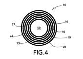
図2〜図5を参照して述べると、入力面12及び出力面14を含む多層光学系10が示されている。「多層」とは、各々の層が単一の組成を有するような複数の層を有する構造を意味する。図3及び図4にさらに具体的に示すように、多層光学系10は多数の層を成す物質を含んでおり、各々の層が異なる屈折率を有する。例えば、芯50を包囲して層16、20及び24が存在している。層15は低屈折率物質で形成されており、芯50の半径方向外部に配置されて、芯50に接している。芯50は高屈折率物質で形成されていてよく、これらの物質はベリリウム、水素化リチウム、マグネシウム、又は同様に高屈折率及び高X線透過特性を有するその他任意の適当な元素若しくは化合物等である。芯50は1マイクロメートルよりも小さい径から1センチメートルよりも大きい径にまでわたっていてよい。層20は、層16の半径方向外部で層24の半径方向内部に配置されている。
Referring to FIGS. 2-5, a multilayer
一実施形態では、多層光学系10を構成する各層は、変化する屈折率を有する複数の物質で形成されていてよい。例えば層15、19、23及び27は、低屈折率及び高X線吸収を有する物質で形成され得る。例えばオスミウム、白金、金、又は同様に低屈折率及び高X線吸収特性を有するその他任意の適当な元素若しくは化合物から適当な物質を選択することができる。さらに、芯50及び層16、20及び24は、高屈折率及び高X線透過性を有する物質で形成され得る。例えばベリリウム、水素化リチウム、マグネシウム、又は同様に高屈折率及び高X線透過特性を有するその他任意の適当な元素若しくは化合物から適当な物質を選択することができる。芯50の径は、光学系の入力面に対するX線放射線源焦点の位置、及び芯50の高屈折率と層15の低屈折率との間の全反射に要求される臨界角を考慮することにより算出される。
In one embodiment, each layer constituting the multilayer
連続した各層において高いX線吸収特性及び低いX線吸収特性をそれぞれ伴って交互に並んだ低屈折率物質及び高屈折率物質を用いることにより、多層光学系10は電磁放射線の全反射の原理を利用することができる。明確に述べると、電磁放射線源34から発する発散性電磁放射線ビーム38、40及び42が入力面12に入り、全反射の原理によって方向変更されて準平行フォトン・ビーム44となり、出力面14から出る。
By using a low-refractive index material and a high-refractive index material alternately arranged with high X-ray absorption characteristics and low X-ray absorption characteristics in each successive layer, the multilayer
本発明の各実施形態による光学系10のような多層光学系は、大きい立体角を成すX線源34を収集し、多色性エネルギを含むフォトンを方向変更して準平行フォトン・ビームとすることができる。「準平行」とは、X線のような発散性フォトン・ビームが収集されて集束させられて電磁放射線ビーム又はX線ビームとなり、臨界角θc以下の角度で出力面14を出ることを意味する。この発散は、本来の線源X線ビームを光学系10の出力面14よりも大きくし、またこの光学系によって発生されるX線の平行ビームよりも大きくする。代替的には、本発明の各実施形態による多層光学系は、僅かに集束したビーム、大きく集束したビーム、僅かに発散したビーム、又は大きく発散したビームを発生するように構成されることもできる。「僅かに集束した」とは、注目される点(すなわちビームの径が問題となる位置)でのビーム寸法が光学系10の出力面14でのビームと近似的に同じであることを意味する。「大きく集束した」とは、注目される点でのビーム寸法が光学系10の出力面14でのビームよりも小さいことを意味する。「僅かに発散した」とは、ビーム寸法が準平行ビームよりも大きいが本来の線源ビームよりも小さいことを意味する。「大きく発散した」とは、ビームが本来の線源ビームと同じ又はこれよりも大きい寸法であることを意味する。「本来の線源ビーム」とは、ビームに光学系を有しない線源筐体から放出されるX線ビームを表わすものとする。
A multilayer optical system, such as
多層光学系10を構成する物質の組成、多層光学系10の巨視的な幾何学的構成、多層光学系10の厚み、及び個々の層の数によって、多層光学系10の角度受入範囲が決まる。角度受入範囲は約0ステラジアンから約2πステラジアンまでの立体角のフォトン発生源にわたり得る。分かり易くするために、多層光学系10に関して数層のみ図示している。しかしながら、全反射を利用して上に掲げた様々な形式のフォトン・ビームを形成するために、数百層、数千層又は数百万層に至るまでを含めて任意の数の層を製造し得ることを認められたい。
The angle acceptance range of the multilayer
多層光学系10のもう一つの特徴は、芯50及び層16、20、24がフォトンすなわちX線の方向変更領域を有し得ることである。例えば層16は、曲率中心から発するフォトン方向変更領域17を有し、層20は、第二の曲率中心から発するフォトン方向変更領域21を有し、層24はさらにもう一つの曲率中心から発するフォトン方向変更領域25を有する。フォトン方向変更領域17、21、25は、発散する電磁放射線ビーム38、40及び42がビーム36に対して平行若しくは近平行になることを可能にする、又は反対に平行若しくは収束する電磁放射線ビームが発散することを可能にするように選択される。最小のフォトン方向変更領域は、滑らかな表面を依然可能にする最小厚みによって決定され、少なくとも2層の原子層すなわち約10オングストロームである。フォトン方向変更領域17、21、25は各々、方向変更弓形部分を含んでいる。方向変更弓形部分は、各々が一定の曲率を有するように選択される。各々の方向変更弓形部分の曲率は他の方向変更弓形部分の曲率と同じであっても異なっていてもよい。特定のフォトン方向変更領域の方向変更弓形部分の各々が直線である場合には、曲率半径は無限大となる。
Another feature of the multilayer
光学系10の入力側において多層16、20、24を曲面化することにより、入力面12に入るフォトン又は電磁放射線38、40、42を方向変更して準平行ペンシル・ビーム44とし、これにより出力面14でのフォトン束密度を線源34からの同じ距離での直接的な線源ビーム(光学系のないX線ビーム)のフォトン束密度よりも大きく増大させることができる。多層光学系の層の数に依存して、従来のピンホール・コリメータの出力よりも5000倍も大きい100keVフォトンについてのフォトン密度利得を多層光学系からの電磁放射線の出力強度において得ることができる。代替的には、出力面14は入力面12にさらに近付けて形成されてもよく、すなわちフォトンが平行射線に方向変更される領域の前に配置されてよく、入力電磁放射線ビーム38、40、42が出力面14から出るときに幾分か発散したままにしておくのを可能にすることを認められたい。さらに、芯50及び任意の数の層が、円筒形断面外形を有する代わりに曲率円弧を有しない場合もあることを認められたい。
By curving the
この光学系10の重要な特徴は、X線透過層例えば層16、20、24を十分に薄くし、数ナノメートル程度にまで薄くすると、これらの層によって収集される線源フォトンの立体角が十分に小さくなるため層に入る殆ど全てのX線を受け入れることができるようになり、すなわちX線軌跡が全反射の臨界角条件を満たすことである。このことは、X線透過領域が数ミクロン程度の厚みであり、フォトン軌跡が全反射の臨界角条件を満たさないためかなりの数が反射界面で吸収されているような公知の光学系と異なる。加えて、X線吸収層は公知の光学系の場合よりも数桁薄く、公知の光学系のX線透過が本出願に記載される光学系よりも数桁小さくなっている。さらに、光学系の全長(入力面12から出力面14まで)は十分に短いため、フォトン損失は最小限となる。
An important feature of this
多層光学系10のもう一つの特徴は、後にあらためて説明する製造手法を通じて、個々の層を互いの上に共形に形成し得ることである。この層の共形構成は、多層光学系10を真空環境において利用することを可能にする。従来技術の光学系は、高屈折率物質として空気を用いている。かかる光学系は真空環境では用いることができない。さらに、多層光学系10は、例えば幾つかを挙げるとX線回折、医用及び産業用のCT撮像、医用及び産業用のX線、並びに貨物検査のように60keVを上回るエネルギ・レベルで作用する応用に用いられ得る。これらの応用の幾つかは、450keVもの高さのエネルギ・レベルで作用し得る。
Another feature of the multilayer
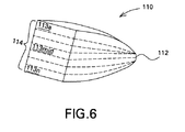
ここで図6を参照して述べると、互いの上に積層した複数の層113a〜113nを含む多層光学系110が示されており、これらの層は、入力面112と出力面114との間に延在して多角形の外形を有している。図示のように、多層光学系110の中間層が層113midである。層113mid以外の層の全てが、入力面112と出力面114との間に配置されているフォトン方向変更領域を含んでいる。但し、層113midがフォトン方向変更領域を含んでいてもよいし、113mid以外の他の層がフォトン方向変更領域を欠いていてもよいことを認められたい。図示の設計は、発散する電磁放射線が入力面112に入力されて、光学系多層によって方向変更され、出力面114から出力されて、例えば縮小円錐(コーン)型ファン・ビームのような縮小コーン・ビームとなることを可能にする。出力面114がフォトン方向変更領域に対して何処に位置しているかに依存して、ファン・ビームは、平行又は近平行となる場合もあるし、幾分か発散しているが入力電磁放射線に対しては依然集束したものとなる場合もある。加えて、個々の層の性質が共形であるため、多層光学系110を真空環境において用いることが可能になる。
Referring now to FIG. 6, a multi-layer
図7には、入力面212及び出力面214を含む多層光学系210が示されている。図6に示す実施形態の場合と同様に、多層光学系210は中間層を挟んで個々の層を含んでいる。図示の設計は、集束したファン・ビーム出力を可能にする。上で述べた各実施形態と同様に、個々の層の性質が共形であるため、多層光学系210を真空環境において用いることが可能になる。
FIG. 7 shows a multilayer
図8は、入力面312及び出力面314を有する多層光学系310を示す。各層は、個々の層のブランク又は型となる円錐150の上に配置されている。この設計を通じて、出力面314を出る出力ビームは曲面出力に成形され、この出力を単一曲面回折結晶(図示されていない)と結合して高単色性放射線のコーン・ビームの生成を可能にすることができる。例えばX線回折等の幾つかの異なる応用では単色性放射線が用いられる。高単色性放射線は、単結晶から回折することにより発生されるエネルギ範囲に近似的に等しい極めて狭いエネルギ範囲内の放射線である。曲面回折結晶は、例えば雲母、シリコン、ゲルマニウム又は白金のような任意の適当な物質で形成されることができ、結晶が、例えば円錐又は円筒の表面に沿うように曲面化されている。回折結晶として用いられる任意の物質の適合性は、物質の回折強度及び格子間隔に依存する。多層光学系310は、電磁放射線の線源と回折結晶との間に配置されて、回折後のビームにおいて最大フォトン束密度を得ることを認められたい。
FIG. 8 shows a multilayer
図5〜図7においてフィルタを光学系の入力面又は出力面に配置すると光学系の出力放射線が準単色性となる。準単色性放射線は、高単色性範囲よりも広いがX線源からの完全制動放射スペクトルよりも狭い限定された波長範囲内の放射線である。 5 to 7, when the filter is arranged on the input surface or output surface of the optical system, the output radiation of the optical system becomes quasi-monochromatic. Quasi-monochromatic radiation is radiation in a limited wavelength range that is wider than the high monochromatic range but narrower than the full bremsstrahlung spectrum from the x-ray source.
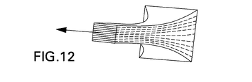
図9〜図12は、多層光学系のその他様々な可能性のある実施形態を示す。図9及び図10は、フォトン方向変更領域に出力面を有する多層光学系であって、これによりかかる光学系が大きく発散したビームを放出することを可能にする多層光学系を示す。図11及び図12は、出力面がそれぞれの入力面よりも小さい寸法となった多層光学系であって、大きく集束したビームを放出する多層光学系を示す。 9-12 illustrate various other possible embodiments of multilayer optics. 9 and 10 show a multilayer optical system having an output surface in the photon direction changing region, thereby enabling such an optical system to emit a highly divergent beam. 11 and 12 show a multilayer optical system in which an output surface is smaller than each input surface and emits a highly focused beam.
次に、図13を参照して、多層光学系を形成するのに用いられる装置について説明する。明確に述べると、多層光学系堆積アセンブリ400が、堆積室402及び可動式シャッタ装置410を含むものとして示されている。堆積室402は、例えば気相堆積又は熱噴射堆積等を含めた適当な堆積手法に用いられ得る。適当な気相堆積手法としては、スパッタリング、イオン埋め込み、イオンめっき、レーザ堆積、蒸着及びジェット気相堆積等が挙げられる。蒸着手法としては、熱、電子ビーム、又はかなりの物質の堆積を結果として生ずるその他任意の適当な手法がある。適当な熱噴射堆積としては、燃焼、電弧及びプラズマ噴射等がある。堆積室402は、堆積物質を堆積室402に導き入れる入力装置404を含んでいる。入力装置404は、各々が特定の堆積物質と関連する多数の入口ノズルを含み得ることを認められたい。ブランク420が堆積室402の内部に配置される。ブランク420は、図4及び図8に示す各実施形態に関して前述した芯50又は円錐150であってもよいし、堆積される層のための支持機構となる基材であってもよい。ブランク420は、所望のビーム・プロファイルと一致した実質的にあらゆる適当な幾何学的構成を取り得ることを認められたい。殆ど無限の数の適当な幾何学的構成の実例として幾つかを挙げると、円形ウェーハ、四角柱、円錐、円筒、及び卵形等がある。
Next, an apparatus used for forming a multilayer optical system will be described with reference to FIG. Specifically, a multi-layer
シャッタ装置410は、個々の層がフォトン方向変更領域を有するような多層光学系の形成を可能にする。明確に述べると、堆積物質が入力装置404を通じて堆積室402の内部に入力されると、シャッタ装置410がブランク420に対して方向Aに移動する。シャッタ装置410が方向Aに移動するにつれてシャッタ装置410の速度が低下すると、ブランク420に接触する堆積物質の量が次第に方向Aに増加し、これにより個々の層が異なる厚みを有すると共にフォトン方向変更領域を有するような多層光学系の形成が可能になる。シャッタ装置410の移動及び速度の制御は、マイクロコントローラ、マイクロプロセッサ又はコンピュータのようなディジタル式制御機構によって電子的に達成され得る。代替的には、移動の制御は手動で達成されてもよいし、空気式又は油圧式その他のように機械的に達成されてもよい。
The
各々の堆積物質が入力装置404を通じて堆積室402に入力されるにつれてシャッタ装置410を方向Aに沿って移動させることにより、個々の層をブランク420の上に堆積させることができ、図6に示す多層光学系のように共形の個々の層を有する多層光学系を形成することができる。多層光学系110のような多層光学系を形成する際に、堆積させるべき第一の層は中間層113midに隣接する層であってよい。次いで、層113aに至る後続の層を層113aを含めて堆積させることができる。次いで、部分的に形成されたこの多層光学系を裏返して、層113nに至る各層を層113nを含めて堆積させることができる。さらに、一定の速度で堆積物質を堆積室402に注入するとすると、シャッタ装置410が第一の速度で開始して、第二の異なる速度に移った後に第一の速度に戻るようにプログラムされている場合には、図7に示す多層光学系210のような多層光学系を形成することができる。尚、堆積室402での堆積物質の堆積速度を同様に変化させてもよいことを認められたい。
Individual layers can be deposited on the blank 420 by moving the
往復移動装置410を用いる代わりに、ブランク420に対して入力装置404を変化する速度で移動させることも可能である。さらに、入力装置404に対して堆積室402の内部のブランク420を変化する速度で移動させることも可能である。
Instead of using the
図14には、堆積室502及び可動式シャッタ410を含む多層光学系堆積アセンブリ500が図示されている。堆積室502は、蒸気流発生源である装置404と、1対の回転式スピンドル505とを含んでいる。スピンドル505は、方向Bに回転することが可能である。さらに、スピンドル505は各々、ブランク420と接触してブランク420を保持する尖端部を含んでいる。スピンドル505を同じ方向Bに回転させることにより、入力装置404を通じて堆積物質を堆積室502に導入しながらブランク420を回転させることができる。方向Aでのシャッタ装置410の移動及び方向Bでのブランク420の回転によって、図5に示す多層光学系10のような多層光学系の形成が可能になる。代替的には、スピンドル505は、第一の組の堆積ステップの間に非回転状態に留まって、図6の層113midに隣接する層を層113aまで形成することができる。次いで、スピンドル505を回転させて、部分的に形成された多層光学系を180度回転させて、第二の組の堆積ステップを行ない、層113nに至る各層を層113nを含めて形成して多層光学系110を形成することができる。
FIG. 14 illustrates a multilayer
シャッタ装置410を用いる代わりに、ブランク420をスピンドル505によって回転させながらブランク420に対して変化する速度で入力装置404を移動させることも可能である。さらに、入力装置404に対して変化する速度で堆積室402の内部のスピンドル505及びブランク420を移動させることも可能である。
Instead of using the
代替的には、ブランク420を回転させながら、入力装置404を静止したままにして、蒸気ビームをブランク420に沿って異なる高さに集束させてもよい。得られる異なる堆積速度は、光学系の上に深さ及び横方向に段階を付けた入力及び出力を形成し、図5に示す多層光学系10のような多層光学系の形成を可能にする。
Alternatively, the
図15は、本発明の一実施形態による多層光学系を形成する工程ステップを示す。ステップ600において、予め決められたフォトン透過係数と共に予め決められた屈折率を有する物質を堆積させる。物質は、芯、円錐又は多角形の支持機構であってよいブランク又は基材の上に堆積させられる。尚、ブランク又は基材は、芯50のように多層光学系の内部に組み入れられていてもよいし、円錐150のように単に型となっていてもよいことを認められたい。次いで、ステップ605において、一定のフォトン透過係数と共に所定の屈折率を有するもう一つの物質を、共形となり最小の空隙空間を有するような方法で前の物質の上に堆積させる。尚、各々の個々の層が1ナノメートル乃至数千ナノメートルの範囲の厚みで形成され得ることを認められたい。ステップ605の後に、ステップ600及びステップ605を相次いで繰り返して、例えば多数対の層を、各々の対が第一のフォトン透過係数と共に第一の屈折率を有する一つの層と第二のフォトン透過係数と共に第二の屈折率を有する第二の層とを有するようにして製造することができる。第一及び第二の物質の堆積は、例えば気相堆積、熱噴射堆積又は電気めっきのような任意の数の適当な工程によって達成され得る。前述のように、適当な気相堆積手法の実例としては、スパッタリング、イオン埋め込み、イオンめっき、レーザ堆積(堆積させたい物質(1又は複数)を気化させるためにレーザ・ビームを用いる)、蒸着、又はジェット気相堆積(堆積させたい物質(1又は複数)を気化させるために音波を用いる)等が挙げられる。また、前述のように、蒸着手法は、熱、電子ビーム、又はかなりの物質の堆積を結果として生ずるその他任意の適当な手法であってよい。適当な熱噴射堆積手法の実例としては、燃焼、電弧及びプラズマ噴射等がある。
FIG. 15 illustrates process steps for forming a multilayer optical system according to an embodiment of the invention. In
尚、堆積工程時に、部分的に形成された多層光学系を回転させたり、振動させたり、移動させたりしてよいことを認められたい。部分的に形成された多層光学系を回転させて、堆積物質を多層光学系の軸に沿って異なる速度で堆積させるための堆積工程を施すことができる。このようにして、光学系の入力において線源からさらに多量の電磁放射線を収集することを可能にする、多層光学系から平行又は近平行の電磁放射線ビームを出力することを可能にする、又は多層光学系から出力される電磁放射線ビームを一例としてペンシル・ビーム、コーン・ビーム、ファン・ビーム若しくは円弧状曲線として成形することを可能にするような様々な構成及びプロファイルの多層光学系を形成することができる。 It should be appreciated that the partially formed multilayer optical system may be rotated, vibrated, or moved during the deposition process. The partially formed multilayer optics can be rotated to provide a deposition process for depositing deposited material at different rates along the axis of the multilayer optics. In this way it is possible to collect a greater amount of electromagnetic radiation from the source at the input of the optical system, to output a parallel or near-parallel electromagnetic radiation beam from a multilayer optical system, or to multilayer Forming multi-layer optical systems with various configurations and profiles that allow the electromagnetic radiation beam output from the optical system to be shaped as a pencil beam, cone beam, fan beam or arcuate curve as an example Can do.
本発明の各実施形態による多層光学系は様々な工業的応用に利用され得る。例えば円形断面を有する準平行ビームを放出するように形成された多層光学系は、非破壊検査のようなX線回折応用及びX線後方散乱応用に利用され得る。円形断面を有する僅かに集束したビームを放出するように形成された多層光学系は、X線回折応用、蛍光X線法応用、医療診断又は侵襲型治療応用、及び非破壊検査応用に利用され得る。円形断面を有する大きく集束したビームを放出するように形成された多層光学系は、蛍光X線法応用、例えば微小腫瘍等の医療診断又は侵襲型治療応用、及び非破壊検査応用に利用され得る。円形断面を有する僅かに発散したビームを放出するように形成された多層光学系は、計算機式断層写真法応用及びX線診断システム応用に利用され得る。円形断面を有する大きく発散したビームを放出するように形成された多層光学系は、拡大視野を要求する非破壊検査応用、並びに大きい腫瘍の撮像及び治療のように拡大視野を要求する医療診断又は侵襲型撮像及び治療に利用され得る。 The multilayer optical system according to each embodiment of the present invention can be used in various industrial applications. For example, multilayer optics configured to emit a quasi-parallel beam with a circular cross-section can be used for X-ray diffraction applications such as non-destructive inspection and X-ray backscatter applications. Multi-layer optics configured to emit a slightly focused beam with a circular cross-section can be used for X-ray diffraction applications, X-ray fluorescence applications, medical diagnostic or invasive therapeutic applications, and non-destructive inspection applications . Multi-layer optics configured to emit a large focused beam with a circular cross-section can be used in fluorescent X-ray applications such as medical diagnostic or invasive therapeutic applications such as microtumors, and non-destructive testing applications. Multilayer optics configured to emit a slightly divergent beam having a circular cross-section can be utilized in computed tomography and x-ray diagnostic system applications. Multi-layer optics configured to emit a large divergent beam with a circular cross-section is suitable for non-destructive inspection applications that require an enlarged field of view, as well as medical diagnostics or invasiveness that require an enlarged field of view such as imaging and treatment of large tumors Can be used for mold imaging and therapy.
多様なビーム形状を放出するように形成された多層光学系の用途の一例は、腫瘍の治療のような医用侵襲型治療にあり、この場合には光学系の形状は腫瘍形状によって決定される。かかる多層光学系は、近傍の健全な組織を曝射せずに腫瘍にX線を集束させることを可能にし、周囲の健全な組織には最小の損傷しか与えずに標的治療を提供することができる。 One example of the use of multilayer optics configured to emit a variety of beam shapes is in medical invasive treatments such as tumor treatment, where the shape of the optics is determined by the tumor shape. Such multilayer optics can focus X-rays on the tumor without exposing nearby healthy tissue and provide targeted therapy with minimal damage to surrounding healthy tissue it can.
一つの平面内のファン・ビームであって、この平面の横断方向に準平行、僅かに集束した、大きく集束した、僅かに発散した又は大きく発散したファン・ビームを放出するように形成された多層光学系は、計算機式断層写真法応用、X線診断システム応用、及び非破壊検査応用に利用され得る。このファン・ビームは、線源と同じ又は線源よりも大きい発散を有し得る。代替的には、一つの平面内の準平行ファン・ビームであって、このファン平面の内部で準平行、僅かに集束した、大きく集束した、僅かに発散した又は大きく発散した準平行ファン・ビームを放出するように形成された多層光学系は、計算機式断層写真法応用、並びに非破壊検査応用及び医療検査応用に利用され得る矩形断面を有するビームを発生する。 Multilayer formed to emit a fan beam in one plane that is quasi-parallel, slightly focused, highly focused, slightly diverged, or highly divergent in the plane of the plane The optical system can be used in computed tomography applications, X-ray diagnostic system applications, and non-destructive inspection applications. The fan beam may have a divergence that is the same as or greater than the source. Alternatively, a quasi-parallel fan beam in one plane that is quasi-parallel, slightly focused, highly focused, slightly diverged or highly divergent within this fan plane Multi-layer optics configured to emit light generates a beam having a rectangular cross-section that can be utilized in computed tomography applications, as well as non-destructive and medical inspection applications.
また、一つの平面内のファン・ビームであって、ファン・ビーム平面の横断方向に僅かに又は大きく発散したファン・ビームを放出するように形成された多層光学系は、視野を拡大するための接写撮像のような医用侵襲型応用に利用され得る。ファン・ビーム平面の横断方向での発散は、線源発散に等しい又は線源発散よりも大きい。一つの平面内のファン・ビームであって、このファン平面に対して垂直に準平行、僅かに集束した、大きく集束した、僅かに発散した又は大きく発散したファン・ビームを放出するように形成された多層光学系は、計算機式断層写真法応用、X線診断システム応用及び非破壊検査応用に利用され得る。このファン・ビームは線源の発散と同じ又は線源の発散よりも大きい発散を有し得る。 Also, a multilayer optical system formed to emit a fan beam in one plane that diverges slightly or greatly in the transverse direction of the fan beam plane is provided for expanding the field of view. It can be used for medical invasive applications such as close-up imaging. The divergence in the transverse direction of the fan beam plane is equal to or greater than the source divergence. A fan beam in one plane, which is shaped to emit a fan beam that is quasi-parallel, slightly focused, highly focused, slightly focused, slightly diverged or highly divergent to the fan plane. The multilayer optical system can be used for computer tomography application, X-ray diagnostic system application and non-destructive inspection application. The fan beam may have a divergence that is the same as or greater than the divergence of the source.
回折結晶に結合された多層光学系は、強度が十分に大きい場合には医療撮像及び侵襲型治療に利用され得る準平行単色性ファン・ビームを発生し得る。かかる単色性撮像は、例えばコーン・ビーム・アーティファクトを抑えることにより分解能を高め、またビーム・ハードニング効果に伴い得るもののような縞/影を低減しつつ、患者側X線線量を低減する。 A multilayer optical system coupled to a diffractive crystal can generate a quasi-parallel monochromatic fan beam that can be used for medical imaging and invasive therapy if the intensity is sufficiently high. Such monochromatic imaging reduces patient-side x-ray dose while increasing resolution by, for example, suppressing cone beam artifacts and reducing fringes / shadows such as those that can accompany beam hardening effects.
図16は、例えば計算機式断層写真法(CT)スキャナのような対象検出システムに用いられる従来の取得システム700を示す。取得システム700は、支持構造から形成されたスキャナ702を含んでおり、スキャナ702は、1又は複数の静止型又は回転式分散型X線放射線線源(図16には示されていない)と、1又は複数の静止型又は回転式ディジタル検出器(図16には示されていない)とを内部に含んでいる。これらのことについては後にあらためて説明する。スキャナ702は、例えば手荷物若しくは鞄類、又は患者のような走査対象のためのテーブル704又は他の支持体を収容するように構成されている。テーブル704は、スキャナの中孔を通って移動して、撮像系列時に走査される撮像容積又は撮像平面に被検体を適当に配置することができる。
FIG. 16 shows a
システムはさらに、放射線源制御器706、テーブル制御器708及びデータ取得制御器710を含んでおり、全てシステム制御器712の指示の下に作用することができる。放射線源制御器706は、スキャナ702の周りの点から反対側の検出器素子に向かうX線放射線の放出のためのタイミングを調節する。このことについては後に説明する。放射線源制御器706は、分散型X線源の1又は複数の放出子に対し、測定データの多数の投影又はフレームを作成するための各々の時間的瞬間にトリガを印加することができる。幾つかの構成では、例えばX線放射線源制御器706は放射線の放出のためのトリガを逐次印加して、スキャナの周りでの測定データの隣接する又は隣接しないフレームを収集することができる。1回の検査系列において多くのかかるフレームを収集することができ、後述するように検出器素子に結合されたデータ取得制御器710は、検出器素子から信号を受け取り、記憶及び後の画像再構成のためにこれらの信号を処理する。1又は複数の線源が回転するような後述する構成では、線源制御器706はまた、分散型線源(1又は複数)が装着されているガントリの回転を命令することができる。ガントリの動作はまた、システム制御器712又は別個の制御器によって全体として制御され得る。次いで、テーブル制御器708はここでの状況では、テーブル及び被検体を放射線が放出される平面に適当に配置し、又は一般的には撮像される容積の内部に適当に配置する。テーブルは、用いられている撮像プロトコルに依存して撮像系列と撮像系列との間で変位してもよいし、幾つかの撮像系列の間に変位してもよい。また、1若しくは複数の検出器又は検出器弓形部分が回転するような後述する構成では、データ取得制御器710はまた、検出器(1又は複数)が装着されているガントリの回転を命令することができる。
The system further includes a
システム制御器712は一般的には、放射線源制御器706、テーブル制御器708及びデータ取得制御器710の動作を調節する。このように、システム制御器712は、放射線源制御器706がX線放射線の放出のためのトリガを印加すると共に、システム制御器によって定義される撮像系列時にかかる放出を協調させるようにすることができる。システム制御器はまた、特定の関心のある容積に対応する測定データを収集するような放出と協調して、又はヘリカル・モードのような様々な撮像モードで、テーブルの移動を調節することができる。また、システム制御器712は、線源(1若しくは複数)、検出器(1若しくは複数)又は両方が装着されているガントリの回転を協調させる。システム制御器712はまた、データ取得制御器710によって取得されたデータを受け取り、データの記憶及び処理を協調させる。
尚、本書に記載される各制御器及び多岐にわたるサーキットリは、ハードウェア・サーキットリ、ファームウェア又はソフトウェアによって定義され得ることを念頭に置かれたい。また、各制御器は図16に示すように別個のハードウェアであってもよいし、1個のハードウェアとして一体構成されていてもよい。例えば撮像系列の特定のプロトコルは一般的には、システム制御器によって実行されるコードによって定義される。また、スキャナによって取得される測定データに対して要求される初期的処理、調節、フィルタリング、及び他の動作は、図16に示す構成要素の1又は複数において実行され得る。例えば後述するように、検出器素子はデータ取得検出器の各ピクセルに対応する各位置に配置されたフォトダイオードの電荷の消耗を表わすアナログ信号を発生する。かかるアナログ信号はスキャナの内部の電子的構成要素によってディジタル信号へ変換されて、データ取得制御器710へ送信される。この点において部分的処理が生じてもよく、各信号は最終的にはシステム制御器に送信されて、さらなるフィルタリング及び処理を施すことができる。
It should be noted that each controller and various circuitry described herein may be defined by hardware circuitry, firmware or software. Each controller may be separate hardware as shown in FIG. 16, or may be integrally configured as one piece of hardware. For example, the specific protocol of the imaging sequence is generally defined by code executed by the system controller. Also, the initial processing, adjustment, filtering, and other operations required for the measurement data acquired by the scanner can be performed on one or more of the components shown in FIG. For example, as described below, the detector element generates an analog signal representing the charge depletion of a photodiode located at each location corresponding to each pixel of the data acquisition detector. Such analog signals are converted into digital signals by electronic components inside the scanner and transmitted to the
システム制御器712はまた、操作者インタフェイス714及び1又は複数のメモリ装置716に結合されている。操作者インタフェイスは、システム制御器と一体化されていてよく、一般的には、撮像系列を初期化したり、かかる系列を制御したり、撮像系列時に取得された測定データを操作したりするための操作者ワークステーションを含んでいる。メモリ装置716は、イメージング・システムに対してローカルに位置していてもよいし、システムから部分的に又は完全に遠隔に位置していてもよい。このように、撮像装置716は、ローカルの磁気式又は光学式メモリを含んでいてもよいし、再構成用の測定データのローカル又は遠隔の保管庫を含んでいてもよい。また、メモリ装置は、再構成用の未処理測定データ、部分的に処理された測定データ又は完全に処理された測定データを受け取るように構成されていてよい。モニタ(図示されていない)もまた操作者インタフェイス714に接続されており、走査データ、再構成データ、又は他の場合には処理済みデータの観察を可能にすることができる。
The
システム制御器712若しくは操作者インタフェイス714、又は任意の遠隔システム及びワークステーションは、画像処理及び再構成のためのソフトウェアを含んでいてよい。当業者には認められるように、かかるCT測定データ処理は、多くの数学的なアルゴリズム及び手法によって行なわれ得る。例えば従来のフィルタ補正逆投影手法を用いて、イメージング・システムによって取得されたデータを処理して再構成することができる。他の手法、及びフィルタ補正逆投影と共に用いられる手法を用いてもよい。遠隔インタフェイス718がシステムに含まれていてもよく、イメージング・システムからかかる遠隔処理ステーション又はメモリ装置にデータを送信することができる。
The
図17は、例えば図16のスキャナ702のような計算機式断層写真法(CT)スキャナのような対象検出システムに用いられている取得サブシステム800の部分を示す。明確に述べると、図17はX線管ヘッド840を示す。多層光学系10がシステム800の内部に組み入れられている。多層光学系10の連続した各層において高いX線吸収特性及び低いX線吸収特性をそれぞれ伴った交互に並んだ低屈折率物質及び高屈折率物質は、電磁放射線の全反射の原理を用いている。このため、ターゲット724から発する発散するX線ビームは入力面12に入り、方向変更されてフォトン・ビーム734となって出力面14を出る。所望の任意のビームを出力する多層光学系10を形成することができる。多層光学系10は、窓748の外部に配置されていても内部に配置されていてもよい。図17では、多層光学系10は、分かり易くするために両方の位置に示されている。
FIG. 17 illustrates a portion of an
多層光学系10は、図17に示すフォトン・ビーム734のように、応用に依存してエネルギが20keV以上の所望の形状のX線ビームを発生するような方法で形成され得る。図2〜図5に関して上述したように限定されたX線コーン・ビームを発生する多層光学系10を形成することができるが、出力面14が入力面12にさらに近付いて形成されており、すなわちフォトンが平行射線に方向変更される領域の前に配置されている点を例外とする。入力面12は平坦であってもよいし、ターゲット724からのX線の線源コーンの殆どを受け入れるように曲面化されていてもよい。これにより、入力X線ビームを所望の形状のビーム734に形成することができる。
The multilayer
ここではX線管及び検出器が撮像容積の周りを回転する第三世代CTイメージング・システムについて説明しているが、光学系は、第三世代技術の代替的な構成、例えばX線源及び検出器が固定された状態にあり、載置台がデータ取得時に対象を回転させるような産業用CT構成にも同等に応用可能である。 Although a third generation CT imaging system is described here in which the x-ray tube and detector rotate around the imaging volume, the optical system is an alternative configuration of third generation technology, such as an x-ray source and detection. The present invention is equally applicable to an industrial CT configuration in which the device is in a fixed state and the mounting table rotates the object at the time of data acquisition.
図18を詳細に参照して述べると、1対の光学装置10a、10bが示されている。これらの光学装置10a、10bの各々が図2〜図5に特に関して記載された光学装置10と同様のものである。光学装置10a、10bの相違は、一方が高X線エネルギを通過させるように形成され、他方が低X線エネルギを通過させるように形成されていることである。光学装置10a、10bによって線源スペクトルを成形する又はフィルタリングすると、サブビュー単位で鋭い高エネルギ遮断を伴うスペクトル形状を高速に発生する可能性を与え、これにより物質分離感度を高めて、殆どの位置合わせ問題を解消することができる。所望のスペクトル形状を有するスペクトルを高速の時間尺度で発生する能力は、かかる光学装置を多重エネルギ撮像に特に有用なものとする。
Referring to FIG. 18 in detail, a pair of
Kエッジ・フィルタを用いて、各々の光学系10a、10bに鋭い低エネルギ遮断を提供してもよい。一実施形態は、光学系10a、10bの両端に直接Kエッジ・フィルタを気相堆積させることを含んでいる。代替的には、Kエッジ・フィルタは、光学系10a、10bの出力又は入力と位置揃えされた別個の箔(フォイル)として形成されていてもよい。すると、各々の光学系10a、10bは、光学系に一体化されている又は光学系と別個の固有の異なるKエッジ・フィルタを有するものとなる。
Using K-edge filter may provide a sharp low energy cut off each of the
図示のように積層構成であってよい光学装置10a、10bは、取得サブシステム800(図17)のX線管ヘッド840のターゲット724と光学的に連絡している。明確に述べると、電子ビームをターゲット724の焦点スポット725に衝突させることにより形成されるX線733は焦点スポット725から光学装置10a、10bの入力面12に向かって伝播する。代替的には、焦点スポット725は各々、単一の連続したターゲット・スポット724に対して別々の個々のターゲット・スポットの内部に位置していてもよいし別個の非連続型ターゲットに位置していてもよい。次いで、X線733は、上述のように光学装置10a、10bによって集束されて、方向変更されたX線734として出力面を出る。この幾何学的構成は反復されて、かかるスポットの対のアレイを形成することができ、この場合には分散型X線源スポットのアレイが用いられるものとする。
A laminated structure which may optical device as illustrated 10 a, 10 b are in optical communication with the
高エネルギ信号と低エネルギ信号との分離を助けるために、多くの選択肢が可能である。一つのかかる構成は、別個のKエッジ・フィルタを設けた光学装置を用いて、エネルギ分布が互いに異なる二つの信号を発生する。このことを行なうために、一方の光学装置によって画像を撮影し、次いでこの光学装置及びKエッジ・フィルタの両方を用いて画像を再び撮影して低エネルギ・フォトンを除去する。これら二つの適当に正規化された信号を減算すると大部分が低エネルギである信号が得られ、一方、光学装置及びKエッジ・フィルタの組み合わせによって発生される信号は相対的に高エネルギ・フォトンを有する信号を発生する。 Many options are possible to help separate high and low energy signals. One such configuration uses an optical device with a separate K-edge filter to generate two signals with different energy distributions. To do this, an image is taken with one optical device, and then the image is taken again using both this optical device and a K-edge filter to remove low energy photons. Subtracting these two appropriately normalized signals results in a signal that is mostly low energy, while the signal generated by the combination of the optical device and the K-edge filter has a relatively high energy photon. A signal having
代替的には、二つの光学装置を少なくとも一つのKエッジ・フィルタと共に用いてもよい。二つの光学装置はX線方向変更を生ずると共に、重なり合っていてもいなくてもよい二つのフォトン・エネルギ範囲の透過を生ずる物質で製造される。これら二つの光学装置によって画像を撮影し、光学装置及び低エネルギを透過させる光学装置からのエネルギを遮断するKエッジ・フィルタを繰り返して、これら2枚の適当に正規化された画像を減算すると、低エネルギを透過させる光学系によって通過させられた低エネルギのみから導かれる画像を生ずる。この低エネルギ・スペクトル画像は、二つの光学装置及びKエッジ・フィルタの組み合わせからのフォトンによって形成された画像からこの適当に正規化された高エネルギ・スペクトル画像を減算することにより得ることができる。低エネルギ画像においてさらに鋭い低エネルギ遮断を得るためには、光学系から最も低いエネルギのフォトンを遮断する第二のKエッジ・フィルタを含めればよい。 Alternatively, two optical devices may be used with at least one K-edge filter. The two optical devices are made of materials that cause X-ray redirection and transmission of two photon energy ranges that may or may not overlap. Taking an image with these two optical devices, repeating the K-edge filter that cuts off the energy from the optical device and the low energy transmitting optical device, and subtracting these two appropriately normalized images, An image derived from only low energy passed by an optical system that transmits low energy is produced. This low energy spectral image can be obtained by subtracting this appropriately normalized high energy spectral image from the image formed by photons from the combination of the two optical devices and the K-edge filter. To obtain a sharper low energy block in low energy images, a second K-edge filter that blocks the lowest energy photons from the optical system may be included.
信号の間にさらに大きいエネルギ分離を提供し得るもう一つの選択肢は、光学装置を結合して異なる加速電位においてターゲットを分離し、各々の加速電位/光学系の組み合わせによって放出されるX線によって逐次的画像を撮影するものである。 Another option that can provide greater energy separation between the signals is to couple the optical device to separate the targets at different acceleration potentials, and sequentially by the X-rays emitted by each acceleration potential / optical system combination. The target image is taken.
異なるエネルギ分布によって発生される画像集合を迅速に、また可能な最善の統計学的鮮明度で得るために、フィルタ・ホイール775(図19)を用いて信号の逐次的フィルタリングを行なうことができる。例えば、二重エネルギ・フォトン分布を生成するために、フィルタ・ホイール775が全てのフォトンに対して不透過性である部分780と全てのX線に対して透過性である窓782とを含むようにすることができる。これらの窓782は、分かり易くする目的のみでフィルタ・ホイール775の部分的な周りにのみ図示されている。代替的には、窓782は、二つの光学装置が撮像に用いられるときに高エネルギ・スペクトルから低エネルギX線を遮断するのに必要とされるもののような適当なフィルタリング物質によって覆われていてもよい。フィルタ・ホイール775を回転させることにより、部分780を光学装置10aと検出器との間に配置し、これにより光学系10aによって透過させられる全てのX線が検出器に到達するのを遮断することができる。同時に、窓782を他方の光学装置10bと検出器との間に配置して、光学系10bによって透過させられる全てのX線が検出器に達するのを許すことができる。次いで、フィルタ・ホイール775を回転させて、窓782が光学装置10aと検出器750との間に配置されるようにし、部分780を光学装置10bと検出器750との間に配置して、光学装置10aのみからのX線が検出器によって受光されるようにする。
In order to obtain image sets generated by different energy distributions quickly and with the best possible statistical definition, the filter wheel 775 (FIG. 19) can be used to perform sequential filtering of the signal. For example, to generate a dual energy photon distribution, the
光学装置10a、10bは各々が幾つかのX線エネルギ・レベルをフィルタ除去するように作製される。明確に述べると、各々の光学装置10a、10bは、主に全反射によって光学系において幾つかのエネルギ・レベルのX線を選択的に方向変更する適当な光学物質から作製される。光学装置を作製するのに用いられる各物質の屈折率が、高エネルギ遮断を決定して、放出されるスペクトルの高エネルギ側端点を確定する。 The optical devices 10a , 10b are each made to filter out several x-ray energy levels. Specifically, each optical device 10a , 10b is made from a suitable optical material that selectively redirects several energy levels of x-rays in the optical system, primarily by total internal reflection. The refractive index of each material used to make the optical device determines the high energy cutoff and establishes the high energy side endpoint of the emitted spectrum.
上で述べたように、各光学装置は、複数の層を成して堆積した交互に並んだ高低の屈折率物質を含んでおり、個々の層がナノメートル厚み範囲にある。光学装置10の入力面12における各々の層は、45度以上等のように大きい線源角度を捕捉するように異なる程度まで曲面化されて、X線を緊密にコリメートされたファン形ビームに方向変更することができる。上で述べたように、Kエッジ・フィルタのような何らかの種類の低エネルギX線フィルタを光学装置10a、10bの高エネルギ・フィルタと組み合わせると、異なるスペクトル形状を実効的に発生することができる。低エネルギ・フィルタは、独立型箔の形態を取っていてよく、従来の光学系後方放出位置に配置されていても線源焦点スポットと光学装置との間に配置されていてもよい。代替的には、これらの低エネルギ・フィルタは、各々の光学系の入力端部又は出力端部の何れかに気相堆積又は化学めっきされていてよい。もう一つの可能性は、高屈折率物質内のドープ剤として光学装置に内部的にフィルタを組み入れるものである。低エネルギを光学系の透過からフィルタリングするさらにもう一つの方法は、選択的に荒い界面を有する光学系を製造するものである。表面荒さは、最も低いエネルギを散乱させるが、高エネルギの反射には影響を及ぼさない。加えて、内部的なフィルタの方法は、光学装置において全反射の臨界角を決定する異なる物質を選択することを含んでおり、この臨界角は、光学装置によって透過させられる最も高いX線エネルギを決定する。これらの光学系−フィルタの代替構成によって発生されるエネルギ・スペクトルは、線源の固有の制動放射放出とはかなり異なるように成形されて、遥かに鋭い高エネルギ遮断及び低エネルギ遮断を提供することができる。
As noted above, each optical device includes alternating high and low refractive index materials deposited in multiple layers, with individual layers in the nanometer thickness range. Each layer at the
2枚の異なるエネルギ分布画像を作成するもう一つの構成を図20に示しており、この構成は、2種の異なる光学系の二つの二半部10′、10″を共に接ぎ合わせて単一の光学装置10cを形成することを含んでいる。この形式の単一の光学装置10cの作成は、二つのターゲット・スポット725の重心の間の距離を潜在的に短縮するため、さらに小さい固有ビーム・スポット寸法を用いることが可能になり、ターゲット放出をより効率的に利用し、ターゲットの負荷を軽減し、画像位置合わせを改善する。一つのビームから他のビームへの切換えは、フィルタ・ホイール775のようなフィルタ・ホイールによって行なわれ得る。
Another configuration for creating two different energy distribution images is shown in FIG. 20, which consists of two
光学装置10′、10″の相違は、一方が高X線エネルギ734′を透過させ、他方が低X線エネルギ734″を透過させることである。光学装置10′、10″及び適当に組み入れられた各々の光学スペクトルの低エネルギ・フィルタによって線源スペクトルを成形する又はフィルタリングすると、サブビュー単位で鋭い高エネルギ遮断及び低エネルギ遮断を伴うスペクトル形状を高速に発生する可能性を与え、物質分離感度を高めて、殆どの位置合わせ問題を解消することができる。所望のスペクトル形状を有するスペクトルを高速の時間尺度で発生する能力は、かかる光学装置を多重エネルギ撮像に特に有用なものとする。取得サブシステム800(図17)において、光学装置10cはX線管ヘッド840のターゲット724と光学的に連絡する。明確に述べると、ターゲット724の焦点スポット725に電子ビームを衝突させることにより形成されるX線733は、焦点スポット725から光学装置10cの二つの二半部10′、10″のそれぞれ入力面12′、12″に向かって伝播される。次いで、X線733は、上述のように二つの二半部10′、10″によって二つの光学装置10a、10b(図18)に関して集束され、方向変更された高エネルギX線及び低エネルギX線734′、734″として出力面を出る。
The difference between the
さらにもう一つの構成は、低エネルギ光学系領域及び高エネルギ光学系領域をさらに近付けた空間的一体化を含む。単一の光学装置が多数の異なる組の高低の屈折率物質を含むようにして製造されて、一つの光学系が同時に多重エネルギ分布を発生するのを可能にすることができる。加えて、二重エネルギ・ビームを発生する光学系では、例えば低エネルギ・ビームを発生するのに用いられる光学装置の部分は、ドープ剤として内部的に組み入れられた対応する低エネルギ・フィルタ(例えばKエッジ・フィルタ)を有し得る。次いで、フィルタ・ホイールを、開いた窓と高エネルギX線を透過させる光学層のためのKエッジ・フィルタとの交互領域を単純に含むものとする。上で述べたように、フィルタ・ホイールのKエッジ・フィルタを光学系と先ず並べて撮影し、次いでフィルタ・ホイールの開いた窓を光学系と並べて撮影して逐次的画像を取得し、次いで適当に正規化された画像を減算することにより、本質的に同等のスポット形状(光学系のナノメートル層構造にわたって平均化されている)を有する空間的に一致するスポットによる二重エネルギ画像を作成することができる。 Yet another configuration includes a spatial integration that brings the low energy optics region and the high energy optics region closer together. A single optical device can be manufactured to include a number of different sets of high and low refractive index materials to allow a single optical system to generate multiple energy distributions simultaneously. In addition, in an optical system that generates a dual energy beam, for example, the portion of the optical device used to generate the low energy beam has a corresponding low energy filter (e.g., incorporated internally as a dopant) K edge filter). The filter wheel should then simply include alternating regions of open windows and K-edge filters for optical layers that transmit high energy x-rays. As mentioned above, the K-edge filter of the filter wheel is first photographed side by side with the optical system, then the open window of the filter wheel is photographed side by side with the optical system to obtain sequential images, and then appropriately Creating a dual energy image with spatially matched spots having essentially equivalent spot shapes (averaged over the nanometer layer structure of the optical system) by subtracting the normalized images Can do.
前述のように、Kエッジ・フィルタをドープ剤として組み入れることができる。かかるドーピングを行なう方法の一例として、ニッケルのKエッジを用いて低エネルギ・フォトンを遮断し、高屈折率層を全て一つの物質LiHで製造することを考える。すると、LiH層は、水素化リチウム及びニッケルを同時に堆積させることによりNiによってドープされ、所望の低エネルギを遮断するのに必要とされる最小量のニッケルを光学系の全長にわたって含ませることができる。所要のニッケル濃度は、光学系の全長、X線透過層の厚み、及び所望の低エネルギ遮断の程度から算出され得る。ミリメートル長程度の光学系の場合には、ニッケル原子の数は水素化リチウム分子の数よりも3桁以上小さいものとなる可能性が高い。 As mentioned above, a K-edge filter can be incorporated as a dopant. As an example of a method for performing such doping, let us consider that low-energy photons are blocked using a nickel K-edge, and that a high-refractive index layer is made of a single material, LiH. The LiH layer is then doped with Ni by simultaneously depositing lithium hydride and nickel, and can contain the minimum amount of nickel required to shut off the desired low energy over the entire length of the optical system. . The required nickel concentration can be calculated from the total length of the optical system, the thickness of the X-ray transmission layer, and the desired degree of low energy cutoff. In the case of an optical system of about millimeter length, the number of nickel atoms is likely to be three orders of magnitude smaller than the number of lithium hydride molecules.
図18〜図20に関して記載される二重エネルギ・システムでは、画像再構成投影の位置合わせ問題が縮小される。1対の光学装置10a、10bをフィルタ・ホイール775のような高速作動型シャッタと共に構成することにより、各々の光学装置を相次いで露光させて、これにより所与の時刻に何れのスペクトルを放出するかを制御することができる。かかる構成は、交互型スペクトル形状をミリ秒未満の時間尺度で提供することができ、これにより二つのエネルギについての投影集合の間の位置合わせ差を軽減する。
In the dual energy system described with respect to FIGS. 18-20, the alignment problem of the image reconstruction projection is reduced. By configuring a pair of
もう一つの構成では、二つの光学装置を用いることができ、一方は一つのX線焦点スポットに集束されて、低エネルギ・スペクトルを発生する等の所望の態様でX線スペクトルを成形する。第二の光学系は第二のX線焦点スポットに集束されて、高エネルギ・スペクトルを発生するようにX線スペクトルを成形する。各々の光学装置が出力を方向変更して、同じ空間容積を探査する。光学装置に入射するX線エネルギの範囲は、何れかのX線焦点スポットの適当な格子形成によって、又は単一のビームを多数のX線焦点スポット位置に方向変更することにより、高速に変化させることができる。例えば低エネルギ・スペクトルによって走査対象を探査するためには、反対側のX線焦点スポットを格子形成する。二つのX線焦点スポット位置が同じ加速電位を用いている場合には、光学装置が所望に応じてスペクトルをフィルタリングするようにすることができる。代替的には、各X線焦点スポット位置が異なる加速電位及び同様の光学装置を用いて、スペクトル差を生じさせることができる。さらにもう一つの実施形態では、加速電位及び光学装置特性の両方を変化させて、X線ビームのスペクトル特性を成形することができる。さらに、ビーム・フィルタを光学系と共に用いて、所望に応じてスペクトルをさらに成形することができる。ここに提示されるこれらのアプローチの何れも、X線スポットの分散型アレイのために多重エネルギ能力を提供するための反復を含み得る。 In another configuration, two optical devices can be used, one being focused into one x-ray focal spot and shaping the x-ray spectrum in a desired manner, such as generating a low energy spectrum. The second optical system is focused on the second x-ray focal spot and shapes the x-ray spectrum to produce a high energy spectrum. Each optical device redirects its output to explore the same spatial volume. The range of X-ray energy incident on the optical device is changed rapidly by appropriate grating formation of any X-ray focal spot or by redirecting a single beam to multiple X-ray focal spot positions. be able to. For example, to probe a scan object with a low energy spectrum, the opposite X-ray focal spot is gridded. If the two X-ray focal spot positions use the same acceleration potential, the optical device can filter the spectrum as desired. Alternatively, each X-ray focal spot location can use different acceleration potentials and similar optical devices to produce spectral differences. In yet another embodiment, both the accelerating potential and the optical device characteristics can be varied to shape the spectral characteristics of the X-ray beam. In addition, a beam filter can be used with the optics to further shape the spectrum as desired. Any of these approaches presented here may include iterations to provide multiple energy capabilities for a distributed array of x-ray spots.
かかる多重エネルギ・システムは、計算機式断層写真法以外の応用にも用いられ得る。例えば、かかるシステムを、標準的なX線投影撮像ばかりでなくX線回折に用いることができる。準単色性X線を用いることにより、光学系が所要のエネルギ強度を保って、走査速度を高いままに保つことが可能になる。 Such multi-energy systems can be used for applications other than computed tomography. For example, such a system can be used for X-ray diffraction as well as standard X-ray projection imaging. By using quasi-monochromatic X-rays, the optical system can maintain the required energy intensity and keep the scanning speed high.
本発明を限定された数の実施形態にのみ関連して詳細に記載したが、本発明はかかる開示された実施形態に限定されないことが容易に理解されよう。寧ろ、本発明は、本書では記載されていないが発明の要旨及び範囲に沿った任意の数の変形、代替構成、置換構成又は均等構成を組み入れるように改変することができる。例えば図17〜図20に特に関して記載される本発明の各実施形態は光学装置10、10a、10b、10cを参照しているが、かかる記載は説明を分かり易くするためのみのものであって、本書に記載される多層光学装置の任意のものを適宜組み入れ得ることを認められたい。さらに、上では単一エネルギ手法及び二重エネルギ手法について議論しているが、本発明は2よりも多いエネルギによるアプローチも包含している。加えて、本発明の様々な実施形態について記載したが、発明の各観点は所載の実施形態の幾つかのみを含んでいてもよいことを理解されたい。従って、本発明は、以上の記載によって制限されるのではなく、特許請求の範囲によってのみ制限されるものとする。 Although the invention has been described in detail in connection with only a limited number of embodiments, it will be readily understood that the invention is not limited to such disclosed embodiments. Rather, the invention can be modified to incorporate any number of variations, alternatives, substitutions or equivalents not described herein, but within the spirit and scope of the invention. For example, the embodiments of the invention described with particular reference to Figures 17 to 20 refer to optical devices 10,10 a, 10 b, 10 c , such description is intended only for clarity of description It should be appreciated that any of the multilayer optical devices described herein may be incorporated as appropriate. In addition, although the single energy and dual energy approaches are discussed above, the present invention also encompasses approaches with more than two energies. In addition, while various embodiments of the invention have been described, it should be understood that each aspect of the invention may include only some of the described embodiments. Accordingly, the invention is not limited by the foregoing description, but is only limited by the scope of the appended claims.
10 多層光学系
10′、10″ 光学系の二半部
10a、10b、10c 光学装置
12、12′、12″ 入力面
14 出力面
15、19、23、27 低屈折率高X線吸収物質層
16、20、24 高屈折率物質高X線透過性物質層
17、21、25 フォトン方向変更領域
34 電磁放射線源
36 ビーム
38、40、42 発散する電磁放射線ビーム
44 準平行フォトン・ビーム
50 芯
110 多層光学系
112 入力面
113a〜113n 層
113mid 中間層
114 出力面
150 円錐
210、310 多層光学系
212、312 入力面
214、314 出力面
400、500 多層光学系堆積アセンブリ
402、502 堆積室
404 入力装置
410 可動式シャッタ装置
420 ブランク
505 スピンドル
700 取得システム
702 スキャナ
704 テーブル
706 放射線源制御器
708 テーブル制御器
710 データ取得制御器
712 システム制御器
714 操作者インタフェイス
716 メモリ装置
718 遠隔インタフェイス
724 ターゲット
725 焦点スポット
726
733 X線
734 フォトン・ビーム
734′ 高X線エネルギ
734″ 低X線エネルギ
742
744
748 窓
775 フィルタ・ホイール
780 不透過性部分
782 透過性窓
800 取得サブシステム
840 X線管ヘッド
10
733
744
748
Claims (10)
を備えた、請求項1に記載のアセンブリ。 Some of the energy from the beam having transmitted through a filtering mechanism for filtering out by the optical device, fill are integrated into filter device and the optical device is provided external to said optical device and a filtering mechanism is at least one of a data device, assembly according to claim 1.
前記第一のX線エネルギーよりも低い第二のX線エネルギを透過させる第二の光学的部分と
を備え、
前記第一及び第二の光学的部分の何れか又は両方が少なくとも3層の共形固相層を含んでおり、該固相層同士の間の界面が無間隙であり、前記少なくとも3層の共形固相層は内部全反射を行う少なくとも一つのX線方向変更領域を含んでおり、前記少なくとも3層の内の少なくとも2層が異なる屈折率を有している、
光学装置のアレイ。 A first optical portion that transmits first X-ray energy through total internal reflection ;
A second optical portion that transmits a second X-ray energy that is lower than the first X-ray energy ;
Either or both of the first and second optical portions include at least three conformal solid phase layers, the interface between the solid phase layers is non-gap, and the at least three layers The conformal solid phase layer includes at least one X-ray direction changing region that performs total internal reflection, and at least two of the at least three layers have different refractive indexes .
An array of optical devices.
前記第一の光学的部分は高X線エネルギを通過させる物質で形成されており、前記第二の光学的部分は低X線エネルギを通過させる物質で形成されている、請求項7に記載のアレイ。 The first and second optical portions include opposing halves forming a single optical device;
8. The first optical portion is formed of a material that transmits high X-ray energy, and the second optical portion is formed of a material that transmits low X-ray energy. array.
フィルタリング機構を用いて前記光学装置により透過させられたより低いX線エネルギで第二の画像を収集するステップであって、前記フィルタリング機構は、前記光学装置に対して外部に設けられているフィルタリング装置及び前記光学装置に一体化されているフィルタリング装置の少なくとも一方である、前記ステップと、
前記第一の画像から前記第二の画像を減算するステップと、
を備えた方法。 A step to gather the first image in X-ray energy through the optical device using the total internal reflection,
Collecting a second image with lower X-ray energy transmitted by the optical device using a filtering mechanism, wherein the filtering mechanism is provided external to the optical device and at least one of a filtering device which is integrated with the optical device, and the step,
Subtracting the second image from the first image;
With a method.
該電子発生源からの電子により衝突されると発散するX線を形成するターゲットと、
該ターゲットを収容した真空室と、
前記X線が該真空室から出るときに通る窓と、
発散する前記X線を受け、所望の範囲のX線エネルギを透過させるように構成されている請求項1乃至5のいずれかに記載の光学アセンブリと
を備える、
多重エネルギ・イメージング・システム。
An electron source;
A target that forms X-rays that diverge when impacted by electrons from the electron source;
A vacuum chamber containing the target;
A window through which the X-ray exits the vacuum chamber;
Receiving said X-rays diverging, Ru and an optical assembly according to any of claims 1 to 5 is configured to transmit the X-ray energy in the desired range,
Multi-energy imaging system.
Applications Claiming Priority (3)
| Application Number | Priority Date | Filing Date | Title |
|---|---|---|---|
| US11/952,498 | 2007-12-07 | ||
| US11/952,498 US7742566B2 (en) | 2007-12-07 | 2007-12-07 | Multi-energy imaging system and method using optic devices |
| PCT/US2008/085312 WO2009076111A2 (en) | 2007-12-07 | 2008-12-03 | A multi-energy imaging system and method using optic devices |
Publications (3)
| Publication Number | Publication Date |
|---|---|
| JP2011506929A JP2011506929A (en) | 2011-03-03 |
| JP2011506929A5 JP2011506929A5 (en) | 2013-01-31 |
| JP5476315B2 true JP5476315B2 (en) | 2014-04-23 |
Family
ID=40512437
Family Applications (1)
| Application Number | Title | Priority Date | Filing Date |
|---|---|---|---|
| JP2010537025A Expired - Fee Related JP5476315B2 (en) | 2007-12-07 | 2008-12-03 | Optical assembly, array of optical devices, multi-energy imaging system and method |
Country Status (4)
| Country | Link |
|---|---|
| US (1) | US7742566B2 (en) |
| EP (1) | EP2229682B1 (en) |
| JP (1) | JP5476315B2 (en) |
| WO (1) | WO2009076111A2 (en) |
Families Citing this family (30)
| Publication number | Priority date | Publication date | Assignee | Title |
|---|---|---|---|---|
| US20100185319A1 (en) * | 2004-01-12 | 2010-07-22 | Titech Gmbh | Device and Method for Separating Bulk Material |
| US9333577B2 (en) | 2008-08-29 | 2016-05-10 | General Electric Company | Electro discharge machining apparatus and method |
| WO2010051469A1 (en) * | 2008-10-30 | 2010-05-06 | Kenneth Oosting | X-ray beam processor |
| US8369674B2 (en) | 2009-05-20 | 2013-02-05 | General Electric Company | Optimizing total internal reflection multilayer optics through material selection |
| US8208602B2 (en) * | 2010-02-22 | 2012-06-26 | General Electric Company | High flux photon beams using optic devices |
| US8483354B1 (en) * | 2010-02-26 | 2013-07-09 | Orbital Therapy Llc | Reducing imaging artifacts |
| KR101430121B1 (en) * | 2010-04-06 | 2014-08-14 | 삼성전자주식회사 | Apparatus of Processing Images in Multi-Energy X-ray System and Method for Processing the Images |
| US8311184B2 (en) | 2010-08-30 | 2012-11-13 | General Electric Company | Fan-shaped X-ray beam imaging systems employing graded multilayer optic devices |
| FR2967887B1 (en) * | 2010-11-26 | 2018-01-19 | General Electric Company | COMPACT MAMMOGRAPH, AND ASSOCIATED MAMMOGRAPHING METHOD |
| US8744048B2 (en) | 2010-12-28 | 2014-06-03 | General Electric Company | Integrated X-ray source having a multilayer total internal reflection optic device |
| CN102157216B (en) * | 2011-02-17 | 2012-11-21 | 浙江工业大学 | Manufacturing method of combined SU-8-material inlaid two-dimensional focusing X-ray refraction lens |
| CN102157217B (en) * | 2011-03-16 | 2013-01-16 | 浙江工业大学 | Parabolic two-dimensional focusing X-ray compound refractive lens |
| US8761346B2 (en) | 2011-07-29 | 2014-06-24 | General Electric Company | Multilayer total internal reflection optic devices and methods of making and using the same |
| EP2740127B1 (en) * | 2011-08-06 | 2017-11-29 | Rigaku Innovative Technologies, Inc. | Nanotube based device for guiding x-ray photons and neutrons |
| US8693631B2 (en) | 2011-08-29 | 2014-04-08 | General Electric Company | Craser device, imaging system and method |
| US20130142312A1 (en) * | 2011-12-02 | 2013-06-06 | Canon Kabushiki Kaisha | X-ray waveguide and x-ray waveguide system |
| CN103137233A (en) * | 2011-12-02 | 2013-06-05 | 佳能株式会社 | X-ray waveguide and X-ray waveguide system |
| JP6016386B2 (en) | 2012-03-09 | 2016-10-26 | キヤノン株式会社 | X-ray optical device |
| JP6108671B2 (en) | 2012-03-13 | 2017-04-05 | キヤノン株式会社 | Radiography equipment |
| JP6016391B2 (en) | 2012-03-14 | 2016-10-26 | キヤノン株式会社 | X-ray optical apparatus and adjustment method thereof |
| CN103886928B (en) * | 2014-04-15 | 2017-01-11 | 西安石油大学 | Transmission-type Fibonacci thin film lens for soft X-ray wave band and designing and manufacturing method of lens |
| NZ727182A (en) * | 2014-05-08 | 2018-05-25 | L Livermore Nat Security Llc | Methods for 2-color radiography with laser-compton x-ray sources |
| JP6397690B2 (en) * | 2014-08-11 | 2018-09-26 | 株式会社日立ハイテクノロジーズ | X-ray transmission inspection apparatus and foreign object detection method |
| EP3322341B1 (en) * | 2015-07-14 | 2019-03-27 | Koninklijke Philips N.V. | Imaging with modulated x-ray radiation |
| JP6533006B2 (en) * | 2015-07-14 | 2019-06-19 | コーニンクレッカ フィリップス エヌ ヴェKoninklijke Philips N.V. | Imaging with enhanced x-ray radiation |
| US10677744B1 (en) * | 2016-06-03 | 2020-06-09 | U.S. Department Of Energy | Multi-cone x-ray imaging Bragg crystal spectrometer |
| CN108983334A (en) * | 2018-09-05 | 2018-12-11 | 中国科学院上海应用物理研究所 | A kind of photon shutter device |
| US11287585B2 (en) | 2020-03-11 | 2022-03-29 | Nubis Communications, Inc. | Optical fiber-to-chip interconnection |
| US11071506B1 (en) * | 2020-04-28 | 2021-07-27 | Wisconsin Alumni Research Foundation | X-ray imaging device providing enhanced spatial resolution by energy encoding |
| EP4305477A1 (en) * | 2021-03-11 | 2024-01-17 | Nubis Communications, Inc. | Optical fiber-to-chip interconnection |
Family Cites Families (31)
| Publication number | Priority date | Publication date | Assignee | Title |
|---|---|---|---|---|
| JPS6189547A (en) * | 1984-10-08 | 1986-05-07 | Rigaku Denki Kogyo Kk | X-ray spectroscopic element |
| US4684565A (en) | 1984-11-20 | 1987-08-04 | Exxon Research And Engineering Company | X-ray mirrors made from multi-layered material |
| JPH02210299A (en) * | 1989-02-10 | 1990-08-21 | Olympus Optical Co Ltd | Optical system for x ray and multi-layered film reflecting mirror used for the same |
| JP2883122B2 (en) * | 1989-10-20 | 1999-04-19 | オリンパス光学工業株式会社 | X-ray microscope |
| FR2665261A1 (en) * | 1990-07-24 | 1992-01-31 | Philips Electronique Lab | X - RAY DIFFRACTOMETRY DEVICE AND USE THEREOF. |
| US5497008A (en) * | 1990-10-31 | 1996-03-05 | X-Ray Optical Systems, Inc. | Use of a Kumakhov lens in analytic instruments |
| US5192869A (en) * | 1990-10-31 | 1993-03-09 | X-Ray Optical Systems, Inc. | Device for controlling beams of particles, X-ray and gamma quanta |
| US5175755A (en) * | 1990-10-31 | 1992-12-29 | X-Ray Optical System, Inc. | Use of a kumakhov lens for x-ray lithography |
| US5216699A (en) * | 1991-09-17 | 1993-06-01 | Olympus Optical Co., Ltd. | X-ray microscope |
| US6271534B1 (en) * | 1994-07-08 | 2001-08-07 | Muradin Abubekirovich Kumakhov | Device for producing the image of an object using a flux of neutral or charged particles, and an integrated lens for converting such flux of neutral or charged particles |
| US5570408A (en) * | 1995-02-28 | 1996-10-29 | X-Ray Optical Systems, Inc. | High intensity, small diameter x-ray beam, capillary optic system |
| US5604353A (en) | 1995-06-12 | 1997-02-18 | X-Ray Optical Systems, Inc. | Multiple-channel, total-reflection optic with controllable divergence |
| US5745547A (en) * | 1995-08-04 | 1998-04-28 | X-Ray Optical Systems, Inc. | Multiple channel optic |
| CN1069136C (en) * | 1996-02-17 | 2001-08-01 | 北京师范大学 | Integral X-ray lens and manufacturing method thereof and equipment using the same |
| JPH11352297A (en) * | 1998-06-11 | 1999-12-24 | Rigaku Denki Kk | X-ray spectral element |
| GB9815968D0 (en) * | 1998-07-23 | 1998-09-23 | Bede Scient Instr Ltd | X-ray focusing apparatus |
| US6389100B1 (en) * | 1999-04-09 | 2002-05-14 | Osmic, Inc. | X-ray lens system |
| US6278764B1 (en) * | 1999-07-22 | 2001-08-21 | The Regents Of The Unviersity Of California | High efficiency replicated x-ray optics and fabrication method |
| RU2164361C1 (en) * | 1999-10-18 | 2001-03-20 | Кумахов Мурадин Абубекирович | Lens for controlling radiation in the form of neutral or charged particles; method for manufacturing these lenses; analytical apparatus, beam therapy apparatus, contact and projection lithography devices using these lenses |
| US6317483B1 (en) * | 1999-11-29 | 2001-11-13 | X-Ray Optical Systems, Inc. | Doubly curved optical device with graded atomic planes |
| RU2187160C1 (en) * | 2000-12-29 | 2002-08-10 | Кумахов Мурадин Абубекирович | X-ray lithographer |
| DE60213994T2 (en) | 2001-06-19 | 2006-12-07 | X-Ray Optical Systems, Inc., East Greenbush | WAVE LENGTH-DISPERSIVE X-RAY FLUORESCENT SYSTEM WITH FOCUSING SOUND OPTICS AND A FOCUSING MONOCHROMATOR FOR COLLAPSE |
| JP2003149392A (en) * | 2001-11-09 | 2003-05-21 | Tohken Co Ltd | X-ray intensifying reflecting plate and x-ray inspection device |
| AU2002364525A1 (en) * | 2001-12-04 | 2003-06-17 | X-Ray Optical Systems, Inc. | X-ray fluorescence analyser for analysing fluid streams using a semiconductor-type detector and focusing means |
| US6782073B2 (en) * | 2002-05-01 | 2004-08-24 | Siemens Medical Solutions Usa, Inc. | Planning system for convergent radiation treatment |
| US7120222B2 (en) * | 2003-06-05 | 2006-10-10 | General Electric Company | CT imaging system with multiple peak x-ray source |
| US7440546B2 (en) * | 2006-12-06 | 2008-10-21 | Uchicago Argonne, Llc | Method of making and structure of multilayer laue lens for focusing hard x-rays |
| US7412131B2 (en) | 2007-01-02 | 2008-08-12 | General Electric Company | Multilayer optic device and system and method for making same |
| US7366374B1 (en) | 2007-05-22 | 2008-04-29 | General Electric Company | Multilayer optic device and an imaging system and method using same |
| US20090041198A1 (en) | 2007-08-07 | 2009-02-12 | General Electric Company | Highly collimated and temporally variable x-ray beams |
| US7508911B1 (en) | 2007-09-19 | 2009-03-24 | General Electric Company | X-ray imaging system and methods of using and forming an array of optic devices therein |
-
2007
- 2007-12-07 US US11/952,498 patent/US7742566B2/en not_active Expired - Fee Related
-
2008
- 2008-12-03 EP EP08859503.8A patent/EP2229682B1/en not_active Not-in-force
- 2008-12-03 WO PCT/US2008/085312 patent/WO2009076111A2/en active Application Filing
- 2008-12-03 JP JP2010537025A patent/JP5476315B2/en not_active Expired - Fee Related
Also Published As
| Publication number | Publication date |
|---|---|
| US7742566B2 (en) | 2010-06-22 |
| US20090147922A1 (en) | 2009-06-11 |
| EP2229682A2 (en) | 2010-09-22 |
| WO2009076111A2 (en) | 2009-06-18 |
| JP2011506929A (en) | 2011-03-03 |
| EP2229682B1 (en) | 2013-08-14 |
| WO2009076111A3 (en) | 2009-08-20 |
Similar Documents
| Publication | Publication Date | Title |
|---|---|---|
| JP5476315B2 (en) | Optical assembly, array of optical devices, multi-energy imaging system and method | |
| JP6050455B2 (en) | Fan-shaped X-ray beam imaging system using a multilayered optical device with gradients | |
| US8208602B2 (en) | High flux photon beams using optic devices | |
| US7508911B1 (en) | X-ray imaging system and methods of using and forming an array of optic devices therein | |
| US10416099B2 (en) | Method of performing X-ray spectroscopy and X-ray absorption spectrometer system | |
| JP7171190B2 (en) | Source-detector device | |
| JP5138946B2 (en) | Focus-detector device for X-ray equipment | |
| US7366374B1 (en) | Multilayer optic device and an imaging system and method using same | |
| US7412131B2 (en) | Multilayer optic device and system and method for making same | |
| JP3090471B2 (en) | Particle, X-ray and gamma-ray quantum beam controller | |
| JPS63501735A (en) | Improved X-ray attenuation method and device | |
| US11085888B2 (en) | X-ray CT microscopy system and method utilizing lattice sampling | |
| US20080075230A1 (en) | Compact e-beam source for generating X-rays | |
| US20070030947A1 (en) | X-ray device with improved efficiency | |
| JP7023897B2 (en) | X-ray device and its operation method | |
| EP3602020A1 (en) | Method of performing x-ray spectroscopy and x-ray absorption spectrometer system | |
| US10925556B2 (en) | Imaging with modulated X-ray radiation | |
| Troussel et al. | Development of supermirrors for high-resolution x-ray LMJ microscopes |
Legal Events
| Date | Code | Title | Description |
|---|---|---|---|
| A521 | Request for written amendment filed |
Free format text: JAPANESE INTERMEDIATE CODE: A523 Effective date: 20111201 |
|
| A621 | Written request for application examination |
Free format text: JAPANESE INTERMEDIATE CODE: A621 Effective date: 20111201 |
|
| A521 | Request for written amendment filed |
Free format text: JAPANESE INTERMEDIATE CODE: A523 Effective date: 20121203 |
|
| A977 | Report on retrieval |
Free format text: JAPANESE INTERMEDIATE CODE: A971007 Effective date: 20130913 |
|
| A131 | Notification of reasons for refusal |
Free format text: JAPANESE INTERMEDIATE CODE: A131 Effective date: 20130924 |
|
| A521 | Request for written amendment filed |
Free format text: JAPANESE INTERMEDIATE CODE: A523 Effective date: 20131106 |
|
| TRDD | Decision of grant or rejection written | ||
| A01 | Written decision to grant a patent or to grant a registration (utility model) |
Free format text: JAPANESE INTERMEDIATE CODE: A01 Effective date: 20140114 |
|
| A61 | First payment of annual fees (during grant procedure) |
Free format text: JAPANESE INTERMEDIATE CODE: A61 Effective date: 20140207 |
|
| R150 | Certificate of patent or registration of utility model |
Ref document number: 5476315 Country of ref document: JP Free format text: JAPANESE INTERMEDIATE CODE: R150 Free format text: JAPANESE INTERMEDIATE CODE: R150 |
|
| R250 | Receipt of annual fees |
Free format text: JAPANESE INTERMEDIATE CODE: R250 |
|
| R250 | Receipt of annual fees |
Free format text: JAPANESE INTERMEDIATE CODE: R250 |
|
| R250 | Receipt of annual fees |
Free format text: JAPANESE INTERMEDIATE CODE: R250 |
|
| R250 | Receipt of annual fees |
Free format text: JAPANESE INTERMEDIATE CODE: R250 |
|
| LAPS | Cancellation because of no payment of annual fees |