JP5466694B2 - 発光デバイス・ディスプレイのためのシステムおよび駆動方法 - Google Patents
発光デバイス・ディスプレイのためのシステムおよび駆動方法 Download PDFInfo
- Publication number
- JP5466694B2 JP5466694B2 JP2011504297A JP2011504297A JP5466694B2 JP 5466694 B2 JP5466694 B2 JP 5466694B2 JP 2011504297 A JP2011504297 A JP 2011504297A JP 2011504297 A JP2011504297 A JP 2011504297A JP 5466694 B2 JP5466694 B2 JP 5466694B2
- Authority
- JP
- Japan
- Prior art keywords
- pixel circuit
- transistor
- terminal
- programming
- current
- Prior art date
- Legal status (The legal status is an assumption and is not a legal conclusion. Google has not performed a legal analysis and makes no representation as to the accuracy of the status listed.)
- Active
Links
- 238000000034 method Methods 0.000 title description 43
- 239000003990 capacitor Substances 0.000 claims description 56
- 239000011159 matrix material Substances 0.000 claims description 6
- 230000036962 time dependent Effects 0.000 claims description 3
- 239000010409 thin film Substances 0.000 claims description 2
- 238000005516 engineering process Methods 0.000 description 31
- 238000010586 diagram Methods 0.000 description 26
- 229920001621 AMOLED Polymers 0.000 description 22
- 101100191136 Arabidopsis thaliana PCMP-A2 gene Proteins 0.000 description 13
- 101100048260 Saccharomyces cerevisiae (strain ATCC 204508 / S288c) UBX2 gene Proteins 0.000 description 13
- 229910021417 amorphous silicon Inorganic materials 0.000 description 13
- 101100422768 Saccharomyces cerevisiae (strain ATCC 204508 / S288c) SUL2 gene Proteins 0.000 description 12
- 229910021420 polycrystalline silicon Inorganic materials 0.000 description 11
- 229920005591 polysilicon Polymers 0.000 description 11
- 239000004065 semiconductor Substances 0.000 description 10
- 230000000694 effects Effects 0.000 description 8
- 229910021424 microcrystalline silicon Inorganic materials 0.000 description 8
- 229910021423 nanocrystalline silicon Inorganic materials 0.000 description 8
- 230000008569 process Effects 0.000 description 8
- 230000000295 complement effect Effects 0.000 description 6
- 241001270131 Agaricus moelleri Species 0.000 description 4
- 238000004519 manufacturing process Methods 0.000 description 4
- 230000007246 mechanism Effects 0.000 description 4
- 230000002123 temporal effect Effects 0.000 description 4
- XUIMIQQOPSSXEZ-UHFFFAOYSA-N Silicon Chemical compound [Si] XUIMIQQOPSSXEZ-UHFFFAOYSA-N 0.000 description 2
- 238000003491 array Methods 0.000 description 2
- 239000002184 metal Substances 0.000 description 2
- 230000003071 parasitic effect Effects 0.000 description 2
- 230000002093 peripheral effect Effects 0.000 description 2
- 101150018075 sel-2 gene Proteins 0.000 description 2
- 229910052710 silicon Inorganic materials 0.000 description 2
- 239000010703 silicon Substances 0.000 description 2
- 238000004088 simulation Methods 0.000 description 2
- 230000008901 benefit Effects 0.000 description 1
- 230000015556 catabolic process Effects 0.000 description 1
- 230000008859 change Effects 0.000 description 1
- 238000006731 degradation reaction Methods 0.000 description 1
- 230000010354 integration Effects 0.000 description 1
- 239000004973 liquid crystal related substance Substances 0.000 description 1
- 230000007774 longterm Effects 0.000 description 1
- 238000012986 modification Methods 0.000 description 1
- 230000004048 modification Effects 0.000 description 1
- 239000000758 substrate Substances 0.000 description 1
Images


Classifications
-
- H—ELECTRICITY
- H05—ELECTRIC TECHNIQUES NOT OTHERWISE PROVIDED FOR
- H05B—ELECTRIC HEATING; ELECTRIC LIGHT SOURCES NOT OTHERWISE PROVIDED FOR; CIRCUIT ARRANGEMENTS FOR ELECTRIC LIGHT SOURCES, IN GENERAL
- H05B45/00—Circuit arrangements for operating light-emitting diodes [LED]
- H05B45/60—Circuit arrangements for operating LEDs comprising organic material, e.g. for operating organic light-emitting diodes [OLED] or polymer light-emitting diodes [PLED]
-
- G—PHYSICS
- G09—EDUCATION; CRYPTOGRAPHY; DISPLAY; ADVERTISING; SEALS
- G09G—ARRANGEMENTS OR CIRCUITS FOR CONTROL OF INDICATING DEVICES USING STATIC MEANS TO PRESENT VARIABLE INFORMATION
- G09G3/00—Control arrangements or circuits, of interest only in connection with visual indicators other than cathode-ray tubes
- G09G3/20—Control arrangements or circuits, of interest only in connection with visual indicators other than cathode-ray tubes for presentation of an assembly of a number of characters, e.g. a page, by composing the assembly by combination of individual elements arranged in a matrix no fixed position being assigned to or needed to be assigned to the individual characters or partial characters
- G09G3/22—Control arrangements or circuits, of interest only in connection with visual indicators other than cathode-ray tubes for presentation of an assembly of a number of characters, e.g. a page, by composing the assembly by combination of individual elements arranged in a matrix no fixed position being assigned to or needed to be assigned to the individual characters or partial characters using controlled light sources
- G09G3/30—Control arrangements or circuits, of interest only in connection with visual indicators other than cathode-ray tubes for presentation of an assembly of a number of characters, e.g. a page, by composing the assembly by combination of individual elements arranged in a matrix no fixed position being assigned to or needed to be assigned to the individual characters or partial characters using controlled light sources using electroluminescent panels
- G09G3/32—Control arrangements or circuits, of interest only in connection with visual indicators other than cathode-ray tubes for presentation of an assembly of a number of characters, e.g. a page, by composing the assembly by combination of individual elements arranged in a matrix no fixed position being assigned to or needed to be assigned to the individual characters or partial characters using controlled light sources using electroluminescent panels semiconductive, e.g. using light-emitting diodes [LED]
- G09G3/3208—Control arrangements or circuits, of interest only in connection with visual indicators other than cathode-ray tubes for presentation of an assembly of a number of characters, e.g. a page, by composing the assembly by combination of individual elements arranged in a matrix no fixed position being assigned to or needed to be assigned to the individual characters or partial characters using controlled light sources using electroluminescent panels semiconductive, e.g. using light-emitting diodes [LED] organic, e.g. using organic light-emitting diodes [OLED]
- G09G3/3225—Control arrangements or circuits, of interest only in connection with visual indicators other than cathode-ray tubes for presentation of an assembly of a number of characters, e.g. a page, by composing the assembly by combination of individual elements arranged in a matrix no fixed position being assigned to or needed to be assigned to the individual characters or partial characters using controlled light sources using electroluminescent panels semiconductive, e.g. using light-emitting diodes [LED] organic, e.g. using organic light-emitting diodes [OLED] using an active matrix
- G09G3/3233—Control arrangements or circuits, of interest only in connection with visual indicators other than cathode-ray tubes for presentation of an assembly of a number of characters, e.g. a page, by composing the assembly by combination of individual elements arranged in a matrix no fixed position being assigned to or needed to be assigned to the individual characters or partial characters using controlled light sources using electroluminescent panels semiconductive, e.g. using light-emitting diodes [LED] organic, e.g. using organic light-emitting diodes [OLED] using an active matrix with pixel circuitry controlling the current through the light-emitting element
- G09G3/3241—Control arrangements or circuits, of interest only in connection with visual indicators other than cathode-ray tubes for presentation of an assembly of a number of characters, e.g. a page, by composing the assembly by combination of individual elements arranged in a matrix no fixed position being assigned to or needed to be assigned to the individual characters or partial characters using controlled light sources using electroluminescent panels semiconductive, e.g. using light-emitting diodes [LED] organic, e.g. using organic light-emitting diodes [OLED] using an active matrix with pixel circuitry controlling the current through the light-emitting element the current through the light-emitting element being set using a data current provided by the data driver, e.g. by using a two-transistor current mirror
-
- G—PHYSICS
- G09—EDUCATION; CRYPTOGRAPHY; DISPLAY; ADVERTISING; SEALS
- G09G—ARRANGEMENTS OR CIRCUITS FOR CONTROL OF INDICATING DEVICES USING STATIC MEANS TO PRESENT VARIABLE INFORMATION
- G09G3/00—Control arrangements or circuits, of interest only in connection with visual indicators other than cathode-ray tubes
- G09G3/20—Control arrangements or circuits, of interest only in connection with visual indicators other than cathode-ray tubes for presentation of an assembly of a number of characters, e.g. a page, by composing the assembly by combination of individual elements arranged in a matrix no fixed position being assigned to or needed to be assigned to the individual characters or partial characters
- G09G3/22—Control arrangements or circuits, of interest only in connection with visual indicators other than cathode-ray tubes for presentation of an assembly of a number of characters, e.g. a page, by composing the assembly by combination of individual elements arranged in a matrix no fixed position being assigned to or needed to be assigned to the individual characters or partial characters using controlled light sources
- G09G3/30—Control arrangements or circuits, of interest only in connection with visual indicators other than cathode-ray tubes for presentation of an assembly of a number of characters, e.g. a page, by composing the assembly by combination of individual elements arranged in a matrix no fixed position being assigned to or needed to be assigned to the individual characters or partial characters using controlled light sources using electroluminescent panels
- G09G3/32—Control arrangements or circuits, of interest only in connection with visual indicators other than cathode-ray tubes for presentation of an assembly of a number of characters, e.g. a page, by composing the assembly by combination of individual elements arranged in a matrix no fixed position being assigned to or needed to be assigned to the individual characters or partial characters using controlled light sources using electroluminescent panels semiconductive, e.g. using light-emitting diodes [LED]
- G09G3/3208—Control arrangements or circuits, of interest only in connection with visual indicators other than cathode-ray tubes for presentation of an assembly of a number of characters, e.g. a page, by composing the assembly by combination of individual elements arranged in a matrix no fixed position being assigned to or needed to be assigned to the individual characters or partial characters using controlled light sources using electroluminescent panels semiconductive, e.g. using light-emitting diodes [LED] organic, e.g. using organic light-emitting diodes [OLED]
- G09G3/3225—Control arrangements or circuits, of interest only in connection with visual indicators other than cathode-ray tubes for presentation of an assembly of a number of characters, e.g. a page, by composing the assembly by combination of individual elements arranged in a matrix no fixed position being assigned to or needed to be assigned to the individual characters or partial characters using controlled light sources using electroluminescent panels semiconductive, e.g. using light-emitting diodes [LED] organic, e.g. using organic light-emitting diodes [OLED] using an active matrix
- G09G3/3258—Control arrangements or circuits, of interest only in connection with visual indicators other than cathode-ray tubes for presentation of an assembly of a number of characters, e.g. a page, by composing the assembly by combination of individual elements arranged in a matrix no fixed position being assigned to or needed to be assigned to the individual characters or partial characters using controlled light sources using electroluminescent panels semiconductive, e.g. using light-emitting diodes [LED] organic, e.g. using organic light-emitting diodes [OLED] using an active matrix with pixel circuitry controlling the voltage across the light-emitting element
-
- G—PHYSICS
- G09—EDUCATION; CRYPTOGRAPHY; DISPLAY; ADVERTISING; SEALS
- G09G—ARRANGEMENTS OR CIRCUITS FOR CONTROL OF INDICATING DEVICES USING STATIC MEANS TO PRESENT VARIABLE INFORMATION
- G09G3/00—Control arrangements or circuits, of interest only in connection with visual indicators other than cathode-ray tubes
- G09G3/20—Control arrangements or circuits, of interest only in connection with visual indicators other than cathode-ray tubes for presentation of an assembly of a number of characters, e.g. a page, by composing the assembly by combination of individual elements arranged in a matrix no fixed position being assigned to or needed to be assigned to the individual characters or partial characters
- G09G3/22—Control arrangements or circuits, of interest only in connection with visual indicators other than cathode-ray tubes for presentation of an assembly of a number of characters, e.g. a page, by composing the assembly by combination of individual elements arranged in a matrix no fixed position being assigned to or needed to be assigned to the individual characters or partial characters using controlled light sources
- G09G3/30—Control arrangements or circuits, of interest only in connection with visual indicators other than cathode-ray tubes for presentation of an assembly of a number of characters, e.g. a page, by composing the assembly by combination of individual elements arranged in a matrix no fixed position being assigned to or needed to be assigned to the individual characters or partial characters using controlled light sources using electroluminescent panels
- G09G3/32—Control arrangements or circuits, of interest only in connection with visual indicators other than cathode-ray tubes for presentation of an assembly of a number of characters, e.g. a page, by composing the assembly by combination of individual elements arranged in a matrix no fixed position being assigned to or needed to be assigned to the individual characters or partial characters using controlled light sources using electroluminescent panels semiconductive, e.g. using light-emitting diodes [LED]
- G09G3/3208—Control arrangements or circuits, of interest only in connection with visual indicators other than cathode-ray tubes for presentation of an assembly of a number of characters, e.g. a page, by composing the assembly by combination of individual elements arranged in a matrix no fixed position being assigned to or needed to be assigned to the individual characters or partial characters using controlled light sources using electroluminescent panels semiconductive, e.g. using light-emitting diodes [LED] organic, e.g. using organic light-emitting diodes [OLED]
- G09G3/3275—Details of drivers for data electrodes
- G09G3/3283—Details of drivers for data electrodes in which the data driver supplies a variable data current for setting the current through, or the voltage across, the light-emitting elements
-
- G—PHYSICS
- G09—EDUCATION; CRYPTOGRAPHY; DISPLAY; ADVERTISING; SEALS
- G09G—ARRANGEMENTS OR CIRCUITS FOR CONTROL OF INDICATING DEVICES USING STATIC MEANS TO PRESENT VARIABLE INFORMATION
- G09G3/00—Control arrangements or circuits, of interest only in connection with visual indicators other than cathode-ray tubes
- G09G3/20—Control arrangements or circuits, of interest only in connection with visual indicators other than cathode-ray tubes for presentation of an assembly of a number of characters, e.g. a page, by composing the assembly by combination of individual elements arranged in a matrix no fixed position being assigned to or needed to be assigned to the individual characters or partial characters
- G09G3/22—Control arrangements or circuits, of interest only in connection with visual indicators other than cathode-ray tubes for presentation of an assembly of a number of characters, e.g. a page, by composing the assembly by combination of individual elements arranged in a matrix no fixed position being assigned to or needed to be assigned to the individual characters or partial characters using controlled light sources
- G09G3/30—Control arrangements or circuits, of interest only in connection with visual indicators other than cathode-ray tubes for presentation of an assembly of a number of characters, e.g. a page, by composing the assembly by combination of individual elements arranged in a matrix no fixed position being assigned to or needed to be assigned to the individual characters or partial characters using controlled light sources using electroluminescent panels
- G09G3/32—Control arrangements or circuits, of interest only in connection with visual indicators other than cathode-ray tubes for presentation of an assembly of a number of characters, e.g. a page, by composing the assembly by combination of individual elements arranged in a matrix no fixed position being assigned to or needed to be assigned to the individual characters or partial characters using controlled light sources using electroluminescent panels semiconductive, e.g. using light-emitting diodes [LED]
- G09G3/3208—Control arrangements or circuits, of interest only in connection with visual indicators other than cathode-ray tubes for presentation of an assembly of a number of characters, e.g. a page, by composing the assembly by combination of individual elements arranged in a matrix no fixed position being assigned to or needed to be assigned to the individual characters or partial characters using controlled light sources using electroluminescent panels semiconductive, e.g. using light-emitting diodes [LED] organic, e.g. using organic light-emitting diodes [OLED]
- G09G3/3275—Details of drivers for data electrodes
- G09G3/3291—Details of drivers for data electrodes in which the data driver supplies a variable data voltage for setting the current through, or the voltage across, the light-emitting elements
-
- H—ELECTRICITY
- H05—ELECTRIC TECHNIQUES NOT OTHERWISE PROVIDED FOR
- H05B—ELECTRIC HEATING; ELECTRIC LIGHT SOURCES NOT OTHERWISE PROVIDED FOR; CIRCUIT ARRANGEMENTS FOR ELECTRIC LIGHT SOURCES, IN GENERAL
- H05B45/00—Circuit arrangements for operating light-emitting diodes [LED]
- H05B45/40—Details of LED load circuits
- H05B45/44—Details of LED load circuits with an active control inside an LED matrix
- H05B45/48—Details of LED load circuits with an active control inside an LED matrix having LEDs organised in strings and incorporating parallel shunting devices
-
- G—PHYSICS
- G09—EDUCATION; CRYPTOGRAPHY; DISPLAY; ADVERTISING; SEALS
- G09G—ARRANGEMENTS OR CIRCUITS FOR CONTROL OF INDICATING DEVICES USING STATIC MEANS TO PRESENT VARIABLE INFORMATION
- G09G2300/00—Aspects of the constitution of display devices
- G09G2300/04—Structural and physical details of display devices
- G09G2300/0421—Structural details of the set of electrodes
- G09G2300/043—Compensation electrodes or other additional electrodes in matrix displays related to distortions or compensation signals, e.g. for modifying TFT threshold voltage in column driver
-
- G—PHYSICS
- G09—EDUCATION; CRYPTOGRAPHY; DISPLAY; ADVERTISING; SEALS
- G09G—ARRANGEMENTS OR CIRCUITS FOR CONTROL OF INDICATING DEVICES USING STATIC MEANS TO PRESENT VARIABLE INFORMATION
- G09G2300/00—Aspects of the constitution of display devices
- G09G2300/08—Active matrix structure, i.e. with use of active elements, inclusive of non-linear two terminal elements, in the pixels together with light emitting or modulating elements
- G09G2300/0809—Several active elements per pixel in active matrix panels
- G09G2300/0819—Several active elements per pixel in active matrix panels used for counteracting undesired variations, e.g. feedback or autozeroing
-
- G—PHYSICS
- G09—EDUCATION; CRYPTOGRAPHY; DISPLAY; ADVERTISING; SEALS
- G09G—ARRANGEMENTS OR CIRCUITS FOR CONTROL OF INDICATING DEVICES USING STATIC MEANS TO PRESENT VARIABLE INFORMATION
- G09G2300/00—Aspects of the constitution of display devices
- G09G2300/08—Active matrix structure, i.e. with use of active elements, inclusive of non-linear two terminal elements, in the pixels together with light emitting or modulating elements
- G09G2300/0809—Several active elements per pixel in active matrix panels
- G09G2300/0842—Several active elements per pixel in active matrix panels forming a memory circuit, e.g. a dynamic memory with one capacitor
- G09G2300/0852—Several active elements per pixel in active matrix panels forming a memory circuit, e.g. a dynamic memory with one capacitor being a dynamic memory with more than one capacitor
-
- G—PHYSICS
- G09—EDUCATION; CRYPTOGRAPHY; DISPLAY; ADVERTISING; SEALS
- G09G—ARRANGEMENTS OR CIRCUITS FOR CONTROL OF INDICATING DEVICES USING STATIC MEANS TO PRESENT VARIABLE INFORMATION
- G09G2300/00—Aspects of the constitution of display devices
- G09G2300/08—Active matrix structure, i.e. with use of active elements, inclusive of non-linear two terminal elements, in the pixels together with light emitting or modulating elements
- G09G2300/0809—Several active elements per pixel in active matrix panels
- G09G2300/0842—Several active elements per pixel in active matrix panels forming a memory circuit, e.g. a dynamic memory with one capacitor
- G09G2300/0861—Several active elements per pixel in active matrix panels forming a memory circuit, e.g. a dynamic memory with one capacitor with additional control of the display period without amending the charge stored in a pixel memory, e.g. by means of additional select electrodes
-
- G—PHYSICS
- G09—EDUCATION; CRYPTOGRAPHY; DISPLAY; ADVERTISING; SEALS
- G09G—ARRANGEMENTS OR CIRCUITS FOR CONTROL OF INDICATING DEVICES USING STATIC MEANS TO PRESENT VARIABLE INFORMATION
- G09G2310/00—Command of the display device
- G09G2310/02—Addressing, scanning or driving the display screen or processing steps related thereto
- G09G2310/0262—The addressing of the pixel, in a display other than an active matrix LCD, involving the control of two or more scan electrodes or two or more data electrodes, e.g. pixel voltage dependent on signals of two data electrodes
-
- G—PHYSICS
- G09—EDUCATION; CRYPTOGRAPHY; DISPLAY; ADVERTISING; SEALS
- G09G—ARRANGEMENTS OR CIRCUITS FOR CONTROL OF INDICATING DEVICES USING STATIC MEANS TO PRESENT VARIABLE INFORMATION
- G09G2320/00—Control of display operating conditions
- G09G2320/02—Improving the quality of display appearance
- G09G2320/0252—Improving the response speed
-
- G—PHYSICS
- G09—EDUCATION; CRYPTOGRAPHY; DISPLAY; ADVERTISING; SEALS
- G09G—ARRANGEMENTS OR CIRCUITS FOR CONTROL OF INDICATING DEVICES USING STATIC MEANS TO PRESENT VARIABLE INFORMATION
- G09G2320/00—Control of display operating conditions
- G09G2320/04—Maintaining the quality of display appearance
- G09G2320/043—Preventing or counteracting the effects of ageing
- G09G2320/045—Compensation of drifts in the characteristics of light emitting or modulating elements
Description
VGS=VP−(−VT)=VP+VT (1)
であり、ここで、VGSは駆動トランジスタ14のゲート−ソース電圧を表し、VTは駆動トランジスタ14の閾値電圧を表す。この電圧は駆動フェーズにおいてキャパシタ12にとどまり、それにより、駆動フェーズにおいてOLED10を通して所望の電流が流れる。

VGS=VP+VT (5)
であり、ここで、VGSは駆動トランジスタ34のゲート−ソース電圧を表し、VTは駆動トランジスタ34の閾値電圧を表す。
VC1=VP+VT (7)
であり、ここで、VC1は、第1のストレージ・キャパシタ32に蓄積される電圧を表し、VTは、駆動トランジスタ34の閾値電圧を表し、βは、IDS=β(VGS−VT)2で与えられるTFTの電流−電圧(I−V)特性の係数を表す。IDSは駆動トランジスタ34のドレイン−ソース電流を表す。
VGS=VP+VT (8)
のように見いだすことができ、ここで、VGSは駆動トランジスタ34のゲート−ソース電圧を表す。
Claims (8)
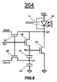
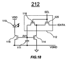
- 画素回路であって、
発光デバイスと、
ゲート端子、前記発光デバイスに結合される第1端子、および電圧供給ラインに結合される第2端子を有し、画素電流を前記発光デバイスへ供給するための駆動トランジスタと、
一端がプログラミング電圧を供給するためのデータ・ラインと直接に接続され、他端が前記駆動トランジスタの前記ゲート端子と接続されるストレージ・キャパシタと、
前記駆動トランジスタの前記ゲート端子と前記駆動トランジスタの前記第1端子との間に結合される第1スイッチ・トランジスタと、
プログラミング・サイクル中に、制御可能なバイアス電流を前記駆動トランジスタの前記第1端子へ供給するために、バイアス・ラインと前記駆動トランジスタの前記第1端子との間に結合される第2スイッチ・トランジスタと、
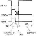
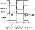
前記第1スイッチ・トランジスタおよび前記第2スイッチ・トランジスタと結合される制御回路であって、プログラミング・サイクルにおける選択された間隔の間に、前記第1スイッチ・トランジスタおよび前記第2スイッチ・トランジスタをオンにして、前記プログラミング電圧を前記ストレージ・キャパシタへ供給し、駆動サイクルの間に前記第1スイッチ・トランジスタおよび前記第2スイッチ・トランジスタをオフにして、駆動電流が前記駆動トランジスタおよび前記発光デバイスを通して流れるようにする、制御回路と
を備える画素回路。 - 請求項1に記載の画素回路であって、
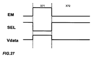
前記画素回路はディスプレイ装置に含まれるものであり、前記ディスプレイ装置はドライバ回路を含み、前記ドライバ回路は、プログラミング・サイクル中に前記画素回路をプログラムするためのものであり、前記プログラミング・サイクル中に、前記画素回路はプログラミング・データに応じたプログラミング電圧を受けるものであり、かつ、前記ドライバ回路は、駆動サイクル中に前記画素回路を駆動するためのものであり、前記駆動サイクル中に、前記画素回路は前記プログラミング・データに従った光を発するものであり、
前記ドライバ回路は、前記プログラミング・サイクル中に前記データ・ラインへ前記プログラミング電圧を供給し、前記プログラミング・サイクル中に前記バイアス・ラインへ前記制御可能なバイアス電流を供給し、前記制御可能なバイアス電流が前記駆動トランジスタを通るときに前記駆動トランジスタの前記ゲート端子が自己調整することを可能とすることにより、前記画素回路の時間依存性のパラメータを補償するように、構成される、
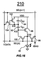
画素回路。 - 請求項2に記載の画素回路であって、前記制御可能なバイアス電流は、前記画素回路に対する前記プログラミング・データからは独立したものである、画素回路。
- 請求項1に記載の画素回路であって、前記第1スイッチ・トランジスタのゲート端子および前記第2スイッチ・トランジスタのゲート端子が、単一の選択ラインにより動作させられる、画素回路。
- 請求項1に記載の画素回路であって、前記第2スイッチ・トランジスタが、前記バイアス・ラインに結合された第1端子と、前記発光デバイスと前記駆動トランジスタとの間の接続ノードに結合された第2端子とを含む、画素回路。
- 請求項1に記載の画素回路であって、前記発光デバイスが有機発光ダイオードを含む、画素回路。
- 請求項1に記載の画素回路であって、前記トランジスタのうちの少なくとも1つが薄膜トランジスタである、画素回路。
- 請求項1に記載の画素回路であって、前記画素回路がアクティブ・マトリクス・アレイを形成する、画素回路。
Applications Claiming Priority (3)
| Application Number | Priority Date | Filing Date | Title |
|---|---|---|---|
| US4625608P | 2008-04-18 | 2008-04-18 | |
| US61/046,256 | 2008-04-18 | ||
| PCT/CA2009/000502 WO2009127065A1 (en) | 2008-04-18 | 2009-04-17 | System and driving method for light emitting device display |
Related Child Applications (1)
| Application Number | Title | Priority Date | Filing Date |
|---|---|---|---|
| JP2013169044A Division JP5726247B2 (ja) | 2008-04-18 | 2013-08-16 | 画素回路 |
Publications (3)
| Publication Number | Publication Date |
|---|---|
| JP2011520139A JP2011520139A (ja) | 2011-07-14 |
| JP2011520139A5 JP2011520139A5 (ja) | 2012-06-07 |
| JP5466694B2 true JP5466694B2 (ja) | 2014-04-09 |
Family
ID=40848360
Family Applications (2)
| Application Number | Title | Priority Date | Filing Date |
|---|---|---|---|
| JP2011504297A Active JP5466694B2 (ja) | 2008-04-18 | 2009-04-17 | 発光デバイス・ディスプレイのためのシステムおよび駆動方法 |
| JP2013169044A Active JP5726247B2 (ja) | 2008-04-18 | 2013-08-16 | 画素回路 |
Family Applications After (1)
| Application Number | Title | Priority Date | Filing Date |
|---|---|---|---|
| JP2013169044A Active JP5726247B2 (ja) | 2008-04-18 | 2013-08-16 | 画素回路 |
Country Status (8)
| Country | Link |
|---|---|
| US (4) | US8614652B2 (ja) |
| EP (1) | EP2277163B1 (ja) |
| JP (2) | JP5466694B2 (ja) |
| KR (1) | KR20100134125A (ja) |
| CN (2) | CN104299566B (ja) |
| CA (1) | CA2660598A1 (ja) |
| TW (1) | TW200949807A (ja) |
| WO (1) | WO2009127065A1 (ja) |
Families Citing this family (121)
| Publication number | Priority date | Publication date | Assignee | Title |
|---|---|---|---|---|
| CA2443206A1 (en) | 2003-09-23 | 2005-03-23 | Ignis Innovation Inc. | Amoled display backplanes - pixel driver circuits, array architecture, and external compensation |
| CA2490858A1 (en) | 2004-12-07 | 2006-06-07 | Ignis Innovation Inc. | Driving method for compensated voltage-programming of amoled displays |
| US8576217B2 (en) | 2011-05-20 | 2013-11-05 | Ignis Innovation Inc. | System and methods for extraction of threshold and mobility parameters in AMOLED displays |
| US10013907B2 (en) | 2004-12-15 | 2018-07-03 | Ignis Innovation Inc. | Method and system for programming, calibrating and/or compensating, and driving an LED display |
| US9799246B2 (en) | 2011-05-20 | 2017-10-24 | Ignis Innovation Inc. | System and methods for extraction of threshold and mobility parameters in AMOLED displays |
| US9280933B2 (en) | 2004-12-15 | 2016-03-08 | Ignis Innovation Inc. | System and methods for extraction of threshold and mobility parameters in AMOLED displays |
| EP2688058A3 (en) | 2004-12-15 | 2014-12-10 | Ignis Innovation Inc. | Method and system for programming, calibrating and driving a light emitting device display |
| US10012678B2 (en) | 2004-12-15 | 2018-07-03 | Ignis Innovation Inc. | Method and system for programming, calibrating and/or compensating, and driving an LED display |
| US9275579B2 (en) | 2004-12-15 | 2016-03-01 | Ignis Innovation Inc. | System and methods for extraction of threshold and mobility parameters in AMOLED displays |
| KR20080032072A (ko) | 2005-06-08 | 2008-04-14 | 이그니스 이노베이션 인크. | 발광 디바이스 디스플레이 구동 방법 및 시스템 |
| CA2518276A1 (en) | 2005-09-13 | 2007-03-13 | Ignis Innovation Inc. | Compensation technique for luminance degradation in electro-luminance devices |
| WO2007079572A1 (en) | 2006-01-09 | 2007-07-19 | Ignis Innovation Inc. | Method and system for driving an active matrix display circuit |
| US9269322B2 (en) | 2006-01-09 | 2016-02-23 | Ignis Innovation Inc. | Method and system for driving an active matrix display circuit |
| US9489891B2 (en) | 2006-01-09 | 2016-11-08 | Ignis Innovation Inc. | Method and system for driving an active matrix display circuit |
| US8477121B2 (en) | 2006-04-19 | 2013-07-02 | Ignis Innovation, Inc. | Stable driving scheme for active matrix displays |
| CA2556961A1 (en) | 2006-08-15 | 2008-02-15 | Ignis Innovation Inc. | Oled compensation technique based on oled capacitance |
| CN104299566B (zh) | 2008-04-18 | 2017-11-10 | 伊格尼斯创新公司 | 用于发光器件显示器的系统和驱动方法 |
| CA2637343A1 (en) | 2008-07-29 | 2010-01-29 | Ignis Innovation Inc. | Improving the display source driver |
| KR101502070B1 (ko) * | 2008-12-02 | 2015-03-12 | 삼성디스플레이 주식회사 | 표시 장치 및 그의 구동 방법 |
| US9370075B2 (en) | 2008-12-09 | 2016-06-14 | Ignis Innovation Inc. | System and method for fast compensation programming of pixels in a display |
| TWI393115B (zh) * | 2008-12-31 | 2013-04-11 | Princeton Technology Corp | 顯示器驅動電路及調整顯示器輸出亮度的方法 |
| US10319307B2 (en) | 2009-06-16 | 2019-06-11 | Ignis Innovation Inc. | Display system with compensation techniques and/or shared level resources |
| CA2688870A1 (en) | 2009-11-30 | 2011-05-30 | Ignis Innovation Inc. | Methode and techniques for improving display uniformity |
| US9384698B2 (en) | 2009-11-30 | 2016-07-05 | Ignis Innovation Inc. | System and methods for aging compensation in AMOLED displays |
| US9311859B2 (en) | 2009-11-30 | 2016-04-12 | Ignis Innovation Inc. | Resetting cycle for aging compensation in AMOLED displays |
| CA2669367A1 (en) | 2009-06-16 | 2010-12-16 | Ignis Innovation Inc | Compensation technique for color shift in displays |
| US8497828B2 (en) | 2009-11-12 | 2013-07-30 | Ignis Innovation Inc. | Sharing switch TFTS in pixel circuits |
| US10996258B2 (en) | 2009-11-30 | 2021-05-04 | Ignis Innovation Inc. | Defect detection and correction of pixel circuits for AMOLED displays |
| US8803417B2 (en) | 2009-12-01 | 2014-08-12 | Ignis Innovation Inc. | High resolution pixel architecture |
| CA2687631A1 (en) | 2009-12-06 | 2011-06-06 | Ignis Innovation Inc | Low power driving scheme for display applications |
| US20140313111A1 (en) | 2010-02-04 | 2014-10-23 | Ignis Innovation Inc. | System and methods for extracting correlation curves for an organic light emitting device |
| US9881532B2 (en) | 2010-02-04 | 2018-01-30 | Ignis Innovation Inc. | System and method for extracting correlation curves for an organic light emitting device |
| US10089921B2 (en) | 2010-02-04 | 2018-10-02 | Ignis Innovation Inc. | System and methods for extracting correlation curves for an organic light emitting device |
| US10176736B2 (en) | 2010-02-04 | 2019-01-08 | Ignis Innovation Inc. | System and methods for extracting correlation curves for an organic light emitting device |
| US10163401B2 (en) | 2010-02-04 | 2018-12-25 | Ignis Innovation Inc. | System and methods for extracting correlation curves for an organic light emitting device |
| CA2692097A1 (en) | 2010-02-04 | 2011-08-04 | Ignis Innovation Inc. | Extracting correlation curves for light emitting device |
| JP2011170616A (ja) * | 2010-02-18 | 2011-09-01 | On Semiconductor Trading Ltd | 静電容量型タッチセンサ |
| CA2696778A1 (en) | 2010-03-17 | 2011-09-17 | Ignis Innovation Inc. | Lifetime, uniformity, parameter extraction methods |
| US8907991B2 (en) | 2010-12-02 | 2014-12-09 | Ignis Innovation Inc. | System and methods for thermal compensation in AMOLED displays |
| GB2488178A (en) * | 2011-02-21 | 2012-08-22 | Cambridge Display Tech Ltd | Pixel driver circuitry for active matrix OLED display |
| US9886899B2 (en) | 2011-05-17 | 2018-02-06 | Ignis Innovation Inc. | Pixel Circuits for AMOLED displays |
| US9351368B2 (en) | 2013-03-08 | 2016-05-24 | Ignis Innovation Inc. | Pixel circuits for AMOLED displays |
| US20140368491A1 (en) | 2013-03-08 | 2014-12-18 | Ignis Innovation Inc. | Pixel circuits for amoled displays |
| US9530349B2 (en) | 2011-05-20 | 2016-12-27 | Ignis Innovations Inc. | Charged-based compensation and parameter extraction in AMOLED displays |
| US9466240B2 (en) | 2011-05-26 | 2016-10-11 | Ignis Innovation Inc. | Adaptive feedback system for compensating for aging pixel areas with enhanced estimation speed |
| CN106910464B (zh) * | 2011-05-27 | 2020-04-24 | 伊格尼斯创新公司 | 补偿显示器阵列中像素的系统和驱动发光器件的像素电路 |
| EP2945147B1 (en) | 2011-05-28 | 2018-08-01 | Ignis Innovation Inc. | Method for fast compensation programming of pixels in a display |
| US20120306391A1 (en) * | 2011-06-03 | 2012-12-06 | Taiwan Semiconductor Manufacturing Company, Ltd. | Modulized Full Operation Junction Ultra High Voltage (UHV) Device |
| KR102378948B1 (ko) | 2011-07-22 | 2022-03-24 | 가부시키가이샤 한도오따이 에네루기 켄큐쇼 | 발광 장치 |
| KR101960971B1 (ko) * | 2011-08-05 | 2019-03-21 | 가부시키가이샤 한도오따이 에네루기 켄큐쇼 | 표시 장치 |
| CN103403787B (zh) * | 2011-08-09 | 2016-06-29 | 株式会社日本有机雷特显示器 | 图像显示装置 |
| JP5909759B2 (ja) * | 2011-09-07 | 2016-04-27 | 株式会社Joled | 画素回路、表示パネル、表示装置および電子機器 |
| JP5779656B2 (ja) * | 2011-10-14 | 2015-09-16 | 株式会社Joled | 画像表示装置 |
| US9324268B2 (en) | 2013-03-15 | 2016-04-26 | Ignis Innovation Inc. | Amoled displays with multiple readout circuits |
| US10089924B2 (en) | 2011-11-29 | 2018-10-02 | Ignis Innovation Inc. | Structural and low-frequency non-uniformity compensation |
| KR101928433B1 (ko) | 2012-01-09 | 2019-02-26 | 삼성전자주식회사 | 반사형 디스플레이 장치 |
| US8937632B2 (en) | 2012-02-03 | 2015-01-20 | Ignis Innovation Inc. | Driving system for active-matrix displays |
| EP2842392B1 (en) | 2012-04-23 | 2018-08-15 | Koninklijke Philips N.V. | Separately controllable array of radiation elements |
| US9747834B2 (en) | 2012-05-11 | 2017-08-29 | Ignis Innovation Inc. | Pixel circuits including feedback capacitors and reset capacitors, and display systems therefore |
| US8922544B2 (en) | 2012-05-23 | 2014-12-30 | Ignis Innovation Inc. | Display systems with compensation for line propagation delay |
| US20140002332A1 (en) * | 2012-06-29 | 2014-01-02 | Taiwan Semiconductor Manufacturing Company, Ltd. | Pixels for display |
| US9336717B2 (en) | 2012-12-11 | 2016-05-10 | Ignis Innovation Inc. | Pixel circuits for AMOLED displays |
| US9786223B2 (en) | 2012-12-11 | 2017-10-10 | Ignis Innovation Inc. | Pixel circuits for AMOLED displays |
| US9830857B2 (en) | 2013-01-14 | 2017-11-28 | Ignis Innovation Inc. | Cleaning common unwanted signals from pixel measurements in emissive displays |
| DE112014000422T5 (de) | 2013-01-14 | 2015-10-29 | Ignis Innovation Inc. | Ansteuerschema für Emissionsanzeigen, das eine Kompensation für Ansteuertransistorschwankungen bereitstellt |
| CA2894717A1 (en) | 2015-06-19 | 2016-12-19 | Ignis Innovation Inc. | Optoelectronic device characterization in array with shared sense line |
| US9721505B2 (en) | 2013-03-08 | 2017-08-01 | Ignis Innovation Inc. | Pixel circuits for AMOLED displays |
| EP2779147B1 (en) | 2013-03-14 | 2016-03-02 | Ignis Innovation Inc. | Re-interpolation with edge detection for extracting an aging pattern for AMOLED displays |
| CN110634431B (zh) | 2013-04-22 | 2023-04-18 | 伊格尼斯创新公司 | 检测和制造显示面板的方法 |
| CN103400548B (zh) * | 2013-07-31 | 2016-03-16 | 京东方科技集团股份有限公司 | 像素驱动电路及其驱动方法、显示装置 |
| DE112014003719T5 (de) | 2013-08-12 | 2016-05-19 | Ignis Innovation Inc. | Kompensationsgenauigkeit |
| JP6142178B2 (ja) * | 2013-09-04 | 2017-06-07 | 株式会社Joled | 表示装置および駆動方法 |
| US9741282B2 (en) | 2013-12-06 | 2017-08-22 | Ignis Innovation Inc. | OLED display system and method |
| US9761170B2 (en) | 2013-12-06 | 2017-09-12 | Ignis Innovation Inc. | Correction for localized phenomena in an image array |
| US9502653B2 (en) | 2013-12-25 | 2016-11-22 | Ignis Innovation Inc. | Electrode contacts |
| CN117690933A (zh) | 2013-12-27 | 2024-03-12 | 株式会社半导体能源研究所 | 发光装置 |
| JP6506961B2 (ja) | 2013-12-27 | 2019-04-24 | 株式会社半導体エネルギー研究所 | 液晶表示装置 |
| US9870060B2 (en) * | 2013-12-31 | 2018-01-16 | Google Llc | Systems and methods for gaze-based media selection and editing |
| US9343012B2 (en) * | 2013-12-31 | 2016-05-17 | Shenzhen China Star Optoelectronics Technology Co., Ltd | Driving circuit of AMOLED and method for driving the AMOLED |
| US10192479B2 (en) | 2014-04-08 | 2019-01-29 | Ignis Innovation Inc. | Display system using system level resources to calculate compensation parameters for a display module in a portable device |
| JP6528267B2 (ja) | 2014-06-27 | 2019-06-12 | Tianma Japan株式会社 | 画素回路及びその駆動方法 |
| CA2873476A1 (en) | 2014-12-08 | 2016-06-08 | Ignis Innovation Inc. | Smart-pixel display architecture |
| CN104599630B (zh) * | 2014-12-16 | 2017-04-19 | 上海天马有机发光显示技术有限公司 | 一种驱动电路及发光控制电路、显示面板、显示装置 |
| CA2879462A1 (en) | 2015-01-23 | 2016-07-23 | Ignis Innovation Inc. | Compensation for color variation in emissive devices |
| CN104658485B (zh) * | 2015-03-24 | 2017-03-29 | 京东方科技集团股份有限公司 | Oled驱动补偿电路及其驱动方法 |
| CA2886862A1 (en) | 2015-04-01 | 2016-10-01 | Ignis Innovation Inc. | Adjusting display brightness for avoiding overheating and/or accelerated aging |
| CA2889870A1 (en) | 2015-05-04 | 2016-11-04 | Ignis Innovation Inc. | Optical feedback system |
| CA2892714A1 (en) | 2015-05-27 | 2016-11-27 | Ignis Innovation Inc | Memory bandwidth reduction in compensation system |
| CA2898282A1 (en) | 2015-07-24 | 2017-01-24 | Ignis Innovation Inc. | Hybrid calibration of current sources for current biased voltage progra mmed (cbvp) displays |
| US10657895B2 (en) | 2015-07-24 | 2020-05-19 | Ignis Innovation Inc. | Pixels and reference circuits and timing techniques |
| US10373554B2 (en) | 2015-07-24 | 2019-08-06 | Ignis Innovation Inc. | Pixels and reference circuits and timing techniques |
| CA2900170A1 (en) | 2015-08-07 | 2017-02-07 | Gholamreza Chaji | Calibration of pixel based on improved reference values |
| CN105139802A (zh) * | 2015-09-10 | 2015-12-09 | 中国科学院上海高等研究院 | 电压电流混合编程的amoled像素驱动电路及方法 |
| CA2908285A1 (en) | 2015-10-14 | 2017-04-14 | Ignis Innovation Inc. | Driver with multiple color pixel structure |
| CN105577140B (zh) * | 2015-12-14 | 2018-02-06 | 上海华虹宏力半导体制造有限公司 | 晶振驱动电路 |
| CN105609050B (zh) | 2016-01-04 | 2018-03-06 | 京东方科技集团股份有限公司 | 像素补偿电路及amoled显示装置 |
| CN105575327B (zh) * | 2016-03-21 | 2018-03-16 | 京东方科技集团股份有限公司 | 一种像素电路、其驱动方法及有机电致发光显示面板 |
| EP3264544B1 (en) * | 2016-06-28 | 2020-01-01 | ams AG | Driving circuit to generate a signal pulse for operating a light-emitting diode |
| CN107958653B (zh) * | 2016-10-18 | 2021-02-02 | 京东方科技集团股份有限公司 | 阵列基板及其驱动方法、驱动电路及显示装置 |
| KR101856378B1 (ko) * | 2016-10-31 | 2018-06-20 | 엘지디스플레이 주식회사 | 유기 발광 표시 장치 및 그의 구동 방법 |
| KR102617966B1 (ko) | 2016-12-28 | 2023-12-28 | 엘지디스플레이 주식회사 | 전계 발광 표시 장치와 그 구동 방법 |
| CN106782332B (zh) * | 2017-01-19 | 2019-03-05 | 上海天马有机发光显示技术有限公司 | 有机发光显示面板及其驱动方法、有机发光显示装置 |
| CN106910466A (zh) | 2017-04-28 | 2017-06-30 | 深圳市华星光电技术有限公司 | 像素驱动电路、显示面板及像素驱动方法 |
| US10460664B2 (en) * | 2017-05-02 | 2019-10-29 | Shenzhen China Star Technology Co., Ltd | Pixel compensation circuit, scanning driving circuit and display device |
| CN106940981A (zh) * | 2017-05-04 | 2017-07-11 | 成都晶砂科技有限公司 | 单晶硅晶体管cmos驱动显示的像素补偿电路及显示设备 |
| CN107369410B (zh) * | 2017-08-31 | 2023-11-21 | 京东方科技集团股份有限公司 | 像素电路、驱动方法和显示装置 |
| CN110010066B (zh) * | 2017-11-22 | 2023-08-15 | 伊格尼斯创新公司 | 像素电路、显示器和方法 |
| TWI662348B (zh) * | 2018-01-05 | 2019-06-11 | 友達光電股份有限公司 | 像素電路及顯示裝置 |
| CN108538242A (zh) * | 2018-01-26 | 2018-09-14 | 上海天马有机发光显示技术有限公司 | 像素驱动电路及其驱动方法、显示面板和显示装置 |
| CN108364959A (zh) * | 2018-02-11 | 2018-08-03 | 武汉华星光电半导体显示技术有限公司 | Oled面板制作方法 |
| US20190371244A1 (en) * | 2018-05-30 | 2019-12-05 | Viewtrix Technology Co., Ltd. | Pixel circuits for light emitting elements |
| TWI685831B (zh) * | 2019-01-08 | 2020-02-21 | 友達光電股份有限公司 | 畫素電路及其驅動方法 |
| CN109741708A (zh) * | 2019-02-26 | 2019-05-10 | 深圳市华星光电半导体显示技术有限公司 | 像素驱动电路及显示面板 |
| TWI703544B (zh) * | 2019-02-27 | 2020-09-01 | 友達光電股份有限公司 | 像素電路與其驅動方法 |
| KR20210010344A (ko) * | 2019-07-16 | 2021-01-27 | 삼성디스플레이 주식회사 | 표시 장치 및 이의 구동 방법 |
| TWI709953B (zh) * | 2019-10-02 | 2020-11-11 | 友達光電股份有限公司 | 畫素陣列 |
| CN111754921B (zh) * | 2020-07-24 | 2023-09-26 | 武汉华星光电半导体显示技术有限公司 | 像素电路 |
| TW202211195A (zh) * | 2020-08-12 | 2022-03-16 | 日商半導體能源研究所股份有限公司 | 顯示裝置、其工作方法以及電子裝置 |
| CN112309320A (zh) * | 2020-11-05 | 2021-02-02 | 重庆惠科金渝光电科技有限公司 | 显示面板驱动电路及显示装置 |
| CN113078174B (zh) * | 2021-04-13 | 2022-08-12 | 厦门天马微电子有限公司 | 阵列基板、显示面板及显示装置 |
| CN113299235B (zh) * | 2021-05-20 | 2022-10-25 | 京东方科技集团股份有限公司 | 像素电路及其驱动方法、显示装置 |
Family Cites Families (369)
| Publication number | Priority date | Publication date | Assignee | Title |
|---|---|---|---|---|
| AU153946B2 (en) | 1952-01-08 | 1953-11-03 | Maatschappij Voor Kolenbewerking Stamicarbon N. V | Multi hydrocyclone or multi vortex chamber and method of treating a suspension therein |
| US3506851A (en) | 1966-12-14 | 1970-04-14 | North American Rockwell | Field effect transistor driver using capacitor feedback |
| DE2039669C3 (de) | 1970-08-10 | 1978-11-02 | Klaus 5500 Trier Goebel | Im Bereich einer Fugenkreuzung einer Plattenlage angeordnetes Lager zum Aufständern der Platten |
| US3774055A (en) | 1972-01-24 | 1973-11-20 | Nat Semiconductor Corp | Clocked bootstrap inverter circuit |
| JPS52119160A (en) | 1976-03-31 | 1977-10-06 | Nec Corp | Semiconductor circuit with insulating gate type field dffect transisto r |
| US4354162A (en) | 1981-02-09 | 1982-10-12 | National Semiconductor Corporation | Wide dynamic range control amplifier with offset correction |
| JPS61161093A (ja) | 1985-01-09 | 1986-07-21 | Sony Corp | ダイナミツクユニフオミテイ補正装置 |
| US4996523A (en) | 1988-10-20 | 1991-02-26 | Eastman Kodak Company | Electroluminescent storage display with improved intensity driver circuits |
| US5170158A (en) | 1989-06-30 | 1992-12-08 | Kabushiki Kaisha Toshiba | Display apparatus |
| US5134387A (en) | 1989-11-06 | 1992-07-28 | Texas Digital Systems, Inc. | Multicolor display system |
| GB9020892D0 (en) | 1990-09-25 | 1990-11-07 | Emi Plc Thorn | Improvements in or relating to display devices |
| US5153420A (en) | 1990-11-28 | 1992-10-06 | Xerox Corporation | Timing independent pixel-scale light sensing apparatus |
| US5204661A (en) | 1990-12-13 | 1993-04-20 | Xerox Corporation | Input/output pixel circuit and array of such circuits |
| US5589847A (en) | 1991-09-23 | 1996-12-31 | Xerox Corporation | Switched capacitor analog circuits using polysilicon thin film technology |
| US5266515A (en) | 1992-03-02 | 1993-11-30 | Motorola, Inc. | Fabricating dual gate thin film transistors |
| US5572444A (en) | 1992-08-19 | 1996-11-05 | Mtl Systems, Inc. | Method and apparatus for automatic performance evaluation of electronic display devices |
| JP3221085B2 (ja) * | 1992-09-14 | 2001-10-22 | 富士ゼロックス株式会社 | 並列処理装置 |
| CN1123577A (zh) | 1993-04-05 | 1996-05-29 | 西尔拉斯逻辑公司 | 液晶显示器中串扰的补偿方法和设备 |
| JPH0799321A (ja) | 1993-05-27 | 1995-04-11 | Sony Corp | 薄膜半導体素子の製造方法および製造装置 |
| JPH07120722A (ja) | 1993-06-30 | 1995-05-12 | Sharp Corp | 液晶表示素子およびその駆動方法 |
| US5408267A (en) | 1993-07-06 | 1995-04-18 | The 3Do Company | Method and apparatus for gamma correction by mapping, transforming and demapping |
| US5479606A (en) * | 1993-07-21 | 1995-12-26 | Pgm Systems, Inc. | Data display apparatus for displaying patterns using samples of signal data |
| JP3067949B2 (ja) | 1994-06-15 | 2000-07-24 | シャープ株式会社 | 電子装置および液晶表示装置 |
| US5714968A (en) | 1994-08-09 | 1998-02-03 | Nec Corporation | Current-dependent light-emitting element drive circuit for use in active matrix display device |
| US5498880A (en) | 1995-01-12 | 1996-03-12 | E. I. Du Pont De Nemours And Company | Image capture panel using a solid state device |
| US5745660A (en) | 1995-04-26 | 1998-04-28 | Polaroid Corporation | Image rendering system and method for generating stochastic threshold arrays for use therewith |
| US5619033A (en) | 1995-06-07 | 1997-04-08 | Xerox Corporation | Layered solid state photodiode sensor array |
| US5748160A (en) | 1995-08-21 | 1998-05-05 | Mororola, Inc. | Active driven LED matrices |
| JP3272209B2 (ja) | 1995-09-07 | 2002-04-08 | アルプス電気株式会社 | Lcd駆動回路 |
| JPH0990405A (ja) | 1995-09-21 | 1997-04-04 | Sharp Corp | 薄膜トランジスタ |
| US6694248B2 (en) | 1995-10-27 | 2004-02-17 | Total Technology Inc. | Fully automated vehicle dispatching, monitoring and billing |
| US7113864B2 (en) | 1995-10-27 | 2006-09-26 | Total Technology, Inc. | Fully automated vehicle dispatching, monitoring and billing |
| US5835376A (en) | 1995-10-27 | 1998-11-10 | Total Technology, Inc. | Fully automated vehicle dispatching, monitoring and billing |
| US5949398A (en) | 1996-04-12 | 1999-09-07 | Thomson Multimedia S.A. | Select line driver for a display matrix with toggling backplane |
| AU764896B2 (en) | 1996-08-30 | 2003-09-04 | Canon Kabushiki Kaisha | Mounting method for a combination solar battery and roof unit |
| JP3266177B2 (ja) | 1996-09-04 | 2002-03-18 | 住友電気工業株式会社 | 電流ミラー回路とそれを用いた基準電圧発生回路及び発光素子駆動回路 |
| US5783952A (en) | 1996-09-16 | 1998-07-21 | Atmel Corporation | Clock feedthrough reduction system for switched current memory cells |
| US5874803A (en) | 1997-09-09 | 1999-02-23 | The Trustees Of Princeton University | Light emitting device with stack of OLEDS and phosphor downconverter |
| TW441136B (en) | 1997-01-28 | 2001-06-16 | Casio Computer Co Ltd | An electroluminescent display device and a driving method thereof |
| US5917280A (en) | 1997-02-03 | 1999-06-29 | The Trustees Of Princeton University | Stacked organic light emitting devices |
| KR100509240B1 (ko) | 1997-02-17 | 2005-08-22 | 세이코 엡슨 가부시키가이샤 | 표시 장치 |
| JPH10254410A (ja) | 1997-03-12 | 1998-09-25 | Pioneer Electron Corp | 有機エレクトロルミネッセンス表示装置及びその駆動方法 |
| US5903248A (en) | 1997-04-11 | 1999-05-11 | Spatialight, Inc. | Active matrix display having pixel driving circuits with integrated charge pumps |
| US5952789A (en) | 1997-04-14 | 1999-09-14 | Sarnoff Corporation | Active matrix organic light emitting diode (amoled) display pixel structure and data load/illuminate circuit therefor |
| US6229506B1 (en) | 1997-04-23 | 2001-05-08 | Sarnoff Corporation | Active matrix light emitting diode pixel structure and concomitant method |
| KR100430091B1 (ko) | 1997-07-10 | 2004-07-15 | 엘지.필립스 엘시디 주식회사 | 액정표시장치 |
| US6023259A (en) | 1997-07-11 | 2000-02-08 | Fed Corporation | OLED active matrix using a single transistor current mode pixel design |
| KR100323441B1 (ko) | 1997-08-20 | 2002-06-20 | 윤종용 | 엠펙2동화상부호화/복호화시스템 |
| US20010043173A1 (en) | 1997-09-04 | 2001-11-22 | Ronald Roy Troutman | Field sequential gray in active matrix led display using complementary transistor pixel circuits |
| JPH1187720A (ja) | 1997-09-08 | 1999-03-30 | Sanyo Electric Co Ltd | 半導体装置及び液晶表示装置 |
| JP3229250B2 (ja) * | 1997-09-12 | 2001-11-19 | インターナショナル・ビジネス・マシーンズ・コーポレーション | 液晶表示装置における画像表示方法及び液晶表示装置 |
| US6100868A (en) | 1997-09-15 | 2000-08-08 | Silicon Image, Inc. | High density column drivers for an active matrix display |
| US6229508B1 (en) * | 1997-09-29 | 2001-05-08 | Sarnoff Corporation | Active matrix light emitting diode pixel structure and concomitant method |
| US6909419B2 (en) | 1997-10-31 | 2005-06-21 | Kopin Corporation | Portable microdisplay system |
| US6069365A (en) | 1997-11-25 | 2000-05-30 | Alan Y. Chow | Optical processor based imaging system |
| GB2333174A (en) | 1998-01-09 | 1999-07-14 | Sharp Kk | Data line driver for an active matrix display |
| JPH11231805A (ja) | 1998-02-10 | 1999-08-27 | Sanyo Electric Co Ltd | 表示装置 |
| JP3595153B2 (ja) | 1998-03-03 | 2004-12-02 | 株式会社 日立ディスプレイズ | 液晶表示装置および映像信号線駆動手段 |
| US6097360A (en) | 1998-03-19 | 2000-08-01 | Holloman; Charles J | Analog driver for LED or similar display element |
| JP3252897B2 (ja) | 1998-03-31 | 2002-02-04 | 日本電気株式会社 | 素子駆動装置および方法、画像表示装置 |
| JP3702096B2 (ja) | 1998-06-08 | 2005-10-05 | 三洋電機株式会社 | 薄膜トランジスタ及び表示装置 |
| CA2242720C (en) | 1998-07-09 | 2000-05-16 | Ibm Canada Limited-Ibm Canada Limitee | Programmable led driver |
| US6417825B1 (en) | 1998-09-29 | 2002-07-09 | Sarnoff Corporation | Analog active matrix emissive display |
| US6473065B1 (en) * | 1998-11-16 | 2002-10-29 | Nongqiang Fan | Methods of improving display uniformity of organic light emitting displays by calibrating individual pixel |
| US6501098B2 (en) | 1998-11-25 | 2002-12-31 | Semiconductor Energy Laboratory Co, Ltd. | Semiconductor device |
| JP3423232B2 (ja) | 1998-11-30 | 2003-07-07 | 三洋電機株式会社 | アクティブ型el表示装置 |
| JP3031367B1 (ja) | 1998-12-02 | 2000-04-10 | 日本電気株式会社 | イメージセンサ |
| JP2000174282A (ja) | 1998-12-03 | 2000-06-23 | Semiconductor Energy Lab Co Ltd | 半導体装置 |
| KR20020006019A (ko) | 1998-12-14 | 2002-01-18 | 도날드 피. 게일 | 휴대용 마이크로디스플레이 시스템 |
| US6639244B1 (en) | 1999-01-11 | 2003-10-28 | Semiconductor Energy Laboratory Co., Ltd. | Semiconductor device and method of fabricating the same |
| JP3686769B2 (ja) | 1999-01-29 | 2005-08-24 | 日本電気株式会社 | 有機el素子駆動装置と駆動方法 |
| JP2000231346A (ja) | 1999-02-09 | 2000-08-22 | Sanyo Electric Co Ltd | エレクトロルミネッセンス表示装置 |
| US7122835B1 (en) | 1999-04-07 | 2006-10-17 | Semiconductor Energy Laboratory Co., Ltd. | Electrooptical device and a method of manufacturing the same |
| JP4565700B2 (ja) | 1999-05-12 | 2010-10-20 | ルネサスエレクトロニクス株式会社 | 半導体装置 |
| KR100296113B1 (ko) | 1999-06-03 | 2001-07-12 | 구본준, 론 위라하디락사 | 전기발광소자 |
| JP3556150B2 (ja) | 1999-06-15 | 2004-08-18 | シャープ株式会社 | 液晶表示方法および液晶表示装置 |
| JP4627822B2 (ja) | 1999-06-23 | 2011-02-09 | 株式会社半導体エネルギー研究所 | 表示装置 |
| JP4126909B2 (ja) | 1999-07-14 | 2008-07-30 | ソニー株式会社 | 電流駆動回路及びそれを用いた表示装置、画素回路、並びに駆動方法 |
| JP2003509728A (ja) | 1999-09-11 | 2003-03-11 | コーニンクレッカ フィリップス エレクトロニクス エヌ ヴィ | アクティブマトリックスelディスプレイ装置 |
| JP4686800B2 (ja) | 1999-09-28 | 2011-05-25 | 三菱電機株式会社 | 画像表示装置 |
| KR20010080746A (ko) | 1999-10-12 | 2001-08-22 | 요트.게.아. 롤페즈 | Led 디스플레이 디바이스 |
| US6392617B1 (en) | 1999-10-27 | 2002-05-21 | Agilent Technologies, Inc. | Active matrix light emitting diode display |
| JP2001147659A (ja) * | 1999-11-18 | 2001-05-29 | Sony Corp | 表示装置 |
| TW587239B (en) | 1999-11-30 | 2004-05-11 | Semiconductor Energy Lab | Electric device |
| GB9929501D0 (en) | 1999-12-14 | 2000-02-09 | Koninkl Philips Electronics Nv | Image sensor |
| US6307322B1 (en) | 1999-12-28 | 2001-10-23 | Sarnoff Corporation | Thin-film transistor circuitry with reduced sensitivity to variance in transistor threshold voltage |
| WO2001054107A1 (en) | 2000-01-21 | 2001-07-26 | Emagin Corporation | Gray scale pixel driver for electronic display and method of operation therefor |
| US6639265B2 (en) | 2000-01-26 | 2003-10-28 | Semiconductor Energy Laboratory Co., Ltd. | Semiconductor device and method of manufacturing the semiconductor device |
| US7030921B2 (en) | 2000-02-01 | 2006-04-18 | Minolta Co., Ltd. | Solid-state image-sensing device |
| US6414661B1 (en) * | 2000-02-22 | 2002-07-02 | Sarnoff Corporation | Method and apparatus for calibrating display devices and automatically compensating for loss in their efficiency over time |
| KR100327374B1 (ko) * | 2000-03-06 | 2002-03-06 | 구자홍 | 액티브 구동 회로 |
| TW521226B (en) | 2000-03-27 | 2003-02-21 | Semiconductor Energy Lab | Electro-optical device |
| JP2001284592A (ja) | 2000-03-29 | 2001-10-12 | Sony Corp | 薄膜半導体装置及びその駆動方法 |
| US6528950B2 (en) | 2000-04-06 | 2003-03-04 | Semiconductor Energy Laboratory Co., Ltd. | Electronic device and driving method |
| US6583576B2 (en) | 2000-05-08 | 2003-06-24 | Semiconductor Energy Laboratory Co., Ltd. | Light-emitting device, and electric device using the same |
| EP1158483A3 (en) | 2000-05-24 | 2003-02-05 | Eastman Kodak Company | Solid-state display with reference pixel |
| JP4703815B2 (ja) | 2000-05-26 | 2011-06-15 | 株式会社半導体エネルギー研究所 | Mos型センサの駆動方法、及び撮像方法 |
| TW503565B (en) | 2000-06-22 | 2002-09-21 | Semiconductor Energy Lab | Display device |
| JP3437152B2 (ja) | 2000-07-28 | 2003-08-18 | ウインテスト株式会社 | 有機elディスプレイの評価装置および評価方法 |
| US6828950B2 (en) | 2000-08-10 | 2004-12-07 | Semiconductor Energy Laboratory Co., Ltd. | Display device and method of driving the same |
| US7008904B2 (en) | 2000-09-13 | 2006-03-07 | Monsanto Technology, Llc | Herbicidal compositions containing glyphosate and bipyridilium |
| US7315295B2 (en) | 2000-09-29 | 2008-01-01 | Seiko Epson Corporation | Driving method for electro-optical device, electro-optical device, and electronic apparatus |
| JP2002162934A (ja) | 2000-09-29 | 2002-06-07 | Eastman Kodak Co | 発光フィードバックのフラットパネルディスプレイ |
| JP4925528B2 (ja) | 2000-09-29 | 2012-04-25 | 三洋電機株式会社 | 表示装置 |
| US6781567B2 (en) | 2000-09-29 | 2004-08-24 | Seiko Epson Corporation | Driving method for electro-optical device, electro-optical device, and electronic apparatus |
| JP2002123226A (ja) | 2000-10-12 | 2002-04-26 | Hitachi Ltd | 液晶表示装置 |
| TW550530B (en) | 2000-10-27 | 2003-09-01 | Semiconductor Energy Lab | Display device and method of driving the same |
| JP2002141420A (ja) | 2000-10-31 | 2002-05-17 | Mitsubishi Electric Corp | 半導体装置及びその製造方法 |
| KR100405026B1 (ko) | 2000-12-22 | 2003-11-07 | 엘지.필립스 엘시디 주식회사 | 액정표시장치 |
| TW518532B (en) | 2000-12-26 | 2003-01-21 | Hannstar Display Corp | Driving circuit of gate control line and method |
| TW561445B (en) * | 2001-01-02 | 2003-11-11 | Chi Mei Optoelectronics Corp | OLED active driving system with current feedback |
| US6580657B2 (en) | 2001-01-04 | 2003-06-17 | International Business Machines Corporation | Low-power organic light emitting diode pixel circuit |
| JP3593982B2 (ja) | 2001-01-15 | 2004-11-24 | ソニー株式会社 | アクティブマトリクス型表示装置およびアクティブマトリクス型有機エレクトロルミネッセンス表示装置、並びにそれらの駆動方法 |
| US6323631B1 (en) | 2001-01-18 | 2001-11-27 | Sunplus Technology Co., Ltd. | Constant current driver with auto-clamped pre-charge function |
| JP3639830B2 (ja) | 2001-02-05 | 2005-04-20 | インターナショナル・ビジネス・マシーンズ・コーポレーション | 液晶表示装置 |
| JP2002244617A (ja) | 2001-02-15 | 2002-08-30 | Sanyo Electric Co Ltd | 有機el画素回路 |
| CA2438577C (en) | 2001-02-16 | 2006-08-22 | Ignis Innovation Inc. | Pixel current driver for organic light emitting diode displays |
| JP4392165B2 (ja) | 2001-02-16 | 2009-12-24 | イグニス・イノベイション・インコーポレーテッド | 遮蔽電極を有する有機発光ダイオード表示器 |
| EP1488454B1 (en) * | 2001-02-16 | 2013-01-16 | Ignis Innovation Inc. | Pixel driver circuit for an organic light emitting diode |
| US7569849B2 (en) | 2001-02-16 | 2009-08-04 | Ignis Innovation Inc. | Pixel driver circuit and pixel circuit having the pixel driver circuit |
| US7061451B2 (en) | 2001-02-21 | 2006-06-13 | Semiconductor Energy Laboratory Co., Ltd, | Light emitting device and electronic device |
| JP2002278513A (ja) | 2001-03-19 | 2002-09-27 | Sharp Corp | 電気光学装置 |
| JPWO2002075710A1 (ja) * | 2001-03-21 | 2004-07-08 | キヤノン株式会社 | アクティブマトリクス型発光素子の駆動回路 |
| JP2002351401A (ja) * | 2001-03-21 | 2002-12-06 | Mitsubishi Electric Corp | 自発光型表示装置 |
| JPWO2002075709A1 (ja) * | 2001-03-21 | 2004-07-08 | キヤノン株式会社 | アクティブマトリクス型発光素子の駆動回路 |
| US7164417B2 (en) | 2001-03-26 | 2007-01-16 | Eastman Kodak Company | Dynamic controller for active-matrix displays |
| JP3862966B2 (ja) | 2001-03-30 | 2006-12-27 | 株式会社日立製作所 | 画像表示装置 |
| JP3819723B2 (ja) | 2001-03-30 | 2006-09-13 | 株式会社日立製作所 | 表示装置及びその駆動方法 |
| US7136058B2 (en) | 2001-04-27 | 2006-11-14 | Kabushiki Kaisha Toshiba | Display apparatus, digital-to-analog conversion circuit and digital-to-analog conversion method |
| JP4785271B2 (ja) | 2001-04-27 | 2011-10-05 | 株式会社半導体エネルギー研究所 | 液晶表示装置、電子機器 |
| JP2002351409A (ja) | 2001-05-23 | 2002-12-06 | Internatl Business Mach Corp <Ibm> | 液晶表示装置、液晶ディスプレイ駆動回路、液晶ディスプレイの駆動方法、およびプログラム |
| JP3610923B2 (ja) * | 2001-05-30 | 2005-01-19 | ソニー株式会社 | アクティブマトリクス型表示装置およびアクティブマトリクス型有機エレクトロルミネッセンス表示装置、並びにそれらの駆動方法 |
| JP3743387B2 (ja) | 2001-05-31 | 2006-02-08 | ソニー株式会社 | アクティブマトリクス型表示装置およびアクティブマトリクス型有機エレクトロルミネッセンス表示装置、並びにそれらの駆動方法 |
| US7012588B2 (en) | 2001-06-05 | 2006-03-14 | Eastman Kodak Company | Method for saving power in an organic electroluminescent display using white light emitting elements |
| KR100743103B1 (ko) | 2001-06-22 | 2007-07-27 | 엘지.필립스 엘시디 주식회사 | 일렉트로 루미네센스 패널 |
| WO2003001496A1 (en) * | 2001-06-22 | 2003-01-03 | Ibm Corporation | Oled current drive pixel circuit |
| HU225955B1 (en) | 2001-07-26 | 2008-01-28 | Egis Gyogyszergyar Nyilvanosan | Novel 2h-pyridazin-3-one derivatives, process for their preparation, their use and pharmaceutical compositions containing them |
| JP2003043994A (ja) | 2001-07-27 | 2003-02-14 | Canon Inc | アクティブマトリックス型ディスプレイ |
| JP3800050B2 (ja) * | 2001-08-09 | 2006-07-19 | 日本電気株式会社 | 表示装置の駆動回路 |
| CN101257743B (zh) | 2001-08-29 | 2011-05-25 | 株式会社半导体能源研究所 | 发光器件及这种发光器件的驱动方法 |
| US7209101B2 (en) * | 2001-08-29 | 2007-04-24 | Nec Corporation | Current load device and method for driving the same |
| JP2003076331A (ja) | 2001-08-31 | 2003-03-14 | Seiko Epson Corp | 表示装置および電子機器 |
| US7027015B2 (en) | 2001-08-31 | 2006-04-11 | Intel Corporation | Compensating organic light emitting device displays for color variations |
| JP4075505B2 (ja) | 2001-09-10 | 2008-04-16 | セイコーエプソン株式会社 | 電子回路、電子装置、及び電子機器 |
| WO2003027997A1 (fr) | 2001-09-21 | 2003-04-03 | Semiconductor Energy Laboratory Co., Ltd. | Ecran et procede de fonctionnement associe |
| JP2003099000A (ja) | 2001-09-25 | 2003-04-04 | Matsushita Electric Ind Co Ltd | 電流駆動型表示パネルの駆動方法、駆動回路及び表示装置 |
| JP3725458B2 (ja) | 2001-09-25 | 2005-12-14 | シャープ株式会社 | アクティブマトリクス表示パネル、およびそれを備えた画像表示装置 |
| JP4230744B2 (ja) | 2001-09-29 | 2009-02-25 | 東芝松下ディスプレイテクノロジー株式会社 | 表示装置 |
| JP3601499B2 (ja) | 2001-10-17 | 2004-12-15 | ソニー株式会社 | 表示装置 |
| AU2002348472A1 (en) | 2001-10-19 | 2003-04-28 | Clare Micronix Integrated Systems, Inc. | System and method for providing pulse amplitude modulation for oled display drivers |
| US20030169241A1 (en) | 2001-10-19 | 2003-09-11 | Lechevalier Robert E. | Method and system for ramp control of precharge voltage |
| US6861810B2 (en) | 2001-10-23 | 2005-03-01 | Fpd Systems | Organic electroluminescent display device driving method and apparatus |
| US7180479B2 (en) | 2001-10-30 | 2007-02-20 | Semiconductor Energy Laboratory Co., Ltd. | Signal line drive circuit and light emitting device and driving method therefor |
| KR100433216B1 (ko) | 2001-11-06 | 2004-05-27 | 엘지.필립스 엘시디 주식회사 | 일렉트로 루미네센스 패널의 구동장치 및 방법 |
| KR100940342B1 (ko) | 2001-11-13 | 2010-02-04 | 가부시키가이샤 한도오따이 에네루기 켄큐쇼 | 표시장치 및 그 구동방법 |
| TW518543B (en) | 2001-11-14 | 2003-01-21 | Ind Tech Res Inst | Integrated current driving framework of active matrix OLED |
| US7071932B2 (en) * | 2001-11-20 | 2006-07-04 | Toppoly Optoelectronics Corporation | Data voltage current drive amoled pixel circuit |
| TW529006B (en) | 2001-11-28 | 2003-04-21 | Ind Tech Res Inst | Array circuit of light emitting diode display |
| JP2003177709A (ja) | 2001-12-13 | 2003-06-27 | Seiko Epson Corp | 発光素子用の画素回路 |
| JP2003186437A (ja) * | 2001-12-18 | 2003-07-04 | Sanyo Electric Co Ltd | 表示装置 |
| JP3800404B2 (ja) | 2001-12-19 | 2006-07-26 | 株式会社日立製作所 | 画像表示装置 |
| GB0130411D0 (en) | 2001-12-20 | 2002-02-06 | Koninkl Philips Electronics Nv | Active matrix electroluminescent display device |
| JP2003186439A (ja) | 2001-12-21 | 2003-07-04 | Matsushita Electric Ind Co Ltd | El表示装置とその駆動方法および情報表示装置 |
| CN1293421C (zh) | 2001-12-27 | 2007-01-03 | Lg.菲利浦Lcd株式会社 | 电致发光显示面板及用于操作它的方法 |
| JP2003195809A (ja) | 2001-12-28 | 2003-07-09 | Matsushita Electric Ind Co Ltd | El表示装置とその駆動方法および情報表示装置 |
| US7274363B2 (en) | 2001-12-28 | 2007-09-25 | Pioneer Corporation | Panel display driving device and driving method |
| KR100408005B1 (ko) | 2002-01-03 | 2003-12-03 | 엘지.필립스디스플레이(주) | 마스크 스트레칭형 칼라 음극선관용 패널 |
| WO2003063124A1 (fr) | 2002-01-17 | 2003-07-31 | Nec Corporation | Dispositif a semi-conducteur comprenant des circuits d'attaque a charge de courant de type reseau et procede d'attaque |
| US6720942B2 (en) | 2002-02-12 | 2004-04-13 | Eastman Kodak Company | Flat-panel light emitting pixel with luminance feedback |
| JP3627710B2 (ja) * | 2002-02-14 | 2005-03-09 | セイコーエプソン株式会社 | 表示駆動回路、表示パネル、表示装置及び表示駆動方法 |
| JP2003308046A (ja) | 2002-02-18 | 2003-10-31 | Sanyo Electric Co Ltd | 表示装置 |
| US7876294B2 (en) | 2002-03-05 | 2011-01-25 | Nec Corporation | Image display and its control method |
| JP3613253B2 (ja) | 2002-03-14 | 2005-01-26 | 日本電気株式会社 | 電流制御素子の駆動回路及び画像表示装置 |
| JP4218249B2 (ja) | 2002-03-07 | 2009-02-04 | 株式会社日立製作所 | 表示装置 |
| GB2386462A (en) | 2002-03-14 | 2003-09-17 | Cambridge Display Tech Ltd | Display driver circuits |
| JP4274734B2 (ja) | 2002-03-15 | 2009-06-10 | 三洋電機株式会社 | トランジスタ回路 |
| KR100488835B1 (ko) | 2002-04-04 | 2005-05-11 | 산요덴키가부시키가이샤 | 반도체 장치 및 표시 장치 |
| US6911781B2 (en) | 2002-04-23 | 2005-06-28 | Semiconductor Energy Laboratory Co., Ltd. | Light emitting device and production system of the same |
| JP3637911B2 (ja) | 2002-04-24 | 2005-04-13 | セイコーエプソン株式会社 | 電子装置、電子機器、および電子装置の駆動方法 |
| TWI345211B (en) | 2002-05-17 | 2011-07-11 | Semiconductor Energy Lab | Display apparatus and driving method thereof |
| JP3972359B2 (ja) | 2002-06-07 | 2007-09-05 | カシオ計算機株式会社 | 表示装置 |
| JP4195337B2 (ja) | 2002-06-11 | 2008-12-10 | 三星エスディアイ株式会社 | 発光表示装置及びその表示パネルと駆動方法 |
| GB2389951A (en) | 2002-06-18 | 2003-12-24 | Cambridge Display Tech Ltd | Display driver circuits for active matrix OLED displays |
| US20030230980A1 (en) | 2002-06-18 | 2003-12-18 | Forrest Stephen R | Very low voltage, high efficiency phosphorescent oled in a p-i-n structure |
| US6668645B1 (en) | 2002-06-18 | 2003-12-30 | Ti Group Automotive Systems, L.L.C. | Optical fuel level sensor |
| JP3970110B2 (ja) | 2002-06-27 | 2007-09-05 | カシオ計算機株式会社 | 電流駆動装置及びその駆動方法並びに電流駆動装置を用いた表示装置 |
| TWI220046B (en) * | 2002-07-04 | 2004-08-01 | Au Optronics Corp | Driving circuit of display |
| JP2004045488A (ja) | 2002-07-09 | 2004-02-12 | Casio Comput Co Ltd | 表示駆動装置及びその駆動制御方法 |
| JP4115763B2 (ja) | 2002-07-10 | 2008-07-09 | パイオニア株式会社 | 表示装置及び表示方法 |
| TW594628B (en) | 2002-07-12 | 2004-06-21 | Au Optronics Corp | Cell pixel driving circuit of OLED |
| TW569173B (en) | 2002-08-05 | 2004-01-01 | Etoms Electronics Corp | Driver for controlling display cycle of OLED and its method |
| GB0218172D0 (en) | 2002-08-06 | 2002-09-11 | Koninkl Philips Electronics Nv | Electroluminescent display device |
| JP3829778B2 (ja) * | 2002-08-07 | 2006-10-04 | セイコーエプソン株式会社 | 電子回路、電気光学装置、及び電子機器 |
| US6927434B2 (en) | 2002-08-12 | 2005-08-09 | Micron Technology, Inc. | Providing current to compensate for spurious current while receiving signals through a line |
| JP4103500B2 (ja) | 2002-08-26 | 2008-06-18 | カシオ計算機株式会社 | 表示装置及び表示パネルの駆動方法 |
| JP4194451B2 (ja) | 2002-09-02 | 2008-12-10 | キヤノン株式会社 | 駆動回路及び表示装置及び情報表示装置 |
| US7385572B2 (en) | 2002-09-09 | 2008-06-10 | E.I Du Pont De Nemours And Company | Organic electronic device having improved homogeneity |
| KR100450761B1 (ko) | 2002-09-14 | 2004-10-01 | 한국전자통신연구원 | 능동 구동형 유기 이엘 다이오드 디스플레이 패널 회로 |
| TW564390B (en) | 2002-09-16 | 2003-12-01 | Au Optronics Corp | Driving circuit and method for light emitting device |
| TW588468B (en) | 2002-09-19 | 2004-05-21 | Ind Tech Res Inst | Pixel structure of active matrix organic light-emitting diode |
| GB0223304D0 (en) | 2002-10-08 | 2002-11-13 | Koninkl Philips Electronics Nv | Electroluminescent display devices |
| JP3832415B2 (ja) | 2002-10-11 | 2006-10-11 | ソニー株式会社 | アクティブマトリクス型表示装置 |
| US6911964B2 (en) | 2002-11-07 | 2005-06-28 | Duke University | Frame buffer pixel circuit for liquid crystal display |
| JP4373331B2 (ja) | 2002-11-27 | 2009-11-25 | 株式会社半導体エネルギー研究所 | 表示装置 |
| JP3707484B2 (ja) | 2002-11-27 | 2005-10-19 | セイコーエプソン株式会社 | 電気光学装置、電気光学装置の駆動方法および電子機器 |
| JP2004191627A (ja) | 2002-12-11 | 2004-07-08 | Hitachi Ltd | 有機発光表示装置 |
| JP2004191752A (ja) | 2002-12-12 | 2004-07-08 | Seiko Epson Corp | 電気光学装置、電気光学装置の駆動方法および電子機器 |
| AU2003289446A1 (en) | 2002-12-27 | 2004-07-29 | Semiconductor Energy Laboratory Co., Ltd. | Display device |
| US7079091B2 (en) | 2003-01-14 | 2006-07-18 | Eastman Kodak Company | Compensating for aging in OLED devices |
| JP2004246320A (ja) | 2003-01-20 | 2004-09-02 | Sanyo Electric Co Ltd | アクティブマトリクス駆動型表示装置 |
| KR100490622B1 (ko) | 2003-01-21 | 2005-05-17 | 삼성에스디아이 주식회사 | 유기 전계발광 표시장치 및 그 구동방법과 픽셀회로 |
| JP4048969B2 (ja) | 2003-02-12 | 2008-02-20 | セイコーエプソン株式会社 | 電気光学装置の駆動方法及び電子機器 |
| US7604718B2 (en) | 2003-02-19 | 2009-10-20 | Bioarray Solutions Ltd. | Dynamically configurable electrode formed of pixels |
| US20040160516A1 (en) | 2003-02-19 | 2004-08-19 | Ford Eric Harlen | Light beam display employing polygon scan optics with parallel scan lines |
| TW594634B (en) * | 2003-02-21 | 2004-06-21 | Toppoly Optoelectronics Corp | Data driver |
| JP4734529B2 (ja) | 2003-02-24 | 2011-07-27 | 奇美電子股▲ふん▼有限公司 | 表示装置 |
| US7612749B2 (en) * | 2003-03-04 | 2009-11-03 | Chi Mei Optoelectronics Corporation | Driving circuits for displays |
| JP3925435B2 (ja) | 2003-03-05 | 2007-06-06 | カシオ計算機株式会社 | 発光駆動回路及び表示装置並びにその駆動制御方法 |
| JP2004287118A (ja) | 2003-03-24 | 2004-10-14 | Hitachi Ltd | 表示装置 |
| KR100502912B1 (ko) | 2003-04-01 | 2005-07-21 | 삼성에스디아이 주식회사 | 발광 표시 장치 및 그 표시 패널과 구동 방법 |
| JP2005004147A (ja) | 2003-04-16 | 2005-01-06 | Okamoto Isao | シール及びその製造方法、写真ホルダ |
| JP2006524841A (ja) | 2003-04-25 | 2006-11-02 | ビジョニアード・イメージ・システムズ・インコーポレイテッド | 個々のledの明度モニタリング能力および較正方法を有するledの光源/ディスプレイ |
| KR100515299B1 (ko) | 2003-04-30 | 2005-09-15 | 삼성에스디아이 주식회사 | 화상 표시 장치와 그 표시 패널 및 구동 방법 |
| KR100955735B1 (ko) | 2003-04-30 | 2010-04-30 | 크로스텍 캐피탈, 엘엘씨 | 씨모스 이미지 센서의 단위화소 |
| JP4012168B2 (ja) | 2003-05-14 | 2007-11-21 | キヤノン株式会社 | 信号処理装置、信号処理方法、補正値生成装置、補正値生成方法及び表示装置の製造方法 |
| JP4484451B2 (ja) | 2003-05-16 | 2010-06-16 | 奇美電子股▲ふん▼有限公司 | 画像表示装置 |
| JP4623939B2 (ja) | 2003-05-16 | 2011-02-02 | 株式会社半導体エネルギー研究所 | 表示装置 |
| JP3772889B2 (ja) | 2003-05-19 | 2006-05-10 | セイコーエプソン株式会社 | 電気光学装置およびその駆動装置 |
| JP4049018B2 (ja) * | 2003-05-19 | 2008-02-20 | ソニー株式会社 | 画素回路、表示装置、および画素回路の駆動方法 |
| JP4526279B2 (ja) | 2003-05-27 | 2010-08-18 | 三菱電機株式会社 | 画像表示装置および画像表示方法 |
| JP4346350B2 (ja) | 2003-05-28 | 2009-10-21 | 三菱電機株式会社 | 表示装置 |
| US20040257352A1 (en) | 2003-06-18 | 2004-12-23 | Nuelight Corporation | Method and apparatus for controlling |
| TWI227031B (en) | 2003-06-20 | 2005-01-21 | Au Optronics Corp | A capacitor structure |
| GB0315929D0 (en) | 2003-07-08 | 2003-08-13 | Koninkl Philips Electronics Nv | Display device |
| US7262753B2 (en) * | 2003-08-07 | 2007-08-28 | Barco N.V. | Method and system for measuring and controlling an OLED display element for improved lifetime and light output |
| US7161570B2 (en) | 2003-08-19 | 2007-01-09 | Brillian Corporation | Display driver architecture for a liquid crystal display and method therefore |
| CA2438363A1 (en) | 2003-08-28 | 2005-02-28 | Ignis Innovation Inc. | A pixel circuit for amoled displays |
| JP2005099714A (ja) * | 2003-08-29 | 2005-04-14 | Seiko Epson Corp | 電気光学装置、電気光学装置の駆動方法および電子機器 |
| JP2005099715A (ja) | 2003-08-29 | 2005-04-14 | Seiko Epson Corp | 電子回路の駆動方法、電子回路、電子装置、電気光学装置、電子機器および電子装置の駆動方法 |
| GB0320503D0 (en) | 2003-09-02 | 2003-10-01 | Koninkl Philips Electronics Nv | Active maxtrix display devices |
| CN100373435C (zh) | 2003-09-22 | 2008-03-05 | 统宝光电股份有限公司 | 有源阵列有机发光二极管像素驱动电路及其驱动方法 |
| CA2443206A1 (en) | 2003-09-23 | 2005-03-23 | Ignis Innovation Inc. | Amoled display backplanes - pixel driver circuits, array architecture, and external compensation |
| US7038392B2 (en) * | 2003-09-26 | 2006-05-02 | International Business Machines Corporation | Active-matrix light emitting display and method for obtaining threshold voltage compensation for same |
| US7310077B2 (en) | 2003-09-29 | 2007-12-18 | Michael Gillis Kane | Pixel circuit for an active matrix organic light-emitting diode display |
| US7075316B2 (en) | 2003-10-02 | 2006-07-11 | Alps Electric Co., Ltd. | Capacitance detector circuit, capacitance detection method, and fingerprint sensor using the same |
| KR100599726B1 (ko) * | 2003-11-27 | 2006-07-12 | 삼성에스디아이 주식회사 | 발광 표시 장치 및 그 표시 패널과 구동 방법 |
| US7224332B2 (en) | 2003-11-25 | 2007-05-29 | Eastman Kodak Company | Method of aging compensation in an OLED display |
| US6995519B2 (en) | 2003-11-25 | 2006-02-07 | Eastman Kodak Company | OLED display with aging compensation |
| KR100578911B1 (ko) | 2003-11-26 | 2006-05-11 | 삼성에스디아이 주식회사 | 전류 역다중화 장치 및 이를 이용한 전류 기입형 표시 장치 |
| US20050123193A1 (en) | 2003-12-05 | 2005-06-09 | Nokia Corporation | Image adjustment with tone rendering curve |
| GB0400216D0 (en) | 2004-01-07 | 2004-02-11 | Koninkl Philips Electronics Nv | Electroluminescent display devices |
| JP4263153B2 (ja) | 2004-01-30 | 2009-05-13 | Necエレクトロニクス株式会社 | 表示装置、表示装置の駆動回路およびその駆動回路用半導体デバイス |
| US7502000B2 (en) | 2004-02-12 | 2009-03-10 | Canon Kabushiki Kaisha | Drive circuit and image forming apparatus using the same |
| US6975332B2 (en) | 2004-03-08 | 2005-12-13 | Adobe Systems Incorporated | Selecting a transfer function for a display device |
| JP4945063B2 (ja) | 2004-03-15 | 2012-06-06 | 東芝モバイルディスプレイ株式会社 | アクティブマトリクス型表示装置 |
| WO2005093702A1 (ja) | 2004-03-29 | 2005-10-06 | Rohm Co., Ltd | 有機el駆動回路および有機el表示装置 |
| JP5044883B2 (ja) * | 2004-03-31 | 2012-10-10 | 日本電気株式会社 | 表示装置、電気回路の駆動方法、及び表示装置の駆動方法 |
| JP2005311591A (ja) | 2004-04-20 | 2005-11-04 | Matsushita Electric Ind Co Ltd | 電流駆動装置 |
| US20050248515A1 (en) | 2004-04-28 | 2005-11-10 | Naugler W E Jr | Stabilized active matrix emissive display |
| JP4401971B2 (ja) | 2004-04-29 | 2010-01-20 | 三星モバイルディスプレイ株式會社 | 発光表示装置 |
| US20050258867A1 (en) | 2004-05-21 | 2005-11-24 | Seiko Epson Corporation | Electronic circuit, electro-optical device, electronic device and electronic apparatus |
| TWI261801B (en) | 2004-05-24 | 2006-09-11 | Rohm Co Ltd | Organic EL drive circuit and organic EL display device using the same organic EL drive circuit |
| US7944414B2 (en) | 2004-05-28 | 2011-05-17 | Casio Computer Co., Ltd. | Display drive apparatus in which display pixels in a plurality of specific rows are set in a selected state with periods at least overlapping each other, and gradation current is supplied to the display pixels during the selected state, and display apparatus |
| JPWO2005119637A1 (ja) | 2004-06-02 | 2008-04-03 | 松下電器産業株式会社 | プラズマディスプレイパネル駆動装置及びプラズマディスプレイ |
| GB0412586D0 (en) * | 2004-06-05 | 2004-07-07 | Koninkl Philips Electronics Nv | Active matrix display devices |
| CA2472671A1 (en) | 2004-06-29 | 2005-12-29 | Ignis Innovation Inc. | Voltage-programming scheme for current-driven amoled displays |
| CA2567076C (en) | 2004-06-29 | 2008-10-21 | Ignis Innovation Inc. | Voltage-programming scheme for current-driven amoled displays |
| KR100578813B1 (ko) | 2004-06-29 | 2006-05-11 | 삼성에스디아이 주식회사 | 발광 표시 장치 및 그 구동 방법 |
| JP2006030317A (ja) | 2004-07-12 | 2006-02-02 | Sanyo Electric Co Ltd | 有機el表示装置 |
| US7868856B2 (en) | 2004-08-20 | 2011-01-11 | Koninklijke Philips Electronics N.V. | Data signal driver for light emitting display |
| US7053875B2 (en) | 2004-08-21 | 2006-05-30 | Chen-Jean Chou | Light emitting device display circuit and drive method thereof |
| KR100673759B1 (ko) * | 2004-08-30 | 2007-01-24 | 삼성에스디아이 주식회사 | 발광 표시장치 |
| DE102004045871B4 (de) | 2004-09-20 | 2006-11-23 | Novaled Gmbh | Verfahren und Schaltungsanordnung zur Alterungskompensation von organischen Lichtemitterdioden |
| JP2006091681A (ja) | 2004-09-27 | 2006-04-06 | Hitachi Displays Ltd | 表示装置及び表示方法 |
| KR100670134B1 (ko) | 2004-10-08 | 2007-01-16 | 삼성에스디아이 주식회사 | 전류 구동형 디스플레이 소자의 데이터 구동 장치 |
| KR100658619B1 (ko) | 2004-10-08 | 2006-12-15 | 삼성에스디아이 주식회사 | 디지털/아날로그 컨버터와 이를 이용한 표시 장치 및 그표시 패널과 구동 방법 |
| KR100592636B1 (ko) * | 2004-10-08 | 2006-06-26 | 삼성에스디아이 주식회사 | 발광표시장치 |
| KR100612392B1 (ko) | 2004-10-13 | 2006-08-16 | 삼성에스디아이 주식회사 | 발광 표시 장치 및 발광 표시 패널 |
| JP4111185B2 (ja) | 2004-10-19 | 2008-07-02 | セイコーエプソン株式会社 | 電気光学装置、その駆動方法及び電子機器 |
| EP1650736A1 (en) | 2004-10-25 | 2006-04-26 | Barco NV | Backlight modulation for display |
| JP2008521033A (ja) * | 2004-11-16 | 2008-06-19 | イグニス・イノベイション・インコーポレーテッド | アクティブマトリクス型発光デバイス表示器のためのシステム及び駆動方法 |
| CA2523841C (en) | 2004-11-16 | 2007-08-07 | Ignis Innovation Inc. | System and driving method for active matrix light emitting device display |
| CA2490848A1 (en) * | 2004-11-16 | 2006-05-16 | Arokia Nathan | Pixel circuit and driving method for fast compensated programming of amoled displays |
| WO2006059813A1 (en) | 2004-12-03 | 2006-06-08 | Seoul National University Industry Foundation | Picture element structure of current programming method type active matrix organic emitting diode display and driving method of data line |
| US7317434B2 (en) * | 2004-12-03 | 2008-01-08 | Dupont Displays, Inc. | Circuits including switches for electronic devices and methods of using the electronic devices |
| CA2526782C (en) | 2004-12-15 | 2007-08-21 | Ignis Innovation Inc. | Method and system for programming, calibrating and driving a light emitting device display |
| EP2688058A3 (en) | 2004-12-15 | 2014-12-10 | Ignis Innovation Inc. | Method and system for programming, calibrating and driving a light emitting device display |
| KR100604066B1 (ko) | 2004-12-24 | 2006-07-24 | 삼성에스디아이 주식회사 | 화소 및 이를 이용한 발광 표시장치 |
| KR101073355B1 (ko) * | 2004-12-31 | 2011-10-14 | 엘지디스플레이 주식회사 | 유기전계발광소자 및 그 구동방법 |
| KR100599657B1 (ko) | 2005-01-05 | 2006-07-12 | 삼성에스디아이 주식회사 | 표시 장치 및 그 구동 방법 |
| CA2495726A1 (en) | 2005-01-28 | 2006-07-28 | Ignis Innovation Inc. | Locally referenced voltage programmed pixel for amoled displays |
| US20060209012A1 (en) | 2005-02-23 | 2006-09-21 | Pixtronix, Incorporated | Devices having MEMS displays |
| KR100628277B1 (ko) * | 2005-03-18 | 2006-09-27 | 엘지.필립스 엘시디 주식회사 | 유기전계발광표시장치 및 이의 구동방법 |
| JP2006285116A (ja) * | 2005-04-05 | 2006-10-19 | Eastman Kodak Co | 駆動回路 |
| JP2006292817A (ja) | 2005-04-06 | 2006-10-26 | Renesas Technology Corp | 表示駆動用半導体集積回路および自発光型表示装置を備えた電子機器 |
| FR2884639A1 (fr) | 2005-04-14 | 2006-10-20 | Thomson Licensing Sa | Panneau d'affichage d'images a matrice active, dont les emetteurs sont alimentes par des generateurs de courant pilotables en tension |
| KR20060109343A (ko) | 2005-04-15 | 2006-10-19 | 세이코 엡슨 가부시키가이샤 | 전자 회로, 그 구동 방법, 전기 광학 장치, 및 전자 기기 |
| US20070008297A1 (en) | 2005-04-20 | 2007-01-11 | Bassetti Chester F | Method and apparatus for image based power control of drive circuitry of a display pixel |
| KR100645698B1 (ko) * | 2005-04-28 | 2006-11-14 | 삼성에스디아이 주식회사 | 화소 및 이를 이용한 발광 표시장치와 그의 구동방법 |
| KR100707640B1 (ko) | 2005-04-28 | 2007-04-12 | 삼성에스디아이 주식회사 | 발광 표시장치 및 그 구동 방법 |
| KR100731741B1 (ko) * | 2005-04-29 | 2007-06-22 | 삼성에스디아이 주식회사 | 유기전계발광장치 |
| KR100782455B1 (ko) * | 2005-04-29 | 2007-12-05 | 삼성에스디아이 주식회사 | 발광제어 구동장치 및 이를 구비하는 유기전계발광표시장치 |
| EP2264690A1 (en) | 2005-05-02 | 2010-12-22 | Semiconductor Energy Laboratory Co, Ltd. | Display device and gray scale driving method with subframes thereof |
| KR100761077B1 (ko) * | 2005-05-12 | 2007-09-21 | 삼성에스디아이 주식회사 | 유기 전계발광 표시장치 |
| TWI302281B (en) | 2005-05-23 | 2008-10-21 | Au Optronics Corp | Display unit, display array, display panel and display unit control method |
| US20070263016A1 (en) | 2005-05-25 | 2007-11-15 | Naugler W E Jr | Digital drive architecture for flat panel displays |
| KR20080032072A (ko) * | 2005-06-08 | 2008-04-14 | 이그니스 이노베이션 인크. | 발광 디바이스 디스플레이 구동 방법 및 시스템 |
| US7364306B2 (en) | 2005-06-20 | 2008-04-29 | Digital Display Innovations, Llc | Field sequential light source modulation for a digital display system |
| KR101267286B1 (ko) | 2005-07-04 | 2013-05-23 | 가부시키가이샤 한도오따이 에네루기 켄큐쇼 | 표시장치 및 그것의 구동방법 |
| JP5010814B2 (ja) | 2005-07-07 | 2012-08-29 | グローバル・オーエルイーディー・テクノロジー・リミテッド・ライアビリティ・カンパニー | 有機el表示装置の製造方法 |
| JP5011682B2 (ja) * | 2005-09-02 | 2012-08-29 | セイコーエプソン株式会社 | 電子装置および電子機器 |
| US7639211B2 (en) * | 2005-07-21 | 2009-12-29 | Seiko Epson Corporation | Electronic circuit, electronic device, method of driving electronic device, electro-optical device, and electronic apparatus |
| KR100762677B1 (ko) | 2005-08-08 | 2007-10-01 | 삼성에스디아이 주식회사 | 유기 발광 표시장치 및 그 제어 방법 |
| US7551179B2 (en) | 2005-08-10 | 2009-06-23 | Seiko Epson Corporation | Image display apparatus and image adjusting method |
| KR100630759B1 (ko) | 2005-08-16 | 2006-10-02 | 삼성전자주식회사 | 멀티 채널 - 싱글 앰프 구조를 갖는 액정 표시 장치의 구동방법 |
| KR100743498B1 (ko) | 2005-08-18 | 2007-07-30 | 삼성전자주식회사 | 표시 장치의 전류 구동 데이터 드라이버 및 이를 가지는표시 장치 |
| CN101253545B (zh) | 2005-09-01 | 2010-09-29 | 夏普株式会社 | 显示装置及其驱动电路和驱动方法 |
| GB2430069A (en) | 2005-09-12 | 2007-03-14 | Cambridge Display Tech Ltd | Active matrix display drive control systems |
| CA2518276A1 (en) * | 2005-09-13 | 2007-03-13 | Ignis Innovation Inc. | Compensation technique for luminance degradation in electro-luminance devices |
| JP2007108378A (ja) * | 2005-10-13 | 2007-04-26 | Sony Corp | 表示装置の駆動方法および表示装置 |
| KR101267019B1 (ko) * | 2005-10-18 | 2013-05-30 | 삼성디스플레이 주식회사 | 평판 디스플레이 장치 |
| KR101159354B1 (ko) | 2005-12-08 | 2012-06-25 | 엘지디스플레이 주식회사 | 인터버의 구동 장치 및 방법, 그리고 그를 이용한영상표시기기 |
| US7495501B2 (en) | 2005-12-27 | 2009-02-24 | Semiconductor Energy Laboratory Co., Ltd. | Charge pump circuit and semiconductor device having the same |
| WO2007079572A1 (en) * | 2006-01-09 | 2007-07-19 | Ignis Innovation Inc. | Method and system for driving an active matrix display circuit |
| KR20070075717A (ko) | 2006-01-16 | 2007-07-24 | 삼성전자주식회사 | 표시 장치 및 그 구동 방법 |
| US20120119983A2 (en) | 2006-02-22 | 2012-05-17 | Sharp Kabushiki Kaisha | Display device and method for driving same |
| TWI323864B (en) | 2006-03-16 | 2010-04-21 | Princeton Technology Corp | Display control system of a display device and control method thereof |
| TWI603307B (zh) * | 2006-04-05 | 2017-10-21 | 半導體能源研究所股份有限公司 | 半導體裝置,顯示裝置,和電子裝置 |
| US20080048951A1 (en) * | 2006-04-13 | 2008-02-28 | Naugler Walter E Jr | Method and apparatus for managing and uniformly maintaining pixel circuitry in a flat panel display |
| US7652646B2 (en) | 2006-04-14 | 2010-01-26 | Tpo Displays Corp. | Systems for displaying images involving reduced mura |
| US7903047B2 (en) | 2006-04-17 | 2011-03-08 | Qualcomm Mems Technologies, Inc. | Mode indicator for interferometric modulator displays |
| DE202006007613U1 (de) | 2006-05-11 | 2006-08-17 | Beck, Manfred | Fotovoltaikanlage und Brandschutzsicherung hierfür |
| CA2567113A1 (en) | 2006-05-16 | 2007-11-16 | Tribar Industries Inc. | Large scale flexible led video display and control system therefor |
| KR101194861B1 (ko) * | 2006-06-01 | 2012-10-26 | 엘지디스플레이 주식회사 | 유기발광다이오드 표시소자 |
| KR20070121865A (ko) | 2006-06-23 | 2007-12-28 | 삼성전자주식회사 | 액정표시장치 및 구동방법 |
| GB2439584A (en) | 2006-06-30 | 2008-01-02 | Cambridge Display Tech Ltd | Active Matrix Organic Electro-Optic Devices |
| US7385545B2 (en) | 2006-08-31 | 2008-06-10 | Ati Technologies Inc. | Reduced component digital to analog decoder and method |
| TWI326066B (en) * | 2006-09-22 | 2010-06-11 | Au Optronics Corp | Organic light emitting diode display and related pixel circuit |
| KR100844769B1 (ko) * | 2006-11-09 | 2008-07-07 | 삼성에스디아이 주식회사 | 유기전계발광 표시장치의 구동방법 |
| JP2008122517A (ja) | 2006-11-09 | 2008-05-29 | Eastman Kodak Co | データドライバおよび表示装置 |
| KR100872352B1 (ko) | 2006-11-28 | 2008-12-09 | 한국과학기술원 | 데이터 구동회로 및 이를 포함하는 유기발광표시장치 |
| CN101191923B (zh) | 2006-12-01 | 2011-03-30 | 奇美电子股份有限公司 | 可改善显示品质的液晶显示系统及相关驱动方法 |
| KR100938101B1 (ko) * | 2007-01-16 | 2010-01-21 | 삼성모바일디스플레이주식회사 | 유기 전계 발광 표시 장치 |
| JP2008250118A (ja) | 2007-03-30 | 2008-10-16 | Seiko Epson Corp | 液晶装置、液晶装置の駆動回路、液晶装置の駆動方法および電子機器 |
| KR101526475B1 (ko) | 2007-06-29 | 2015-06-05 | 가부시키가이샤 한도오따이 에네루기 켄큐쇼 | 표시 장치 및 그 구동 방법 |
| JP2009020340A (ja) | 2007-07-12 | 2009-01-29 | Renesas Technology Corp | 表示装置及び表示装置駆動回路 |
| TW200910943A (en) | 2007-08-27 | 2009-03-01 | Jinq Kaih Technology Co Ltd | Digital play system, LCD display module and display control method |
| US7884278B2 (en) | 2007-11-02 | 2011-02-08 | Tigo Energy, Inc. | Apparatuses and methods to reduce safety risks associated with photovoltaic systems |
| KR20090058694A (ko) | 2007-12-05 | 2009-06-10 | 삼성전자주식회사 | 유기 발광 표시 장치의 구동 장치 및 구동 방법 |
| JP5176522B2 (ja) | 2007-12-13 | 2013-04-03 | ソニー株式会社 | 自発光型表示装置およびその駆動方法 |
| US8405585B2 (en) | 2008-01-04 | 2013-03-26 | Chimei Innolux Corporation | OLED display, information device, and method for displaying an image in OLED display |
| KR100931469B1 (ko) * | 2008-02-28 | 2009-12-11 | 삼성모바일디스플레이주식회사 | 화소 및 이를 이용한 유기전계발광 표시장치 |
| CN104299566B (zh) | 2008-04-18 | 2017-11-10 | 伊格尼斯创新公司 | 用于发光器件显示器的系统和驱动方法 |
| GB2460018B (en) | 2008-05-07 | 2013-01-30 | Cambridge Display Tech Ltd | Active matrix displays |
| TW200947026A (en) | 2008-05-08 | 2009-11-16 | Chunghwa Picture Tubes Ltd | Pixel circuit and driving method thereof |
| CA2637343A1 (en) | 2008-07-29 | 2010-01-29 | Ignis Innovation Inc. | Improving the display source driver |
| KR101307552B1 (ko) | 2008-08-12 | 2013-09-12 | 엘지디스플레이 주식회사 | 액정표시장치와 그 구동방법 |
| TW201030719A (en) | 2008-12-09 | 2010-08-16 | Ignis Innovation Inc | Low power circuit and driving method for emissive displays |
| US8194063B2 (en) | 2009-03-04 | 2012-06-05 | Global Oled Technology Llc | Electroluminescent display compensated drive signal |
| US8769589B2 (en) | 2009-03-31 | 2014-07-01 | At&T Intellectual Property I, L.P. | System and method to create a media content summary based on viewer annotations |
| JP2010249955A (ja) | 2009-04-13 | 2010-11-04 | Global Oled Technology Llc | 表示装置 |
| US20100269889A1 (en) | 2009-04-27 | 2010-10-28 | MHLEED Inc. | Photoelectric Solar Panel Electrical Safety System Permitting Access for Fire Suppression |
| US20100277400A1 (en) | 2009-05-01 | 2010-11-04 | Leadis Technology, Inc. | Correction of aging in amoled display |
| US8896505B2 (en) | 2009-06-12 | 2014-11-25 | Global Oled Technology Llc | Display with pixel arrangement |
| TWI417840B (zh) * | 2009-08-26 | 2013-12-01 | Au Optronics Corp | 畫素電路、主動式矩陣有機發光二極體顯示器及畫素電路之驅動方法 |
| KR101082283B1 (ko) | 2009-09-02 | 2011-11-09 | 삼성모바일디스플레이주식회사 | 유기전계발광 표시장치 및 그의 구동방법 |
| US20110069089A1 (en) | 2009-09-23 | 2011-03-24 | Microsoft Corporation | Power management for organic light-emitting diode (oled) displays |
| US9530349B2 (en) * | 2011-05-20 | 2016-12-27 | Ignis Innovations Inc. | Charged-based compensation and parameter extraction in AMOLED displays |
| US9053665B2 (en) | 2011-05-26 | 2015-06-09 | Innocom Technology (Shenzhen) Co., Ltd. | Display device and control method thereof without flicker issues |
-
2009
- 2009-04-17 CN CN201410543320.1A patent/CN104299566B/zh active Active
- 2009-04-17 TW TW098112848A patent/TW200949807A/zh unknown
- 2009-04-17 WO PCT/CA2009/000502 patent/WO2009127065A1/en active Application Filing
- 2009-04-17 KR KR1020107025898A patent/KR20100134125A/ko not_active Application Discontinuation
- 2009-04-17 CN CN200980120671.9A patent/CN102057418B/zh active Active
- 2009-04-17 EP EP09732338.0A patent/EP2277163B1/en active Active
- 2009-04-17 CA CA002660598A patent/CA2660598A1/en not_active Abandoned
- 2009-04-17 JP JP2011504297A patent/JP5466694B2/ja active Active
- 2009-04-17 US US12/425,734 patent/US8614652B2/en active Active
-
2013
- 2013-08-16 JP JP2013169044A patent/JP5726247B2/ja active Active
- 2013-12-02 US US14/094,175 patent/US9877371B2/en active Active
-
2014
- 2014-08-22 US US14/466,084 patent/US9867257B2/en active Active
-
2017
- 2017-11-30 US US15/827,015 patent/US10555398B2/en active Active
Also Published As
| Publication number | Publication date |
|---|---|
| CA2660598A1 (en) | 2009-06-22 |
| US20100039458A1 (en) | 2010-02-18 |
| US20140085359A1 (en) | 2014-03-27 |
| US20180084621A1 (en) | 2018-03-22 |
| EP2277163B1 (en) | 2018-11-21 |
| CN104299566A (zh) | 2015-01-21 |
| JP2014029533A (ja) | 2014-02-13 |
| JP2011520139A (ja) | 2011-07-14 |
| EP2277163A4 (en) | 2011-06-22 |
| CN102057418A (zh) | 2011-05-11 |
| EP2277163A1 (en) | 2011-01-26 |
| KR20100134125A (ko) | 2010-12-22 |
| US9877371B2 (en) | 2018-01-23 |
| US10555398B2 (en) | 2020-02-04 |
| JP5726247B2 (ja) | 2015-05-27 |
| WO2009127065A1 (en) | 2009-10-22 |
| US9867257B2 (en) | 2018-01-09 |
| CN104299566B (zh) | 2017-11-10 |
| CN102057418B (zh) | 2014-11-12 |
| US8614652B2 (en) | 2013-12-24 |
| US20140361708A1 (en) | 2014-12-11 |
| TW200949807A (en) | 2009-12-01 |
Similar Documents
| Publication | Publication Date | Title |
|---|---|---|
| JP5726247B2 (ja) | 画素回路 | |
| US7889159B2 (en) | System and driving method for active matrix light emitting device display | |
| CA2523841C (en) | System and driving method for active matrix light emitting device display | |
| JP6207472B2 (ja) | 発光デバイス・ディスプレイを駆動するための方法およびシステム | |
| US20120007842A1 (en) | Method and system for programming and driving active matrix light emitting device pixel having a controllable supply voltage | |
| JP2008529071A (ja) | 電圧プログラム式画素回路、ディスプレイシステム、およびそれの駆動方法 | |
| JP2009508168A (ja) | エレクトロルミナンスデバイスにおける輝度低下補償技術 | |
| CN101111880A (zh) | 用于主动矩阵发光器件显示器的系统和驱动方法 |
Legal Events
| Date | Code | Title | Description |
|---|---|---|---|
| A521 | Request for written amendment filed |
Free format text: JAPANESE INTERMEDIATE CODE: A523 Effective date: 20120411 |
|
| A621 | Written request for application examination |
Free format text: JAPANESE INTERMEDIATE CODE: A621 Effective date: 20120411 |
|
| A977 | Report on retrieval |
Free format text: JAPANESE INTERMEDIATE CODE: A971007 Effective date: 20130321 |
|
| A131 | Notification of reasons for refusal |
Free format text: JAPANESE INTERMEDIATE CODE: A131 Effective date: 20130409 |
|
| A601 | Written request for extension of time |
Free format text: JAPANESE INTERMEDIATE CODE: A601 Effective date: 20130708 |
|
| A602 | Written permission of extension of time |
Free format text: JAPANESE INTERMEDIATE CODE: A602 Effective date: 20130716 |
|
| A521 | Request for written amendment filed |
Free format text: JAPANESE INTERMEDIATE CODE: A523 Effective date: 20130919 |
|
| TRDD | Decision of grant or rejection written | ||
| A01 | Written decision to grant a patent or to grant a registration (utility model) |
Free format text: JAPANESE INTERMEDIATE CODE: A01 Effective date: 20131226 |
|
| A61 | First payment of annual fees (during grant procedure) |
Free format text: JAPANESE INTERMEDIATE CODE: A61 Effective date: 20140124 |
|
| R150 | Certificate of patent or registration of utility model |
Ref document number: 5466694 Country of ref document: JP Free format text: JAPANESE INTERMEDIATE CODE: R150 Free format text: JAPANESE INTERMEDIATE CODE: R150 |
|
| R250 | Receipt of annual fees |
Free format text: JAPANESE INTERMEDIATE CODE: R250 |
|
| R250 | Receipt of annual fees |
Free format text: JAPANESE INTERMEDIATE CODE: R250 |
|
| R250 | Receipt of annual fees |
Free format text: JAPANESE INTERMEDIATE CODE: R250 |
|
| R250 | Receipt of annual fees |
Free format text: JAPANESE INTERMEDIATE CODE: R250 |
|
| R250 | Receipt of annual fees |
Free format text: JAPANESE INTERMEDIATE CODE: R250 |
|
| R250 | Receipt of annual fees |
Free format text: JAPANESE INTERMEDIATE CODE: R250 |
|
| R250 | Receipt of annual fees |
Free format text: JAPANESE INTERMEDIATE CODE: R250 |
|
| R250 | Receipt of annual fees |
Free format text: JAPANESE INTERMEDIATE CODE: R250 |