JP5455452B2 - Composition for surface treatment, method for surface treatment, and method for producing semiconductor device - Google Patents
Composition for surface treatment, method for surface treatment, and method for producing semiconductor device Download PDFInfo
- Publication number
- JP5455452B2 JP5455452B2 JP2009136098A JP2009136098A JP5455452B2 JP 5455452 B2 JP5455452 B2 JP 5455452B2 JP 2009136098 A JP2009136098 A JP 2009136098A JP 2009136098 A JP2009136098 A JP 2009136098A JP 5455452 B2 JP5455452 B2 JP 5455452B2
- Authority
- JP
- Japan
- Prior art keywords
- surface treatment
- composition
- group
- metal wiring
- treatment composition
- Prior art date
- Legal status (The legal status is an assumption and is not a legal conclusion. Google has not performed a legal analysis and makes no representation as to the accuracy of the status listed.)
- Active
Links
Images
Classifications
-
- C—CHEMISTRY; METALLURGY
- C09—DYES; PAINTS; POLISHES; NATURAL RESINS; ADHESIVES; COMPOSITIONS NOT OTHERWISE PROVIDED FOR; APPLICATIONS OF MATERIALS NOT OTHERWISE PROVIDED FOR
- C09K—MATERIALS FOR MISCELLANEOUS APPLICATIONS, NOT PROVIDED FOR ELSEWHERE
- C09K3/00—Materials not provided for elsewhere
- C09K3/14—Anti-slip materials; Abrasives
- C09K3/1454—Abrasive powders, suspensions and pastes for polishing
- C09K3/1472—Non-aqueous liquid suspensions
-
- H—ELECTRICITY
- H01—ELECTRIC ELEMENTS
- H01L—SEMICONDUCTOR DEVICES NOT COVERED BY CLASS H10
- H01L21/00—Processes or apparatus adapted for the manufacture or treatment of semiconductor or solid state devices or of parts thereof
- H01L21/02—Manufacture or treatment of semiconductor devices or of parts thereof
- H01L21/02041—Cleaning
- H01L21/02057—Cleaning during device manufacture
- H01L21/02068—Cleaning during device manufacture during, before or after processing of conductive layers, e.g. polysilicon or amorphous silicon layers
- H01L21/02074—Cleaning during device manufacture during, before or after processing of conductive layers, e.g. polysilicon or amorphous silicon layers the processing being a planarization of conductive layers
-
- H—ELECTRICITY
- H01—ELECTRIC ELEMENTS
- H01L—SEMICONDUCTOR DEVICES NOT COVERED BY CLASS H10
- H01L21/00—Processes or apparatus adapted for the manufacture or treatment of semiconductor or solid state devices or of parts thereof
- H01L21/02—Manufacture or treatment of semiconductor devices or of parts thereof
- H01L21/04—Manufacture or treatment of semiconductor devices or of parts thereof the devices having at least one potential-jump barrier or surface barrier, e.g. PN junction, depletion layer or carrier concentration layer
- H01L21/18—Manufacture or treatment of semiconductor devices or of parts thereof the devices having at least one potential-jump barrier or surface barrier, e.g. PN junction, depletion layer or carrier concentration layer the devices having semiconductor bodies comprising elements of Group IV of the Periodic System or AIIIBV compounds with or without impurities, e.g. doping materials
- H01L21/30—Treatment of semiconductor bodies using processes or apparatus not provided for in groups H01L21/20 - H01L21/26
- H01L21/31—Treatment of semiconductor bodies using processes or apparatus not provided for in groups H01L21/20 - H01L21/26 to form insulating layers thereon, e.g. for masking or by using photolithographic techniques; After treatment of these layers; Selection of materials for these layers
- H01L21/3205—Deposition of non-insulating-, e.g. conductive- or resistive-, layers on insulating layers; After-treatment of these layers
- H01L21/321—After treatment
Description
本発明は、半導体基板の金属配線を含む面を処理するための表面処理用組成物、表面処理方法および半導体装置の製造方法に関する。 The present invention relates to a surface treatment composition, a surface treatment method, and a semiconductor device manufacturing method for treating a surface of a semiconductor substrate including metal wiring.
半導体装置の高集積化に伴い、半導体装置の製造工程が複雑化している。このような複雑化した半導体装置の製造工程において、半導体基板が、化学機械研磨後、次工程に移るまでに酸素を含む雰囲気に暴露される場合がある。このような場合、半導体基板表面に銅などの金属配線部があれば、該金属配線部は酸化される。金属配線部が酸化されると、得られる半導体装置の電気特性が悪化することは古くから知られている。 With the high integration of semiconductor devices, the manufacturing process of semiconductor devices has become complicated. In the manufacturing process of such a complicated semiconductor device, the semiconductor substrate may be exposed to an atmosphere containing oxygen before moving to the next process after chemical mechanical polishing. In such a case, if there is a metal wiring part such as copper on the surface of the semiconductor substrate, the metal wiring part is oxidized. It has been known for a long time that when the metal wiring portion is oxidized, the electric characteristics of the obtained semiconductor device deteriorate.
金属配線部の酸化抑制方法として、例えば、化学機械研磨後、次工程に移るまで半導体基板を不活性ガス中で待機させる方法などが挙げられる。従来、このような厳密な工程管理を実施して金属配線の酸化を抑制する必要があった。 As a method for suppressing oxidation of the metal wiring part, for example, a method of waiting the semiconductor substrate in an inert gas after chemical mechanical polishing until the next process is performed. Conventionally, it has been necessary to perform such strict process control to suppress oxidation of metal wiring.
さらに、金属配線部が銅配線部である場合には、銅配線部に高さ10〜50nmの凸状の異常酸化部が発生して、該配線部の平坦性が悪化するため、歩留まりが低下してしまうという問題があった。このため、簡便な方法により銅などの金属配線部の酸化を抑制する技術が要求されている。 Furthermore, when the metal wiring portion is a copper wiring portion, a convex abnormal oxidation portion having a height of 10 to 50 nm is generated in the copper wiring portion, and the flatness of the wiring portion is deteriorated, resulting in a decrease in yield. There was a problem of doing. For this reason, the technique which suppresses the oxidation of metal wiring parts, such as copper, by a simple method is requested | required.
銅配線部の酸化抑制方法として、化学機械研磨後、被研磨面の表面処理工程で用いる処理剤の酸化還元電位を制御する方法が提案されている(たとえば、特許文献1参照)。 As a method for suppressing oxidation of a copper wiring portion, a method of controlling the oxidation-reduction potential of a treatment agent used in a surface treatment process of a surface to be polished after chemical mechanical polishing has been proposed (for example, see Patent Document 1).
しかしながら、特許文献1の方法では、表面処理工程においては、処理剤の効果により酸化を抑制することはできるが、化学機械研磨後、次工程に移るまでの待機工程においては、銅配線部の酸化を抑制することが困難であった。また、表面処理後、残渣となった処理剤を除去する工程が別途必要となる場合があった。また、特許文献1の実施例で用いられているエタノールアミン系の処理剤の性能は極めて低い。 However, in the method of Patent Document 1, oxidation can be suppressed by the effect of the treatment agent in the surface treatment process. However, in the standby process after chemical mechanical polishing until the next process is performed, oxidation of the copper wiring portion is performed. It was difficult to suppress. In addition, after the surface treatment, there may be a case where a separate process for removing the treatment agent that has become a residue is required. Moreover, the performance of the ethanolamine-based treatment agent used in the examples of Patent Document 1 is extremely low.
本発明は、前記課題を解決するものであって、半導体基板の金属配線の酸化を抑制し、異常酸化による金属配線部の平坦性の悪化を抑制するための表面処理用組成物を提供することを目的とする。さらに半導体基板の金属配線を含む面に絶縁膜あるいはバリアメタル膜が存在する場合に、金属配線と絶縁膜あるいはバリアメタル膜との界面において発生する楔状の欠陥(以下「ファング」とも記す。)や金属配線の表面荒れを抑制するための表面処理用組成物を提供することを目的とする。 This invention solves the said subject, and provides the composition for surface treatment for suppressing the oxidation of the metal wiring of a semiconductor substrate, and suppressing the deterioration of the flatness of the metal wiring part by abnormal oxidation. With the goal. Further, when an insulating film or a barrier metal film exists on the surface including the metal wiring of the semiconductor substrate, a wedge-shaped defect (hereinafter also referred to as “fang”) generated at the interface between the metal wiring and the insulating film or the barrier metal film. It aims at providing the composition for surface treatment for suppressing the surface roughness of metal wiring.
また、上記の効果を発揮することができる表面処理方法、および当該表面処理方法による処理工程を含む半導体装置の製造方法を提供することを目的とする。 It is another object of the present invention to provide a surface treatment method capable of exhibiting the above-described effects and a method for manufacturing a semiconductor device including a treatment process using the surface treatment method.
本発明者らは、鋭意検討した結果、特定の化合物と溶媒とを含み、pHが特定の範囲にある表面処理組成物を用いると、好適に半導体基板の金属配線の酸化を抑制し、異常酸化による金属配線部の平坦性の悪化を抑制することができ、さらに半導体基板の金属配線を含む面に絶縁膜あるいはバリアメタル膜が存在する場合に、金属配線と絶縁膜あるいはバリアメタル膜との界面において発生するファングおよび金属配線の表面荒れを抑制できることを見出し、本発明を完成するに至った。 As a result of intensive studies, the inventors of the present invention, when using a surface treatment composition containing a specific compound and a solvent and having a pH in a specific range, preferably suppresses the oxidation of the metal wiring of the semiconductor substrate and abnormal oxidation. It is possible to suppress the deterioration of the flatness of the metal wiring part due to the interface, and when the insulating film or the barrier metal film exists on the surface including the metal wiring of the semiconductor substrate, the interface between the metal wiring and the insulating film or the barrier metal film The present inventors have found that the surface roughness of the fang and metal wiring generated in the above can be suppressed, and the present invention has been completed.
すなわち、本発明の表面処理用組成物は、下記式(1)で表される化合物(A)と、1気圧下における沸点が50〜300℃である溶媒(B)とを含み、pHが4〜11である、半導体基板の金属配線を含む面を処理するための組成物である。 That is, the composition for surface treatment of the present invention contains a compound (A) represented by the following formula (1) and a solvent (B) having a boiling point of 50 to 300 ° C. under 1 atm, and a pH of 4 It is a composition for processing the surface containing the metal wiring of a semiconductor substrate which is -11.

前記表面処理用組成物は、さらに有機樹脂粒子を含有することが好ましい。また、前記溶媒(B)は水であることが好ましい。
The surface treatment composition preferably further contains organic resin particles. The solvent (B) is preferably water.
本発明の表面処理方法は、前記表面処理用組成物を半導体基板の金属配線を含む面に接触させ、半導体基板の金属配線を含む面を処理する方法である。
本発明の半導体装置の製造方法は、前記表面処理方法により半導体基板の金属配線を含む面を処理する工程を含む製造方法である。
The surface treatment method of the present invention is a method for treating a surface of a semiconductor substrate containing metal wiring by bringing the surface treatment composition into contact with the surface of the semiconductor substrate containing metal wiring.
The method for manufacturing a semiconductor device of the present invention is a manufacturing method including a step of processing a surface including metal wiring of a semiconductor substrate by the surface treatment method.
本発明の表面処理用組成物によれば、半導体基板の金属配線の酸化を抑制し、異常酸化による金属配線部の平坦性の悪化を抑制することができ、さらに半導体基板の金属配線を含む面に絶縁膜あるいはバリアメタル膜が存在する場合に、金属配線と絶縁膜あるいはバリアメタル膜との界面において発生するファングおよび金属配線の表面荒れを抑制できる。また、本発明の表面処理方法によれば、半導体基板の金属配線の酸化を抑制できるため、次工程での還元プロセスが大幅に簡便化できる。よって、本発明の表面処理方法による処理工程を含む半導体装置の製造方法によれば、費用を抑えて半導体装置を製造することができる。また、本発明の表面処理方法により半導体基板の金属配線を含む面を処理する工程を含む半導体装置の製造方法によれば、異常酸化による金属配線部の平坦性の悪化を抑制することができ、さらに半導体基板の金属配線を含む面に絶縁膜あるいはバリアメタル膜が存在する場合に、金属配線と絶縁膜あるいはバリアメタル膜との界面において発生するファングおよび金属配線の表面荒れを抑制できるので、当該製造方法により得られる半導体装置は電気特性に優れる。 According to the composition for surface treatment of the present invention, the oxidation of the metal wiring of the semiconductor substrate can be suppressed, the deterioration of the flatness of the metal wiring portion due to abnormal oxidation can be suppressed, and the surface of the semiconductor substrate including the metal wiring When an insulating film or a barrier metal film is present on the surface, it is possible to suppress the surface roughness of the fang and the metal wiring generated at the interface between the metal wiring and the insulating film or the barrier metal film. In addition, according to the surface treatment method of the present invention, since the oxidation of the metal wiring of the semiconductor substrate can be suppressed, the reduction process in the next step can be greatly simplified. Therefore, according to the manufacturing method of the semiconductor device including the processing step by the surface processing method of the present invention, the semiconductor device can be manufactured at a reduced cost. Moreover, according to the semiconductor device manufacturing method including the step of processing the surface including the metal wiring of the semiconductor substrate by the surface treatment method of the present invention, it is possible to suppress the deterioration of the flatness of the metal wiring portion due to abnormal oxidation, Furthermore, when an insulating film or a barrier metal film exists on the surface including the metal wiring of the semiconductor substrate, it is possible to suppress the surface roughness of the fang and the metal wiring generated at the interface between the metal wiring and the insulating film or the barrier metal film. A semiconductor device obtained by the manufacturing method is excellent in electrical characteristics.
以下、本発明の好適な実施形態について詳細に説明する。
[1.表面処理用組成物]
本発明の表面処理用組成物は、下記式(1)で表される化合物(A)(以下「化合物(A)」とも記す。)と、1気圧下における沸点が50〜300℃である溶媒(B)(以下「溶媒(B)」とも記す。)とを含み、pHが4〜11である、半導体基板の金属配線を含む面を処理するための組成物である。
Hereinafter, preferred embodiments of the present invention will be described in detail.
[1. Surface treatment composition]
The composition for surface treatment of the present invention comprises a compound (A) represented by the following formula (1) (hereinafter also referred to as “compound (A)”) and a solvent having a boiling point of 50 to 300 ° C. at 1 atm. (B) (hereinafter also referred to as “solvent (B)”), and a composition for treating a surface of a semiconductor substrate including metal wiring, having a pH of 4 to 11.
<化合物(A)> <Compound (A)>
前記アルキル基は、直鎖状でもよく、側鎖を有していてもよい。前記アルキル基としては、たとえば、メチル基、エチル基、n−プロピル基、i−プロピル基、n−ブチル基、i−ブチル基、sec−ブチル基、t−ブチル基、ペンチル基、イソペンチル基、ネオペンチル基、ヘキシル基、ヘプチル基、オクチル基、及び2−エチルヘキシル基等が挙げられる。 The alkyl group may be linear or may have a side chain. Examples of the alkyl group include a methyl group, ethyl group, n-propyl group, i-propyl group, n-butyl group, i-butyl group, sec-butyl group, t-butyl group, pentyl group, isopentyl group, A neopentyl group, a hexyl group, a heptyl group, an octyl group, a 2-ethylhexyl group, etc. are mentioned.
前記化合物(A)としては、たとえば、2−ピリジンカルボキシアルデヒド、6−メチル−2−ピリジンカルボキシアルデヒド、2,6−ピリジンジカルボキシアルデヒド、6−アミノ−2−ピリジンカルボキシアルデヒド、6−ヒドロキシ−2−ピリジンカルボキシアルデヒド等のピリジンアルデヒド等の化合物を挙げることができる。中でも、銅などの金属原子に容易に配位することのできる、2−ピリジンカルボキシアルデヒド、2,6−ピリジンジカルボキシアルデヒド、6−アミノ−2−ピリジンカルボキシアルデヒドが好ましく、2−ピリジンカルボキシアルデヒド、2,6−ピリジンジカルボキシアルデヒドがより好ましく、2−ピリジンカルボキシアルデヒドが特に好ましい。前記化合物(A)は、1種単独で、または2種以上を混合して使用することができる。 Examples of the compound (A) include 2-pyridinecarboxaldehyde, 6-methyl-2-pyridinecarboxaldehyde, 2,6-pyridinedicarboxaldehyde, 6-amino-2-pyridinecarboxaldehyde, and 6-hydroxy-2. -A compound such as pyridine aldehyde such as pyridine carboxaldehyde can be mentioned. Among these, 2-pyridinecarboxaldehyde, 2,6-pyridinedicarboxaldehyde, and 6-amino-2-pyridinecarboxaldehyde that can be easily coordinated to a metal atom such as copper are preferable, 2,6-pyridinedicarboxaldehyde is more preferable, and 2-pyridinecarboxaldehyde is particularly preferable. The said compound (A) can be used individually by 1 type or in mixture of 2 or more types.
本発明の表面処理用組成物は、このような化合物(A)を含んでいるため、金属配線における異常酸化を防止することができる。
前記化合物(A)は、含窒素複素環化合物骨格を有することにより、銅、タングステン、ルテニウム、コバルト、スズ、ニッケルなどd電子軌道を有する金属原子への配位能力が高くなり、これらの金属あるいは金属酸化物表面へ効果的に吸着することが期待される。その結果、前記化合物(A)の同一分子内に存在するアルデヒド基と還元対象になる金属酸化物表面を物理的に接近させることができる。このため、前記化合物(A)の含有量が少ない場合でも、効果的にアルデヒド基による還元能力を作用させることができると推測される。また、含窒素複素環化合物は金属配線上の不純金属イオンへ容易に配位して安定化することができるため、汚染された金属表面を溶解させて除去する作用にも優れると考えられる。
Since the composition for surface treatment of this invention contains such a compound (A), it can prevent abnormal oxidation in metal wiring.
Since the compound (A) has a nitrogen-containing heterocyclic compound skeleton, the coordination ability to a metal atom having a d-electron orbital such as copper, tungsten, ruthenium, cobalt, tin, nickel is increased. It is expected to effectively adsorb to the metal oxide surface. As a result, the aldehyde group present in the same molecule of the compound (A) and the metal oxide surface to be reduced can be physically brought close to each other. For this reason, even when there is little content of the said compound (A), it is estimated that the reducing capability by an aldehyde group can be made to act effectively. Further, since the nitrogen-containing heterocyclic compound can be easily coordinated to an impure metal ion on the metal wiring and stabilized, it is considered that the nitrogen-containing heterocyclic compound is also excellent in the action of dissolving and removing the contaminated metal surface.
さらに、前記化合物(A)は、複素環に含まれる窒素原子と隣接する炭素にアルデヒド基を有するため、分子中の窒素原子が金属あるいは金属酸化物表面への吸着点となった場合、処理表面とアルデヒド部位が接近することができる。そのため、アルデヒドの還元能力をより効果的に作用させることができる。複素環に含まれる窒素原子と隣接し、アルデヒド基を有する炭素は2つであってもよい。また、金属の酸化還元特性、金属イオンへの配位安定性を考慮すると、処理対象である金属が銅、タングステン、ルテニウム、コバルト、スズ、ニッケルまたはこれらの合金である場合に特に効果を発揮すると考えられる。 Furthermore, since the compound (A) has an aldehyde group on carbon adjacent to the nitrogen atom contained in the heterocyclic ring, when the nitrogen atom in the molecule becomes an adsorption point on the metal or metal oxide surface, the treated surface And the aldehyde site can approach. Therefore, the reducing ability of aldehyde can be made to act more effectively. There may be two carbons adjacent to the nitrogen atom contained in the heterocyclic ring and having an aldehyde group. In addition, considering the oxidation-reduction characteristics of metal and the coordination stability to metal ions, it is particularly effective when the metal to be treated is copper, tungsten, ruthenium, cobalt, tin, nickel or an alloy thereof. Conceivable.
また、前記化合物(A)は、後述するように加熱により容易に気化(昇華)するので、残渣として残らない。したがって、本発明の表面処理用組成物を用いて表面処理を行った後には、残渣を除去する工程を設けなくてもよい。 Moreover, since the compound (A) is easily vaporized (sublimated) by heating as described later, it does not remain as a residue. Therefore, after performing the surface treatment using the surface treatment composition of the present invention, it is not necessary to provide a step of removing the residue.
前記化合物(A)の配合量は、表面処理用組成物の全量を100質量部とした場合、0.01〜5質量部であることが好ましく、0.01〜1質量部であることがより好ましく、0.05〜0.5質量部であることが特に好ましい。前記化合物(A)の配合量が前記範囲であれば、前記表面処理用組成物は、還元性に優れ、処理後の残渣が少なくなる傾向がある。 The compounding amount of the compound (A) is preferably 0.01 to 5 parts by mass and more preferably 0.01 to 1 part by mass when the total amount of the surface treatment composition is 100 parts by mass. Preferably, it is 0.05-0.5 mass part. If the compounding quantity of the said compound (A) is the said range, the said composition for surface treatment is excellent in reducibility, and there exists a tendency for the residue after a process to decrease.
<溶媒(B)>
本発明の表面処理用組成物は、1気圧下における沸点が50〜300℃である溶媒(B)を含有する。このような沸点の溶媒は、表面処理時、または酸化防止被膜を形成した後で、スピンドライまたは加熱により除去しやすい。
<Solvent (B)>
The composition for surface treatment of this invention contains the solvent (B) whose boiling point under 1 atmosphere is 50-300 degreeC. A solvent having such a boiling point is easily removed by spin drying or heating during the surface treatment or after the formation of the antioxidant coating.
前記溶媒(B)としては、水、アルコール類、エステル類、エーテル類及び炭化水素類等が挙げられる。中でも、前記溶媒(B)が水であると、金属配線上の不純金属イオン除去性能の点でより好ましい。前記溶媒(B)は、水を90質量%以上含むことが好ましい。水の電気伝導率(μS/cm;25℃、JIS K0400−13−10:1999)は、0.0548〜1.00であることが好ましく、0.056〜0.10であることがより好ましい。水の電気伝導率が前記範囲であると、金属配線上の不純金属イオン除去性能がさらに向上する点で好ましい。電気伝導率は小さいことが好ましい。このような水としては、イオン交換水等が挙げられる。 Examples of the solvent (B) include water, alcohols, esters, ethers, and hydrocarbons. Especially, it is more preferable that the said solvent (B) is water at the point of the impure metal ion removal performance on metal wiring. The solvent (B) preferably contains 90% by mass or more of water. The electrical conductivity (μS / cm; 25 ° C., JIS K0400-13-10: 1999) of water is preferably 0.0548 to 1.00, more preferably 0.056 to 0.10. . It is preferable for the electrical conductivity of water to be in the above-mentioned range in terms of further improving the impurity metal ion removal performance on the metal wiring. The electrical conductivity is preferably small. Examples of such water include ion exchange water.
前記アルコール類、前記エステル類、前記エーテル類及び前記炭化水素類の具体例としては、イソプロパノール、ブタノール等の1価アルコール類;エチレングリコール、ジエチレングリコール、トリエチレングリコール、プロピレングリコール、ジプロピレングリコール、トリプロピレングリコール、ブタンジオール、ペンタンジオール、ヘキサンジオール等の2価アルコール類;エチレングリコールモノメチルエーテルアセテート、エチレングリコールモノエチルエーテルアセテート等のエチレングリコールモノアルキルエーテルアセテート類;プロピレングリコールモノメチルエーテル、プロピレングリコールモノエチルエーテル、プロピレングリコールモノプロピルエーテル、プロピレングリコールモノブチルエーテル等のプロピレングリコールモノアルキルエーテル類;プロピレングリコールジメチルエーテル、プロピレングリコールジエチルエーテル、プロピレングリコールジプロピルエーテル、プロピレングリコールジブチルエーテル等のプロピレングリコールジアルキルエーテル類;プロピレングリコールモノメチルエーテルアセテート、プロピレングリコールモノエチルエーテルアセテート、プロピレングリコールモノプロピルエーテルアセテート、プロピレングリコールモノブチルエーテルアセテート等のプロピレングリコールモノアルキルエーテルアセテート類;エチルセロソルブ、ブチルセロソルブ等のセロソルブ類;ブチルカルビトール等のカルビトール類;乳酸メチル、乳酸エチル、乳酸n−プロピル、乳酸イソプロピル等の乳酸エステル類;酢酸エチル、酢酸n−プロピル、酢酸イソプロピル、酢酸n−ブチル、酢酸イソブチル、酢酸n−アミル、酢酸イソアミル、プロピオン酸イソプロピル、プロピオン酸n−ブチル、プロピオン酸イソブチル等の脂肪族カルボン酸エステル類;3−メトキシプロピオン酸メチル、3−メトキシプロピオン酸エチル、3−エトキシプロピオン酸メチル、3−エトキシプロピオン酸エチル、ピルビン酸メチル、ピルビン酸エチル等の他のエステル類;トルエン、キシレン等の芳香族炭化水素類;2−ヘプタノン、3−ヘプタノン、4−ヘプタノン、シクロヘキサノン等のケトン類;N−ジメチルホルムアミド、N−メチルアセトアミド、N,N−ジメチルアセトアミド、N−メチルピロリドン等のアミド類;γ−ブチロラクトン等のラクトン類が挙げられる。これらの溶媒は1種単独で用いてもよく2種以上を併用してもよい。 Specific examples of the alcohols, the esters, the ethers, and the hydrocarbons include monohydric alcohols such as isopropanol and butanol; ethylene glycol, diethylene glycol, triethylene glycol, propylene glycol, dipropylene glycol, and tripropylene. Dihydric alcohols such as glycol, butanediol, pentanediol and hexanediol; ethylene glycol monoalkyl ether acetates such as ethylene glycol monomethyl ether acetate and ethylene glycol monoethyl ether acetate; propylene glycol monomethyl ether, propylene glycol monoethyl ether; Propylene such as propylene glycol monopropyl ether and propylene glycol monobutyl ether Glycol monoalkyl ethers; propylene glycol dialkyl ethers such as propylene glycol dimethyl ether, propylene glycol diethyl ether, propylene glycol dipropyl ether, propylene glycol dibutyl ether; propylene glycol monomethyl ether acetate, propylene glycol monoethyl ether acetate, propylene glycol monopropyl Propylene glycol monoalkyl ether acetates such as ether acetate and propylene glycol monobutyl ether acetate; cellosolves such as ethyl cellosolve and butyl cellosolve; carbitols such as butyl carbitol; methyl lactate, ethyl lactate, n-propyl lactate, isopropyl lactate, etc. Lactic acid esters; , Aliphatic carboxylic acid esters such as n-propyl acetate, isopropyl acetate, n-butyl acetate, isobutyl acetate, n-amyl acetate, isoamyl acetate, isopropyl propionate, n-butyl propionate, isobutyl propionate; Other esters such as methyl methoxypropionate, ethyl 3-methoxypropionate, methyl 3-ethoxypropionate, ethyl 3-ethoxypropionate, methyl pyruvate and ethyl pyruvate; aromatic hydrocarbons such as toluene and xylene Ketones such as 2-heptanone, 3-heptanone, 4-heptanone and cyclohexanone; amides such as N-dimethylformamide, N-methylacetamide, N, N-dimethylacetamide and N-methylpyrrolidone; and γ-butyrolactone Examples include lactonesThese solvents may be used alone or in combination of two or more.
前記溶媒(B)の配合量(質量部)は、表面処理用組成物の全量(100質量部)から、溶媒(B)以外の成分の配合量(質量部)の合計を減じた量である。
前記溶媒(B)の配合量により表面処理用組成物の粘度を調整できる。その結果、表面処理用組成物を用いた処理方法に応じて適宜の粘度を選択できる。また、粘度を調整することにより、スピンコート時の塗布性(拡散性)の最適化が図れる。
The amount (parts by mass) of the solvent (B) is an amount obtained by subtracting the total amount (parts by mass) of components other than the solvent (B) from the total amount (100 parts by mass) of the composition for surface treatment. .
The viscosity of the surface treatment composition can be adjusted by the amount of the solvent (B). As a result, an appropriate viscosity can be selected according to the treatment method using the surface treatment composition. Further, by adjusting the viscosity, the coating property (diffusibility) at the time of spin coating can be optimized.
<その他の成分>
本発明の表面処理用組成物は、前記化合物(A)、前記溶媒(B)以外に、その他の成分を含有させることができる。その他の成分としては、有機樹脂粒子、表面活性剤、水溶性(共)重合体(塩)、界面活性剤及びpH調整剤等が挙げられる。これらは1種単独で用いてもよく2種以上を併用してもよい。
<Other ingredients>
The composition for surface treatment of the present invention can contain other components in addition to the compound (A) and the solvent (B). Examples of other components include organic resin particles, a surfactant, a water-soluble (co) polymer (salt), a surfactant, a pH adjuster, and the like. These may be used alone or in combination of two or more.
前記有機樹脂粒子としては、例えば、カルボキシル基含有不飽和単量体と、多官能性単量体と、これらの単量体以外の不飽和単量体との共重合体からなる粒子を挙げることができる。その粒子中にカルボキシル基、水酸基、アミノ基、スルホン酸基および−N+R3(ここで、Rは水素原子または炭素数1〜4のアルキル基を示す。)からなる群から選択される少なくとも1種の官能基を有することが好ましい。これらは1種単独で用いてもよく2種以上を併用してもよい。 Examples of the organic resin particles include particles made of a copolymer of a carboxyl group-containing unsaturated monomer, a polyfunctional monomer, and an unsaturated monomer other than these monomers. Can do. At least selected from the group consisting of a carboxyl group, a hydroxyl group, an amino group, a sulfonic acid group, and —N + R 3 (wherein R represents a hydrogen atom or an alkyl group having 1 to 4 carbon atoms) in the particle. It preferably has one type of functional group. These may be used alone or in combination of two or more.
前記有機樹脂粒子は物理的吸着剤として作用するので、本発明の表面処理組成物は、さらに前記有機樹脂粒子を含有すると、金属配線上の不純金属イオン除去能力が向上し、表面欠陥の発生も抑制でき、より効果的に、表面処理用組成物の所期の効果を発揮することができる。 Since the organic resin particles act as a physical adsorbent, when the surface treatment composition of the present invention further contains the organic resin particles, the ability to remove impure metal ions on the metal wiring is improved, and surface defects are also generated. It can suppress and can exhibit the effect of the surface treatment composition more effectively.
前記有機樹脂粒子の配合量は、特に限定されないが、表面処理用組成物の全量を100質量部とした場合、0.001〜1.00質量部であることが好ましく、0.001〜0.10質量部であることが更に好ましく、0.003〜0.020質量部であることが特に好ましい。 Although the compounding quantity of the said organic resin particle is not specifically limited, When the whole quantity of the composition for surface treatment is 100 mass parts, it is preferable that it is 0.001-1.00 mass part, 0.001-0.00. It is more preferable that it is 10 mass parts, and it is especially preferable that it is 0.003-0.020 mass part.
前記表面活性剤としては、アミン類、塩化水素酸のアミン塩、臭化水素酸のアミン塩、並びに、カルボン酸及びそのアミン塩が挙げられる。前記表面活性剤の具体例としては、メチルアミン、エチルアミン、n−プロピルアミン、イソプロピルアミン、n−ブチルアミン等の第1級アミン類;ジメチルアミン、ジエチルアミン、ジ−n−プロピルアミン、ジイソプロピルアミン、ジ−n−ブチルアミン等の第2級アミン類;トリメチルアミン、トリエチルアミン、トリ−n−プロピルアミン、トリイソプロピルアミン等の第3級アミン類;モノエタノールアミン、ジエタノールアミン、トリエタノールアミン等のアルカノールアミン類、ならびに、シュウ酸、マロン酸、コハク酸、アジピン酸、グルタル酸、ジエチルグルタル酸、ピメリン酸、アゼライン酸、セバシン酸、マレイン酸、フマル酸、ジグリコール酸、カプリン酸、ラウリン酸、ミリスチン酸、パルミチン酸、リノール酸、オレイン酸、ステアリン酸、アラキン酸、ベヘニン酸、リノレン酸等の脂肪族カルボン酸;安息香酸等の芳香族酸;ヒドロキシピバリン酸、ジメチロールプロピオン酸、クエン酸、リンゴ酸、グリセリン酸、乳酸等のヒドロキシ酸、および、これらカルボン酸のアミン塩等が挙げられる。これらは1種単独で用いてもよく2種以上を併用してもよい。前記表面活性剤を用いることにより、表面処理用組成物の作用により可溶化された金属イオン等に前記化合物(A)が配位して安定化し、形成した錯体を確実に除去することができ、本発明の表面処理用組成物は、より効果的に、所期の効果を発揮することができる。 Examples of the surfactant include amines, amine salts of hydrochloric acid, amine salts of hydrobromic acid, and carboxylic acids and amine salts thereof. Specific examples of the surfactant include primary amines such as methylamine, ethylamine, n-propylamine, isopropylamine and n-butylamine; dimethylamine, diethylamine, di-n-propylamine, diisopropylamine, diisopropylamine Secondary amines such as n-butylamine; tertiary amines such as trimethylamine, triethylamine, tri-n-propylamine, triisopropylamine; alkanolamines such as monoethanolamine, diethanolamine, triethanolamine; and , Oxalic acid, malonic acid, succinic acid, adipic acid, glutaric acid, diethyl glutaric acid, pimelic acid, azelaic acid, sebacic acid, maleic acid, fumaric acid, diglycolic acid, capric acid, lauric acid, myristic acid, palmitic acid , Linole Aliphatic carboxylic acids such as oleic acid, stearic acid, arachidic acid, behenic acid, linolenic acid; aromatic acids such as benzoic acid; hydroxypivalic acid, dimethylolpropionic acid, citric acid, malic acid, glyceric acid, lactic acid, etc. Hydroxy acids and amine salts of these carboxylic acids. These may be used alone or in combination of two or more. By using the surfactant, the compound (A) is coordinated and stabilized to a metal ion solubilized by the action of the surface treatment composition, and the formed complex can be reliably removed. The composition for surface treatment of the present invention can exhibit the desired effect more effectively.
前記表面活性剤の配合量は、特に限定されないが、表面処理用組成物の全量を100質量部とした場合、0.01〜1.00質量部であることが好ましく、0.05〜0.50質量部であることが更に好ましく、0.05〜0.20質量部であることが特に好ましい。 The blending amount of the surfactant is not particularly limited, but is preferably 0.01 to 1.00 parts by mass, and 0.05 to 0.00 when the total amount of the surface treatment composition is 100 parts by mass. The amount is more preferably 50 parts by mass, and particularly preferably 0.05 to 0.20 parts by mass.
前記水溶性(共)重合体(塩)としては、例えば、ポリ(メタ)アクリル酸、アクリル酸−メタクリル酸共重合体等の不飽和カルボン酸の重合体およびその塩;ポリビニルアルコール、ポリビニルピロリドン、ヒドロキシエチルセルロースなどの水溶性高分子が挙げられる。これらは1種単独で用いてもよく2種以上を併用してもよい。 Examples of the water-soluble (co) polymer (salt) include polymers of unsaturated carboxylic acids such as poly (meth) acrylic acid and acrylic acid-methacrylic acid copolymers and salts thereof; polyvinyl alcohol, polyvinyl pyrrolidone, Water-soluble polymers such as hydroxyethyl cellulose can be mentioned. These may be used alone or in combination of two or more.
前記水溶性(共)重合体(塩)を用いることにより、化学機械研磨後の基板表面に残存している異物等に吸着し、これらを液中へ分散させて除去することができ、より効果的に、表面処理用組成物の所期の効果を発揮することができる。 By using the water-soluble (co) polymer (salt), it can be adsorbed to foreign matters remaining on the surface of the substrate after chemical mechanical polishing, and these can be dispersed and removed in the liquid, which is more effective. In particular, the desired effect of the surface treatment composition can be exhibited.
前記水溶性(共)重合体(塩)の配合量は、特に限定されないが、表面処理用組成物の全量を100質量部とした場合、0.01〜1.00質量部であることが好ましく、0.05〜0.50質量部であることが更に好ましく、0.05〜0.20質量部であることが特に好ましい。 The blending amount of the water-soluble (co) polymer (salt) is not particularly limited, but is preferably 0.01 to 1.00 parts by mass when the total amount of the surface treatment composition is 100 parts by mass. 0.05 to 0.50 parts by mass is more preferable, and 0.05 to 0.20 parts by mass is particularly preferable.
前記界面活性剤としては、アニオン型界面活性剤またはノニオン型界面活性剤が挙げられる。
前記アニオン型界面活性剤の具体例としては、ドデシルベンゼンスルホン酸等のアルキルベンゼンスルホン酸;アルキルナフタレンスルホン酸;ラウリル硫酸等のアルキル硫酸エステル;ポリオキシエチレンラウリル硫酸等のポリオキシエチレンアルキルエーテルの硫酸エステル;ナフタレンスルホン酸縮合物;リグニンスルホン酸等を挙げることができる。これらのアニオン型界面活性剤は、塩の形態で使用してもよい。
Examples of the surfactant include an anionic surfactant and a nonionic surfactant.
Specific examples of the anionic surfactant include alkylbenzene sulfonic acid such as dodecylbenzene sulfonic acid; alkyl naphthalene sulfonic acid; alkyl sulfate such as lauryl sulfate; sulfate of polyoxyethylene alkyl ether such as polyoxyethylene lauryl sulfate. Naphthalene sulfonic acid condensate; lignin sulfonic acid and the like. These anionic surfactants may be used in the form of a salt.
前記ノニオン型界面活性剤の具体例としては、ポリオキシエチレンラウリルエーテル、ポリオキシエチレンセチルエーテル、ポリオキシエチレンステアリルエーテル、ポリオキシエチレンオレイルエーテル等のポリオキシエチレンアルキルエーテル;ポリオキシエチレンオクチルフェニルエーテル、ポリオキシエチレンノニルフェニルエーテル等のポリオキシエチレンアリールエーテル;ソルビタンモノラウレート、ソルビタンモノパルミテート、ソルビタンモノステアレート等のソルビタン脂肪酸エステル;ポリオキシエチレンソルビタンモノラウレート、ポリオキシエチレンソルビタンモノパルミテート、ポリオキシエチレンソルビタンモノステアレート等のポリオキシエチレンソルビタン脂肪酸エステルなどを挙げることができる。 Specific examples of the nonionic surfactant include polyoxyethylene alkyl ethers such as polyoxyethylene lauryl ether, polyoxyethylene cetyl ether, polyoxyethylene stearyl ether, polyoxyethylene oleyl ether; polyoxyethylene octyl phenyl ether, Polyoxyethylene aryl ethers such as polyoxyethylene nonylphenyl ether; sorbitan fatty acid esters such as sorbitan monolaurate, sorbitan monopalmitate, sorbitan monostearate; polyoxyethylene sorbitan monolaurate, polyoxyethylene sorbitan monopalmitate, And polyoxyethylene sorbitan fatty acid esters such as polyoxyethylene sorbitan monostearate.
前記界面活性剤は、1種単独で用いてもよく2種以上を併用してもよい。前記界面活性剤を用いることにより、本発明の組成物を用いて半導体基板の金属配線を含む面を処理する際に、基板表面に残存している異物を液中へ分散させて除去することができ、より効果的に、表面処理用組成物の所期の効果を発揮することができる。 The said surfactant may be used individually by 1 type, and may use 2 or more types together. By using the surfactant, foreign matters remaining on the surface of the substrate can be dispersed and removed when the surface of the semiconductor substrate including the metal wiring is processed using the composition of the present invention. And the desired effect of the surface treatment composition can be exhibited more effectively.
前記界面活性剤の配合量は、特に限定されないが、表面処理用組成物の全量を100質量部とした場合、0.001〜1.00質量部であることが好ましく、0.001〜0.10質量部であることが更に好ましく、0.003〜0.020質量部であることが特に好ましい。 Although the compounding quantity of the said surfactant is not specifically limited, When the whole quantity of the composition for surface treatment is 100 mass parts, it is preferable that it is 0.001-1.00 mass part, 0.001-0. It is more preferable that it is 10 mass parts, and it is especially preferable that it is 0.003-0.020 mass part.
本発明の表面処理用組成物は、使用時に各成分の濃度が上記範囲にあればよい。すなわち、本発明の表面処理用組成物は、各成分を上記濃度範囲となるように直接配合して使用してもよいし、あるいは、上記濃度範囲より濃縮された状態の組成物を調製し、使用前に溶媒を添加して各成分の濃度が上記範囲となるように希釈して使用してもよい。 The composition for surface treatment of the present invention may have the concentration of each component in the above range at the time of use. That is, the surface treatment composition of the present invention may be used by directly blending each component so as to be in the above concentration range, or a composition in a state concentrated from the above concentration range is prepared, You may use it, diluting so that the density | concentration of each component may become the said range by adding a solvent before use.
濃縮状態の組成物は、溶媒以外の各成分の配合量の比率を保ったまま、溶媒を除去することによって、溶媒以外の各成分の濃度を上げることにより調製できる。また、溶媒の添加量を予め少なくすることによって調製することもできる。 The composition in a concentrated state can be prepared by increasing the concentration of each component other than the solvent by removing the solvent while maintaining the ratio of the amount of each component other than the solvent. Moreover, it can also prepare by reducing the addition amount of a solvent previously.
このような濃縮状態の組成物において、前記化合物(A)の濃度は、表面処理用組成物の全量に対し、1〜20質量%が好ましく、1〜10質量%がより好ましい。濃縮状態の組成物において、前記化合物(A)の濃度が上記範囲にあると、本発明の表面処理用組成物を濃縮状態で安定に保存でき、長期保存後に希釈して使用した場合でも、表面処理用組成物の所期の効果を発揮することができる。 In such a concentrated composition, the concentration of the compound (A) is preferably 1 to 20% by mass and more preferably 1 to 10% by mass with respect to the total amount of the surface treatment composition. In the concentrated composition, when the concentration of the compound (A) is in the above range, the surface treatment composition of the present invention can be stably stored in the concentrated state, and even when diluted after long-term storage, the surface treatment composition can be used. The desired effect of the treatment composition can be exhibited.
また、濃縮状態の組成物において、前記有機樹脂粒子の濃度は、好ましくは30質量%以下、より好ましくは15質量%以下であり、前記界面活性剤の濃度は、好ましくは15質量%以下、より好ましくは10質量%以下であり、前記表面活性剤の濃度は、好ましくは30質量%以下、より好ましくは15質量%以下であり、前記水溶性(共)重合体(塩)の濃度は、好ましくは30質量%以下、より好ましくは15質量%以下である。濃縮状態の組成物において、各成分の濃度が上記範囲にあると、本発明の表面処理用組成物を濃縮状態で安定に保存でき、長期保存後に希釈して使用した場合でも、表面処理用組成物の所期の効果を発揮することができる。 In the concentrated composition, the concentration of the organic resin particles is preferably 30% by mass or less, more preferably 15% by mass or less, and the concentration of the surfactant is preferably 15% by mass or less. The concentration of the surfactant is preferably 30% by mass or less, more preferably 15% by mass or less, and the concentration of the water-soluble (co) polymer (salt) is preferably 10% by mass or less. Is 30% by mass or less, more preferably 15% by mass or less. In the concentrated composition, when the concentration of each component is in the above range, the surface treatment composition of the present invention can be stably stored in the concentrated state, and even when diluted after long-term storage, the composition for surface treatment is used. The desired effect of things can be demonstrated.
本発明の表面処理用組成物は、必要に応じて、さらにpH調整剤を含有していてもよい。
前記pH調整剤としては、例えば、塩酸、硝酸、硫酸、リン酸等の無機酸;水酸化ナトリウム、水酸化カリウム、水酸化ルビジウム、水酸化セシウム等のアルカリ金属の水酸化物、テトラメチルアンモニウムヒドロキシド(TMAH)、アンモニア等の塩基性物質が挙げられる。前記pH調整剤は、1種単独で用いてもよく2種以上を併用してもよい。前記pH調整剤を用いて、表面処理用組成物のpHを以下のような範囲に調整してもよい。
The composition for surface treatment of the present invention may further contain a pH adjuster as necessary.
Examples of the pH adjuster include inorganic acids such as hydrochloric acid, nitric acid, sulfuric acid, and phosphoric acid; alkali metal hydroxides such as sodium hydroxide, potassium hydroxide, rubidium hydroxide, and cesium hydroxide; tetramethylammonium hydroxy And basic substances such as ammonia (TMAH) and ammonia. The said pH adjuster may be used individually by 1 type, and may use 2 or more types together. You may adjust the pH of the composition for surface treatment in the following ranges using the said pH adjuster.
本発明の表面処理用組成物は、pHが4〜11であり、好ましくは4.5〜10である。本発明におけるpHは、25℃、JIS K0400−12−10:2000に準拠して測定した値である。pHが前記範囲であることにより、半導体基板の金属配線を含む面に絶縁膜あるいはバリアメタル膜が存在する場合に、金属配線と絶縁膜あるいはバリアメタル膜との界面において発生するファングおよび金属配線の表面荒れを抑制できる。ファングや表面荒れが発生する一要因として、配線金属と絶縁膜あるいはバリアメタル膜とのエッチング速度のバランスが崩れることが考えられる。pHが前記下限値よりも低いと前記界面におけるファングが発生しやすくなり、pHが前記上限値よりも高いと金属配線の表面荒れが発生しやすくなる。 The surface treatment composition of the present invention has a pH of 4 to 11, preferably 4.5 to 10. PH in this invention is a value measured based on 25 degreeC and JISK0400-12-10: 2000. When the insulating film or barrier metal film is present on the surface including the metal wiring of the semiconductor substrate due to the pH being within the above range, the fang and the metal wiring generated at the interface between the metal wiring and the insulating film or the barrier metal film are eliminated. Surface roughness can be suppressed. One possible cause of fang and surface roughness is that the etching rate balance between the wiring metal and the insulating film or barrier metal film is lost. If the pH is lower than the lower limit value, fang at the interface is likely to occur, and if the pH is higher than the upper limit value, surface roughness of the metal wiring is likely to occur.
本発明の表面処理用組成物は、液体であることが好ましい。液体の表面処理用組成物の場合、たとえば、1気圧かつ温度23℃におけるその粘度が0.001〜1000Pa・Sであることが好ましく、0.01〜800Pa・Sであることがより好ましく、0.1〜700Pa・Sであることがさらに好ましい。また、本発明の表面処理用組成物は、本発明の目的を達成することができれば、例えば、気体または超臨界流体であってもよい。 The surface treatment composition of the present invention is preferably a liquid. In the case of a liquid surface treatment composition, for example, the viscosity at 1 atm and a temperature of 23 ° C. is preferably 0.001 to 1000 Pa · S, more preferably 0.01 to 800 Pa · S, and 0 More preferably, it is 1 to 700 Pa · S. The surface treatment composition of the present invention may be, for example, a gas or a supercritical fluid as long as the object of the present invention can be achieved.
上述のような構成の本発明の表面処理用組成物は、化合物(A)による、半導体基板の金属配線の酸化物を溶解させて除去する効果と、金属配線表面の酸化物を還元して酸素を除去する効果の両方を発揮する。さらに、表面処理後の金属配線表面に分子レベルの酸化防止被膜が形成されるので、表面処理後に半導体基板の金属配線が再度酸化されることを防ぐ作用を示す。このため、表面処理後の半導体基板を1週間以上大気下に曝露していても酸化の進行を抑制することができる。さらに、表面処理後の金属配線表面に形成される酸化防止被膜は加熱することにより蒸発するので簡便に除去することができる。前記加熱の温度は、例えば、50〜300℃、より好ましくは100〜200℃である。また、本発明の表面処理用組成物による処理後、金属酸化物が残存していた場合でも、加熱することで同時に還元作用も発揮するため、再度金属配線表面を清浄化することができる。 The composition for surface treatment of the present invention having the structure as described above is effective in dissolving and removing the oxide of the metal wiring on the semiconductor substrate by the compound (A) and reducing the oxide on the surface of the metal wiring to reduce oxygen. It demonstrates both of the effects of removing. Furthermore, since an anti-oxidation film at the molecular level is formed on the surface of the metal wiring after the surface treatment, the function of preventing the metal wiring of the semiconductor substrate from being oxidized again after the surface treatment is exhibited. For this reason, even if the semiconductor substrate after the surface treatment is exposed to the atmosphere for one week or more, the progress of oxidation can be suppressed. Furthermore, since the antioxidant film formed on the surface of the metal wiring after the surface treatment evaporates by heating, it can be easily removed. The temperature of the said heating is 50-300 degreeC, for example, More preferably, it is 100-200 degreeC. In addition, even when the metal oxide remains after the treatment with the surface treatment composition of the present invention, the metal wiring surface can be cleaned again because the reduction effect is exhibited simultaneously by heating.
また、上述のようなpHの範囲である表面処理用組成物は、半導体基板の金属配線を含む面に絶縁膜あるいはバリアメタル膜が存在する場合に、金属配線と絶縁膜あるいはバリアメタル膜との界面において発生するファングおよび金属配線の表面荒れを抑制する効果を発揮する。
本発明の表面処理用組成物は、上記の各成分を混合することにより調製できる。
In addition, the composition for surface treatment having a pH range as described above has a metal wiring and an insulating film or barrier metal film when the insulating film or barrier metal film is present on the surface including the metal wiring of the semiconductor substrate. It exhibits the effect of suppressing the surface roughness of the fang and metal wiring generated at the interface.
The composition for surface treatment of the present invention can be prepared by mixing each of the above components.
[2.表面処理方法]
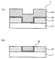
本発明の表面処理方法は、前記表面処理用組成物を半導体基板の金属配線を含む面に接触させ、半導体基板の金属配線を含む面を処理することを特徴としている。本発明の表面処理方法は、金属配線を含む面を有する半導体基板の処理に適用でき、シリコン等からなる基体上に、金属配線部を形成するための溝を有する絶縁膜と、この絶縁膜上にバリアメタル膜と、このバリアメタル膜上に金属配線材料が堆積された半導体基板の表面処理方法として好ましい。この半導体基板の断面図の一例を図1(b)に示す。図1(b)は図1(a)を化学機械研磨処理後の断面図であり、図1(a)に示した基板1は、たとえばシリコン製の基体11、絶縁膜12、バリアメタル膜13および配線部を形成する金属膜14からなる。
[2. Surface treatment method]
The surface treatment method of the present invention is characterized in that the surface treatment composition is brought into contact with a surface of a semiconductor substrate containing metal wiring, and the surface of the semiconductor substrate containing metal wiring is treated. The surface treatment method of the present invention can be applied to the processing of a semiconductor substrate having a surface including a metal wiring, and an insulating film having a groove for forming a metal wiring portion on a base made of silicon or the like, and the insulating film on the insulating film It is preferable as a surface treatment method for a semiconductor substrate having a barrier metal film and a metal wiring material deposited on the barrier metal film. An example of a cross-sectional view of this semiconductor substrate is shown in FIG. FIG. 1B is a cross-sectional view after chemical mechanical polishing of FIG. 1A. The substrate 1 shown in FIG. 1A includes a
本発明の表面処理方法を実施できる処理対象物は、半導体基板の、銅などの金属配線を含む面である。このような半導体基板の金属配線を含む面に存在する配線金属と絶縁膜あるいはバリアメタル膜との界面は、一般に容易に浸食されて楔状の欠陥(ファング)を発生させやすいが、本発明の表面処理用組成物を用いた表面処理方法を実施することにより、ファングの発生を抑制することができ、良好な状態の面を維持することができる。 An object to be processed on which the surface treatment method of the present invention can be performed is a surface of a semiconductor substrate including a metal wiring such as copper. In general, the interface between the wiring metal and the insulating film or the barrier metal film existing on the surface including the metal wiring of the semiconductor substrate is easily eroded to easily generate wedge-shaped defects (fangs). By performing the surface treatment method using the treatment composition, generation of fangs can be suppressed, and a good surface can be maintained.
本発明の表面処理方法は、前記表面処理用組成物を半導体基板の金属配線を含む面に接触させることができればよく、該接触させる方法は特に制限されない。
前記接触させる方法は、本発明の表面処理組成物を用いる点を除いて、定盤上処理、ブラシスクラブ処理およびロール処理などの従来公知の表面処理方法により実施することができる。また、スピンリンスドライ部などの回転中に表面処理用組成物を供給する、いわゆるスピンコート法にて処理することもできる。さらに表面処理後〜乾燥前の工程において表面処理用組成物を供給し、実施することもできる。
The surface treatment method of the present invention is not particularly limited as long as the composition for surface treatment can be brought into contact with the surface including the metal wiring of the semiconductor substrate.
The contact method can be carried out by a conventionally known surface treatment method such as surface plate treatment, brush scrub treatment and roll treatment, except that the surface treatment composition of the present invention is used. Moreover, it can also process by what is called a spin coat method which supplies the composition for surface treatment during rotation of a spin rinse dry part. Furthermore, the composition for surface treatment can also be supplied and implemented in the process after surface treatment-before drying.
定盤上処理による表面処理方法とは、例えば、定盤(例えば、研磨パッド)上でスラリー(化学機械研磨用水系分散体)の供給が終了した後、表面処理用組成物、必要に応じてイオン交換水(以下「DIW」とも記す。)を供給し、定盤および基板を回転させながら基板表面を処理する方法である。 The surface treatment method by surface plate treatment is, for example, a composition for surface treatment, if necessary, after the supply of slurry (chemical mechanical polishing aqueous dispersion) is completed on a surface plate (eg, polishing pad). In this method, ion exchange water (hereinafter also referred to as “DIW”) is supplied, and the surface of the substrate is treated while rotating the surface plate and the substrate.
ブラシスクラブ処理およびロール処理による表面処理方法とは、例えば、柔らかい素材(ポリビニルアルコール(PVA)など)でできたスポンジブラシを基板両面で回転させ、同時に基板を水平方向に回転させながら、イオン交換水(以下「DIW」とも記す。)や表面処理用組成物を供給し、基板表面を処理する方法である。 The surface treatment method by brush scrub treatment and roll treatment is, for example, ion-exchanged water while rotating a sponge brush made of a soft material (polyvinyl alcohol (PVA) etc.) on both sides of the substrate and simultaneously rotating the substrate in the horizontal direction. (Hereinafter also referred to as “DIW”) and a method of supplying a surface treatment composition to treat the substrate surface.
スピンコート法による処理方法とは、例えば、スピンリンスドライ部において回転させながら、DIWリンスを供給する前に、表面処理用組成物を供給し、基板表面を処理する方法である。 The treatment method by the spin coating method is, for example, a method of treating a substrate surface by supplying a composition for surface treatment before supplying DIW rinse while rotating in a spin rinse dry part.
本発明の表面処理方法によれば、半導体基板の金属配線の酸化を抑制でき、さらに半導体基板の金属配線を含む面に絶縁膜あるいはバリアメタル膜が存在する場合に、金属配線と絶縁膜あるいはバリアメタル膜との界面において発生するファングおよび金属配線の表面荒れを抑制できる。 According to the surface treatment method of the present invention, the oxidation of the metal wiring of the semiconductor substrate can be suppressed, and when the insulating film or the barrier metal film exists on the surface of the semiconductor substrate including the metal wiring, the metal wiring and the insulating film or barrier It is possible to suppress the surface roughness of the fang and metal wiring generated at the interface with the metal film.
[3.半導体装置の製造方法]
本発明の半導体装置の製造方法は、前記表面処理方法により半導体基板の金属配線を含む面を処理する工程を含んでいる。その他の工程は、従来公知の工程を用いることができる。
[3. Manufacturing method of semiconductor device]
The method for manufacturing a semiconductor device of the present invention includes a step of processing a surface including a metal wiring of a semiconductor substrate by the surface treatment method. Conventionally known processes can be used for the other processes.
前記表面処理方法により半導体基板の金属配線を含む面を処理する工程は、半導体基板を化学機械研磨した後に実施することが好ましい。前記表面処理方法により処理する工程は、たとえば、半導体基板を化学機械研磨した後、定盤上処理、ブラシスクラブ処理およびロール処理などの従来公知の表面処理により実施してもよく、スピンコートにより表面処理を実施してもよく、前記従来公知の表面処理後から乾燥工程前に実施してもよく、もしくは乾燥工程後に実施してもよい。 The step of treating the surface of the semiconductor substrate including the metal wiring by the surface treatment method is preferably performed after chemical mechanical polishing of the semiconductor substrate. The step of treating by the surface treatment method may be performed by a conventionally known surface treatment such as a surface plate treatment, a brush scrub treatment, and a roll treatment after chemical mechanical polishing of the semiconductor substrate. The treatment may be performed, may be performed after the conventionally known surface treatment and before the drying step, or may be performed after the drying step.
前記表面処理方法により半導体基板の金属配線を含む面を処理する工程を行うことにより、半導体基板の金属配線の酸化を抑制でき、次工程での還元プロセスが大幅に簡便化できる。したがって、本発明の半導体装置の製造方法によれば、費用を抑えて半導体装置を製造することができる。 By performing the process of processing the surface including the metal wiring of the semiconductor substrate by the surface treatment method, oxidation of the metal wiring of the semiconductor substrate can be suppressed, and the reduction process in the next process can be greatly simplified. Therefore, according to the method for manufacturing a semiconductor device of the present invention, it is possible to manufacture a semiconductor device at a reduced cost.
また、本発明の半導体装置の製造方法によれば、異常酸化による金属配線部の平坦性の悪化を抑制することができる。さらに半導体基板の金属配線を含む面に絶縁膜あるいはバリアメタル膜が存在する場合に、金属配線と絶縁膜あるいはバリアメタル膜との界面において発生するファングおよび金属配線の表面荒れを抑制できる。したがって、本発明の半導体装置の製造方法により得られる半導体装置は電気特性に優れる。 Moreover, according to the method for manufacturing a semiconductor device of the present invention, it is possible to suppress the deterioration of the flatness of the metal wiring portion due to abnormal oxidation. Furthermore, when an insulating film or a barrier metal film is present on the surface including the metal wiring of the semiconductor substrate, it is possible to suppress the surface roughness of the fang and the metal wiring generated at the interface between the metal wiring and the insulating film or the barrier metal film. Therefore, the semiconductor device obtained by the method for manufacturing a semiconductor device of the present invention is excellent in electrical characteristics.
以下、本発明について、実施例を挙げて具体的に説明するが、本発明はこれらの実施例に何ら限定されない。 EXAMPLES Hereinafter, although an Example is given and this invention is demonstrated concretely, this invention is not limited to these Examples at all.
[有機樹脂粒子含有水分散体の調製]
単量体としてメタクリル酸8質量部、ジビニルベンゼン20質量部およびスチレン72質量部と、重合開始剤として過硫酸アンモニウム0.5質量部と、界面活性剤としてドデシルベンゼンスルホン酸ナトリウム9質量部と、溶媒としてイオン交換水400質量部とをフラスコに入れ、窒素雰囲気下で攪拌しながら70℃に昇温し、さらに同温度で8時間攪拌して重合を行った。これにより、カルボキシル基および架橋構造を有し、平均分散粒径が50nmである有機樹脂粒子(以下「有機樹脂粒子c1」とも記す。)を含有する水分散体を得た。この水分散体にイオン交換水を加えて、有機樹脂粒子の含有割合が17質量%の有機樹脂粒子含有水分散体(CW)を調製した。
[Preparation of organic resin particle-containing aqueous dispersion]
8 parts by mass of methacrylic acid as a monomer, 20 parts by mass of divinylbenzene and 72 parts by mass of styrene, 0.5 part by mass of ammonium persulfate as a polymerization initiator, 9 parts by mass of sodium dodecylbenzenesulfonate as a surfactant, and a solvent As described above, 400 parts by mass of ion-exchanged water was placed in a flask, heated to 70 ° C. with stirring in a nitrogen atmosphere, and further stirred for 8 hours at the same temperature for polymerization. Thereby, an aqueous dispersion containing organic resin particles (hereinafter also referred to as “organic resin particles c1”) having a carboxyl group and a crosslinked structure and having an average dispersed particle diameter of 50 nm was obtained. Ion exchange water was added to this aqueous dispersion to prepare an organic resin particle-containing aqueous dispersion (CW) having a content of organic resin particles of 17% by mass.
[実施例1]
(i)表面処理用組成物の調製
ポリエチレン製容器に、化合物(A)として2−ピリジンカルボキシアルデヒド0.1質量部、表面活性剤としてクエン酸0.1質量部、水溶性(共)重合体(塩)としてポリアクリル酸0.1質量部、界面活性剤としてドデシルベンゼンスルホン酸0.007質量部を投入し、さらに、有機樹脂粒子c1が0.01質量部となるように、上記で調製した有機樹脂粒子含有水分散体(CW)を投入した。次に、全構成成分の合計量が100質量部となるように、溶媒(B)としてイオン交換水を加え、15分間攪拌した。次にpH調整剤としてテトラメチルアンモニウムヒドロキシド(以下「TMAH」とも記す。)を用いて、前記混合物のpHを調整した。その後、孔径5μmのフィルタで濾過して、pH4.5の表面処理用組成物(1)を得た。なお、表面処理組成物のpHは、(株)堀場製作所製のpHメーター「F52」を用いて測定した。当該測定結果を表1に示す。
[Example 1]
(I) Preparation of surface treatment composition In a polyethylene container, 0.1 part by mass of 2-pyridinecarboxaldehyde as a compound (A), 0.1 part by mass of citric acid as a surfactant, a water-soluble (co) polymer (Salt) 0.1 parts by weight of polyacrylic acid, 0.007 parts by weight of dodecylbenzenesulfonic acid as the surfactant are added, and further prepared so that the organic resin particles c1 are 0.01 parts by weight. The organic resin particle-containing aqueous dispersion (CW) was added. Next, ion-exchanged water was added as a solvent (B) so that the total amount of all the components was 100 parts by mass, and the mixture was stirred for 15 minutes. Next, the pH of the mixture was adjusted using tetramethylammonium hydroxide (hereinafter also referred to as “TMAH”) as a pH adjuster. Then, it filtered with the filter of the hole diameter of 5 micrometers, and obtained the composition (1) for surface treatment of pH4.5. The pH of the surface treatment composition was measured using a pH meter “F52” manufactured by Horiba, Ltd. The measurement results are shown in Table 1.
(ii)銅配線のパターン付き基板の化学機械研磨
銅配線のパターン付き基板(International SEMATECH製、シリコン基板上にPETEOS膜を厚さ5000Å積層させた後、「SEMATECH 854」マスクにてパターン加工し、その上に厚さ250ÅのTiN膜、1,000Åの銅シード膜および厚さ10,000Åの銅メッキ膜を順次積層させたテスト用の基板)(以下「SEMATECH 854」とも記す。)を、化学機械研磨装置「EPO112」((株)荏原製作所製)を用いて、下記の条件で二段階化学機械研磨した。
(Ii) Chemical mechanical polishing of a substrate with a copper wiring pattern A substrate with a copper wiring pattern (made by International SEMATECH, a PETEOS film having a thickness of 5000 mm laminated on a silicon substrate, and then patterned with a “SEMATECH 854” mask, A test substrate in which a TiN film having a thickness of 250 mm, a copper seed film having a thickness of 1,000 mm, and a copper plating film having a thickness of 10,000 mm are sequentially laminated (hereinafter also referred to as “SEMATECH 854”) is chemically prepared. Using a mechanical polishing apparatus “EPO112” (manufactured by Ebara Corporation), two-stage chemical mechanical polishing was performed under the following conditions.
(第一段目の化学機械研磨)
化学機械研磨用水系分散体種:JSR(株)製、「CMS7501/CMS7552」
研磨パッド:ロデール・ニッタ(株)製、「IC1000/SUBA400」
定盤回転数:70rpm
ヘッド回転数:70rpm
ヘッド荷重:50g/cm2
研磨用水系分散体供給速度:200mL/分
研磨時間:150秒
(第二段目の化学機械研磨)
化学機械研磨用水系分散体種:JSR(株)製、「CMS8501/CMS8552」
研磨パッド:ロデール・ニッタ(株)製、「IC1000/SUBA400」
定盤回転数:70rpm
ヘッド回転数:70rpm
ヘッド荷重:250g/cm2
研磨用水系分散体供給速度:200mL/分
研磨時間:60秒
(1st stage chemical mechanical polishing)
Chemical mechanical polishing aqueous dispersion type: “CMS7501 / CMS7552” manufactured by JSR Corporation
Polishing pad: Rodel Nitta Co., Ltd., “IC1000 / SUBA400”
Plate rotation speed: 70rpm
Head rotation speed: 70rpm
Head load: 50 g / cm 2
Polishing aqueous dispersion supply rate: 200 mL / min Polishing time: 150 seconds (second stage chemical mechanical polishing)
Chemical mechanical polishing aqueous dispersion type: JSR Corporation, “CMS8501 / CMS8552”
Polishing pad: Rodel Nitta Co., Ltd., “IC1000 / SUBA400”
Plate rotation speed: 70rpm
Head rotation speed: 70rpm
Head load: 250 g / cm 2
Polishing aqueous dispersion supply rate: 200 mL / min Polishing time: 60 seconds
(iii)表面処理
前記(ii)の化学機械研磨に続いて、研磨後の基板の銅配線を含む面に前記(i)で調製した表面処理用組成物(1)を接触させた。詳細には、下記の条件で定盤上洗浄工程、ブラシスクラブ洗浄工程において、一般的な洗浄剤の代わりに前記表面処理用組成物(1)を供給し、該組成物を半導体基板の金属配線を含む面に接触させた。その後、スピンリンスドライ部で、下記の条件で、基板の銅配線を含む面にイオン交換水(以下「DIW」とも記す。)を供給し、表面処理を行った。
(Iii) Surface Treatment Following the chemical mechanical polishing in (ii), the surface treatment composition (1) prepared in (i) was brought into contact with the surface of the substrate after polishing that included the copper wiring. Specifically, the surface treatment composition (1) is supplied in place of a general cleaning agent in the cleaning process on the surface plate and the brush scrub cleaning process under the following conditions, and the composition is used as the metal wiring of the semiconductor substrate. The surface containing was brought into contact. Thereafter, in the spin rinse dry section, ion exchange water (hereinafter also referred to as “DIW”) was supplied to the surface including the copper wiring of the substrate under the following conditions to perform surface treatment.
(定盤上洗浄工程)
ヘッド回転数:70rpm
ヘッド荷重:100g/cm2
定盤回転数:70rpm
表面処理組成物供給速度:300mL/分
表面処理時間:30秒
(ブラシスクラブ洗浄工程)
上部ブラシ回転数:100rpm
下部ブラシ回転数:100rpm
基板回転数:100rpm
表面処理組成物供給量:300mL/分
表面処理時間:30秒
(スピンリンスドライ処理)
基板回転数:100rpm
表面処理組成物供給量:300mL/分
表面処理時間:60秒
(Washing process on the surface plate)
Head rotation speed: 70rpm
Head load: 100 g / cm 2
Plate rotation speed: 70rpm
Surface treatment composition supply rate: 300 mL / min Surface treatment time: 30 seconds (Brush scrub cleaning process)
Upper brush rotation speed: 100rpm
Lower brush rotation speed: 100rpm
Substrate rotation speed: 100 rpm
Surface treatment composition supply amount: 300 mL / min Surface treatment time: 30 seconds (spin rinse dry treatment)
Substrate rotation speed: 100 rpm
Surface treatment composition supply amount: 300 mL / min Surface treatment time: 60 seconds
(iv)基板表面の評価
前記(iii)の表面処理後の基板表面全体について、ケーエルエー・テンコール(株)製のウェハ表面異物検査装置「KLA2351」およびアプライドマテリアルズ(株)製の欠陥レビューSEM「SEMVision G3 FIB」を用いて、スクラッチ欠陥、微小異物欠陥、楔状の浸食欠陥(ファング)および表面荒れについて観察した。結果を表2に示す。
(Iv) Evaluation of Substrate Surface Regarding the entire substrate surface after the surface treatment of (iii) above, a wafer surface foreign matter inspection apparatus “KLA2351” manufactured by KLA Tencor Co., Ltd. and a defect review SEM “Applied Materials Co., Ltd.” SEMVision G3 FIB "was used to observe scratch defects, minute foreign matter defects, wedge-shaped erosion defects (fangs), and surface roughness. The results are shown in Table 2.
次工程への影響を考慮して、スクラッチ欠陥、微小異物欠陥、楔状の浸食欠陥(ファング)については、基板表面(直径:8インチ)全体において、100個未満の場合を良好とし、100個以上の場合を不良とした。表面荒れについては1箇所でも存在した場合は、不良とした。 Considering the influence on the next process, scratch defects, minute foreign matter defects, wedge-shaped erosion defects (fangs) are good when the number is less than 100 on the entire substrate surface (diameter: 8 inches), and 100 or more. The case of was considered defective. When the surface roughness was present even at one location, it was regarded as defective.
(v)異常酸化の確認
前記(iii)の表面処理後の基板を、温度40℃・湿度100%の高温高湿の状態で3日間静置した後、デジタルインスツルメンツ(現ビーコインスツルメンツ)製の原子間力顕微鏡「NanoScope IIIa」を用いて、銅配線(10μm×10μm)における異常酸化の有無を観察した。結果を表2に示す。銅配線に高さ10nm以上の凸状部位が1箇所でも存在した場合は、異常酸化有りとした。
(V) Confirmation of abnormal oxidation The substrate after the surface treatment of (iii) is left in a high-temperature and high-humidity state at a temperature of 40 ° C. and a humidity of 100% for 3 days, and then an atom made by Digital Instruments (currently Becoins Instruments). Using an atomic force microscope “NanoScope IIIa”, the presence or absence of abnormal oxidation in the copper wiring (10 μm × 10 μm) was observed. The results are shown in Table 2. When even one convex portion with a height of 10 nm or more exists in the copper wiring, it is considered that there is abnormal oxidation.
(vi)酸化銅膜厚測定
配線のパターンの無い銅薄膜付基板(ATDF社製、8inch Cuメッキ15,000Å)を、前記(i)で調製した表面処理用組成物(1)に60秒間浸漬し、30秒間水洗することにより、基板表面処理を行った。表面処理後の酸化銅膜厚を、北斗電工(株)製の電気化学測定システムHZ−3000を用いたCV法で測定した。結果を表2に示す。
(Vi) Measurement of copper oxide film thickness A substrate with a copper thin film without a wiring pattern (ATDF, 8 inch Cu plating 15,000 mm) was immersed in the surface treatment composition (1) prepared in (i) for 60 seconds. Then, the substrate surface treatment was performed by washing with water for 30 seconds. The copper oxide film thickness after the surface treatment was measured by a CV method using an electrochemical measurement system HZ-3000 manufactured by Hokuto Denko Corporation. The results are shown in Table 2.
待機中や測定中などに自然に形成される酸化銅の膜厚を諸所の文献等から20〜30Åと想定し、表面処理後の酸化銅膜厚が30Å以下の場合を良好とし、30Åを超えた場合を表面処理後の次工程での還元プロセスへの影響を考え、不良とした。 Assuming that the film thickness of copper oxide naturally formed during standby or measurement is 20 to 30 mm from various literatures, etc., the case where the copper oxide film thickness after surface treatment is 30 mm or less is considered good, In the case of exceeding, the influence on the reduction process in the next step after the surface treatment was considered and it was determined as defective.
[実施例2]
(i)表面処理用組成物の調製
表面活性剤としてマレイン酸を用い、pH調整剤(TMAH)によりpHを6.2に調整した以外は、実施例1と同様にして表面処理用組成物(2)を得た。
[Example 2]
(I) Preparation of surface treatment composition Surface treatment composition (same as in Example 1) except that maleic acid was used as the surface active agent and the pH was adjusted to 6.2 with a pH adjuster (TMAH). 2) was obtained.
(ii)銅配線のパターン付き基板の化学機械研磨
実施例1と同様にして銅配線のパターン付き基板「SEMATECH 854」を、化学機械研磨装置「EPO112」((株)荏原製作所製)を用いて二段階化学機械研磨した。
(Ii) Chemical mechanical polishing of copper wiring pattern substrate Substrate “SEMATECH 854” with copper wiring pattern was used in the same manner as in Example 1 using chemical mechanical polishing device “EPO112” (manufactured by Ebara Corporation). Two-stage chemical mechanical polishing.
(iii)表面処理および評価
表面処理用組成物(1)の代わりに表面処理用組成物(2)を用いた以外は実施例1と同様にして表面処理を行い、基板表面の評価、異常酸化の確認、酸化銅膜厚測定を行った。結果を表2に示す。
(Iii) Surface treatment and evaluation Surface treatment is performed in the same manner as in Example 1 except that the surface treatment composition (2) is used instead of the surface treatment composition (1), and the substrate surface is evaluated and abnormally oxidized. And copper oxide film thickness was measured. The results are shown in Table 2.
[実施例3]
(i)表面処理用組成物の調製
表面活性剤としてマレイン酸を用い、pH調整剤(TMAH)によりpHを10.0に調整した以外は、実施例1と同様にして表面処理用組成物(3)を得た。
[Example 3]
(I) Preparation of surface treatment composition Surface treatment composition (same as in Example 1) except that maleic acid was used as the surface active agent and the pH was adjusted to 10.0 with a pH adjuster (TMAH). 3) was obtained.
(ii)銅配線のパターン付き基板の化学機械研磨
実施例1と同様にして銅配線のパターン付き基板「SEMATECH 854」を、化学機械研磨装置「EPO112」((株)荏原製作所製)を用いて二段階化学機械研磨した。
(Ii) Chemical mechanical polishing of copper wiring pattern substrate Substrate “SEMATECH 854” with copper wiring pattern was used in the same manner as in Example 1 using chemical mechanical polishing device “EPO112” (manufactured by Ebara Corporation). Two-stage chemical mechanical polishing.
(iii)表面処理および評価
表面処理用組成物(1)の代わりに表面処理用組成物(3)を用いた以外は実施例1と同様にして表面処理を行い、基板表面の評価、異常酸化の確認、酸化銅膜厚測定を行った。結果を表2に示す。
(Iii) Surface treatment and evaluation Surface treatment was performed in the same manner as in Example 1 except that the surface treatment composition (3) was used instead of the surface treatment composition (1), and the substrate surface was evaluated and abnormally oxidized. And copper oxide film thickness was measured. The results are shown in Table 2.
[実施例4]
(i)表面処理用組成物の調製
表面活性剤、水溶性(共)重合体(塩)および界面活性剤を用いず、化合物(A)の配合量を0.3質量部とし、pH調整剤(TMAH)によりpHを6.2に調整した以外は、実施例1と同様にして表面処理用組成物(4)を得た。
[Example 4]
(I) Preparation of surface treatment composition A surfactant, a water-soluble (co) polymer (salt) and a surfactant are not used, the compounding amount of compound (A) is 0.3 parts by mass, and a pH adjuster A surface treatment composition (4) was obtained in the same manner as in Example 1 except that the pH was adjusted to 6.2 with (TMAH).
(ii)銅配線のパターン付き基板の化学機械研磨
実施例1と同様にして銅配線のパターン付き基板「SEMATECH 854」を、化学機械研磨装置「EPO112」((株)荏原製作所製)を用いて二段階化学機械研磨した。
(Ii) Chemical mechanical polishing of copper wiring pattern substrate Substrate “SEMATECH 854” with copper wiring pattern was used in the same manner as in Example 1 using chemical mechanical polishing device “EPO112” (manufactured by Ebara Corporation). Two-stage chemical mechanical polishing.
(iii)表面処理および評価
表面処理用組成物(1)の代わりに表面処理用組成物(4)を用いた以外は実施例1と同様にして表面処理を行い、基板表面の評価、異常酸化の確認、酸化銅膜厚測定を行った。結果を表2に示す。
(Iii) Surface treatment and evaluation Surface treatment was performed in the same manner as in Example 1 except that the surface treatment composition (4) was used instead of the surface treatment composition (1), and the substrate surface was evaluated and abnormally oxidized. And copper oxide film thickness was measured. The results are shown in Table 2.
[実施例5]
(i)表面処理用組成物の調製
表面活性剤、水溶性(共)重合体(塩)、有機樹脂粒子、界面活性剤およびpH調整剤を用いず、化合物(A)の配合量を0.3質量部とした以外は、実施例1と同様にしてpH6.2の表面処理用組成物(5)を得た。
[Example 5]
(I) Preparation of composition for surface treatment The amount of compound (A) is adjusted to 0, without using a surfactant, a water-soluble (co) polymer (salt), organic resin particles, a surfactant and a pH adjuster. A surface treatment composition (5) having a pH of 6.2 was obtained in the same manner as in Example 1 except that the amount was 3 parts by mass.
(ii)銅配線のパターン付き基板の化学機械研磨
実施例1と同様にして銅配線のパターン付き基板「SEMATECH 854」を、化学機械研磨装置「EPO112」((株)荏原製作所製)を用いて二段階化学機械研磨した。
(Ii) Chemical mechanical polishing of copper wiring pattern substrate Substrate “SEMATECH 854” with copper wiring pattern was used in the same manner as in Example 1 using chemical mechanical polishing device “EPO112” (manufactured by Ebara Corporation). Two-stage chemical mechanical polishing.
(iii)表面処理および評価
表面処理用組成物(1)の代わりに表面処理用組成物(5)を用いた以外は実施例1と同様にして表面処理を行い、基板表面の評価、異常酸化の確認、酸化銅膜厚測定を行った。結果を表2に示す。
(Iii) Surface treatment and evaluation Surface treatment was performed in the same manner as in Example 1 except that the surface treatment composition (5) was used instead of the surface treatment composition (1), and the substrate surface was evaluated and abnormally oxidized. And copper oxide film thickness was measured. The results are shown in Table 2.
[比較例1]
(i)表面処理用組成物の調製
pH調整剤(TMAH)によりpHを3.0に調整した以外は、実施例1と同様にして表面処理用組成物(6)を得た。
[Comparative Example 1]
(I) Preparation of surface treatment composition A surface treatment composition (6) was obtained in the same manner as in Example 1 except that the pH was adjusted to 3.0 with a pH adjuster (TMAH).
(ii)銅配線のパターン付き基板の化学機械研磨
実施例1と同様にして銅配線のパターン付き基板「SEMATECH 854」を、化学機械研磨装置「EPO112」((株)荏原製作所製)を用いて二段階化学機械研磨した。
(Ii) Chemical mechanical polishing of copper wiring pattern substrate Substrate “SEMATECH 854” with copper wiring pattern was used in the same manner as in Example 1 using chemical mechanical polishing device “EPO112” (manufactured by Ebara Corporation). Two-stage chemical mechanical polishing.
(iii)表面処理および評価
表面処理用組成物(1)の代わりに表面処理用組成物(6)を用いた以外は実施例1と同様にして表面処理を行い、基板表面の評価、異常酸化の確認、酸化銅膜厚測定を行った。結果を表3に示す。
(Iii) Surface treatment and evaluation Surface treatment was performed in the same manner as in Example 1 except that the surface treatment composition (6) was used instead of the surface treatment composition (1), and the substrate surface was evaluated and abnormally oxidized. And copper oxide film thickness was measured. The results are shown in Table 3.
[比較例2]
(i)表面処理用組成物の調製
pH調整剤(TMAH)によりpHを12.0に調整した以外は、実施例1と同様にして表面処理用組成物(7)を得た。
[Comparative Example 2]
(I) Preparation of surface treatment composition A surface treatment composition (7) was obtained in the same manner as in Example 1 except that the pH was adjusted to 12.0 with a pH adjuster (TMAH).
(ii)銅配線のパターン付き基板の化学機械研磨
実施例1と同様にして銅配線のパターン付き基板「SEMATECH 854」を、化学機械研磨装置「EPO112」((株)荏原製作所製)を用いて二段階化学機械研磨した。
(Ii) Chemical mechanical polishing of copper wiring pattern substrate Substrate “SEMATECH 854” with copper wiring pattern was used in the same manner as in Example 1 using chemical mechanical polishing device “EPO112” (manufactured by Ebara Corporation). Two-stage chemical mechanical polishing.
(iii)表面処理および評価
表面処理用組成物(1)の代わりに表面処理用組成物(7)を用いた以外は実施例1と同様にして表面処理を行い、基板表面の評価、異常酸化の確認、酸化銅膜厚測定を行った。結果を表3に示す。
(Iii) Surface treatment and evaluation Surface treatment is performed in the same manner as in Example 1 except that the surface treatment composition (7) is used instead of the surface treatment composition (1), and the substrate surface is evaluated and abnormally oxidized. And copper oxide film thickness was measured. The results are shown in Table 3.
[比較例3]
(i)表面処理用組成物の調製
化合物(A)を用いなかった以外は、実施例1と同様にして表面処理用組成物(8)を得た。
[Comparative Example 3]
(I) Preparation of surface treatment composition A surface treatment composition (8) was obtained in the same manner as in Example 1 except that the compound (A) was not used.
(ii)銅配線のパターン付き基板の化学機械研磨
実施例1と同様にして銅配線のパターン付き基板「SEMATECH 854」を、化学機械研磨装置「EPO112」((株)荏原製作所製)を用いて二段階化学機械研磨した。
(Ii) Chemical mechanical polishing of copper wiring pattern substrate Substrate “SEMATECH 854” with copper wiring pattern was used in the same manner as in Example 1 using chemical mechanical polishing device “EPO112” (manufactured by Ebara Corporation). Two-stage chemical mechanical polishing.
(iii)表面処理および評価
表面処理用組成物(1)の代わりに表面処理用組成物(8)を用いた以外は実施例1と同様にして表面処理を行い、基板表面の評価、異常酸化の確認、酸化銅膜厚測定を行った。結果を表3に示す。銅配線の異常酸化は9箇所であった。
(Iii) Surface treatment and evaluation Surface treatment was performed in the same manner as in Example 1 except that the surface treatment composition (8) was used instead of the surface treatment composition (1), and the substrate surface was evaluated and abnormally oxidized. And copper oxide film thickness was measured. The results are shown in Table 3. There were 9 abnormal oxidations of the copper wiring.
[比較例4]
(i)表面処理用組成物の調製
化合物(A)を用いなかった以外は、実施例2と同様にして表面処理用組成物(9)を得た。
[Comparative Example 4]
(I) Preparation of surface treatment composition A surface treatment composition (9) was obtained in the same manner as in Example 2 except that the compound (A) was not used.
(ii)銅配線のパターン付き基板の化学機械研磨
実施例1と同様にして銅配線のパターン付き基板「SEMATECH 854」を、化学機械研磨装置「EPO112」((株)荏原製作所製)を用いて二段階化学機械研磨した。
(Ii) Chemical mechanical polishing of copper wiring pattern substrate Substrate “SEMATECH 854” with copper wiring pattern was used in the same manner as in Example 1 using chemical mechanical polishing device “EPO112” (manufactured by Ebara Corporation). Two-stage chemical mechanical polishing.
(iii)表面処理および評価
表面処理用組成物(1)の代わりに表面処理用組成物(9)を用いた以外は実施例1と同様にして表面処理を行い、基板表面の評価、異常酸化の確認、酸化銅膜厚測定を行った。結果を表3に示す。銅配線の異常酸化は6箇所であった。
(Iii) Surface treatment and evaluation Surface treatment was performed in the same manner as in Example 1 except that the surface treatment composition (9) was used instead of the surface treatment composition (1), and the substrate surface was evaluated and abnormally oxidized. And copper oxide film thickness was measured. The results are shown in Table 3. There were 6 abnormal oxidations of the copper wiring.
[比較例5]
(i)表面処理用組成物の調製
化合物(A)を用いなかった以外は、実施例3と同様にして表面処理用組成物(10)を得た。
[Comparative Example 5]
(I) Preparation of surface treatment composition A surface treatment composition (10) was obtained in the same manner as in Example 3 except that the compound (A) was not used.
(ii)銅配線のパターン付き基板の化学機械研磨
実施例1と同様にして銅配線のパターン付き基板「SEMATECH 854」を、化学機械研磨装置「EPO112」((株)荏原製作所製)を用いて二段階化学機械研磨した。
(Ii) Chemical mechanical polishing of copper wiring pattern substrate Substrate “SEMATECH 854” with copper wiring pattern was used in the same manner as in Example 1 using chemical mechanical polishing device “EPO112” (manufactured by Ebara Corporation). Two-stage chemical mechanical polishing.
(iii)表面処理および評価
表面処理用組成物(1)の代わりに表面処理用組成物(10)を用いた以外は実施例1と同様にして表面処理を行い、基板表面の評価、異常酸化の確認、酸化銅膜厚測定を行った。結果を表3に示す。銅配線の異常酸化は3箇所であった。
(Iii) Surface treatment and evaluation Surface treatment was performed in the same manner as in Example 1 except that the surface treatment composition (10) was used instead of the surface treatment composition (1), and the substrate surface was evaluated and abnormally oxidized. And copper oxide film thickness was measured. The results are shown in Table 3. There were three abnormal oxidations of the copper wiring.
[実施例6]
表面処理用組成物(1)の代わりに表面処理用組成物(8)を用い、DIWの代わりに表面処理用組成物(5)を用いた以外は実施例1と同様にして表面処理を行い、基板表面の評価、異常酸化の確認、酸化銅膜厚測定を行った。結果を表2に示す。
[Example 6]
Surface treatment was performed in the same manner as in Example 1 except that the surface treatment composition (8) was used instead of the surface treatment composition (1) and the surface treatment composition (5) was used instead of DIW. The substrate surface was evaluated, abnormal oxidation was confirmed, and the copper oxide film thickness was measured. The results are shown in Table 2.
[実施例7]
表面処理用組成物(1)の代わりに表面処理用組成物(9)を用い、DIWの代わりに表面処理用組成物(5)を用いた以外は実施例1と同様にして表面処理を行い、基板表面の評価、異常酸化の確認、酸化銅膜厚測定を行った。結果を表2に示す。
[Example 7]
Surface treatment was performed in the same manner as in Example 1 except that the surface treatment composition (9) was used instead of the surface treatment composition (1) and the surface treatment composition (5) was used instead of DIW. The substrate surface was evaluated, abnormal oxidation was confirmed, and the copper oxide film thickness was measured. The results are shown in Table 2.
[実施例8]
表面処理用組成物(1)の代わりに表面処理用組成物(10)を用い、DIWの代わりに表面処理用組成物(5)を用いた以外は実施例1と同様にして表面処理を行い、基板表面の評価、異常酸化の確認、酸化銅膜厚測定を行った。結果を表2に示す。
[Example 8]
Surface treatment was performed in the same manner as in Example 1 except that the surface treatment composition (10) was used instead of the surface treatment composition (1) and the surface treatment composition (5) was used instead of DIW. The substrate surface was evaluated, abnormal oxidation was confirmed, and the copper oxide film thickness was measured. The results are shown in Table 2.
[比較例6]
(i)表面処理用組成物の調製
表面活性剤、水溶性(共)重合体(塩)、有機樹脂粒子および界面活性剤を用いず、化合物(A)の配合量を0.3質量部とし、pH調整剤(リン酸)によりpHを3.0に調整した以外は、実施例1と同様にして表面処理用組成物(11)を得た。
[Comparative Example 6]
(I) Preparation of surface treatment composition Without using a surfactant, a water-soluble (co) polymer (salt), organic resin particles and a surfactant, the amount of compound (A) is 0.3 parts by mass. A surface treatment composition (11) was obtained in the same manner as in Example 1 except that the pH was adjusted to 3.0 with a pH adjuster (phosphoric acid).
(ii)表面処理および評価
表面処理用組成物(1)の代わりに表面処理用組成物(9)を用い、DIWの代わりに表面処理用組成物(11)を用いた以外は実施例1と同様にして表面処理を行い、基板表面の評価、異常酸化の確認、酸化銅膜厚測定を行った。結果を表3に示す。銅配線の異常酸化は2箇所であった。
(Ii) Surface treatment and evaluation Example 1 except that the surface treatment composition (9) was used instead of the surface treatment composition (1) and the surface treatment composition (11) was used instead of DIW. Surface treatment was performed in the same manner, and evaluation of the substrate surface, confirmation of abnormal oxidation, and measurement of the copper oxide film thickness were performed. The results are shown in Table 3. There were two abnormal oxidations of the copper wiring.
[比較例7]
(i)表面処理用組成物の調製
表面活性剤、水溶性(共)重合体(塩)、有機樹脂粒子および界面活性剤を用いず、化合物(A)の配合量を0.3質量部とし、pH調整剤(TMAH)によりpHを12.0に調整した以外は、実施例1と同様にして表面処理用組成物(12)を得た。
[Comparative Example 7]
(I) Preparation of surface treatment composition Without using a surfactant, a water-soluble (co) polymer (salt), organic resin particles and a surfactant, the amount of compound (A) is 0.3 parts by mass. A surface treatment composition (12) was obtained in the same manner as in Example 1 except that the pH was adjusted to 12.0 with a pH adjuster (TMAH).
(ii)表面処理および評価
表面処理用組成物(1)の代わりに表面処理用組成物(9)を用い、DIWの代わりに表面処理用組成物(12)を用いた以外は実施例1と同様にして表面処理を行い、基板表面の評価、異常酸化の確認、酸化銅膜厚測定を行った。結果を表3に示す。
(Ii) Surface treatment and evaluation Example 1 except that the surface treatment composition (9) was used instead of the surface treatment composition (1) and the surface treatment composition (12) was used instead of DIW. Surface treatment was performed in the same manner, and evaluation of the substrate surface, confirmation of abnormal oxidation, and measurement of the copper oxide film thickness were performed. The results are shown in Table 3.
1 半導体基板素材
11 基体(例えば、シリコン製)
12 絶縁膜(例えば、PETEOS製)
13 バリアメタル膜
14 金属膜
1
12 Insulating film (for example, made by PETEOS)
13
Claims (5)
1気圧下における沸点が50〜300℃である溶媒(B)とを含み、
pHが4〜11である、
半導体基板の、金属配線を含む面を処理するための表面処理用組成物。
A solvent (B) having a boiling point of 50 to 300 ° C. under 1 atm,
pH is 4-11,
A composition for surface treatment for treating a surface of a semiconductor substrate containing metal wiring.
Priority Applications (6)
| Application Number | Priority Date | Filing Date | Title |
|---|---|---|---|
| JP2009136098A JP5455452B2 (en) | 2009-06-05 | 2009-06-05 | Composition for surface treatment, method for surface treatment, and method for producing semiconductor device |
| KR1020117029025A KR20120036822A (en) | 2009-06-05 | 2010-06-01 | Surface treatment composition, surface treatment method, and method for manufacturing semiconductor device |
| PCT/JP2010/059277 WO2010140592A1 (en) | 2009-06-05 | 2010-06-01 | Surface treatment composition, surface treatment method, and method for manufacturing semiconductor device |
| EP10783375.8A EP2439767A4 (en) | 2009-06-05 | 2010-06-01 | Surface treatment composition, surface treatment method, and method for manufacturing semiconductor device |
| US12/794,028 US8257504B2 (en) | 2009-06-05 | 2010-06-04 | Surface treatment composition, surface treatment method, and method for manufacturing semiconductor device |
| TW099118156A TWI553117B (en) | 2009-06-05 | 2010-06-04 | Surface treatment composition, surface treatment method, and method for manufacturing semiconductor device |
Applications Claiming Priority (1)
| Application Number | Priority Date | Filing Date | Title |
|---|---|---|---|
| JP2009136098A JP5455452B2 (en) | 2009-06-05 | 2009-06-05 | Composition for surface treatment, method for surface treatment, and method for producing semiconductor device |
Publications (2)
| Publication Number | Publication Date |
|---|---|
| JP2010283198A JP2010283198A (en) | 2010-12-16 |
| JP5455452B2 true JP5455452B2 (en) | 2014-03-26 |
Family
ID=43297726
Family Applications (1)
| Application Number | Title | Priority Date | Filing Date |
|---|---|---|---|
| JP2009136098A Active JP5455452B2 (en) | 2009-06-05 | 2009-06-05 | Composition for surface treatment, method for surface treatment, and method for producing semiconductor device |
Country Status (6)
| Country | Link |
|---|---|
| US (1) | US8257504B2 (en) |
| EP (1) | EP2439767A4 (en) |
| JP (1) | JP5455452B2 (en) |
| KR (1) | KR20120036822A (en) |
| TW (1) | TWI553117B (en) |
| WO (1) | WO2010140592A1 (en) |
Families Citing this family (5)
| Publication number | Priority date | Publication date | Assignee | Title |
|---|---|---|---|---|
| JP6014985B2 (en) * | 2010-10-01 | 2016-10-26 | 三菱化学株式会社 | Substrate cleaning solution for semiconductor device and cleaning method |
| EP3112436A4 (en) | 2014-02-26 | 2017-02-22 | Fujimi Incorporated | Polishing composition |
| TWI636131B (en) * | 2014-05-20 | 2018-09-21 | 日商Jsr股份有限公司 | Cleaning composition and cleaning method |
| US10319605B2 (en) | 2016-05-10 | 2019-06-11 | Jsr Corporation | Semiconductor treatment composition and treatment method |
| JP6857996B2 (en) * | 2016-10-25 | 2021-04-14 | 日本パーカライジング株式会社 | Surface treatment agent, film and surface treatment method |
Family Cites Families (8)
| Publication number | Priority date | Publication date | Assignee | Title |
|---|---|---|---|---|
| US7097541B2 (en) * | 2002-01-22 | 2006-08-29 | Cabot Microelectronics Corporation | CMP method for noble metals |
| US7316603B2 (en) * | 2002-01-22 | 2008-01-08 | Cabot Microelectronics Corporation | Compositions and methods for tantalum CMP |
| US6527622B1 (en) | 2002-01-22 | 2003-03-04 | Cabot Microelectronics Corporation | CMP method for noble metals |
| JP2004123950A (en) * | 2002-10-04 | 2004-04-22 | Mitsui Chemicals Inc | Abrasive |
| JP2004335689A (en) * | 2003-05-07 | 2004-11-25 | Mitsui Chemicals Inc | Slurry for polishing copper |
| US7803203B2 (en) | 2005-09-26 | 2010-09-28 | Cabot Microelectronics Corporation | Compositions and methods for CMP of semiconductor materials |
| JPWO2007108215A1 (en) | 2006-03-20 | 2009-08-06 | 三井化学株式会社 | Polishing composition |
| JP2007291505A (en) | 2006-03-31 | 2007-11-08 | Sanyo Chem Ind Ltd | Detergent for copper wiring |
-
2009
- 2009-06-05 JP JP2009136098A patent/JP5455452B2/en active Active
-
2010
- 2010-06-01 WO PCT/JP2010/059277 patent/WO2010140592A1/en active Application Filing
- 2010-06-01 EP EP10783375.8A patent/EP2439767A4/en not_active Withdrawn
- 2010-06-01 KR KR1020117029025A patent/KR20120036822A/en not_active Application Discontinuation
- 2010-06-04 US US12/794,028 patent/US8257504B2/en active Active
- 2010-06-04 TW TW099118156A patent/TWI553117B/en active
Also Published As
| Publication number | Publication date |
|---|---|
| US8257504B2 (en) | 2012-09-04 |
| JP2010283198A (en) | 2010-12-16 |
| TW201105790A (en) | 2011-02-16 |
| US20100311630A1 (en) | 2010-12-09 |
| EP2439767A4 (en) | 2013-05-15 |
| WO2010140592A1 (en) | 2010-12-09 |
| EP2439767A1 (en) | 2012-04-11 |
| KR20120036822A (en) | 2012-04-18 |
| TWI553117B (en) | 2016-10-11 |
Similar Documents
| Publication | Publication Date | Title |
|---|---|---|
| EP1888735B1 (en) | Copper passivating post-chemical mechanical polishing cleaning composition and method of use | |
| KR100775199B1 (en) | Cleaning Composition, Method for Cleaning Semiconductor Substrate, and Process for Manufacturing Semiconductor Device | |
| JP4821122B2 (en) | Cleaning composition, semiconductor substrate cleaning method, and semiconductor device manufacturing method | |
| US20080045016A1 (en) | Cleaning composition, cleaning method, and manufacturing method of semiconductor device | |
| KR102314305B1 (en) | Cleaning composition and cleaning method | |
| US11149235B2 (en) | Cleaning composition with corrosion inhibitor | |
| TW200538544A (en) | Alkaline post-chemical mechanical planarization cleaning compositions | |
| JP2008004621A (en) | SLURRY FOR USE IN Cu FILM CMP, POLISHING METHOD, AND MANUFACTURING METHOD OF SEMICONDUCTOR DEVICE | |
| US10507563B2 (en) | Treatment composition for chemical mechanical polishing, chemical mechanical polishing method, and cleaning method | |
| JP6886469B2 (en) | Cleaning composition after chemical mechanical polishing | |
| JP5455452B2 (en) | Composition for surface treatment, method for surface treatment, and method for producing semiconductor device | |
| JP6949846B2 (en) | Cleaning composition after chemical mechanical polishing | |
| JP2010258014A (en) | Composition for cleaning, and cleaning method | |
| TW200823285A (en) | Rinse formulation for use in the manufacture of an integrated circuit | |
| JP2018092960A (en) | Cleaning composition and cleaning method | |
| WO2020255603A1 (en) | Polishing liquid and chemical-mechanical polishing method | |
| EP2687589A2 (en) | Copper passivating post-chemical mechanical polishing cleaning composition and method of use | |
| CN113774390B (en) | Cleaning liquid for chemical mechanical polishing and preparation method thereof | |
| JP7276343B2 (en) | Cleaning liquid, cleaning method, and semiconductor wafer manufacturing method | |
| WO2020255581A1 (en) | Polishing fluid and chemical mechanical polishing method | |
| WO2023096862A1 (en) | Microelectronic device cleaning composition |
Legal Events
| Date | Code | Title | Description |
|---|---|---|---|
| RD02 | Notification of acceptance of power of attorney |
Free format text: JAPANESE INTERMEDIATE CODE: A7422 Effective date: 20120305 |
|
| RD02 | Notification of acceptance of power of attorney |
Free format text: JAPANESE INTERMEDIATE CODE: A7422 Effective date: 20120323 |
|
| A621 | Written request for application examination |
Free format text: JAPANESE INTERMEDIATE CODE: A621 Effective date: 20120406 |
|
| A521 | Request for written amendment filed |
Free format text: JAPANESE INTERMEDIATE CODE: A821 Effective date: 20120323 |
|
| A131 | Notification of reasons for refusal |
Free format text: JAPANESE INTERMEDIATE CODE: A131 Effective date: 20130430 |
|
| A521 | Request for written amendment filed |
Free format text: JAPANESE INTERMEDIATE CODE: A523 Effective date: 20130627 |
|
| TRDD | Decision of grant or rejection written | ||
| A01 | Written decision to grant a patent or to grant a registration (utility model) |
Free format text: JAPANESE INTERMEDIATE CODE: A01 Effective date: 20131224 |
|
| A61 | First payment of annual fees (during grant procedure) |
Free format text: JAPANESE INTERMEDIATE CODE: A61 Effective date: 20140107 |
|
| R150 | Certificate of patent or registration of utility model |
Ref document number: 5455452 Country of ref document: JP Free format text: JAPANESE INTERMEDIATE CODE: R150 Free format text: JAPANESE INTERMEDIATE CODE: R150 |
|
| R250 | Receipt of annual fees |
Free format text: JAPANESE INTERMEDIATE CODE: R250 |
|
| S111 | Request for change of ownership or part of ownership |
Free format text: JAPANESE INTERMEDIATE CODE: R313115 |
|
| R350 | Written notification of registration of transfer |
Free format text: JAPANESE INTERMEDIATE CODE: R350 |
|
| R250 | Receipt of annual fees |
Free format text: JAPANESE INTERMEDIATE CODE: R250 |
|
| R250 | Receipt of annual fees |
Free format text: JAPANESE INTERMEDIATE CODE: R250 |
|
| R250 | Receipt of annual fees |
Free format text: JAPANESE INTERMEDIATE CODE: R250 |
|
| R250 | Receipt of annual fees |
Free format text: JAPANESE INTERMEDIATE CODE: R250 |
|
| R250 | Receipt of annual fees |
Free format text: JAPANESE INTERMEDIATE CODE: R250 |
|
| S111 | Request for change of ownership or part of ownership |
Free format text: JAPANESE INTERMEDIATE CODE: R313115 |
|
| R350 | Written notification of registration of transfer |
Free format text: JAPANESE INTERMEDIATE CODE: R350 |
|
| R250 | Receipt of annual fees |
Free format text: JAPANESE INTERMEDIATE CODE: R250 |