JP5445846B2 - Lighting device - Google Patents
Lighting device Download PDFInfo
- Publication number
- JP5445846B2 JP5445846B2 JP2010014706A JP2010014706A JP5445846B2 JP 5445846 B2 JP5445846 B2 JP 5445846B2 JP 2010014706 A JP2010014706 A JP 2010014706A JP 2010014706 A JP2010014706 A JP 2010014706A JP 5445846 B2 JP5445846 B2 JP 5445846B2
- Authority
- JP
- Japan
- Prior art keywords
- substrate
- radiator
- electric wire
- front surface
- light emitting
- Prior art date
- Legal status (The legal status is an assumption and is not a legal conclusion. Google has not performed a legal analysis and makes no representation as to the accuracy of the status listed.)
- Expired - Fee Related
Links
Images


Description
本発明は、光源として半導体発光素子を用いた照明装置に関する。 The present invention relates to a lighting device using a semiconductor light emitting element as a light source.
従来、例えば、展示物の照明に用いられるスポットライトなどの照明装置では、光源としてLEDを用いているものがある。 2. Description of the Related Art Conventionally, for example, some lighting devices such as spotlights used for illuminating exhibits have used LEDs as light sources.
このような照明装置では、複数のLEDを実装した基板、各LEDからの光を投光する複数のレンズ、これら基板およびレンズを収容する本体を備え、この本体がアームによって天井側から支持され、光を出射する本体の前面の向きをアームに対して回転方向および上下方向に調整可能としている。 In such an illuminating device, a substrate on which a plurality of LEDs are mounted, a plurality of lenses that project light from each LED, a substrate and a main body that accommodates the lens, and the main body is supported from the ceiling side by an arm, The direction of the front surface of the main body that emits light can be adjusted in the rotational direction and the vertical direction with respect to the arm.
本体は、基板が前面部に取り付けられる放熱体、および全体を覆うカバーなどを備え、外部からの電源供給用の電線が本体内に引き込まれて基板に電気的に接続されている(例えば、特許文献1参照。)。 The main body includes a heat radiating body to which the board is attached to the front surface, a cover that covers the whole, and the like, and an electric power supply wire from outside is drawn into the main body and electrically connected to the board (for example, a patent) Reference 1).
しかしながら、従来の照明器具では、半導体発光素子が発光時に発生する熱が、基板から放熱体に効率よく熱伝導されなかった。 However, in the conventional lighting fixture, the heat generated when the semiconductor light emitting element emits light is not efficiently conducted from the substrate to the heat radiator.
本発明は、このような点に鑑みなされたもので、半導体発光素子が発光時に発生する熱を、基板から放熱体に効率よく熱伝導できる照明装置を提供することを目的とする。 This invention is made | formed in view of such a point, and it aims at providing the illuminating device which can carry out the heat | fever which the semiconductor light-emitting element generate | occur | produces at the time of light emission efficiently from a board | substrate to a heat radiator.
請求項1記載の照明装置は、複数の半導体発光素子が少なくとも周辺部に実装されるとともに半導体発光素子が実装される面でかつ、周辺部に実装された半導体発光素子よりも内側に接続部が形成され接続部から外側方向へ電線が導出された基板と;複数の半導体発光素子それぞれに対応する複数のレンズを含む基板押さえ部材と;前部に基板が取り付けられる前面部および後部に放熱体が設けられているとともに、前面部には基板の電線をレンズ間によって形成される隙間を経由して後部に挿通する電線挿通部が設けられていて、基板押さえ部材と前面部との間で基板を挟み込んで固定する本体と;を具備しているものである。
半導体発光素子には、例えば、LEDチップ素子やEL素子などが含まれる。
The lighting device according to claim 1, wherein a plurality of semiconductor light emitting elements are mounted at least in a peripheral portion and a surface on which the semiconductor light emitting elements are mounted , and a connection portion is provided inside the semiconductor light emitting element mounted in the peripheral portion. A substrate formed with an electric wire led out from the connecting portion ; a substrate pressing member including a plurality of lenses corresponding to each of the plurality of semiconductor light emitting elements; and a heat dissipator at the front portion and the rear portion where the substrate is attached to the front portion In addition, the front portion is provided with an electric wire insertion portion for inserting the electric wire of the substrate into the rear portion through a gap formed between the lenses, and the substrate is interposed between the substrate pressing member and the front portion. And a main body to be sandwiched and fixed.
Examples of the semiconductor light emitting element include an LED chip element and an EL element.
基板は、例えば、アルミニウムなどの金属製や、熱伝導性を有するセラミックス製などで、前面には、絶縁層や、半導体発光素子を実装する配線パターンが形成されており、電線を接続するためのコネクタを設けてもよい。 The substrate is made of, for example, a metal such as aluminum or a ceramic having thermal conductivity, and an insulating layer and a wiring pattern for mounting the semiconductor light emitting element are formed on the front surface. A connector may be provided.
放熱体は、例えば、アルミニウムなどの金属製で、基板が面接触して熱伝導性が高くなるように前面部が平面状に設けられていることが好ましく、後部側には放熱構造を備えていてもよい。
電線は、例えば、被覆電線が用いられ、基板と半導体発光素子を点灯させる点灯装置などの電源側とを接続する。
The radiator is made of a metal such as aluminum, for example, and preferably has a front surface provided in a flat shape so that the substrate comes into surface contact and has high thermal conductivity, and a heat radiation structure is provided on the rear side. May be.
As the electric wire, for example, a covered electric wire is used, and the substrate is connected to a power source side such as a lighting device that lights the semiconductor light emitting element.
請求項2記載の照明装置は、請求項1記載の照明装置において、放熱体の後部に複数の放熱フィンが設けられ、互いに隣接する放熱フィン間から電線が外部に導出されているものである。 A lighting device according to a second aspect is the lighting device according to the first aspect, wherein a plurality of heat radiation fins are provided at a rear portion of the heat radiating body, and an electric wire is led out from between the heat radiation fins adjacent to each other.
放熱フィンは、上下方向に沿って形成することが好ましく、本体の上下方向の向きが変更されても、放熱フィン間に上下方向に沿って流れる対流が生じ、高い放熱効果を維持できる。 The radiating fins are preferably formed along the vertical direction, and even if the vertical direction of the main body is changed, convection flows along the vertical direction between the radiating fins, and a high heat radiating effect can be maintained.
請求項1記載の照明装置によれば、基板が放熱体の前面部に面接触状態に密着し、基板から放熱体への熱伝導性が良好になる。そして、半導体発光素子が発光時に発生する熱は、基板から放熱体に効率よく熱伝導され、この放熱体から空気中に放熱できる。
請求項2記載の照明装置によれば、請求項1記載の照明装置の効果に加えて、互いに隣接する放熱フィン間から電線を外部に導出できる。
According to the lighting device of the first aspect, the substrate is brought into close contact with the front surface portion of the radiator, and the thermal conductivity from the substrate to the radiator is improved. The heat generated when the semiconductor light emitting element emits light is efficiently conducted from the substrate to the heat radiating body, and can be radiated from the heat radiating body to the air.
According to the illuminating device of claim 2, in addition to the effect of the illuminating device of claim 1, the electric wire can be led out from between the radiation fins adjacent to each other.
以下、本発明の一実施の形態を、図面を参照して説明する。 Hereinafter, an embodiment of the present invention will be described with reference to the drawings.
図5に示すように、照明装置11は、灯体(照明装置本体)12、この灯体12を支持する支持体13、この支持体13が取り付けられるとともに図示しない点灯回路を収容した電源ユニット14、およびこの電源ユニット14の点灯回路と灯体12側とを電気的に接続する電線15を備えている。
As shown in FIG. 5, the lighting device 11 includes a lamp body (lighting device main body) 12, a
図1に示すように、灯体12は、前面側のカバー21とこのカバー21の後部に取り付けられる放熱体22とを有する本体23、複数の半導体発光素子としてLED24が実装された基板25、各LED24が発光する光を灯体12の前方へ投光する複数のレンズ26、これらレンズ26をカバー21との間に保持するレンズホルダ27を備えている。
As shown in FIG. 1, the
カバー21は、例えば、合成樹脂製や金属製で、円板状の前面板30、およびこの前面板30の周辺部から後方に突出する円筒状のカバー部31を有しており、カバー部31の両側部が支持体13に対して水平方向の軸で上下方向の角度調整可能に支持されている。前面板30には、各レンズ26が後側から嵌合配置される複数のレンズ嵌合孔32が形成されている。
The
また、放熱体22は、例えば、アルミニウムなどの金属製で、基板25が面接触状態に取り付けられる平面状の前面部35、この前面部35に隣り合う周面である外側面部36、および後部側に突出する放熱部37を備えている。
前面部35には、基板25が嵌り込んで位置決めする凹部35aが形成されている。
Further, the
The
前面部35の中央付近には、基板25およびレンズホルダ27を放熱体22に共締めして固定するねじ38が螺着されるねじ取付孔39が形成され、レンズホルダ27の位置決め用の一部が入り込むのを許容する複数の逃げ孔40が形成され、アース取付孔41aを有するアース取付ボス41が突設されている。前面部35からのアース取付ボス41の突出寸法は、基板25の厚み寸法より大きい関係を有している。
前面部35の周辺部には、カバー21に固定する複数のねじ42(図3参照)が挿通される溝や孔で構成される複数の取付部43が形成されている。
Near the center of the
A plurality of
放熱体22の上部で、外側面部36には、この外側面部36から前面部35に亘って連通する配線溝44が形成されている。この配線溝44は、本体23の外部から内部に引き込んで基板25に電気的に接続する電線15が配置されるものであり、図1ないし図3に示すように、放熱体22の前面部35に開口する前面開口45、および放熱体22の後方に開口する後面開口46を有し、配線溝44の外側面全域すなわち上面全域が開口されている。配線溝44の溝幅は前部側が後部側に比べて広く、配線溝44の形状が平面視で略L字形に形成されている。
放熱体22の後面で配線溝44の下側には、配線溝44に配置される電線15を保持する電線ホルダ47がねじ48で取り付けられている。
A
An electric wire holder 47 for holding the
放熱部37には、水平方向に所定の間隔をあけて配置される複数の放熱フィン49が上下方向に沿って形成されている。これら放熱フィン49間は、後方および上下方向にそれぞれ開口し、空気の流通が可能となっている。
The
また、図1および図2に示すように、LED24には、LEDチップが搭載された接続端子付きのSMD(Surface Mount Device)パッケージが用いられている。このSMDパッケージは、パッケージ内に例えば青色光を発するLEDチップが配置され、このLEDチップをLEDチップからの青色光の一部により励起されて黄色光を放射する黄色の蛍光体が混入された例えばシリコーン樹脂などの封止樹脂で封止されている。したがって、封止樹脂の表面が発光面となり、この発光面から白色系の光が放射される。SMDパッケージの側面には、基板25にはんだ付け接続される端子が配置されている。
As shown in FIGS. 1 and 2, the
また、基板25は、例えば、アルミニウムなどの金属製や、熱伝導性を有するセラミックス製などで形成され、前面には、絶縁層の上に例えば銅の配線パターンが形成されており、この配線パターン上にLED24や電線15を接続するコネクタ52が接続配置されている。
The
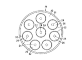
基板25に実装される複数のLED24は、図4に示すように、基板25の中心に1つ、周辺部に複数であって7つがそれぞれ配置されているが、基板25の中心より下部側(下側半分の領域)には上部側(上側半分の領域)に比べてLED24が密に実装されている。すなわち、基板25の周辺部に実装される複数のLED24の周方向のピッチは、基板25の中心より下部側では狭く、上部側では広い関係を有し、また、LED24の数は、基板25の中心より下部側では4つ、上部側では3つで、下部側の方が多い関係を有し、したがって、カバー21の前面から出射される光束の値は、下部側が上部側に比べて大きくなっている。
As shown in FIG. 4, the plurality of
基板25には、この基板25およびレンズホルダ27を放熱体22の前面部35に共締めして固定するねじ38が挿通されるねじ挿通孔53が形成され、放熱体22のアース取付ボス41が挿通されるボス挿通孔54が形成され、レンズホルダ27の位置決め用の複数の位置決め孔55が形成されている。
The
基板25の周辺部には、カバー21と放熱体22とを固定するねじ42が挿通される複数のねじ挿通溝56が形成されている。基板25の上部には放熱体22の配線溝44に対向して連通する電線挿通溝57が形成され、この電線挿通溝57の側部には放熱体22の配線溝44に対向して閉塞する覆い部(遮光部)58が形成されている。電線挿通溝57は配線溝44の後面開口46と互いに対向しない位置に配置され、覆い部58は配線溝44の後面開口46に互いに対向する位置に配置されている。したがって、配線溝44の前面開口45は、基板25の電線挿通溝57に相当する部分が、電線15が通る実質的な前面開口45として構成され、配線溝44の前面開口45と後
面開口46とが直接対向しないように構成されている。
A plurality of screw insertion grooves 56 through which screws 42 for fixing the
また、レンズ26は、例えば、透明な合成樹脂やガラスで形成され、後面にLED24が発光する光がレンズ26内に入射する入射面として形成され、前面にレンズ26内を通過する光が前方へ出射する出射面として形成されている。レンズ26の周辺部にはカバー21のレンズ嵌合孔32とレンズホルダ27との間で挟み込まれて保持されるフランジ60が形成されている。
また、レンズホルダ27は、基板25の前面に取り付けられる基部63、およびこの基部63に一体に設けられた複数の円筒状のホルダ部64を有している。
The
The
基部63には、中心のホルダ部64の周囲で周辺部のホルダ部64との間に、レンズホルダ27および基板25を放熱体22に共締めして固定するねじ38が挿通されるねじ挿通孔65を有するねじ取付ボス66、基板25のコネクタ52に対向して開口するコネクタ接続用開口69、基板25のボス挿通孔54に挿通される放熱体22のアース取付ボス41に対向して開口するアース取付用開口70が形成されている。さらに、レンズホルダ27の上部には、基板25の電線挿通溝57とコネクタ52との間でかつレンズホルダ27の隣り合うホルダ部64間に、電線挿通溝57からコネクタ52へレンズホルダ27の前面側を通じて配線される電線15が嵌り込んで保持する電線保持溝71が形成されている。
基板25に対向する基部63の後面には、基板25の各位置決め孔55に嵌合して位置決めするための図示しない複数の位置決め突起が突設されている。
A screw insertion hole through which a
On the rear surface of the base 63 facing the
なお、レンズホルダ27の各ホルダ部64、カバー21の各レンズ嵌合孔32および各レンズ26は、これらの中心(光軸)が上述した基板25の各LED24の中心位置に対応する位置に配置されている。
The
次に、支持体13は、円筒軸74、この円筒軸74の下端に水平方向に回転可能に取り付けられたアーム75を有し、このアーム75の両端に、灯体12を水平方向の軸で上下方向の角度調整可能に支持している。
円筒軸74内には電源ユニット14に接続された電線15が挿通され、円筒軸74の下端から引き出された電線15が灯体12側に接続されている。
Next, the
An
次に、電源ユニット14は、例えば、LED24に対して電線15を通じて定電流を供給する点灯回路を内蔵している。電線ユニット14は、天井面に直接取り付けられて電源線にて点灯回路に給電されたり、あるいは天井に予め取り付けられた配線レールにより取り付けられるとともに点灯回路に給電されるように構成されている。
Next, the
次に、電線15は、例えば、一対の給電用電線78およびアース線79を1本にまとめた電線であり、一対の給電用電線78の先端には基板25のコネクタ52に接続されるコネクタ80が取り付けられ、アース線79の先端にはアース端子81が取り付けられている。アース端子81は、ねじ82で基板25の前面側に突出するアース取付ボス41に接続固定される。電線15には、先端から所定の長さ位置に電線ホルダ47が取り付けられている。
次に、照明装置11の灯体12の組立について説明する。
Next, the
Next, assembly of the
放熱体22の前面部35を上方へ向けた状態で、この放熱体22の前面部35上にLED24などを実装した基板25を位置決め配置する。このとき、放熱体22の前面部35から突出するアース取付ボス41を基板25のボス挿通孔54に通し、放熱体22の前面部35の凹部35aに基板25を嵌め込んで位置決めする。
With the
放熱体22の前面部35上に配置した基板25上に、レンズホルダ27を配置する。このとき、レンズホルダ27から突出する複数の位置決め突起を基板25の各位置決め孔55に挿入し、レンズホルダ27を基板25および放熱体22に対して位置決めする。
The
ねじ38をレンズホルダ27のねじ取付ボス66に挿入するとともにこのねじ取付ボス66のねじ挿通孔65および基板25のねじ挿通孔53を通じて放熱体22のねじ取付孔39に螺合し、レンズホルダ27および基板25を放熱体22に共締め固定する。これにより、基板25の後面が放熱体22の前面部35に面接触状態に密着し、基板25から放熱体22への熱伝導性が良好になる。
The
この状態で、基板25の電線挿通溝57および覆い部58が放熱体22の配線溝44の前面に対向する位置に配置され、基板25の電線挿通溝57に相当する部分である実質的な前面開口45と後面開口46とが直接対向しないように配線溝44が形成される。また、レンズホルダ27のコネクタ接続用開口69が基板25のコネクタ52に対向し、アース取付用開口70が基板25の前面に突出するアース取付ボス41に対向して配置される。
In this state, the electric
電線15のコネクタ80をレンズホルダ27のコネクタ接続用開口69から基板25のコネクタ52に接続し、アース線79のアース端子81をレンズホルダ27のアース取付用開口70からアース取付ボス41にねじ82で接続固定する。電線15の先端側をレンズホルダ27の前方から電線保持溝71に差し込んで位置決め保持し、さらに、電線15を放熱体22の外側方から配線溝44内に沿って屈曲させながら差し込んで配置し、電線ホルダ47をねじ48で放熱体22の後面に固定する。
一方、カバー21の後面を上方へ向けた状態で、カバー21の各レンズ嵌合孔32に各レンズ26を配置する。
The connector 80 of the
On the other hand, each
レンズ26を配置したカバー21上に、基板25、レンズホルダ27および電線15を取り付けた放熱体22を上方から被せ、レンズホルダ27の各ホルダ部64に各レンズ26を嵌合し、カバー21と放熱体22とを組み合わせる。各ねじ42を放熱体22の取付部43を通じてカバー21に締め付け固定する。
The
これにより、カバー21とレンズホルダ27との間に各レンズ26が挟み込まれて保持され、電線15がカバー21と放熱体22との上部間から外部に引き出され、灯体12の組立が完了する。
Thereby, each
このように、灯体12の組立時において、放熱体22の外側面部36に、この外側面部36から前面部35に亘って連通する配線溝44を設けているため、基板25に接続する電線15を放熱体22の外側から配線溝44に配置するだけで済み、従来のように電線を電線挿通孔に通す手間のかかる作業が必要なくなり、組立作業性を向上できる。
Thus, when the
そして、この灯体12を用いた照明装置11では、電源ユニット14が天井側に取り付けられ、この電源ユニット14に対して円筒軸74およびアーム75により灯体12が支持されている。
In the lighting device 11 using the
電源ユニット14の点灯回路に電源供給することにより、この点灯回路から電線15を通じてLED24に電力供給する。これにより、各LED24が発光し、各LED24の光が各レンズ26を通じて灯体12の前方から投光される。
By supplying power to the lighting circuit of the
この灯体12の点灯時において、放熱体22に配線溝44が設けられていることから、この配線溝44からの光漏れが考えられるが、配線溝44の前面開口45と後面開口46とを互いに前後方向に対向しない位置に設けているため、配線溝44からの光漏れを低減できる。
When the
特に、配線溝44の前面開口45と後面開口46とを互いに前後方向に対向しないようにするのに、放熱体22のみで形成しようとした場合には、放熱体22の配線溝44を製造する金型が複雑化し、放熱体22のコストが高くなるが、放熱体22には配線溝44を略L字形に設けて、この配線溝44の前面を基板25の覆い部58で覆う構造とすることにより、放熱体22の配線溝44を製造する金型が複雑化することなく、低コストで放熱体22を形成できる。
また、LED24が発光時に発生する熱は、主に、基板25から放熱体22に効率よく熱伝導され、この放熱体22の複数の放熱フィン49から空気中に放熱される。
また、支持体13によって、灯体12の前面の向き、つまり光照射方向を水平方向および上下方向に可変して調整することができる。
この場合、放熱体22の上部に配線溝44を設けているため、支持体13に対して灯体12の上下方向の角度を可変調整しても、配線溝44から引き出されている電線15が放熱体22の後部に設けられている放熱フィン49と干渉するのを防止できる。
さらに、放熱体22の放熱フィン49は上下方向に沿って設けられているため、支持体13に対して灯体12の上下方向の角度を可変調整しても、放熱フィン49間に上下方向に沿って流れる対流が生じ、高い放熱効果を維持できる。
また、天井側の高い位置に配置されている照明装置11の灯体12の前面を斜め下方に向けて壁面などの照明対象物を照明するのに使用する場合、この灯体12の前面と照明対象物との距離がその照明対象物の上部側が短く、下部側が上部側よりも長くなり、そのため、照明対象物の下部側が暗くなりやすい。本実施の形態の照明装置11では、基板25の下部側には上部側に比べてLED24を密に実装し、灯体12の前面の下部側から照明対象物の下部側へ出射される光束の値を上部側から照明対象物の上部側へ出射される光束の値に比べて大きくなるため、灯体12との距離の長い照明対象物の下部側も明るくでき、照明対象物の上
下位置での照度を均一にできる。
In particular, in order to prevent the front opening 45 and the
Further, the heat generated when the
Further, the
In this case, since the
Furthermore, since the
In addition, when used to illuminate a lighting object such as a wall surface with the front surface of the
11 照明装置
15 電線
22 放熱体
23 本体
24 半導体発光素子としてLED
25 基板
26 レンズ
27 基板押さえ部材としてのレンズホルダ
35 前面部
44 電線挿通部としての配線溝
49 放熱フィン
11 Lighting equipment
15 Electric wire
22 radiator
23 Body
24 LED as semiconductor light emitting device
25 substrate
26 Lens
27 Lens holder as substrate pressing member
35 Front
44 Wiring groove as wire insertion part
49 Radiating fin
Claims (2)
複数の半導体発光素子それぞれに対応する複数のレンズを含む基板押さえ部材と;
前部に基板が取り付けられる前面部および後部に放熱体が設けられているとともに、前面部には基板の電線をレンズ間によって形成される隙間を経由して後部に挿通する電線挿通部が設けられていて、基板押さえ部材と前面部との間で基板を挟み込んで固定する本体と;
を具備していることを特徴とする照明装置。 A plurality of semiconductor light emitting elements are mounted on at least the peripheral portion and the surface on which the semiconductor light emitting element is mounted , and a connection portion is formed on the inner side of the semiconductor light emitting device mounted on the peripheral portion. A substrate from which is derived;
A substrate pressing member including a plurality of lenses corresponding to each of the plurality of semiconductor light emitting elements;
A heat radiator is provided on the front and rear parts where the board is attached to the front part, and a wire insertion part is provided on the front part for inserting the electric wires of the board into the rear part through a gap formed between the lenses. A body for sandwiching and fixing the substrate between the substrate pressing member and the front surface portion;
An illumination device comprising:
ことを特徴とする請求項1記載の照明装置。 The lighting device according to claim 1, wherein a plurality of heat radiation fins are provided at a rear portion of the heat radiator, and an electric wire is led out from between the heat radiation fins adjacent to each other.
Priority Applications (4)
| Application Number | Priority Date | Filing Date | Title |
|---|---|---|---|
| JP2010014706A JP5445846B2 (en) | 2010-01-26 | 2010-01-26 | Lighting device |
| EP11152025.0A EP2354641A3 (en) | 2010-01-26 | 2011-01-25 | Illumination apparatus |
| US13/013,363 US8727564B2 (en) | 2010-01-26 | 2011-01-25 | Illumination apparatus |
| CN201110031442.9A CN102135260B (en) | 2010-01-26 | 2011-01-26 | Illumination apparatus |
Applications Claiming Priority (1)
| Application Number | Priority Date | Filing Date | Title |
|---|---|---|---|
| JP2010014706A JP5445846B2 (en) | 2010-01-26 | 2010-01-26 | Lighting device |
Publications (3)
| Publication Number | Publication Date |
|---|---|
| JP2011154832A JP2011154832A (en) | 2011-08-11 |
| JP2011154832A5 JP2011154832A5 (en) | 2012-11-08 |
| JP5445846B2 true JP5445846B2 (en) | 2014-03-19 |
Family
ID=44540666
Family Applications (1)
| Application Number | Title | Priority Date | Filing Date |
|---|---|---|---|
| JP2010014706A Expired - Fee Related JP5445846B2 (en) | 2010-01-26 | 2010-01-26 | Lighting device |
Country Status (1)
| Country | Link |
|---|---|
| JP (1) | JP5445846B2 (en) |
Families Citing this family (11)
| Publication number | Priority date | Publication date | Assignee | Title |
|---|---|---|---|---|
| JP2012059636A (en) * | 2010-09-10 | 2012-03-22 | Sharp Corp | Lighting system |
| JP6323740B2 (en) * | 2013-08-28 | 2018-05-16 | パナソニックIpマネジメント株式会社 | lamp |
| JP6198128B2 (en) * | 2013-09-25 | 2017-09-20 | パナソニックIpマネジメント株式会社 | Illumination light source and illumination device |
| JP6187764B2 (en) * | 2014-01-31 | 2017-08-30 | 東芝ライテック株式会社 | Lighting device |
| JP2014132584A (en) * | 2014-02-24 | 2014-07-17 | Sharp Corp | Illumination device |
| JP5763240B1 (en) * | 2014-03-31 | 2015-08-12 | アイリスオーヤマ株式会社 | LED lighting device |
| CN104121512B (en) * | 2014-08-07 | 2017-04-19 | 东莞市闻誉实业有限公司 | LED flexible line lamp |
| JP2015204299A (en) * | 2015-06-23 | 2015-11-16 | アイリスオーヤマ株式会社 | Led lighting device |
| JP6639598B2 (en) * | 2018-09-19 | 2020-02-05 | 三菱電機株式会社 | Lighting equipment |
| JP7218144B2 (en) * | 2018-10-18 | 2023-02-06 | 東海旅客鉄道株式会社 | reading light |
| JP6694604B2 (en) * | 2018-11-09 | 2020-05-20 | 東芝ライテック株式会社 | Lighting equipment |
Family Cites Families (6)
| Publication number | Priority date | Publication date | Assignee | Title |
|---|---|---|---|---|
| JP2006294526A (en) * | 2005-04-14 | 2006-10-26 | Enegate:Kk | Spotlight using led element |
| JP2007087712A (en) * | 2005-09-21 | 2007-04-05 | Toshiba Lighting & Technology Corp | Lamp |
| US7566147B2 (en) * | 2007-05-04 | 2009-07-28 | Ruud Lighting, Inc. | Multi-LED light fixture with secure arrangement for LED-array wiring |
| JP5363462B2 (en) * | 2007-05-07 | 2013-12-11 | コーニンクレッカ フィリップス エヌ ヴェ | LED-based luminaire for surface lighting with improved heat dissipation and manufacturability |
| JP4740964B2 (en) * | 2008-01-11 | 2011-08-03 | 国分電機株式会社 | LED downlight |
| JP4406854B2 (en) * | 2009-06-24 | 2010-02-03 | 東芝ライテック株式会社 | Light emitting element lamp and lighting apparatus |
-
2010
- 2010-01-26 JP JP2010014706A patent/JP5445846B2/en not_active Expired - Fee Related
Also Published As
| Publication number | Publication date |
|---|---|
| JP2011154832A (en) | 2011-08-11 |
Similar Documents
| Publication | Publication Date | Title |
|---|---|---|
| JP5445846B2 (en) | Lighting device | |
| US8727564B2 (en) | Illumination apparatus | |
| JP2011154832A5 (en) | ||
| JP5320555B2 (en) | Light emitting element lamp and lighting apparatus | |
| JP5614794B2 (en) | Lighting device | |
| JP2007324137A (en) | Lighting system | |
| US8803409B1 (en) | Lamp device, light-emitting device and luminaire | |
| JP4406854B2 (en) | Light emitting element lamp and lighting apparatus | |
| JP2009129809A (en) | Lighting system | |
| JP2010073654A (en) | Luminaire | |
| JP2011159447A (en) | Lighting system | |
| JP2010135747A (en) | Light-emitting module and lighting apparatus | |
| JP5630624B2 (en) | Lighting device | |
| US20110205741A1 (en) | Lighting equipment | |
| KR20130128623A (en) | Lighting apparatus | |
| JP2010170903A (en) | Socket for light source, and lighting fixture | |
| JP5494867B1 (en) | Light source unit and lighting device | |
| JP2008166097A (en) | Lighting fixture | |
| JP2011216313A (en) | Luminaire | |
| JP2011181252A (en) | Lighting fixture | |
| JP2011029065A (en) | Led lighting apparatus | |
| JP6624546B2 (en) | lighting equipment | |
| JP2008300207A (en) | Lighting device | |
| JP2015212997A (en) | Lighting device | |
| JP6592785B2 (en) | Lighting lamp |
Legal Events
| Date | Code | Title | Description |
|---|---|---|---|
| A521 | Written amendment |
Free format text: JAPANESE INTERMEDIATE CODE: A523 Effective date: 20120921 |
|
| A621 | Written request for application examination |
Free format text: JAPANESE INTERMEDIATE CODE: A621 Effective date: 20120921 |
|
| A871 | Explanation of circumstances concerning accelerated examination |
Free format text: JAPANESE INTERMEDIATE CODE: A871 Effective date: 20130415 |
|
| A975 | Report on accelerated examination |
Free format text: JAPANESE INTERMEDIATE CODE: A971005 Effective date: 20130423 |
|
| A131 | Notification of reasons for refusal |
Free format text: JAPANESE INTERMEDIATE CODE: A131 Effective date: 20130501 |
|
| A521 | Written amendment |
Free format text: JAPANESE INTERMEDIATE CODE: A523 Effective date: 20130531 |
|
| A02 | Decision of refusal |
Free format text: JAPANESE INTERMEDIATE CODE: A02 Effective date: 20130619 |
|
| A521 | Written amendment |
Free format text: JAPANESE INTERMEDIATE CODE: A523 Effective date: 20130919 |
|
| A911 | Transfer of reconsideration by examiner before appeal (zenchi) |
Free format text: JAPANESE INTERMEDIATE CODE: A911 Effective date: 20130926 |
|
| TRDD | Decision of grant or rejection written | ||
| A01 | Written decision to grant a patent or to grant a registration (utility model) |
Free format text: JAPANESE INTERMEDIATE CODE: A01 Effective date: 20131128 |
|
| A61 | First payment of annual fees (during grant procedure) |
Free format text: JAPANESE INTERMEDIATE CODE: A61 Effective date: 20131211 |
|
| LAPS | Cancellation because of no payment of annual fees |