JP5441332B2 - Endpoint detection for photomask etching - Google Patents
Endpoint detection for photomask etching Download PDFInfo
- Publication number
- JP5441332B2 JP5441332B2 JP2007278649A JP2007278649A JP5441332B2 JP 5441332 B2 JP5441332 B2 JP 5441332B2 JP 2007278649 A JP2007278649 A JP 2007278649A JP 2007278649 A JP2007278649 A JP 2007278649A JP 5441332 B2 JP5441332 B2 JP 5441332B2
- Authority
- JP
- Japan
- Prior art keywords
- substrate
- etching
- signal
- window
- light
- Prior art date
- Legal status (The legal status is an assumption and is not a legal conclusion. Google has not performed a legal analysis and makes no representation as to the accuracy of the status listed.)
- Active
Links
- 238000005530 etching Methods 0.000 title claims abstract description 173
- 238000001514 detection method Methods 0.000 title claims abstract description 128
- 239000000758 substrate Substances 0.000 claims abstract description 211
- 238000000034 method Methods 0.000 claims abstract description 100
- 230000003287 optical effect Effects 0.000 claims abstract description 90
- 230000008569 process Effects 0.000 claims abstract description 57
- 238000012545 processing Methods 0.000 claims description 68
- VYZAMTAEIAYCRO-UHFFFAOYSA-N Chromium Chemical compound [Cr] VYZAMTAEIAYCRO-UHFFFAOYSA-N 0.000 claims description 50
- 239000011651 chromium Substances 0.000 claims description 40
- 229910052804 chromium Inorganic materials 0.000 claims description 29
- 230000002093 peripheral effect Effects 0.000 claims description 29
- 239000013307 optical fiber Substances 0.000 claims description 25
- 230000005855 radiation Effects 0.000 claims description 13
- 239000010409 thin film Substances 0.000 claims description 9
- 230000008878 coupling Effects 0.000 claims description 6
- 238000010168 coupling process Methods 0.000 claims description 6
- 238000005859 coupling reaction Methods 0.000 claims description 6
- 238000001020 plasma etching Methods 0.000 claims description 6
- 230000004044 response Effects 0.000 claims description 5
- 238000004458 analytical method Methods 0.000 claims description 3
- 230000005469 synchrotron radiation Effects 0.000 claims description 2
- 238000003672 processing method Methods 0.000 claims 1
- 238000012544 monitoring process Methods 0.000 abstract description 68
- 238000000691 measurement method Methods 0.000 abstract description 3
- 230000005540 biological transmission Effects 0.000 description 45
- 239000000835 fiber Substances 0.000 description 40
- 229920002120 photoresistant polymer Polymers 0.000 description 37
- 238000004993 emission spectroscopy Methods 0.000 description 29
- 238000005259 measurement Methods 0.000 description 24
- 239000007789 gas Substances 0.000 description 22
- 238000002834 transmittance Methods 0.000 description 22
- VYPSYNLAJGMNEJ-UHFFFAOYSA-N silicon dioxide Inorganic materials O=[Si]=O VYPSYNLAJGMNEJ-UHFFFAOYSA-N 0.000 description 16
- 239000010453 quartz Substances 0.000 description 15
- 235000012431 wafers Nutrition 0.000 description 15
- 230000008859 change Effects 0.000 description 14
- 239000000463 material Substances 0.000 description 14
- 238000013461 design Methods 0.000 description 12
- 238000004519 manufacturing process Methods 0.000 description 11
- 238000005070 sampling Methods 0.000 description 11
- 238000012360 testing method Methods 0.000 description 11
- 230000008901 benefit Effects 0.000 description 10
- YXTPWUNVHCYOSP-UHFFFAOYSA-N bis($l^{2}-silanylidene)molybdenum Chemical compound [Si]=[Mo]=[Si] YXTPWUNVHCYOSP-UHFFFAOYSA-N 0.000 description 9
- 229910021344 molybdenum silicide Inorganic materials 0.000 description 9
- 238000010586 diagram Methods 0.000 description 8
- 238000001228 spectrum Methods 0.000 description 8
- 230000007423 decrease Effects 0.000 description 7
- 239000010408 film Substances 0.000 description 7
- 230000006870 function Effects 0.000 description 7
- 229910052751 metal Inorganic materials 0.000 description 6
- 239000002184 metal Substances 0.000 description 6
- 239000000460 chlorine Substances 0.000 description 5
- 238000005305 interferometry Methods 0.000 description 5
- 230000010363 phase shift Effects 0.000 description 5
- 238000004886 process control Methods 0.000 description 5
- 230000003595 spectral effect Effects 0.000 description 5
- 238000010521 absorption reaction Methods 0.000 description 4
- 238000004364 calculation method Methods 0.000 description 4
- 238000000151 deposition Methods 0.000 description 4
- 230000008021 deposition Effects 0.000 description 4
- 239000006185 dispersion Substances 0.000 description 4
- 239000000523 sample Substances 0.000 description 4
- ZAMOUSCENKQFHK-UHFFFAOYSA-N Chlorine atom Chemical compound [Cl] ZAMOUSCENKQFHK-UHFFFAOYSA-N 0.000 description 3
- 238000013459 approach Methods 0.000 description 3
- 229910052801 chlorine Inorganic materials 0.000 description 3
- 238000009826 distribution Methods 0.000 description 3
- 238000005516 engineering process Methods 0.000 description 3
- 238000003384 imaging method Methods 0.000 description 3
- 230000006872 improvement Effects 0.000 description 3
- 230000000670 limiting effect Effects 0.000 description 3
- 238000001459 lithography Methods 0.000 description 3
- 238000010606 normalization Methods 0.000 description 3
- NJPPVKZQTLUDBO-UHFFFAOYSA-N novaluron Chemical compound C1=C(Cl)C(OC(F)(F)C(OC(F)(F)F)F)=CC=C1NC(=O)NC(=O)C1=C(F)C=CC=C1F NJPPVKZQTLUDBO-UHFFFAOYSA-N 0.000 description 3
- 239000000047 product Substances 0.000 description 3
- 230000002829 reductive effect Effects 0.000 description 3
- YZCKVEUIGOORGS-OUBTZVSYSA-N Deuterium Chemical compound [2H] YZCKVEUIGOORGS-OUBTZVSYSA-N 0.000 description 2
- XPDWGBQVDMORPB-UHFFFAOYSA-N Fluoroform Chemical compound FC(F)F XPDWGBQVDMORPB-UHFFFAOYSA-N 0.000 description 2
- XUIMIQQOPSSXEZ-UHFFFAOYSA-N Silicon Chemical compound [Si] XUIMIQQOPSSXEZ-UHFFFAOYSA-N 0.000 description 2
- 230000002745 absorbent Effects 0.000 description 2
- 239000002250 absorbent Substances 0.000 description 2
- 229910052782 aluminium Inorganic materials 0.000 description 2
- XAGFODPZIPBFFR-UHFFFAOYSA-N aluminium Chemical compound [Al] XAGFODPZIPBFFR-UHFFFAOYSA-N 0.000 description 2
- 238000009529 body temperature measurement Methods 0.000 description 2
- 238000004422 calculation algorithm Methods 0.000 description 2
- 238000006243 chemical reaction Methods 0.000 description 2
- 229910052805 deuterium Inorganic materials 0.000 description 2
- 230000005684 electric field Effects 0.000 description 2
- 239000011521 glass Substances 0.000 description 2
- 230000006698 induction Effects 0.000 description 2
- 238000004020 luminiscence type Methods 0.000 description 2
- 239000000203 mixture Substances 0.000 description 2
- 239000000376 reactant Substances 0.000 description 2
- 238000002310 reflectometry Methods 0.000 description 2
- 229910052710 silicon Inorganic materials 0.000 description 2
- 239000010703 silicon Substances 0.000 description 2
- 239000007787 solid Substances 0.000 description 2
- 230000003068 static effect Effects 0.000 description 2
- MYMOFIZGZYHOMD-UHFFFAOYSA-N Dioxygen Chemical compound O=O MYMOFIZGZYHOMD-UHFFFAOYSA-N 0.000 description 1
- YCKRFDGAMUMZLT-UHFFFAOYSA-N Fluorine atom Chemical compound [F] YCKRFDGAMUMZLT-UHFFFAOYSA-N 0.000 description 1
- WGLPBDUCMAPZCE-UHFFFAOYSA-N Trioxochromium Chemical compound O=[Cr](=O)=O WGLPBDUCMAPZCE-UHFFFAOYSA-N 0.000 description 1
- 238000002835 absorbance Methods 0.000 description 1
- 239000006096 absorbing agent Substances 0.000 description 1
- 230000002411 adverse Effects 0.000 description 1
- 230000002238 attenuated effect Effects 0.000 description 1
- 230000009286 beneficial effect Effects 0.000 description 1
- 230000008033 biological extinction Effects 0.000 description 1
- 239000006227 byproduct Substances 0.000 description 1
- 239000000919 ceramic Substances 0.000 description 1
- 229910000423 chromium oxide Inorganic materials 0.000 description 1
- 238000005352 clarification Methods 0.000 description 1
- 238000004140 cleaning Methods 0.000 description 1
- 239000011248 coating agent Substances 0.000 description 1
- 238000000576 coating method Methods 0.000 description 1
- 150000001875 compounds Chemical class 0.000 description 1
- 238000004590 computer program Methods 0.000 description 1
- 239000004020 conductor Substances 0.000 description 1
- 238000012790 confirmation Methods 0.000 description 1
- 238000013480 data collection Methods 0.000 description 1
- 230000001066 destructive effect Effects 0.000 description 1
- 238000002050 diffraction method Methods 0.000 description 1
- 238000009792 diffusion process Methods 0.000 description 1
- 229910001882 dioxygen Inorganic materials 0.000 description 1
- 238000001312 dry etching Methods 0.000 description 1
- 230000009977 dual effect Effects 0.000 description 1
- 230000000694 effects Effects 0.000 description 1
- 238000010894 electron beam technology Methods 0.000 description 1
- 239000000284 extract Substances 0.000 description 1
- 229910052731 fluorine Inorganic materials 0.000 description 1
- 239000011737 fluorine Substances 0.000 description 1
- 239000005350 fused silica glass Substances 0.000 description 1
- 238000009499 grossing Methods 0.000 description 1
- 229910052736 halogen Inorganic materials 0.000 description 1
- 150000002367 halogens Chemical class 0.000 description 1
- 229910052739 hydrogen Inorganic materials 0.000 description 1
- 150000002431 hydrogen Chemical class 0.000 description 1
- 239000001257 hydrogen Substances 0.000 description 1
- 238000011065 in-situ storage Methods 0.000 description 1
- 238000009616 inductively coupled plasma Methods 0.000 description 1
- 238000009434 installation Methods 0.000 description 1
- 238000009413 insulation Methods 0.000 description 1
- 230000010354 integration Effects 0.000 description 1
- 230000003993 interaction Effects 0.000 description 1
- 238000005468 ion implantation Methods 0.000 description 1
- 238000002955 isolation Methods 0.000 description 1
- 238000013507 mapping Methods 0.000 description 1
- 230000007246 mechanism Effects 0.000 description 1
- 238000004377 microelectronic Methods 0.000 description 1
- 239000000615 nonconductor Substances 0.000 description 1
- 230000003647 oxidation Effects 0.000 description 1
- 238000007254 oxidation reaction Methods 0.000 description 1
- 238000003825 pressing Methods 0.000 description 1
- 230000009467 reduction Effects 0.000 description 1
- 229920006395 saturated elastomer Polymers 0.000 description 1
- 238000007789 sealing Methods 0.000 description 1
- 239000004065 semiconductor Substances 0.000 description 1
- 230000008054 signal transmission Effects 0.000 description 1
- 238000000992 sputter etching Methods 0.000 description 1
- 239000000126 substance Substances 0.000 description 1
- TXEYQDLBPFQVAA-UHFFFAOYSA-N tetrafluoromethane Chemical compound FC(F)(F)F TXEYQDLBPFQVAA-UHFFFAOYSA-N 0.000 description 1
- 238000000427 thin-film deposition Methods 0.000 description 1
- 238000012876 topography Methods 0.000 description 1
- 238000012546 transfer Methods 0.000 description 1
- 238000000411 transmission spectrum Methods 0.000 description 1
- 239000013598 vector Substances 0.000 description 1
- 238000001039 wet etching Methods 0.000 description 1
Images


Classifications
-
- H—ELECTRICITY
- H01—ELECTRIC ELEMENTS
- H01L—SEMICONDUCTOR DEVICES NOT COVERED BY CLASS H10
- H01L21/00—Processes or apparatus adapted for the manufacture or treatment of semiconductor or solid state devices or of parts thereof
- H01L21/02—Manufacture or treatment of semiconductor devices or of parts thereof
- H01L21/04—Manufacture or treatment of semiconductor devices or of parts thereof the devices having at least one potential-jump barrier or surface barrier, e.g. PN junction, depletion layer or carrier concentration layer
- H01L21/18—Manufacture or treatment of semiconductor devices or of parts thereof the devices having at least one potential-jump barrier or surface barrier, e.g. PN junction, depletion layer or carrier concentration layer the devices having semiconductor bodies comprising elements of Group IV of the Periodic System or AIIIBV compounds with or without impurities, e.g. doping materials
- H01L21/30—Treatment of semiconductor bodies using processes or apparatus not provided for in groups H01L21/20 - H01L21/26
- H01L21/302—Treatment of semiconductor bodies using processes or apparatus not provided for in groups H01L21/20 - H01L21/26 to change their surface-physical characteristics or shape, e.g. etching, polishing, cutting
- H01L21/306—Chemical or electrical treatment, e.g. electrolytic etching
- H01L21/3065—Plasma etching; Reactive-ion etching
-
- H—ELECTRICITY
- H01—ELECTRIC ELEMENTS
- H01L—SEMICONDUCTOR DEVICES NOT COVERED BY CLASS H10
- H01L21/00—Processes or apparatus adapted for the manufacture or treatment of semiconductor or solid state devices or of parts thereof
- H01L21/67—Apparatus specially adapted for handling semiconductor or electric solid state devices during manufacture or treatment thereof; Apparatus specially adapted for handling wafers during manufacture or treatment of semiconductor or electric solid state devices or components ; Apparatus not specifically provided for elsewhere
- H01L21/67005—Apparatus not specifically provided for elsewhere
- H01L21/67242—Apparatus for monitoring, sorting or marking
- H01L21/67253—Process monitoring, e.g. flow or thickness monitoring
-
- G—PHYSICS
- G03—PHOTOGRAPHY; CINEMATOGRAPHY; ANALOGOUS TECHNIQUES USING WAVES OTHER THAN OPTICAL WAVES; ELECTROGRAPHY; HOLOGRAPHY
- G03F—PHOTOMECHANICAL PRODUCTION OF TEXTURED OR PATTERNED SURFACES, e.g. FOR PRINTING, FOR PROCESSING OF SEMICONDUCTOR DEVICES; MATERIALS THEREFOR; ORIGINALS THEREFOR; APPARATUS SPECIALLY ADAPTED THEREFOR
- G03F1/00—Originals for photomechanical production of textured or patterned surfaces, e.g., masks, photo-masks, reticles; Mask blanks or pellicles therefor; Containers specially adapted therefor; Preparation thereof
- G03F1/68—Preparation processes not covered by groups G03F1/20 - G03F1/50
- G03F1/80—Etching
-
- H—ELECTRICITY
- H01—ELECTRIC ELEMENTS
- H01L—SEMICONDUCTOR DEVICES NOT COVERED BY CLASS H10
- H01L21/00—Processes or apparatus adapted for the manufacture or treatment of semiconductor or solid state devices or of parts thereof
- H01L21/02—Manufacture or treatment of semiconductor devices or of parts thereof
- H01L21/04—Manufacture or treatment of semiconductor devices or of parts thereof the devices having at least one potential-jump barrier or surface barrier, e.g. PN junction, depletion layer or carrier concentration layer
- H01L21/18—Manufacture or treatment of semiconductor devices or of parts thereof the devices having at least one potential-jump barrier or surface barrier, e.g. PN junction, depletion layer or carrier concentration layer the devices having semiconductor bodies comprising elements of Group IV of the Periodic System or AIIIBV compounds with or without impurities, e.g. doping materials
- H01L21/30—Treatment of semiconductor bodies using processes or apparatus not provided for in groups H01L21/20 - H01L21/26
- H01L21/302—Treatment of semiconductor bodies using processes or apparatus not provided for in groups H01L21/20 - H01L21/26 to change their surface-physical characteristics or shape, e.g. etching, polishing, cutting
- H01L21/306—Chemical or electrical treatment, e.g. electrolytic etching
-
- H—ELECTRICITY
- H01—ELECTRIC ELEMENTS
- H01L—SEMICONDUCTOR DEVICES NOT COVERED BY CLASS H10
- H01L21/00—Processes or apparatus adapted for the manufacture or treatment of semiconductor or solid state devices or of parts thereof
- H01L21/67—Apparatus specially adapted for handling semiconductor or electric solid state devices during manufacture or treatment thereof; Apparatus specially adapted for handling wafers during manufacture or treatment of semiconductor or electric solid state devices or components ; Apparatus not specifically provided for elsewhere
- H01L21/67005—Apparatus not specifically provided for elsewhere
- H01L21/67011—Apparatus for manufacture or treatment
- H01L21/67017—Apparatus for fluid treatment
- H01L21/67063—Apparatus for fluid treatment for etching
- H01L21/67069—Apparatus for fluid treatment for etching for drying etching
-
- H—ELECTRICITY
- H01—ELECTRIC ELEMENTS
- H01L—SEMICONDUCTOR DEVICES NOT COVERED BY CLASS H10
- H01L22/00—Testing or measuring during manufacture or treatment; Reliability measurements, i.e. testing of parts without further processing to modify the parts as such; Structural arrangements therefor
-
- H—ELECTRICITY
- H01—ELECTRIC ELEMENTS
- H01L—SEMICONDUCTOR DEVICES NOT COVERED BY CLASS H10
- H01L22/00—Testing or measuring during manufacture or treatment; Reliability measurements, i.e. testing of parts without further processing to modify the parts as such; Structural arrangements therefor
- H01L22/20—Sequence of activities consisting of a plurality of measurements, corrections, marking or sorting steps
- H01L22/26—Acting in response to an ongoing measurement without interruption of processing, e.g. endpoint detection, in-situ thickness measurement
-
- H—ELECTRICITY
- H01—ELECTRIC ELEMENTS
- H01L—SEMICONDUCTOR DEVICES NOT COVERED BY CLASS H10
- H01L2924/00—Indexing scheme for arrangements or methods for connecting or disconnecting semiconductor or solid-state bodies as covered by H01L24/00
- H01L2924/0001—Technical content checked by a classifier
- H01L2924/0002—Not covered by any one of groups H01L24/00, H01L24/00 and H01L2224/00
Abstract
Description
(発明の分野)
本発明は、概して、集積回路の製作と集積回路の製造に有用なフォトマスクの製作に関する。
(Field of Invention)
The present invention relates generally to the fabrication of integrated circuits and the production of photomasks useful in the manufacture of integrated circuits.
(関連技術の説明)
マイクロエレクトロニクス又は集積回路デバイスの製作は、典型的には、半導体、誘電性又は導電性基板に施す数百もの個別工程を必要とする複雑な処理シーケンスを伴う。これらの処理工程の例には酸化、拡散、イオン注入、薄膜蒸着、洗浄、エッチング、リソグラフィが含まれる。リソグラフィとエッチング(パターン転写工程と呼ばれることが多い)を用い、まず、所望のパターンを感光性材料層、例えばフォトレジストに転写し、その後、次のエッチング中にその下の材料層に転写する。リソグラフィ工程で、ブランケットフォトレジスト層をパターンを含むレチクル又はフォトマスクを介して放射光源に曝露すると、パターンの像がフォトレジストに形成される。適切な化学溶液中でフォトレジストを現像するとフォトレジストの一部が除去され、パターン形成されたフォトレジスト層が得られる。このフォトレジストパターンをマスクとして用いて、その下の材料層を、例えばウェット又はドライエッチングにより反応環境に曝露すると、その下の材料層にパターンが転写される。
(Description of related technology)
Fabrication of microelectronics or integrated circuit devices typically involves complex processing sequences that require hundreds of individual processes to be performed on a semiconductor, dielectric or conductive substrate. Examples of these processing steps include oxidation, diffusion, ion implantation, thin film deposition, cleaning, etching, and lithography. Using lithography and etching (often referred to as a pattern transfer process), a desired pattern is first transferred to a photosensitive material layer, such as a photoresist, and then transferred to the underlying material layer during the next etching. In a lithographic process, an image of the pattern is formed in the photoresist when the blanket photoresist layer is exposed to a radiation source through a reticle or photomask containing the pattern. Developing the photoresist in a suitable chemical solution removes a portion of the photoresist and results in a patterned photoresist layer. When this photoresist pattern is used as a mask and the underlying material layer is exposed to a reaction environment, for example, by wet or dry etching, the pattern is transferred to the underlying material layer.
典型的にはガラス又は石英基板上に支持された金属含有層に形成されるフォトマスク上のパターンは、フォトレジストパターンを介してエッチングすることでも形成できる。しかしながら、この場合、フォトレジストパターンをレチクルを介したフォトレジストの曝露とは対照的に、例えば電子ビーム又はその他の適切な照射ビームを用いて直接書込み法により形成する。パターン形成したフォトレジストをマスクとして使用し、パターンをその下の金属含有層にプラズマエッチングを用いて転写可能である。最新のデバイス製造での使用に適した市販のフォトマスクエッチング機器の一例としては、カリフォルニア州サンタクララのアプライドマテリアル社から入手可能なテトラ(Tetra(商標名))フォトマスクエッチシステムが挙げられる。「マスク」「フォトマスク」又は「レチクル」という用語は、パターンを含む基板を総称して同じ意味で用いられる。 Typically, a pattern on a photomask formed in a metal-containing layer supported on a glass or quartz substrate can also be formed by etching through a photoresist pattern. However, in this case, the photoresist pattern is formed by direct writing, for example using an electron beam or other suitable irradiation beam, as opposed to exposing the photoresist through the reticle. The patterned photoresist can be used as a mask and the pattern transferred to the underlying metal-containing layer using plasma etching. An example of a commercially available photomask etching equipment suitable for use in modern device manufacturing is the Tetra ™ photomask etch system available from Applied Materials, Inc., Santa Clara, California. The terms “mask”, “photomask”, and “reticle” are used interchangeably to refer collectively to a substrate that includes a pattern.
処理中、フォトマスクのエッチングからの終点データを用いて処理が所要規格に沿って行われているか否か、及びエッチング均一性等の所望の結果が達成されたか否かを求めることができる。各フォトマスクは、通常、一連の独自の特徴部又はパターンを有するため、同一のプロセスレシピを用いてエッチングしたフォトマスクの終点データはフォトマスクごとに異なり、所望のエッチング結果が特定のフォトマスクについて得られたか否かを測定するのは困難である。 During processing, end point data from photomask etching can be used to determine whether the processing is in compliance with the required standards and whether desired results such as etching uniformity have been achieved. Each photomask typically has a unique set of features or patterns, so the photomask endpoint data etched using the same process recipe varies from photomask to photomask, and the desired etch results for a particular photomask. It is difficult to measure whether it has been obtained.
デバイス寸法がますます小型化するにつれ、先端技術に向けたフォトマスクのデザインと製造は一層複雑になってきており、限界寸法や処理の均一性の制御は一段と重要になってきている。従って、各フォトマスクについて一貫した終点データを生成するための改善された装置及び方法等の、フォトマスク製造における処理制御の改善が現在求められている。 As device dimensions continue to shrink, the design and manufacture of photomasks for advanced technologies has become more complex, and control of critical dimensions and process uniformity has become increasingly important. Accordingly, there is a current need for improved process control in photomask manufacturing, such as improved apparatus and methods for generating consistent endpoint data for each photomask.
本発明の実施形態は基板のエッチング方法及び装置を提供する。本発明は真空処理で使用されるその他の基板の中でもフォトマスクのエッチングに特に適している。 Embodiments of the present invention provide a method and apparatus for etching a substrate. The present invention is particularly suitable for photomask etching among other substrates used in vacuum processing.
一実施形態において、(a)少なくとも中央領域の第1窓部と周辺領域の第2窓部を備える基板支持部材を有するエッチングチャンバを設置し、(b)基板を基板支持部材上に載置し、(c)処理ガスをエッチングチャンバ内に導入し、(d)基板をエッチングするために処理ガスからプラズマを発生させ、(e)終点検出システムを用いて第1窓部を通して第1光信号を、第2窓部を通して第2光信号を検出し、検出した第1及び第2光信号の少なくとも1つから得た情報に基づいてプラズマを終了させることを含む基板エッチング方法を提供する。 In one embodiment, (a) an etching chamber having a substrate support member having at least a first window portion in the central region and a second window portion in the peripheral region is installed, and (b) the substrate is placed on the substrate support member. (C) introducing a processing gas into the etching chamber; (d) generating a plasma from the processing gas to etch the substrate; and (e) generating a first optical signal through the first window using an endpoint detection system. And a substrate etching method including detecting a second optical signal through the second window and terminating the plasma based on information obtained from at least one of the detected first and second optical signals.
別の実施形態において、基板エッチング方法は(a)第1窓部と第2窓部を有する基板支持部材を有するエッチングチャンバを設置し、(b)基板を基板支持部材上に載置し、(c)基板をエッチングするために処理ガスからプラズマを発生させ、(d)光検出装置を備えた終点検出システムを設置し、(e)光検出装置を用いて第1窓部及び第2窓部の少なくとも1つを通して少なくとも1つの光信号を監視し、(f)少なくとも1つの光信号から得た情報に基づいてプラズマを終了させることを含む。 In another embodiment, the substrate etching method includes: (a) installing an etching chamber having a substrate support member having a first window portion and a second window portion; (b) placing the substrate on the substrate support member; c) Plasma is generated from the processing gas to etch the substrate, (d) an end point detection system including a photodetection device is installed, and (e) a first window portion and a second window portion using the photodetection device. Monitoring at least one optical signal through at least one of: and (f) terminating the plasma based on information obtained from the at least one optical signal.
本発明の別の実施形態において、プラズマエッチングチャンバと、チャンバ内の、中央領域に配置された第1窓部と周辺領域に配置された第2窓部を有する基板支持部材と、第1及び第2窓部を通してチャンバと連動する終点検出システムを含む基板エッチング装置を提供する。 In another embodiment of the present invention, a plasma etching chamber, a substrate support member having a first window disposed in a central region and a second window disposed in a peripheral region, and first and first chambers in the chamber. A substrate etching apparatus is provided that includes an end point detection system that operates in conjunction with a chamber through two windows.
別の実施形態において、基板エッチング装置は基板支持部材と、反射モード又は透過モードの少なくとも1つで運転するように構成された終点検出システムを含み、終点検出システムは基板支持部材の中央領域に配置された第1光学部品と基板支持部材の周辺領域に配置された第2光学部品を備える。 In another embodiment, the substrate etching apparatus includes a substrate support member and an endpoint detection system configured to operate in at least one of a reflection mode or a transmission mode, the endpoint detection system disposed in a central region of the substrate support member. A first optical component and a second optical component disposed in a peripheral region of the substrate support member.
別の実施形態はプラズマエッチングチャンバと、第1及び第2窓部を有し、第1窓部がその中央領域に在るチャンバ内の基板支持部材と、第1及び第2窓部の1つを通してチャンバと連動している終点検出システムを含む基板エッチング装置を提供する。 Another embodiment includes a plasma etching chamber and a substrate support member in the chamber having first and second windows, the first window being in a central region thereof, and one of the first and second windows. A substrate etching apparatus is provided that includes an endpoint detection system in conjunction with the chamber.
別の実施形態においては、基板エッチング方法は中央領域に第1窓部を、周辺領域に第2窓部を備える基板支持部材を有するエッチングチャンバを設置し、基板を基板支持部材上に載置し、エッチングチャンバ内に処理ガスを導入し、基板をエッチングするために処理ガスからプラズマを発生させ、終点検出システムを用いて第1窓部を通して第1光信号を、第2窓部を通して第2光信号を検出し、検出した第1及び第2光学信号の少なくとも1つから得た情報に基づいてプラズマを終了させることを含む。 In another embodiment, the substrate etching method includes installing an etching chamber having a substrate support member having a first window portion in a central region and a second window portion in a peripheral region, and placing the substrate on the substrate support member. A process gas is introduced into the etching chamber, a plasma is generated from the process gas to etch the substrate, a first optical signal is transmitted through the first window using an end point detection system, and a second light is transmitted through the second window. Detecting a signal and terminating the plasma based on information obtained from at least one of the detected first and second optical signals.
更に別の実施形態において、基板エッチング方法は(a)第1窓部及び第2窓部を有する基板支持部材を有するエッチングチャンバを設置し、(b)基板を基板支持部材上に載置し、(d)基板をエッチングするために処理ガスからプラズマを発生させ、(e)光検出装置を含む終点検出システムを設置し、(f)光検出装置を用いて第1窓部及び第2窓部の少なくとも1つを通して少なくとも1つの光信号を監視し、(g)少なくとも1つの光信号から得た情報に基づいてプラズマを終了させることを含む。 In yet another embodiment, the substrate etching method includes: (a) installing an etching chamber having a substrate support member having a first window portion and a second window portion; (b) placing the substrate on the substrate support member; (D) Plasma is generated from the processing gas to etch the substrate, (e) an end point detection system including a photodetection device is installed, and (f) a first window portion and a second window portion using the photodetection device. Monitoring at least one optical signal through at least one of: and (g) terminating the plasma based on information obtained from the at least one optical signal.
本発明は、例えばフォトマスクの異なる領域を光学的に監視することで、向上した処理監視でもってフォトマスク基板をエッチングするための方法及び装置を提供する。説明及び実例はフォトマスク基板のエッチングに焦点をあてたものであるが、本発明の多様な実施形態は透明又は誘電性基板を含むその他の適切な基板の処理監視にも適合可能である。 The present invention provides a method and apparatus for etching a photomask substrate with improved process monitoring, for example, by optically monitoring different regions of the photomask. Although the description and illustrations focus on photomask substrate etching, various embodiments of the present invention are also adaptable to process monitoring of other suitable substrates, including transparent or dielectric substrates.
図1Aは本発明の一実施形態によるプラズマエッチングチャンバ10の概略断面図である。適切なプラズマエッチングチャンバにはカリフォルニア州サンタクララのアプライドマテリアル社から入手可能なテトラ(商標名)II(Tetra)フォトマスクエッチチャンバ又は分離プラズマソース(DPS(商標名))が含まれる。異なるデザインの誘導結合プラズマエッチングチャンバのみならず例えば容量結合平行板型チャンバ及び磁気強化型イオンエッチングチャンバを含め、その他の処理チャンバも本発明の実施形態と関連して使用することができる。図1で図示の特定の実施形態のエッチングチャンバ10は例示を目的としたものであり、本発明の範囲を制限するものとして使用されるべきではない。その他の製造業者によるものを含め、本発明をその他の処理システムでも利用することも想定される。
FIG. 1A is a schematic cross-sectional view of a
処理チャンバ10は、通常、円筒形の側壁つまりチャンバ本体部12と、本体部12上に取り付けられたエネルギー透過性天井部13と、チャンバ底部17を含む。天井部13は平面、矩形、弓形、円錐形、ドーム状又は複合半径形状であってもよい。少なくとも1つの誘導コイル26が天井部13の少なくとも一部の上方に配置されている。図1Aの実施形態においては2本の同心コイル26が図示されている。処理チャンバ10のチャンバ本体部12とチャンバ底部17は陽極酸化アルミニウム等の金属から形成可能であり、天井部13はセラミック又はその他の誘電体等のエネルギー透過性材料から形成可能である。
The
基板支持部材16が処理チャンバ10内に配置されており、処理中、基板220を支持する。支持部材16は少なくともその一部が導電性であり、処理バイアス印加電極として機能可能な慣用のメカニカル又は静電チャックであってもよい。図示されてはいないが、フォトマスクアダプタを用いてフォトマスクを支持部材16に固定してもよい。フォトマスクアダプタは、通常、支持部材の上部を覆うように加工された下部と、フォトマスクを保持するようなサイズと形状の開口部を有する最上部を含む。一実施形態において、フォトマスクアダプタの最上部は正方形の開口部を有する。適切なフォトマスクアダプタは2001年6月26日に発行の米国特許第6251217号に開示されている。
A
処理ガスは支持部材16近傍の周縁域に配置されたガス分配装置22を介して処理ガス供給源48から処理チャンバ10へと導入される。各処理ガス又は処理ガス混合物の質量流量制御装置(図示せず)が処理チャンバ10と処理ガス供給源48との間に配置され、処理ガスの各流量を調整する。
The processing gas is introduced from the processing
プラズマ域14は処理チャンバ10、基板支持部材16、及び天井部13により規定される。プラズマは、電源27から誘導コイル26へとRF整合回路35を経由して電力を供給することにより、プラズマ域14内で処理ガスから発生させられる。支持部材16はその内部に電極を含んでいてもよく、電極は電極電源28により給電され、RF整合回路25を経由して処理チャンバ10内で容量性電界を発生させる。典型的には、本体部12を電気的に接地しながら、RF電力を支持部材16の電極に印加する。支持部材16の面を横断する容量性電界は荷電種の指向性に影響を及ぼし、基板220のエッチングがより異方性となる。
The
処理ガス及びエッチャント副生成物は排出ポート34を経由して排出システム30へと処理チャンバ10から排出される。排出システム30を処理チャンバ10の底部17、或いは処理チャンバ10の本体部12内に配置して処理ガスを除去する。絞り弁32を排気ポート34に設置し、処理チャンバ10内の圧力を制御する。
Process gas and etchant by-products are exhausted from the
図1Aは、本発明による処理チャンバ10と連動的に結合された終点検出システム164も図示している。本発明の実施形態においては、少なくとも2つの光アクセスポート又はビューポートが基板支持部材16の異なる領域に設置されている。一実施形態において、少なくとも1つのアクセスポートが非周辺領域に設けられている。更に別の実施形態において、基板支持部材16には中央領域に少なくとも1つの窓部が設けられている。図1Aに図示の実施例において、2つの光アクセスポートは周辺領域16Pの窓部110と中央領域16Cの窓部112をそれぞれ構成している。終点検出システム164はこれらの窓部の1つ以上を通して光沢信号を検出するよう構成されており、これによりエッチング中にフォトマスク基板220上の様々な位置のその背面からの光学監視が可能である。一実施形態においては、第3窓部(図示せず)も基板支持部材16の周辺領域16Pに設置する。或いは、別の数の窓部を基板支持部材16のその他の位置に設置してもよい。
FIG. 1A also illustrates an
一般的に、窓部は大きいほうが基板支持部材16内への光学部品の取り付けが容易である。しかしながら、基板支持部材16をRFバイアス印加する装置の場合、窓部のサイズ、特に基板支持部材16の中央領域16Cの窓部のサイズとしては光学監視に十分な大きさであり、かつRFバイアスに関しての悪影響の可能性を回避するに十分なほどに小さいものを選択する。小さい窓部を選択することで支持部材16の横方向の温度均一性が改善される。光アクセスポートは、通常、石英又は広帯域の波長スペクトルに亘って光を透過するその他の材料から成る平坦な窓部を備える。別の光学構成については追ってより詳細に説明する。
In general, the larger the window, the easier it is to install the optical component in the
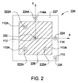
図2を参照すると、図2は本発明の一実施形態に従ってモニタし終点を検出するフォトマスク基板220の位置の一部の概略図である。基板220の中央領域225はリソグラフィを目的としてパターン形成されるフォトマスク区域として規定され、周辺領域とはパターン形成された中央領域の外側であり、これらの領域は終点又はその他の処理パラメータの監視に利用されるパターン又は特徴部を含む。基板支持部材16に配置された幾つかの窓部が仮想線で図示されている。例えば、フォトマスク基板220が基板支持部材16の中央に配置される場合、窓部112を通して光学的にアクセスすることでフォトマスク220の中心付近の監視が可能となり、フォトマスク220の周辺領域227の領域224、226は窓部114、110を通してそれぞれ監視可能である。一実施形態において、監視した領域224、226はフォトマスク220の一辺沿い、及び角部にそれぞれ位置される。別の実施形態において、監視領域224はフォトマスク220の一辺、例えばフォトマスク220の中心に対してX軸方向の辺の中点に位置し、その一方で例えばフォトマスク220の中心に対してY軸方向の、フォトマスク220の隣接する辺に位置している別の領域224Aは別の窓部114Aを通して監視される。112、114及び114A等の窓部を通して得られた光信号を用いてX及びY軸方向に沿った、或いはより一般的には互いに直交した方向に沿った中心から縁部に向かってのエッチング均一性を得ることが可能である。
Referring to FIG. 2, FIG. 2 is a schematic diagram of a portion of the position of the
1つ以上の窓部112Aを基板支持部材16に設けることでフォトマスク220の中央領域225の222A等の異なる領域の監視が可能になる。窓部112A、114Aを追加することで縁部から中心に向かってのエッチングプロファイルの測定が円滑になる。例えば、縁部から中心にかけてのエッチングプロファイル等の処理均一性に関する情報はフォトマスク220の異なる領域又は位置での終点結果を例えば領域222、224及び224Aからの信号に基づいて比較することで得ることができる。また、窓部を用いて窓部112、122Aの少なくとも1つがエッチング中の特徴部の下にあることを確認することができる。
By providing one or
図1Aを再度参照すると、終点検出システム164は反射又は透過モードで作動させるための光学装備を備え、反射率、透過率、干渉法、又は発光分光法の各種測定用に構成される。例えば処理中の材料層又は基板構造といった対象となる用途に応じ、反射率又は透過率強度における変化、干渉縞の数、又は特定の波長での発光強度における変化、又はその組合せに基づいて終点を検出する。
Referring again to FIG. 1A, the
反射モードで運転することにより、反射率(又は反射率測定)及び干渉計測を行うことができる。終点システム164は、通常、光源166、光源166からの入射光ビーム176を基板220の背面の領域又は点180に集束させるための集束アセンブリ166と、基板220の領域180で反射した戻り光ビーム178の強度を測定するための光検出装置170を備える。光検出装置は、通常、単一波長又は多波長検出装置又は分光装置である。反射光ビーム178の測定信号に基づき、コンピュータ172は実時間波形の一部を算出し、それを保存されている特性波形と比較し、エッチング処理に関連する情報を抽出する。この場合、計算は例えば膜が完全にエッチングされた際の、反射又は透過モードのいずれかにおける、検出信号の勾配変化又はその他の特性変化に基づいて行う。或いは、エッチング中のトレンチの深さ又は膜厚の変化に伴う干渉信号に基づいて計算する。その他の実施形態においては、広いスペクトルに亘って得られた反射及び透過データに基づいてより詳細な計算を行うことで、エッチング処理のいずれの時点での深さ又は厚さを求める、又はエッチング中の特徴部の横寸法を求める。
By operating in the reflection mode, reflectance (or reflectance measurement) and interference measurement can be performed. The
光源166は単色、多色、白色光、又はその他の適した光源である。通常、反射ビーム178からの光信号を分析して層(例えば、金属含有層)の有無、又は領域180内の特定の材料層の厚さに関しての情報を抽出する。入射光ビーム176の強度は測定可能な強度の戻りビーム178を得るに十分な強さとなるように選択される。一実施形態において、光源166は例えば波長範囲約200nm〜約800nm、又は約400〜800nmの光をそれぞれ発生するHg−Cdランプ又は発光ダイオード(LED)から多色光を発する。多色光源166にフィルタを取り付けることで選択した周波数を有する入射光ビーム176を得ることが可能である。カラーフィルタを光検出装置170の前面に配置することで、光検出装置170に進入する戻り光ビーム178の強度を測定する前に、所望の波長の光を除く全ての波長を排除可能である。光を分光装置(波長分散素子を備えたアレイ検出器)により分析することで紫外線から可視光といった約200nm〜800nmの広い波長範囲に亘ってデータを得ることが可能である。光源は連続又はパルスモードで動作するよう構成することができる。連続検出の場合、プラズマ発光のものより高い出力強度の光源を用いるのが好ましい。多波長出力の光源の場合、その強度がプラズマからの対応する波長の強度より高いものを選択可能である。パルスモード運転の場合、検出装置が光源とプラズマからの強度で飽和しない限り、光源強度についてのこういった要件は緩やかである。
The
パルスモード運転の場合、光源には多様な選択肢がある。例えば、光源166は安定した又は連続的な放射光出力をするいずれの適切な光源であってもよい。シャッタ(図示せず)を設置することで光源166からの出力ビームを遮断、開放し、信号検出用に交互のビームオン/オフサイクルとすることが可能である。ビーム「オン」期間中に捕捉した信号はプラズマ発光からの寄与分と光源166により誘導されたものを含み、ビーム「オフ」期間に捕捉した信号はプラズマ発光に対応する。ビーム「オフ」信号をビーム「オン」信号から減算することで測定が向上し、これはプラズマ発光からの干渉の可能性が排除されるからである。こういったデータ減算ルーチンは終点検出システムに関連したアルゴリズムの一部として設けることが可能である。
For pulse mode operation, there are various options for the light source. For example, the
パルスモード運転は、例えば図7に図示されるように、光源166をそのスイッチが交互サイクルでオン、オフとなるように構成することで達成することもできる。図7の実施形態において、レチクル700はエッチングチャンバ内のプラズマ702下方に位置されている。終点検出システム704はレチクル700の底部とインターフェース接続するように位置される。終点検出システム704は光ファイバ束706を含み、光ファイバ束の一端は基板支持体(図示せず)に形成された1つ以上の窓部を通してレチクル700の底部が観察できるように位置されている。光ファイバ束706は光源166で生成され、レチクル700で反射された信号を検出装置170に伝達する。概して、光源の遮断又は切り替えは様々なデューティサイクルと信号捕捉時間の組合せで行うことができ、例えば、バックグランド減算するために光源デューティサイクルを検出装置のデューティサイクルと整合するよう選択する。また、光源強度を調節して電荷結合素子(CCD)又はその他の適切な装置等の検出装置170の飽和を回避することができる。パルス幅が検出装置サンプリング時間よりも短い場合、ランプを複数回に亘りパルス点灯して集積により総強度を高くすることができる。一実施形態においては50パーセントのデューティサイクルを使用する。光源がオンの場合(つまりシャッタが開放されている)、検出装置によって感知された光にはランプとプラズマ双方からの光が含まれる。光源がオフ(つまりシャッタが閉鎖されている)場合、検出装置によって感知された光にはプラズマからの光のみが含まれる。信号における差異を用い、プラズマからの光のバックグラウンド寄与分を検出した信号から減算することで、より正確な終点表示を得られる。
Pulse mode operation can also be achieved, for example, by configuring the
或いは、異なるサンプリング時間を用いることでバックグラウンド減算を行ってもよい。例えば、検出装置、例えばCCDのサンプリング時間を光源「オン」時間中は短く維持し、続いて光源「オフ」時間中は長くすることができ、この間にバックグラウンドプラズマ発光を集光する。この方法は例えば透過方式監視における場合のように発光それ自体を二次信号として使用する場合に、バックグラウンドプラズマ発光におけるノイズの軽減に有用である。 Alternatively, background subtraction may be performed by using different sampling times. For example, the sampling time of a detection device, eg, a CCD, can be kept short during the light source “on” time, and subsequently increased during the light source “off” time, during which background plasma emission is collected. This method is useful for reducing noise in the background plasma emission, for example, when the emission itself is used as a secondary signal, as in transmission mode monitoring.
信号捕捉時間と光源「オン」時間の選択は具体的な用途と光源の強度に依存する。概して、比較的出力強度の低い光源の使用では信号捕捉時間を長くする必要がある。一実施形態において、ビーム「オン」時間は約0.1秒〜約2秒である。 The choice of signal acquisition time and light source “on” time depends on the specific application and light source intensity. In general, the use of a light source with a relatively low output intensity requires a longer signal acquisition time. In one embodiment, the beam “on” time is from about 0.1 seconds to about 2 seconds.
光源166は選択した波長で発光する単色光源、例えばHe−Ne又はND−YAGレーザ、又は発光ダイオード(LED)等の固体光源であってもよい。その他の選択肢には多波長で放射光出力する水素(H2)、重水素(D2)、グリムベルゲン(Grimbergen)による米国特許第6534756号で開示されるような蒸気ランプ、又は中空陰極ランプ等の多様な放電ランプが含まれる。一実施形態において、光源166は異なる波長領域で放射光出力をする多数のLEDを含む。例えば、光源166は以下に挙げるものの少なくとも1つを含む。紫外線(UV)領域のLED、赤外線(IR)領域のLED、広帯域(例えば、白色光)出力のLED、又はその組合せ。異なる出力波長、例えば370nm(UV)、390nm(UV)、400〜700nm(白色)、800nm(IR)、1300nm(IR)、1500nm(IR)のLEDの組合せを用いることで、UVからIR領域に亘るスペクトル出力、例えば約350nm〜約1500nmを達成可能である。この場合、光源166にはファイバが各LEDと結合している出力ファイバ束を取付け可能である。
The
再度図1Aに図示の実施形態に戻るが、1つ以上の凸面集光レンズ174a、174bを用いて入射光ビーム176を基板表面上の領域180へと集光し、戻り光ビーム178を光検出装置170の活性表面へと再度集光している。領域180は基板220の表面トポグラフィやデバイス設計フィーチャにおけるばらつきを補償するに十分な広さでなくてはならない。これにより例えばビア又は深くて狭いトレンチ等の口径の小さい開口部を有する、高密度又はもう少し間隔のあいた高アスペクト比特徴部のエッチング終点の検出が可能となる。戻り光ビームの領域は、光検出装置170の活性光検出表面の大部分を活性化するに十分に広くなくてはならない。入射及び戻り光ビーム176、178は光ビームの処理環境内外での往来を可能とするところの処理チャンバ10の透明窓部110を通して指向される。図1Aにおいてはレンズ172aと174bを窓部110から離して図示しているが、実際には図1Bに図示されるようにレンズを窓部110に近接して取り付けてもよい。また、当然ながら、入射及び戻り光ビーム176、178は通常、光ファイバを介して終点検出システム164に結合可能である。光ファイバを使用して光ビームを窓部内外で結合することにより、基板支持部材16と検出器エレクトロニクスとの間で絶縁が維持される。
Returning again to the embodiment shown in FIG. 1A, one or more convex condensing lenses 174a, 174b are used to condense the
ビームスポット180の直径は通常、約2mm〜約10mmである。しかしながら、ビームスポット180が、少数のエッチング特徴部しか有さない広い基板隔離領域を含む場合、より大きなビームスポットを使用してより多数のエッチング特徴部を網羅する必要のある場合がある。従って、ビームスポットのサイズは特定のデバイスの設計フィーチャに応じて最適化が可能である。信号が十分な場合は、広いビームスポット又は視野により、基板支持穴と信号を発生する基板エッチング領域とを正確に整合させることなく処理制御が可能となる。
The diameter of the
任意で、光ビームポジショナ184を用いて入射光ビーム176を基板220上で移動させ、ビームスポット180を位置させてエッチング処理を監視するところの基板表面の適切な部位を定めてもよい。光ビームポジショナ184は、小角度で回転して光源166からの光ビームを基板表面の異なる位置に偏向する1つ以上の一次ミラー186を含んでいてもよい。追加の二次ミラーを用いて(図示せず)、戻り光ビーム178を光検出装置170上に指向してもよい。光ビームポジショナ184も用いて基板220の背面全体を光ビームでラスター走査してもよい。この実施形態において、光ビームポジショナ184は可動ステージ(図示せず)から成る走査アセンブリを備え、このステージ上に光源166、集束アセンブリ168、及び検出装置170が取り付けられる。可動ステージをステッピングモータや検流計等の駆動機構により設定したインターバルで移動させ、基板220全体をビームスポット180で走査可能である。
Optionally, a
光検出装置170は光電池、フォトダイオード、又はフォトトランジスタ等の光感応性電子部品を備え、戻り光ビーム178の測定強度に応答して信号を生成する。信号は電子部品内を流れる電流レベルの変化として、或いは電子部品全体に印加された電圧における変化として表すことができる。また、光検出装置170は紫外線から可視光といった約200nm〜800nmの広波長範囲に亘ってデータを提供する分光装置(波長分散素子を備えたアレイ検出器)も備える場合がある。戻り光ビーム178は光ビームの強度を増大又は減少させる建設的干渉及び/又は相殺的干渉を受け、光検出装置170は反射した光ビーム178の測定強度に関連して電気的出力信号を供給する。電気的出力信号を時間の関数としてプロットすると、反射光ビーム178の様々な強度に対応した多数の波形パターンを有するスペクトルが得られる。コンピュータシステム172のコンピュータプログラムが反射光ビーム178の測定波形パターンの形状を保存されている特性(又は基準)波形と比較し、測定波形パターンが特性波形パターンと同一である場合、エッチング処理の終点を決定する。このため、干渉信号の期間を用いて深さとエッチング速度を計算することができる。また、プログラムを測定波形に用いて変曲点等の特性波形を検出してもよい。手順は、移動導関数を求めて変曲点を検出する等の簡単な数学的なものとなる。図1Aは終点システム164に接続したコンピュータシステム172を図示しているが、システムのその他の終点検出装置からのデータを処理するためにも用いられる。
The
図1Aは基板支持部材16における光アクセスポート又は窓部110及び112の相対位置を図示することを意図している。2つの代替光学構成の拡大断面図が図1Bに概略的に図示されている。基板支持部材16には凹部132、134が設けられており、開口部又はチャネル136、138に別々に接続され、基板220の背面への光学アクセスを可能としている。凹部132、134には窓部124、126に真空シールするためのOリングと溝142、144がそれぞれ設けられている。片方の構成は窓部124を通した反射方式測定に基づいた終点検出を図解したものであり、ファイバ121の入射光はレンズ123により基板220上に集束される。基板220の背面から戻った信号は次にレンズ123によりコリメートされ、ファイバ125を介して終点検出システム164に結合される。レンズ123には異なる焦点距離を用いてもよく、一実施形態において、使用する焦点距離は約15mmである。別の実施形態において、コリメートレンズ123は除外してもよく、この場合はファイバ121、125を窓部124に押し付けて取り付ける。具体的な測定及び光学構成に応じ、ファイバ121及び125は単一ファイバ又はファイバ束(1本以上のファイバを有する)のいずれかと称される。複数のファイバを使用することで、例えば信号強度の向上や異なる領域での同時サンプリングを含む新たな機能が加わる。
FIG. 1A is intended to illustrate the relative positions of the optical access ports or
もう一方の構成は窓部126を通した透過方式測定に基づく終点検出を表す。透過信号、例えばプラズマ発光又は外部光源は窓部126を通過して、ファイバ127により検出のために集光される。図1Bに図示されるように、開口部又はチャネル138には基板支持部材16の上面近くにテーパー又は円錐部140が設けられている。円錐部140の上部は内部、つまり凹部134に近い部位に比べて直径(又は横寸法)が大きい。このデザインには、窓部126のサイズを大きくすることなく基板220での視野又はサンプリング領域が広くなるという利点がある。一実施形態において、円錐部140は開口数約0.22を有するファイバとする場合、広がり角約25°の視野となるように形成される。視野はファイバ127と窓部126との間の距離を調節することによっても変更可能である。任意で、発散レンズも用いて放射光をファイバ127に結合してもよい。
The other configuration represents end point detection based on transmission measurement through the
当業者に既知の様々な取付部品を用いて、様々な光学部品を基板支持部材16の内部に取り付け、固定する。図1Bでは明瞭化のために省略している。基板支持部材16は導体、例えば陽極酸化アルミニウムから成るため、取付部品は非導体又は何らかの方法で基板支持部材16から絶縁されているかのいずれかである。開口部136、138、及び凹部132、134のサイズは具体的なデザイン及び/又は処理要件によって異なり、例えば、光ビームスポットサイズ、所望のサンプリング面積、RFバイアスへの最少影響度その他等の要因を考慮する。例えば、凹部132、134の直径は数ミリ(mm)から数センチ(cm)、開口部136、138の直径は約1センチまでである。一実施形態において、直径約7mmの開口部をビームスポットサイズ約2mmと組み合わせて使用する。その他の代替デザイン案には基板支持部材16へのRFバイアスに影響を与える可能性を最小限にするために、導電グリッド又は導電性透明コーティングを窓部上に設けることを含む。
Various optical components are mounted and secured inside the
終点検出システム164は基板表面のどの領域のパターンでも検出できるように構成可能である。具体的な終点検出技法に応じて、基板上のパターンはフォトマスク上のいずれの適切なデバイス特徴部である、或いは終点検出を円滑に進めるための特定の特徴部デザイン又は寸法を有するテストパターンである。例えば、こういったテストパターンは、単一又は異なるピッチ及び/又は線幅のライン/スペースパターンである。
The end
図1Cは開口部136、138、窓部124、126、基板支持部材16及び基板220の相対位置の一実施形態を示す概略上面図である。基板220の辺又は縁部220Eは基板支持部材16の縁部16Eを越えて延びる。図示されるように、基板220の周辺領域227と中央領域225との境界は破線で示される。開口部138は中央領域225で終点を監視するために使用される。開口部136は基板220の周辺領域227と中央領域225の双方を含む範囲をカバーするが、終点監視目的、例えばエッチング均一性についての情報その他を得るためにもまだ使用可能である。或いは、開口部136を通した終点監視が周辺領域227に施された特定のテストパターンからの信号に基づく場合、こういった終点監視は検出信号が開口部136の視野内の中央領域225の特徴部から生じ得る干渉の影響を実質的に受けていない限り効果的に実行可能することが可能である。概して、不要な干渉を回避するため、テストパターンは基板220の中央領域225の特徴部から十分に離れた位置に設けられる。一実施形態においては、1つ以上のテストパターンを基板220の縁部220Eから最高約10mmの距離に設け、開口部を基板支持部材16の対応する位置に設置して終点を監視する。
FIG. 1C is a schematic top view illustrating one embodiment of the relative positions of the
図3は周辺領域に様々な終点監視位置を備えた6インチ正方形基板の上面図である。一実施形態において、終点検出は基板周辺領域315又は角部325に配置された1つ以上のテストパターン330の監視に基づいて行われ、終点検出システム164は基板のこれらの領域の真下に配置される。例えば6インチ四方の基板の場合、終点検出システム164の窓部は、図3に図示されるように、基板220の水平中心線310から少なくとも約2.6インチ、例えば2.6〜2.9インチ離して、基板220の垂直中心線320から少なくとも約2.6インチ、例えば約2.6〜2.9インチ離して配置される。窓部112は通常、線310、320の交差部に位置される。基板の中央領域225内の領域を監視するために、窓部112Aは通常、基板支持部材16の面の中心から2.6インチ未満の場所に位置される。一実施形態において、テストパターンはビームスポットとほぼ同じ又はそれより大きいサイズを有する。
FIG. 3 is a top view of a 6 inch square substrate with various endpoint monitoring positions in the peripheral area. In one embodiment, endpoint detection is based on monitoring one or
同一パターンを有する各基板から反射した光ビームは、終点検出システム164で検出される際に同一波形パターンを有するように構成される。このため、同一テストパターンから得た波形パターンを用いてチャンバが特定のプロセスレシピに応じて作動しているか否か、及び基板ごとに所望のエッチング結果が得られたか否かを求めることができる。
The light beams reflected from the respective substrates having the same pattern are configured to have the same waveform pattern when detected by the end
周辺領域には様々な寸法及び/又はデザインのテストパターンを容易に設けることができる一方、こういったパターンのフォトマスク中央領域への配置にははるかに多くの制限がある。このため、中央領域での終点監視に使用可能な特徴部はデバイスのデザインとフォトマスク上でのレイアウトに依存する。例えば開放領域が不十分なために監視領域では監視に十分な強度の光信号が得られない場合、代替の光学構成を用いて視野を拡大する又は複数のサンプリング領域を設けることができる。こういった代替案にはより高い開口数(NA)を有する光学部品、例えばテーパー状端部を備えたファイバを含むレンズ及びファイバの使用、又は異なる領域のサンプリングを行うためのファイバ束の使用が含まれる。より高いNAの光学部品を使用することで、窓部のサイズを上げることなくサンプリング領域を拡大することができる。複数のファイバ(例えば、ファイバ束)の使用により、基板の別々の領域での光信号の監視が可能となる。具体的な特徴部及び検出法に応じ、基板の中央領域全体に亘る異なる位置等のこれらの異なる領域からの信号を合算してより良好な信号としたり、或いは異なる信号を互いに比較して最も良好なものを選択して終点検出に使用してもよい。実施形態の多くにおいて、集光光学部品は基板面に実質的に垂直な方向で光信号をサンプリングするよう構成されている。別の実施形態において、集光光学部品は斜め視野角から、つまり基板に対して非直角方向からも信号をサンプリングする。この斜め視野角構成によっても、同一の集光光学部品を用いた垂直構成と比較してサンプリング領域が拡大する。 While test patterns of various dimensions and / or designs can be easily provided in the peripheral area, there are much more restrictions on the placement of such patterns in the central area of the photomask. For this reason, features that can be used for endpoint monitoring in the central region depend on the device design and the layout on the photomask. For example, if an optical signal with sufficient intensity for monitoring cannot be obtained in the monitoring area due to insufficient open area, an alternative optical configuration can be used to expand the field of view or provide multiple sampling areas. These alternatives include the use of optical components with higher numerical aperture (NA), such as lenses and fibers, including fibers with tapered ends, or the use of fiber bundles to sample different areas. included. By using an optical component having a higher NA, the sampling area can be expanded without increasing the size of the window. The use of multiple fibers (eg, fiber bundles) allows optical signal monitoring in different areas of the substrate. Depending on the specific features and detection methods, signals from these different regions, such as different positions across the entire central region of the substrate, may be summed to make a better signal, or different signals may be compared to each other to best May be selected and used for end point detection. In many of the embodiments, the collection optics is configured to sample the optical signal in a direction substantially perpendicular to the substrate surface. In another embodiment, the collection optics also samples the signal from an oblique viewing angle, i.e., from a non-perpendicular direction with respect to the substrate. This oblique viewing angle configuration also enlarges the sampling area compared to a vertical configuration using the same condensing optical component.
透過モードで運転する場合、終点検出システム164は透過率(例えば、総光強度)又は発光信号(例えば、波長分解発光)を時間の関数として監視する。一実施形態において、チャンバ10内のプラズマは発光監視における光源として機能する。この構成には、反射モードと比較して光学設備が単純化されるという利点を有するが、これは外部光源を必要とせず、光ファイバを1つしか必要としないからである。
When operating in transmission mode,
プラズマ発光は、典型的には、プラズマに存在する多様な種に特徴的な離散した波長の光を含む。例えば、発光は1つ以上のエッチャント/反応物又はエッチング生成物種に対応する1つ以上の波長で監視することが可能である。エッチング終点、例えば特定の材料層が完全にエッチングされ、その下の層が露出した際、監視される発光強度は監視中の発光種に増減に応じて変化する。概して、終点検出システム164の発光検出装置150は集光アセンブリ152、波長分散素子156及び光検出装置158を備える。一実施形態において、集光アセンブリ152は光ファイバ153と、任意で光信号をファイバ153に結合するためのレンズ154を含む。波長分散素子156は光信号178をその成分波長に分離するための分光装置であってもよい。別の実施形態において、集光光学アセンブリ152はレンズ及び鏡等の多様なバルク光学部品を含み、波長分散素子156は特定の範囲の波長のみ透過させる各種フィルタである。配列によっては、光検出装置158は特定の波長で光信号を検出するように構成される、又は異なる波長の信号を同時に検出する。適切な光検出装置にはフォトダイオード、光電子増倍管又は電荷結合素子その他が含まれる。
Plasma emission typically includes discrete wavelengths of light characteristic of the various species present in the plasma. For example, the emission can be monitored at one or more wavelengths corresponding to one or more etchant / reactant or etch product species. When an etching end point, for example, a specific material layer is completely etched and the underlying layer is exposed, the monitored emission intensity changes according to the increase or decrease in the monitored emission species. In general, the
図1Aの実施形態は終点検出システム164の異なる光学部品に結合された窓部110、112からの異なる光信号、例えば反射及び透過信号を示すが、窓部110、112を通して監視された2つの信号は同一タイプの光信号、例えば双方共に反射率信号又は透過率信号等であってもよい。加えて、窓部110、112からの2つの光信号は同じ光検出装置に結合してもよい。例えば、撮像光検出装置を使用する場合、ある窓部からのプラズマ発光信号を検出装置の第1検出素子又は画素群上に画像化し、第2窓部からのもう一方の発光信号を同一検出装置の第2検出素子又は画素群上に画像化する。
The embodiment of FIG. 1A shows different optical signals from
更に、図1Aでは基板支持部材16には窓部110と112だけ配置して示し、その他の光学部品は基板支持部材16の外部に図示しているが、こういった描写は一部は説明のため、一部は図の明瞭化のためである。当然ながら、終点検出システム164の1つ以上の光学部品、例えば窓部、光ファイバ、レンズ、光検出装置その他を基板支持部材16内に配置又は埋設する、或いは光アクセス窓部110又は112と一体化させることもできる。別の組合せの各種光学測定及び信号検出構成もまた基板の2つ以上の位置での終点監視に有利に使用可能である。
Further, in FIG. 1A, only the
別の実施形態において、プラズマ源との併用又はプラズマ源の代わりに外部光源190を使用することで、透過率測定についての機能を拡張する、又は透過率測定を有利にすることができる。透過モードの場合、外部光源190を天井部13に設置された窓部192を通してチャンバ10内へと結合する。透過率測定のための外部光源190の使用はプラズマ源よりも有利であり、これは外部光源のほうがエッチング処理から生じる変動の影響を受ける可能性のあるプラズマ発光よりもより安定した信号を供給可能だからである。外部光源190はプラズマ種からの干渉の可能性のない選択波長での監視を可能とするよう構成される。光源166と同様に、外部光源190をパルスモードで運転し、例えばプラズマ発光から考えられ得る変動を減算することで、終点検出能力を向上させるための様々な信号処理選択肢が見込める。光源190を用いたパルス式光源動作についての詳細は、光源166について上述したものと同様である。その他の実施形態は、反射方式及び透過方式測定の双方についてパルス方式光源の使用を伴う。別の実施形態において、外部光源190は基板支持部材16の光アクセス窓部(図示せず)を通して供給され、透過信号は窓部192を通して監視される。反射率監視の例としては、光源190からの出力はファイバ194を介して結合され、窓部192を経由してフォトマスク等の基板220上へと通過する。(例えば、フォトマスク上の特徴部で反射した)反射光はコリメートレンズ196により集光され、広帯域分光検出装置198に繋がる別のファイバに結合される。分光装置198は光をその波長成分、例えば約200nm〜800nmへと分離し、第1スペクトルを記録する。
In another embodiment, the use of an external
第2スペクトルはパルス方式光源をオフにして収集する。これにより、次に第1スペクトルから減算可能なバックグラウンドスペクトルが得られる。差スペクトルは反射光のみからの寄与分を含み、プラズマ光による影響を受けない。この2つのスペクトル収集シーケンスはエッチング処理中、各データポイントごとに繰り返す。この結果、プラズマ発光が比較的強い場合に起こり得るプラズマにおけるいかなる変化も、測定した反射率には影響しない。 The second spectrum is collected with the pulsed light source off. As a result, a background spectrum that can be subtracted from the first spectrum is obtained. The difference spectrum includes the contribution from the reflected light only and is not affected by the plasma light. These two spectral acquisition sequences are repeated for each data point during the etching process. As a result, any changes in the plasma that can occur when the plasma emission is relatively strong do not affect the measured reflectivity.
基板(フォトマスク)は誘電性、例えば透明であるため、バックグラウンド減算を伴う反射方式測定設備は基板220のどちらの側からでも設置可能である。つまり、ファイバ束及びコリメート光学部品を天井部13に取り付けて、基板220からの信号を天井窓部192を通して収集可能する、又はファイバ束を基板220の下方に位置させて基板の背面から監視することが可能である。
Since the substrate (photomask) is dielectric, eg, transparent, a reflective measurement facility with background subtraction can be installed from either side of the
下方(つまり基板を介した)からの終点監視である後者の構成には少なくとも2つの利点がある。第1に、Cr等の吸収層のエッチングの場合、基板背面からの光信号は、基板下方からの監視は基板上面上方からの監視に比べて、フォトレジストマスク層の厚みにおける変化の影響をあまり受けない。第2に、用途によっては、光学サンプリング領域は狭いほうが望ましい。例えば、石英エッチングの場合、均一なパターンを有する指定のテスト領域内で測定した際に、干渉法は最も正確となる。従って、コリメート光学部品が基板に近接している背面監視の採用により、チャンバの天井部からのものよりも小口径の光ビームが使用可能となる。 The latter configuration, which is endpoint monitoring from below (ie through the substrate), has at least two advantages. First, in the case of etching of an absorption layer such as Cr, the optical signal from the back surface of the substrate is less affected by the change in the thickness of the photoresist mask layer when monitored from below the substrate than when monitored from above the top surface of the substrate. I do not receive it. Second, depending on the application, it is desirable that the optical sampling area be narrow. For example, in the case of quartz etching, interferometry is most accurate when measured within a designated test area having a uniform pattern. Thus, by employing backside monitoring where the collimating optical component is close to the substrate, a light beam having a smaller aperture than that from the ceiling of the chamber can be used.
この減算技法は透過方式測定にも応用可能であり、光源及び検出装置は処理する基板の両側に配置される。これは天井部の窓部、基板保持体の窓部、及び集光のための別の光学部品を必要とする。 This subtraction technique can also be applied to transmission-type measurements, where the light source and detector are located on both sides of the substrate being processed. This requires a window portion on the ceiling, a window portion on the substrate holder, and another optical component for light collection.
図4A−Cは種々の終点検出技法で監視し得るフォトマスク基板の製作中の様々な構造を図示する。図4Aは金属含有層414、例えば酸化クロム及びクロムを含み、ガラス又は石英層412上に配置されたクロム層をエッチングするための、パターン形成したフォトレジスト416を備えた二層フォトマスク構造410を示す。クロム層414のエッチングについての終点は反射又は透過モードのどちらでも監視可能であり、反射率、透過率及び/又は発光測定を実行可能である。
4A-C illustrate various structures during the fabrication of a photomask substrate that can be monitored with various endpoint detection techniques. FIG. 4A shows a two-
例えば、終点検出システム164からの入射光ビーム402を基板支持部材の窓部の1つを通してフォトマスク基板410の一領域へと指向する。入射ビーム402とフォトマスク構造410との相互作用、例えばクロム層414の裏面での反射(又はクロム層と石英層との界面)から生じる戻りビーム404は終点検出システム164の光検出装置170により検出される。クロム層414のエッチング終点で、反射率信号は減少し、これはフォトマスクの開放領域415(フォトレジストがない領域)におけるクロム層が除去され、破線405で図示されるように、これらの領域からの反射ビームが喪失するからである。更に、反射スペクトルの回折解析を行ってクロム特徴部のエッチングプロファイルを推定し、クロム特徴部の基部が除去された際にエッチング処理を終了することができる。こういった分析により、特徴部のエッチングプロファイルの制御が可能となる。
For example, the
透過モードの場合、例えばプラズマからの開放領域415を通過する発光信号を監視する。一実施形態においては、発光の総強度、つまり透過率を測定する。別の実施形態においては、発光を波長分散素子に結合し、信号を1つ以上の選択した波長で監視する。クロム残分厚さが比較的小さいクロムエッチングの終了を前にして、クロム厚さも透過信号から推定可能である。
In the case of the transmission mode, for example, the emission signal passing through the
図4Bは減衰位相シフトマスクの製作中における、別のフォトマスク構造420を示す。構造420は石英層422上に形成された位相シフト材料層428、例えばケイ化モリブデン(MoSi)を有する。クロム層424はMoSi層428上に堆積され、続いてフォトレジスト層426が堆積される。フォトレジスト層426にパターン形成し、クロム層424のためのエッチングマスクとして使用する。次にケイ化モリブデン(MoSi)層をマスクとしてのパターン形成したフォトレジスト層426、又はハードマスクとしての(フォトレジスト層426を剥離した後)パターン形成したクロム層424のいずれかを用いてエッチング可能である。クロムエッチングと同様に、MoSiエッチングの終点は反射又は透過モードのいずれかでも監視可能であり、反射率、透過率、又は発光測定を実行可能である。MoSiは部分透過性であることから、終点監視には干渉計測も使用可能である。
FIG. 4B shows another
図4Cは石英位相シフトマスク製作用の別のマスク構造430を示し、パターン形成したクロム層434がその下の石英層432をエッチングするためのハードマスクとして機能している。本来の、つまりエッチング前の石英基板432の上面436が図4Cにおいては破線で描かれている。この場合、石英層432を本来の表面436下方の特定の既定深さd1までエッチングしなくてはならない。反射モードで終点検出システム164を動作させることで、特定の波長の戻りビーム178を時間の関数として監視し、干渉データ、例えば異なる厚みの材料層を通過する反射ビーム178の異なる部分間での光学干渉から生じる干渉縞の出現を得る。例えば、入射光ビームの一部402Aはフォトマスク430の開放領域で反射し、入射光ビームの別の部分402Bはフォトマスク430のマスク領域、例えばクロム層/特徴部434を有する領域で反射される。2つの反射部分405A及び405B間の干渉により干渉縞(つまり、強度変調)が生成され、干渉縞はこれらの部分405A、405Bが横断する石英層の厚みにおける違いを示している。反射ビームの干渉縞を監視することにより、エッチング深さd1を求めることができる。一実施形態において、干渉法式終点監視は図1Aの光源166に関連して上述したようにパルスモードで行う。概して、干渉法式監視には狭帯域光源が適している。従って、プラズマ発光がこの目的に十分な狭帯域を有している限り、干渉法式監視にプラズマを光源として使用することが可能である。
FIG. 4C shows another
図5は終点検出システムを用いた、Crマスクのエッチング中に時間の関数として同時に監視された3つの光信号を表す。クロム層はプラズマ含有塩素及び酸素ガスを用いてエッチングする。一番上のトレース510はCrからの発光信号を監視する、例えばCrからの、例えば波長520nmの原子線を直接的に監視する、或いはCr輝線及び塩素輝線(例えば、258nm)を監視し、Cr:Cl発光信号の比をとることのいずれかで得られる。典型的には信号対雑音比はエッチング生成物の発光信号と反応物の比(又はその逆)をとることで改善可能である。クロムエッチングが終点に近づくにつれ、プラズマにおけるクロム含有種(エッチング生成物)の濃度は低化し、一番上のトレース510のポイント512で示されるように、それに対応してCr発光信号(又はCr:Cl発光比)が変化する。概して、発光信号はチャンバ10の、例えば基板支持部材16又は天井部に設けられた1つ以上の窓部を介して、プラズマを直接見ることで監視可能である。加えて、図1Aに図示されるように、側部窓部193をチャンバ壁部に設け、例えば発光を発光検出システム195に結合することで、プラズマ発光を検出することができる。発光分の発光検出システム195への結合によりプラズマ発光を検出するために、図1Aに図示するように、チャンバ壁部に側部窓部193を設置してもよい。側部窓部193を通しての発光監視は1つ以上のその他の窓部を介した終点監視と共に行ってもよい。
FIG. 5 represents three optical signals simultaneously monitored as a function of time during the etching of the Cr mask using the endpoint detection system. The chromium layer is etched using plasma-containing chlorine and oxygen gas. The
中央のトレース520はクロム層の底面で反射した光からの反射信号を監視することで得られ、図4Aに図示のものに類似している。クロムエッチングが終点に近づくにつれ、マスクの開放領域415におけるクロム層はクロムがエッチングにより除去されるにつれ薄くなり、部位514に図示されるように、監視された反射信号強度が低下する。
The
一番下のトレース530は透過率を監視することで得られる。部位516に示されるように、透過率信号強度はマスクの開放領域415のクロム層が除去された終点に近づくにつれ上昇し、これらの開放領域においては発光が石英層を透過可能となる。
The
これらの光学測定法を基板の2つ以上の位置での監視と組み合わせることで終点検出が強化され、処理制御が向上する。一実施形態において、終点検出システムは反射及び透過モードの双方で動作するように構成される。例えば、図1Aを再度参照すると、透過信号(例えば、透過率信号又はプラズマ発光信号)を窓部112を介して検出し、基板の中央領域の一範囲を監視し、反射信号(例えば、反射率信号又は干渉信号)を窓部110を介して検出して基板の周辺領域の一範囲を監視する。透過モードでの基板中央領域の監視は、反射モードと比較するとエッチング特徴部とアクセス窓部との間の整列要件が低めであり、更により広範囲を監視可能という点で有利である。
Combining these optical measurement methods with monitoring at two or more positions on the substrate enhances endpoint detection and improves process control. In one embodiment, the endpoint detection system is configured to operate in both reflective and transmissive modes. For example, referring again to FIG. 1A, a transmission signal (eg, a transmittance signal or plasma emission signal) is detected through the
従って、本発明の一実施形態は本発明の装置を用いて実行可能な方法を提供する。一実施形態において、本発明の装置は指示が記録されたコンピュータ可読性媒体を含み、この指示はコンピュータ172又はエッチング反応装置を制御するのに適した当該分野で慣用のその他のプロセッサ等により実行した場合に図6に図示されたもの等の方法をエッチングチャンバに実行させる。コンピュータ可読媒体はコンピュータ172のメモリに保存することも考えられ、サポート回路とプロセッサも含む。方法600は工程602から開始され、エッチングチャンバに第1窓部と第2窓部をそれぞれその中央領域と周辺領域に有する基板支持部材を設置する。工程604ではフォトマスクを支持部材上に載置し、工程606で処理ガスをチャンバ内に導入する。フォトマスク構造上に見られる異なる材料をエッチングするためには、典型的にはハロゲン含有ガスを使用する。例えば、塩素含有処理ガスを用いてクロム層をエッチングし、石英をエッチングする際にはトリフルオロメタン(CHF3)又はテトラフルオロメタン(CF4)等のフッ素含有ガスを用いる。工程608でプラズマを処理ガスから発生させ、工程610で第1及び第2光信号をそれぞれ第1及び第2窓部を通して検出する。工程612で、2つの検出光信号の少なくとも1つから得られた情報に基づいてチャンバ内のプラズマを終了する。更に、中心から縁部にかけての均一性等のエッチングプロファイル結果に基づき、エッチャントガス組成、流量、コイルバイアスその他の処理パラメータを調節して処理を最適化することができる。
Accordingly, one embodiment of the present invention provides a method that can be performed using the apparatus of the present invention. In one embodiment, the apparatus of the present invention includes a computer readable medium having instructions recorded thereon, when the instructions are executed by a
1つ以上の光学測定技法を適用して基板の異なる位置での同時監視を行うことで、本発明の実施形態は強化された処理監視と制御性能を備えた改善された装置と方法を提供する。こういった改良により低開放領域のフォトマスクエッチング用途についても信頼性の高い終点検出が可能となる。例えば、発光終点検出をクロム約3%、ケイ化モリブデン約1%の開放領域を有するフォトマスクのエッチングについて実施し、反射率測定を位相シフトマスク用途に向けて低開放領域クロムと石英のエッチングについて実施した。中心から縁部にかけてのエッチング均一性についての情報を提供することとは別に、異なるパターン密度の領域から生じるエッチング速度の変動も、本発明の終点検出システムを用いて複数の光信号を監視することで得られる。例えば、フォトマスクの周辺領域の異なる領域に別々の特徴部サイズ又はパターン密度のテストパターンを設け、監視した光信号を用いて目的とするパターン密度についての適切なエッチング終点を算定又は求めることができる。 By applying one or more optical measurement techniques for simultaneous monitoring at different locations on a substrate, embodiments of the present invention provide improved apparatus and methods with enhanced process monitoring and control performance. . Such improvements enable highly reliable end point detection even for photomask etching applications in low open areas. For example, the detection of the light emission end point is performed for etching of a photomask having an open region of about 3% chromium and about 1% of molybdenum silicide, and the reflectance measurement is performed for etching of a low open region chromium and quartz for a phase shift mask application. Carried out. Apart from providing information about etch uniformity from center to edge, etch rate variations resulting from regions with different pattern densities can also be monitored using the endpoint detection system of the present invention for multiple optical signals. It is obtained by. For example, it is possible to provide test patterns having different feature sizes or pattern densities in different regions around the photomask, and calculate or obtain an appropriate etching end point for the target pattern density using the monitored optical signal. .
基板支持体において単一の窓部を利用することで基板を監視することも想定される。特には、上述の特徴を単一の窓部と共に利用して、単一窓型終点検出装置を有する慣用のシステムよりも基板監視性能を強化したものとしてもよい。 It is also envisaged to monitor the substrate by utilizing a single window in the substrate support. In particular, the above features may be used with a single window to enhance the board monitoring performance over conventional systems having a single window endpoint detector.
本発明の別の実施形態において、エッチング処理監視システムにはプラズマを直接見るための手段(例えば、側部窓部)及びカソードの1つ以上の位置で加工対象物のエッチングを直視する手段(例えば、フォトマスク又はウェハ下のカソード窓部)が設けられている。これらの信号を様々に組合せて処理制御に使用することができる。一実施態において、エッチング処理監視システムは3個又は4個の窓部を備え、その内2個又は3個の窓部がエッチング範囲の周辺領域内にあるカソードと、1つは側部OES(発光分光)でもう片方は(フォトマスクを介した)「底部」である2経路の情報を同時に収集するように構成されたCCD終点システムを含む。「底部」光ファイバケーブルはカソードの3個又は4個の窓部のいずれの下にも配置可能である。典型的にはこの取付けは静的であり、光ファイバケーブルは中央又は縁部位置の1つのいずれかに固定される。底部光ファイバケーブルはバイアスRFエネルギーを終点システムに伝達することのないように電気的に絶縁状態で維持される。 In another embodiment of the present invention, the etching process monitoring system includes means for directly viewing the plasma (eg, side windows) and means for directly viewing the etching of the workpiece at one or more locations on the cathode (eg, , A photomask or a cathode window portion under the wafer). Various combinations of these signals can be used for process control. In one embodiment, the etching process monitoring system comprises three or four windows, two or three of which are in the peripheral region of the etching area, and one side OES ( The other in emission spectroscopy includes a CCD endpoint system that is configured to simultaneously collect information on two paths that are “bottom” (via a photomask). A “bottom” fiber optic cable can be placed under any of the three or four windows of the cathode. Typically, this attachment is static and the fiber optic cable is secured to either the center or edge position. The bottom fiber optic cable is maintained in an electrically isolated state so that it does not transmit bias RF energy to the endpoint system.
側部OES信号はマスクの広い範囲から生じ、底部信号は光学構成により決定されたマスク下の局部から生じる。典型的にはこの領域は約2〜5mmであるが、デザインによって変更可能である。 The side OES signal originates from a large area of the mask and the bottom signal originates from a local area under the mask determined by the optical configuration. This area is typically about 2-5 mm, but can vary depending on the design.
底部信号は反射方式(光源を使用。干渉法式終点(interferometric endpoint: IEP))又は透過方式(光源としてプラズマを使用。透過方式終点(transmission endpoint: TEP))と称される)である。光源及び関係する光ファイバケーブルを使用してもよいが、代替として、プラズマによる光を利用する透過モード(TEP)を用いてもよく、信号はフォトマスクを通して検出される。 The bottom signal is a reflection type (using a light source, interferometric endpoint: IEP) or a transmission type (using plasma as a light source, called transmission endpoint: TEP). A light source and associated fiber optic cable may be used, but alternatively, a transmission mode (TEP) utilizing light from plasma may be used, and the signal is detected through a photomask.
実施例及び利点には以下が含まれる。
1.より高い信頼性のための、特には低開放領域エッチング用途のためのOES終点及び底部終点の双方への到達の確認。例えば、終点検出方法の1つにおいて、OES及び底部終点を用いてプロセスドリフト及び/又は不正確さを検出する。
2.TEP中心及びOES(平均)について終点時間を比較することで処理均一性を評価及び監視し、エッチング条件を中央部高速型又は中央部低速型とする。
3.同様に縁部又は角部終点時間をOESと比較して左から右方向又は上部から底部に向かってのエッチング速度パターン差異を求める。
4.マスクを通したTEP信号をOES信号で割ることにより、TEP信号を正規化する。
4a.この正規化により真の透過測定値が得られ、プラズマ輝度と変動とは概して無関係となる。
4b.また、正規化により測定したマスクの分光透過率と透過についての実時間モデルとの比較が可能となり、エッチング中のエッチング層厚さ(例えば、Cr層)が求められる。
4c.また、正規化によりマスクの測定分光透過率と透過についての実時間モデルとの比較が可能となり、エッチング中のマスク層厚さ(例えば、フォトレジスト)が求められる。
4d.Crエッチング速度(4b)をPRエッチング速度(4a)で割ることにより、エッチング選択性が求められる。
Examples and advantages include the following.
1. Confirmation of reaching both OES endpoint and bottom endpoint for higher reliability, especially for low open area etch applications. For example, in one endpoint detection method, OES and bottom endpoint are used to detect process drift and / or inaccuracies.
2. The processing uniformity is evaluated and monitored by comparing the end point times for the TEP center and OES (average), and the etching condition is set to the central high-speed type or the central low-speed type.
3. Similarly, the edge or corner end time is compared with OES to determine the etching rate pattern difference from the left to the right or from the top to the bottom.
4). The TEP signal is normalized by dividing the TEP signal through the mask by the OES signal.
4a. This normalization provides a true transmission measurement and is generally independent of plasma brightness and variation.
4b. In addition, the spectral transmittance of the mask measured by normalization can be compared with a real-time model for transmission, and the etching layer thickness (for example, Cr layer) during etching is obtained.
4c. Also, normalization allows comparison of the measured spectral transmittance of the mask with a real time model for transmission, and the mask layer thickness (eg, photoresist) during etching is determined.
4d. Etching selectivity is determined by dividing the Cr etching rate (4b) by the PR etching rate (4a).
上述した透過方式及び/又は反射方式実施形態の全ては直視OES信号との比較に関連してここでも利用可能であることに留意しなくてはならない。また、ここで記載の実施形態はフォトマスク堆積用途、MEMSウェハ貫通エッチングの終点監視、シリコンウェハの堆積又はエッチングのいずれかの赤外線監視/処理制御、及び赤外線バンド端ウェハ温度測定に有用であることに留意しなくてはならない。 It should be noted that all of the transmissive and / or reflective embodiments described above can also be used here in connection with a comparison with a direct view OES signal. Also, the embodiments described herein are useful for photomask deposition applications, MEMS wafer through-etch etching end point monitoring, infrared monitoring / processing control of either silicon wafer deposition or etching, and infrared band edge wafer temperature measurement. You must keep in mind.
別の実施形態において、改善されたエッチング処理制御はエッチング中のフォトマスク上の膜の実時間透過率を監視することで円滑になる。吸収層(例えば、Cr)はエッチング開始時には小さいが計測可能な透過率を有し(典型的には1%〜15%。膜のタイプに依存する)、透過率は、膜がエッチング中に薄くなっていきエッチング終点で完全に(100%透過率)に除去されるまで予測可能な形で上昇する。単一光ファイバ束をフォトマスク下の窓部下に配置し、増大するプラズマ光を集光する。典型的には、観察領域は約2〜5mmであり、デザインを変えることで変更可能である。この構成は「透過方式終点(TEP)」と称することができる。 In another embodiment, improved etch process control is facilitated by monitoring the real-time transmittance of the film on the photomask being etched. The absorber layer (eg, Cr) has a small but measurable transmittance at the beginning of etching (typically 1% to 15%, depending on the type of film), and the transmittance is thin while the film is being etched. It rises in a predictable manner until it is completely removed (100% transmittance) at the etching end point. A single optical fiber bundle is placed under the window under the photomask to collect increasing plasma light. Typically, the observation area is about 2-5 mm and can be changed by changing the design. This configuration can be referred to as “transmission end point (TEP)”.
TEPの利点には、エッチング中の吸収膜の実際の光学的クリアリングに基づいた終点が含まれる。窓部の位置がエッチング中の膜のある領域の下であるとした場合、終点の信頼性は特には低開放領域エッチング用途の場合、OESよりも高くなる。終点システムはプラズマを光源として利用可能であり、外部光源の必要性がなくなる。光源がプラズマの場合、広い視野を使用可能であり、これによりカソードの開口部のサイズが最小化される。実施形態は光ファイバをカソード窓部近辺に設置するという、その他の光学部品を必要としない簡単なものとなる。 The advantages of TEP include endpoints based on the actual optical clearing of the absorbing film during etching. If the window location is below an area of the film being etched, the endpoint reliability is higher than OES, especially for low open area etching applications. The endpoint system can use plasma as a light source, eliminating the need for an external light source. If the light source is a plasma, a wide field of view can be used, which minimizes the size of the cathode opening. In the embodiment, an optical fiber is installed in the vicinity of the cathode window portion, and no other optical components are required.
TEPはクロム及びその他のエッチング用途で有利に使用することができる。こういった用途ではエッチングの経過に伴うクロム層を通過するプラズマ光の増大を検出するための、フォトマスク下に位置させた光ファイバを含む。一変化はTEP信号よりも若干小さいが、光源も用いて反射を監視してもよく、このため、TEPによりクロム用途の間、より高い分解能が得られる。 TEP can be advantageously used in chromium and other etching applications. Such applications include an optical fiber positioned under the photomask for detecting an increase in plasma light passing through the chromium layer as the etching progresses. Although the change is slightly smaller than the TEP signal, the light source may also be used to monitor reflections, so that TEP provides higher resolution during chrome applications.
TEPは石英エッチング用途にも使用することができる。こういった用途においては光干渉法を使用する。透過方式干渉法を用いてエッチング速度及び終点を監視可能である。プラズマを光源として用いるため、ランプを必要としない。終点透過率は、上述したように、TEP信号をチャンバ内に形成された側部窓部を通して得たOES信号で割り、プラズマ変化により生じた信号エンハンスを低減することで正規化することができる。プラズマが安定した光源となるに十分なほど安定している用途においては、バックグランド減算は不要である。また、反射方式干渉法を光源を必要とするコートエッチングに利用してもよい。光源は例えばUV領域の又はプラズマバックグラウンドより明るい安定したランプである。こういった適切な光源の例には重水素ランプ、高輝度放電ランプ(HID)、アーク灯、及び固体UV LED ランプが含まれる。また、光源のスイッチをオン・オフと切り替えることで、プラズマバックグランドからの信号の寄与分を信号から減算し、終点を示すより正確な信号が得られる。 TEP can also be used for quartz etching applications. In such applications, optical interferometry is used. Etching rate and endpoint can be monitored using transmission interferometry. Since plasma is used as a light source, no lamp is required. As described above, the end point transmittance can be normalized by dividing the TEP signal by the OES signal obtained through the side window formed in the chamber and reducing the signal enhancement caused by the plasma change. In applications where the plasma is stable enough to be a stable light source, background subtraction is not necessary. Further, the reflection type interferometry may be used for coat etching that requires a light source. The light source is a stable lamp, for example in the UV region or brighter than the plasma background. Examples of such suitable light sources include deuterium lamps, high intensity discharge lamps (HID), arc lamps, and solid state UV LED lamps. Further, by switching the light source on and off, the contribution of the signal from the plasma background is subtracted from the signal, and a more accurate signal indicating the end point can be obtained.
加えて、更に広いフォトマスク範囲をサンプリング可能である。ランプ構成に関し、コリメート光学部品を使用することができる。プラズマが光源の場合、カソードの単純な円錐視野を用いても、又は発散レンズを追加してもよい。どちらのランプ構成の場合も、走査型検出装置も使用することができる。カソードの光学窓部が大きい場合、金属グリッドを窓部を覆って取り付けてもよく、或いは透明導電膜(例えば、ITO又はZnO)を使用して基板の処理に必要なRFバイアスを維持可能である。 In addition, a wider photomask range can be sampled. For the lamp configuration, collimating optics can be used. If the plasma is a light source, a simple conical field of view of the cathode may be used, or a diverging lens may be added. In either lamp configuration, a scanning detector can also be used. If the cathode optical window is large, a metal grid may be mounted over the window, or a transparent conductive film (eg, ITO or ZnO) can be used to maintain the RF bias required for substrate processing. .
一実施形態において、例示的な検出装置を図8に示す。検出装置はフィルタ又はモノクロメータを備えたフォトダイオードPMT等の単波長検出装置である。基板支持体の各窓部は光ファイバケーブルで分離した検出装置に結合されている。検出装置は分光装置等の多波長検出装置であってもよい。分光装置は光ファイバ束の各部を独立した分光装置として画像化するものであってもよい。1つ以上の分光装置を用いて異なる位置からの複数のデータ同時収集を行ってもよい。 In one embodiment, an exemplary detection device is shown in FIG. The detection device is a single wavelength detection device such as a photodiode PMT provided with a filter or a monochromator. Each window portion of the substrate support is coupled to a detection device separated by an optical fiber cable. The detection device may be a multi-wavelength detection device such as a spectroscopic device. The spectroscopic device may image each part of the optical fiber bundle as an independent spectroscopic device. Multiple data collection from different positions may be performed using one or more spectroscopic devices.
図8に図示の例示的な実施形態において、光検出装置800は光ファイバ束802によりレチクル(図示せず)下の基板支持体に位置された複数の窓部804とインターフェース接続して図示されている。各窓部804からの信号(反射信号及び/又は透過信号)はポート806を介して光検出装置800に送られる。光検出装置800の信号は分光装置808と相互作用するに先立って、グレーティング又はプリズム等の波長分散素子810と相互作用する。各光ファイバ束802からの信号を単一の分光器808に伝達してもよく、又は各窓部804からの信号を別々に分析してもよく、信号を単一の分光装置に連続的に供給することで、又は各信号を別々の分光装置に供給することで行われる。
In the exemplary embodiment illustrated in FIG. 8,
具体的な実施には3個又は4個の窓部を備え、その内の2個又は3個の窓部がエッチング範囲の周辺領域にあり、1つが中央部にあるカソードと、1つは側部OES(発光分光)、もう1つは(マスクを介した)「底部」からの2経路の情報を同時に収集するように構成されたCCD終点検出システムが含まれる。「底部」光ファイバケーブルはカソードの3個又は4個の窓部のどの窓部下にも設置可能である。この取り付けは静的であり、光ファイバケーブルは中央又は縁部位置の1つに固定される。底部光ファイバケーブルはバイアスRFエネルギーを終点システムに伝達することのないように電気的に絶縁状態で維持される。これらの実施形態はフォトマスク堆積用途、その他の基板(例えば、ウェハ)のエッチング用途、MEMSウェハ貫通エッチング、シリコンウェハの堆積又はエッチングのいずれかの赤外線監視/処理制御、及び赤外線バンド端ウェハ温度測定に有用である。 Specific implementations have three or four windows, two or three of which are in the peripheral area of the etching area, one in the middle and one in the side Part OES (Emission Spectroscopy), the other includes a CCD endpoint detection system configured to collect two paths of information from the “bottom” (through the mask) simultaneously. A “bottom” fiber optic cable can be installed under any of the three or four windows of the cathode. This attachment is static and the fiber optic cable is fixed in one of the center or edge positions. The bottom fiber optic cable is maintained in an electrically isolated state so that it does not transmit bias RF energy to the endpoint system. These embodiments include photomask deposition applications, other substrate (eg, wafer) etching applications, MEMS wafer through-etching, infrared monitoring / processing control of either silicon wafer deposition or etching, and infrared band edge wafer temperature measurement. Useful for.
こういった構成の一例を図9−10に図示している。図9はフォトマスクレチクル902のエッチングに適したエッチング反応装置900の概略図である。エッチング反応装置900は基板支持体906を貫通して形成された窓部を介してレチクル902のエッチングを監視する終点検出システム904に結合されている。エッチング反応装置900の基板支持体906はRFプローブ908を介してRF発生装置910に結合されている。RFプローブ908はエッチング反応装置900内で行われるエッチング処理を能動的に制御する処理状態監視ソフトウェアを実装した制御装置912に結合されている。
An example of such a configuration is illustrated in FIGS. 9-10. FIG. 9 is a schematic view of an
基板支持体906は複数の窓部を含み、窓部を通してエッチング速度及び/又は終点を示す信号が終点検出システム904に伝達される。図10は処理中、レチクル902により覆われる範囲内にある、基板支持体906の上部に形成された中央窓部1002と縁部窓部1004の分布を示す、基板支持体906の上面図である。角部窓部及び/又はその他の位置の窓部も想定される。図10に図示の実施形態において、縁部窓部1004は上述したようにレチクル902の周辺領域の下方に位置する。
The
図9を再度参照するが、光ファイバ912は(透過及び/又は反射)終点信号が検出システム902へと伝送されるように各窓部の下に位置されている。光ファイバ914を位置させてエッチングチャンバ900の側部を貫通して形成された窓部を通してプラズマを見ることで、OES情報を検出システム904へと供給する。図9に図示の実施形態において、ファイバ914は分光装置等の第1検出装置916へと結合され、別のファイバ914は少なくとも1つの第2検出装置918に結合されている。第2検出装置918は図8に関連して記載したように、或いはその他の適切な方法で構成する。ランプ920を任意で設置して、反射信号を供給する。信号をPLC又はその他のプロセッサ等の専用終点プロセッサ922により分析する。終点制御装置922は処理状態監視ソフトウェアを実装した制御装置912と交信しており、実時間エッチング及び/又は終点情報を送信する。任意で、制御装置932又はプロセッサ922の少なくとも1つをフロントエンドサーバ924及び/又はホスト制御装置926に結合することで、設備内の製造ツールとその他のツールとの間での統合的な計測情報の共有が可能となる。検出装置920は最大3個の出力を有するように構成することができる。これに加え、複数検出装置を全データと同期させることで、単一の検出装置からのデータとして見てもよい。
Referring again to FIG. 9, the
図11は平均終点、左側終点、上部終点のグラフである。トレース1102は平均終点を示し、トレース1104及び1106は左側及び上部窓部でそれぞれ得られた終点信号を示す。トレース1104及び1106は上部位置の終点における若干の遅れを現しており、トレース1102は側部OESを用いて得た平均終点を表す。
FIG. 11 is a graph of the average end point, left end point, and upper end point.
図12は2つの分光装置の処理均一性の監視に適した情報の提供能力を示す。図12は側部OESを用いて得た平均終点を表す第1トレース1020を示す。第2トレース1204はフォトマスクレチクル中心部でのエッチング時間を表す。第3及び第4トレース1206、1208はフォトマスクレチクルの左側縁部と上部縁部でのエッチング時間を表す。第5のトレース1210は、フォトマスクレチクルの角部における時間対エッチングを表しており、縁部トレース1206、1208と共に図示されている。図示されるように、終点信号を利用してどの領域が別の領域より早くエッチングされる及び/又は除去されるかを求めることができる。こういった情報は次の基板についてのエッチングプロセスレシピの調整、又はそこから終点データを得たところの基板への処理を調節するためのこういった情報により処理結果がより良好に制御及び/又は修正されることを証明するのに有用である。
FIG. 12 shows the ability to provide information suitable for monitoring the processing uniformity of the two spectroscopic devices. FIG. 12 shows a first trace 1020 representing the average endpoint obtained using the side OES. The
図13は同一エッチングサイクルについての2つの期間から得られた終点信号データを示す。グラフ1300Aはフォトマスクを通して得られたOES信号のトレース1302とチャンバの側部に配置された窓部を通して得られたOESチャンバ信号のトレース1304を示す。データを正規化、例えばマスクを通したOES信号をOESチャンバ信号で割ることにより、正規化した終点信号のトレース1306が生成される。グラフ1300A及び1310Aのデータは30秒のエッチングにより得られた。グラフ1300B及び1310Bに示すデータには380秒のエッチングで得られたデータが含まれる。また、グラフ1300Bはマスクを通したOES信号のトレース1322とOESチャンバ信号のトレース1324を含む。正規化した信号が図1310Bにトレース1326により図示されている。
FIG. 13 shows endpoint signal data obtained from two periods for the same etch cycle.
図14は図13に関連して記載したような正規化した透過率を用いたエッチング処理の監視方法1400のフロー図である。エッチング処理監視法1400は正規化した透過スペクトルを用いてクロム厚さ及び/又はレジスト厚さを光学薄膜モデルから測定する。方法400により2つの別々の領域に関しての情報、つまりクロムエッチング速度及びフォトレジストエッチング速度が得られる。クロム層は通常、所定の厚さより厚い場合に光を吸収する。クロム層を通っての光の透過率は厚さが約20ナノメートルを下回るにつれ急速に上昇する。クロム層の除去後、透過率の変化はほぼ一定となる。フォトレジストは概して透明であり、薄膜干渉を示す。方法1400はブロック1402から開始される。方法はブロック1402から開始され、エッチング中の加工対象物(例えば、フォトマスクレチクル)を透過した光を検出装置により測定する。ブロック1404で、透過信号を側部窓部を通して得られた発光信号で割り、正規化透過率を算出する。ブロック1406で、正規化した透過率を薄膜光学モデルと比較し、実時間厚さを算出する。ブロック1406で得られた情報を利用してクロム及び/又はフォトレジスト厚さ及び/又はエッチング速度の少なくとも1つを分析してもよい。ブロック1408で、フォトレジスト/クロム積層体の透過率データを分析する。ブロック1410で、ブロック1408で分析したデータを用いてエッチング速度についてフォトレジスト厚さを求める。或いは、又はブロック1408、1410で行ったフォトレジスト分析に加えて、クロム層をブロック1412、1414で分析する。ブロック1412で、クロム層を通して得られた透過率データを分析する。ブロック1414で、クロム厚さ及び/又はエッチング速度をブロック1412で分析したデータから求める。
FIG. 14 is a flow diagram of an etching
上述した実施形態に追加して、終点検出の信頼性をより向上する方法も提供する。一実施形態においては、終点検出の信頼性はフォトレジストマスク層からの薄膜干渉を排除することで改善する。例えば、エッチングの光学監視はエッチング中の層というよりもマスクのエッチングから生じる信号により交絡する場合がある。図15を参照すると、薄膜干渉がマスク層の上部及び底部との間、具体的には反射モードの場合は成分R2及びR3により、又、透過モードの場合は成分T2及びT3により発生している。干渉は深UV波長等のマスク層が吸収している波長帯域を用いることで実質的に除去される。エッチングの光学監視は、次に、エッチングしている層とその曝露割合により決定される。マスク層の上部と下部との間での薄膜干渉は、成分R2及びT3が存在しない場合で示されるように、フォトレジストにより吸収される光源からの波長を用いることで実質的に排除される。 In addition to the above-described embodiment, a method for further improving the reliability of end point detection is also provided. In one embodiment, endpoint detection reliability is improved by eliminating thin film interference from the photoresist mask layer. For example, optical monitoring of etching may be entangled with signals resulting from etching the mask rather than the layer being etched. Referring to FIG. 15, thin film interference occurs between the top and bottom of the mask layer, specifically due to components R2 and R3 in the reflection mode and components T2 and T3 in the transmission mode. . Interference is substantially eliminated by using a wavelength band absorbed by the mask layer, such as a deep UV wavelength. Optical monitoring of etching is then determined by the layer being etched and its exposure rate. Thin film interference between the top and bottom of the mask layer is substantially eliminated by using the wavelength from the light source absorbed by the photoresist, as shown in the absence of components R2 and T3.
或いは、全ての光透過反射信号が、パターン形成していない加工対象物(例えば、フォトマスク又はウェハ)のエッチング中に終点を明確に示し、パターン形成したエッチングマスクは終点の検出を困難にする。光信号はエッチング層のエッチング中に同時に起こるマスク層の薄化により引き起こされる薄膜光学干渉の存在により交絡する場合がある。例えば厚さが100nmを越える厚いクロム層の場合のようにエッチング層が実質的に不透明である場合は、透過のほうが反射よりもこの問題の影響を受け難い。より薄い層、特には厚さ50nm未満のクロム層へと技術が移行するにつれ、本来の吸収性は低下し、それに伴い利点も減じられる。MoSi等の追加の吸収層を備えた位相シフトフォトマスクの場合、利点は更に減じられる。しかし、深UV波長を選択して反射と透過を監視することで、交絡するマスク層からの干渉は事実上排除される。これは光路長が十分に短くマスク層の吸光度が顕著な場合に生じ、これにより干渉は無効となる。これはFEP171等のDUVレジストの場合、波長240nm未満の光で起こる。 Alternatively, all light transmission and reflection signals clearly indicate the end point during etching of an unpatterned workpiece (eg, photomask or wafer), and the patterned etching mask makes it difficult to detect the end point. Optical signals may be entangled by the presence of thin film optical interference caused by mask layer thinning that occurs simultaneously during etching of the etch layer. For example, if the etched layer is substantially opaque, as in the case of a thick chromium layer having a thickness of more than 100 nm, transmission is less susceptible to this problem than reflection. As technology shifts to thinner layers, particularly chrome layers less than 50 nm thick, the inherent absorbency decreases and the benefits are reduced accordingly. In the case of a phase shift photomask with an additional absorption layer such as MoSi, the advantage is further reduced. However, by selecting deep UV wavelengths and monitoring reflection and transmission, interference from the entangled mask layer is virtually eliminated. This occurs when the optical path length is sufficiently short and the absorbance of the mask layer is significant, which makes the interference ineffective. This occurs with light having a wavelength of less than 240 nm in the case of a DUV resist such as FEP171.
図16、17、18はフォトレジストの光学干渉を説明する。図16は光学干渉成分T2及びT3の概略図である。図17は透過信号T1、T2及びT3の強度を示す。図18は透過信号T1とベクトルを追加した信号T2及びT3を重ね合わせた、図17のグラフに示される透過信号を表す。 16, 17 and 18 illustrate the optical interference of the photoresist. FIG. 16 is a schematic diagram of the optical interference components T2 and T3. FIG. 17 shows the intensities of the transmission signals T1, T2 and T3. FIG. 18 shows the transmission signal shown in the graph of FIG. 17 in which the transmission signal T1 and signals T2 and T3 with added vectors are superimposed.
図19、20、21はフォトレジスト層により吸収される波長を用いた終点監視信号を利用したエッチング処理を図示する。図19に描かれるように、フォトレジストマスク層により吸収された入射光はマスク層の上面と底面との間で干渉を起こさず、具体的には成分R3とT3が排除される。従って、図20のグラフに示されるように、検出装置で監視された結果としての信号はクロム層が除去され、透過信号が平坦になった等、クロム層が一旦20nm未満になってから分析が容易となり、このため検出装置により得られた結果としての信号は図21から見て取れるようにフォトマスクマスク層及び/又はクロム層の厚さ及び/又は存在を示す。従って、クロムエッチングの終点は、信号の勾配が低下した際に判別可能である。一連の導関数の計算及びデータの平滑化を用いていつ勾配の低下が生じるかを求めることで終点とすることが可能である。こういった終点決定は図22に図示した終点トレースで説明される。 19, 20, and 21 illustrate an etching process using an endpoint monitoring signal using wavelengths absorbed by the photoresist layer. As depicted in FIG. 19, incident light absorbed by the photoresist mask layer does not cause interference between the top and bottom surfaces of the mask layer, specifically, components R3 and T3 are eliminated. Therefore, as shown in the graph of FIG. 20, the signal monitored by the detection apparatus is analyzed after the chromium layer is less than 20 nm, such as when the chromium layer is removed and the transmission signal becomes flat. As a result, the resulting signal obtained by the detection device indicates the thickness and / or presence of the photomask mask layer and / or the chromium layer as can be seen in FIG. Therefore, the end point of the chrome etching can be determined when the signal gradient decreases. The end point can be determined by determining when the gradient drop occurs using a series of derivative calculations and data smoothing. Such end point determination is explained by the end point trace shown in FIG.
深UV波長監視信号の使用は低開放領域を有するエッチング用途で特に有用である。例えば、図23はフォトレジスト層からの光学干渉の影響を大きく受けた終点信号を示す。クロムエッチングの終点は図23に図示の信号からは容易に判別できない。深UV波長監視信号を利用することで、図24で図示されるように、トレース2402によって示されるようにトレースの勾配は260秒地点で明白に低下するため、終点は容易に確認可能である。深UV終点信号の導関数を用いることで、図24で図示されるように、トレース2404のピーク信号後に示されるように260秒地点でも確認可能である。
The use of deep UV wavelength monitoring signals is particularly useful in etching applications having a low open area. For example, FIG. 23 shows an end point signal that is greatly affected by optical interference from the photoresist layer. The end point of the chrome etching cannot be easily determined from the signal shown in FIG. By utilizing the deep UV wavelength monitoring signal, the end point can be easily ascertained, as shown in FIG. 24, as the slope of the trace is clearly reduced at 260 seconds as shown by
光ファイバの使用によっても深UV終点を用いた応用例が改善される。慣用のUV透過光ファイバは通常235nm未満の波長の信号を減衰させる。非ソラリゼーションファイバを利用して波長235nm未満での透過を改善することができる。これにより、信号対雑音比が上昇し、終点の検出性能がより小さい開放領域へと拡張される。 The use of optical fiber also improves applications using deep UV endpoints. Conventional UV transmissive optical fibers typically attenuate signals with wavelengths below 235 nm. Non-solarized fibers can be utilized to improve transmission at wavelengths below 235 nm. As a result, the signal-to-noise ratio increases, and the end point detection performance is extended to a smaller open area.
図25は台座部2504上に支持されたフォトマスクレチクル2502を有する処理チャンバ2500を示す。台座部は1つ以上の窓部2506を有し、この窓部を通してフォトマスクレチクル2502の底部を終点検出システム2508により見る。終点検出システム2508は側部光ファイバ束2510を含み、この光ファイバ束はチャンバ2500内のプラズマ2512をチャンバ側部に配置された窓部2514を通して見る。側部光ファイバ束2510はプラズマ2512のOES情報を分光装置等の検出装置2516に伝達する。第2光ファイバ束2518は台座部2504の窓部2506を通して基板の底部を見る。光ファイバ束2518は波長235nm未満の信号の透過を向上するために非ソラリゼーション化深UV溶融シリカから成る。任意で、終点検出システム2508は光ファイバ束2518を通して光を供給し、反射モードで情報を得るためのランプ2520を含む。
FIG. 25 shows a
図26はフォトレジスト吸収に関して波長を選択する利点を示すグラフである。グラフは240nmの波長では高い吸光係数により多重反射が排除されることから干渉侵害が消滅することを示す。従って、終点検出監視に適切な波長を選択するには、終点及び処理監視用にインシチュでの反射・透過を強化させる媒体。フォトマスクによる干渉の低下により、コンタクトパターン等の低開放領域用途について終点がより正確に特定できる。また、この方法により離散した局所領域を含む特定の領域での実際の処理の測定情報の取得が容易となり、大面積での終点検出に限定されない。これにより、処理を調節して特定位置でのエッチング速度を調整可能となる。深UV監視信号の使用は反射及び透過モード双方での終点検出に有益である。このため、これらの技法をフォトマスクエッチングのみならず(上部反射、下部反射、及び底部透過)、慣用のウェハエッチング(上部反射)での使用に拡張可能である。 FIG. 26 is a graph showing the advantage of selecting a wavelength for photoresist absorption. The graph shows that interference infringement disappears at a wavelength of 240 nm because multiple reflections are eliminated by a high extinction coefficient. Therefore, in order to select an appropriate wavelength for endpoint detection monitoring, a medium that enhances reflection and transmission in situ for endpoint and process monitoring. Due to the reduction in interference caused by the photomask, the end point can be more accurately identified for low open area applications such as contact patterns. Further, this method facilitates acquisition of measurement information of actual processing in a specific area including discrete local areas, and is not limited to end point detection in a large area. This makes it possible to adjust the etching rate at a specific position by adjusting the process. The use of deep UV monitoring signals is beneficial for endpoint detection in both reflective and transmissive modes. Thus, these techniques can be extended for use in conventional wafer etching (top reflection) as well as photomask etching (top reflection, bottom reflection, and bottom transmission).
別の実施形態において、終点ハードウェア(エッチング基板(例えば、フォトマスク)下の複数の窓部を備えたカソード)、複数の基板検出位置を基板パターンと組み合わせることで、基板方向を求めることが可能である。一旦基板方向が判明したら、既存の処理均一性シグネチャを修正して最終エッチング性能を改善することができる。例えば、基板を垂直方向でチャンバに挿入し、エッチングパターンがトップダウン成分を有する場合、処理を力学的に変化させ、サイドサイド成分をより得ることが可能である。これによりエッチングの均一性が向上する。処理の変更は運転中にレシピの一部を修正することで実行可能である。処理の変更は、例えば、別の処理変数及び/又はプロセスノブにおける動的位相調整又は変更の使用を伴う。別の実施例において、基板間で方向を変える場合は、処理を調節して変更に対応し、基板間均一性を得る。 In another embodiment, the substrate direction can be determined by combining endpoint hardware (a cathode with multiple windows under an etched substrate (eg, photomask)), multiple substrate detection positions with a substrate pattern It is. Once the substrate orientation is known, existing process uniformity signatures can be modified to improve final etch performance. For example, when the substrate is inserted into the chamber in the vertical direction and the etching pattern has a top-down component, it is possible to dynamically change the process and obtain more side-side components. This improves the uniformity of etching. The process can be changed by correcting a part of the recipe during operation. Processing changes involve, for example, the use of dynamic processing or changes in other processing variables and / or process knobs. In another embodiment, if the direction is changed between the substrates, the process is adjusted to accommodate the change and obtain uniformity between the substrates.
(フォトマスク基板用の)処理シーケンス例にはA)左右の縁部に開口部を2つ有するマスクパターンを設け、(B)基板の左側縁部下の窓部と上端下の窓部からデータを同時収集するようセットアップした終点システムを設置する、(C)マスクをツールに挿入した際に、上部及び右側位置からの信号を分析してどれがエッチング中の開口部の下にあるかを求め、(D)レシピを修正してマスク方向を調整し、エッチング性能を向上させることを含む。マスクパターンに合わせて追加の基板センサを有することの利点の例には、マスクのエッチング方向に関わらず終点検出が行えること、2つの周辺位置からの信号を合算してロバストな終点信号を生成可能であること、信号を分析してどの信号がマスクパターンに一致するかを、それに伴いマスク方向を求めることが可能であること、マスク方向を用いて現在のレシピを修正し、処理結果を改善可能である(例えば、より良好なエッチング均一性)ことが含まれる。一実施形態において、実施には(A)側部窓部からのOES(発光分光)のみならず、(すでにある4個の窓部のうちの)カソードの2つの位置の監視を可能にする、3方向に分割された新規の光ファイバ束と、(B)CCD終点システムファームウェアにより、3経路の情報の同時収集が可能となる。これは、撮像分光装置におけるCCD画素のマッピングの変更により達成される、(D)3つのデータストリームを分析して、どの信号を終点に使用するかを決定する(又は信号を合算する或いは別の方法で結合して、ロバストな終点を形成する)、(D)新規のアルゴリズムがマスク方向をエッチングシステムにフィードバックし、エッチングシステム(例えば、プロセスレシピ)は残りのエッチング中に処理に変更を加え、最終的な処理結果を改善することを含む。 In the example of a processing sequence (for a photomask substrate), A) a mask pattern having two openings on the left and right edges is provided, and (B) data is obtained from the window below the left edge of the substrate and the window below the top edge. Install an endpoint system set up for simultaneous collection; (C) When the mask is inserted into the tool, analyze the signals from the top and right positions to determine which is under the opening being etched; (D) Modify the recipe to adjust the mask direction and improve the etching performance. An example of the advantage of having an additional substrate sensor to match the mask pattern is that endpoint detection can be performed regardless of the mask etching direction, and signals from two peripheral positions can be summed to generate a robust endpoint signal It is possible to analyze the signal to determine which signal matches the mask pattern, and to determine the mask direction accordingly, and to correct the current recipe using the mask direction and improve the processing result (E.g., better etch uniformity). In one embodiment, implementation allows monitoring of not only (A) OES (emission spectroscopy) from the side window, but also two positions of the cathode (of the four existing windows), A new optical fiber bundle divided in three directions and (B) CCD end point system firmware enable simultaneous collection of information on three paths. This is accomplished by changing the CCD pixel mapping in the imaging spectroscopic device. (D) Analyzing the three data streams to determine which signal is used for the end point (or summing the signals or another Combined in a method to form a robust endpoint), (D) a new algorithm feeds back the mask direction to the etching system, and the etching system (eg, process recipe) modifies the process during the rest of the etch, Including improving the final processing result.
これは、ウェハ方向が可変であるならウェハ処理用途に有用であり、処理結果は決定した方向に基づいてレシピに変更を加えることで改善可能である。 This is useful for wafer processing applications if the wafer direction is variable, and the processing results can be improved by changing the recipe based on the determined direction.
別の実施形態において、エッチング処理均一性は1)エッチング中の基板上の異なる空間的位置から得た終点時間を比較する、及び/又は異なる空間的位置から得たエッチング速度を比較する、及び2)それに対応して処理を調整することで求められる。 In another embodiment, etch process uniformity is 1) comparing endpoint times obtained from different spatial locations on the substrate being etched, and / or comparing etch rates obtained from different spatial locations, and 2 ) It is calculated by adjusting the processing accordingly.
終点ハードウェア(エッチング基板(例えば、フォトマスク)下の複数の窓部を備えたカソードと組み合わせた3方向光ファイバケーブル)、複数の検出位置を基板パターンと組み合わせて使用することで、処理均一性を求めることができる。監視により処理の不均一が判明した場合は、処理を修正して最終エッチング性能を改善することができる。 End-point hardware (three-way optical fiber cable combined with cathode with multiple windows under etching substrate (eg photomask)), multiple detection positions in combination with substrate pattern, process uniformity Can be requested. If monitoring reveals non-uniform processing, the processing can be modified to improve final etch performance.
例えば、修正したエッチングパターンがトップダウン成分を有する場合、処理又はハードウェアを変更して、トップダウン成分を低減することが可能である。これは、チャンバセットアップ/始動手順の一部として行う、或いは場合によっては残りのエッチング中にリアルタイムで処理を調整することで行うことが可能である。 For example, if the modified etch pattern has a top-down component, it is possible to change the process or hardware to reduce the top-down component. This can be done as part of the chamber setup / startup procedure, or possibly by adjusting the process in real time during the remainder of the etch.
監視する位置の数は、複数の窓部及び複数の検出装置を追加することで増加させることが可能である。実際には、既存のCCD撮像分光装置は3つの独立した信号の検出に制限される(最大7。ノイズが加わる)。第2の分光装置を追加する場合(二重分光装置終点)、全部で6個の信号、つまり1つはチャンバ側部からのOES信号、5つはマスク下からの信号を検出可能である。5つの位置への配置は、基本的なトップダウン、サイドサイド、及び中央高速又は中央低速処理情報を得るのに有用である。また、この情報はウェハ方向が可変の場合、ウェハ処理用途にも有用であり、処理結果は基板支持体に対して求めた基板(例えば、フォトマスク)の方向に基づいてレシピを変更することで改善可能である。 The number of positions to be monitored can be increased by adding a plurality of windows and a plurality of detection devices. In practice, the existing CCD imaging spectroscopic device is limited to the detection of three independent signals (maximum 7. Noise is added). When a second spectroscopic device is added (dual spectroscopic end point), a total of six signals can be detected, one for the OES signal from the chamber side and five for the signal under the mask. The five location arrangement is useful for obtaining basic top-down, side-side, and central high speed or central low speed processing information. This information is also useful for wafer processing applications where the wafer direction is variable, and the processing results can be obtained by changing the recipe based on the substrate (eg, photomask) orientation determined relative to the substrate support. It can be improved.
エッチングの光学監視はエッチング層それ自体の信号というよりもマスク層エッチングから生じる信号により交絡することが多い。フォトレジストマスク層の場合の深UV等、マスク層が吸収している波長帯域を用いることで、エッチングしている層とその曝露領域の割合によりエッチングの光学監視が決定される。これにより、薄化するレジストからの光学干渉の影響を受けなくなる。 Optical monitoring of the etch is often entangled with the signal resulting from the mask layer etch rather than the signal of the etch layer itself. By using the wavelength band absorbed by the mask layer, such as deep UV in the case of a photoresist mask layer, optical monitoring of etching is determined by the ratio of the etched layer and its exposed area. This eliminates the influence of optical interference from the thinning resist.
この実施形態は2つのパートで説明することができる。第1のパートはマスク層の吸収波長の選択(フォトレジストの場合、<240nm)である。第2のパートは光学システムにおいて深UV透過率を上昇させることで良好な信号対雑音性能でもって深UV波長を選択する能力を付与するハードウェアの改良である。ハードウェアの改良の1つは、波長240nmでの透過がより良好な非ソラリゼーション深UV光ファイバの使用である。これに加え、或いは代替として、検出装置をチャンバ近くに設置し、透過制限ファイバの要件を排除しても、或いはフリースペース光学部品又は中空光ファイバを使用してもよい。 This embodiment can be described in two parts. The first part is the selection of the absorption wavelength of the mask layer (<240 nm for photoresist). The second part is a hardware improvement that gives the ability to select deep UV wavelengths with good signal-to-noise performance by increasing deep UV transmission in an optical system. One hardware improvement is the use of non-solarized deep UV optical fibers with better transmission at a wavelength of 240 nm. In addition, or alternatively, the detection device may be placed near the chamber, eliminating the requirement for transmission limiting fibers, or using free space optics or hollow optical fibers.
この方法は、透過だけでなく反射の監視にも使用可能であることから、その使用は吸収性基板、吸収性基板上の透明エッチング層にも応用可能である。透過及び反射モードはフォトマスクレチクルだけでなくウェハにも使用可能である。 Since this method can be used not only for transmission but also for reflection monitoring, the use can also be applied to an absorbent substrate and a transparent etching layer on the absorbent substrate. The transmission and reflection modes can be used for wafers as well as photomask reticles.
本発明の更なる特徴は図面に続く添付の別表に記載されている。 Additional features of the present invention are set forth in the accompanying table following the drawings.
上記は本発明の実施形態についてのものであるが、本発明の基本的な範囲から逸脱することなく本発明のその他および更に別の実施形態を考案することができ、本発明の範囲は以下の請求項によって規定される。 While the above is directed to embodiments of the invention, other and further embodiments of the invention may be devised without departing from the basic scope thereof, and the scope of the invention is as follows. Defined by the claims.
本発明の上述した構成、利点及び目的が得られ、詳細に理解されるように、上記で簡単に要約された本発明のより具体的な説明が実施形態を参照して行なわれ、それらは添付図面に記載されている。 BRIEF DESCRIPTION OF THE DRAWINGS In order that the foregoing structure, advantages and objects of the present invention may be obtained and understood in detail, a more specific description of the invention briefly summarized above will be given by reference to the embodiments, which are It is described in the drawing.
しかしながら、添付図面は本発明の典型的な実施形態を図示するに過ぎず、本発明はその他の同等に効果的な実施形態も含み得るため、本発明の範囲を制限すると解釈されないことに留意すべきである。 It should be noted, however, that the accompanying drawings are merely illustrative of exemplary embodiments of the invention and are not to be construed as limiting the scope of the invention as the invention may include other equally effective embodiments. Should.
円滑な理解のために、可能な限り、図に共通する同一の要素は同一の参照番号を用いて表した。一実施形態における要素と特徴は、特に記載することなく別の実施形態にて便宜上利用する場合がある。 To facilitate understanding, wherever possible, the same reference numbers are used to identify the same elements that are common to the figures. Elements and features in one embodiment may be utilized for convenience in another embodiment without specific description.
しかしながら、添付図面は本発明の例示的な実施形態を図示するに過ぎず、本発明はその他の同等に効果的な実施形態も含み得るため、本発明の範囲を制限すると解釈されないことに留意すべきである。 It should be noted, however, that the attached drawings are only illustrative of exemplary embodiments of the present invention and that the present invention may include other equally effective embodiments and therefore should not be construed as limiting the scope of the invention. Should.
Claims (11)
(b)基板を基板支持部材上に載置する工程と、
(c)処理ガスをエッチングチャンバ内に導入する工程と、
(d)基板をエッチングするために処理ガスからプラズマを発生させる工程と、
(e)終点検出システムを用いて第1窓部を通して第1光信号を、第2窓部を通して第2光信号を検出する工程であって、
(e1)終点検出システムに光源と光検出装置を設置する工程と、
(e2)光源からの入射光ビームを第1及び第2窓部の少なくとも1つを通して基板の1つ以上の既定位置へと指向する工程と、
(e3)基板の1つ以上の既定の位置からの少なくとも1つの戻り光ビームを第1及び第2窓部の少なくとも1つを通して光検出装置に結合する工程を更に含む工程と、
(f)検出した第1及び第2光信号の少なくとも1つから得た情報に基づいてプラズマを終了させる工程を含む基板のエッチング方法。 (A) An etching chamber having a substrate support member configured to hold a photomask reticle is installed therein, and the substrate support member includes a first window portion in a central region and a second window portion in a peripheral region; And a step in which the peripheral region corresponds to the center and peripheral region of the reticle;
(B) placing the substrate on the substrate support member;
(C) introducing a processing gas into the etching chamber;
(D) generating plasma from the process gas to etch the substrate;
(E) detecting the first optical signal through the first window and the second optical signal through the second window using the end point detection system,
(E1) installing a light source and a light detection device in the end point detection system;
(E2) directing an incident light beam from the light source through at least one of the first and second windows to one or more predetermined positions of the substrate;
(E3) further comprising coupling at least one return light beam from one or more predetermined positions of the substrate to the light detection device through at least one of the first and second windows;
(F) A substrate etching method including a step of terminating plasma based on information obtained from at least one of the detected first and second optical signals.
第1光信号と、第2及び第3光信号の少なくとも1つとに基づいて中央から縁部にかけてのエッチング均一性を求める工程を更に含む請求項1記載の方法。 Providing a third window in the peripheral region of the substrate support member and coupling the third optical signal to the photodetecting device, wherein the second and third windows are respectively a corner of the peripheral region and Placed on the side,
The method of claim 1, further comprising determining etch uniformity from the center to the edge based on the first optical signal and at least one of the second and third optical signals.
第2窓部は第1窓部に対しての第1方向に沿って配置され、第3窓部は第1窓部に対しての第2方向に沿って配置され、第2方向は第1方向に対して直角であり、
第1、第2、第3光信号に基づいて第1及び第2方向について中央から縁部にかけてのエッチング均一性を求める工程を更に含む請求項1記載の方法。 Installing a third window in the peripheral region of the substrate support member and coupling the third optical signal to the photodetector;
The second window portion is disposed along a first direction relative to the first window portion, the third window portion is disposed along a second direction relative to the first window portion, and the second direction is the first direction. Perpendicular to the direction,
The method of claim 1, further comprising determining etching uniformity from the center to the edge in the first and second directions based on the first, second, and third optical signals.
基板のエッチング中、パターン形成した基板のエッチング側を放射光源からの放射光に曝露する工程と、
放射光源からの信号をパターン形成した基板の非エッチング側から収集する工程と、
基板下から収集した信号を非ソラリゼーション化光ファイバを通して検出装置に伝達する工程と、
約235nm未満の波長を有する放射光に基板を曝露する工程と、
収集した信号に応答してエッチング処理を制御する工程を含む基板の処理方法。 Etching the substrate through a patterned mask layer in a plasma etching chamber and having a non-etched side where the substrate is disposed on the substrate support and an etched side facing away from the substrate support When,
During etching of the substrate, exposing the etched side of the patterned substrate to radiation from a radiation source;
Collecting the signal from the radiation source from the non-etched side of the patterned substrate;
Transmitting a signal collected from under the substrate to a detection device through a non-solarized optical fiber;
Exposing the substrate to synchrotron radiation having a wavelength of less than about 235 nm;
A substrate processing method comprising a step of controlling an etching process in response to a collected signal.
第2放射光源からの放射光に基板を間欠的に曝露する工程を更に含む請求項4記載の方法。 Directing radiation from the second radiation source to the non-etched side of the patterned substrate during etching;
The method of claim 4, further comprising the step of intermittently exposing the substrate to radiation from the second radiation source.
検出信号でもってエッチングチャンバの側壁を通して収集したOES情報を分析する工程を更に含む請求項4記載の方法。 Controlling the etching process in response to the detected signal,
The method of claim 4, further comprising analyzing the OES information collected through the sidewalls of the etching chamber with the detection signal.
基板を通過するプラズマからの光によって発生する第1信号を収集する工程と、
パターン形成した基板の底部から検出装置に反射される第2放射光源からの放射光を含む第2信号を収集する工程と、
収集した第1及び第2信号を光ファイバを通して検出装置へと伝達する工程と、
検出した信号に応答してエッチング処理を制御する工程と、
第2放射光源から第2信号を収集し、第2信号はパターン形成した基板の底部から検出装置に反射される工程を含む基板の処理方法。 Etching a substrate located on a substrate support in an etching chamber, the substrate being etched through a patterned mask layer in the presence of plasma;
Collecting a first signal generated by light from plasma passing through the substrate;
Collecting a second signal including radiation from a second radiation source reflected from the bottom of the patterned substrate to the detector;
Transmitting the collected first and second signals through an optical fiber to a detection device;
Controlling the etching process in response to the detected signal;
A method of processing a substrate, comprising: collecting a second signal from a second radiation source, the second signal being reflected from a bottom of the patterned substrate to a detection device.
エッチング中、ランプから放射光を発生させ、放射光を基板の底面に指向させる工程と、
エッチング処理を表す信号を分析し、信号が基板で反射したランプからの放射光を含み、分析がプラズマ光からの信号成分の減算を更に含む工程と、
エッチングチャンバの側壁を通して収集されたOES情報に少なくとも部分的に応答してエッチング処理を制御する工程を含む基板の処理方法。 Etching a substrate located on a substrate support in an etching chamber, the substrate being etched through a patterned mask layer in the presence of plasma;
During the etching, generating a radiated light from the lamp and directing the radiated light to the bottom surface of the substrate;
Analyzing a signal representative of the etching process, the signal including radiation emitted from a lamp reflected from the substrate, and the analysis further comprising subtracting a signal component from the plasma light;
A method of processing a substrate comprising controlling an etching process in response to at least partly OES information collected through a sidewall of an etching chamber .
基板支持体の第1窓部を通して収集した光を示す第1信号を得て、第1窓部はフォトマスクレチクルの中心下に配置されている工程と、
基板支持体の第2窓部を通して収集した光を示す第2信号を得て、第2窓部はフォトマスクレチクルの第1縁部下に配置されている工程と、
エッチングチャンバの側壁を通して収集したOES情報を得る工程と、
OES情報を用いて信号の少なくとも1つを正規化する工程と、
正規化した信号及び光学薄膜モデルからフォトマスクレチクル上に配置されたクロム層のエッチング速度又は厚さのうちの少なくとも1つを決定する工程と、
OES情報と得られた信号の少なくとも1つを用いてフォトマスクレチクルのエッチングのパラメータを決定する工程を含む基板の処理方法。 Etching a photomask reticle disposed on a substrate support in a plasma etching chamber;
Obtaining a first signal indicative of light collected through the first window of the substrate support, the first window being disposed below the center of the photomask reticle;
Obtaining a second signal indicative of light collected through the second window of the substrate support, wherein the second window is disposed below the first edge of the photomask reticle;
Obtaining OES information collected through the sidewalls of the etching chamber;
Normalizing at least one of the signals using the OES information;
Determining at least one of an etch rate or thickness of a chromium layer disposed on the photomask reticle from the normalized signal and the optical thin film model;
A method of processing a substrate, comprising determining photoetch reticle etching parameters using at least one of OES information and the resulting signal.
Applications Claiming Priority (8)
| Application Number | Priority Date | Filing Date | Title |
|---|---|---|---|
| US86349006P | 2006-10-30 | 2006-10-30 | |
| US60/863490 | 2006-10-30 | ||
| US11/844868 | 2007-08-24 | ||
| US11/844838 | 2007-08-24 | ||
| US11/844,838 US20080099435A1 (en) | 2006-10-30 | 2007-08-24 | Endpoint detection for photomask etching |
| US11/844,868 US20080099436A1 (en) | 2006-10-30 | 2007-08-24 | Endpoint detection for photomask etching |
| US96932807P | 2007-08-31 | 2007-08-31 | |
| US60/969328 | 2007-08-31 |
Publications (3)
| Publication Number | Publication Date |
|---|---|
| JP2008112167A JP2008112167A (en) | 2008-05-15 |
| JP2008112167A5 JP2008112167A5 (en) | 2010-12-16 |
| JP5441332B2 true JP5441332B2 (en) | 2014-03-12 |
Family
ID=39279419
Family Applications (1)
| Application Number | Title | Priority Date | Filing Date |
|---|---|---|---|
| JP2007278649A Active JP5441332B2 (en) | 2006-10-30 | 2007-10-26 | Endpoint detection for photomask etching |
Country Status (7)
| Country | Link |
|---|---|
| EP (2) | EP1926125B1 (en) |
| JP (1) | JP5441332B2 (en) |
| KR (1) | KR100932574B1 (en) |
| CN (2) | CN101174082A (en) |
| AT (1) | ATE498901T1 (en) |
| DE (1) | DE602007012503D1 (en) |
| TW (1) | TWI388936B (en) |
Families Citing this family (37)
| Publication number | Priority date | Publication date | Assignee | Title |
|---|---|---|---|---|
| US20080099450A1 (en) * | 2006-10-30 | 2008-05-01 | Applied Materials, Inc. | Mask etch plasma reactor with backside optical sensors and multiple frequency control of etch distribution |
| KR101631615B1 (en) * | 2008-12-31 | 2016-06-17 | 엘지디스플레이 주식회사 | Method of fabricating cliche for roll print and method of fabricating liquid crystal display device using thereof |
| US9347132B2 (en) * | 2011-04-29 | 2016-05-24 | Applied Materials, Inc. | Optical endpoint detection system |
| JP2012253142A (en) * | 2011-06-01 | 2012-12-20 | Shibaura Mechatronics Corp | Device and method for manufacturing substrate |
| US9887071B2 (en) * | 2011-12-16 | 2018-02-06 | Taiwan Semiconductor Manufacturing Co., Ltd. | Multi-zone EPD detectors |
| US8900469B2 (en) * | 2011-12-19 | 2014-12-02 | Applied Materials, Inc. | Etch rate detection for anti-reflective coating layer and absorber layer etching |
| TWI624862B (en) * | 2012-06-11 | 2018-05-21 | 應用材料股份有限公司 | Melt depth determination using infrared interferometric technique in pulsed laser annealing |
| CN103943447B (en) * | 2013-01-17 | 2017-02-08 | 中微半导体设备(上海)有限公司 | Plasma processing device and processing method thereof |
| CN103472542B (en) * | 2013-09-13 | 2016-01-20 | 河南仕佳光子科技有限公司 | For the method for making of the dovetail groove of positioning optical waveguides array |
| US9299614B2 (en) * | 2013-12-10 | 2016-03-29 | Applied Materials, Inc. | Method and carrier for dicing a wafer |
| CN104733336B (en) * | 2013-12-19 | 2017-11-03 | 中微半导体设备(上海)有限公司 | The end-point detecting system and method for removing of photoresist by plasma technique |
| CN103811291B (en) | 2013-12-20 | 2018-01-23 | 京东方科技集团股份有限公司 | A kind of array substrate manufacturing method, film layer etching antisitic defect monitoring method and equipment |
| JP6329790B2 (en) * | 2014-03-25 | 2018-05-23 | 株式会社日立ハイテクノロジーズ | Plasma processing equipment |
| DE102014115708A1 (en) * | 2014-10-29 | 2016-05-04 | Aixtron Se | Method for separating a carbon structure from a seed structure |
| TW201634219A (en) * | 2015-01-15 | 2016-10-01 | Mks儀器公司 | Polymer composite vacuum components |
| US9953886B2 (en) * | 2015-08-21 | 2018-04-24 | Microchip Technology Incorporated | Single-wafer real-time etch rate and uniformity predictor for plasma etch processes |
| US9893058B2 (en) * | 2015-09-17 | 2018-02-13 | Semiconductor Components Industries, Llc | Method of manufacturing a semiconductor device having reduced on-state resistance and structure |
| EP3417478B1 (en) | 2016-02-17 | 2022-04-06 | Accustrata, Inc. | System and method for monitoring atomic absorption during a surface modification process |
| US10184183B2 (en) * | 2016-06-21 | 2019-01-22 | Applied Materials, Inc. | Substrate temperature monitoring |
| CN107546094B (en) * | 2016-06-28 | 2019-05-03 | 中微半导体设备(上海)股份有限公司 | Monitor the plasma processing apparatus and method of plasma process processing procedure |
| CN107546141B (en) * | 2016-06-28 | 2020-12-04 | 中微半导体设备(上海)股份有限公司 | Apparatus and method for monitoring plasma process |
| CN107644811B (en) * | 2016-07-20 | 2020-05-22 | 中微半导体设备(上海)股份有限公司 | Bosch process etching end point monitoring method and Bosch etching method |
| CN107993946B (en) * | 2016-10-27 | 2020-11-20 | 中微半导体设备(上海)股份有限公司 | Broadband spectrum optical measuring device and plasma processing device |
| JP6820717B2 (en) * | 2016-10-28 | 2021-01-27 | 株式会社日立ハイテク | Plasma processing equipment |
| JP6808596B2 (en) * | 2017-03-10 | 2021-01-06 | キオクシア株式会社 | Sensing system |
| US11022877B2 (en) * | 2017-03-13 | 2021-06-01 | Applied Materials, Inc. | Etch processing system having reflective endpoint detection |
| KR101966806B1 (en) * | 2017-09-01 | 2019-04-09 | 세메스 주식회사 | Substrate treating apparatus and substrate treating method |
| CN108461412A (en) * | 2018-03-22 | 2018-08-28 | 北京北方华创微电子装备有限公司 | On-line monitoring system and semiconductor processing equipment |
| TWI659258B (en) * | 2018-05-23 | 2019-05-11 | 亞智科技股份有限公司 | Etching time detection method and system thereof |
| US10978278B2 (en) * | 2018-07-31 | 2021-04-13 | Tokyo Electron Limited | Normal-incident in-situ process monitor sensor |
| KR20200052487A (en) * | 2018-11-06 | 2020-05-15 | 삼성전자주식회사 | Method for manufacturing semiconductor device |
| CN113447243B (en) * | 2020-05-26 | 2023-03-10 | 重庆康佳光电技术研究院有限公司 | End point detection device, etching equipment and detection method |
| CN111975191B (en) * | 2020-08-17 | 2023-01-24 | 北京中科镭特电子有限公司 | Processing cavity assembly and laser processing device |
| CN112078237B (en) * | 2020-08-25 | 2022-05-27 | 北京黎马敦太平洋包装有限公司 | Hot stamping system with automatic hot stamping quality detection device |
| JP2024510077A (en) * | 2021-05-20 | 2024-03-06 | アプライド マテリアルズ インコーポレイテッド | Sensor assembly, apparatus and method for in situ film growth |
| CN115097570B (en) * | 2022-08-22 | 2023-04-07 | 上海羲禾科技有限公司 | Waveguide etching method |
| CN117270317B (en) * | 2023-11-20 | 2024-02-09 | 深圳市龙图光罩股份有限公司 | Dry etching device and method with assistance of graph |
Family Cites Families (15)
| Publication number | Priority date | Publication date | Assignee | Title |
|---|---|---|---|---|
| JPS625107A (en) * | 1985-07-01 | 1987-01-12 | Nippon Kogaku Kk <Nikon> | Resist pattern measuring apparatus |
| JPH08316279A (en) * | 1995-02-14 | 1996-11-29 | Internatl Business Mach Corp <Ibm> | Thickness measuring method for semiconductor base body and its measurement device |
| JPH10298787A (en) * | 1997-04-25 | 1998-11-10 | Shibaura Eng Works Co Ltd | Dry etching device |
| JP2000200783A (en) * | 1999-01-06 | 2000-07-18 | Hitachi Ltd | Apparatus and method for plasma treatment |
| US6251217B1 (en) | 1999-01-27 | 2001-06-26 | Applied Materials, Inc. | Reticle adapter for a reactive ion etch system |
| JP2001176851A (en) | 1999-12-15 | 2001-06-29 | Matsushita Electric Ind Co Ltd | Dry etching system and method for detecting end point of dry etching |
| US6534756B1 (en) | 2000-06-22 | 2003-03-18 | Applied Materials Inc. | Ultra-stable, compact, high intensity fiber-coupled light source for use in monitoring and process control |
| JP3924427B2 (en) * | 2000-12-14 | 2007-06-06 | 松下電器産業株式会社 | Dry etching method and apparatus |
| JP2002270588A (en) * | 2001-03-09 | 2002-09-20 | Sony Corp | Etching device and its method |
| JP2003232678A (en) * | 2002-02-08 | 2003-08-22 | Olympus Optical Co Ltd | Light intensity measuring device |
| TWI314762B (en) * | 2002-08-13 | 2009-09-11 | Lam Res Corp | Method for controlling a recess etch process |
| US8257546B2 (en) * | 2003-04-11 | 2012-09-04 | Applied Materials, Inc. | Method and system for monitoring an etch process |
| US7077973B2 (en) * | 2003-04-18 | 2006-07-18 | Applied Materials, Inc. | Methods for substrate orientation |
| US6905624B2 (en) * | 2003-07-07 | 2005-06-14 | Applied Materials, Inc. | Interferometric endpoint detection in a substrate etching process |
| US7158221B2 (en) * | 2003-12-23 | 2007-01-02 | Applied Materials, Inc. | Method and apparatus for performing limited area spectral analysis |
-
2007
- 2007-10-26 JP JP2007278649A patent/JP5441332B2/en active Active
- 2007-10-26 EP EP07021045A patent/EP1926125B1/en not_active Not-in-force
- 2007-10-26 EP EP11152646A patent/EP2309533A1/en not_active Withdrawn
- 2007-10-26 CN CNA2007101653556A patent/CN101174082A/en active Pending
- 2007-10-26 KR KR1020070108159A patent/KR100932574B1/en active IP Right Grant
- 2007-10-26 TW TW096140359A patent/TWI388936B/en active
- 2007-10-26 CN CN201510024454.7A patent/CN104614932A/en active Pending
- 2007-10-26 DE DE602007012503T patent/DE602007012503D1/en active Active
- 2007-10-26 AT AT07021045T patent/ATE498901T1/en not_active IP Right Cessation
Also Published As
| Publication number | Publication date |
|---|---|
| TW200844667A (en) | 2008-11-16 |
| DE602007012503D1 (en) | 2011-03-31 |
| CN101174082A (en) | 2008-05-07 |
| JP2008112167A (en) | 2008-05-15 |
| CN104614932A (en) | 2015-05-13 |
| EP2309533A1 (en) | 2011-04-13 |
| KR100932574B1 (en) | 2009-12-17 |
| EP1926125A1 (en) | 2008-05-28 |
| KR20080039251A (en) | 2008-05-07 |
| EP1926125B1 (en) | 2011-02-16 |
| TWI388936B (en) | 2013-03-11 |
| ATE498901T1 (en) | 2011-03-15 |
Similar Documents
| Publication | Publication Date | Title |
|---|---|---|
| JP5441332B2 (en) | Endpoint detection for photomask etching | |
| US8092695B2 (en) | Endpoint detection for photomask etching | |
| US20080099435A1 (en) | Endpoint detection for photomask etching | |
| US20080099436A1 (en) | Endpoint detection for photomask etching | |
| TWI579642B (en) | Etch rate detection for anti-reflective coating layer and absorber layer etching | |
| US8961804B2 (en) | Etch rate detection for photomask etching | |
| TWI512393B (en) | Apparatus and methods for etching quartz substrate in photomask manufacturing applications | |
| US10453696B2 (en) | Dual endpoint detection for advanced phase shift and binary photomasks | |
| TWI828781B (en) | Method and processing chamber for eliminating internal reflections in an interferometric endpoint detection system | |
| US20210263408A1 (en) | Etch processing system having reflective endpoint detection | |
| US8778204B2 (en) | Methods for reducing photoresist interference when monitoring a target layer in a plasma process | |
| US20200013588A1 (en) | Tilted interferometric endpoint (iep) window for sensitivity improvement |
Legal Events
| Date | Code | Title | Description |
|---|---|---|---|
| A521 | Request for written amendment filed |
Free format text: JAPANESE INTERMEDIATE CODE: A523 Effective date: 20101020 |
|
| A621 | Written request for application examination |
Free format text: JAPANESE INTERMEDIATE CODE: A621 Effective date: 20101020 |
|
| A977 | Report on retrieval |
Free format text: JAPANESE INTERMEDIATE CODE: A971007 Effective date: 20120210 |
|
| A131 | Notification of reasons for refusal |
Free format text: JAPANESE INTERMEDIATE CODE: A131 Effective date: 20120221 |
|
| A601 | Written request for extension of time |
Free format text: JAPANESE INTERMEDIATE CODE: A601 Effective date: 20120521 |
|
| A602 | Written permission of extension of time |
Free format text: JAPANESE INTERMEDIATE CODE: A602 Effective date: 20120524 |
|
| A601 | Written request for extension of time |
Free format text: JAPANESE INTERMEDIATE CODE: A601 Effective date: 20120621 |
|
| A602 | Written permission of extension of time |
Free format text: JAPANESE INTERMEDIATE CODE: A602 Effective date: 20120626 |
|
| A601 | Written request for extension of time |
Free format text: JAPANESE INTERMEDIATE CODE: A601 Effective date: 20120721 |
|
| A602 | Written permission of extension of time |
Free format text: JAPANESE INTERMEDIATE CODE: A602 Effective date: 20120726 |
|
| A521 | Request for written amendment filed |
Free format text: JAPANESE INTERMEDIATE CODE: A523 Effective date: 20120821 |
|
| A131 | Notification of reasons for refusal |
Free format text: JAPANESE INTERMEDIATE CODE: A131 Effective date: 20130212 |
|
| A521 | Request for written amendment filed |
Free format text: JAPANESE INTERMEDIATE CODE: A523 Effective date: 20130510 |
|
| TRDD | Decision of grant or rejection written | ||
| A01 | Written decision to grant a patent or to grant a registration (utility model) |
Free format text: JAPANESE INTERMEDIATE CODE: A01 Effective date: 20131126 |
|
| A61 | First payment of annual fees (during grant procedure) |
Free format text: JAPANESE INTERMEDIATE CODE: A61 Effective date: 20131217 |
|
| R150 | Certificate of patent or registration of utility model |
Ref document number: 5441332 Country of ref document: JP Free format text: JAPANESE INTERMEDIATE CODE: R150 Free format text: JAPANESE INTERMEDIATE CODE: R150 |
|
| R250 | Receipt of annual fees |
Free format text: JAPANESE INTERMEDIATE CODE: R250 |
|
| R250 | Receipt of annual fees |
Free format text: JAPANESE INTERMEDIATE CODE: R250 |
|
| R250 | Receipt of annual fees |
Free format text: JAPANESE INTERMEDIATE CODE: R250 |
|
| R250 | Receipt of annual fees |
Free format text: JAPANESE INTERMEDIATE CODE: R250 |
|
| R250 | Receipt of annual fees |
Free format text: JAPANESE INTERMEDIATE CODE: R250 |
|
| R250 | Receipt of annual fees |
Free format text: JAPANESE INTERMEDIATE CODE: R250 |
|
| R250 | Receipt of annual fees |
Free format text: JAPANESE INTERMEDIATE CODE: R250 |
|
| R250 | Receipt of annual fees |
Free format text: JAPANESE INTERMEDIATE CODE: R250 |