JP5440918B2 - Power storage device with balance circuit - Google Patents
Power storage device with balance circuit Download PDFInfo
- Publication number
- JP5440918B2 JP5440918B2 JP2009202684A JP2009202684A JP5440918B2 JP 5440918 B2 JP5440918 B2 JP 5440918B2 JP 2009202684 A JP2009202684 A JP 2009202684A JP 2009202684 A JP2009202684 A JP 2009202684A JP 5440918 B2 JP5440918 B2 JP 5440918B2
- Authority
- JP
- Japan
- Prior art keywords
- power storage
- switch
- bank
- voltage
- charger
- Prior art date
- Legal status (The legal status is an assumption and is not a legal conclusion. Google has not performed a legal analysis and makes no representation as to the accuracy of the status listed.)
- Active
Links
- 239000003990 capacitor Substances 0.000 claims description 264
- 238000001514 detection method Methods 0.000 claims description 123
- 210000000352 storage cell Anatomy 0.000 claims description 10
- 230000005611 electricity Effects 0.000 claims 1
- 208000028659 discharge Diseases 0.000 description 64
- 238000010586 diagram Methods 0.000 description 21
- 238000000034 method Methods 0.000 description 19
- 238000007599 discharging Methods 0.000 description 17
- 210000004027 cell Anatomy 0.000 description 4
- 238000012986 modification Methods 0.000 description 3
- 230000004048 modification Effects 0.000 description 3
- 238000006243 chemical reaction Methods 0.000 description 2
- 238000012546 transfer Methods 0.000 description 2
- 238000012937 correction Methods 0.000 description 1
- 230000007423 decrease Effects 0.000 description 1
- 230000000694 effects Effects 0.000 description 1
- 238000011156 evaluation Methods 0.000 description 1
- 230000002035 prolonged effect Effects 0.000 description 1
Images


Classifications
-
- H—ELECTRICITY
- H01—ELECTRIC ELEMENTS
- H01M—PROCESSES OR MEANS, e.g. BATTERIES, FOR THE DIRECT CONVERSION OF CHEMICAL ENERGY INTO ELECTRICAL ENERGY
- H01M10/00—Secondary cells; Manufacture thereof
- H01M10/42—Methods or arrangements for servicing or maintenance of secondary cells or secondary half-cells
- H01M10/44—Methods for charging or discharging
-
- H—ELECTRICITY
- H02—GENERATION; CONVERSION OR DISTRIBUTION OF ELECTRIC POWER
- H02J—CIRCUIT ARRANGEMENTS OR SYSTEMS FOR SUPPLYING OR DISTRIBUTING ELECTRIC POWER; SYSTEMS FOR STORING ELECTRIC ENERGY
- H02J7/00—Circuit arrangements for charging or depolarising batteries or for supplying loads from batteries
- H02J7/0013—Circuit arrangements for charging or depolarising batteries or for supplying loads from batteries acting upon several batteries simultaneously or sequentially
- H02J7/0014—Circuits for equalisation of charge between batteries
- H02J7/0016—Circuits for equalisation of charge between batteries using shunting, discharge or bypass circuits
-
- H—ELECTRICITY
- H02—GENERATION; CONVERSION OR DISTRIBUTION OF ELECTRIC POWER
- H02J—CIRCUIT ARRANGEMENTS OR SYSTEMS FOR SUPPLYING OR DISTRIBUTING ELECTRIC POWER; SYSTEMS FOR STORING ELECTRIC ENERGY
- H02J7/00—Circuit arrangements for charging or depolarising batteries or for supplying loads from batteries
- H02J7/0013—Circuit arrangements for charging or depolarising batteries or for supplying loads from batteries acting upon several batteries simultaneously or sequentially
- H02J7/0014—Circuits for equalisation of charge between batteries
- H02J7/0019—Circuits for equalisation of charge between batteries using switched or multiplexed charge circuits
-
- H—ELECTRICITY
- H02—GENERATION; CONVERSION OR DISTRIBUTION OF ELECTRIC POWER
- H02J—CIRCUIT ARRANGEMENTS OR SYSTEMS FOR SUPPLYING OR DISTRIBUTING ELECTRIC POWER; SYSTEMS FOR STORING ELECTRIC ENERGY
- H02J7/00—Circuit arrangements for charging or depolarising batteries or for supplying loads from batteries
- H02J7/007—Regulation of charging or discharging current or voltage
- H02J7/00712—Regulation of charging or discharging current or voltage the cycle being controlled or terminated in response to electric parameters
-
- H—ELECTRICITY
- H02—GENERATION; CONVERSION OR DISTRIBUTION OF ELECTRIC POWER
- H02J—CIRCUIT ARRANGEMENTS OR SYSTEMS FOR SUPPLYING OR DISTRIBUTING ELECTRIC POWER; SYSTEMS FOR STORING ELECTRIC ENERGY
- H02J7/00—Circuit arrangements for charging or depolarising batteries or for supplying loads from batteries
- H02J7/34—Parallel operation in networks using both storage and other dc sources, e.g. providing buffering
- H02J7/345—Parallel operation in networks using both storage and other dc sources, e.g. providing buffering using capacitors as storage or buffering devices
-
- Y—GENERAL TAGGING OF NEW TECHNOLOGICAL DEVELOPMENTS; GENERAL TAGGING OF CROSS-SECTIONAL TECHNOLOGIES SPANNING OVER SEVERAL SECTIONS OF THE IPC; TECHNICAL SUBJECTS COVERED BY FORMER USPC CROSS-REFERENCE ART COLLECTIONS [XRACs] AND DIGESTS
- Y02—TECHNOLOGIES OR APPLICATIONS FOR MITIGATION OR ADAPTATION AGAINST CLIMATE CHANGE
- Y02E—REDUCTION OF GREENHOUSE GAS [GHG] EMISSIONS, RELATED TO ENERGY GENERATION, TRANSMISSION OR DISTRIBUTION
- Y02E60/00—Enabling technologies; Technologies with a potential or indirect contribution to GHG emissions mitigation
- Y02E60/10—Energy storage using batteries
Description
本発明は、1つの蓄電バンク又は直列に接続された複数の蓄電バンクから構成される蓄電ユニットが複数直列に接続されてなる蓄電モジュールと、該蓄電モジュールに接続されたバランス回路とを備えた蓄電システムに関する。 The present invention relates to a power storage module including a power storage module in which a plurality of power storage units including a single power storage bank or a plurality of power storage banks connected in series are connected in series, and a balance circuit connected to the power storage module. About the system.
キャパシタ(電気二重層キャパシタ、ハイブリッドキャパシタ、レドックスキャパシタ、等)は従来の二次電池と比較して端子電圧が充放電状態に応じて大きく変動する特性を持っている。一般的に電子機器類はそれぞれの動作電圧にある程度の幅を持っているが、その動作電圧範囲外においては動作が不安定もしくは非動作となってしまう。よって電圧変動の大きいキャパシタを電子機器類の電源へと供する場合には、キャパシタの電圧変動をある一定範囲内に抑える必要がある。 Capacitors (electric double layer capacitors, hybrid capacitors, redox capacitors, etc.) have characteristics that the terminal voltage fluctuates greatly depending on the charge / discharge state compared to conventional secondary batteries. In general, electronic devices have a certain range of operating voltages, but the operation is unstable or non-operating outside the operating voltage range. Therefore, when a capacitor having a large voltage fluctuation is used as a power source for electronic devices, it is necessary to suppress the voltage fluctuation of the capacitor within a certain range.
出力電圧を一定に保つ手段として、図1に示すようなDC−DCコンバータを用いて電圧変換を行う方法が考えられるが、DC−DCコンバータを幅広い電圧範囲で動作させる場合は損失が著しく大きくなってしまう、回路が大型化してしまう等の問題が発生する。キャパシタに対して充電を行う場合も同様である。充電器も一種のDC−DCコンバータであるため、幅広い電圧範囲にて充電を行う場合、充電器における損失は増大しサイズは大型化してしまう。キャパシタのエネルギー密度が従来の二次電池と比較して著しく低いことを踏まえると従来のDC−DCコンバータよりも高効率の電圧変換方式が望まれる。 As a means for keeping the output voltage constant, a method of performing voltage conversion using a DC-DC converter as shown in FIG. 1 is conceivable. However, when the DC-DC converter is operated in a wide voltage range, the loss becomes remarkably large. And problems such as an increase in the size of the circuit occur. The same applies when charging the capacitor. Since the charger is also a kind of DC-DC converter, when charging is performed in a wide voltage range, the loss in the charger increases and the size increases. In view of the fact that the energy density of the capacitor is significantly lower than that of the conventional secondary battery, a voltage conversion method that is more efficient than the conventional DC-DC converter is desired.
そこで、図2に示すような、複数個のキャパシタの直列接続により構成されるキャパシタモジュールにおいて、複数のタップを持ち、負荷に接続されるキャパシタの直列接続数(タップ)を切り替えることにより出力電圧の変動幅を小さくするようにしたキャパシタ電源装置が既に提案されている(特許文献1)。 Therefore, in the capacitor module configured by connecting a plurality of capacitors in series as shown in FIG. 2, the output voltage can be controlled by switching the number of taps connected in series with a plurality of taps. A capacitor power supply device in which the fluctuation range is reduced has already been proposed (Patent Document 1).
図3はこの装置を用いてキャパシタモジュールの放電を行った場合の出力電圧(上)、及びキャパシタの電圧カーブ(下)を示している。図3に示すように直列接続数の切り替えに伴い、それぞれのキャパシタの負荷に接続される時間が異なるため、それぞれのキャパシタ間で充放電状態のばらつきが発生してしまい、一部のキャパシタ(図2ではCy1〜Cym)のエネルギーを有効に活用することが出来ないという問題点があった。また、放電終了時の各キャパシタの電圧が等しくなるように各キャパシタに異なる容量値を採用することにより上記のような課題を解決できるが、その場合は容量値の異なる複数種類のキャパシタを準備する必要がある。 FIG. 3 shows an output voltage (upper) and a capacitor voltage curve (lower) when the capacitor module is discharged using this apparatus. As the number of series connections is switched as shown in FIG. 3, since the time to connect to the load of each capacitor is different, variation in charge / discharge state occurs between each capacitor, and some capacitors (FIG. 3) 2 has a problem that the energy of C y1 to C ym ) cannot be used effectively. In addition, the above-mentioned problems can be solved by adopting different capacitance values for each capacitor so that the voltage of each capacitor at the end of discharge is equal. In this case, a plurality of types of capacitors having different capacitance values are prepared. There is a need.
本発明は、このような状況のもとになされたものであり、1つの蓄電バンク又は直列に接続された複数の蓄電バンクから構成される蓄電ユニットが複数直列に接続されてなる蓄電モジュールと、該蓄電モジュールに接続されたバランス回路とを備えた蓄電システムにおいて、充放電において蓄電バンクを均一に利用する方法を提供することを目的の1つとする。また、充放電において蓄電バンクを均一に利用しつつ、充電器からの入力電圧又は負荷への出力電圧の変動を任意の範囲内に抑えることを目的の1つとする。 The present invention has been made under such circumstances, and a power storage module in which a plurality of power storage units composed of one power storage bank or a plurality of power storage banks connected in series are connected in series, In a power storage system including a balance circuit connected to the power storage module, an object is to provide a method for uniformly using a power storage bank in charge and discharge. Another object is to suppress fluctuations in the input voltage from the charger or the output voltage to the load within an arbitrary range while uniformly using the power storage bank in charging and discharging.
本発明の第1の態様は、1つの蓄電バンク又は直列に接続された複数の蓄電バンクから構成される蓄電ユニットが複数直列に接続されてなる蓄電モジュールと、前記蓄電バンクを充電するための充電器と、前記蓄電モジュールに接続され、前記蓄電バンクの充放電状態のばらつきを補正するバランス回路と、一又はそれ以上の前記蓄電バンクの電圧及び/又は前記充電器の電圧を検出する電圧検出部と、前記蓄電モジュールの一方の端子及び/又は前記複数の蓄電ユニットの直列接続点の一又はそれ以上の各々からスイッチを介して取り出される複数のタップと、前記複数のタップのうちの一つが前記充電器の一方の端子と接続されるよう前記スイッチを切り替えるスイッチ制御部とを備え、前記スイッチ制御部は、充電期間中に充電の進行に応じて、前記電圧検出部の検出結果に基づいて、前記充電器から前記バランス回路を介さずに直接充電される前記複数の蓄電ユニットの数を制御するように前記スイッチを順次切り替えることを特徴とする蓄電システムを提供するものである。 According to a first aspect of the present invention, there is provided a power storage module in which a plurality of power storage units composed of one power storage bank or a plurality of power storage banks connected in series are connected in series, and charging for charging the power storage bank , A balance circuit that is connected to the power storage module and corrects variation in the charge / discharge state of the power storage bank, and a voltage detection unit that detects one or more voltages of the power storage bank and / or the voltage of the charger A plurality of taps taken out from each of one or more series connection points of one terminal of the power storage module and / or the plurality of power storage units via a switch, and one of the plurality of taps is the A switch control unit that switches the switch so as to be connected to one terminal of the charger, and the switch control unit performs the progress of charging during the charging period. Accordingly, the switches are sequentially switched based on the detection result of the voltage detection unit so as to control the number of the plurality of power storage units that are directly charged from the charger without going through the balance circuit. A power storage system is provided.
本発明の第2の態様は、1つの蓄電バンク又は直列に接続された複数の蓄電バンクから構成される蓄電ユニットが複数直列に接続されてなる蓄電モジュールと、前記蓄電バンクを充電するための充電器と、前記蓄電モジュールに接続され、前記蓄電バンクの充放電状態のばらつきを補正するバランス回路と、一又はそれ以上の前記蓄電バンクの電圧及び/又は前記充電器の電圧を検出する電圧検出部と、前記蓄電モジュールの一方の端子及び/又は前記蓄電モジュールの他方の端子及び/又は前記複数の蓄電ユニットの直列接続点の一又はそれ以上の各々からスイッチを介して取り出される複数のタップと、前記複数のタップのうちの一つが前記充電器の一方の端子又は他方の端子と接続されるよう前記スイッチを切り替えるスイッチ制御部とを備え、前記スイッチ制御部は、充電期間中に充電の進行に応じて、前記電圧検出部の検出結果に基づいて、前記充電器から前記バランス回路を介さずに直接充電される前記複数の蓄電ユニットの数を制御するように前記スイッチを順次切り替えることを特徴とする蓄電システムを提供するものである。 According to a second aspect of the present invention, there is provided a power storage module in which a plurality of power storage units composed of a single power storage bank or a plurality of power storage banks connected in series are connected in series, and charging for charging the power storage bank , A balance circuit that is connected to the power storage module and corrects variation in the charge / discharge state of the power storage bank, and a voltage detection unit that detects one or more voltages of the power storage bank and / or the voltage of the charger And a plurality of taps taken out via a switch from one or more of the one terminal of the power storage module and / or the other terminal of the power storage module and / or the series connection point of the plurality of power storage units, A switch control unit that switches the switch so that one of the plurality of taps is connected to one terminal or the other terminal of the charger. And the switch control unit is directly charged from the charger without going through the balance circuit based on the detection result of the voltage detection unit according to the progress of charging during the charging period. The power storage system is characterized in that the switches are sequentially switched so as to control the number of units.
好ましくは、前記スイッチ制御部は更に、所定の回数のスイッチ切替え後、前記複数の蓄電ユニットが複数のグループにグループ化された、該複数のグループのそれぞれに対して時分割で、充電の進行に応じて、前記電圧検出部の検出結果に基づいて、前記充電器から前記バランス回路を介さずに直接充電される前記複数の蓄電ユニットの数を制御するように前記スイッチを順次切り替える。 Preferably, after the switch is switched a predetermined number of times, the plurality of power storage units are grouped into a plurality of groups, and charging is progressed in a time-sharing manner for each of the plurality of groups. Accordingly, the switches are sequentially switched based on the detection result of the voltage detection unit so as to control the number of the plurality of power storage units that are directly charged from the charger without going through the balance circuit.
好ましくは、前記スイッチ制御部は、前記複数の蓄電ユニットが複数のグループにグループ化された、該複数のグループのそれぞれに対して時分割で、充電の進行に応じて、前記電圧検出部の検出結果に基づいて、前記充電器から前記バランス回路を介さずに直接充電される前記複数の蓄電ユニットの数を制御するように前記スイッチを順次切り替える。 Preferably, the switch control unit detects the voltage detection unit according to the progress of charging in a time-sharing manner with respect to each of the plurality of groups in which the plurality of power storage units are grouped into a plurality of groups. Based on the result, the switches are sequentially switched so as to control the number of the plurality of power storage units that are directly charged from the charger without going through the balance circuit.
好ましくは、前記スイッチ制御部は更に、所定の回数のスイッチ切替え後、前記複数の蓄電ユニットが該所定の回数のスイッチ切替え後の蓄電ユニットのグループの数よりも多いグループに再グループ化された、該蓄電ユニットのグループの数よりも多いグループのそれぞれに対して時分割で、充電の進行に応じて、前記電圧検出部の検出結果に基づいて、前記充電器から前記バランス回路を介さずに直接充電される前記複数の蓄電ユニットの数を制御するように前記スイッチを順次切り替えることを一又はそれ以上行う。 Preferably, the switch control unit further regroups the plurality of power storage units into a group larger than the number of groups of the power storage units after the predetermined number of times of switch switching. Directly from the charger without passing through the balance circuit based on the detection result of the voltage detection unit according to the progress of charging in a time-sharing manner for each of the groups larger than the number of groups of the power storage units. One or more of the switches are sequentially switched so as to control the number of the plurality of power storage units to be charged.
本発明の第3の態様は、1つの蓄電バンク又は直列に接続された複数の蓄電バンクから構成される蓄電ユニットが複数直列に接続されてなる蓄電モジュールと、前記蓄電バンクから電力供給される負荷と、前記蓄電モジュールに接続され、前記蓄電バンクの充放電状態のばらつきを補正するバランス回路と、一又はそれ以上の前記蓄電バンクの電圧及び/又は前記蓄電バンクから前記負荷への放電電圧を検出する電圧検出部と、前記蓄電モジュールの一方の端子及び/又は前記複数の蓄電ユニットの直列接続点の一又はそれ以上の各々からスイッチを介して取り出される複数のタップと、前記複数のタップのうちの一つが前記負荷の一方の端子と接続されるよう前記スイッチを切り替えるスイッチ制御部とを備え、前記スイッチ制御部は、放電期間中に放電状態に応じて、前記電圧検出部の検出結果に基づいて、前記蓄電バンクから前記バランス回路を介さずに直接前記負荷へ放電する前記複数の蓄電ユニットの数を制御するように前記スイッチを順次切り替えることを特徴とする蓄電システムを提供するものである。 According to a third aspect of the present invention, there is provided a power storage module in which a plurality of power storage units composed of one power storage bank or a plurality of power storage banks connected in series are connected in series, and a load supplied with power from the power storage bank A balance circuit that is connected to the power storage module and corrects variation in the charge / discharge state of the power storage bank, and detects one or more voltages of the power storage bank and / or a discharge voltage from the power storage bank to the load. A plurality of taps taken out from each of one or more series connection points of one of the terminals of the power storage module and / or the plurality of power storage units via a switch, and the plurality of taps And a switch control unit that switches the switch so that one of the switches is connected to one terminal of the load. According to the discharge state during the period, based on the detection result of the voltage detection unit, to control the number of the plurality of power storage units that are discharged directly from the power storage bank to the load without going through the balance circuit It is an object of the present invention to provide a power storage system characterized by sequentially switching switches.
本発明の第4の態様は、1つの蓄電バンク又は直列に接続された複数の蓄電バンクから構成される蓄電ユニットが複数直列に接続されてなる蓄電モジュールと、前記蓄電バンクから電力供給される負荷と、前記蓄電モジュールに接続され、前記蓄電バンクの充放電状態のばらつきを補正するバランス回路と、一又はそれ以上の前記蓄電バンクの電圧及び/又は前記蓄電バンクから前記負荷への放電電圧を検出する電圧検出部と、前記蓄電モジュールの一方の端子及び/又は前記蓄電モジュールの他方の端子及び/又は前記複数の蓄電ユニットの直列接続点の一又はそれ以上の各々からスイッチを介して取り出される複数のタップと、前記複数のタップのうちの一つが前記負荷の一方の端子又は他方の端子と接続されるよう前記スイッチを切り替えるスイッチ制御部とを備え、前記スイッチ制御部は、放電期間中に放電状態に応じて、前記電圧検出部の検出結果に基づいて、前記蓄電バンクから前記バランス回路を介さずに直接前記負荷へ放電する前記複数の蓄電ユニットの数を制御するように前記スイッチを順次切り替えることを特徴とする蓄電システムを提供するものである。 According to a fourth aspect of the present invention, there is provided a power storage module in which a plurality of power storage units composed of one power storage bank or a plurality of power storage banks connected in series are connected in series, and a load supplied with power from the power storage bank A balance circuit that is connected to the power storage module and corrects variation in the charge / discharge state of the power storage bank, and detects one or more voltages of the power storage bank and / or a discharge voltage from the power storage bank to the load. A plurality of voltage detection units to be taken out from one or more of the one terminal of the power storage module and / or the other terminal of the power storage module and / or one or more series connection points of the plurality of power storage units via a switch. The switch is turned off so that one of the plurality of taps and one of the plurality of taps are connected to one terminal or the other terminal of the load. A switch control unit, and the switch control unit directly supplies the load from the power storage bank to the load based on the detection result of the voltage detection unit according to a discharge state during a discharge period. It is an object of the present invention to provide a power storage system in which the switches are sequentially switched so as to control the number of the plurality of power storage units to be discharged.
好ましくは、前記スイッチ制御部は、前記複数の蓄電ユニットが複数のグループにグループ化された、該複数のグループのそれぞれに対して時分割で、放電状態に応じて、前記電圧検出部の検出結果に基づいて、前記負荷から前記バランス回路を介さずに直接放電される前記複数の蓄電ユニットの数を制御するように前記スイッチを順次切り替える。 Preferably, the switch control unit is configured such that the plurality of power storage units are grouped into a plurality of groups, and each of the plurality of groups is time-divisionally and the detection result of the voltage detection unit according to a discharge state The switches are sequentially switched so as to control the number of the plurality of power storage units that are directly discharged from the load without going through the balance circuit.
好ましくは、前記スイッチ制御部は更に、所定の回数のスイッチ切替え後、前記複数の蓄電ユニットを該所定の回数のスイッチ切替え後の蓄電ユニットのグループの数よりも少ないグループに再グループ化された、該蓄電ユニットのグループの数よりも少ないグループのそれぞれに対して時分割で、放電状態に応じて、前記電圧検出部の検出結果に基づいて、前記蓄電モジュールから前記バランス回路を介さずに直接前記負荷へ放電される前記複数の蓄電ユニットの数を制御するように前記スイッチを順次切り替えることを一又はそれ以上行う。 Preferably, the switch control unit further regroups the plurality of power storage units into a group smaller than the number of groups of the power storage units after the predetermined number of times of switch switching. In a time-sharing manner with respect to each of the groups smaller than the number of groups of the power storage units, according to the discharge state, based on the detection result of the voltage detection unit, directly from the power storage module without passing through the balance circuit One or more of the switches are sequentially switched so as to control the number of the plurality of power storage units discharged to the load.
本発明の第5の態様は、1つの蓄電バンク又は直列に接続された複数の蓄電バンクから構成される蓄電ユニットが複数直列に接続されてなる蓄電モジュールと、前記蓄電バンクを充電するための充電器と、前記蓄電モジュールに接続され、前記蓄電バンクの充放電状態のばらつきを補正するバランス回路と、一又はそれ以上の前記蓄電バンクの電圧及び/又は前記充電器の電圧を検出する電圧検出部と、前記蓄電モジュールの一方の端子及び/又は前記複数の蓄電ユニットの直列接続点の一又はそれ以上の各々からスイッチを介して取り出される複数のタップと、前記複数のタップのうちの一つが前記充電器の一方の端子と接続されるよう前記スイッチを切り替えるスイッチ制御部とを備え、前記スイッチ制御部は、充電期間中に、前記電圧検出部の検出結果に基づいて、前記充電器から前記バランス回路を介さずに直接充電される前記複数の蓄電ユニットの数が減るように前記スイッチを少なくとも1回切り替えることを特徴とする蓄電システムを提供するものである。 According to a fifth aspect of the present invention, there is provided a power storage module in which a plurality of power storage units composed of one power storage bank or a plurality of power storage banks connected in series are connected in series, and charging for charging the power storage bank , A balance circuit that is connected to the power storage module and corrects variation in the charge / discharge state of the power storage bank, and a voltage detection unit that detects one or more voltages of the power storage bank and / or the voltage of the charger A plurality of taps taken out from each of one or more series connection points of one terminal of the power storage module and / or the plurality of power storage units via a switch, and one of the plurality of taps is the A switch control unit that switches the switch to be connected to one terminal of a charger, and the switch control unit includes the voltage during the charging period. A power storage system, wherein the switch is switched at least once based on the detection result of the outlet so that the number of the plurality of power storage units directly charged from the charger without going through the balance circuit is reduced. It is to provide.
本発明の第6の態様は、1つの蓄電バンク又は直列に接続された複数の蓄電バンクから構成される蓄電ユニットが複数直列に接続されてなる蓄電モジュールと、前記蓄電バンクを充電するための充電器と、前記蓄電モジュールに接続され、前記蓄電バンクの充放電状態のばらつきを補正するバランス回路と、一又はそれ以上の前記蓄電バンクの電圧及び/又は前記充電器の電圧を検出する電圧検出部と、前記蓄電モジュールの一方の端子及び/又は前記蓄電モジュールの他方の端子及び/又は前記複数の蓄電ユニットの直列接続点の一又はそれ以上の各々からスイッチを介して取り出される複数のタップと、前記複数のタップのうちの一つが前記充電器の一方の端子又は他方の端子と接続されるよう前記スイッチを切り替えるスイッチ制御部とを備え、前記スイッチ制御部は、充電期間中に、前記電圧検出部の検出結果に基づいて、前記充電器から前記バランス回路を介さずに直接充電される前記複数の蓄電ユニットの数が減るように前記スイッチを少なくとも1回切り替えることを特徴とする蓄電システムを提供するものである。 According to a sixth aspect of the present invention, there is provided a power storage module in which a plurality of power storage units composed of one power storage bank or a plurality of power storage banks connected in series are connected in series, and charging for charging the power storage bank , A balance circuit that is connected to the power storage module and corrects variation in the charge / discharge state of the power storage bank, and a voltage detection unit that detects one or more voltages of the power storage bank and / or the voltage of the charger And a plurality of taps taken out via a switch from one or more of the one terminal of the power storage module and / or the other terminal of the power storage module and / or the series connection point of the plurality of power storage units, A switch control unit that switches the switch so that one of the plurality of taps is connected to one terminal or the other terminal of the charger. And the switch control unit reduces the number of the plurality of power storage units that are directly charged from the charger without going through the balance circuit based on a detection result of the voltage detection unit during a charging period. Further, the power storage system is characterized in that the switch is switched at least once.
好ましくは、前記スイッチ制御部は更に、所定の回数のスイッチ切替え後、前記複数の蓄電ユニットが複数のグループにグループ化された、該複数のグループのそれぞれに対して時分割で、前記電圧検出部の検出結果に基づいて、前記充電器から前記バランス回路を介さずに直接充電される前記複数の蓄電ユニットの数が減るように前記スイッチを少なくとも1回切り替える。 Preferably, the switch control unit further includes the voltage detection unit in a time-sharing manner for each of the plurality of groups in which the plurality of power storage units are grouped into a plurality of groups after a predetermined number of times of switch switching. Based on the detection result, the switch is switched at least once so that the number of the plurality of power storage units that are directly charged from the charger without going through the balance circuit is reduced.
好ましくは、前記スイッチ制御部は、前記複数の蓄電ユニットが複数のグループにグループ化された、該複数のグループのそれぞれに対して時分割で、前記電圧検出部の検出結果に基づいて、前記充電器から前記バランス回路を介さずに直接充電される前記複数の蓄電ユニットの数が減るように前記スイッチを少なくとも1回切り替える。 Preferably, the switch control unit is configured to perform the charging based on a detection result of the voltage detection unit in a time-sharing manner for each of the plurality of groups in which the plurality of power storage units are grouped into a plurality of groups. The switch is switched at least once so that the number of the plurality of power storage units that are directly charged from the battery without going through the balance circuit is reduced.
好ましくは、前記スイッチ制御部は更に、所定の回数のスイッチ切替え後、前記複数の蓄電ユニットが該所定の回数のスイッチ切替え後の蓄電ユニットのグループの数よりも多いグループに再グループ化された、該蓄電ユニットのグループの数よりも多いグループのそれぞれに対して時分割で、前記電圧検出部の検出結果に基づいて、前記充電器から前記バランス回路を介さずに直接充電される前記複数の蓄電ユニットの数が減るように前記スイッチを少なくとも1回切り替えることを一又はそれ以上行う。 Preferably, the switch control unit further regroups the plurality of power storage units into a group larger than the number of groups of the power storage units after the predetermined number of times of switch switching. The plurality of power storage units that are charged directly from the charger without passing through the balance circuit based on the detection result of the voltage detection unit in a time-sharing manner for each of the groups that are larger than the number of groups of the power storage units. One or more switching of the switch is performed at least once to reduce the number of units.
本発明の第7の態様は、1つの蓄電バンク又は直列に接続された複数の蓄電バンクから構成される蓄電ユニットが複数直列に接続されてなる蓄電モジュールと、前記蓄電バンクから電力供給される負荷と、前記蓄電モジュールに接続され、前記蓄電バンクの充放電状態のばらつきを補正するバランス回路と、一又はそれ以上の前記蓄電バンクの電圧及び/又は前記蓄電バンクから前記負荷への放電電圧を検出する電圧検出部と、前記蓄電モジュールの一方の端子及び/又は前記複数の蓄電ユニットの直列接続点の一又はそれ以上の各々からスイッチを介して取り出される複数のタップと、前記複数のタップのうちの一つが前記負荷の一方の端子と接続されるよう前記スイッチを切り替えるスイッチ制御部とを備え、前記スイッチ制御部は、放電期間中に、前記電圧検出部の検出結果に基づいて、前記蓄電バンクから前記バランス回路を介さずに直接前記負荷へ放電する前記蓄電ユニットの数が増えるように前記スイッチを少なくとも1回切り替えることを特徴とする蓄電システムを提供するものである。 According to a seventh aspect of the present invention, there is provided a power storage module in which a plurality of power storage units composed of one power storage bank or a plurality of power storage banks connected in series are connected in series, and a load supplied with power from the power storage bank A balance circuit that is connected to the power storage module and corrects variation in the charge / discharge state of the power storage bank, and detects one or more voltages of the power storage bank and / or a discharge voltage from the power storage bank to the load. A plurality of taps taken out from each of one or more series connection points of one of the terminals of the power storage module and / or the plurality of power storage units via a switch, and the plurality of taps And a switch control unit that switches the switch so that one of the switches is connected to one terminal of the load. Based on the detection result of the voltage detector during the period, the switch is switched at least once so that the number of the storage units that are discharged directly from the storage bank to the load without going through the balance circuit increases. A characteristic power storage system is provided.
本発明の第8の態様は、1つの蓄電バンク又は直列に接続された複数の蓄電バンクから構成される蓄電ユニットが複数直列に接続されてなる蓄電モジュールと、前記蓄電バンクから電力供給される負荷と、前記蓄電モジュールに接続され、前記蓄電バンクの充放電状態のばらつきを補正するバランス回路と、一又はそれ以上の前記蓄電バンクの電圧及び/又は前記蓄電バンクから前記負荷への放電電圧を検出する電圧検出部と、前記蓄電モジュールの一方の端子及び/又は前記蓄電モジュールの他方の端子及び/又は前記複数の蓄電ユニットの直列接続点の一又はそれ以上の各々からスイッチを介して取り出される複数のタップと、前記複数のタップのうちの一つが前記負荷の一方の端子又は他方の端子と接続されるよう前記スイッチを切り替えるスイッチ制御部とを備え、前記スイッチ制御部は、放電期間中に、前記電圧検出部の検出結果に基づいて、前記蓄電バンクから前記バランス回路を介さずに直接前記負荷へ放電する前記蓄電ユニットの数が増えるように前記スイッチを少なくとも1回切り替えることを特徴とする蓄電システムを提供するものである。 According to an eighth aspect of the present invention, there is provided a power storage module in which a plurality of power storage units composed of a single power storage bank or a plurality of power storage banks connected in series are connected in series, and a load supplied with power from the power storage bank A balance circuit that is connected to the power storage module and corrects variation in the charge / discharge state of the power storage bank, and detects one or more voltages of the power storage bank and / or a discharge voltage from the power storage bank to the load. A plurality of voltage detection units to be taken out from one or more of the one terminal of the power storage module and / or the other terminal of the power storage module and / or one or more series connection points of the plurality of power storage units via a switch. The switch is turned off so that one of the plurality of taps and one of the plurality of taps are connected to one terminal or the other terminal of the load. And the switch control unit discharges directly from the power storage bank to the load without going through the balance circuit based on a detection result of the voltage detection unit during a discharge period. The power storage system is characterized in that the switch is switched at least once so that the number of switches increases.
好ましくは、前記スイッチ制御部は、前記複数の蓄電ユニットが複数のグループにグループ化された、該複数のグループのそれぞれに対して時分割で、前記電圧検出部の検出結果に基づいて、前記充電器から前記バランス回路を介さずに直接放電される前記蓄電ユニットの数が増えるように前記スイッチを少なくとも1回切り替える。 Preferably, the switch control unit is configured to perform the charging based on a detection result of the voltage detection unit in a time-sharing manner for each of the plurality of groups in which the plurality of power storage units are grouped into a plurality of groups. The switch is switched at least once so that the number of the power storage units that are directly discharged from the vessel without going through the balance circuit is increased.
好ましくは、前記スイッチ制御部は更に、所定の回数のスイッチ切替え後、前記複数の蓄電ユニットを該所定の回数のスイッチ切替え後の蓄電ユニットのグループの数よりも少ないグループに再グループ化された、該蓄電ユニットのグループの数よりも少ないグループのそれぞれに対して時分割で、前記電圧検出部の検出結果に基づいて、前記蓄電モジュールから前記バランス回路を介さずに直接前記負荷へ放電される前記蓄電ユニットの数が増えるように前記スイッチを少なくとも1回切り替える。 Preferably, the switch control unit further regroups the plurality of power storage units into a group smaller than the number of groups of the power storage units after the predetermined number of times of switch switching. Based on the detection result of the voltage detection unit, each of the groups smaller than the number of groups of the power storage units is discharged directly from the power storage module to the load without passing through the balance circuit. The switch is switched at least once so that the number of power storage units increases.
本発明の第9の態様は、1つの蓄電バンク又は直列に接続された複数の蓄電バンクから構成される蓄電ユニットが複数直列に接続されてなる蓄電モジュールと、前記蓄電バンクを充電するための充電器と、前記蓄電モジュールに接続され、前記蓄電バンクの充放電状態のばらつきを補正するバランス回路と、一又はそれ以上の前記蓄電バンクの電圧及び/又は前記充電器の電圧を検出する電圧検出部と、前記蓄電モジュールの一方の端子及び/又は前記蓄電モジュールの他方の端子及び/又は前記複数の蓄電ユニットの直列接続点の一又はそれ以上の各々からスイッチを介して取り出される複数のタップと、前記複数のタップのうちの一つが前記充電器の一方の端子又は他方の端子と接続されるよう前記スイッチを切り替えるスイッチ制御部とを備え、前記スイッチ制御部は、前記複数の蓄電ユニットが複数のグループにグループ化された、該複数のグループの各々について同じ蓄電ユニットに対して、前記充電器から前記バランス回路を介さずに直接充電することを時分割で繰り返し行うように前記スイッチを順次切り替えることを特徴とする蓄電システムを提供するものである。 According to a ninth aspect of the present invention, there is provided a power storage module in which a plurality of power storage units composed of one power storage bank or a plurality of power storage banks connected in series are connected in series, and charging for charging the power storage bank , A balance circuit that is connected to the power storage module and corrects variation in the charge / discharge state of the power storage bank, and a voltage detection unit that detects one or more voltages of the power storage bank and / or the voltage of the charger And a plurality of taps taken out via a switch from one or more of the one terminal of the power storage module and / or the other terminal of the power storage module and / or the series connection point of the plurality of power storage units, A switch control unit that switches the switch so that one of the plurality of taps is connected to one terminal or the other terminal of the charger. The switch control unit is configured such that the plurality of power storage units are grouped into a plurality of groups, and the same power storage unit for each of the plurality of groups is directly connected from the charger without the balance circuit. It is an object of the present invention to provide a power storage system in which the switches are sequentially switched so that charging is repeatedly performed in a time division manner.
本発明の第10の態様は、1つの蓄電バンク又は直列に接続された複数の蓄電バンクから構成される蓄電ユニットが複数直列に接続されてなる蓄電モジュールと、前記蓄電バンクから電力供給される負荷と、前記蓄電モジュールに接続され、前記蓄電バンクの充放電状態のばらつきを補正するバランス回路と、一又はそれ以上の前記蓄電バンクの電圧及び/又は前記蓄電バンクから前記負荷への放電電圧を検出する電圧検出部と、前記蓄電モジュールの一方の端子及び/又は前記蓄電モジュールの他方の端子及び/又は前記複数の蓄電ユニットの直列接続点の一又はそれ以上の各々からスイッチを介して取り出される複数のタップと、前記複数のタップのうちの一つが前記負荷の一方の端子又は他方の端子と接続されるよう前記スイッチを切り替えるスイッチ制御部とを備え、前記スイッチ制御部は、前記複数の蓄電ユニットが複数のグループにグループ化された、該複数のグループの各々について同じ蓄電ユニットが負荷への直接放電を時分割で繰り返し行うように前記スイッチを順次切り替えることを特徴とする蓄電システムを提供するものである。 According to a tenth aspect of the present invention, there is provided a power storage module in which a plurality of power storage units composed of a single power storage bank or a plurality of power storage banks connected in series are connected in series, and a load supplied with power from the power storage bank A balance circuit that is connected to the power storage module and corrects variation in the charge / discharge state of the power storage bank, and detects one or more voltages of the power storage bank and / or a discharge voltage from the power storage bank to the load. A plurality of voltage detection units to be taken out from one or more of the one terminal of the power storage module and / or the other terminal of the power storage module and / or one or more series connection points of the plurality of power storage units via a switch. And the switch is turned off so that one of the plurality of taps is connected to one terminal or the other terminal of the load. A switch control unit for switching, wherein the plurality of power storage units are grouped into a plurality of groups, and for each of the plurality of groups, the same power storage unit repeats direct discharge to the load in a time-sharing manner. The power storage system is characterized in that the switches are sequentially switched so as to be performed.
本発明に係る蓄電システムは、蓄電バンクの内部抵抗やバランス回路の特性などの影響により充放電状態のばらつきを補正するバランス回路のみでは補正に時間を要する場合においても、蓄電バンクの均等化を効率的に行うことができる。 The power storage system according to the present invention efficiently balances power storage banks even when only a balance circuit that corrects variations in charge / discharge states due to the effects of the internal resistance of the power storage bank and the characteristics of the balance circuit requires time for correction. Can be done automatically.
また、本発明に係る蓄電システムは、蓄電バンク及び/又は充電器の電圧値に応じて充電器ならびに負荷に接続されるタップを適切に選択することで、蓄電バンクの電圧を均一に保ちつつ、DC−DCコンバータなどを用いることなく充電器からの充電電圧ならびに負荷への放電電圧をある任意の範囲内に抑えることが可能である。 Further, the power storage system according to the present invention appropriately selects the tap connected to the charger and the load according to the voltage value of the power storage bank and / or the charger, while maintaining the voltage of the power storage bank uniform, The charging voltage from the charger and the discharging voltage to the load can be suppressed within a certain arbitrary range without using a DC-DC converter or the like.
以下に、図面を参照しながら、本発明の実施の一形態について説明する。なお、以下の説明において、「キャパシタバンク」とは、単数のキャパシタセル、又は複数のキャパシタセルの直列、並列、若しくは直並列接続により構成されるものを指し、「キャパシタユニット」とは、単数のキャパシタバンク、又は直列に接続された複数のキャパシタバンクにより構成されるものを指し、「キャパシタモジュール」とは、キャパシタユニットが複数直列に接続されてなるものを指している。また、「蓄電セル」とは、キャパシタ、二次電池等を指している。「蓄電バンク」とは、単数の蓄電セル、又は複数の蓄電セルの直列、並列、若しくは直並列接続により構成されるものを指し、「蓄電ユニット」とは、単数の蓄電バンク、又は直列に接続された複数の蓄電バンクにより構成されるものを指し、「蓄電モジュール」とは、蓄電ユニットが複数直列に接続されてなるものを指している。 An embodiment of the present invention will be described below with reference to the drawings. In the following description, a “capacitor bank” refers to a single capacitor cell or a capacitor cell that is configured by series, parallel, or series-parallel connection of a plurality of capacitor cells, and a “capacitor unit” refers to a single capacitor cell. A capacitor bank or a plurality of capacitor banks connected in series is referred to, and a “capacitor module” refers to a structure in which a plurality of capacitor units are connected in series. The “storage cell” refers to a capacitor, a secondary battery, or the like. “Storage bank” refers to a single storage cell or a plurality of storage cells configured in series, parallel, or series-parallel connection, and “storage unit” refers to a single storage bank or connected in series The “storage module” refers to a structure in which a plurality of storage units are connected in series.
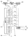
[実施例1]
図4は本発明の実施例1に係る蓄電システムの回路図である。本実施例では、定格電圧Vcのキャパシタバンクをm個直列接続して構成したキャパシタモジュール109において、h個のキャパシタバンクからなるキャパシタユニットごとにn個のタップを設け、バランス回路105を備えたキャパシタモジュールに充電器112を用いて電圧Vinにてフル充電(両端子間電圧=Vc×m)する場合について、m=100、n=51、h=2の場合を例として説明する。
[Example 1]
FIG. 4 is a circuit diagram of the power storage system according to
ここで、バランス回路は、蓄電モジュールを構成する蓄電バンクの充放電状態のばらつきを補正するための回路であり、充電及び放電の両方の期間に、各蓄電バンク間でのエネルギー伝送、つまりバランス動作を行うことができる。バランス回路は、大別してキャパシタを用いる方法、コイルを用いる方法、トランスを用いる方法に大別されるが、それぞれについての具体的な回路については種々のものが知られている(例えば特許文献2、非特許文献1参照)。 Here, the balance circuit is a circuit for correcting variations in the charge / discharge states of the storage banks constituting the storage module, and energy transfer between the storage banks, that is, a balance operation during both charging and discharging periods. It can be performed. The balance circuit is roughly classified into a method using a capacitor, a method using a coil, and a method using a transformer. Various specific circuits are known (for example, Patent Document 2, Non-patent document 1).
図4に戻り、スイッチS2a〜S51aはスイッチ群110を構成しており、キャパシタユニットの直列接続点の各々から取り出されたタップと充電器112の高電位側端子101との間に接続されている。C1〜C100はキャパシタバンクである。スイッチS2a〜S51aはいずれか一つのスイッチがオンしており、充電器112の高電位側端子101と直結されている。充電器の低電位側端子102はキャパシタモジュールのグラウンド0と固定接続されている。電圧検出回路106は、キャパシタモジュール109を構成する全てのキャパシタバンク又は一部のキャパシタバンクの電圧を検出する。この電圧検出結果を電圧判定回路107において基準電圧と比較し、その比較結果に基づいてスイッチ制御回路108がスイッチを切り替えることにより、充電器からの充電電圧はある任意の範囲内、例えば充電器の許容変動電圧内に収まるよう制御される。
Returning to FIG. 4, the switches S 2a to S 51a constitute a
図5は図4の構成において充電を行った場合の充電器電圧(上)及びキャパシタバンクの充電カーブ(下)である。ここではバランス回路の動作が理想的であり、いかなる条件においてもキャパシタモジュールを構成する各キャパシタバンクの電圧はバランス回路により均一に保たれているものとして説明を行う。 FIG. 5 shows a charger voltage (upper) and a capacitor bank charging curve (lower) when charging is performed in the configuration of FIG. Here, the operation of the balance circuit is ideal, and the description will be made on the assumption that the voltage of each capacitor bank constituting the capacitor module is kept uniform by the balance circuit under any conditions.
まず、スイッチ制御回路108によってスイッチS51aがオンにされると、スイッチS51aと接続されているタップの低電位側のキャパシタユニット、つまり全てのキャパシタバンクが充電器から直接充電される。
First, when the switch S 51a is turned on by the
充電が進行するにつれて、各キャパシタバンクの電圧は上昇してゆき、充電器電圧はVinに到達する。この時、各キャパシタバンクの電圧が均一であれば、各バンクの電圧はVin/100である。電圧検出回路106による電圧検出結果に基づいて電圧判定回路107により充電器電圧がVinに到達したと判断されると、スイッチ制御回路108はスイッチS51aをオフすると同時にS50aをオンし、これにより充電器112とキャパシタモジュール109を接続するタップを一つ分下位側へとシフトさせる。これにより、充電器電圧はキャパシタバンクC100とC99の電圧分つまり(2×Vin)/100だけ低くなる。この時、充電器からの電力はS50aと接続されているタップの低電位側のキャパシタユニットに供給され、つまりC1〜C98のキャパシタバンクが充電器から直接充電される。C100とC99のキャパシタバンクに関してはバランス回路経由でC1〜C98のキャパシタバンクから電荷を受け取ることにより充電される。
As the charge progresses, the voltage of each capacitor bank Yuki rises, the charger voltage reaches the V in. At this time, if the voltage of each capacitor bank is uniform, the voltage of each bank is V in / 100. When the charger voltage is the
充電が更に進行し、電圧検出回路106による電圧検出結果に基づいて電圧判定回路107により充電器電圧が再びVinに到達したと判断されると、スイッチ制御回路108はスイッチS50aをオフすると同時にS49aをオンすることで充電器112とキャパシタモジュール109を接続するタップを更に一つ分下位側へとシフトさせる。これにより、充電器電圧はキャパシタバンクC98とC97の電圧分つまり(2×Vin)/98だけ低くなる。この時、S49aと接続されているタップの低電位側のキャパシタユニット、つまりC1〜C96のキャパシタバンクが充電器から直接充電される。C97〜C100のキャパシタバンクに関してはバランス回路経由でC1〜C96のキャパシタバンクから電荷を受け取ることにより充電される。
Further progress charged, the charger voltage by the
以下同様に、スイッチS49a〜S2aを充電器電圧に応じて順次切り替えることにより、充電器電圧をある任意の範囲内に抑えつつ、各キャパシタを均一に充電することができる。 Similarly, by switching sequentially in accordance with the switch S 49a to S 2a to the charger voltage, while suppressing within any range of the charger voltage, it is possible to charge the respective capacitors uniformly.
以上の操作は充電器により直接充電されるキャパシタバンクの定格電圧の合計値が充電器による充電電圧Vinより小さくなるまで繰り返す。充電器により直接充電されるキャパシタバンクの直列数をxとすると、x×Vc<Vinを満たすまで上記のグループ化充電を繰り返す。以上の操作を繰り返すことで各キャパシタバンクへの充電がより均等に行われ、その結果、充電時間も短縮化することができる。 Above operations are repeated until the sum of the rated voltage of the capacitor bank is charged directly by the charger is smaller than the charging voltage V in by the charger. When the series number of capacitor banks directly charged by the charger is x, the above grouped charging is repeated until x × V c <V in is satisfied. By repeating the above operation, charging to each capacitor bank is performed more evenly, and as a result, the charging time can be shortened.
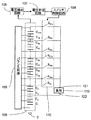
[実施例2]
図6は本発明の実施例2に係る蓄電システムの回路図である。同図において図4と対応する部分には同一符号を付し、実施例1と同様の部分の説明は省略する。
[Example 2]
FIG. 6 is a circuit diagram of a power storage system according to Embodiment 2 of the present invention. In the figure, parts corresponding to those in FIG.
実施例1は、充電器112の高電位側端子101がスイッチ群110を介してキャパシタモジュール109の各タップと接続された構成であるのに対し、本実施例は、充電器112の低電位側端子102とキャパシタモジュール109の間にS1b〜S50bから構成されるスイッチ群111を設けている。本実施例では、スイッチは、電圧検出回路106による電圧検出結果に基づいてスイッチ制御回路108によりS1b、S2b、・・・、S50bの順で切り替えられる。
In the first embodiment, the high-
以上の例では、バランス回路の動作が理想的であり、いかなる条件においてもキャパシタモジュールを構成する各キャパシタバンクの電圧はバランス回路により均一に保たれているという前提のもとで説明を行った。しかし、実際にはバランス回路の特性は理想的ではなく、均等化能力の制限やキャパシタバンクの等価直列抵抗の存在等により、キャパシタバンクの電圧のばらつきが発生することになる。 In the above example, the operation of the balance circuit is ideal, and the description has been made on the assumption that the voltage of each capacitor bank constituting the capacitor module is kept uniform by the balance circuit under any conditions. However, in practice, the characteristics of the balance circuit are not ideal, and variations in the voltage of the capacitor bank occur due to the limitation of the equalization capability and the presence of the equivalent series resistance of the capacitor bank.
実施例1の構成(m=25、n=26、h=1、C1とC25のキャパシタバンクの容量は他のキャパシタバンクの容量の2倍)にて均等化能力に制限があるバランス回路を用いてキャパシタバンクC5とC6との間の直列接続点に接続されるのスイッチS5aを介してキャパシタモジュールの充電を行った際における一部のキャパシタバンクC1、C5、C10、C15、C20、C25の充電波形の一例を図7に示す。充電過程において各キャパシタバンクは均一に充電されていないことが分かる。充電器から直接充電されないキャパシタバンク(S5aより高電位側のキャパシタバンクC6〜C25)は、直接充電されるキャパシタバンク(S5aより低電位側のキャパシタバンクC1〜C5)からバランス回路経由で電荷を受け取ることにより充電されるが、バランス回路が電荷を低電位側から高電位側へと電荷を受け渡す速度が十分でないため、高電位側のバンクの電圧は低電位側のバンクの電圧よりも低くなる傾向を示し、また、充電器から電気的に遠い位置のバンクほど充電の進行が遅くなる。バランス回路の機能により各バンクの電圧はいずれ収束するが、各バンクの電圧が十分に均等化されるまでには長い時間を要する。また、一部のキャパシタバンクC1で充電電圧のオーバーシュート現象(過充電)が見られる。 Balance circuit in which equalization ability is limited in the configuration of the first embodiment (m = 25, n = 26, h = 1, the capacitance of capacitor banks of C 1 and C 25 is twice that of other capacitor banks) Is used to charge the capacitor module via the switch S 5a connected to the series connection point between the capacitor banks C 5 and C 6, and some of the capacitor banks C 1 , C 5 , C 10 FIG. 7 shows an example of charging waveforms of C 15 , C 15 , C 20 and C 25 . It can be seen that the capacitor banks are not uniformly charged during the charging process. The capacitor banks not directly charged from the charger (capacitor banks C 6 to C 25 on the higher potential side than S 5a ) are balanced from the capacitor banks directly charged (capacitor banks C 1 to C 5 on the lower potential side than S 5a ). It is charged by receiving the charge via the circuit, but the balance circuit is not fast enough to transfer the charge from the low potential side to the high potential side. The bank is located farther from the charger, and the progress of charging becomes slower. Although the voltage of each bank eventually converges due to the function of the balance circuit, it takes a long time until the voltage of each bank is sufficiently equalized. In addition, a charge voltage overshoot phenomenon (overcharge) is observed in some capacitor banks C1.
[実施例3]
図8は本発明の実施例3に係る蓄電システムの回路図である。同図において図4と対応する部分には同一符号を付し、実施例1と同様の部分の説明は省略する。
[Example 3]
FIG. 8 is a circuit diagram of a power storage system according to Example 3 of the present invention. In the figure, parts corresponding to those in FIG.
実施例1は充電器の低電位側端子102とキャパシタモジュール109のグラウンド0が直接接続された構成であるのに対し、本実施例では、低電位側端子102は、キャパシタモジュール109のグラウンド0と直接接続されておらず、キャパシタバンクC2とC3の直列接続点と固定接続されている。
In the first embodiment, the low
本実施例では、スイッチは、電圧検出回路106による電圧検出結果に基づいてスイッチ制御回路108によりS51a、S50a、・・・、S3aの順で切り替えられる。
In this embodiment, the switches are switched in the order of S 51a , S 50a ,..., S 3a by the
実施例1の構成における充電過程の末期では、スイッチS2aがオンしており、C1とC2の2つのキャパシタバンクが直接充電され、その他のキャパシタバンクはバランス回路経由で充電が行われている。この時、C100のキャパシタバンクは充電器112から最も電気的に離れており(98バンク分)、バランス回路の特性が理想的ではない場合、充電過程において最も低い電圧を示すことになる。 At the end of the charging process in the configuration of the first embodiment, the switch S 2a is on, the two capacitor banks C 1 and C 2 are directly charged, and the other capacitor banks are charged via the balance circuit. Yes. At this time, the capacitor bank of the C 100 is the most electrically separated from the charger 112 (98 banks min), when the characteristic of the balancing circuit is not ideal, would indicate a lowest voltage in the charging process.
実施例1では充電器112の低電位側端子102がキャパシタモジュール109のグラウンド0と接続された構成であったが、本実施例のように充電器の低電位側端子とキャパシタモジュールのグラウンド端子が直接接続されていない構成においては、充電末期におけるバランス回路とキャパシタバンクの電気的距離を実施例1の構成と比べて短くすることが可能である。
In the first embodiment, the low
本実施例では充電器の低電位側端子102はキャパシタバンクC2とC3の直列接続点と固定接続されているため、充電器112はC1とC2のキャパシタバンクを直接充電することは出来ない。しかし、C1とC2のキャパシタバンクはバランス回路105を経由して他のキャパシタバンクから電荷を受け取ることにより充電される。
In this embodiment, since the low
本実施例における充電過程の末期では、スイッチS3aがオンとなり、C3とC4のキャパシタバンクが直接充電され、その他のバンクはバランス回路経由で充電が行われる。充電器112から最も電気的に離れているC100のキャパシタバンクは、実施例1の図4の構成においては98バンク分離れていたのに対して、本実施例の構成では充電器112の低電位側端子102が2バンク分だけ高電位側(C2とC3の直接接続点)に接続されているため、実施例1の図4の構成よりも充電器に2バンク分だけ近い96バンク分の距離である。よって、充電過程の末期において実施例1の図4の構成よりもキャパシタバンクの電圧ばらつきを小さく抑えることが可能となる。
At the end of the charging process in this embodiment, the switch S 3a is turned on, the capacitor banks of C 3 and C 4 are directly charged, and the other banks are charged via the balance circuit. The capacitor bank of C 100 that is the most electrically separated from the
本実施例の構成で充電過程の末期においてキャパシタバンクの電圧ばらつきが最も小さくなるようにするには、充電器112の高電位側端子101と低電位側端子102をそれぞれS27aとS26a、もしくはS26aとS25aに接続すればよい。
In the configuration of this embodiment, in order to minimize the voltage variation of the capacitor bank at the end of the charging process, the high-
以上の実施例において、スイッチの位置や個数等のレイアウトは、必要に応じて適宜変更することができる。 In the above embodiment, the layout of the positions and the number of switches can be changed as necessary.
[実施例4]
図9は本発明の実施例4に係る蓄電システムの回路図である。同図において図4と対応する部分には同一符号を付し、実施例1と同様の部分の説明は省略する。
[Example 4]
FIG. 9 is a circuit diagram of a power storage system according to Embodiment 4 of the present invention. In the figure, parts corresponding to those in FIG.
上述のように、実施例3の構成で充電過程の末期においてキャパシタバンクの電圧ばらつきが最も小さくなるようにするには、充電器112の高電位側端子101と低電位側端子102をそれぞれスイッチS27aとS26a、もしくはスイッチS26aとS25aに接続すればよいことになる。しかし、この場合は充電の初期においても充電器から電気的に離れたバンク(C1などの低電位側に位置するバンク)が存在することになるためバンク、充電末期のばらつきは低減される半面、充電の初期段階においても電圧ばらつきが発生してしまう。本実施例は、これに限られるものではないが、このような問題点を解決するものである。
As described above, in the configuration of the third embodiment, in order to minimize the voltage variation of the capacitor bank at the end of the charging process, the high
本実施例では、実施例1の場合と同様に、定格電圧Vcのキャパシタバンクをm個直列接続しh個のキャパシタバンクからなるキャパシタユニットごとにn個のタップ(それぞれn個のスイッチで構成される第一スイッチ群と第二スイッチ群)を設け、バランス回路105を備えた蓄電装置に充電器112を用いて電圧Vinにてフル充電(両端子間電圧=Vc×m)する場合について、m=100、n=51、h=2を例として説明する。
In this embodiment, as in the case of the first embodiment, m capacitor banks of rated voltage Vc are connected in series, and n taps (each composed of n switches) are provided for each capacitor unit composed of h capacitor banks. that first switch group and the second switch group) is provided, for the case of full charge (voltage between both terminals = Vc × m) by the voltage V in by using the
スイッチS2a〜S51aは第一スイッチ群110’を、スイッチS1b〜S50bは第二スイッチ群111’をそれぞれ構成しており、キャパシタユニットの直列接続点の各々から取り出されたタップと充電器112の高電位側端子101、低電位側端子102との間にそれぞれ接続されている。
The switches S 2a to S 51a constitute a
次に、本実施例の動作を説明する。まず充電の初期段階では、スイッチ制御回路108によってスイッチS51aとS1bがオンにされ充電が行われる。この時、キャパシタモジュール109の全てのキャパシタバンクが充電器112から直接充電される。
Next, the operation of this embodiment will be described. First, in the initial stage of charging, the switches S 51a and S 1b are turned on by the
充電が進行するにつれて、各キャパシタバンクの電圧は上昇してゆき、充電器電圧はVinに到達する。電圧検出回路106による電圧検出結果に基づいて電圧判定回路107により充電器電圧がVinに到達したと判断されると、スイッチ制御回路108はスイッチS51aをオフすると同時にスイッチS50aをオンし、これにより充電器112の高電位側端子101とキャパシタモジュール109を接続するタップを一つ分下位側へとシフトさせる。この時、C1〜C98のキャパシタバンクは充電器によりバランス回路を介さずに直接充電され、C99とC100のキャパシタバンクはバランス回路経由で充電が行われる。
As the charge progresses, the voltage of each capacitor bank Yuki rises, the charger voltage reaches the V in. When the charger voltage is the
さらに充電が進行し、電圧検出回路106による電圧検出結果に基づいて電圧判定回路107により充電器電圧が再びVinに到達したと判断されると、スイッチ制御回路108はスイッチS1bをオフすると同時にスイッチS2bをオンし、これにより充電器112の低電位側端子102とキャパシタモジュール109を接続するタップを一つ分上位側へとシフトさせる。この時、C3〜C98のキャパシタバンクは充電器によりバランス回路を介さずに直接充電され、C1、C2、C99、C100のキャパシタバンクはバランス回路経由で充電が行われる。
Charging progresses further, when the charger voltage by the
このように、充電の進行に伴い、充電器の高電位側端子101と低電位側端子102に接続されるタップを順次切り替えるがこのとき、図10に示すようにキャパシタモジュール109を構成する直列接続キャパシタバンクの中央付近のバンク(C50、C51)が充電器により直接充電されるキャパシタバンクの中央となるようにする。図10は、C50とC51が充電器により直接充電されるキャパシタバンクの中央となるようにスイッチを順次切り替えてゆき、S39aとS13bが選択され、C25〜C76の計52のキャパシタバンクが充電器により直接充電されている状態を示している(簡略化のため、バランス回路や非動作のスイッチ等は省略している)。その他のC1〜C24とC77〜C100のキャパシタバンクはバランス回路経由で充電が行われる。このようなスイッチの切り替えを行うことにより、バランス回路経由で充電されるキャパシタバンクと充電器の電気的距離を極力短くなるようにすることができる。
As described above, the taps connected to the high-
さらに充電が進み、充電器により直接充電されるキャパシタバンクの直列数がキャパシタモジュール109におけるキャパシタバンクの総直列数mの半分よりも少なくなった場合、キャパシタモジュール109のキャパシタバンクを、m×1/4、m×3/4、つまりC25、C75あたりのバンクが充電器により直接充電される直列接続キャパシタバンクの中心になるように2つのグループにグループ化し、グループ化された2つのグループのそれぞれに対して、スイッチ制御回路108はスイッチを選択し、時分割で充電器により充電を行う。
When the charging further proceeds and the series number of capacitor banks directly charged by the charger is less than half of the total series number m of capacitor banks in the
図11はC25、C75あたりのバンクが充電器により直接充電される直列接続キャパシタバンクの中心になるように、スイッチ制御回路108がスイッチS47aとS29b、スイッチS22aとS4bを選択し、C57〜C92のキャパシタバンクとC7〜C42のキャパシタバンクが交互に時分割で充電器により直接充電されている状態を示している。
In FIG. 11, the
スイッチ制御回路108がスイッチS47aとS29bを介して充電を行っている期間はC57〜C92のキャパシタバンクは充電器により直接充電され、その他のキャパシタバンクはバランス回路経由で充電される。また、スイッチ制御回路108がS22aとS4bを介して充電を行っている期間はC7〜C42のキャパシタバンクが充電器により直接充電され、その他のキャパシタバンクはバランス回路経由で充電されることになる。このとき、各キャパシタバンクの電圧をなるべく均一に保つという観点において、各キャパシタユニットが充電器により直接充電される時間が等しくなるようS47aとS29b、S22aとS4bを交互に切り替えるのが望ましい。
During the period when the
以下同様にして、さらに充電が進み、充電器により直接充電されるキャパシタバンクの直列数がキャパシタモジュール109におけるキャパシタバンクの総直列数の1/3よりも少なくなった場合、キャパシタモジュール109のキャパシタバンクを、m×1/6、m×3/6、m×5/6、つまりC17、C50、C83あたりのバンクが充電器により直接充電される直列接続キャパシタバンクの中心になるように3つのグループにグループ化し、グループ化された3つのグループのそれぞれに対して、スイッチ制御回路108はスイッチを選択し、時分割で充電器により充電を行う。図12は、スイッチ制御回路108がスイッチS51aとS35b、スイッチS34aとS18b、スイッチS17aとS1bを選択し、C69〜C100とC35〜C66とC1〜C32のキャパシタバンクが交互に充電器により直接充電されている状態を示している。
Similarly, when the charging further proceeds and the series number of capacitor banks directly charged by the charger is less than 1/3 of the total series of capacitor banks in the
同様に、さらに充電が進み、充電器により直接充電されるキャパシタバンクの直列数がキャパシタモジュール109におけるキャパシタバンクの総直列数の1/4よりも少なくなった場合、キャパシタモジュール109のキャパシタバンクを、m×1/8、m×3/8、m×5/8、m×7/8、つまりC13、C38、C63、C88あたりのバンクが充電器により直接充電される直列接続キャパシタバンクの中心になるように4つのグループにグループ化し、グループ化された4つのグループのそれぞれに対して、スイッチ制御回路108はスイッチを選択し、時分割で充電器により充電を行う。図13は、スイッチ制御回路108がスイッチS48aとS42b、スイッチS35aとS29b、スイッチS23aとS17b、スイッチS10aとS4bを選択し、C83〜C94、C57〜C68、C33〜C44、C7〜C18のキャパシタバンクが交互に充電器により直接充電されている状態を示している。
Similarly, when charging further proceeds and the series number of capacitor banks directly charged by the charger is less than 1/4 of the total series number of capacitor banks in the
いずれのグループ化充電段階においても、各キャパシタバンクの電圧をなるべく均一に保つという観点において、各キャパシタユニットが充電器により直接充電される時間が等しくなるようにスイッチを切り替えるのが望ましい。 In any grouped charging stage, from the viewpoint of keeping the voltage of each capacitor bank as uniform as possible, it is desirable to switch the switches so that the time for which each capacitor unit is directly charged by the charger is equal.
以上の操作は充電器により直接充電されるバンクの定格電圧の合計値が充電器による充電電圧Vinより小さくなるまで繰り返す。充電器により直接充電されるキャパシタバンクの直列数をxとすると、x×Vc<Vinを満たすまで上記のグループ化充電を繰り返す。以上の操作を繰り返すことで各キャパシタバンクへの充電がより均等に行われ、その結果、充電時間も短縮化することができる。 Above operations are repeated until the sum of the rated voltage of the bank is charged directly by the charger is smaller than the charging voltage V in by the charger. When the series number of capacitor banks directly charged by the charger is x, the above grouped charging is repeated until x × V c <V in is satisfied. By repeating the above operation, charging to each capacitor bank is performed more evenly, and as a result, the charging time can be shortened.
上の実施例と同様の構成で、m=25、n=26、h=1、C1とC25のキャパシタバンクの容量は他のキャパシタバンクの容量の2倍の条件にて、均等化能力に制限があるバランス回路を用いた場合における一部のキャパシタバンクC1、C5、C10、C15、C20、C25の充電波形の一例を図14Aに示す。各キャパシタバンクの充電波形がよく一致しており、各キャパシタバンクが均一に充電されていることが分かる。また、各キャパシタバンクの充電時間も短いことが分かる。実施例1の例の図7と比較すると、格段の改善がなされていることが分かる。 With the same configuration as the above embodiment, m = 25, n = 26, h = 1, and the capacity of the capacitor banks of C 1 and C 25 is equal to the capacity of other capacitor banks. FIG. 14A shows an example of charging waveforms of some capacitor banks C 1 , C 5 , C 10 , C 15 , C 20 , and C 25 in the case where a balance circuit having a limitation is used. It can be seen that the charge waveforms of the capacitor banks are in good agreement, and the capacitor banks are charged uniformly. It can also be seen that the charging time of each capacitor bank is short. Compared with FIG. 7 of the example of Example 1, it can be seen that the improvement is made significantly.
上の実施例では、蓄電モジュールを構成する複数の蓄電バンクがグループ化されていない状態から充電を開始したが、蓄電モジュールを構成する複数の蓄電バンクを複数のグループ化した状態から充電を開始することもできる。この場合、上の実施例では、充電器により直接充電されるキャパシタユニットの数が減るようにスイッチの切替えが行われたが、複数のグループの各々について同じキャパシタユニットに対して充電器による直接充電を時分割で繰り返し行う構成としても、バランス回路を介して充電されるキャパシタユニットに対する電気的距離を短くすることができるため、各キャパシタバンクへの充電をより均等に行うことができる。 In the above embodiment, charging is started from a state where a plurality of power storage banks constituting the power storage module is not grouped, but charging is started from a state where a plurality of power storage banks constituting the power storage module are grouped. You can also. In this case, in the above embodiment, the switch is switched so that the number of capacitor units directly charged by the charger is reduced. However, the same capacitor unit is directly charged by the charger for each of the plurality of groups. Even in a configuration in which these are repeatedly performed in a time-sharing manner, the electrical distance to the capacitor unit charged through the balance circuit can be shortened, so that charging to each capacitor bank can be performed more evenly.
図12と同様の構成で、m=25、n=26、h=1、C1とC25のキャパシタバンクの容量は他のキャパシタバンクの容量の2倍、C3−C7、C11−C15、C19−C23の3グループの条件にて、均等化能力に制限があるバランス回路を用いて、この3グループの各々について同じC3−C7、C11−C15、C19−C23に対して、充電器よる直接充電を時分割で繰り返し行った際における一部のキャパシタバンクC1、C5、C10、C15、C20、C25の充電波形の一例を図14Bに示す。各キャパシタバンクの充電波形が非常によく一致しており、各キャパシタバンクが均一に充電されていることが分かる。実施例1の例の図7と比較すると、格段の改善がなされていることが分かる。また、上の実施例の図14Aと比較すると、充電に時間を要するものの、各キャパシタバンクをより均一に使用することができることが分かる。
The same configuration as FIG. 12, m = 25, n = 26, h = 1, the capacitance of the capacitor bank C 1 and C 25 2 times the volume of the other capacitor bank, C 3 -C 7, C 11 - Under the conditions of three groups of C 15 and C 19 to C 23, the same C 3 -C 7 , C 11 -C 15 , and C 19 are used for each of these three groups by using a balance circuit with limited equalization ability. An example of charging waveforms of some capacitor banks C 1 , C 5 , C 10 ,
本実施例において、スイッチの位置や個数等のレイアウトは、複数のタップのうちの一つが充電器の一方の端子又は他方の端子と接続されるように、且つ充電器からバランス回路を介さずに直接充電される複数の蓄電ユニットの数を制御するように順次スイッチを切り替えることができるような構成であれば、適宜変更することができる。変更例としては、図15のようなものが考えられる。また、更に、例えば、太陽電池のような出力電圧が変動する場合のある充電器の場合には、出力電圧の増加に伴い、充電過程において、充電器から直接充電される蓄電ユニットの数を増やすようにスイッチを切り替える場合も考えられる。したがって、電圧検出回路による電圧検出結果に基づいて、充電器から直接充電される蓄電ユニットの数を減少させ、一定にし、又は増加させるようなスイッチの切替えを適宜組み合わせることも考えられる。 In this embodiment, the layout of the position and number of switches is such that one of the plurality of taps is connected to one terminal or the other terminal of the charger, and without a balance circuit from the charger. The configuration can be changed as appropriate as long as the switch can be sequentially switched so as to control the number of the plurality of power storage units that are directly charged. As a modification example, the one shown in FIG. 15 can be considered. Furthermore, for example, in the case of a charger such as a solar battery in which the output voltage may fluctuate, as the output voltage increases, the number of power storage units that are directly charged from the charger is increased in the charging process. It is also conceivable to switch the switch as described above. Therefore, based on the voltage detection result by the voltage detection circuit, it is conceivable to appropriately combine switching of switches such that the number of power storage units directly charged from the charger is reduced, made constant, or increased.
本実施例において、充電を開始する蓄電ユニットの位置、蓄電モジュールを構成する複数の蓄電バンクの各グループ化段階におけるグループの数や各グループにおける蓄電バンクの個数等の構成は任意に選択することができる。 In this embodiment, the configuration of the storage unit where charging starts, the number of groups in each grouping stage of the plurality of storage banks constituting the storage module, the number of storage banks in each group, and the like can be arbitrarily selected. it can.
以上の実施例においては、スイッチ制御回路108によるスイッチ切替えのタイミングが、電圧検出回路106による電圧検出結果に基づいて充電器電圧がVinに到達したと判断されたときであったが、充電器電圧が到達したと判断される電圧はVin未満の任意の電圧とすることができる。
Or more in the embodiments, the timing of the switch by the
ここまでは充電動作について述べたが、本発明の技術は負荷に対して放電を行う場合に対しても適用することができる。 The charging operation has been described so far, but the technique of the present invention can also be applied to the case where the load is discharged.
[実施例5]
図16は、本発明の実施例5に係る蓄電システムの回路図である。同図において図4と対応する部分には同一符号を付し、実施例1と同様の部分の説明は省略する。
[Example 5]
FIG. 16 is a circuit diagram of a power storage system according to Example 5 of the present invention. In the figure, parts corresponding to those in FIG. 4 are denoted by the same reference numerals, and description of parts similar to those in the first embodiment is omitted.
本実施例の構成は上記実施例1の構成における充電器を負荷113に置き換えたものであり、基本的には充電時とは逆の動作(スイッチの切り替え順序等)を実施することで、出力電圧変動を抑えつつ、各キャパシタバンクを均一に放電させることが可能である。
The configuration of the present embodiment is obtained by replacing the charger in the configuration of the first embodiment with the
図17は図16の構成にて放電を行った際における動作波形である。実施例1の図4〜図5で説明した充電動作とは逆に、S2aがオンになっている状態からスタートし、電圧検出回路106で検出した負荷電圧を電圧判定回路107により判定することによってスイッチ制御回路108が負荷電圧がある任意の値(例えば、負荷の許容下限電圧Vlow)を下回らないようスイッチを上位側へと順次切り替えることにより負荷電圧をある任意の範囲内に抑える。負荷と直接接続されるキャパシタバンク(S2aがオンの場合、C1とC2)は負荷に対して直接放電し、その他のキャパシタバンクはバランス回路を通じて放電する。
FIG. 17 shows operation waveforms when discharging is performed with the configuration of FIG. Contrary to the charging operation described with reference to FIGS. 4 to 5 of the first embodiment, the
[実施例6]
図18は、本発明の実施例6に係る蓄電システムの回路図である。同図において図16と対応する部分には同一符号を付し、実施例5と同様の部分の説明は省略する。
[Example 6]
FIG. 18 is a circuit diagram of a power storage system according to Embodiment 6 of the present invention. In the figure, parts corresponding to those in FIG.
上記実施例5は負荷113の高電位側端子121とキャパシタモジュール109の間にスイッチ群110を設けた構成であるのに対し、本実施例は、低電位側端子122とキャパシタモジュール109の間にスイッチ群111を設けている。本実施例では、スイッチは、電圧検出回路106による電圧検出結果に基づいてスイッチ制御回路108によりS50b、S49b、・・・、S1bの順で切り替えられる。
In the fifth embodiment, the
[実施例7]
図19は、本発明の実施例7に係る蓄電システムの回路図である。同図において図16と対応する部分には同一符号を付し、実施例5と同様の部分の説明は省略する。
[Example 7]
FIG. 19 is a circuit diagram of a power storage system according to Example 7 of the present invention. In the figure, parts corresponding to those in FIG.
上記実施例5は負荷113の低電位側端子122とキャパシタモジュール109のグラウンド0が直接接続された構成であるのに対し、本実施例では、低電位側端子122は、キャパシタモジュール109のグラウンド0と直接接続されておらず、キャパシタバンクC2とC3の直列接続点と固定接続されている。
In the fifth embodiment, the low
本実施例では、スイッチは、電圧検出回路106による電圧検出結果に基づいてスイッチ制御回路108によりS3a、S4a、・・・、S51aの順で切り替えられる。
In this embodiment, the switch is switched in the order of S 3a , S 4a ,..., S 51a by the
実施例5では負荷113の低電位側端子122がキャパシタモジュール109のグラウンド0と接続された構成であったが、本実施例のように負荷の低電位側端子とキャパシタモジュールのグラウンド端子が直接接続されていない構成においては、放電初期における負荷とキャパシタバンクの電気的距離を実施例5の構成と比べて短くすることが可能である。すなわち、本実施例における放電過程の初期では、スイッチS3aがオンとなり、C3とC4のキャパシタバンクから負荷へ直接放電され、C1、C2、C5〜C100のキャパシタバンクはバランス回路経由で放電が行われる。負荷113から最も電気的に離れているC100のキャパシタバンクは、実施例5においては98バンク分離れていたのに対して、本実施例の構成では負荷113の低電位側端子122が2バンク分だけ高電位側(C2とC3の直接接続点)に接続されているため、実施例5の構成よりも充電器に2バンク分だけ近い96バンク分の距離である。よって、放電過程の初期において実施例5の場合よりもキャパシタバンクの電圧ばらつきを小さく抑えることが可能となる。
In the fifth embodiment, the low
本実施例の構成で放電過程の初期においてキャパシタバンクの電圧ばらつきが最も小さくなるようにするには、負荷113の高電位側端子121と低電位側端子122をそれぞれスイッチS27aとS26a、もしくはスイッチS26aとS25aに接続すればよい。
In the configuration of this embodiment, in order to minimize the voltage variation of the capacitor bank at the initial stage of the discharging process, the high
以上の実施例5〜7において、スイッチの位置や個数等のレイアウトは、必要に応じて適宜変更することができる。 In the above Examples 5 to 7, the layout of the positions and number of switches can be changed as needed.
[実施例8]
図20は、本発明の実施例8に係る蓄電システムの回路図である。同図において図16と対応する部分には同一符号を付し、実施例5と同様の部分の説明は省略する。
[Example 8]
FIG. 20 is a circuit diagram of a power storage system according to Example 8 of the present invention. In the figure, parts corresponding to those in FIG. 16 are denoted by the same reference numerals, and description of parts similar to those in the fifth embodiment is omitted.
本実施例の構成は実施例4の構成における充電器を負荷113に置き換えたものであり、基本的には充電時とは逆の動作(スイッチの切り替え順序や、キャパシタバンクのグループ化順序等)を実施することで、出力電圧変動を抑えつつ、各キャパシタバンクを均一に放電させることが可能である。本実施例では、実施例4の場合と同様に、定格電圧Vcのキャパシタバンクをm個直列接続しh個のバンクからなるキャパシタユニットごとにn個のタップ(それぞれn個のスイッチで構成される第一スイッチ群と第二スイッチ群)を設け、バランス回路105を備えた蓄電装置において、負荷113に対して放電する場合について、m=100、n=51、h=2の場合を例として説明する。
The configuration of the present embodiment is obtained by replacing the charger in the configuration of the fourth embodiment with a
スイッチS2a〜S51aは第一スイッチ群110’を、スイッチS1b〜S50bは第二スイッチ群111’をそれぞれ構成しており、キャパシタユニットの直列接続点の各々から取り出されたタップと負荷113の高電位側端子121、低電位側端子122との間にそれぞれ接続されている。
The switches S 2a to S 51a constitute a
次に、本実施例の動作を説明する。上述のように本実施例は基本的には充電時の実施例である実施例4の動作とは逆の動作を行うものである。そこで、ここでは例として、放電スタート時のグループ数が4つの状態、すなわちキャパシタモジュールを構成するキャパシタバンクが4つのグループにグループ化された状態からスタートする構成で説明する。 Next, the operation of this embodiment will be described. As described above, the present embodiment basically performs an operation opposite to that of the fourth embodiment, which is an embodiment during charging. Therefore, here, as an example, a description will be given of a state in which the number of groups at the start of discharge is four, that is, a configuration in which the capacitor banks constituting the capacitor module are grouped into four groups.
まず放電の初期段階では、キャパシタモジュール109のキャパシタバンクを、m×1/8、m×3/8、m×5/8、m×7/8、つまりC13、C38、C63、C88あたりのバンクが負荷へ直接放電する直列接続キャパシタバンクの中心になるように4つのグループにグループ化し、グループ化された4つのグループのそれぞれに対して、スイッチ制御回路108は、各グループを構成する直列接続キャパシタバンクの中央付近のバンク(C13、C38、C63、C88あたりのバンク)が負荷へ直接放電する直列接続キャパシタバンク群の中心になるようにスイッチを選択し、時分割で負荷へ放電を行う。
First, at the initial stage of discharge, the capacitor bank of the
図21は、スイッチ制御回路108がスイッチS8aとS7b、S20aとS19b、S33aとS32b、S45aとS44bを選択し、C13〜C14、C37〜C38、C63〜C64、C87〜C88のキャパシタバンクが交互に負荷に対して放電している状態を示している。この4つの各グループの動作について、キャパシタバンクC13を含むグループを例にとり説明する。まずS8aとS7bがオンになっている状態からスタートする。放電が進行するにつれて、各キャパシタバンクの電圧は下降してゆき、電圧検出回路106による電圧検出結果に基づいて電圧判定回路107により負荷電圧が負荷の許容下限電圧Vlowに到達したと判断されると、スイッチ制御回路108はスイッチS8aをオフすると同時にスイッチS9aをオンし、これにより負荷113の高電位側端子121とキャパシタモジュール109を接続するタップを一つ分上位側へとシフトさせる。この時、C13〜C16のキャパシタバンクはバランス回路を介さずに負荷へ直接放電し、その他のキャパシタバンクはバランス回路経由で放電を行う。さらに放電が進行し、電圧検出回路106による電圧検出結果に基づいて電圧判定回路107により負荷電圧が再びVlowに到達したと判断されると、スイッチ制御回路108はスイッチS7bをオフすると同時にスイッチS6bをオンし、これにより負荷113の低電位側端子122とキャパシタモジュール109を接続するタップを一つ分下位側へとシフトさせる。この時、C11〜C16のキャパシタバンクはバランス回路を介さずに負荷へ直接放電し、その他のキャパシタバンクはバランス回路経由で放電を行う。このようなスイッチの切り替えを行うことにより、各キャパシタバンクが負荷へ直接放電する時間をなるべく等しくすることができ、各キャパシタバンクの電圧をなるべく均一に保つという観点において望ましい。
In FIG. 21, the
放電が進み、負荷へ直接放電するキャパシタバンクの直列数が増加しキャパシタモジュール109におけるキャパシタバンクの総直列数に対して所定の割合(例えば1/4)になった場合、キャパシタモジュール109のキャパシタバンクを、m×1/6、m×3/6、m×5/6、つまりC17、C50、C83あたりのキャパシタバンクが負荷へ直接放電する直列接続キャパシタバンクの中心になるように3つのグループにグループ化し、グループ化された3つのグループのそれぞれに対して、スイッチ制御回路108は、各グループを構成する直列接続キャパシタバンクの中央付近のバンク(C17、C50、C83あたりのバンク)が負荷へ直接放電する直列接続キャパシタバンクの中心になるようにスイッチを選択し、時分割で負荷へ放電を行う。この時、前記図21の4つのグループ化した放電により、キャパシタバンクの電圧がある程度低下しているため、負荷に直接接続されるキャパシタバンクの電圧の合計値が負荷の許容下限電圧よりも高くなるようスイッチを選択する必要がある。図22は、例として、スイッチ制御回路108がスイッチS15aとS3b、スイッチS32aとS20b、スイッチS49aとS37bを選択し、C5〜C28、C39〜C62、C73〜C96のキャパシタバンクが交互に負荷へ直接放電を行っている状態を示している。各グループ内でのスイッチ制御回路108によるスイッチの切替えは、上記と同様であるので説明を省略する。
When discharge progresses and the series number of capacitor banks that directly discharge to the load increases and reaches a predetermined ratio (for example, 1/4) with respect to the total series number of capacitor banks in the
以下同様の操作を繰り返してゆき、各グループにおける負荷へ直接放電するキャパシタバンクの電圧の合計値が負荷の許容下限電圧Vlowを下回るまで繰り返す。この操作が繰り返された場合、最終的にはS51aとS1bがオンの状態となり全てのキャパシタバンクが負荷へと直接放電を行う、つまりグループが1つになる。図23は、スイッチS39aとS13bを選択し、C25〜C76のキャパシタバンクが負荷に直接放電し、他のバンクはバランス回路を介して放電している状態を示している。放電時におけるキャパシタバンクの電圧をVdisとすると、m×Vdis<Vlowを満たすまで上記のグループ化放電を繰り返す。以上の操作を繰り返すことで各キャパシタバンクへからの放電がより均等に行われ、その結果、放電時間も長期化することができる。 Thereafter, the same operation is repeated until the total value of the voltage of the capacitor bank that directly discharges to the load in each group falls below the allowable lower limit voltage V low of the load. When this operation is repeated, S51a and S1b are finally turned on and all capacitor banks are directly discharged to the load, that is, one group is formed. Figure 23 selects the switch S 39a and S 13b, and discharged directly to the load capacitor banks C 25 -C 76, other banks shows a state in which discharges through a balance circuit. Assuming that the voltage of the capacitor bank at the time of discharge is V dis , the above grouped discharge is repeated until m × V dis <V low is satisfied. By repeating the above operation, the discharge from each capacitor bank is performed more evenly, and as a result, the discharge time can be prolonged.
いずれのグループ化放電段階においても、各キャパシタバンクの電圧をなるべく均一に保つという観点において、各キャパシタバンクが負荷へ直接放電する時間が等しくなるようにスイッチを切り替えるのが望ましい。 In any grouped discharge stage, it is desirable to switch the switches so that the time for each capacitor bank to discharge directly to the load is equal from the viewpoint of keeping the voltage of each capacitor bank as uniform as possible.
上の実施例では、負荷へ直接放電されるキャパシタユニットの数が増えるようにスイッチの切替えが行われたが、複数のグループの各々について同じキャパシタユニットが負荷への直接放電を時分割で繰り返し行う構成としても、バランス回路を介して放電されるキャパシタユニットに対する電気的距離を短くできるため、各キャパシタバンクからの放電をより均等に行うことができる。 In the above embodiment, switching is performed so that the number of capacitor units directly discharged to the load is increased. However, the same capacitor unit repeatedly performs direct discharge to the load in a time division manner for each of a plurality of groups. Even in the configuration, since the electrical distance to the capacitor unit discharged via the balance circuit can be shortened, the discharge from each capacitor bank can be performed more evenly.
本実施例においても実施例4と同様に、スイッチの位置や個数等のレイアウトは、複数のタップのうちの一つが負荷の一方の端子又は他方の端子と接続されるように、且つバランス回路を介さずに負荷へ直接放電する複数の蓄電ユニットの数を制御するように順次スイッチを切り替えることができるような構成であれば、任意に変更することができる。また、例えば、負荷への放電と充電器からの充電を同時に行う場合において、充電器からの充電パワーが負荷への放電パワーを上回るときに、放電過程において、負荷へ直接放電する蓄電ユニットの数を減らすようにスイッチを切り替える場合も考えられる。したがって、電圧検出回路による電圧検出結果に基づいて、負荷へ直接放電される蓄電ユニットの数を減少させ、一定にし、又は増加させるようなスイッチの切替えを適宜組み合わせることも考えられる。 Also in the present embodiment, as in the fourth embodiment, the layout of the position and number of switches is such that one of the plurality of taps is connected to one terminal of the load or the other terminal, and the balance circuit is provided. Any configuration can be used as long as the switches can be sequentially switched so as to control the number of the plurality of power storage units that are directly discharged to the load without intervention. In addition, for example, when discharging to the load and charging from the charger are performed at the same time, when the charging power from the charger exceeds the discharging power to the load, the number of power storage units that directly discharge to the load in the discharging process It is also conceivable to switch the switches so as to reduce the number of switches. Therefore, based on the voltage detection result by the voltage detection circuit, it is conceivable to appropriately combine switching of switches such that the number of power storage units directly discharged to the load is reduced, made constant, or increased.
本実施例において、放電を開始する蓄電ユニットの位置、蓄電モジュールを構成する複数の蓄電バンクの各グループ化段階におけるグループの数や各グループにおける蓄電バンクの個数等の構成は任意に選択することができる。 In this embodiment, the configuration of the storage unit starting discharge, the number of groups in each grouping stage of the plurality of storage banks constituting the storage module, the number of storage banks in each group, and the like can be arbitrarily selected. it can.
また、上記実施例においては、スイッチ制御回路108によるスイッチ切替えのタイミングが、電圧検出回路106による電圧検出結果に基づいて負荷がVlowに到達したと判断されたときであったが、負荷電圧が到達したと判断される電圧はVlowよりも大きく負荷の許容上限電圧以下の任意の電圧とすることができる。
In the above embodiment, the switch switching timing by the
以上の実施例では電圧検出回路106によりキャパシタモジュール109を構成する各キャパシタバンクの電圧を検出し、その検出結果を元に電圧判定回路107において基準電圧と比較し、その比較結果を元にスイッチ制御回路108によりスイッチを切り替えることにより、充電器からの充電電圧又は負荷への放電電圧をある任意の範囲内に収まるよう制御する場合について述べてきた。しかし、キャパシタモジュール109を構成する各キャパシタバンクの電圧を検出する代わりに、充電器からの充電電圧又は負荷への放電電圧を検出し、その検出結果を元にスイッチの切り替え制御を行ってもよい。この場合においてもキャパシタバンク電圧や充電器からの充電電圧ならびに負荷への放電電圧はこれまでに説明してきた特性と同様の傾向を示す。
In the above embodiment, the
以上の実施例においては、h個のキャパシタバンクからなるキャパシタユニットごとにn個のタップを設けた構成について述べたが、キャパシタユニットを構成するキャパシタバンクの数(タップを設ける間隔)は、ある位置ではh個、ある位置はh+1個といったように、位置によって任意に変更してもよい。 In the above embodiment, the configuration in which n taps are provided for each capacitor unit composed of h capacitor banks has been described. However, the number of capacitor banks constituting the capacitor unit (the interval at which taps are provided) is set at a certain position. Then, it may be arbitrarily changed depending on the position, such as h, and a certain position is h + 1.
以上の実施例においては、各キャパシタバンクの定格電圧はVcであったが、あるキャパシタバンクはVc'、あるキャパシタバンクはVc''といったように、各キャパシタバンクによって定格電圧を任意に変更してもよい。 In the above embodiments, the rated voltage of each capacitor bank is V c , but the rated voltage is arbitrarily changed depending on each capacitor bank, such as Vc ′ for a certain capacitor bank and V c ″ for a certain capacitor bank. May be.
以上の実施例では蓄電セルとしてキャパシタを用いた場合について述べてきたが、二次電池等の他種の蓄電バンクを用いた場合においても応用することができる。 In the above embodiments, the case where a capacitor is used as the storage cell has been described. However, the present invention can be applied to the case where another type of storage bank such as a secondary battery is used.
以上、本発明について、例示のためにいくつかの実施例に関して説明してきたが、本発明はこれに限定されるものでなく、本発明の範囲及び精神から逸脱することなく、形態及び詳細について、様々な変形及び修正を行うことができることは、当業者に明らかであろう。 Although the present invention has been described above with reference to several embodiments for purposes of illustration, the present invention is not limited thereto and may be described in form and detail without departing from the scope and spirit of the invention. It will be apparent to those skilled in the art that various modifications and variations can be made.
101 充電器の高電位側端子
102 充電器の低電位側端子
105 バランス回路
106 電圧検出回路
107 電圧判定回路
108 スイッチ制御回路
109 キャパシタモジュール
110 スイッチ群
111 スイッチ群
110’第1のスイッチ群
111’第2のスイッチ群
112 充電器
113 負荷
121 負荷の高電位側端子
122 負荷の低電位側端子
101 charger high
Claims (22)
前記蓄電バンクを充電するための充電器と、
前記蓄電モジュールに接続され、前記蓄電バンクの充放電状態のばらつきを補正するバランス回路と、
一又はそれ以上の前記蓄電バンクの電圧及び/又は前記充電器の電圧を検出する電圧検出部と、
前記蓄電モジュールの一方の端子及び/又は前記複数の蓄電ユニットの直列接続点の一又はそれ以上の各々からスイッチを介して取り出される複数のタップと、
前記複数のタップのうちの一つが前記充電器の一方の端子と接続されるよう前記スイッチを切り替えるスイッチ制御部とを備え、
前記スイッチ制御部は、充電期間中に充電の進行に応じて、前記電圧検出部の検出結果に基づいて、前記充電器から前記バランス回路を介さずに直接充電される前記複数の蓄電ユニットの数を制御するように前記スイッチを順次切り替えることを特徴とする蓄電システム。 A power storage module comprising a plurality of power storage units connected in series, each consisting of one power storage bank or a plurality of power storage banks connected in series;
A charger for charging the storage bank;
A balance circuit that is connected to the power storage module and corrects a variation in a charge / discharge state of the power storage bank;
One or more voltage detectors for detecting the voltage of the storage bank and / or the voltage of the charger;
A plurality of taps taken out from each of one or more series connection points of one terminal of the power storage module and / or the plurality of power storage units via a switch;
A switch control unit that switches the switch so that one of the plurality of taps is connected to one terminal of the charger;
The switch control unit, based on the detection result of the voltage detection unit according to the progress of charging during the charging period, the number of the plurality of power storage units that are directly charged without going through the balance circuit from the charger A power storage system, wherein the switches are sequentially switched so as to control the power.
前記蓄電バンクを充電するための充電器と、
前記蓄電モジュールに接続され、前記蓄電バンクの充放電状態のばらつきを補正するバランス回路と、
一又はそれ以上の前記蓄電バンクの電圧及び/又は前記充電器の電圧を検出する電圧検出部と、
前記蓄電モジュールの一方の端子及び/又は前記蓄電モジュールの他方の端子及び/又は前記複数の蓄電ユニットの直列接続点の一又はそれ以上の各々からスイッチを介して取り出される複数のタップと、
前記複数のタップのうちの一つが前記充電器の一方の端子と接続され、且つ前記複数のタップのうちの他の一つが前記充電器の他方の端子と接続されるよう前記スイッチを切り替えるスイッチ制御部とを備え、
前記スイッチ制御部は、充電期間中に充電の進行に応じて、前記電圧検出部の検出結果に基づいて、前記充電器から前記バランス回路を介さずに直接充電される前記複数の蓄電ユニットの数を制御するように前記スイッチを順次切り替えることを特徴とする蓄電システム。 A power storage module comprising a plurality of power storage units connected in series, each consisting of one power storage bank or a plurality of power storage banks connected in series;
A charger for charging the storage bank;
A balance circuit that is connected to the power storage module and corrects a variation in a charge / discharge state of the power storage bank;
One or more voltage detectors for detecting the voltage of the storage bank and / or the voltage of the charger;
A plurality of taps taken out via a switch from one or more of one terminal of the power storage module and / or the other terminal of the power storage module and / or a series connection point of the plurality of power storage units;
Wherein the plurality of one of the taps is connected to one terminal of the charger, and the plurality of other one is connected to the other terminal of the battery charger switch control for switching the so that the switch of the tap With
The switch control unit, based on the detection result of the voltage detection unit according to the progress of charging during the charging period, the number of the plurality of power storage units that are directly charged without going through the balance circuit from the charger A power storage system, wherein the switches are sequentially switched so as to control the power.
前記蓄電バンクから電力供給される負荷と、
前記蓄電モジュールに接続され、前記蓄電バンクの充放電状態のばらつきを補正するバランス回路と、
一又はそれ以上の前記蓄電バンクの電圧及び/又は前記蓄電バンクから前記負荷への放電電圧を検出する電圧検出部と、
前記蓄電モジュールの一方の端子及び/又は前記複数の蓄電ユニットの直列接続点の一又はそれ以上の各々からスイッチを介して取り出される複数のタップと、
前記複数のタップのうちの一つが前記負荷の一方の端子と接続されるよう前記スイッチを切り替えるスイッチ制御部とを備え、
前記負荷の他方の端子は、前記複数の蓄電ユニットの直列接続点のうちの一つからスイッチを介さずに取り出されるタップと接続され、
前記スイッチ制御部は、放電期間中に放電状態に応じて、前記電圧検出部の検出結果に基づいて、前記蓄電バンクから前記バランス回路を介さずに直接前記負荷へ放電する前記複数の蓄電ユニットの数を制御するように前記スイッチを順次切り替えることを特徴とする蓄電システム。 A power storage module comprising a plurality of power storage units connected in series, each consisting of one power storage bank or a plurality of power storage banks connected in series;
A load supplied with power from the storage bank;
A balance circuit that is connected to the power storage module and corrects a variation in a charge / discharge state of the power storage bank;
A voltage detection unit for detecting one or more voltages of the storage bank and / or a discharge voltage from the storage bank to the load;
A plurality of taps taken out from each of one or more series connection points of one terminal of the power storage module and / or the plurality of power storage units via a switch;
A switch control unit that switches the switch so that one of the plurality of taps is connected to one terminal of the load;
The other terminal of the load is connected to a tap taken out from one of the series connection points of the plurality of power storage units without going through a switch,
The switch control unit is configured to discharge the plurality of power storage units that directly discharge from the power storage bank to the load without going through the balance circuit based on a detection result of the voltage detection unit according to a discharge state during a discharge period. A power storage system characterized by sequentially switching the switches so as to control the number.
前記蓄電バンクから電力供給される負荷と、A load supplied with power from the storage bank;
前記蓄電モジュールに接続され、前記蓄電バンクの充放電状態のばらつきを補正するバランス回路と、A balance circuit that is connected to the power storage module and corrects a variation in a charge / discharge state of the power storage bank;
一又はそれ以上の前記蓄電バンクの電圧及び/又は前記蓄電バンクから前記負荷への放電電圧を検出する電圧検出部と、A voltage detection unit for detecting one or more voltages of the storage bank and / or a discharge voltage from the storage bank to the load;
前記蓄電モジュールの一方の端子及び/又は前記複数の蓄電ユニットの直列接続点の一又はそれ以上の各々からスイッチを介して取り出される複数のタップと、A plurality of taps taken out from each of one or more series connection points of one terminal of the power storage module and / or the plurality of power storage units via a switch;
前記複数のタップのうちの一つが前記負荷の一方の端子と接続されるよう前記スイッチを切り替えるスイッチ制御部とを備え、 A switch control unit that switches the switch so that one of the plurality of taps is connected to one terminal of the load;
前記蓄電バンクは、キャパシタでない蓄電セルについて、1つの蓄電セル、又は複数の蓄電セルの直列、並列、若しくは直並列接続により構成され、The power storage bank is configured by one power storage cell or a series, parallel, or series-parallel connection of a plurality of power storage cells for a storage cell that is not a capacitor,
前記スイッチ制御部は、放電期間中に放電状態に応じて、前記電圧検出部の検出結果に基づいて、前記蓄電バンクから前記バランス回路を介さずに直接前記負荷へ放電する前記複数の蓄電ユニットの数を制御するように前記スイッチを順次切り替えることを特徴とする蓄電システム。The switch control unit is configured to discharge the plurality of power storage units that directly discharge from the power storage bank to the load without going through the balance circuit based on a detection result of the voltage detection unit according to a discharge state during a discharge period. A power storage system characterized by sequentially switching the switches so as to control the number.
前記蓄電バンクから電力供給される負荷と、
前記蓄電モジュールに接続され、前記蓄電バンクの充放電状態のばらつきを補正するバランス回路と、
一又はそれ以上の前記蓄電バンクの電圧及び/又は前記蓄電バンクから前記負荷への放電電圧を検出する電圧検出部と、
前記蓄電モジュールの一方の端子及び/又は前記蓄電モジュールの他方の端子及び/又は前記複数の蓄電ユニットの直列接続点の一又はそれ以上の各々からスイッチを介して取り出される複数のタップと、
前記複数のタップのうちの一つが前記負荷の一方の端子と接続され、且つ前記複数のタップのうちの他の一つが前記負荷の他方の端子と接続されるよう前記スイッチを切り替えるスイッチ制御部とを備え、
前記スイッチ制御部は、放電期間中に放電状態に応じて、前記電圧検出部の検出結果に基づいて、前記蓄電バンクから前記バランス回路を介さずに直接前記負荷へ放電する前記複数の蓄電ユニットの数を制御するように前記スイッチを順次切り替えることを特徴とする蓄電システム。 A power storage module comprising a plurality of power storage units connected in series, each consisting of one power storage bank or a plurality of power storage banks connected in series;
A load supplied with power from the storage bank;
A balance circuit that is connected to the power storage module and corrects a variation in a charge / discharge state of the power storage bank;
A voltage detection unit for detecting one or more voltages of the storage bank and / or a discharge voltage from the storage bank to the load;
A plurality of taps taken out via a switch from one or more of one terminal of the power storage module and / or the other terminal of the power storage module and / or a series connection point of the plurality of power storage units;
Wherein one of the plurality of taps are connected to one terminal of the load, a and the switch control unit one is for switching the so that said switch is connected to the other terminal of said load other of the plurality of taps With
The switch control unit is configured to discharge the plurality of power storage units that directly discharge from the power storage bank to the load without going through the balance circuit based on a detection result of the voltage detection unit according to a discharge state during a discharge period. A power storage system characterized by sequentially switching the switches so as to control the number.
前記蓄電バンクを充電するための充電器と、
前記蓄電モジュールに接続され、前記蓄電バンクの充放電状態のばらつきを補正するバランス回路と、
一又はそれ以上の前記蓄電バンクの電圧及び/又は前記充電器の電圧を検出する電圧検出部と、
前記蓄電モジュールの一方の端子及び/又は前記複数の蓄電ユニットの直列接続点の一又はそれ以上の各々からスイッチを介して取り出される複数のタップと、
前記複数のタップのうちの一つが前記充電器の一方の端子と接続されるよう前記スイッチを切り替えるスイッチ制御部とを備え、
前記スイッチ制御部は、充電期間中に、前記電圧検出部の検出結果に基づいて、前記充電器から前記バランス回路を介さずに直接充電される前記複数の蓄電ユニットの数が減るように前記スイッチを少なくとも1回切り替えることを特徴とする蓄電システム。 A power storage module comprising a plurality of power storage units connected in series, each consisting of one power storage bank or a plurality of power storage banks connected in series;
A charger for charging the storage bank;
A balance circuit that is connected to the power storage module and corrects a variation in a charge / discharge state of the power storage bank;
One or more voltage detectors for detecting the voltage of the storage bank and / or the voltage of the charger;
A plurality of taps taken out from each of one or more series connection points of one terminal of the power storage module and / or the plurality of power storage units via a switch;
A switch control unit that switches the switch so that one of the plurality of taps is connected to one terminal of the charger;
The switch control unit is configured to reduce the number of the plurality of power storage units that are directly charged from the charger without going through the balance circuit based on a detection result of the voltage detection unit during a charging period. Is switched at least once.
前記蓄電バンクを充電するための充電器と、
前記蓄電モジュールに接続され、前記蓄電バンクの充放電状態のばらつきを補正するバランス回路と、
一又はそれ以上の前記蓄電バンクの電圧及び/又は前記充電器の電圧を検出する電圧検出部と、
前記蓄電モジュールの一方の端子及び/又は前記蓄電モジュールの他方の端子及び/又は前記複数の蓄電ユニットの直列接続点の一又はそれ以上の各々からスイッチを介して取り出される複数のタップと、
前記複数のタップのうちの一つが前記充電器の一方の端子と接続され、且つ前記複数のタップのうちの他の一つが前記充電器の他方の端子と接続されるよう前記スイッチを切り替えるスイッチ制御部とを備え、
前記スイッチ制御部は、充電期間中に、前記電圧検出部の検出結果に基づいて、前記充電器から前記バランス回路を介さずに直接充電される前記複数の蓄電ユニットの数が減るように前記スイッチを少なくとも1回切り替えることを特徴とする蓄電システム。 A power storage module comprising a plurality of power storage units connected in series, each consisting of one power storage bank or a plurality of power storage banks connected in series;
A charger for charging the storage bank;
A balance circuit that is connected to the power storage module and corrects a variation in a charge / discharge state of the power storage bank;
One or more voltage detectors for detecting the voltage of the storage bank and / or the voltage of the charger;
A plurality of taps taken out via a switch from one or more of one terminal of the power storage module and / or the other terminal of the power storage module and / or a series connection point of the plurality of power storage units;
Wherein the plurality of one of the taps is connected to one terminal of the charger, and the plurality of other one is connected to the other terminal of the battery charger switch control for switching the so that the switch of the tap With
The switch control unit is configured to reduce the number of the plurality of power storage units that are directly charged from the charger without going through the balance circuit based on a detection result of the voltage detection unit during a charging period. Is switched at least once.
前記蓄電バンクから電力供給される負荷と、
前記蓄電モジュールに接続され、前記蓄電バンクの充放電状態のばらつきを補正するバランス回路と、
一又はそれ以上の前記蓄電バンクの電圧及び/又は前記蓄電バンクから前記負荷への放電電圧を検出する電圧検出部と、
前記蓄電モジュールの一方の端子及び/又は前記複数の蓄電ユニットの直列接続点の一又はそれ以上の各々からスイッチを介して取り出される複数のタップと、
前記複数のタップのうちの一つが前記負荷の一方の端子と接続されるよう前記スイッチを切り替えるスイッチ制御部とを備え、
前記負荷の他方の端子は、前記複数の蓄電ユニットの直列接続点のうちの一つからスイッチを介さずに取り出されるタップと接続され、
前記スイッチ制御部は、放電期間中に、前記電圧検出部の検出結果に基づいて、前記蓄電バンクから前記バランス回路を介さずに直接前記負荷へ放電する前記蓄電ユニットの数が増えるように前記スイッチを少なくとも1回切り替えることを特徴とする蓄電システム。 A power storage module comprising a plurality of power storage units connected in series, each consisting of one power storage bank or a plurality of power storage banks connected in series;
A load supplied with power from the storage bank;
A balance circuit that is connected to the power storage module and corrects a variation in a charge / discharge state of the power storage bank;
A voltage detection unit for detecting one or more voltages of the storage bank and / or a discharge voltage from the storage bank to the load;
A plurality of taps taken out from each of one or more series connection points of one terminal of the power storage module and / or the plurality of power storage units via a switch;
A switch control unit that switches the switch so that one of the plurality of taps is connected to one terminal of the load;
The other terminal of the load is connected to a tap taken out from one of the series connection points of the plurality of power storage units without going through a switch,
The switch control unit is configured to increase the number of the storage units that are discharged directly from the storage bank to the load without passing through the balance circuit based on a detection result of the voltage detection unit during a discharge period. Is switched at least once.
前記蓄電バンクから電力供給される負荷と、A load supplied with power from the storage bank;
前記蓄電モジュールに接続され、前記蓄電バンクの充放電状態のばらつきを補正するバランス回路と、A balance circuit that is connected to the power storage module and corrects a variation in a charge / discharge state of the power storage bank;
一又はそれ以上の前記蓄電バンクの電圧及び/又は前記蓄電バンクから前記負荷への放電電圧を検出する電圧検出部と、A voltage detection unit for detecting one or more voltages of the storage bank and / or a discharge voltage from the storage bank to the load;
前記蓄電モジュールの一方の端子及び/又は前記複数の蓄電ユニットの直列接続点の一又はそれ以上の各々からスイッチを介して取り出される複数のタップと、A plurality of taps taken out from each of one or more series connection points of one terminal of the power storage module and / or the plurality of power storage units via a switch;
前記複数のタップのうちの一つが前記負荷の一方の端子と接続されるよう前記スイッチを切り替えるスイッチ制御部とを備え、 A switch control unit that switches the switch so that one of the plurality of taps is connected to one terminal of the load;
前記蓄電バンクは、キャパシタでない蓄電セルについて、1つの蓄電セル、又は複数の蓄電セルの直列、並列、若しくは直並列接続により構成され、The power storage bank is configured by one power storage cell or a series, parallel, or series-parallel connection of a plurality of power storage cells for a storage cell that is not a capacitor,
前記スイッチ制御部は、放電期間中に、前記電圧検出部の検出結果に基づいて、前記蓄電バンクから前記バランス回路を介さずに直接前記負荷へ放電する前記蓄電ユニットの数が増えるように前記スイッチを少なくとも1回切り替えることを特徴とする蓄電システム。The switch control unit is configured to increase the number of the storage units that are discharged directly from the storage bank to the load without passing through the balance circuit based on a detection result of the voltage detection unit during a discharge period. Is switched at least once.
前記蓄電バンクから電力供給される負荷と、
前記蓄電モジュールに接続され、前記蓄電バンクの充放電状態のばらつきを補正するバランス回路と、
一又はそれ以上の前記蓄電バンクの電圧及び/又は前記蓄電バンクから前記負荷への放電電圧を検出する電圧検出部と、
前記蓄電モジュールの一方の端子及び/又は前記蓄電モジュールの他方の端子及び/又は前記複数の蓄電ユニットの直列接続点の一又はそれ以上の各々からスイッチを介して取り出される複数のタップと、
前記複数のタップのうちの一つが前記負荷の一方の端子と接続され、且つ前記複数のタップのうちの他の一つが前記負荷の他方の端子と接続されるよう前記スイッチを切り替えるスイッチ制御部とを備え、
前記スイッチ制御部は、放電期間中に、前記電圧検出部の検出結果に基づいて、前記蓄電バンクから前記バランス回路を介さずに直接前記負荷へ放電する前記蓄電ユニットの数が増えるように前記スイッチを少なくとも1回切り替えることを特徴とする蓄電システム。 A power storage module comprising a plurality of power storage units connected in series, each consisting of one power storage bank or a plurality of power storage banks connected in series;
A load supplied with power from the storage bank;
A balance circuit that is connected to the power storage module and corrects a variation in a charge / discharge state of the power storage bank;
A voltage detection unit for detecting one or more voltages of the storage bank and / or a discharge voltage from the storage bank to the load;
A plurality of taps taken out via a switch from one or more of one terminal of the power storage module and / or the other terminal of the power storage module and / or a series connection point of the plurality of power storage units;
Wherein one of the plurality of taps are connected to one terminal of the load, a and the switch control unit one is for switching the so that said switch is connected to the other terminal of said load other of the plurality of taps With
The switch control unit is configured to increase the number of the storage units that are discharged directly from the storage bank to the load without passing through the balance circuit based on a detection result of the voltage detection unit during a discharge period. Is switched at least once.
前記蓄電バンクを充電するための充電器と、
前記蓄電モジュールに接続され、前記蓄電バンクの充放電状態のばらつきを補正するバランス回路と、
一又はそれ以上の前記蓄電バンクの電圧及び/又は前記充電器の電圧を検出する電圧検出部と、
前記蓄電モジュールの一方の端子及び/又は前記蓄電モジュールの他方の端子及び/又は前記複数の蓄電ユニットの直列接続点の一又はそれ以上の各々からスイッチを介して取り出される複数のタップと、
前記複数のタップのうちの一つが前記充電器の一方の端子と接続され、且つ前記複数のタップのうちの他の一つが前記充電器の他方の端子と接続されるよう前記スイッチを切り替えるスイッチ制御部とを備え、
前記スイッチ制御部は、前記複数の蓄電ユニットが複数のグループにグループ化された、該複数のグループの各々について同じ蓄電ユニットに対して、前記充電器から前記バランス回路を介さずに直接充電することを時分割で繰り返し行うように前記スイッチを順次切り替えることを特徴とする蓄電システム。 A power storage module comprising a plurality of power storage units connected in series, each consisting of one power storage bank or a plurality of power storage banks connected in series;
A charger for charging the storage bank;
A balance circuit that is connected to the power storage module and corrects a variation in a charge / discharge state of the power storage bank;
One or more voltage detectors for detecting the voltage of the storage bank and / or the voltage of the charger;
A plurality of taps taken out via a switch from one or more of one terminal of the power storage module and / or the other terminal of the power storage module and / or a series connection point of the plurality of power storage units;
Wherein the plurality of one of the taps is connected to one terminal of the charger, and the plurality of other one is connected to the other terminal of the battery charger switch control for switching the so that the switch of the tap With
The switch control unit is configured to directly charge the same power storage unit for each of the plurality of groups in which the plurality of power storage units are grouped into a plurality of groups without passing through the balance circuit from the charger. The power storage system is characterized in that the switches are sequentially switched so as to be repeatedly performed in a time division manner.
前記蓄電バンクから電力供給される負荷と、
前記蓄電モジュールに接続され、前記蓄電バンクの充放電状態のばらつきを補正するバランス回路と、
一又はそれ以上の前記蓄電バンクの電圧及び/又は前記蓄電バンクから前記負荷への放電電圧を検出する電圧検出部と、
前記蓄電モジュールの一方の端子及び/又は前記蓄電モジュールの他方の端子及び/又は前記複数の蓄電ユニットの直列接続点の一又はそれ以上の各々からスイッチを介して取り出される複数のタップと、
前記複数のタップのうちの一つが前記負荷の一方の端子と接続され、且つ前記複数のタップのうちの他の一つが前記負荷の他方の端子と接続されるよう前記スイッチを切り替えるスイッチ制御部とを備え、
前記スイッチ制御部は、前記複数の蓄電ユニットが複数のグループにグループ化された、該複数のグループの各々について同じ蓄電ユニットが負荷への直接放電を時分割で繰り返し行うように前記スイッチを順次切り替えることを特徴とする蓄電システム。 A power storage module comprising a plurality of power storage units connected in series, each consisting of one power storage bank or a plurality of power storage banks connected in series;
A load supplied with power from the storage bank;
A balance circuit that is connected to the power storage module and corrects a variation in a charge / discharge state of the power storage bank;
A voltage detection unit for detecting one or more voltages of the storage bank and / or a discharge voltage from the storage bank to the load;
A plurality of taps taken out via a switch from one or more of one terminal of the power storage module and / or the other terminal of the power storage module and / or a series connection point of the plurality of power storage units;
Wherein one of the plurality of taps are connected to one terminal of the load, a and the switch control unit one is for switching the so that said switch is connected to the other terminal of said load other of the plurality of taps With
The switch controller sequentially switches the switches so that the plurality of power storage units are grouped into a plurality of groups, and the same power storage unit repeatedly discharges the load in a time-sharing manner for each of the plurality of groups. A power storage system characterized by that.
Priority Applications (7)
| Application Number | Priority Date | Filing Date | Title |
|---|---|---|---|
| JP2009202684A JP5440918B2 (en) | 2009-09-02 | 2009-09-02 | Power storage device with balance circuit |
| TW099129419A TWI499162B (en) | 2009-09-02 | 2010-09-01 | Storage device with a balance circuit |
| EP10813776.1A EP2475067B1 (en) | 2009-09-02 | 2010-09-02 | Electricity-storage device provided with balancing circuit |
| CN201080039577.3A CN102577016B (en) | 2009-09-02 | 2010-09-02 | Electricity-storage device provided with balancing circuit |
| KR1020127005537A KR101726901B1 (en) | 2009-09-02 | 2010-09-02 | Electricity-storage device provided with balancing circuit |
| PCT/JP2010/065041 WO2011027828A1 (en) | 2009-09-02 | 2010-09-02 | Electricity-storage device provided with balancing circuit |
| US13/411,480 US9318779B2 (en) | 2009-09-02 | 2012-03-02 | Electric energy storage units connected in series and selectively charged/discharged via a balancing circuit or directly from a charger or to a load |
Applications Claiming Priority (1)
| Application Number | Priority Date | Filing Date | Title |
|---|---|---|---|
| JP2009202684A JP5440918B2 (en) | 2009-09-02 | 2009-09-02 | Power storage device with balance circuit |
Publications (3)
| Publication Number | Publication Date |
|---|---|
| JP2011055649A JP2011055649A (en) | 2011-03-17 |
| JP2011055649A5 JP2011055649A5 (en) | 2012-12-27 |
| JP5440918B2 true JP5440918B2 (en) | 2014-03-12 |
Family
ID=43649362
Family Applications (1)
| Application Number | Title | Priority Date | Filing Date |
|---|---|---|---|
| JP2009202684A Active JP5440918B2 (en) | 2009-09-02 | 2009-09-02 | Power storage device with balance circuit |
Country Status (7)
| Country | Link |
|---|---|
| US (1) | US9318779B2 (en) |
| EP (1) | EP2475067B1 (en) |
| JP (1) | JP5440918B2 (en) |
| KR (1) | KR101726901B1 (en) |
| CN (1) | CN102577016B (en) |
| TW (1) | TWI499162B (en) |
| WO (1) | WO2011027828A1 (en) |
Cited By (1)
| Publication number | Priority date | Publication date | Assignee | Title |
|---|---|---|---|---|
| KR101837548B1 (en) * | 2016-04-07 | 2018-04-26 | 삼화콘덴서공업 주식회사 | Capacitor management system |
Families Citing this family (23)
| Publication number | Priority date | Publication date | Assignee | Title |
|---|---|---|---|---|
| JP4590520B1 (en) | 2009-09-02 | 2010-12-01 | 日本蓄電器工業株式会社 | AC output power storage device |
| JP5440918B2 (en) | 2009-09-02 | 2014-03-12 | 独立行政法人 宇宙航空研究開発機構 | Power storage device with balance circuit |
| US9385553B2 (en) * | 2011-03-18 | 2016-07-05 | Asahi Kasei Microdevices Corporation | Balance charging circuit for series-connected storage cells and balance charging method for series-connected storage cells |
| DE102012209657A1 (en) * | 2012-06-08 | 2013-12-12 | Robert Bosch Gmbh | Method and device for determining the internal resistance of battery cells of a battery |
| JP6034602B2 (en) * | 2012-07-02 | 2016-11-30 | ローム株式会社 | Control circuit, capacitor module, battery module, power supply circuit, household storage battery and vehicle using them |
| JP6134520B2 (en) * | 2013-01-25 | 2017-05-24 | Fdk株式会社 | Balance correction device and power storage device |
| JP6196466B2 (en) | 2013-05-10 | 2017-09-13 | Fdk株式会社 | Power supply |
| FR3019217B1 (en) * | 2014-03-27 | 2018-07-27 | Safran Helicopter Engines | METHOD AND SYSTEM FOR RAPID REACTIVATION OF TURBOMACHINE |
| US20160105044A1 (en) * | 2014-10-08 | 2016-04-14 | Panasonic Intellectual Property Management Co., Ltd. | Power-storage-system control method and power-storage-system control apparatus |
| EP3026750A1 (en) | 2014-11-28 | 2016-06-01 | Siemens Aktiengesellschaft | Method for symmetrizing an energy storage system |
| US9912164B2 (en) * | 2014-12-24 | 2018-03-06 | Intel Corporation | Multisource power delivery system |
| WO2016209698A1 (en) | 2015-06-26 | 2016-12-29 | Amber Kinetics, Inc. | Switching fabric for energy storage and power conversion |
| CN107294145A (en) * | 2016-03-30 | 2017-10-24 | 通用电气公司 | charging device, system and method |
| JP6883396B2 (en) * | 2016-08-25 | 2021-06-09 | 矢崎総業株式会社 | Quick charging device |
| DE102016122444A1 (en) * | 2016-11-22 | 2018-05-24 | HELLA GmbH & Co. KGaA | Two voltage battery |
| EP3340412B1 (en) * | 2016-12-21 | 2019-03-06 | Airbus Defence and Space GmbH | Energy supply circuit, electric propulsion system and missile with an electric drive system |
| US10822858B2 (en) * | 2017-07-24 | 2020-11-03 | Gmi Holdings, Inc. | Power supply for movable barrier opener with brushless DC motor |
| JP6928347B2 (en) * | 2017-08-02 | 2021-09-01 | NExT−e Solutions株式会社 | Management device, power storage device, power storage system, and electrical equipment |
| CN107591818B (en) * | 2017-08-11 | 2020-06-26 | 烟台海珐电气科技有限公司 | Reactive compensation method for solving problems of low-load no-power over-compensation and under-compensation |
| JP7009915B2 (en) * | 2017-10-27 | 2022-01-26 | 株式会社デンソー | Power storage system |
| US10444295B2 (en) * | 2017-12-20 | 2019-10-15 | National Chung Shan Institute Of Science And Technology | Battery balance management circuit |
| JP7044671B2 (en) * | 2018-09-07 | 2022-03-30 | Fdk株式会社 | Power storage device and charging method |
| KR102366121B1 (en) * | 2020-04-02 | 2022-02-22 | 엘지전자 주식회사 | Electric vehicle charging apparatus |
Family Cites Families (33)
| Publication number | Priority date | Publication date | Assignee | Title |
|---|---|---|---|---|
| US3100851A (en) | 1959-11-03 | 1963-08-13 | Ling Temco Vought Inc | High power synthetic waveform generator |
| FR2418977A1 (en) | 1978-03-02 | 1979-09-28 | Labo Electronique Physique | UNIVERSAL INVERTER |
| JPH02123928A (en) * | 1988-10-31 | 1990-05-11 | Mitsubishi Metal Corp | Power supply device |
| CN1022529C (en) | 1990-06-06 | 1993-10-20 | 北京理工大学 | High-frequency switch capacity type inverter |
| JPH07115728A (en) | 1992-08-28 | 1995-05-02 | Tai-Her Yang | Circuit for outputting multi-stage composite voltage by a plurality of independent dc power supplies |
| GB2265502A (en) | 1993-03-22 | 1993-09-29 | Yang Tai Her | Dc-ac converter |
| JPH08182212A (en) * | 1994-12-26 | 1996-07-12 | Nissan Motor Co Ltd | Pack battery charging control circuit |
| JPH08308249A (en) | 1995-04-27 | 1996-11-22 | Matsushita Electric Works Ltd | Power source |
| US5656915A (en) * | 1995-08-28 | 1997-08-12 | Eaves; Stephen S. | Multicell battery pack bilateral power distribution unit with individual cell monitoring and control |
| US5659237A (en) * | 1995-09-28 | 1997-08-19 | Wisconsin Alumni Research Foundation | Battery charging using a transformer with a single primary winding and plural secondary windings |
| US5710504A (en) * | 1996-05-20 | 1998-01-20 | The Board Of Trustees Of The University Of Illinois | Switched capacitor system for automatic battery equalization |
| JP3922655B2 (en) * | 1996-07-12 | 2007-05-30 | 株式会社東京アールアンドデー | Power supply control system and power supply control method |
| AU3803497A (en) * | 1996-07-18 | 1998-02-10 | Curtis Instruments, Inc. | Sequential high-rate charging of battery cells |
| JP3594288B2 (en) | 1999-01-18 | 2004-11-24 | 株式会社岡村研究所 | Capacitor power supply with switchable number of series connection stages |
| US6121751A (en) * | 1999-03-11 | 2000-09-19 | Lockheed Martin Corporation | Battery charger for charging a stack of multiple lithium ion battery cells |
| JP2002345157A (en) | 2001-03-16 | 2002-11-29 | Kazumichi Fujioka | Charging and discharging device |
| JP3858893B2 (en) * | 2001-10-01 | 2006-12-20 | サンケン電気株式会社 | Voltage balance circuit, voltage detection circuit, voltage balance method, and voltage detection method |
| JP2003134686A (en) * | 2001-10-23 | 2003-05-09 | Japan Storage Battery Co Ltd | Battery charger |
| JP3867581B2 (en) * | 2002-01-17 | 2007-01-10 | 松下電器産業株式会社 | Assembled battery system |
| JP4343173B2 (en) * | 2002-11-25 | 2009-10-14 | ティアックス エルエルシー | Battery cell balancing system that equalizes the state of charge between series connected electrical energy storage units |
| TW571452B (en) * | 2002-12-13 | 2004-01-11 | Quanta Comp Inc | Charging-type electrical potential balance device |
| JP4130186B2 (en) * | 2004-11-12 | 2008-08-06 | 三洋電機株式会社 | Pack battery |
| DE102005041824A1 (en) | 2005-09-02 | 2007-03-08 | Siemens Ag | Device and method for charge equalization between the individual cells of a double-layer capacitor, in particular in a multi-voltage vehicle electrical system |
| CN101297458B (en) * | 2005-10-19 | 2012-05-16 | 有限公司技术管理 | Electric power storage device using capacitor and control method thereof |
| JP4157552B2 (en) | 2005-12-09 | 2008-10-01 | 独立行政法人 宇宙航空研究開発機構 | Voltage balance circuit for storage element |
| JP2007312517A (en) | 2006-05-18 | 2007-11-29 | Nippon Yusoki Co Ltd | Power supply |
| DE102006028503A1 (en) * | 2006-06-21 | 2007-12-27 | Siemens Ag | Device and method for charging an energy store |
| TW200810317A (en) * | 2006-08-01 | 2008-02-16 | Aeneas Energy Technology Co Ltd | Charging circuit of serial-connected batteries without damaging in uniform charging |
| JP4352183B2 (en) | 2007-02-28 | 2009-10-28 | 独立行政法人 宇宙航空研究開発機構 | Power storage module |
| TW201103229A (en) * | 2009-07-13 | 2011-01-16 | Sanyang Industry Co Ltd | Charging device with balance circuit |
| US9197081B2 (en) * | 2009-08-28 | 2015-11-24 | The Charles Stark Draper Laboratory, Inc. | High-efficiency battery equalization for charging and discharging |
| JP5440918B2 (en) | 2009-09-02 | 2014-03-12 | 独立行政法人 宇宙航空研究開発機構 | Power storage device with balance circuit |
| JP4590520B1 (en) | 2009-09-02 | 2010-12-01 | 日本蓄電器工業株式会社 | AC output power storage device |
-
2009
- 2009-09-02 JP JP2009202684A patent/JP5440918B2/en active Active
-
2010
- 2010-09-01 TW TW099129419A patent/TWI499162B/en active
- 2010-09-02 WO PCT/JP2010/065041 patent/WO2011027828A1/en active Application Filing
- 2010-09-02 KR KR1020127005537A patent/KR101726901B1/en active IP Right Grant
- 2010-09-02 CN CN201080039577.3A patent/CN102577016B/en active Active
- 2010-09-02 EP EP10813776.1A patent/EP2475067B1/en active Active
-
2012
- 2012-03-02 US US13/411,480 patent/US9318779B2/en active Active
Cited By (1)
| Publication number | Priority date | Publication date | Assignee | Title |
|---|---|---|---|---|
| KR101837548B1 (en) * | 2016-04-07 | 2018-04-26 | 삼화콘덴서공업 주식회사 | Capacitor management system |
Also Published As
| Publication number | Publication date |
|---|---|
| CN102577016A (en) | 2012-07-11 |
| EP2475067A1 (en) | 2012-07-11 |
| US20120194138A1 (en) | 2012-08-02 |
| TWI499162B (en) | 2015-09-01 |
| US9318779B2 (en) | 2016-04-19 |
| JP2011055649A (en) | 2011-03-17 |
| WO2011027828A1 (en) | 2011-03-10 |
| KR20120090956A (en) | 2012-08-17 |
| KR101726901B1 (en) | 2017-04-26 |
| EP2475067A4 (en) | 2016-06-08 |
| CN102577016B (en) | 2014-08-27 |
| EP2475067B1 (en) | 2019-04-10 |
| TW201125259A (en) | 2011-07-16 |
Similar Documents
| Publication | Publication Date | Title |
|---|---|---|
| JP5440918B2 (en) | Power storage device with balance circuit | |
| KR102120797B1 (en) | Battery charging-discharging apparatus and method | |
| CN103997073B (en) | The circuit and method of electric voltage equalization in big battery group | |
| US8054044B2 (en) | Apparatus and method for balancing of battery cell'S charge capacity | |
| EP2302757B1 (en) | Method and system for balancing electrical energy storage cells | |
| JP4352183B2 (en) | Power storage module | |
| US9356467B2 (en) | Charge balancing circuit for series connected chains of charge storage elements | |
| KR101702824B1 (en) | Electricity storage element charging method and electricity storage device | |
| JP2012524516A (en) | Battery system and operation method | |
| US10027135B2 (en) | Apparatus for balancing battery power | |
| JP2009247145A (en) | Power system | |
| JP5692723B2 (en) | One-stone voltage equalization circuit for series-connected storage cells | |
| CN114709497A (en) | Parallel battery cluster state control system and circulating current restraining method and state of charge balancing method thereof | |
| JP4696212B2 (en) | Capacitor power system | |
| US20180226808A1 (en) | Battery module balancing method using single inductor | |
| JP2010220373A (en) | Balancing circuit of energy storage element | |
| JP3892752B2 (en) | Electric double layer capacitor charger | |
| CN103166272A (en) | High drop-out type capacitance active balancing device and method of high drop-out type capacitance active balancing | |
| Jiang et al. | Novel bifunctional converter‐based supercapacitor energy storage module with active voltage equalizing technology | |
| JP5424336B2 (en) | Uniform charger for series-connected energy storage cells with pulse width control | |
| JP2023114197A (en) | Power storage device | |
| JP2019017215A (en) | Power storage device and equalization method therefor | |
| JP2023032026A (en) | active balancer | |
| CN117081223A (en) | Device for parallel connection and internal equalization of multiple battery modules and control method | |
| CN104852411A (en) | Cascade storage battery charge/discharge balancing system |
Legal Events
| Date | Code | Title | Description |
|---|---|---|---|
| A621 | Written request for application examination |
Free format text: JAPANESE INTERMEDIATE CODE: A621 Effective date: 20120720 |
|
| A521 | Request for written amendment filed |
Free format text: JAPANESE INTERMEDIATE CODE: A523 Effective date: 20121108 |
|
| A521 | Request for written amendment filed |
Free format text: JAPANESE INTERMEDIATE CODE: A523 Effective date: 20121112 |
|
| A131 | Notification of reasons for refusal |
Free format text: JAPANESE INTERMEDIATE CODE: A131 Effective date: 20130624 |
|
| TRDD | Decision of grant or rejection written | ||
| A01 | Written decision to grant a patent or to grant a registration (utility model) |
Free format text: JAPANESE INTERMEDIATE CODE: A01 Effective date: 20131111 |
|
| A61 | First payment of annual fees (during grant procedure) |
Free format text: JAPANESE INTERMEDIATE CODE: A61 Effective date: 20131205 |
|
| R150 | Certificate of patent or registration of utility model |
Ref document number: 5440918 Country of ref document: JP Free format text: JAPANESE INTERMEDIATE CODE: R150 Free format text: JAPANESE INTERMEDIATE CODE: R150 |
|
| S533 | Written request for registration of change of name |
Free format text: JAPANESE INTERMEDIATE CODE: R313533 |
|
| R350 | Written notification of registration of transfer |
Free format text: JAPANESE INTERMEDIATE CODE: R350 |
|
| R250 | Receipt of annual fees |
Free format text: JAPANESE INTERMEDIATE CODE: R250 |
|
| R250 | Receipt of annual fees |
Free format text: JAPANESE INTERMEDIATE CODE: R250 |
|
| R250 | Receipt of annual fees |
Free format text: JAPANESE INTERMEDIATE CODE: R250 |
|
| R250 | Receipt of annual fees |
Free format text: JAPANESE INTERMEDIATE CODE: R250 |
|
| R250 | Receipt of annual fees |
Free format text: JAPANESE INTERMEDIATE CODE: R250 |
|
| R250 | Receipt of annual fees |
Free format text: JAPANESE INTERMEDIATE CODE: R250 |