JP5424663B2 - Power supply device and image forming apparatus - Google Patents
Power supply device and image forming apparatus Download PDFInfo
- Publication number
- JP5424663B2 JP5424663B2 JP2009020738A JP2009020738A JP5424663B2 JP 5424663 B2 JP5424663 B2 JP 5424663B2 JP 2009020738 A JP2009020738 A JP 2009020738A JP 2009020738 A JP2009020738 A JP 2009020738A JP 5424663 B2 JP5424663 B2 JP 5424663B2
- Authority
- JP
- Japan
- Prior art keywords
- voltage
- transformer
- winding
- unit
- zero
- Prior art date
- Legal status (The legal status is an assumption and is not a legal conclusion. Google has not performed a legal analysis and makes no representation as to the accuracy of the status listed.)
- Active
Links
Images


Classifications
-
- H—ELECTRICITY
- H02—GENERATION; CONVERSION OR DISTRIBUTION OF ELECTRIC POWER
- H02M—APPARATUS FOR CONVERSION BETWEEN AC AND AC, BETWEEN AC AND DC, OR BETWEEN DC AND DC, AND FOR USE WITH MAINS OR SIMILAR POWER SUPPLY SYSTEMS; CONVERSION OF DC OR AC INPUT POWER INTO SURGE OUTPUT POWER; CONTROL OR REGULATION THEREOF
- H02M3/00—Conversion of dc power input into dc power output
- H02M3/22—Conversion of dc power input into dc power output with intermediate conversion into ac
- H02M3/24—Conversion of dc power input into dc power output with intermediate conversion into ac by static converters
- H02M3/28—Conversion of dc power input into dc power output with intermediate conversion into ac by static converters using discharge tubes with control electrode or semiconductor devices with control electrode to produce the intermediate ac
- H02M3/325—Conversion of dc power input into dc power output with intermediate conversion into ac by static converters using discharge tubes with control electrode or semiconductor devices with control electrode to produce the intermediate ac using devices of a triode or a transistor type requiring continuous application of a control signal
- H02M3/335—Conversion of dc power input into dc power output with intermediate conversion into ac by static converters using discharge tubes with control electrode or semiconductor devices with control electrode to produce the intermediate ac using devices of a triode or a transistor type requiring continuous application of a control signal using semiconductor devices only
- H02M3/33561—Conversion of dc power input into dc power output with intermediate conversion into ac by static converters using discharge tubes with control electrode or semiconductor devices with control electrode to produce the intermediate ac using devices of a triode or a transistor type requiring continuous application of a control signal using semiconductor devices only having more than one ouput with independent control
-
- H—ELECTRICITY
- H02—GENERATION; CONVERSION OR DISTRIBUTION OF ELECTRIC POWER
- H02M—APPARATUS FOR CONVERSION BETWEEN AC AND AC, BETWEEN AC AND DC, OR BETWEEN DC AND DC, AND FOR USE WITH MAINS OR SIMILAR POWER SUPPLY SYSTEMS; CONVERSION OF DC OR AC INPUT POWER INTO SURGE OUTPUT POWER; CONTROL OR REGULATION THEREOF
- H02M1/00—Details of apparatus for conversion
- H02M1/0003—Details of control, feedback or regulation circuits
- H02M1/0032—Control circuits allowing low power mode operation, e.g. in standby mode
-
- Y—GENERAL TAGGING OF NEW TECHNOLOGICAL DEVELOPMENTS; GENERAL TAGGING OF CROSS-SECTIONAL TECHNOLOGIES SPANNING OVER SEVERAL SECTIONS OF THE IPC; TECHNICAL SUBJECTS COVERED BY FORMER USPC CROSS-REFERENCE ART COLLECTIONS [XRACs] AND DIGESTS
- Y02—TECHNOLOGIES OR APPLICATIONS FOR MITIGATION OR ADAPTATION AGAINST CLIMATE CHANGE
- Y02B—CLIMATE CHANGE MITIGATION TECHNOLOGIES RELATED TO BUILDINGS, e.g. HOUSING, HOUSE APPLIANCES OR RELATED END-USER APPLICATIONS
- Y02B70/00—Technologies for an efficient end-user side electric power management and consumption
- Y02B70/10—Technologies improving the efficiency by using switched-mode power supplies [SMPS], i.e. efficient power electronics conversion e.g. power factor correction or reduction of losses in power supplies or efficient standby modes
Description
本発明は、トランスによって一次側と二次側とを絶縁し、一次側でのスイッチング動作で二次側に電力を伝達する電源装置およびその制御方法に関するものである。例えば、商用電力を供給源としてコンセントから交流のAC100Vを入力し、一次側で整流と平滑化を行って直流のDC電圧化し、一次側のスイッチング動作によって二次側へスイッチングトランスを介して電力を伝達する電源装置に関する。 The present invention relates to a power supply device that insulates a primary side from a secondary side by a transformer and transmits power to a secondary side by a switching operation on the primary side, and a control method thereof. For example, AC 100V AC is input from an outlet using commercial power as a supply source, rectification and smoothing are performed on the primary side to generate DC DC voltage, and power is supplied to the secondary side via the switching transformer by the switching operation on the primary side. The present invention relates to a power supply device for transmission.
電源装置は、AC−DC変換装置としてACラインからの交流電圧を変換してDC電圧を生成し、その他の装置や接続されているユニットに供給するものがある。AC入力電圧をDC化して出力するAC−DC変換部には、スイッチング方式が広く使用されている。これらの装置では、入力と出力を一次側巻線と二次側巻線で磁気結合するようにコア材と組み合わせて構成したスイッチングトランスを使用している場合がある。スイッチングトランスには前述のように巻線が使用されており、銅線等の導電性材料に絶縁皮膜を付加して使用している。また、一次側と二次側との巻線は絶縁されている。 Some power supply apparatuses convert AC voltage from an AC line as an AC-DC converter, generate a DC voltage, and supply it to other apparatuses or connected units. A switching method is widely used for an AC-DC converter that converts an AC input voltage into a DC and outputs it. These devices may use a switching transformer configured in combination with a core material so that an input and an output are magnetically coupled by a primary side winding and a secondary side winding. The winding is used for the switching transformer as described above, and an insulating film is added to a conductive material such as a copper wire. Also, the primary and secondary windings are insulated.
また、電源装置には、DC電圧の出力とともに、ACラインの交流電圧が0V付近をクロスするタイミングを出力するゼロクロス信号回路を有するものもある。例えば、ゼロクロス信号を基準として、ACラインに接続されているAC負荷への通電を開始する制御で用いる。例えば、AC負荷としては、ACモータや発熱体を有するヒータや、さらに接続した構成のAC−DC電源等がある。 Some power supply apparatuses have a zero-cross signal circuit that outputs a timing at which the AC voltage of the AC line crosses around 0 V together with the output of the DC voltage. For example, it is used in control for starting energization to an AC load connected to an AC line with a zero cross signal as a reference. For example, the AC load includes an AC motor, a heater having a heating element, and an AC-DC power supply having a further connected configuration.
このようなゼロクロス回路を有する電源装置の場合、ACからDCへの変換効率はゼロクロス回路の消費電力を低減することで向上する。そのため、ACラインに接続されている負荷の制御のためにゼロクロス信号によるタイミングが必要な場合にゼロクロス回路への電力供給を開始し、ゼロクロス信号によるタイミングが不要な状態でゼロクロス回路への電力供給を停止する。このことが変換効率の向上につながる。 In the case of a power supply device having such a zero-cross circuit, the conversion efficiency from AC to DC is improved by reducing the power consumption of the zero-cross circuit. Therefore, power supply to the zero-cross circuit is started when timing by the zero-cross signal is necessary to control the load connected to the AC line, and power is supplied to the zero-cross circuit in a state where timing by the zero-cross signal is unnecessary. Stop. This leads to improved conversion efficiency.
そして、通常の動作からスタンバイモードやスリープモード等の低消費電力状態に遷移する機能を有した電源装置も存在する。このような例として、特許文献1のように、低消費電力状態にてACラインからゼロクロス回路への電力供給を遮断するリレーを配設している装置がある。
しかしながら、上記特許文献1では、スタンバイモードやスリープモード等の低消費電力状態にてゼロクロス回路への電力供給をリレーで遮断する制御と、スイッチング動作の制御との2系統の制御を必要とする。従って、2系統を同時に制御する場合は、無駄な制御構成になるという問題があった。 However, in the above-mentioned Patent Document 1, two systems of control are required: control for cutting off power supply to the zero-cross circuit in a low power consumption state such as standby mode and sleep mode, and control of switching operation. Therefore, when two systems are controlled at the same time, there is a problem that the control configuration becomes useless.
また、補助電源として複数のコンバータを接続し複数のトランスを有する構成とした場合、各々のトランスの補助巻き線からの出力を平滑化する際に常に電力を消費するので、複数のトランスでそれぞれ電力を消費するという問題が発生する。 In addition, when a plurality of converters are connected as an auxiliary power source and a plurality of transformers are used, power is always consumed when the output from the auxiliary winding of each transformer is smoothed. Problem that consumes.
本発明は、複数のコンバータ動作状態を切り換え可能な構成において、コンバータの動作状態および停止状態を切り換えると同時に、ゼロクロス回路の動作状態および停止状態を1系統の制御で切り換える。このため、複数のコンバータの補助巻き線を削減して補助巻き線からの出力を整流する際の電力消費を低減し、ゼロクロス回路の電力消費を低減する電源装置を提供する。 According to the present invention, in a configuration in which a plurality of converter operation states can be switched, the operation state and the stop state of the zero-cross circuit are switched by one system control at the same time as the operation state and the stop state of the converter are switched. For this reason, the power supply apparatus which reduces the power consumption at the time of rectifying the output from an auxiliary winding by reducing the auxiliary winding of a some converter, and reduces the power consumption of a zero cross circuit is provided.
また、ACラインからの入力電圧の半波を整流して半波電圧としてゼロクロス回路に供給する構成で、ゼロクロス回路の動作および停止状態を切り換える際に同時に半波電圧の供給を切り換える。これにより、ゼロクロス回路に入力する半波電圧を降下させる際の電力消費を低減する電源装置を提供する。 Further, the half wave of the input voltage from the AC line is rectified and supplied to the zero cross circuit as a half wave voltage, and the supply of the half wave voltage is switched simultaneously when switching the operation and the stop state of the zero cross circuit. This provides a power supply device that reduces power consumption when the half-wave voltage input to the zero-cross circuit is lowered.
上記目的を達成するため、本発明の電源装置は、一次側に主巻線と補助巻線を有し、二次側に出力巻線を有し、入力される交流電圧を整流及び平滑した電圧が当該主巻線に印加される第一トランスと、前記第一トランスの主巻線にパルス電圧を印加するために、前記第一トランスの主巻線に接続されたスイッチング素子のスイッチング動作を制御する第一制御部と、を有し、前記第一トランスの出力巻線から第一電圧を出力する第一コンバータと、一次側に主巻線を有し、二次側に出力巻線を有し、前記整流及び平滑した電圧が当該主巻線に印加される第二トランスと、前記第一トランスの補助巻線に誘起された電圧が供給され、かつ、前記第二トランスの主巻線にパルス電圧を印加するために、前記第二トランスの主巻線に接続されたスイッチング素子のスイッチング動作を制御する第二制御部と、を有し、前記第二トランスの出力巻線から第二電圧を出力する第二コンバータと、前記第一トランスの補助巻線に誘起された電圧が供給され、かつ、入力される前記交流電圧のゼロクロスタイミングに応じたゼロクロス信号を出力するゼロクロス信号出力部と、を備え、前記第二コンバータは、前記第一電圧の負荷への供給を停止したことに応じて、前記第一トランスの補助巻線に誘起された電圧の前記第二制御部への供給を停止し、かつ、前記第一トランスの補助巻線に誘起された電圧の前記ゼロクロス信号出力部への供給を停止するための切換部を備えたことを特徴とする。
In order to achieve the above object, the power supply apparatus of the present invention has a main winding and an auxiliary winding on the primary side, an output winding on the secondary side, and a voltage obtained by rectifying and smoothing the input AC voltage. Controls the switching operation of the switching element connected to the main winding of the first transformer in order to apply a pulse voltage to the first transformer applied to the main winding and the main winding of the first transformer. A first converter that outputs a first voltage from an output winding of the first transformer, a primary winding on the primary side, and an output winding on the secondary side. A second transformer in which the rectified and smoothed voltage is applied to the main winding, a voltage induced in the auxiliary winding of the first transformer, and a main winding of the second transformer. A switch connected to the main winding of the second transformer is used to apply a pulse voltage. A second control unit that controls a switching operation of the chucking element, and a second converter that outputs a second voltage from an output winding of the second transformer, and an auxiliary winding of the first transformer. And a zero-cross signal output unit that outputs a zero-cross signal corresponding to a zero-cross timing of the input AC voltage, and the second converter stops supplying the first voltage to the load. In response, the supply of the voltage induced in the auxiliary winding of the first transformer to the second control unit is stopped, and the zero crossing of the voltage induced in the auxiliary winding of the first transformer A switching unit for stopping supply to the signal output unit is provided .
また、本発明の画像形成装置は、画像を形成するための画像形成手段と、前記画像形成手段を駆動する駆動手段と、前記画像形成手段と前記駆動手段に電力を供給する電源と、を有し、前記電源は、一次側に主巻線と補助巻線を有し、二次側に出力巻線を有し、入力される交流電圧を整流及び平滑した電圧が当該主巻線に印加される第一トランスと、前記第一トランスの主巻線にパルス電圧を印加するために、前記第一トランスの主巻線に接続されたスイッチング素子のスイッチング動作を制御する第一制御部と、を有し、前記第一トランスの出力巻線から第一電圧を出力する第一コンバータと、一次側に主巻線を有し、二次側に出力巻線を有し、前記整流及び平滑した電圧が当該主巻線に印加される第二トランスと、前記第一トランスの補助巻線に誘起される電圧が供給され、かつ、前記第二トランスの主巻線にパルス電圧を印加するために、前記第二トランスの主巻線に接続されたスイッチング素子のスイッチング動作を制御する第二制御部と、を有し、前記第二トランスの出力巻線から第二電圧を出力する第二コンバータと、前記第一トランスの補助巻線に誘起される電圧が供給され、かつ、入力される前記交流電圧のゼロクロスタイミングに応じたゼロクロス信号を出力するゼロクロス信号出力部と、を備え、前記第二コンバータは、前記第一電圧の負荷への供給を停止したことに応じて、前記第一トランスの補助巻線に誘起された電圧の前記第二制御部への供給を停止し、かつ、前記第一トランスの補助巻線に誘起された電圧の前記ゼロクロス信号出力部への供給を停止するための切換部を備えたことを特徴とする。 The image forming apparatus of the present invention includes an image forming unit for forming an image, a driving unit for driving the image forming unit, and a power source for supplying power to the image forming unit and the driving unit. The power source has a main winding and an auxiliary winding on the primary side, an output winding on the secondary side, and a voltage obtained by rectifying and smoothing an input AC voltage is applied to the main winding. A first transformer for controlling a switching operation of a switching element connected to the main winding of the first transformer in order to apply a pulse voltage to the main winding of the first transformer. A first converter that outputs a first voltage from an output winding of the first transformer, a main winding on a primary side, an output winding on a secondary side, the rectified and smoothed voltage Of the second transformer applied to the main winding and the first transformer The switching operation of the switching element connected to the main winding of the second transformer is controlled so that a voltage induced in the winding is supplied and a pulse voltage is applied to the main winding of the second transformer. A second controller that outputs a second voltage from an output winding of the second transformer; a voltage induced in an auxiliary winding of the first transformer; and an input A zero-cross signal output unit that outputs a zero-cross signal corresponding to a zero-cross timing of the alternating voltage, wherein the second converter stops the supply of the first voltage to the load. The supply of the voltage induced in the auxiliary winding of one transformer to the second control unit is stopped, and the supply of the voltage induced in the auxiliary winding of the first transformer to the zero cross signal output unit is stopped. Characterized by comprising the order of switching unit.
本発明によれば、コンバータの動作状態および停止状態を切り換えると同時に、ゼロクロス回路の動作状態および停止状態を切り換える。このため、複数のコンバータの補助巻き線を削減して補助巻き線からの出力を整流する際の電力消費を低減し、ゼロクロス回路の電力消費を低減することが可能となる。 According to the present invention, the operation state and stop state of the converter are switched, and at the same time, the operation state and stop state of the zero cross circuit are switched. For this reason, it becomes possible to reduce the power consumption at the time of rectifying the output from an auxiliary winding by reducing the auxiliary winding of a plurality of converters, and to reduce the power consumption of the zero cross circuit.
また、半波電圧の供給をゼロクロス回路の動作状態および停止状態に合わせて切り換えることができ、さらにゼロクロス回路に入力する半波電圧を降下させる際の電力消費を低減することが可能となる。 In addition, the supply of the half-wave voltage can be switched in accordance with the operating state and the stop state of the zero-cross circuit, and further, the power consumption when the half-wave voltage input to the zero-cross circuit is lowered can be reduced.
以下に、本発明の実施形態について、添付図面を参照して詳細に説明する。 Embodiments of the present invention will be described below in detail with reference to the accompanying drawings.
<本実施形態の電源装置の適用例>
図1は、本発明の実施形態に係る電源装置の構成例と、電源装置に接続する負荷の構成例を示すブロック図である。
<Application example of power supply device of this embodiment>
FIG. 1 is a block diagram illustrating a configuration example of a power supply device according to an embodiment of the present invention and a configuration example of a load connected to the power supply device.
10は、入力電源である商用電源等の交流(AC)供給源からの入力電圧を直流(DC)電圧に整流する整流部である。11は、第1のコンバータ部(CNV1)であり、前述の直流電圧化された電圧をスイッチング方式で降圧してVcc1を生成する。12は、第2のコンバータ部(CNV2)であり、前述の直流電圧化された電圧をスイッチング方式で降圧してVcc2を生成する。13は、交流供給源からの電圧のゼロクロスタイミングを検知してZRX信号を出力するゼロクロス信号出力部(ZRX)である。かかるCNV1が第1の制御電力供給手段、CNV2が第2の制御電力供給手段、ZRXがゼロクロス信号電力供給手段に相当する。
14は、中央演算処理ユニット(CPU)であり、前述のゼロクロス信号出力部13からのZRX信号を入力して、制御対象であるAC負荷15の動作タイミング設定や制御を行う。また、中央演算処理ユニット14は、DC電圧を供給されて動作するDC負荷(DC回路)16および17の動作制御も行うものである。14aは、CPU14内に設置されているROM(Read Only Memory)であり、CPU14による制御の内容が記録されており、その内容をもとにCPU14が演算処理を実行する。14bはRAM(Random Access Memory)であり、CPU14の演算処理におけるデータの一時的な保持や、演算で使用するメモリ領域を有するものである。
AC負荷15には、交流供給源からの電力ラインAC_LとAC_Nが接続されており、CPU14によって制御される。AC負荷15への通電は、AC電圧がゼロボルトの時点で通電することで電流の変化を小さくし突入電流を低減するために、ゼロクロス信号出力部13からのZRX信号を基に通電タイミングを制御する。16,17はVcc2を電力源とするDC負荷(DC回路)であり、CPU14によって制御される。例えば、DC負荷(DC回路)は、DCモータ等の出力ユニットや、DC電源で動作するセンサ等の入力ユニットである。
Power lines AC_L and AC_N from an AC supply source are connected to the
18はSW(スイッチ)であり、ユーザの操作によってVcc1電圧を第1のコンバータ部11から出力するかどうかを選択可能とするものである。第1のコンバータ部11からは、IC Vccとして第2のコンバータ部12へ動作用の直流電力が供給され、第2のコンバータ部12からはゼロクロス信号出力部13にゼロクロス信号生成電力ZRX_PSが供給されている。
なお、破線矢印の/CNV2_ON信号は、CPU14が省電力モードでHighとして第2のコンバータ部12及びゼロクロス信号出力部13を停止させる信号であり、実施形態2乃至4で使用される。また、省電力モードではAC負荷15の動作もCPU14により停止する。
The / CNV2_ON signal indicated by the broken arrow is a signal that causes the
例えば、本実施形態の電源装置を画像形成装置に適用した場合には、AC負荷15としては定着装置などが考えられ、定着装置のヒータへの電力供給はCPU14からの指示によりトライアックの動作に対応して停止されることになる。また、DC負荷(DC回路)16及び17としては、例えば、用紙を搬送するモータや用紙を検知するセンサ類が考えられる。本実施形態の電源装置は、プリンタ、複写機、ファクシミリなどの画像形成装置に適用することで、著しい効果を奏することも可能である。
For example, when the power supply device of the present embodiment is applied to an image forming apparatus, the
[実施形態1]
以下に、本発明の実施形態1について、図を参照して説明する。
[Embodiment 1]
Embodiment 1 of the present invention will be described below with reference to the drawings.
<実施形態1の電源装置の回路構成例>
図2は、実施形態1に係る電源装置の回路構成例を示す図である。
<Example of Circuit Configuration of Power Supply Device of Embodiment 1>
FIG. 2 is a diagram illustrating a circuit configuration example of the power supply device according to the first embodiment.
図2で100は商用電源等の交流供給源、101はブリッジ整流回路である。平滑用コンデンサ102は、全波整流後のDC電圧が印加されて電圧を平滑するものである。
In FIG. 2, 100 is an AC supply source such as a commercial power source, and 101 is a bridge rectifier circuit. The smoothing
(第1のコンバータ部11−1)
103は電源ICであり、第1のコンバータ部11−1のスイッチング動作を制御する。本実施形態では電源ICを例とするが、個別に部品を組み合わせて構成する方法もある。電源IC103は、スイッチング素子104のスイッチング制御(ON/OFF制御)を行う。また、電源IC103は、ST端子に接続されたDC電圧によって起動する。スイッチング動作のスイッチング素子として、本実施形態ではMOSFETを例にするが特に限定するものではない。105はスイッチング素子104に接続されている電流検知抵抗である。スイッチング素子104のスイッチング時の電流を検知し、必要であれば電源IC103にてスイッチングのタイミングを制御するために用いる。
(First converter unit 11-1)
106(106a、106b、106c)はスイッチングトランスである。106aは一次側のメイン巻線である。整流後のDCHとDCL間の電圧が、電源IC103で制御されるスイッチング素子104によってパルス状に印加される。106bは2次側出力のVcc1出力巻線である。106cは電源IC103に動作電力を供給する補助巻線である。電源IC103は、前述のST端子からの起動後にスイッチングを行い、補助巻線106cからの出力によって動作を継続するものとする。ダイオード107は補助巻線106cからの出力を半波整流するダイオードであり、108は平滑コンデンサである。平滑化された電圧はIC Vccとなり、電源IC103に供給される。
106 (106a, 106b, 106c) is a switching transformer.
ダイオード109は106b巻線からの出力を整流するダイオードであり、110aおよび110bは平滑コンデンサである。平滑化された電圧は2次側に配設されたSW18のON状態でFET19がONすることによって、Vcc1として出力される。SW18のOFF状態では、FET19がOFFすることによって、Vcc1の出力が停止する。111はチョークコイルであり、平滑コンデンサ110bへの電流ピーク値を低減する。
The
本実施形態では、フォトカプラ112、シャントレギュレータ113、抵抗114および115は、Vcc1の電位を安定させるための電圧フィードバック(Feed Back)回路である。また、フォトカプラ112は一次側と二次側とを絶縁して分離し、発光部の発光状態によって二次側からVcc1の電圧出力状態を一次側の電源IC103のFB端子に伝達する。ただし、Vcc1の電圧フィードバック回路に関しては、特に方法や構成を限定するものではない。
In the present embodiment, the
(第2のコンバータ部12−1)
120は電源ICであり、第2のコンバータ部12−1のスイッチング動作を制御する。電源IC120は、スイッチング素子121のスイッチング制御(ON/OFF制御)を行う。本実施形態では、スイッチング素子として、MOSFETを例とするが特に限定するものではない。122は、スイッチング素子121に接続されている電流検知抵抗である。スイッチング素子121のスイッチング時の電流を検知し、必要であれば電源IC120にてスイッチングのタイミングを制御するために用いる。
(Second converter unit 12-1)
123(123a、123b)はスイッチングトランスである。123aは一次側のメイン巻線である。整流後のDCHとDCL間の電圧が、電源IC120で制御されるスイッチング素子121によってパルス状に印加される。123bは2次側出力のVcc2出力巻線である。
123 (123a, 123b) is a switching transformer.
ダイオード124は、巻線123bからの出力を整流するダイオードであり、125aおよび125bは平滑コンデンサである。平滑化された電圧はVcc2となる。126はチョークコイルであり、平滑コンデンサ125bへの電流ピーク値を低減する。
The
127はスイッチ素子であり、第1のコンバータ部11−1からのIC Vccを電源IC120に動作電力として供給するか停止するかを切り換える。また、同時にゼロクロス信号出力部13−1にゼロクロス信号生成電力ZRX_PSとして供給するか停止するかを切り換える。本実施形態では、スイッチ素子127はMOSFETを用いているが、スイッチ手段については特に限定するものではない。128はフォトカプラであり、第2のコンバータ部12−1の1次側と2次側とを絶縁して分離し、発光側の通電によってスイッチ素子127を制御する。
フォトカプラ129、シャントレギュレータ130、抵抗131および132は、Vcc2の電位を安定させるための電圧フィードバック回路である。また、フォトカプラ129は一次側と二次側とを絶縁して分離し、発光部の発光状態によって二次側から、Vcc2の電圧出力状態を一次側の電源IC120のFB端子に伝達する。ただし、Vcc2の電圧フィードバック回路に関しては、特に方法や構成を限定するものではない。
The
ここで、SW18のON状態でVcc1が出力されると、フォトカプラ128の発光側素子が通電され、スイッチ素子127がON状態となる。そのため、第1のコンバータ部11−1からのIC Vccを電源IC120に動作電力として供給し、電源IC120が動作してVcc2が出力される。また同時に、ゼロクロス信号出力部13−1にゼロクロス信号生成電力ZRX_PSが供給される。
Here, when Vcc1 is output in the ON state of SW18, the light emitting side element of the
SW18のOFF状態では、Vcc1の出力が停止してフォトカプラ128の発光側素子の通電が停止し、スイッチ素子127がOFF状態となる。そのため、第1のコンバータ部11−1から120電源IC120へのIC Vcc供給が停止し、120電源ICが停止して、Vcc2の出力が停止する。また同時に、ゼロクロス信号出力部13−1へのゼロクロス信号生成電力ZRX_PSが停止する。
In the OFF state of SW18, the output of Vcc1 is stopped, the energization of the light emitting side element of the
(ゼロクロス信号出力部13−1)
139はダイオードであり、AC供給源のライン電圧の半波を生成し、抵抗140を介してスイッチ素子141に半波入力の電圧を供給しON/OFF状態を生成する。スイッチ素子141がON状態の場合、フォトカプラ142の発光側素子がOFF状態となり、ZRX信号がHigh状態となってCPU14に出力される。スイッチ素子141がOFF状態の場合、フォトカプラ142の発光側素子がON状態となり、ZRX信号がLow状態となってCPU14に出力される。その切り替わりのポイントが、AC供給源からの交流電圧の0Vをクロスするタイミングであり、ゼロクロス信号ZRXとしてCPU14に出力される。CPU14はこの切り替わりポイントを検知してゼロクロスタイミングとして、前述の図1で示したAC負荷15のAC電力の通電タイミングを制御する。
(Zero cross signal output unit 13-1)
A
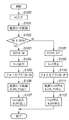
<実施形態1の電源装置の動作手順例>
図3は、実施形態1に係る電源装置の動作を表すフローチャートを示したものである。なお、図3は図2の回路の動作手順を示すものであるが、その一部をソフトウエアのプログラム制御に置き換えることも可能である。
<Operation Procedure Example of Power Supply Device of Embodiment 1>
FIG. 3 is a flowchart illustrating the operation of the power supply device according to the first embodiment. FIG. 3 shows the operation procedure of the circuit of FIG. 2, but a part of it can be replaced by software program control.
まず、ステップS100で商用電源等の交流(AC)供給源から電力を入力し、ステップS101で第1のコンバータ部11−1の電源IC103が起動してスイッチング動作を開始する。
First, power is input from an alternating current (AC) supply source such as a commercial power source in step S100, and in step S101, the
ステップS102でユーザによってSW18がONされれば、ステップS103に進み、FET19をON状態とし、ステップS104にてVcc1が出力される。Vcc1の出力によって、ステップS105にてフォトカプラ128の発光部がON状態となり、受光部のトランジスタがON状態となる。次に、ステップS106にて第2のコンバータ部12−1の電源IC120が起動し、同時にZRX_PSが出力される。次に、ステップS107にてVcc2が出力されつつ、ゼロクロス信号出力部13−1からZRX信号が出力される。
If the
もしステップS102にてSW18がOFF状態となった場合、ステップS108にてFET19がOFF状態となり、ステップS109でVcc1の出力が停止する。次に、ステップS110にてフォトカプラ128がOFFし、ステップS111にて電源IC120が停止して、同時にZRX_PS出力も停止する。そして、ステップS112にてVcc2の出力が停止しつつ、ZRX信号の出力も停止する。これらステップS100からS112のステップは、繰り返し実行されているものとする。
If the
<従来の電源装置の回路構成例>
図4は、本発明の構成と比較するために、従来例の電源装置を表した図である。なお、図2と同様の構成要素は同じ参照番号を付与している。
<Circuit configuration example of a conventional power supply device>
FIG. 4 is a diagram showing a conventional power supply apparatus for comparison with the configuration of the present invention. Components similar to those in FIG. 2 are given the same reference numerals.
本発明と異なる構成として上記特許文献1を例にする。従来例では、ゼロクロス回路における電力消費を低減した構成を、リレー117aおよび117bと、ゼロクロス信号出力部13’として示した。第1のコンバータ部11’の構成は、基本点に第1のコンバータ部11−1と同じである。
The above-mentioned Patent Document 1 is taken as an example as a configuration different from the present invention. In the conventional example, the configuration in which the power consumption in the zero cross circuit is reduced is shown as the
リレー117aおよび117bは、CPU14のDRV信号の出力によって、ゼロクロス信号出力部13’へのACラインからの入力を低消費電力状態では遮断し、電力消費を低減する構成となっている。
The
第2のコンバータ部12’の抵抗134とダイオード135、コンデンサ136は、トランス補助巻き線123cからの電圧出力を平滑化する構成である。
The
ゼロクロス信号出力部13’において、ACラインの電圧がダイオード139で半波整流された電圧は、抵抗140を介してツェナーダイオード143に印加される。そして、フォトカプラ142の発光側素子のON/OFF状態が切り替わることで、ゼロクロス信号ZRXがCPU14に出力される。ACラインの電圧は100V系の商用電源であれば、ダイオード139で半波整流されたピーク電圧は約140Vとなり、フォトカプラ142の発光素子に入力するためには抵抗140とツェナーダイオード143にて電圧を降下させる必要がある。この際、フォトカプラ142の発光側電流を数十ミリアンペアと設定しても数10Vから100V程度降下した電圧との積である電力消費は数Wとなり、無駄な電力消費となる。
In the zero cross
そのため、従来例は、前述したようにリレー117a、117bによって低消費電力状態ではACラインからの入力を遮断し、ゼロクロス信号出力部13’への電力供給を停止する構成となっている。CPU14にて低消費電力状態に遷移する場合でゼロクロス信号ZRXの出力が不要である場合、DRV出力をLow出力にすることで、リレー117bの励磁部RLの通電を停止して、ACラインからの入力を遮断する。ゼロクロス信号ZRXの出力が必要である場合、DRV出力をHigh出力にすることで、リレー117bの励磁部RLに通電して、ACラインからの電圧をゼロクロス信号出力部13’へ入力する。
Therefore, in the conventional example, as described above, the
さらに、複数のコンバータを接続した場合を考慮すると、第2のコンバータ部12’のスイッチングトランス123c補助巻き線からの電力を電源IC120が消費する構成をとる場合がある。補助巻き線123cからの出力を抵抗134とダイオード135、コンデンサ136で平滑化する際に数ワットの電力消費が発生し損失となる。もし複数コンバータの各々のトランス補助巻き線と、出力電圧を平滑化する回路を構成した場合、その合計で無駄な電力消費が発生することとなる。
Furthermore, considering the case where a plurality of converters are connected, the
<実施形態1の効果>
以上述べたように、図2と図3で示した本発明の実施形態1では、コンバータの動作状態および停止状態を切り換えると同時に、ゼロクロス回路の動作状態および停止状態を1系統の制御で切り換えることができる。そのため、複数のコンバータの補助巻き線を削減し、補助巻き線からの出力を整流する際の電力消費を低減することが可能となる。
<Effect of Embodiment 1>
As described above, in the first embodiment of the present invention shown in FIGS. 2 and 3, the operation state and the stop state of the converter are switched at the same time, and the operation state and the stop state of the zero cross circuit are switched by one system control. Can do. Therefore, it is possible to reduce the auxiliary windings of the plurality of converters and reduce the power consumption when rectifying the output from the auxiliary windings.
[実施形態2]
以下に、本発明の実施形態2について、図を参照して説明する。
[Embodiment 2]
Embodiment 2 of the present invention will be described below with reference to the drawings.
<実施形態2の電源装置の回路構成例>
図5は、前述の図2の構成にさらにスイッチ素子と制御信号/CNV2_ONを追加した構成の、本発明の実施形態2の電源装置の回路構成例を示した図である。
<Example of Circuit Configuration of Power Supply Device of Embodiment 2>
FIG. 5 is a diagram showing a circuit configuration example of the power supply device according to the second embodiment of the present invention in which a switch element and a control signal / CNV2_ON are further added to the configuration of FIG.
本実施形態2は、SW18がON状態での、スタンバイモードやスリープモード等の低消費電力状態を考慮したものである。なお、図5で図2と同様の構成要素は同じ参照番号を付与している。図5の第1のコンバータ11−2、ゼロクロス信号出力部13−2は、基本的に図2の第1のコンバータ11−1、ゼロクロス信号出力部13−1と同様である。
The second embodiment takes into consideration low power consumption states such as a standby mode and a sleep mode when the
第2のコンバータ12−2のスイッチ素子133は、CPU14からの/CNV2_ON信号を用いて第2のコンバータ部12−2の動作と、ゼロクロス信号出力部13−2への電力供給を制御する。
The
(/CNV2_ON信号がLow状態の場合)
/CNV2_ON信号がLow状態の場合、スイッチ素子133がON状態となり、フォトカプラ128の発光側素子が通電され、スイッチ素子127がON状態となる。かつ、ゼロクロス信号出力部13−2にゼロクロス信号生成電力ZRX_PSが供給される。また、第1のコンバータ部11−2からのIC Vccが電源IC120に動作電力として供給され、電源IC120が動作し、Vcc2が出力される。
(When / CNV2_ON signal is Low)
When the / CNV2_ON signal is in the low state, the
ダイオード139と抵抗140からのAC電圧の半波がトランジスタ141に供給されて、トランジスタ141が半波ごとにON状態とOFF状態を繰り返す。フォトカプラ142の受光側がON状態とOFF状態を繰り返し、ゼロクロス信号出力部13−2からCPU14にZRX信号が出力される。
A half wave of the AC voltage from the
(/CNV2_ON信号がHigh状態の場合)
/CNV2_ON信号がHigh状態の場合、スイッチ素子133がOFF状態となり、フォトカプラ128の発光側素子の通電が停止し、スイッチ素子127がOFF状態となる。かつ、ゼロクロス信号出力部13−2へのゼロクロス信号生成電力ZRX_PSの供給が停止する。また、第1のコンバータ部11−2からのIC Vccの供給が停止し、電源IC120が停止して、Vcc2の出力が停止する。ダイオード139からのAC電圧の半波が供給されてもフォトカプラ142の受光側はOFF状態となり、ゼロクロス信号出力部13−2からのZRX信号はHigh状態のままとなる。
(When / CNV2_ON signal is High)
When the / CNV2_ON signal is in the high state, the
<実施形態2の電源装置の動作手順例>
図6は、実施形態2に係る電源装置の動作を表すフローチャートを示したものである。なお、図6は図5の回路の動作手順を示すものであるが、その一部をソフトウエアのプログラム制御に置き換えることも可能である。なお、図3と同じ参照番号は、同様の処理を示す。
<Example of Operation Procedure of Power Supply Device of Embodiment 2>
FIG. 6 is a flowchart showing the operation of the power supply device according to the second embodiment. FIG. 6 shows the operation procedure of the circuit of FIG. 5, but part of it can be replaced by software program control. Note that the same reference numerals as those in FIG. 3 indicate similar processes.
ステップS100からS112のステップは、図3で説明した内容と同じである。以下、CPU14が電源装置を含めて負荷の動作状態をスタンバイモードやスリープモード等の低消費電力状態からVcc2を出力する場合を説明する。
Steps S100 to S112 are the same as those described in FIG. Hereinafter, a case where the
ステップS104でVcc1が出力された状態から、ステップS113でCPU14内の処理によって/CNV2_ON出力をLow状態にする。その場合、ステップS114にてスイッチ素子133であるトランジスタがONし、以降のステップでVcc2の出力とZRX信号の出力を開始する。
From the state in which Vcc1 is output in step S104, the / CNV2_ON output is set to the low state by processing in the
もしステップS113でCPU14内の処理によって/CNV2_ON出力をHigh状態にする。その場合、低消費電力状態に遷移するため、ステップS115にてスイッチ素子133であるトランジスタがOFFし、以降のステップでVcc2の出力とZRX信号の出力が停止する。
In step S113, the / CNV2_ON output is set to a high state by processing in the CPU. In that case, in order to shift to the low power consumption state, the transistor which is the
これらステップS100からS115のステップは繰り返し実行されているものとする。 These steps S100 to S115 are repeatedly executed.
<実施形態2の効果>
以上述べたように、図5と図6で示した本発明の実施形態2では、第2のコンバータ部の動作および停止状態を切り換える際と、ゼロクロス回路の動作および停止状態を同時に切り換えることができる。そのため、ゼロクロス回路に入力するゼロクロス信号生成電力の消費を低減することが可能となる。
<Effect of Embodiment 2>
As described above, in the second embodiment of the present invention shown in FIGS. 5 and 6, when the operation and stop state of the second converter section are switched, the operation and stop state of the zero cross circuit can be switched simultaneously. . Therefore, it is possible to reduce the consumption of the zero cross signal generation power input to the zero cross circuit.
[実施形態3]
以下に、本発明の実施形態3について、図を参照して説明する。
[Embodiment 3]
The third embodiment of the present invention will be described below with reference to the drawings.
<実施形態3の電源装置の回路構成例>
図7は、本発明の実施形態3に係る電源装置の回路構成例を示す図である。
<Example of Circuit Configuration of Power Supply Device of
FIG. 7 is a diagram illustrating a circuit configuration example of the power supply device according to the third embodiment of the present invention.
前述の実施形態2の図5で示した構成に、ゼロクロス信号出力部13−3において、トランジスタ141への半波入力選択のためスイッチ素子であるトランジスタ144,145および抵抗等の部品を追加した構成である。ZRX信号を生成するために駆動するトランジスタ141の動作電力を供給もしくは停止することができる構成であり、さらに電力消費を低減することができる構成である。なお、図7の第1のコンバータ11−3、第2のコンバータ12−3は、基本的に図5の第1のコンバータ11−2、第2のコンバータ12−2と同様である。
In the configuration shown in FIG. 5 of the above-described second embodiment, in the zero cross signal output unit 13-3, components such as
(/CNV2_ON信号がLow状態の場合)
/CNV2_ON信号がLow状態の場合、スイッチ素子133がON状態となり、フォトカプラ128の発光側素子が通電され、スイッチ素子127がON状態となる。かつ、ゼロクロス信号出力部13−3にゼロクロス信号生成電力ZRX_PSが供給される。第1のコンバータ部11−3からのIC Vccが電源IC120に動作電力として供給され、電源IC120が動作しVcc2が出力される。また同時に、トランジスタ144,145がON状態となり、ダイオード139と抵抗140からのAC電圧の半波がトランジスタ141に供給されて、トランジスタ141が半波ごとにON状態とOFF状態を繰り返す。フォトカプラ142の受光側がON状態とOFF状態を繰り返し、ゼロクロス信号出力部13−3からCPU14にZRX信号が出力される。
(When / CNV2_ON signal is Low)
When the / CNV2_ON signal is in the low state, the
(/CNV2_ON信号がHigh状態の場合)
/CNV2_ON信号がHigh状態の場合、スイッチ素子133がOFF状態となり、フォトカプラ128の発光側素子の通電が停止し、スイッチ素子127がOFF状態となる。かつ、ゼロクロス信号出力部13−3へのゼロクロス信号生成電力ZRX_PSの供給が停止する。第1のコンバータ部11−3からのIC Vccの供給が停止し、電源IC120が停止して、Vcc2の出力が停止する。また同時に、トランジスタ144,145がOFF状態となり、ダイオード139からのAC電圧の半波が供給されても、半波入力が遮断されてトランジスタ141が駆動しない状態となる。つまり、この状態ではVcc2の出力が停止し、かつZRX信号を生成するスイッチ素子141やトランジスタ144の不要な動作が停止して電力消費を低減することが可能となる。また、ダイオード139と抵抗140による電圧降下によって発生する電力消費を低減することが可能となる。また、従来例のようなメカニカルなリレー117を使用しないので接点寿命の影響を受けずまたリレーコイル117bに電力を消費させることが無くなる。
(When / CNV2_ON signal is High)
When the / CNV2_ON signal is in the high state, the
<実施形態3の電源装置の動作手順例>
図8は、実施形態3に係る電源装置の動作を表すフローチャートを示したものである。なお、図8は図7の回路の動作手順を示すものであるが、その一部をソフトウエアのプログラム制御に置き換えることも可能である。なお、図6と同じ参照番号は、同様の処理を示す。
<Example of Operation Procedure of Power Supply Device of
FIG. 8 is a flowchart illustrating the operation of the power supply device according to the third embodiment. FIG. 8 shows the operation procedure of the circuit of FIG. 7, but part of it can be replaced by software program control. Note that the same reference numerals as those in FIG. 6 indicate similar processes.
ステップS100からステップS115のステップは、前述の実施形態2の図6で説明した内容と同じである。 Steps from step S100 to step S115 are the same as those described in FIG. 6 of the second embodiment.
CPU14が電源装置を含めて負荷の動作状態をスタンバイモードやスリープモード等の低消費電力状態から、Vcc2を出力する場合を説明する。
The case where the
ステップS104でVcc1が出力された状態から、ステップS113でCPU14内の処理によって/CNV2_ON出力をLow状態にする。その場合、ステップS114にてスイッチ素子であるトランジスタ133がONし、ステップS105でフォトカプラ128がONする。そして、ステップS106で電源IC120が起動し、ZRX_PSが出力され、次の、ステップS116にてスイッチ素子であるトランジスタ144,145がON状態となる。トランジスタ144,145がON状態となることで、ACラインからの半波電圧がトランジスタ141に供給され、フォトカプラ142の動作によってZRX信号がCPU14に出力される。
From the state in which Vcc1 is output in step S104, the / CNV2_ON output is set to the low state by processing in the
もしステップS113でCPU14内の処理によって/CNV2_ON出力をHigh状態にする。その場合、低消費電力状態に遷移するため、ステップS115にてスイッチ素子であるトランジスタ133がOFFし、ステップS110で128フォトカプラがOFFする。そして、ステップS111で電源IC120が停止して、ZRX_PSの出力が停止し、次の、ステップS117にてスイッチ素子であるトランジスタ144,145がOFF状態となる。そして、以降のステップでVcc2の出力とZRX信号の出力が停止する。トランジスタ144,145がOFF状態となることで、ACラインからの半波電圧がトランジスタ141に供給されない。そのため、フォトカプラ142の動作を停止することによって、ZRX信号の出力が不要なスタンバイモードやスリープモード等の低消費電力状態で消費電力の低減を行うことができる。
In step S113, the / CNV2_ON output is set to a high state by processing in the CPU. In that case, in order to shift to a low power consumption state, the
これらステップS100からS117のステップは、繰り返し実行されているものとする。 These steps from S100 to S117 are repeatedly executed.
<実施形態3の効果>
以上述べたように、ゼロクロス回路の動作および停止状態を切り換える際に同時に半波電圧の供給を切り換えることができ、ゼロクロス回路に入力する半波電圧を降下させる際の電力消費を低減することが可能となる。
<Effect of
As described above, half-wave voltage supply can be switched at the same time when switching the operation and stop state of the zero-cross circuit, and power consumption when dropping the half-wave voltage input to the zero-cross circuit can be reduced. It becomes.
[実施形態4]
以下に、本発明の実施形態4について、図を参照して説明する。
[Embodiment 4]
<実施形態4の電源装置の回路構成例>
図9は、本発明の実施形態3に係る電源装置の回路構成例を示す図である。
<Example of Circuit Configuration of Power Supply Device of
FIG. 9 is a diagram illustrating a circuit configuration example of the power supply device according to the third embodiment of the present invention.
前述の実施形態3で示した図7の構成で、スイッチ素子であるトランジスタ144,145および抵抗等の部品を、フォトリレー146および抵抗で置き換えた構成である。ZRX信号を生成するために駆動するトランジスタ141の動作電力を供給もしくは停止することができる構成である。従って、前述した従来例のようにCPU14からの制御端子であるDRV出力を別途設けることなく、/CNV2_ON出力を用いて13ゼロクロス信号出力部での電力消費を低減することができる構成である。なお、図9の第1のコンバータ11−4、ゼロクロス信号出力部13−4は、基本的に図7の第1のコンバータ11−3、ゼロクロス信号出力部13−3と同様である。
In the configuration of FIG. 7 shown in the above-described third embodiment, the components such as the
(/CNV2_ON信号がLow状態の場合)
/CNV2_ON信号がLow状態の場合、スイッチ素子133がON状態となり、フォトカプラ128の発光側素子が通電され、スイッチ素子127がON状態となる。かつ、13ゼロクロス信号出力部13−4にゼロクロス信号生成電力ZRX_PSが供給される。第1のコンバータ部11−4からのIC Vccが電源IC120に動作電力として供給され、電源IC120が動作し、Vcc2が出力される。また同時に、スイッチ素子133がON状態となることでVcc1がフォトリレー146に供給されてON状態となる。そして、ダイオード139と抵抗140からのAC電圧の半波がトランジスタ141に供給されて、トランジスタ141が半波ごとにON状態とOFF状態を繰り返す。フォトカプラ142の受光側がON状態とOFF状態を繰り返し、ゼロクロス信号出力部13−4からCPU14にZRX信号が出力される。
(When / CNV2_ON signal is Low)
When the / CNV2_ON signal is in the low state, the
(/CNV2_ON信号がHigh状態の場合)
/CNV2_ON信号がHigh状態の場合、スイッチ素子133がOFF状態となり、フォトカプラ128の発光側素子の通電が停止し、スイッチ素子127がOFF状態となる。かつ、ゼロクロス信号出力部13−4へのゼロクロス信号生成電力ZRX_PSの供給が停止する。第1のコンバータ部11−4からのIC Vccの供給が停止し、電源IC120が停止して、Vcc2の出力が停止する。また同時に、Vcc1の供給が停止してフォトリレー146がOFF状態となり、ダイオード139からのAC電圧の半波が供給されてもトランジスタ141が駆動しない状態となる。
(When / CNV2_ON signal is High)
When the / CNV2_ON signal is in the high state, the
<実施形態4の効果>
つまり、この状態ではVcc2の出力が停止し、かつZRX信号を生成するスイッチ素子であるトランジスタ141の不要な動作が停止して電力消費を低減することが可能となる。また、ダイオード139と抵抗140による電圧降下によって発生する電力消費を低減することが可能となる。また、フォトリレー146のようなスイッチ素子を用いることで、図4で示した従来例のような機械式接点を有するリレーより劣化が少なく、長寿命化を図ることが可能となる。
<Effect of
That is, in this state, the output of Vcc2 is stopped, and unnecessary operation of the
10…整流部
11…第1のコンバータ部(CNV1)
12…第2のコンバータ部(CNV2)
13…ゼロクロス信号出力部
14…中央演算処理ユニット(CPU)
15…AC負荷
16、17…DC負荷
18…スイッチ(SW)
100…交流供給源
101…ブリッジ整流回路
102…平滑用コンデンサ
103、120…電源IC
104、121…スイッチング素子
106、123…スイッチングトランス
112、129、128、142…フォトカプラ
141、144、145…スイッチ素子
146…スイッチ素子(フォトリレー)
DESCRIPTION OF
12 ... 2nd converter part (CNV2)
13 ... Zero cross
15 ...
DESCRIPTION OF
104, 121 ... switching
Claims (6)
一次側に主巻線を有し、二次側に出力巻線を有し、前記整流及び平滑した電圧が当該主巻線に印加される第二トランスと、前記第一トランスの補助巻線に誘起された電圧が供給され、かつ、前記第二トランスの主巻線にパルス電圧を印加するために、前記第二トランスの主巻線に接続されたスイッチング素子のスイッチング動作を制御する第二制御部と、を有し、前記第二トランスの出力巻線から第二電圧を出力する第二コンバータと、
前記第一トランスの補助巻線に誘起された電圧が供給され、かつ、入力される前記交流電圧のゼロクロスタイミングに応じたゼロクロス信号を出力するゼロクロス信号出力部と、を備え、
前記第二コンバータは、前記第一電圧の負荷への供給を停止したことに応じて、前記第一トランスの補助巻線に誘起された電圧の前記第二制御部への供給を停止し、かつ、前記第一トランスの補助巻線に誘起された電圧の前記ゼロクロス信号出力部への供給を停止するための切換部を備えたことを特徴とする電源装置。 A first transformer having a main winding and an auxiliary winding on the primary side, an output winding on the secondary side, and a voltage obtained by rectifying and smoothing an input AC voltage applied to the main winding; A first controller for controlling a switching operation of a switching element connected to the main winding of the first transformer in order to apply a pulse voltage to the main winding of the first transformer. A first converter that outputs a first voltage from the output winding of the transformer;
A primary winding is provided on the primary side, an output winding is provided on the secondary side, and the rectified and smoothed voltage is applied to the main winding and the auxiliary winding of the first transformer. A second control for controlling a switching operation of a switching element connected to the main winding of the second transformer in order to supply an induced voltage and apply a pulse voltage to the main winding of the second transformer; A second converter that outputs a second voltage from the output winding of the second transformer,
A zero-cross signal output unit that outputs a zero-cross signal according to a zero-cross timing of the alternating voltage that is supplied with the voltage induced in the auxiliary winding of the first transformer and that is input;
The second converter stops supplying the voltage induced in the auxiliary winding of the first transformer to the second control unit in response to stopping the supply of the first voltage to the load; and A power supply apparatus comprising: a switching unit for stopping supply of the voltage induced in the auxiliary winding of the first transformer to the zero cross signal output unit .
前記画像形成手段を駆動する駆動手段と、
前記画像形成手段と前記駆動手段に電力を供給する電源と、を有し、
前記電源は、
一次側に主巻線と補助巻線を有し、二次側に出力巻線を有し、入力される交流電圧を整流及び平滑した電圧が当該主巻線に印加される第一トランスと、前記第一トランスの主巻線にパルス電圧を印加するために、前記第一トランスの主巻線に接続されたスイッチング素子のスイッチング動作を制御する第一制御部と、を有し、前記第一トランスの出力巻線から第一電圧を出力する第一コンバータと、
一次側に主巻線を有し、二次側に出力巻線を有し、前記整流及び平滑した電圧が当該主巻線に印加される第二トランスと、前記第一トランスの補助巻線に誘起された電圧が供給され、かつ、前記第二トランスの主巻線にパルス電圧を印加するために、前記第二トランスの主巻線に接続されたスイッチング素子のスイッチング動作を制御する第二制御部と、を有し、前記第二トランスの出力巻線から第二電圧を出力する第二コンバータと、
前記第一トランスの補助巻線に誘起された電圧が供給され、かつ、入力される前記交流電圧のゼロクロスタイミングに応じたゼロクロス信号を出力するゼロクロス信号出力部と、を備え、
前記第二コンバータは、前記第一電圧の負荷への供給を停止したことに応じて、前記第一トランスの補助巻線に誘起された電圧の前記第二制御部への供給を停止し、かつ、前記第一トランスの補助巻線に誘起された電圧の前記ゼロクロス信号出力部への供給を停止するための切換部を備えたことを特徴とする画像形成装置。 An image forming means for forming an image;
Driving means for driving the image forming means;
A power source for supplying power to the image forming unit and the driving unit,
The power supply is
A first transformer having a main winding and an auxiliary winding on the primary side, an output winding on the secondary side, and a voltage obtained by rectifying and smoothing an input AC voltage applied to the main winding; A first controller for controlling a switching operation of a switching element connected to the main winding of the first transformer in order to apply a pulse voltage to the main winding of the first transformer. A first converter that outputs a first voltage from the output winding of the transformer;
A primary winding is provided on the primary side, an output winding is provided on the secondary side, and the rectified and smoothed voltage is applied to the main winding and the auxiliary winding of the first transformer. A second control for controlling a switching operation of a switching element connected to the main winding of the second transformer in order to supply an induced voltage and apply a pulse voltage to the main winding of the second transformer; A second converter that outputs a second voltage from the output winding of the second transformer,
A zero-cross signal output unit that outputs a zero-cross signal according to a zero-cross timing of the alternating voltage that is supplied with the voltage induced in the auxiliary winding of the first transformer and that is input;
The second converter stops supplying the voltage induced in the auxiliary winding of the first transformer to the second control unit in response to stopping the supply of the first voltage to the load; and An image forming apparatus comprising: a switching unit for stopping the supply of the voltage induced in the auxiliary winding of the first transformer to the zero cross signal output unit .
Priority Applications (2)
| Application Number | Priority Date | Filing Date | Title |
|---|---|---|---|
| JP2009020738A JP5424663B2 (en) | 2009-01-30 | 2009-01-30 | Power supply device and image forming apparatus |
| US12/690,485 US8830703B2 (en) | 2009-01-30 | 2010-01-20 | Power supply apparatus having plural converters and a zero crossing signal output unit |
Applications Claiming Priority (1)
| Application Number | Priority Date | Filing Date | Title |
|---|---|---|---|
| JP2009020738A JP5424663B2 (en) | 2009-01-30 | 2009-01-30 | Power supply device and image forming apparatus |
Publications (3)
| Publication Number | Publication Date |
|---|---|
| JP2010178573A JP2010178573A (en) | 2010-08-12 |
| JP2010178573A5 JP2010178573A5 (en) | 2012-03-15 |
| JP5424663B2 true JP5424663B2 (en) | 2014-02-26 |
Family
ID=42397569
Family Applications (1)
| Application Number | Title | Priority Date | Filing Date |
|---|---|---|---|
| JP2009020738A Active JP5424663B2 (en) | 2009-01-30 | 2009-01-30 | Power supply device and image forming apparatus |
Country Status (2)
| Country | Link |
|---|---|
| US (1) | US8830703B2 (en) |
| JP (1) | JP5424663B2 (en) |
Families Citing this family (9)
| Publication number | Priority date | Publication date | Assignee | Title |
|---|---|---|---|---|
| JP4678699B2 (en) * | 2009-09-29 | 2011-04-27 | シャープ株式会社 | Motor control device |
| JP5729990B2 (en) * | 2010-11-30 | 2015-06-03 | キヤノン株式会社 | Switching power supply device and image forming apparatus provided with switching power supply device |
| EP2624422B1 (en) * | 2012-01-31 | 2019-08-28 | Canon Kabushiki Kaisha | Power source, power failure detection apparatus, and image forming apparatus |
| JP6608197B2 (en) | 2015-06-30 | 2019-11-20 | キヤノン株式会社 | Power supply device and image forming apparatus having power supply device |
| KR102283082B1 (en) * | 2015-11-09 | 2021-07-30 | 삼성전기주식회사 | Power supplying apparatus |
| JP6824708B2 (en) | 2016-11-24 | 2021-02-03 | キヤノン株式会社 | Power supply device and image forming device |
| KR20200029196A (en) | 2018-09-10 | 2020-03-18 | 휴렛-팩커드 디벨롭먼트 컴퍼니, 엘.피. | Power supply device to output zero-cross information of half ac wave |
| JP2020188615A (en) | 2019-05-16 | 2020-11-19 | キヤノン株式会社 | Power supply device and image forming apparatus |
| CN111478563B (en) * | 2020-05-15 | 2023-03-24 | 电子科技大学 | Zero-crossing detection circuit suitable for BUCK converter |
Family Cites Families (8)
| Publication number | Priority date | Publication date | Assignee | Title |
|---|---|---|---|---|
| US5173846A (en) * | 1991-03-13 | 1992-12-22 | Astec International Ltd. | Zero voltage switching power converter |
| US5745358A (en) * | 1996-05-01 | 1998-04-28 | Compaq Computer Corporation | Variable-frequency converter with constant programmed delay |
| JP2003199336A (en) | 2001-12-25 | 2003-07-11 | Sharp Corp | Power supply and image forming device |
| KR100986762B1 (en) * | 2003-09-08 | 2010-10-08 | 페어차일드코리아반도체 주식회사 | Switching power supply apparatus and power supply method thereof |
| GB2438463A (en) * | 2006-05-23 | 2007-11-28 | Cambridge Semiconductor Ltd | Regulating the output of a switch mode power supply |
| WO2007135453A2 (en) * | 2006-05-23 | 2007-11-29 | Cambridge Semiconductor Limited | Switch mode power supply controllers |
| JP2008172914A (en) * | 2007-01-11 | 2008-07-24 | Canon Inc | Power supply device and image forming device |
| JP5203643B2 (en) * | 2007-07-04 | 2013-06-05 | キヤノン株式会社 | Zero cross detection circuit, zero cross signal output circuit and power supply |
-
2009
- 2009-01-30 JP JP2009020738A patent/JP5424663B2/en active Active
-
2010
- 2010-01-20 US US12/690,485 patent/US8830703B2/en active Active
Also Published As
| Publication number | Publication date |
|---|---|
| US20100195352A1 (en) | 2010-08-05 |
| JP2010178573A (en) | 2010-08-12 |
| US8830703B2 (en) | 2014-09-09 |
Similar Documents
| Publication | Publication Date | Title |
|---|---|---|
| JP5424663B2 (en) | Power supply device and image forming apparatus | |
| US6845018B2 (en) | Power circuit and method for controlling drive and control voltages of an image formation apparatus | |
| JP6304577B2 (en) | Power supply system, image forming apparatus equipped with the same power supply system, and control method of power supply system | |
| US20070097715A1 (en) | Switching mode power supply and a method of operating the power supply in a power save mode | |
| JP4965939B2 (en) | Power supply | |
| KR100268465B1 (en) | Initial drive voltage supply circuit for switching mode power supply | |
| US20120250365A1 (en) | Switching power supply | |
| US8634214B2 (en) | Current resonance power supply with AC input detection into the primary winding | |
| JP2008172914A (en) | Power supply device and image forming device | |
| JP2015171289A (en) | Power supply controller | |
| EP3698456B1 (en) | Ac/dc converter, luminaire and method providing an improved start-up circuit | |
| JP7421341B2 (en) | Power supply and image forming device | |
| JP2004120826A (en) | Switching power supply, image forming apparatus, and method of reducing power consumption | |
| JP2001005350A (en) | Image recorder and control method therefor | |
| JP2007174727A (en) | Synchronous rectifying circuit | |
| JP2018126037A (en) | Power supply device and electrical equipment | |
| JP6635681B2 (en) | Image forming device | |
| JP2006101597A (en) | Power supply circuit | |
| JP2004328837A (en) | Switching power supply circuit and switching regulator comprising the same | |
| JP2007047368A (en) | Image forming apparatus | |
| JP2006287429A (en) | Image forming apparatus | |
| JP4657137B2 (en) | Switching power supply | |
| KR100840638B1 (en) | Multi output switching power circuit for reducing power consumption in a standby mode | |
| JP6453090B2 (en) | Image forming apparatus | |
| JP7214472B2 (en) | Power supply and image forming apparatus |
Legal Events
| Date | Code | Title | Description |
|---|---|---|---|
| A521 | Written amendment |
Free format text: JAPANESE INTERMEDIATE CODE: A523 Effective date: 20120127 |
|
| A621 | Written request for application examination |
Free format text: JAPANESE INTERMEDIATE CODE: A621 Effective date: 20120127 |
|
| A977 | Report on retrieval |
Free format text: JAPANESE INTERMEDIATE CODE: A971007 Effective date: 20130424 |
|
| A131 | Notification of reasons for refusal |
Free format text: JAPANESE INTERMEDIATE CODE: A131 Effective date: 20130426 |
|
| A521 | Written amendment |
Free format text: JAPANESE INTERMEDIATE CODE: A523 Effective date: 20130624 |
|
| TRDD | Decision of grant or rejection written | ||
| A01 | Written decision to grant a patent or to grant a registration (utility model) |
Free format text: JAPANESE INTERMEDIATE CODE: A01 Effective date: 20131028 |
|
| A61 | First payment of annual fees (during grant procedure) |
Free format text: JAPANESE INTERMEDIATE CODE: A61 Effective date: 20131126 |
|
| R151 | Written notification of patent or utility model registration |
Ref document number: 5424663 Country of ref document: JP Free format text: JAPANESE INTERMEDIATE CODE: R151 |