JP5372618B2 - Patterned substrate inspection apparatus and patterned substrate inspection method - Google Patents
Patterned substrate inspection apparatus and patterned substrate inspection method Download PDFInfo
- Publication number
- JP5372618B2 JP5372618B2 JP2009154536A JP2009154536A JP5372618B2 JP 5372618 B2 JP5372618 B2 JP 5372618B2 JP 2009154536 A JP2009154536 A JP 2009154536A JP 2009154536 A JP2009154536 A JP 2009154536A JP 5372618 B2 JP5372618 B2 JP 5372618B2
- Authority
- JP
- Japan
- Prior art keywords
- inspection
- pattern
- light
- area
- inspection area
- Prior art date
- Legal status (The legal status is an assumption and is not a legal conclusion. Google has not performed a legal analysis and makes no representation as to the accuracy of the status listed.)
- Expired - Fee Related
Links
Images


Description
本発明は、パターン付き基板検査装置およびパターン付き基板検査方法に関し、例えば、半導体製造工程やフラットパネルデイスプレイの製造工程に代表される薄膜プロセスを経て基板(例えば、半導体ウェーハやガラス基板)上に形成された微細パターンの欠陥や異物などの検出を行う装置および検査方法に関するものである。 The present invention relates to a patterned substrate inspection apparatus and a patterned substrate inspection method, for example, formed on a substrate (for example, a semiconductor wafer or a glass substrate) through a thin film process typified by a semiconductor manufacturing process or a flat panel display manufacturing process. The present invention relates to an apparatus and an inspection method for detecting a defect or a foreign matter of a fine pattern.
従来のパターン付き基板検査装置として、例えば特開昭62−70739号公報がある。すなわち、正常パターン部からの散乱光の影響による欠陥の誤検出を抑えるために、照明光はS偏光ビームであり受光部分はP偏光のみ検出する検光機能を備えた検査装置である。これにより、本当に検出が必要である異物のみを高感度で検出することを可能にしている。 As a conventional substrate inspection apparatus with a pattern, for example, there is JP-A-62-270739. In other words, in order to suppress the erroneous detection of defects due to the influence of scattered light from the normal pattern portion, the inspection device is equipped with a light detection function for detecting only the P-polarized light in the light receiving portion and the light receiving portion. This makes it possible to detect with high sensitivity only foreign matters that really need to be detected.
しかしながら、上記従来技術では、かえって欠陥の誤検出が増えることがあることを発明者は確認した。例えばメモリ製品のウェーハでは、情報を記録するメモリセル部では検光機能により正常パターン部からの散乱光の影響による欠陥の誤検出を抑えることができるが、I/O部などの大きなパターン部では検光機能により正常パターン部からの散乱光の影響による欠陥の誤検出を抑えることができず、検出が必要である欠陥の検出のみを行うことができないという課題がある。 However, the inventor has confirmed that in the above-described prior art, erroneous detection of defects may increase. For example, in a memory product wafer, in the memory cell portion for recording information, the detection function can suppress erroneous detection of defects due to the influence of scattered light from the normal pattern portion, but in a large pattern portion such as an I / O portion. There is a problem that the detection function cannot suppress erroneous detection of defects due to the influence of scattered light from the normal pattern portion, and cannot detect only the defects that need to be detected.
本発明の一つの目的は、検光機能が正常パターン部からの散乱光の影響による欠陥の誤検出を抑えることができるエリアと、抑えることができない領域を弁別し、この2つの領域を違う検査方法で検査することにより、本当に検出が必要である欠陥のみを高感度で検出することを可能にしたパターン付き基板検査装置又はパターン付き基板検査方法を提供することにある。 One object of the present invention is to discriminate between an area where the detection function can suppress erroneous detection of defects due to the influence of scattered light from the normal pattern portion and an area where the detection cannot be suppressed, and the two areas are inspected differently. It is an object of the present invention to provide a patterned substrate inspection apparatus or a patterned substrate inspection method that can detect only defects that really need to be detected with high sensitivity.
上記目的を達成するための、本発明の一つの特徴は、ステージ上に載せられた被検査物表面上に所望の光束で斜方照明する照明系と、照明系によって照明された個所から発生する任意の方向に反射する散乱光を集光する集光光学系と、前記集光光学系で集光された散乱光を受光して輝度信号に変換する光電変換手段を有する検出光学系と、前記検出光学系で検出された輝度信号に基づいて前記被検査物上の欠陥を検出する判定部とを備えたパターン付き基板検査装置において、正常パターン部からの散乱光の影響による欠陥の誤検出を抑えるために、前記照明系はS偏光ビームであり、前記検出光学系はP偏光のみ検出する検光機能を備え、検査エリアを、前記検光機能が正常パターン部からの散乱光の影響による欠陥の誤検出を抑えることができるエリアと、抑えることができない領域に弁別し、この2つの領域を違う検査処理で検査を行うことにある。 To achieve the above object, one feature of the present invention is generated from an illumination system that illuminates obliquely with a desired light beam on a surface of an object to be inspected placed on a stage, and a portion illuminated by the illumination system. A condensing optical system for condensing scattered light reflected in an arbitrary direction; a detection optical system having photoelectric conversion means for receiving the scattered light collected by the condensing optical system and converting it into a luminance signal; and In a substrate inspection apparatus with a pattern including a determination unit that detects a defect on the inspection object based on a luminance signal detected by a detection optical system, erroneous detection of a defect due to an influence of scattered light from a normal pattern unit In order to suppress, the illumination system is an S-polarized beam, the detection optical system has a light detection function for detecting only P-polarized light, and the inspection area has a defect due to the influence of scattered light from a normal pattern portion. To reduce false positives An area as possible, to discriminate the region can not be suppressed, in carrying out the inspection in the inspection process differently the two regions.
ここで欠陥の誤検出が抑えられる検査エリアとは、照明光の波長以下のパターン幅を有するパターンであるメモリセル部と、パターンの無いベア部である。また、欠陥の誤検出が抑えられない検査エリアとは、照明光の波長より大きなパターン幅を有するパターン部のエッジ部分である。 Here, the inspection area in which erroneous detection of defects is suppressed includes a memory cell portion which is a pattern having a pattern width equal to or smaller than the wavelength of illumination light, and a bare portion having no pattern. The inspection area in which erroneous detection of defects cannot be suppressed is an edge portion of a pattern portion having a pattern width larger than the wavelength of illumination light.
本発明の一つの態様によれば、パターン付きウェーハ検査装置において、本当に検出が必要である異物やショートなどのパターン欠陥を高感度で検出することが可能である。 According to one aspect of the present invention, in a patterned wafer inspection apparatus, it is possible to detect with high sensitivity a pattern defect such as a foreign substance or a short that really needs to be detected.
本発明に係わるパターン付きウェーハ検査装置の実施形態について図面を用いて説明する。 An embodiment of a patterned wafer inspection apparatus according to the present invention will be described with reference to the drawings.
まず、図1に実施の形態を実現するためのパターン付きウェーハ検査装置の実施例を示す。位置座標が測定されてXY方向に走行制御されるステージ114上に載せられる被検査物であるウェーハ113と、例えば波長488nmのArレーザーをS偏光に偏波させた光源からなる光源102、反射ミラー103により構成される斜方照明光学系101と、照明光104をウェーハ113へ照明し、ウェーハ113から反射される散乱光を集光する集光レンズ106と、フォトマル,CCDカメラ,CCDセンサ、及びTDIセンサ等の少なくとも一つから構成され受光された散乱光はアナログ輝度信号に変換する光電変換器108,ウェーハ113から反射される散乱光中,P偏光の成分のみを透過する偏光板107により構成される検出光学系105と、光電変換器108から出力されるアナログ輝度信号をデジタル輝度信号に変換するA/D変換部109と、上記ステージ114から測定される位置座標を基に上記ステージ114を走行制御するステージコントローラ112と、ステージ114の走行に同期して欠陥部を検出しその輝度信号を算出する判定部110と、上記ステージコントローラ112を制御し、さらに判定部110を制御し判定部110から得られる検査結果を受ける全体制御部111とから構成される。
First, FIG. 1 shows an example of a wafer inspection apparatus with a pattern for realizing the embodiment. A
判定部110としては、例えばステージ114の走行に同期してスキャンする光電変換器108のスキャンクロックに同期したパイプライン処理を行える専用のデジタル信号回路などを用いることができる。
As the
判定部110の処理方法として上記のように同期処理を行わず、例えば一旦A/D変換部109の出力をメモリに記憶し、非同期で処理する方法もある。非同期で処理する場合は、一般的には検査速度は遅いが、専用の信号処理回路を必要とせず、回路規模を小さくできる。また、図示しないが、判定部110の内部または検査装置内に、経験値としての過去データを記憶する登録部を有しても良い。
As a processing method of the
次に、このような検査装置のA/D変換部109で処理される信号を、判定部110で2次元に配列した画像とした場合、どのように見えるのか述べる。
Next, it will be described how the signal processed by the A /
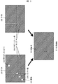
図2上側のBFイメージ(明視野画像)は、通常メモリ製品のウェーハ回路パターンがどのように明視野顕微鏡で見えるか示したものである。回路パターンはおおよそ、以下の3つの部分に分かれる。すなわち、光源102の波長以下のパターン幅のパターンを有するメモリセル部のL/S(ライン アンド スペース)パターン204,光源102の波長よりも大きなパターン幅のパターンを有するパターン部205、何もパターンが無いベア部206である。メモリセル部のL/Sパターン204は情報を記録するビット部分などである。大きなパターン部205は、メモリアドレスなどを制御するI/O部分などである。ベア部206は、何も回路が形成されていない部分である。
The BF image (bright field image) on the upper side of FIG. 2 shows how a wafer circuit pattern of a normal memory product can be seen with a bright field microscope. The circuit pattern is roughly divided into the following three parts. That is, an L / S (line and space) pattern 204 of a memory cell portion having a pattern width pattern equal to or smaller than the wavelength of the
このような回路パターンをパターン付き基板検査装置の判定部110で2次元に配列した暗視野画像を図2下側のDFイメージとして示す。メモリセル部のL/Sパターン204は、L/Sのピッチが光源102の波長以下であることが多く、その場合は真っ暗に見える。光源102の波長よりも大きなパターン幅のパターンを有するパターン部205は、そのエッジやエルボー部が明るく見える。パターンの無いベア部206は真っ暗に見える。またメモリセル部のL/Sパターン204上にある異物またはショート201は明るい輝点として見える。この異物またはショート201は検出が必要であるとされる欠陥である。ヒロックまたはグレイン202は検出してしまうと検出の誤検出であると判定されてしまうパターンであるが、検出光学系105の検光機能により光らない。ベア部206上にある異物203は明るい輝点として見える。
A dark field image in which such a circuit pattern is two-dimensionally arranged by the
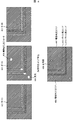
図3に、上記の様に見える検査対象であるウェーハ上の第一ダイの回路パターンのDFイメージを、同一ウェーハ上における隣の第二ダイにおける対応する回路パターンのDFイメージと比較して、差分を抽出し、ある輝度以上の差分が残れば判定部110で欠陥と判定する様子を実施例の比較例として示す。
FIG. 3 compares the DF image of the circuit pattern of the first die on the wafer to be inspected as seen above with the DF image of the corresponding circuit pattern on the adjacent second die on the same wafer. As a comparative example of the embodiment, a state in which the
図3に示すように、上記第一ダイに相当するダイA301の大きなパターン部エッジ306のDFイメージ(図3上左部参照)と、上記第二ダイに相当するダイB302の大きなパターン部エッジ306のDFイメージ(図3上右部参照)では輝度の差が出る。BFイメージでは少しの差異であって、欠陥検出が必要とされない部分であっても、散乱光で見るDFイメージでは大きな差となるからである。この傾向は、検出光学系105の検光機能により、光源102の波長よりもパターン幅のパターンを有する大きなパターン部エッジ306の90°角のエルボー部307でさらに大きくなることを発明者は確認した。これにより差画像303(図3下部参照)を計算し、設定閾値よりも大きい部分を欠陥と判定すると、本来検出したい異物またはショート304や異物305だけではなく、光源102の波長よりも大きなパターン部エッジ306の一部分であるエルボー部307を誤検出してしまう。これが、比較例の技術において、かえって欠陥の誤検出が増えることがある理由である。
As shown in FIG. 3, a DF image (see the upper left portion of FIG. 3) of the large pattern portion edge 306 of the die A301 corresponding to the first die and a large pattern portion edge 306 of the die B302 corresponding to the second die. In the DF image (see the upper right part in FIG. 3), a difference in luminance appears. This is because there is a slight difference in the BF image, and even in a portion where the defect detection is not required, a large difference is caused in the DF image viewed with scattered light. The inventor has confirmed that this tendency is further increased by the elbow portion 307 having a 90 ° angle of the large pattern portion edge 306 having a pattern having a pattern width larger than the wavelength of the
そこで、発明者は、光源102の波長以下のパターン幅のパターンを有するパターンであるメモリセル部のL/S(ライン アンド スペース)パターン204や、パターンの無いベア部206のように、ヒロックまたはグレイン202のような誤検出が抑えられる検査エリアと、光源102の波長よりも大きなパターン部エッジ306のように、エルボー部307のような欠陥の誤検出が抑えられない検査エリアを弁別し、この2つのエリアを違う検査方法で検査を行う技術を発明した。その一例を図4と図5を用いて説明する。
Therefore, the inventor uses hillocks or grains such as the L / S (line and space) pattern 204 of the memory cell portion which is a pattern having a pattern width equal to or smaller than the wavelength of the
図4のダイA401は検査ダイであり、ダイB402は右隣のダイ、ダイC403は左隣のダイの同じ回路パターン部を示す。3つのダイ中、同じピクセルに着目し2つ以上のダイで暗い部分であれば、輝度判定エリア407,408とする。この時、判定基準となる暗さは、おおよそ光電変換器108を遮光した場合の暗さに数階調のマージンを持たせた値以下である。一般的には2〜3階調のマージンであり、ノイズが多い検査対象の場合は5〜6階調のマージンのように、マージンを幅広くすることが望ましい。それ以外の暗くない部分はダイ比較エリア409,410とする。この処理の様子を図5のフローの処理501〜処理503に示す。
A die A401 in FIG. 4 is an inspection die, a die B402 is the right adjacent die, and a die C403 is the same circuit pattern portion of the left adjacent die. Focusing on the same pixel among the three dies, if two or more dies are dark portions, they are set as luminance determination areas 407 and 408. At this time, the darkness that is the determination criterion is approximately equal to or less than a value obtained by adding a margin of several gradations to the darkness when the
輝度判定エリア407,408では、例えばダイA401の画像で設定閾値X以上の部分を欠陥と判定する。この様子を図5のフローの処理505に示す。
In the luminance determination areas 407 and 408, for example, a portion of the image of the die A401 that is equal to or greater than the set threshold value X is determined as a defect. This state is shown in the
また、ダイ比較エリア409,410では、例えば差画像406の画像で設定閾値Y以上の部分を欠陥と判定する。設定閾値X,Yは、経験値として予め装置に登録されていても良いし、検査毎に設定されなおしても良い。設定閾値X,Yは検査対象に応じて決定される。 Further, in the die comparison areas 409 and 410, for example, a portion of the difference image 406 that is equal to or larger than the set threshold Y is determined as a defect. The setting threshold values X and Y may be registered in advance in the apparatus as experience values, or may be reset for each examination. The set threshold values X and Y are determined according to the inspection object.
こうして、輝度判定エリア407,408とダイ比較エリア409,410とで別々の欠陥判定閾値を設定できるため、本当に検出が必要な欠陥のみを高感度で検出することが可能となる。この判定を、検査ダイAの全てのピクセルで実行する。この様子を図5の処理506〜処理507に示す。
In this way, since different defect determination thresholds can be set for the luminance determination areas 407 and 408 and the die comparison areas 409 and 410, only defects that really need to be detected can be detected with high sensitivity. This determination is performed on all the pixels of the inspection die A. This state is shown in
以上のように、図5は検査装置の欠陥検出フローの一例であり、その内容は次の通りである。すなわち、図5の処理がスタート(START)すると、検査ダイAと右隣ダイBと左隣ダイCとの各画像の対応する同じ位置のピクセル(またはエリア)の画像データの読み込み処理501,読み込んだ画像に基づき、そのピクセル(またはエリア)が3ダイとも暗ければ、そのピクセル(またはエリア)を「輝度判定エリア」と判定する処理502,輝度判定エリアか否か判定する処理503,輝度判定エリアならば(YES)輝度判定エリアの閾値XとダイA画像の該当箇所の輝度を比較し、該当箇所の輝度が大ならば欠陥と判定する処理505,輝度判定エリアでないならば(NO)ダイ比較エリアの閾値Yと差画像の該当箇所の輝度を比較し、該当箇所の輝度が大ならば欠陥と判定する処理504,全てのピクセル(または予め検査対象としている所定のピクセル)において欠陥判定が終了したか否か判定する506,終了していない場合(NO)は、次のピクセル(またはエリア)の判定を俗効する処理507から処理501へ戻り、欠陥判定終了ならば(YES)、図5の処理が終了する(END)。
As described above, FIG. 5 is an example of a defect detection flow of the inspection apparatus, and the contents thereof are as follows. That is, when the process of FIG. 5 is started (START), image
図4と図5の例では、検査ダイと左右両隣の3ダイを使用した場合の例を説明したが、検査ダイを含む、任意の3ダイを用いても良い。また3つのダイ中、同じピクセルに着目し2つのダイ以上で暗い部分であれば、輝度判定エリア407,408と判定したが、任意のM個のダイ中、N個以上のダイで暗い部分であれば、輝度判定エリア407,408と判定してもよい。ここでNはMよりも小さい整数である。一般には、N=M−1であるが、NがMより2以上小さい場合もある。 In the examples of FIGS. 4 and 5, the example in which the inspection die and the three right and left adjacent dies are used has been described, but any three dies including the inspection die may be used. Also, in the three dies, if it is a dark part with two or more dies paying attention to the same pixel, it is determined as the luminance judgment areas 407 and 408. However, in any M dies, N or more dies are dark parts. If there are, the luminance determination areas 407 and 408 may be determined. Here, N is an integer smaller than M. In general, N = M−1, but N may be two or more smaller than M.
次に、図4と図5の実施例において、装置を操作するオペレータの操作と検査処理が、どのようなものであるか、その一例を図6と図7を用いて説明する。 Next, an example of the operation of the operator who operates the apparatus and the inspection process in the embodiments of FIGS. 4 and 5 will be described with reference to FIGS.
まず、図6の検査条件設定画面603において、検査モード601を設定する。設定閾値X,Yが予め装置に登録されていれば、「誤検出消去モード」などと設定する。この検査フローの様子を図7の処理701に示す。
First, the
次に、検査スタートボタン602を押す。装置はウェーハの検査スキャンを初め、図5のフローに従い、自動的にウェーハの検査を行い、全てのダイの検査を終了し、ウェーハの検査を終了する。この様子を図7の処理702〜処理705に示す。
Next, the
以上のように、図7は検査装置の検査フローの一例であり、その内容は次の通りである。すなわち、図7の処理がスタート(START)すると、検査設定画面に検査モードを入力する処理701,検査スタートボタンを押す処理702,検査対象であるウェーハの検査のためのスキャンを実行する処理703,図5で示される処理フローに従ってパターン付き基板検査装置の判定部が欠陥判定を行う処理704,ウェーハの検査終了する処理705を経て、図7の処理が終了する(END)。
As described above, FIG. 7 is an example of the inspection flow of the inspection apparatus, and the contents thereof are as follows. That is, when the process of FIG. 7 is started (START), a
以上によれば、オペレータは、検査エリアの設定などを行う必要が無く、その手間に煩わされることが無い。 According to the above, the operator does not need to set an inspection area or the like, and is not bothered by the trouble.
また、以上述べたように、検査エリアを、検光機能が欠陥の誤検出を抑えられる領域と、抑えることができない領域に弁別し、この2つの領域を違う検査処理で検査を行うことにより、本当に検出が必要である欠陥のみを高感度で検出することが可能である。 In addition, as described above, the inspection area is discriminated into an area where the light detection function can suppress erroneous detection of defects and an area where the detection cannot be suppressed, and the two areas are inspected by different inspection processes. Only defects that really need to be detected can be detected with high sensitivity.
101 斜方照明光学系
102 光源
103 反射ミラー
104 照明光
105 検出光学系
106 集光レンズ
107 偏光板
108 光電変換器
109 A/D変換部
110 判定部
111 全体制御部
112 ステージコントローラ
113 ウェーハ
114 ステージ
201,304,404 異物またはショート
202 ヒロックまたはグレイン
203,305,405 異物
204 メモリセル部のL/Sパターン
205 大きなパターン部
206 ベア部
301,401 ダイA
302,402 ダイB
303,406 差画像
306 大きなパターン部エッジ
307 エルボー部
403 ダイC
407,408 輝度判定エリア
409,410 ダイ比較エリア
601 検査モード
602 検査スタートボタン
603 検査条件設定画面
DESCRIPTION OF SYMBOLS 101 Oblique illumination
302,402 Die B
303,406 Difference image 306 Large pattern portion edge 307 Elbow portion 403 Die C
407, 408 Luminance judgment area 409, 410
Claims (8)
前記被検査物からの散乱光を集光する集光光学系と、
前記集光光学系で集光された散乱光を受光して輝度信号に変換する受光部と、
前記輝度信号に基づいて前記被検査物上の欠陥を検出する検出部を有し、
前記照明光はS偏光ビームであり、
前記受光部はP偏光を検出する検光部を備え、
前記検出部において、検査エリアを、前記検光部が欠陥の誤検出を抑えられる検査エリ
アと抑えられない検査エリアに弁別し、
この2つのエリアを別々の検査処理を行い、
前記欠陥の誤検出が抑えられる検査エリアは、照明光の波長以下のパターン幅を有するパターンであるメモリセル部と、パターンの無いベア部であり、
欠陥の誤検出が抑えられない検査エリアは、照明光の波長より大きなパターン幅を有するパターン部のエッジ部分における角度90°のエルボー部であることを特徴とするパターン付き基板検査装置。 An illumination unit that illuminates a portion of the surface of the inspection object with desired light; and
A condensing optical system for condensing scattered light from the inspection object;
A light receiving unit that receives the scattered light collected by the condensing optical system and converts it into a luminance signal;
A detection unit for detecting a defect on the inspection object based on the luminance signal;
The illumination light is an S-polarized beam;
The light receiving unit includes a light detecting unit for detecting P-polarized light,
In the detection unit, the inspection area is discriminated into an inspection area in which the light detection unit can suppress erroneous detection of defects, and an inspection area that cannot be suppressed,
These two areas are processed separately,
The inspection area in which erroneous detection of the defect is suppressed is a memory cell portion that is a pattern having a pattern width equal to or smaller than the wavelength of illumination light, and a bare portion without a pattern,
An inspection area in which erroneous detection of defects cannot be suppressed is an elbow portion having an angle of 90 ° at an edge portion of a pattern portion having a pattern width larger than the wavelength of illumination light.
所定の基準に基づいて、前記検査エリアを弁別することを特徴とするパターン付き基板検査装置。 In claim 1,
A substrate inspection apparatus with a pattern, wherein the inspection area is discriminated based on a predetermined standard.
前記所定の基準が、3つの検査ダイの少なくとも一部の画像に基づいて、作成されることを特徴とするパターン付き基板検査装置。 In claim 2,
The patterned substrate inspection apparatus, wherein the predetermined reference is created based on at least some images of three inspection dies.
過去のデータである経験値を記憶する登録部を有し、 前記所定の基準が、過去のデータである経験値に基づいて作成される、パターン付き基板検査装置。 In claim 2,
A substrate inspection apparatus with a pattern, comprising: a registration unit that stores an experience value that is past data, wherein the predetermined reference is created based on the experience value that is past data.
前記被検査物からの散乱光を集光し、
前記集光された散乱光を受光して輝度信号に変換し、
前記輝度信号に基づいて前記被検査物上の欠陥を検出するパターン付き基板検査方法であって、
前記照明の光はS偏光ビームであり、前記受光はP偏光を検出し、 前記検出において、前記被検査物上の検査エリアを、欠陥の誤検出を抑えられる検査エリアと抑えられない検査エリアに弁別し、
この2つのエリアにおいて、別々の検査処理を行い、
前記欠陥の誤検出が抑えられる検査エリアは、照明光の波長以下のパターン幅を有するパターンであるメモリセル部と、パターンの無いベア部であり、
欠陥の誤検出が抑えられない検査エリアは、照明光の波長より大きなパターン幅を有するパターン部のエッジ部分における角度90°のエルボー部であることを特徴とするパターン付き基板検査方法。 Illuminate the area on the surface of the object under test with the desired light,
Condensing the scattered light from the inspection object,
Receiving the collected scattered light and converting it into a luminance signal;
A patterned substrate inspection method for detecting a defect on the inspection object based on the luminance signal,
The illumination light is an S-polarized beam, and the received light detects P-polarized light. In the detection, the inspection area on the inspection object is made into an inspection area that can suppress erroneous detection of defects and an inspection area that cannot be suppressed. Discriminate,
In these two areas, perform separate inspection processes,
The inspection area in which erroneous detection of the defect is suppressed is a memory cell portion that is a pattern having a pattern width equal to or smaller than the wavelength of illumination light, and a bare portion without a pattern,
An inspection area in which erroneous detection of defects cannot be suppressed is an elbow portion having an angle of 90 ° at an edge portion of a pattern portion having a pattern width larger than the wavelength of illumination light.
所定の基準に基づいて、前記検査エリアを弁別することを特徴とするパターン付き基板検査方法。 In claim 5,
A substrate inspection method with a pattern, wherein the inspection area is discriminated based on a predetermined standard.
前記所定の基準が、3つの検査ダイの少なくとも一部の画像に基づいて作成されることを特徴とするパターン付き基板検査方法。 In claim 6,
The patterned substrate inspection method, wherein the predetermined reference is created based on at least some images of three inspection dies.
過去のデータである経験値を記憶し、
前記所定の基準が、過去のデータである経験値に基づいて作成されることを特徴とするパターン付き基板検査方法。 In claim 6,
Memorize experience data that is past data,
The method for inspecting a substrate with a pattern, wherein the predetermined reference is created based on an experience value which is past data.
Priority Applications (1)
| Application Number | Priority Date | Filing Date | Title |
|---|---|---|---|
| JP2009154536A JP5372618B2 (en) | 2009-06-30 | 2009-06-30 | Patterned substrate inspection apparatus and patterned substrate inspection method |
Applications Claiming Priority (1)
| Application Number | Priority Date | Filing Date | Title |
|---|---|---|---|
| JP2009154536A JP5372618B2 (en) | 2009-06-30 | 2009-06-30 | Patterned substrate inspection apparatus and patterned substrate inspection method |
Publications (2)
| Publication Number | Publication Date |
|---|---|
| JP2011012966A JP2011012966A (en) | 2011-01-20 |
| JP5372618B2 true JP5372618B2 (en) | 2013-12-18 |
Family
ID=43592041
Family Applications (1)
| Application Number | Title | Priority Date | Filing Date |
|---|---|---|---|
| JP2009154536A Expired - Fee Related JP5372618B2 (en) | 2009-06-30 | 2009-06-30 | Patterned substrate inspection apparatus and patterned substrate inspection method |
Country Status (1)
| Country | Link |
|---|---|
| JP (1) | JP5372618B2 (en) |
Family Cites Families (6)
| Publication number | Priority date | Publication date | Assignee | Title |
|---|---|---|---|---|
| JPS6270739A (en) * | 1985-09-25 | 1987-04-01 | Hitachi Electronics Eng Co Ltd | Apparatus for inspecting foreign matter |
| JP3087384B2 (en) * | 1991-10-08 | 2000-09-11 | 松下電器産業株式会社 | Foreign matter inspection device |
| JPH05134393A (en) * | 1991-11-13 | 1993-05-28 | Seiko Epson Corp | Foreign matter inspecting device and production of semiconductor device |
| JP4996856B2 (en) * | 2006-01-23 | 2012-08-08 | 株式会社日立ハイテクノロジーズ | Defect inspection apparatus and method |
| JP4622933B2 (en) * | 2006-05-15 | 2011-02-02 | 株式会社ニコン | Surface inspection method and surface inspection apparatus |
| JP2008051666A (en) * | 2006-08-25 | 2008-03-06 | Hitachi High-Technologies Corp | Flaw inspection device |
-
2009
- 2009-06-30 JP JP2009154536A patent/JP5372618B2/en not_active Expired - Fee Related
Also Published As
| Publication number | Publication date |
|---|---|
| JP2011012966A (en) | 2011-01-20 |
Similar Documents
| Publication | Publication Date | Title |
|---|---|---|
| JP4351522B2 (en) | Pattern defect inspection apparatus and pattern defect inspection method | |
| US8472697B2 (en) | Method and apparatus for visual inspection | |
| JP2008203034A (en) | Defect detection device and method | |
| JP2010025713A (en) | Flaw inspection method and flaw inspection device | |
| JP3647416B2 (en) | Pattern inspection apparatus and method | |
| JP2014035326A (en) | Defect inspection device | |
| WO2010113228A1 (en) | Examining apparatus and examining method | |
| JPWO2007132925A1 (en) | Surface inspection device | |
| JP4851960B2 (en) | Foreign matter inspection method and foreign matter inspection device | |
| JP4910128B2 (en) | Defect inspection method for object surface | |
| JP2007093330A (en) | Defect extraction device and defect extraction method | |
| JPH05100413A (en) | Foreign matter detecting device | |
| JP2009097928A (en) | Defect inspecting device and defect inspection method | |
| US20100321677A1 (en) | Surface inspecting apparatus and surface inspecting method | |
| JP2009103494A (en) | Surface inspection apparatus | |
| JP5257063B2 (en) | Defect detection method and defect detection apparatus | |
| JP2009281759A (en) | Color filter defect inspection method, inspection apparatus, and color filter manufacturing method using it | |
| JP2001183301A (en) | Apparatus and method for inspecting flaw | |
| JP5372618B2 (en) | Patterned substrate inspection apparatus and patterned substrate inspection method | |
| JP3878340B2 (en) | Pattern defect inspection method and apparatus | |
| JP2007147376A (en) | Inspection device | |
| JP2010190740A (en) | Substrate inspection device, method, and program | |
| JP2002303588A (en) | Pattern defect inspection device | |
| JP5094769B2 (en) | Wafer inspection method, wafer inspection apparatus, and semiconductor integrated circuit device manufacturing method | |
| JP4967132B2 (en) | Defect inspection method for object surface |
Legal Events
| Date | Code | Title | Description |
|---|---|---|---|
| A621 | Written request for application examination |
Free format text: JAPANESE INTERMEDIATE CODE: A621 Effective date: 20110803 |
|
| A521 | Written amendment |
Free format text: JAPANESE INTERMEDIATE CODE: A523 Effective date: 20110803 |
|
| A977 | Report on retrieval |
Free format text: JAPANESE INTERMEDIATE CODE: A971007 Effective date: 20121003 |
|
| A131 | Notification of reasons for refusal |
Free format text: JAPANESE INTERMEDIATE CODE: A131 Effective date: 20121016 |
|
| A521 | Written amendment |
Free format text: JAPANESE INTERMEDIATE CODE: A523 Effective date: 20121128 |
|
| A131 | Notification of reasons for refusal |
Free format text: JAPANESE INTERMEDIATE CODE: A131 Effective date: 20130604 |
|
| A521 | Written amendment |
Free format text: JAPANESE INTERMEDIATE CODE: A523 Effective date: 20130712 |
|
| TRDD | Decision of grant or rejection written | ||
| A01 | Written decision to grant a patent or to grant a registration (utility model) |
Free format text: JAPANESE INTERMEDIATE CODE: A01 Effective date: 20130820 |
|
| A61 | First payment of annual fees (during grant procedure) |
Free format text: JAPANESE INTERMEDIATE CODE: A61 Effective date: 20130918 |
|
| R150 | Certificate of patent or registration of utility model |
Free format text: JAPANESE INTERMEDIATE CODE: R150 |
|
| LAPS | Cancellation because of no payment of annual fees |