JP5337373B2 - Method for manufacturing semiconductor device - Google Patents
Method for manufacturing semiconductor device Download PDFInfo
- Publication number
- JP5337373B2 JP5337373B2 JP2007314141A JP2007314141A JP5337373B2 JP 5337373 B2 JP5337373 B2 JP 5337373B2 JP 2007314141 A JP2007314141 A JP 2007314141A JP 2007314141 A JP2007314141 A JP 2007314141A JP 5337373 B2 JP5337373 B2 JP 5337373B2
- Authority
- JP
- Japan
- Prior art keywords
- layer
- insulating layer
- semiconductor
- semiconductor layer
- resist
- Prior art date
- Legal status (The legal status is an assumption and is not a legal conclusion. Google has not performed a legal analysis and makes no representation as to the accuracy of the status listed.)
- Expired - Fee Related
Links
- 239000004065 semiconductor Substances 0.000 title claims abstract description 359
- 238000000034 method Methods 0.000 title claims description 47
- 238000004519 manufacturing process Methods 0.000 title claims description 31
- 238000009279 wet oxidation reaction Methods 0.000 claims abstract description 13
- KRHYYFGTRYWZRS-UHFFFAOYSA-N Fluorane Chemical compound F KRHYYFGTRYWZRS-UHFFFAOYSA-N 0.000 claims description 20
- 239000007864 aqueous solution Substances 0.000 claims description 19
- CBENFWSGALASAD-UHFFFAOYSA-N Ozone Chemical compound [O-][O+]=O CBENFWSGALASAD-UHFFFAOYSA-N 0.000 claims description 6
- QAOWNCQODCNURD-UHFFFAOYSA-N Sulfuric acid Chemical compound OS(O)(=O)=O QAOWNCQODCNURD-UHFFFAOYSA-N 0.000 claims description 6
- MHAJPDPJQMAIIY-UHFFFAOYSA-N Hydrogen peroxide Chemical compound OO MHAJPDPJQMAIIY-UHFFFAOYSA-N 0.000 claims description 5
- GRYLNZFGIOXLOG-UHFFFAOYSA-N Nitric acid Chemical compound O[N+]([O-])=O GRYLNZFGIOXLOG-UHFFFAOYSA-N 0.000 claims description 3
- QFWPJPIVLCBXFJ-UHFFFAOYSA-N glymidine Chemical compound N1=CC(OCCOC)=CN=C1NS(=O)(=O)C1=CC=CC=C1 QFWPJPIVLCBXFJ-UHFFFAOYSA-N 0.000 claims description 3
- 229910017604 nitric acid Inorganic materials 0.000 claims description 3
- 238000004140 cleaning Methods 0.000 claims description 2
- 230000002411 adverse Effects 0.000 abstract description 2
- 230000003247 decreasing effect Effects 0.000 abstract 1
- 239000010410 layer Substances 0.000 description 621
- 239000000758 substrate Substances 0.000 description 78
- 239000010408 film Substances 0.000 description 77
- 229910021421 monocrystalline silicon Inorganic materials 0.000 description 72
- 239000012535 impurity Substances 0.000 description 63
- 230000015572 biosynthetic process Effects 0.000 description 62
- 239000007789 gas Substances 0.000 description 45
- 239000010409 thin film Substances 0.000 description 43
- VYPSYNLAJGMNEJ-UHFFFAOYSA-N Silicium dioxide Chemical compound O=[Si]=O VYPSYNLAJGMNEJ-UHFFFAOYSA-N 0.000 description 34
- 229910052760 oxygen Inorganic materials 0.000 description 32
- 229910052814 silicon oxide Inorganic materials 0.000 description 32
- IJGRMHOSHXDMSA-UHFFFAOYSA-N Atomic nitrogen Chemical compound N#N IJGRMHOSHXDMSA-UHFFFAOYSA-N 0.000 description 31
- 239000001301 oxygen Substances 0.000 description 31
- 239000000463 material Substances 0.000 description 27
- QVGXLLKOCUKJST-UHFFFAOYSA-N atomic oxygen Chemical compound [O] QVGXLLKOCUKJST-UHFFFAOYSA-N 0.000 description 25
- 239000001257 hydrogen Substances 0.000 description 23
- 229910052739 hydrogen Inorganic materials 0.000 description 23
- 239000012298 atmosphere Substances 0.000 description 21
- 230000005684 electric field Effects 0.000 description 21
- 238000009832 plasma treatment Methods 0.000 description 20
- 238000003860 storage Methods 0.000 description 20
- 229910052710 silicon Inorganic materials 0.000 description 19
- 239000010703 silicon Substances 0.000 description 19
- 229910052581 Si3N4 Inorganic materials 0.000 description 18
- XUIMIQQOPSSXEZ-UHFFFAOYSA-N Silicon Chemical compound [Si] XUIMIQQOPSSXEZ-UHFFFAOYSA-N 0.000 description 18
- 230000007547 defect Effects 0.000 description 18
- HQVNEWCFYHHQES-UHFFFAOYSA-N silicon nitride Chemical compound N12[Si]34N5[Si]62N3[Si]51N64 HQVNEWCFYHHQES-UHFFFAOYSA-N 0.000 description 18
- 230000015556 catabolic process Effects 0.000 description 17
- UFHFLCQGNIYNRP-UHFFFAOYSA-N Hydrogen Chemical compound [H][H] UFHFLCQGNIYNRP-UHFFFAOYSA-N 0.000 description 15
- 229910052757 nitrogen Inorganic materials 0.000 description 15
- -1 polyethylene terephthalate Polymers 0.000 description 14
- 239000010936 titanium Substances 0.000 description 14
- 238000000576 coating method Methods 0.000 description 13
- 239000011248 coating agent Substances 0.000 description 12
- 230000006870 function Effects 0.000 description 12
- XKRFYHLGVUSROY-UHFFFAOYSA-N Argon Chemical compound [Ar] XKRFYHLGVUSROY-UHFFFAOYSA-N 0.000 description 10
- 238000012545 processing Methods 0.000 description 10
- 229920005989 resin Polymers 0.000 description 10
- 239000011347 resin Substances 0.000 description 10
- RTAQQCXQSZGOHL-UHFFFAOYSA-N Titanium Chemical compound [Ti] RTAQQCXQSZGOHL-UHFFFAOYSA-N 0.000 description 9
- 229910052786 argon Inorganic materials 0.000 description 9
- 229910052751 metal Inorganic materials 0.000 description 9
- 239000002184 metal Substances 0.000 description 9
- PXHVJJICTQNCMI-UHFFFAOYSA-N nickel Substances [Ni] PXHVJJICTQNCMI-UHFFFAOYSA-N 0.000 description 9
- 229910052719 titanium Inorganic materials 0.000 description 9
- 239000004020 conductor Substances 0.000 description 8
- 238000005530 etching Methods 0.000 description 8
- 238000007667 floating Methods 0.000 description 8
- 229910004286 SiNxOy Inorganic materials 0.000 description 7
- 238000010438 heat treatment Methods 0.000 description 7
- 230000003647 oxidation Effects 0.000 description 7
- 238000007254 oxidation reaction Methods 0.000 description 7
- KDLHZDBZIXYQEI-UHFFFAOYSA-N Palladium Chemical compound [Pd] KDLHZDBZIXYQEI-UHFFFAOYSA-N 0.000 description 6
- 239000000956 alloy Substances 0.000 description 6
- 229910052782 aluminium Inorganic materials 0.000 description 6
- XAGFODPZIPBFFR-UHFFFAOYSA-N aluminium Chemical compound [Al] XAGFODPZIPBFFR-UHFFFAOYSA-N 0.000 description 6
- 238000005229 chemical vapour deposition Methods 0.000 description 6
- 239000010949 copper Substances 0.000 description 6
- KPUWHANPEXNPJT-UHFFFAOYSA-N disiloxane Chemical class [SiH3]O[SiH3] KPUWHANPEXNPJT-UHFFFAOYSA-N 0.000 description 6
- 230000001590 oxidative effect Effects 0.000 description 6
- BASFCYQUMIYNBI-UHFFFAOYSA-N platinum Chemical compound [Pt] BASFCYQUMIYNBI-UHFFFAOYSA-N 0.000 description 6
- 239000002356 single layer Substances 0.000 description 6
- 238000004544 sputter deposition Methods 0.000 description 6
- WGTYBPLFGIVFAS-UHFFFAOYSA-M tetramethylammonium hydroxide Chemical compound [OH-].C[N+](C)(C)C WGTYBPLFGIVFAS-UHFFFAOYSA-M 0.000 description 6
- ZOKXTWBITQBERF-UHFFFAOYSA-N Molybdenum Chemical compound [Mo] ZOKXTWBITQBERF-UHFFFAOYSA-N 0.000 description 5
- 239000002585 base Substances 0.000 description 5
- 230000008859 change Effects 0.000 description 5
- 230000005674 electromagnetic induction Effects 0.000 description 5
- 239000011521 glass Substances 0.000 description 5
- 150000002431 hydrogen Chemical class 0.000 description 5
- 229910052750 molybdenum Inorganic materials 0.000 description 5
- 239000011733 molybdenum Substances 0.000 description 5
- 230000008569 process Effects 0.000 description 5
- 229910052715 tantalum Inorganic materials 0.000 description 5
- GUVRBAGPIYLISA-UHFFFAOYSA-N tantalum atom Chemical compound [Ta] GUVRBAGPIYLISA-UHFFFAOYSA-N 0.000 description 5
- 229910052721 tungsten Inorganic materials 0.000 description 5
- 239000010937 tungsten Substances 0.000 description 5
- YCKRFDGAMUMZLT-UHFFFAOYSA-N Fluorine atom Chemical compound [F] YCKRFDGAMUMZLT-UHFFFAOYSA-N 0.000 description 4
- GQPLMRYTRLFLPF-UHFFFAOYSA-N Nitrous Oxide Chemical compound [O-][N+]#N GQPLMRYTRLFLPF-UHFFFAOYSA-N 0.000 description 4
- ZCQWOFVYLHDMMC-UHFFFAOYSA-N Oxazole Chemical compound C1=COC=N1 ZCQWOFVYLHDMMC-UHFFFAOYSA-N 0.000 description 4
- 239000004642 Polyimide Substances 0.000 description 4
- LEVVHYCKPQWKOP-UHFFFAOYSA-N [Si].[Ge] Chemical compound [Si].[Ge] LEVVHYCKPQWKOP-UHFFFAOYSA-N 0.000 description 4
- 229910045601 alloy Inorganic materials 0.000 description 4
- 239000000919 ceramic Substances 0.000 description 4
- 238000010168 coupling process Methods 0.000 description 4
- 239000013078 crystal Substances 0.000 description 4
- 230000007423 decrease Effects 0.000 description 4
- 238000010586 diagram Methods 0.000 description 4
- 229910052731 fluorine Inorganic materials 0.000 description 4
- 239000011737 fluorine Substances 0.000 description 4
- 239000010931 gold Substances 0.000 description 4
- 229910052734 helium Inorganic materials 0.000 description 4
- 229910052759 nickel Inorganic materials 0.000 description 4
- 239000012299 nitrogen atmosphere Substances 0.000 description 4
- 239000002245 particle Substances 0.000 description 4
- 229910021420 polycrystalline silicon Inorganic materials 0.000 description 4
- 229920001721 polyimide Polymers 0.000 description 4
- 230000008054 signal transmission Effects 0.000 description 4
- WFKWXMTUELFFGS-UHFFFAOYSA-N tungsten Chemical compound [W] WFKWXMTUELFFGS-UHFFFAOYSA-N 0.000 description 4
- QTBSBXVTEAMEQO-UHFFFAOYSA-N Acetic acid Chemical compound CC(O)=O QTBSBXVTEAMEQO-UHFFFAOYSA-N 0.000 description 3
- 229910000838 Al alloy Inorganic materials 0.000 description 3
- 101100481702 Arabidopsis thaliana TMK1 gene Proteins 0.000 description 3
- RYGMFSIKBFXOCR-UHFFFAOYSA-N Copper Chemical compound [Cu] RYGMFSIKBFXOCR-UHFFFAOYSA-N 0.000 description 3
- MUBZPKHOEPUJKR-UHFFFAOYSA-N Oxalic acid Chemical compound OC(=O)C(O)=O MUBZPKHOEPUJKR-UHFFFAOYSA-N 0.000 description 3
- OAICVXFJPJFONN-UHFFFAOYSA-N Phosphorus Chemical compound [P] OAICVXFJPJFONN-UHFFFAOYSA-N 0.000 description 3
- NIXOWILDQLNWCW-UHFFFAOYSA-N acrylic acid group Chemical group C(C=C)(=O)O NIXOWILDQLNWCW-UHFFFAOYSA-N 0.000 description 3
- 230000005540 biological transmission Effects 0.000 description 3
- 229910052802 copper Inorganic materials 0.000 description 3
- 238000001312 dry etching Methods 0.000 description 3
- 238000000605 extraction Methods 0.000 description 3
- 150000002291 germanium compounds Chemical class 0.000 description 3
- BIXHRBFZLLFBFL-UHFFFAOYSA-N germanium nitride Chemical compound N#[Ge]N([Ge]#N)[Ge]#N BIXHRBFZLLFBFL-UHFFFAOYSA-N 0.000 description 3
- 239000002784 hot electron Substances 0.000 description 3
- 238000002347 injection Methods 0.000 description 3
- 239000007924 injection Substances 0.000 description 3
- 230000035699 permeability Effects 0.000 description 3
- 229910052698 phosphorus Inorganic materials 0.000 description 3
- 239000011574 phosphorus Substances 0.000 description 3
- 238000007639 printing Methods 0.000 description 3
- 150000003254 radicals Chemical class 0.000 description 3
- 229910052709 silver Inorganic materials 0.000 description 3
- 239000004332 silver Substances 0.000 description 3
- XLYOFNOQVPJJNP-UHFFFAOYSA-N water Substances O XLYOFNOQVPJJNP-UHFFFAOYSA-N 0.000 description 3
- QGZKDVFQNNGYKY-UHFFFAOYSA-N Ammonia Chemical compound N QGZKDVFQNNGYKY-UHFFFAOYSA-N 0.000 description 2
- ZOXJGFHDIHLPTG-UHFFFAOYSA-N Boron Chemical compound [B] ZOXJGFHDIHLPTG-UHFFFAOYSA-N 0.000 description 2
- 239000004593 Epoxy Substances 0.000 description 2
- 229910052779 Neodymium Inorganic materials 0.000 description 2
- 229920001665 Poly-4-vinylphenol Polymers 0.000 description 2
- 239000004952 Polyamide Substances 0.000 description 2
- 229910000577 Silicon-germanium Inorganic materials 0.000 description 2
- BQCADISMDOOEFD-UHFFFAOYSA-N Silver Chemical compound [Ag] BQCADISMDOOEFD-UHFFFAOYSA-N 0.000 description 2
- 229910002808 Si–O–Si Inorganic materials 0.000 description 2
- 239000000853 adhesive Substances 0.000 description 2
- 230000001070 adhesive effect Effects 0.000 description 2
- 238000000137 annealing Methods 0.000 description 2
- 125000004429 atom Chemical group 0.000 description 2
- UMIVXZPTRXBADB-UHFFFAOYSA-N benzocyclobutene Chemical compound C1=CC=C2CCC2=C1 UMIVXZPTRXBADB-UHFFFAOYSA-N 0.000 description 2
- 229910052796 boron Inorganic materials 0.000 description 2
- 239000011651 chromium Substances 0.000 description 2
- 238000004891 communication Methods 0.000 description 2
- 150000001875 compounds Chemical class 0.000 description 2
- 238000009826 distribution Methods 0.000 description 2
- 238000001035 drying Methods 0.000 description 2
- 239000003822 epoxy resin Substances 0.000 description 2
- YBMRDBCBODYGJE-UHFFFAOYSA-N germanium oxide Inorganic materials O=[Ge]=O YBMRDBCBODYGJE-UHFFFAOYSA-N 0.000 description 2
- PCHJSUWPFVWCPO-UHFFFAOYSA-N gold Chemical compound [Au] PCHJSUWPFVWCPO-UHFFFAOYSA-N 0.000 description 2
- 229910052737 gold Inorganic materials 0.000 description 2
- 239000011261 inert gas Substances 0.000 description 2
- 229910052743 krypton Inorganic materials 0.000 description 2
- 239000000696 magnetic material Substances 0.000 description 2
- 239000002923 metal particle Substances 0.000 description 2
- QEFYFXOXNSNQGX-UHFFFAOYSA-N neodymium atom Chemical compound [Nd] QEFYFXOXNSNQGX-UHFFFAOYSA-N 0.000 description 2
- 229910052754 neon Inorganic materials 0.000 description 2
- 239000010955 niobium Substances 0.000 description 2
- 150000004767 nitrides Chemical class 0.000 description 2
- 238000005121 nitriding Methods 0.000 description 2
- 150000002831 nitrogen free-radicals Chemical class 0.000 description 2
- 229960001730 nitrous oxide Drugs 0.000 description 2
- 235000013842 nitrous oxide Nutrition 0.000 description 2
- 239000011368 organic material Substances 0.000 description 2
- PVADDRMAFCOOPC-UHFFFAOYSA-N oxogermanium Chemical compound [Ge]=O PVADDRMAFCOOPC-UHFFFAOYSA-N 0.000 description 2
- 229910052763 palladium Inorganic materials 0.000 description 2
- 230000002093 peripheral effect Effects 0.000 description 2
- 229920002120 photoresistant polymer Polymers 0.000 description 2
- 238000005268 plasma chemical vapour deposition Methods 0.000 description 2
- 229910052697 platinum Inorganic materials 0.000 description 2
- 238000005498 polishing Methods 0.000 description 2
- 229920002647 polyamide Polymers 0.000 description 2
- 229920002577 polybenzoxazole Polymers 0.000 description 2
- 229920000647 polyepoxide Polymers 0.000 description 2
- 239000011112 polyethylene naphthalate Substances 0.000 description 2
- 229920000139 polyethylene terephthalate Polymers 0.000 description 2
- 239000005020 polyethylene terephthalate Substances 0.000 description 2
- 229920005591 polysilicon Polymers 0.000 description 2
- 238000003672 processing method Methods 0.000 description 2
- 239000010453 quartz Substances 0.000 description 2
- 238000007650 screen-printing Methods 0.000 description 2
- 229910021332 silicide Inorganic materials 0.000 description 2
- FVBUAEGBCNSCDD-UHFFFAOYSA-N silicide(4-) Chemical compound [Si-4] FVBUAEGBCNSCDD-UHFFFAOYSA-N 0.000 description 2
- 150000003377 silicon compounds Chemical class 0.000 description 2
- 239000007790 solid phase Substances 0.000 description 2
- 125000001424 substituent group Chemical group 0.000 description 2
- MZLGASXMSKOWSE-UHFFFAOYSA-N tantalum nitride Chemical compound [Ta]#N MZLGASXMSKOWSE-UHFFFAOYSA-N 0.000 description 2
- 238000007740 vapor deposition Methods 0.000 description 2
- 238000001039 wet etching Methods 0.000 description 2
- 229910052724 xenon Inorganic materials 0.000 description 2
- 229910000859 α-Fe Inorganic materials 0.000 description 2
- KZBUYRJDOAKODT-UHFFFAOYSA-N Chlorine Chemical compound ClCl KZBUYRJDOAKODT-UHFFFAOYSA-N 0.000 description 1
- VYZAMTAEIAYCRO-UHFFFAOYSA-N Chromium Chemical compound [Cr] VYZAMTAEIAYCRO-UHFFFAOYSA-N 0.000 description 1
- 102000020897 Formins Human genes 0.000 description 1
- 108091022623 Formins Proteins 0.000 description 1
- GYHNNYVSQQEPJS-UHFFFAOYSA-N Gallium Chemical compound [Ga] GYHNNYVSQQEPJS-UHFFFAOYSA-N 0.000 description 1
- 229920012266 Poly(ether sulfone) PES Polymers 0.000 description 1
- 229910003902 SiCl 4 Inorganic materials 0.000 description 1
- 229910001362 Ta alloys Inorganic materials 0.000 description 1
- NRTOMJZYCJJWKI-UHFFFAOYSA-N Titanium nitride Chemical compound [Ti]#N NRTOMJZYCJJWKI-UHFFFAOYSA-N 0.000 description 1
- 229910001080 W alloy Inorganic materials 0.000 description 1
- 238000010521 absorption reaction Methods 0.000 description 1
- 238000009825 accumulation Methods 0.000 description 1
- 238000010306 acid treatment Methods 0.000 description 1
- 229910052783 alkali metal Inorganic materials 0.000 description 1
- 150000001340 alkali metals Chemical class 0.000 description 1
- 125000000217 alkyl group Chemical group 0.000 description 1
- 229910021529 ammonia Inorganic materials 0.000 description 1
- 229910021417 amorphous silicon Inorganic materials 0.000 description 1
- 229910052785 arsenic Inorganic materials 0.000 description 1
- RQNWIZPPADIBDY-UHFFFAOYSA-N arsenic atom Chemical compound [As] RQNWIZPPADIBDY-UHFFFAOYSA-N 0.000 description 1
- 125000003118 aryl group Chemical group 0.000 description 1
- GPBUGPUPKAGMDK-UHFFFAOYSA-N azanylidynemolybdenum Chemical compound [Mo]#N GPBUGPUPKAGMDK-UHFFFAOYSA-N 0.000 description 1
- 239000011230 binding agent Substances 0.000 description 1
- YXTPWUNVHCYOSP-UHFFFAOYSA-N bis($l^{2}-silanylidene)molybdenum Chemical compound [Si]=[Mo]=[Si] YXTPWUNVHCYOSP-UHFFFAOYSA-N 0.000 description 1
- 230000000903 blocking effect Effects 0.000 description 1
- UIZLQMLDSWKZGC-UHFFFAOYSA-N cadmium helium Chemical compound [He].[Cd] UIZLQMLDSWKZGC-UHFFFAOYSA-N 0.000 description 1
- 239000003990 capacitor Substances 0.000 description 1
- 230000001413 cellular effect Effects 0.000 description 1
- 238000006243 chemical reaction Methods 0.000 description 1
- 239000000460 chlorine Substances 0.000 description 1
- 229910052804 chromium Inorganic materials 0.000 description 1
- 239000012141 concentrate Substances 0.000 description 1
- 238000011109 contamination Methods 0.000 description 1
- 230000008878 coupling Effects 0.000 description 1
- 238000005859 coupling reaction Methods 0.000 description 1
- 230000006866 deterioration Effects 0.000 description 1
- 239000002270 dispersing agent Substances 0.000 description 1
- 239000000428 dust Substances 0.000 description 1
- 238000005516 engineering process Methods 0.000 description 1
- 230000005284 excitation Effects 0.000 description 1
- 230000001747 exhibiting effect Effects 0.000 description 1
- 239000000284 extract Substances 0.000 description 1
- 239000010419 fine particle Substances 0.000 description 1
- 125000001153 fluoro group Chemical group F* 0.000 description 1
- 229910052733 gallium Inorganic materials 0.000 description 1
- 229910052732 germanium Inorganic materials 0.000 description 1
- GNPVGFCGXDBREM-UHFFFAOYSA-N germanium atom Chemical compound [Ge] GNPVGFCGXDBREM-UHFFFAOYSA-N 0.000 description 1
- 238000007646 gravure printing Methods 0.000 description 1
- BHEPBYXIRTUNPN-UHFFFAOYSA-N hydridophosphorus(.) (triplet) Chemical compound [PH] BHEPBYXIRTUNPN-UHFFFAOYSA-N 0.000 description 1
- 238000005984 hydrogenation reaction Methods 0.000 description 1
- 238000007689 inspection Methods 0.000 description 1
- 239000011810 insulating material Substances 0.000 description 1
- 239000012212 insulator Substances 0.000 description 1
- 230000010354 integration Effects 0.000 description 1
- 238000005468 ion implantation Methods 0.000 description 1
- 150000002500 ions Chemical class 0.000 description 1
- 238000002955 isolation Methods 0.000 description 1
- 239000007788 liquid Substances 0.000 description 1
- 238000004518 low pressure chemical vapour deposition Methods 0.000 description 1
- 230000007257 malfunction Effects 0.000 description 1
- 238000005259 measurement Methods 0.000 description 1
- 239000000155 melt Substances 0.000 description 1
- 239000000203 mixture Substances 0.000 description 1
- 230000004048 modification Effects 0.000 description 1
- 238000012986 modification Methods 0.000 description 1
- 229910021344 molybdenum silicide Inorganic materials 0.000 description 1
- 239000002105 nanoparticle Substances 0.000 description 1
- 229910052758 niobium Inorganic materials 0.000 description 1
- GUCVJGMIXFAOAE-UHFFFAOYSA-N niobium atom Chemical compound [Nb] GUCVJGMIXFAOAE-UHFFFAOYSA-N 0.000 description 1
- 150000007524 organic acids Chemical class 0.000 description 1
- 125000000962 organic group Chemical group 0.000 description 1
- 235000006408 oxalic acid Nutrition 0.000 description 1
- TWNQGVIAIRXVLR-UHFFFAOYSA-N oxo(oxoalumanyloxy)alumane Chemical compound O=[Al]O[Al]=O TWNQGVIAIRXVLR-UHFFFAOYSA-N 0.000 description 1
- 230000003071 parasitic effect Effects 0.000 description 1
- 238000000206 photolithography Methods 0.000 description 1
- 239000004033 plastic Substances 0.000 description 1
- 229920003023 plastic Polymers 0.000 description 1
- 238000007747 plating Methods 0.000 description 1
- 238000007517 polishing process Methods 0.000 description 1
- 229920003207 poly(ethylene-2,6-naphthalate) Polymers 0.000 description 1
- 230000009467 reduction Effects 0.000 description 1
- 150000003376 silicon Chemical class 0.000 description 1
- 229920002050 silicone resin Polymers 0.000 description 1
- 239000007787 solid Substances 0.000 description 1
- 238000003746 solid phase reaction Methods 0.000 description 1
- 239000002904 solvent Substances 0.000 description 1
- 230000000087 stabilizing effect Effects 0.000 description 1
- 239000010935 stainless steel Substances 0.000 description 1
- 229910001220 stainless steel Inorganic materials 0.000 description 1
- 239000000126 substance Substances 0.000 description 1
- 238000005979 thermal decomposition reaction Methods 0.000 description 1
- 229920005992 thermoplastic resin Polymers 0.000 description 1
- 229910021341 titanium silicide Inorganic materials 0.000 description 1
- 238000012546 transfer Methods 0.000 description 1
- WQJQOUPTWCFRMM-UHFFFAOYSA-N tungsten disilicide Chemical compound [Si]#[W]#[Si] WQJQOUPTWCFRMM-UHFFFAOYSA-N 0.000 description 1
- 229910021342 tungsten silicide Inorganic materials 0.000 description 1
Images


Classifications
-
- H—ELECTRICITY
- H01—ELECTRIC ELEMENTS
- H01L—SEMICONDUCTOR DEVICES NOT COVERED BY CLASS H10
- H01L27/00—Devices consisting of a plurality of semiconductor or other solid-state components formed in or on a common substrate
- H01L27/02—Devices consisting of a plurality of semiconductor or other solid-state components formed in or on a common substrate including semiconductor components specially adapted for rectifying, oscillating, amplifying or switching and having at least one potential-jump barrier or surface barrier; including integrated passive circuit elements with at least one potential-jump barrier or surface barrier
- H01L27/12—Devices consisting of a plurality of semiconductor or other solid-state components formed in or on a common substrate including semiconductor components specially adapted for rectifying, oscillating, amplifying or switching and having at least one potential-jump barrier or surface barrier; including integrated passive circuit elements with at least one potential-jump barrier or surface barrier the substrate being other than a semiconductor body, e.g. an insulating body
- H01L27/1214—Devices consisting of a plurality of semiconductor or other solid-state components formed in or on a common substrate including semiconductor components specially adapted for rectifying, oscillating, amplifying or switching and having at least one potential-jump barrier or surface barrier; including integrated passive circuit elements with at least one potential-jump barrier or surface barrier the substrate being other than a semiconductor body, e.g. an insulating body comprising a plurality of TFTs formed on a non-semiconducting substrate, e.g. driving circuits for AMLCDs
- H01L27/1259—Multistep manufacturing methods
- H01L27/1262—Multistep manufacturing methods with a particular formation, treatment or coating of the substrate
- H01L27/1266—Multistep manufacturing methods with a particular formation, treatment or coating of the substrate the substrate on which the devices are formed not being the final device substrate, e.g. using a temporary substrate
-
- H—ELECTRICITY
- H01—ELECTRIC ELEMENTS
- H01L—SEMICONDUCTOR DEVICES NOT COVERED BY CLASS H10
- H01L27/00—Devices consisting of a plurality of semiconductor or other solid-state components formed in or on a common substrate
- H01L27/02—Devices consisting of a plurality of semiconductor or other solid-state components formed in or on a common substrate including semiconductor components specially adapted for rectifying, oscillating, amplifying or switching and having at least one potential-jump barrier or surface barrier; including integrated passive circuit elements with at least one potential-jump barrier or surface barrier
- H01L27/12—Devices consisting of a plurality of semiconductor or other solid-state components formed in or on a common substrate including semiconductor components specially adapted for rectifying, oscillating, amplifying or switching and having at least one potential-jump barrier or surface barrier; including integrated passive circuit elements with at least one potential-jump barrier or surface barrier the substrate being other than a semiconductor body, e.g. an insulating body
- H01L27/1214—Devices consisting of a plurality of semiconductor or other solid-state components formed in or on a common substrate including semiconductor components specially adapted for rectifying, oscillating, amplifying or switching and having at least one potential-jump barrier or surface barrier; including integrated passive circuit elements with at least one potential-jump barrier or surface barrier the substrate being other than a semiconductor body, e.g. an insulating body comprising a plurality of TFTs formed on a non-semiconducting substrate, e.g. driving circuits for AMLCDs
-
- H—ELECTRICITY
- H01—ELECTRIC ELEMENTS
- H01L—SEMICONDUCTOR DEVICES NOT COVERED BY CLASS H10
- H01L27/00—Devices consisting of a plurality of semiconductor or other solid-state components formed in or on a common substrate
- H01L27/02—Devices consisting of a plurality of semiconductor or other solid-state components formed in or on a common substrate including semiconductor components specially adapted for rectifying, oscillating, amplifying or switching and having at least one potential-jump barrier or surface barrier; including integrated passive circuit elements with at least one potential-jump barrier or surface barrier
- H01L27/12—Devices consisting of a plurality of semiconductor or other solid-state components formed in or on a common substrate including semiconductor components specially adapted for rectifying, oscillating, amplifying or switching and having at least one potential-jump barrier or surface barrier; including integrated passive circuit elements with at least one potential-jump barrier or surface barrier the substrate being other than a semiconductor body, e.g. an insulating body
- H01L27/13—Devices consisting of a plurality of semiconductor or other solid-state components formed in or on a common substrate including semiconductor components specially adapted for rectifying, oscillating, amplifying or switching and having at least one potential-jump barrier or surface barrier; including integrated passive circuit elements with at least one potential-jump barrier or surface barrier the substrate being other than a semiconductor body, e.g. an insulating body combined with thin-film or thick-film passive components
-
- H—ELECTRICITY
- H01—ELECTRIC ELEMENTS
- H01L—SEMICONDUCTOR DEVICES NOT COVERED BY CLASS H10
- H01L29/00—Semiconductor devices adapted for rectifying, amplifying, oscillating or switching, or capacitors or resistors with at least one potential-jump barrier or surface barrier, e.g. PN junction depletion layer or carrier concentration layer; Details of semiconductor bodies or of electrodes thereof ; Multistep manufacturing processes therefor
- H01L29/66—Types of semiconductor device ; Multistep manufacturing processes therefor
- H01L29/66007—Multistep manufacturing processes
- H01L29/66075—Multistep manufacturing processes of devices having semiconductor bodies comprising group 14 or group 13/15 materials
- H01L29/66227—Multistep manufacturing processes of devices having semiconductor bodies comprising group 14 or group 13/15 materials the devices being controllable only by the electric current supplied or the electric potential applied, to an electrode which does not carry the current to be rectified, amplified or switched, e.g. three-terminal devices
- H01L29/66409—Unipolar field-effect transistors
- H01L29/66477—Unipolar field-effect transistors with an insulated gate, i.e. MISFET
- H01L29/66742—Thin film unipolar transistors
- H01L29/6675—Amorphous silicon or polysilicon transistors
- H01L29/66757—Lateral single gate single channel transistors with non-inverted structure, i.e. the channel layer is formed before the gate
-
- H—ELECTRICITY
- H01—ELECTRIC ELEMENTS
- H01L—SEMICONDUCTOR DEVICES NOT COVERED BY CLASS H10
- H01L29/00—Semiconductor devices adapted for rectifying, amplifying, oscillating or switching, or capacitors or resistors with at least one potential-jump barrier or surface barrier, e.g. PN junction depletion layer or carrier concentration layer; Details of semiconductor bodies or of electrodes thereof ; Multistep manufacturing processes therefor
- H01L29/66—Types of semiconductor device ; Multistep manufacturing processes therefor
- H01L29/68—Types of semiconductor device ; Multistep manufacturing processes therefor controllable by only the electric current supplied, or only the electric potential applied, to an electrode which does not carry the current to be rectified, amplified or switched
- H01L29/76—Unipolar devices, e.g. field effect transistors
- H01L29/772—Field effect transistors
- H01L29/78—Field effect transistors with field effect produced by an insulated gate
- H01L29/786—Thin film transistors, i.e. transistors with a channel being at least partly a thin film
- H01L29/78606—Thin film transistors, i.e. transistors with a channel being at least partly a thin film with supplementary region or layer in the thin film or in the insulated bulk substrate supporting it for controlling or increasing the safety of the device
- H01L29/78609—Thin film transistors, i.e. transistors with a channel being at least partly a thin film with supplementary region or layer in the thin film or in the insulated bulk substrate supporting it for controlling or increasing the safety of the device for preventing leakage current
-
- H—ELECTRICITY
- H01—ELECTRIC ELEMENTS
- H01L—SEMICONDUCTOR DEVICES NOT COVERED BY CLASS H10
- H01L29/00—Semiconductor devices adapted for rectifying, amplifying, oscillating or switching, or capacitors or resistors with at least one potential-jump barrier or surface barrier, e.g. PN junction depletion layer or carrier concentration layer; Details of semiconductor bodies or of electrodes thereof ; Multistep manufacturing processes therefor
- H01L29/66—Types of semiconductor device ; Multistep manufacturing processes therefor
- H01L29/68—Types of semiconductor device ; Multistep manufacturing processes therefor controllable by only the electric current supplied, or only the electric potential applied, to an electrode which does not carry the current to be rectified, amplified or switched
- H01L29/76—Unipolar devices, e.g. field effect transistors
- H01L29/772—Field effect transistors
- H01L29/78—Field effect transistors with field effect produced by an insulated gate
- H01L29/786—Thin film transistors, i.e. transistors with a channel being at least partly a thin film
- H01L29/78651—Silicon transistors
- H01L29/7866—Non-monocrystalline silicon transistors
- H01L29/78672—Polycrystalline or microcrystalline silicon transistor
- H01L29/78675—Polycrystalline or microcrystalline silicon transistor with normal-type structure, e.g. with top gate
-
- H—ELECTRICITY
- H01—ELECTRIC ELEMENTS
- H01L—SEMICONDUCTOR DEVICES NOT COVERED BY CLASS H10
- H01L29/00—Semiconductor devices adapted for rectifying, amplifying, oscillating or switching, or capacitors or resistors with at least one potential-jump barrier or surface barrier, e.g. PN junction depletion layer or carrier concentration layer; Details of semiconductor bodies or of electrodes thereof ; Multistep manufacturing processes therefor
- H01L29/02—Semiconductor bodies ; Multistep manufacturing processes therefor
- H01L29/06—Semiconductor bodies ; Multistep manufacturing processes therefor characterised by their shape; characterised by the shapes, relative sizes, or dispositions of the semiconductor regions ; characterised by the concentration or distribution of impurities within semiconductor regions
- H01L29/0657—Semiconductor bodies ; Multistep manufacturing processes therefor characterised by their shape; characterised by the shapes, relative sizes, or dispositions of the semiconductor regions ; characterised by the concentration or distribution of impurities within semiconductor regions characterised by the shape of the body
-
- H—ELECTRICITY
- H01—ELECTRIC ELEMENTS
- H01L—SEMICONDUCTOR DEVICES NOT COVERED BY CLASS H10
- H01L29/00—Semiconductor devices adapted for rectifying, amplifying, oscillating or switching, or capacitors or resistors with at least one potential-jump barrier or surface barrier, e.g. PN junction depletion layer or carrier concentration layer; Details of semiconductor bodies or of electrodes thereof ; Multistep manufacturing processes therefor
- H01L29/66—Types of semiconductor device ; Multistep manufacturing processes therefor
- H01L29/68—Types of semiconductor device ; Multistep manufacturing processes therefor controllable by only the electric current supplied, or only the electric potential applied, to an electrode which does not carry the current to be rectified, amplified or switched
- H01L29/76—Unipolar devices, e.g. field effect transistors
- H01L29/772—Field effect transistors
- H01L29/78—Field effect transistors with field effect produced by an insulated gate
- H01L29/786—Thin film transistors, i.e. transistors with a channel being at least partly a thin film
- H01L29/78606—Thin film transistors, i.e. transistors with a channel being at least partly a thin film with supplementary region or layer in the thin film or in the insulated bulk substrate supporting it for controlling or increasing the safety of the device
- H01L29/78618—Thin film transistors, i.e. transistors with a channel being at least partly a thin film with supplementary region or layer in the thin film or in the insulated bulk substrate supporting it for controlling or increasing the safety of the device characterised by the drain or the source properties, e.g. the doping structure, the composition, the sectional shape or the contact structure
- H01L29/78621—Thin film transistors, i.e. transistors with a channel being at least partly a thin film with supplementary region or layer in the thin film or in the insulated bulk substrate supporting it for controlling or increasing the safety of the device characterised by the drain or the source properties, e.g. the doping structure, the composition, the sectional shape or the contact structure with LDD structure or an extension or an offset region or characterised by the doping profile
Abstract
Description
本発明は、半導体装置およびその作製方法に関する。 The present invention relates to a semiconductor device and a manufacturing method thereof.
近年、ガラス等の絶縁表面を有する基板上に薄膜トランジスタ(TFT)を形成し、当該薄膜トランジスタをスイッチング素子等として利用する半導体装置の作製が盛んに行われている。当該薄膜トランジスタは、絶縁表面を有する基板上にCVD法、フォトリソグラフィ工程等を用いて島状の半導体層を形成し、当該島状の半導体層の一部をトランジスタのチャネル形成領域として利用するように設けられている(例えば特許文献1)。 In recent years, a semiconductor device in which a thin film transistor (TFT) is formed over a substrate having an insulating surface such as glass and the thin film transistor is used as a switching element or the like has been actively produced. In the thin film transistor, an island-shaped semiconductor layer is formed using a CVD method, a photolithography process, or the like over a substrate having an insulating surface, and part of the island-shaped semiconductor layer is used as a channel formation region of the transistor. (For example, Patent Document 1).
一般的な薄膜トランジスタの模式図を図24に示す。図24(A)は、薄膜トランジスタの上面図を示している。図24(B)は、図24(A)のA1とB1とを結ぶ破線における断面図を示している。図24(C)は、図24(A)のA2とB2とを結ぶ破線における断面図を示している。図24(D)は、図24(C)の半導体層32の端部25の拡大図を示している。図24(B)〜(D)に示すように、薄膜トランジスタは、基板30上に下地膜として機能する絶縁層31が形成され、絶縁層31上にチャネル形成領域32a、ソース領域およびドレイン領域として機能する不純物領域32b、32cを有する半導体層32が形成され、半導体層32および絶縁層31上にゲート絶縁層として機能する絶縁層33が形成され、絶縁層33上にゲート電極として機能する導電層34が形成されている。
A schematic diagram of a general thin film transistor is shown in FIG. FIG. 24A illustrates a top view of a thin film transistor. FIG. 24B shows a cross-sectional view taken along a broken line connecting A1 and B1 in FIG. FIG. 24C illustrates a cross-sectional view taken along a broken line connecting A2 and B2 in FIG. FIG. 24D shows an enlarged view of the
図24において、選択的にエッチングされた半導体層32上にゲート絶縁層として機能する絶縁層33を形成する場合、半導体層32の端部25において絶縁層33の膜厚が不均一となり被覆不良が生じる。また、被覆不良がなくても、端部はその形状により電界強度が強くなる。絶縁層33の膜厚が薄くなった部分においては、ゲート電圧の電界強度が強くなり、薄膜トランジスタの耐圧や信頼性に悪影響を与えていた。
In FIG. 24, when the
また、半導体層32の端部25には、基板および各薄膜の応力が集中するため、素子特性の変動を引き起こし問題となっていた。
Further, the stress of the substrate and each thin film is concentrated on the
この半導体層32の端部の段差に起因するゲート絶縁層の被覆性の低下を改善する手段として、活性層の端部をテーパー形状とする手段が用いられている(例えば、特許文献2)。
As means for improving the decrease in the coverage of the gate insulating layer due to the step at the end of the
一方、高速動作を必要とする回路を構成する薄膜トランジスタとしては、チャネル長が短く、かつゲート絶縁層の膜厚が薄いことが好ましい。このため、ゲート絶縁層の膜厚は、数十ナノメートルと膜厚が薄くなっている。
しかしながら、半導体層の端部をテーパー形状にしても、電界や応力の集中は依然として問題となっている。 However, even if the end portion of the semiconductor layer is tapered, the concentration of electric field and stress still remains a problem.
つまり、半導体層の端部をテーパー形状にしても、半導体層の端部においてゲート絶縁層の膜厚が不均一となり、ゲート絶縁層の薄い箇所において電界集中が生じてしまう。電界集中が起きることでリーク電流が増大し、デバイスの消費電力が増大する。さらに、電界集中が過度な場合にはゲート絶縁層の静電破壊が起こり、ゲートリーク不良が発生する。そのため、ゲート耐圧が低下する。これらはゲート絶縁層の膜厚を数十ナノメートルと薄くした場合に特に顕著な問題である。 That is, even if the end portion of the semiconductor layer is tapered, the thickness of the gate insulating layer is not uniform at the end portion of the semiconductor layer, and electric field concentration occurs at a thin portion of the gate insulating layer. When electric field concentration occurs, the leakage current increases and the power consumption of the device increases. Further, when the electric field concentration is excessive, electrostatic breakdown of the gate insulating layer occurs and a gate leakage defect occurs. As a result, the gate breakdown voltage decreases. These are particularly significant problems when the thickness of the gate insulating layer is reduced to several tens of nanometers.
本願発明はこのような課題を解決するための技術であり、ゲート絶縁層の膜厚が薄くなった部分、すなわち段差部におけるゲート絶縁層の膜厚の不均一による半導体装置の特性への影響を低減し、半導体装置の信頼性を向上させることを目的とする。 The present invention is a technique for solving such a problem. The influence of the non-uniform thickness of the gate insulating layer on the stepped portion, that is, the thickness of the gate insulating layer is affected on the characteristics of the semiconductor device. The purpose is to reduce and improve the reliability of the semiconductor device.
本発明の半導体装置は、絶縁表面上に半導体層を形成し、半導体層の端部をウェット酸化して第1の絶縁層を形成し、半導体層上および第1の絶縁層上に第2の絶縁層を形成し、第2の絶縁層を介して、半導体層上および第1の絶縁層上にゲート電極を形成することにより形成することができる。 In the semiconductor device of the present invention, a semiconductor layer is formed on an insulating surface, an end portion of the semiconductor layer is wet-oxidized to form a first insulating layer, and a second insulating layer is formed on the semiconductor layer and the first insulating layer. An insulating layer can be formed, and a gate electrode can be formed over the semiconductor layer and the first insulating layer with the second insulating layer interposed therebetween.
なお、ここでいうウェット酸化とは、オゾンを含む水溶液、過酸化水素を含む水溶液、硫酸を含む水溶液、ヨウ素酸を含む水溶液、または硝酸を含む水溶液を用いて半導体層の表面を酸化処理することをいう。 Note that the wet oxidation here refers to oxidizing the surface of the semiconductor layer using an aqueous solution containing ozone, an aqueous solution containing hydrogen peroxide, an aqueous solution containing sulfuric acid, an aqueous solution containing iodic acid, or an aqueous solution containing nitric acid. Say.
本発明において、ゲート電極下の半導体層のチャネル形成領域の端部(側面)に絶縁層を有するため、ゲート絶縁層の半導体層表面への被覆不良が半導体装置に及ぼす影響を低減することができる。つまり、半導体層のチャネル形成領域の側面とゲート電極とが接するのを防ぐことができる。 In the present invention, since the insulating layer is provided at the end (side surface) of the channel formation region of the semiconductor layer under the gate electrode, it is possible to reduce the influence of the poor coating on the semiconductor layer surface of the gate insulating layer on the semiconductor device. . That is, the side surface of the channel formation region of the semiconductor layer can be prevented from contacting the gate electrode.
また、半導体層の端部において酸化膜とゲート絶縁層が形成されているため実効膜厚を厚くすることができ、半導体層の端部における電界集中を緩和できる。 In addition, since the oxide film and the gate insulating layer are formed at the end portion of the semiconductor layer, the effective film thickness can be increased, and electric field concentration at the end portion of the semiconductor layer can be reduced.
また、半導体層の端部と下地膜として機能する絶縁層との接する部分において、絶縁層に窪みが形成される場合があるが、半導体層の端部に選択的に絶縁層を形成することができるため、下地の絶縁層に窪みが形成されても、半導体層とゲート電極とが接することがなくなる。 In addition, a depression may be formed in the insulating layer in a portion where the end portion of the semiconductor layer is in contact with the insulating layer functioning as a base film. However, the insulating layer may be selectively formed in the end portion of the semiconductor layer. Therefore, even if a depression is formed in the base insulating layer, the semiconductor layer and the gate electrode are not in contact with each other.
したがって、ゲートリーク不良を低減し、ゲート電極の耐圧を向上させることが可能となる。本発明は、ゲート絶縁層として機能する絶縁層の膜厚が数ナノメートル〜数十ナノメートルのように、膜厚が半導体層の膜厚よりも薄い場合に特に効果的である。本発明により、信頼性が高い半導体装置を作製できる。 Therefore, it is possible to reduce gate leakage defects and improve the breakdown voltage of the gate electrode. The present invention is particularly effective when the film thickness of the insulating layer functioning as the gate insulating layer is several nanometers to several tens of nanometers, and the film thickness is thinner than the semiconductor layer. According to the present invention, a highly reliable semiconductor device can be manufactured.
本発明の実施の形態について、図面を用いて以下に説明する。ただし、本発明は以下の説明に限定されず、本発明の趣旨およびその範囲から逸脱することなくその形態および詳細を様々に変更し得ることは当業者であれば容易に理解される。したがって、本発明は、以下に示す実施の形態の記載内容に限定して解釈されるものではない。なお、以下に説明する本発明の構成において、同じものを指す符号は異なる図面間で共通して用いる場合がある。 Embodiments of the present invention will be described below with reference to the drawings. However, the present invention is not limited to the following description, and it will be easily understood by those skilled in the art that modes and details can be variously changed without departing from the spirit and scope of the present invention. Therefore, the present invention should not be construed as being limited to the description of the embodiments below. Note that in the structures of the present invention described below, the same reference numerals may be used in common in different drawings.
(実施の形態1)
本実施の形態では、半導体層の端部におけるゲート絶縁層の被覆性低下によるリーク電流を抑制することが可能な半導体装置の構造について説明する。
(Embodiment 1)
In this embodiment, a structure of a semiconductor device capable of suppressing leakage current due to reduced coverage of a gate insulating layer at an end portion of the semiconductor layer will be described.
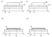
図1は本発明に係る半導体装置の主要な構成を説明するための上面図および断面図である。図1(A)は、特に薄膜トランジスタの要部の上面図を示している。図1(B)は、図1(A)のA1とB1とを結ぶ破線における断面図を示し、図1(C)は、図1(A)のA2とB2とを結ぶ破線における断面図を示している。 1A and 1B are a top view and a cross-sectional view for explaining a main configuration of a semiconductor device according to the present invention. FIG. 1A particularly shows a top view of the main part of the thin film transistor. 1B is a cross-sectional view taken along a broken line connecting A 1 and B 1 in FIG. 1A, and FIG. 1C is a broken line connecting A 2 and B 2 in FIG. FIG.
本実施の形態に示す半導体装置は、基板30上に絶縁層31を介して島状に設けられた半導体層32と、当該半導体層32の上方にゲート絶縁層33を介して設けられたゲート電極として機能する導電層34と、を含む薄膜トランジスタ205と、ゲート絶縁層33および導電層34を覆って設けられた絶縁層203と、絶縁層203上に設けられたソース電極またはドレイン電極として機能する導電層204と、を有している(図1(A)〜(C))。なお、半導体層32は、チャネル形成領域32aと、ソース領域またはドレイン領域として機能する不純物領域32b、32cと、に加えて、半導体層32の端部、ここでは導電層34の下方のチャネル形成領域32aに接した部分に形成された絶縁層36と、を有している。なお、チャネル形成領域32a中に、不純物領域32b、32cに添加した不純物とは逆の導電型の不純物が添加されていてもよい。
The semiconductor device described in this embodiment includes a
ここで、絶縁層36は、半導体層32を酸化することにより形成された酸化膜である。なお、半導体層の端部に形成された絶縁層36は、半導体層32の端部とゲート電極として機能する導電層34が短絡、あるいは半導体層32の端部近傍の電界強度が強くなることで、リーク電流が流れるのを抑制するために設ける。したがって、絶縁層36は、少なくとも半導体層32のチャネル形成領域32aの側面(露出している部分)に形成されていればよい。ただし、それ以外の部分に形成されていてももちろん構わない。
Here, the insulating
本実施の形態において、基板30上に形成された絶縁層31上に半導体層を形成し、半導体層上に選択的にレジストを形成し、レジストをマスクとして半導体層をエッチングすることにより島状の半導体層32を形成できる。そして、レジストを除去する前に半導体層32の端部に対してウェット酸化することにより、半導体層32の端部に絶縁層36を形成できる。そして、レジストを除去して半導体層32および絶縁層36を覆ってゲート絶縁層33を形成し、ゲート絶縁層33上にゲート電極として機能する導電層34を形成する。
In this embodiment mode, a semiconductor layer is formed over the insulating
ここで、ウェット酸化を用いて半導体層32の端部に絶縁層36を形成する方法について説明する。例えば、5ppm以上、望ましくは20ppm以上、より望ましくは100ppm以上のオゾン(O3)を含む水溶液(代表的にはオゾン水)で半導体層32の表面を酸化処理することにより、半導体層32の露出している部分に酸化膜からなる絶縁層36を形成できる。なお、オゾンを含む水溶液にかえて、過酸化水素(H2O2)を含む水溶液、硫酸(H2SO4)を含む水溶液、ヨウ素酸(HIO3)を含む水溶液、または硝酸(HNO3)を含む水溶液等を用いることもできる。また、それぞれの水溶液は、酢酸やしゅう酸等の有機酸を含んでいてもよい。
Here, a method for forming the insulating
なお、本明細書において、上記のように水溶液を用いて半導体層32の露出した部分に酸化膜を形成する処理をウェット酸化という。
Note that in this specification, the process of forming an oxide film on the exposed portion of the
本実施の形態に示す半導体装置は、ゲート電極下の半導体層32のチャネル形成領域32aの端部(側面)に絶縁層36を有するため、ゲート絶縁層33の半導体層32表面への被覆不良が半導体装置に及ぼす影響を低減できる。つまり、半導体層32のチャネル形成領域32aの側面はゲート電極として機能する導電層34と接しないため、ゲートリーク不良を低減し、ゲート電極の耐圧を向上させることが可能となる。
Since the semiconductor device described in this embodiment has the insulating
また、本実施の形態において、半導体層32の端部の露出している部分から酸化を進めることができるため、半導体層32の端部に選択的に厚く酸化膜を形成できる。よって、半導体層32の端部付近における電界集中を緩和でき、ゲートリーク不良を低減し、ゲート電極の耐圧を向上させることが可能となる。
In the present embodiment, since the oxidation can proceed from the exposed portion of the end portion of the
また、半導体層32の端部に形成される絶縁層36より誘電率の大きな材料でゲート絶縁層33を形成することにより、ゲート絶縁層33と半導体層32の端部に形成される絶縁層36とを同程度の膜厚で形成した場合でも、ゲート絶縁層33の実効膜厚に比べて、半導体層32の端部に形成される絶縁層の実効膜厚を厚くすることができる。よって、半導体層32の端部における電界集中を緩和することができる。したがって、ゲートリーク不良を低減し、ゲート電極の耐圧を向上させることが可能となる。
Further, by forming the
半導体層32の端部に形成される絶縁層36より誘電率の大きな材料で形成されるゲート絶縁層33として、気相成長法やスパッタリング法を用いて形成された酸化シリコン膜、窒化シリコン膜、酸化窒化シリコン(SiOxNy)(x>y>0)膜、窒化酸化シリコン(SiNxOy)(x>y>0)膜、Hf系酸化膜等を単層または積層した膜等を用いることができる。
As the
なお、本実施の形態において、半導体層32を形成した後に、ウェット酸化して酸素を含む雰囲気下または窒素を含む雰囲気下で半導体層32表面をプラズマ処理することにより、半導体層32表面に形成された酸化シリコン膜、窒化シリコン膜、酸化窒化シリコン(SiOxNy)(x>y>0)膜または窒化酸化シリコン(SiNxOy)(x>y>0)膜等をゲート絶縁層33として用いることもできる。
Note that in this embodiment, after the
なお、薄膜トランジスタの形状は図1に示すものに限られるものではなく、例えば、ゲート電極として機能する導電層34の側壁に接して、絶縁物からなるサイドウォール701を形成してもよい。また、ソース領域またはドレイン領域として機能する不純物領域32b、32cと、チャネル形成領域32aとの間に、不純物領域32b、32cより低濃度に不純物が添加された低濃度不純物領域(LDD領域)32d、32eが形成されていてもよい(図11(A))。また、薄膜トランジスタの構造として、上述した構造に限られず、チャネル形成領域が2つ形成されるダブルゲート構造または3つ形成されるトリプルゲート構造等のマルチゲート構造を用いることができる。また、ゲート電極を積層構造で設けてもよい。例えば、ゲート電極を、第1の導電層34aと、第1の導電層34a上に形成される第2の導電層34bとの2層構造とし、第1の導電層34aをテーパー状で形成し、第1の導電層34aにのみ重なるように低濃度不純物領域32d、32eを設ける構造(図11(B))としてもよい。また、ゲート電極を、第1の導電層34aと、第1の導電層34a上に形成される第2の導電層34bで設け、第2の導電層34bの側壁に接し、かつ第1の導電層34aの上方に形成されるようにサイドウォール701を設ける構造(図11(C))としてもよい。また、ソース領域またはドレイン領域として機能する不純物領域32b、32cを、Ni、Co、W等のシリサイドで形成することも可能である。
Note that the shape of the thin film transistor is not limited to that illustrated in FIG. 1. For example, a
(実施の形態2)
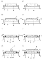
本実施の形態では、図1で示した半導体装置の作製方法の一例に関して図面を参照して説明する。なお、本実施の形態では、図1(A)のA1とB1とを結ぶ破線での断面における作製工程を図2(A)〜(D)を用いて、図1(A)のA2とB2とを結ぶ破線での断面における作製工程を図2(E)〜(H)を用いて説明する。
(Embodiment 2)
In this embodiment, an example of a method for manufacturing the semiconductor device illustrated in FIG. 1 will be described with reference to drawings. Note that in this embodiment, a manufacturing process in a cross-sectional view taken along a broken line connecting A 1 and B 1 in FIG. 1A is described with reference to FIGS. A manufacturing process in a cross section taken along a broken line connecting 2 and B 2 will be described with reference to FIGS.
まず、基板30上に絶縁層31を形成する(図2(A)、(E))。
First, the insulating
基板30は、ガラス基板、石英基板、金属基板(例えばステンレス基板など)、セラミック基板、Si基板等の半導体基板などを用いることができる。また、他にもプラスチック基板として、ポリエチレンテレフタレート(PET)、ポリエチレンナフタレート(PEN)、ポリエーテルサルフォン(PES)、アクリルなどの基板を選択することもできる。
As the
絶縁層31は、基板30からアルカリ金属などの不純物が拡散して、上に形成される素子の汚染を防ぐものであり、ブロッキング層として適宜設ければよい。例えば、CVD法やスパッタリング法等を用いて、酸化シリコン、窒化シリコン、酸化窒化シリコン(SiOxNy)(x>y>0)、窒化酸化シリコン(SiNxOy)(x>y>0)等の絶縁材料を用いて形成できる。例えば、絶縁層31を2層構造とする場合は、第1層目の絶縁層として窒化酸化シリコン膜を形成し、第2層目の絶縁層として酸化窒化シリコン膜を形成するとよい。また、第1層目の絶縁層として窒化シリコン膜を形成し、第2層目の絶縁層として酸化シリコン膜を形成してもよい。
The insulating
続いて、絶縁層31上に半導体層201を形成する。半導体層201は、非晶質半導体膜または結晶質半導体膜で形成できる。結晶性半導体膜としては、絶縁層31上に形成した非晶質半導体膜を熱処理やレーザ光の照射によって結晶化させたものなどを用いることができる。なお、半導体材料としては、シリコンが好ましく、その他にシリコンゲルマニウム等を用いることもできる。
Subsequently, the
半導体層201は、10〜200nm、好ましくは10〜50nm程度、さらに好ましくは10〜30nm程度の膜厚で形成するとよい。なお、50nm以下の半導体層201を形成する場合、50nm以上の膜厚で半導体層を形成した後で、半導体層の表面をドライエッチング処理することにより10〜50nm程度の膜厚の半導体層201を形成してもよい。このときのエッチングの際のエッチングガスとしては、Cl2、BCl3、SiCl4等の塩素系のガス、CF4、NF3、SF6、CHF3等のフッ素系のガス、またはフッ素系ガスにHeやAr等の不活性ガス、O2ガス、H2ガス、を適宜加えた混合ガス等を用いることができる。なお、ドライエッチングの前に、半導体層表面を希フッ酸処理して半導体層表面に形成される自然酸化膜を除去し、その後半導体層表面をオゾン水などで処理して半導体層表面に酸化膜を形成しておいてもよい。
The
半導体層201を50nm以下程度の薄膜で形成することにより、半導体層表面に形成されるゲート絶縁層の被覆不良を低減することができる。また、半導体層201を薄膜で形成することにより、TFTをより小型化することができる。また、TFTのしきい値電圧を小さくするためにチャネル形成領域への不純物元素のドープ量を増加させた場合でも、半導体層201を薄膜で形成することにより完全空乏型のTFTを作製しやすくなるため、良好なS値でしきい値電圧の小さなTFTを作製することができる。
By forming the
また、非結晶半導体膜をレーザ光の照射によって結晶化もしくは再結晶化した膜を半導体層201として用いる場合、レーザ光の光源としてLD励起の連続発振(CW)レーザ(YVO4、第2高調波(波長532nm))を用いることができる。特に第2高調波に限定する必要はないが、第2高調波はエネルギー効率の点で、さらに高次の高調波より優れている。CWレーザを半導体層に照射すると、連続的に半導体層にエネルギーが与えられるため、一旦半導体層を溶融状態にすると、溶融状態を継続させることができる。さらに、CWレーザを走査することによって半導体層の固液界面を移動させ、この移動の方向に沿って一方向に長い結晶粒を形成することができる。また、固体レーザを用いるのは、気体レーザ等と比較して、出力の安定性が高く、安定した処理が見込まれるためである。なお、CWレーザに限らず、繰り返し周波数が10MHz以上のパルスレーザを用いることも可能である。繰り返し周波数が高いパルスレーザを用いると、半導体層が溶融してから固化するまでの時間よりもレーザのパルス間隔が短ければ、常に半導体層を溶融状態にとどめることができ、固液界面の移動により一方向に長い結晶粒で構成される半導体層を形成できる。また、その他のCWレーザおよび繰り返し周波数が10MHz以上のパルスレーザを使用することもできる。例えば、気体レーザとしては、Arレーザ、Krレーザ、CO2レーザなどがある。固体レーザとして、YAGレーザ、YLFレーザ、YAlO3レーザ、GdVO4レーザ、KGWレーザ、KYWレーザ、アレキサンドライトレーザ、Ti:サファイアレーザ、Y2O3レーザ、YVO4レーザなどがある。また、YAGレーザ、Y2O3レーザ、GdVO4レーザ、YVO4レーザなどのセラミックスレーザがある。金属蒸気レーザとしてはヘリウムカドミウムレーザなどが挙げられる。また、レーザ発振器において、レーザ光をTEM00(シングル横モード)で発振して射出すると、被照射面において得られる線状のビームスポットのエネルギー均一性を上げることができるので好ましい。その他にも、パルス発振のエキシマレーザを用いてもよい。
In the case where a film obtained by crystallizing or recrystallizing an amorphous semiconductor film by laser light irradiation is used as the
次に、半導体層201上にレジスト202を選択的に形成する(図2(A)、(E))。なお、半導体層上に酸化膜を形成してから、レジストを形成してもよい。そして、レジスト202をマスクとして半導体層201をドライエッチングして、島状の半導体層32を形成する(図2(B)、(F))。なお、レジスト202は、エッチングの際のマスクとして用いるものであり、ポジ型のフォトレジストやネガ型のフォトレジスト等を適宜選択して用いることができる。
Next, a resist 202 is selectively formed over the semiconductor layer 201 (FIGS. 2A and 2E). Note that a resist may be formed after an oxide film is formed over the semiconductor layer. Then, the
ドライエッチングのときのエッチングガスとしては、CF4、NF3、SF6、CHF3等のフッ素系のガス、または該フッ素系ガスにHeやAr等の不活性ガス、O2ガス、H2ガス、を適宜加えた混合ガス等を用いることができる。好ましくは、CF4とO2との混合ガス、SF6とO2との混合ガス、CHF3とHeとの混合ガス、またはCF4とH2との混合ガスを用いるとよい。また、エッチングはドライエッチングに限られず、ウェットエッチングで行ってもよい。その場合、半導体層201に対し、TMAH(tetramethylammonium hydroxide、テトラメチルアンモニウムヒドロキシド)に代表される有機アルカリ系水溶液を用いてウェットエッチングすることにより、島状の半導体層32を形成できる。なお、エッチング液としてTMAH等を用いた場合、半導体層201のみが選択的にエッチングされるため、下地の絶縁層31にダメージを与えずにエッチングできる。このように、絶縁表面に形成された半導体層を島状に分離形成することで、同一基板上に複数の薄膜トランジスタと周辺回路を形成した場合に、それぞれの素子を分離できる。すなわち、10V〜20V程度の電圧で書き込みや消去を行う必要のあるメモリ素子アレイと、3V〜7V程度の電圧で動作してデータの入出力や命令の制御を主として行う周辺回路を同一基板上に形成した場合でも、各素子に印加する電圧の違いによる相互の干渉を防ぐことができる。
As an etching gas during dry etching, a fluorine-based gas such as CF 4 , NF 3 , SF 6 , or CHF 3 , or an inert gas such as He or Ar, an O 2 gas, or an H 2 gas is used as the fluorine-based gas. A mixed gas or the like appropriately added can be used. Preferably, a mixed gas of CF 4 and O 2 , a mixed gas of SF 6 and O 2 , a mixed gas of CHF 3 and He, or a mixed gas of CF 4 and H 2 may be used. Etching is not limited to dry etching, and may be performed by wet etching. In that case, the island-shaped
また、島状の半導体層32の端部の断面形状は、必ずしもテーパー状になっている必要はない。半導体層32の端部付近に形成される膜の被覆不良の低減を考慮すると、よりθの角度が小さいほうが好ましいが、θが45°〜95°程度のテーパー状や垂直形状にエッチングしてもよい。
In addition, the cross-sectional shape of the end portion of the island-shaped
続いて、半導体層32の端部に絶縁層36を形成する(図2(B)、(F))。ここで、絶縁層36は、実施の形態1と同様に、半導体層32の端部をウェット酸化することにより形成された酸化膜である。
Subsequently, an insulating
続いて、半導体層32を覆うようにゲート絶縁層33を形成する。ゲート絶縁層33は、酸化シリコン、窒化シリコン、酸化窒化シリコン(SiOxNy)(x>y>0)、窒化酸化シリコン(SiNxOy)(x>y>0)等を用いて形成できる。このような絶縁層は、気相成長法やスパッタリング法で形成できる。また、酸素を含む雰囲気下または窒素を含む雰囲気下で半導体層32表面をプラズマ処理することにより、半導体層32表面に形成された酸化シリコン膜、窒化シリコン膜、酸化窒化シリコン(SiOxNy)(x>y>0)膜、または窒化酸化シリコン(SiNxOy)(x>y>0)膜等をゲート絶縁層33として用いることもできる。
Subsequently, a
次に、ゲート絶縁層33上にゲート電極として機能する導電層34を形成する(図2(C)、(G))。ここでは、導電層34は単層で形成した例を示しているが、もちろん、導電性材料を2層または3層以上の積層で設けた構造としてもよい。なお、ここでは図示しないが、導電層34は、ゲート絶縁層33上を覆って形成された導電層を選択的にエッチングすることにより形成できる。
Next, a
また、導電層34は、タンタル(Ta)、タングステン(W)、チタン(Ti)、モリブデン(Mo)、アルミニウム(Al)、銅(Cu)、クロム(Cr)、ニオブ(Nb)等から選択された元素、またはこれらの元素を主成分とする合金材料、もしくは化合物材料で形成できる。また、リン等の不純物元素をドーピングした多結晶珪素に代表される半導体材料により形成することもできる。例えば、導電層34を第1の導電層と第2の導電層との積層構造とする場合、第1の導電層として窒化タンタルを用い、第2の導電層としてタングステンを用いて形成するとよい。なお、この組み合わせに限られず、導電層34を積層して形成する場合には、上記材料を自由に組み合わせて設けることができる。
The
続いて、導電層34をマスクとして、半導体層32に不純物元素121を導入することによって、半導体層32に不純物領域32b、32cおよび不純物元素121が導入されないチャネル形成領域32aを形成する(図2(C)、(G))。なお、ここでは、島状の半導体層32を横断するように導電層34を形成した後に、不純物元素を導入するため、導電層34に覆われていない半導体層32の領域に不純物領域32b、32cが形成され、導電層34に覆われた半導体層32の領域に不純物元素121が導入されないチャネル形成領域32aが形成される。
Subsequently, by using the
ここで、不純物元素121としては、n型を付与する不純物元素またはp型を付与する不純物元素を用いることができる。n型を示す不純物元素としては、リン(P)やヒ素(As)等を用いることができる。p型を示す不純物元素としては、ボロン(B)やアルミニウム(Al)やガリウム(Ga)等を用いることができる。例えば、不純物元素121として、リン(P)を1×10¹⁸〜1×10²¹/cm3の濃度で含むように半導体層32に導入し、n型を示す不純物領域32b、32cを形成すればよい。なお、チャネル形成領域32aと不純物領域32b、32cとの間に、不純物領域32b、32cより低濃度に不純物が添加された低濃度不純物領域(LDD領域)を形成してもよい。低濃度不純物領域を設けることにより、LDD領域側のドレイン端部の電界を緩和して、書き込みおよび消去の繰り返しによる劣化を抑制できる。
Here, as the
また、チャネル形成領域32a中に、不純物領域32b、32cに添加した不純物とは逆の導電型を有する不純物元素(例えばn型TFTに対してはボロン)を添加してもよい。チャネル形成領域32a中に逆導電型の不純物を添加することにより、TFTのしきい値電圧を制御できる。なお、この不純物元素はゲート電極を介してドープすることよって添加してもよいし、ゲート電極形成前に予め添加しておいてもよい。
Further, an impurity element having a conductivity type opposite to that of the impurity added to the
次に、導電層34、ゲート絶縁層33、絶縁層31等を覆うように絶縁層203を形成する(図2(D)、(H))。その後、ゲート絶縁層33および絶縁層203にコンタクトホールを形成し、絶縁層203上にソース電極またはドレイン電極として機能する導電層204を選択的に形成する(図2(D)、(H))。ここで、導電層204は、半導体層32のソース領域またはドレイン領域として機能する不純物領域32b、32cと電気的に接続されるように設ける。
Next, the insulating
絶縁層203は、CVD法やスパッタリング法等で形成した、酸化シリコン、酸化窒化シリコン(SiOxNy)(x>y>0)、窒化酸化シリコン(SiNxOy)(x>y>0)などを用いることができる。また、ポリイミド、ポリアミド、ポリビニルフェノール、ベンゾシクロブテン、アクリル、エポキシ等の有機材料、またはシロキサン樹脂等のシロキサン材料、オキサゾール樹脂等からなる単層または積層構造で設けることができる。なお、シロキサン材料とは、Si−O−Si結合を含む材料に相当する。シロキサンは、シリコン(Si)と酸素(O)との結合で骨格構造が構成される。置換基として、少なくとも水素を含む有機基(例えばアルキル基、アリール基)が用いられる。置換基として、フルオロ基を用いることもできる。オキサゾール樹脂は、例えば、感光性ポリベンゾオキサゾール等である。感光性ポリベンゾオキサゾールは、誘電率が低く(常温1MHzで誘電率2.9)、耐熱性が高く(示差熱熱重量同時測定(TG/DTA:Thermogravimetry−Differential Thermal Analysis)で昇温5℃/minで熱分解温度550℃)、吸水率が低い(常温24時間で0.3%)材料である。オキサゾール樹脂は、ポリイミド等の比誘電率(3.2〜3.4程度)と比較すると、比誘電率が低いため(2.9程度)、寄生容量の発生を抑制し、高速に動作できる。ここでは、絶縁層203として、CVD法で形成した酸化シリコン、酸化窒化シリコン(SiOxNy)(x>y>0)または窒化酸化シリコン(SiNxOy)(x>y>0)を単層または積層して形成する。また、さらに、ポリイミド、ポリアミド、ポリビニルフェノール、ベンゾシクロブテン、アクリル、エポキシ等の有機材料、シロキサン樹脂等のシロキサン材料、またはオキサゾール樹脂を積層して形成してもよい。
As the insulating
また、導電層204は、アルミニウム、タングステン、チタン、タンタル、モリブデン、ニッケル、ネオジムから選ばれた1種の元素、または当該元素を複数含む合金からなる単層構造または積層構造を用いることができる。例えば、当該元素を複数含む合金からなる導電層204として、チタンを含有したアルミニウム合金、ネオジムを含有したアルミニウム合金などで形成できる。また、積層構造で導電層204を設ける場合、例えば、アルミニウム層もしくは前記したようなアルミニウム合金層を、チタン層で挟んで積層させた構造としてもよい。
The
以上の工程により、薄膜トランジスタ205を含む半導体装置を作製できる。
Through the above steps, a semiconductor device including the
本実施の形態に示す半導体装置の作製工程を用いることにより、ゲート電極下の半導体層32のチャネル形成領域32aの端部(側面)に、絶縁層36を有する半導体装置を作製することができる。したがって、ゲート絶縁層33の半導体層32表面への被覆不良が、半導体装置に及ぼす影響を低減できる。つまり、本実施の形態の方法を用いて作製された半導体装置は、半導体層32のチャネル形成領域32aの側面がゲート電極と接することがなくなるため、ゲートリーク不良を低減し、ゲート電極の耐圧を向上させることが可能となる。
By using the manufacturing process of the semiconductor device described in this embodiment, a semiconductor device including the insulating
また、半導体層32のチャネル形成領域32aの端部に、選択的に厚く絶縁層を設けることができるため、半導体層32のチャネル形成領域32aの端部における電界集中を緩和することができる。したがって、ゲートリーク不良を低減し、ゲート電極の耐圧を向上させることが可能となる。
In addition, since an insulating layer can be selectively provided thick at the end of the
本実施の形態において、酸素を含む雰囲気下または窒素を含む雰囲気下で、半導体層32表面をプラズマ処理してゲート絶縁層33を形成する際、電子密度が1×1011cm−3以上であり、電子温度が1.5eV以下のプラズマを用いるとよい。より詳しくは、電子密度が1×1011cm−3以上1×1013cm−3以下で、電子温度が0.5eV以上1.5eV以下のプラズマを用いるとよい。上記プラズマは、プラズマの電子密度が高密度であり、基板30上に形成された被処理物(ここでは、半導体層32)付近での電子温度が低いため、被処理物に対するプラズマによる損傷を防止できる。また、プラズマの電子密度が1×1011cm−3以上と高密度であるため、プラズマ処理を用いて形成される酸化膜または窒化膜は、CVD法やスパッタ法等により形成された膜と比較して、膜厚等が均一性に優れ、かつ緻密な膜を形成できる。また、プラズマの電子温度が1.5eV以下と低いため、従来のプラズマ処理や熱酸化法と比較して低い温度で酸化または窒化処理できる。例えば、ガラス基板の歪点よりも100度以上低い温度でプラズマ処理を行っても十分に酸化できる。また、プラズマを形成するための周波数としては、マイクロ波(2.45GHz)等の高周波を用いることができる。
In this embodiment, when the
なお、酸素を含む雰囲気下として、例えば、酸素(O2)と希ガス(He、Ne、Ar、Kr、Xeの少なくとも1つを含む)との混合ガス雰囲気下、酸素と水素(H2)と希ガスとの混合ガス雰囲気下、一酸化二窒素と希ガスとの混合ガス雰囲気下、または一酸化二窒素と水素と希ガスとの混合ガス雰囲気下でプラズマ処理できる。例えば、酸素(O2)と水素(H2)とアルゴン(Ar)との混合ガスを用いることができる。その場合、酸素を0.1〜100sccm、水素を0.1〜100sccm、アルゴンを100〜5000sccm含んだ混合ガスを用いることができる。なお、酸素:水素:アルゴン=1:1:100の比率で混合ガスを導入することが好ましい。例えば、酸素を5sccm、水素を5sccm、アルゴンを500sccmとして導入すればよい。 Note that as an atmosphere containing oxygen, for example, oxygen and hydrogen (H 2 ) in a mixed gas atmosphere of oxygen (O 2 ) and a rare gas (including at least one of He, Ne, Ar, Kr, and Xe). And a rare gas mixed gas atmosphere, a mixed gas atmosphere of dinitrogen monoxide and a rare gas, or a mixed gas atmosphere of dinitrogen monoxide, hydrogen, and a rare gas. For example, a mixed gas of oxygen (O 2 ), hydrogen (H 2 ), and argon (Ar) can be used. In that case, a mixed gas containing 0.1 to 100 sccm of oxygen, 0.1 to 100 sccm of hydrogen, and 100 to 5000 sccm of argon can be used. Note that the mixed gas is preferably introduced at a ratio of oxygen: hydrogen: argon = 1: 1: 100. For example, oxygen may be introduced at 5 sccm, hydrogen at 5 sccm, and argon at 500 sccm.
また、窒素を含む雰囲気下として例えば、窒素(N2)と希ガス(He、Ne、Ar、Kr、Xeの少なくとも1つを含む)との混合ガス雰囲気下、窒素と水素と希ガスとの混合ガス雰囲気下、またはアンモニア(NH3)と希ガスとの混合ガス雰囲気下でプラズマ処理できる。 Further, as an atmosphere including nitrogen, for example, in a mixed gas atmosphere of nitrogen (N 2 ) and a rare gas (including at least one of He, Ne, Ar, Kr, and Xe), nitrogen, hydrogen, and a rare gas Plasma treatment can be performed in a mixed gas atmosphere or a mixed gas atmosphere of ammonia (NH 3 ) and a rare gas.
ここで、プラズマ処理するための装置の構成例について図17を用いて説明する。 Here, a configuration example of an apparatus for plasma processing will be described with reference to FIG.
図17に示すプラズマ処理装置は、基板210を配置するための支持台280、ガスを導入するためのガス供給部276、ガスを排気するために真空ポンプに接続する排気口278、アンテナ272、誘電体板274およびプラズマ発生用のマイクロ波を供給するマイクロ波供給部284を有している。また、支持台280に温度制御部282を設けることによって、基板210の温度を制御することも可能である。
The plasma processing apparatus shown in FIG. 17 includes a
以下に、プラズマ処理方法の一例について説明する。 Hereinafter, an example of the plasma processing method will be described.
酸化処理もしくは窒化処理を行うには、以下のようにすればよい。まず、処理室内を真空にし、ガス供給部276から酸素または窒素を含むプラズマ処理用ガスを導入する。基板210は、室温もしくは温度制御部282により100〜550℃に加熱する。なお、基板210と誘電体板274との間隔は、20mm〜80mm(好ましくは20mm〜60mm)程度である。次に、マイクロ波供給部284からアンテナ272に、マイクロ波を供給する。そしてマイクロ波を、アンテナ272から誘電体板274を通して処理室内に導入することによって、プラズマ286を生成する。マイクロ波の導入によりプラズマの励起を行うと、低電子温度(3eV以下、好ましくは1.5eV以下)で高電子密度(1×1011cm−3以上)のプラズマを生成できる。この高密度プラズマで生成された酸素ラジカル(OHラジカルを含む場合もある)および/または窒素ラジカル(NHラジカルを含む場合もある)によって、半導体基板の表面を酸化または窒化することができる。プラズマ処理用ガスにアルゴンなどの希ガスを混合させると、希ガスの励起種により酸素ラジカルや窒素ラジカルを効率良く生成できる。このプラズマ処理方法では、プラズマで励起した活性なラジカルを有効に使うことにより、500℃以下の低温で固相反応による酸化処理または窒化処理ができる。
In order to perform oxidation treatment or nitridation treatment, the following may be performed. First, the processing chamber is evacuated and a plasma processing gas containing oxygen or nitrogen is introduced from the
上記のようなプラズマ処理による固相酸化処理または固相窒化処理を用いることで、耐熱温度が700℃以下のガラス基板を用いても、950℃〜1050℃で形成される熱酸化膜と同等な絶縁層を得ることができる。すなわち、半導体素子、特に薄膜トランジスタや不揮発性記憶素子の絶縁層として信頼性の高い絶縁層を形成できる。 By using the solid-phase oxidation treatment or solid-phase nitridation treatment by plasma treatment as described above, even if a glass substrate having a heat resistant temperature of 700 ° C. or lower is used, it is equivalent to a thermal oxide film formed at 950 ° C. to 1050 ° C. An insulating layer can be obtained. That is, a highly reliable insulating layer can be formed as an insulating layer of a semiconductor element, particularly a thin film transistor or a nonvolatile memory element.
例えば、図17に示すプラズマ処理装置を用いてゲート絶縁層33を形成する場合、酸化雰囲気下のプラズマ処理により、例えば、シリコンからなる半導体層32の表面を酸化して3〜6nmの厚さの酸化珪素層を形成し、その後、該酸化珪素層の表面を窒素雰囲気下でプラズマ処理した窒素プラズマ処理層を形成することが好ましい。具体的には、まず、酸素雰囲気下でのプラズマ処理により、半導体層32上に3〜6nmの厚さで酸化珪素層を形成する。その後、続けて窒素雰囲気下でプラズマ処理を行うことにより、酸化珪素層の表面または表面近傍に窒素濃度の高い窒素プラズマ処理層を設ける。なお、表面近傍とは、酸化珪素層の表面から概略0.5〜1.5nmの深さをいう。例えば、窒素雰囲気下でプラズマ処理を行うことによって、酸化珪素層の表面から概略1nmの深さに、窒素を20〜50原子%の割合で含有した構造となる。酸化珪素層表面を窒化することにより、さらに層を緻密化することができ、絶縁耐圧が高い絶縁層を形成できる。
For example, when the
なお、本実施の形態で示すプラズマ処理装置は、半導体基板、絶縁層、導電層に対する酸化処理、窒化処理、酸窒化処理、水素化処理、表面改質処理等を行うことができる。これらの処理を行う際は、その目的に応じてガス供給部276から供給するガスを適宜選択すればよい。
Note that the plasma treatment apparatus described in this embodiment can perform oxidation treatment, nitridation treatment, oxynitridation treatment, hydrogenation treatment, surface modification treatment, or the like on a semiconductor substrate, an insulating layer, and a conductive layer. When performing these processes, a gas supplied from the
(実施の形態3)
本実施の形態では、図1に示す半導体装置の作製方法について、実施の形態2とは異なる方法について説明する。本実施の形態では図1(A)のA1とB1とを結ぶ破線での断面における作製工程を図3(A)〜(B)を用いて、図1(A)のA2とB2とを結ぶ破線での断面における作製工程を図3(C)〜(D)を用いて説明する。
(Embodiment 3)
In this embodiment, a method for manufacturing the semiconductor device illustrated in FIGS. 1A to 1C is different from that in
まず、実施の形態2と同様に、基板30上に絶縁層31を形成し、絶縁層31上に半導体層201を形成し、半導体層201上にレジスト202を形成する(図3(A)、(C))。
First, as in
続いて、レジスト202をマスクとして半導体層201をエッチングすることにより、島状の半導体層32を形成する(図3(B)、(D))。
Subsequently, the
続いて、レジスト202を除去した後、半導体層32表面をウェット酸化することにより、半導体層32の端部および表面に絶縁層36を形成する。
Subsequently, after the resist 202 is removed, the surface of the
以降の工程は、実施の形態2と同様に行うことにより、図1に示す半導体装置を作製できる。
The subsequent steps are performed in the same manner as in
なお、半導体層32の表面をウェット酸化して絶縁層36を形成する前に、必要に応じて半導体層32表面を希フッ酸等で洗浄する工程を行ってもよい。半導体層32の表面は、大気中の酸素に半導体層32が触れて酸化され自然酸化膜が形成されていたり、ゴミが付着していたりするため、洗浄することが好ましい。しかしながら、半導体層32を洗浄する際、図4(A)に示すように、半導体層32の下地膜として形成されている絶縁層31も部分的に除去され、窪み37が形成されることがある。窪み37が形成された場合に、半導体層32上にゲート絶縁層を形成すると、半導体層32および窪み37の段差を覆いきれず、ゲート絶縁層が部分的に切断されてしまうことがある。すると、半導体層32とゲート電極として機能する導電層とが接して、半導体層32およびゲート電極として機能する導電層の間でリーク電流が生じてしまう可能性がある。
Note that before the surface of the
しかしながら、本実施の形態で示すように、半導体層表面をウェット酸化して、半導体層32の端部および表面に絶縁層36を形成することにより、図4(B)に示すように、窪み37部分でゲート絶縁層33の被覆不良が生じても、半導体層32のチャネル形成領域とゲート電極として機能する導電層とが接することがなくなる。
However, as shown in this embodiment, the surface of the semiconductor layer is wet-oxidized to form the insulating
また、半導体層32表面を希フッ酸処理した後、ゲート絶縁層33を形成してから、ウェット酸化してもよい。図5に、半導体層32表面を希フッ酸処理した後の素子の断面構造を示す。図5(A)、(E)は、希フッ酸処理によって絶縁層31が部分的に除去されている様子を示す。
Further, after the surface of the
次に、半導体層32上に、ゲート絶縁層33を形成する(図5(B)、(F))。なお、ゲート絶縁層33は上記実施の形態のゲート絶縁層33と同様に作製することができる。ここで、絶縁層31が部分的に除去されているため、ゲート絶縁層33は半導体層32の下側には形成されない可能性がある。
Next, the
次に、ゲート絶縁層33の表面をウェット酸化する。ここで、半導体層32表面のゲート絶縁層33で覆われていない部分がウェット酸化されて、ゲート絶縁層33で覆われていない半導体層32表面に絶縁層36を形成できる(図5(C)、(G))。
Next, the surface of the
次に、ゲート絶縁層33上に、ゲート電極として機能する導電層34を形成する(図5(D)、(H))。なお、導電層34は、上記実施の形態で示した導電層34と同様に形成できる。
Next, a
半導体層32表面を希フッ酸処理した後、ゲート絶縁層33を形成してからさらにウェット酸化を行うことによって、ゲート絶縁層33で覆われない半導体層32表面にも絶縁層36を形成できる。したがって、半導体層32の表面は、ゲート電極として機能する導電層34と接しない構成とできる。
After the surface of the
本実施の形態に示す半導体装置の作製工程を用いることにより、ゲート電極下の半導体層32のチャネル形成領域32aの端部(側面)に、絶縁層36を有する半導体装置を作製できる。したがって、ゲート絶縁層33の半導体層32表面への被覆不良が、半導体装置に及ぼす影響を低減できる。つまり、本実施の形態の方法を用いて作製された半導体装置において、半導体層32のチャネル形成領域32aの側面は、ゲート電極と接することがないため、ゲートリーク不良を低減し、ゲート電極の耐圧を向上させることが可能となる。
By using the manufacturing process of the semiconductor device described in this embodiment, a semiconductor device including the insulating
また、半導体層32のチャネル形成領域32aの端部に選択的に厚く絶縁層を設けることができるため、半導体層32のチャネル形成領域32aの端部における電界集中を緩和できる。したがって、ゲートリーク不良を低減し、ゲート電極の耐圧を向上させることが可能となる。
Further, since an insulating layer can be selectively provided thick at the end of the
(実施の形態4)
本実施の形態では、図1に示す半導体装置の作製方法について、実施の形態2または実施の形態3とは異なる方法について説明する。本実施の形態では、図1(A)のA1とB1とを結ぶ破線での断面における作製工程を図6(A)〜(D)を用いて、図1(A)のA2とB2とを結ぶ破線での断面における作製工程を図6(E)〜(H)を用いて説明する。
(Embodiment 4)
In this embodiment, a method for manufacturing the semiconductor device illustrated in FIGS. 1A to 1C is different from that in
まず、実施の形態2と同様に、基板30上に絶縁層31を形成し、絶縁層31上に半導体層201を形成し、半導体層201上にレジスト202を形成する(図6(A)、(E))。
First, as in
次に、レジスト202をマスクとして半導体層201をエッチングすることにより、島状の半導体層32を形成する(図6(B)、(F))。続いて、レジスト202を除去し、半導体層32表面を希フッ酸で洗浄する(図6(B)、(F))。ここで、半導体層32上に第1の絶縁層33を形成する前に、半導体層32表面を希フッ酸で処理することにより、半導体層32表面に形成される自然酸化膜を除去できる。
Next, the
次に、半導体層32上にレジスト301を形成する(図6(C)、(G))。ここで、レジスト301は、半導体層32より内側の領域に形成する。つまり、レジスト301は、半導体層32の表面を部分的に覆っている。
Next, a resist 301 is formed over the semiconductor layer 32 (FIGS. 6C and 6G). Here, the resist 301 is formed in a region inside the
なお、半導体層32の表面を部分的に覆うレジスト301は、半導体層201表面に形成されたレジスト202を除去せず、レジスト202を部分的にエッチングしてレジスト202の側面を後退させることにより形成してもよい。つまり、まず図6(A)、(E)と同様に基板30上に絶縁層31を形成し、絶縁層31上に半導体層201を形成し、半導体層201上にレジスト202を形成する(図7(A)、(D))。次に、レジスト202をマスクとして半導体層201をエッチングすることにより、島状の半導体層32を形成する(図7(B)、(E)))。続いて、レジスト202をエッチングしてレジスト202の側面を後退させる。これにより、レジスト202の幅が細くなり、半導体層32の表面が部分的に覆われたレジスト301が形成される。
Note that the resist 301 that partially covers the surface of the
次に、レジスト301をマスクとして半導体層32表面をウェット酸化することにより、半導体層32の端部および上面の一部に絶縁層36を形成する(図6(C)、(G))。
Next, the surface of the
次に、レジスト301を除去して、半導体層32上にゲート絶縁層33を形成する。さらに、ゲート絶縁層33上にゲート電極として機能する導電層34を形成する(図6(D)、(H))。なお、ゲート絶縁層33および導電層34はそれぞれ、上記実施の形態で説明したゲート絶縁層33および導電層34と同様に形成できる。
Next, the resist 301 is removed, and the
以降、実施の形態2と同様の工程を行うことにより、図1に示すような半導体装置を作製できる。
Thereafter, by performing the same steps as in
半導体層32の端部および上面の一部に絶縁層36が形成されているため、より電界が集中しやすい半導体層32の角部(図6(D)、(H)の領域501付近)において、導電層34下に形成される絶縁層の膜厚を厚くできる。したがって、より電界集中を防ぐことができる。
Since the insulating
本実施の形態に示す半導体装置の作製工程を用いることにより、ゲート電極下の半導体層のチャネル形成領域32aの端部(側面)に、絶縁層36を有する半導体装置を作製できる。したがって、ゲート絶縁層33の半導体層32表面への被覆不良が、半導体装置に及ぼす影響を低減できる。つまり、本実施の形態の方法を用いて作製された半導体装置は、半導体層32のチャネル形成領域32aの側面が、ゲート電極と接することがなくなるため、ゲートリーク不良を低減し、ゲート電極の耐圧を向上させることが可能となる。
By using the manufacturing process of the semiconductor device described in this embodiment, a semiconductor device including the insulating
(実施の形態5)
本実施の形態では、単結晶シリコン基板上に酸化シリコンでなる酸化膜を形成し、酸化膜上に形成された単結晶半導体薄膜をチャネル形成領域として用いる半導体装置について説明する。本実施の形態では、SIMOXと呼ばれるSOI技術を用いた半導体装置について説明する。
(Embodiment 5)
In this embodiment, a semiconductor device in which an oxide film made of silicon oxide is formed over a single crystal silicon substrate and a single crystal semiconductor thin film formed over the oxide film is used as a channel formation region will be described. In this embodiment, a semiconductor device using an SOI technology called SIMOX will be described.
まず、単結晶シリコン層の形成材料となる単結晶シリコン基板601を用意する(図8(A))。ここではP型の単結晶シリコン基板を用いる場合を説明するが、N型の単結晶シリコン基板であってもよい。もちろん、単結晶シリコンゲルマニウム基板を用いることもできる。
First, a single
続いて、単結晶シリコン基板601に対して酸素イオンを添加し、所定の深さに酸素含有層602を形成する(図8(B))。酸素イオンは、例えば1×10¹⁸atoms/cm2程度のドーズ量で添加すればよい。なお、酸素含有層602が形成される深さ(単結晶シリコン基板601の主表面と酸素含有層602との間の距離)は、後に形成されるTFTの活性層として機能する単結晶シリコン層の膜厚となる。
Subsequently, oxygen ions are added to the single
次に、800〜1200℃の温度で熱処理を行い、酸素含有層602を埋め込み絶縁層603に変化させる。酸素含有層602の深さ方向の幅は、イオン添加時の酸素イオンの分布で決まっている。酸素イオンの濃度が611から612に向かって減少していくため、単結晶シリコン基板601と酸素含有層602との界面は不明確であるが、この熱処理工程により単結晶シリコン基板601と埋め込み絶縁層603との界面は明確なものとなる(図8(B)、(C))。
Next, heat treatment is performed at a temperature of 800 to 1200 ° C. to change the oxygen-containing
この埋め込み絶縁層603の膜厚は10〜500nm(代表的には20〜50nm)とする。本実施の形態では、単結晶シリコン基板601と埋め込み絶縁層603の界面が安定に接合されているため、20〜50nmといった薄い埋め込み絶縁層603を形成することができる。
The buried insulating
こうして埋め込み絶縁層603が形成されると、埋め込み絶縁層603の上には部分的に単結晶シリコン基板の一部が残存し、単結晶シリコン層604が形成される。なお、単結晶シリコン層604の膜厚は10〜200nm(好ましくは10〜50nm、さらに好ましくは10〜30nm)となるように、酸素含有層602が形成される深さを調節すればよい。
When the buried insulating
次に、単結晶シリコン層604上に選択的にレジストを形成して、単結晶シリコン層604を選択的にエッチングすることにより、後に形成されるTFTの活性層となる、島状の単結晶シリコン層605を形成する(図8(D))。なお、本実施の形態では1つの島状の単結晶シリコン層しか記載していないが、同一基板上に複数個が形成されていてもよい。
Next, a resist is selectively formed on the single
以降、実施の形態2または実施の形態3と同様の工程を行うことにより、図9に示すような半導体装置を作製することができる。なお、本実施の形態において、半導体装置として薄膜トランジスタの例を示す。図9(A)は、薄膜トランジスタの要部の上面図を示し、図9(B)は、図9(A)のA1とB1とを結ぶ破線における断面図を示し、図9(C)は、図9(A)のA2とB2とを結ぶ破線における断面図を示している。
Thereafter, by performing the same steps as those in
図9に示す薄膜トランジスタは、単結晶シリコン基板601上に埋め込み絶縁層603を介して設けられた島状の単結晶シリコン層605と、島状の単結晶シリコン層605上に形成されたゲート絶縁層33と、島状の単結晶シリコン層605の上方にゲート絶縁層33を介して設けられたゲート電極として機能する導電層34と、ゲート絶縁層33および導電層34を覆って設けられた絶縁層203と、絶縁層203上に設けられたソース電極またはドレイン電極として機能する導電層204と、を有している。なお、島状の単結晶シリコン層605は、チャネル形成領域605aとソース領域またはドレイン領域として機能する不純物領域605b、605cとに加えて、島状の単結晶シリコン層605の端部、ここでは導電層34の下方のチャネル形成領域605aに接した部分に形成された絶縁層36とを有している。なお、絶縁層36は、島状の単結晶シリコン層605の表面を、酸素を含む雰囲気中でプラズマ処理することにより形成できる。なお、チャネル形成領域605a中に、不純物領域605b、605cに添加した不純物とは逆の導電型の不純物が添加されていてもよい。
9 includes an island-shaped single
本実施の形態によって、ゲート電極下の単結晶シリコン層605のチャネル形成領域605aの端部(側面)に、絶縁層36を有する半導体装置を作製できる。したがって、ゲート絶縁層33の単結晶シリコン層605表面への被覆不良が、半導体装置に及ぼす影響を低減できる。つまり、本実施の形態の方法を用いて作製された半導体装置は、単結晶シリコン層605のチャネル形成領域605aの側面がゲート電極と接しないため、電界集中が生じず、ゲートリーク不良を低減し、ゲート電極の耐圧を向上させることが可能となる。
According to this embodiment mode, a semiconductor device having the insulating
また、単結晶シリコン層605のチャネル形成領域605aの端部に、選択的に厚く絶縁層を設けることができるため、単結晶シリコン層605のチャネル形成領域605aの端部における電界集中を緩和できる。したがって、ゲートリーク不良を低減し、ゲート電極の耐圧を向上させることが可能となる。
Further, since an insulating layer can be selectively provided thick at an end portion of the
(実施の形態6)
本実施の形態では、単結晶シリコン基板上に酸化シリコンでなる酸化膜を形成し、酸化膜上に形成された単結晶半導体薄膜をチャネル形成領域として用いる半導体装置について説明する。本実施の形態では、Smart−Cut法を用いて形成されるSOI基板を用いた半導体装置について説明する。
(Embodiment 6)
In this embodiment, a semiconductor device in which an oxide film made of silicon oxide is formed over a single crystal silicon substrate and a single crystal semiconductor thin film formed over the oxide film is used as a channel formation region will be described. In this embodiment, a semiconductor device using an SOI substrate formed using a Smart-Cut method is described.
まず、単結晶シリコン層の形成材料となる、単結晶シリコン基板801を用意する。ここではP型の単結晶シリコン基板を用いる場合を説明するが、N型の単結晶シリコン基板であってもよい。もちろん、単結晶シリコンゲルマニウム基板を用いることもできる。
First, a single
次いで熱酸化処理を行い、その主表面(素子形成面に相当する)に酸化シリコン膜802を形成する。膜厚は実施者が適宜決定すればよいが、10〜500nm(代表的には20〜50nm)とすればよい。この酸化シリコン膜802は、後にSOI基板の埋め込み絶縁層の一部として機能する(図10(A))。
Next, thermal oxidation treatment is performed to form a
次に、単結晶シリコン基板801の主表面側から、酸化シリコン膜802を通して水素イオンを添加して、水素含有層803を形成する(図10(B))。なお、水素含有層803が形成される深さ(単結晶シリコン基板801の主表面と水素含有層803との間の距離)は、後に形成されるTFTの活性層として機能する単結晶シリコン層の膜厚となる。例えば、単結晶シリコン基板801の主表面と水素含有層803との間に50nm厚の単結晶シリコン層が残るように、イオンインプランテーション法を用いて水素イオンを1×10¹⁶〜1×10¹⁷atoms/cm2のドーズ量で添加できる。
Next, hydrogen ions are added from the main surface side of the single
次に、単結晶シリコン基板801と支持基板とを貼り合わせる。本実施の形態では支持基板として単結晶シリコン基板804を用い、その表面には貼り合わせ用の酸化シリコン膜805を設けておく(図10(C))。なお、単結晶シリコン基板804のかわりに、FZ法で形成されたシリコン基板、多結晶シリコン基板等を用いてもよい。また、石英基板、セラミックス基板、結晶化ガラス基板などの高耐熱性基板を用いてもよい。
Next, the single
この時、貼り合わせ界面は親水性の高い酸化シリコン膜同士となるので、両表面に含まれた水分の反応により水素結合で接着される。 At this time, since the bonding interface is made of silicon oxide films having high hydrophilicity, they are bonded by hydrogen bonds by the reaction of moisture contained on both surfaces.
次に、400〜600℃(例えば500℃)の熱処理(第1熱処理)を行う。この熱処理により水素含有層803では微小空乏の体積変化が起こり、水素含有層803に沿って破断面が発生する。これにより単結晶シリコン基板801は分断され、支持基板の上には酸化シリコン膜802と単結晶シリコン層806が残される(図10(D))。
Next, a heat treatment (first heat treatment) at 400 to 600 ° C. (for example, 500 ° C.) is performed. By this heat treatment, a volume change of microdepletion occurs in the hydrogen-containing
次に、第2熱処理工程として1050〜1150℃(例えば1100℃)の温度範囲でファーネスアニール工程を行う。この工程では貼り合わせ界面において、Si−O−Si結合の応力緩和が起こり、貼り合わせ界面が安定化する。すなわち、単結晶シリコン層806を支持基板上に完全に接着させるための工程となる。こうして貼り合わせ界面が安定化することで、埋め込み絶縁層807が形成される(図10(E))。なお、本実施の形態では、水素含有層803を形成し、水素含有層803に沿って破断面を発生させて薄膜の単結晶シリコン層806を形成しているが、単結晶シリコン層806を形成する方法はこれに限られるものではなく、水素含有層803を設けずに単結晶シリコン基板801を研磨することにより薄膜の単結晶シリコン層806を形成してもよい。
Next, a furnace annealing step is performed in the temperature range of 1050 to 1150 ° C. (for example, 1100 ° C.) as the second heat treatment step. In this step, stress relaxation of the Si—O—Si bond occurs at the bonding interface, and the bonding interface is stabilized. That is, this is a step for completely bonding the single
次に、単結晶シリコン層806の表面を平坦化する処理を行ってもよい。平坦化にはCMP(ケミカルメカニカルポリッシング)と呼ばれる研磨工程や、還元雰囲気中で高温(900〜1200℃程度)のファーネスアニール処理を行えばよい。
Next, treatment for planarizing the surface of the single
最終的な単結晶シリコン層806の膜厚は、10〜200nm(好ましくは10〜50nm、さらに好ましくは10〜30nm)とすればよい。
The final thickness of the single
次に、単結晶シリコン層806上に選択的にレジストを形成して、単結晶シリコン層806を選択的にエッチングすることにより、後に形成されるTFTの活性層となる島状の単結晶シリコン層808を形成する(図10(F))。なお、本実施の形態では1つの島状の単結晶シリコン層しか記載していないが、同一基板上に複数の島状の単結晶シリコン層が形成されていてもよい。
Next, a resist is selectively formed over the single
以降、実施の形態2または実施の形態3と同様の工程を行うことにより、半導体装置として、島状の単結晶シリコン層を活性層として用いた薄膜トランジスタを形成できる。
Thereafter, by performing the same steps as in
本実施の形態において作製される薄膜トランジスタは、例えば、単結晶シリコン基板804上に埋め込み絶縁層807を介して設けられた島状の単結晶シリコン層808と、島状の単結晶シリコン層808上に形成されたゲート絶縁層と、島状の単結晶シリコン層808の上方にゲート絶縁層を介して設けられたゲート電極として機能する導電層と、を有している。なお、島状の単結晶シリコン層808は、チャネル形成領域とソース領域またはドレイン領域として機能する不純物領域と、を有している。また、島状の単結晶シリコン層808の端部、ここではゲート電極として機能する導電層の下方のチャネル形成領域に接した部分には、絶縁層が形成されている。なお、チャネル形成領域に接して形成された絶縁層は、島状の単結晶シリコン層808表面を、酸素を含む雰囲気中でプラズマ処理することにより形成できる。
The thin film transistor manufactured in this embodiment includes, for example, an island-shaped single
本実施の形態によって、ゲート電極下の単結晶シリコン層のチャネル形成領域の端部(側面)に絶縁層を有する半導体装置を作製できる。したがって、ゲート絶縁層の単結晶シリコン層表面への被覆不良が半導体装置に及ぼす影響を低減できる。つまり、本実施の形態の方法を用いて作製された半導体装置は、単結晶シリコン層のチャネル形成領域の側面がゲート絶電極と接しないため、電界集中が生じず、ゲートリーク不良を低減し、ゲート電極の耐圧を向上させることが可能となる。 According to this embodiment mode, a semiconductor device having an insulating layer at an end portion (side surface) of a channel formation region of a single crystal silicon layer under a gate electrode can be manufactured. Accordingly, it is possible to reduce the influence on the semiconductor device due to the poor coating of the gate insulating layer on the surface of the single crystal silicon layer. That is, in the semiconductor device manufactured using the method of this embodiment, the side surface of the channel formation region of the single crystal silicon layer is not in contact with the gate electrode, so that electric field concentration does not occur, reducing gate leakage defects, The breakdown voltage of the gate electrode can be improved.
また、単結晶シリコン層のチャネル形成領域の端部に選択的に厚く絶縁層を設けることができるため、単結晶シリコン層のチャネル形成領域の端部における電界集中を緩和できる。したがって、ゲートリーク不良を低減し、ゲート電極の耐圧を向上させることが可能となる。 In addition, since an insulating layer can be selectively provided thick at an end portion of the channel formation region of the single crystal silicon layer, electric field concentration at the end portion of the channel formation region of the single crystal silicon layer can be reduced. Therefore, it is possible to reduce gate leakage defects and improve the breakdown voltage of the gate electrode.
(実施の形態7)
本発明の半導体装置は、薄膜トランジスタに限らず様々な形態をとることができる。本実施の形態では、本発明を適用した半導体装置の一例として、不揮発性記憶素子の構成について説明する。
(Embodiment 7)
The semiconductor device of the present invention is not limited to a thin film transistor and can take various forms. In this embodiment, a structure of a nonvolatile memory element will be described as an example of a semiconductor device to which the present invention is applied.
図12(A)に示す不揮発性記憶素子は、半導体層32上にトンネル酸化膜として機能する絶縁層83が形成され、絶縁層83上に電荷蓄積層84、コントロール絶縁膜として機能する絶縁層85およびゲート電極として機能する導電層86が形成される。また、電荷蓄積層84、コントロール絶縁膜として機能する絶縁層85およびゲート電極として機能する導電層86の端部が揃っている。なお、本実施の形態における不揮発性記憶素子は、上記実施の形態で説明した方法を用いて半導体層32の端部に形成された絶縁層36を有している。また、図12(A)に示す不揮発性記憶素子は、半導体層32に低濃度不純物領域を有さず、チャネル形成領域32aおよび高濃度の不純物領域32b、32cで構成されるシングルドレイン構造である。このような不揮発性記憶素子は、低濃度不純物領域を形成する工程が必要ないため、スループットを向上させることができる。
In the nonvolatile memory element illustrated in FIG. 12A, an insulating
トンネル酸化膜として機能する絶縁層83は、電荷蓄積層84に電荷を注入するためのトンネル絶縁層として用いる。絶縁層83は、実施の形態1で示すゲート絶縁層33と同様の材料および方法により形成できる。代表的には、酸化珪素、もしくは酸化珪素と窒化珪素の積層構造等で形成できる。また、図17に示す装置により高密度プラズマ処理して半導体層32の表面を酸化し、絶縁層83を形成してもよい。さらには、プラズマCVD法により酸化珪素を用いて半導体層32の表面に絶縁層を形成した後、図17に示す装置によりプラズマ処理し、酸化または窒化することにより絶縁層83を形成してもよい。この場合、酸化珪素の表面を窒化した場合は、酸化珪素層の表面または表面近傍に窒素濃度の高い窒素プラズマ処理層が設けられる。なお、表面近傍とは、酸化珪素層の表面から概略0.5〜1.5nmの深さをいう。例えば、窒素雰囲気下でプラズマ処理を行うことによって、酸化珪素層の表面から概略1nmの深さに窒素を20〜50原子%の割合で含有した構造となる。
The insulating
後述する電荷蓄積層84が導電層または半導体層で形成されるフローティングゲートの場合、絶縁層83は3〜6nmの厚さに形成することが好ましい。例えば、ゲート長を600nmとする場合、絶縁層83は3〜6nmの厚さに形成できる。また、後述する電荷蓄積層84が絶縁層で形成される場合、絶縁層83は1〜10nm、好ましくは1〜5nmの厚さに形成することが好ましい。例えば、ゲート長を600nmとする場合、絶縁層83は1〜3nmの厚さに形成できる。
In the case where the
電荷蓄積層84は、半導体材料または導電性材料の層または粒子で形成し、浮遊ゲートとできる。半導体材料としては、シリコン、シリコンゲルマニウム等がある。シリコンを用いる場合、アモルファスシリコンやポリシリコンを用いることができる。さらには、リンがドープされたポリシリコンを用いることができる。導電性材料としては、タンタル(Ta)、チタン(Ti)、モリブデン(Mo)、タングステン(W)から選ばれた元素、前記元素を主成分とする合金、前記元素を組み合わせた合金膜(代表的にはMo−W合金膜、Mo−Ta合金膜)、あるいは導電性を付与した珪素膜で形成すればよい。このような材料から成る導電層の下には窒化タンタル、窒化タングステン、窒化チタン、窒化モリブデンなどの窒化物、タングステンシリサイド、チタンシリサイド、モリブデンシリサイドなどのシリサイドを形成しておいてもよい。さらには、上記半導体材料同士、導電性材料同士、または半導体材料および導電性材料の積層構造としてもよい。例えば、シリコン層およびゲルマニウム層の積層構造としてもよい。
The
また、電荷蓄積層84を、絶縁性であり、電荷を保持するトラップを有する材料で形成することもできる。このような材料の代表例として、代表的にはシリコン化合物、ゲルマニウム化合物がある。シリコン化合物としては、窒化珪素、酸窒化珪素、水素が添加された酸窒化珪素等がある。ゲルマニウム化合物としては、窒化ゲルマニウム、酸素が添加された窒化ゲルマニウム、窒素が添加された酸化ゲルマニウム、酸素および水素が添加された窒化ゲルマニウム、窒素および水素が添加された酸化ゲルマニウム等のゲルマニウム化合物等がある。
Alternatively, the
コントロール絶縁膜として機能する絶縁層85は、酸化珪素、窒化珪素、酸窒化珪素、酸化アルミニウムなどの一層もしくは複数層を、減圧CVD法やプラズマCVD法などで形成する。絶縁層85の厚さは1〜20nm、好ましくは5〜10nmで形成する。例えば、窒化珪素層を3nmの厚さに堆積し、酸化珪素層の厚さを5nmの厚さに堆積したものを用いることができる。
The insulating
ゲート電極として機能する導電層86としては、実施の形態2で示すゲート電極として機能する導電層34の材料および作製方法を適宜用いることができる。
As the
また、図12(B)に示すように、電荷蓄積層84、コントロール絶縁膜として機能する絶縁層85、およびゲート電極として機能する導電層86の側面に、マスク87が形成されていてもよい。また、マスク87、および低濃度不純物領域32d、32eが、絶縁層83を介して重畳する。マスク87を形成することで、マスク87を通過して半導体層に不純物を添加することができる。すなわち、不純物を添加する工程により、半導体層32において、チャネル形成領域32a、高濃度の不純物領域32b、32c、および低濃度不純物領域32d、32eを同時に形成することが可能である。このため、スループットを向上させることができる。
As shown in FIG. 12B, a
また、図12(C)に示すように、電荷蓄積層84が、ゲート電極として機能する導電層86と比較して大きい構造であってもよい。すなわち、電荷蓄積層84が外側に突出した形状であってもよい。電荷蓄積層84において導電層86の外側に形成される領域と、低濃度不純物領域32d、32eが、絶縁層83を介して重畳する。電荷蓄積層84およびゲート電極として機能する導電層86をこのような形状とすることで、電荷蓄積層84において導電層86の外側に形成される領域を通過して半導体層に不純物を添加することができる。すなわち、不純物を添加する工程により、半導体層32において、チャネル形成領域32a、高濃度の不純物領域32b、32c、および低濃度不純物領域32d、32eを同時に形成することが可能である。このため、スループットを向上させることができる。
Further, as illustrated in FIG. 12C, the
また、図12(D)に示すように、電荷蓄積層84が、ゲート電極として機能する導電層86と比較して小さい構造であってもよい。このような構造の不揮発生記憶素子では、ゲート電極として機能する導電層86を形成する前に、低濃度に不純物を半導体層32に添加して、低濃度不純物領域32d、32eを形成した後、ゲート電極として機能する導電層86を形成する。次に、導電層86をマスクとして半導体層32に不純物を高濃度添加することで、高濃度の不純物領域32b、32cを形成できる。
Further, as illustrated in FIG. 12D, the
本実施の形態において、ゲート電極下の半導体層32の端部(側面)に、絶縁層36を有する不揮発性記憶素子を作製できる。したがって、絶縁層83の半導体層32表面への被覆不良が半導体装置に及ぼす影響を低減できる。つまり、本実施の形態の方法を用いて作製された半導体装置において、半導体層32の側面はゲート電極と接することがないため、ゲートリーク不良を低減し、ゲート電極の耐圧を向上させることが可能となる。
In this embodiment mode, a nonvolatile memory element having the insulating
また、半導体層32の端部に選択的に厚く絶縁層を設けることができるため、半導体層32の端部における電界集中を緩和できる。したがって、ゲートリーク不良を低減し、ゲート電極の耐圧を向上させることが可能となる。
In addition, since an insulating layer can be selectively provided thick at the end portion of the
(実施の形態8)
本実施の形態では、上記実施の形態で示した不揮発性記憶素子を用いたメモリセルアレイの構成について説明する。図18にNOR型のメモリセルアレイの等価回路の一例を示す。1ビットの情報を記憶するメモリセルMS01は、選択トランジスタS01と不揮発性記憶素子M01で構成されている。選択トランジスタS01は、ビット線BL0と不揮発性記憶素子M01の間に直列に挿入され、ゲートがワード線WL1に接続されている。また、不揮発性記憶素子M01のゲートは、ワード線WL11に接続されている。不揮発性記憶素子M01にデータを書き込むときは、ワード線WL1とビット線BL0をHレベル、BL1をLレベルとして、ワード線WL11に高電圧を印加すればよい。すると、電荷蓄積層に電荷が蓄積される。データを消去する場合には、ワード線WL1とビット線BL0をHレベルとし、ワード線WL11に負の高電圧を印加すればよい。
(Embodiment 8)
In this embodiment, a structure of a memory cell array using the nonvolatile memory element described in the above embodiment is described. FIG. 18 shows an example of an equivalent circuit of a NOR type memory cell array. The memory cell MS01 that stores 1-bit information includes a selection transistor S01 and a nonvolatile memory element M01. The selection transistor S01 is inserted in series between the bit line BL0 and the nonvolatile memory element M01, and the gate is connected to the word line WL1. The gate of the nonvolatile memory element M01 is connected to the word line WL11. When data is written to the nonvolatile memory element M01, the word line WL1 and the bit line BL0 may be set at the H level and BL1 may be set at the L level, and a high voltage may be applied to the word line WL11. Then, charges are accumulated in the charge accumulation layer. When erasing data, the word line WL1 and the bit line BL0 are set to H level, and a negative high voltage is applied to the word line WL11.
このメモリセルMS01において、選択トランジスタS01と不揮発性記憶素子M01をそれぞれ、絶縁表面に島状に分離して形成された半導体層で形成することにより、素子分離領域を特段設けなくても、他の選択トランジスタもしくは不揮発性記憶素子との干渉を防ぐことができる。また、メモリセルMS01内の選択トランジスタS01と不揮発性記憶素子M01は共にnチャネル型なので、この両者を1つの島状の半導体層で形成することにより、この2つの素子を接続する配線を省略することができる。 In this memory cell MS01, the selection transistor S01 and the non-volatile memory element M01 are each formed of a semiconductor layer formed on the insulating surface so as to be isolated in an island shape. Interference with the selection transistor or the nonvolatile memory element can be prevented. Further, since both the select transistor S01 and the nonvolatile memory element M01 in the memory cell MS01 are n-channel type, both are formed of one island-like semiconductor layer, thereby omitting the wiring connecting the two elements. be able to.
図19は、ビット線に不揮発性記憶素子を直接接続したNOR型の等価回路を示している。このメモリセルアレイは、ワード線WLとビット線BLが互いに交差して配設し、各交差部に不揮発性記憶素子を配置している。NOR型は、個々の不揮発性記憶素子のドレインをビット線BLに接続する。ソース線SLには不揮発性記憶素子のソースが共通接続される。 FIG. 19 shows a NOR-type equivalent circuit in which a nonvolatile memory element is directly connected to a bit line. In this memory cell array, a word line WL and a bit line BL are arranged so as to intersect each other, and a nonvolatile memory element is disposed at each intersection. In the NOR type, the drain of each nonvolatile memory element is connected to the bit line BL. The sources of the nonvolatile memory elements are commonly connected to the source line SL.
この場合もメモリセルMS01において、不揮発性記憶素子M01を絶縁表面に島状に分離して形成された半導体層で形成することにより、素子分離領域を特段設けなくても、他の不揮発性記憶素子との干渉を防ぐことができる。また、複数の不揮発性記憶素子(例えば、図19に示すM01〜M23)を1つのブロックとして扱い、これらの不揮発性記憶素子を1つの島状に分離した半導体層で形成することにより、ブロック単位で消去動作を行うことができる。 Also in this case, in the memory cell MS01, the non-volatile memory element M01 is formed of a semiconductor layer formed on the insulating surface so as to be separated into islands, so that other non-volatile memory elements can be provided without providing an element isolation region. Interference with can be prevented. Further, a plurality of nonvolatile memory elements (for example, M01 to M23 shown in FIG. 19) are handled as one block, and these nonvolatile memory elements are formed by a semiconductor layer separated into one island shape, thereby forming a block unit. The erase operation can be performed with.
NOR型の動作は、例えば、次の通りである。データ書き込みは、ソース線SLを0Vとし、データを書き込むために選択されたワード線WLに高電圧を与え、ビット線BLにはデータ”0”と”1”に応じた電位を与える。例えば、”0”と”1”に対してそれぞれHレベル、Lレベルの電位をビット線BLに付与する。”0”データを書き込むべく、Hレベルが与えられた不揮発性記憶素子ではドレイン近傍でホットエレクトロンが発生し、これが浮遊ゲートに注入される。”1”データの場合このような電子注入は生じない。 The NOR type operation is, for example, as follows. In data writing, the source line SL is set to 0 V, a high voltage is applied to the word line WL selected for data writing, and a potential corresponding to data “0” and “1” is applied to the bit line BL. For example, H level and L level potentials are applied to the bit line BL for “0” and “1”, respectively. In order to write “0” data, in the nonvolatile memory element to which the H level is given, hot electrons are generated in the vicinity of the drain, and this is injected into the floating gate. In the case of “1” data, such electron injection does not occur.
“0”データが与えられたメモリセルでは、ドレインとソースとの間の強い横方向電界により、ドレインの近傍でホットエレクトロンが生成され、これが電荷蓄積層に注入される。これにより、電荷蓄積層に電子が注入されてしきい値電圧が高くなった状態が”0”である。”1”データの場合はホットエレクトロンが生成されず、電荷蓄積層に電子が注入されずしきい値電圧の低い状態、すなわち消去状態が保持される。 In a memory cell to which “0” data is given, hot electrons are generated in the vicinity of the drain due to a strong lateral electric field between the drain and the source, and this is injected into the charge storage layer. As a result, the state in which the threshold voltage is increased by the injection of electrons into the charge storage layer is “0”. In the case of “1” data, hot electrons are not generated, electrons are not injected into the charge storage layer, and a low threshold voltage state, that is, an erased state is maintained.
データを消去するときは、ソース線SLに10V程度の正の電圧を印加し、ビット線BLは浮遊状態としておく。そしてワード線に負の高電圧を印加して(制御ゲートに負の高電圧を印加して)、電荷蓄積層から電子を引き抜く。これにより、データ”1”の消去状態になる。 When erasing data, a positive voltage of about 10 V is applied to the source line SL, and the bit line BL is left floating. Then, a negative high voltage is applied to the word line (a negative high voltage is applied to the control gate), and electrons are extracted from the charge storage layer. As a result, the data “1” is erased.
データ読み出しは、ソース線SLを0Vにすると共に、ビット線BLを0.8V程度とし、選択されたワード線WLに、データ”0”と”1”のしきい値の中間値に設定された読み出し電圧を与え、不揮発性記憶素子の電流引き込みの有無を、ビット線BLに接続されるセンスアンプで判定することにより行う。 In data reading, the source line SL is set to 0V, the bit line BL is set to about 0.8V, and the selected word line WL is set to an intermediate value between the threshold values of data “0” and “1”. A read voltage is applied, and the presence or absence of current draw in the nonvolatile memory element is determined by a sense amplifier connected to the bit line BL.
図20は、NAND型のメモリセルアレイの等価回路を示す。ビット線BLには、複数の不揮発性記憶素子を直列に接続したNANDセルNS1が接続されている。複数のNANDセルが集まってブロックBLK1を構成している。図20で示すブロックBLK1のワード線は32本である(ワード線WL0〜WL31)。ブロックBLK1の同一行に位置する不揮発性記憶素子には、この行に対応するワード線が共通接続されている。 FIG. 20 shows an equivalent circuit of a NAND type memory cell array. A NAND cell NS1 in which a plurality of nonvolatile memory elements are connected in series is connected to the bit line BL. A plurality of NAND cells gather to constitute a block BLK1. The block BLK1 shown in FIG. 20 has 32 word lines (word lines WL0 to WL31). The nonvolatile memory elements located in the same row of the block BLK1 are commonly connected to word lines corresponding to this row.
この場合、選択トランジスタS1、S2と不揮発性記憶素子M0〜M31が直列に接続されているので、これらを1つのまとまりとして1つの半導体層で形成してもよい。それにより不揮発性記憶素子を繋ぐ配線を省略することができるので、集積化を図ることができる。また、隣接するNANDセルとの分離を容易に行うことができる。また、選択トランジスタS1、S2の半導体層とNANDセルNS1の半導体層を分離して形成してもよい。それにより不揮発性記憶素子M0〜M31の電荷蓄積層から電荷を引き抜く消去動作を行うときに、そのNANDセルの単位で消去動作を行うことができる。また、1つのワード線に共通接続する不揮発性記憶素子(例えばM30の行)を1つの半導体層で形成してもよい。 In this case, since the select transistors S1 and S2 and the non-volatile memory elements M0 to M31 are connected in series, they may be formed as a single semiconductor layer. Accordingly, wiring for connecting the nonvolatile memory elements can be omitted, so that integration can be achieved. Further, it is possible to easily separate the adjacent NAND cells. Further, the semiconductor layers of the select transistors S1 and S2 and the semiconductor layer of the NAND cell NS1 may be formed separately. As a result, when performing an erasing operation for extracting charges from the charge storage layers of the nonvolatile memory elements M0 to M31, the erasing operation can be performed in units of the NAND cells. In addition, the nonvolatile memory elements (for example, the row of M30) commonly connected to one word line may be formed using one semiconductor layer.
書き込み動作では、NANDセルNS1を消去状態、つまりNANDセルNS1の各不揮発性記憶素子のしきい値を負電圧の状態にしてから実行される。書き込みは、ソース線SL側のメモリ素子M0から順に行う。メモリ素子M0への書き込みを例として説明すると概略以下のようになる。 The write operation is executed after the NAND cell NS1 is in the erased state, that is, the threshold value of each nonvolatile memory element of the NAND cell NS1 is set to a negative voltage state. Writing is performed in order from the memory element M0 on the source line SL side. An example of writing to the memory element M0 is as follows.
図21(A)は、”0”書き込みをする場合、選択ゲート線SG2に例えばVcc(電源電圧)を印加して、選択トランジスタS2をオンにするとともに、ビット線BL0を0V(接地電圧)にする。また、選択ゲート線SG1は0Vとして、選択トランジスタS1はオフとする。次に、メモリセルM0のワード線WL0を高電圧Vpgm(20V程度)とし、これ以外のワード線を中間電圧Vpass(10V程度)にする。ビット線BLの電圧は0Vなので、選択されたメモリセルM0のチャネル形成領域の電位は0Vとなる。ワード線WL0とチャネル形成領域との間の電位差が大きいため、メモリセルM0の電荷蓄積層には前述のようにF−Nトンネル電流により電子が注入される。これにより、メモリセルM0のしきい値電圧が正の状態(”0”が書き込まれた状態)となる。 In FIG. 21A, when “0” is written, for example, Vcc (power supply voltage) is applied to the selection gate line SG2 to turn on the selection transistor S2, and the bit line BL0 is set to 0 V (ground voltage). To do. Further, the selection gate line SG1 is set to 0V, and the selection transistor S1 is turned off. Next, the word line WL0 of the memory cell M0 is set to the high voltage Vpgm (about 20V), and the other word lines are set to the intermediate voltage Vpass (about 10V). Since the voltage of the bit line BL is 0V, the potential of the channel formation region of the selected memory cell M0 is 0V. Since the potential difference between the word line WL0 and the channel formation region is large, electrons are injected into the charge storage layer of the memory cell M0 by the FN tunnel current as described above. As a result, the threshold voltage of the memory cell M0 becomes positive (a state in which “0” is written).
一方”1”書き込みをする場合は、図21(B)に示すように、ビット線BLに例えばVcc(電源電圧)を印加する。選択ゲート線SG2の電圧がVccであるため、選択トランジスタS2のしきい値電圧Vthに対して、電圧がVccマイナスVth(Vcc−Vth)になると、選択トランジスタS2がカットオフする。したがって、メモリセルM0のチャネル形成領域は、フローティング状態となる。次に、ワード線WL0に高電圧Vpgm(20V)、それ以外のワード線に中間電圧Vpass(10V)の電圧を印加すると、各ワード線とチャネル形成領域との容量カップリングにより、チャネル形成領域の電圧がVcc−Vthから上昇し、例えば8V程度となる。チャネル形成領域の電圧が高電圧に昇圧されるため、”0”の書き込みの場合と異なり、ワード線WL0とチャネル形成領域との間の電位差は小さい。したがって、メモリセルM0の浮遊ゲートには、F−Nトンネル電流による電子注入が起こらない。よって、メモリセルM31のしきい値は、負の状態(”1”が書き込まれた状態)に保たれる。 On the other hand, when "1" is written, for example, Vcc (power supply voltage) is applied to the bit line BL as shown in FIG. Since the voltage of the selection gate line SG2 is Vcc, the selection transistor S2 is cut off when the voltage becomes Vcc minus Vth (Vcc−Vth) with respect to the threshold voltage Vth of the selection transistor S2. Therefore, the channel formation region of the memory cell M0 is in a floating state. Next, when the high voltage Vpgm (20 V) is applied to the word line WL0 and the intermediate voltage Vpass (10 V) is applied to the other word lines, the capacitive coupling between each word line and the channel formation region causes the channel formation region. The voltage rises from Vcc-Vth, for example, about 8V. Since the voltage of the channel formation region is boosted to a high voltage, the potential difference between the word line WL0 and the channel formation region is small unlike the case of writing “0”. Therefore, electron injection due to the FN tunnel current does not occur in the floating gate of the memory cell M0. Therefore, the threshold value of the memory cell M31 is maintained in a negative state (a state in which “1” is written).
消去動作をする場合は、図22(A)に示すように、選択されたブロック内の全てのワード線に負の高電圧(Vers)を印加し、ビット線BL、ソース線SLをフローティング状態とする。これにより、ブロックの全てのメモリセルにおいて、浮遊ゲート中の電子がトンネル電流により半導体層に放出される。この結果、これらのメモリセルのしきい値電圧が負方向にシフトする。 When performing the erase operation, as shown in FIG. 22A, a negative high voltage (Vers) is applied to all the word lines in the selected block, and the bit line BL and the source line SL are set in a floating state. To do. Thereby, in all the memory cells of the block, electrons in the floating gate are emitted to the semiconductor layer by the tunnel current. As a result, the threshold voltages of these memory cells shift in the negative direction.
図22(B)に示す読み出し動作では、読み出しの選択がされたメモリセルM0のワード線WL0の電圧をVr(例えば0V)とし、非選択のメモリセルのワード線WL1〜31および選択ゲート線SG1、SG2を、電源電圧より少し高い読み出し用中間電圧Vreadとする。すなわち、図23に示すように、選択メモリ素子以外のメモリ素子はトランスファートランジスタとして働く。これにより、読み出しの選択がされたメモリセルM0に電流が流れるか否かを検出する。つまり、メモリセルM30に記憶されたデータが”0”の場合、メモリセルM0はオフなので、ビット線BLは放電しない。一方、”1”の場合、メモリセルM0はオンするので、ビット線BLが放電する。 In the read operation shown in FIG. 22B, the voltage of the word line WL0 of the memory cell M0 selected to be read is set to Vr (for example, 0 V), and the word lines WL1 to WL31 and the select gate line SG1 of the non-selected memory cells. , SG2 is a read intermediate voltage Vread that is slightly higher than the power supply voltage. That is, as shown in FIG. 23, the memory elements other than the selected memory element function as transfer transistors. Thus, it is detected whether or not a current flows through the memory cell M0 selected for reading. That is, when the data stored in the memory cell M30 is “0”, the memory cell M0 is off, and the bit line BL is not discharged. On the other hand, in the case of “1”, since the memory cell M0 is turned on, the bit line BL is discharged.
(実施の形態9)
本実施の形態では、上記実施の形態で示した薄膜トランジスタおよび不揮発性メモリを有する非接触でデータの入出力が可能である半導体装置の構成の一例について説明する。非接触でデータの入出力が可能である半導体装置は利用の形態によっては、RFIDタグ、IDタグ、ICタグ、ICチップ、RFタグ、無線タグ、電子タグまたは無線チップともよばれる。
(Embodiment 9)
In this embodiment, an example of a structure of a semiconductor device including the thin film transistor and the nonvolatile memory described in the above embodiment and capable of inputting and outputting data without contact will be described. A semiconductor device in which data can be input / output without contact is also referred to as an RFID tag, an ID tag, an IC tag, an IC chip, an RF tag, a wireless tag, an electronic tag, or a wireless chip depending on the application.
本実施の形態の半導体装置の上面図を図13(A)に、図13(A)における線Y−Xの断面図を図13(B)に示す。 A top view of the semiconductor device of this embodiment is shown in FIG. 13A, and a cross-sectional view taken along line Y-X in FIG. 13A is shown in FIG.
図13(A)に示すように、半導体装置は基板400上に記憶回路404、集積回路部421およびアンテナ431が設けられている。なお、上記実施の形態で示した薄膜トランジスタを用いて、記憶回路404、集積回路部421を形成できる。また、上記不揮発性半導体記憶装置を用いて記憶回路404を形成できる。
As shown in FIG. 13A, the semiconductor device is provided with a
図13(B)に示すように、半導体装置は、素子形成層403が、基板400、401によって挟持されている。また、素子形成層403と基板400、401それぞれは、接着材402、405によって固着されている。また、素子形成層403には、絶縁層453、不揮発性記憶素子440、トランジスタ441、442が形成される。また、不揮発性記憶素子440、トランジスタ441、442上に絶縁層454が形成され、絶縁層454には配線456が形成される。また、絶縁層454および配線456上にアンテナ431が形成され、アンテナ431および絶縁層455上に絶縁層432が形成される。アンテナ431は、絶縁層455に形成される開口部において、絶縁層454上に形成される配線456と接続される。配線456は集積回路部421の一部である高周波回路に接続される。また、記憶回路404には不揮発性記憶素子440、トランジスタ441を有し、集積回路部421にはトランジスタ442を有する例を示したが、その他抵抗素子、容量素子、整流素子等も有する。
As shown in FIG. 13B, the
本実施の形態では、絶縁層455にポリイミド層を用いて形成し、導電層にチタン膜、アルミニウム膜、およびチタン膜が積層された導電層を用い、アンテナ431に印刷法により形成された銀合金層を導電層としてそれぞれ用いている。絶縁層432はアンテナ431の凹凸を緩和するために形成しており、塗布法により組成物を塗布し、乾燥・焼成をして形成することが好ましい。ここでは、絶縁層432として、エポキシ樹脂層を用いて形成する。また、基板400、401にPENフィルムを用い、接着材402、405に熱可塑性樹脂を用いる。
In this embodiment, the insulating
なお、アンテナ431は、記憶回路404に対して、重ねて設けてもよいし、重ならずに周囲に設ける構造でもよい。また重なる場合も全面が重なってもよいし、一部が重なっている構造でもよい。アンテナ431と記憶回路404が重なる構造であると、アンテナ431が交信する際に信号に載っているノイズ等や、電磁誘導により発生する起電力の変動等の影響による、半導体装置の動作不良を減らすことが可能であり、信頼性が向上する。また、半導体装置を小型化できる。
Note that the
また、上述した非接触データの入出力が可能である半導体装置における信号の伝送方式は、電磁結合方式、電磁誘導方式またはマイクロ波方式等を用いることができる。伝送方式は、実施者が使用用途を考慮して適宜選択すればよく、伝送方式に伴って最適なアンテナを設ければよい。 As a signal transmission method in the semiconductor device capable of inputting / outputting non-contact data described above, an electromagnetic coupling method, an electromagnetic induction method, a microwave method, or the like can be used. The transmission method may be appropriately selected by the practitioner in consideration of the intended use, and an optimal antenna may be provided according to the transmission method.
例えば、半導体装置における信号の伝送方式として、電磁結合方式または電磁誘導方式(例えば13.56MHz帯)を適用する場合には、磁界密度の変化による電磁誘導を利用するため、アンテナ431として機能する導電層を輪状(例えば、ループアンテナ)、らせん状(例えば、スパイラルアンテナ)に形成する。
For example, in the case where an electromagnetic coupling method or an electromagnetic induction method (for example, 13.56 MHz band) is applied as a signal transmission method in a semiconductor device, the conductive function that functions as the
また、半導体装置における信号の伝送方式として、マイクロ波方式(例えば、UHF帯(860〜960MHz帯)、2.45GHz帯等)を適用する場合には、信号の伝送に用いる電磁波の波長を考慮してアンテナ431として機能する導電層の長さ等の形状を適宜設定すればよく、例えば、アンテナ431として機能する導電層を線状(例えば、ダイポールアンテナ)、平坦な形状(例えば、パッチアンテナ)またはリボン型の形状等に形成できる。また、アンテナ431として機能する導電層の形状は線状に限られず、電磁波の波長を考慮して曲線状や蛇行形状またはこれらを組み合わせた形状で設けてもよい。
In addition, when a microwave method (for example, UHF band (860 to 960 MHz band), 2.45 GHz band, or the like) is applied as a signal transmission method in a semiconductor device, the wavelength of an electromagnetic wave used for signal transmission is considered. The length of the conductive layer functioning as the
アンテナ431として機能する導電層は、CVD法、スパッタリング法、スクリーン印刷やグラビア印刷等の印刷法、液滴吐出法、ディスペンサ法、メッキ法等を用いて、導電性材料により形成する。導電性材料は、アルミニウム(Al)、チタン(Ti)、銀(Ag)、銅(Cu)、金(Au)、白金(Pt)ニッケル(Ni)、パラジウム(Pd)、タンタル(Ta)、モリブデン(Mo)から選択された元素、またはこれらの元素を主成分とする合金材料もしくは化合物材料で、単層構造または積層構造で形成する。
The conductive layer functioning as the
例えば、スクリーン印刷法を用いてアンテナ431として機能する導電層を形成する場合には、粒径が数nm〜数十μmの導電体粒子を、有機樹脂に溶解または分散させた導電性のペーストを選択的に印刷し、乾燥・焼成することによって設けることができる。導電体粒子としては、銀(Ag)、金(Au)、銅(Cu)、ニッケル(Ni)、白金(Pt)、パラジウム(Pd)、タンタル(Ta)、モリブデン(Mo)およびチタン(Ti)等のいずれか1つ以上の金属粒子やハロゲン化銀の微粒子、または分散性ナノ粒子を用いることができる。また、導電性ペーストに含まれる有機樹脂は、金属粒子のバインダー、溶媒、分散剤および被覆材として機能する有機樹脂から選ばれた1つまたは複数を用いることができる。代表的には、エポキシ樹脂、シリコーン樹脂等の有機樹脂が挙げられる。また、上述した材料以外にも、セラミックやフェライト等をアンテナ431に適用してもよい。
For example, in the case where a conductive layer functioning as the
また、電磁結合方式または電磁誘導方式を適用する場合であって、アンテナを備えた半導体装置を金属に接して設ける場合には、当該半導体装置と金属との間に透磁率を備えた磁性材料を設けることが好ましい。アンテナを備えた半導体装置を金属に接して設ける場合には、磁界の変化に伴い金属に渦電流が流れ、当該渦電流により発生する反磁界によって、磁界の変化が弱められて通信距離が低下する。そのため、半導体装置と金属との間に透磁率を備えた材料を設けることにより、金属の渦電流を抑制し、通信距離の低下を抑制することができる。なお、磁性材料としては、高い透磁率を有し高周波損失の少ないフェライトや金属薄膜を用いることができる。 Further, in the case where an electromagnetic coupling method or an electromagnetic induction method is applied and a semiconductor device provided with an antenna is provided in contact with a metal, a magnetic material having a permeability between the semiconductor device and the metal is used. It is preferable to provide it. When a semiconductor device provided with an antenna is provided in contact with a metal, an eddy current flows in the metal as the magnetic field changes, and the change in the magnetic field is weakened by the demagnetizing field generated by the eddy current, thereby reducing the communication distance. . Therefore, by providing a material having magnetic permeability between the semiconductor device and the metal, eddy current of the metal can be suppressed and a decrease in communication distance can be suppressed. As the magnetic material, ferrite or metal thin film having high magnetic permeability and low high-frequency loss can be used.
本実施例においては、素子形成層においてトランジスタ等の半導体素子と、アンテナ431として機能する導電層を直接形成した半導体装置を示したが、半導体装置の構成はこれに限定される物ではない。例えば、半導体素子とアンテナ431として機能する導電層を別々の基板上に設けた後に、電気的に接続するように貼り合わせることによって設けてもよい。
In this embodiment, a semiconductor device in which a semiconductor element such as a transistor and a conductive layer functioning as the
本発明により、半導体層およびゲート電極間のリーク電流を抑制した素子を用いた、信頼性の高い半導体装置を作製できる。 According to the present invention, a highly reliable semiconductor device using an element in which leakage current between a semiconductor layer and a gate electrode is suppressed can be manufactured.
図14に非接触でデータの入出力が可能である半導体装置のブロック図を示す。非接触でデータの入出力が可能である半導体装置800は、非接触でデータを交信する機能を有し、高周波回路810、電源回路820、リセット回路830、クロック発生回路840、データ復調回路850、データ変調回路860、他の回路の制御を行う制御回路870、記憶回路880およびアンテナ890を有している。なお、図14に示す記憶回路880は図13に示す記憶回路404に相当する。また、図14に示す高周波回路810、電源回路820、リセット回路830、クロック発生回路840、データ復調回路850、データ変調回路860および制御回路870は、図13に示す集積回路部421に相当する。また、図14に示すアンテナ890は、図13に示すアンテナ431に相当する。
FIG. 14 is a block diagram of a semiconductor device that can input and output data without contact. A semiconductor device 800 capable of inputting and outputting data without contact has a function of communicating data without contact, and includes a
高周波回路810は、アンテナ890より信号を受信して、データ変調回路860より受信した信号をアンテナ890から出力する回路である。電源回路820は、受信信号から電源電位を生成する回路である。リセット回路830は、リセット信号を生成する回路である。クロック発生回路840は、アンテナ890から入力された受信信号を基に各種クロック信号を生成する回路である。データ復調回路850は、受信信号を復調して制御回路870に出力する回路である。データ変調回路860は、制御回路870から受信した信号を変調する回路である。また、制御回路870としては、例えばコード抽出回路910、コード判定回路920、CRC判定回路930および出力ユニット回路940が設けられている。なお、コード抽出回路910は、制御回路870に送られてきた命令に含まれる複数のコードをそれぞれ抽出する回路である。コード判定回路920は、抽出されたコードとリファレンスに相当するコードとを比較して命令の内容を判定する回路である。CRC判定回路930は、判定されたコードに基づいて送信エラー等の有無を検出する回路である。
The
次に、上述した半導体装置の動作の一例について説明する。まず、アンテナ890により無線信号が受信される。無線信号は、高周波回路810を介して電源回路820に送られ、高電源電位(以下、VDDと記す)が生成される。VDDは、半導体装置800が有する各回路に供給される。また、高周波回路810を介してデータ復調回路850に送られた信号は、復調される(以下、復調信号と記す)。さらに、高周波回路810を介してリセット回路830およびクロック発生回路840を通った信号および復調信号は、制御回路870に送られる。制御回路870に送られた信号は、コード抽出回路910、コード判定回路920およびCRC判定回路930等によって解析される。そして、解析された信号にしたがって、記憶回路880内に記憶されている半導体装置の情報が出力される。出力された半導体装置の情報は、出力ユニット回路940を通って符号化される。さらに、符号化された半導体装置800の情報は、データ変調回路860を通って、アンテナ890により無線信号に載せて送信される。なお、半導体装置800を構成する複数の回路においては、低電源電位(以下、VSS)は共通であり、VSSはGNDとすることができる。また、上記した半導体素子、代表的には薄膜トランジスタを用いて、高周波回路810、電源回路820、リセット回路830、クロック発生回路840、データ復調回路850、データ変調回路860、他の回路の制御を行う制御回路870、記憶回路880等を形成することができる。また、上記した不揮発性半導体記憶装置を、記憶回路880に適用することができる。本発明の半導体装置は、駆動電圧を低くすることができるため、非接触でデータを交信できる距離をのばすことが可能となる。
Next, an example of operation of the above-described semiconductor device will be described. First, a radio signal is received by the
このように、リーダ/ライタから半導体装置800に信号を送り、当該半導体装置800から送られてきた信号をリーダ/ライタで受信することによって、半導体装置のデータを読み取ることが可能となる。 As described above, by transmitting a signal from the reader / writer to the semiconductor device 800 and receiving the signal transmitted from the semiconductor device 800 by the reader / writer, the data of the semiconductor device can be read.
また、半導体装置800は、各回路への電源電圧の供給を、電源(バッテリー)を搭載せず電磁波により行うタイプとしてもよいし、電源(バッテリー)を搭載して電磁波と電源(バッテリー)により各回路に電源電圧を供給するタイプとしてもよい。 Further, the semiconductor device 800 may be of a type in which power supply voltage is supplied to each circuit by electromagnetic waves without mounting a power source (battery), or each power source (battery) is mounted and electromagnetic waves and power sources (batteries) are used. The circuit may be a type that supplies a power supply voltage to the circuit.
次に、非接触でデータの入出力が可能な半導体装置の使用形態の一例について説明する。表示部3210を含む携帯端末の側面には、リーダ/ライタ3200が設けられ、品物3220の側面には半導体装置3230が設けられる(図15(A))。品物3220に含まれる半導体装置3230にリーダ/ライタ3200をかざすと、表示部3210に品物の原材料や原産地、生産工程ごとの検査結果や流通過程の履歴等、さらに商品の説明等の商品に関する情報が表示される。また、商品3260をベルトコンベアにより搬送する際に、リーダ/ライタ3240と、商品3260に設けられた半導体装置3250を用いて、該商品3260の検品を行うことができる(図15(B))。このように、システムに半導体装置を活用することで、情報の取得を簡単に行うことができ、高機能化と高付加価値化を実現する。
Next, an example of a usage pattern of a semiconductor device capable of inputting and outputting data without contact will be described. A reader /
また、本発明の不揮発性半導体記憶装置は、メモリを具備したあらゆる分野の電子機器に用いることが可能である。例えば、本発明の不揮発性半導体記憶装置を適用した電子機器として、ビデオカメラ、デジタルカメラ、ゴーグル型ディスプレイ(ヘッドマウントディスプレイ)、ナビゲーションシステム、音響再生装置(カーオーディオ、オーディオコンポ等)、コンピュータ、ゲーム機器、携帯情報端末(モバイルコンピュータ、携帯電話、携帯型ゲーム機または電子書籍等)、記録媒体を備えた画像再生装置(具体的にはDVD(digital versatile disc)等の記録媒体を再生し、その画像を表示しうるディスプレイを備えた装置)などが挙げられる。それら電子機器の具体例を図16に示す。 In addition, the nonvolatile semiconductor memory device of the present invention can be used for electronic devices in various fields equipped with a memory. For example, as an electronic device to which the nonvolatile semiconductor memory device of the present invention is applied, a video camera, a digital camera, a goggle type display (head mounted display), a navigation system, an audio playback device (car audio, audio component, etc.), a computer, a game Reproducing a recording medium such as a device, a portable information terminal (mobile computer, cellular phone, portable game machine or electronic book), an image reproducing apparatus (specifically, a DVD (digital versatile disc)) provided with a recording medium, And a device provided with a display capable of displaying an image). Specific examples of these electronic devices are shown in FIGS.
図16(A)、(B)は、デジタルカメラを示している。図16(B)は、図16(A)の裏側を示す図である。このデジタルカメラは、筐体2111、表示部2112、レンズ2113、操作キー2114、シャッターボタン2115などを有する。また、取り出し可能な不揮発性のメモリ2116を備えており、当該デジタルカメラで撮影したデータをメモリ2116に記憶させておく構成となっている。本発明を用いて形成された不揮発性の半導体記憶装置は、当該メモリ2116に適用することができる。
FIGS. 16A and 16B show a digital camera. FIG. 16B is a diagram showing the back side of FIG. This digital camera includes a
また、図16(C)は、携帯電話を示しており、携帯端末の1つの代表例である。この携帯電話は筐体2121、表示部2122、操作キー2123などを含む。また、携帯電話は、取り出し可能な不揮発性のメモリ2125を備えており、当該携帯電話の電話番号等のデータ、映像、音楽データ等をメモリ2125に記憶させ再生することができる。本発明を用いて形成された不揮発性の半導体記憶装置は、当該メモリ2125に適用することができる。
FIG. 16C illustrates a mobile phone, which is a typical example of a mobile terminal. This mobile phone includes a
また、図16(D)は、デジタルプレーヤーを示しており、オーディオ装置の1つの代表例である。図16(D)に示すデジタルプレーヤーは、本体2130、表示部2131、メモリ部2132、操作部2133、イヤホン2134等を含んでいる。なお、イヤホン2134の代わりにヘッドホンや無線式イヤホンを用いることができる。メモリ部2132は、本発明を用いて形成された不揮発性の半導体記憶装置を用いることができる。例えば、記録容量が20〜200ギガバイト(GB)のNAND型不揮発性メモリを用い、操作部2133を操作することにより、映像や音声(音楽)を記録、再生することができる。なお、表示部2131は黒色の背景に白色の文字を表示することで消費電力を抑えられる。これは携帯型のオーディオ装置において特に有効である。なお、メモリ部2132に設けられた不揮発性の半導体記憶装置は、取り出し可能な構成としてもよい。
FIG. 16D illustrates a digital player, which is a typical example of an audio device. A digital player shown in FIG. 16D includes a
また、図16(E)は、電子ブック(電子ペーパーともいう)を示している。この電子ブックは、本体2141、表示部2142、操作キー2143、メモリ部2144を含んでいる。またモデムが本体2141に内蔵されていてもよいし、無線で情報を送受信できる構成としてもよい。メモリ部2144は、本発明を用いて形成された不揮発性の半導体記憶装置を用いることができる。例えば、記録容量が20〜200ギガバイト(GB)のNAND型不揮発性メモリを用い、操作キー2143を操作することにより、映像や音声(音楽)を記録、再生することができる。なお、メモリ部2144に設けられた不揮発性の半導体記憶装置は、取り出し可能な構成としてもよい。
FIG. 16E illustrates an electronic book (also referred to as electronic paper). This electronic book includes a
以上のように、本発明の不揮発性半導体記憶装置の適用範囲は極めて広く、メモリを有するものであればあらゆる分野の電子機器に用いることが可能である。 As described above, the applicable range of the nonvolatile semiconductor memory device of the present invention is so wide that it can be used for electronic devices in various fields as long as it has a memory.
30 基板
31 絶縁層
32 半導体層
33 絶縁層
34 導電層
36 絶縁層
203 絶縁層
204 導電層
205 薄膜トランジスタ
32a チャネル形成領域
32b 不純物領域
32c 不純物領域
32d 低濃度不純物領域
32e 低濃度不純物領域
30
Claims (6)
前記半導体膜上にレジストを形成し、
前記レジストをマスクとして前記半導体膜を選択的に除去して島状の半導体層を形成し、
前記レジストを残したまま、前記半導体層に対してウェット酸化を行い前記半導体層の端部に第1の絶縁層を形成し、
前記半導体層上および前記第1の絶縁層上に第2の絶縁層を形成し、
前記第2の絶縁層を介して、前記半導体層上および前記第1の絶縁層上にゲート電極を形成することを特徴とする半導体装置の作製方法。 Forming a semiconductor film on the insulating surface;
Forming a resist on the semiconductor film;
Using the resist as a mask, the semiconductor film is selectively removed to form an island-shaped semiconductor layer,
While leaving the resist, wet oxidation is performed on the semiconductor layer to form a first insulating layer at an end of the semiconductor layer,
Forming a second insulating layer on the semiconductor layer and on the first insulating layer;
A method for manufacturing a semiconductor device, wherein a gate electrode is formed over the semiconductor layer and the first insulating layer with the second insulating layer interposed therebetween.
前記半導体膜上にレジストを形成し、
前記レジストをマスクとして前記半導体膜を選択的に除去して島状の半導体層を形成し、
前記レジストを除去した後、前記半導体層の表面を希フッ酸で洗浄し、
洗浄した前記半導体層上に第2の絶縁層を形成し、
前記第2の絶縁層で覆われていない前記半導体層に対してウェット酸化を行い前記半導体層の端部に第1の絶縁層を形成し、
前記第2の絶縁層を介して、前記半導体層上および前記第1の絶縁層上にゲート電極を形成することを特徴とする半導体装置の作製方法。 Forming a semiconductor film on the insulating surface;
Forming a resist on the semiconductor film;
Using the resist as a mask, the semiconductor film is selectively removed to form an island-shaped semiconductor layer,
After removing the resist, the surface of the semiconductor layer is washed with dilute hydrofluoric acid,
Forming a second insulating layer on the cleaned semiconductor layer;
Performing wet oxidation on the semiconductor layer not covered with the second insulating layer to form a first insulating layer at an end of the semiconductor layer;
A method for manufacturing a semiconductor device, wherein a gate electrode is formed over the semiconductor layer and the first insulating layer with the second insulating layer interposed therebetween.
前記半導体膜上に第1のレジストを形成し、
前記第1のレジストをマスクとして前記半導体膜を選択的に除去して島状の半導体層を形成し、
前記第1のレジストの側面を後退させることにより、前記半導体層の表面を部分的に覆う第2のレジストを形成し、
前記第2のレジストをマスクとして前記半導体層に対してウェット酸化を行い前記半導体層の端部及び上面の一部に第1の絶縁層を形成し、
前記第2のレジストを除去した後、前記半導体層および前記第1の絶縁層上に第2の絶縁層を形成し、
前記第2の絶縁層を介して、前記半導体層上および前記第1の絶縁層上にゲート電極を形成することを特徴とする半導体装置の作製方法。 Forming a semiconductor film on the insulating surface;
Forming a first resist on the semiconductor film;
Forming the island-shaped semiconductor layer by selectively removing the semiconductor film using the first resist as a mask;
Forming a second resist partially covering the surface of the semiconductor layer by retreating a side surface of the first resist;
Wet oxidation is performed on the semiconductor layer using the second resist as a mask, and a first insulating layer is formed on part of an end portion and an upper surface of the semiconductor layer,
After removing the second resist, forming a second insulating layer on the semiconductor layer and the first insulating layer,
A method for manufacturing a semiconductor device, wherein a gate electrode is formed over the semiconductor layer and the first insulating layer with the second insulating layer interposed therebetween.
前記半導体層の表面を前記希フッ酸で洗浄することにより、前記絶縁表面が部分的に除去されて前記半導体層と前記絶縁表面が接する領域に窪みが形成されることを特徴とする半導体装置の作製方法。 In claim 2 ,
By cleaning the surface of the semiconductor layer with the diluted hydrofluoric acid, the insulating surface is partially removed, and a depression is formed in a region where the semiconductor layer and the insulating surface are in contact with each other. Manufacturing method.
前記第2の絶縁層は、前記第1の絶縁層より誘電率が大きいことを特徴とする半導体装置の作製方法。 In any one of Claims 1 thru | or 4 ,
The method for manufacturing a semiconductor device, wherein the second insulating layer has a dielectric constant larger than that of the first insulating layer.
前記ウェット酸化は、オゾンを含む水溶液、過酸化水素を含む水溶液、硫酸を含む水溶液、ヨウ素酸を含む水溶液、または硝酸を含む水溶液を用いて行われることを特徴とする半導体装置の作製方法。 In any one of Claims 1 thru | or 5 ,
The method for manufacturing a semiconductor device, wherein the wet oxidation is performed using an aqueous solution containing ozone, an aqueous solution containing hydrogen peroxide, an aqueous solution containing sulfuric acid, an aqueous solution containing iodic acid, or an aqueous solution containing nitric acid.
Priority Applications (1)
| Application Number | Priority Date | Filing Date | Title |
|---|---|---|---|
| JP2007314141A JP5337373B2 (en) | 2006-12-05 | 2007-12-05 | Method for manufacturing semiconductor device |
Applications Claiming Priority (3)
| Application Number | Priority Date | Filing Date | Title |
|---|---|---|---|
| JP2006328015 | 2006-12-05 | ||
| JP2006328015 | 2006-12-05 | ||
| JP2007314141A JP5337373B2 (en) | 2006-12-05 | 2007-12-05 | Method for manufacturing semiconductor device |
Related Child Applications (1)
| Application Number | Title | Priority Date | Filing Date |
|---|---|---|---|
| JP2013162307A Division JP5681767B2 (en) | 2006-12-05 | 2013-08-05 | Semiconductor device |
Publications (3)
| Publication Number | Publication Date |
|---|---|
| JP2008166748A JP2008166748A (en) | 2008-07-17 |
| JP2008166748A5 JP2008166748A5 (en) | 2011-01-13 |
| JP5337373B2 true JP5337373B2 (en) | 2013-11-06 |
Family
ID=39474725
Family Applications (2)
| Application Number | Title | Priority Date | Filing Date |
|---|---|---|---|
| JP2007314141A Expired - Fee Related JP5337373B2 (en) | 2006-12-05 | 2007-12-05 | Method for manufacturing semiconductor device |
| JP2013162307A Expired - Fee Related JP5681767B2 (en) | 2006-12-05 | 2013-08-05 | Semiconductor device |
Family Applications After (1)
| Application Number | Title | Priority Date | Filing Date |
|---|---|---|---|
| JP2013162307A Expired - Fee Related JP5681767B2 (en) | 2006-12-05 | 2013-08-05 | Semiconductor device |
Country Status (2)
| Country | Link |
|---|---|
| US (2) | US7851277B2 (en) |
| JP (2) | JP5337373B2 (en) |
Cited By (1)
| Publication number | Priority date | Publication date | Assignee | Title |
|---|---|---|---|---|
| KR20120082800A (en) * | 2010-07-26 | 2012-07-24 | 가부시키가이샤 한도오따이 에네루기 켄큐쇼 | Semiconductor device and method for manufacturing the same |
Families Citing this family (12)
| Publication number | Priority date | Publication date | Assignee | Title |
|---|---|---|---|---|
| US8067772B2 (en) | 2006-12-05 | 2011-11-29 | Semiconductor Energy Laboratory Co., Ltd. | Semiconductor device and manufacturing method thereof |
| JP5361651B2 (en) * | 2008-10-22 | 2013-12-04 | 株式会社半導体エネルギー研究所 | Method for manufacturing semiconductor device |
| US8207026B2 (en) * | 2009-01-28 | 2012-06-26 | Semiconductor Energy Laboratory Co., Ltd. | Manufacturing method of thin film transistor and manufacturing method of display device |
| TWI382530B (en) * | 2009-04-03 | 2013-01-11 | Acer Inc | A method and device for utilizing thin film transistor as nonvolatile memory |
| CN101866690B (en) * | 2009-04-14 | 2013-07-24 | 宏碁股份有限公司 | Method for using thin film transistor (TFT) as nonvolatile memory |
| EP2466426A1 (en) * | 2010-12-16 | 2012-06-20 | Innovation & Infinity Global Corp. | Diffusion barrier structure, transparent conductive structure and method for making the same |
| US9385238B2 (en) * | 2011-07-08 | 2016-07-05 | Semiconductor Energy Laboratory Co., Ltd. | Transistor using oxide semiconductor |
| US20130017659A1 (en) * | 2011-07-11 | 2013-01-17 | United Microelectronics Corp. | Fabricating method of semiconductor device |
| TWI556319B (en) | 2011-11-30 | 2016-11-01 | 半導體能源研究所股份有限公司 | Method for manufacturing semiconductor device |
| JP2017076788A (en) * | 2015-10-12 | 2017-04-20 | 株式会社半導体エネルギー研究所 | Semiconductor device manufacturing method |
| WO2017064590A1 (en) * | 2015-10-12 | 2017-04-20 | Semiconductor Energy Laboratory Co., Ltd. | Method for manufacturing semiconductor device |
| KR102558973B1 (en) * | 2017-01-18 | 2023-07-24 | 삼성디스플레이 주식회사 | Transistor array panel |
Family Cites Families (31)
| Publication number | Priority date | Publication date | Assignee | Title |
|---|---|---|---|---|
| US562453A (en) * | 1896-06-23 | Electric railway | ||
| JPS59150469A (en) | 1983-02-03 | 1984-08-28 | Toshiba Corp | Manufacture of semiconductor device |
| JP2717237B2 (en) | 1991-05-16 | 1998-02-18 | 株式会社 半導体エネルギー研究所 | Insulated gate semiconductor device and method of manufacturing the same |
| JPH0529625A (en) | 1991-07-17 | 1993-02-05 | Casio Comput Co Ltd | Method for forming gate oxide film and field effect transistor |
| JP2698724B2 (en) | 1991-12-26 | 1998-01-19 | シャープ株式会社 | Thin film transistor and method of manufacturing the same |
| DE69229314T2 (en) | 1991-09-10 | 1999-11-11 | Sharp Kk | Semiconductor device and manufacturing method |
| JPH07176753A (en) | 1993-12-17 | 1995-07-14 | Semiconductor Energy Lab Co Ltd | Thin-film semiconductor device and its manufacture |
| US6433361B1 (en) | 1994-04-29 | 2002-08-13 | Semiconductor Energy Laboratory Co., Ltd. | Semiconductor integrated circuit and method for forming the same |
| JP3452981B2 (en) | 1994-04-29 | 2003-10-06 | 株式会社半導体エネルギー研究所 | Semiconductor integrated circuit and manufacturing method thereof |
| JPH07321323A (en) | 1994-05-24 | 1995-12-08 | Matsushita Electric Ind Co Ltd | Thin film transistor and its manufacturing method |
| US6906383B1 (en) * | 1994-07-14 | 2005-06-14 | Semiconductor Energy Laboratory Co., Ltd. | Semiconductor device and method of manufacture thereof |
| JP3078720B2 (en) * | 1994-11-02 | 2000-08-21 | 三菱電機株式会社 | Semiconductor device and manufacturing method thereof |
| JP3497627B2 (en) | 1994-12-08 | 2004-02-16 | 株式会社東芝 | Semiconductor device and manufacturing method thereof |
| JP2832171B2 (en) | 1995-04-28 | 1998-12-02 | 信越半導体株式会社 | Apparatus and method for cleaning semiconductor substrate |
| JP3504025B2 (en) | 1995-06-06 | 2004-03-08 | 三菱電機株式会社 | Semiconductor device and manufacturing method thereof |
| KR0164079B1 (en) | 1995-06-30 | 1998-12-01 | 김주용 | Semiconductor device |
| KR0175390B1 (en) | 1995-07-14 | 1999-02-18 | 김광호 | Polysilicon tft and the manufacture thereof |
| JP2937817B2 (en) | 1995-08-01 | 1999-08-23 | 松下電子工業株式会社 | Method of forming oxide film on semiconductor substrate surface and method of manufacturing MOS semiconductor device |
| JPH11258636A (en) | 1998-03-16 | 1999-09-24 | Toshiba Corp | Thin-film transistor and its manufacture |
| JP2000037671A (en) * | 1998-07-24 | 2000-02-08 | Mitsubishi Electric Corp | Method of and apparatus for treating surface of substrate |
| JP2000195972A (en) * | 1998-12-25 | 2000-07-14 | Sony Corp | Nonvolatine semiconductor storage device and its manufacture |
| JP2001313396A (en) * | 2000-05-01 | 2001-11-09 | Hitachi Ltd | Semiconductor device and its manufacturing method |
| JP2002076345A (en) | 2000-08-23 | 2002-03-15 | Seiko Epson Corp | Semiconductor device, electrooptic device and their manufacturing method |
| JP3961240B2 (en) * | 2001-06-28 | 2007-08-22 | 株式会社半導体エネルギー研究所 | Method for manufacturing semiconductor device |
| JP2003203925A (en) | 2001-10-26 | 2003-07-18 | Semiconductor Energy Lab Co Ltd | Semiconductor device and manufacturing method therefor |
| JP2004273922A (en) * | 2003-03-11 | 2004-09-30 | Seiko Epson Corp | Manufacturing method of thin film transistor, thin film transistor, display device, and electronic equipment |
| JP3779286B2 (en) | 2003-06-27 | 2006-05-24 | 沖電気工業株式会社 | Threshold voltage variable complementary MOSFET using SOI structure |
| KR20050052029A (en) | 2003-11-28 | 2005-06-02 | 삼성에스디아이 주식회사 | Thin film transistor |
| JP4657681B2 (en) * | 2004-06-03 | 2011-03-23 | シャープ株式会社 | Semiconductor memory device, method of manufacturing the same, and portable electronic device |
| JP4657016B2 (en) * | 2004-06-14 | 2011-03-23 | 株式会社半導体エネルギー研究所 | Method for manufacturing semiconductor device |
| US7358571B2 (en) * | 2004-10-20 | 2008-04-15 | Taiwan Semiconductor Manufacturing Company | Isolation spacer for thin SOI devices |
-
2007
- 2007-12-03 US US11/949,170 patent/US7851277B2/en not_active Expired - Fee Related
- 2007-12-05 JP JP2007314141A patent/JP5337373B2/en not_active Expired - Fee Related
-
2010
- 2010-12-09 US US12/963,883 patent/US8283669B2/en active Active
-
2013
- 2013-08-05 JP JP2013162307A patent/JP5681767B2/en not_active Expired - Fee Related
Cited By (2)
| Publication number | Priority date | Publication date | Assignee | Title |
|---|---|---|---|---|
| KR20120082800A (en) * | 2010-07-26 | 2012-07-24 | 가부시키가이샤 한도오따이 에네루기 켄큐쇼 | Semiconductor device and method for manufacturing the same |
| KR101894570B1 (en) | 2010-07-26 | 2018-09-04 | 가부시키가이샤 한도오따이 에네루기 켄큐쇼 | Semiconductor device and method for manufacturing the same |
Also Published As
| Publication number | Publication date |
|---|---|
| US20110084338A1 (en) | 2011-04-14 |
| JP2014003311A (en) | 2014-01-09 |
| US7851277B2 (en) | 2010-12-14 |
| US20080128809A1 (en) | 2008-06-05 |
| JP5681767B2 (en) | 2015-03-11 |
| JP2008166748A (en) | 2008-07-17 |
| US8283669B2 (en) | 2012-10-09 |
Similar Documents
| Publication | Publication Date | Title |
|---|---|---|
| JP5337373B2 (en) | Method for manufacturing semiconductor device | |
| JP5876908B2 (en) | Method for manufacturing semiconductor device | |
| KR101349879B1 (en) | Nonvolatile semiconductor memory device | |
| KR101381905B1 (en) | Nonvolatile semiconductor memory device | |
| KR101344507B1 (en) | Nonvolatile semiconductor storage device and method for manufacturing the same | |
| JP5235333B2 (en) | Method for manufacturing semiconductor device | |
| JP5216360B2 (en) | Semiconductor device | |
| TWI429028B (en) | Nonvolatile semiconductor memory device and manufacturing method thereof | |
| KR101345418B1 (en) | Nonvolatile semiconductor memory device | |
| JP5128172B2 (en) | Method for manufacturing semiconductor device | |
| JP5483660B2 (en) | Semiconductor device | |
| US8895388B2 (en) | Method of manufacturing a semiconductor device and a non-volatile semiconductor storage device including the formation of an insulating layer using a plasma treatment | |
| JP5121217B2 (en) | Method for manufacturing semiconductor device | |
| JP5094179B2 (en) | Nonvolatile semiconductor memory device | |
| JP5132171B2 (en) | Nonvolatile semiconductor memory device and manufacturing method thereof, and semiconductor device and manufacturing method thereof | |
| JP2008047884A (en) | Manufacturing method for semiconductor device, and manufacturing method for nonvolatile semiconductor memory device | |
| JP5466815B2 (en) | Semiconductor device |
Legal Events
| Date | Code | Title | Description |
|---|---|---|---|
| A521 | Request for written amendment filed |
Free format text: JAPANESE INTERMEDIATE CODE: A523 Effective date: 20101123 |
|
| A621 | Written request for application examination |
Free format text: JAPANESE INTERMEDIATE CODE: A621 Effective date: 20101123 |
|
| A977 | Report on retrieval |
Free format text: JAPANESE INTERMEDIATE CODE: A971007 Effective date: 20130221 |
|
| A131 | Notification of reasons for refusal |
Free format text: JAPANESE INTERMEDIATE CODE: A131 Effective date: 20130305 |
|
| A521 | Request for written amendment filed |
Free format text: JAPANESE INTERMEDIATE CODE: A523 Effective date: 20130320 |
|
| TRDD | Decision of grant or rejection written | ||
| A01 | Written decision to grant a patent or to grant a registration (utility model) |
Free format text: JAPANESE INTERMEDIATE CODE: A01 Effective date: 20130730 |
|
| A61 | First payment of annual fees (during grant procedure) |
Free format text: JAPANESE INTERMEDIATE CODE: A61 Effective date: 20130805 |
|
| R150 | Certificate of patent or registration of utility model |
Ref document number: 5337373 Country of ref document: JP Free format text: JAPANESE INTERMEDIATE CODE: R150 Free format text: JAPANESE INTERMEDIATE CODE: R150 |
|
| R250 | Receipt of annual fees |
Free format text: JAPANESE INTERMEDIATE CODE: R250 |
|
| R250 | Receipt of annual fees |
Free format text: JAPANESE INTERMEDIATE CODE: R250 |
|
| R250 | Receipt of annual fees |
Free format text: JAPANESE INTERMEDIATE CODE: R250 |
|
| LAPS | Cancellation because of no payment of annual fees |