JP5317704B2 - Display panel having function of redirecting light introduced by laser - Google Patents
Display panel having function of redirecting light introduced by laser Download PDFInfo
- Publication number
- JP5317704B2 JP5317704B2 JP2008550417A JP2008550417A JP5317704B2 JP 5317704 B2 JP5317704 B2 JP 5317704B2 JP 2008550417 A JP2008550417 A JP 2008550417A JP 2008550417 A JP2008550417 A JP 2008550417A JP 5317704 B2 JP5317704 B2 JP 5317704B2
- Authority
- JP
- Japan
- Prior art keywords
- substrate
- structural member
- radiation
- electromagnetic radiation
- tip
- Prior art date
- Legal status (The legal status is an assumption and is not a legal conclusion. Google has not performed a legal analysis and makes no representation as to the accuracy of the status listed.)
- Active
Links
Images


Classifications
-
- G—PHYSICS
- G02—OPTICS
- G02B—OPTICAL ELEMENTS, SYSTEMS OR APPARATUS
- G02B27/00—Optical systems or apparatus not provided for by any of the groups G02B1/00 - G02B26/00, G02B30/00
- G02B27/10—Beam splitting or combining systems
- G02B27/14—Beam splitting or combining systems operating by reflection only
- G02B27/145—Beam splitting or combining systems operating by reflection only having sequential partially reflecting surfaces
-
- G—PHYSICS
- G02—OPTICS
- G02B—OPTICAL ELEMENTS, SYSTEMS OR APPARATUS
- G02B27/00—Optical systems or apparatus not provided for by any of the groups G02B1/00 - G02B26/00, G02B30/00
- G02B27/01—Head-up displays
- G02B27/0101—Head-up displays characterised by optical features
-
- G—PHYSICS
- G02—OPTICS
- G02B—OPTICAL ELEMENTS, SYSTEMS OR APPARATUS
- G02B5/00—Optical elements other than lenses
- G02B5/08—Mirrors
- G02B5/0883—Mirrors with a refractive index gradient
-
- G—PHYSICS
- G02—OPTICS
- G02B—OPTICAL ELEMENTS, SYSTEMS OR APPARATUS
- G02B6/00—Light guides; Structural details of arrangements comprising light guides and other optical elements, e.g. couplings
- G02B6/0001—Light guides; Structural details of arrangements comprising light guides and other optical elements, e.g. couplings specially adapted for lighting devices or systems
- G02B6/0011—Light guides; Structural details of arrangements comprising light guides and other optical elements, e.g. couplings specially adapted for lighting devices or systems the light guides being planar or of plate-like form
- G02B6/0033—Means for improving the coupling-out of light from the light guide
- G02B6/0035—Means for improving the coupling-out of light from the light guide provided on the surface of the light guide or in the bulk of it
-
- G—PHYSICS
- G09—EDUCATION; CRYPTOGRAPHY; DISPLAY; ADVERTISING; SEALS
- G09F—DISPLAYING; ADVERTISING; SIGNS; LABELS OR NAME-PLATES; SEALS
- G09F19/00—Advertising or display means not otherwise provided for
- G09F19/12—Advertising or display means not otherwise provided for using special optical effects
-
- G—PHYSICS
- G09—EDUCATION; CRYPTOGRAPHY; DISPLAY; ADVERTISING; SEALS
- G09F—DISPLAYING; ADVERTISING; SIGNS; LABELS OR NAME-PLATES; SEALS
- G09F9/00—Indicating arrangements for variable information in which the information is built-up on a support by selection or combination of individual elements
-
- G—PHYSICS
- G02—OPTICS
- G02B—OPTICAL ELEMENTS, SYSTEMS OR APPARATUS
- G02B27/00—Optical systems or apparatus not provided for by any of the groups G02B1/00 - G02B26/00, G02B30/00
- G02B27/01—Head-up displays
- G02B27/0101—Head-up displays characterised by optical features
- G02B2027/0118—Head-up displays characterised by optical features comprising devices for improving the contrast of the display / brillance control visibility
-
- G—PHYSICS
- G02—OPTICS
- G02B—OPTICAL ELEMENTS, SYSTEMS OR APPARATUS
- G02B6/00—Light guides; Structural details of arrangements comprising light guides and other optical elements, e.g. couplings
Description
(関連出願の引用)
本願は、2006年1月12日に出願された米国仮出願第60/758,376号に対する優先権を主張し、該仮出願は本明細書において、その全体が参考として援用される。
(Citation of related application)
This application claims priority to US Provisional Application No. 60 / 758,376, filed Jan. 12, 2006, which is hereby incorporated by reference in its entirety.
(発明の分野)
本発明は、概して、表示装置と信号装置、および同上を作製するための方法に関し、一つの特定の非限定的な実施形態では、透明基板を有する表示装置と信号装置、および同上を作製するための方法に関する。
(Field of Invention)
The present invention relates generally to display devices and signal devices, and methods for making the same, and in one particular non-limiting embodiment, to make a display device and signal device having a transparent substrate, and the same. Concerning the method.
(背景)
例えば、標識等の表示パネル、信号装置等、種々の種類の表示装置が、広く用いられている。ある種類の従来の表示パネルは、塗料、染料等を使用して、基板上に文字および/または数字を印刷することによって作製される。鋼、木材、ガラス等の基板を使用して、表示パネルを作製することが可能である。そのような表示パネルの実施例として、一般的なプラカードおよび標識を含む。別の種類の従来の表示パネルは、動的表示を使用する。そのような動的表示パネルの例として、液晶表示装置、発光ダイオード(LED)表示装置等を含む。さらに別の種類の従来の表示パネルとして、事実上一定の情報を表示するネオン管および類似の静的装置を含む。
(background)
For example, various types of display devices such as display panels such as signs and signal devices are widely used. One type of conventional display panel is made by printing letters and / or numbers on a substrate using paints, dyes, and the like. A display panel can be manufactured using a substrate such as steel, wood, or glass. Examples of such display panels include common placards and signs. Another type of conventional display panel uses dynamic display. Examples of such dynamic display panels include liquid crystal display devices, light emitting diode (LED) display devices, and the like. Yet another type of conventional display panel includes neon tubes and similar static devices that display virtually certain information.
美観または実用的目的のため、他の種類の表示パネルよりもある種類の表示パネルを選択することが望ましくあり得る。例えば、店のガラスのウィンドウ等、透明基板上に文字および/または数字を有する標識によって、顧客は、店の大部分のウィンドウを通して、展示商品を閲覧することが可能になる。別の例として、夜間は標識を点灯するが、昼間は消灯したい場合、ネオン標識を使用して、情報を伝えることが望ましくあり得る。 For aesthetic or practical purposes, it may be desirable to select a type of display panel over other types of display panels. For example, a sign having letters and / or numbers on a transparent substrate, such as a glass window of a store, allows a customer to view the displayed items through most of the store's windows. As another example, it may be desirable to use a neon sign to convey information if the sign is lit at night but is turned off during the day.
公知の表示装置と比較して、改良された特性を有する表示装置を提供することが望ましい。また、1つ以上の所定の方向に電磁放射を指向または再指向可能な表示装置を提供することも望ましい。 It would be desirable to provide a display device with improved characteristics compared to known display devices. It would also be desirable to provide a display device that can direct or redirect electromagnetic radiation in one or more predetermined directions.
装置は、基板と、基板内に少なくとも1つの放射指向機能とを備える。該機能は、主として所定の方向に電磁放射を指向するように構成される。 The apparatus comprises a substrate and at least one radiation directing function within the substrate. The function is configured to direct electromagnetic radiation primarily in a predetermined direction.
表示装置は、可視表面を有する基板と、基板内に少なくとも1つの放射指向機能とを備える。該機能は、基板内の少なくとも一部の電磁放射を主として可視表面へ指向するように構成される。 The display device includes a substrate having a visible surface and at least one radiation directing function in the substrate. The function is configured to direct at least a portion of the electromagnetic radiation in the substrate primarily to the visible surface.
表示パネルを作製する方法は、基板内に放射ビームを集光し、基板内に導入された放射を主として所定の方向に指向するように構成される、放射指向機能を形成するステップを含む。 A method of making a display panel includes the step of concentrating a radiation beam within a substrate and forming a radiation directing function configured to direct radiation introduced into the substrate primarily in a predetermined direction.
本発明は、以下の図面を参照して説明されるが、全体を通して、同じ参照番号は、同じ部品を識別する。 The present invention will be described with reference to the following drawings, wherein like reference numerals identify like parts throughout.
本明細書で使用される場合、「左」、「右」、「内側」、「外側」、「上」、「下」等の空間または方向を示す用語は、図面に示されるように、本発明に関する。しかしながら、本発明は、種々の代替配向を想定可能であり、従って、そのような用語は、限定されるものとみなされないことを理解されたい。さらに、本明細書で使用される場合、本明細書および特許請求の範囲で使用される寸法、物理的特徴、処理パラメータ、構成要素の数量、反応条件等を表す数字はすべて、用語「約」によって、すべての場合において修正されるものとして理解されるべきである。従って、明示されない限り、以下の明細書および特許請求の範囲に記載される数値は、本発明によって得ることを追求される所望の特性に応じて、変化してもよい。最低限かつ特許請求の範囲に対する均等論の適用を限定する試みとしてではなく、各数値は、計上される有効桁の数字を考慮し、通常の丸め技法を適用することによって、少なくとも解釈されるべきである。さらに、本明細書で開示されるすべての範囲は、初期範囲値から終了範囲値と、その中に含まれるありとあらゆる部分範囲とを包含するものと理解される。例えば、記載範囲「1〜10」は、最小値1から最大値10(であり包括的である)の間のありとあらゆる部分範囲を含むとみなされるべきである。つまり、最小値1以上から開始し、最大値10以下で終了する全部分範囲、例えば、1〜3.3、4.7〜7.5、5.5〜10等を含む。用語「可視領域」または「可視光」は、380nm〜800nmの範囲の波長を有する電磁放射を示す。用語「赤外領域」または「赤外線放射」は、800nm〜100,000nmを超える範囲の波長を有する電磁放射を示す。用語「紫外領域」または「紫外線放射」は、300nm〜380nm未満の範囲の波長を有する電磁エネルギを意味する。さらに、発行された特許および特許出願等を含むが、それらに限定されない、本明細書に参照されるすべてのドキュメントは、それら全体が「参照することによって援用される」ものとみなされる。「可視透過率」および「主波長」の値は、従来の方法を使用して求められるものである。 As used herein, terms indicating space or direction, such as “left”, “right”, “inside”, “outside”, “top”, “bottom”, etc., as shown in the drawings, Relates to the invention. However, it is to be understood that the present invention can assume various alternative orientations, and thus such terms are not to be considered limiting. Further, as used herein, all numbers representing dimensions, physical characteristics, processing parameters, component quantities, reaction conditions, etc., as used herein and in the claims are all termed “about”. Should be understood as being modified in all cases. Accordingly, unless stated otherwise, the numerical values set forth in the following specification and claims may vary depending on the desired properties sought to be obtained by the present invention. Rather than as an attempt to limit the application of the doctrine of equivalents to the claims at the very least, each number should be interpreted at least by taking into account the number of significant digits recorded and applying normal rounding techniques It is. Further, all ranges disclosed herein are understood to encompass the initial range value to the end range value and any and all subranges contained therein. For example, the description range “1-10” should be considered to include any and all subranges between a minimum value of 1 and a maximum value of 10 (and is inclusive). That is, it includes the entire partial range starting from a minimum value of 1 or more and ending at a maximum value of 10 or less, such as 1 to 3.3, 4.7 to 7.5, 5.5 to 10, and the like. The term “visible region” or “visible light” refers to electromagnetic radiation having a wavelength in the range of 380 nm to 800 nm. The term “infrared region” or “infrared radiation” refers to electromagnetic radiation having a wavelength in the range of 800 nm to greater than 100,000 nm. The term “ultraviolet region” or “ultraviolet radiation” means electromagnetic energy having a wavelength in the range of 300 nm to less than 380 nm. Further, all documents referred to herein, including but not limited to issued patents and patent applications, are considered “incorporated by reference” in their entirety. The values of “visible transmittance” and “main wavelength” are obtained using a conventional method.
本発明は、1つ以上の所定の方向に光を指向するための表示パネルであることが可能である(限定されない)新規の物品を提供する。メッセージ、信号、ロゴ等を含むが、それらに限定されないイメージ(本明細書では、個別および集合的に、「イメージ」と称される)を、表示パネル上に標識可能である。いくつかの実施形態では、イメージは、常に、肉眼に対し可視でなくてもよい。例えば、イメージを表示するために、パネルの1つ以上の表面が照射されることが可能である。本明細書に使用されるように、用語「表面」は、物品の主要表面(例えば、矩形物品の場合、前面および後面)と物品の端部(側面)との両方を含む。ある非限定的な実施形態では、パネルの1つ以上の表面が照射されると、例えば、エッジ照明によって、イメージは、パネルの少なくとも1つの表面上で可視的となる。 The present invention provides a novel article that can be (but is not limited to) a display panel for directing light in one or more predetermined directions. Images, including but not limited to messages, signals, logos, etc. (referred to herein as “images” individually and collectively) can be labeled on the display panel. In some embodiments, the image may not always be visible to the naked eye. For example, one or more surfaces of the panel can be illuminated to display an image. As used herein, the term “surface” includes both the major surface of the article (eg, the front and rear faces for rectangular articles) and the end (side) of the article. In one non-limiting embodiment, when one or more surfaces of the panel are illuminated, the image is visible on at least one surface of the panel, for example by edge illumination.
以下の議論の目的のため、本発明は、「表示パネル」の使用を参照して論じられる。本明細書に使用されるように、用語「表示パネル」は、本発明の実践に従って、電磁放射を指向し、および/または1つ以上のイメージを表示するように設計された任意の物品を示す。表示パネルの実施例として、いくつか例を挙げると、標識、信号装置、ウィンドウ、フロントガラス、側灯、後退灯、サンルーフ、およびムーンルーフが含まれる。しかしながら、本発明は、これらの具体的に参照された物品の使用に限定されず、ラミネート加工または非ラミネート加工の住居用および/または商業用ウィンドウ、絶縁ガラス、および/または地上、航空、宇宙、海上、および水中車両用の透過性要素等を含むが、それらに限定されない、任意の所望の技術分野における物品を用いて実践され得ることを理解されたい。したがって、具体的に開示される例示的実施形態は、本発明の一般概念を説明するために単に提示されるものであり、本発明は、これらの特定の例示的実施形態に限定されないことを理解されたい。 For purposes of the following discussion, the present invention will be discussed with reference to the use of a “display panel”. As used herein, the term “display panel” refers to any article designed to direct electromagnetic radiation and / or display one or more images in accordance with the practice of the present invention. . Examples of display panels include signs, signaling devices, windows, windshields, side lights, reverse lights, sunroofs, and moon roofs, to name a few. However, the present invention is not limited to the use of these specifically referenced articles, including laminated or non-laminated residential and / or commercial windows, insulating glass, and / or ground, aviation, space, It should be understood that it can be practiced with any desired technical field article including, but not limited to, permeable elements for marine and underwater vehicles. Accordingly, it is understood that the specifically disclosed exemplary embodiments are presented merely to illustrate the general concept of the invention, and the invention is not limited to these specific exemplary embodiments. I want to be.
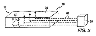
本発明の機能を組み入れた非限定的な表示パネル10は、図1から3に図示される。図1および2において最もよく分かるように、表示パネル10は、図示される非限定的な実施形態において、第1の主要表面(前面)14、第2の主要表面(裏面)16、前端18、後端20、左端22、および右端24を有する矩形基板12として示される、基板12を含む。図示される実施形態では、基板12の第1の主要表面14は、可視表面26を備える。基板軸28は、少なくとも部分的に基板12を貫通し、基板軸28の少なくとも一部は、可視表面26と略平行である。本発明は、矩形基板の使用に限定されず、いくつか例を挙げると、球形、正方形、円錐形、ピラミッド形、楕円形、または円筒形等を含むが、それらに限定されない、任意の基板形状を使用可能であることを理解されたい。さらに、基板12の対向する表面または端は、必ずしも互いに平行である必要はない。表示パネル10は、以下にさらに詳述されるように、1つ以上のエネルギ指向機能30を含む。機能30は、1つ以上の所定の方向、例えば、可視表面(viewing surface)26へ、電磁放射、例えば、可視光を選択的または優先的に指向するように構成される。
A
本発明の広範囲の実践において、表示パネル10の基板12は、任意の所望の特徴を有する任意の所望の材料であることが可能である。例えば、基板12は、可視光に対し透明または半透明であることが可能である。「透明」とは、0%を上回り、100%未満の可視光透過率を有することを意味する。別様に、基板12は、半透明であることが可能である。「半透明」とは、観察者と反対側の物体が明確に視認できないように、電磁エネルギ(例えば、可視光)を通過させるが、本エネルギを拡散させることを意味する。好適な材料の実施例として、プラスチック基板(ポリアクリル酸塩等のアクリルポリマー;メタクリル酸ポリメチル、メタクリル酸ポリエチル、メタクリル酸ポリプロピル等のメタクリル酸ポリアクリル;ポリウレタン;ポリカーボネート;ポリエチレンテレフタレート(PET)、ポリプロピレンテレフタレート、ポリブチレンテレフタレート等のポリアルキルテレフタレート;ポリシロキサン含有ポリマー;またはこれらを調製するための任意のモノマーの共重合体、あるいはそれらの任意の混合物)、セラミック基板、ガラス基板、あるいは上述のいずれかの混合物または組み合わせを含むが、それらに限定されない。例えば、基板12は、従来のソーダ石灰ケイ酸ガラス、ホウケイ酸ガラス、または鉛枠を含むことが可能である。ガラスは、クリアガラスであることが可能である。「クリアガラス」とは、非染色または非着色ガラスを意味する。別様に、ガラスは、染色または着色されたガラスであることが可能である。ガラスは、焼鈍または熱処理ガラスであることが可能である。本明細書に使用されるように、用語「熱処理」とは、硬度調整または少なくとも部分的に硬度調整されることを意味する。ガラスは、従来のフロートガラス等の任意の種類であることが可能であって、例えば、可視光線透過率、紫外線透過率、赤外線透過率、および/または総太陽エネルギ透過率の任意の値等の光特性を有する任意の組成であることが可能である。「フロートガラス」とは、溶融ガラスが、溶融金属浴上に成膜され、制御可能に冷却され、フロートガラスリボンを形成する、従来のフロートプロセスによって形成されるガラスを意味する。次いで、リボンは、所望に応じて、切断および/または成形および/または熱処理される。フロートガラスプロセスの実施例は、米国特許第4,466,562号および第4,671,155号に開示される。本発明を限定することなく、基板12の好適なガラスの実施例は、米国特許第4,746,347号、第4,792,536号、第5,030,593号、第5,030,594号、第5,240,886号、第5,385,872号、および第5,393,593号に記載される。基板12は、任意の所望の寸法、例えば、長さ、幅、形状、または厚さであることが可能である。一例示的非限定的な実施形態では、基板12は、1mm〜10mm厚、例えば、1mm〜5mm、または1.5mm〜2.5mm、あるいは1.8mm〜2.3mm厚であることが可能である。
In the broad practice of the present invention, the
一例示的非限定的な実施形態では、基板12は、参照波長550ナノメートル(nm)で、高可視光透過率を有することが可能である。「高可視光透過率」とは、87%以上、90%以上、91%以上、92以上等、550nmで85%以上の可視光透過率を意味する。本発明の実践に有用な非限定的な高可視光透過率ガラスは、米国特許第5,030,593号および第5,030,594号に開示され、Starphire(登録商標)の商標の下、PPG Industries,Inc.から市販されている。
In one exemplary non-limiting embodiment, the
一例示的非限定的な実施形態では、機能30は、基板材料と異なる屈折率を有する。屈折率の差異は、任意の所望の方法で達成されることが可能である。一例示的非限定的な実施形態では、機能30は、(1)異なる密度、例えば、そのすぐ近傍を囲む基板よりも高い密度を有する、(2)そのすぐ近傍を囲む基板と異なる組成を有する、または(3)そのすぐ近傍を囲む基板と機械的に異なり、例えば、局所応力領域を有する、および/または基板内に割れ目を含む、ことが可能である。本明細書で使用されるように、「すぐ近傍」は、1,000マイクロメータ未満、500マイクロメータ未満、200マイクロメータ未満等、機能30から10ミクロン〜1ミリメータ離れた距離を示す。機能30は、周囲基板12とは異なる屈折率を有することが可能である。一例示的非限定的な実施形態では、機能30は、異なる屈折率、例えば、周囲材料よりも高い屈折率を有することが可能である。例えば、機能30は、少なくとも0.002異なる屈折率、例えば、そのすぐ近傍を囲む基板12の屈折率よりも0.004、0.006、0.008、0.01、0.02、0.03、0.05、0.07、0.09、0.1、0.2、0.3、0.5、0.7、0.9、1.0高い、周囲材料よりも高い屈折率を有することが可能である。機能30と周囲材料との間の屈折率の変化は、漸進的または急激であることが可能である。離散的機能(図1から2Aに記載のような)に対し、屈折率の変化は、図3に示される連続的機能30に対するよりも漸次的であることが可能である(そこでは、連続的機能からの電磁エネルギの「漏出」を防止または低減するために、屈折率のより急激な変化が望ましい)。
In one exemplary non-limiting embodiment, function 30 has a different refractive index than the substrate material. The refractive index difference can be achieved in any desired manner. In one exemplary non-limiting embodiment, function 30 has (1) a different density, eg, a higher density than the substrate surrounding it, and (2) a different composition than the substrate surrounding it. Or (3) mechanically different from the substrate immediately surrounding it, eg having a local stress region and / or including cracks in the substrate. As used herein, “immediately” refers to a distance of 10 microns to 1 millimeter away from
ガラス基板12に対し、上記(1)が該当する場合、機能30は、ガラス製であり、異なる、例えば、そのすぐ近傍におけるガラスよりも高い密度を有することが可能である。上記(2)が該当する場合、機能30は、例えば、ナトリウム原子がガラス内に侵入し、機能30から離脱する結果生じ得る、ガラス基板12のバルク内のシリカネットワークの重合によってもたらされることが可能である。上記(3)が該当する場合、局所応力および/または割れ目が、ガラス基板12内に形成され、基板12内に新しいインターフェースを生成することが可能である。
When (1) above applies to the
本発明によると、機能30は、任意の形状であることが可能であり、種々の機能30は、同一または異なる形状であることが可能である。図1および2に示される非限定的な実施形態では、機能30は、400ナノメートル〜1ミリメータ、例えば、1ミクロン〜5ミクロンの範囲の長さ(側面から見る)を有する。各機能30は、同一または異なるサイズを有することが可能である。図1および2に示される実施形態は、複数の離間した個別の機能30を利用する。図1では、機能30の少なくともいくつかは、一列に配列される(平面内で)。図2および2Aでは、機能30の少なくともいくつかは、異なる列に配列される(すなわち、異なる平面)。表示パネル10は、1つ以上の平面において、1つ以上の配向を有する機能30を含むことが可能である。図3に示される実施形態では、機能30は、少なくとも部分的に基板12を貫通し、第1の先端32および第2の先端34を有する導波管または導管の形状をとる。図3の機能は、円形、楕円形、多角形(例えば、正方形、三角形等)等の任意の所望の断面を備えた管状の形状を有することが可能である。第1および第2の先端32、34は、基板12の表面の1つで終端する必要はないが、基板12内で開始および終了することが可能である。
According to the present invention, the
本発明の表示パネル10を作製する例示的方法が、初めに図4を参照して説明され、次いで、表示パネル10の種々の実施形態の動作について説明される。本発明の表示装置を作製するための例示的装置40は、図4に示される。装置40は、基板12を保持し、固定するための保持装置42を含む。装置40は、さらにレーザ44および集光レンズ46を含む。随意に、装置40は、従来のプリズム48をさらに含む、または利用することが可能である。水等の屈折率整合流体のフィルム51は、プリズム48と基板12の表面との間に位置されることが可能である。
An exemplary method of making the
レーザ44は、従来のナノ秒、ピコ秒、またはフェムト秒パルス状レーザ等を含むが、それらに限定されない、従来のパルス状レーザであることが可能である。好適なレーザとして、例えば、近赤外領域の波長を有するチタンドープサファイアレーザまたはイットリウムアルミニウムガーネット(YAG)レーザを含むが、それらに限定されない。特に好適なレーザとして、280nm〜1560nm、700nm〜1,064nmの範囲の波長、100フェムト秒〜5ナノ秒の範囲のパルス時間、および1〜5ミリジュールの範囲の電力を有する、パルス状レーザを含む。
The
レンズ46は、10×〜20×顕微鏡対物レンズ等を含むが、それに限定されない、任意の従来のレンズであることが可能である。レンズ46は、レーザ44によって放電される電磁放射に対し高い透明性を有することが可能である。
The
基板12およびレーザ44は、互いに対し移動可能である。例えば、図示される実施形態では、保持装置42は、レーザ44に対し任意の方向に基板12を移動するために使用することが可能な移動装置50を含む。しかしながら、レーザ44、集光レンズ46、プリズム48アセンブリが、基板12よりも移動可能であることは、同様に考えられる。
The
基板12に機能30を形成するために、レーザ44の焦点が基板12の内部にあるように、装置40は調整される。レーザ44が励起されると、電磁放射は、集光レンズ46をおよびプリズム48を通過し、基板12に入射する。プリズム48は、レーザ44が基板表面に対しある角度をなして向けられる場合生じ得る反射損の低減を支援する。油等の屈折率整合流体は、プリズム48と基板12との間に配置されることが可能である。焦点において、例えば、基板材料の密度および/または光特性を変更することにより、電磁放射によって、機能30が形成される。図4から理解されるように、レーザ44が、基板12の表面に対し角度52で配置されるため、機能30の長手方向軸54もまた、機能30を通過する基板平面58から類似の角度56オフセットされる。1つの機能30が形成された後、移動装置50が駆動され、基板12を移動させ、基板12内部のレーザ44の焦点を再配置することが可能である。次いで、レーザ44が再び駆動され、別の機能30を基板12に形成可能である。基板12が平面58に沿って単に平行移動される場合、図1に示されるような構造がもたらされる。基板12に対するレーザ44の角度に基づいて、機能30は、典型的には、例えば、400nm〜1mm、400nm〜300ミクロン、400nm〜200ミクロン、400nm〜100ミクロン、400nm〜50ミクロン、400nm〜10ミクロン、400nm〜5ミクロン、400nm〜1ミクロンの範囲の直径(楕円形の場合、縦軸)を有する楕円形または円形形状となる。理解されるように、機能30の直径が小さく、基板12の単位面積当たりの機能30が少ない程、機能30は、肉眼に対し見えにくくなる。
To form the
基板12が平面58の方向に平行移動されるが、レーザ44からの距離も変化する場合、図2に示されるような構造が形成されることが可能である。基板12が平行移動され、かつ回転または旋回される場合、図2Aに示されるような構造が形成されることが可能である。
If the
別様に、装置40を使用して、図3に示されるような円筒形または管形状の機能30を形成することが可能である。円筒形機能30は、直線または湾曲し、光チャネルあるいは導波管のような作用をすることが可能である。当業者に理解されるように、管状機能30を形成するために、基板12は、図4に示されるような類似方法で配置されることが可能である。レーザ44の焦点は、基板12および駆動されるレーザ44の端部またはその近傍(下端等)に配置可能である。レーザ44が駆動(例えば、波動)されている間、移動装置50を使用して、基板12を徐々にまたは漸次的に移動させ、レーザ44の焦点の位置を調節し、図3に示される管状機能30を形成することが可能である。
Alternatively, the
次に、本発明による表示パネル10の種々の非限定的な実施形態の動作が説明される。図1を参照すると、機能30は、基板12に形成され、照射される場合にパターンまたはイメージを形成するように配置される。例えば、図5aは、表示パネル10が照射されない場合の表示パネル10の可視表面26を示す。機能30は、検出されない、または肉眼で見てわずかに検出可能であってもよい。これは、小型の機能30によるためである。しかしながら、図1に戻ると、電磁放射源(例えば、光源60)が駆動され、基板12に指向されると、例えば、基板12の右端24では、光源60からの電磁放射62の少なくとも一部は、基板12の内部に指向される。
The operation of various non-limiting embodiments of the
図1から理解され得るように、電磁放射62が機能30に接触すると、機能30と衝突する放射62の少なくとも一部は、可視表面26へのその原経路から再指向される。このように、機能30は、電磁放射62の経路を反射または再指向する小型の鏡のように作用する。図5bは、光源60が照射され、基板12に配列された機能30から反射された放射により形成されるイメージを表す場合の、表示パネル10の可視表面26を示す。
As can be seen from FIG. 1, when the
図2に示される実施形態は、主として可視表面26へ放射62を指向する類似の方法で作用する。しかしながら、図2Aに示される実施形態では、放射62は、いくつかの異なる方向に指向される。
The embodiment shown in FIG. 2 operates in a similar manner that primarily directs
図3に示される実施形態は、上述と類似の方法で作用することが可能である。つまり、光源60は、細長い機能30の第1の先端32に隣接して配置される。光源60が駆動されると、光源60からの電磁放射62は、第1の先端32を通過し、機能30に入射し、第1の先端32から第2の先端34へ指向される。機能30と周囲ガラスとの屈折率の差異のため、機能30に入射する光は、ガラス基板内へ後方反射されず、むしろ機能30内に留まる。
The embodiment shown in FIG. 3 can work in a similar manner as described above. That is, the
本発明の広範囲の側面では、機能30は、三次元であることが可能であり、任意の縦横比を有することが可能である。各機能30は、同一または異なる縦横比を有することが可能である。機能30は、基板12の表面に対し任意の角度で配向されることが可能である。種々の機能30は、同一または異なる角度で配向されることが可能である。例えば、1つ以上の機能30は、イメージが表示される基板12の表面26に対し、角度45°で配向されることが可能である。基板内の単位面積当たりの機能30の数は、任意の方法で変更可能である。
In a broad aspect of the invention, the
本発明によると、基板12の1つ以上の表面が照射されると、イメージは、基板12の少なくとも1つの表面を通して見ることが可能である。上述のように、基板の表面の1つ以上を照射するステップは、エッジ照明を含む。非限定的な実施形態では、イメージは、基板12の他の表面上よりもある表面上でより可視的となることが可能である(すなわち、イメージは、基板12の他の表面よりもある表面上でより強烈である)。基板12の機能30が、無作為の指向とは対照的に、照射される光を優先的にある方向に再指向させるように設計される場合に、本効果は生じることが可能である。
According to the present invention, when one or more surfaces of the
一例示的非限定的な実施形態では、機能30は、機能30に衝突する光源60からの光を主としてある方向に再指向する。「主として」とは、例えば、再指向される光のうちの75%を超える光、または再指向される光のうちの85%を超える光等、再指向される光のうちの50%を超える光が、所定のある方向に向かうことを意味する。言い換えると、光は、全方向に等方的ではなく、所定の方法で異方的に指向される。別様に、図2Aから理解されるように、機能30をグループ化し、いくつかの異なる方向に光を再指向することが可能である。例えば、機能30のあるグループは、第1の方向に光を再指向し、機能30の別のグループは、異なる方向に光を再指向することが可能である。
In one exemplary non-limiting embodiment, function 30 redirects light from
表示パネル10によって表示可能なイメージの種類に関し、限定はない。例えば、イメージは、その形態において、単語、種々の形状、ロゴ、シンボル等であることが可能である。様々な着色された光源60を使用することによって、基板12を通して、種々の色を表示することが可能である。
There are no limitations on the types of images that can be displayed by the
非限定的な実施形態では、基板12のどの表面が照射されるかに応じて、異なるイメージが基板12に表示される。例えば、基板12のある表面が照射されると、「NO」が表示され、別の表面が照射されると、「YES」が表示されることが可能である。
In a non-limiting embodiment, different images are displayed on the
別の非限定的な実施形態では、基板12の複数の表面が、様々な着色された光源60によって同時に照射され、多彩色イメージを表示することが可能である。別様に、異なる機能30は、異なる波長の電磁放射を優先的に反射することが可能である。このように、同一光源によって照射される複数の機能30は、多彩色を指向または反射することが可能である。
In another non-limiting embodiment, multiple surfaces of the
本発明によると、基板内の機能30は、基板12の1つ以上の表面が照射されると、1つ以上の特定の方向に光を指向可能であるため、表示パネル10を使用して、種々の目的のために光を再指向することが可能である。例えば、表示パネル10は、部屋の中の特定の方向に太陽光を再指向するために使用される天窓であることが可能である。
According to the present invention, the
本発明によると、基板の表面を照射するための光源60は、基板に所望のメッセージ、標識、ロゴ、広告等を提供するために使用され得る、任意の光源であることが可能である。別様に、光源60は、赤外線(IR)および/または紫外線(UV)波長範囲等の非可視波長領域の電磁放射を提供可能であり、機能30は、これらの非可視領域内のみで放射を反射し、肉眼では非可視であるが、好適なフィルタ、レンズ、または受像機で検出され得るイメージを形成するように構成されることが可能である。好適な光源として、可視波長レーザ、ハロゲンおよび白熱ランプ、種々の色のLED、IR放射源、UV放射源等を含むが、それらに限定されない。表面の照射は、光源60から直接、または、例えば、光源60に近接する光ファイバから間接的に行うことが可能である。間接的に表面を照射するステップによって、光源60が物品から一定の距離で配置されることが可能になる。
According to the present invention, the
非限定的な実施形態では、好適な光源は、自然光、例えば、太陽の直接光線である。 In a non-limiting embodiment, a suitable light source is natural light, for example direct sunlight.
本発明の物品は、種々の方法で使用されることが可能である。例えば、センターハイマウントストップランプ(center high mounted stop lamp;CHMSL)、方向指示器等の信号装置、またはヘッドアップ表示装置(HUD)として、本物品を車両内で使用することが可能である。また、本発明の物品は、例えば、ガラス層にロゴ等のシンボルを表示するためのレストランの標識として使用することが可能である。 The articles of the present invention can be used in various ways. For example, the article can be used in a vehicle as a signal device such as a center high mounted stop lamp (CHMSL), a direction indicator, or a head-up display device (HUD). The article of the present invention can be used as a restaurant sign for displaying a symbol such as a logo on a glass layer.
非限定的な実施形態では、本発明の物品は、光活性要素を含有する、または光起電装置のカバーとしての基板に含めることが可能である。本発明の物品は、光活性要素によって生成されるエネルギの量を増加させるために、光を光活性要素に再指向する。別の非限定的な実施例として、本発明の物品は、窓内に存在し、自然光をあまり受光できない領域等の照明目的として、部屋の特定の領域に光を再指向する。 In a non-limiting embodiment, the article of the invention can be included in a substrate that contains a photoactive element or as a cover for a photovoltaic device. The articles of the present invention redirect light to the photoactive element to increase the amount of energy generated by the photoactive element. As another non-limiting example, the article of the present invention redirects light to a specific area of a room for illumination purposes, such as an area that resides in a window and is less susceptible to natural light.
別の潜在的非限定的な用途では、機能30は、強烈な光源が、特定の表面または端から表示パネル10を照射する場合に、光を強力に散乱させ、それによって、欠陥パターンを露呈し、表示パネル10背後のものを覆い隠させることが可能である。光源が、任意の他の表面または端から再指向される場合、仮に見える場合でも、欠陥パターンは、僅かに見えるだけとなる。強烈な光源がないと、欠陥パターンは、裸眼に対し完全または実質的に非可視となり得る。光源をオン/オフに切り替えることによって、ガラス背後のものを、遠隔で覆隠または露呈させることが可能である。
In another potential non-limiting application,
一例示的非限定的な実施形態では、本発明の装置は、照射される場合に、イメージを表示する必要はないが、むしろ、自然光等を含むが、それに限定されない、電磁放射等を1つ以上の所定の方向に再指向するために使用することが可能である。例えば、本発明の機能30は、窓、天窓等の建築的透明要素に組み込まれ、部屋の特定の部分へ太陽光を優先的に指向することが可能である。
In one exemplary non-limiting embodiment, the device of the present invention does not need to display an image when illuminated, but rather one electromagnetic radiation etc., including but not limited to natural light etc. It can be used to redirect in the above predetermined direction. For example, the
さらに、放射源60によって基板12に導入される光の波長を選択し、基板材料の特性の透過率に一致または補完させることが可能である。例えば、基板材料が、緑色光を透過するが、青色光または赤色光を遮断あるいは吸収する場合、緑色光を放出するように構成された放射源60を使用することが可能である。つまり、基板12に対し最も透明な波長または波長領域に一致する放射源60を選択することが可能である。別様に、基板12の組成を選択し、透過に望ましい波長に補完または一致させることが可能である。基板材料または組成を選択し、1つ以上の望ましくない波長を吸収または遮断(例えば、フィルタ)し、1つ以上の望ましい波長を透過させることが可能である。
Furthermore, the wavelength of light introduced into the
上述の説明に開示された概念から逸脱することなく、本発明に修正をなし得ることは、当業者には容易に理解されるであろう。そのような修正は、本発明の範囲内で含まれるものとみなされる。従って、上記本明細書に詳述された特定の実施形態は、例示にすぎず、本発明の範囲を限定するものではなく、本発明の範囲は、添付の請求の範囲の全範囲およびその同等物に対して与えられる。 It will be readily appreciated by those skilled in the art that modifications may be made to the invention without departing from the concepts disclosed in the foregoing description. Such modifications are considered to be included within the scope of the present invention. Accordingly, the specific embodiments detailed in the specification above are illustrative only and are not intended to limit the scope of the invention, which is intended to cover the full scope of the appended claims and equivalents thereof. Given to things.
Claims (17)
電磁放射を該基板内に導入するように構成された電磁放射源と、
該基板内の少なくとも1つの放射指向構造部材であって、該基板の材料とは異なる屈折率を有し、該電磁放射源によって該基板内に導入された電磁放射の少なくとも一部を所定の方向に再指向するように構成されており、該放射指向構造部材から反射された放射が、該基板の少なくとも1つの表面を通して可視である所定のイメージを形成するようなパターンで該少なくとも1つの放射指向構造部材が配置されている構造部材と
を含み、
ここで、該放射指向構造部材が、そのすぐ近傍にある該基板とは異なる密度を有する構造部材およびそのすぐ近傍の該基板と異なる組成を有する構造部材から選択され、
該放射指向構造部材が、第1の先端および第2の先端を有する円筒形状または管形状を有し、該放射指向構造部材が、湾曲しており、電磁放射を該第1の先端から該第2の先端へと指向させ、光チャネルまたは導波管のように作用する、装置。 A substrate made of plastic, ceramic or glass, the substrate being transparent or translucent to visible light; and
An electromagnetic radiation source configured to introduce electromagnetic radiation into the substrate;
At least one radiation directing structural member in the substrate having a refractive index different from that of the material of the substrate, wherein at least part of the electromagnetic radiation introduced into the substrate by the electromagnetic radiation source in a predetermined direction Wherein the radiation reflected from the radiation directing structural member forms a predetermined image that is visible through at least one surface of the substrate. and a structural member structural member is disposed viewed including,
Wherein the radiation directing structural member is selected from a structural member having a density different from that of the substrate immediately adjacent thereto and a structural member having a composition different from that of the substrate immediately adjacent thereto,
The radiation directing structural member has a cylindrical or tube shape having a first tip and a second tip, the radiation directing structural member is curved, and electromagnetic radiation is transmitted from the first tip to the first. A device that is directed to the tip of two and acts like an optical channel or waveguide .
電磁放射を該基板内に導入するように構成された電磁放射源と、
該基板内の少なくとも1つの放射指向構造部材であって、該基板の材料とは異なる屈折率を有し、該電磁放射源によって該基板内に導入された電磁放射の少なくとも一部を該可視表面へ再指向するように構成されており、該放射指向構造部材から反射された放射が、該基板の少なくとも1つの表面を通して可視である所定のイメージを形成するようなパターンで該少なくとも1つの放射指向構造部材が配置されている構造部材と
を含み、
ここで、該放射指向構造部材が、そのすぐ近傍にある該基板とは異なる密度を有する構造部材およびそのすぐ近傍の該基板と異なる組成を有する構造部材から選択され、
該放射指向構造部材が、第1の先端および第2の先端を有する円筒形状または管形状を有し、該放射指向構造部材が、湾曲しており、電磁放射を該第1の先端から該第2の先端へと指向させ、光チャネルまたは導波管のように作用する、表示装置。 A substrate made of plastic, ceramic or glass having a visible surface and transparent or translucent to visible light;
An electromagnetic radiation source configured to introduce electromagnetic radiation into the substrate;
At least one radiation directing structural member in the substrate having a different refractive index than the material of the substrate, and at least a portion of the electromagnetic radiation introduced into the substrate by the electromagnetic radiation source in the visible surface The at least one radiation directing in a pattern such that radiation reflected from the radiation directing structural member forms a predetermined image that is visible through at least one surface of the substrate. and a structural member structural member is disposed viewed including,
Wherein the radiation directing structural member is selected from a structural member having a density different from that of the substrate immediately adjacent thereto and a structural member having a composition different from that of the substrate immediately adjacent thereto;
The radiation directing structural member has a cylindrical or tube shape having a first tip and a second tip, the radiation directing structural member is curved, and electromagnetic radiation is transmitted from the first tip to the first. A display device that is directed to the tip of 2 and acts like an optical channel or waveguide .
該基板内の複数の放射指向構造部材であって、該基板の材料とは異なる屈折率を有する構造部材と、
電磁放射を該基板内に導入するように構成された電磁放射源と
を含み、該放射指向構造部材は、該電磁放射源によって該基板内に導入された該電磁放射の少なくとも一部を、該可視表面へ再指向するように構成され、該放射指向構造部材から反射された放射が、該基板の少なくとも1つの表面を通して可視である所定のイメージを形成するようなパターンで該放射指向構造部材が配置されており、
ここで、該放射指向構造部材が、そのすぐ近傍にある該基板とは異なる密度を有する構造部材およびそのすぐ近傍の該基板と異なる組成を有する構造部材から選択され、
該放射指向構造部材が、第1の先端および第2の先端を有する円筒形状または管形状を有し、該放射指向構造部材が、湾曲しており、電磁放射を該第1の先端から該第2の先端へと指向させ、光チャネルまたは導波管のように作用する、表示装置。 A substrate made of plastic, ceramic or glass having a visible surface and transparent or translucent to visible light;
A plurality of radiation directing structural members in the substrate, the structural members having a refractive index different from the material of the substrate;
An electromagnetic radiation source configured to introduce electromagnetic radiation into the substrate, the radiation directing structural member at least part of the electromagnetic radiation introduced into the substrate by the electromagnetic radiation source, is configured to redirect the visible surface, radiation reflected from the radiation directivity structural members, is the radiation directivity structural member in a pattern as to form a predetermined image is visible through at least one surface of the substrate Has been placed ,
Wherein the radiation directing structural member is selected from a structural member having a density different from that of the substrate immediately adjacent thereto and a structural member having a composition different from that of the substrate immediately adjacent thereto;
The radiation directing structural member has a cylindrical or tube shape having a first tip and a second tip, the radiation directing structural member is curved, and electromagnetic radiation is transmitted from the first tip to the first. A display device that is directed to the tip of 2 and acts like an optical channel or waveguide .
ここで、該放射指向構造部材が、そのすぐ近傍にある該基板とは異なる密度を有する構造部材およびそのすぐ近傍の該基板と異なる組成を有する構造部材から選択され、
該放射指向構造部材が、第1の先端および第2の先端を有する円筒形状または管形状を有し、該放射指向構造部材が、湾曲しており、電磁放射を該第1の先端から該第2の先端へと指向させ、光チャネルまたは導波管のように作用する、方法。 A refractive index different from the material of the substrate, which is configured to focus the radiation beam into a substrate made of plastic, ceramic or glass and redirect the radiation introduced into the substrate in a predetermined direction. Forming a radiation directing structure having a substrate, wherein the substrate is transparent or translucent to visible light, and the radiation reflected from the radiation directing structure is The at least one radiation directing structural member is arranged in a pattern to form a predetermined image that is visible through at least one surface of the substrate ;
Wherein the radiation directing structural member is selected from a structural member having a density different from that of the substrate immediately adjacent thereto and a structural member having a composition different from that of the substrate immediately adjacent thereto;
The radiation directing structural member has a cylindrical or tube shape having a first tip and a second tip, the radiation directing structural member is curved, and electromagnetic radiation is transmitted from the first tip to the first. A method that is directed to the tip of two and acts like an optical channel or waveguide .
Applications Claiming Priority (3)
| Application Number | Priority Date | Filing Date | Title |
|---|---|---|---|
| US75837606P | 2006-01-12 | 2006-01-12 | |
| US60/758,376 | 2006-01-12 | ||
| PCT/US2007/000776 WO2007082045A1 (en) | 2006-01-12 | 2007-01-12 | Display panel having laser induced light redirecting features |
Publications (2)
| Publication Number | Publication Date |
|---|---|
| JP2009524082A JP2009524082A (en) | 2009-06-25 |
| JP5317704B2 true JP5317704B2 (en) | 2013-10-16 |
Family
ID=37908052
Family Applications (1)
| Application Number | Title | Priority Date | Filing Date |
|---|---|---|---|
| JP2008550417A Active JP5317704B2 (en) | 2006-01-12 | 2007-01-12 | Display panel having function of redirecting light introduced by laser |
Country Status (13)
| Country | Link |
|---|---|
| US (1) | US8547008B2 (en) |
| EP (1) | EP1979889B1 (en) |
| JP (1) | JP5317704B2 (en) |
| KR (1) | KR101064859B1 (en) |
| CN (1) | CN101390143B (en) |
| AU (1) | AU2007204856B2 (en) |
| BR (1) | BRPI0706514A2 (en) |
| CA (1) | CA2637002C (en) |
| DK (1) | DK1979889T3 (en) |
| ES (1) | ES2383915T3 (en) |
| IL (1) | IL192721A (en) |
| RU (1) | RU2444795C2 (en) |
| WO (1) | WO2007082045A1 (en) |
Families Citing this family (14)
| Publication number | Priority date | Publication date | Assignee | Title |
|---|---|---|---|---|
| US8629610B2 (en) * | 2006-01-12 | 2014-01-14 | Ppg Industries Ohio, Inc. | Display panel |
| CN101390143B (en) | 2006-01-12 | 2012-09-05 | Ppg工业俄亥俄公司 | Display panel having laser induced light redirecting features |
| US7974508B2 (en) | 2009-02-03 | 2011-07-05 | Nitto Denko Corporation | Multi-layer structure and method for manufacturing the same |
| DE102009007198A1 (en) * | 2009-02-03 | 2010-08-12 | GM Global Technology Operations, Inc., Detroit | Vehicle with dashboard and display device for the dashboard and a method of manufacturing the display device |
| EP2214040A1 (en) | 2009-02-03 | 2010-08-04 | Nitto Denko Corporation | Multi-Layer Structure and Method for Manufacturing the Same |
| WO2010090600A1 (en) * | 2009-02-03 | 2010-08-12 | Nitto Denko Corporation | Multi-layer structure and method for manufacturing the same |
| JP6229263B2 (en) * | 2011-12-12 | 2017-11-15 | 三菱ケミカル株式会社 | Method for manufacturing light guide for surface light source device |
| EP2765353B1 (en) * | 2013-02-06 | 2018-11-07 | Hartmut S. Engel | Lamp with a Light conducting disc assembly |
| PL3033745T3 (en) * | 2013-09-17 | 2017-12-29 | Philips Lighting Holding B.V. | A lighting device |
| TWI641874B (en) | 2014-01-29 | 2018-11-21 | 美商康寧公司 | Laser featured glass for display illumination |
| DE202015009023U1 (en) | 2015-06-19 | 2016-07-18 | Laser- Und Medizin- Technologie Gmbh | Lateral radiating optical fibers |
| CN105445933B (en) * | 2015-12-22 | 2018-06-26 | 中国科学院长春光学精密机械与物理研究所 | A kind of high-resolution moon edge optical image-forming objective lens |
| TW201733802A (en) * | 2016-01-05 | 2017-10-01 | 康寧公司 | Laminated light diffusing optical fiber |
| WO2019077589A1 (en) * | 2017-10-20 | 2019-04-25 | Ecole Polytechnique Federale De Lausanne (Epfl) | Multi-spectral image priniting method |
Family Cites Families (83)
| Publication number | Priority date | Publication date | Assignee | Title |
|---|---|---|---|---|
| NL126968C (en) | 1957-05-03 | 1900-01-01 | ||
| US3843346A (en) | 1973-03-06 | 1974-10-22 | Ppg Industries Inc | Manufacture of sheet glass by continuous float process |
| JPS5524632Y2 (en) * | 1974-06-07 | 1980-06-12 | ||
| US4092518A (en) * | 1976-12-07 | 1978-05-30 | Laser Technique S.A. | Method of decorating a transparent plastics material article by means of a laser beam |
| US4466562A (en) | 1981-12-15 | 1984-08-21 | Ppg Industries, Inc. | Method of and apparatus for severing a glass sheet |
| US4671155A (en) | 1985-06-13 | 1987-06-09 | Ppg Industries, Inc. | Positioning apparatus |
| US4746347A (en) | 1987-01-02 | 1988-05-24 | Ppg Industries, Inc. | Patterned float glass method |
| US4792536A (en) | 1987-06-29 | 1988-12-20 | Ppg Industries, Inc. | Transparent infrared absorbing glass and method of making |
| JP2814684B2 (en) * | 1990-04-16 | 1998-10-27 | 住友電気工業株式会社 | Luminescent plate |
| US5030593A (en) | 1990-06-29 | 1991-07-09 | Ppg Industries, Inc. | Lightly tinted glass compatible with wood tones |
| US5030594A (en) | 1990-06-29 | 1991-07-09 | Ppg Industries, Inc. | Highly transparent, edge colored glass |
| US5240886A (en) | 1990-07-30 | 1993-08-31 | Ppg Industries, Inc. | Ultraviolet absorbing, green tinted glass |
| IL99170A0 (en) * | 1990-08-15 | 1992-07-15 | United Distillers Plc | Method and apparatus for sub-surface marking |
| US5393593A (en) | 1990-10-25 | 1995-02-28 | Ppg Industries, Inc. | Dark gray, infrared absorbing glass composition and coated glass for privacy glazing |
| EP0495273B1 (en) * | 1991-01-16 | 1996-09-11 | Lumitex Inc. | Thin panel illuminator |
| US5287427A (en) | 1992-05-05 | 1994-02-15 | At&T Bell Laboratories | Method of making an article comprising an optical component, and article comprising the component |
| US5500031A (en) | 1992-05-05 | 1996-03-19 | At&T Corp. | Method for increasing the index of refraction of a glassy material |
| JP2644663B2 (en) | 1993-03-08 | 1997-08-25 | 工業技術院長 | Method of changing refractive index by light induction |
| DE69408021T2 (en) | 1993-04-30 | 1998-05-07 | At & T Corp | Process for increasing the refractive index of glass |
| US5637244A (en) | 1993-05-13 | 1997-06-10 | Podarok International, Inc. | Method and apparatus for creating an image by a pulsed laser beam inside a transparent material |
| GB2281129B (en) * | 1993-08-19 | 1997-04-09 | United Distillers Plc | Method of marking a body of glass |
| JPH0719775U (en) * | 1993-09-14 | 1995-04-07 | 筒中プラスチック工業株式会社 | Fluorescent display |
| JP3796775B2 (en) | 1994-10-17 | 2006-07-12 | 住友電気工業株式会社 | Method for increasing the refractive index of silica glass |
| US5707908A (en) | 1995-01-06 | 1998-01-13 | Nikon Corporation | Silica glass |
| US5684621A (en) | 1995-05-08 | 1997-11-04 | Downing; Elizabeth Anne | Method and system for three-dimensional display of information based on two-photon upconversion |
| US5647040A (en) | 1995-12-14 | 1997-07-08 | Corning Incorporated | Tunable optical coupler using photosensitive glass |
| JP3649835B2 (en) | 1996-03-18 | 2005-05-18 | 独立行政法人科学技術振興機構 | Optical waveguide fabrication method |
| SE510703C2 (en) | 1996-09-17 | 1999-06-14 | Optisk Forskning Inst | Optical organ and method of such organ |
| US6474107B1 (en) | 1996-12-02 | 2002-11-05 | Franklin W. Dabby | Fluorinating an optical fiber preform in a pure aluminum oxide muffle tube |
| JPH10232638A (en) * | 1997-02-19 | 1998-09-02 | Sugimoto Masafumi | Electric light device |
| JPH10265243A (en) | 1997-03-26 | 1998-10-06 | Rikagaku Kenkyusho | Control of refractive index of silica glass |
| US6432278B2 (en) | 1997-03-26 | 2002-08-13 | The Institute Of Physical And Chemical Research | Method for controlling refractive index of silica glass |
| US6392683B1 (en) * | 1997-09-26 | 2002-05-21 | Sumitomo Heavy Industries, Ltd. | Method for making marks in a transparent material by using a laser |
| JP3292294B2 (en) * | 1997-11-07 | 2002-06-17 | 住友重機械工業株式会社 | Marking method and marking device using laser |
| KR20010024394A (en) | 1997-10-02 | 2001-03-26 | 유니버시티 오브 로체스터 | Light-induced refractive index changes in low temperature glasses |
| JP3468450B2 (en) | 1998-07-17 | 2003-11-17 | 科学技術振興事業団 | Method for selective reforming inside solid material and solid material having selectively reformed inside |
| CA2369584A1 (en) | 1999-04-09 | 2000-10-19 | The University Of New Mexico | Large photosensitivity in lead silicate glasses |
| US6442311B1 (en) | 1999-07-09 | 2002-08-27 | Agere Systems Guardian Corp. | Optical device having modified transmission characteristics by localized thermal treatment |
| US6573026B1 (en) | 1999-07-29 | 2003-06-03 | Corning Incorporated | Femtosecond laser writing of glass, including borosilicate, sulfide, and lead glasses |
| KR20020038786A (en) | 1999-09-30 | 2002-05-23 | 알프레드 엘. 미첼슨 | Deep UV laser internally induced densification in silica glasses |
| DE29917623U1 (en) * | 1999-10-06 | 1999-12-16 | Reitter & Schefenacker Gmbh | Display or illumination element for motor vehicles |
| JP3531738B2 (en) * | 2000-02-22 | 2004-05-31 | 日本電気株式会社 | Refractive index correcting method, refractive index correcting apparatus, and optical waveguide device |
| DE10015702A1 (en) | 2000-03-29 | 2001-10-18 | Vitro Laser Gmbh | Method for introducing at least one internal engraving into a flat body and device for carrying out the method |
| US6333486B1 (en) * | 2000-04-25 | 2001-12-25 | Igor Troitski | Method and laser system for creation of laser-induced damages to produce high quality images |
| JP2002014246A (en) * | 2000-06-27 | 2002-01-18 | Matsushita Electric Works Ltd | Optical waveguide and method for manufacturing the same |
| JP3522670B2 (en) | 2000-08-28 | 2004-04-26 | 住友重機械工業株式会社 | Laser marking method |
| US6596967B2 (en) | 2000-10-24 | 2003-07-22 | Edward Miesak | Laser based etching device |
| DE10064742A1 (en) | 2000-12-22 | 2002-06-27 | Thomas Emde | Double-glazed window element with internal illumination provided by light sources incorporated in frame construction |
| US7075112B2 (en) * | 2001-01-31 | 2006-07-11 | Gentex Corporation | High power radiation emitter device and heat dissipating package for electronic components |
| US20020186924A1 (en) | 2001-02-22 | 2002-12-12 | Kohnke Glenn E. | Grating fabrication method and apparatus |
| JP4085155B2 (en) | 2001-02-23 | 2008-05-14 | 独立行政法人産業技術総合研究所 | Glass material having refractive index distribution and manufacturing method thereof |
| JP2003012346A (en) | 2001-06-27 | 2003-01-15 | Central Glass Co Ltd | Method for coloring plate glass |
| JP2003035809A (en) | 2001-07-25 | 2003-02-07 | Japan Science & Technology Corp | Binary lens and its manufacturing method |
| US6957904B2 (en) | 2001-07-30 | 2005-10-25 | 3M Innovative Properties Company | Illumination device utilizing displaced radiation patterns |
| US20030076487A1 (en) | 2001-08-03 | 2003-04-24 | Cannon Bret D. | System and method for glass processing and stress measurement |
| RU2216787C2 (en) * | 2001-09-27 | 2003-11-20 | Закрытое акционерное общество "Инел-агентство" | Image generation method |
| US20030099452A1 (en) | 2001-11-28 | 2003-05-29 | Borrelli Nicholas F. | Manipulating the size of waveguides written into substrates using femtosecond laser pulses |
| US6768080B2 (en) | 2001-12-17 | 2004-07-27 | Troitski | Method for production of laser-induced damage images with special characteristics by creating damages of special space shape |
| JP2003200700A (en) * | 2002-01-07 | 2003-07-15 | Masao Yoshida | Collective transparent object having outer surface marking part |
| US6670576B2 (en) * | 2002-04-08 | 2003-12-30 | Igor Troitski | Method for producing images containing laser-induced color centers and laser-induced damages |
| JP2003321252A (en) | 2002-04-25 | 2003-11-11 | Japan Science & Technology Corp | Process for forming phase-separated region inside glass |
| US6900941B2 (en) | 2002-05-16 | 2005-05-31 | Eastman Kodak Company | Light diffuser with colored variable diffusion |
| US6950591B2 (en) | 2002-05-16 | 2005-09-27 | Corning Incorporated | Laser-written cladding for waveguide formations in glass |
| JP4095358B2 (en) * | 2002-06-25 | 2008-06-04 | 日立電線株式会社 | Holy waveguide type optical circuit and manufacturing method thereof |
| JP2004046031A (en) * | 2002-07-16 | 2004-02-12 | Hitachi Cable Ltd | Filmy glass waveguide and manufacturing method therefor |
| CA2396831A1 (en) | 2002-08-02 | 2004-02-02 | Femtonics Corporation | Microstructuring optical wave guide devices with femtosecond optical pulses |
| JP3928042B2 (en) | 2002-09-26 | 2007-06-13 | 独立行政法人産業技術総合研究所 | Diffraction grating and manufacturing method thereof |
| JP4658605B2 (en) * | 2002-10-08 | 2011-03-23 | 日本カーバイド工業株式会社 | Retroreflective display |
| EP1408362A1 (en) * | 2002-10-10 | 2004-04-14 | FER Fahrzeugelektrik GmbH | Lamp, in particular vehicle lamp |
| JP2004196585A (en) * | 2002-12-18 | 2004-07-15 | Nippon Sheet Glass Co Ltd | Method for forming heterogeneous phase within material with laser beam, structure and optical parts |
| US6740846B1 (en) * | 2003-03-27 | 2004-05-25 | Igor Troitski | Method for production of 3D laser-induced head image inside transparent material by using several 2D portraits |
| JP2004361628A (en) * | 2003-06-04 | 2004-12-24 | Akashi Denki Kk | Illumination signboard |
| JP4257411B2 (en) | 2003-08-21 | 2009-04-22 | 独立行政法人産業技術総合研究所 | Glass material having refractive index distribution and manufacturing method thereof |
| JP2007504982A (en) | 2003-09-08 | 2007-03-08 | コニンクリユケ フィリップス エレクトロニクス エヌ.ブイ. | Daylight luminescent panel |
| GB0323922D0 (en) | 2003-10-11 | 2003-11-12 | Univ Aston | Laser inscription of optical structures in laser crystals |
| JP2005158370A (en) | 2003-11-21 | 2005-06-16 | Toyota Industries Corp | Planar light source device and liquid crystal display device |
| AT413891B (en) * | 2003-12-29 | 2006-07-15 | Austria Tech & System Tech | CIRCUIT BOARD ELEMENT WITH AT LEAST ONE LIGHT WAVEGUIDE, AND METHOD FOR PRODUCING SUCH A LADDER PLATE ELEMENT |
| JP2005205464A (en) * | 2004-01-23 | 2005-08-04 | Okamoto Glass Co Ltd | Laser beam machining method, structure and optical element |
| JP2005255512A (en) | 2004-02-13 | 2005-09-22 | Central Glass Co Ltd | Rare earth element-containing functional glass and its producing method |
| JP3108802U (en) * | 2004-09-29 | 2005-04-28 | 有限会社シミズテクノ | display |
| CN101390143B (en) | 2006-01-12 | 2012-09-05 | Ppg工业俄亥俄公司 | Display panel having laser induced light redirecting features |
| US7443284B2 (en) * | 2006-05-09 | 2008-10-28 | International Business Machines Corporation | Method and system for sending events between vehicles |
| US7972051B2 (en) | 2006-09-21 | 2011-07-05 | Motorola Mobility, Inc. | Double-sided backlight and assembly incorporating a double-sided light source coupling light guide |
-
2007
- 2007-01-12 CN CN2007800067584A patent/CN101390143B/en active Active
- 2007-01-12 US US11/653,141 patent/US8547008B2/en active Active
- 2007-01-12 CA CA2637002A patent/CA2637002C/en not_active Expired - Fee Related
- 2007-01-12 WO PCT/US2007/000776 patent/WO2007082045A1/en active Application Filing
- 2007-01-12 RU RU2008133029/13A patent/RU2444795C2/en not_active IP Right Cessation
- 2007-01-12 BR BRPI0706514-0A patent/BRPI0706514A2/en not_active IP Right Cessation
- 2007-01-12 EP EP07709711A patent/EP1979889B1/en active Active
- 2007-01-12 DK DK07709711.1T patent/DK1979889T3/en active
- 2007-01-12 KR KR1020087019619A patent/KR101064859B1/en active IP Right Grant
- 2007-01-12 JP JP2008550417A patent/JP5317704B2/en active Active
- 2007-01-12 AU AU2007204856A patent/AU2007204856B2/en not_active Ceased
- 2007-01-12 ES ES07709711T patent/ES2383915T3/en active Active
-
2008
- 2008-07-09 IL IL192721A patent/IL192721A/en not_active IP Right Cessation
Also Published As
| Publication number | Publication date |
|---|---|
| AU2007204856A1 (en) | 2007-07-19 |
| RU2444795C2 (en) | 2012-03-10 |
| CN101390143B (en) | 2012-09-05 |
| IL192721A (en) | 2013-03-24 |
| KR101064859B1 (en) | 2011-09-14 |
| CA2637002C (en) | 2012-05-15 |
| DK1979889T3 (en) | 2012-09-10 |
| US8547008B2 (en) | 2013-10-01 |
| CA2637002A1 (en) | 2007-07-19 |
| AU2007204856B2 (en) | 2011-03-31 |
| WO2007082045A1 (en) | 2007-07-19 |
| ES2383915T3 (en) | 2012-06-27 |
| IL192721A0 (en) | 2009-02-11 |
| KR20080091215A (en) | 2008-10-09 |
| JP2009524082A (en) | 2009-06-25 |
| US20070165976A1 (en) | 2007-07-19 |
| RU2008133029A (en) | 2010-02-20 |
| CN101390143A (en) | 2009-03-18 |
| EP1979889B1 (en) | 2012-05-23 |
| BRPI0706514A2 (en) | 2011-03-29 |
| EP1979889A1 (en) | 2008-10-15 |
Similar Documents
| Publication | Publication Date | Title |
|---|---|---|
| JP5317704B2 (en) | Display panel having function of redirecting light introduced by laser | |
| US11822113B2 (en) | Daylight responsive LED illumination panel with color temperature control | |
| JP5342016B2 (en) | Large area light panel and screen | |
| WO2003014777A3 (en) | Optical film having microreplicated structures | |
| ES2276783T5 (en) | Edge Lighting Device On | |
| JP2017507103A (en) | Glass for display lighting processed with laser | |
| US9651728B2 (en) | Variable index light extraction layer with microreplicated posts and methods of making the same | |
| KR20150052054A (en) | Illuminated glass panel | |
| US8629610B2 (en) | Display panel | |
| JP2012514835A (en) | Optical system for light guide with control output | |
| US10429553B2 (en) | Optical assembly having microlouvers | |
| CN102692670A (en) | Guide light board and manufacturing method thereof as well as lateral type backlight module applying light guide board | |
| CN100405155C (en) | Backlight module | |
| CN218819780U (en) | Back light plate | |
| TW201945168A (en) | Optical device | |
| TW201003223A (en) | Light-guiding structrure, light guide plate and backlight module having the same |
Legal Events
| Date | Code | Title | Description |
|---|---|---|---|
| A131 | Notification of reasons for refusal |
Free format text: JAPANESE INTERMEDIATE CODE: A131 Effective date: 20100713 |
|
| A601 | Written request for extension of time |
Free format text: JAPANESE INTERMEDIATE CODE: A601 Effective date: 20101012 |
|
| A602 | Written permission of extension of time |
Free format text: JAPANESE INTERMEDIATE CODE: A602 Effective date: 20101019 |
|
| A521 | Request for written amendment filed |
Free format text: JAPANESE INTERMEDIATE CODE: A523 Effective date: 20101111 |
|
| A131 | Notification of reasons for refusal |
Free format text: JAPANESE INTERMEDIATE CODE: A131 Effective date: 20110705 |
|
| A601 | Written request for extension of time |
Free format text: JAPANESE INTERMEDIATE CODE: A601 Effective date: 20111004 |
|
| A602 | Written permission of extension of time |
Free format text: JAPANESE INTERMEDIATE CODE: A602 Effective date: 20111012 |
|
| A601 | Written request for extension of time |
Free format text: JAPANESE INTERMEDIATE CODE: A601 Effective date: 20111104 |
|
| A602 | Written permission of extension of time |
Free format text: JAPANESE INTERMEDIATE CODE: A602 Effective date: 20111111 |
|
| A601 | Written request for extension of time |
Free format text: JAPANESE INTERMEDIATE CODE: A601 Effective date: 20111202 |
|
| A602 | Written permission of extension of time |
Free format text: JAPANESE INTERMEDIATE CODE: A602 Effective date: 20111209 |
|
| A521 | Request for written amendment filed |
Free format text: JAPANESE INTERMEDIATE CODE: A523 Effective date: 20111228 |
|
| A02 | Decision of refusal |
Free format text: JAPANESE INTERMEDIATE CODE: A02 Effective date: 20121128 |
|
| A521 | Request for written amendment filed |
Free format text: JAPANESE INTERMEDIATE CODE: A523 Effective date: 20130328 |
|
| A911 | Transfer to examiner for re-examination before appeal (zenchi) |
Free format text: JAPANESE INTERMEDIATE CODE: A911 Effective date: 20130419 |
|
| TRDD | Decision of grant or rejection written | ||
| A01 | Written decision to grant a patent or to grant a registration (utility model) |
Free format text: JAPANESE INTERMEDIATE CODE: A01 Effective date: 20130708 |
|
| A61 | First payment of annual fees (during grant procedure) |
Free format text: JAPANESE INTERMEDIATE CODE: A61 Effective date: 20130709 |
|
| R150 | Certificate of patent or registration of utility model |
Ref document number: 5317704 Country of ref document: JP Free format text: JAPANESE INTERMEDIATE CODE: R150 Free format text: JAPANESE INTERMEDIATE CODE: R150 |
|
| R250 | Receipt of annual fees |
Free format text: JAPANESE INTERMEDIATE CODE: R250 |
|
| S111 | Request for change of ownership or part of ownership |
Free format text: JAPANESE INTERMEDIATE CODE: R313113 |
|
| R350 | Written notification of registration of transfer |
Free format text: JAPANESE INTERMEDIATE CODE: R350 |
|
| R250 | Receipt of annual fees |
Free format text: JAPANESE INTERMEDIATE CODE: R250 |
|
| R250 | Receipt of annual fees |
Free format text: JAPANESE INTERMEDIATE CODE: R250 |
|
| R250 | Receipt of annual fees |
Free format text: JAPANESE INTERMEDIATE CODE: R250 |
|
| R250 | Receipt of annual fees |
Free format text: JAPANESE INTERMEDIATE CODE: R250 |