JP5307319B2 - Thin film transistor array panel and manufacturing method thereof - Google Patents
Thin film transistor array panel and manufacturing method thereof Download PDFInfo
- Publication number
- JP5307319B2 JP5307319B2 JP2006047707A JP2006047707A JP5307319B2 JP 5307319 B2 JP5307319 B2 JP 5307319B2 JP 2006047707 A JP2006047707 A JP 2006047707A JP 2006047707 A JP2006047707 A JP 2006047707A JP 5307319 B2 JP5307319 B2 JP 5307319B2
- Authority
- JP
- Japan
- Prior art keywords
- electrode
- thin film
- film transistor
- pixel electrode
- transistor array
- Prior art date
- Legal status (The legal status is an assumption and is not a legal conclusion. Google has not performed a legal analysis and makes no representation as to the accuracy of the status listed.)
- Active
Links
Images


Classifications
-
- G—PHYSICS
- G02—OPTICS
- G02F—OPTICAL DEVICES OR ARRANGEMENTS FOR THE CONTROL OF LIGHT BY MODIFICATION OF THE OPTICAL PROPERTIES OF THE MEDIA OF THE ELEMENTS INVOLVED THEREIN; NON-LINEAR OPTICS; FREQUENCY-CHANGING OF LIGHT; OPTICAL LOGIC ELEMENTS; OPTICAL ANALOGUE/DIGITAL CONVERTERS
- G02F1/00—Devices or arrangements for the control of the intensity, colour, phase, polarisation or direction of light arriving from an independent light source, e.g. switching, gating or modulating; Non-linear optics
- G02F1/01—Devices or arrangements for the control of the intensity, colour, phase, polarisation or direction of light arriving from an independent light source, e.g. switching, gating or modulating; Non-linear optics for the control of the intensity, phase, polarisation or colour
- G02F1/13—Devices or arrangements for the control of the intensity, colour, phase, polarisation or direction of light arriving from an independent light source, e.g. switching, gating or modulating; Non-linear optics for the control of the intensity, phase, polarisation or colour based on liquid crystals, e.g. single liquid crystal display cells
- G02F1/133—Constructional arrangements; Operation of liquid crystal cells; Circuit arrangements
- G02F1/136—Liquid crystal cells structurally associated with a semi-conducting layer or substrate, e.g. cells forming part of an integrated circuit
- G02F1/1362—Active matrix addressed cells
- G02F1/136286—Wiring, e.g. gate line, drain line
-
- G—PHYSICS
- G02—OPTICS
- G02F—OPTICAL DEVICES OR ARRANGEMENTS FOR THE CONTROL OF LIGHT BY MODIFICATION OF THE OPTICAL PROPERTIES OF THE MEDIA OF THE ELEMENTS INVOLVED THEREIN; NON-LINEAR OPTICS; FREQUENCY-CHANGING OF LIGHT; OPTICAL LOGIC ELEMENTS; OPTICAL ANALOGUE/DIGITAL CONVERTERS
- G02F1/00—Devices or arrangements for the control of the intensity, colour, phase, polarisation or direction of light arriving from an independent light source, e.g. switching, gating or modulating; Non-linear optics
- G02F1/01—Devices or arrangements for the control of the intensity, colour, phase, polarisation or direction of light arriving from an independent light source, e.g. switching, gating or modulating; Non-linear optics for the control of the intensity, phase, polarisation or colour
- G02F1/13—Devices or arrangements for the control of the intensity, colour, phase, polarisation or direction of light arriving from an independent light source, e.g. switching, gating or modulating; Non-linear optics for the control of the intensity, phase, polarisation or colour based on liquid crystals, e.g. single liquid crystal display cells
- G02F1/133—Constructional arrangements; Operation of liquid crystal cells; Circuit arrangements
- G02F1/1333—Constructional arrangements; Manufacturing methods
- G02F1/133345—Insulating layers
-
- G—PHYSICS
- G02—OPTICS
- G02F—OPTICAL DEVICES OR ARRANGEMENTS FOR THE CONTROL OF LIGHT BY MODIFICATION OF THE OPTICAL PROPERTIES OF THE MEDIA OF THE ELEMENTS INVOLVED THEREIN; NON-LINEAR OPTICS; FREQUENCY-CHANGING OF LIGHT; OPTICAL LOGIC ELEMENTS; OPTICAL ANALOGUE/DIGITAL CONVERTERS
- G02F1/00—Devices or arrangements for the control of the intensity, colour, phase, polarisation or direction of light arriving from an independent light source, e.g. switching, gating or modulating; Non-linear optics
- G02F1/01—Devices or arrangements for the control of the intensity, colour, phase, polarisation or direction of light arriving from an independent light source, e.g. switching, gating or modulating; Non-linear optics for the control of the intensity, phase, polarisation or colour
- G02F1/13—Devices or arrangements for the control of the intensity, colour, phase, polarisation or direction of light arriving from an independent light source, e.g. switching, gating or modulating; Non-linear optics for the control of the intensity, phase, polarisation or colour based on liquid crystals, e.g. single liquid crystal display cells
- G02F1/133—Constructional arrangements; Operation of liquid crystal cells; Circuit arrangements
- G02F1/136—Liquid crystal cells structurally associated with a semi-conducting layer or substrate, e.g. cells forming part of an integrated circuit
- G02F1/1362—Active matrix addressed cells
- G02F1/136222—Colour filters incorporated in the active matrix substrate
-
- G—PHYSICS
- G02—OPTICS
- G02F—OPTICAL DEVICES OR ARRANGEMENTS FOR THE CONTROL OF LIGHT BY MODIFICATION OF THE OPTICAL PROPERTIES OF THE MEDIA OF THE ELEMENTS INVOLVED THEREIN; NON-LINEAR OPTICS; FREQUENCY-CHANGING OF LIGHT; OPTICAL LOGIC ELEMENTS; OPTICAL ANALOGUE/DIGITAL CONVERTERS
- G02F2202/00—Materials and properties
- G02F2202/02—Materials and properties organic material
Abstract
Description
本発明は、薄膜トランジスタ表示板及びその製造方法に関し、液晶表示装置の一基板として用いる薄膜トランジスタ表示板及びその製造方法に関する。 The present invention relates to a thin film transistor array panel and a manufacturing method thereof, and relates to a thin film transistor array panel used as a substrate of a liquid crystal display device and a manufacturing method thereof.
液晶表示装置は、現在最も広く使用されている平板表示装置の一つであって、画素電極と共通電極などの電界生成電極が形成されている二枚の表示板と、その間に介在される液晶層とからなり、電界生成電極に電圧を印加して液晶層に電界を生成し、これによって液晶層の液晶分子の配向を決定し、入射光の偏光を制御することで画像を表示する。 The liquid crystal display device is one of the most widely used flat display devices at present, and includes two display plates on which electric field generating electrodes such as a pixel electrode and a common electrode are formed, and a liquid crystal interposed therebetween. An image is displayed by applying a voltage to the electric field generating electrode to generate an electric field in the liquid crystal layer, thereby determining the orientation of liquid crystal molecules in the liquid crystal layer, and controlling the polarization of incident light.
現在、主に使用されている液晶表示装置は、電界生成電極が二つの表示板に各々備えられているものである。特に、一つの表示板には複数の画素電極が行列状に配列され、もう一つの表示板には一つの共通電極が表示板全面を覆う構造を有する液晶表示装置が主流である。この液晶表示装置における画像表示は、各画素電極に別途の電圧を印加することによって行われる。そのために、画素電極に印加される電圧をスイッチングするための三端子素子である薄膜トランジスタを各画素電極に接続し、この薄膜トランジスタを制御するための信号を伝達するゲート線と、画素電極に印加される電圧を伝達するデータ線を表示板に設ける。さらに、表示板は、画素電極と重なって蓄積容量を形成する蓄積電極を備えている。 Currently, a liquid crystal display device mainly used is one in which an electric field generating electrode is provided on each of two display panels. In particular, a liquid crystal display device having a structure in which a plurality of pixel electrodes are arranged in a matrix on one display panel and a common electrode covers the entire surface of the display panel on the other display panel is the mainstream. Image display in this liquid crystal display device is performed by applying a separate voltage to each pixel electrode. For this purpose, a thin film transistor which is a three-terminal element for switching a voltage applied to the pixel electrode is connected to each pixel electrode, and a gate line for transmitting a signal for controlling the thin film transistor is applied to the pixel electrode. A data line for transmitting voltage is provided on the display board. Further, the display panel includes a storage electrode that overlaps with the pixel electrode to form a storage capacitor.
このような表示板は、マスクを用いたフォトエッチング工程で製造し、生産コストを削減するためにマスクの数を減らすことが望まれ、そのために中間の厚さを有する感光膜パターンを形成し、これをエッチングマスクとして用いてデータ線と半導体を共にパターニングする技術が開発されている。 Such a display panel is manufactured by a photoetching process using a mask, and it is desired to reduce the number of masks in order to reduce the production cost. Therefore, a photosensitive film pattern having an intermediate thickness is formed, A technique for patterning both the data line and the semiconductor using this as an etching mask has been developed.
しかし、このような製造方法は、蓄積電極と重なって蓄積容量を形成するところの画素電極に接続されている導電体の下部にも半導体が残留し、その結果、フリッカー(flicker)現象または残像を起こして画質低下をもたらし、画素の開口率を低下させる。 However, in such a manufacturing method, the semiconductor also remains below the conductor connected to the pixel electrode where the storage capacitor is overlapped with the storage electrode, and as a result, flicker phenomenon or afterimage is generated. The image quality is lowered to reduce the aperture ratio of the pixel.
本発明は、前記のような従来の問題点を解決するためになされたものであって、その目的は、製造工程を単純化すると同時に、良好な画質を確保できる薄膜トランジスタ表示板を提供することである。また、本発明の他の目的は、画素の開口率を向上することができる薄膜トランジスタ表示板を提供することである。 The present invention has been made to solve the conventional problems as described above, and an object of the present invention is to provide a thin film transistor array panel capable of simplifying the manufacturing process and ensuring good image quality. is there. Another object of the present invention is to provide a thin film transistor array panel capable of improving the aperture ratio of pixels.
前述した目的を達成するために、本発明に係る実施形態では、エッチングマスクとして用いる感光膜のうち、他の部分より薄い部分をソース電極とドレイン電極との間及び蓄積電極上部に形成することにより、必要に応じて、或る膜をエッチングするときは下部膜がエッチングされないようにし、他の膜をエッチングするときは共にエッチングする。このとき、蓄積容量が形成される部分でドレイン電極の占める面積を最少化し、無機絶縁膜のみを残し有機絶縁膜を除去する。 In order to achieve the above-described object, in the embodiment according to the present invention, a portion thinner than other portions of the photosensitive film used as an etching mask is formed between the source electrode and the drain electrode and above the storage electrode. If necessary, the lower film is not etched when a certain film is etched, and is etched together when other films are etched. At this time, the area occupied by the drain electrode is minimized in the portion where the storage capacitor is formed, and the organic insulating film is removed leaving only the inorganic insulating film.
本発明の実施形態による薄膜トランジスタ表示板は、ゲート線、ゲート線と交差するデータ線、ゲート線及びデータ線と分離されている蓄積電極、それぞれのゲート線及びデータ線に接続され、ドレイン電極を備える薄膜トランジスタ、ドレイン電極に接続されている画素電極、薄膜トランジスタを覆い、画素電極下部に配置されている第1絶縁膜、下部絶縁膜上部に形成され、蓄積電極に対応する部分で下部絶縁膜を露出させる開口部を有する第2絶縁膜を備える。 A thin film transistor array panel according to an embodiment of the present invention includes a gate line, a data line intersecting with the gate line, a storage line separated from the gate line and the data line, and a drain electrode connected to each gate line and the data line. The thin film transistor, the pixel electrode connected to the drain electrode, the thin film transistor is covered, the first insulating film disposed below the pixel electrode, the lower insulating film is formed on the upper portion, and the lower insulating film is exposed at a portion corresponding to the storage electrode A second insulating film having an opening is provided.
第1絶縁膜は無機絶縁物質からなり、第2絶縁膜は有機絶縁物質からなることが好ましく、第2絶縁膜はカラーフィルタを有することができる。
蓄積電極はゲート線と同一層からなることが好ましい。
画素電極とドレイン電極を接続するコンタクトホール(接触孔)は、開口部内に位置することが好ましい。
The first insulating film is preferably made of an inorganic insulating material, the second insulating film is preferably made of an organic insulating material, and the second insulating film can have a color filter.
The storage electrode is preferably made of the same layer as the gate line.
A contact hole (contact hole) connecting the pixel electrode and the drain electrode is preferably located in the opening.
本実施形態による薄膜トランジスタ表示板は、画素電極と同一層からなる遮蔽電極をさらに備えることができ、遮蔽電極と画素電極は、第1及び第2絶縁膜上部に位置することが好ましい。 The thin film transistor array panel according to the present embodiment may further include a shielding electrode made of the same layer as the pixel electrode, and the shielding electrode and the pixel electrode are preferably located above the first and second insulating films.
蓄積電極は遮蔽電極と同一層であり、遮蔽電極から突出することができ、このとき、蓄積電極はドレイン電極と重なることが好ましい。 The storage electrode is the same layer as the shield electrode and can protrude from the shield electrode. At this time, the storage electrode preferably overlaps the drain electrode.
遮蔽電極はデータ線に沿って延びることが好ましく、データ線の境界線を完全に覆ってもよい。 The shielding electrode preferably extends along the data line and may completely cover the boundary of the data line.
遮蔽電極はゲート線と少なくとも一部分重なることが好ましく、遮蔽電極はゲート線とデータ線に沿って延び、ゲート線よりも狭く、データ線よりも広いことが好ましい。 The shielding electrode preferably overlaps at least partly with the gate line, and the shielding electrode preferably extends along the gate line and the data line, is narrower than the gate line, and wider than the data line.
画素電極は切開部を有することが好ましく、第1画素電極及び第1画素電極と容量性結合する第2画素電極を有してもよい。また、ドレイン電極に接続され、第2画素電極と重なる容量性結合電極をさらに備え、第2画素電極と容量性結合電極は、第1絶縁膜のみを介在して重なることが好ましい。 The pixel electrode preferably has an incision, and may have a first pixel electrode and a second pixel electrode capacitively coupled to the first pixel electrode. In addition, a capacitive coupling electrode connected to the drain electrode and overlapping the second pixel electrode is further provided, and it is preferable that the second pixel electrode and the capacitive coupling electrode overlap with each other only through the first insulating film.
本発明の実施形態による他の薄膜トランジスタ表示板は、基板上に形成されているゲート線、ゲート線上に形成されているゲート絶縁膜、ゲート絶縁膜上に形成されている第1半導体、第1半導体上に少なくとも一部分形成されているデータ線及びドレイン電極、ゲート絶縁膜上に形成されている蓄積導電体、データ線、ドレイン電極及び蓄積導電体上に形成されている第1保護膜、第1保護膜上に形成され、蓄積導電体上に位置した開口部を有する第2保護膜、並びに第2保護膜上に形成され、ドレイン電極に接続され、開口部で蓄積導電体と重なる画素電極を備える。 Another thin film transistor array panel according to an embodiment of the present invention includes a gate line formed on a substrate, a gate insulating film formed on the gate line, a first semiconductor formed on the gate insulating film, and a first semiconductor. A data line and a drain electrode formed at least partially on the gate electrode, a storage conductor formed on the gate insulating film, a first protective film formed on the data line, the drain electrode and the storage conductor, and a first protection A second protective film formed on the film and having an opening located on the storage conductor; and a pixel electrode formed on the second protective film, connected to the drain electrode and overlapping the storage conductor in the opening. .
第1保護膜は第2保護膜よりも薄いのが好ましく、第1保護膜は無機絶縁物質を含み、前記第2保護膜は有機絶縁物質を含んでもよい。 The first protective film is preferably thinner than the second protective film, the first protective film may include an inorganic insulating material, and the second protective film may include an organic insulating material.
また、蓄積導電体下に位置した第2半導体をさらに有してもよい。 Moreover, you may further have the 2nd semiconductor located under the storage conductor.
第1半導体は、データ線とドレイン電極との間に位置した部分を除く、データ線、ドレイン電極及び蓄積導電体と実質的に同一の平面形状を有してもよい。 The first semiconductor may have substantially the same planar shape as the data line, the drain electrode, and the storage conductor except for a portion located between the data line and the drain electrode.
また、半導体は非晶質シリコンであってもよい。 The semiconductor may be amorphous silicon.
第2保護膜上に形成され、データ線及びゲート線のうちの少なくとも一つと重なる遮蔽電極をさらに備えることが好ましい。 It is preferable to further include a shielding electrode formed on the second protective film and overlapping at least one of the data line and the gate line.
第1及び第2保護膜は、蓄積導電体を露出させるコンタクトホールを有することができ、蓄積導電体はコンタクトホールを介して遮蔽電極に接続されることが好ましい。 The first and second protective films may have a contact hole that exposes the storage conductor, and the storage conductor is preferably connected to the shielding electrode through the contact hole.
本発明の実施形態による薄膜トランジスタ表示板の製造方法は、基板上にゲート線を形成する段階、ゲート線上にゲート絶縁膜を形成する段階、ゲート絶縁膜上に半導体層を形成する段階、半導体上にオーミック接触部材を形成する段階、オーミック接触部材上に少なくとも一部分位置し互いに分離されているデータ線、ドレイン電極及び蓄積導電体を形成する段階、データ線、ドレイン電極及び蓄積導電体上に第1及び第2保護膜を積層する段階、第2及び第1保護膜をパターニングしてドレイン電極の一部を露出させるコンタクトホールと蓄積導電体上に位置し、第1保護膜表面を露出させる開口部を形成する段階、コンタクトホールを介してドレイン電極に接続され、開口部で蓄積導電体と重なる画素電極を形成する段階を含む。 A method of manufacturing a thin film transistor array panel according to an embodiment of the present invention includes forming a gate line on a substrate, forming a gate insulating film on the gate line, forming a semiconductor layer on the gate insulating film, and forming a semiconductor layer on the semiconductor. Forming an ohmic contact member, forming a data line, a drain electrode and a storage conductor at least partially located on the ohmic contact member and separated from each other; a first and a second electrode on the data line, the drain electrode and the storage conductor; A step of laminating the second protective film, and patterning the second and first protective films to expose a part of the drain electrode and an opening located on the storage conductor to expose the surface of the first protective film. Forming a pixel electrode connected to the drain electrode through the contact hole and overlapping the storage conductor in the opening.
半導体とデータ線、ドレイン電極、蓄積導電体、オーミック接触部材は、一つの光マスクを用いてフォト工程で形成することが好ましい。 The semiconductor, the data line, the drain electrode, the storage conductor, and the ohmic contact member are preferably formed by a photolithography process using a single optical mask.
このように、本発明によれば、中間の厚さを有する感光膜パターンで互いに異なる薄膜を一つのフォトエッチング工程でパターニングすることで、製造工程を単純化し、製造コストを最少化することができる。 As described above, according to the present invention, it is possible to simplify the manufacturing process and minimize the manufacturing cost by patterning different thin films with a photosensitive film pattern having an intermediate thickness in one photoetching process. .
また、ストレージキャパシタをなす画素電極と蓄積電極線との間に半導体が残留することを最少化し、無機絶縁物質の絶縁膜のみで誘電体を配置することによってストレージキャパシタの蓄積容量を安定的に充分確保でき、その結果、表示特性を安定的に確保でき、画素の開口率を極大化することができる。 In addition, semiconductor storage is minimized between the pixel electrode and the storage electrode line forming the storage capacitor, and the storage capacitor of the storage capacitor is stably and sufficiently provided by disposing the dielectric only with the insulating film of the inorganic insulating material. As a result, the display characteristics can be stably secured, and the aperture ratio of the pixel can be maximized.
添付した図面を参照して、本発明の実施形態を本発明が属する技術分野における通常の知識を有する者が容易に実施することができるように詳細に説明する。しかし、本発明は、多様な形態で実現することができ、ここで説明する実施形態に限定されない。 Embodiments of the present invention will be described in detail with reference to the accompanying drawings so that those skilled in the art to which the present invention pertains can easily implement the embodiments. However, the present invention can be realized in various forms and is not limited to the embodiments described herein.
図面は、各種層及び領域を明確に表現するために、厚さを拡大して示している。明細書全体を通じて類似した部分については同一な参照符号を付けている。層、膜、領域、板などの部分が、他の部分の「上に」あるというとき、これは他の部分の「すぐ上に」ある場合に限らず、その中間に更に他の部分がある場合も含む。逆に、ある部分が他の部分の「すぐ上に」あるとする時、これは中間に他の部分がない場合を意味する。 In the drawings, the thickness is enlarged to clearly show various layers and regions. Similar parts are denoted by the same reference numerals throughout the specification. When a layer, membrane, region, plate, etc. is said to be “on top” of another part, this is not limited to being “on top” of the other part, but another part in the middle Including cases. Conversely, when a part is “just above” another part, this means that there is no other part in the middle.
以下、本発明の実施形態による薄膜トランジスタ表示板の構造について図1〜3を参照して詳細に説明する。 Hereinafter, a structure of a thin film transistor array panel according to an embodiment of the present invention will be described in detail with reference to FIGS.
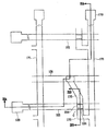
本発明の実施形態による薄膜トランジスタ表示板は、絶縁基板110上にゲート信号を伝達する複数のゲート線121及び蓄積電極線131が形成されている。
In the thin film transistor array panel according to the embodiment of the present invention, a plurality of
ゲート線121は、主に横方向に延びて互いに分離され、各ゲート線121の一部は複数のゲート電極124をなし、他の層または外部装置と接続するために広い面積の端部129を有する。
The
それぞれの蓄積電極線131は、主に横方向に延びてゲート線121と電気的に分離されている。蓄積電極線131は、蓄積電極をなす突出部を有することができ、蓄積電極線131には他の表示板の共通電極に印加される共通電圧など所定の電圧が印加される。
Each
ゲート線121及び蓄積電極線131は、Al、Al合金、Ag、Ag合金、Cr、Ti、Ta、Mo、Cuなどの金属、またはこれらを含む合金などで形成される。図2に示すように、本実施形態において、ゲート線121は物理的性質が異なる二つの膜、つまり、下部膜121pとその上の上部膜121qを有する。下部膜121pは、ゲート信号の遅延や電圧降下を減らすために、低い比抵抗の金属、例えば、アルミニウム(Al)やアルミニウム合金などのアルミニウム系金属からなり、1000〜300nm範囲の厚さを有する。これに対し、上部膜121qは、他の物質、特にIZO(indiumzinc oxide)またはITO(indium tin oxide)との物理的、化学的、電気的接触特性が優れた物質、例えば、モリブデン(Mo)、モリブデン合金(例:モリブデン-タングステン(MoW)合金)、クロム(Cr)などからなり、100〜100nm範囲の厚さを有する。下部膜121pと上部膜121qの組み合わせの例としては、純アルミニウムまたはアルミニウム-ネオジム(Nd)合金/モリブデンがあり、位置が互いに入れ替わることも可能である。図2で、ゲート電極124の下部膜と上部膜には各々図面符号124p、124q、ゲート線121端部129の下部膜と上部膜には各々図面符号129p、129q、蓄積電極線131の下部膜と上部膜には各々図面符号131p、131qを付けた。ゲート線121端部129の上部膜129qの一部は除去され、その下の下部膜129pの一部を露出させてもよい。
The
下部膜121p、124p、129p、131pと上部膜121q、124q、129q、131qの側面はそれぞれ傾斜しており、その側壁の傾斜角は基板110表面に対して約30〜80°である。
The side surfaces of the
ゲート線121と蓄積電極線131上には、窒化ケイ素(SiNx)などからなるゲート絶縁膜140が形成されている。
A
ゲート絶縁膜140上部には、水素化非晶質シリコン(非晶質シリコンはアモルファスシリコンとも呼ばれ、a-Siと略称する。)または多結晶シリコンなどからなる複数の線状半導体151が形成されている。各々の線状半導体151は、主に縦方向に延び、各々はゲート電極124に向けて延びた複数の突出部154を有する。
A plurality of
線状半導体151上部には、シリサイドまたはn型不純物が高濃度にドーピングされているn+水素化非晶質シリコンなどの物質で形成された複数の線状及び島状オーミック接触部材161、165が形成されている。線状オーミック接触部材161それぞれは複数の突出部163を有し、この突出部163と島状オーミック接触部材165は対をなして半導体151の突出部154上に配置されている。
A plurality of linear and island-shaped
線状半導体151とオーミック接触部材161、165の側面も基板110表面に対して傾斜しており、その傾斜角は30〜80°であることが好ましい。
The side surfaces of the
抵抗接触部材161、165上には、各々複数のデータ線171と複数のドレイン電極175が形成されている。
A plurality of
データ線171は、主に縦方向に延びてゲート線121及び蓄積電極線131と交差し、データ電圧を伝達し、他の層または外部装置と接続するために広い面積の端部179を有する。
The
それぞれのドレイン電極175は、蓄積電極線131上部まで延び蓄積電極線131の一部と重なる。
Each
また、各データ線171は、各ドレイン電極175に向けて複数の分枝を形成し、データ線171から拡張されたソース電極173を有する。一つのゲート電極124、一つのソース電極173、及び一つのドレイン電極175は、半導体151の突出部154と共に一つの薄膜トランジスタ(TFT)をなし、薄膜トランジスタのチャネル(channel)は、ソース電極173とドレイン電極175との間の突出部154に形成される。
Each
データ線171、ドレイン電極175もゲート線121と同様に、Al、Al合金、Ag、Ag合金、Cr、Ti、Ta、Mo、Cuなどの金属、またはこれらを含む合金などで形成され、単一膜または多層膜からなり、多層膜の例として、ゲート線121の上部膜と下部膜の組み合わせからなる2層膜、またはMoまたはMo合金/AlまたはAl合金/MoまたはMo合金からなる3層膜がある。
Similarly to the
このとき、半導体151は、薄膜トランジスタが位置するチャネル部154を除く、データ線171、ドレイン電極175及びその下部のオーミック接触部材161、165と実質的に同一の平面形状を有する。具体的には、線状半導体151は、データ線171及びドレイン電極175とその下部のオーミック接触部材161、165下に存在する部分以外にも、ソース電極173とドレイン電極175との間にこれらで覆われず露出する部分を有する。
At this time, the
データ線171及びドレイン電極175と、これらで覆われず露出する半導体151部分上には、平坦化特性が優れ、かつ感光性を有する有機物質、プラズマ化学気相蒸着(PECVD)で形成されるa-Si:C:O、a-Si:O:Fなどの低誘電率絶縁物質、または無機物質である窒化ケイ素や酸化ケイ素などからなる保護膜180が形成されている。本実施形態において、保護膜180は、下部に位置し半導体151のチャネル部が有機物と直接接触しないように保護し、窒化ケイ素または酸化ケイ素からなる下部絶縁膜180pと、平坦化特性を有し有機絶縁物質からなる上部絶縁膜180qの二重膜構造を有する。このとき、上部絶縁膜180qは、赤色、緑色及び青色などの原色のうちの一つを表示することができるカラーフィルタであってもよい。
On the
保護膜180には、ドレイン電極175の少なくとも一部とデータ線171の端部179をそれぞれ露出させる複数のコンタクトホール185q、182が備えられ、ゲート絶縁膜140と共にゲート線121の端部129を露出させる複数のコンタクトホール181が形成されている。ここで、ドレイン電極175の端部を露出させるコンタクトホール185pは、下部絶縁膜180pのみが有し、上部絶縁膜180qは、蓄積電極線131上部の大部分の下部絶縁膜180pを露出させる開口部185qを有する。開口部185q内には、ドレイン電極175の端部を露出させるコンタクトホール185pが位置し、ドレイン電極175の縦境界線は開口部185q内に位置する。このとき、ドレイン電極175下部に残留する非晶質シリコン層を最少化するために、ドレイン電極175が占める面積を最少化することが好ましく、特に、蓄積電極線131上部に位置するドレイン電極175端部の面積を最少化することが好ましい。
The
保護膜180上には、IZOまたはITOなどの透明な導電物質からなる複数の画素電極190及び複数の接触補助部材81、82が形成されている。
A plurality of
画素電極190は、コンタクトホール185pを介してドレイン電極175と物理的・電気的に接続されドレイン電極175からデータ電圧の印加を受ける。データ電圧が印加された画素電極190は、共通電圧の印加を受ける他の表示板(図示せず)の共通電極(図示せず)と共に電場を生成することによって液晶層の液晶分子を再配列する。
The
また、前述したように、画素電極190と共通電極は、キャパシタ(以下、“液晶キャパシタ”と言う。)をなして薄膜トランジスタがターンオフされた後にも印加された電圧を保持しており、電圧保持能力を強化するために、液晶キャパシタと並列に接続された他のキャパシタを設ける。これをストレージキャパシタと言う。ストレージキャパシタは、画素電極190とこれと隣接するゲート線121(これを前段ゲート線と言う。)または蓄積電極線131の重なりなどで形成される。
In addition, as described above, the
本発明において、画素電極190と蓄積電極線131は、上部絶縁膜180qの開口部185qによってゲート絶縁膜140及び下部絶縁膜180qのみを介在し重なってストレージキャパシタをなしているので、蓄積容量を安定的に確保でき、狭い面積でも十分な蓄積容量を形成することができる。その結果、蓄積容量による画面のフリッカー現象または残像を防止することができ、良好な表示特性を確保でき、高い開口率を得ることができる。
In the present invention, since the
本実施形態と異なって、別途の蓄積電極線131を配置せず、画素電極190と前段ゲート線121の重なりでストレージキャパシタを形成するときは、ゲート絶縁膜140を露出させる上部絶縁膜180qの開口部185qを前段ゲート線121上部に配置することもでき、その場合、画素電極190と重なる前段ゲート線121の一部を拡張することが好ましい。
Unlike the present embodiment, when the storage capacitor is formed by overlapping the
また、上部絶縁膜180qがカラーフィルタを有する実施形態では、ゲート線121及びデータ線171の端部129、179が位置するパッド領域にカラーフィルタが残留しない。
In the embodiment in which the upper insulating
また、画素電極190は、隣接するゲート線121及びデータ線171と重なって開口率を高めているが、重ならなくてもよい。
Further, although the
接触補助部材81、82は、コンタクトホール181、182を介してゲート線及びデータ線の端部129、179にそれぞれ接続される。接触補助部材81、82は、ゲート線121及びデータ線171の各終端部129、179と駆動集積回路のような外部装置との接着性を補完し、これらを保護する役割を果たすものであって、これらの適用は選択的である。
The
本発明の他の実施形態によれば、画素電極190の材料として透明な導電性ポリマーなどを使用し、反射型液晶表示装置の場合、不透明な反射性金属を使用しても良い。このとき、接触補助部材81、82は、画素電極190と異なる物質、特にIZOまたはITOで形成することができる。
According to another embodiment of the present invention, a transparent conductive polymer may be used as the material of the
以下、図1乃至図3に示す構造を有する液晶表示装置用薄膜トランジスタ表示板を本発明の一実施形態に従って製造する方法について、図4乃至図11B及び図1乃至図3を参照して詳細に説明する。 Hereinafter, a method of manufacturing a thin film transistor array panel for a liquid crystal display device having the structure shown in FIGS. 1 to 3 according to an embodiment of the present invention will be described in detail with reference to FIGS. 4 to 11B and FIGS. To do.
図4は、本発明の一実施形態に従って製造する第1工程の薄膜トランジスタ表示板の配置図であり、図5A及び図5Bは、各々図4のVa-Va線及びVb-Vb線に沿った断面図であり、図6A及び図6Bは、各々図4のVa-Va線及びVb-Vb線に沿った断面図であり、図5A及び図5Bに続く工程における断面図であり、図7A及び図7Bは、各々図4のVa-Va線及びVb-Vb線に沿った断面図であり、図6A及び図6Bに続く工程における断面図であり、図8は、図7A及び図7Bに続く工程における薄膜トランジスタ表示板の配置図であり、図9A及び図9Bは、各々図8のIXa-IXa線及びIXb-IXb線に沿った断面図であり、図10は、図9A及び図9Bに続く工程における薄膜トランジスタ表示板の配置図であり、図11A及び図11Bは、各々図10のXIa-XIa線及びXIb-XIb線に沿った断面図である。 4 is a layout view of a thin film transistor array panel of a first process manufactured according to an embodiment of the present invention. FIGS. 5A and 5B are cross-sectional views taken along lines Va-Va and Vb-Vb of FIG. 4, respectively. 6A and 6B are cross-sectional views taken along lines Va-Va and Vb-Vb in FIG. 4, respectively, and are cross-sectional views in the process subsequent to FIGS. 5A and 5B. 7B is a cross-sectional view taken along lines Va-Va and Vb-Vb in FIG. 4, respectively. FIG. 8B is a cross-sectional view in the process following FIGS. 6A and 6B, and FIG. 8 is a process following FIG. 7A and FIG. 9A and 9B are cross-sectional views taken along lines IXa-IXa and IXb-IXb in FIG. 8, respectively, and FIG. 10 is a process following FIG. 9A and FIG. 9B. In FIG. 11A and 11B are sectional views taken along XIa-XIa line and XIb-XIb line of each diagram 10.
まず、透明なガラスなどからなる絶縁基板110上に二層の金属膜、つまり、純アルミニウムまたはアルミニウム合金(Al-Nd alloy)の下部金属膜と、モリブデンまたはモリブデン合金の上部金属膜をスパッタリングなどで順次に積層する。ここで、下部金属膜は1000〜300nm程度の厚さを有することが好ましく、上部金属膜は500〜100nm程度の厚さを有することが好ましい。
First, a two-layer metal film, that is, a lower metal film of pure aluminum or an aluminum alloy (Al—Nd alloy) and an upper metal film of molybdenum or a molybdenum alloy are sputtered on an insulating
次に、図4、図5A及び図5Bに示すように、感光膜パターンを用いたフォトエッチング工程で上部金属膜と下部金属膜を順次にパターニングして、複数のゲート電極124を有するゲート線121と蓄積電極線131を形成する。
Next, as shown in FIGS. 4, 5 </ b> A, and 5 </ b> B, the upper metal film and the lower metal film are sequentially patterned by a photo-etching process using a photosensitive film pattern to form a
上部膜121q、131q及び下部膜121p、131pのパターニングは、アルミニウム及びモリブデンに対し全て側面傾斜を与えながらエッチングできるアルミニウムエッチング液であるCH3COOH(酢酸)/HNO3(硝酸)/H3PO4(リン酸)/H2Oを用いたウエットエッチングで行なうことが好ましい。
The patterning of the
次に、図6A及び図6Bに示すように、ゲート絶縁膜140、真性非晶質シリコン層150、不純物非晶質シリコン層160を化学気相蒸着法で各々約150nm乃至約500nm、約50nm乃至約200nm、約30nm乃至約60nmの厚さに連続蒸着する。次いで、スパッタリングなどの方法でデータ用導電物質を積層して導電体層170を形成した後、その上に感光膜を1μm乃至2μmの厚さに塗布する。その後、光マスクによって感光膜に光を照射した後、現像して感光膜パターン52、54を形成する。
Next, as shown in FIGS. 6A and 6B, the
このように現象された感光膜の厚さは位置によって異なり、感光膜は厚さが次第に薄くなる第1乃至第3部分からなる。A領域に位置した第1部分と、C領域に位置した第2部分は、各々図面符号52と54を付け、B領域に位置した第3部分に対する図面符号は付けない。これは第3部分が0の厚さを有しており、下の導電体層170が露出しているためである。第1部分52と第2部分54の厚さの比は後続工程の工程条件によって異なるようにし、第2部分54の厚さを第1部分52の厚さの1/2以下とすることが好ましく、例えば、400nm以下であることが好適である。ここで、A領域はデータ線171及びドレイン電極175に対応する配線領域に対応し、C領域はソース電極173とドレイン電極175との間のチャネル領域に対応し、B領域はA領域とC領域を除くその他の領域に対応する。
The thickness of the photosensitive film thus caused varies depending on the position, and the photosensitive film is composed of first to third portions whose thickness is gradually reduced. The first part located in the A area and the second part located in the C area are respectively attached with the
このとき、一つのマスクを用いたフォト工程で位置によって感光膜の厚さを異なるようにする方法は様々であり、第2部分54に対応する部分の光透過量を調節するために、主にスリットや格子形態のパターンを形成したり、半透過膜を用いる。
At this time, there are various methods for changing the thickness of the photosensitive film depending on the position in the photo process using one mask, and mainly for adjusting the light transmission amount of the portion corresponding to the
ここで、スリット間に位置したパターンの線幅やパターン間の間隔、つまり、スリットの幅は露光時使用する露光器の分解能より小さいことが好ましく、半透過膜を使用する場合には、マスクの製作時に透過率を調節するために、異なる透過率を有する薄膜を利用したり、異なる厚さを有する薄膜を使用することができる。 Here, the line width of the pattern located between the slits and the interval between the patterns, that is, the width of the slit is preferably smaller than the resolution of the exposure device used at the time of exposure. To adjust the transmittance during fabrication, thin films having different transmittances or thin films having different thicknesses can be used.
その後、感光膜パターン52、54をエッチングマスクとして用いた一連のエッチング工程により、図8、図9A及び図9Bに示すように、複数のソース電極173をそれぞれ有する複数のデータ線171及び複数のドレイン電極175を形成し、複数の突出部163をそれぞれ有する複数の線状オーミック接触部材161及び複数の島状オーミック接触部材165、並びに複数のチャネル部154を有する複数の線状半導体151を形成する。
Thereafter, through a series of etching steps using the
説明上、A領域に位置した導電体層170、不純物非晶質シリコン層160、真性非晶質シリコン層150の部分を第1部分とし、C領域に位置した導電体層170、不純物非晶質シリコン層160、真性非晶質シリコン層150の部分を第2部分とし、B領域に位置した導電体層170、不純物非晶質シリコン層160、真性非晶質シリコン層150の部分を第3部分とする。
For the sake of explanation, the
次に、このような構造を形成する順序の一例を示す。
(1)B領域に位置した導電体層170、不純物非晶質シリコン層160及び非晶質シリコン層150の第3部分除去、
(2)C領域に位置した感光膜の第2部分54除去、
(3)C領域に位置した導電体層170及び不純物非晶質シリコン層160の第2部分除去、
(4)A領域に位置した感光膜の第1部分52除去。
次に、このような順序の他の例を示す。
(1)B領域に位置した導電体層170の第3部分除去、
(2)C領域に位置した感光膜の第2部分54除去、
(3)B領域に位置した不純物非晶質シリコン層160及び非晶質シリコン層150の第3部分除去、
(4)C領域に位置した導電体層170の第2部分除去、
(5)A領域に位置した感光膜の第1部分52除去、
(6)C領域に位置した不純物非晶質シリコン層160の第2部分除去。
Next, an example of the order of forming such a structure is shown.
(1) Removal of the third portion of the
(2) removing the
(3) removing the second portion of the
(4) Removal of the
Next, another example of such an order is shown.
(1) removing the third portion of the
(2) removing the
(3) removing a third portion of the impurity
(4) removing the second portion of the
(5) removal of the
(6) The second partial removal of the impurity
ここでは、前記第2例について説明する。 Here, the second example will be described.
まず、図7A及び図7Bに示すように、B領域に露出している導電体層170をウエットまたは乾式エッチングで除去し、下部の不純物非晶質シリコン層160の第3部分を露出させる。アルミニウム系導電膜は主にウエットエッチングを施し、モリブデン系導電膜はウエット及び乾式エッチングを選択的に施すことができ、多重膜の場合には、ウエット及び乾式エッチングを選択的に施すことができる。また、二重膜がアルミニウムとモリブデンを含む場合には、一つのウエットエッチング条件でパターニングしてもよい。乾式エッチングを行なう場合、感光膜52、54上の部分の厚さがある程度エッチングされることができる。
First, as shown in FIGS. 7A and 7B, the
次に、B領域に位置した不純物非晶質シリコン層160及びその下部の真性非晶質シリコン層150の第3部分を除去すると共に、C領域の感光膜第2部分54を除去して下の導電体174の第2部分を露出させる。感光膜の第2部分54の除去は、不純物非晶質シリコン層160及び真性非晶質シリコン層150の第3部分の除去と同時にまたは個別に行う。このとき、C領域に残っている第2部分54の残渣をアッシング(ashing)処理で除去する。
Next, the impurity
この段階で線状真性半導体151が完成する。なお、図面符号164は線状オーミック接触部材161と島状オーミック接触部材165がまだ連結している状態の不純物非晶質シリコン層160を指し、以下、不純物半導体と言う。
At this stage, the linear
図面符号174は、データ線171とドレイン電極175がまだ連結している状態の導電体である。このとき、導電体174は、感光膜52、54の下部までエッチングされて導電体174及び感光膜52、54はアンダーカット構造を有する。
次に、図8、図9A及び図9Bに示すように、C領域に位置した残りの導電体174及び不純物半導体164の第2部分をエッチングして除去する。また、残っている感光膜の第1部分52も除去する。
Next, as shown in FIGS. 8, 9A, and 9B, the remaining portions of the
このとき、図9Bに示すように、C領域に位置した線状真性半導体151のチャネル部154上の部分が除去されて厚さが薄くなることもあり、感光膜の第1部分52もこのときある程度の厚さがエッチングされる。
At this time, as shown in FIG. 9B, the portion of the linear
このようにすれば、導電体174それぞれが一つのデータ線171及び複数のドレイン電極175に分離されて完成し、不純物半導体164それぞれが一つの線状オーミック接触部材161と複数の島状オーミック接触部材165に分離されて完成する。
In this way, each
次に、図10、図11A及び図11Bに示すように、基板110上部に窒化ケイ素と有機絶縁物質を順次に形成して下部絶縁膜180pと上部絶縁膜180qを有する保護膜180を形成した後、マスクを用いたフォトエッチング工程でパターニングして複数のコンタクトホール185p、182及び複数の開口部185qを形成する。このとき、ゲート線121と同一層を露出させるコンタクトホールを形成するために、ゲート絶縁膜140も同時にエッチングして、ゲート線121の端部129を露出させるコンタクトホール181を共に形成する。この際にも、位置によって厚さを異なるようにする感光膜パターンをエッチングマスクとして、互いに異なる形状を有する下部絶縁膜180pと上部絶縁膜180qを一つのフォトエッチング工程でパターニングすることができ、上部絶縁膜180qがカラーフィルタを有する実施形態ではカラーフィルタを別途のフォト工程で形成し、このとき、蓄積電極線131上部の下部絶縁膜180pを露出させる開口部185qを共に形成する。
Next, as shown in FIGS. 10, 11A, and 11B, silicon nitride and an organic insulating material are sequentially formed on the
最後に、図1乃至図3に示すように、50nm乃至150nm厚さのIZOまたはITO層をスパッタリング法で蒸着しフォトエッチングして、複数の画素電極190及び複数の接触補助部材81、82を形成する。IZO層を用いる場合のエッチングは、(HNO3/(NH4)2Ce(NO3)6/H2O)などのクロム用エッチング液を使用するウエットエッチングであることが好ましく、このエッチング液はアルミニウムを腐蝕させないので、データ線171、ドレイン電極175、ゲート線121の導電膜が腐食することを防ぐことができる。
Finally, as shown in FIGS. 1 to 3, an IZO or ITO layer having a thickness of 50 nm to 150 nm is deposited by sputtering and photoetched to form a plurality of
本実施形態において、データ線171及びドレイン電極175とその下部のオーミック接触部材161、165及び半導体151を一つの感光膜パターンをエッチングマスクとして用いるフォトエッチング工程で形成するので、製造工程を単純化することができる。
In this embodiment, the
また、本実施形態による薄膜トランジスタ表示板及びその製造方法において、蓄積電極線131上部に開口部185qを配置し、画素電極190と蓄積電極線131との間のゲート絶縁膜140及び下部絶縁膜180pのみを誘電体とするストレージキャパシタを形成する。従って、ドレイン電極175下部に残留する非晶質シリコンの面積を減少することによって、安定した蓄積容量を形成することができ、狭い面積でも十分な蓄積容量を形成することができる。その結果、蓄積容量による画面のフリッカー(flicker)現象または残像を防止することができ、良好な表示特性が実現され、高い開口率を得ることができる。
In the thin film transistor array panel and the method of manufacturing the same according to the present embodiment, an
一方、広視野角を実現するための手段として、電界生成電極は切開部を有したり、電界生成電極上に突起を形成する方法などがある。切開部と突起で液晶分子が傾斜する方向を決定できるので、液晶分子の傾斜方向を様々な方向に分散することによって広視野角を実現することができる。 On the other hand, as means for realizing a wide viewing angle, there are a method in which the electric field generating electrode has an incision portion or a protrusion is formed on the electric field generating electrode. Since the direction in which the liquid crystal molecules are tilted can be determined by the cut portion and the protrusion, a wide viewing angle can be realized by dispersing the tilt directions of the liquid crystal molecules in various directions.
図12は、本発明の他の実施形態による液晶表示装置用薄膜トランジスタ表示板の構造を示した配置図であり、図13は、本発明の一実施形態による液晶表示装置用共通電極表示板の構造を示した配置図であり、図14は、図12の薄膜トランジスタ表示板と、図13の共通電極表示板からなる液晶表示装置の構造を示した配置図であり、図15は、図14の液晶表示装置のXV-XV´線に沿った断面図である。 FIG. 12 is a layout view illustrating a structure of a thin film transistor array panel for a liquid crystal display according to another embodiment of the present invention, and FIG. 13 is a diagram illustrating a structure of a common electrode display panel for a liquid crystal display according to an embodiment of the present invention. FIG. 14 is a layout diagram showing the structure of a liquid crystal display device comprising the thin film transistor panel of FIG. 12 and the common electrode panel of FIG. 13, and FIG. 15 is a diagram of the liquid crystal of FIG. It is sectional drawing along the XV-XV 'line | wire of the display apparatus.
本発明の実施形態による液晶表示装置は、薄膜トランジスタ表示板100、共通電極表示板200、これら二つの表示板100、200の間に挿入されている液晶層3を備える。
The liquid crystal display according to an embodiment of the present invention includes a thin film
本実施形態による薄膜トランジスタ表示板100の層状構造は、図1乃至図3と略同様である。
The layered structure of the thin film
まず、薄膜トランジスタ表示板100は、ゲート電極124を有する複数のゲート線121及び複数の蓄積電極線131が基板110上に形成され、その上にゲート絶縁膜140、突出部154を有する線状半導体151、及び突出部163を有する複数の線状オーミック接触部材161及び複数の島状オーミック接触部材165が順次に形成されている。ソース電極173を有する複数のデータ線171及び複数のドレイン電極175がオーミック接触部材161、165及びゲート絶縁膜140上に形成され、下部絶縁膜180pがその上に形成され、下部絶縁膜180p及びゲート絶縁膜140には、複数のコンタクトホール181、182、185が形成されている。下部絶縁膜180p上には、複数の画素電極190及び複数の接触補助部材81、82が形成されている。
First, in the thin film
図1乃至図3と異なって、複数のゲート電極124は、ゲート線121で複数の突出部をなし、それぞれの蓄積電極線131は蓄積電極135をなす複数の突出部をそれぞれ有する。
Unlike FIG. 1 to FIG. 3, the plurality of
それぞれのドレイン電極175は、それぞれの蓄積電極135と重なる拡張部を有し、ドレイン電極175の拡張部は、蓄積電極135よりも小さい面積を有する。
Each
ソース電極173は、半導体151の突出部154上部に位置するドレイン電極175の一端部を一部取り囲むように折れ曲がっている。
The
また、下部絶縁膜180p上部には赤色、緑色及び青色などの原色のうちの一つを表示できるカラーフィルタ230を有する上部絶縁膜が形成され保護膜をなす。このとき、カラーフィルタ230は、蓄積電極135上部に位置する大部分の下部絶縁膜180pを露出させる開口部235を有する。カラーフィルタ230は、画素電極190に沿って縦方向に長く延び、データ線171を中心に互いに隣接する領域に位置するカラーフィルタ230は互いに異なる色を表示し、赤色、緑色及び青色を順次に表示することが好ましい。
Further, an upper insulating film having a
この際にも、前記実施形態と同様に、コンタクトホール185を介してドレイン電極175に接続されている画素電極190は、カラーフィルタ230の開口部235によってゲート絶縁膜140及び下部絶縁膜180pのみを介在して蓄積電極135と重なってストレージキャパシタをなす。
At this time, similarly to the above-described embodiment, the
画素電極190は、その外側境界の左角が面取りされた略四角形状で、中央切開部91、下部切開部92a及び上部切開部92bを有し、画素電極190は、この切開部91、92a、92bによって複数の領域に分割される。切開部91、92a、92bは、画素電極190をゲート線121と平行に二等分する横中心線に対し略反転対称をなす。
The
下部及び上部切開部92a、92bは、略画素電極190の右辺から左辺に斜めに延び、画素電極190の横中心線に対して下半面と上半面にそれぞれ位置している。下部及び上部切開部92a、92bはゲート線121に対して約45度をなし、互いに垂直に延びている。
The lower and
中央切開部91は、画素電極190の中央に配置され、右側に入口を有する。中央切開部91の入口は、下部切開部92aと上部切開部92bに各々略平行である一対の斜辺を有する。
The
これにより、画素電極190の下半面は下部切開部92aによって2領域に分割され、上半面も上部切開部92bによって2領域に分割される。このとき、領域の数または切開部の数は画素の大きさ、画素電極の横辺と縦辺の長さ比、液晶層3の種類や特性など設計要素によって変化し、傾斜する方向も変化することができる。
Accordingly, the lower half surface of the
次に、図13乃至図15を参照して、共通電極表示板200について説明する。
Next, the
透明なガラスなどからなる絶縁基板210上に遮光部材220が形成されている。遮光部材220は、画素電極190と対向し画素電極190と略同一の形状を有する複数の開口部を有し、ゲート線121及びデータ線171に対応する部分と、薄膜トランジスタに対応する部分とからなることが好ましい。
A
遮光部材220上部にはカバー膜250が形成され、その上部にはITO、IZOなどの透明な導電体などからなる共通電極270が形成されている。このとき、カバー膜250は省略することができる。
A
共通電極270は、複数組の切開部71、72a、72b群を有する。
The
一組の切開部71、72a、72bは、一つの画素電極190と対向し、中央切開部71、下部切開部72a及び上部切開部72bを有する。切開部71、72a、72bそれぞれは画素電極190の隣接切開部91、92a、92bの間または切開部92a、92bと画素電極190の面取りされた斜辺の間に配置されている。また、各切開部71、72a、72bは、画素電極190の下部切開部92aまたは上部切開部92bと平行に延びた少なくとも一つの斜線部を有する。
The pair of
下部及び上部切開部72a、72bそれぞれは、略画素電極190の左辺から上辺または下辺に向けて延びた斜線部、並びに斜線部の各終端から画素電極190の辺に沿って辺と重なって延び、斜線部と鈍角をなす横部及び縦部を有する。
Each of the lower and
中央切開部71は、略画素電極の左辺から横方向に延びた中央横部、この中央横部の終端から中央横部と斜角をなし、画素電極190の右辺に向けて延びた一対の斜線部、並びに斜線部の各終端から画素電極の右辺に沿って右辺と重なって延び、斜線部と鈍角をなす縦断縦部を有する。
The
切開部71、72a、72bの数及び方向も設計要素によって変化することが可能であり、遮光部材220が切開部71、72a、72bと重なって切開部71、72a、72b付近の光漏れを遮断することができる。
The number and direction of the
表示板100、200の内側面には配向膜11、21が塗布され、垂直配向膜であることができる。外側面には偏光板12、22が備えられている。二つの偏光板の透過軸は直交し、このうちの一つの透過軸はゲート線121に対して平行であることが好ましい。反射型液晶表示装置の場合には、二つの偏光板12、22のうちの一つが省略可能である。
表示板100、200と偏光子12、22との間にはそれぞれ液晶層3の遅延値を補償するための位相遅延フィルムが介在されることができる。位相遅延フィルムは複屈折性を有し、液晶層3の複屈折性を逆に補償する役割を果たす。遅延フィルムとしては、一軸性または二軸性光学フィルムを使用し、特に、ネガティブの一軸性光学フィルムを使用することができる。
A phase retardation film for compensating the delay value of the
また、液晶表示装置は、偏光子12、22、位相遅延フィルム、表示板100、200及び液晶層3に光を供給する照明部を備えることができる。
In addition, the liquid crystal display device can include an illuminator that supplies light to the
液晶層3は、マイナスの誘電率異方性を有し、液晶層3の液晶分子310は電界がない状態でその長軸が二つの表示板の表面に対して垂直をなすように配向されている。従って、入射光は、直交偏光子12、22を通過できず遮断される。
The
共通電極270に共通電圧を印加し、画素電極190にデータ電圧を印加すると、表示板表面に略垂直である電界が生成される。液晶分子310は、電界に応答してその長軸が電界の方向に垂直をなすように方向を変えようとする。
When a common voltage is applied to the
一方、共通電極270及び画素電極190の切開部71、72a、72b、91、92a、92bと、これらと平行である画素電極190の斜辺は、電界を歪曲して液晶分子の傾斜方向を決定する水平成分を形成する。電界の水平成分は、切開部71、72a、72b、91、92a、92bの辺と画素電極190の斜辺に垂直である。一つの切開部群71、72a、72b、91、92a、92bは、画素電極190をそれぞれ二つの主辺を有する複数の副領域(sub-area)に分離し、各副領域の液晶分子の傾斜方向は、電界の水平成分によって定められる方向となり、傾斜方向は略4つの方向である。このように、液晶分子が様々な方向に傾斜するようにすると、液晶表示装置の基準視野角が大きくなる。
On the other hand, the cut-out
少なくとも一つの切開部91、92a、92b、71、72a、72bは、突起(図示せず)や陥没部(図示せず)に代えることができる。突起は、有機物または無機物で形成され、電界生成電極190、270の上または下に配置することができる。
At least one
一方、液晶分子310の傾斜方向と偏光子12、22の透過軸が45度をなすとき最高の輝度を得られるが、本実施形態では、全ドメインにおいて液晶分子310の傾斜方向がゲート線121と45°をなし、ゲート線121は、表示板100、200の周縁と垂直または水平である。その結果、本実施形態において、偏光子12、22の透過軸を表示板100、200の周縁に対して垂直または平行に付着すると最高の輝度を得られると同時に、偏光子12、22を安価に製造することができる。
On the other hand, the highest luminance can be obtained when the tilt direction of the liquid crystal molecules 310 and the transmission axes of the
切開部91、92a、92b、71、72a、72bの形状及び配置は変更することができる。
The shape and arrangement of the
前記実施形態で説明した薄膜トランジスタ表示板の多くの特徴は、図12乃至図15に示した薄膜トランジスタ表示板にも適用できる。 Many features of the thin film transistor array panel described in the above embodiment can be applied to the thin film transistor array panel shown in FIGS.
図16は、本発明の他の実施形態による薄膜トランジスタ表示板の配置図であり、図17は、本発明の他の実施形態による共通電極表示板の配置図であり、図18は、図16及び図17の二つの表示板を備える液晶表示装置の配置図であり、図19及び図20は、図18の液晶表示装置のXIXa-XIXa線及びXX-XXb線に沿った断面図である。 16 is a layout view of a thin film transistor array panel according to another embodiment of the present invention, FIG. 17 is a layout diagram of a common electrode panel according to another embodiment of the present invention, and FIG. FIG. 19 is a layout view of a liquid crystal display device including the two display panels of FIG. 17, and FIGS. 19 and 20 are cross-sectional views of the liquid crystal display device of FIG. 18 taken along lines XIXa-XIXa and XX-XXb.
本発明の他の実施形態による液晶表示装置も薄膜トランジスタ表示板100と、共通電極表示板200と、これら二つの表示板100、200の間に介在される液晶層3とを備える。
The liquid crystal display according to another embodiment of the present invention also includes a thin film
本実施形態による薄膜トランジスタ表示板100の層状構造は、図12乃至図15と略同様である。
The layered structure of the thin film
薄膜トランジスタ表示板100は、ゲート電極124を有する複数のゲート線121が基板110上に形成され、その上にゲート絶縁膜140、突出部154を有する線状半導体151、及び突出部163を有する複数の線状オーミック接触部材161及び複数の島状オーミック接触部材165が順次に形成されている。ソース電極173を有する複数のデータ線171及び複数のドレイン電極175がオーミック接触部材161、165及びゲート絶縁膜140上に形成され、保護膜180がその上に形成され、保護膜180及びゲート絶縁膜140には複数のコンタクトホール181、182、185が形成されている。保護膜180上には、複数の画素電極190及び複数の接触補助部材81、82が形成されている。
The thin film
前記実施形態と異なって別途の蓄積電極線を有しない。 Unlike the previous embodiment, no separate storage electrode line is provided.
線状半導体151と同一層からなり、隣接した二つのゲート線121の略中間部に位置する複数の島状半導体157が形成され、その上に島状オーミック接触部材167が形成されている。
A plurality of island-shaped
ソース電極173は、U字状で、一字状のドレイン電極175の一端を一部取り囲み、オーミック接触部材167上には、蓄積導電体177がデータ線171として形成されている。
The
保護膜180には、蓄積導電体177の一部を露出させる複数のコンタクトホール189が形成され、上部保護膜180qには、下部保護膜180pを露出させ、蓄積導電体177上部に位置する開口部187が形成されている。コンタクトホール181、182、185、189と開口部187は、緩慢な角度の側壁を有し、特に、上部保護膜180qからなるコンタクトホール181、182、185、189と開口部187側壁の上部は、基板110表面と約30〜85°をなしている。
The
画素電極190は、開口部187で蓄積導電体177と重なり、4つの角が面取りされて斜辺をなす。
The
画素電極190は、中央切開部91、92、下部切開部93a、94a、95a及び上部切開部93b、94b、95bを有し、画素電極190は、この切開部によって複数の領域に分割される。切開部91〜95bは、画素電極190を2等分する横中心線に対して略反転対称をなしている。
The
下部及び上部切開部93a〜95bは、略画素電極190の左辺、左角、下辺または上辺から右辺に斜めに延び、画素電極190横中心線に対して下半部と上半部にそれぞれ位置している。下部及び上部切開部93a〜95bは、ゲート線121に対して約45°をなし、互いに垂直に延びている。
The lower and
中央切開部91は、画素電極190の中央に配置され、左辺に位置した入口を有する。中央切開部91の入口は、下部切開部93a、94a、95aと上部切開部93b、94b、95bにそれぞれ略平行である一対の斜辺を有し、入口付近にコンタクトホール189が位置する。中央切開部92は、画素電極190の横中心線に沿って短く延びた横部と、横部から画素電極190の左側に向けて斜めに延びた一対の斜線部を有する。斜線部は、ゲート線121と略45°をなす。
The
切開部91〜95bによって分割される領域の数または切開部の数は、画素の大きさ、画素電極190の横辺と縦辺の長さ比、液晶層3の種類や特性などの設計要素によって変化し、傾斜方向も変化することが可能である。
The number of regions divided by the
遮蔽電極88は、データ線171に沿って延びている縦部と、ゲート線121に沿って延びている横部を有し、縦部はデータ線171を完全に覆い、横部はゲート線121の境界線の内側に位置する。遮蔽電極88の縦部は、コンタクトホール189を介して蓄積導電体177に接続される突出部89を有する。
The
遮蔽電極88は、共通電圧の印加を受け、データ線171と画素電極190との間及びデータ線171と共通電極270との間で形成される電界を遮断し、画素電極190の電圧歪曲及びデータ線171が伝達するデータ電圧の信号遅延が減少する。
The
また、画素電極190と遮蔽電極88の短絡を防止するために、これらの間に距離を設ける必要があるので、画素電極190がデータ線171から一層離れた所に配置され、これらの間の寄生容量が減少する。さらに、液晶層3の誘電率が保護膜180の誘電率よりも高いので、データ線171と遮蔽電極88との間の寄生容量は、遮蔽電極88がないときデータ線171と共通電極270との間の寄生容量よりも小さい。
Further, since it is necessary to provide a distance between the
遮蔽電極88から共通電圧の供給を受ける蓄積導電体177は、主に開口部187で下部保護膜180pのみを介在して画素電極190と重なることで、液晶キャパシタと並列に接続されて電圧保持能力を強化するストレージキャパシタをなす。
The
このように、無機絶縁物からなる下部保護膜180pのみを介在して画素電極190と蓄積導電体177が重なるので、ゲート線121と同一層に蓄積電極を別に設けなくても蓄積容量を確保できる。これにより、中間に介在される非晶質シリコンがないため、ストレージキャパシタが安定的に動作することができる。その結果、画面のフリッカー現象または残像を防止でき、良好な表示特性を実現できる。
As described above, since the
次に、共通電極表示板200について図17乃至図19を参照して説明する。
Next, the
共通電極表示板200は、前記実施形態と同様に、遮光部材220、カバー膜250、共通電極270及び配向膜21が絶縁基板210上に形成されている。
In the
遮光部材220は、データ線171に対応する線状部分221と薄膜トランジスタに対応する辺状部分223を有する。
The
また、基板210上には複数のカラーフィルタ230が形成され、画素電極190に沿って縦方向に長く延びている。カラーフィルタ230は、基本色、例えば、赤色、緑色及び青色の三原色のうちの一つを表示することができる。
In addition, a plurality of
カラーフィルタ230上には、カバー膜250が形成されている。カバー膜250は、カラーフィルタ23に含まれた色素が出て液晶層3を汚染することを防止し、平坦面を提供する。
A
共通電極270は、複数の切開部71、72、73a、74a、75a、73b、74b、75b群を有する。
The
一つの切開部71〜75b群は、一つの画素電極190と対向し、中央切開部71、72、下部切開部73a、74a、75a及び上部切開部73b、74b、75bを有する。切開部71〜75bそれぞれは、画素電極190の隣接切開部91〜95bの間または切開部93a〜95bと画素電極190の面取りされた斜辺の間に配置されている。また、各切開部71〜75bは、画素電極190の下部切開部93a、94a、95aまたは上部切開部93b、94b、95bと平行に延びた少なくとも一つの斜線部を有する。
One incision 71-75b group faces one
下部及び上部切開部74a、75a、74b、75bそれぞれは斜線部と横部及び縦部を有する。斜線部は、略画素電極190の上辺または下辺から右辺に延びている。横部及び縦部は、斜線部の各終端から画素電極190の辺に沿って重なって延び、斜線部と鈍角をなす。
Each of the lower and
下部及び上部切開部73a、73bそれぞれは、斜線部と一対の縦部を有する。斜線部は、略画素電極190の左辺から右辺に延びている。縦部は、斜線部の各終端から画素電極190の辺に沿って重なって延び、斜線部と鈍角をなす。
Each of the lower and
中央切開部71、72は、中央横部、一対の斜線部及び一対の縦断縦部を有する。中央横部は、画素電極190の右辺または中央から画素電極190の横中心線に沿って左に延び、斜線部は中央横部の終端から中央横部と斜角をなし、画素電極190の左辺に向けて延びている。縦断縦部は、斜線部の各終端から画素電極190の辺に沿って重なって延び、斜線部と鈍角をなす。
The
図21は、本発明の他の実施形態による液晶表示装置用薄膜トランジスタ表示板の配置図であり、図22は、本発明の他の実施形態による液晶表示装置用共通電極表示板の配置図であり、図23は、図21に示す薄膜トランジスタ表示板と、図22に示す共通電極表示板を備える液晶表示装置の配置図であり、図24は、図23の液晶表示装置のXXIV-XXIV´線に沿った断面図である。 FIG. 21 is a layout view of a thin film transistor array panel for a liquid crystal display according to another embodiment of the present invention, and FIG. 22 is a layout view of a common electrode display panel for a liquid crystal display according to another embodiment of the present invention. 23 is a layout view of the liquid crystal display device including the thin film transistor array panel shown in FIG. 21 and the common electrode display plate shown in FIG. 22. FIG. 24 is a cross-sectional view taken along line XXIV-XXIV ′ of the liquid crystal display device of FIG. FIG.
図21乃至図24に示すように、本実施形態による液晶表示装置も薄膜トランジスタ表示板100、共通電極表示板200、これら二つの表示板100、200の間に介在される液晶層3、及び二つの表示板100、200の外側面に付着されている一対の偏光子12、22を備える。
As shown in FIGS. 21 to 24, the liquid crystal display according to the present embodiment also includes a thin film
本実施形態による表示板100、200の層状構造は、図12乃至図15に示した表示板100、200の層状構造と略同様である。
The layered structure of the
薄膜トランジスタ表示板100は、ゲート電極124を有する複数のゲート線121が基板110上に形成され、その上にゲート絶縁膜140上に突出部154を有する複数の線状半導体151及び突出部163を有する複数の線状オーミック接触部材161及び島状オーミック接触部材165が順次に形成されている。ソース電極173を有する複数のデータ線171と複数のドレイン電極175がオーミック接触部材161、165及びゲート絶縁膜140上に形成され、下部絶縁膜180p及びカラーフィルタ230が順次に形成されて保護膜をなし、下部絶縁膜180p及びゲート絶縁膜140には、複数のコンタクトホール181、182、185が形成されている。カラーフィルタ230は、下部絶縁膜180p及びコンタクトホール185を露出させる開口部235を有し、保護膜180p、230上には、複数の画素電極190及び複数の接触補助部材81、82が形成され、その上に配向膜11が形成されている。
In the thin film
共通電極表示板200は、遮光部材220、カバー膜250、共通電極270及び配向膜21が絶縁基板210上に形成されている。
In the
しかし、図12乃至図15と異なって、ドレイン電極175は、画素電極190の中央部まで延びて横方向に拡張された拡張部を有し、カラーフィルタ230の開口部235は、ドレイン電極175の拡張部を露出させる。開口部235は、画素電極190とドレイン電極175を接続するコンタクトホール185まで延びているが、そうでないことも可能である。
However, unlike FIG. 12 to FIG. 15, the
画素電極190の4つの角が面取りされて斜辺をなし、これらと同一層には遮蔽電極88が形成されている。
Four corners of the
また、遮蔽電極88は、横方向に延びて画素電極190の凹部に位置し、カラーフィルタ230の開口部235によってドレイン電極175と重なる蓄積電極部85を有する。画素電圧が伝達されるドレイン電極175と共通電圧が伝達される蓄積電極部85は、互いに重なってストレージキャパシタをなす。このように、遮蔽電極88を拡張しドレイン電極175と重ならせてストレージキャパシタを形成することで、本実施形態では、前記実施形態のような別途の蓄積電極線が不要である。このとき、下部絶縁膜180pのみを介在しドレイン電極175と蓄積電極部85が重なることによって狭い面積で蓄積容量を十分確保できるので、不透明なドレイン電極175の面積を最少化することができ、その結果、画素の開口率を極大化することができる。このとき、遮蔽電極88の蓄積電極部85、カラーフィルタ230の開口部、及びドレイン電極175の拡張部は、液晶表示装置の表示特性を向上するために様々な形態に変形可能である。
The
前記実施形態で説明した液晶表示装置の多くの特徴は、図21乃至図24に示した液晶表示装置にも適用できる。 Many features of the liquid crystal display device described in the above embodiment can be applied to the liquid crystal display device shown in FIGS.
図25は、本発明の他の実施形態による液晶表示装置用薄膜トランジスタ表示板の構造を示した配置図であり、図26は、本発明の他の実施形態による液晶表示装置用共通電極表示板の構造を示した配置図であり、図27は、図25の薄膜トランジスタ表示板と、図26の薄膜トランジスタ表示板からなる液晶表示装置の構造を示した配置図であり、図28及び図29は、図26に示す液晶表示装置のXXVIII-XXVIII´線及びXXIX-XXIX´線に沿った断面図であり、図30は、本発明の実施形態による液晶表示装置の一つの画素の構成を示した回路図である。 FIG. 25 is a layout view illustrating a structure of a thin film transistor array panel for a liquid crystal display according to another embodiment of the present invention, and FIG. 26 illustrates a common electrode display panel for a liquid crystal display according to another embodiment of the present invention. FIG. 27 is a layout diagram showing the structure of a liquid crystal display device comprising the thin film transistor array panel of FIG. 25 and the thin film transistor panel of FIG. 26. FIGS. FIG. 30 is a cross-sectional view taken along line XXVIII-XXVIII ′ and line XXIX-XXIX ′ of the liquid crystal display device shown in FIG. 26, and FIG. 30 is a circuit diagram showing a configuration of one pixel of the liquid crystal display device according to the embodiment of the present invention. It is.
本実施形態による液晶表示装置も、薄膜トランジスタ表示板100、これと対向する共通電極表示板200、これら二つの表示板100、200の間に介在される液晶層3を備える。
The liquid crystal display device according to the present embodiment also includes a thin film
本実施形態による表示板100、200の層状構造は、図21乃至図24と略同様である。
The layered structure of the
薄膜トランジスタ表示板100は、ゲート電極124を有する複数のゲート線121が基板110上に形成され、その上にゲート絶縁膜140、突出部154を有する複数の線状半導体151及び突出部163を有する複数の線状オーミック接触部材161及び島状オーミック接触部材165が順次に形成されている。ソース電極173を有する複数のデータ線171と複数のドレイン電極175がオーミック接触部材161、165及びゲート絶縁膜140上に形成され、下部絶縁膜180p及びカラーフィルタ230が順次に形成され、下部絶縁膜180p及びゲート絶縁膜140には、複数のコンタクトホール181、182が形成されている。保護膜180p、230上には、複数の第1、第2画素電極190a、190b、及び複数の接触補助部材81、82が形成され、その上には配向膜11が形成されている。
In the thin film
共通電極表示板200は、遮光部材220、カバー膜250、共通電極270及び配向膜21が絶縁基板210上に形成されている。
In the
図21乃至図24の液晶表示装置と異なって、ゲート線121と同一層に複数の蓄積電極線131a、131bが形成されている。
Unlike the liquid crystal display device of FIGS. 21 to 24, a plurality of
それぞれの蓄積電極線131a、131bは主に横方向に延び、互いに隣接するゲート線121の間にそれぞれ対をなして配置されている。それぞれの蓄積電極線131a、131bは、互いに隣接するゲート線121付近に位置し、蓄積電極135a、135bをなす複数の突出部をそれぞれ有する。二つの蓄積電極135a、135bは、他の部分よりも広い幅に拡張され、二つの蓄積電極線131a、131bは、ゲート線121と平行である第1、第2画素電極190a、190bの中心線に対して対称構造を有する。
The
それぞれのドレイン電極175は、それぞれの蓄積電極135a、135bとそれぞれ重なる長方形の拡張部175a、175bを有する。ドレイン電極175のそれぞれの拡張部175a、175bは、蓄積電極135a、135bよりも小さい面積を有していて、拡張部175a、175bで覆われない蓄積電極135a、135bの面積を極大化することが好ましく、ゲート線121と平行である第1、第2画素電極190a、190bの中心線に対して対称構造を有することが好ましい。
Each
また、ドレイン電極175は、ゲート線121とデータ線171で取り囲まれた領域の中央に位置する容量性結合電極176を有する。
The
また、ドレイン電極175は、二つの拡張部175a、175bと容量性結合電極176を互いにそれぞれ接続する連結部177a、177bを有する。
The
下部絶縁膜180には、一対のドレイン電極175の拡張部175a、175bをそれぞれ露出させる複数のコンタクトホール185a、185bが形成されている。
In the lower insulating
上部絶縁膜であるカラーフィルタ230には、対をなす蓄積電極135a、135b及びコンタクトホール185a、185bが位置するドレイン電極の拡張部175a、175b上部の下部絶縁膜180pをそれぞれ露出させる対をなす開口部235a、235bと容量性結合電極176上部の下部絶縁膜180pを露出させる開口部236が形成されている。
The
ここで、第1、第2画素電極190a、190bは、切開部93a、93bからなるギャップによって互いに分離されているが、第1画素電極190aは、コンタクトホール185a、185bを介してドレイン電極175の拡張部175a、175bと物理的・電気的に接続されドレイン電極175からデータ電圧の印加を受ける。第2画素電極190bは、ドレイン電極175の容量性結合電極176と重なる。これにより、第2画素電極190bは、第1画素電極190aに電磁気的に結合(容量性)して間接的にデータ電圧の印加を受ける。このとき、容量性結合電極176は、下部絶縁膜180pのみを介在しカラーフィルタ230の開口部236によって第2画素電極190bと重なっているので、狭い面積で充分な結合容量を確保でき、その結果、開口率を向上することができる。また、ドレイン電極175よりも広いカラーフィルタ230の開口部235a、235bによって第1画素電極190aと蓄積電極135a、135bが下部絶縁膜180pとゲート絶縁膜140のみを介在して重なっているので、狭い面積で充分な蓄積容量を形成でき、開口率の低下を防止することができる。
Here, the first and
一対の第1、第2画素電極190a、190bは、データ線171とゲート線121で取り囲まれた領域内に殆ど存在し、境界の大部分はゲート線121及びデータ線171と平行で長方形をなす。
The pair of first and
このとき、第1画素電極190aは、互いに分離され第2画素電極190bを中心に上部及び下部に位置する2部分からなる。第1画素電極190aの2部分と第2画素電極190bを分離するギャップ93a、93bは、ゲート線121に対して±45°傾斜された辺を有しており、第2画素電極190bが第1画素電極190aの2部分の間に介在した形態であり、第1、第2画素電極190a、190bは、ゲート線121と平行である第1、第2画素電極190a、190bの中心線に対して対称構造を有する。
At this time, the
このような本発明の実施形態による液晶表示装置は、前述したように、第2画素電極190bは、第1画素電極190aに電磁気的に結合(容量性結合)している。図30に示すように、第1画素電極190aの二部分は、ドレイン電極175を介して薄膜トランジスタQに直接接続されて薄膜トランジスタQを介してデータ線171によって伝達される画像信号電圧の印加を受けるのに対し、第2画素電極190bの電圧は、第1画素電極190aとの容量性結合に変わる。本実施形態において、第2画素電極190bの電圧は、第1画素電極190aの電圧よりも絶対値が常に低い。以下、その理由を具体的に説明する。
In the liquid crystal display device according to the embodiment of the present invention, as described above, the
図30で、Clcaは第1画素電極190aと共通電極270との間で形成される液晶容量を示し、Cstaは第1画素電極190aと蓄積電極線131との間で形成される蓄積容量を示す。Clcbは第2画素電極190bと共通電極270との間で形成される液晶容量を示し、Cstbは第2画素電極190bと蓄積電極線131との間で形成される蓄積容量を示し、Ccpは第2画素電極190bと第1画素電極190aとの間で形成される結合容量を示す。
In FIG. 30, Clca indicates a liquid crystal capacitance formed between the
共通電極270電圧に対する第1画素電極190aの電圧をVaとし、第2画素電極190bの電圧をVbとするとき、電圧法則に従って、
Vb=Va×[Ccp/(Ccp+Clcb+Cstb)]であり、
Ccp/(Ccp+Clcb+Cstb)は、常に1より大きくなることができず、VbはVaよりも常に小さい。このとき、Clca及びClcbに対する共通電極270電圧と、Csta及びCstbに対する蓄積電極線131a、131b電圧が異なることもあるが、その場合にも、ClcaとClcbに印加される共通電極270電圧が同一であるため、Clcaに印加される画像信号電圧(Va)の絶対値は、Clcbに印加される画像信号電圧(Vb)の絶対値よりも常に大きい値を有することになる。このように、一つの画素内に電圧が異なる二つの画素電極を配置すると、液晶分子は、互いに異なる電圧で駆動されて互いに異なる傾斜角(tilt angle)で傾斜され、その結果、側面視認性を向上することができる。
When the voltage of the
Vb = Va × [Ccp / (Ccp + Clcb + Cstb)],
Ccp / (Ccp + Clcb + Cstb) cannot always be greater than 1 and Vb is always less than Va. At this time, the
Ccpを調節することでVaに対するVbの比率を調整することができる。Ccpの調節は、容量性結合電極176と第2画素電極190bの重なり面積と距離を調整することによって可能である。重なり面積は、容量性結合電極176の幅を変化することで容易に調整でき、距離は、容量性結合電極176の形成位置を変化することで調整できる。即ち、本発明の実施形態では、容量性結合電極176をデータ線171と同一層に形成したが、ゲート線121と同一層に形成することで、容量性結合電極176と第2画素電極190bとの間の距離を増加することができる。このとき、VbはVaに対して0.6乃至0.8倍であることが好ましい。
The ratio of Vb to Va can be adjusted by adjusting Ccp. Ccp can be adjusted by adjusting the overlapping area and distance between the
一方、他の実施形態において、第2画素電極190bに第1画素電極190aの電圧よりも絶対値が常に高い電圧を印加することができるが、これは、第2画素電極190bに共通電圧などのように任意電圧を印加した状態で第1画素電極190aと容量性結合することによって行われる。
On the other hand, in other embodiments, a voltage whose absolute value is always higher than the voltage of the
画像信号が直接伝達される第1画素電極190aに対する、高いか、低い画素電圧が伝達される第2画素電極190bの面積比は1:0.85〜1:1.15範囲であることが好ましく、第1画素電極190aと容量性結合する第2画素電極190bは、二つ以上を配置することができる。
The area ratio of the
以上、本発明の好適な実施形態について詳細に説明したが、本発明の権利範囲はこれに限定されず、請求の範囲で定義している本発明の基本概念を利用した当業者の多様な変形及び改良形態も本発明の権利範囲に属するものである。 The preferred embodiment of the present invention has been described in detail above, but the scope of the present invention is not limited to this, and various modifications of those skilled in the art using the basic concept of the present invention defined in the claims. In addition, improvements are also within the scope of the present invention.
本発明は、薄膜トランジスタ表示板の製造に用いることができる。 The present invention can be used for manufacturing a thin film transistor array panel.
110 基板
121、129 ゲート線
124 ゲート電極
140 ゲート絶縁膜
151、154 半導体
161、163、165 オーミック接触部材
171、179 データ線
173 ソース電極
175 ドレイン電極
180 保護膜
181、182、185、185a、185b コンタクトホール
190、190a、190b 画素電極
81、82 接触補助部材
88 遮蔽電極
85 蓄積電極部
270 共通電極
220 遮光部材
230 カラーフィルタ
235、236 開口部
110
Claims (17)
前記ゲート線と交差するデータ線と、
前記ゲート線及び前記データ線と分離されている蓄積電極と、
前記ゲート線及び前記データ線に接続され、前記蓄積電極の上方に形成されるオーミック接触部材と半導体とドレイン電極を備える薄膜トランジスタと、
前記蓄積電極と前記ゲート線とを覆うゲート絶縁膜と、
前記ドレイン電極に接続されている画素電極と、
前記薄膜トランジスタを覆い、前記画素電極下部に配置され、前記ドレイン電極と前記画素電極とが接続するためのコンタクトホールが形成される第1絶縁膜と、
前記第1絶縁膜の上部に形成される第2絶縁膜とを備える薄膜トランジスタ表示板であって、
前記第2絶縁膜に前記蓄積電極に対応する部分で前記第1絶縁膜を露出させる開口部を形成することにより、前記蓄積電極と前記ゲート絶縁膜と前記第1絶縁膜と前記画素電極とから構成される蓄積容量が形成されることを特徴とする薄膜トランジスタ表示板。 A gate line,
A data line intersecting the gate line;
A storage electrode separated from the gate line and the data line;
A thin film transistor including an ohmic contact member, a semiconductor, and a drain electrode connected to the gate line and the data line and formed above the storage electrode;
A gate insulating film covering the storage electrode and the gate line;
A pixel electrode connected to the drain electrode;
A first insulating film that covers the thin film transistor, is disposed under the pixel electrode, and has a contact hole for connecting the drain electrode and the pixel electrode;
A thin film transistor array panel comprising: a second insulating film formed on the first insulating film;
By forming an opening in the second insulating film to expose the first insulating film at a portion corresponding to the storage electrode, the storage electrode, the gate insulating film, the first insulating film, and the pixel electrode are formed. A thin film transistor array panel, wherein a storage capacitor is formed.
Applications Claiming Priority (4)
| Application Number | Priority Date | Filing Date | Title |
|---|---|---|---|
| KR10-2005-0015914 | 2005-02-25 | ||
| KR1020050015914A KR101251993B1 (en) | 2005-02-25 | 2005-02-25 | Thin film transistor array panel |
| KR1020050034964A KR101143000B1 (en) | 2005-04-27 | 2005-04-27 | Thin film transistor array panel and manufacturing method thereof |
| KR10-2005-0034964 | 2005-04-27 |
Related Child Applications (1)
| Application Number | Title | Priority Date | Filing Date |
|---|---|---|---|
| JP2011285112A Division JP5703208B2 (en) | 2005-02-25 | 2011-12-27 | Thin film transistor array panel and manufacturing method thereof |
Publications (2)
| Publication Number | Publication Date |
|---|---|
| JP2006235635A JP2006235635A (en) | 2006-09-07 |
| JP5307319B2 true JP5307319B2 (en) | 2013-10-02 |
Family
ID=36931644
Family Applications (2)
| Application Number | Title | Priority Date | Filing Date |
|---|---|---|---|
| JP2006047707A Active JP5307319B2 (en) | 2005-02-25 | 2006-02-24 | Thin film transistor array panel and manufacturing method thereof |
| JP2011285112A Active JP5703208B2 (en) | 2005-02-25 | 2011-12-27 | Thin film transistor array panel and manufacturing method thereof |
Family Applications After (1)
| Application Number | Title | Priority Date | Filing Date |
|---|---|---|---|
| JP2011285112A Active JP5703208B2 (en) | 2005-02-25 | 2011-12-27 | Thin film transistor array panel and manufacturing method thereof |
Country Status (4)
| Country | Link |
|---|---|
| US (2) | US8305507B2 (en) |
| JP (2) | JP5307319B2 (en) |
| CN (2) | CN103034004A (en) |
| TW (1) | TWI423444B (en) |
Families Citing this family (19)
| Publication number | Priority date | Publication date | Assignee | Title |
|---|---|---|---|---|
| KR100831235B1 (en) * | 2002-06-07 | 2008-05-22 | 삼성전자주식회사 | A thin film transistor array panel |
| US8305507B2 (en) * | 2005-02-25 | 2012-11-06 | Samsung Display Co., Ltd. | Thin film transistor array panel having improved storage capacitance and manufacturing method thereof |
| TWI327239B (en) * | 2006-01-20 | 2010-07-11 | Au Optronics Corp | Pixel and liquid crystal display and method for manufacturing the same |
| KR20080001181A (en) * | 2006-06-29 | 2008-01-03 | 엘지.필립스 엘시디 주식회사 | An array substrate for lcd and method for fabricating thereof |
| JP5213587B2 (en) * | 2008-08-26 | 2013-06-19 | 株式会社ジャパンディスプレイウェスト | Liquid crystal display |
| US8471973B2 (en) * | 2009-06-12 | 2013-06-25 | Au Optronics Corporation | Pixel designs of improving the aperture ratio in an LCD |
| KR101765545B1 (en) * | 2010-07-07 | 2017-08-08 | 삼성디스플레이 주식회사 | Display apparatus |
| KR101778009B1 (en) * | 2010-08-19 | 2017-09-27 | 삼성디스플레이 주식회사 | Display panel and fabricating method thereof |
| KR101909139B1 (en) * | 2011-02-07 | 2018-12-19 | 삼성디스플레이 주식회사 | Thin film transistor array panel and manufacturing method thereof |
| CN102998859B (en) * | 2012-12-14 | 2016-03-02 | 京东方科技集团股份有限公司 | A kind of array base palte and preparation method thereof and display device |
| TW201427893A (en) | 2013-01-07 | 2014-07-16 | 群康科技(深圳)有限公司 | Patterned color conversion film and display using the same |
| CN103197480B (en) * | 2013-03-22 | 2015-07-01 | 京东方科技集团股份有限公司 | Array substrate and manufacture method thereof and display panel with same |
| TWI511303B (en) * | 2013-08-30 | 2015-12-01 | Ye Xin Technology Consulting Co Ltd | Array substrate of liquid crystal display |
| KR20150047399A (en) * | 2013-10-24 | 2015-05-04 | 삼성디스플레이 주식회사 | Liquid crystal display panel |
| KR102140815B1 (en) | 2013-12-09 | 2020-08-04 | 삼성디스플레이 주식회사 | Liquid crystal display |
| KR102132445B1 (en) * | 2013-12-31 | 2020-07-09 | 엘지디스플레이 주식회사 | Liquid Crystal Display Panel And Manufacturing Method Of The Same |
| CN105097552A (en) | 2015-08-14 | 2015-11-25 | 京东方科技集团股份有限公司 | Manufacturing methods of thin film transistor and array substrate, array substrate and display device |
| JP2019066719A (en) * | 2017-10-03 | 2019-04-25 | シャープ株式会社 | Display panel |
| CN114460782B (en) * | 2020-10-30 | 2023-10-20 | 京东方科技集团股份有限公司 | Array substrate, preparation method thereof and display device |
Family Cites Families (59)
| Publication number | Priority date | Publication date | Assignee | Title |
|---|---|---|---|---|
| JP3733344B2 (en) * | 1991-11-29 | 2006-01-11 | セイコーエプソン株式会社 | Liquid crystal display |
| JPH06347826A (en) | 1993-06-07 | 1994-12-22 | Sanyo Electric Co Ltd | Liquid crystal display device |
| JP3109967B2 (en) * | 1993-12-28 | 2000-11-20 | キヤノン株式会社 | Active matrix substrate manufacturing method |
| JPH10325961A (en) | 1994-03-17 | 1998-12-08 | Hitachi Ltd | Active matrix type liquid crystal display device |
| JPH0862629A (en) | 1994-08-16 | 1996-03-08 | Toshiba Corp | Liquid crystal display device |
| JPH0926603A (en) * | 1995-05-08 | 1997-01-28 | Semiconductor Energy Lab Co Ltd | Display device |
| JPH1010581A (en) * | 1996-06-25 | 1998-01-16 | Semiconductor Energy Lab Co Ltd | Display device |
| JPH1048664A (en) | 1996-07-19 | 1998-02-20 | Lg Electron Inc | Liquid crystal display device and its production |
| KR100207491B1 (en) | 1996-08-21 | 1999-07-15 | 윤종용 | Liquid crystal display device and its manufacturing method |
| JPH1073840A (en) | 1996-08-30 | 1998-03-17 | Toshiba Corp | Active matrix substrate, liquid crystal display element and its production |
| US6038006A (en) * | 1996-09-02 | 2000-03-14 | Casio Computer Co., Ltd. | Liquid crystal display device with light shield and color filter overlapping two edges of pixel electrode |
| KR100209623B1 (en) | 1996-09-13 | 1999-07-15 | 구자홍 | Liquid crystal display device and its manufacturing method |
| JPH1096949A (en) | 1996-09-24 | 1998-04-14 | Toshiba Electron Eng Corp | Active matrix liquid crystal display device |
| CN1148600C (en) | 1996-11-26 | 2004-05-05 | 三星电子株式会社 | Liquid crystal display using organic insulating material and manufacturing methods thereof |
| JP3264364B2 (en) | 1997-01-21 | 2002-03-11 | シャープ株式会社 | Manufacturing method of liquid crystal display device |
| JPH10221715A (en) * | 1997-02-10 | 1998-08-21 | Sharp Corp | Liquid crystal display device and its driving method |
| JP3208658B2 (en) | 1997-03-27 | 2001-09-17 | 株式会社アドバンスト・ディスプレイ | Manufacturing method of electro-optical element |
| JP3784491B2 (en) | 1997-03-28 | 2006-06-14 | 株式会社半導体エネルギー研究所 | Active matrix display device |
| KR100483385B1 (en) | 1997-09-09 | 2005-08-31 | 삼성전자주식회사 | Thin film transistor substrate having black matrix formed by dyeing organic insulating film and manufacturing method thereof |
| JP3919900B2 (en) | 1997-09-19 | 2007-05-30 | 株式会社半導体エネルギー研究所 | Liquid crystal display device and manufacturing method thereof |
| JP3980156B2 (en) * | 1998-02-26 | 2007-09-26 | 株式会社半導体エネルギー研究所 | Active matrix display device |
| KR100552281B1 (en) | 1998-03-12 | 2006-05-12 | 삼성전자주식회사 | Liquid crystal display device using organic insulating film and its manufacturing method |
| KR100322965B1 (en) | 1998-03-27 | 2002-06-20 | 주식회사 현대 디스플레이 테크놀로지 | Method for fabricating liquid crystal display |
| JPH11326944A (en) * | 1998-05-08 | 1999-11-26 | Sharp Corp | Liquid crystal display device and its production |
| JP3788707B2 (en) | 1998-08-06 | 2006-06-21 | 株式会社半導体エネルギー研究所 | Semiconductor device and manufacturing method thereof |
| US6255130B1 (en) * | 1998-11-19 | 2001-07-03 | Samsung Electronics Co., Ltd. | Thin film transistor array panel and a method for manufacturing the same |
| JP2003121878A (en) | 1998-11-26 | 2003-04-23 | Seiko Epson Corp | Electro-optical device and electronic equipment |
| KR100474529B1 (en) | 1998-11-27 | 2005-07-12 | 엘지.필립스 엘시디 주식회사 | Reflective liquid crystal display device and its manufacturing method |
| US6185527B1 (en) * | 1999-01-19 | 2001-02-06 | International Business Machines Corporation | System and method for automatic audio content analysis for word spotting, indexing, classification and retrieval |
| US6395586B1 (en) | 1999-02-03 | 2002-05-28 | Industrial Technology Research Institute | Method for fabricating high aperture ratio TFT's and devices formed |
| JP3683463B2 (en) | 1999-03-11 | 2005-08-17 | シャープ株式会社 | Active matrix substrate, manufacturing method thereof, and image sensor using the substrate |
| JP4454713B2 (en) | 1999-03-17 | 2010-04-21 | 株式会社半導体エネルギー研究所 | Semiconductor device and manufacturing method thereof |
| JP3544489B2 (en) | 1999-04-20 | 2004-07-21 | Nec液晶テクノロジー株式会社 | Manufacturing method of liquid crystal display device |
| US6759281B1 (en) | 1999-04-26 | 2004-07-06 | Samsung Electronics Co., Ltd. | Method of making a display switch having a contact hole through a passivation layer and a color filter |
| US6504592B1 (en) * | 1999-06-16 | 2003-01-07 | Nec Corporation | Liquid crystal display and method of manufacturing the same and method of driving the same |
| JP3844913B2 (en) | 1999-06-28 | 2006-11-15 | アルプス電気株式会社 | Active matrix type liquid crystal display device |
| JP4700156B2 (en) | 1999-09-27 | 2011-06-15 | 株式会社半導体エネルギー研究所 | Semiconductor device |
| JP4757393B2 (en) * | 2001-03-23 | 2011-08-24 | Nec液晶テクノロジー株式会社 | Liquid crystal display device and manufacturing method thereof |
| KR100437825B1 (en) | 2001-07-06 | 2004-06-26 | 엘지.필립스 엘시디 주식회사 | Liquid Crystal Display Device And Method For Fabricating The Same |
| JP2003167246A (en) * | 2001-12-04 | 2003-06-13 | Seiko Epson Corp | Substrate for liquid crystal device and method for manufacturing the same, liquid crystal device, projection type display device |
| JP3989761B2 (en) | 2002-04-09 | 2007-10-10 | 株式会社半導体エネルギー研究所 | Semiconductor display device |
| US7242021B2 (en) * | 2002-04-23 | 2007-07-10 | Semiconductor Energy Laboratory Co., Ltd. | Semiconductor device and display element using semiconductor device |
| KR20040020672A (en) | 2002-08-31 | 2004-03-09 | 엘지.필립스 엘시디 주식회사 | Display device with high aperture ratio pixel |
| JP2004109512A (en) * | 2002-09-18 | 2004-04-08 | Toshiba Corp | Liquid crystal display device and method for manufacturing same |
| KR20040034161A (en) | 2002-10-21 | 2004-04-28 | 엘지.필립스 엘시디 주식회사 | liquid crystal display device and method for fabricating the same |
| KR100870698B1 (en) | 2002-12-09 | 2008-11-27 | 엘지디스플레이 주식회사 | Liquid Crystal Display Device and Method for fabricating the same |
| KR100917766B1 (en) | 2002-12-31 | 2009-09-15 | 엘지디스플레이 주식회사 | Liquid crystal display device and fabrication method for liquid crystal display |
| JP4323827B2 (en) * | 2003-02-14 | 2009-09-02 | キヤノン株式会社 | Solid-state imaging device and radiation imaging device |
| JP4408640B2 (en) * | 2003-03-17 | 2010-02-03 | 興和株式会社 | Ophthalmic measuring device |
| JP4720970B2 (en) * | 2003-03-19 | 2011-07-13 | 日本電気株式会社 | Liquid crystal display device |
| KR100929675B1 (en) | 2003-03-24 | 2009-12-03 | 삼성전자주식회사 | Multi-domain liquid crystal display device and thin film transistor substrate thereof |
| KR20040085415A (en) | 2003-03-31 | 2004-10-08 | 삼성전자주식회사 | Thin film transistor array panel |
| KR100960457B1 (en) | 2003-04-28 | 2010-05-28 | 엘지디스플레이 주식회사 | Liquid crystal display device comprising metal shield line and fabrication method thereof |
| KR20040105934A (en) | 2003-06-10 | 2004-12-17 | 삼성전자주식회사 | Liquid crystal display having multi domain and panel for the same |
| KR20050001707A (en) | 2003-06-26 | 2005-01-07 | 삼성전자주식회사 | Thin film transistor array panel and liquid crystal display including the panel |
| KR100961948B1 (en) | 2003-07-15 | 2010-06-08 | 삼성전자주식회사 | Thin film transistor array panel, manufacturing method thereof, and liquid crystal display including the same |
| KR20050014060A (en) | 2003-07-29 | 2005-02-07 | 삼성전자주식회사 | Thin film transistor array panel and method for manufacturing the same |
| KR100981632B1 (en) | 2003-08-11 | 2010-09-10 | 삼성전자주식회사 | Array substrate, method of manufacturing the same and liquid crystal display apparatus having the same |
| US8305507B2 (en) * | 2005-02-25 | 2012-11-06 | Samsung Display Co., Ltd. | Thin film transistor array panel having improved storage capacitance and manufacturing method thereof |
-
2006
- 2006-02-17 US US11/356,853 patent/US8305507B2/en active Active
- 2006-02-24 TW TW095106333A patent/TWI423444B/en active
- 2006-02-24 JP JP2006047707A patent/JP5307319B2/en active Active
- 2006-02-27 CN CN2012104347604A patent/CN103034004A/en active Pending
- 2006-02-27 CN CN201010210445.4A patent/CN101881914B/en active Active
-
2011
- 2011-12-27 JP JP2011285112A patent/JP5703208B2/en active Active
-
2012
- 2012-11-02 US US13/668,082 patent/US20130153906A1/en not_active Abandoned
Also Published As
| Publication number | Publication date |
|---|---|
| JP2006235635A (en) | 2006-09-07 |
| US20130153906A1 (en) | 2013-06-20 |
| TW200638548A (en) | 2006-11-01 |
| CN103034004A (en) | 2013-04-10 |
| CN101881914B (en) | 2014-08-13 |
| TWI423444B (en) | 2014-01-11 |
| JP2012073647A (en) | 2012-04-12 |
| CN101881914A (en) | 2010-11-10 |
| US8305507B2 (en) | 2012-11-06 |
| JP5703208B2 (en) | 2015-04-15 |
| US20060192906A1 (en) | 2006-08-31 |
Similar Documents
| Publication | Publication Date | Title |
|---|---|---|
| JP5307319B2 (en) | Thin film transistor array panel and manufacturing method thereof | |
| JP5025129B2 (en) | Thin film transistor display panel | |
| KR101201017B1 (en) | Liquid crystal display and fabricating method thereof | |
| JP4914614B2 (en) | Thin film transistor array panel, liquid crystal display device including the same, and manufacturing method thereof | |
| US7688417B2 (en) | Thin film transistor array panel and method for manufacturing the same | |
| JP4713904B2 (en) | Thin film transistor array panel and manufacturing method thereof | |
| JP4804106B2 (en) | Multi-domain thin film transistor display panel | |
| JP2006133783A (en) | Multiplex domain thin-film transistor display panel | |
| KR20060136287A (en) | Liquid crystal display and fabricating method thereof | |
| JP2009192932A (en) | Liquid crystal display device and method of manufacturing the same | |
| JP2006293366A (en) | Display panel and liquid crystal display apparatus including same | |
| JP2006171762A (en) | Thin film transistor array panel and repairing method therefor | |
| JP5295483B2 (en) | Thin film transistor display panel | |
| JP2006178445A (en) | Thin film transistor array panel and manufacturing method thereof | |
| KR101251993B1 (en) | Thin film transistor array panel | |
| KR100626600B1 (en) | array panel for liquid crystal display and fabricating method of the same | |
| KR20060036636A (en) | Thin film transistor array panel and liquid crystal display including the panel | |
| KR20060082316A (en) | Thin film transistor array panel | |
| KR20060060335A (en) | Thin film transistor array panel and manufacturing method thereof | |
| KR20070008870A (en) | Thin film transistor array panel and method for manufacturing the same | |
| KR20060060338A (en) | Manufacturing method of thin film transistor array panel | |
| KR20060061488A (en) | Thin film transistor array panel | |
| KR20090051944A (en) | Method of fabricating array substrate for liquid crystal display device | |
| KR20060065330A (en) | Thin film transistor array panel and method for manufacturing the same |
Legal Events
| Date | Code | Title | Description |
|---|---|---|---|
| A621 | Written request for application examination |
Free format text: JAPANESE INTERMEDIATE CODE: A621 Effective date: 20090114 |
|
| A977 | Report on retrieval |
Free format text: JAPANESE INTERMEDIATE CODE: A971007 Effective date: 20110822 |
|
| A131 | Notification of reasons for refusal |
Free format text: JAPANESE INTERMEDIATE CODE: A131 Effective date: 20110830 |
|
| A601 | Written request for extension of time |
Free format text: JAPANESE INTERMEDIATE CODE: A601 Effective date: 20111129 |
|
| A602 | Written permission of extension of time |
Free format text: JAPANESE INTERMEDIATE CODE: A602 Effective date: 20111202 |
|
| A521 | Request for written amendment filed |
Free format text: JAPANESE INTERMEDIATE CODE: A523 Effective date: 20111227 |
|
| A131 | Notification of reasons for refusal |
Free format text: JAPANESE INTERMEDIATE CODE: A131 Effective date: 20120731 |
|
| A521 | Request for written amendment filed |
Free format text: JAPANESE INTERMEDIATE CODE: A523 Effective date: 20121029 |
|
| A711 | Notification of change in applicant |
Free format text: JAPANESE INTERMEDIATE CODE: A712 Effective date: 20121213 |
|
| TRDD | Decision of grant or rejection written | ||
| A01 | Written decision to grant a patent or to grant a registration (utility model) |
Free format text: JAPANESE INTERMEDIATE CODE: A01 Effective date: 20130604 |
|
| A61 | First payment of annual fees (during grant procedure) |
Free format text: JAPANESE INTERMEDIATE CODE: A61 Effective date: 20130627 |
|
| R150 | Certificate of patent or registration of utility model |
Free format text: JAPANESE INTERMEDIATE CODE: R150 Ref document number: 5307319 Country of ref document: JP Free format text: JAPANESE INTERMEDIATE CODE: R150 |
|
| R250 | Receipt of annual fees |
Free format text: JAPANESE INTERMEDIATE CODE: R250 |
|
| R250 | Receipt of annual fees |
Free format text: JAPANESE INTERMEDIATE CODE: R250 |
|
| R250 | Receipt of annual fees |
Free format text: JAPANESE INTERMEDIATE CODE: R250 |
|
| R250 | Receipt of annual fees |
Free format text: JAPANESE INTERMEDIATE CODE: R250 |
|
| R250 | Receipt of annual fees |
Free format text: JAPANESE INTERMEDIATE CODE: R250 |
|
| R250 | Receipt of annual fees |
Free format text: JAPANESE INTERMEDIATE CODE: R250 |
|
| R250 | Receipt of annual fees |
Free format text: JAPANESE INTERMEDIATE CODE: R250 |
|
| S111 | Request for change of ownership or part of ownership |
Free format text: JAPANESE INTERMEDIATE CODE: R313113 |
|
| R360 | Written notification for declining of transfer of rights |
Free format text: JAPANESE INTERMEDIATE CODE: R360 |
|
| R360 | Written notification for declining of transfer of rights |
Free format text: JAPANESE INTERMEDIATE CODE: R360 |
|
| R371 | Transfer withdrawn |
Free format text: JAPANESE INTERMEDIATE CODE: R371 |
|
| S111 | Request for change of ownership or part of ownership |
Free format text: JAPANESE INTERMEDIATE CODE: R313113 |
|
| R350 | Written notification of registration of transfer |
Free format text: JAPANESE INTERMEDIATE CODE: R350 |
|
| S531 | Written request for registration of change of domicile |
Free format text: JAPANESE INTERMEDIATE CODE: R313531 |
|
| R370 | Written measure of declining of transfer procedure |
Free format text: JAPANESE INTERMEDIATE CODE: R370 |
|
| R250 | Receipt of annual fees |
Free format text: JAPANESE INTERMEDIATE CODE: R250 |