JP5281008B2 - Method for separating elements formed on a semiconductor substrate - Google Patents
Method for separating elements formed on a semiconductor substrate Download PDFInfo
- Publication number
- JP5281008B2 JP5281008B2 JP2009526696A JP2009526696A JP5281008B2 JP 5281008 B2 JP5281008 B2 JP 5281008B2 JP 2009526696 A JP2009526696 A JP 2009526696A JP 2009526696 A JP2009526696 A JP 2009526696A JP 5281008 B2 JP5281008 B2 JP 5281008B2
- Authority
- JP
- Japan
- Prior art keywords
- mask layer
- semiconductor substrate
- region
- hard mask
- forming
- Prior art date
- Legal status (The legal status is an assumption and is not a legal conclusion. Google has not performed a legal analysis and makes no representation as to the accuracy of the status listed.)
- Active
Links
- 239000000758 substrate Substances 0.000 title claims description 56
- 239000004065 semiconductor Substances 0.000 title claims description 51
- 238000000034 method Methods 0.000 title claims description 8
- 239000002019 doping agent Substances 0.000 claims description 30
- 238000002513 implantation Methods 0.000 claims description 27
- 239000007943 implant Substances 0.000 claims description 21
- 238000002955 isolation Methods 0.000 claims description 20
- 229920002120 photoresistant polymer Polymers 0.000 claims description 16
- 238000005530 etching Methods 0.000 claims description 12
- 125000006850 spacer group Chemical group 0.000 claims description 12
- 238000000059 patterning Methods 0.000 claims description 2
- 238000001514 detection method Methods 0.000 description 9
- XUIMIQQOPSSXEZ-UHFFFAOYSA-N Silicon Chemical compound [Si] XUIMIQQOPSSXEZ-UHFFFAOYSA-N 0.000 description 7
- 229910052710 silicon Inorganic materials 0.000 description 7
- 239000010703 silicon Substances 0.000 description 7
- 238000009792 diffusion process Methods 0.000 description 6
- 238000002347 injection Methods 0.000 description 6
- 239000007924 injection Substances 0.000 description 6
- VYPSYNLAJGMNEJ-UHFFFAOYSA-N Silicium dioxide Chemical compound O=[Si]=O VYPSYNLAJGMNEJ-UHFFFAOYSA-N 0.000 description 4
- 239000012212 insulator Substances 0.000 description 4
- 238000004519 manufacturing process Methods 0.000 description 4
- 238000005229 chemical vapour deposition Methods 0.000 description 3
- 238000004518 low pressure chemical vapour deposition Methods 0.000 description 3
- 239000000463 material Substances 0.000 description 3
- 238000000623 plasma-assisted chemical vapour deposition Methods 0.000 description 3
- ZOXJGFHDIHLPTG-UHFFFAOYSA-N Boron Chemical compound [B] ZOXJGFHDIHLPTG-UHFFFAOYSA-N 0.000 description 2
- GYHNNYVSQQEPJS-UHFFFAOYSA-N Gallium Chemical compound [Ga] GYHNNYVSQQEPJS-UHFFFAOYSA-N 0.000 description 2
- OAICVXFJPJFONN-UHFFFAOYSA-N Phosphorus Chemical compound [P] OAICVXFJPJFONN-UHFFFAOYSA-N 0.000 description 2
- QAOWNCQODCNURD-UHFFFAOYSA-N Sulfuric acid Chemical compound OS(O)(=O)=O QAOWNCQODCNURD-UHFFFAOYSA-N 0.000 description 2
- 229910052782 aluminium Inorganic materials 0.000 description 2
- XAGFODPZIPBFFR-UHFFFAOYSA-N aluminium Chemical compound [Al] XAGFODPZIPBFFR-UHFFFAOYSA-N 0.000 description 2
- 229910052787 antimony Inorganic materials 0.000 description 2
- WATWJIUSRGPENY-UHFFFAOYSA-N antimony atom Chemical compound [Sb] WATWJIUSRGPENY-UHFFFAOYSA-N 0.000 description 2
- 229910052785 arsenic Inorganic materials 0.000 description 2
- RQNWIZPPADIBDY-UHFFFAOYSA-N arsenic atom Chemical compound [As] RQNWIZPPADIBDY-UHFFFAOYSA-N 0.000 description 2
- QVGXLLKOCUKJST-UHFFFAOYSA-N atomic oxygen Chemical compound [O] QVGXLLKOCUKJST-UHFFFAOYSA-N 0.000 description 2
- 229910052796 boron Inorganic materials 0.000 description 2
- 238000007796 conventional method Methods 0.000 description 2
- 238000000151 deposition Methods 0.000 description 2
- 229910052733 gallium Inorganic materials 0.000 description 2
- 229910052738 indium Inorganic materials 0.000 description 2
- APFVFJFRJDLVQX-UHFFFAOYSA-N indium atom Chemical compound [In] APFVFJFRJDLVQX-UHFFFAOYSA-N 0.000 description 2
- 229910052751 metal Inorganic materials 0.000 description 2
- 239000002184 metal Substances 0.000 description 2
- 229910052760 oxygen Inorganic materials 0.000 description 2
- 239000001301 oxygen Substances 0.000 description 2
- 229910052698 phosphorus Inorganic materials 0.000 description 2
- 239000011574 phosphorus Substances 0.000 description 2
- 229910021420 polycrystalline silicon Inorganic materials 0.000 description 2
- 229920005591 polysilicon Polymers 0.000 description 2
- 230000001681 protective effect Effects 0.000 description 2
- 235000012239 silicon dioxide Nutrition 0.000 description 2
- 239000000377 silicon dioxide Substances 0.000 description 2
- JBRZTFJDHDCESZ-UHFFFAOYSA-N AsGa Chemical compound [As]#[Ga] JBRZTFJDHDCESZ-UHFFFAOYSA-N 0.000 description 1
- 229910002601 GaN Inorganic materials 0.000 description 1
- 229910001218 Gallium arsenide Inorganic materials 0.000 description 1
- JMASRVWKEDWRBT-UHFFFAOYSA-N Gallium nitride Chemical compound [Ga]#N JMASRVWKEDWRBT-UHFFFAOYSA-N 0.000 description 1
- 229910052581 Si3N4 Inorganic materials 0.000 description 1
- 229910000577 Silicon-germanium Inorganic materials 0.000 description 1
- LEVVHYCKPQWKOP-UHFFFAOYSA-N [Si].[Ge] Chemical compound [Si].[Ge] LEVVHYCKPQWKOP-UHFFFAOYSA-N 0.000 description 1
- 238000004380 ashing Methods 0.000 description 1
- 238000001505 atmospheric-pressure chemical vapour deposition Methods 0.000 description 1
- 230000015572 biosynthetic process Effects 0.000 description 1
- 230000000295 complement effect Effects 0.000 description 1
- 230000007547 defect Effects 0.000 description 1
- 230000008021 deposition Effects 0.000 description 1
- 238000009826 distribution Methods 0.000 description 1
- 238000010438 heat treatment Methods 0.000 description 1
- 229910044991 metal oxide Inorganic materials 0.000 description 1
- 150000004706 metal oxides Chemical class 0.000 description 1
- 150000004767 nitrides Chemical class 0.000 description 1
- 230000002093 peripheral effect Effects 0.000 description 1
- 150000002978 peroxides Chemical class 0.000 description 1
- 238000001020 plasma etching Methods 0.000 description 1
- HBMJWWWQQXIZIP-UHFFFAOYSA-N silicon carbide Chemical compound [Si+]#[C-] HBMJWWWQQXIZIP-UHFFFAOYSA-N 0.000 description 1
- 229910010271 silicon carbide Inorganic materials 0.000 description 1
- HQVNEWCFYHHQES-UHFFFAOYSA-N silicon nitride Chemical compound N12[Si]34N5[Si]62N3[Si]51N64 HQVNEWCFYHHQES-UHFFFAOYSA-N 0.000 description 1
- 239000002904 solvent Substances 0.000 description 1
Images


Classifications
-
- H—ELECTRICITY
- H01—ELECTRIC ELEMENTS
- H01L—SEMICONDUCTOR DEVICES NOT COVERED BY CLASS H10
- H01L21/00—Processes or apparatus adapted for the manufacture or treatment of semiconductor or solid state devices or of parts thereof
- H01L21/70—Manufacture or treatment of devices consisting of a plurality of solid state components formed in or on a common substrate or of parts thereof; Manufacture of integrated circuit devices or of parts thereof
- H01L21/71—Manufacture of specific parts of devices defined in group H01L21/70
- H01L21/76—Making of isolation regions between components
- H01L21/762—Dielectric regions, e.g. EPIC dielectric isolation, LOCOS; Trench refilling techniques, SOI technology, use of channel stoppers
- H01L21/76224—Dielectric regions, e.g. EPIC dielectric isolation, LOCOS; Trench refilling techniques, SOI technology, use of channel stoppers using trench refilling with dielectric materials
- H01L21/76237—Dielectric regions, e.g. EPIC dielectric isolation, LOCOS; Trench refilling techniques, SOI technology, use of channel stoppers using trench refilling with dielectric materials introducing impurities in trench side or bottom walls, e.g. for forming channel stoppers or alter isolation behavior
-
- H—ELECTRICITY
- H01—ELECTRIC ELEMENTS
- H01L—SEMICONDUCTOR DEVICES NOT COVERED BY CLASS H10
- H01L21/00—Processes or apparatus adapted for the manufacture or treatment of semiconductor or solid state devices or of parts thereof
- H01L21/70—Manufacture or treatment of devices consisting of a plurality of solid state components formed in or on a common substrate or of parts thereof; Manufacture of integrated circuit devices or of parts thereof
- H01L21/71—Manufacture of specific parts of devices defined in group H01L21/70
- H01L21/76—Making of isolation regions between components
- H01L21/762—Dielectric regions, e.g. EPIC dielectric isolation, LOCOS; Trench refilling techniques, SOI technology, use of channel stoppers
-
- H—ELECTRICITY
- H01—ELECTRIC ELEMENTS
- H01L—SEMICONDUCTOR DEVICES NOT COVERED BY CLASS H10
- H01L21/00—Processes or apparatus adapted for the manufacture or treatment of semiconductor or solid state devices or of parts thereof
- H01L21/70—Manufacture or treatment of devices consisting of a plurality of solid state components formed in or on a common substrate or of parts thereof; Manufacture of integrated circuit devices or of parts thereof
- H01L21/77—Manufacture or treatment of devices consisting of a plurality of solid state components or integrated circuits formed in, or on, a common substrate
- H01L21/78—Manufacture or treatment of devices consisting of a plurality of solid state components or integrated circuits formed in, or on, a common substrate with subsequent division of the substrate into plural individual devices
- H01L21/82—Manufacture or treatment of devices consisting of a plurality of solid state components or integrated circuits formed in, or on, a common substrate with subsequent division of the substrate into plural individual devices to produce devices, e.g. integrated circuits, each consisting of a plurality of components
- H01L21/822—Manufacture or treatment of devices consisting of a plurality of solid state components or integrated circuits formed in, or on, a common substrate with subsequent division of the substrate into plural individual devices to produce devices, e.g. integrated circuits, each consisting of a plurality of components the substrate being a semiconductor, using silicon technology
- H01L21/8232—Field-effect technology
- H01L21/8234—MIS technology, i.e. integration processes of field effect transistors of the conductor-insulator-semiconductor type
- H01L21/823481—MIS technology, i.e. integration processes of field effect transistors of the conductor-insulator-semiconductor type isolation region manufacturing related aspects, e.g. to avoid interaction of isolation region with adjacent structure
-
- H—ELECTRICITY
- H01—ELECTRIC ELEMENTS
- H01L—SEMICONDUCTOR DEVICES NOT COVERED BY CLASS H10
- H01L27/00—Devices consisting of a plurality of semiconductor or other solid-state components formed in or on a common substrate
- H01L27/14—Devices consisting of a plurality of semiconductor or other solid-state components formed in or on a common substrate including semiconductor components sensitive to infrared radiation, light, electromagnetic radiation of shorter wavelength or corpuscular radiation and specially adapted either for the conversion of the energy of such radiation into electrical energy or for the control of electrical energy by such radiation
- H01L27/144—Devices controlled by radiation
- H01L27/146—Imager structures
- H01L27/14601—Structural or functional details thereof
- H01L27/1463—Pixel isolation structures
-
- H—ELECTRICITY
- H01—ELECTRIC ELEMENTS
- H01L—SEMICONDUCTOR DEVICES NOT COVERED BY CLASS H10
- H01L27/00—Devices consisting of a plurality of semiconductor or other solid-state components formed in or on a common substrate
- H01L27/14—Devices consisting of a plurality of semiconductor or other solid-state components formed in or on a common substrate including semiconductor components sensitive to infrared radiation, light, electromagnetic radiation of shorter wavelength or corpuscular radiation and specially adapted either for the conversion of the energy of such radiation into electrical energy or for the control of electrical energy by such radiation
- H01L27/144—Devices controlled by radiation
- H01L27/146—Imager structures
- H01L27/14683—Processes or apparatus peculiar to the manufacture or treatment of these devices or parts thereof
- H01L27/14689—MOS based technologies
Description
本発明は、一般に、半導体デバイス(素子)に集積回路を製造する方法に関する。より詳細には、本発明は、表面暗電流を抑制するためにイメージ・センサのシャロウ・トレンチ・アイソレーション(shallow trench isolation)角部に注入領域を製造することに関する。 The present invention generally relates to a method of manufacturing an integrated circuit in a semiconductor device (element). More particularly, the present invention relates to fabricating an implantation region at the shallow trench isolation corner of an image sensor to suppress surface dark current.
イメージ・センサでは、一般に、金属又は格子欠陥、表面状態、及び格子応力によって暗電流が生じる。暗電流は、半導体基板内で生成され、且つ光検出領域によって収集される望ましくない信号である。暗電流は、光検出部に光が当たっているときも当たっていないときも生成される。暗電流はノイズを増大させ、それによりイメージ・センサのダイナミック・レンジと信号対雑音比が低下する。 In image sensors, dark currents are generally caused by metal or lattice defects, surface conditions, and lattice stress. Dark current is an unwanted signal that is generated in the semiconductor substrate and collected by the light detection region. The dark current is generated when the light detection unit is exposed to light or not. Dark current increases noise, thereby reducing the dynamic range and signal-to-noise ratio of the image sensor.
シャロウ・トレンチ・アイソレーションは、所定の画素に集められた信号が隣の画素にあふれ出ないように画素を物理的に分離する。残念ながら、STIフィーチャは、付加的な表面状態と局所的な高ひずみ領域を作り出すので、表面暗電流を生成する可能性がある。STI領域を有する相補型金属酸化物半導体(CMOS)イメージ・センサ等のイメージ・センサは、STIトレンチの側壁と底面の大きな表面暗電流に悩まされる。一般に、表面暗電流を減少させるために、STI領域の側面と底面に高角度注入が実行される。また更に、角部注入領域が表面暗電流を抑制する。 Shallow trench isolation physically separates pixels so that signals collected at a given pixel do not overflow to adjacent pixels. Unfortunately, STI features create additional surface states and localized high strain regions, which can generate surface dark current. Image sensors such as complementary metal oxide semiconductor (CMOS) image sensors with STI regions suffer from large surface dark currents on the sidewalls and bottom of the STI trench. In general, high angle implantation is performed on the side and bottom surfaces of the STI region to reduce surface dark current. Furthermore, the corner injection region suppresses surface dark current.
図1は、先行技術に係るシャロウ・トレンチ・アイソレーション領域を有する半導体基板の断面図を示す。基板10は、角部注入領域13と側壁注入領域14を有するトレンチを備えたSTIを有する。角部注入領域13を製造するための1つの従来方法は、デバイス上にフォトレジスト・マスク12を形成しパターニングし、またシャロー・トレンチの角部にドーパント(矢印で表わした)を注入することを必要とする。残念ながら、フォトレジスト・マスク12の形成とパターニングは、半導体デバイス製造の処理工程を増やす。
FIG. 1 shows a cross-sectional view of a semiconductor substrate having a shallow trench isolation region according to the prior art. The
角部注入領域13を形成する別の方法は、半導体基板のシャロー・トレンチ領域の側壁と角部からハードマスク(図示せず)を除去し、側壁と角部の両方に同時に注入することである。残念ながら、製造プロセスでエッチングが後で行われると、STIの角部注入領域に望ましくないシリコン・ピットが生じる可能性がある。
Another method of forming the
従って、イメージ・センサでは、側壁注入領域の表面暗電流を減少させる必要がある。 Therefore, in the image sensor, it is necessary to reduce the surface dark current in the sidewall injection region.
更に、自己整合されたシャロウ・トレンチ・アイソレーションを形成する方法を提供する必要がある。 Furthermore, there is a need to provide a method for forming self-aligned shallow trench isolation.
更に、イメージ・センサの後の処理においてSTI角部にシリコン・ピットを作成しない角部注入領域を形成する必要がある。 Furthermore, it is necessary to form a corner injection region that does not create silicon pits at the STI corner in the subsequent processing of the image sensor.
本発明は、前述の問題の1つ又は複数を解決することを対象とする。本発明は、シャロウ・トレンチ・アイソレーション領域内に角部注入領域を備えたイメージ・センサを製造する方法に関する。この方法は、半導体基板上のエッチング停止層の上に第1のハードマスク層を形成するステップと、ハードマスク層の上にフォトレジスト・マスクを提供するステップを含む。フォトレジスト・マスクは、開口部を作成するようにパターニングされ、第1のハードマスク層の開口部で露出した部分は、エッチング停止層までエッチングされる。次に、露出されたエッチング停止層を介して半導体基板に第1のドーパントが注入される。フォトレジスト・マスクが除去され、第2のハードマスク層が、残りの構造物上に形成され、第1のハードマスク層の側縁に沿って側壁スペーサを作成するようにエッチングされる。次に、側壁スペーサ間に位置決めされたエッチング停止層と半導体基板がエッチングされてトレンチが作成され、第2のドーパントが、トレンチの側面と底面に注入される。次に、一般に、トレンチに絶縁体が充填され、半導体基板内にシャロウ・トレンチ・アイソレーション領域が作成される。 The present invention is directed to overcoming one or more of the problems set forth above. The present invention relates to a method of manufacturing an image sensor with a corner implant region in a shallow trench isolation region. The method includes forming a first hard mask layer over an etch stop layer on a semiconductor substrate and providing a photoresist mask over the hard mask layer. The photoresist mask is patterned to create an opening, and the exposed portion of the first hard mask layer is etched to the etch stop layer. Next, a first dopant is implanted into the semiconductor substrate through the exposed etch stop layer. The photoresist mask is removed and a second hard mask layer is formed over the remaining structure and etched to create sidewall spacers along the side edges of the first hard mask layer. Next, the etch stop layer positioned between the sidewall spacers and the semiconductor substrate are etched to create a trench, and a second dopant is implanted into the side and bottom surfaces of the trench. Next, the trench is typically filled with an insulator to create a shallow trench isolation region in the semiconductor substrate.
この利点は、シリコン・ピットを発生させない角部注入領域を自己整合されたシャロウ・トレンチ・アイソレーションによって形成することにより表面暗電流が減少するという利点を有する。 This advantage has the advantage that the surface dark current is reduced by forming the corner implant regions that do not generate silicon pits by self-aligned shallow trench isolation.
本発明の上述及び他の目的、特徴及び利点は、以下の説明及び図面と関連して解釈されたときにより明らかになり、図では、図に共通の同一の特徴を指すためにできだけ同一の参照数字が使用されている。 The above and other objects, features and advantages of the present invention will become more apparent when interpreted in conjunction with the following description and drawings, wherein the figures are as identical as possible to refer to the same features common to the figures. Reference numbers are used.
本発明は、集積回路のSTI領域に角部注入領域を形成する方法を含む。この注入領域は、シリコン・ピットを生成する可能性のあるSTI角部を覆うか又は露出するフォトレジストを追加することなくSTI角部と自己整合される。本発明は、発明の例示的な実施形態を示す添付図面を参照して説明される。しかしながら、本発明は、多くの異なる形態で実施されてもよく、本明細書で説明される実施形態に限定されるように解釈されるべきでなく、むしろそれらの実施形態は、本発明の概念を当業者に十分に伝えるために提供される。図面は、一律の縮尺でなく、多くの部分が分かりやすいように強調されている。 The present invention includes a method of forming a corner implant region in an STI region of an integrated circuit. This implanted region is self-aligned with the STI corners without adding photoresist that covers or exposes the STI corners that could create silicon pits. The present invention will be described with reference to the accompanying drawings, which illustrate exemplary embodiments of the invention. The present invention may, however, be embodied in many different forms and should not be construed as limited to the embodiments set forth herein; rather, these embodiments are Is provided to fully convey to those skilled in the art. The drawings are not drawn to scale, but are emphasized so that many parts are easy to understand.
図2を参照すると、本発明に係る実施形態における半導体基板と第1のハードマスク層の断面図が示される。半導体基板20は、本発明に係る一実施形態では、シリコン、炭化ケイ素、シリコン−オン−絶縁体(silicon-on-insulator)、シリコンゲルマニウム、窒化ガリウム、又は砒化ガリウムである。更に、半導体基板20は、n型、p型又は非ドープ基板でもよい。更に、半導体基板20は、必要に応じて、半導体基板20と同じか又は反対の導電型であるエピタキシャル層(図示せず)を有することができる。半導体基板20は、また、注入されたエピタキシャル層又は半導体基板20のいずれかと同じ又は反対の導電型のウェルを備えてもよい。
Referring to FIG. 2, a cross-sectional view of a semiconductor substrate and a first hard mask layer in an embodiment according to the present invention is shown. The
半導体基板20の表面にエッチング停止層21が形成される。本発明に係る一実施形態では、エッチング停止層21は、二酸化ケイ素又はポリシリコンの薄層として形成される。二酸化ケイ素エッチング停止層は、一般に800〜1200℃の酸素又は蒸気中で基板上に成長されてもよい。代替として、エッチング停止層21は、酸化物化学気相成長法によって、半導体基板20の表面に直接付着されてもよい。酸化物化学気相成長は、減圧低温堆積法又はプラズマ化学気相成長法によって達成される。
An
第1のハードマスク層22は、減圧化学気相成長法(LPCVD)やプラズマ化学気相成長法(PECVD)等の従来方法によって、エッチング停止層21上に付着させられる。第1のハードマスク層22は、装置上に付着又は成長される任意のマスク層として構成される。ハードマスク層の例には、窒化ケイ素、ポリシリコン及び金属フィルムがあるがこれらに限定されない。
The first
図3は、本発明に係る一実施形態のエッチング済みの第1のハードマスク層を有する半導体基板の断面図を示す。フォトレジスト・マスク23が、第1のハードマスク層22上に被覆され、開口部18ができるようにパターニングされる。次に、第1のハードマスク層22の開口部18で露出した部分を除去するために異方性エッチングが実行される。第1のハードマスク層22の開口部19は、半導体基板20に形成されるシャロー・トレンチの幅より広い。
FIG. 3 illustrates a cross-sectional view of a semiconductor substrate having an etched first hard mask layer according to one embodiment of the invention. A
図4を参照すると、本発明に係る一実施形態の浅い注入領域を有する半導体基板の断面図を示す。本発明に係る一実施形態では、浅い注入領域24は、一般に100〜500Åの深さで注入される。フォトレジスト・マスク23と第1のハードマスク層22は、半導体基板の浅い注入領域が形成されない領域の保護マスクとして働く。浅い注入領域24は、イメージ・センサでは、光検出領域(図示せず)の導電型と反対の導電型を有するドーパントである。本発明に係る一実施形態では、このドーパントは、燐、ヒ素、アンチモン等のn型ドーパントである。本発明に係る別の実施形態では、ドーパントは、ホウ素、アルミニウム、ガリウム、インジウム等のp型ドーパントである。
Referring to FIG. 4, a cross-sectional view of a semiconductor substrate having a shallow implant region according to one embodiment of the present invention is shown. In one embodiment according to the present invention, the
注入エネルギーは、使用される特定のドーパントに依存し、一般に、100〜500Åの注入深さでは5〜200KeVである。注入プロファイル分布は、注入ドーパントが基板20の表面近くに残るようなものである。注入後に熱処理が行われた場合、ドーパントは最初の注入領域から拡散する。この拡散は、基本ドーパントの最初の注入深さと濃度を選択するときに考慮される。
The implantation energy depends on the specific dopant used and is generally 5 to 200 KeV at an implantation depth of 100 to 500 mm. The implantation profile distribution is such that the implanted dopant remains near the surface of the
次に、フォトレジスト・マスク23は、酸素灰化法、過酸化水素混合湿式硫酸法(wet sulfuric acid mixed with peroxide)、又は溶剤化学法によって除去される。本発明 に係る一実施形態では、第1のハードマスク層22に適切な厚さが使用される場合、フ ォトレジスト・マスク23が除去され、第1のハードマスク層22は注入用の保護マス クである。本発明に係る別の実施形態では、基板20に浅い注入領域24が形成された 後、第1のハードマスク層22が異方性エッチングされる。
The
図5は、本発明に係る一実施形態における第2のハードマスク層を有する半導体基板の断面図を示す。第2のハードマスク層25は、第1のハードマスク層22とエッチング停止層21の露出部分との上に付着される。第2のハードマスク層25は、第1のハードマスク層22と同じ材料でも異なる材料でもよい。第2のハードマスク層25は、本発明に係る一実施形態では、STIの異方性エッチングの際の除去速度がシリコン除去速度より遅い材料である。
FIG. 5 shows a cross-sectional view of a semiconductor substrate having a second hard mask layer in an embodiment according to the present invention. A second hard mask layer 25 is deposited on the first
図6を参照すると、本発明に係る一実施形態における第2のハードマスク層がエッチングされた半導体基板の断面図が示される。第1のハードマスク層22の側面に沿って側壁スペーサ26を形成するために、プラズマエッチング等の異方性エッチングが使用される。側壁スペーサ26は、浅い注入領域24の周辺部分より上に位置決めされる。本発明に係る一実施形態では、側壁スペーサ26はそれぞれ、一般に、0.05〜0.2μmの幅を有する。側壁スペーサ26の幅は、主に、第2のハードマスク層25の厚さによって制御される(図5を参照)。
Referring to FIG. 6, a cross-sectional view of a semiconductor substrate having a second hard mask layer etched according to an embodiment of the present invention is shown. In order to form the
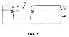
図7は、本発明に係る一実施形態におけるシャロー・トレンチを有する半導体基板の断面図を示す。シャロー・トレンチ40は、浅い注入領域24を介して半導体基板20内に異方性エッチングすることにより形成される。シャロー・トレンチ40は、半導体基板20内の側壁スペーサ26間の領域に形成される。角部注入領域27は、基板20の浅い注入領域24の一部分だけに残っている。開口部19を介して第2のハードマスク層25をエッチングすることによって、角部注入領域27の内縁が、第2のハードマスク層25の内縁と自己整合される。
FIG. 7 shows a cross-sectional view of a semiconductor substrate having a shallow trench in an embodiment according to the present invention. The
本発明に係る一実施形態では、シャロー・トレンチ40は、一般に、0.3〜0.5μmの深さと、0.15〜0.6μmの幅を有する。シャロー・トレンチ40の幅は、STI領域に使用される半導体基板の量を最少にするためにできるだけ小さくなければならない。STI領域のサイズを最小にすると、イメージ・センサ内の光検出領域に利用できる基板の量が増えて好都合である。
In one embodiment according to the present invention, the
図8を参照すると、シャロー・トレンチ40の側壁と底面に注入ドーパント28が注入される。本発明の一実施形態では、注入ドーパント28は、一般に、基板20の露出面から0〜100Åで注入され、注入ドーパント28の濃度は、一般に1012〜1013原子/cm2である。この注入は、通常、注入ドーパント28がシャロー・トレンチ40の4つの全ての側面と底面に注入されるように斜めに4回行われる(即ち、ウェーハが90度ずつ4回回転されて行われる)。
Referring to FIG. 8, implanted
注入ドーパント28は、角部注入領域27と同じ導電型である。本発明に係る一実施形態では、注入ドーパント28は、また浅い注入領域24のドーパントと同じドーパントである。注入ドーパント28は、燐、ヒ素、アンチモン等のn型ドーパントでもよく、又はホウ素、アルミニウム、ガリウム、インジウム等のp型ドーパントでもよい。
The implanted
誘電体(dielectric:絶縁体)層29は、一般に、ドーパント28が注入されたシリコン領域上に、減圧化学気相成長法、大気圧化学気相成長法、プラズマ化学気相成長法、又は高密度プラズマ堆積法によって形成される。誘電体層29に使用できる絶縁体の例には、内壁酸化物(liner oxide)又は窒化物があるがこれらに限定されない。絶縁体層29は、注入ドーパント28の注入前又は注入後に成長又は付着させることができる。次に、分離トレンチ40に誘電体(図示せず)が充填される。
A
図9aを参照すると、本発明に係る実施形態における側壁注入領域を有する2つのシャロウ・トレンチ・アイソレーション間にデバイスを有する半導体基板の第1の断面図が示される。STI領域42と43はそれぞれ、光検出領域30、31の隣りに示される。光検出領域30と31は、注入ドーパント28と角部注入領域27の導電型と反対の導電型を有する。転送ゲート32にパルス電圧が印加されたとき、1つの光検出領域(例えば、光検出領域30)から、ウェル34に含まれる浮動拡散領域33(検出ノードとも呼ばれる)内に電荷が転送される。次に、信号が、画素増幅器(図示せず)によって検出され、画素アレイの外側の下流回路(図示せず)に送られる。浮動拡散領域33は、注入ドーパント28と角部注入領域27の導電型と反対の導電型を有する。
Referring to FIG. 9a, a first cross-sectional view of a semiconductor substrate having a device between two shallow trench isolations having sidewall implant regions in an embodiment according to the present invention is shown.
図9bは、本発明に係る実施形態における側壁注入を有する2つのシャロウ・トレンチ・アイソレーション間にデバイスを含む半導体基板の第2の断面図を示す。角部注入領域27、注入ドーパント28、光検出領域30、31、浮動拡散33、ウェル34、及びピン留め層35、36の導電型は、図9aに示した導電型と反対にされる。
FIG. 9b shows a second cross-sectional view of a semiconductor substrate including a device between two shallow trench isolations with sidewall implants in an embodiment according to the present invention. The conductivity type of the
図9aと図9bに示した構造から第1のハードマスク層と第2のハードマスク層は除去された。しかしながら、最終構造でこれらの層が残ってもよいことは理解されたい。図9aと図9bに、2つの共用される光検出領域を備えたイメージ・センサを示したが、任意の数の光検出領域を使用できることを理解されたい。一般に、単一の浮動拡散領域に、転送ゲートによって、1つ、2つ又は4つの光検出領域を接続することができる。光検出領域は、通常、シャロー・トレンチより浅い深さに形成される。 The first hard mask layer and the second hard mask layer were removed from the structure shown in FIGS. 9a and 9b. However, it should be understood that these layers may remain in the final structure. Although FIGS. 9a and 9b show an image sensor with two shared light detection areas, it should be understood that any number of light detection areas can be used. In general, one, two or four photodetection regions can be connected to a single floating diffusion region by a transfer gate. The light detection region is usually formed at a depth shallower than the shallow trench.
10,20 半導体基板、11 酸化膜層、12,23 フォトレジスト・マスク、13,27 角部注入領域、14 側壁注入領域、18 フォトレジスト・マスクの開口部、19 第1のハードマスク層の開口部、21 エッチング停止層、22 第1のハードマスク層、24 浅い注入領域、25 第2のハードマスク層、26 側壁スペーサ、28 注入ドーパント、29 誘電体層、30,31 光検出領域、32 転送ゲート、33 浮動拡散、34 ウェル、35,36 ピン留め層、40 シャロー・トレンチ、42,43 シャロウ・トレンチ・アイソレーション。
DESCRIPTION OF
Claims (3)
第1のハードマスク層の開口部を介して第1のドーパントを注入することによって前記半導体基板の一部分に浅い注入領域を形成し、
前記半導体基板の浅い注入領域と前記第1のハードマスク層の上に第2のハードマスク層を形成し、
前記第2のハードマスク層をエッチングして前記第1のハードマスク層の前記側面に沿った側壁スペーサを形成し、各側壁スペーサが、前記半導体基板内の前記浅い注入領域の一部分に重なり、
前記側壁スペーサ間の前記半導体基板に対して、前記側壁スペーサに重なった前記浅い注入領域の一部分を残すようにエッチングすることで、その開口端に角部注入領域が形成されるとともに、前記浅い注入領域の前記半導体基板の厚さ方向の深さよりも深い、分離トレンチを形成し、
前記角部注入領域を残した状態で、前記分離トレンチの側壁と底壁に、前記角部注入領域と同じ導電型の第2のドーパントを注入することを含む方法。 A method for separating an element formed on a semiconductor substrate by forming an isolation region on the semiconductor substrate,
Forming a shallow implant region in a portion of the semiconductor substrate by implanting a first dopant through an opening in the first hard mask layer;
Forming a second hard mask layer over the shallow implantation region of the semiconductor substrate and the first hard mask layer;
Etching the second hard mask layer to form sidewall spacers along the side surfaces of the first hard mask layer, each sidewall spacer overlapping a portion of the shallow implantation region in the semiconductor substrate;
For the semiconductor substrate between the sidewall spacers, wherein by etching to leave a portion of the shallow implantation region overlapping the sidewall spacer, together with the corner implanted region at its open end is formed, the shallow implant Forming an isolation trench deeper than the depth of the region of the semiconductor substrate in the thickness direction ;
Implanting a second dopant of the same conductivity type as the corner implant region into the sidewall and bottom wall of the isolation trench, leaving the corner implant region .
前記半導体基板表面の上にエッチング停止層を形成し、
前記エッチング停止層の上に前記第1のハードマスク層を形成し、
前記第1のハードマスク層の上にフォトレジスト・マスク層を提供し、
前記フォトレジスト・マスク層をパターニングして前記フォトレジスト・マスク層に開口部を形成し、
前記フォトレジスト・マスク層の前記開口部を介して前記第1のハードマスク層をエッチングして前記第1のハードマスク層に前記開口部を形成する、方法。 The method of claim 1, further comprising:
Forming an etching stop layer on the surface of the semiconductor substrate;
Forming the first hard mask layer on the etch stop layer;
Providing a photoresist mask layer over the first hardmask layer;
Patterning the photoresist mask layer to form openings in the photoresist mask layer;
Etching the first hard mask layer through the opening in the photoresist mask layer to form the opening in the first hard mask layer;
Applications Claiming Priority (5)
| Application Number | Priority Date | Filing Date | Title |
|---|---|---|---|
| US84207506P | 2006-09-01 | 2006-09-01 | |
| US60/842,075 | 2006-09-01 | ||
| US11/840,299 US20080057612A1 (en) | 2006-09-01 | 2007-08-17 | Method for adding an implant at the shallow trench isolation corner in a semiconductor substrate |
| US11/840,299 | 2007-08-17 | ||
| PCT/US2007/018997 WO2008030371A2 (en) | 2006-09-01 | 2007-08-29 | Implant at shallow trench isolation corner |
Publications (3)
| Publication Number | Publication Date |
|---|---|
| JP2010503212A JP2010503212A (en) | 2010-01-28 |
| JP2010503212A5 JP2010503212A5 (en) | 2010-10-14 |
| JP5281008B2 true JP5281008B2 (en) | 2013-09-04 |
Family
ID=39031210
Family Applications (1)
| Application Number | Title | Priority Date | Filing Date |
|---|---|---|---|
| JP2009526696A Active JP5281008B2 (en) | 2006-09-01 | 2007-08-29 | Method for separating elements formed on a semiconductor substrate |
Country Status (7)
| Country | Link |
|---|---|
| US (1) | US20080057612A1 (en) |
| EP (1) | EP2057675B1 (en) |
| JP (1) | JP5281008B2 (en) |
| KR (1) | KR101329462B1 (en) |
| DE (1) | DE602007009548D1 (en) |
| TW (1) | TWI413167B (en) |
| WO (1) | WO2008030371A2 (en) |
Families Citing this family (20)
| Publication number | Priority date | Publication date | Assignee | Title |
|---|---|---|---|---|
| US20100148230A1 (en) * | 2008-12-11 | 2010-06-17 | Stevens Eric G | Trench isolation regions in image sensors |
| US7968424B2 (en) * | 2009-01-16 | 2011-06-28 | Taiwan Semiconductor Manufacturing Company, Ltd. | Method of implantation |
| US7838325B2 (en) * | 2009-02-13 | 2010-11-23 | Taiwan Semiconductor Manufacturing Company, Ltd. | Method to optimize substrate thickness for image sensor device |
| US9196547B2 (en) | 2009-04-03 | 2015-11-24 | Taiwan Semiconductor Manufacturing Company, Ltd. | Dual shallow trench isolation and related applications |
| US8048711B2 (en) * | 2009-12-30 | 2011-11-01 | Omnivision Technologies, Inc. | Method for forming deep isolation in imagers |
| US9000500B2 (en) | 2009-12-30 | 2015-04-07 | Omnivision Technologies, Inc. | Image sensor with doped transfer gate |
| US8367512B2 (en) | 2010-08-30 | 2013-02-05 | Taiwan Semiconductor Manufacturing Company, Ltd. | Self-aligned implants to reduce cross-talk of imaging sensors |
| FR2981502A1 (en) | 2011-10-18 | 2013-04-19 | St Microelectronics Crolles 2 | METHOD FOR PRODUCING AT LEAST ONE DEEP INSULATION TRENCH |
| US9040891B2 (en) * | 2012-06-08 | 2015-05-26 | Taiwan Semiconductor Manufacturing Company, Ltd. | Image device and methods of forming the same |
| US9355888B2 (en) | 2012-10-01 | 2016-05-31 | Taiwan Semiconductor Manufacturing Company, Ltd. | Implant isolated devices and method for forming the same |
| US9673245B2 (en) * | 2012-10-01 | 2017-06-06 | Taiwan Semiconductor Manufacturing Company, Ltd. | Implant isolated devices and method for forming the same |
| US8969997B2 (en) * | 2012-11-14 | 2015-03-03 | Taiwan Semiconductor Manufacturing Company, Ltd. | Isolation structures and methods of forming the same |
| WO2014209421A1 (en) * | 2013-06-29 | 2014-12-31 | Sionyx, Inc. | Shallow trench textured regions and associated methods |
| JP6362449B2 (en) | 2014-07-01 | 2018-07-25 | ルネサスエレクトロニクス株式会社 | Manufacturing method of semiconductor integrated circuit device |
| KR102399338B1 (en) * | 2014-09-12 | 2022-05-19 | 삼성전자주식회사 | Method of fabricating an image sensor same |
| US9647022B2 (en) * | 2015-02-12 | 2017-05-09 | Taiwan Semiconductor Manufacturing Co., Ltd. | Multi-layer structure for high aspect ratio etch |
| US10580789B2 (en) * | 2017-07-10 | 2020-03-03 | Macronix International Co., Ltd. | Semiconductor device having etching control layer in substrate and method of fabricating the same |
| CN109256389B (en) * | 2017-07-13 | 2021-06-11 | 旺宏电子股份有限公司 | Semiconductor device and method for manufacturing the same |
| CN110021559B (en) * | 2018-01-09 | 2021-08-24 | 联华电子股份有限公司 | Semiconductor element and manufacturing method thereof |
| US11923205B2 (en) * | 2021-12-17 | 2024-03-05 | United Microelectronics Corporation | Method for manufacturing semiconductor device |
Family Cites Families (27)
| Publication number | Priority date | Publication date | Assignee | Title |
|---|---|---|---|---|
| JPS6052580B2 (en) * | 1978-10-20 | 1985-11-20 | 三洋電機株式会社 | Manufacturing method for surface protective film in semiconductor devices |
| JPH01125935A (en) * | 1987-11-11 | 1989-05-18 | Seiko Instr & Electron Ltd | Manufacture of semiconductor device |
| JPH0621047A (en) * | 1992-05-08 | 1994-01-28 | Sanyo Electric Co Ltd | Semiconductor device and manufacture thereof |
| US5780353A (en) * | 1996-03-28 | 1998-07-14 | Advanced Micro Devices, Inc. | Method of doping trench sidewalls before trench etching |
| US5874346A (en) * | 1996-05-23 | 1999-02-23 | Advanced Micro Devices, Inc. | Subtrench conductor formation with large tilt angle implant |
| US5891787A (en) * | 1997-09-04 | 1999-04-06 | Advanced Micro Devices, Inc. | Semiconductor fabrication employing implantation of excess atoms at the edges of a trench isolation structure |
| US6030898A (en) * | 1997-12-19 | 2000-02-29 | Advanced Micro Devices, Inc. | Advanced etching method for VLSI fabrication |
| US6096612A (en) * | 1998-04-30 | 2000-08-01 | Texas Instruments Incorporated | Increased effective transistor width using double sidewall spacers |
| KR100372103B1 (en) * | 1998-06-30 | 2003-03-31 | 주식회사 하이닉스반도체 | Device Separation Method of Semiconductor Devices |
| TW391051B (en) * | 1998-11-06 | 2000-05-21 | United Microelectronics Corp | Method for manufacturing shallow trench isolation structure |
| TW406350B (en) * | 1998-12-07 | 2000-09-21 | United Microelectronics Corp | Method for manufacturing the shallow trench isolation area |
| TW486774B (en) * | 1998-12-19 | 2002-05-11 | United Microelectronics Corp | Shallow trench isolation technique joining field oxide layer |
| JP3425896B2 (en) * | 1999-06-15 | 2003-07-14 | Necエレクトロニクス株式会社 | Method for manufacturing semiconductor device |
| KR20010059185A (en) * | 1999-12-30 | 2001-07-06 | 박종섭 | A method for forming a field oxide of a semiconductor device |
| US6150235A (en) * | 2000-01-24 | 2000-11-21 | Worldwide Semiconductor Manufacturing Corp. | Method of forming shallow trench isolation structures |
| US6437417B1 (en) * | 2000-08-16 | 2002-08-20 | Micron Technology, Inc. | Method for making shallow trenches for isolation |
| US6624016B2 (en) * | 2001-02-22 | 2003-09-23 | Silicon-Based Technology Corporation | Method of fabricating trench isolation structures with extended buffer spacers |
| KR100438403B1 (en) * | 2001-09-05 | 2004-07-02 | 동부전자 주식회사 | Method for manufacturing a flat cell memory device |
| JP4087108B2 (en) * | 2001-12-10 | 2008-05-21 | シャープ株式会社 | Nonvolatile semiconductor memory device and manufacturing method thereof |
| KR100480897B1 (en) * | 2002-12-09 | 2005-04-07 | 매그나칩 반도체 유한회사 | Method for manufacturing STI of semiconductor device |
| US7102184B2 (en) * | 2003-06-16 | 2006-09-05 | Micron Technology, Inc. | Image device and photodiode structure |
| US7067387B2 (en) * | 2003-08-28 | 2006-06-27 | Taiwan Semiconductor Manufacturing Company | Method of manufacturing dielectric isolated silicon structure |
| US6951780B1 (en) * | 2003-12-18 | 2005-10-04 | Matrix Semiconductor, Inc. | Selective oxidation of silicon in diode, TFT, and monolithic three dimensional memory arrays |
| US7154136B2 (en) * | 2004-02-20 | 2006-12-26 | Micron Technology, Inc. | Isolation structures for preventing photons and carriers from reaching active areas and methods of formation |
| US7279397B2 (en) * | 2004-07-27 | 2007-10-09 | Texas Instruments Incorporated | Shallow trench isolation method |
| US7045410B2 (en) * | 2004-07-27 | 2006-05-16 | Texas Instruments Incorporated | Method to design for or modulate the CMOS transistor threshold voltage using shallow trench isolation (STI) |
| US7262110B2 (en) * | 2004-08-23 | 2007-08-28 | Micron Technology, Inc. | Trench isolation structure and method of formation |
-
2007
- 2007-08-17 US US11/840,299 patent/US20080057612A1/en not_active Abandoned
- 2007-08-29 KR KR1020097004162A patent/KR101329462B1/en active IP Right Grant
- 2007-08-29 DE DE602007009548T patent/DE602007009548D1/en active Active
- 2007-08-29 WO PCT/US2007/018997 patent/WO2008030371A2/en active Application Filing
- 2007-08-29 JP JP2009526696A patent/JP5281008B2/en active Active
- 2007-08-29 EP EP07837483A patent/EP2057675B1/en active Active
- 2007-08-31 TW TW096132663A patent/TWI413167B/en active
Also Published As
| Publication number | Publication date |
|---|---|
| WO2008030371A3 (en) | 2008-04-17 |
| JP2010503212A (en) | 2010-01-28 |
| US20080057612A1 (en) | 2008-03-06 |
| TW200830381A (en) | 2008-07-16 |
| KR20090045294A (en) | 2009-05-07 |
| WO2008030371A2 (en) | 2008-03-13 |
| DE602007009548D1 (en) | 2010-11-11 |
| KR101329462B1 (en) | 2013-11-13 |
| EP2057675B1 (en) | 2010-09-29 |
| TWI413167B (en) | 2013-10-21 |
| EP2057675A2 (en) | 2009-05-13 |
Similar Documents
| Publication | Publication Date | Title |
|---|---|---|
| JP5281008B2 (en) | Method for separating elements formed on a semiconductor substrate | |
| US8482094B2 (en) | Semiconductor device and method for fabricating the same | |
| JP5318955B2 (en) | Shallow trench isolation structure having air gap, CMOS image sensor using the same, and method for manufacturing CMOS image sensor | |
| EP1213757B1 (en) | Integrated circuits having adjacent p-type doped regions having shallow trench isolation structures without liner layers therebetween and methods of forming same | |
| US20060276014A1 (en) | Self-aligned high-energy implantation for deep junction structure | |
| US8440540B2 (en) | Method for doping a selected portion of a device | |
| TWI613816B (en) | Semiconductor device and methods for forming the same | |
| US11705475B2 (en) | Method of forming shallow trench isolation (STI) structure for suppressing dark current | |
| KR100425462B1 (en) | Semiconductor device on SOI(silicon on insulator) structure) and method for manufacturing the same | |
| JP2013065862A (en) | Method for fabricating cmos image sensor protecting photodiode from plasma damage | |
| US7429496B2 (en) | Buried photodiode for image sensor with shallow trench isolation technology | |
| US8987033B2 (en) | Method for forming CMOS image sensors | |
| CN113224089A (en) | Shallow Trench Isolation (STI) structure for CMOS image sensor | |
| CN116110920A (en) | Method for manufacturing semiconductor structure and semiconductor structure | |
| CN101512752A (en) | Implant at shallow trench isolation corner | |
| US20090170276A1 (en) | Method of Forming Trench of Semiconductor Device | |
| KR100246197B1 (en) | Method for isolating semiconductor | |
| KR100359162B1 (en) | Method for manufacturing transistor | |
| JP2006216604A (en) | Semiconductor device and manufacturing method thereof | |
| KR100474588B1 (en) | Device isolation method of semiconductor device | |
| KR101044773B1 (en) | MOS transistor and method for manufacturing MOS transistor increased channel width | |
| KR100700283B1 (en) | Method of fabricating the trench for isolation in semiconductor device | |
| KR20090021465A (en) | Producing method of non-silicide | |
| KR20020017105A (en) | Method for isolating semiconductor devices | |
| KR20100109141A (en) | Method for fabricaing partial silicon on insulator substrate |
Legal Events
| Date | Code | Title | Description |
|---|---|---|---|
| A521 | Request for written amendment filed |
Free format text: JAPANESE INTERMEDIATE CODE: A523 Effective date: 20100824 |
|
| A621 | Written request for application examination |
Free format text: JAPANESE INTERMEDIATE CODE: A621 Effective date: 20100824 |
|
| A521 | Request for written amendment filed |
Free format text: JAPANESE INTERMEDIATE CODE: A523 Effective date: 20110725 |
|
| A711 | Notification of change in applicant |
Free format text: JAPANESE INTERMEDIATE CODE: A711 Effective date: 20110725 |
|
| A131 | Notification of reasons for refusal |
Free format text: JAPANESE INTERMEDIATE CODE: A131 Effective date: 20130205 |
|
| A521 | Request for written amendment filed |
Free format text: JAPANESE INTERMEDIATE CODE: A523 Effective date: 20130409 |
|
| TRDD | Decision of grant or rejection written | ||
| A01 | Written decision to grant a patent or to grant a registration (utility model) |
Free format text: JAPANESE INTERMEDIATE CODE: A01 Effective date: 20130507 |
|
| A61 | First payment of annual fees (during grant procedure) |
Free format text: JAPANESE INTERMEDIATE CODE: A61 Effective date: 20130523 |
|
| R150 | Certificate of patent or registration of utility model |
Ref document number: 5281008 Country of ref document: JP Free format text: JAPANESE INTERMEDIATE CODE: R150 Free format text: JAPANESE INTERMEDIATE CODE: R150 |
|
| R250 | Receipt of annual fees |
Free format text: JAPANESE INTERMEDIATE CODE: R250 |
|
| R250 | Receipt of annual fees |
Free format text: JAPANESE INTERMEDIATE CODE: R250 |
|
| R250 | Receipt of annual fees |
Free format text: JAPANESE INTERMEDIATE CODE: R250 |
|
| R250 | Receipt of annual fees |
Free format text: JAPANESE INTERMEDIATE CODE: R250 |
|
| R250 | Receipt of annual fees |
Free format text: JAPANESE INTERMEDIATE CODE: R250 |
|
| R250 | Receipt of annual fees |
Free format text: JAPANESE INTERMEDIATE CODE: R250 |
|
| R250 | Receipt of annual fees |
Free format text: JAPANESE INTERMEDIATE CODE: R250 |
|
| R250 | Receipt of annual fees |
Free format text: JAPANESE INTERMEDIATE CODE: R250 |