JP5250949B2 - Light emitting element module - Google Patents
Light emitting element module Download PDFInfo
- Publication number
- JP5250949B2 JP5250949B2 JP2006215120A JP2006215120A JP5250949B2 JP 5250949 B2 JP5250949 B2 JP 5250949B2 JP 2006215120 A JP2006215120 A JP 2006215120A JP 2006215120 A JP2006215120 A JP 2006215120A JP 5250949 B2 JP5250949 B2 JP 5250949B2
- Authority
- JP
- Japan
- Prior art keywords
- resin material
- sealing
- sealing resin
- emitting element
- light emitting
- Prior art date
- Legal status (The legal status is an assumption and is not a legal conclusion. Google has not performed a legal analysis and makes no representation as to the accuracy of the status listed.)
- Active
Links
Images


Classifications
-
- H—ELECTRICITY
- H01—ELECTRIC ELEMENTS
- H01L—SEMICONDUCTOR DEVICES NOT COVERED BY CLASS H10
- H01L33/00—Semiconductor devices with at least one potential-jump barrier or surface barrier specially adapted for light emission; Processes or apparatus specially adapted for the manufacture or treatment thereof or of parts thereof; Details thereof
- H01L33/48—Semiconductor devices with at least one potential-jump barrier or surface barrier specially adapted for light emission; Processes or apparatus specially adapted for the manufacture or treatment thereof or of parts thereof; Details thereof characterised by the semiconductor body packages
- H01L33/52—Encapsulations
- H01L33/56—Materials, e.g. epoxy or silicone resin
-
- H—ELECTRICITY
- H01—ELECTRIC ELEMENTS
- H01L—SEMICONDUCTOR DEVICES NOT COVERED BY CLASS H10
- H01L2224/00—Indexing scheme for arrangements for connecting or disconnecting semiconductor or solid-state bodies and methods related thereto as covered by H01L24/00
- H01L2224/01—Means for bonding being attached to, or being formed on, the surface to be connected, e.g. chip-to-package, die-attach, "first-level" interconnects; Manufacturing methods related thereto
- H01L2224/42—Wire connectors; Manufacturing methods related thereto
- H01L2224/44—Structure, shape, material or disposition of the wire connectors prior to the connecting process
- H01L2224/45—Structure, shape, material or disposition of the wire connectors prior to the connecting process of an individual wire connector
- H01L2224/45001—Core members of the connector
- H01L2224/45099—Material
- H01L2224/451—Material with a principal constituent of the material being a metal or a metalloid, e.g. boron (B), silicon (Si), germanium (Ge), arsenic (As), antimony (Sb), tellurium (Te) and polonium (Po), and alloys thereof
- H01L2224/45138—Material with a principal constituent of the material being a metal or a metalloid, e.g. boron (B), silicon (Si), germanium (Ge), arsenic (As), antimony (Sb), tellurium (Te) and polonium (Po), and alloys thereof the principal constituent melting at a temperature of greater than or equal to 950°C and less than 1550°C
- H01L2224/45144—Gold (Au) as principal constituent
-
- H—ELECTRICITY
- H01—ELECTRIC ELEMENTS
- H01L—SEMICONDUCTOR DEVICES NOT COVERED BY CLASS H10
- H01L2224/00—Indexing scheme for arrangements for connecting or disconnecting semiconductor or solid-state bodies and methods related thereto as covered by H01L24/00
- H01L2224/01—Means for bonding being attached to, or being formed on, the surface to be connected, e.g. chip-to-package, die-attach, "first-level" interconnects; Manufacturing methods related thereto
- H01L2224/42—Wire connectors; Manufacturing methods related thereto
- H01L2224/47—Structure, shape, material or disposition of the wire connectors after the connecting process
- H01L2224/48—Structure, shape, material or disposition of the wire connectors after the connecting process of an individual wire connector
- H01L2224/481—Disposition
- H01L2224/48151—Connecting between a semiconductor or solid-state body and an item not being a semiconductor or solid-state body, e.g. chip-to-substrate, chip-to-passive
- H01L2224/48221—Connecting between a semiconductor or solid-state body and an item not being a semiconductor or solid-state body, e.g. chip-to-substrate, chip-to-passive the body and the item being stacked
- H01L2224/48245—Connecting between a semiconductor or solid-state body and an item not being a semiconductor or solid-state body, e.g. chip-to-substrate, chip-to-passive the body and the item being stacked the item being metallic
- H01L2224/48247—Connecting between a semiconductor or solid-state body and an item not being a semiconductor or solid-state body, e.g. chip-to-substrate, chip-to-passive the body and the item being stacked the item being metallic connecting the wire to a bond pad of the item
-
- H—ELECTRICITY
- H01—ELECTRIC ELEMENTS
- H01L—SEMICONDUCTOR DEVICES NOT COVERED BY CLASS H10
- H01L2924/00—Indexing scheme for arrangements or methods for connecting or disconnecting semiconductor or solid-state bodies as covered by H01L24/00
- H01L2924/15—Details of package parts other than the semiconductor or other solid state devices to be connected
- H01L2924/181—Encapsulation
-
- H—ELECTRICITY
- H01—ELECTRIC ELEMENTS
- H01L—SEMICONDUCTOR DEVICES NOT COVERED BY CLASS H10
- H01L2924/00—Indexing scheme for arrangements or methods for connecting or disconnecting semiconductor or solid-state bodies as covered by H01L24/00
- H01L2924/30—Technical effects
- H01L2924/301—Electrical effects
- H01L2924/3025—Electromagnetic shielding
-
- H—ELECTRICITY
- H01—ELECTRIC ELEMENTS
- H01L—SEMICONDUCTOR DEVICES NOT COVERED BY CLASS H10
- H01L33/00—Semiconductor devices with at least one potential-jump barrier or surface barrier specially adapted for light emission; Processes or apparatus specially adapted for the manufacture or treatment thereof or of parts thereof; Details thereof
- H01L33/48—Semiconductor devices with at least one potential-jump barrier or surface barrier specially adapted for light emission; Processes or apparatus specially adapted for the manufacture or treatment thereof or of parts thereof; Details thereof characterised by the semiconductor body packages
- H01L33/52—Encapsulations
- H01L33/54—Encapsulations having a particular shape
-
- H—ELECTRICITY
- H01—ELECTRIC ELEMENTS
- H01L—SEMICONDUCTOR DEVICES NOT COVERED BY CLASS H10
- H01L33/00—Semiconductor devices with at least one potential-jump barrier or surface barrier specially adapted for light emission; Processes or apparatus specially adapted for the manufacture or treatment thereof or of parts thereof; Details thereof
- H01L33/48—Semiconductor devices with at least one potential-jump barrier or surface barrier specially adapted for light emission; Processes or apparatus specially adapted for the manufacture or treatment thereof or of parts thereof; Details thereof characterised by the semiconductor body packages
- H01L33/58—Optical field-shaping elements
-
- H—ELECTRICITY
- H01—ELECTRIC ELEMENTS
- H01L—SEMICONDUCTOR DEVICES NOT COVERED BY CLASS H10
- H01L33/00—Semiconductor devices with at least one potential-jump barrier or surface barrier specially adapted for light emission; Processes or apparatus specially adapted for the manufacture or treatment thereof or of parts thereof; Details thereof
- H01L33/48—Semiconductor devices with at least one potential-jump barrier or surface barrier specially adapted for light emission; Processes or apparatus specially adapted for the manufacture or treatment thereof or of parts thereof; Details thereof characterised by the semiconductor body packages
- H01L33/62—Arrangements for conducting electric current to or from the semiconductor body, e.g. lead-frames, wire-bonds or solder balls
Abstract
Description
本発明は、基体上で発光素子を樹脂封止した発光素子モジュール及びその製造方法に関する。 The present invention relates to a light emitting element module in which a light emitting element is sealed with a resin on a substrate and a method for manufacturing the same.
発光ダイオード(LED)等の発光素子は、低消費電力、小型、軽量等の特徴を有し、それを樹脂封止したものは、各種表示灯等に用いられているが、近年青色LED、白色LEDが開発され、高輝度化も進んだことから、液晶表示パネル用のバックライト用光源、照明用光源、信号灯等への応用が急速に進み、自動車のヘッドライトへの応用も開発されている。 Light emitting elements such as light emitting diodes (LEDs) have features such as low power consumption, small size, and light weight, and those sealed with resin are used in various display lamps, etc. As LEDs have been developed and their brightness has been increased, their application to backlight light sources, illumination light sources, signal lights, etc. for liquid crystal display panels is rapidly progressing, and applications for automobile headlights are also being developed. .
従来、LEDの封止材としては、屈折率が1.53〜1.57のビスフェノールAグリシジルエーテル型エポキシ樹脂が使用されている。しかしながら、LEDの高輝度化に伴い、LED作動時の温度が上がり、封止材も高温や高輝度の光に曝されるようになると、従来のエポキシ樹脂からなる封止材は耐熱性と耐光性(特に、UVや青色光に対する耐光性)が不十分となって変色を起こすようになり、LEDの輝度が経時的に低下するという問題がある。この問題に対しては、高透明性のエポキシ樹脂が開発されているが、未だ、十分な耐熱性や耐光性を得るには至っていない。 Conventionally, a bisphenol A glycidyl ether type epoxy resin having a refractive index of 1.53 to 1.57 has been used as an LED sealing material. However, as the brightness of LEDs increases and the temperature during LED operation increases and the encapsulant is exposed to high temperature and high intensity light, the conventional encapsulant made of epoxy resin is resistant to heat and light. There is a problem that the property (particularly, light resistance to UV and blue light) becomes insufficient and discoloration occurs, and the luminance of the LED decreases with time. To solve this problem, highly transparent epoxy resins have been developed, but sufficient heat resistance and light resistance have not yet been obtained.
これに対し、ゲルタイプのシリコーン樹脂が高輝度LEDに使用されるようになっている。このシリコーン樹脂によれば、エポキシ樹脂に比して耐熱性や耐光性が向上し、さらにゲルタイプであることにより熱応力によるチップの劣化を回避することができる。しかしながら、ゲルタイプのシリコーン樹脂は、硬化後、表面にべたつきがあり、ゴミや埃がつきやすく、また表面に傷もつきやすいため、それを表層として用いるには問題がある。 On the other hand, a gel type silicone resin is used for high-brightness LEDs. According to this silicone resin, heat resistance and light resistance are improved as compared with an epoxy resin, and further, deterioration of the chip due to thermal stress can be avoided by being a gel type. However, the gel type silicone resin has a stickiness on the surface after curing, is liable to be dusty and dusty, and is susceptible to scratches on the surface, and there is a problem in using it as a surface layer.
一方、発光素子を樹脂封止した発光素子モジュールにおいて、発光素子が発した光が封止樹脂と空気との界面で全反射することを防止して光の取り出し効率を上げるため、封止材の外形をドーム形とし、封止材にレンズ機能を付与することがなされている。例えば、環状オレフィン共重合体等の透明樹脂を用いて射出成型法によりドーム形封止材を形成し、この中にゲルタイプのシリコーン樹脂を注入し、その内側の空洞内にLEDチップを固定したものが提案されている(特許文献1)。 On the other hand, in a light emitting element module in which the light emitting element is resin-sealed, the light emitted from the light emitting element is prevented from being totally reflected at the interface between the sealing resin and air, and the light extraction efficiency is increased. The outer shape is a dome shape, and a lens function is imparted to the sealing material. For example, a dome-shaped sealing material is formed by an injection molding method using a transparent resin such as a cyclic olefin copolymer, a gel type silicone resin is injected therein, and an LED chip is fixed in a cavity inside the sealing material. The thing is proposed (patent document 1).
また、基体凹部にLEDベアチップを固定し、その上にゲルタイプのシリコーン樹脂を塗布して硬化させ、一方、ドーム状に中抜となっている型枠内にエポキシ樹脂を充填し、そこにシリコーン樹脂で封止したLEDを被せるように挿入し、型枠内のエポキシ樹脂を硬化させる方法が知られている(特許文献2)。 In addition, the LED bare chip is fixed to the concave portion of the base, and a gel type silicone resin is applied and cured on the LED bare chip. On the other hand, an epoxy resin is filled in a mold that is hollowed out in a dome shape. A method of inserting an LED sealed with a resin so as to cover it and curing an epoxy resin in a mold is known (Patent Document 2).
上述の先行技術では、封止材を2層とし、その第2の封止材(外側)として、タックがなく、硬度の高い材料を用いることで、表面にべたつきが生じ易く、また傷がつき易いというシリコーン樹脂特有の問題を解決している。 In the above-described prior art, the sealing material has two layers, and the second sealing material (outside) is made of a material having no tack and high hardness, so that the surface is easily sticky and scratched. It solves the problem peculiar to silicone resin that it is easy.
しかしながら、上述したいずれの方法においても、LEDベアチップを直接封止する封止材と、ドーム形に成形した封止材との界面でLEDから発した光が反射し、光の取り出し効率を確実に高めることができない。 However, in any of the above-described methods, the light emitted from the LED is reflected at the interface between the sealing material that directly seals the LED bare chip and the sealing material that is molded into a dome shape, thereby ensuring the light extraction efficiency. It cannot be increased.
このような従来技術の問題点に対し、本発明は、LED等の発光素子を直接封止する第1の封止材と、その外側を封止する第2の封止材からなる発光素子モジュールにおいて、(1)第1の封止材と第2の封止材との界面における反射を防止し、発光素子からの光の取り出し効率を向上させること、(2)封止材中に気泡が含まれないようにすること、さらには、(3)封止材がレンズ機能を有する発光素子モジュールを、型枠を使用せず簡便にコンパクトに製造できるようにすることを目的とする。 In order to solve such problems of the prior art, the present invention provides a light emitting element module comprising a first sealing material that directly seals a light emitting element such as an LED, and a second sealing material that seals the outside thereof. In (1), the reflection at the interface between the first sealing material and the second sealing material is prevented, the light extraction efficiency from the light emitting element is improved, and (2) bubbles are present in the sealing material. Further, it is intended to make it possible to easily and compactly manufacture a light emitting element module whose sealing material has a lens function without using a mold.
本発明者らは、LED等の発光素子が第1の封止材と第2の封止材で順次封止されている発光素子モジュールを製造するにあたり、発光素子上に第1の封止樹脂材料と第2の封止樹脂材料を順次塗布し、それらが完全には硬化していない状態で、双方の封止樹脂材料の界面にぼかし処理を行い、その後これらを硬化させて発光素子モジュールとすることにより、第1の封止材と第2の封止材のぼかされた界面で屈折率が連続的に変化するので、第1の封止材と第2の封止材との界面における反射を防止でき、これにより光の取り出し効率を向上させられること、また、この方法によれば、真空脱泡により気泡を除去できること、さらに、発光素子を搭載する基体を撥油処理することにより、型枠を使用することなく封止樹脂材料をドーム型に成形でき、封止材にレンズ機能を付与できることを見出し、本発明を完成させた。 In producing a light emitting element module in which light emitting elements such as LEDs are sequentially sealed with a first sealing material and a second sealing material, the first sealing resin is formed on the light emitting elements. The material and the second sealing resin material are sequentially applied, and in a state where they are not completely cured, the interface between both the sealing resin materials is subjected to a blurring treatment, and thereafter, these are cured to obtain a light emitting element module. By doing so, since the refractive index continuously changes at the blurred interface between the first sealing material and the second sealing material, the interface between the first sealing material and the second sealing material In this method, it is possible to improve the light extraction efficiency, and according to this method, it is possible to remove bubbles by vacuum defoaming, and furthermore, by subjecting the substrate on which the light emitting element is mounted to an oil repellent treatment , Sealing resin material into dome shape without using formwork Can form, it found that a lens function can be imparted to the sealing material, thereby completing the present invention.
即ち、本発明は、基体上の発光素子に第1の封止材及び第2の封止材が順次積層されている発光素子モジュールであって、第1の封止材と第2の封止材との界面にぼかし処理が施されている発光素子モジュール提供する。 That is, the present invention is a light emitting element module in which a first sealing material and a second sealing material are sequentially laminated on a light emitting element on a substrate, and the first sealing material and the second sealing material are stacked. Provided is a light emitting element module in which an interface with a material is subjected to a blurring process.
また、本発明は、基体に発光素子を搭載し、その上に、第1の封止材の未硬化物である第1の封止樹脂材料、及び第2の封止材の未硬化物である第2の封止樹脂材料を順次塗布し、室温〜120℃で数分〜数時間おくアニーリングを行うことにより第1の封止樹脂材料と第2の封止樹脂材料の界面をぼかし、その後、第1の封止樹脂材料と第2の封止樹脂材料を完全に硬化させる発光素子モジュールの製造方法を提供する。 In the present invention, the light emitting element is mounted on the base, and the first sealing resin material that is an uncured material of the first sealing material and the uncured material of the second sealing material are mounted thereon. A certain second sealing resin material is sequentially applied and annealed at room temperature to 120 ° C. for several minutes to several hours to blur the interface between the first sealing resin material and the second sealing resin material, and thereafter A method for manufacturing a light-emitting element module is provided in which a first sealing resin material and a second sealing resin material are completely cured.
本発明の発光素子モジュールによれば、発光素子を封止する第1の封止材と第2の封止材の界面にぼかし処理が施されているので、そのぼかされた界面で第1の封止材と第2の封止材の屈折率が連続的に変化し、発光素子から発した光が第1の封止材と第2の封止材との界面で反射することを防止できる。したがって、発光素子モジュールの光の取り出し効率を向上させることができる。 According to the light emitting element module of the present invention, the blurring process is applied to the interface between the first sealing material and the second sealing material that seals the light emitting element. The refractive index of the sealing material and the second sealing material are continuously changed, and light emitted from the light emitting element is prevented from being reflected at the interface between the first sealing material and the second sealing material. it can. Therefore, the light extraction efficiency of the light emitting element module can be improved.
また、本発明の発光素子モジュールの製造方法によれば、第1の封止材と第2の封止材の界面を確実にかつ容易にぼかすことがきる。 Moreover, according to the manufacturing method of the light emitting element module of this invention, the interface of a 1st sealing material and a 2nd sealing material can be blurred reliably and easily.
さらに、この製造方法によれば、第1の封止材の未硬化物である第1の封止樹脂材料を、硬化物済みの第2の封止材と発光素子の基体との間に注入せず、第1の封止樹脂材料と第2の封止樹脂材料を順次塗布後、それらを硬化させるので、第1の封止樹脂材料中に気泡が生じても、第1の封止樹脂材料の硬化前に真空脱泡を行うことにより容易に気泡を除去することができる。 Furthermore, according to this manufacturing method, the first sealing resin material, which is an uncured material of the first sealing material, is injected between the cured second material and the substrate of the light emitting element. Without applying the first sealing resin material and the second sealing resin material in sequence, the first sealing resin material and the second sealing resin material are cured, so that even if air bubbles are generated in the first sealing resin material, Air bubbles can be easily removed by performing vacuum defoaming before the material is cured.
また、基体表面において、第1の封止材の周縁部を囲む領域及び第2の封止材の周縁部を囲む領域に、それぞれ環状凸部を設け、また、発光素子を囲む領域に撥油処理を施しておくと、型枠を使用することなく、封止樹脂材料をドーム形に成形することが可能となり、簡便な製法で発光素子モジュールの光の取り出し効率を一層向上させることが可能となる。 In addition, on the surface of the substrate, annular convex portions are respectively provided in a region surrounding the peripheral portion of the first sealing material and a region surrounding the peripheral portion of the second sealing material, and an oil repellent is provided in the region surrounding the light emitting element. If the treatment is performed, the sealing resin material can be formed into a dome shape without using a mold, and the light extraction efficiency of the light emitting element module can be further improved by a simple manufacturing method. Become.
以下、本発明を図面を参照しつつ詳細に説明する。なお、各図中、同一符号は同一又は同等の構成要素を表している。 Hereinafter, the present invention will be described in detail with reference to the drawings. In each figure, the same numerals indicate the same or equivalent components.
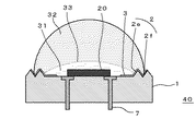
図1は、本発明の発光素子モジュールの一態様であるLEDモジュール40の断面図である。このLEDモジュール40は、基体1に接着固定されたLEDベアチップ20上に第1の封止材31及び第2の封止材32が順次積層されたものであり、この第1の封止材31と第2の封止材32との界面33にぼかし処理が施されていることを特徴としている。ここで界面33にぼかし処理が施されているとは、第1の封止材31と第2の封止材32との間に明瞭な界面が存在しないこと、即ち、第1の封止材31と第2の封止材のぼかされた界面で屈折率が連続的に変化していることをいう。この界面33のぼかし処理により、LEDベアチップ20から発した光が第1の封止材31と第2の封止材32との界面33で反射することを防止し、より多くの光をLEDモジュール40の外に取り出すことが可能となる。なお、図中、符号7は、LEDベアチップ20の電極端子に接続するリード電極である。
FIG. 1 is a cross-sectional view of an
このLEDモジュール40の製造方法としては、例えば、まず基体1にLEDベアチップ20を接着固定することにより搭載し、次に、LEDベアチップ20上に、第1の封止材の未硬化物である第1の封止樹脂材料を塗布することによりLEDベアチップ20を覆い、次いで、第1の封止樹脂材料を完全硬化させることなく、第1の封止樹脂材料上に、第2の封止材の未硬化物である第2の封止樹脂材料を塗布し、ひきつづき、アニーリングを行って第1の封止樹脂材料と第2の封止樹脂材料との界面をぼかし、その後、第1の封止樹脂材料と第2の封止樹脂材料を完全に硬化させ、LEDモジュール40とする。
As a manufacturing method of the
ここで、基体1としては、特に制限はなく、従来よりLEDの基体として使用されているABS樹脂、ポリフタルアミド等のエンジニアリングプラスチックの射出成型体を使用することができる。この成型体の内部には、リード電極やヒートシンクを内蔵させることができる。また、基体1としては、このような成型体に代えて、リジッド基板やフレキシブル基板を使用することもできる。
Here, there is no restriction | limiting in particular as the base |
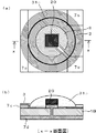
基体1の表面には、第1の封止材31の周縁部及び第2の封止材32の周縁部を囲む領域に、環状凸部2を形成しておくことが好ましい。これにより、第1の封止樹脂材料や第2の封止樹脂材料が基体1の表面に流れ広がることを防止できる。環状凸部2の具体的な形状は、例えば、図1に示すように、基体1の底面に対して起立した第1の垂直面2aと第2の垂直面2bを有する二重の段差形状としてもよく、図2に示すように、基体1の底面に対して起立した第1の斜面2cと第2の斜面2dを有する二重の段差形状としてもよく、図3に示すように、断面三角形又は矩形の環状凸部2e、2fを隣接させて二重に設けてもよく、図4に示すように、断面三角形又は矩形の環状凸部2g、2hを間隙をおいて二重に設けてもよい。また、図5に示すように、単一の斜面を有する環状凸部2iを設けてもよい。中でも、環状凸部2としては、構造が単純な点から、図5のように単一斜面を形成することが好ましい。
On the surface of the
また、基体1の表面のLEDの搭載部位を囲む領域には、第1の封止樹脂材料及び第2の封止樹脂材料の塗布前に予め撥油処理層3を設け、基体表面の界面張力を低めることが好ましい。これにより、これら封止樹脂材料が基体1の表面に流れ広がることを防止できる。特に、図6に示すように、平坦で環状凸部のない基体1を使用する場合には、この撥油処理が必須である。さらに、第1の封止材31及び第2の封止材32を、それぞれ型枠を使用することなく、ドーム形(即ち盾状から半球状)に形成することが可能となる。
Also, an oil
撥油処理層3は、基体1の表面に、表面張力の低い撥油剤を塗布し、その被膜を形成することにより設けることができる。ここで、撥油剤としてはフッ素系樹脂が好ましく、これを溶剤で希釈し、塗布、乾燥させることにより簡便に撥油剤の被膜を形成することができる。
The oil
フッ素系樹脂の代表例としては、パーフルオロアルキルアクリレートもしくはメタクリレート(アルキル基の炭素数6〜9)のホモポリマーをあげることができる。このホモポリマーは、フッ素系溶剤に溶解させて使用する。また、撥油剤としては、パーフルオロアルキルアクリレートとラウリルアクリレート等の共重合体も使用することができる。この共重合体は、トルエン、メチルエチルケトン等の汎用溶媒を用いて希釈することができる。 As a typical example of the fluororesin, a homopolymer of perfluoroalkyl acrylate or methacrylate (alkyl group having 6 to 9 carbon atoms) can be given. This homopolymer is used after being dissolved in a fluorinated solvent. As the oil repellent, a copolymer such as perfluoroalkyl acrylate and lauryl acrylate can also be used. This copolymer can be diluted using a general-purpose solvent such as toluene or methyl ethyl ketone.
なお、基体1の表面の撥油剤の塗布領域は、環状凸部2も含めてLEDの搭載部位を囲む領域とすることができるが、LEDの搭載部位には塗布しないようにする。LEDの搭載部位に撥油剤を塗布すると、そこにLEDベアチップを接着固定することが難しくなる。また、LEDベアチップ20の表面に塗布すると、撥油剤の屈折率が低いため光取り出し効率が悪くなる。
In addition, although the application | coating area | region of the lube repellant on the surface of the base |
第1の封止樹脂材料としては、その硬化物(即ち第1の封止材31)の硬度が、硬くないものが好ましく、より具体的には、ショアA硬度で70以下が好ましい。これにより、LEDモジュール40においてLEDベアチップ20と第1の封止材31との間に生じる熱応力を緩和することができ、LEDベアチップ20の発光寿命を大幅に伸ばすことが可能となる。第1の封止材31の硬度の下限については特に制限はなく、柔らかいゲル状であってもよい。
As the first sealing resin material, a hardened material (that is, the first sealing material 31) is preferably not hard, and more specifically, the Shore A hardness is preferably 70 or less. Thereby, the thermal stress which arises between the LED
第1の封止樹脂材料の粘度は、25℃で50Pa・S以下が好ましく、より好ましくは10Pa・S以下である。これにより、第1の封止樹脂材料をLEDベアチップ20上に塗布する際に気泡が発生し難くなり、また、気泡が発生した場合でも、その気泡を真空脱泡等で効果的に除去することができる。
The viscosity of the first sealing resin material is preferably 50 Pa · S or less at 25 ° C., more preferably 10 Pa · S or less. This makes it difficult for bubbles to be generated when the first sealing resin material is applied onto the LED
第1の封止樹脂材料の硬化物である第1の封止材31の屈折率は、光取り出し効率の点から、LEDベアチップの基板の屈折率(サファイア基板の場合1.76)と第2の封止材32の屈折率との間の1.40〜1.76とすることが好ましい。したがって、その未硬化物である第1の封止樹脂材料の屈折率としては、これよりも屈折率が0.01〜0.03低いものを使用することが好ましい。通常、硬化させることで屈折率は0.01〜0.03上昇するからである。
The refractive index of the
上述の硬度、粘度、屈折率の点から、第1の封止樹脂材料の好適な樹脂の種類としては、シリコーン樹脂、アクリル樹脂、メタクリル樹脂、ウレタン樹脂、エポキシ樹脂等をあげることができ、特に、シリコーン樹脂、アクリル樹脂、メタクリル樹脂が好ましい。 In view of the above-mentioned hardness, viscosity, and refractive index, examples of suitable resins for the first sealing resin material include silicone resins, acrylic resins, methacrylic resins, urethane resins, and epoxy resins. Silicone resin, acrylic resin, and methacrylic resin are preferable.
また、第1の封止樹脂材料には、必要に応じて、消泡剤、重合禁止剤、重合開始剤等の添加剤を加えることができる。 Moreover, additives, such as an antifoamer, a polymerization inhibitor, and a polymerization initiator, can be added to the first sealing resin material as necessary.
第1の封止樹脂材料のLEDベアチップ20上への塗布方法としては、例えば、シリンジ、ディスペンサー等を用い、ドーム型に盛りつけすることが好ましい。
As a method for applying the first sealing resin material onto the LED
第1の封止樹脂材料をLEDベアチップ20上へ塗布した後は、必要に応じて脱泡処理を行う。即ち、第1の封止樹脂材料として、低粘度の樹脂を使用し、さらに消泡剤を添加した場合でも、LEDベアチップ20自体の段差部、LEDベアチップ20と基体1との接合部周辺、LEDベアチップ20と電極との接合部周辺、ボンディングワイヤーの周囲等では、気泡が発生することを完全になくすことは難しい。そこで、脱泡処理により封止樹脂中あるいはその表面に発生した気泡を除去する。
After apply | coating the 1st sealing resin material on the LED
脱泡処理としては、脱泡効果の点から真空脱泡が好ましい。真空脱泡は、第1の封止樹脂材料を塗布した後、これを真空チャンバーなどの中で真空にすることにより気泡を膨張、破裂させる処理である。本発明では、第1の封止樹脂材料をLEDベアチップ20上に塗布した時点で、その第1の封止樹脂材料が第2の封止樹脂材料の硬化物(第2の封止材32)で覆われていないので、真空脱泡を容易に行うことができる。
As the defoaming treatment, vacuum defoaming is preferable from the viewpoint of the defoaming effect. The vacuum defoaming is a process of expanding and rupturing bubbles by applying a first sealing resin material and then applying a vacuum in a vacuum chamber or the like. In the present invention, when the first sealing resin material is applied onto the LED
また、第1の封止材31及び第2の封止材32をそれぞれドーム形に成形する場合において、第1の封止樹脂材料として、粘度5Pa・S(25℃)以下の低粘度樹脂材料を使用した場合には、第1の封止樹脂材料をLEDベアチップ20上へ塗布した後、それを半硬化させることが好ましい。半硬化により、第1の封止樹脂材料上に第2の封止樹脂材料を塗布した後のそれらの塗布形状をドーム形にすることが容易となる。また、この半硬化により、樹脂の硬化時に生じる収縮の大部分が終了するので、後に完全硬化させた時の応力歪みの発生を最小限に抑えることができる。
In the case where the
この半硬化は、本硬化よりも低温で硬化させたり、少ないUV照射量で硬化させたり、硬化時間を短縮すること等で行い、半硬化の程度は、流動性がなくなる程度が好ましい。 This semi-curing is carried out by curing at a lower temperature than the main curing, curing with a small UV irradiation amount, shortening the curing time, etc. The degree of semi-curing is preferably such that the fluidity is lost.
一方、第2の封止材32は、外装機能とレンズ機能を備えるように形成する。レンズ機能にとって重要な特性の1つは、光の外部取り出し効率を最大限高めることである。そのため、第2の封止材32はドーム形、特に、半球状に形成することが好ましい。
On the other hand, the
型枠を用いることなく、半球状に形成するため、第2の封止樹脂材料としては、粘度(25℃)を、好ましくは0.1〜1000Pa・Sとする。第2の封止樹脂材料の粘度がこれよりも低いと、第1の封止樹脂材料の塗布形状にもよるが、第2の封止樹脂材料を第1の封止樹脂材料上に塗布する際に、第2の封止樹脂材料が流れ易くなり、半球状になりにくい。 In order to form a hemisphere without using a mold, the second sealing resin material preferably has a viscosity (25 ° C.) of 0.1 to 1000 Pa · S. If the viscosity of the second sealing resin material is lower than this, the second sealing resin material is applied onto the first sealing resin material, depending on the application shape of the first sealing resin material. At this time, the second sealing resin material tends to flow and does not easily become hemispherical.
第2の封止樹脂材料を半球状に成形するため、第1の封止樹脂材料をドーム形に成形する場合と同様に、基体1の表面には、第2の封止樹脂材料の周縁部を囲むように環状凸部2bを設けておくことが好ましく、また、撥油処理をしておくことが好ましい。なお、撥油処理は、必ずしも、第1の封止樹脂材料の周縁部と第2の封止樹脂材料の周縁部の双方に施しておく必要はなく、例えば図7に示すように、第2の封止樹脂材料の周縁部にのみ施してもよい。また、封止樹脂材料の粘度が高く、塗布時の広がりが少ない場合には、撥油処理を完全に省略してもよい。
Since the second sealing resin material is formed into a hemispherical shape, the peripheral portion of the second sealing resin material is formed on the surface of the
第2の封止材32の屈折率は、LEDモジュール40の光の外部取り出し効率を高めるため、第1の封止材31の屈折率と第2の封止材32の屈折率との差が小さくなるように設計することが好ましく、より具体的には、0.035以内とすることが好ましい。双方の封止材の屈折率の差が大きいと、それらの界面で反射もしくは屈折が起こり、設計通りの放射特性が得られなかったり、光取り出し効率が低下するという問題が生じる。
The refractive index of the
また、第2の封止材32の屈折率は、第1の封止材31の屈折率に比して小さくても大きくてもよい。そこで、第2の封止材32の屈折率は、より具体的には、第1の封止材31の屈折率が、例えば1.43である場合に、1.395〜1.465とすることが好ましい。
The refractive index of the
第2の封止材32の外装機能としては、第2の封止材の硬化後に通常の使用条件下で変形しない程度の剛性を有することが必要であり、例えば、ショアA硬度で30以上であることが好ましく、50以上がより好ましい。また、表面がドライタッチであり、ゴミ等が付着しにくいことが必要とされる。
As the exterior function of the
第2の封止材32を形成する第2の封止材樹脂材料の樹脂成分の好適な例としては、シリコーン樹脂、アクリル樹脂、メタクリル樹脂、ウレタン樹脂、エポキシ樹脂、環状オレフィン樹脂等をあげることができ、特に、アクリル樹脂、メタクリル樹脂、エポキシ樹脂が好ましい。
Preferred examples of the resin component of the second sealing material resin material forming the
ただし、第2の封止樹脂材料としては、第1の封止樹脂材料との界面がアニーリングにより十分にぼかされるものを使用することが必要である。そのため、第1の封止樹脂材料と第2の封止樹脂材料としては、次の少なくとも1つの条件を満たすものを選択する。 However, as the second sealing resin material, it is necessary to use a material whose interface with the first sealing resin material is sufficiently blurred by annealing. Therefore, a material that satisfies at least one of the following conditions is selected as the first sealing resin material and the second sealing resin material.
(1)第1の封止樹脂材料に含まれる1つ以上の成分と第2の封止樹脂材料に含まれる1つ以上の成分とが互いに相溶性であること
(2)第1の封止樹脂材料に含まれる1つ以上の成分と第2の封止樹脂材料に含まれる1つ以上の成分とが化学結合を形成すること
(3)第1の封止樹脂材料と第2の封止樹脂材料の少なくとも一方に相溶化剤が含まれていること。ここで、相溶化剤としては、第1の封止樹脂材料に相溶な成分Aと第2の封止樹脂材に相溶な成分Bとからなる、(a)グラフトポリマー、ブロックポリマー、コポリマー等、(b)界面活性剤、(c)シランカップリング剤等をあげることができる。
(1) One or more components included in the first sealing resin material and one or more components included in the second sealing resin material are compatible with each other.
(2) One or more components contained in the first sealing resin material and one or more components contained in the second sealing resin material form a chemical bond.
(3) At least one of the first sealing resin material and the second sealing resin material contains a compatibilizing agent. Here, as the compatibilizing agent, (a) a graft polymer, a block polymer, a copolymer comprising component A compatible with the first sealing resin material and component B compatible with the second sealing resin material (B) surfactants, (c) silane coupling agents, and the like.
これに対し、第1の封止樹脂材料と第2の封止樹脂材料とが全く非相溶である場合(例えば、シリコーン樹脂とエポキシ樹脂)、第1の封止樹脂材料と第2の封止樹脂材料の硬化系が反応し合わない場合(例えば、シリコーン樹脂をヒドロシリル化で硬化させ、エポキシ樹脂を酸無水物で硬化させる場合)、さらに相溶化剤の添加もない場合には、第1の封止材と第2の封止材との界面をアニーリングにより十分にぼかすことができない。 On the other hand, when the first sealing resin material and the second sealing resin material are completely incompatible (for example, a silicone resin and an epoxy resin), the first sealing resin material and the second sealing resin are used. When the curing system of the stopping resin material does not react with each other (for example, when the silicone resin is cured by hydrosilylation and the epoxy resin is cured with an acid anhydride), and when no compatibilizer is added, the first The interface between the sealing material and the second sealing material cannot be sufficiently blurred by annealing.
アニーリングは、第1の封止樹脂材料と第2の封止樹脂材料とを積層後、それらの硬化前に行う。これにより、第1の封止樹脂材料と第2の封止樹脂材料との界面がぼかされ、急激な屈折率の変化が無くなり、これらの界面での反射を防止し、光の取り出し効率を上げることが可能となる。 Annealing is performed after laminating the first sealing resin material and the second sealing resin material and before curing them. This blurs the interface between the first sealing resin material and the second sealing resin material, eliminates a sudden change in refractive index, prevents reflection at these interfaces, and improves the light extraction efficiency. It is possible to raise.
アニーリングは、第1の封止樹脂と第2の封止樹脂が完全には硬化しない条件で行うことが重要である。通常、室温〜120℃で数分〜数時間、より好ましくは40〜80℃で10分〜1時間おくことにより行い、特に、ラジカル硬化がなされる場合には、例えば、温度60℃以下の低めの温度設定で行う。 It is important that the annealing be performed under conditions where the first sealing resin and the second sealing resin are not completely cured. Usually, it is carried out at room temperature to 120 ° C. for several minutes to several hours, more preferably at 40 to 80 ° C. for 10 minutes to 1 hour, and particularly when radical curing is performed, for example, a lower temperature of 60 ° C. or lower. Perform at the temperature setting.
アニーリング後に行う、第1の封止樹脂材料と第2の封止樹脂材料との完全硬化は、UV硬化、熱ラジカル硬化、光酸化硬化、ヒドロシリル化硬化等により行うことができる。なお、ガスや溶剤を発生する硬化方法は好ましくない。 The complete curing of the first sealing resin material and the second sealing resin material performed after annealing can be performed by UV curing, thermal radical curing, photooxidation curing, hydrosilylation curing, or the like. A curing method that generates a gas or a solvent is not preferable.
完全硬化後の、第1の封止材と第2の封止材との界面のぼかしの程度は次のように評価することができる。図11のように発光素子モジュールをA−B面及びA’−B’面でカットして評価用モジュール50を作製し、これに図12のように、光線L0 を、第1の封止材31との第2の封止材32と界面33に対する入射角θが60°となるように投光する。入射光L0は界面33で透過光L1と反射光L2に分かれるが、この反射光L2の光線量を測定する。ここで、カット面での入射光L0の反射を防止するため、カット面は入射光L0に対して垂直となるように形成する。
The degree of blurring of the interface between the first sealing material and the second sealing material after complete curing can be evaluated as follows. The light emitting element module is cut along the AB plane and the A′-B ′ plane as shown in FIG. 11 to produce the
界面33が全く存在しない場合には、反射光L2は生じないが、界面33が明瞭に存在するほど反射光L2 の光量は多くなる。そこで、入射光L0 の光線量に対して界面33で反射した光L2 の光線量が5%以下の場合に、第1の封止材31と第2の封止材32との界面33が十分にぼかされていると評価する。
When the
なお、前述のように本発明では第1の封止材と第2の封止材の屈折率の差を、好ましくは0.035以内と小さくするので、入射角θを60°とすると全反射は生じない。また、第1の封止材と第2の封止材の界面がぼかされているので、第1の封止材と第2の封止材の屈折率の差の具体的数値や大小関係によらず、入射光L0 の光量に対する反射光L2 の光量は5%以下となる。 As described above, in the present invention, since the difference in refractive index between the first sealing material and the second sealing material is preferably as small as 0.035 or less, the total reflection is obtained when the incident angle θ is 60 °. Does not occur. In addition, since the interface between the first sealing material and the second sealing material is blurred, specific numerical values and magnitude relationships of the difference in refractive index between the first sealing material and the second sealing material Regardless, the amount of reflected light L2 relative to the amount of incident light L0 is 5% or less.
本発明の発光素子モジュールは、種々の態様をとることができる。例えば、基体1とLEDベアチップ20は直接的に接合されていなくてもよく、別途シリコン等で作製された回路基板を介して基体1とLEDベアチップ20を間接的に接合してもよい。この場合、LEDベアチップ20と回路基板とは、フリップチップ等のバンプ接合がなされ、回路基板と基体1とは、金線接合がなされる。
The light emitting element module of the present invention can take various modes. For example, the
また、基体1とLEDベアチップ20との間に間隙があく場合に、その間隙を第1の封止材31で充填してもよいが、アンダーフィル用封止樹脂を別途用意し、アンダーフィル用封止樹脂で充填してもよい。アンダーフィル用封止樹脂の特性としては、高熱伝導性、耐熱性であることが好ましく、このような樹脂としては、例えば、アルミナ粉末を充填したシリコーン樹脂等を使用することができる。
If there is a gap between the
また、基体1の表面には、適宜反射板を設けてもよく、複数のLEDベアチップを並べて封止してもよい。
Further, a reflection plate may be appropriately provided on the surface of the
発光素子としては、LEDの他、EL素子等を設けることができる。 As the light emitting element, an EL element or the like can be provided in addition to the LED.
以下、実施例に基づいて、本発明を詳細に説明する。 Hereinafter, based on an Example, this invention is demonstrated in detail.
実施例1
(1)第1の封止樹脂材料の調製
9,9-ビス(4-(2-アクリロキシエトキシ)フェニル)フルオレン(大阪ガスケミカル社、BPEF-A)25重量部とフェノキシエチルアクリレート75重量部と配合し、これに重合開始剤(チバイガイギースペシャリティーケミカルズ、ダロキュア1173)1重量部を加え、第1の封止樹脂材料とした。
Example 1
(1) Preparation of first sealing resin material
9,9-bis (4- (2-acryloxyethoxy) phenyl) fluorene (Osaka Gas Chemical Co., Ltd., BPEF-A) 25 parts by weight and phenoxyethyl acrylate 75 parts by weight were added to this, and a polymerization initiator (Ciba-Geigy) was added. Specialty Chemicals, Darocur 1173) 1 part by weight was added to make a first sealing resin material.
得られた第1の封止樹脂材料は、粘度60mPa・S(25℃)、屈折率1.539であり、それをハロゲンランプで照射(積算光量1J/cm2 )して硬化させた硬化物は、ショアA硬度が70であった。 The obtained first sealing resin material has a viscosity of 60 mPa · S (25 ° C.) and a refractive index of 1.539, and is cured by irradiating it with a halogen lamp (integrated light amount 1 J / cm 2 ). Had a Shore A hardness of 70.
(2)第2の封止樹脂材料の調製
9,9-ビス(4-(2-アクリロキシエトキシ)フェニル)フルオレン(大阪ガスケミカル社、BPEF-A)50重量部とイソボルニルアクリレート50重量部とを配合し、これに重合開始剤(チバイガイギースペシャリティーケミカルズ、ダロキュア1173)1重量部を加え、第2の封止樹脂材料とした。
(2) Preparation of second sealing resin material
9,9-bis (4- (2-acryloxyethoxy) phenyl) fluorene (Osaka Gas Chemical Co., Ltd., BPEF-A) 50 parts by weight and
得られた第2の封止樹脂材料は、粘度450mPa・S(25℃)、屈折率1.541であり、それをハロゲンランプで照射(積算光量1J/cm2 )して硬化させた硬化物は、ショアA硬度が97であった。 The obtained second sealing resin material has a viscosity of 450 mPa · S (25 ° C.) and a refractive index of 1.541, and is cured by irradiating it with a halogen lamp (integrated light amount 1 J / cm 2 ). Had a Shore A hardness of 97.
(3)LEDモジュールの製造
図8A〜図8Fに示したように、LEDを樹脂封止したLEDモジュール41を得た。
(3) Manufacture of LED module As shown to FIG. 8A-FIG. 8F,
即ち、ABS樹脂を削り出すことにより、6mm×6mm×2mm(厚)の基体1Aを得、この基体の中央部に直径2mmの穴を開け、この基体1の穴に直径2mm、厚さ1.5mmの銅製の円柱4を嵌め込んだ(図8A)。次に、基体1Aの上面に幅0.75mm、深さ0.3mmの三角溝5a、5bを環状に二重に掘り、さらに幅0.75mm、深さ0.3mmの溝6を堀り(図8B)、その溝6に電極7aをはめ込んだ(図8C)。
That is, by cutting out the ABS resin, a
そして、1.00mm角の緑色LEDベアチップ20を導電性接着剤で銅製の円柱4上に接着し、金線21のワイヤーボンディングでLEDベアチップ20と電極7aを接続した。
And the green LED
次に、基体1Aに、第1の封止樹脂材料310 を内側の溝5aまでシリンジを用いて盛りつけ(図8D)、真空脱泡により気泡を取り除き、再度第1の封止樹脂材料310 を盛り足し、UVを0.1J照射して半硬化させた。その後、直ちに第2の封止樹脂材料材320 を第1の封止樹脂材料310 の上に外側の溝5bまで盛りつけ(図8E)、60℃10分のアニーリングを行うことにより第1の封止樹脂材料310 と第2の封止樹脂材料320 との界面330 をぼかし、引き続き1JのUVを照射して第1の封止樹脂材料310 と第2の封止樹脂材料320 を完全に硬化させ、LEDモジュール41を得た(図8F)。
Next, the
このLEDモジュール41の第1の封止材31と第2の封止材32中の気泡の有無を光学顕微鏡により調べたところ、気泡は認められなかった。
When the presence or absence of bubbles in the
また、光の取り出し総量を積分球による総光量の測定により調べたところ、ベアチップの2.5倍であった。 Further, when the total amount of light extracted was measured by measuring the total amount of light using an integrating sphere, it was 2.5 times that of the bare chip.
比較例1
実施例1において、第2の封止樹脂材料材320 を第1の封止樹脂材料310の上に盛りつけた後、アニーリングを行うことなく、直ちに双方の封止樹脂材料を完全硬化させた以外は、実施例1と同様にしてLEDモジュールを作製した。
Comparative Example 1
In Example 1, after the dished the second encapsulation
このLEDモジュールの光の取り出し総量を実施例1と同様に調べたところ、ベアチップの1.95倍であった。 When the total amount of light extracted from this LED module was examined in the same manner as in Example 1, it was 1.95 times that of the bare chip.
実施例2
(1)第1の封止樹脂材料の調製
9,9-ビス(4-(2-アクリロキシエトキシ)フェニル)フルオレン(大阪ガスケミカル社、BPEF-A)12.5重量部とパラクミルフェノキシエチルアクリレート(東亞合成社、アロニックスM110)12.5重量部とフェノキシエチルアクリレート75重量部を配合し、これに重合開始剤(チバイガイギースペシャリティーケミカルズ、ダロキュア1173)1重量部を加え、第1の封止樹脂材料とした。
Example 2
(1) Preparation of first sealing resin material
9,9-bis (4- (2-acryloxyethoxy) phenyl) fluorene (Osaka Gas Chemical Co., BPEF-A) 12.5 parts by weight and paracumylphenoxyethyl acrylate (Toagosei Co., Aronix M110) 12.5 Part by weight and 75 parts by weight of phenoxyethyl acrylate were blended, and 1 part by weight of a polymerization initiator (Ciba Geigy Specialty Chemicals, Darocur 1173) was added thereto to form a first sealing resin material.
得られた第1の封止樹脂材料は、粘度50mPa・S(25℃)、屈折率1.531であり、それをハロゲンランプで照射(積算光量1J/cm2 )して硬化させた硬化物は、ショアA硬度が65であった。 The obtained first sealing resin material has a viscosity of 50 mPa · S (25 ° C.) and a refractive index of 1.531, and is cured by irradiating it with a halogen lamp (integrated light amount 1 J / cm 2 ). Had a Shore A hardness of 65.
(2)第2の封止樹脂材料の調製
9,9-ビス(4-(2-アクリロキシエトキシ)フェニル)フルオレン(大阪ガスケミカル社、BPEF-A)45重量部とパラクミルフェノキシアクリレート(東亞合成社、アロニックスM110)45重量部とトリメチロールプロパントリアクリレート10重量部を配合し、これに重合開始剤(チバイガイギースペシャリティーケミカルズ、ダロキュア1173)1重量部を加え、第2の封止樹脂材料とした。
(2) Preparation of second sealing resin material
9,9-bis (4- (2-acryloxyethoxy) phenyl) fluorene (Osaka Gas Chemical Co., BPEF-A) 45 parts by weight, paracumylphenoxy acrylate (Toagosei Co., Aronix M110) 45 parts by weight and trimethylol 10 parts by weight of propane triacrylate was blended, and 1 part by weight of a polymerization initiator (Ciba Geigy Specialty Chemicals, Darocur 1173) was added thereto to obtain a second sealing resin material.
得られた第2の封止樹脂材料は、粘度5000mPa・S(25℃)、屈折率1.565であり、それをハロゲンランプで照射(積算光量1J/cm2 )して硬化させた硬化物は、ショアA硬度が97であった。 The obtained second sealing resin material has a viscosity of 5000 mPa · S (25 ° C.) and a refractive index of 1.565, and is cured by irradiating it with a halogen lamp (integrated light amount 1 J / cm 2 ). Had a Shore A hardness of 97.
(3)LEDモジュールの製造
図9A〜図9Gに示すように、LEDベアチップ20を樹脂封止したLEDモジュール42を得た。
(3) Manufacture of LED Module As shown in FIGS. 9A to 9G, an
即ち、ポリイミドからなる両面フレキシブル基板1Bの片面をエッチングし、図9Aに示す回路単位(4mm×4mm)を形成した。ここで、符号7b、7cは電極であり、中央の電極7bはスルーホールにより裏面電極7dに接続した。
That is, one side of the double-sided
次に、銀の蒸着により、電極7bの周りに反射面8を形成し(図9B)、さらにその反射面8の周りに撥油剤(3M社、EGC−1720)3をコーティングした(図9C)。
Next, the
次に、エッチングにより片面に両電極を有する青色LEDベアチップ20をフレキシブル基板1Bのエッチング面に搭載し、電極7b、7cに接続した(図9D)。
Next, the blue LED
次に、このフレキシブル基板1Bの真上に第1の封止樹脂材料310 をその直径が3mmになるようにシリンジを用いて盛りつけ(図9E)、真空脱泡により気泡を取り除き、UVを0.1J照射して半硬化させた。その後、直ちに第2の封止樹脂材料320 を第1の封止樹脂材料310 の上に、その直径が3.75mmとなるように盛りつけ(図9F)、60℃10分のアニーリングを行い、引き続き1JのUVを照射して第1の封止樹脂材料310 と第2の封止樹脂材料320 を完全に硬化させ、LEDモジュール42を得た(図9G)。
Next, Serve using a syringe to the first
このLEDモジュール42の第1の封止材31及び第2の封止材32中の気泡の有無を光学顕微鏡により調べたところ、気泡は認められなかった。
When the presence or absence of bubbles in the
また、光の取り出し総量を積分球による総光量の測定により調べたところ、ベアチップの1.75倍であった。 Further, when the total amount of light extracted was measured by measuring the total light amount using an integrating sphere, it was 1.75 times that of the bare chip.
比較例2
実施例2において、第2の封止樹脂材料320 を第1の封止樹脂材料310 の上に盛りつけた後、アニーリングを行うことなく、直ちに双方の封止樹脂材料を完全硬化させた以外は、実施例2と同様にしてLEDモジュールを作製した。
Comparative Example 2
In Example 2, except the second
このLEDモジュールの光の取り出し総量を、積分球による総光量の測定により調べたところ、ベアチップの1.65倍でであった。 When the total amount of light extracted from this LED module was examined by measuring the total amount of light with an integrating sphere, it was 1.65 times that of the bare chip.
実施例3
実施例2と同様の回路単位を、縦3個、横4個、合計12個配列したフレキシブル回路基板1Cを作製した。各回路単位に実施例2と同様にして、LEDベアチップ20を搭載し、第1の封止樹脂材料と第2の封止樹脂材料を順次盛りつけ、アニーリング後、硬化させることにより図10に示すようにアレイ状のLEDモジュール43を作製した。
Example 3
A
このLEDモジュール43中の各LEDの光取り出し総量はベアチップに対して平均で1.75倍であった。
The total light extraction amount of each LED in the
本発明の発光素子モジュールの製造方法は、LED、半導体レーザ、EL素子等の発光素子を樹脂封止する方法として有用であり、それにより得られた発光素子モジュールは、フラットパネルのバックライト、信号機、光通信等種々の分野で使用される。 The method for producing a light emitting element module of the present invention is useful as a resin sealing method for light emitting elements such as LEDs, semiconductor lasers, EL elements, etc. Used in various fields such as optical communication.
1 基体
1A 基体
1B フレキシブル基板
2 環状凸部
3 撥油処理層又は撥油剤
4 銅製の円柱
5a、5b 三角溝
6 溝
7 電極
7a 電極
7b 電極
7c 電極
7d 裏面電極
8 反射面
20 LED又はLEDベアチップ
21 金線
31 第1の封止材
310 第1の封止樹脂材料
32 第2の封止材
320 第2の封止樹脂材料
33 第1の封止材と第2の封止材の界面
330 第1の封止樹脂材料と第2の封止樹脂材料の界面
40、41、42、43 LEDモジュール
50 評価用モジュール
DESCRIPTION OF
Claims (5)
Priority Applications (2)
| Application Number | Priority Date | Filing Date | Title |
|---|---|---|---|
| JP2006215120A JP5250949B2 (en) | 2006-08-07 | 2006-08-07 | Light emitting element module |
| PCT/JP2007/065050 WO2008018336A1 (en) | 2006-08-07 | 2007-08-01 | Luminescent element module |
Applications Claiming Priority (1)
| Application Number | Priority Date | Filing Date | Title |
|---|---|---|---|
| JP2006215120A JP5250949B2 (en) | 2006-08-07 | 2006-08-07 | Light emitting element module |
Publications (2)
| Publication Number | Publication Date |
|---|---|
| JP2008041968A JP2008041968A (en) | 2008-02-21 |
| JP5250949B2 true JP5250949B2 (en) | 2013-07-31 |
Family
ID=39032869
Family Applications (1)
| Application Number | Title | Priority Date | Filing Date |
|---|---|---|---|
| JP2006215120A Active JP5250949B2 (en) | 2006-08-07 | 2006-08-07 | Light emitting element module |
Country Status (2)
| Country | Link |
|---|---|
| JP (1) | JP5250949B2 (en) |
| WO (1) | WO2008018336A1 (en) |
Families Citing this family (31)
| Publication number | Priority date | Publication date | Assignee | Title |
|---|---|---|---|---|
| DE102008026841A1 (en) * | 2008-02-22 | 2009-08-27 | Osram Opto Semiconductors Gmbh | Optoelectronic component |
| DE102008016487A1 (en) * | 2008-03-31 | 2009-10-01 | Osram Opto Semiconductors Gmbh | Optoelectronic semiconductor component and method for producing an optoelectronic semiconductor component |
| JP5224890B2 (en) * | 2008-04-21 | 2013-07-03 | シャープ株式会社 | Light emitting device and method for manufacturing light emitting device |
| KR100992778B1 (en) | 2008-05-23 | 2010-11-05 | 엘지이노텍 주식회사 | Light emitting device package and method for manufacturing the same |
| WO2010021346A1 (en) * | 2008-08-20 | 2010-02-25 | 三菱化学株式会社 | Semiconductor light emitting device and method for manufacturing the same |
| JP2010114406A (en) * | 2008-10-08 | 2010-05-20 | Sony Corp | Lighting device, liquid-crystal display device, and lighting-device manufacturing method |
| JP5173743B2 (en) * | 2008-10-30 | 2013-04-03 | 京セラ株式会社 | Light emitting device |
| JP2011077168A (en) * | 2009-09-29 | 2011-04-14 | Sanken Electric Co Ltd | Semiconductor light-emitting device, semiconductor light-emitting module, and illumination device |
| EP2323186B1 (en) * | 2009-11-13 | 2017-07-26 | Tridonic Jennersdorf GmbH | Light-emitting diode module and corresponding manufacturing method |
| JP5328698B2 (en) * | 2010-03-02 | 2013-10-30 | シャープ株式会社 | Display device |
| KR101647512B1 (en) * | 2010-03-25 | 2016-08-11 | 엘지이노텍 주식회사 | Light emitting device package and fabrication method thereof |
| KR101096786B1 (en) * | 2010-03-26 | 2011-12-21 | 일진반도체 주식회사 | Light emitting diode package |
| JP5431259B2 (en) * | 2010-06-30 | 2014-03-05 | シャープ株式会社 | LIGHT EMITTING ELEMENT PACKAGE AND ITS MANUFACTURING METHOD, LIGHT EMITTING ELEMENT ARRAY, AND DISPLAY DEVICE |
| JP2012023184A (en) * | 2010-07-14 | 2012-02-02 | Sharp Corp | Light-emitting device |
| DE102010031945A1 (en) * | 2010-07-22 | 2012-01-26 | Osram Opto Semiconductors Gmbh | Semiconductor device and method for manufacturing a semiconductor device |
| DE102010046122A1 (en) * | 2010-09-21 | 2012-03-22 | Osram Opto Semiconductors Gmbh | Electronic component |
| KR101087065B1 (en) | 2010-10-13 | 2011-11-25 | (주) 아모엘이디 | Method for manufacturing led package |
| JP5968674B2 (en) * | 2011-05-13 | 2016-08-10 | エルジー イノテック カンパニー リミテッド | Light emitting device package and ultraviolet lamp provided with the same |
| JP5983603B2 (en) * | 2011-05-16 | 2016-08-31 | 日亜化学工業株式会社 | Light emitting device and manufacturing method thereof |
| US9397274B2 (en) * | 2011-08-24 | 2016-07-19 | Lg Innotek Co., Ltd. | Light emitting device package |
| JP2013140848A (en) * | 2011-12-28 | 2013-07-18 | Nitto Denko Corp | Encapsulation sheet and optical semiconductor element device |
| KR101301991B1 (en) * | 2012-08-28 | 2013-08-30 | 공명국 | High reliable and high power led pacage with lcp wall and the production method |
| JP6197288B2 (en) * | 2012-12-27 | 2017-09-20 | 日亜化学工業株式会社 | Light emitting device and manufacturing method thereof |
| JP2014145946A (en) * | 2013-01-30 | 2014-08-14 | Panasonic Corp | Photoelectric conversion sub-mount substrate |
| JP6182916B2 (en) | 2013-03-15 | 2017-08-23 | 日亜化学工業株式会社 | Method for removing sealing member of light emitting device |
| JP2014206573A (en) * | 2013-04-11 | 2014-10-30 | パナソニック株式会社 | Photoelectric conversion submount substrate |
| JP2014206572A (en) * | 2013-04-11 | 2014-10-30 | パナソニック株式会社 | Photoelectric conversion submount substrate |
| JP2017045807A (en) * | 2015-08-25 | 2017-03-02 | デクセリアルズ株式会社 | Light-emitting device, and manufacturing method of light-emitting device |
| JP6597135B2 (en) * | 2015-09-30 | 2019-10-30 | 日亜化学工業株式会社 | Light emitting device |
| CN116082563A (en) * | 2017-01-17 | 2023-05-09 | 株式会社 尼康 | (meth) acrylate compound, optical resin additive, optical element, and optical device |
| JP7053252B2 (en) | 2017-12-26 | 2022-04-12 | 日機装株式会社 | Semiconductor light emitting device |
Family Cites Families (4)
| Publication number | Priority date | Publication date | Assignee | Title |
|---|---|---|---|---|
| JP3685018B2 (en) * | 2000-05-09 | 2005-08-17 | 日亜化学工業株式会社 | Light emitting device and manufacturing method thereof |
| JP2004087812A (en) * | 2002-08-27 | 2004-03-18 | Sanyo Electric Co Ltd | Light emitting device |
| JP4599857B2 (en) * | 2003-04-24 | 2010-12-15 | 日亜化学工業株式会社 | Semiconductor device and manufacturing method thereof |
| JP4634810B2 (en) * | 2005-01-20 | 2011-02-16 | 信越化学工業株式会社 | Silicone sealed LED |
-
2006
- 2006-08-07 JP JP2006215120A patent/JP5250949B2/en active Active
-
2007
- 2007-08-01 WO PCT/JP2007/065050 patent/WO2008018336A1/en active Application Filing
Also Published As
| Publication number | Publication date |
|---|---|
| WO2008018336A1 (en) | 2008-02-14 |
| JP2008041968A (en) | 2008-02-21 |
Similar Documents
| Publication | Publication Date | Title |
|---|---|---|
| JP5250949B2 (en) | Light emitting element module | |
| US10383963B2 (en) | Ultraviolet light-emitting devices and methods | |
| US9548429B2 (en) | Packaging for ultraviolet optoelectronic device | |
| JP5897554B2 (en) | Optical semiconductor device with lens and manufacturing method thereof | |
| US20060138443A1 (en) | Encapsulation and packaging of ultraviolet and deep-ultraviolet light emitting diodes | |
| US10833054B2 (en) | Smart pixel surface mount device package | |
| JP2006324589A (en) | Led device and manufacturing method thereof | |
| US20100127288A1 (en) | Light-emitting diode devices and methods for fabricating the same | |
| US20130056774A1 (en) | Lens, package and packaging method for semiconductor light-emitting device | |
| JP5016313B2 (en) | Manufacturing method of light emitting diode package | |
| KR20070011339A (en) | Semiconductor light emitting devices including flexible film having therein an optical element, and methods of assembling same | |
| JP2009275196A (en) | Curable resin material composition, optical material, light emitting device, method for producing the same, and electronic device | |
| US10147854B2 (en) | Packaging for ultraviolet optoelectronic device | |
| JP2006269079A (en) | Light source module, liquid crystal display device and manufacturing method for light source module | |
| KR20130096094A (en) | Light emitting device package, manufactueing method for light emitting device pacakge and lighting system having light emitting device package | |
| US20160064631A1 (en) | Packaging for Ultraviolet Optoelectronic Device | |
| KR20150001766A (en) | Method of manufacturing light emitting device | |
| JP5431259B2 (en) | LIGHT EMITTING ELEMENT PACKAGE AND ITS MANUFACTURING METHOD, LIGHT EMITTING ELEMENT ARRAY, AND DISPLAY DEVICE | |
| KR20160146367A (en) | Light emitting device comprising uv light emitting diode | |
| CN108336075B (en) | Light emitting diode packaging structure, light emitting diode packaging module and forming method thereof | |
| KR101933927B1 (en) | Recessed chip scale packaging light emitting device and manufacturing method of the same | |
| Lin et al. | LED and optical device packaging and materials | |
| WO2013027640A1 (en) | Acrylate-based composition | |
| KR102160774B1 (en) | Light emitting device package and method for mafacturing the same | |
| KR102199986B1 (en) | Light emitting apparatus |
Legal Events
| Date | Code | Title | Description |
|---|---|---|---|
| A621 | Written request for application examination |
Free format text: JAPANESE INTERMEDIATE CODE: A621 Effective date: 20090518 |
|
| A131 | Notification of reasons for refusal |
Free format text: JAPANESE INTERMEDIATE CODE: A131 Effective date: 20120509 |
|
| A521 | Request for written amendment filed |
Free format text: JAPANESE INTERMEDIATE CODE: A523 Effective date: 20120709 |
|
| A131 | Notification of reasons for refusal |
Free format text: JAPANESE INTERMEDIATE CODE: A131 Effective date: 20121024 |
|
| A521 | Request for written amendment filed |
Free format text: JAPANESE INTERMEDIATE CODE: A523 Effective date: 20121212 |
|
| TRDD | Decision of grant or rejection written | ||
| A01 | Written decision to grant a patent or to grant a registration (utility model) |
Free format text: JAPANESE INTERMEDIATE CODE: A01 Effective date: 20130319 |
|
| A61 | First payment of annual fees (during grant procedure) |
Free format text: JAPANESE INTERMEDIATE CODE: A61 Effective date: 20130401 |
|
| R150 | Certificate of patent or registration of utility model |
Ref document number: 5250949 Country of ref document: JP Free format text: JAPANESE INTERMEDIATE CODE: R150 Free format text: JAPANESE INTERMEDIATE CODE: R150 |
|
| FPAY | Renewal fee payment (event date is renewal date of database) |
Free format text: PAYMENT UNTIL: 20160426 Year of fee payment: 3 |
|
| R250 | Receipt of annual fees |
Free format text: JAPANESE INTERMEDIATE CODE: R250 |
|
| R250 | Receipt of annual fees |
Free format text: JAPANESE INTERMEDIATE CODE: R250 |
|
| R250 | Receipt of annual fees |
Free format text: JAPANESE INTERMEDIATE CODE: R250 |
|
| R250 | Receipt of annual fees |
Free format text: JAPANESE INTERMEDIATE CODE: R250 |
|
| R250 | Receipt of annual fees |
Free format text: JAPANESE INTERMEDIATE CODE: R250 |
|
| R250 | Receipt of annual fees |
Free format text: JAPANESE INTERMEDIATE CODE: R250 |
|
| R250 | Receipt of annual fees |
Free format text: JAPANESE INTERMEDIATE CODE: R250 |
|
| R250 | Receipt of annual fees |
Free format text: JAPANESE INTERMEDIATE CODE: R250 |