JP5250738B2 - Display device, manufacturing method thereof, and mask used in the manufacturing method - Google Patents
Display device, manufacturing method thereof, and mask used in the manufacturing method Download PDFInfo
- Publication number
- JP5250738B2 JP5250738B2 JP2006154103A JP2006154103A JP5250738B2 JP 5250738 B2 JP5250738 B2 JP 5250738B2 JP 2006154103 A JP2006154103 A JP 2006154103A JP 2006154103 A JP2006154103 A JP 2006154103A JP 5250738 B2 JP5250738 B2 JP 5250738B2
- Authority
- JP
- Japan
- Prior art keywords
- manufacturing
- dielectric film
- electrode
- film
- storage electrode
- Prior art date
- Legal status (The legal status is an assumption and is not a legal conclusion. Google has not performed a legal analysis and makes no representation as to the accuracy of the status listed.)
- Active
Links
- 238000004519 manufacturing process Methods 0.000 title claims description 66
- 239000010408 film Substances 0.000 claims description 216
- 238000003860 storage Methods 0.000 claims description 121
- 238000000034 method Methods 0.000 claims description 74
- 239000010409 thin film Substances 0.000 claims description 72
- 239000000758 substrate Substances 0.000 claims description 57
- 230000005540 biological transmission Effects 0.000 claims description 44
- 238000000059 patterning Methods 0.000 claims description 26
- 239000004065 semiconductor Substances 0.000 claims description 24
- 229910052751 metal Inorganic materials 0.000 claims description 21
- 239000002184 metal Substances 0.000 claims description 21
- 239000003990 capacitor Substances 0.000 claims description 19
- 238000005530 etching Methods 0.000 claims description 14
- 238000004380 ashing Methods 0.000 claims description 9
- 238000002834 transmittance Methods 0.000 claims description 5
- WGLPBDUCMAPZCE-UHFFFAOYSA-N Trioxochromium Chemical compound O=[Cr](=O)=O WGLPBDUCMAPZCE-UHFFFAOYSA-N 0.000 claims description 2
- CXOWYMLTGOFURZ-UHFFFAOYSA-N azanylidynechromium Chemical compound [Cr]#N CXOWYMLTGOFURZ-UHFFFAOYSA-N 0.000 claims description 2
- 229910000423 chromium oxide Inorganic materials 0.000 claims description 2
- 239000000463 material Substances 0.000 claims description 2
- 239000011368 organic material Substances 0.000 claims 1
- 229920002120 photoresistant polymer Polymers 0.000 description 18
- 239000004973 liquid crystal related substance Substances 0.000 description 17
- 229910052750 molybdenum Inorganic materials 0.000 description 17
- 239000011733 molybdenum Substances 0.000 description 17
- ZOKXTWBITQBERF-UHFFFAOYSA-N Molybdenum Chemical compound [Mo] ZOKXTWBITQBERF-UHFFFAOYSA-N 0.000 description 16
- 229910052782 aluminium Inorganic materials 0.000 description 15
- XAGFODPZIPBFFR-UHFFFAOYSA-N aluminium Chemical compound [Al] XAGFODPZIPBFFR-UHFFFAOYSA-N 0.000 description 15
- 239000013256 coordination polymer Substances 0.000 description 15
- 229910021417 amorphous silicon Inorganic materials 0.000 description 11
- 239000011159 matrix material Substances 0.000 description 9
- 238000001312 dry etching Methods 0.000 description 6
- 230000031700 light absorption Effects 0.000 description 6
- 238000001039 wet etching Methods 0.000 description 5
- 230000000903 blocking effect Effects 0.000 description 4
- 229910052581 Si3N4 Inorganic materials 0.000 description 3
- 206010047571 Visual impairment Diseases 0.000 description 3
- 238000010586 diagram Methods 0.000 description 3
- HQVNEWCFYHHQES-UHFFFAOYSA-N silicon nitride Chemical compound N12[Si]34N5[Si]62N3[Si]51N64 HQVNEWCFYHHQES-UHFFFAOYSA-N 0.000 description 3
- 238000005229 chemical vapour deposition Methods 0.000 description 2
- 239000011521 glass Substances 0.000 description 2
- AMGQUBHHOARCQH-UHFFFAOYSA-N indium;oxotin Chemical compound [In].[Sn]=O AMGQUBHHOARCQH-UHFFFAOYSA-N 0.000 description 2
- 238000009413 insulation Methods 0.000 description 2
- 230000003071 parasitic effect Effects 0.000 description 2
- 238000000206 photolithography Methods 0.000 description 2
- 229910000838 Al alloy Inorganic materials 0.000 description 1
- 239000011248 coating agent Substances 0.000 description 1
- 238000000576 coating method Methods 0.000 description 1
- 239000004020 conductor Substances 0.000 description 1
- 230000007547 defect Effects 0.000 description 1
- 150000002500 ions Chemical class 0.000 description 1
- 238000012986 modification Methods 0.000 description 1
- 230000004048 modification Effects 0.000 description 1
- 150000002751 molybdenum Chemical class 0.000 description 1
- 238000000926 separation method Methods 0.000 description 1
- 238000004528 spin coating Methods 0.000 description 1
- 230000006641 stabilisation Effects 0.000 description 1
- 238000011105 stabilization Methods 0.000 description 1
- YVTHLONGBIQYBO-UHFFFAOYSA-N zinc indium(3+) oxygen(2-) Chemical compound [O--].[Zn++].[In+3] YVTHLONGBIQYBO-UHFFFAOYSA-N 0.000 description 1
Images


Classifications
-
- G—PHYSICS
- G02—OPTICS
- G02F—OPTICAL DEVICES OR ARRANGEMENTS FOR THE CONTROL OF LIGHT BY MODIFICATION OF THE OPTICAL PROPERTIES OF THE MEDIA OF THE ELEMENTS INVOLVED THEREIN; NON-LINEAR OPTICS; FREQUENCY-CHANGING OF LIGHT; OPTICAL LOGIC ELEMENTS; OPTICAL ANALOGUE/DIGITAL CONVERTERS
- G02F1/00—Devices or arrangements for the control of the intensity, colour, phase, polarisation or direction of light arriving from an independent light source, e.g. switching, gating or modulating; Non-linear optics
- G02F1/01—Devices or arrangements for the control of the intensity, colour, phase, polarisation or direction of light arriving from an independent light source, e.g. switching, gating or modulating; Non-linear optics for the control of the intensity, phase, polarisation or colour
- G02F1/13—Devices or arrangements for the control of the intensity, colour, phase, polarisation or direction of light arriving from an independent light source, e.g. switching, gating or modulating; Non-linear optics for the control of the intensity, phase, polarisation or colour based on liquid crystals, e.g. single liquid crystal display cells
- G02F1/133—Constructional arrangements; Operation of liquid crystal cells; Circuit arrangements
- G02F1/136—Liquid crystal cells structurally associated with a semi-conducting layer or substrate, e.g. cells forming part of an integrated circuit
- G02F1/1362—Active matrix addressed cells
- G02F1/136213—Storage capacitors associated with the pixel electrode
-
- G—PHYSICS
- G02—OPTICS
- G02F—OPTICAL DEVICES OR ARRANGEMENTS FOR THE CONTROL OF LIGHT BY MODIFICATION OF THE OPTICAL PROPERTIES OF THE MEDIA OF THE ELEMENTS INVOLVED THEREIN; NON-LINEAR OPTICS; FREQUENCY-CHANGING OF LIGHT; OPTICAL LOGIC ELEMENTS; OPTICAL ANALOGUE/DIGITAL CONVERTERS
- G02F1/00—Devices or arrangements for the control of the intensity, colour, phase, polarisation or direction of light arriving from an independent light source, e.g. switching, gating or modulating; Non-linear optics
- G02F1/01—Devices or arrangements for the control of the intensity, colour, phase, polarisation or direction of light arriving from an independent light source, e.g. switching, gating or modulating; Non-linear optics for the control of the intensity, phase, polarisation or colour
- G02F1/13—Devices or arrangements for the control of the intensity, colour, phase, polarisation or direction of light arriving from an independent light source, e.g. switching, gating or modulating; Non-linear optics for the control of the intensity, phase, polarisation or colour based on liquid crystals, e.g. single liquid crystal display cells
- G02F1/133—Constructional arrangements; Operation of liquid crystal cells; Circuit arrangements
- G02F1/1333—Constructional arrangements; Manufacturing methods
- G02F1/1345—Conductors connecting electrodes to cell terminals
- G02F1/13458—Terminal pads
-
- G—PHYSICS
- G02—OPTICS
- G02F—OPTICAL DEVICES OR ARRANGEMENTS FOR THE CONTROL OF LIGHT BY MODIFICATION OF THE OPTICAL PROPERTIES OF THE MEDIA OF THE ELEMENTS INVOLVED THEREIN; NON-LINEAR OPTICS; FREQUENCY-CHANGING OF LIGHT; OPTICAL LOGIC ELEMENTS; OPTICAL ANALOGUE/DIGITAL CONVERTERS
- G02F1/00—Devices or arrangements for the control of the intensity, colour, phase, polarisation or direction of light arriving from an independent light source, e.g. switching, gating or modulating; Non-linear optics
- G02F1/01—Devices or arrangements for the control of the intensity, colour, phase, polarisation or direction of light arriving from an independent light source, e.g. switching, gating or modulating; Non-linear optics for the control of the intensity, phase, polarisation or colour
- G02F1/13—Devices or arrangements for the control of the intensity, colour, phase, polarisation or direction of light arriving from an independent light source, e.g. switching, gating or modulating; Non-linear optics for the control of the intensity, phase, polarisation or colour based on liquid crystals, e.g. single liquid crystal display cells
- G02F1/133—Constructional arrangements; Operation of liquid crystal cells; Circuit arrangements
- G02F1/136—Liquid crystal cells structurally associated with a semi-conducting layer or substrate, e.g. cells forming part of an integrated circuit
- G02F1/1362—Active matrix addressed cells
- G02F1/136231—Active matrix addressed cells for reducing the number of lithographic steps
- G02F1/136236—Active matrix addressed cells for reducing the number of lithographic steps using a grey or half tone lithographic process
-
- H—ELECTRICITY
- H01—ELECTRIC ELEMENTS
- H01L—SEMICONDUCTOR DEVICES NOT COVERED BY CLASS H10
- H01L2924/00—Indexing scheme for arrangements or methods for connecting or disconnecting semiconductor or solid-state bodies as covered by H01L24/00
- H01L2924/0001—Technical content checked by a classifier
- H01L2924/0002—Not covered by any one of groups H01L24/00, H01L24/00 and H01L2224/00
Description
本発明は、表示装置とその製造方法に関し、特に、その製造方法で使用されるマスクに関する。 The present invention relates to a display device and a manufacturing method thereof, and more particularly to a mask used in the manufacturing method.
表示装置(画像信号を画像に変換する装置)としては液晶表示装置が代表的である。液晶表示装置は液晶表示パネル及びバックライトアセンブリを含む。液晶表示パネルは、互いに対向している薄膜トランジスタパネルとカラーフィルタパネル、及びそれら二枚のパネルの間に挟まれた液晶層を含む。バックライトアセンブリが液晶表示パネルを照らすとき、液晶表示パネルでは薄膜トランジスタパネルとカラーフィルタパネルとの間の電圧が画素またはサブピクセル(以下、画素等と略す)ごとに制御される。それにより、液晶層に含まれている液晶分子の配向方向が調節され、各画素等の透過率が変化する。その結果、液晶表示パネルに所定の画像が表示される。 A typical example of a display device (device that converts an image signal into an image) is a liquid crystal display device. The liquid crystal display device includes a liquid crystal display panel and a backlight assembly. The liquid crystal display panel includes a thin film transistor panel and a color filter panel facing each other, and a liquid crystal layer sandwiched between the two panels. When the backlight assembly illuminates the liquid crystal display panel, in the liquid crystal display panel, the voltage between the thin film transistor panel and the color filter panel is controlled for each pixel or sub-pixel (hereinafter abbreviated as a pixel). Thereby, the alignment direction of the liquid crystal molecules contained in the liquid crystal layer is adjusted, and the transmittance of each pixel or the like changes. As a result, a predetermined image is displayed on the liquid crystal display panel.
薄膜トランジスタパネルは、ゲートライン、データライン、ドレイン電極、半導体パターン、画素電極、及びストレージ電極を含む。ゲートラインは画素マトリクスの各行に一つずつ設けられ、データラインは画素マトリクスの各列に一つずつ設けられている。ドレイン電極は各画素等に一つずつ形成されている。半導体パターンはデータラインとドレイン電極との各下地に含まれている。各画素等では、ゲートラインの一部(ゲート電極)、半導体パターンの一部(チャンネルパターン)、データラインの一部(ソース電極)、及びドレイン電極が薄膜トランジスタを構成している。更に、画素電極がドレイン電極に連結されている。ゲートラインを伝わるタイミング信号に応じて薄膜トランジスタがターンオンするとき、データラインを伝わるデータ信号が薄膜トランジスタを通じて画素電極に対して印加される。そのとき、液晶層では画素電極の電圧(以下、画素電圧という)に応じて液晶分子の配向方向が変化する。ストレージ電極は各画素等に一つずつ形成され、ドレイン電極の一部と対向してストレージキャパシタを構成している。ここで、ストレージ電極とドレイン電極との間隔が比較的狭いので、ストレージキャパシタの容量は大きい。従って、ストレージキャパシタは一フレームの間、画素電圧を安定に維持できる。 The thin film transistor panel includes a gate line, a data line, a drain electrode, a semiconductor pattern, a pixel electrode, and a storage electrode. One gate line is provided for each row of the pixel matrix, and one data line is provided for each column of the pixel matrix. One drain electrode is formed for each pixel. The semiconductor pattern is included in each base of the data line and the drain electrode. In each pixel or the like, a part of a gate line (gate electrode), a part of a semiconductor pattern (channel pattern), a part of a data line (source electrode), and a drain electrode constitute a thin film transistor. Further, the pixel electrode is connected to the drain electrode. When the thin film transistor is turned on according to the timing signal transmitted through the gate line, the data signal transmitted through the data line is applied to the pixel electrode through the thin film transistor. At that time, in the liquid crystal layer, the alignment direction of the liquid crystal molecules changes according to the voltage of the pixel electrode (hereinafter referred to as pixel voltage). One storage electrode is formed for each pixel or the like, and constitutes a storage capacitor facing a part of the drain electrode. Here, since the distance between the storage electrode and the drain electrode is relatively narrow, the capacity of the storage capacitor is large. Accordingly, the storage capacitor can stably maintain the pixel voltage for one frame.
薄膜トランジスタパネルの従来の製造方法の中には、データラインとドレイン電極とを半導体パターンと共に、同じ一枚のマスクを用いて次のようにパターニングする方法が知られている(例えば特許文献1参照)。まず、(ゲートラインとストレージ電極とが既にパターニングされている)基板の上に、ゲート絶縁膜、半導体膜、及び金属膜を順番に積層する。次に、ハーフトーン露光用マスクを用いて金属膜の上にフォトレジストパターンを形成する。特に、ソース電極とドレイン電極との隙間になるべき領域では、フォトレジストパターンを十分に薄くする。続いて、フォトレジストパターンをマスクとして利用して金属膜と半導体膜とを同時にエッチングでパターニングし、(ソース電極とドレイン電極との間の分離を除いて)データラインとドレイン電極とを形成する。更に、アッシングによりフォトレジストパターンの上記の薄い部分を除去し、その下地の金属膜を露出させる。その後、残りのフォトレジストパターンを再びマスクとして利用して金属膜の露出部分をエッチングで除去し、ソース電極とドレイン電極とを分離する。こうして、この従来の製造方法は必要なマスクの枚数を、ゲートラインとストレージ電極とのパターニングで使用される一枚、及び画素電極の下地にコンタクトホールを形成するときに使用される一枚と合わせて三枚に(画素電極をエッチングでパターニングする場合はそれに使用される一枚も合わせて四枚に)抑えている。
上記の半導体パターンは好ましくはアモルファスシリコンから成り、特に、高濃度のイオンがドーピングされた部分を含む。一方、上記のような薄膜トランジスタパネルの従来の製造方法では、半導体パターンがドレイン電極の下地に必ず残留している。従って、ストレージ電極と、半導体パターンのその残留部分との間に、比較的大きな寄生キャパシタンスが形成される。この寄生キャパシタンスが、画素電圧の更なる安定化を阻み、液晶表示パネルから残像やフリッカを更に削減することを阻むので、液晶表示パネルの更なる高画質化が困難である。
本発明の目的は、製造工程で利用されるマスクの枚数を増やすことなく、ストレージキャパシタの二つの電極の間から半導体パターンを除去することにより、更なる高画質化を可能にする表示装置、及びその表示装置の製造方法を提供することにある。
The semiconductor pattern is preferably made of amorphous silicon, and particularly includes a portion doped with a high concentration of ions. On the other hand, in the conventional manufacturing method of the thin film transistor panel as described above, the semiconductor pattern always remains on the base of the drain electrode. Accordingly, a relatively large parasitic capacitance is formed between the storage electrode and the remaining portion of the semiconductor pattern. This parasitic capacitance hinders further stabilization of the pixel voltage and further prevents afterimages and flickers from the liquid crystal display panel, so that it is difficult to further improve the image quality of the liquid crystal display panel.
An object of the present invention is to provide a display device capable of further improving image quality by removing a semiconductor pattern from between two electrodes of a storage capacitor without increasing the number of masks used in the manufacturing process, and The object is to provide a method for manufacturing the display device.
本発明による表示装置の製造方法は、
第1マスクを用いて、基板上にストレージ電極を形成する段階、
前記基板と前記ストレージ電極とを第1誘電膜で覆う段階、
半導体膜及び金属層を順に積層し、第2マスクを用いて前記半導体膜及び前記金属層を同時にパターンニングして前記第1誘電膜の上にドレイン電極を形成する段階、
前記ドレイン電極と前記第1誘電膜とを第2誘電膜と絶縁層とで順番に覆う段階、
第3マスクを用いて前記絶縁層をパターニングし、前記ドレイン電極を覆っている領域では前記第2誘電膜を露出させる第2コンタクトホールを形成し、前記ストレージ電極の上方に前記絶縁層の一部を残留させる段階、
前記第2誘電膜の露出部分を除去して前記第2誘電膜の第1コンタクトホールを形成し、そこから前記ドレイン電極を露出させる段階、
前記ストレージ電極の上方から前記絶縁層の残留部分を除去して第3コンタクトホールを形成し、そこから前記第2誘電膜を露出させる段階、及び、
全面を導電製膜膜で覆い、第4マスクを用いて前記導電性薄膜をパターンニングすることで前記絶縁層の上に画素電極を形成し、前記第1コンタクトホールの内側で前記画素電極を前記ドレイン電極と電気的に連結し、前記第3コンタクトホールの内側に前記ストレージ電極と向かい合う前記画素電極のストレージ電極部を形成する段階を含み、
前記ストレージ電極、前記第1誘電膜、前記第2誘電膜、及び前記画素電極の前記ストレージ電極部が互いに重なってストレージキャパシタを構成する。
A method for manufacturing a display device according to the present invention includes:
Forming a storage electrode on the substrate using the first mask ;
Covering the substrate and the storage electrode with a first dielectric film;
Stacking a semiconductor film and a metal layer in order, and patterning the semiconductor film and the metal layer simultaneously using a second mask to form a drain electrode on the first dielectric film;
Sequentially covering the drain electrode and the first dielectric film with a second dielectric film and an insulating layer;
The insulating layer is patterned using a third mask, a second contact hole is formed to expose the second dielectric film in a region covering the drain electrode, and a part of the insulating layer is formed above the storage electrode. Leaving the stage,
Removing an exposed portion of the second dielectric film to form a first contact hole of the second dielectric film, and exposing the drain electrode therefrom;
Removing a remaining portion of the insulating layer from above the storage electrode to form a third contact hole, and exposing the second dielectric film therefrom; and
The entire surface is covered with a conductive film, and the pixel electrode is formed on the insulating layer by patterning the conductive thin film using a fourth mask, and the pixel electrode is formed inside the first contact hole. Forming a storage electrode portion of the pixel electrode electrically connected to the drain electrode and facing the storage electrode inside the third contact hole;
The storage electrode, the first dielectric film, the second dielectric film, and the storage electrode portion of the pixel electrode overlap each other to form a storage capacitor.
本発明による表示装置の製造方法は、
第1マスクを用いて、基板上にストレージ電極を形成する段階、
前記基板と前記ストレージ電極とを第1誘電膜で覆う段階、
半導体膜及び金属層を順に積層し、第2マスクを用いて前記半導体膜及び前記金属層を同時にパターンニングして前記第1誘電膜の上にドレイン電極を形成する段階、
前記ドレイン電極と前記第1誘電膜とを第2誘電膜と絶縁層とで順番に覆う段階、
第3マスクを用いて前記絶縁層をパターニングし、前記ドレイン電極を覆っている領域では前記第2誘電膜を露出させる第2コンタクトホールを形成し、表面に凹凸パターンを含む前記絶縁層の一部を前記ストレージ電極の上方に残留させる段階、
前記ドレイン電極の上方から前記第2誘電膜の露出部分を除去して前記第2誘電膜の第1コンタクトホールを形成し、そこから前記ドレイン電極を露出させる段階、
第4マスクを用いて、前記ストレージ電極の上方から前記絶縁層の残留部分を除去して第3コンタクトホールを形成し、そこから前記第2誘電膜を露出させると共に、その露出した表面に、前記凹凸パターンと同様な形状の表面積増加部を形成する段階、及び、
前記絶縁層の上に画素電極を形成し、前記第1コンタクトホールの内側では前記画素電極を前記ドレイン電極に電気的に連結し、前記第3コンタクトホールの内側では前記ストレージ電極と互いに向かい合う前記画素電極のストレージ電極部が前記表面積増加部を覆う段階を含み、
前記ストレージ電極、前記第1誘電膜、前記第2誘電膜、及び前記画素電極の前記ストレージ電極部が互いに重なってストレージキャパシタを構成する。
A method for manufacturing a display device according to the present invention includes:
Forming a storage electrode on the substrate using the first mask ;
Covering the substrate and the storage electrode with a first dielectric film;
Stacking a semiconductor film and a metal layer in order, and patterning the semiconductor film and the metal layer simultaneously using a second mask to form a drain electrode on the first dielectric film;
Sequentially covering the drain electrode and the first dielectric film with a second dielectric film and an insulating layer;
The insulating layer is patterned using a third mask, a second contact hole is formed to expose the second dielectric film in a region covering the drain electrode, and a part of the insulating layer including an uneven pattern on the surface Leaving the storage electrode above the storage electrode;
Removing an exposed portion of the second dielectric film from above the drain electrode to form a first contact hole of the second dielectric film, and exposing the drain electrode therefrom;
Using the fourth mask, the remaining portion of the insulating layer is removed from above the storage electrode to form a third contact hole, from which the second dielectric film is exposed, and the exposed surface has the Forming a surface area increasing portion having the same shape as the concavo-convex pattern; and
A pixel electrode is formed on the insulating layer, the pixel electrode is electrically connected to the drain electrode inside the first contact hole, and the pixel is opposed to the storage electrode inside the third contact hole. A storage electrode portion of the electrode covering the surface area increasing portion;
The storage electrode, the first dielectric film, the second dielectric film, and the storage electrode portion of the pixel electrode overlap each other to form a storage capacitor.
本発明によるマスクは、信号出力ユニットとストレージ電極とを覆う絶縁膜をパターニングするためのマスクである。本発明の一つの観点によるマスクは特に、第1露光部及び第2露光部を有する。第1露光部は、信号出力ユニットの出力端を覆っている絶縁膜の第1部分を第1光量で露光する第1光透過部と、第1部分の周辺を囲んでいる絶縁膜の第2部分を第1光量より小さい第2光量で露光する第2光透過部とを含む。第2露光部は、ストレージ電極を覆っている絶縁膜の第3部分を、第1光量よりは小さく、かつ第2光量よりは大きい第3光量で露光する第3光透過部を含む。本発明による上記の製造方法では好ましくは、絶縁膜をパターニングする段階が、信号出力ユニットの出力端を覆っている絶縁膜の領域をそのマスクの第1露光部を通して露光し、かつ、ストレージ電極の上方を覆っている絶縁膜の領域をそのマスクの第2露光部を通して露光する段階、を含む。 The mask according to the present invention is a mask for patterning an insulating film covering the signal output unit and the storage electrode. The mask according to one aspect of the present invention particularly has a first exposure part and a second exposure part. The first exposure unit includes a first light transmission unit that exposes the first part of the insulating film covering the output end of the signal output unit with a first light amount, and a second light insulating unit that surrounds the periphery of the first part. And a second light transmission portion that exposes the portion with a second light amount smaller than the first light amount. The second exposure unit includes a third light transmission unit that exposes the third portion of the insulating film covering the storage electrode with a third light amount smaller than the first light amount and larger than the second light amount. In the above manufacturing method according to the present invention, preferably, the step of patterning the insulating film exposes the region of the insulating film covering the output end of the signal output unit through the first exposure portion of the mask, and the storage electrode Exposing an overlying region of the insulating film through a second exposed portion of the mask.
本発明の他の観点によるマスクは、スリット露光部及び光吸収−透過部を有する。スリット露光部は複数のスリットを含み、信号出力ユニットの出力端を覆っている絶縁膜の領域を露光する。光吸収−透過部は好ましくは一定の透過率の膜で覆われ、ストレージ電極を覆っている絶縁膜の領域を均一に露光して一定の厚みまで感光させる。本発明による上記の製造方法では好ましくは、絶縁膜をパターニングする段階が、信号出力ユニットの出力端を覆っている絶縁膜の領域をそのマスクのスリット露光部を通して露光し、かつ、ストレージ電極の上方を覆っている絶縁膜の領域をそのマスクの光吸収−透過部を通して均一に露光する段階、を含む。 A mask according to another aspect of the present invention has a slit exposure part and a light absorption-transmission part. The slit exposure unit includes a plurality of slits, and exposes the region of the insulating film that covers the output end of the signal output unit. The light absorption-transmission portion is preferably covered with a film having a constant transmittance, and the region of the insulating film covering the storage electrode is uniformly exposed to be exposed to a certain thickness. Preferably, in the above manufacturing method according to the present invention, the step of patterning the insulating film exposes the region of the insulating film covering the output end of the signal output unit through the slit exposure portion of the mask, and above the storage electrode. Exposing the region of the insulating film covering the substrate uniformly through the light absorption-transmission portion of the mask.
本発明による上記の液晶表示装置では、ストレージ電極が、ドレイン電極の一部ではなく、画素電極の一部と共にストレージキャパシタを構成している。従って、同じ一枚のマスクを利用して半導体パターンをドレイン電極と同時にパターニングしても、従来の装置とは異なり、ストレージキャパシタの二つの電極間(すなわち、ストレージ電極と画素電極の一部との間)には半導体パターンが含まれていない。それ故、画素電圧が更に安定化するので、液晶表示パネルから残像やフリッカが更に削減される。こうして、本発明による液晶表示装置は、製造工程で利用されるマスクの枚数を増やすことなく、更なる高画質化を可能にする。 In the above liquid crystal display device according to the present invention, the storage electrode constitutes a storage capacitor together with a part of the pixel electrode instead of a part of the drain electrode. Therefore, even if the semiconductor pattern is patterned at the same time as the drain electrode using the same single mask, unlike the conventional device, between the two electrodes of the storage capacitor (that is, between the storage electrode and a part of the pixel electrode). (Between) does not include a semiconductor pattern. Therefore, since the pixel voltage is further stabilized, afterimages and flicker are further reduced from the liquid crystal display panel. In this way, the liquid crystal display device according to the present invention enables higher image quality without increasing the number of masks used in the manufacturing process.
以下、添付図面を参照しながら、本発明の好ましい実施例を詳細に説明する。
図1に示されている本発明の実施例によるマスク10は、表示装置に搭載される薄膜トランジスタ(TFT)パネル100の製造で使用される。このマスク10は特に、図2に示されているように、TFTパネル100の基板110に形成された信号出力ユニットの出力端(すなわち、TFTのドレイン電極)40とストレージ電極20とを覆う絶縁膜60(フォトレジストフィルム)のパターニングで使用される。
Hereinafter, preferred embodiments of the present invention will be described in detail with reference to the accompanying drawings.
The
図1に示されている通り、マスク10は好ましくは、マスク本体(すなわち基板)12、第1露光部14、及び第2露光部16を含む。図2に示されているように、絶縁膜60の露光時にはマスク10の上面が、その上方に配置された光源から第1光量の光R1を受ける。マスク本体12はその光R1を吸収する。第1露光部14及び第2露光部16のそれぞれには、マスク本体12に形成された貫通穴があり、上記の光源から出射された光R1が通過する。
As shown in FIG. 1, the
図2に示されているように、第1露光部14の貫通穴は第1光透過部14a及び第2光透過部14bを含む。第1光透過部14aの平面形状は、好ましくは四角形である(図1参照)。第2光透過部14bは第1光透過部14aの周辺に形成され、好ましくは閉じたループ状(更に好ましくは、第1光透過部14aの周と同様な矩形ループ状)のスリットであり、そのループの中心が第1光透過部14aの中心に一致している(図1、2参照)。第2光透過部14bに含まれているスリットの幅と間隔とは光源の分解能より小さく、好ましくは約1.2μm〜1.4μmであり、更に好ましくは約1.3μmである。一方、第1光透過部14aのサイズは第2光透過部14bのスリットの幅より大きく、好ましくは光源の分解能より大きい。図2に示されているように、絶縁膜60の露光時、第1露光部14が、ドレイン電極40を覆う絶縁膜60の領域61の上方に配置される。第2光透過部14bでは光源から出射された光R1が回折されるので、第1光透過部14aと対向する絶縁膜60の領域61が第1光量でほぼ一様に露光され、第2光透過部14bと対向する領域62が、第1光量より小さい第2光量(好ましくは第1光量の半分程度)でほぼ一様に露光される。従って、第1光透過部14aと対向する絶縁膜60の領域61ではほぼ全ての部分が感光し、第2光透過部14bと対向する絶縁膜60の領域では一部(好ましくは半分程度の厚みの部分)が感光する(図2に示されている絶縁膜60内の斜線部61、62参照)。
As shown in FIG. 2, the through hole of the
図2に示されているように、第2露光部16は貫通穴として第3光透過部16aを有する。第3光透過部16aは好ましくは、互いに平行な複数の、帯状のスリットである(図1参照)。第3光透過部16aのスリットの幅と間隔とは光源の分解能より小さく、好ましくは約1.6μm〜約1.8μmであり、更に好ましくは約1.7μmである。図2に示されているように、絶縁膜60の露光時、第2露光部16は、ストレージ電極20を覆う絶縁膜60の領域63の上方に配置される。第3光透過部16aを通過する光R1は回折されるので、第3光透過部16aと対向する絶縁膜60の領域63は第3光量でほぼ一様に露光される。ここで、第3光量は第1光量より小さく、第2光量より大きい。従って、絶縁膜60のその領域63では、感光せずに残留する部分が、第2光透過部14bと対向する絶縁膜60の領域62に残留する部分より薄く、好ましくは、絶縁膜60の下に配置された誘電パターン50と実質的に同じ厚みである(図2に示されている絶縁膜60内の斜線部63参照)。
As shown in FIG. 2, the
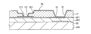
上記のマスク10を用いて製造された、本発明の実施例によるTFTパネル100の(画素マトリクスの列方向に沿った)断面を図3に示す。図3に示されているように、TFTパネル100は、基板110、ストレージ電極120、第1誘電膜130、信号出力ユニット(図3には示されていない)、誘電パターン150、絶縁パターン160、及び画素電極170を含む。尚、図3には信号出力ユニットの出力端140が示されている。
FIG. 3 shows a cross section (along the column direction of the pixel matrix) of the
基板110は透明基板(好ましくはガラス基板)である。ストレージ電極120は好ましくは、基板110の上に形成された複数の線状電極であり、それぞれが画素マトリクスの行方向(以下、第1方向という)に延び、各行のサブピクセルと交差している(図5に示されている破線参照)。ストレージ電極120は一定の電位に維持される。図4に示されているように、ストレージ電極120は好ましくはモリブデンパターン122及びアルミニウムパターン124の積層構造を含む。更に好ましくは、アルミニウムパターン124がモリブデンパターン122の上に配置されている。その他に、ストレージ電極120がアルミニウムパターン又はアルミニウム合金パターンを含んでいても良い。第1誘電膜130は基板110とストレージ電極120とを覆い、ストレージ電極120をその上部の膜(特に画素電極170)から絶縁する。第1誘電膜130は好ましくはシリコン窒化物(SiNX)を含み、更に好ましくは化学気相蒸着(CVD)によって形成される。
The
図5に示されているように、信号出力ユニット125は、ゲートラインGL、データラインDL、チャンネルパターンCP、及び出力端(すなわち、薄膜トランジスタのドレイン電極)140を含む。ゲートラインGLは基板110と第1誘電膜130との間に挟まれた複数の線状電極であり、それぞれが画素マトリクスの各行間を第1方向に延びている。各ゲートラインGLは複数個のゲート電極GEを含む。ゲート電極GEは各サブピクセルに一つずつ設けられ、ゲートラインGLから画素マトリクスの列方向(以下、第2方向という)に突出している。例えば表示装置の解像度が1024×768であり、かつ各画素が行方向に並んだ3個のサブピクセルを含む場合、ゲートラインGLは約768本であり、ゲート電極GEは約1024×3個である。ゲートラインGLは好ましくは、モリブデンパターン及びアルミニウムパターンを含む。ゲートラインGL及びストレージ電極120は好ましくは同時に形成される。
As shown in FIG. 5, the
データラインDLは第1誘電膜130の上に形成された複数の線状電極であり、それぞれが画素マトリクスの各列間を第2方向に延びている(図5参照)。各データラインDLは複数個のソース電極SEを含む。ソース電極SEは各サブピクセルに一つずつ設けられ、データラインDLから第1方向に突出している。例えば表示装置の解像度が1024×768であり、かつ各画素が行方向に並んだ3個のサブピクセルを含む場合、データラインDLは約1024×3本であり、ソース電極SEは約768個である。データラインDLは、好ましくは、第1モリブデンパターン、アルミニウムパターン、及び第2モリブデンパターンを含む。更に好ましくは、第1モリブデンパターンの上にアルミニウムパターンが形成され、アルミニウムパターンの上に第2モリブデンパターンが形成されている。
The data line DL is a plurality of linear electrodes formed on the
チャンネルパターンCPは半導体のパターンであり、特にゲート電極GEを覆う第1誘電膜130の各領域の上に配置されている。チャンネルパターンCPは好ましくは後述のようにデータラインDL及び信号出力ユニットの出力端(ドレイン電極)140と同時にパターニングされるので、チャンネルパターンCPはデータラインDL及びドレイン電極140の各下地にも配置されている(図3に示されている二点鎖線部B、及び図6参照)。チャンネルパターンCPは好ましくは、アモルファスシリコンパターンCP1、及びその上に配置された高濃度イオンドーピングアモルファスシリコンパターンCP2を含む。チャンネルパターンCPの一部の上にはソース電極SEが重なって電気的に連結されている。
The channel pattern CP is a semiconductor pattern, and is disposed on each region of the
ドレイン電極140は各サブピクセルに一つずつ、第1誘電膜130の上に形成されている(図3参照)。ドレイン電極140の一部はチャンネルパターンCPの上に重なって電気的に連結されている(図6参照)。図6に示されているように、ドレイン電極140は好ましくは、第1モリブデンパターンMP1、アルミニウムパターンAP、及び第2モリブデンパターンMP2を含む。更に好ましくは、第1モリブデンパターンMP1の上にアルミニウムパターンAPが形成され、アルミニウムパターンAPの上に第2モリブデンパターンMP2が形成されている。
The
ゲート電極GE、それを覆う第1誘電膜130の部分、チャンネルパターンCP、ソース電極SE、及びドレイン電極140がTFT(特にMOSFET)を構成している(図5参照)。ゲートラインGLに対して外部からタイミング信号が印加されたとき、ゲート電極GEの電圧が変動し、ゲート電極GEを覆うチャンネルパターンCPの部分にチャンネルが形成される。すなわち、上記のTFTがターンオンする。そのとき、データラインDLに対して外部から印加されたデータ信号が、チャンネルパターンCPに形成されたチャンネルを通してドレイン電極140に伝達される。
The gate electrode GE, the portion of the
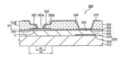
図3に示されているように、誘電パターン150が第1誘電膜130を覆い、更に絶縁パターン160が誘電パターン150を覆っている。それにより、信号出力ユニットが外部から絶縁されている。誘電パターン150は好ましくはシリコン窒化物を含み、その厚みが好ましくは約0.2μm〜0.6μmであり、更に好ましくは0.5μmである。ドレイン電極140を覆う誘電パターン150の部分には開口部152が形成され、その上を覆う絶縁パターン160の部分には第1開口部162aと第2開口部162bとが形成され、併せて第1コンタクトホールを構成している。第1コンタクトホールからはドレイン電極140の一部が露出している。好ましくは、絶縁パターン160の第1開口部162aのサイズA1は第2開口部162bのサイズA2より小さい。第1開口部162aの高さH1は好ましくは絶縁膜ILの最大厚と実質的に等しく、第2開口部162bの高さH2は好ましくは絶縁パターン160の最大厚H1の半分程度である。例えば、絶縁パターン160の最大厚H1(すなわち、第1開口部162aの高さ)が約1.7μm〜3.0μmである場合、第2開口部162bの高さH2は約1.35μm〜1.5μmである。一方、ストレージ電極120の領域を覆う絶縁パターン160の部分には第3開口部164が形成され、第2コンタクトホールを構成している。第2コンタクトホール164からは、ストレージ電極120の上方を覆う誘電パターン150の部分が露出している。
As shown in FIG. 3, the
画素電極170は各サブピクセルに一つずつ設けられ、各サブピクセルのほぼ全体を覆っている(図5参照)。画素電極170は特に、第1コンタクトホール152、162a、162bの内側と第2コンタクトホール164の内側とを覆っている(図3参照)。画素電極170は好ましくは透明な導電性物質から成り、更に好ましくは、酸化亜鉛インジウム(IZO)、酸化スズインジウム(ITO)、または、アモルファス酸化スズインジウム(a−ITO)を含む。画素電極170の一部は第1コンタクトホール152、162a、162bを通じてドレイン電極140に電気的に連結されている。図5に示されているTFTがターンオンするとき、データラインDLからチャンネルパターンCPを通してドレイン電極140に伝達されたデータ信号が、第1コンタクトホール152、162a、162bを通じて画素電極170に伝達される。
One
画素電極170の別の一部172は第2コンタクトホール164の内部で、誘電パターン150と第1誘電膜130とを隔ててストレージ電極120と向かい合っている(図3参照)。ここで、第2コンタクトホール164はストレージ電極120より広くても狭くても良い。以下、ストレージ電極120と向かい合っている画素電極170の部分172をストレージ電極部という。ストレージ電極部172とストレージ電極120との間の静電容量がストレージキャパシタとして利用される。図5に示されているTFTがターンオンするとき、データラインDLから画素電極170に対して印加されるデータ信号により、ストレージキャパシタが充電される。ここで、第2コンタクトホール164の内側ではストレージ電極120とストレージ電極部172との間隔が狭いので、ストレージキャパシタの容量は十分に大きい。従って、上記のTFTがターンオフした後も、ストレージキャパシタは一フレームの間、画素電極170の電圧(画素電圧)を安定に維持する。
Another
図3に示されているTFTパネル100は好ましくは、以下の工程で形成される。
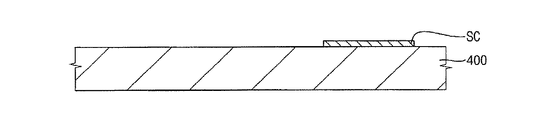
最初の工程では、ゲートラインGLとストレージ電極120とを基板110の上に、以下の順でパターニングする(図7、8参照)。まず、透明な基板(好ましくはガラス基板)200の全面に金属層(図示せず)が形成される。その金属層は好ましくは、モリブデン薄膜及びその上に積層されたアルミニウム薄膜を含む。次に、その金属層の上にフォトレジストが重ねられ、フォトリソグラフィによってパターニングされる。それにより得られたフォトレジストパターンをマスクとして利用し、金属層をエッチングによってパターニングする。その結果、基板200にはストレージ電極SCがゲートラインGLと共に形成される。ストレージ電極SCとゲートラインGLとは、第1方向では平行に延び、第2方向では交互に配置されている。各ゲートラインGLにはゲート電極GEが形成され、各ストレージ電極SCには拡張部EPが形成される。これらの拡張部EPが一つずつ各画素電極170(図3参照)と対向し、各ストレージキャパシタの容量を増加させる。
The
In the first step, the gate line GL and the
第二の工程では、データラインDL、ドレイン電極140、及びチャンネルパターンCPを基板110の上に、以下の順で形成する(図9、10参照)。
まず、第1誘電膜FDが基板200の全面に形成される(図10参照)。第1誘電膜FDは好ましくはスピンコーティングまたはスリットコーティングによって形成される。第1誘電膜FDの上には半導体膜が形成される。半導体膜は好ましくは、アモルファスシリコン薄膜及び高濃度イオンドーピングアモルファスシリコン薄膜を含む。更に好ましくは、高濃度イオンドーピングアモルファスシリコン薄膜がアモルファスシリコン薄膜の上に形成される。高濃度イオンドーピングアモルファスシリコン薄膜の上にはソース/ドレイン金属層(図示せず)が形成される。ソース/ドレイン金属層は好ましくは、第1モリブデン薄膜、アルミニウム薄膜、及び第2モリブデン薄膜を含む。更に好ましくは、アルミニウム薄膜が第1モリブデン薄膜の上に形成され、第2モリブデン薄膜がアルミニウム薄膜の上に形成される。
In the second step, the data line DL, the
First, the first dielectric film FD is formed on the entire surface of the substrate 200 (see FIG. 10). The first dielectric film FD is preferably formed by spin coating or slit coating. A semiconductor film is formed on the first dielectric film FD. The semiconductor film preferably includes an amorphous silicon thin film and a highly ion-doped amorphous silicon thin film. More preferably, a high concentration ion-doped amorphous silicon thin film is formed on the amorphous silicon thin film. A source / drain metal layer (not shown) is formed on the high-concentration ion-doped amorphous silicon thin film. The source / drain metal layer preferably includes a first molybdenum thin film, an aluminum thin film, and a second molybdenum thin film. More preferably, the aluminum thin film is formed on the first molybdenum thin film, and the second molybdenum thin film is formed on the aluminum thin film.
次に、ソース/ドレイン金属層の上にフォトレジスト薄膜が形成され、好ましくはハーフトーン露光を採用したフォトリソグラフィによってパターニングされる。それにより得られたフォトレジストパターンのうち、特に、ソース電極とドレイン電極との隙間になるべき領域を覆う部分が十分に薄く形成される。そのようなフォトレジストパターンをマスクとして利用し、半導体膜とソース/ドレイン金属層とを同時にエッチングによってパターニングし、データラインDLを形成する(図9参照)。各データラインDLには突出部SE/DEが形成される。突出部SE/DEはデータラインDLからゲート電極GEの上方を越えて第1方向に延びている。好ましくはアッシングにより上記のフォトレジストパターンの薄い部分を除去してその下地の突出部SE/DEを露出させる。その後、残りのフォトレジストパターンをマスクとして利用し、突出部SE/DEの露出部分とその下地の高濃度イオンドーピングアモルファスシリコン薄膜CP2(図6参照)とをエッチングにより除去する。こうして、ソース電極SEとドレイン電極DEとが分離され、それらの間からチャンネルパターンCPの一部(特にアモルファスシリコン薄膜CP1(図6参照))が露出する。チャンネルパターンCPのその露出部分からは高濃度イオンドーピングアモルファスシリコン薄膜CP2(図9参照)が除去されているので、ソース電極SE及びドレイン電極DEが電気的にも分離される。 Next, a photoresist thin film is formed on the source / drain metal layer and is preferably patterned by photolithography employing halftone exposure. Of the photoresist pattern obtained thereby, in particular, a portion covering a region to be a gap between the source electrode and the drain electrode is formed sufficiently thin. Using such a photoresist pattern as a mask, the semiconductor film and the source / drain metal layer are simultaneously patterned by etching to form the data line DL (see FIG. 9). A protrusion SE / DE is formed in each data line DL. The protrusion SE / DE extends in the first direction from the data line DL over the gate electrode GE. Preferably, the thin portion of the photoresist pattern is removed by ashing to expose the underlying protrusion SE / DE. Thereafter, the remaining photoresist pattern is used as a mask, and the exposed portion of the protrusion SE / DE and the underlying high-concentration ion-doped amorphous silicon thin film CP2 (see FIG. 6) are removed by etching. Thus, the source electrode SE and the drain electrode DE are separated, and a part of the channel pattern CP (particularly the amorphous silicon thin film CP1 (see FIG. 6)) is exposed from between them. Since the high-concentration ion-doped amorphous silicon thin film CP2 (see FIG. 9) is removed from the exposed portion of the channel pattern CP, the source electrode SE and the drain electrode DE are also electrically separated.
第三の工程では、第2誘電膜及び絶縁膜を以下の順で形成する(図11参照)。まず、第1誘電膜FDの上に第2誘電膜SDが形成される。第2誘電膜SDは好ましくはシリコン窒化物を含む。第2誘電膜SDは特にドレイン電極DEを覆う。次に、第2誘電膜SDの上に絶縁膜ILが形成される。絶縁膜ILは特に感光物質を含む。 In the third step, the second dielectric film and the insulating film are formed in the following order (see FIG. 11). First, the second dielectric film SD is formed on the first dielectric film FD. The second dielectric film SD preferably contains silicon nitride. The second dielectric film SD particularly covers the drain electrode DE. Next, the insulating film IL is formed on the second dielectric film SD. The insulating film IL particularly contains a photosensitive material.
第四の工程では、図1、2に示されているマスク10を用い、絶縁膜ILを以下の順でパターニングする(図12、13参照)。まず、図12に示されているように、絶縁膜ILが形成された基板200の上方にマスク10が配置される。特にマスク10の位置が精密に調節され、第1露光部14がドレイン電極DEの上方に配置され、第2露光部16がストレージ電極SCの上方に配置される。次に、絶縁膜ILがマスク10の第1露光部14及び第2露光部16を通過した光に曝されて各露光部分が感光する。第1光透過部14aに対向する絶縁膜ILの第1部分IL1は第1光量で露光されるので、その全体が感光する。第2光透過部14bに対向する絶縁膜ILの第2部分IL2は第2光量で露光されるので、第1部分IL1より薄い(好ましくは第1部分IL1の半分程度の厚さの)部分が感光する。第3光透過部16aに対向する絶縁膜ILの第3部分IL3は第3光量で露光されるので、第1部分IL1よりは薄く、第2部分IL2よりは厚い部分が感光する。
In the fourth step, the insulating film IL is patterned in the following order using the
図12に示されている露光工程により感光された絶縁膜ILの各部分を現像工程で除去する。それにより、図13に示されているように、第2誘電膜SDの上に絶縁パターンIPが形成される。絶縁パターンIPでは、第1部分IL1のほぼ全体が除去されて第1開口部FCが形成され、第2部分IL2がほぼ半分の厚みまで除去されて第2開口部SC1が形成される。更に、第3部分IL3が一部Lを薄く残して除去され、第3開口部TCが形成される。第2開口部SC1は第1開口部FCより広い。第1開口部FCの高さH1は絶縁膜ILの最大厚と実質的に等しく、第2開口部SC1の高さH2は絶縁膜ILの最大厚H1の半分程度である。第3開口部TCの内側に残留している絶縁膜ILの一部Lの厚みTは好ましくは第2誘電膜SDの厚みと実質的に等しい。その残留部分Lが、ストレージ電極SCの上方を覆っている第2誘電膜SDの部分を、意図しないエッチングから保護する。それにより、ストレージキャパシタの容量を更に正確に制御できるので、フリッカや残像等の画質不良を更に低減できる。尚、第3開口部TCの周辺に、第4開口部FC1を更に形成しても良い(図13に示されている破線部参照)。第4開口部FC1は第3開口部TCより広く、その高さが絶縁膜ILの最大厚より小さい。 Each part of the insulating film IL exposed by the exposure process shown in FIG. 12 is removed in the development process. Thereby, as shown in FIG. 13, an insulating pattern IP is formed on the second dielectric film SD. In the insulating pattern IP, almost the entire first portion IL1 is removed to form the first opening FC, and the second portion IL2 is removed to almost half the thickness to form the second opening SC1. Further, the third portion IL3 is removed leaving a part L thin, and the third opening TC is formed. The second opening SC1 is wider than the first opening FC. The height H1 of the first opening FC is substantially equal to the maximum thickness of the insulating film IL, and the height H2 of the second opening SC1 is about half of the maximum thickness H1 of the insulating film IL. The thickness T of the part L of the insulating film IL remaining inside the third opening TC is preferably substantially equal to the thickness of the second dielectric film SD. The remaining portion L protects the portion of the second dielectric film SD covering the storage electrode SC from unintentional etching. As a result, the capacity of the storage capacitor can be controlled more accurately, and image quality defects such as flicker and afterimage can be further reduced. A fourth opening FC1 may be further formed around the third opening TC (see the broken line portion shown in FIG. 13). The fourth opening FC1 is wider than the third opening TC and its height is smaller than the maximum thickness of the insulating film IL.
第五の工程では、図13に示されている絶縁パターンIPと第2誘電膜SDとを以下の順でパターニングし、図14に示されている誘電パターンDPを形成する。まず、絶縁パターンIP及び第2誘電膜SDに対してドライエッチング又はウェットエッチングを行う。そのとき、絶縁パターンIPの第1開口部FCの内側から第2誘電膜SDの露出部分が除去される。それにより、誘電パターンDPに開口部CT1が形成される(図14参照)。絶縁パターンIPの第1開口部FCと第2開口部SC1、及び誘電パターンDPの開口部CT1が第1コンタクトホールを構成する。第1コンタクトホールCT1、FC、SC1からはドレイン電極DEの一部が露出する。一方、第3開口部TCの内側では、絶縁パターンIPの残留部分Lが、ストレージ電極SCの上方を覆っている第2誘電膜SDの部分をエッチングから保護する(図13参照)。次に、O2プラズマを利用したアッシングにより、第3開口部TCの内側から絶縁パターンIPの残留部分Lを除去し、絶縁パターンIPに第2コンタクトホールCT2を形成する(図14参照)。第2コンタクトホールCT2からは、ストレージ電極SCの上方を覆っている誘電パターンDPの部分が露出する。尚、第3開口部TCの周辺に上記の第4開口部FC1(図13参照)を更に形成することで、第2コンタクトホールCT2の内壁が階段状であっても良い(図14に示されている破線部参照)。その段差は、第1コンタクトホールCT1、FC、SC1の内壁の段差と同様に、コンタクトホールからの光漏れを低減させる。 In the fifth step, the insulating pattern IP and the second dielectric film SD shown in FIG. 13 are patterned in the following order to form the dielectric pattern DP shown in FIG. First, dry etching or wet etching is performed on the insulating pattern IP and the second dielectric film SD. At that time, the exposed portion of the second dielectric film SD is removed from the inside of the first opening FC of the insulating pattern IP. Thereby, an opening CT1 is formed in the dielectric pattern DP (see FIG. 14). The first opening FC and the second opening SC1 of the insulating pattern IP and the opening CT1 of the dielectric pattern DP constitute a first contact hole. A part of the drain electrode DE is exposed from the first contact holes CT1, FC, SC1. On the other hand, inside the third opening TC, the remaining portion L of the insulating pattern IP protects the portion of the second dielectric film SD covering the storage electrode SC from etching (see FIG. 13). Next, the remaining portion L of the insulating pattern IP is removed from the inside of the third opening TC by ashing using O 2 plasma, and the second contact hole CT2 is formed in the insulating pattern IP (see FIG. 14). From the second contact hole CT2, a portion of the dielectric pattern DP covering the storage electrode SC is exposed. Incidentally, by further forming the fourth opening FC1 (see FIG. 13) around the third opening TC, the inner wall of the second contact hole CT2 may be stepped (shown in FIG. 14). (See the dashed line). The step reduces light leakage from the contact hole, similar to the step on the inner wall of the first contact holes CT1, FC, SC1.
第六の工程では、図14に示されている絶縁パターンIPの上に、図15に示されている画素電極PEを以下の順で形成する。まず、絶縁パターンIPの全面に導電性透明薄膜(図示せず)が形成され、その導電性透明薄膜の上にフォトレジスト薄膜が形成される。次に、フォトレジスト薄膜がパターニングされ、導電性透明薄膜の上にフォトレジストパターンが形成される。続いて、そのフォトレジストパターンをマスクとして利用して導電性透明薄膜をドライエッチング又はウェットエッチングでパターニングし、画素電極PEを形成する(図15参照)。画素電極PEの一部が第1コンタクトホールCT1、FC、SC1を通じてドレイン電極DEと電気的に連結される。それにより、画素電極PEに対してドレイン電極DEを通じて画素電圧が印加される。更に、画素電極PEの他の一部が第2コンタクトホールCT2を通じて誘電パターンDPに接触し、誘電パターンDPと第1誘電膜FDとを隔ててストレージ電極SCと向かい合う。こうして、画素電極PEのその部分(ストレージ電極部)とストレージ電極SCとが第1誘電膜FD及び誘電パターンDPを挟み、ストレージキャパシタを構成する。 In the sixth step, the pixel electrode PE shown in FIG. 15 is formed in the following order on the insulating pattern IP shown in FIG. First, a conductive transparent thin film (not shown) is formed on the entire surface of the insulating pattern IP, and a photoresist thin film is formed on the conductive transparent thin film. Next, the photoresist thin film is patterned to form a photoresist pattern on the conductive transparent thin film. Subsequently, using the photoresist pattern as a mask, the conductive transparent thin film is patterned by dry etching or wet etching to form a pixel electrode PE (see FIG. 15). A part of the pixel electrode PE is electrically connected to the drain electrode DE through the first contact holes CT1, FC, SC1. Thereby, a pixel voltage is applied to the pixel electrode PE through the drain electrode DE. Furthermore, the other part of the pixel electrode PE contacts the dielectric pattern DP through the second contact hole CT2, and faces the storage electrode SC with the dielectric pattern DP and the first dielectric film FD interposed therebetween. Thus, the portion (storage electrode portion) of the pixel electrode PE and the storage electrode SC sandwich the first dielectric film FD and the dielectric pattern DP to constitute a storage capacitor.
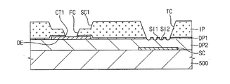
本発明の別の実施例によるTFTパネル300の(特に画素マトリクスの列方向での)断面を図16に示す。図16に示されているように、TFTパネル300は、基板310、ストレージ電極320、第1誘電膜330、信号出力ユニット325(図17参照)、誘電パターン350、絶縁パターン360、及び画素電極370を含む。尚、図16には、信号出力ユニットの出力端(すなわち、薄膜トランジスタのドレイン電極)340が示されている。図16〜18に示されているTFTパネル300の各構成要素は、ストレージ電極320の上方を覆っている第1誘電膜330、誘電パターン350、及び画素電極370の各部分の形状を除き、図3〜6に示されているTFTパネル100の各構成要素と同様である。従って、それら同様な構成要素の詳細については、図3〜6に示されているTFTパネル100についての説明を援用する。
FIG. 16 shows a cross section (particularly in the column direction of the pixel matrix) of a
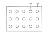
第2コンタクトホール364は、ストレージ電極320の上方に形成されている(図16参照)。第2コンタクトホール364の内側では画素電極370が誘電パターン350の露出部分を直に覆っている。図16に示されているTFTパネル300では図3に示されているTFTパネル100とは異なり、第2コンタクトホール364の内側を覆っている誘電パターン350と画素電極370の部分とに、表面積増加部355が形成されている。表面積増加部355は細かい凹凸であり、好ましくは、図19に示されている通り、第2コンタクトホール364の内側を覆っている誘電パターン350(及び画素電極370)の表面に形成された複数の窪みのマトリクスである。その他に、表面積増加部355が、誘電パターン350(及び画素電極370)の表面に形成された突起であっても良い。表面積増加部355で、突起と窪みとが交互に連なり、連続した波形状を形成していても良い。表面積増加部355の凹凸の平面形状は、マスク10の第3光透過部16aのスリットの形状で決まる。例えばマスク10の第3光透過部16aのスリットが図1に示されているような複数の帯状である場合、表面積増加部が、図20に示されているような複数のグルーブ357であり、特に、各グルーブ357が棒形状である。スリットの形状によっては、複数のグルーブを交差させて格子を形成させることもできる。第2コンタクトホール364の内側では、表面積増加部355、357により、誘電パターン350と画素電極370との各表面積が大きい。それにより、ストレージキャパシタの容量が更に大きい。従って、ストレージキャパシタが一フレームの間、画素電圧を更に安定化させる。
The
図16に示されているTFTパネル300は好ましくは、図3に示されているTFTパネル100の形成工程(図7〜15参照)と同様な工程で形成される(図21〜28参照)。
最初の工程ではゲートラインGLとストレージ電極SCとを基板200の上にパターニングする(図21、22参照)。この工程は図7、8に示されている工程と同様であるので、その詳細については図7、8に示されている工程についての上記の説明を援用する。第二の工程では、データラインDL、ドレイン電極DE、及びチャンネルパターンCPを基板の上にパターニングする(図23、24参照)。この工程は図9、10に示されている工程と同様であるので、その詳細については図9、10に示されている工程についての上記の説明を援用する。第三の工程では第2誘電膜SD及び絶縁膜ILを形成する(図25参照)。この工程は図11に示されている工程と同様であるので、その詳細については図11に示されている工程についての上記の説明を援用する。
The
In the first step, the gate line GL and the storage electrode SC are patterned on the substrate 200 (see FIGS. 21 and 22). Since this process is the same as the process shown in FIGS. 7 and 8, the above description of the process shown in FIGS. In the second step, the data line DL, the drain electrode DE, and the channel pattern CP are patterned on the substrate (see FIGS. 23 and 24). Since this process is the same as the process shown in FIGS. 9 and 10, the above description of the process shown in FIGS. In the third step, the second dielectric film SD and the insulating film IL are formed (see FIG. 25). Since this process is the same as the process shown in FIG. 11, the above description of the process shown in FIG.
第四の工程では、図1、2に示されているマスクと同様なマスク10を用い、絶縁膜ILをパターニングして絶縁パターンIPを形成する(図25、26参照)。尚、ドレイン電極DEを覆っている絶縁膜ILの部分のパターニングは、図12、13に示されている工程でのパターニングと同様であるので、その詳細については、図12、13に示されている工程についての上記の説明を援用する。
In the fourth step, an insulating pattern IP is formed by patterning the insulating film IL using a
第2露光部16の第3光透過部16aに対向する絶縁膜ILの第3部分IL3は第3光量で露光されるので、第1部分IL1よりは薄く、第2部分IL2よりは厚い部分が感光する。従って、第3開口部TCの内側には、図26に示されているような絶縁膜ILの薄い部分Lが残る。その残留部分Lの厚みは好ましくは、第2誘電膜SDの厚みと実質的に等しい。その残留部分Lが図13に示されている残留部分Lと同様に、ストレージ電極SCの上方を覆っている第2誘電膜SDの部分を、第1開口部FCを形成するためのエッチングの間、保護する。更に、図25に示されているマスク10の第3光透過部16aは、図1に示されているものとはスリットの形状、幅、若しくは間隔、または絶縁膜ILからの距離が異なる。その他に、光源の波長や光量、または露光時間が異なっていても良い。それにより、第3光透過部16aに対向する絶縁膜ILの第3部分IL3では第3光量が、第3光透過部16aのスリットの形状に応じて場所ごとに変化する(図25に示されている破線R2参照)。その結果、絶縁膜ILの感光部分の厚みが規則的に、かつ比較的大きく変化するので、図26に示されている第3開口部TCの内側の残留部分Lの上面には、図13に示されているものとは異なり、凸パターンCCが形成される。凸パターンCCは好ましくは、残留部分Lの上面から隆起した棒形状又は格子形状の凸部である。
Since the third portion IL3 of the insulating film IL facing the third
第五の工程では、図26に示されている絶縁パターンIPと第2誘電膜SDとをパターニングし、図27に示されている誘電パターンDPを形成する。尚、図27に示されている絶縁パターンIPの第1開口部FCと第2開口部SC1とのパターニング、及び誘電パターンDPの開口部CT1のパターニングは、図13、14に示されている工程でのパターニングと同様であるので、その詳細については図13、14に示されている工程についての上記の説明を援用する。 In the fifth step, the insulating pattern IP and the second dielectric film SD shown in FIG. 26 are patterned to form the dielectric pattern DP shown in FIG. The patterning of the first opening FC and the second opening SC1 of the insulating pattern IP and the patterning of the opening CT1 of the dielectric pattern DP shown in FIG. 27 are the steps shown in FIGS. Since the patterning is similar to the patterning in FIG. 13, the above description of the steps shown in FIGS.
絶縁パターンIPの第3開口部TCの内側では、絶縁パターンIPの残留部分Lとその下地の第2誘電膜SDとがドライエッチング又はウェットエッチングでパターニングされる(図27参照)。ここで、凸パターンCC以外では絶縁パターンIPの残留部分Lが除去され、その下地の第2誘電膜SDの表面が削られる。一方、凸パターンCCでは絶縁パターンIPの残留部分Lが厚く、完全には除去されないので、その下地の第2誘電膜SDの表面が削られない。こうして、ストレージ電極SCの上方を覆っている第2誘電膜SDの表面に、図19または図20に示されているような平面形状の複数の窪みまたはグルーブ、すなわち表面積増加部SIが形成される。その後、絶縁パターンIPの凸パターンCCが好ましくはアッシングによって除去される。こうして、絶縁パターンIPの第3開口部TCが第2コンタクトホールとして構成される。尚、図27とは異なり、第2コンタクトホール(絶縁パターンIPの第3開口部)TCの内壁が第1コンタクトホール(第1開口部FCと第2開口部SC1)の内壁と同様に階段状であっても良い。 Inside the third opening TC of the insulating pattern IP, the remaining portion L of the insulating pattern IP and the underlying second dielectric film SD are patterned by dry etching or wet etching (see FIG. 27). Here, except for the convex pattern CC, the remaining portion L of the insulating pattern IP is removed, and the surface of the underlying second dielectric film SD is shaved. On the other hand, in the convex pattern CC, the remaining portion L of the insulating pattern IP is thick and is not completely removed, so that the surface of the underlying second dielectric film SD is not scraped. Thus, a plurality of planar recesses or grooves, that is, a surface area increasing portion SI as shown in FIG. 19 or FIG. 20, is formed on the surface of the second dielectric film SD covering the storage electrode SC. . Thereafter, the convex pattern CC of the insulating pattern IP is preferably removed by ashing. Thus, the third opening TC of the insulating pattern IP is configured as the second contact hole. Unlike FIG. 27, the inner wall of the second contact hole (third opening of the insulating pattern IP) TC is stepped like the inner wall of the first contact hole (first opening FC and second opening SC1). It may be.
第六の工程では、図27に示されている絶縁パターンIPの上に、図28に示されている画素電極PEを形成する。この工程は図15に示されている工程と同様であるので、その詳細については図15に示されている工程についての上記の説明を援用する。但し、図28では図15とは異なり、第2コンタクトホールTCを通じて誘電パターンDPの表面に接触する画素電極PEの部分に、誘電パターンDPの表面と同様な凹凸形状、すなわち表面積増加部SIが形成される。 In the sixth step, the pixel electrode PE shown in FIG. 28 is formed on the insulating pattern IP shown in FIG. Since this process is the same as the process shown in FIG. 15, the above description of the process shown in FIG. However, unlike FIG. 15, in FIG. 28, the same uneven shape as the surface of the dielectric pattern DP, that is, the surface area increasing portion SI is formed in the portion of the pixel electrode PE that contacts the surface of the dielectric pattern DP through the second contact hole TC. Is done.
第2コンタクトホールの内側では、図16とは異なり、誘電パターンの表面に窪みではなく貫通穴が形成され、更にその下の第1誘電膜の表面に窪みが形成されても良い。そのようなTFTパネルは好ましくは、図21〜28に示されている工程に代え、図29〜36に示されている工程で製造される。尚、図29〜36に示されている構成要素及び工程のうち、図21〜28に示されている構成要素及び工程と同様なものについては、図21〜28についての説明を援用する。 Unlike FIG. 16, inside the second contact hole, a through hole may be formed on the surface of the dielectric pattern instead of a recess, and a recess may be formed on the surface of the first dielectric film therebelow. Such a TFT panel is preferably manufactured by the process shown in FIGS. 29 to 36 instead of the process shown in FIGS. In addition, about the thing similar to the component and process shown by FIGS. 21-28 among the components and processes shown by FIGS. 29-36, description about FIGS. 21-28 is used.
図35に示されている第五の工程では、図27に示されている第五の工程と同様に、図34に示されている絶縁パターンIPと第2誘電膜SDとをパターニングして第1誘電パターンDP1を形成する。特に、絶縁パターンIPの第3開口部TCの内側では、絶縁パターンIPの残留部分Lとその下地の第2誘電膜SDとがドライエッチング又はウェットエッチングでパターニングされ、第2コンタクトホールが形成される。ここで、図34に示されている凸パターンCC以外では絶縁パターンIPの残留部分Lとその下地の第2誘電膜SDの一部とが共に除去され、第1誘電膜FDの表面が露出する。一方、凸パターンCCでは絶縁パターンIPの残留部分Lが厚いので、特にその下地の第2誘電膜SDの一部、すなわち第1表面積増加部SI1が残る。こうして、第2誘電膜SDから第1誘電パターンDP1が形成される。 In the fifth step shown in FIG. 35, similarly to the fifth step shown in FIG. 27, the insulating pattern IP and the second dielectric film SD shown in FIG. One dielectric pattern DP1 is formed. In particular, inside the third opening TC of the insulating pattern IP, the remaining portion L of the insulating pattern IP and the underlying second dielectric film SD are patterned by dry etching or wet etching to form a second contact hole. . Here, except for the convex pattern CC shown in FIG. 34, the remaining portion L of the insulating pattern IP and a part of the second dielectric film SD underlying the same are removed, and the surface of the first dielectric film FD is exposed. . On the other hand, since the remaining portion L of the insulating pattern IP is thick in the convex pattern CC, a part of the underlying second dielectric film SD, that is, the first surface area increasing portion SI1 remains. Thus, the first dielectric pattern DP1 is formed from the second dielectric film SD.
図35に示されている第五の工程では、図27に示されている第五の工程とは異なり、絶縁パターンIPの凸パターンCCと第1誘電パターンDP1の第1表面積増加部SI1とをマスクとして利用し、第1誘電パターンDP1の間から露出している第1誘電膜FDの表面をパターニングして第2誘電パターンDP2を形成する。特に、第1表面積増加部SI1の間から露出した第2誘電パターンDP2の表面には、図19または図20に示されている平面形状と同様な平面形状の複数の窪みまたはグルーブ、すなわち第2表面積増加部SI2が形成される。その後、第1表面積増加部S11の上に残留している絶縁パターンIP、すなわち凸パターンCC(図34参照)が好ましくはドライエッチングまたはアッシングによって除去される。 In the fifth step shown in FIG. 35, unlike the fifth step shown in FIG. 27, the convex pattern CC of the insulating pattern IP and the first surface area increasing portion SI1 of the first dielectric pattern DP1 are provided. Using the mask as a mask, the surface of the first dielectric film FD exposed from between the first dielectric patterns DP1 is patterned to form a second dielectric pattern DP2. In particular, the surface of the second dielectric pattern DP2 exposed from between the first surface area increasing portions SI1 has a plurality of recesses or grooves having a planar shape similar to the planar shape shown in FIG. A surface area increasing portion SI2 is formed. Thereafter, the insulating pattern IP remaining on the first surface area increasing portion S11, that is, the convex pattern CC (see FIG. 34) is preferably removed by dry etching or ashing.
第六の工程では、図35に示されている絶縁パターンIPの上に、図36に示されている画素電極PEを形成する。この工程は図28に示されている工程と同様であるので、その詳細については図28に示されている工程についての説明を援用する。特に、図36では図28と同様に、第2コンタクトホールTCを通じて第2誘電パターンDP2の表面に接触する画素電極PEの部分に、第2誘電パターンDP2の表面と同様な窪み、すなわち表面積増加部SIが形成される。 In the sixth step, the pixel electrode PE shown in FIG. 36 is formed on the insulating pattern IP shown in FIG. Since this process is the same as the process shown in FIG. 28, the description of the process shown in FIG. In particular, in FIG. 36, as in FIG. 28, in the portion of the pixel electrode PE that contacts the surface of the second dielectric pattern DP2 through the second contact hole TC, a depression similar to the surface of the second dielectric pattern DP2, ie, a surface area increasing portion. SI is formed.
本発明の上記の実施例による製造方法では、図1、2に示されているマスク10に代え、図37、38に示されているマスク70が用いられても良い。すなわち、このマスク70は、図38に示されているように、薄膜トランジスタのドレイン電極77h及びストレージ電極77bのそれぞれの上方での絶縁膜77e(フォトレジストフィルム)のパターニングで使用される。
In the manufacturing method according to the above-described embodiment of the present invention, the
図37に示されているように、マスク70は、マスク本体72、スリット露光部74、及び光吸収−透過部76を含む。図38に示されているように、マスク本体72は更に、光透過基板72a、及びその上に形成された光遮断膜72bを含む。絶縁膜77eの露光時にはマスク70の上面が、その上方に配置された光源(図示せず)から第1光量の光R1を受ける。光遮断膜72bはその光R1を吸収する。一方、スリット露光部74及び光吸収−透過部76は、後述のように、光源から照射された光R1を透過させる。光透過基板72aは透明な基板であり、スリット露光部74及び光吸収−透過部76を透過した光を、マスク70の下面から外部に出射する。
As shown in FIG. 37, the
図39に示されているように、スリット露光部74は複数個のスリット74aを含む。各スリット74aは好ましくは、四角形の閉じたループ形状であり、それらが同じ中心を共有している。その他に、スリット74aが平行に並置された直線形状であっても良い。スリット露光部74の中心部には、好ましくは四角形の穴74bが開いている。各スリット74aは光遮断膜72bの一部をパターニングして形成されている。各スリット74aの幅と間隔とは光源の分解能より小さく、好ましくは約1.2μm〜1.4μmであり、更に好ましくは約1.3μmである。一方、スリット露光部74の中心部の穴74bのサイズは各スリット74aの幅より大きく、好ましくは光源の分解能より大きい。図38に示されているように、絶縁膜77eの露光時、スリット露光部74の中心部の穴74bが、ドレイン電極77hを覆う絶縁膜77eの領域78の上方に配置される。スリット露光部74では光源から出射された光R1が回折されるので、穴74bと対向する絶縁膜77eの領域78が第1光量でほぼ一様に露光され、スリット74aと対向する領域79が第2光量(好ましくは第1光量の半分程度)でほぼ一様に露光される。従って、穴74bと対向する絶縁膜77eの領域78ではほぼ全ての部分が感光し、スリット74aと対向する絶縁膜77eの領域79では一部(好ましくは半分程度の厚みの部分)が感光する(図38に示されている絶縁膜77e内の斜線部78、79参照)。
As shown in FIG. 39, the
光吸収−透過部76は光遮断膜72bとは異なる膜で覆われた部分であり、好ましくは酸化クロム薄膜又は窒化クロム薄膜を含む。光吸収−透過部76は特に、光源からマスク70の上面に照射された光R1の一部を透過させ、残りを反射し、又は吸収する。光源から出射される光R1の波長が約193nm〜436nmである場合、光吸収−透過部76は好ましくは、その光R1の約20%〜70%を透過する。ここで、光吸収−透過部76の透過率は光吸収−透過部76の厚みで調節可能である。図38に示されているように、絶縁膜77eの露光時、光吸収−透過部76は、ストレージ電極77bを覆う絶縁膜77eの領域80の上方に配置される。光源からの光R1は光吸収−透過部76の透過で弱められるので、光吸収−透過部76と対向する絶縁膜77eの領域80は第3光量(第1光量より小さく、第2光量より大きい)で一様に露光される。従って、絶縁膜60のその領域80では、感光せずに残留する部分が、スリット74aと対向する絶縁膜77eの領域79に残留する部分より薄く、好ましくは、絶縁膜77eの下に配置された誘電パターン77dと実質的に同じ厚みである(図38に示されている絶縁膜77e内の斜線部80参照)。ここで、光吸収−透過部76から出射される光の輝度は、図1、2に示されている第2露光部16を通過した光の輝度より均一度が高い。従って、光吸収−透過部76と対向する絶縁膜77eの領域80では感光部分の厚みが更に均一化される。それ故、絶縁膜77eを現像した後にその領域80に残留する部分を、アッシングによって誘電パターン77dの上から完全に除去できる。
The light absorbing / transmitting
図37、38に示されている上記のマスク70は好ましくは、以下のようなTFTパネルの製造工程で利用される(図40〜46参照)。ここで、図40〜46に示されている構成要素及び工程のうち、図7〜15に示されている構成要素及び工程と同様なものについては、図7〜15についての説明を援用する。
The above-described
第四の工程では、図37、38に示されているマスク70を用い、図40に示されている、第一〜第三の工程を経た絶縁膜F3を以下の順でパターニングする。まず、図42に示されているように、絶縁膜F3が形成された基板600の上方にマスク70が配置される。特にマスク70の位置が精密に調整され、スリット露光部74が、第2誘電膜F2と絶縁膜F3とで覆われたドレイン電極E3の上方に配置され、光吸収−透過部76が、第1誘電膜F1、第2誘電膜F2、及び絶縁膜F3で覆われたストレージ電極SEPの上方に配置される。次に、図43に示されているように、絶縁膜F3がマスク70のスリット露光部74及び光吸収−透過部76を通過した光R2に曝されて各露光部分が感光する。スリット露光部74の中心部の穴74bと対向する絶縁膜F3の第1領域78は第1光量で露光されるので、その全体が感光し、スリット74aと対向する絶縁膜F3の第2領域79は第2光量で露光されるので、第1領域78より薄い(好ましくは第1領域78の半分程度の厚さの)部分が感光する(図43に示されている絶縁パターンIP1内の斜線部78、79参照)。光吸収−透過部76と対向する絶縁膜F3の第3領域80は第3光量で露光されるので、第1領域78よりは薄く、第2領域79よりは厚い部分が感光する(図43に示されている絶縁パターンIP1内の斜線部80参照)。
In the fourth step, the
図43に示されている露光工程により感光された絶縁膜IP1の各部分を現像工程で除去する。それにより、図44に示されている通り、第2誘電膜F2の上に絶縁パターンIP1が形成される。絶縁パターンIP1には特に、第1開口部FO及び第2開口部SOが形成される。第2開口部SOの内側の絶縁パターンIP1には薄い残留膜Lが形成されている。好ましくはその残留膜Lの厚みが第2誘電膜F2の厚みと実質的に等しい。その残留膜Lが、ストレージ電極SEPの上方を覆っている第2誘電膜F2の部分を、意図しないエッチングから保護する。 Each part of the insulating film IP1 exposed by the exposure process shown in FIG. 43 is removed in the development process. Thereby, as shown in FIG. 44, an insulating pattern IP1 is formed on the second dielectric film F2. In particular, the first opening FO and the second opening SO are formed in the insulating pattern IP1. A thin residual film L is formed on the insulating pattern IP1 inside the second opening SO. Preferably, the thickness of the residual film L is substantially equal to the thickness of the second dielectric film F2. The residual film L protects the portion of the second dielectric film F2 that covers the storage electrode SEP from unintentional etching.
図45に示されている第五の工程は、図14に示されている工程と同様に、図44に示されている絶縁パターンIP1と第2誘電膜F2とを次のようにパターニングして誘電パターンSDPを形成する。まず、第1開口部FOの内側からは第2誘電膜F2の露出部分がドライエッチング又はウェットエッチングで除去され、誘電パターンSDPに開口部T1が形成され、そこからドレイン電極E3の一部が露出する。一方、第2開口部S0の内側では、絶縁パターンIP1の残留膜L(図44参照)が、ストレージ電極SEPの上方を覆っている誘電パターンSDPの部分をエッチングから保護する。次に、アッシングにより、第2開口部S0の内側から絶縁パターンIP1の残留膜Lを除去し、ストレージ電極SEPの上方を覆っている誘電パターンSDPの部分を露出させる。 The fifth step shown in FIG. 45 is similar to the step shown in FIG. 14 except that the insulating pattern IP1 and the second dielectric film F2 shown in FIG. 44 are patterned as follows. A dielectric pattern SDP is formed. First, from the inside of the first opening FO, the exposed portion of the second dielectric film F2 is removed by dry etching or wet etching to form an opening T1 in the dielectric pattern SDP, from which a part of the drain electrode E3 is exposed. To do. On the other hand, inside the second opening S0, the residual film L (see FIG. 44) of the insulating pattern IP1 protects the portion of the dielectric pattern SDP that covers the storage electrode SEP from etching. Next, the residual film L of the insulating pattern IP1 is removed from the inside of the second opening S0 by ashing, and the portion of the dielectric pattern SDP covering the storage electrode SEP is exposed.
図46に示されている第六の工程では、図15に示されている工程と同様に、図45に示されている絶縁パターンIP1の上に透明な画素電極を形成する。尚、その工程の詳細については、図15に示されている工程の説明を援用する。
以上、本発明の実施例について詳細に説明した。しかし、本発明の技術的範囲はそれらの実施例には限定されない。実際、当業者であれば、本発明の思想と精神とから離れることなく、本発明の上記の実施例を修正し、または変更できるだろう。従って、それらの修正や変更も当然に、本発明の技術的範囲に属すると解されるべきである。
In the sixth step shown in FIG. 46, similarly to the step shown in FIG. 15, a transparent pixel electrode is formed on the insulating pattern IP1 shown in FIG. In addition, about the detail of the process, description of the process shown by FIG. 15 is used.
The embodiments of the present invention have been described in detail above. However, the technical scope of the present invention is not limited to these examples. Indeed, those skilled in the art will be able to modify or change the above-described embodiments of the present invention without departing from the spirit and spirit of the invention. Therefore, it should be understood that such modifications and changes belong to the technical scope of the present invention.
10 マスク
12 マスク本体
14 第1露光部
14a 第1光透過部
14b 第2光透過部
16 第2露光部
16a 第3光透過部
20 ストレージ電極
40 ドレイン電極
50 誘電膜
60 絶縁膜
100 薄膜トランジスタパネル
110 基板
120 ストレージ電極
122 モリブデンパターン
124 アルミニウムパターン
125 信号出力ユニット
130 誘電膜
140 ドレイン電極
150 誘電パターン
160 絶縁パターン
170 画素電極
10 Mask
12 Mask body
14 First exposure section
14a First light transmission part
14b Second light transmission part
16 Second exposure section
16a Third light transmission part
20 Storage electrode
40 Drain electrode
50 Dielectric film
60 Insulating film
100 Thin film transistor panel
110 substrates
120 storage electrode
122 Molybdenum pattern
124 aluminum pattern
125 signal output unit
130 Dielectric film
140 Drain electrode
150 Dielectric pattern
160 Insulation pattern
170 pixel electrode
Claims (24)
前記基板と前記ストレージ電極とを第1誘電膜で覆う段階、
半導体膜及び金属層を順に積層し、第2マスクを用いて前記半導体膜及び前記金属層を同時にパターンニングして前記第1誘電膜の上にドレイン電極を形成する段階、
前記ドレイン電極と前記第1誘電膜とを第2誘電膜と絶縁層とで順番に覆う段階、
第3マスクを用いて前記絶縁層をパターニングし、前記ドレイン電極を覆っている領域では前記第2誘電膜を露出させる第2コンタクトホールを形成し、前記ストレージ電極の上方に前記絶縁層の一部を残留させる段階、
前記第2誘電膜の露出部分を除去して前記第2誘電膜の第1コンタクトホールを形成し、そこから前記ドレイン電極を露出させる段階、
前記ストレージ電極の上方から前記絶縁層の残留部分を除去して第3コンタクトホールを形成し、そこから前記第2誘電膜を露出させる段階、及び、
全面を導電性薄膜で覆い、第4マスクを用いて前記導電性薄膜をパターンニングすることで前記絶縁層の上に画素電極を形成し、前記第1コンタクトホールの内側で前記画素電極を前記ドレイン電極と電気的に連結し、前記第3コンタクトホールの内側に前記ストレージ電極と向かい合う前記画素電極のストレージ電極部を形成する段階を含み、
前記ストレージ電極、前記第1誘電膜、前記第2誘電膜、及び前記画素電極の前記ストレージ電極部が互いに重なってストレージキャパシタを構成する表示装置の製造方法。 Forming a storage electrode on the substrate using the first mask;
Covering the substrate and the storage electrode with a first dielectric film;
Stacking a semiconductor film and a metal layer in order, and patterning the semiconductor film and the metal layer simultaneously using a second mask to form a drain electrode on the first dielectric film;
Sequentially covering the drain electrode and the first dielectric film with a second dielectric film and an insulating layer;
The insulating layer is patterned using a third mask, a second contact hole is formed to expose the second dielectric film in a region covering the drain electrode, and a part of the insulating layer is formed above the storage electrode. Leaving the stage,
Removing an exposed portion of the second dielectric film to form a first contact hole of the second dielectric film, and exposing the drain electrode therefrom;
Removing a remaining portion of the insulating layer from above the storage electrode to form a third contact hole, and exposing the second dielectric film therefrom; and
A pixel electrode is formed on the insulating layer by covering the entire surface with a conductive thin film, and patterning the conductive thin film using a fourth mask, and the pixel electrode is placed inside the first contact hole. Forming a storage electrode portion of the pixel electrode that is electrically connected to an electrode and faces the storage electrode inside the third contact hole;
A method of manufacturing a display device, wherein the storage electrode, the first dielectric film, the second dielectric film, and the storage electrode portion of the pixel electrode overlap each other to form a storage capacitor.
前記基板と前記ストレージ電極とを第1誘電膜で覆う段階、
半導体膜及び金属層を順に積層し、第2マスクを用いて前記半導体膜及び前記金属層を同時にパターンニングして前記第1誘電膜の上にドレイン電極を形成する段階、
前記ドレイン電極と前記第1誘電膜とを第2誘電膜と絶縁層とで順番に覆う段階、
第3マスクを用いて前記絶縁層をパターニングし、前記ドレイン電極を覆っている領域では前記第2誘電膜を露出させる第2コンタクトホールを形成し、表面に凹凸パターンを含む前記絶縁層の一部を前記ストレージ電極の上方に残留させる段階、
前記ドレイン電極の上方から前記第2誘電膜の露出部分を除去して前記第2誘電膜の第1コンタクトホールを形成し、そこから前記ドレイン電極を露出させる段階、
前記ストレージ電極の上方から前記絶縁層の残留部分を除去して第3コンタクトホールを形成し、そこから前記第2誘電膜を露出させると共に、その露出した表面に、前記凹凸パターンと同様な形状の表面積増加部を形成する段階、及び、
全面を導電性薄膜で覆い、第4マスクを用いて前記導電性薄膜をパターンニングすることで前記絶縁層の上に画素電極を形成し、前記第1コンタクトホールの内側では前記画素電極を前記ドレイン電極に電気的に連結し、前記第3コンタクトホールの内側では前記ストレージ電極と互いに向かい合う前記画素電極のストレージ電極部が前記表面積増加部を覆う段階を含み、
前記ストレージ電極、前記第1誘電膜、前記第2誘電膜、及び前記画素電極の前記ストレージ電極部が互いに重なってストレージキャパシタを構成する表示装置の製造方法。 Forming a storage electrode on the substrate using the first mask;
Covering the substrate and the storage electrode with a first dielectric film;
Stacking a semiconductor film and a metal layer in order, and patterning the semiconductor film and the metal layer simultaneously using a second mask to form a drain electrode on the first dielectric film;
Sequentially covering the drain electrode and the first dielectric film with a second dielectric film and an insulating layer;
The insulating layer is patterned using a third mask, a second contact hole is formed to expose the second dielectric film in a region covering the drain electrode, and a part of the insulating layer including an uneven pattern on the surface Leaving the storage electrode above the storage electrode;
Removing an exposed portion of the second dielectric film from above the drain electrode to form a first contact hole of the second dielectric film, and exposing the drain electrode therefrom;
The remaining portion of the insulating layer is removed from above the storage electrode to form a third contact hole, from which the second dielectric film is exposed, and the exposed surface has the same shape as the concavo-convex pattern. Forming a surface area increasing portion; and
A whole surface is covered with a conductive thin film, and a pixel electrode is formed on the insulating layer by patterning the conductive thin film using a fourth mask, and the pixel electrode is formed on the drain inside the first contact hole. A storage electrode part of the pixel electrode that is electrically connected to the electrode and faces the storage electrode inside the third contact hole covers the surface area increasing part;
A method of manufacturing a display device, wherein the storage electrode, the first dielectric film, the second dielectric film, and the storage electrode portion of the pixel electrode overlap each other to form a storage capacitor.
前記凹凸パターンの凸部をマスクとして利用するエッチングで、前記凹凸パターンの凹部から前記絶縁膜の残留部分と前記第2誘電膜とを除去して前記第1誘電層を露出させると共に、前記凹凸パターンの凸部の下に残留する前記第2誘電膜の部分を前記表面積増加部として形成する段階、及び、
前記表面積増加部をマスクとして利用するエッチングで、前記凹凸パターンの凹部に露出した前記第1誘電膜の表面に、前記凹凸パターンと同様な形状の第2表面積増加部を形成する段階を含む請求項7から10のいずれか1つに記載の表示装置の製造方法。 Forming the third contact hole comprises:
Etching using the convex portion of the concave-convex pattern as a mask removes the remaining portion of the insulating film and the second dielectric film from the concave portion of the concave-convex pattern to expose the first dielectric layer, and the concave-convex pattern Forming the portion of the second dielectric film remaining under the convex portion as the surface area increasing portion; and
The method includes forming a second surface area increasing portion having the same shape as the concavo-convex pattern on the surface of the first dielectric film exposed in the concave portion of the concavo-convex pattern by etching using the surface area increasing portion as a mask. A method for manufacturing a display device according to any one of 7 to 10.
マスクに形成された、複数個のスリットを含むスリット露光部を通し、前記ドレイン電極を覆っている前記絶縁層の領域を露光し、
前記マスクに形成された、一定の透過率の膜で覆われた光吸収−透過部を通し、前記ストレージ電極の上方を覆っている前記絶縁層の領域を均一に露光する段階を含む請求項1又は7に記載の表示装置の製造方法。 Patterning the insulating layer comprises:
Passing through a slit exposure part including a plurality of slits formed in the mask, exposing the region of the insulating layer covering the drain electrode,
2. The method includes uniformly exposing a region of the insulating layer covering the storage electrode through a light absorption-transmission portion formed on the mask and covered with a film having a constant transmittance. Or the manufacturing method of the display apparatus of 7.
前記信号出力ユニットのドレイン電極を覆っている前記絶縁層の第1部分を第1光量で露光する第1光透過部と、前記第1部分の周辺を囲んでいる前記絶縁層の第2部分を前記第1光量より小さい第2光量で露光する第2光透過部とを含む第1露光部、及び
前記ストレージ電極を覆っている前記絶縁層の第3部分を、前記第1光量よりは小さく、一方、前記第2光量よりは大きい第3光量で露光する第3光透過部、を含む第2露光部、を有する、請求項1又は7に記載の表示装置の製造方法。 The third mask is
A first light transmitting portion that exposes the first portion of the insulating layer covering the drain electrode of the signal output unit with a first light amount; and a second portion of the insulating layer that surrounds the periphery of the first portion. A first exposure portion including a second light transmission portion that is exposed with a second light amount smaller than the first light amount, and a third portion of the insulating layer that covers the storage electrode is smaller than the first light amount, On the other hand, the manufacturing method of the display device according to claim 1, further comprising a second exposure unit including a third light transmission unit that exposes with a third light amount larger than the second light amount.
Applications Claiming Priority (4)
| Application Number | Priority Date | Filing Date | Title |
|---|---|---|---|
| KR1020050047861A KR101137735B1 (en) | 2005-06-03 | 2005-06-03 | Display apparatus and method of manufacturing display device, and mask for patterning a photoresist film |
| KR10-2005-0047861 | 2005-06-03 | ||
| KR1020050051910A KR20060131454A (en) | 2005-06-16 | 2005-06-16 | Method of manufacturing display device, and mask for patterning a thin film of the display device |
| KR10-2005-0051910 | 2005-06-16 |
Related Child Applications (1)
| Application Number | Title | Priority Date | Filing Date |
|---|---|---|---|
| JP2012108418A Division JP5501402B2 (en) | 2005-06-03 | 2012-05-10 | Display device and mask |
Publications (3)
| Publication Number | Publication Date |
|---|---|
| JP2006350327A JP2006350327A (en) | 2006-12-28 |
| JP2006350327A5 JP2006350327A5 (en) | 2009-07-16 |
| JP5250738B2 true JP5250738B2 (en) | 2013-07-31 |
Family
ID=36940471
Family Applications (2)
| Application Number | Title | Priority Date | Filing Date |
|---|---|---|---|
| JP2006154103A Active JP5250738B2 (en) | 2005-06-03 | 2006-06-02 | Display device, manufacturing method thereof, and mask used in the manufacturing method |
| JP2012108418A Active JP5501402B2 (en) | 2005-06-03 | 2012-05-10 | Display device and mask |
Family Applications After (1)
| Application Number | Title | Priority Date | Filing Date |
|---|---|---|---|
| JP2012108418A Active JP5501402B2 (en) | 2005-06-03 | 2012-05-10 | Display device and mask |
Country Status (4)
| Country | Link |
|---|---|
| US (2) | US8040444B2 (en) |
| EP (1) | EP1729169B1 (en) |
| JP (2) | JP5250738B2 (en) |
| TW (1) | TWI420246B (en) |
Families Citing this family (12)
| Publication number | Priority date | Publication date | Assignee | Title |
|---|---|---|---|---|
| KR20090078527A (en) * | 2008-01-15 | 2009-07-20 | 삼성전자주식회사 | Display substrate |
| JP2010199518A (en) * | 2009-02-27 | 2010-09-09 | Oki Semiconductor Co Ltd | Method of manufacturing semiconductor device |
| TWI413831B (en) * | 2009-03-09 | 2013-11-01 | Pixel Qi Corp | Normally black transflective liquid crystal displays |
| US8314907B2 (en) * | 2009-07-28 | 2012-11-20 | Pixel Qi Corporation | Transflective display sub-pixel structures with transmissive area having different sizes and reflective area having equal sizes |
| US8698716B2 (en) | 2010-05-18 | 2014-04-15 | Pixel Qi Corporation | Low power consumption transflective liquid crystal displays |
| US8830426B2 (en) | 2010-11-17 | 2014-09-09 | Pixel Qi Corporation | Color shift reduction in transflective liquid crystal displays |
| CN102645839B (en) * | 2011-06-15 | 2013-11-27 | 北京京东方光电科技有限公司 | Mask plate and manufacturing method thereof |
| JP6173049B2 (en) * | 2013-06-04 | 2017-08-02 | 三菱電機株式会社 | Display panel, manufacturing method thereof, and liquid crystal display panel |
| EP2863291A1 (en) | 2013-10-18 | 2015-04-22 | Applied Materials, Inc. | Transparent body for a touch panel manufacturing method and system for manufacturing a transparent body for a touch screen panel |
| CN107430980B (en) * | 2015-03-20 | 2020-01-17 | 亮锐控股有限公司 | High intensity discharge lamp |
| CN105068373B (en) * | 2015-09-11 | 2019-05-31 | 武汉华星光电技术有限公司 | The production method of TFT substrate structure |
| US10459331B2 (en) * | 2017-03-13 | 2019-10-29 | Wuhan China Star Optoelectronics Technology Co., Ltd. | Mask structure and COA type array substrate |
Family Cites Families (21)
| Publication number | Priority date | Publication date | Assignee | Title |
|---|---|---|---|---|
| KR100590753B1 (en) | 1999-02-27 | 2006-06-15 | 삼성전자주식회사 | Thin film transistor substrate for liquid crystal display and manufacturing method thereof |
| TWI255957B (en) * | 1999-03-26 | 2006-06-01 | Hitachi Ltd | Liquid crystal display device and method of manufacturing the same |
| JP3844913B2 (en) * | 1999-06-28 | 2006-11-15 | アルプス電気株式会社 | Active matrix type liquid crystal display device |
| JP4403329B2 (en) * | 1999-08-30 | 2010-01-27 | ソニー株式会社 | Manufacturing method of liquid crystal display device |
| JP2001324725A (en) * | 2000-05-12 | 2001-11-22 | Hitachi Ltd | Liquid crystal display device and method of manufacture |
| KR100848099B1 (en) * | 2002-05-27 | 2008-07-24 | 삼성전자주식회사 | A thin film transistor panel for a liquid crystal display |
| JP2002214641A (en) * | 2001-01-15 | 2002-07-31 | Toshiba Corp | Manufacturing method for array substrate for flat display |
| JP4651826B2 (en) | 2001-01-31 | 2011-03-16 | Nec液晶テクノロジー株式会社 | Reflective display device and manufacturing method thereof |
| KR100729767B1 (en) | 2001-01-31 | 2007-06-20 | 삼성전자주식회사 | manufacturing method of thin film transistor array panel for liquid crystal display |
| JP2003152086A (en) | 2001-11-15 | 2003-05-23 | Semiconductor Energy Lab Co Ltd | Semiconductor device |
| KR100443831B1 (en) | 2001-12-20 | 2004-08-09 | 엘지.필립스 엘시디 주식회사 | Method Of Fabricating Liquid Crystal Display Device |
| KR100475111B1 (en) | 2001-12-28 | 2005-03-10 | 엘지.필립스 엘시디 주식회사 | Method for manufacturing liquid crystal display device |
| JP3857142B2 (en) | 2002-01-11 | 2006-12-13 | シャープ株式会社 | Manufacturing method of matrix substrate for liquid crystal |
| JP2003215635A (en) * | 2002-01-21 | 2003-07-30 | Matsushita Electric Ind Co Ltd | Liquid crystal display device and its manufacturing method |
| KR20030074991A (en) | 2002-03-15 | 2003-09-22 | 삼성전자주식회사 | Thin film transistor array panel for liquid crystal display |
| TWI245155B (en) * | 2002-06-13 | 2005-12-11 | Tfpd Corp | Circuit array substrate for display device and method of manufacturing the same |
| US20070189916A1 (en) * | 2002-07-23 | 2007-08-16 | Heraeus Incorporated | Sputtering targets and methods for fabricating sputtering targets having multiple materials |
| KR100498543B1 (en) | 2002-11-07 | 2005-07-01 | 엘지.필립스 엘시디 주식회사 | array circuit board of LCD and fabrication method of thereof |
| KR100929675B1 (en) * | 2003-03-24 | 2009-12-03 | 삼성전자주식회사 | Multi-domain liquid crystal display device and thin film transistor substrate thereof |
| JP4417072B2 (en) * | 2003-03-28 | 2010-02-17 | シャープ株式会社 | Substrate for liquid crystal display device and liquid crystal display device using the same |
| KR100698047B1 (en) * | 2003-04-19 | 2007-03-23 | 엘지.필립스 엘시디 주식회사 | In-Plane Switching Mode Liquid Crystal Display Device and the Method for Manufacturing the same |
-
2006
- 2006-05-15 US US11/434,487 patent/US8040444B2/en active Active
- 2006-05-31 EP EP06252818.7A patent/EP1729169B1/en active Active
- 2006-06-02 JP JP2006154103A patent/JP5250738B2/en active Active
- 2006-06-02 TW TW095119677A patent/TWI420246B/en active
-
2011
- 2011-09-22 US US13/239,759 patent/US8284338B2/en active Active
-
2012
- 2012-05-10 JP JP2012108418A patent/JP5501402B2/en active Active
Also Published As
| Publication number | Publication date |
|---|---|
| TW200705115A (en) | 2007-02-01 |
| TWI420246B (en) | 2013-12-21 |
| JP2012194564A (en) | 2012-10-11 |
| US8284338B2 (en) | 2012-10-09 |
| US8040444B2 (en) | 2011-10-18 |
| EP1729169B1 (en) | 2017-08-16 |
| JP5501402B2 (en) | 2014-05-21 |
| JP2006350327A (en) | 2006-12-28 |
| EP1729169A1 (en) | 2006-12-06 |
| US20120009842A1 (en) | 2012-01-12 |
| US20060274236A1 (en) | 2006-12-07 |
Similar Documents
| Publication | Publication Date | Title |
|---|---|---|
| JP5250738B2 (en) | Display device, manufacturing method thereof, and mask used in the manufacturing method | |
| JP4469004B2 (en) | Array substrate for liquid crystal display device and manufacturing method thereof | |
| US7807486B2 (en) | Liquid crystal display device and method of fabricating the same | |
| US6818923B2 (en) | Thin film transistor array substrate and manufacturing method thereof | |
| US7910928B2 (en) | TFT array substrate and method for fabricating the same | |
| US20130037811A9 (en) | Transflective liquid crystal display device and method of fabricating the same | |
| JP2005338818A (en) | Liquid crystal display without storage capacitance electrode line | |
| JP2006163389A (en) | Thin film transistor liquid crystal display, laminated storage capacitor, and method of fabricating the same | |
| US20070024769A1 (en) | Structure of switching device for liquid crystal display device and fabrication method thereof | |
| KR20030082647A (en) | Thin film transistor array substrate and method of manufacturing the same, and mask applied to the method | |
| US8730418B2 (en) | Array substrate and method for manufacturing the same | |
| US8203674B2 (en) | Manufacturing thin film transistor array panels for flat panel displays | |
| US20020054247A1 (en) | Method for fabricating an array substrate of a liquid crystal display device | |
| JPH11153809A (en) | Photomask and production of active element array substrate | |
| KR101342500B1 (en) | Thin film transistor substrate, method of manufacturing the same and display panel having the same | |
| US7202500B2 (en) | Thin film transistor array substrate and method of manufacturing the same | |
| KR20070082090A (en) | Display substrate and method for manufacturing the same | |
| KR20090043798A (en) | Array substrate for liquid crystal display device and method of fabricating the same | |
| KR101268388B1 (en) | Fabrication method of liquid crystal display device | |
| KR20070091730A (en) | Display substrate and method for manufacturing the same | |
| KR20030058327A (en) | array panel of liquid crystal display and manufacturing method thereof | |
| KR20120077576A (en) | Liquid crystal display device and method for fabricating the same | |
| KR20080049576A (en) | Thin film transistor array substrate and method for fabricating the same | |
| JP2007213075A (en) | Method for manufacturing thin film transistor substrate, and thin film transistor substrate and display panel having the same |
Legal Events
| Date | Code | Title | Description |
|---|---|---|---|
| A521 | Request for written amendment filed |
Free format text: JAPANESE INTERMEDIATE CODE: A523 Effective date: 20090601 |
|
| A621 | Written request for application examination |
Free format text: JAPANESE INTERMEDIATE CODE: A621 Effective date: 20090601 |
|
| A521 | Request for written amendment filed |
Free format text: JAPANESE INTERMEDIATE CODE: A523 Effective date: 20100511 |
|
| A977 | Report on retrieval |
Free format text: JAPANESE INTERMEDIATE CODE: A971007 Effective date: 20111226 |
|
| A131 | Notification of reasons for refusal |
Free format text: JAPANESE INTERMEDIATE CODE: A131 Effective date: 20120110 |
|
| A601 | Written request for extension of time |
Free format text: JAPANESE INTERMEDIATE CODE: A601 Effective date: 20120410 |
|
| RD02 | Notification of acceptance of power of attorney |
Free format text: JAPANESE INTERMEDIATE CODE: A7422 Effective date: 20120410 |
|
| A602 | Written permission of extension of time |
Free format text: JAPANESE INTERMEDIATE CODE: A602 Effective date: 20120424 |
|
| A521 | Request for written amendment filed |
Free format text: JAPANESE INTERMEDIATE CODE: A523 Effective date: 20120510 |
|
| RD02 | Notification of acceptance of power of attorney |
Free format text: JAPANESE INTERMEDIATE CODE: A7422 Effective date: 20120510 |
|
| A131 | Notification of reasons for refusal |
Free format text: JAPANESE INTERMEDIATE CODE: A131 Effective date: 20120731 |
|
| A521 | Request for written amendment filed |
Free format text: JAPANESE INTERMEDIATE CODE: A523 Effective date: 20121002 |
|
| TRDD | Decision of grant or rejection written | ||
| A711 | Notification of change in applicant |
Free format text: JAPANESE INTERMEDIATE CODE: A712 Effective date: 20121213 |
|
| A01 | Written decision to grant a patent or to grant a registration (utility model) |
Free format text: JAPANESE INTERMEDIATE CODE: A01 Effective date: 20121218 |
|
| A61 | First payment of annual fees (during grant procedure) |
Free format text: JAPANESE INTERMEDIATE CODE: A61 Effective date: 20130116 |
|
| A521 | Request for written amendment filed |
Free format text: JAPANESE INTERMEDIATE CODE: A523 Effective date: 20130322 |
|
| R150 | Certificate of patent or registration of utility model |
Ref document number: 5250738 Country of ref document: JP Free format text: JAPANESE INTERMEDIATE CODE: R150 Free format text: JAPANESE INTERMEDIATE CODE: R150 |
|
| FPAY | Renewal fee payment (event date is renewal date of database) |
Free format text: PAYMENT UNTIL: 20160426 Year of fee payment: 3 |
|
| R250 | Receipt of annual fees |
Free format text: JAPANESE INTERMEDIATE CODE: R250 |
|
| R250 | Receipt of annual fees |
Free format text: JAPANESE INTERMEDIATE CODE: R250 |
|
| R250 | Receipt of annual fees |
Free format text: JAPANESE INTERMEDIATE CODE: R250 |
|
| R250 | Receipt of annual fees |
Free format text: JAPANESE INTERMEDIATE CODE: R250 |
|
| R250 | Receipt of annual fees |
Free format text: JAPANESE INTERMEDIATE CODE: R250 |
|
| R250 | Receipt of annual fees |
Free format text: JAPANESE INTERMEDIATE CODE: R250 |
|
| R250 | Receipt of annual fees |
Free format text: JAPANESE INTERMEDIATE CODE: R250 |
|
| R250 | Receipt of annual fees |
Free format text: JAPANESE INTERMEDIATE CODE: R250 |
|
| R250 | Receipt of annual fees |
Free format text: JAPANESE INTERMEDIATE CODE: R250 |