JP5224802B2 - Light emitting element storage package, light emitting device, light emitting element storage package, and light emitting device manufacturing method - Google Patents
Light emitting element storage package, light emitting device, light emitting element storage package, and light emitting device manufacturing method Download PDFInfo
- Publication number
- JP5224802B2 JP5224802B2 JP2007333715A JP2007333715A JP5224802B2 JP 5224802 B2 JP5224802 B2 JP 5224802B2 JP 2007333715 A JP2007333715 A JP 2007333715A JP 2007333715 A JP2007333715 A JP 2007333715A JP 5224802 B2 JP5224802 B2 JP 5224802B2
- Authority
- JP
- Japan
- Prior art keywords
- light emitting
- emitting element
- hole
- storage package
- ceramic green
- Prior art date
- Legal status (The legal status is an assumption and is not a legal conclusion. Google has not performed a legal analysis and makes no representation as to the accuracy of the status listed.)
- Expired - Fee Related
Links
Images


Classifications
-
- H—ELECTRICITY
- H01—ELECTRIC ELEMENTS
- H01L—SEMICONDUCTOR DEVICES NOT COVERED BY CLASS H10
- H01L2224/00—Indexing scheme for arrangements for connecting or disconnecting semiconductor or solid-state bodies and methods related thereto as covered by H01L24/00
- H01L2224/01—Means for bonding being attached to, or being formed on, the surface to be connected, e.g. chip-to-package, die-attach, "first-level" interconnects; Manufacturing methods related thereto
- H01L2224/42—Wire connectors; Manufacturing methods related thereto
- H01L2224/47—Structure, shape, material or disposition of the wire connectors after the connecting process
- H01L2224/48—Structure, shape, material or disposition of the wire connectors after the connecting process of an individual wire connector
- H01L2224/4805—Shape
- H01L2224/4809—Loop shape
- H01L2224/48091—Arched
-
- H—ELECTRICITY
- H01—ELECTRIC ELEMENTS
- H01L—SEMICONDUCTOR DEVICES NOT COVERED BY CLASS H10
- H01L2224/00—Indexing scheme for arrangements for connecting or disconnecting semiconductor or solid-state bodies and methods related thereto as covered by H01L24/00
- H01L2224/01—Means for bonding being attached to, or being formed on, the surface to be connected, e.g. chip-to-package, die-attach, "first-level" interconnects; Manufacturing methods related thereto
- H01L2224/42—Wire connectors; Manufacturing methods related thereto
- H01L2224/47—Structure, shape, material or disposition of the wire connectors after the connecting process
- H01L2224/48—Structure, shape, material or disposition of the wire connectors after the connecting process of an individual wire connector
- H01L2224/481—Disposition
- H01L2224/48151—Connecting between a semiconductor or solid-state body and an item not being a semiconductor or solid-state body, e.g. chip-to-substrate, chip-to-passive
- H01L2224/48221—Connecting between a semiconductor or solid-state body and an item not being a semiconductor or solid-state body, e.g. chip-to-substrate, chip-to-passive the body and the item being stacked
- H01L2224/48245—Connecting between a semiconductor or solid-state body and an item not being a semiconductor or solid-state body, e.g. chip-to-substrate, chip-to-passive the body and the item being stacked the item being metallic
- H01L2224/48247—Connecting between a semiconductor or solid-state body and an item not being a semiconductor or solid-state body, e.g. chip-to-substrate, chip-to-passive the body and the item being stacked the item being metallic connecting the wire to a bond pad of the item
-
- H—ELECTRICITY
- H01—ELECTRIC ELEMENTS
- H01L—SEMICONDUCTOR DEVICES NOT COVERED BY CLASS H10
- H01L2924/00—Indexing scheme for arrangements or methods for connecting or disconnecting semiconductor or solid-state bodies as covered by H01L24/00
- H01L2924/01—Chemical elements
- H01L2924/01019—Potassium [K]
-
- H—ELECTRICITY
- H01—ELECTRIC ELEMENTS
- H01L—SEMICONDUCTOR DEVICES NOT COVERED BY CLASS H10
- H01L2924/00—Indexing scheme for arrangements or methods for connecting or disconnecting semiconductor or solid-state bodies as covered by H01L24/00
- H01L2924/095—Indexing scheme for arrangements or methods for connecting or disconnecting semiconductor or solid-state bodies as covered by H01L24/00 with a principal constituent of the material being a combination of two or more materials provided in the groups H01L2924/013 - H01L2924/0715
- H01L2924/097—Glass-ceramics, e.g. devitrified glass
- H01L2924/09701—Low temperature co-fired ceramic [LTCC]
Description
本発明は、例えば発光ダイオード(Light Emitting Diode:LED)チップや半導体レーザー(Laser Diode:LD)等の発光素子を収納するための発光素子収納用パッケージおよび発光装置ならびに発光素子収納用パッケージおよび発光装置の製造方法に関する。 The present invention relates to a light emitting element housing package and a light emitting device, and a light emitting element housing package and a light emitting device for housing light emitting elements such as a light emitting diode (LED) chip and a semiconductor laser (Laser Diode: LD). It relates to the manufacturing method.
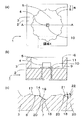
従来、発光素子を収納するためのパッケージとして、例えばセラミックスからなる発光素子収納用パッケージが知られている。図12は従来の発光素子収納用パッケージ102を用いた発光装置101を示す。図12(a)は発光装置101の平面図を示し、図12(b)は図12(a)の点線D−Dにおける断面図を示す。図12(a)および図12(b)において、発光素子収納用パッケージ102は、セラミックスからなる基体103を備え、基体103には、発光素子104が収納される穴部105が設けられている。穴部105の形状は平面視において円形状が一般的である。穴部105の底部109には、発光素子104に電気的に接続される配線導体110が形成されている。そして、発光装置101は、上記発光素子収納用パッケージ102の基体103の穴部105にLED等の発光素子104を収納することによって作製される。発光装置101において、配線導体110を介して発光素子104に電圧をかけることにより、発光素子104はLEDのpn接合領域等において光を放出する。発光素子104から放出された光の一部は、直接穴部105の外部へと放出され、また、発光素子104から放出された光の残りは、内壁111又は底部109において反射された後に、穴部105の外部へと放出される。以上のようにして、発光装置101は光を放出する。
Conventionally, as a package for housing a light emitting element, for example, a light emitting element housing package made of ceramics is known. FIG. 12 shows a
このような発光装置の発光素子収納用パッケージとして、例えば、特許文献1に記載の発光素子収納用パッケージが提案されている。
しかしながら、発光素子の形状や配置、また発光素子と配線導体との接続領域の位置等によって、発光素子から放出される光には、輝度ムラが生じる場合があった。このような場合、従来の発光装置は、穴部の形状が平面視において円形状であったため、発光素子から放出された光が穴部の内壁において均一に反射されてしまい、輝度ムラの生じた光をそのまま放出していた。 However, luminance unevenness may occur in the light emitted from the light emitting element depending on the shape and arrangement of the light emitting element and the position of the connection region between the light emitting element and the wiring conductor. In such a case, in the conventional light emitting device, since the shape of the hole is circular in plan view, the light emitted from the light emitting element is uniformly reflected on the inner wall of the hole, resulting in uneven brightness. The light was emitted as it was.
従って本発明は、上記問題に鑑み、輝度ムラの少ない光を放出する発光装置、その発光装置の製造方法、ならびにその発光装置に用いられる発光素子収納用パッケージ、およびその発光素子収納用パッケージの製造方法を提供することを目的とする。 Therefore, in view of the above problems, the present invention provides a light-emitting device that emits light with less luminance unevenness, a method for manufacturing the light-emitting device, a light-emitting element storage package used in the light-emitting device, and a manufacture of the light-emitting element storage package. It aims to provide a method.
本発明の発光素子収納用パッケージは、発光素子を収納する穴部が設けられた基体を備え、該基体が、平面視した時、前記穴部の開口部に沿って交互に配列する凹部および凸部を有しており、前記穴部の底部が平坦で、前記凹部および前記凸部が前記穴部の開口部から底部に渡って設けられ、前記凹部が曲線からなり、前記穴部が、前記発光素子を搭載する発光素子搭載部を有しており、前記凸部が、平面視した時、前記発光素子搭載部と対向する面を有しており、該面が前記穴部の開口部から底部に渡って設けられ、前記穴部の内面のうち前記凹部の内面のみに金属から成る反射層が設けられていることを特徴とする。
The light emitting element storage package of the present invention includes a base body provided with a hole portion for storing the light emitting element, and when the base body is viewed in a plan view, recesses and protrusions alternately arranged along the opening of the hole portion. The bottom of the hole is flat, the recess and the protrusion are provided from the opening of the hole to the bottom, the recess is a curve, and the hole is the A light-emitting element mounting portion on which the light-emitting element is mounted; and the convex portion has a surface facing the light-emitting element mounting portion when seen in a plan view, and the surface extends from the opening of the hole. A reflective layer made of a metal is provided on only the inner surface of the recess among the inner surface of the hole .
本発明の発光素子収納用パッケージは、好ましくは、全ての前記凹部が、同一形状である。 In the light emitting element storage package of the present invention, preferably, all the concave portions have the same shape.
本発明の発光素子収納用パッケージは、好ましくは、全ての前記凹部が、前記開口部に沿って等間隔に設けられている。 In the light emitting element storage package of the present invention, preferably, all the concave portions are provided at equal intervals along the opening.
本発明の発光素子収納用パッケージは、好ましくは、任意の前記凹部が、他の前記凹部と対向する。 In the light emitting element storage package according to the present invention, preferably, the arbitrary concave portion is opposed to the other concave portion.
本発明の発光素子収納用パッケージは、好ましくは、平面視において、前記凹部の幅が前記凹部の深さより長い。 In the light emitting element storage package of the present invention, preferably, the width of the recess is longer than the depth of the recess in plan view.
本発明の発光素子収納用パッケージは、好ましくは、前記穴部の内壁に、複数の反射層が互いに分離して設けられている。 In the light emitting element storage package of the present invention, preferably, a plurality of reflective layers are provided separately from each other on the inner wall of the hole.
本発明の発光素子収納用パッケージは、好ましくは、前記基体が複数の前記穴部を有する。 In the light emitting element storage package of the present invention, preferably, the base has a plurality of the hole portions.
本発明の発光装置は、本発明の発光素子収納用パッケージと、前記発光素子収納用パッケージの前記穴部に収納される発光素子とを具備することを特徴とする。 The light-emitting device of the present invention includes the light-emitting element storage package of the present invention and a light-emitting element stored in the hole of the light-emitting element storage package.
本発明の発光素子収納用パッケージの製造方法は、前記基体となる第一セラミックグリーンシートおよび第二セラミックグリーンシートを形成するグリーンシート形成工程と、前記第二セラミックグリーンシートに前記穴部の内壁の前記凹部に対応する領域を構成する数の第一貫通孔をそれぞれ形成する第一貫通孔形成工程と、前記第二セラミックグリーンシートに、前記各第一貫通孔を分断し、前記穴部の内壁の前記凸部に対応する領域を構成する第二貫通孔を形成する第二貫通孔形成工程と、前記第一セラミックグリーンシート上に前記第二セラミックグリーンシートを積層する積層工程と、積層した前記第一セラミックグリーンシートおよび前記第二セラミックグリーンシートを焼成する焼成工程と、前記第一貫通孔形成工程の後に、前記複数の第一貫通孔の内壁に反射層を構成する導体ペーストをそれぞれ塗布する塗布工程とを有することを特徴とする。
The method for manufacturing a light emitting element storage package according to the present invention includes a green sheet forming step of forming a first ceramic green sheet and a second ceramic green sheet as the base, and an inner wall of the hole in the second ceramic green sheet. A first through-hole forming step for forming a number of first through-holes constituting a region corresponding to the concave portion, and the first ceramic through holes are divided into the first through-holes, and the inner wall of the hole portion A second through-hole forming step for forming a second through-hole constituting a region corresponding to the convex portion, a laminating step for laminating the second ceramic green sheet on the first ceramic green sheet, and the laminating step a firing step of firing the first ceramic green sheet and the second ceramic green sheet, after the first through-hole forming step, Serial and having a coating step of respectively applying a conductive paste constituting the reflecting layer on the inner wall of a plurality of first through-hole.
本発明の発光素子収納用パッケージの製造方法は、好ましくは、前記第二セラミックグリーンシートが複数枚からなり、前記積層工程において、前記各第二セラミックグリーンシートに形成した第一貫通孔および第二貫通孔が、他の前記第二セラミックグリーンシートに形成した第一貫通孔および第二貫通孔に対応するようにして、前記第一セラミックグリーンシート上に複数の前記第二セラミックグリーンシートを積層する。 In the method for manufacturing a light emitting element storage package according to the present invention, preferably, the second ceramic green sheet is composed of a plurality of sheets, and the first through hole and the second hole formed in each second ceramic green sheet in the stacking step. A plurality of the second ceramic green sheets are laminated on the first ceramic green sheet so that the through holes correspond to the first through holes and the second through holes formed in the other second ceramic green sheets. .
本発明の発光素子収納用パッケージの製造方法は、好ましくは、前記第一貫通孔形成工程において、前記複数の第一貫通孔を前記第二貫通孔の周囲に沿うように形成する。 In the method for manufacturing a light emitting element storage package according to the present invention, preferably, in the first through hole forming step, the plurality of first through holes are formed along the periphery of the second through hole.
本発明の発光装置の製造方法は、本発明の発光素子収納用パッケージの製造方法によって得られる発光素子収納用パッケージを準備する発光素子収納用パッケージ準備工程と、前記発光素子収納用パッケージの前記穴部に、前記発光素子を収納する発光素子収納工程とを有することを特徴とする。 The light emitting device manufacturing method of the present invention includes a light emitting element storing package preparation step of preparing a light emitting element storing package obtained by the method of manufacturing a light emitting element storing package of the present invention, and the hole of the light emitting element storing package. And a light emitting element housing step of housing the light emitting element.
本発明の発光素子収納用パッケージにおける基体は、平面視において、穴部の開口部に沿って交互に配列する凹部および凸部を有する。これにより、本発明の発光素子収納用パッケージは、凹部において光を散乱させるので、本発明の発光素子収納用パッケージに発光素子を収納してなる発光装置は、輝度ムラの少ない光を放出することができる。 The base in the light emitting element storage package of the present invention has recesses and protrusions that are alternately arranged along the opening of the hole in plan view. As a result, the light-emitting element storage package of the present invention scatters light in the recess, so that the light-emitting device in which the light-emitting element is stored in the light-emitting element storage package of the present invention emits light with less luminance unevenness. Can do.
本発明の発光素子収納用パッケージおよびその発光素子収納用パッケージを用いた発光装置の実施の形態について以下に詳細に説明する。 Embodiments of a light-emitting element storage package and a light-emitting device using the light-emitting element storage package of the present invention will be described in detail below.
(第一の実施の形態)
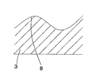
図1は本発明の第一の実施の形態による発光素子収納用パッケージを用いた発光装置を示す。図1(a)は本実施の形態の発光装置1の平面図であり、図1(b)は図1(a)の点線A−Aにおける断面図である。また、図1(c)は図1(a)の領域Xの部分拡大図である。図1において、発光素子収納用パッケージ2は、基体3を備えている。基体3は、発光素子4を収納する穴部5を備えており、平面視したとき、穴部5の開口部6には凹部7および凸部8が設けられている。また、穴部5の底部9には、発光素子4の電極と電気的に接続される配線導体10が形成されている。発光装置1は、上記発光素子収納用パッケージ2の穴部5に発光素子4が収納されてなる。
(First embodiment)
FIG. 1 shows a light-emitting device using a light-emitting element storage package according to a first embodiment of the present invention. FIG. 1A is a plan view of the light-
図1(a)に示すように、基体3には、平面視した時、穴部5の開口部6に沿って交互に配列する凹部7および凸部8が設けられている。凹部7および凸部8が、穴部5の内壁11に沿って、穴部5の開口部6から所定の深さだけ、穴部5の深さ方向に設けられている。凹部7において、穴部5の内壁11は発光素子4から放出された光を反射する際に、光を散乱させる。従って、例えば、発光素子4から放出される光に輝度の強い部位がある場合、その部位に凹部7を配置すると、凹部7において輝度の強い光は散乱するので、輝度の強弱の差を解消し、発光装置1は輝度ムラの少ない光を放出することができる。また、発光素子4から放出される光の輝度の強弱の差が小さい場合は、開口部6に沿って等間隔に凹部7を配置することで、光を穴部5の凹部7により全面的に散乱させ、より輝度ムラの少ない光を放出することができる。なお、本明細書において、開口部とは、基体を平面視した時の、基体と穴部との境界部のことをいう。また、穴部と接する基体の表面は、穴部の内壁と底部とを構成する。また、凹部と凸部との境界部は、凹部の最深部と凸部の先端部とを結んだ直線の中点に最も近い部位とする。
As shown in FIG. 1A, the
ここで、凹部7は、開口部6において、基体3が穴部5の外側に窪んでなる部位のことをいい、平面視したとき、曲線状である。また、穴部5の内壁11において一つの凹部7に対応する領域(以下、「切欠き部」ともいう。)は、曲面状であり、平面方向における任意の断面において曲線状である。このように、凹部7が曲線状であり、また切欠き部が曲面状であることにより、角部を有する場合と比較して、発光素子4から放出された光を均一に散乱させることができる。なお、本明細書において、曲線状とは、角部を持たず、一つの曲線からなり、線上の任意の点における接線の傾きが連続して変化する形状をいう。また、曲面状とは、角部を持たず、一つの曲面からなる形状をいう。
Here, the
また、凸部8は、開口部6において、基体3が穴部5の内側に突出してなる部位のことをいい、略四角形状である。なお、本明細書において、略四角形状とは、図2に示すように、各辺が直線12または曲線13からなり、2つの異なる直線12と直線12、直線12と曲線13、または2つの異なる曲線13と曲線13とが交わってなる角部14を2つ持つ略四角形の外周の一部のことをいい、その設計上、角部14の内角15は45°以上180°未満である。ここで、2つの異なる直線12と直線12とが交わって角部14が形成されている場合、角部14の内角15は、直線12と直線12とがなす角度のことをいう。また、直線12と曲線13とが交わって角部14が形成されている場合、角部14の内角15は、角部14を接点としたときの曲線13の接線16と直線12とがなす角度のことをいう。また、2つの異なる曲線13と曲線13とが交わって角部14が形成されている場合、角部14の内角15は、角部14を接点としたときのそれぞれの曲線13の接線16と接線16とがなす角度のことをいう。なお、好ましくは、上記3つの場合において、角部14の内角15が、90°以上180°未満である。
The
なお、第一の実施の形態においては、図1(c)に示すように、略四角形状の凸部8における、両端に角部14を有する辺17は曲線状である。辺17は、辺17全てを結ぶと略円形となるよう形成されているので、穴部5の内壁11の辺17に対応する領域において、発光素子4から放出された光を一定の反射角で反射することができ、この領域においては光の散乱を低減させる。従って、発光装置1は、内壁11の凹部7に対応する領域においてより光を散乱させ、輝度ムラの少ない光を効率よく放出することができる。
In the first embodiment, as shown in FIG. 1C, the
そして、凸部8の辺17と、この凸部8に隣接する凹部7の境界部20同士を結んだ直線とが重ならないようにすることが好ましい。これらの場合、凸部8の角部14における光の不均一な散乱を低減し、発光装置1は輝度ムラの少ない光を放出できる。なお、図1(c)に示すように、凸部8が略四角形形状である場合、凸部8の2つの角部14のうち、凸部8に隣接する凹部7側の角部14を、凸部8の先端部とする。そして、凸部8に隣接する凹部7側の角部14と凹部7の最深部18とを結んだ直線の中点19に最も近い部位を、凹部7と凸部8との境界部20とする。
It is preferable that the
また、凹部7および凸部8は、穴部5の開口部6から底部9に渡って設けられていることが好ましい。この場合、凹部7は、開口部6から底部9に渡る表面において、光を散乱させることができる。また、図1(b)に示すように、凹部7における内壁11は、底部9に対して垂直であり、穴部5の開口部6から底部9に渡って直線状である。内壁11が直線状であることにより、発光素子4から穴部5の内壁11方向に放出された光のうち、発光素子4の発光面よりも基体1の上面側に放出された光を、底部9側に向かって反射することを抑制し、基体3の上面側に向かって反射することができるので、発光装置1から放出される光の輝度の低減を抑制することができる。なお、内壁11が直線状とは、内壁11の表面が微小な凹凸を有していてもよい。例えば、内壁11の表面が微小な凹凸を有する場合、発光素子4から放出された光を底部9に向かって反射することを抑制できればよく、凹凸の段差が10μm以下程度にしておくことが好ましい。
Moreover, it is preferable that the
また、穴部5の底部9は平坦であり、例えば、複数の発光素子4が収納される場合は、発光素子4間にしきりがない。底部9が平坦であると、それぞれの発光素子4から放出された光は穴部5全体に分散し、穴部5の内壁11において反射するので、良好に光を散乱させ、発光装置1は、輝度ムラの少ない光を放出することができる。なお、本明細書において、底部が平坦であるとは、それぞれの発光素子から放出された光を遮るしきりが底部にないことを示し、底部が曲面であったり、屈曲していたり、光を遮らない程度の微小な凹凸を有してもよい。
Further, the
なお、本実施の形態による発光装置1においては、発光素子4から放出される光の輝度にばらつきがある場合、凹部7は、光の輝度が強い領域と一致するように設けられている。例えば、発光素子4と配線導体10との接続領域に大きな電流が流れると、その領域の光の輝度は他の領域の光の輝度と比べて高くなる場合がある。また、発光素子4の形状により、発光素子4から放出される光に輝度の差が生じる場合もある。これらの場合、凹部7を光の輝度が強い領域と一致するように配置すると、凹部7において輝度の強い部位の光が散乱する。従って、光の輝度の強弱の差が減り、発光装置1は輝度ムラの少ない光を放出させることができる。
In the
穴部5の内壁11において、光の輝度ムラが生じる場合として、例えば、光の輝度ムラが対称的に生じる場合がある。この場合、凹部7が他の凹部7と対向していると、輝度が強い領域に凹部7を配置させることができるので、発光装置1は輝度ムラの少ない光を放出することができる。
As a case where uneven brightness of light occurs in the
また、穴部5の内壁11において、光の輝度の強弱の差が同程度である場合もある。この場合、全ての凹部7は、平面視において、同一形状であると、各領域における光の輝度の強弱の差を同程度に緩和させることができるので、発光装置1はムラの少ない光を放出することができる。
Further, in the
また、穴部5の内壁11において、光の輝度ムラが等間隔に生じる場合もある。この場合、全ての凹部7が、平面視において、穴部5の開口部6に沿って等間隔に設けられていると、輝度が強い領域に凹部7を配置させることができるので、発光装置1は輝度ムラの少ない光を放出することができる。
In addition, in the
なお、穴部5の内壁11において、光の輝度の強弱の差が少ない場合には、全ての凹部7は、平面視において、同一形状であるとよい。各領域における光の輝度の強弱の差を同程度に緩和させることができるので、発光装置1は輝度ムラの少ない光を放出することができる。また、全ての凹部7が、平面視において、穴部5の開口部6に沿って等間隔に設けられていてもよい。穴部5の内壁11の特定の偏った領域の凹部7において、光が散乱することはないので、発光装置1は輝度ムラの少ない光を放出することができる。
In addition, in the
また、図1(c)に示すように、平面視における凹部7の形状は、凹部7の幅21が凹部7の深さ22より長い。凹部7の幅21を凹部7の深さ22より長くすることにより、輝度ムラの少ない光を放出しつつ、発光素子収納用パッケージ2を小型化することができる。なお、本明細書において、凹部の幅とは、凹部の両端の境界部間の距離のことをいい、凹部の深さとは凹部の幅となる直線と凹部の最深部との最短距離のことをいう。
Further, as shown in FIG. 1 (c), the shape of the
基体3は、例えばセラミックスや樹脂などの絶縁材料からなる。なお、発光素子4から放出された光を効率良く反射することができるので、絶縁材料は白色であるとよい。セラミックスからなる場合、基体3は、例えば、酸化アルミニウム質焼結体、窒化アルミニウム質焼結体、ムライト質焼結体、またはガラスセラミックス等からなるセラミック層が複数層積層してなる。このように積層することにより、配線導体10を基体3の内部に3次元的に配線できるので、配線の高密度化および発光素子収納用パッケージ2の小型化が可能となる。
The
基体3の穴部5の底部9には、発光素子4の電極が電気的に接続される配線導体10が形成されている。発光素子4の電極は、配線導体10に、例えば、ワイヤボンディング方式またはフリップチップ方式で電気的に接続されている。配線導体10は、タングステン、モリブデン、銅、または銀等の金属粉末を焼成して得られたメタライズにより形成される。なお、配線導体10の露出する表面には、電解めっき法または無電解めっき法により、ニッケル、金、銀、白金、またはパラジウム等のめっき金属層を被着することが好ましい。
A
穴部5に収納される発光素子4は、1つであっても複数であってもよい。特に、異なる波長の光を放出する複数の発光素子4を用いる場合、凹部7において光が散乱することにより、発光装置1から放出される光の色調ムラを低減させることができる。例えば、発光素子4として赤色LEDと緑色LEDと青色LEDを用いた場合、本実施の形態の発光装置1は、色調ムラの少ない白色光を放出することができる。なお、配線導体10は、複数の発光素子4に合わせてそれぞれ形成される。
The
なお、第一の実施の形態において、平面視における穴部5の形状は、開口部6に沿って交互に配列する凹部7および凸部8を有する円形状であるとしたが、開口部6に沿って交互に配列する凹部7および凸部8を有していればよく、楕円形状、長円形状、略多角形状等でもよい。
In the first embodiment, the shape of the
また、凹部7は曲線状であるとしたが、曲線状とは限らず、略四角形状または略四角形状以外の略多角形状等でもよい。例えば、発光素子収納用パッケージに小型化が求められる場合、凹部を、両端に角部を有する辺が直線である略四角形状とすると、凹部の深さを小さくすることができるので、発光素子収納用パッケージを小型化できる。なお、本明細書において、略四角形状以外の略多角形状とは、各辺が直線または曲線からなり、2つの異なる直線と直線、直線と曲線、または2つの異なる曲線と曲線とが交わってなる角部を3つ以上持つ略多角形の外周の一部のことをいい、その設計上、角部の内角は45°以上180°未満である。なお、略四角形状以外の略多角形状の角部の内角は、略四角形状の角部の内角と同様の部位の角度のことをいう。
In addition, the
図3は本発明の第一の実施の形態による発光素子収納用パッケージ2を用いた発光装置1の変形例を示す部分拡大図である。図1において、凸部8は、曲線状である辺17を有する略四角形状であるとしたが、図3に示すように、凸部8は、曲線状でもよい。また、凸部8は、略四角形以外の略多角形状等でもよい。このように凸部8が略四角形以外の略多角形状または曲線状であることにより、凸部8において光は均一に散乱し、発光装置1から放出される光の輝度ムラを低減できる。
FIG. 3 is a partially enlarged view showing a modification of the
なお、凹部7および凸部8は、穴部5の開口部6から底部9に渡って設けられているとは限らず、断面視において、穴部5の内壁11の一部に設けられていてもよい。
Note that the
また、図1(b)において、断面視における穴部5の内壁11は、底部9に対して垂直であるが、傾斜していてもよい。図4は本発明の第一の実施の形態による発光素子収納用パッケージ2を用いた発光装置1の変形例を示す断面図である。この発光素子収納用パッケージ2の基体3の穴部5は、底部9側から基体3の上面側に向かって広がっている。これにより、発光素子4から放出される光を外部に均一かつ効率良く放出することができ、発光装置1の発光効率を高めることができる。なお、本変形例において、底部9側から基体3の上面側に向かって穴部5全体が広がっていてもよいし、穴部5のうち凹部に対応する領域のみが広がっているか、または、凸部に対応する領域のみが広がっていてもよい。
Further, in FIG. 1B, the
また、発光素子収納用パッケージ2の基体3の穴部5は、発光装置1の用途により、底部9側から基体3の上面側に向かって狭くなっていてもよく、放出される光の正面方向への指向性を高め、正面からの視認性を高めることができる。また、異なる波長の光を放出するために複数の発光素子4を用いる場合、穴部5内における光の反射回数が増えるため、発光装置1から放出される光の色調ムラを低減できる。
Further, the
また、図1(b)において、配線導体10は、穴部5の底部9に形成されているが、配線導体10は、基体3の上面に形成されていてもよい。また、一方の配線導体10を穴部5の底部9に形成し、他方の配線導体10を基体3の上面に形成しても構わない。これらの場合には、例えば、穴部に収容された発光素子の電極と基体の上面に形成された配線導体とが、ワイヤボンディング方式等により電気的に接続される。このように、配線導体が基体の上面に形成される場合には、配線導体を底部に形成しないため、平面視において穴部の径を小さくすることができる。これにより、穴部の内壁と発光素子の距離を短くすることができるため、穴部において発光素子から放出される光の輝度の低減を抑制でき、発光装置から放出される光の輝度を向上させることができる。
In FIG. 1B, the
さらに、枠体が基体の上面に配置されていると、枠体の開口に封止部材を充填することができるため、基体の上面に形成された配線導体が枠体の開口に充填された封止部材により保護され、発光装置の信頼性をより向上させることができる。ここで、枠体が基体の上面に配置されている発光素子収納用パッケージを用いた発光装置を図5に示す。図5(a)は発光装置1の平面図であり、図5(b)は図5(a)の点線B−Bにおける断面図である。図5に示す発光装置1は、開口23を有する枠体24が基体3の上面に配置されている。そして、配線導体10は基体3の上面に形成されており、穴部5に収容された発光素子4の電極と配線導体10とがワイヤ線25により電気的に接続されている。なお、枠体24は、枠体24の下方側から上方側に向かって広がるように、枠体24の内壁を傾斜させておいても構わない。これにより、発光素子4から放出される光を外部に効率良く放出することができ、発光装置1の発光効率を高めることができる。
Further, when the frame body is arranged on the upper surface of the base body, the sealing member can be filled in the opening of the frame body. Therefore, the wiring conductor formed on the upper surface of the base body is sealed in the opening of the frame body. It is protected by the stop member, and the reliability of the light emitting device can be further improved. Here, FIG. 5 shows a light-emitting device using a light-emitting element storage package in which a frame is arranged on the upper surface of a base. 5A is a plan view of the
なお、枠体24は、例えば、セラミックス、樹脂、もしくは金属材料からなる。枠体24が絶縁材料からなる場合、基体3の場合と同様な理由により、白色であるとよい。また、枠体24が金属材料からなる場合、枠体24は、ニッケル、金、銀、白金、もしくはパラジウム等の金属材料、または、表面にニッケル、金、銀、白金、もしくはパラジウム等のめっき層が被着されたCu,Cu−W,Fe−Ni,もしくはFe−Ni−Co等の金属材料等を好適に使用することができる。これにより、発光素子4から放出される光を枠体24においても良好に反射させることができる。なお、枠体24がセラミックスからなる場合、後述する基体3の製造方法と同様の方法を用いることにより製作することができる。なお、基体3と枠体24とは接合材により接合される。例えば、基体3がセラミックス材料からなり、枠体24が金属材料からなる場合には、基体3の上面に接合用金属層を形成しておき、この接合用金属層と枠体24とをAg−Cuろう材等のろう材を用いて接合させればよい。また、基体3と枠体24とがともにセラミックス材料からなる場合、焼結することにより基体3と枠体24とを一体化させても構わない。また、基体3と同様に、平面視した時、枠体24の内壁に交互に配列する凹部および凸部を形成しておいても構わない。
The
また、これまで説明した図1(b)、図4、および図5(b)において、配線導体10は、基体3の下面に引き出されて外部電気回路基板の配線に接続されているが、基体3の側面あるいは上面に引き出されて外部電気回路基板の配線に接続されていてもよい。配線導体10の配置は、発光素子4の電極との接続や外部電気回路基板の配線との接続等を考慮して決定される。
Further, in FIGS. 1B, 4 and 5B described so far, the
また、図1において、発光素子収納用パッケージ2には、穴部5が一つ設けられているが、複数設けられていてもよい。図6は本発明の第一の実施の形態による発光素子収納用パッケージを用いた発光装置1の変形例を示す平面図である。輝度の高い光が求められる場合、図1に示す発光装置1が複数用いられてもよいが、図6に示す発光装置1は、一つの基体3に穴部5が複数設けられているので、発光装置1一つで、図1の発光装置1を複数用いた場合と同程度の輝度の光を放出できる。
In FIG. 1, the light emitting
また、発光素子4は、好ましくは、封止部材により封止されている。封止部材は、例えば、発光素子4を包囲したり、発光素子4の上方を覆ったり、又は穴部5に充填されたりすることにより、発光素子4を封止する。また、発光素子4の電極をワイヤボンディング方式により配線導体10に接続する場合、ワイヤ線も封止部材により同様に封止される。なお、封止部材が穴部5に充填されている場合、発光素子収納用パッケージ2の基体3は、平面視した時、穴部5の開口部6に沿って交互に配列する凹部7および凸部8が設けられているので、封止部材と穴部5の内壁11との接触面積が増え、接合強度が大きくなるので、発光素子4の発熱による封止部材の剥離を抑制できる。なお、封止部材は、例えばシリコーン樹脂若しくはエポキシ樹脂等の光透過性の透明樹脂、又はガラス等の光透過性の無機材料等からなる。
The
次に、本発明の第一の実施の形態による発光素子収納用パッケージの製造方法について、図7に基づいて説明する。図7は図1に示した発光素子収納用パッケージ2を製造する製造工程を示す。
Next, the manufacturing method of the light emitting element accommodation package by 1st embodiment of this invention is demonstrated based on FIG. FIG. 7 shows a manufacturing process for manufacturing the light emitting
まず、基体となる第一セラミックグリーンシート、および第二セラミックグリーンシートを形成する。なお、第一セラミックグリーンシートおよび第二セラミックグリーンシートは一枚でも複数枚でもよい。このようなセラミックグリーンシートは、例えばセラミックスが酸化アルミニウム質焼結体からなる場合、酸化アルミニウム、酸化珪素、酸化カルシウム、または酸化マグネシウム等のセラミック原料粉末に適当な有機バインダー、溶剤、可塑剤、および分散剤等を添加混合して泥漿とし、これを公知のドクターブレード法等のシート成形技術により所定厚みのシート状とすることによって作製される。 First, a first ceramic green sheet and a second ceramic green sheet to be a base are formed. The first ceramic green sheet and the second ceramic green sheet may be one sheet or a plurality of sheets. Such a ceramic green sheet is, for example, when the ceramic is made of an aluminum oxide sintered body, an organic binder, a solvent, a plasticizer, and a suitable ceramic raw material powder such as aluminum oxide, silicon oxide, calcium oxide, or magnesium oxide, and It is produced by adding a dispersing agent or the like to make a slurry, which is formed into a sheet having a predetermined thickness by a sheet forming technique such as a known doctor blade method.
次に、図7(a)に示すように、第二セラミックグリーンシート26に、打ち抜き金型を用いて、穴部の内壁の凹部に対応する領域を構成する複数の第一貫通孔27を打ち抜く。このように打ち抜き金型で打ち抜くことにより、凹部を容易に形成することができる。
Next, as shown in FIG. 7A, a plurality of first through
なお、後に形成される第二貫通孔28の周囲に沿うようにして、例えば、円形状に並ぶように各第一貫通孔27を形成すると、基体において所望の凹部を正確に形成することができる。
In addition, if each 1st through-
次に、図7(b)に示すように、第二セラミックグリーンシート26に、穴部の内壁の凹部に対応する領域を構成する第二貫通孔28を、全ての第一貫通孔27を分断するように、打ち抜き金型を用いて打ち抜く。
Next, as shown in FIG. 7 (b), the second ceramic
次に、図7(c)に示すように、第一セラミックグリーンシート29上に、第二セラミックグリーンシート26を積層する。ここでは、第二セラミックグリーンシート26に形成された第一貫通孔27および第二貫通孔28が、他の第二セラミックグリーンシート26の第一貫通孔27および第二貫通孔28に連通するように、第二セラミックグリーンシート26を積層するとよい。これにより、凹部を穴部の開口部から底部に渡って形成することができる。
Next, as shown in FIG. 7C, the second ceramic
なお、凹部が穴部の開口部から底部に渡って設けられているのではなく、断面視において、穴部の内壁の一部に設けられている場合は、第一貫通孔27および第二貫通孔28が形成された第二セラミックグリーンシート26と、第二貫通孔28のみが形成された第二セラミックグリーンシート26とを、第一貫通孔27が凹部の位置に配置されるように、適宜積層すればよい。
In addition, when the concave portion is not provided from the opening portion of the hole portion to the bottom portion but is provided in a part of the inner wall of the hole portion in a sectional view, the first through
最後に、積層されたセラミックグリーンシートの積層体を焼成することによって、セラミックスの焼結体からなる基体を得る。以上より図1に示した発光素子収納用パッケージ2が完成する。
Finally, the laminated body of the laminated ceramic green sheets is fired to obtain a substrate made of a ceramic sintered body. Thus, the light emitting
なお、図示していないが、配線導体を形成するため、第一貫通孔または第二貫通孔とは別に、配線導体用貫通孔を第一セラミックグリーンシート29に打ち抜き金型を用いて打ち抜く。そして、穴部の底部および基体の下面に配線導体を形成する場合には、スクリーン印刷法等の厚膜形成法により、第一セラミックグリーンシート29の主面に配線導体用金属ペーストを塗布する。また、基体の内部に配線導体を形成する場合には、配線導体用貫通孔に配線導体用金属ペーストを充填する。そして、焼成工程において、配線導体用金属ペーストを、第一セラミックグリーンシート29および第二セラミックグリーンシート26と同時焼成することにより、配線導体10を形成する。なお、配線導体用金属ペーストは、発光素子収納用パッケージに形成される配線導体の位置に合わせて、塗布または充填されていればよい。例えば、基体の上面に配線導体を形成する場合、または配線導体の一部が穴部の内壁に露出するように配線導体を形成する場合、第二セラミックグリーンシート26の主面に配線導体用金属ペーストを塗布すればよい。
Although not shown, in order to form a wiring conductor, a wiring conductor through hole is punched into the first ceramic
そして、上記の発光素子収納用パッケージの穴部に発光素子を収納し、発光素子の電極と配線導体とを電気的に接続する。そして、好ましくは、封止部材によって発光素子を封止する。以上より図1に示した発光装置1が完成する。
And a light emitting element is accommodated in the hole of said light emitting element accommodation package, and the electrode and wiring conductor of a light emitting element are electrically connected. Preferably, the light emitting element is sealed with a sealing member. Thus, the
上記の発光素子収納用パッケージの製造方法によれば、輝度ムラの少ない光を放出する発光素子収納用パッケージを容易に作製できる。また、本実施の形態の製造方法においては、穴部の形成において、第一貫通孔27と第二貫通孔28とを別々の打ち抜き金型により形成する。このように単純な形状の打ち抜き金型を複数組み合わせることで、複雑な形状の穴部を形成することができるため、容易に打ち抜き金型を作製できるとともに、複雑な形状の穴部を簡便に形成することができる。
According to the above method for manufacturing a light emitting element storage package, it is possible to easily manufacture a light emitting element storage package that emits light with less luminance unevenness. In the manufacturing method of the present embodiment, the first through
なお、各貫通孔は打ち抜き金型により形成するとしたが、例えばレーザー加工等の貫通孔形成手段を用いて形成してもよい。 Although each through hole is formed by a punching die, it may be formed by using a through hole forming means such as laser processing.
また、配線導体用貫通孔を第一セラミックグリーンシート29に打ち抜くとしたが、第二セラミックグリーンシート26に打ち抜いてもよい。これにより、例えば、基体の上面に配線導体を引き出すことができる。
Further, although the wiring conductor through hole is punched into the first ceramic
(第二の実施の形態)
図8は本発明の第二の実施の形態による発光素子収納用パッケージを用いた発光装置を示す。図8(a)は本実施の形態の発光装置の平面図であり、図8(b)は図8(a)の点線C−Cにおける断面図である。この発光素子収納用パッケージの基体3の表面には、凹部7に対応する領域と凸部8に対応する一部の領域において反射層30が設けられている。
(Second embodiment)
FIG. 8 shows a light emitting device using the light emitting element storage package according to the second embodiment of the present invention. FIG. 8A is a plan view of the light-emitting device of this embodiment, and FIG. 8B is a cross-sectional view taken along the dotted line CC in FIG. On the surface of the
その他の構成については、第一の実施の形態と同様の構成であるので、同一の符号を付し、説明を省略する。 Since other configurations are the same as those in the first embodiment, the same reference numerals are given and description thereof is omitted.
反射層30は、メタライズ金属層31にめっき金属層32が被着されてなる。メタライズ金属層31は、例えばタングステン、モリブデン、銅、または銀等の金属粉末を焼成して得られたメタライズからなる。また、めっき金属層32は、ニッケル、金、銀、白金、またはパラジウム等からなる。めっき金属層32は、発光素子収納用パッケージの内壁11における光の反射効率を上昇させることができるとともに、メタライズ金属層31が酸化して反射効率が低下することを抑制できる。従って、発光装置から放出される光の輝度を向上させることができる。
The
反射層30を形成する場合、穴部5の内壁11に複数の反射層30を互いに分離して形成するとよい。このような構成にすると、複数の配線導体10がそれぞれ異なる反射層30に接触したとしても、各反射層30が電気的に接続されないので、配線導体10間の短絡を抑制することができる。従って、信頼性が向上するとともに、配線導体10を反射層30に近づけて設置できるので、発光素子収納用パッケージを小型化できる。さらに、配線導体10は光を効率よく反射するので、配線導体10を反射層30に近づけて設置すると、底部9における配線導体10の占める割合が増え、光の反射効率が向上する。
When forming the
また、図8(a)に示すように、穴部5の内壁11の凹部7に対応する領域において、反射層30を形成すると、反射層30が穴部5の内側にせり出さないので、発光素子収納用パッケージを小型化できる。さらに、反射層30と配線導体10とが接触しにくくなるため、発光装置の信頼性を向上させることができる。なお、反射層30は凹部7と凸部8との境界部をこえて設けられてもよく、反射層30が凸部8の角部または先端部より穴部5の内側にせり出さないように設けられればよい。この場合、発光素子収納用パッケージを小型化できる。
Further, as shown in FIG. 8A, when the
また、第二の実施の形態において、反射層30はメタライズ金属層31にめっき金属層32を被着してなるとしたが、反射層30はメタライズ金属層31のみから形成されていてもよい。
In the second embodiment, the
次に、本発明の第二の実施の形態による発光素子収納用パッケージの製造方法について、図9に基づいて説明する。図9は図8に示した発光素子収納用パッケージを製造する製造工程を示す。 Next, the manufacturing method of the light emitting element storage package by 2nd embodiment of this invention is demonstrated based on FIG. FIG. 9 shows a manufacturing process for manufacturing the light emitting element storage package shown in FIG.
まず、図9(a)に示すように、図7に示した発光素子収納用パッケージの製造工程と同様に、グリーンシート形成工程、および第二セラミックグリーンシート26への第一貫通孔形成工程を行なう。
First, as shown in FIG. 9A, the green sheet forming step and the first through hole forming step in the second ceramic
次に、図9(b)に示すように、各第一貫通孔27の内壁に、メタライズ金属層31を形成する導体ペースト33を、スクリーン印刷法等の厚膜法により塗布する。なお、印刷塗布の際には、印刷面の反対側から導体ペースト33を吸引しながら印刷する。この製造方法によると、厚膜法により導体ペースト33を各第一貫通孔27の内壁に塗布する際に、貫通方向に均一に塗布できるので、凹部において、メタライズ金属層31が基体の表面に、穴部の底部から開口部に渡って均一に形成された発光素子収納用パッケージを作製することができる。
Next, as shown in FIG. 9B, a
そして、図示していないが、図7に示した発光素子収納用パッケージの製造方法と同様に、図9(c)に示す第二貫通孔形成工程の後、積層工程、焼成工程を順に行ない、メタライズ金属層31が形成されたセラミックスの焼結体からなる基体を得る。
And although not shown, like the method for manufacturing the light emitting element storage package shown in FIG. 7, after the second through-hole forming step shown in FIG. A substrate made of a ceramic sintered body on which the metallized
なお、図示していないが、配線導体を形成するため、本発明の第一の実施の形態による発光素子収納用パッケージの製造工程と同様に、配線導体用貫通孔を形成し、第一セラミックグリーンシート29の主面に配線導体用金属ペーストを塗布するとともに配線導体用貫通孔に配線導体用金属ペーストを充填する。そして、焼成工程において、配線導体用金属ペーストを、第一セラミックグリーンシート29および第二セラミックグリーンシート26と同時焼成する。
Although not shown, in order to form a wiring conductor, a through hole for the wiring conductor is formed in the same manner as in the manufacturing process of the light emitting element storage package according to the first embodiment of the present invention. A wiring conductor metal paste is applied to the main surface of the
また、めっき金属層32が形成される場合、図9(d)に示すように、基体3のメタライズ金属層31の露出する表面に電解めっき法や無電解めっき法により、ニッケル、金、銀、白金、またはパラジウム等のめっき金属層32を被着させる。
When the plated
以上の製造方法により、発光素子収納用パッケージの穴部5の内壁の凹部7に対応する領域において、反射層30を容易に形成することができる。
By the above manufacturing method, the
なお、本実施の形態の発光素子収納用パッケージの製造方法においては、凹部に対応する領域と凸部に対応する一部の領域において反射層30を形成したが、穴部5の内壁11において、全面的に反射層30を形成しても構わない。すなわち、凹部7に対応する領域とともに、凸部8に対応する領域において、反射層30を形成しても構わない。この場合、第一貫通孔27の内壁に反射層30を形成し、第二貫通孔28を形成した後、第一貫通孔27の内壁に反射層30を形成する場合と同様な方法を用いて、第二貫通孔28の内壁に反射層30を形成すればよい。
In the method for manufacturing the light emitting element storage package of the present embodiment, the
また、本発明の第二の実施の形態による発光素子収納用パッケージの製造方法において、反射層30は厚膜法およびめっき法により形成するとしたが、薄膜法により形成してもよい。薄膜法により形成する場合、例えば、図7に示した発光素子収納用パッケージの製造方法と同様に、グリーンシート形成工程、第一貫通孔形成工程、第二貫通孔形成工程、積層工程、および焼成工程を行なった後、蒸着またはスパッタリング等の薄膜法によって薄膜からなる金属層を形成する。めっき金属層を形成する場合は、薄膜からなる金属層を形成した後、図9(d)に示した発光素子収納用パッケージの製造方法と同様に形成する。
In the method for manufacturing the light emitting element storage package according to the second embodiment of the present invention, the
図10は本発明の第二の実施の形態による発光素子収納用パッケージを用いた発光装置の変形例を示す平面図である。図8に示す発光装置においては、反射層30が、凹部7に対応する領域と凸部8に対応する一部の領域とに形成されているが、図10に示す発光装置においては、反射層30が、穴部5の内壁の凹部7に対応する領域のみに設けられている。
FIG. 10 is a plan view showing a modification of the light emitting device using the light emitting element storage package according to the second embodiment of the present invention. In the light emitting device shown in FIG. 8, the
次に、本発明の第二の実施の形態の変形例による発光素子収納用パッケージの製造方法について、図11に基づいて説明する。図11は図10に示した発光素子収納用パッケージを製造する製造工程を示す。 Next, the manufacturing method of the light emitting element storage package by the modification of 2nd Embodiment of this invention is demonstrated based on FIG. FIG. 11 shows a manufacturing process for manufacturing the light emitting element storage package shown in FIG.
まず、図11(a)に示すように、第一の実施の形態で説明した発光素子収納用パッケージの製造工程と同様にグリーンシート形成工程を行なった後、第二セラミックグリーンシート26に打ち抜き金型を用いて、反射層を構成する複数の第三貫通孔34を打ち抜く。
First, as shown in FIG. 11A, after the green sheet forming process is performed in the same manner as the manufacturing process of the light emitting element storage package described in the first embodiment, the second ceramic
次に、図11(b)に示すように、各第三貫通孔34に、メタライズ金属層を形成する導体ペースト33を、スクリーン印刷法等の厚膜法により充填する。導体ペースト33の充填によりメタライズ金属層を形成するため、第三貫通孔34は小さく形成することができる。
Next, as shown in FIG. 11B, each third through
次に、図11(c)に示すように、第二セラミックグリーンシート26に、打ち抜き金型を用いて、第三貫通孔34を分断するように、各第一貫通孔27を打ち抜く。
Next, as shown in FIG. 11C, each first through
次に、図11(d)に示すように、図7に示した発光素子収納用パッケージの製造工程と同様に、全ての第一貫通孔27を分断するように第二貫通孔形成工程行なう。
Next, as shown in FIG. 11 (d), the second through hole forming step is performed so as to divide all the first through
そして、図示していないが、図7に示した発光素子収納用パッケージの製造方法と同様に、図11(d)に示す第二貫通孔形成工程の後、積層工程、焼成工程を順に行ない、メタライズ金属層が形成されたセラミックスの焼結体からなる基体を得る。
And although not shown in figure, like the manufacturing method of the light emitting element accommodation package shown in
なお、図示していないが、配線導体を形成するため、本発明の第一の実施の形態による発光素子収納用パッケージの製造工程と同様に、第一貫通孔形成工程または第二貫通孔形成工程において、配線導体用貫通孔を形成し、第一セラミックグリーンシート29の主面に配線導体用金属ペーストを塗布するとともに配線導体用貫通孔に配線導体用金属ペーストを充填する。そして、焼成工程において、配線導体用金属ペーストを、第一セラミックグリーンシート29および第二セラミックグリーンシート26と同時焼成する。
Although not shown, in order to form the wiring conductor, the first through-hole forming step or the second through-hole forming step is performed in the same manner as the manufacturing process of the light emitting element storage package according to the first embodiment of the present invention. The wiring conductor through-hole is formed, the wiring conductor metal paste is applied to the main surface of the first ceramic
また、めっき金属層が形成される場合、図9(d)に示した発光素子収納用パッケージの製造方法と同様に、基体のメタライズ金属層の露出する表面にめっき金属層を被着させる。 When the plated metal layer is formed, the plated metal layer is deposited on the exposed surface of the metallized metal layer of the substrate in the same manner as in the method for manufacturing the light emitting element storage package shown in FIG.
以上の製造方法により、発光素子収納用パッケージの内壁の凹部に対応する領域において、反射層を容易に形成することができる。また、第三貫通孔34に導体ペースト33を充填するため、小型の凹部に反射層を形成しやすい。したがって、反射層が設けられた小型の凹部を多数形成して、輝度ムラを低減した光を放出可能な発光装置を作製する場合に、この製造方法は特に有効である。
With the above manufacturing method, the reflective layer can be easily formed in the region corresponding to the concave portion of the inner wall of the light emitting element storage package. In addition, since the third through
なお、本発明は上記の実施の形態に限定されるものではなく、本発明の要旨を逸脱しない範囲内で種々の変更を行ってもよい。例えば、基体3の一部に金属部材を用いたものであっても構わない。例えば、基体3の底部9よりも上面側の部材、すなわち穴部5の凸部7と凹部8の領域を形成する部材を金属材料から形成しても構わない。この場合、ニッケル、金、銀、白金、もしくはパラジウム等の金属材料、または、表面にニッケル、金、銀、白金、もしくはパラジウム等のめっき層が被着されたCu,Cu−W,Fe−Ni,もしくはFe−Ni−Co等の金属材料等を好適に使用することができる。なお、基体3の底部9側の部材と上面側の部材とを接合材を用いて接合させればよい。例えば、基体3の底部9側の部材がセラミックスからなる場合、基体3の底部9側の部材上に接合用金属層を形成しておき、この接合用金属層と上面側の部材とをAg−Cuろう材等のろう材を用いて接合させればよい。また、基体3の底部9側の一部に金属部材を使用しても構わない。また、本発明の図面において、便宜上、図面の縮尺は変更して記載している。
In addition, this invention is not limited to said embodiment, You may make a various change within the range which does not deviate from the summary of this invention. For example, a metal member may be used for a part of the
1 発光装置
2 発光素子収納用パッケージ
3 基体
4 発光素子
5 穴部
6 開口部
7 凹部
8 凸部
9 底部
10 配線導体
11 内壁
26 第二セラミックグリーンシート
27 第一貫通孔
28 第二貫通孔
29 第一セラミックグリーンシート
30 反射層
31 メタライズ金属層
32 めっき金属層
33 導体ペースト
DESCRIPTION OF
Claims (12)
該基体が、平面視した時、前記穴部の開口部に沿って交互に配列する凹部および凸部を有しており、
前記穴部の底部が平坦で、前記凹部および前記凸部が前記穴部の開口部から底部に渡って設けられ、前記凹部が曲線からなり、
前記穴部が、前記発光素子を搭載する発光素子搭載部を有しており、
前記凸部が、平面視した時、前記発光素子搭載部と対向する面を有しており、該面が前記穴部の開口部から底部に渡って設けられ、
前記穴部の内面のうち前記凹部の内面のみに金属から成る反射層が設けられていることを特徴とする発光素子収納用パッケージ。 A substrate provided with a hole for accommodating the light emitting element;
The base body has concave and convex portions that are alternately arranged along the opening of the hole when viewed in plan,
The bottom of the hole is flat, the recess and the protrusion are provided from the opening of the hole to the bottom, the recess is a curve,
The hole has a light emitting element mounting portion for mounting the light emitting element;
The convex portion has a surface facing the light emitting element mounting portion when seen in a plan view, and the surface is provided from the opening of the hole to the bottom ,
A light emitting element storage package, wherein a reflective layer made of a metal is provided only on the inner surface of the concave portion of the inner surface of the hole .
前記発光素子収納用パッケージの前記穴部に収納される発光素子とを具備する発光装置。 The light emitting element storage package according to any one of claims 1 to 7 ,
A light emitting device comprising: a light emitting element housed in the hole of the light emitting element housing package.
の開口部に沿って交互に配列する凹部および凸部を有しており、前記穴部の底部が平坦で、前記凹部および前記凸部が前記穴部の開口部から底部に渡って設けられ、前記凹部が曲線からなり、前記穴部が、前記発光素子を搭載する発光素子搭載部を有しており、前記凸部が、平面視した時、前記発光素子搭載部と対向する面を有しており、該面が前記穴部の開口部から底部に渡って設けられ、前記穴部の内面のうち前記凹部の内面のみに金属から成る反射層が設けられている発光素子収納用パッケージの製造方法であって、
前記基体となる第一セラミックグリーンシートおよび第二セラミックグリーンシートを形成するグリーンシート形成工程と、
前記第二セラミックグリーンシートに、前記穴部の内壁の前記凹部に対応する領域を構成する複数の第一貫通孔をそれぞれ形成する第一貫通孔形成工程と、
前記第二セラミックグリーンシートに、前記各第一貫通孔を分断し、前記穴部の内壁の前記凸部に対応する領域を構成する第二貫通孔を形成する第二貫通孔形成工程と、
前記第一セラミックグリーンシート上に前記第二セラミックグリーンシートを積層する積層工程と、
積層した前記第一セラミックグリーンシートおよび前記第二セラミックグリーンシートを焼成する焼成工程と、
前記第一貫通孔形成工程の後に、前記複数の第一貫通孔の内壁に反射層を構成する導体ペーストをそれぞれ塗布する塗布工程とを有する発光素子収納用パッケージの製造方法。 A base provided with a hole for accommodating the light emitting element, and the base has a concave portion and a convex portion alternately arranged along the opening of the hole when viewed in plan, and the hole A bottom portion of the light emitting element mounting portion on which the concave portion and the convex portion are provided from the opening portion of the hole portion to the bottom portion, the concave portion is formed of a curve, and the hole portion mounts the light emitting element. The convex portion has a surface facing the light emitting element mounting portion when seen in a plan view, and the surface is provided from the opening to the bottom of the hole, and the hole A method for manufacturing a light emitting element storage package in which a reflective layer made of metal is provided only on the inner surface of the recess among the inner surfaces of
A green sheet forming step of forming a first ceramic green sheet and a second ceramic green sheet as the base;
In the second ceramic green sheet, a first through-hole forming step for forming a plurality of first through-holes each constituting a region corresponding to the concave portion of the inner wall of the hole portion;
A second through-hole forming step of dividing the first through-holes into the second ceramic green sheet and forming second through-holes constituting regions corresponding to the convex portions of the inner walls of the hole portions;
A laminating step of laminating the second ceramic green sheet on the first ceramic green sheet;
A firing step of firing the first ceramic green sheet and the second ceramic green sheet laminated ;
The manufacturing method of the package for light emitting element accommodation which has an application | coating process which apply | coats the conductor paste which comprises a reflection layer on the inner wall of these 1st through-holes after said 1st through-hole formation process, respectively .
前記発光素子収納用パッケージの前記穴部に、前記発光素子を収納する発光素子収納工程とを有する発光装置の製造方法。 A light emitting element storage package preparation step of preparing a light emitting element storage package obtained by the method for manufacturing a light emitting element storage package according to any one of claims 9 to 11 .
A light emitting device manufacturing method comprising: a light emitting element storing step of storing the light emitting element in the hole of the light emitting element storing package.
Priority Applications (1)
| Application Number | Priority Date | Filing Date | Title |
|---|---|---|---|
| JP2007333715A JP5224802B2 (en) | 2007-09-29 | 2007-12-26 | Light emitting element storage package, light emitting device, light emitting element storage package, and light emitting device manufacturing method |
Applications Claiming Priority (3)
| Application Number | Priority Date | Filing Date | Title |
|---|---|---|---|
| JP2007256952 | 2007-09-29 | ||
| JP2007256952 | 2007-09-29 | ||
| JP2007333715A JP5224802B2 (en) | 2007-09-29 | 2007-12-26 | Light emitting element storage package, light emitting device, light emitting element storage package, and light emitting device manufacturing method |
Publications (2)
| Publication Number | Publication Date |
|---|---|
| JP2009099923A JP2009099923A (en) | 2009-05-07 |
| JP5224802B2 true JP5224802B2 (en) | 2013-07-03 |
Family
ID=40702603
Family Applications (2)
| Application Number | Title | Priority Date | Filing Date |
|---|---|---|---|
| JP2007333715A Expired - Fee Related JP5224802B2 (en) | 2007-09-29 | 2007-12-26 | Light emitting element storage package, light emitting device, light emitting element storage package, and light emitting device manufacturing method |
| JP2008019035A Expired - Fee Related JP5403920B2 (en) | 2007-09-29 | 2008-01-30 | Light emitting element storage package and light emitting device |
Family Applications After (1)
| Application Number | Title | Priority Date | Filing Date |
|---|---|---|---|
| JP2008019035A Expired - Fee Related JP5403920B2 (en) | 2007-09-29 | 2008-01-30 | Light emitting element storage package and light emitting device |
Country Status (1)
| Country | Link |
|---|---|
| JP (2) | JP5224802B2 (en) |
Families Citing this family (22)
| Publication number | Priority date | Publication date | Assignee | Title |
|---|---|---|---|---|
| JP5383346B2 (en) * | 2009-06-25 | 2014-01-08 | 京セラ株式会社 | Light emitting element mounting package and light emitting device |
| EP2495774B1 (en) * | 2009-10-29 | 2018-07-18 | Kyocera Corporation | Light emitting device |
| WO2011099384A1 (en) * | 2010-02-09 | 2011-08-18 | 日亜化学工業株式会社 | Light emitting device and method for manufacturing light emitting device |
| JPWO2012014853A1 (en) * | 2010-07-26 | 2013-09-12 | 旭硝子株式会社 | LIGHT EMITTING ELEMENT SUBSTRATE, LIGHT EMITTING DEVICE, AND LIGHT EMITTING ELEMENT SUBSTRATE MANUFACTURING METHOD |
| TW201242455A (en) * | 2011-02-10 | 2012-10-16 | Asahi Glass Co Ltd | Method for manufacturing substrate for light emitting element and substrate for light emitting element |
| JP2012178487A (en) * | 2011-02-28 | 2012-09-13 | Toyoda Gosei Co Ltd | Led lamp |
| DE102011013370A1 (en) | 2011-03-09 | 2012-09-13 | Osram Opto Semiconductors Gmbh | Optoelectronic semiconductor device |
| CN103078040B (en) * | 2011-08-22 | 2016-12-21 | Lg伊诺特有限公司 | Light emitting device packaging piece and electro-optical device |
| US8773006B2 (en) * | 2011-08-22 | 2014-07-08 | Lg Innotek Co., Ltd. | Light emitting device package, light source module, and lighting system including the same |
| JP5811770B2 (en) * | 2011-10-28 | 2015-11-11 | 日亜化学工業株式会社 | Light emitting device and manufacturing method thereof |
| JP2013168420A (en) * | 2012-02-14 | 2013-08-29 | Stanley Electric Co Ltd | Light-emitting device |
| KR20130127838A (en) | 2012-05-15 | 2013-11-25 | 삼성전자주식회사 | Light emitting device package |
| KR102007404B1 (en) * | 2012-12-14 | 2019-08-05 | 엘지이노텍 주식회사 | Light emitting device package |
| JP2014236202A (en) * | 2013-06-05 | 2014-12-15 | 旭硝子株式会社 | Light-emitting device |
| JP6258619B2 (en) * | 2013-07-18 | 2018-01-10 | シチズン電子株式会社 | Lighting device |
| JP6144607B2 (en) * | 2013-07-26 | 2017-06-07 | 京セラ株式会社 | Light emitting element storage package, light emitting device including the same, and light emitting display device including the light emitting device |
| JP6711568B2 (en) * | 2015-07-29 | 2020-06-17 | ローム株式会社 | Semiconductor device |
| CN108351366A (en) * | 2016-01-25 | 2018-07-31 | 京瓷株式会社 | Measurement sensor packaging body and measurement sensor |
| CN106847801B (en) * | 2017-03-28 | 2023-09-15 | 山东捷润弘光电科技有限公司 | Surface-mounted RGB-LED packaging module and manufacturing method thereof |
| JP2019021670A (en) * | 2017-07-12 | 2019-02-07 | 日本電気硝子株式会社 | Multilayer ceramic substrate and multilayer ceramic package |
| CN116885551A (en) * | 2018-12-12 | 2023-10-13 | 日亚化学工业株式会社 | Light emitting module |
| JP7311770B2 (en) * | 2018-12-12 | 2023-07-20 | 日亜化学工業株式会社 | Light-emitting module manufacturing method, light-emitting module, and projector |
Family Cites Families (10)
| Publication number | Priority date | Publication date | Assignee | Title |
|---|---|---|---|---|
| JPH04138611A (en) * | 1990-09-29 | 1992-05-13 | Toshiba Lighting & Technol Corp | Reflector |
| JP2003282955A (en) * | 2001-07-19 | 2003-10-03 | Rohm Co Ltd | Semiconductor light-emitting device having reflector case |
| JP4167519B2 (en) * | 2003-01-09 | 2008-10-15 | 京セラ株式会社 | Light emitting element storage package and light emitting device |
| JP2004259893A (en) * | 2003-02-25 | 2004-09-16 | Kyocera Corp | Package for housing light-emitting element and light-emitting device |
| JP2004327504A (en) * | 2003-04-21 | 2004-11-18 | Kyocera Corp | Package for light emitting element and light emitting device |
| JP2006005091A (en) * | 2004-06-16 | 2006-01-05 | Ngk Spark Plug Co Ltd | Package for light emitting element |
| JP2006237049A (en) * | 2005-02-22 | 2006-09-07 | Ngk Spark Plug Co Ltd | Wiring substrate for mounting light-emitting element |
| JP4638761B2 (en) * | 2005-04-14 | 2011-02-23 | 日本特殊陶業株式会社 | Wiring board |
| JP4458008B2 (en) * | 2005-09-20 | 2010-04-28 | パナソニック電工株式会社 | Light emitting device |
| JP2007227480A (en) * | 2006-02-21 | 2007-09-06 | Toshiba Corp | Semiconductor light-emitting device |
-
2007
- 2007-12-26 JP JP2007333715A patent/JP5224802B2/en not_active Expired - Fee Related
-
2008
- 2008-01-30 JP JP2008019035A patent/JP5403920B2/en not_active Expired - Fee Related
Also Published As
| Publication number | Publication date |
|---|---|
| JP2009099926A (en) | 2009-05-07 |
| JP5403920B2 (en) | 2014-01-29 |
| JP2009099923A (en) | 2009-05-07 |
Similar Documents
| Publication | Publication Date | Title |
|---|---|---|
| JP5224802B2 (en) | Light emitting element storage package, light emitting device, light emitting element storage package, and light emitting device manufacturing method | |
| JP4070208B2 (en) | Light emitting element storage package and light emitting device | |
| JP6747799B2 (en) | Optical element mounting package, optical element mounting mother board, and electronic device | |
| JP7142080B2 (en) | Packages for mounting electronic components, electronic devices and electronic modules | |
| JP2008172113A (en) | Wiring substrate | |
| JP5583051B2 (en) | Light emitting element mounting substrate and light emitting device | |
| JP2017117880A (en) | Optical element mounting package, optical element mounting mother board, and electronic apparatus | |
| JP5708766B2 (en) | Light emitting device | |
| JP5383346B2 (en) | Light emitting element mounting package and light emitting device | |
| JP2004319939A (en) | Package for housing light emitting element and light emitting device | |
| JP4072084B2 (en) | Light emitting element storage package and light emitting device | |
| JP4369738B2 (en) | Light emitting element storage package and light emitting device | |
| JP2004281994A (en) | Package for storing light emitting element and light emitting device | |
| JP5153402B2 (en) | Light emitting element storage package and light emitting device | |
| JP2008047617A (en) | Electronic component mounting substrate, electronic device, and method for manufacturing the same | |
| JP5173903B2 (en) | Light emitting element storage package and light emitting device | |
| JP2004259893A (en) | Package for housing light-emitting element and light-emitting device | |
| JP4336136B2 (en) | Light emitting element storage package and light emitting device | |
| JP4132039B2 (en) | Light emitting element storage package and light emitting device | |
| JP2005243738A (en) | Accommodating light-emitting device and package therefor | |
| JP2005159082A (en) | Package for light emitting element housing, method for manufacturing the same, and light emitting device | |
| JP2018182268A (en) | Package for mounting semiconductor laser element and semiconductor laser device | |
| JP2006261286A (en) | Package for containing light emitting element and its manufacturing process | |
| JP2006005091A (en) | Package for light emitting element | |
| JP2004311916A (en) | Package for light emitting element and light emitting device |
Legal Events
| Date | Code | Title | Description |
|---|---|---|---|
| A621 | Written request for application examination |
Free format text: JAPANESE INTERMEDIATE CODE: A621 Effective date: 20100715 |
|
| A977 | Report on retrieval |
Free format text: JAPANESE INTERMEDIATE CODE: A971007 Effective date: 20120321 |
|
| A131 | Notification of reasons for refusal |
Free format text: JAPANESE INTERMEDIATE CODE: A131 Effective date: 20120828 |
|
| A521 | Written amendment |
Free format text: JAPANESE INTERMEDIATE CODE: A523 Effective date: 20121017 |
|
| A131 | Notification of reasons for refusal |
Free format text: JAPANESE INTERMEDIATE CODE: A131 Effective date: 20121106 |
|
| A521 | Written amendment |
Free format text: JAPANESE INTERMEDIATE CODE: A523 Effective date: 20121220 |
|
| TRDD | Decision of grant or rejection written | ||
| A01 | Written decision to grant a patent or to grant a registration (utility model) |
Free format text: JAPANESE INTERMEDIATE CODE: A01 Effective date: 20130212 |
|
| A61 | First payment of annual fees (during grant procedure) |
Free format text: JAPANESE INTERMEDIATE CODE: A61 Effective date: 20130312 |
|
| R150 | Certificate of patent or registration of utility model |
Ref document number: 5224802 Country of ref document: JP Free format text: JAPANESE INTERMEDIATE CODE: R150 Free format text: JAPANESE INTERMEDIATE CODE: R150 |
|
| FPAY | Renewal fee payment (event date is renewal date of database) |
Free format text: PAYMENT UNTIL: 20160322 Year of fee payment: 3 |
|
| LAPS | Cancellation because of no payment of annual fees |