JP5209196B2 - Manufacturing method of semiconductor device - Google Patents
Manufacturing method of semiconductor device Download PDFInfo
- Publication number
- JP5209196B2 JP5209196B2 JP2006301719A JP2006301719A JP5209196B2 JP 5209196 B2 JP5209196 B2 JP 5209196B2 JP 2006301719 A JP2006301719 A JP 2006301719A JP 2006301719 A JP2006301719 A JP 2006301719A JP 5209196 B2 JP5209196 B2 JP 5209196B2
- Authority
- JP
- Japan
- Prior art keywords
- insulating film
- interlayer insulating
- film
- semiconductor device
- manufacturing
- Prior art date
- Legal status (The legal status is an assumption and is not a legal conclusion. Google has not performed a legal analysis and makes no representation as to the accuracy of the status listed.)
- Active
Links
- 239000004065 semiconductor Substances 0.000 title claims description 77
- 238000004519 manufacturing process Methods 0.000 title claims description 41
- 239000011229 interlayer Substances 0.000 claims description 171
- 238000000034 method Methods 0.000 claims description 59
- 238000006356 dehydrogenation reaction Methods 0.000 claims description 28
- 239000000758 substrate Substances 0.000 claims description 21
- 238000010438 heat treatment Methods 0.000 claims description 13
- 229910052739 hydrogen Inorganic materials 0.000 claims description 11
- 239000005380 borophosphosilicate glass Substances 0.000 claims description 4
- 238000009832 plasma treatment Methods 0.000 description 44
- 230000008569 process Effects 0.000 description 21
- 239000010410 layer Substances 0.000 description 19
- 229910052751 metal Inorganic materials 0.000 description 16
- 239000002184 metal Substances 0.000 description 16
- 230000037230 mobility Effects 0.000 description 16
- 150000002500 ions Chemical class 0.000 description 13
- 239000007789 gas Substances 0.000 description 12
- -1 hydrogen ions Chemical class 0.000 description 12
- IJGRMHOSHXDMSA-UHFFFAOYSA-N Atomic nitrogen Chemical compound N#N IJGRMHOSHXDMSA-UHFFFAOYSA-N 0.000 description 10
- 230000008859 change Effects 0.000 description 9
- 239000001257 hydrogen Substances 0.000 description 8
- 239000012535 impurity Substances 0.000 description 7
- 125000006850 spacer group Chemical group 0.000 description 7
- 229910052732 germanium Inorganic materials 0.000 description 6
- GNPVGFCGXDBREM-UHFFFAOYSA-N germanium atom Chemical compound [Ge] GNPVGFCGXDBREM-UHFFFAOYSA-N 0.000 description 6
- 238000009413 insulation Methods 0.000 description 5
- 229910052757 nitrogen Inorganic materials 0.000 description 5
- 229910021420 polycrystalline silicon Inorganic materials 0.000 description 5
- 229910008051 Si-OH Inorganic materials 0.000 description 4
- XUIMIQQOPSSXEZ-UHFFFAOYSA-N Silicon Chemical compound [Si] XUIMIQQOPSSXEZ-UHFFFAOYSA-N 0.000 description 4
- 229910006358 Si—OH Inorganic materials 0.000 description 4
- 230000004888 barrier function Effects 0.000 description 4
- 238000005530 etching Methods 0.000 description 4
- 238000002955 isolation Methods 0.000 description 4
- 229920005591 polysilicon Polymers 0.000 description 4
- 229910052710 silicon Inorganic materials 0.000 description 4
- 239000010703 silicon Substances 0.000 description 4
- 238000005033 Fourier transform infrared spectroscopy Methods 0.000 description 3
- 239000005388 borosilicate glass Substances 0.000 description 3
- 238000005229 chemical vapour deposition Methods 0.000 description 3
- 238000009792 diffusion process Methods 0.000 description 3
- 230000000694 effects Effects 0.000 description 3
- 239000011521 glass Substances 0.000 description 3
- 238000011065 in-situ storage Methods 0.000 description 3
- 238000005468 ion implantation Methods 0.000 description 3
- 239000007769 metal material Substances 0.000 description 3
- 230000035515 penetration Effects 0.000 description 3
- 239000005360 phosphosilicate glass Substances 0.000 description 3
- 229910052814 silicon oxide Inorganic materials 0.000 description 3
- ZOXJGFHDIHLPTG-UHFFFAOYSA-N Boron Chemical compound [B] ZOXJGFHDIHLPTG-UHFFFAOYSA-N 0.000 description 2
- 229910052785 arsenic Inorganic materials 0.000 description 2
- RQNWIZPPADIBDY-UHFFFAOYSA-N arsenic atom Chemical compound [As] RQNWIZPPADIBDY-UHFFFAOYSA-N 0.000 description 2
- 238000000231 atomic layer deposition Methods 0.000 description 2
- 229910052796 boron Inorganic materials 0.000 description 2
- 238000000151 deposition Methods 0.000 description 2
- 238000010586 diagram Methods 0.000 description 2
- 239000002784 hot electron Substances 0.000 description 2
- GPRLSGONYQIRFK-UHFFFAOYSA-N hydron Chemical compound [H+] GPRLSGONYQIRFK-UHFFFAOYSA-N 0.000 description 2
- 238000002347 injection Methods 0.000 description 2
- 239000007924 injection Substances 0.000 description 2
- 229910000765 intermetallic Inorganic materials 0.000 description 2
- 238000005224 laser annealing Methods 0.000 description 2
- 238000004518 low pressure chemical vapour deposition Methods 0.000 description 2
- 239000000463 material Substances 0.000 description 2
- 229920002120 photoresistant polymer Polymers 0.000 description 2
- 230000002265 prevention Effects 0.000 description 2
- 239000005368 silicate glass Substances 0.000 description 2
- 238000004528 spin coating Methods 0.000 description 2
- 229910018072 Al 2 O 3 Inorganic materials 0.000 description 1
- JBRZTFJDHDCESZ-UHFFFAOYSA-N AsGa Chemical compound [As]#[Ga] JBRZTFJDHDCESZ-UHFFFAOYSA-N 0.000 description 1
- OKTJSMMVPCPJKN-UHFFFAOYSA-N Carbon Chemical compound [C] OKTJSMMVPCPJKN-UHFFFAOYSA-N 0.000 description 1
- KRHYYFGTRYWZRS-UHFFFAOYSA-M Fluoride anion Chemical compound [F-] KRHYYFGTRYWZRS-UHFFFAOYSA-M 0.000 description 1
- 229910001218 Gallium arsenide Inorganic materials 0.000 description 1
- BPQQTUXANYXVAA-UHFFFAOYSA-N Orthosilicate Chemical compound [O-][Si]([O-])([O-])[O-] BPQQTUXANYXVAA-UHFFFAOYSA-N 0.000 description 1
- 229910004298 SiO 2 Inorganic materials 0.000 description 1
- 229910000577 Silicon-germanium Inorganic materials 0.000 description 1
- ATJFFYVFTNAWJD-UHFFFAOYSA-N Tin Chemical compound [Sn] ATJFFYVFTNAWJD-UHFFFAOYSA-N 0.000 description 1
- LEVVHYCKPQWKOP-UHFFFAOYSA-N [Si].[Ge] Chemical compound [Si].[Ge] LEVVHYCKPQWKOP-UHFFFAOYSA-N 0.000 description 1
- 238000002835 absorbance Methods 0.000 description 1
- 238000010521 absorption reaction Methods 0.000 description 1
- 125000004429 atom Chemical group 0.000 description 1
- 230000015572 biosynthetic process Effects 0.000 description 1
- 230000000903 blocking effect Effects 0.000 description 1
- 229910052799 carbon Inorganic materials 0.000 description 1
- 239000000919 ceramic Substances 0.000 description 1
- 230000006835 compression Effects 0.000 description 1
- 238000007906 compression Methods 0.000 description 1
- 229910052802 copper Inorganic materials 0.000 description 1
- 230000008878 coupling Effects 0.000 description 1
- 238000010168 coupling process Methods 0.000 description 1
- 238000005859 coupling reaction Methods 0.000 description 1
- 230000007423 decrease Effects 0.000 description 1
- 230000003247 decreasing effect Effects 0.000 description 1
- 230000018044 dehydration Effects 0.000 description 1
- 238000006297 dehydration reaction Methods 0.000 description 1
- 229910052735 hafnium Inorganic materials 0.000 description 1
- VBJZVLUMGGDVMO-UHFFFAOYSA-N hafnium atom Chemical compound [Hf] VBJZVLUMGGDVMO-UHFFFAOYSA-N 0.000 description 1
- 239000012212 insulator Substances 0.000 description 1
- 239000012528 membrane Substances 0.000 description 1
- 230000003647 oxidation Effects 0.000 description 1
- 238000007254 oxidation reaction Methods 0.000 description 1
- 238000005498 polishing Methods 0.000 description 1
- 239000010453 quartz Substances 0.000 description 1
- 239000003870 refractory metal Substances 0.000 description 1
- 229920006395 saturated elastomer Polymers 0.000 description 1
- 238000004904 shortening Methods 0.000 description 1
- 229910021332 silicide Inorganic materials 0.000 description 1
- FVBUAEGBCNSCDD-UHFFFAOYSA-N silicide(4-) Chemical compound [Si-4] FVBUAEGBCNSCDD-UHFFFAOYSA-N 0.000 description 1
- VYPSYNLAJGMNEJ-UHFFFAOYSA-N silicon dioxide Inorganic materials O=[Si]=O VYPSYNLAJGMNEJ-UHFFFAOYSA-N 0.000 description 1
- 239000000126 substance Substances 0.000 description 1
- 229910052715 tantalum Inorganic materials 0.000 description 1
- 229910052721 tungsten Inorganic materials 0.000 description 1
- GFQYVLUOOAAOGM-UHFFFAOYSA-N zirconium(iv) silicate Chemical compound [Zr+4].[O-][Si]([O-])([O-])[O-] GFQYVLUOOAAOGM-UHFFFAOYSA-N 0.000 description 1
Images


Classifications
-
- H—ELECTRICITY
- H01—ELECTRIC ELEMENTS
- H01L—SEMICONDUCTOR DEVICES NOT COVERED BY CLASS H10
- H01L21/00—Processes or apparatus adapted for the manufacture or treatment of semiconductor or solid state devices or of parts thereof
- H01L21/70—Manufacture or treatment of devices consisting of a plurality of solid state components formed in or on a common substrate or of parts thereof; Manufacture of integrated circuit devices or of parts thereof
- H01L21/77—Manufacture or treatment of devices consisting of a plurality of solid state components or integrated circuits formed in, or on, a common substrate
- H01L21/78—Manufacture or treatment of devices consisting of a plurality of solid state components or integrated circuits formed in, or on, a common substrate with subsequent division of the substrate into plural individual devices
- H01L21/82—Manufacture or treatment of devices consisting of a plurality of solid state components or integrated circuits formed in, or on, a common substrate with subsequent division of the substrate into plural individual devices to produce devices, e.g. integrated circuits, each consisting of a plurality of components
- H01L21/822—Manufacture or treatment of devices consisting of a plurality of solid state components or integrated circuits formed in, or on, a common substrate with subsequent division of the substrate into plural individual devices to produce devices, e.g. integrated circuits, each consisting of a plurality of components the substrate being a semiconductor, using silicon technology
- H01L21/8232—Field-effect technology
- H01L21/8234—MIS technology, i.e. integration processes of field effect transistors of the conductor-insulator-semiconductor type
- H01L21/8238—Complementary field-effect transistors, e.g. CMOS
- H01L21/823807—Complementary field-effect transistors, e.g. CMOS with a particular manufacturing method of the channel structures, e.g. channel implants, halo or pocket implants, or channel materials
-
- H—ELECTRICITY
- H01—ELECTRIC ELEMENTS
- H01L—SEMICONDUCTOR DEVICES NOT COVERED BY CLASS H10
- H01L21/00—Processes or apparatus adapted for the manufacture or treatment of semiconductor or solid state devices or of parts thereof
- H01L21/70—Manufacture or treatment of devices consisting of a plurality of solid state components formed in or on a common substrate or of parts thereof; Manufacture of integrated circuit devices or of parts thereof
- H01L21/71—Manufacture of specific parts of devices defined in group H01L21/70
- H01L21/768—Applying interconnections to be used for carrying current between separate components within a device comprising conductors and dielectrics
- H01L21/76801—Applying interconnections to be used for carrying current between separate components within a device comprising conductors and dielectrics characterised by the formation and the after-treatment of the dielectrics, e.g. smoothing
- H01L21/76822—Modification of the material of dielectric layers, e.g. grading, after-treatment to improve the stability of the layers, to increase their density etc.
- H01L21/76825—Modification of the material of dielectric layers, e.g. grading, after-treatment to improve the stability of the layers, to increase their density etc. by exposing the layer to particle radiation, e.g. ion implantation, irradiation with UV light or electrons etc.
-
- H—ELECTRICITY
- H01—ELECTRIC ELEMENTS
- H01L—SEMICONDUCTOR DEVICES NOT COVERED BY CLASS H10
- H01L21/00—Processes or apparatus adapted for the manufacture or treatment of semiconductor or solid state devices or of parts thereof
- H01L21/70—Manufacture or treatment of devices consisting of a plurality of solid state components formed in or on a common substrate or of parts thereof; Manufacture of integrated circuit devices or of parts thereof
- H01L21/71—Manufacture of specific parts of devices defined in group H01L21/70
- H01L21/768—Applying interconnections to be used for carrying current between separate components within a device comprising conductors and dielectrics
- H01L21/76801—Applying interconnections to be used for carrying current between separate components within a device comprising conductors and dielectrics characterised by the formation and the after-treatment of the dielectrics, e.g. smoothing
- H01L21/76822—Modification of the material of dielectric layers, e.g. grading, after-treatment to improve the stability of the layers, to increase their density etc.
- H01L21/76826—Modification of the material of dielectric layers, e.g. grading, after-treatment to improve the stability of the layers, to increase their density etc. by contacting the layer with gases, liquids or plasmas
-
- H—ELECTRICITY
- H01—ELECTRIC ELEMENTS
- H01L—SEMICONDUCTOR DEVICES NOT COVERED BY CLASS H10
- H01L21/00—Processes or apparatus adapted for the manufacture or treatment of semiconductor or solid state devices or of parts thereof
- H01L21/70—Manufacture or treatment of devices consisting of a plurality of solid state components formed in or on a common substrate or of parts thereof; Manufacture of integrated circuit devices or of parts thereof
- H01L21/71—Manufacture of specific parts of devices defined in group H01L21/70
- H01L21/768—Applying interconnections to be used for carrying current between separate components within a device comprising conductors and dielectrics
- H01L21/76801—Applying interconnections to be used for carrying current between separate components within a device comprising conductors and dielectrics characterised by the formation and the after-treatment of the dielectrics, e.g. smoothing
- H01L21/76822—Modification of the material of dielectric layers, e.g. grading, after-treatment to improve the stability of the layers, to increase their density etc.
- H01L21/76828—Modification of the material of dielectric layers, e.g. grading, after-treatment to improve the stability of the layers, to increase their density etc. thermal treatment
-
- H—ELECTRICITY
- H01—ELECTRIC ELEMENTS
- H01L—SEMICONDUCTOR DEVICES NOT COVERED BY CLASS H10
- H01L21/00—Processes or apparatus adapted for the manufacture or treatment of semiconductor or solid state devices or of parts thereof
- H01L21/70—Manufacture or treatment of devices consisting of a plurality of solid state components formed in or on a common substrate or of parts thereof; Manufacture of integrated circuit devices or of parts thereof
- H01L21/77—Manufacture or treatment of devices consisting of a plurality of solid state components or integrated circuits formed in, or on, a common substrate
- H01L21/78—Manufacture or treatment of devices consisting of a plurality of solid state components or integrated circuits formed in, or on, a common substrate with subsequent division of the substrate into plural individual devices
- H01L21/82—Manufacture or treatment of devices consisting of a plurality of solid state components or integrated circuits formed in, or on, a common substrate with subsequent division of the substrate into plural individual devices to produce devices, e.g. integrated circuits, each consisting of a plurality of components
- H01L21/822—Manufacture or treatment of devices consisting of a plurality of solid state components or integrated circuits formed in, or on, a common substrate with subsequent division of the substrate into plural individual devices to produce devices, e.g. integrated circuits, each consisting of a plurality of components the substrate being a semiconductor, using silicon technology
- H01L21/8232—Field-effect technology
- H01L21/8234—MIS technology, i.e. integration processes of field effect transistors of the conductor-insulator-semiconductor type
- H01L21/8238—Complementary field-effect transistors, e.g. CMOS
- H01L21/823864—Complementary field-effect transistors, e.g. CMOS with a particular manufacturing method of the gate sidewall spacers, e.g. double spacers, particular spacer material or shape
-
- H—ELECTRICITY
- H01—ELECTRIC ELEMENTS
- H01L—SEMICONDUCTOR DEVICES NOT COVERED BY CLASS H10
- H01L29/00—Semiconductor devices adapted for rectifying, amplifying, oscillating or switching, or capacitors or resistors with at least one potential-jump barrier or surface barrier, e.g. PN junction depletion layer or carrier concentration layer; Details of semiconductor bodies or of electrodes thereof ; Multistep manufacturing processes therefor
- H01L29/66—Types of semiconductor device ; Multistep manufacturing processes therefor
- H01L29/68—Types of semiconductor device ; Multistep manufacturing processes therefor controllable by only the electric current supplied, or only the electric potential applied, to an electrode which does not carry the current to be rectified, amplified or switched
- H01L29/76—Unipolar devices, e.g. field effect transistors
- H01L29/772—Field effect transistors
- H01L29/78—Field effect transistors with field effect produced by an insulated gate
- H01L29/7842—Field effect transistors with field effect produced by an insulated gate means for exerting mechanical stress on the crystal lattice of the channel region, e.g. using a flexible substrate
- H01L29/7843—Field effect transistors with field effect produced by an insulated gate means for exerting mechanical stress on the crystal lattice of the channel region, e.g. using a flexible substrate the means being an applied insulating layer
-
- H—ELECTRICITY
- H01—ELECTRIC ELEMENTS
- H01L—SEMICONDUCTOR DEVICES NOT COVERED BY CLASS H10
- H01L2924/00—Indexing scheme for arrangements or methods for connecting or disconnecting semiconductor or solid-state bodies as covered by H01L24/00
- H01L2924/0001—Technical content checked by a classifier
- H01L2924/0002—Not covered by any one of groups H01L24/00, H01L24/00 and H01L2224/00
Description
本発明は、半導体装置の製造方法及びそれによって製造された半導体装置に係り、より詳細には、動作特性が向上した半導体装置の製造方法及びそれによって製造された半導体装置に関する。 The present invention relates to a method for manufacturing a semiconductor device and a semiconductor device manufactured thereby, and more particularly to a method for manufacturing a semiconductor device with improved operating characteristics and a semiconductor device manufactured thereby.
半導体装置は、MOSトランジスタのような個別素子(discrete device)をスイッチング素子として広く採択している。したがって、半導体装置の特性を改善させるためには高性能MOSトランジスタ(high performance MOS transistor)を実現することが必要である。
最近、高性能MOSトランジスタを実現するため、チャネル領域にチャネルストレスを提供してキャリアの移動度(mobility)を向上させる方法が研究されている(特許文献1,2、非特許文献1,2)。
Semiconductor devices have widely adopted discrete devices such as MOS transistors as switching elements. Therefore, in order to improve the characteristics of the semiconductor device, it is necessary to realize a high performance MOS transistor.
Recently, in order to realize a high-performance MOS transistor, methods for improving channel mobility by providing channel stress to the channel region have been studied (
NMOSトランジスタのチャネル領域には引張ストレス(tensile stress)を提供して初めて電子の移動度が向上するが、例えば、ソース/ドレイン領域に炭素(C)をイオン注入したり、NMOSトランジスタ上に引張ストレスを有するライナ膜(liner layer)を形成する方法などを使うことができる。また、PMOSトランジスタのチャネル領域には圧縮ストレス(compressive stress)を提供して初めて正孔の移動度が向上するが、例えば、ソース/ドレイン領域にゲルマニウム(Ge)をイオン注入したり、PMOSトランジスタ上に圧縮ストレスを有するライナ膜を形成する方法などを使うことができる。
本発明が解決しようとする技術的課題は、動作特性が向上した半導体装置の製造方法を提供することである。 The technical problem to be solved by the present invention is to provide a method of manufacturing a semiconductor device with improved operating characteristics.
本発明が解決しようとする他の技術的課題は、動作特性が向上した半導体装置を提供することである。 Another technical problem to be solved by the present invention is to provide a semiconductor device with improved operating characteristics.
本発明の技術的課題は、前述した技術的課題に制限されず、言及していないさらなる技術的課題は、下記から当業者に明確に理解されるであろう。 The technical problems of the present invention are not limited to the technical problems described above, and further technical problems not mentioned will be clearly understood by those skilled in the art from the following.
前記技術的課題を果たすための本発明の一実施形態による半導体装置の製造方法は、基板上にNMOSトランジスタを形成し、NMOSトランジスタ上に第1層間絶縁膜を形成し、第1層間絶縁膜を脱水素化することを含む。 A method of manufacturing a semiconductor device according to an embodiment of the present invention for achieving the technical problem includes forming an NMOS transistor on a substrate, forming a first interlayer insulating film on the NMOS transistor, and forming the first interlayer insulating film on the substrate. Including dehydrogenation.
前記技術的課題を果たすための本発明の他の実施形態による半導体装置の製造方法は、基板上にNMOSトランジスタを形成し、NMOSトランジスタ上に、引張ストレスを有するO3-TEOS膜を含む第1層間絶縁膜を形成し、第1層間絶縁膜を脱水素化することを含む。 A method of manufacturing a semiconductor device according to another embodiment of the present invention for achieving the above technical problem includes forming a NMOS transistor on a substrate and including an O 3 -TEOS film having tensile stress on the NMOS transistor. Forming an interlayer insulating film and dehydrogenating the first interlayer insulating film.
前記他の技術的課題を果たすための本発明の一実施形態による半導体装置は、基板上にゲート絶縁膜及びゲート電極を含むNMOSトランジスタ、NMOSトランジスタ上のライナ膜であって、引張ストレスを有するライナ膜及びライナ膜上に、脱水素化されて引張ストレスが増加した脱水素化された第1層間絶縁膜を含み、NMOSトランジスタのゲート絶縁膜、ゲート電極及びライナ膜の総厚さをt1とし、ライナ膜及び脱水素化された第1層間絶縁膜の総厚さをt2とする時、t2/t1≧1.14である。 A semiconductor device according to an embodiment of the present invention for achieving the another technical problem is an NMOS transistor including a gate insulating film and a gate electrode on a substrate, a liner film on the NMOS transistor, and having a tensile stress. A dehydrogenated first interlayer insulating film that has been dehydrogenated to increase tensile stress is formed on the film and the liner film, and the total thickness of the gate insulating film, gate electrode, and liner film of the NMOS transistor is t1, When the total thickness of the liner film and the dehydrogenated first interlayer insulating film is t2, t2 / t1 ≧ 1.14.
前記他の技術的課題を果たすための本発明の他の実施形態による半導体装置は、基板上に形成されたNMOSトランジスタ、NMOSトランジスタ上の第1層間絶縁膜であって、第1層間絶縁膜は第1層間絶縁膜の脱水素化によって引張ストレスを有し、第1層間絶縁膜上の第2層間絶縁膜であって、第2層間絶縁膜は第1層間絶縁膜のストレスより小さなストレスを有する。 A semiconductor device according to another embodiment of the present invention for achieving the other technical problem is an NMOS transistor formed on a substrate, a first interlayer insulating film on the NMOS transistor, wherein the first interlayer insulating film is The first interlayer insulating film has a tensile stress due to dehydrogenation, and is a second interlayer insulating film on the first interlayer insulating film, and the second interlayer insulating film has a stress smaller than the stress of the first interlayer insulating film .
前記他の技術的課題を果たすための本発明のまた他の実施形態による半導体装置は、半導体基板上に形成されたNMOSトランジスタ及びPMOSトランジスタ及びNMOS及びPMOSトランジスタ上の第1層間絶縁膜を含み、PMOSトランジスタ上の第1層間絶縁膜は窒素及び/またはゲルマニウムが第1層間絶縁膜の一部分にイオン注入される。 A semiconductor device according to another embodiment of the present invention for achieving the other technical problem includes an NMOS transistor, a PMOS transistor, and a first interlayer insulating film on the NMOS and PMOS transistor formed on a semiconductor substrate, In the first interlayer insulating film on the PMOS transistor, nitrogen and / or germanium is ion-implanted into a part of the first interlayer insulating film.
前記したような半導体装置の製造方法及びそれによって製造された半導体装置によれば、次のような効果が一つあるいはそれ以上ある。 According to the semiconductor device manufacturing method and the semiconductor device manufactured thereby, there are one or more of the following effects.
第一に、NMOSトランジスタ上の第1層間絶縁膜を脱水素化して引張ストレスを増加させることによって、NMOSトランジスタの電子移動度及び電流駆動能力を向上させうる。 First, by increasing the tensile stress by dehydrogenating the first interlayer insulating film on the NMOS transistor, the electron mobility and current driving capability of the NMOS transistor can be improved.
第二に、脱水素化によって第1層間絶縁膜内の水素イオンの濃度が低いために、熱電子注入(hot electron injection)効果が減る。NMOSトランジスタのゲート絶縁膜の信頼性が向上する。 Second, since the concentration of hydrogen ions in the first interlayer insulating film is low due to dehydrogenation, the hot electron injection effect is reduced. The reliability of the gate insulating film of the NMOS transistor is improved.
第三に、脱水素化された第1層間絶縁膜の水素イオン濃度がまた高くならないように第1層間絶縁膜上にキャッピング層を形成することによって、水分及び/または外部イオンの第1層間絶縁膜以下レベルへの侵透を防止しうる。したがって、NMOSトランジスタの動作特性が向上する。 Third, by forming a capping layer on the first interlayer insulating film so that the hydrogen ion concentration of the dehydrogenated first interlayer insulating film does not increase again, the first interlayer insulation of moisture and / or external ions is formed. Penetration to sub-membrane level can be prevented. Therefore, the operating characteristics of the NMOS transistor are improved.
第四に、NMOS及びPMOSトランジスタを覆う第1層間絶縁膜内にコンタクトを形成した後、第1層間絶縁膜を脱水素化することによって、コンタクト形成時に、第1層間絶縁膜内の水分及び/または外部イオンの侵透を防止できる。 Fourth, after the contact is formed in the first interlayer insulating film covering the NMOS and PMOS transistors, the first interlayer insulating film is dehydrogenated so that the moisture in the first interlayer insulating film and / Alternatively, penetration of external ions can be prevented.
第五に、第1層間絶縁膜内にコンタクトを形成した後、脱水素化してインサイチュでキャッピング層を形成することで第1層間絶縁膜の吸湿をより効果的に遮断しうる。 Fifth, after forming a contact in the first interlayer insulating film, dehydration is performed to form a capping layer in situ, thereby effectively blocking moisture absorption of the first interlayer insulating film.
本発明の利点及び特徴、そしてそれらの達成方法は、添付図面と共に詳細に後述されている実施形態を参照すれば、明確になる。しかし、本発明は、以下で開示される実施形態に限定されず、相異なる多様な形態で実現でき、単に本実施形態は本発明の開示を完全にし、当業者に発明の範ちゅうを完全に知らせるために提供され、本発明は請求項の範ちゅうにより定義されるだけである。 Advantages and features of the present invention and how to achieve them will become apparent with reference to the embodiments described in detail below in conjunction with the accompanying drawings. However, the present invention is not limited to the embodiments disclosed below, and can be realized in various different forms. The present embodiments merely complete the disclosure of the present invention, and complete the scope of the invention to those skilled in the art. Provided for notification, the invention is only defined by the scope of the claims.
以下、明細書全体にわたって同一参照符号は、同一構成要素を指称する。「及び/または」なる表現は、言及されたアイテムの各々及び一つ以上のすべての組合わせを含む。 Hereinafter, the same reference numerals refer to the same components throughout the specification. The expression “and / or” includes each and every combination of one or more of the items mentioned.
本明細書で使われた用語は、実施形態を説明するためのものであり、本発明を制限しようとするものではない。本明細書で、単数型は特別に言及しない限り複数型も含む。明細書で使われる「含む」は、言及された構成要素、段階、動作及び/または素子は一つ以上の他の構成要素、段階、動作及び/または素子の存在または追加を排除しない。 The terminology used herein is for describing the embodiments and is not intended to limit the present invention. In this specification, the singular forms also include the plural forms unless specifically stated otherwise. As used herein, “includes” does not exclude the presence or addition of one or more other components, steps, operations and / or elements.
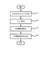
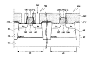
図1は、本発明の第1実施形態による半導体装置の製造方法を説明するためのフローチャートであり、図2Aないし図2Dは、本発明の第1実施形態による半導体装置の製造方法を説明するための断面図である。 FIG. 1 is a flowchart for explaining a semiconductor device manufacturing method according to a first embodiment of the present invention, and FIGS. 2A to 2D are diagrams for explaining a semiconductor device manufacturing method according to a first embodiment of the present invention. FIG.
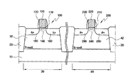
図1及び図2Aを参照すれば、半導体基板10上にNMOSトランジスタ100とPMOSトランジスタ200とを形成する(S10)。
Referring to FIGS. 1 and 2A, an
具体的に説明すれば、まず半導体基板10に素子分離領域20を形成して第1及び第2アクチブ領域30、40を定義する。ここで、半導体基板10は、シリコン基板、SOI(Silicon On Insulator)基板、ガリウム砒素基板、シリコンゲルマニウム基板、セラミックス基板、石英基板、またはディスプレイ用ガラス基板などになり、素子分離領域20はLOCOS(LOCal Oxidation of Silicon)方法を利用したFOX(Field OXide)またはSTI(Shallow Trench Isolation)になりうる。
More specifically, first, the
その後、第1アクチブ領域30にP型不純物を注入してPウェル32を形成し、第2アクチブ領域40にN型不純物を注入してNウェル42を形成する。
Thereafter, a P-type impurity is implanted into the first
引き続き、第1及び第2アクチブ領域30、40上に絶縁膜、導電膜を順次的に積層した後、パターニングして第1及び第2ゲート絶縁膜110、210、第1及び第2ゲート電極120、220を形成する。ここで、第1及び第2ゲート絶縁膜110、210は、SiO2、SiON、Si3N4、GexOyNz、GexSiyOz、高誘電率物質及びこれらの積層膜を使用することができる。ここで、高誘電率物質は、HfO2、ZrO2、Al2O3、Ta2O5、ハフニウムシリケート、ジルコニウムシリケートなどになりうる。また、第1及び第2ゲート電極120、220は、第1及び第2ゲート絶縁膜110上に各々形成され、例えば、ポリシリコン(poly Si)、不純物がイオン注入されたポリシリコン、ポリシリコンより抵抗の低い金属などを使うことができ、図面には表示しなかったが第1及び第2ゲート電極120、220の動作特性を向上させるためにポリシリコン上に金属または金属シリサイドをさらに形成できる。
Subsequently, an insulating film and a conductive film are sequentially stacked on the first and second
引き続き、スペーサ130、230を形成する。例えば、第1及び第2ゲート電極120、220を含む半導体基板10の全面にスペーサ用絶縁膜を順次的に形成した後、エッチバック(etch back)のような全面エッチング工程を用いて、第1及び第2ゲート電極120、220の側壁に各々スペーサ130、230を形成する。
Subsequently,
引き続き、N型及びP型ソース/ドレイン領域160、260を形成する。
Subsequently, N-type and P-type source /
具体的に、第2アクチブ領域40をマスクで遮断し、NMOSトランジスタ100の第1ゲート電極120、スペーサ130をイオン注入マスクとしてN型不純物、例えば砒素(As)を注入できる。第1アクチブ領域30をマスクで遮断し、PMOSトランジスタ200の第2ゲート電極220、スペーサ230をイオン注入マスクとしてP型不純物、例えば硼素(B)を注入できる。ここで、選択的に第1及び第2アクチブ領域30、40内に各々ハローイオン(halo ion)を注入できる。ハローイオンは、チャネル領域が短くなることによるパンチスルー現象を防止するためにゲート電極を形成した後、半導体基板のアクチブ領域の濃度を高めるために注入されるイオンを意味する。ハローイオンは、ソース/ドレイン領域を形成するために注入されるイオンと反対タイプのイオンとが主に使われる。したがって、第1アクチブ領域30内にはP型不純物、例えば硼素(B)を注入し、第2アクチブ領域40内にはN型不純物、例えば砒素(As)を注入できる。
Specifically, the second
本発明の第1実施形態によるNMOS及びPMOSトランジスタ100、200のソース/ドレイン領域160、260は多様な構造で変形可能であり、例えば、LDD(Lightly Diffused Drain)、DDD(Double Diffused Drain)、MIDDD(Mask Islanded Double Diffused Drain)、MLDD(Mask LDD)、LDMOS(Lateral Double-diffused MOS)構造などになりうる。
The source /
引き続き、イオン注入されたイオンを活性化させるか、格子損傷を回復させるために熱工程を実施できる。熱工程の方式は、RTP(Rapid Temperature Process)またはLSA(LaSer Annealing)などの方式を利用できる。 Subsequently, a thermal process can be performed to activate the implanted ions or to recover lattice damage. As a thermal process method, a method such as RTP (Rapid Temperature Process) or LSA (LaSer Annealing) can be used.
図1及び図2Bを参照すれば、NMOS及びPMOSトランジスタ100、200上に各々第1及び第2ライナ膜(liner layer)310、312を形成する(S20)。
Referring to FIGS. 1 and 2B, first and second liner layers 310 and 312 are formed on the NMOS and
具体的に、第1及び第2ライナ膜310、312は、例えば、SiN膜、SiON膜、LPCVD(Low Pressure Chemical Vapor Deposition)酸化膜、ALD(Atomic Layer Deposition)酸化膜、SOG(Spin On Glass)膜及びこれらの積層膜として、約50〜2000Åの厚さで形成することができる。
Specifically, the first and
このような第1及び第2ライナ膜310、312は、半導体装置1の製造工程の中に反射防止膜またはエッチング停止膜としての役割もし、所定ストレスを有する第1及び第2ライナ膜310、312をNMOS及びPMOSトランジスタ100、200上に形成することでNMOS及びPMOSトランジスタ100、200の動作特性が向上する。
The first and
具体的に、NMOSトランジスタ100上には所定の引張ストレスを有する第1ライナ膜310を形成し、PMOSトランジスタ200上には所定の圧縮ストレスを有する第2ライナ膜312を形成できる。例えば、第1及び第2ライナ膜310、312としてSiN膜を用いる場合、SiN膜はN-HボンディングとSi-Hボンディングの比率によって引張ストレスを与えるか、圧縮ストレスを与えるかが決定される。すなわち、N-Hボンディング/Si-Hボンディングの比率が約1〜5であれば引張ストレスを与え、約5〜20であれば圧縮ストレスを与える。したがって、本発明の第1実施形態で、第1ライナ膜310はN-Hボンディング/Si-Hボンディングの比率が約1〜5であるSiN膜を使って、第2ライナ膜312はN-Hボンディング/Si-Hボンディングの比率が約5〜20であるSiN膜を使うことができる。
Specifically, a
第1及び第2ライナ膜を形成する方法は、前述した方法に限定されず、例えばNMOS及びPMOSトランジスタ上に所定の引張ストレスを有するライナ膜を形成した後、PMOSトランジスタ上に形成されたライナ膜にはゲルマニウム及び/または窒素をイオン注入して引張ストレスを減少させることができる。 The method of forming the first and second liner films is not limited to the above-described method. For example, after forming a liner film having a predetermined tensile stress on the NMOS and PMOS transistors, the liner film formed on the PMOS transistors. Can be implanted with germanium and / or nitrogen to reduce tensile stress.
また、PMOSトランジスタ上に形成されたライナ膜にゲルマニウム及び/または窒素をイオン注入する工程を前述したように別途に進行せず、後述する工程(図6A参照)で第1層間絶縁膜(図6Aの320)にゲルマニウム及び/または窒素をイオン注入する工程で、ライナ膜と第1層間絶縁膜とを同時にイオン注入できる。 Further, as described above, the step of ion-implanting germanium and / or nitrogen into the liner film formed on the PMOS transistor does not proceed separately as described above, and the first interlayer insulating film (FIG. 6A) is formed in the step (see FIG. 6A) described later. 320), the liner film and the first interlayer insulating film can be simultaneously ion-implanted in the step of ion-implanting germanium and / or nitrogen.
それだけでなく、NMOS及びPMOSトランジスタ上に形成されたライナ膜の引張ストレスがPMOSトランジスタの動作特性を大きく低下させない場合、別途のイオン注入工程をしないこともある。 In addition, if the tensile stress of the liner film formed on the NMOS and PMOS transistors does not greatly deteriorate the operating characteristics of the PMOS transistor, a separate ion implantation process may not be performed.
図1及び図2Cを参照すれば、第1及び第2ライナ膜310、312上に所定のストレスを有する第1層間絶縁膜(ILD; Inter-Layer Dielectric)320を形成する(S30)。図面には表示しなかったが、第1層間絶縁膜320は半導体基板10上に形成されたNMOS及びPMOSトランジスタ100、200をメタル配線と接続するためのコンタクト(contact)を含むことができる。したがって、層間絶縁膜はメタル配線とメタル配線とを絶縁するためのメタル間絶縁膜(IMD; Inter-Metallic Dielectric)とは区別される。
1 and 2C, a first inter-layer dielectric (ILD) 320 having a predetermined stress is formed on the first and
具体的に、第1層間絶縁膜320は、O3-TEOS(O3-Tetra Ethyl Ortho Silicate)、USG(Undoped Silicate Glass)、PSG(Phospho Silicate Glass)、BSG(Borosilicate Glass)、BPSG(Boro Phospho Silicate Glass)、FSG(Fluoride Silicate Glass)、SOG(Spin On Glass)、TOSZ(Tonen Sila Zene)またはこれらの組合わせを使うことができる。本発明の第1実施形態では、第1層間絶縁膜320として所定の引張ストレス(tensile stress)を有するO3-TEOSを使った場合を例として説明する。ここで、第1層間絶縁膜320は、CVD(Chemical Vapor Deposition)方式、スピンコーティング方式などを用いて形成できる。
Specifically, the first
引き続き、以後工程の容易性のために選択的に、第1層間絶縁膜320を平坦化することもできる。
Subsequently, the first
図1及び図2Dを参照すれば、第1層間絶縁膜320を脱水素化してストレスを変化させる(S40)。 Referring to FIGS. 1 and 2D, the stress is changed by dehydrogenating the first interlayer insulating layer 320 (S40).
具体的に、第1層間絶縁膜320を脱水素化(水素イオンを除去(depletion))すれば、脱水素化された第1層間絶縁膜320内にボイド(void)が形成され、このようなボイドはストレスを変化させる。
Specifically, if the first
第1層間絶縁膜320を脱水素化ガス雰囲気でプラズマ処理、UV処理及び/または熱処理して脱水素化させることができる。図2Dでは、プラズマ処理400した場合を例示的に図示した。脱水素化ガスとしては、N2、O2、O3、N2O、H2及び/またはD2を含みうる。O3プラズマ処理の場合を例とすれば、工程温度は常温(room temperature)〜700℃、工程圧力は約10mTorr〜720Torrであり、RFパワー(RF power)は約20〜10000Wで調節できる。N2プラズマ処理、 N2Oプラズマ処理も類似した工程条件で進行させることができる。また、O3熱処理の場合を例とすれば、工程温度が約200〜700℃で熱処理を進行することができる。このようにプラズマ処理によって脱水素化されることについては実験例1に基づいて詳しく後述する。
The first
例えば、第1層間絶縁膜320としてO3-TEOSを使って脱水素化ガス雰囲気でプラズマ処理、UV処理及び/または熱処理して脱水素化すれば、脱水素化された第1層間絶縁膜320内のSi-OHボンディングなどが減る。このように水素イオンが減れば、脱水素化された第1層間絶縁膜320内にボイドが形成され、このようなボイドは引張ストレスを増加させる。工程条件によって異なるが、脱水素化の前に、O3-TEOS膜の引張ストレスは約10〜100MPaであり、脱水素化の後にはO3-TEOS膜の引張ストレスは約200MPa以上になりうる。
For example, if dehydrogenation is performed by using plasma treatment, UV treatment and / or heat treatment in a dehydrogenation gas atmosphere using O 3 -TEOS as the first
また、脱水素化ガス雰囲気でのプラズマ処理、UV処理及び/または熱処理は多数回連続的に(sequentially)進行しうる。例えば、第1層間絶縁膜320をO3プラズマ処理し、引き続きN2プラズマ処理できる。また、第1層間絶縁膜320をO3プラズマ処理し、引き続きN2熱処理することもできる。
In addition, plasma treatment, UV treatment, and / or heat treatment in a dehydrogenation gas atmosphere may proceed sequentially many times. For example, the first
以下では、図2Dを参照して、本発明の第1実施形態による半導体装置を説明する。 Hereinafter, the semiconductor device according to the first embodiment of the present invention will be described with reference to FIG. 2D.
本発明の第1実施形態による半導体装置1は、NMOSトランジスタ100上に脱水素化された第1層間絶縁膜320が形成されているので、NMOSトランジスタの電流駆動能力が増加する。
In the
具体的に、第1層間絶縁膜320の引張ストレスが増加すれば、第1層間絶縁膜320下部の第1ライナ膜と当接しているNMOSトランジスタ100のソース/ドレイン領域160に圧縮ストレスが発生し、ソース/ドレイン領域160に隣接したチャネル領域146には引張ストレスが発生する。このようにチャネル領域146に引張ストレスが発生すれば、チャネル領域146で電子の有効質量が減少し、電子の移動度(mobility)が増加するのでNMOSトランジスタ100の電流駆動能力が増加する。
Specifically, if the tensile stress of the first
例えば、第1層間絶縁膜320としてHDP(High Density Plasma)酸化膜を使う場合と、脱水素化されたO3-TEOS膜を使う場合とを比べて説明する。ここで、HDP膜は、ギャップフィル(gap-fill)特性に優れて第1ゲート電極120などによって発生した段差を易しく減らすことができ、従来の半導体装置で第1層間絶縁膜として主に使われた。HDP酸化膜は約-200MPaの圧縮ストレスを有し、脱水素化されたO3-TEOS膜は約200MPa以上の引張ストレスを有しうる。このようにストレス差がある場合、400MPaのストレス増加に比例してNMOSトランジスタ100は電流駆動能力は約10%以上増加しうる。但し、このような電流駆動能力の増加量は、NMOSトランジスタ100の特性(例えば、チャネルのサイズ、電子の濃度など)によって異なる。プラズマ処理によって引張ストレスが増加することについては実験例2に基づいて詳しく後述する。
For example, a case where an HDP (High Density Plasma) oxide film is used as the first
一方、所定厚さ以上の脱水素化された第1層間絶縁膜320は、NMOSトランジスタ100の電流駆動能力に影響を及ぼさない。
On the other hand, the dehydrogenated first
具体的に、NMOSトランジスタ100の第1ゲート絶縁膜110、第1ゲート電極120及びライナ膜310の総厚さをt1とし、ライナ膜310及び脱水素化された第1層間絶縁膜320の総厚さをt2とする時、t2/t11.14区間では脱水素化された第1層間絶縁膜320の厚さが増加するにつれて電子の移動度が比例して増加するが、t2/t1≧1.14区間では脱水素化された第1層間絶縁膜320の厚さが増加しても電子の移動度はそれ以上増加しない(飽和(saturation)状態になる)。したがって、第1層間絶縁膜320を脱水素化させてNMOSトランジスタ100の電流駆動能力を最大化させるためには、t2/t1≧1.14を満足しなければならない。このような結果については実験例3に基づいて詳しく後述する。
Specifically, the total thickness of the first
また、本発明の第1実施形態による半導体装置1は、脱水素化により第1層間絶縁膜320内に水素イオンの濃度が低いために、熱電子注入(hot electron injection)効果が減る。したがって、第1ゲート絶縁膜110の信頼性が向上する。
In addition, the
図3は、本発明の第2実施形態による半導体装置の製造方法を説明するための断面図である。図1ないし図2Cと実質的に同一の構成要素については同一の図面符号を付し、該当構成要素についての詳細な説明は省略する。 FIG. 3 is a cross-sectional view for explaining the method for manufacturing a semiconductor device according to the second embodiment of the present invention. Components that are substantially the same as those in FIGS. 1 to 2C are denoted by the same reference numerals, and detailed description of the corresponding components is omitted.
図3を参照すれば、本発明の第2実施形態による半導体装置2は、第1層間絶縁膜320を脱水素化した後(図1のS40)、脱水素化された第1層間絶縁膜320上への水分及び/または外部イオンの侵入を防止するキャッピング層330をさらに形成できる。
Referring to FIG. 3, in the
具体的に、脱水素化して第1層間絶縁膜320の引張ストレスの大きさを増加させても、多層の配線及び多層のメタル間の絶縁膜(Inter Metallic Dielectric ;IMD)を形成する後続工程中に水分及び/または外部イオンが第1層間絶縁膜320に侵入すれば、引張ストレスがまた小さくなりうる。例えば、第1層間絶縁膜320として使われるO3-TEOSは、後続工程中に吸湿される特性が強い。
Specifically, even if the tensile stress of the first
このような水分及び/または外部イオンは、第1ゲート絶縁膜110内に侵入してNMOSトランジスタ100のスレショルド(threshold voltage)の電圧レベルを変化させてドレインオフ電流(drain off current)を増加させるなど動作特性を低下させる。したがって、水分及び/または外部イオンの第1層間絶縁膜320への侵入を防止するためのキャッピング層330を形成できる。
Such moisture and / or external ions penetrate into the first
このようなキャッピング層330は、第1層間絶縁膜320を脱水素化した後、インサイチュ(in-situ)で進行して形成することがより効果的である。そして、キャッピング層330としては、HDP(High Density Plasma)酸化膜、PE-TEOS(Plasma Enhanced-Tetra Ethyl Ortho Silicate)などを使うことができる。
It is more effective to form the
図4は、本発明の第3実施形態による半導体装置の製造方法を説明するための断面図である。図1ないし図2Cと実質的に同一の構成要素については同一の図面符号を付し、該当構成要素についての詳細な説明は省略する。 FIG. 4 is a cross-sectional view for explaining the method for manufacturing a semiconductor device according to the third embodiment of the present invention. Components that are substantially the same as those in FIGS. 1 to 2C are denoted by the same reference numerals, and detailed description of the corresponding components is omitted.
図4を参照して、本発明の第3実施形態による半導体装置3は、第1層間絶縁膜320を脱水素化した後(図1のS40)、脱水素化された第1層間絶縁膜320上に脱水素化された追加層間絶縁膜340をさらに形成できる。
Referring to FIG. 4, in the
具体的に、第1層階間絶縁膜320上に所定のストレスを有する追加層間絶縁膜340を形成し、追加層間絶縁膜340を脱水素化してストレスを変化させる。
Specifically, an additional
追加層間絶縁膜340を脱水素化ガス雰囲気でプラズマ処理400及び/または熱処理して脱水素化させうる。図4では、プラズマ処理400した場合を例示的に図示した。追加層間絶縁膜340はO3-TEOS、USG、PSG、BSG、BPSG、FSG、SOG、TOSZなどが使用でき、例えば、CVD方式、スピンコーティング方式などを用いて形成できる。また、脱水素化ガスは例えば、N2、O2、O3、N2O、H2及び/またはD2を含みうる。脱水素化過程、例えば脱水素化ガス雰囲気でプラズマ処理、UV処理及び/または熱処理は、多数回連続的に(sequentially)進行しうる。
The additional
このように脱水素化された追加層間絶縁膜340は、引張ストレスが増加するので、NMOSトランジスタの電流駆動能力が増加する。
The additional
また、図面には表示しなかったが、追加層間絶縁膜340を形成し、形成された追加層間絶縁膜340を脱水素化する一連の過程を多数回繰り返して、NMOSトランジスタ100上に第1層間絶縁膜320と多層の追加層間絶縁膜340とを形成することができる。
Although not shown in the drawing, a series of processes of forming an additional
所定厚さ以上の脱水素化された追加層間絶縁膜340は、NMOSトランジスタの電流駆動能力に影響を及ぼさない。
The dehydrogenated additional
具体的に、NMOSトランジスタ100の第1ゲート絶縁膜110、第1ゲート電極120及びライナ膜310の総厚さをt1とし、ライナ膜310及び脱水素化された第1及び追加層間絶縁膜340の総厚さをt3とする時、t3/t11.14区間では脱水素化された第1層間絶縁膜320の厚さが増加するにつれて電子の移動度が比例して増加するが、t3/t1≧1.14区間では脱水素化された追加層間絶縁膜340の厚さが増加したり、多層の追加層間絶縁膜340が形成されても電子の移動度はそれ以上増加しない。したがって、追加層間絶縁膜340を脱水素化させ、NMOSトランジスタ100の電流駆動能力を最大化させるためには、t3/t1≧1.14を満足しなければならない。
Specifically, the total thickness of the first
図5は、本発明の第4実施形態による半導体装置の製造方法を説明するための断面図である。図1ないし図2Cと実質的に同一の構成要素については同一の図面符号を付し、該当構成要素についての詳細な説明は省略する。 FIG. 5 is a cross-sectional view for explaining the method for manufacturing a semiconductor device according to the fourth embodiment of the present invention. Components that are substantially the same as those in FIGS. 1 to 2C are denoted by the same reference numerals, and detailed description of the corresponding components is omitted.
図5を参照すれば、本発明の第4実施形態による半導体装置4は、第1層間絶縁膜320を脱水素化した後(図1のS40)、脱水素化された第1層間絶縁膜320上に第1層間絶縁膜320より小さなストレスを有する第2層間絶縁膜350をさらに形成できる。
Referring to FIG. 5, in the semiconductor device 4 according to the fourth embodiment of the present invention, after the first
具体的に、半導体装置は、NMOSトランジスタ100とメタルラインとの間のカップリングを防止するために層間絶縁膜を一定厚さ(t4)以上形成しなければならない。ところが、層間絶縁膜を一定厚さ(t4)以上形成した後、脱水素化して引張ストレスを増加させようとすれば、表面と近い層間絶縁膜の一部分は脱水素化が起きるが、ソース/ドレイン領域160と隣接した層間絶縁膜の一部分は脱水素化が起きないこともある。したがって、引張ストレスが十分に増加しないこともある。
Specifically, in the semiconductor device, in order to prevent coupling between the
したがって、NMOSトランジスタ100の第1ゲート絶縁膜110、第1ゲート電極120及びライナ膜310の総厚さをt1とし、ライナ膜310及び脱水素化された第1層間絶縁膜320の総厚さをt2とする時、t2/t1≧1.14区間を満足し、ソース/ドレイン領域160と隣接した第1層間絶縁膜の一部分も脱水素化が起きることができる厚さで第1層間絶縁膜320を形成できる。その後、第1層間絶縁膜320を脱水素化して、引張ストレスを増加させる。
Therefore, the total thickness of the first
その後、第1層間絶縁膜320上に所定厚さ(t4-t2)を有する第2層間絶縁膜350を形成できる。ここで、第2層間絶縁膜350は、厚さ(t2)以上で形成されるのでNMOSトランジスタ100の電流駆動能力に大きい影響を及ぼさないので、第2層間絶縁膜350が有するストレスの大きさに拘らず、層間絶縁膜を厚さ(t4)で形成できる。したがって、第2層間絶縁膜350は、第1層間絶縁膜320よりストレスの大きさが小さいことがある。すなわち、ストレスは、圧縮ストレスは負(-)の値であり、引張ストレスは正(+)であるので、第2層間絶縁膜350は第1層間絶縁膜320より小さな引張ストレスを有したり、圧縮ストレスを有してもよい。
Thereafter, a second
図6A及び図6Bは、本発明の第5及び第6実施形態による半導体装置の製造方法を説明するための断面図である。図1ないし図2Cと実質的に同一の構成要素については同一の図面符号を付し、該当構成要素についての詳細な説明は省略する。 6A and 6B are cross-sectional views for explaining a method of manufacturing a semiconductor device according to the fifth and sixth embodiments of the present invention. Components that are substantially the same as those in FIGS. 1 to 2C are denoted by the same reference numerals, and detailed description of the corresponding components is omitted.
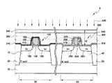
図6A及び図6Bを参照すれば、PMOSトランジスタ200のチャネル領域246には、圧縮ストレスを提供して初めて正孔移動度が向上する。ところが、本発明のように脱水素化された第1層間絶縁膜320は、PMOSトランジスタ200のチャネル領域246に引張ストレスを提供するので、PMOSトランジスタ200の電流駆動能力を落とすことがある。
Referring to FIGS. 6A and 6B, the hole mobility is improved only when a compressive stress is applied to the
本発明の第5実施形態による半導体装置5は、第1層間絶縁膜320を脱水素化した後(図1のS40参照)、図6AのようにNMOSトランジスタ100をカバーするマスクパターン350を用いてPMOSトランジスタ200上の脱水素化された第1層間絶縁膜320にゲルマニウム(Ge)及び/または窒素(N)をイオン注入410することによって、PMOSトランジスタ200上の脱水素化された第1層間絶縁膜320の引張ストレスを減らすことができる。
The semiconductor device 5 according to the fifth embodiment of the present invention uses the
本発明の第6実施形態による半導体装置6は、第1層間絶縁膜320を脱水素化する前に(図1のS40参照)、図6BのようにPMOSトランジスタ200をカバーするマスクパターン352を先に形成する。その後、第1層間絶縁膜320を脱水素化(例えば、脱水素化ガス雰囲気でプラズマ処理404)して、NMOSトランジスタ100上の第1層間絶縁膜320にのみ引張ストレスを与えることができる。
In the
このような方式により、PMOSトランジスタ200の電流駆動特性も維持できる。
With such a method, the current drive characteristics of the
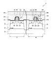
以下、図7及び図8Aないし図8Eを参照して、本発明の第7実施形態による半導体装置の製造方法を説明する。図7は、本発明の第7実施形態による半導体装置の製造方法を説明するためのフローチャートであり、図8Aないし図8Eは、本発明の第7実施形態による半導体装置の製造方法を説明するための断面図である。 Hereinafter, a method for fabricating a semiconductor device according to the seventh embodiment of the present invention will be described with reference to FIGS. 7 and 8A to 8E. FIG. 7 is a flowchart for explaining a method of manufacturing a semiconductor device according to a seventh embodiment of the present invention. FIGS. 8A to 8E are diagrams for explaining a method of manufacturing a semiconductor device according to the seventh embodiment of the present invention. FIG.
図8Aないし図8Cによる本発明の第7実施形態による半導体装置の製造方法は、図2Aないし図2Cと実質的に同一なので詳細な説明は省略する。 The method of manufacturing the semiconductor device according to the seventh embodiment of the present invention according to FIGS. 8A to 8C is substantially the same as FIGS.
これにより、図7及び図8Aないし図8Cによる半導体装置の製造方法を簡単に説明すれば、NMOS及びPMOSトランジスタ100、200を形成し(S100)、NMOS及びPMOSトランジスタ100、200上に各々第1及び第2ライナ膜310、312を形成する(S200)。そして、第1及び第2ライナ膜310、312上に所定のストレスを有する第1層間絶縁膜320を形成する(S300)。
7 and 8A to 8C, the NMOS and
以後、図7、図8D及び図8Eを参照して、第1層間絶縁膜320内にNMOS及びPMOSトランジスタ100、200をメタル配線と接続するためのコンタクト(contact)328を形成する(S400)。したがって、第1層間絶縁膜320は、メタル配線とメタル配線とを絶縁するためのメタル間絶縁膜(IMD; Inter-Metallic Dielectric)とは区別される。
Thereafter, referring to FIGS. 7, 8D and 8E, a
より詳細に説明すれば、図8Dに図示されたように第1層間絶縁膜320上にコンタクトホール(contact hole)322を形成するためのフォトレジストパターン(図示せず)を形成する。以後、フォトレジストパターン(図示せず)をエッチングマスクとしてゲート電極120、220及びソース/ドレイン領域160、260が露出されるまで第1層間絶縁膜320を部分エッチングしてコンタクトホール322を形成する。すなわち、各コンタクトホール322によってゲート電極120、220及び/またはソース/ドレイン領域160、260の表面が露出される。
More specifically, a photoresist pattern (not shown) for forming a
その後、図8Eに図示されたように、コンタクトホール322内に埋め込まれたコンタクト328を形成する。ここで、コンタクト328は、コンタクトホールに沿ってコンフォーマルに形成されたバリア膜324と金属膜326とからなる。
Thereafter, as shown in FIG. 8E, a
バリア膜(barrier layer)324は、コンタクトホール322内に埋め立てされる金属膜の接触性を向上させるためのオーミック膜(adhesion)と金属物質が拡散されてシリコンと反応することを防止する拡散防止膜(diffusion barrier)を形成して完成する。このとき、オーミック膜は、TiまたはTaなどのような高融点金属(refractory metal)をコンタクトホールの表面に沿ってコンフォーマルに蒸着して形成することができ、拡散防止膜はオーミック膜の表面に沿ってTiNまたはTaNなどを蒸着して形成できる。
The
以後、内壁にバリア膜324が形成されたコンタクトホール322内に金属物質を埋め込んでコンタクト328を完成する。ここで、コンタクト328は、コンタクトホール322内にW、CuまたはAlなどのような金属物質を蒸着して形成できる。
Thereafter, a metal material is buried in the
引き続き、第1層間絶縁膜320の表面が露出されるまでCMP(Chemical Mechanical Polishing)またはエッチバック(etch back)などのような平坦化工程を実施できる。
Subsequently, a planarization process such as CMP (Chemical Mechanical Polishing) or etch back can be performed until the surface of the first
その後、図7及び図8Eを参照して、第1層間絶縁膜320を脱水素化させることでストレスを変化させる(S500)。 7 and 8E, the stress is changed by dehydrogenating the first interlayer insulating film 320 (S500).
より詳細に説明すれば、第1層間絶縁膜320内の水素イオンを除去する脱水素化工程を行うことで第1層間絶縁膜320内にボイド(void)が形成され、ボイドがストレスを変化させる。
More specifically, voids are formed in the first
第1層間絶縁膜320を脱水素化する方法としては、脱水素化ガス雰囲気でプラズマ処理、UV処理及び/または熱処理などの方法がある。そして、脱水素化ガスとしては、N2、O2、O3、N2O、H2及び/またはD2を含みうる。
As a method for dehydrogenating the first
例えば、第1層間絶縁膜320としてO3-TEOSを使って、脱水素化ガス雰囲気でプラズマ処理、UV処理及び/または熱処理して脱水素化すれば、脱水素化された第1層間絶縁膜320内のSi-OHボンディングなどが減る。このように水素イオンが減れば、脱水素化された第1層間絶縁膜320内にボイドが形成され、このようなボイドは引張ストレスを増加させる。工程条件によって異なるが、脱水素化の前に、O3-TEOS膜の引張ストレスは約10〜100MPaであり、脱水素化の後にはO3-TEOS膜の引張ストレスは約200MPa以上になりうる。
For example, if O 3 -TEOS is used as the first
また、脱水素化ガス雰囲気でのプラズマ処理、UV処理及び/または熱処理は多数回連続的に(sequentially)進行することができる。例えば、第1層間絶縁膜320をO3プラズマ処理し、引き続きN2プラズマ処理できる。また、第1層間絶縁膜320をO3プラズマ処理して引き続きN2熱処理することもできる。
In addition, plasma treatment, UV treatment and / or heat treatment in a dehydrogenation gas atmosphere can proceed sequentially many times. For example, the first
このように、第1層間絶縁膜320内にコンタクト328を形成し、第1層間絶縁膜320を脱水素化させることによって、コンタクト形成時に、第1層間絶縁膜320のストレスが減少したり、第1層間絶縁膜320への水分の侵透を防止できる。
As described above, by forming the
以下では、図8Eを参照して、本発明の第7実施形態による半導体装置について説明する。 The semiconductor device according to the seventh embodiment of the present invention will be described below with reference to FIG. 8E.
本発明の第7実施形態による半導体装置7は、NMOSトランジスタ100上に脱水素化された第1層間絶縁膜320が形成されているので、NMOSトランジスタの電流駆動能力が増加する。
In the
具体的に、第1層間絶縁膜320の引張ストレスが増加すれば、第1層間絶縁膜320下部の第1ライナ膜と当接しているNMOSトランジスタ100のソース/ドレイン領域160に圧縮ストレスが発生し、ソース/ドレイン領域160に隣接したチャネル領域146には引張ストレスが発生する。このようにチャネル領域146に引張ストレスが発生すれば、チャネル領域146での有効質量が減少して電子の移動度(mobility)が増加するのでNMOSトランジスタ100の電流駆動能力が増加する。
Specifically, if the tensile stress of the first
以下、図9を参照して、本発明の第8実施形態による半導体装置について詳しく説明する。図9は、本発明の第8実施形態による半導体装置を説明するための断面図である。図8Aないし図8Cと実質的に同一の構成要素については同一の図面符号を付し、該当構成要素についての詳細な説明は省略する。 Hereinafter, the semiconductor device according to the eighth embodiment of the present invention will be described in detail with reference to FIG. FIG. 9 is a cross-sectional view for explaining a semiconductor device according to an eighth embodiment of the present invention. Components substantially the same as those in FIGS. 8A to 8C are denoted by the same reference numerals, and detailed description of the corresponding components is omitted.
図9を参照すれば、本発明の第8実施形態による半導体装置8は、第1層間絶縁膜320内にコンタクト328を形成した後、第1層間絶縁膜320を脱水素化し、第1層間絶縁膜320上の水分及び/または外部イオンの侵入を防止するキャッピング層330をさらに形成できる。
Referring to FIG. 9, in the semiconductor device 8 according to the eighth embodiment of the present invention, after the
具体的に、脱水素化して第1層間絶縁膜320の引張ストレスの大きさを増加させても、多層の配線及び多層のメタル間絶縁膜(Inter Metallic Dielectric; IMD)を形成する後続工程中に水分及び/または外部イオンが第1層間絶縁膜320に侵入すれば、引張ストレスが再び小さくなりうる。例えば、第1層間絶縁膜320として使われるO3-TEOSは、後続工程中に吸湿される特性が強い。
Specifically, even if the tensile stress of the first
このような水分及び/または外部イオンは、第1ゲート絶縁膜110内に侵入してNMOSトランジスタ100のスレショルド(threshold voltage)の電圧レベルを変化させてドレインオフ電流(drain off current)を増加させるなど動作特性を低下させうる。したがって、水分及び/または外部イオンの第1層間絶縁膜320への侵入を防止するためのキャッピング層330を形成できる。
Such moisture and / or external ions penetrate into the first
このようなキャッピング層330は、第1層間絶縁膜320を脱水素化した後、インサイチュ(in-situ)で進行して形成することがより効果的である。このようなキャッピング層330としては、HDP(High Density Plasma)酸化膜、PE-TEOS(Plasma Enhanced-Tetra Ethyl Ortho Silicate)またはSiN、SiONなどを使うことができる。
It is more effective to form the
以上、添付された図面を参照して、本発明の実施形態を説明したが、当業者ならば本発明がその技術的思想や必須な特徴を変更せず、他の具体的な形態で実施されるということを理解できるであろう。したがって、前述した実施形態は、あらゆる面で例示的なものであり、限定的ではないということを理解しなければならない。 The embodiments of the present invention have been described above with reference to the accompanying drawings. However, those skilled in the art can implement the present invention in other specific forms without changing the technical idea and essential features thereof. You will understand that. Accordingly, it should be understood that the above-described embodiments are illustrative in all aspects and not limiting.
本発明に関するより詳細な内容は、次の具体的な実験例を通じて説明し、ここに記載していない内容はこの技術分野で熟練された者なら十分に技術的に類推できるものなので説明を省略する。 More detailed contents regarding the present invention will be described through the following specific experimental examples, and contents not described here will be omitted because they can be sufficiently technically analogized by those skilled in the art. .
<実験例1>
NMOSトランジスタ上に所定引張ストレスを有するライナ膜を形成し、ライナ膜上に第1層間絶縁膜としてO3-TEOS膜を形成した後、第1層間絶縁膜をFT-IR(Fourier Transform-Infrared Spectrometers)を用いて成分を分析した。引き続き、NMOSトランジスタ上に形成された第1層間絶縁膜をO3プラズマ処理した後、第1層間絶縁膜のFT-IRを用いて成分を分析した。その結果が図10に図示されている。
<Experimental example 1>
A liner film having a predetermined tensile stress is formed on the NMOS transistor, and an O 3 -TEOS film is formed on the liner film as a first interlayer insulating film. ) Was used to analyze the components. Subsequently, the first interlayer insulating film formed on the NMOS transistor was subjected to O 3 plasma treatment, and then the components were analyzed using FT-IR of the first interlayer insulating film. The result is shown in FIG.
図10のx軸は波長(cm-1)であり、y軸は吸収度(absorbance)を表わす。FT-IRは、分子中に赤外線(infrared)を照射して分子内原子間の結合構造による固有な震動エネルギ領域の波長(約4000〜400cm-1の範囲)を吸収した後また放出するが、このような変化を測定して成分を分析する。図面符号aはO3プラズマ処理する前の結果であり、図面符号bはO3プラズマ処理した後の結果を表わす。aとbとを比べると、OH(H2O、Si-OH)と、Si-OHピーク(peak)が低くなったことが分かる。したがって、第1層間絶縁膜をO3プラズマ処理すれば、水素イオンの濃度が低くなることが分かる。 The x-axis in FIG. 10 represents the wavelength (cm −1 ), and the y-axis represents the absorbance. FT-IR emits infrared light into the molecule and absorbs the wavelength (in the range of about 4000 to 400 cm -1 ) of the intrinsic vibration energy region due to the bond structure between the atoms in the molecule. Components are analyzed by measuring such changes. The drawing symbol a represents the result before the O 3 plasma treatment, and the drawing symbol b represents the result after the O 3 plasma treatment. When a and b are compared, it can be seen that the OH (H 2 O, Si—OH) and the Si—OH peak are lowered. Therefore, it can be seen that the hydrogen ion concentration decreases when the first interlayer insulating film is treated with O 3 plasma.
<実験例2>
第1ないし第4NMOSトランジスタ上に所定引張ストレスを有するライナ膜を形成し、ライナ膜上に第1層間絶縁膜としてO3-TEOS膜を形成した後、第1層間絶縁膜のストレス大きさを各々測定した(As-Depo)。引き続き、第1ないし第4NMOSトランジスタ上に形成された第1層間絶縁膜を各々NH3プラズマ処理、O3プラズマ処理、N2プラズマ処理、O3プラズマ処理後、N2プラズマ処理して、第1層間絶縁膜のストレス大きさを各々測定した(Treatment)。その結果が、図11にともに図示されている。
<Experimental example 2>
A liner film having a predetermined tensile stress is formed on the first to fourth NMOS transistors, an O 3 -TEOS film is formed as a first interlayer insulating film on the liner film, and then the stress magnitude of the first interlayer insulating film is set respectively. Measured (As-Depo). Subsequently, the first interlayer insulating film formed on the first to fourth NMOS transistors is subjected to NH 3 plasma treatment, O 3 plasma treatment, N 2 plasma treatment, O 3 plasma treatment, and N 2 plasma treatment, respectively. Each of the stress levels of the interlayer insulating film was measured (Treatment). The result is shown together in FIG.
図11のx軸はプラズマ処理の種類を表わし、y軸は引張ストレスの大きさを表わす。NH3プラズマ処理は、第1層間絶縁膜内の水素イオンを除去するのに効果的ではないので、NH3プラズマ処理前後の引張ストレスの増加が微々たることが分かる。一方、O3プラズマ処理、N2プラズマ処理、O3プラズマ処理後、N2プラズマ処理した場合、処理の前には約10MPaであったが、処理後には各々約210MPa、330MPa、370MPaに増加したことが分かる。すなわち、O3プラズマ処理、N2プラズマ処理などは、第1層間絶縁膜内の水素イオンを除去するのに効果的であることが分かる。 The x-axis in FIG. 11 represents the type of plasma treatment, and the y-axis represents the magnitude of tensile stress. Since NH 3 plasma treatment is not effective in removing hydrogen ions in the first interlayer insulating film, it can be seen that there is a slight increase in tensile stress before and after NH 3 plasma treatment. On the other hand, after O 3 plasma treatment, N 2 plasma treatment, O 3 plasma treatment, and N 2 plasma treatment, it was about 10 MPa before treatment, but increased to about 210 MPa, 330 MPa, and 370 MPa after treatment, respectively. I understand that. That is, it can be seen that O 3 plasma treatment, N 2 plasma treatment, and the like are effective in removing hydrogen ions in the first interlayer insulating film.
<実験例3>
シミュレーションプログラムにNMOSトランジスタ上に所定の引張ストレスを有するライナ膜を位置し、ライナ膜上に所定の引張ストレスを有した第1層間絶縁膜が位置するように設定した。その後、第1層間絶縁膜の厚さを変更させながら、それによる電子の移動度変化(mobility change)をシミュレーションした。その結果が、図12に図示されている。
<Experimental example 3>
In the simulation program, the liner film having a predetermined tensile stress was positioned on the NMOS transistor, and the first interlayer insulating film having the predetermined tensile stress was positioned on the liner film. After that, while changing the thickness of the first interlayer insulating film, the mobility change of the electrons was simulated. The result is illustrated in FIG.
図12のx軸はt2/t1(但し、t1は、NMOSトランジスタのゲート絶縁膜、ゲート電極及びライナ膜の総厚さ、t2は、ライナ膜及び脱水素化された第1層間絶縁膜の総厚さ)であり、y軸は標準化された電子の移動度変化である。t2/t1≧1.14で電子の移動度がそれ以上増加しないことが分かる。したがって、第1層間絶縁膜を脱水素化させ、NMOSトランジスタの電流駆動能力を最大化させるためにはt2/t1≧1.14を満足しなければならないことが分かる。 In FIG. 12, the x-axis is t2 / t1 (where t1 is the total thickness of the gate insulating film, gate electrode, and liner film of the NMOS transistor, and t2 is the total thickness of the liner film and the dehydrogenated first interlayer insulating film. Thickness), and the y-axis is the standardized electron mobility change. It can be seen that the electron mobility does not increase any more at t2 / t1 ≧ 1.14. Therefore, it is understood that t2 / t1 ≧ 1.14 must be satisfied in order to dehydrogenate the first interlayer insulating film and maximize the current drive capability of the NMOS transistor.
動作特性を向上させるための半導体装置及びその製造方法に適用されうる。 The present invention can be applied to a semiconductor device for improving operating characteristics and a manufacturing method thereof.
1 半導体装置
10 半導体基板
20 素子分離領域
30 第1アクチブ領域
32 Pウェル
40 第2アクチブ領域
42 Nウェル
100 NMOSトランジスタ
110 第1ゲート絶縁膜
120 第1ゲート電極
130 スペーサ
146 チャネル領域
160 ソース/ドレイン領域
200 PMOSトランジスタ
210 第2ゲート絶縁膜
220 第2ゲート電極
230 スペーサ
246 チャネル領域
260 ソース/ドレイン領域
310 第1ライナ膜
312 第2ライナ膜
320 第1層間絶縁膜
400 プラズマ処理
DESCRIPTION OF
Claims (8)
前記NMOSトランジスタ上に引張ストレスを有するライナ膜を形成する工程と、
前記ライナ膜上に第1層間絶縁膜を形成する工程と、
前記第1層間絶縁膜を脱水素化する工程とを含み、
前記NMOSトランジスタは、ゲート絶縁膜及びゲート電極を含み、前記ゲート絶縁膜、前記ゲート電極及び前記ライナ膜の総厚さをt1とし、前記ライナ膜及び前記第1層間絶縁膜の総厚さをt2とする時、t2/t1≧ 1.14であることを特徴とする半導体装置の製造方法。 Forming an NMOS transistor on the substrate;
Forming a liner film having tensile stress on the NMOS transistor;
Forming a first interlayer insulating film on the liner film ;
Look including a step of dehydrogenating the first interlayer insulating film,
The NMOS transistor includes a gate insulating film and a gate electrode. The total thickness of the gate insulating film, the gate electrode, and the liner film is t1, and the total thickness of the liner film and the first interlayer insulating film is t2. Where t2 / t1 ≧ 1.14 . A method for manufacturing a semiconductor device, wherein
Applications Claiming Priority (4)
| Application Number | Priority Date | Filing Date | Title |
|---|---|---|---|
| KR10-2005-0106096 | 2005-11-07 | ||
| KR1020050106096A KR100678636B1 (en) | 2005-11-07 | 2005-11-07 | Fabricating method for semiconductor integrated circuit device and semiconductor integrated circuit device fabricated by the same |
| KR1020060073912A KR100834737B1 (en) | 2006-08-04 | 2006-08-04 | Fabricating method for semiconductor integrated circuit device and semiconductor integrated circuit device fabricated by the same |
| KR10-2006-0073912 | 2006-08-04 |
Publications (3)
| Publication Number | Publication Date |
|---|---|
| JP2007134712A JP2007134712A (en) | 2007-05-31 |
| JP2007134712A5 JP2007134712A5 (en) | 2009-12-24 |
| JP5209196B2 true JP5209196B2 (en) | 2013-06-12 |
Family
ID=38004288
Family Applications (1)
| Application Number | Title | Priority Date | Filing Date |
|---|---|---|---|
| JP2006301719A Active JP5209196B2 (en) | 2005-11-07 | 2006-11-07 | Manufacturing method of semiconductor device |
Country Status (3)
| Country | Link |
|---|---|
| US (2) | US7867867B2 (en) |
| JP (1) | JP5209196B2 (en) |
| TW (1) | TWI338335B (en) |
Families Citing this family (24)
| Publication number | Priority date | Publication date | Assignee | Title |
|---|---|---|---|---|
| JP2007324391A (en) * | 2006-06-01 | 2007-12-13 | Matsushita Electric Ind Co Ltd | Semiconductor device and its manufacturing method |
| DE102006030264B4 (en) * | 2006-06-30 | 2008-08-28 | Advanced Micro Devices, Inc., Sunnyvale | A method of fabricating transistors having a biaxially-deformed channel caused by silicon germanium in the gate electrode |
| US20080138983A1 (en) * | 2006-12-06 | 2008-06-12 | Taiwan Semiconductor Manufacturing Co., Ltd. | Method of forming tensile stress films for NFET performance enhancement |
| US20080206943A1 (en) * | 2007-02-26 | 2008-08-28 | Jei-Ming Chen | Method of forming strained cmos transistor |
| JP2008235636A (en) * | 2007-03-22 | 2008-10-02 | Elpida Memory Inc | Method of manufacturing semiconductor device, and semiconductor device |
| US7741171B2 (en) * | 2007-05-15 | 2010-06-22 | Taiwan Semiconductor Manufacturing Company, Ltd. | Oxygen-rich layers underlying BPSG |
| JP5280716B2 (en) * | 2007-06-11 | 2013-09-04 | ルネサスエレクトロニクス株式会社 | Semiconductor device and manufacturing method thereof |
| US8072035B2 (en) | 2007-06-11 | 2011-12-06 | Renesas Electronics Corporation | Semiconductor device and method of manufacturing the same |
| US7911001B2 (en) | 2007-07-15 | 2011-03-22 | Samsung Electronics Co., Ltd. | Methods for forming self-aligned dual stress liners for CMOS semiconductor devices |
| US7858532B2 (en) * | 2007-08-06 | 2010-12-28 | United Microelectronics Corp. | Dielectric layer structure and manufacturing method thereof |
| US8466508B2 (en) * | 2007-10-03 | 2013-06-18 | Macronix International Co., Ltd. | Non-volatile memory structure including stress material between stacked patterns |
| DE102007057686B4 (en) * | 2007-11-30 | 2011-07-28 | GLOBALFOUNDRIES Dresden Module One Ltd. Liability Company & Co. KG, 01109 | A method and semiconductor device having a protective layer for reducing stress relaxation in a dual stress coating technique |
| US8211784B2 (en) * | 2009-10-26 | 2012-07-03 | Advanced Ion Beam Technology, Inc. | Method for manufacturing a semiconductor device with less leakage current induced by carbon implant |
| JP5652939B2 (en) * | 2010-07-07 | 2015-01-14 | ルネサスエレクトロニクス株式会社 | Semiconductor device and manufacturing method of semiconductor device |
| CN102569083B (en) * | 2010-12-23 | 2014-12-24 | 中芯国际集成电路制造(上海)有限公司 | Method for forming metal-oxide semiconductor with high potassium (K) metal gate |
| US8853862B2 (en) * | 2011-12-20 | 2014-10-07 | International Business Machines Corporation | Contact structures for semiconductor transistors |
| US9177803B2 (en) * | 2013-03-14 | 2015-11-03 | Globalfoundries Inc. | HK/MG process flows for P-type semiconductor devices |
| US9252271B2 (en) * | 2013-11-27 | 2016-02-02 | Taiwan Semiconductor Manufacturing Company Limited | Semiconductor device and method of making |
| KR102292813B1 (en) * | 2015-10-14 | 2021-08-23 | 삼성전자주식회사 | Semiconductor device and method for fabricating the same |
| US10020401B2 (en) * | 2016-11-29 | 2018-07-10 | Taiwan Semiconductor Manufacturing Company, Ltd. | Methods for straining a transistor gate through interlayer dielectric (ILD) doping schemes |
| FR3076077B1 (en) * | 2017-12-22 | 2020-02-28 | Commissariat A L'energie Atomique Et Aux Energies Alternatives | CONSTRUCTION OF CONSTRAINED CHANNEL TRANSISTORS |
| US11881522B2 (en) | 2018-10-05 | 2024-01-23 | Semiconductor Energy Laboratory Co., Ltd. | Semiconductor device and manufacturing method of semiconductor device |
| CN109686663A (en) * | 2018-12-27 | 2019-04-26 | 上海华力微电子有限公司 | A kind of semiconductor structure and its manufacturing method |
| KR20210153385A (en) | 2020-06-10 | 2021-12-17 | 삼성전자주식회사 | Integrated circuit devices |
Family Cites Families (20)
| Publication number | Priority date | Publication date | Assignee | Title |
|---|---|---|---|---|
| JPS5730337A (en) * | 1980-07-30 | 1982-02-18 | Nec Corp | Formation of surface protecting film for semiconductor |
| JP2885458B2 (en) * | 1990-02-27 | 1999-04-26 | 株式会社東芝 | Thin film transistor |
| JPH04345069A (en) * | 1991-05-22 | 1992-12-01 | Oki Electric Ind Co Ltd | Semiconductor device |
| JP2758847B2 (en) * | 1995-02-08 | 1998-05-28 | 日本電気株式会社 | Method of forming spin-on-glass film |
| KR100289194B1 (en) | 1996-06-29 | 2001-05-02 | 이구택 | Method for recycling furnace sludge with a converter scrap |
| JPH10173075A (en) | 1996-12-05 | 1998-06-26 | Sanyo Electric Co Ltd | Manufacture of semiconductor device and manufacture of semiconductor memory device |
| JP3745863B2 (en) | 1997-02-28 | 2006-02-15 | 芝浦メカトロニクス株式会社 | Wet etching processing method and processing apparatus therefor |
| JP2000164716A (en) * | 1998-11-26 | 2000-06-16 | Seiko Epson Corp | Semiconductor device and manufacture thereof |
| JP3562357B2 (en) * | 1998-12-22 | 2004-09-08 | セイコーエプソン株式会社 | Method for manufacturing semiconductor device |
| TW473800B (en) | 1999-12-28 | 2002-01-21 | Semiconductor Energy Lab | Method of manufacturing a semiconductor device |
| JP2001250956A (en) * | 2000-03-08 | 2001-09-14 | Semiconductor Energy Lab Co Ltd | Semiconductor device |
| AU2001267880A1 (en) * | 2000-11-22 | 2002-06-03 | Hitachi Ltd. | Semiconductor device and method for fabricating the same |
| KR100391992B1 (en) | 2000-12-08 | 2003-07-22 | 삼성전자주식회사 | METHOD OF FORMING SEMICONDUCTOR DEVICES HAVING SiOC LAYER |
| JP4557508B2 (en) | 2003-06-16 | 2010-10-06 | パナソニック株式会社 | Semiconductor device |
| TWI235458B (en) | 2003-07-02 | 2005-07-01 | Taiwan Semiconductor Mfg | MOS transistor and fabrication method thereof |
| JP4683833B2 (en) * | 2003-10-31 | 2011-05-18 | 株式会社半導体エネルギー研究所 | Functional circuit and design method thereof |
| JP4322687B2 (en) * | 2004-01-09 | 2009-09-02 | エルピーダメモリ株式会社 | Manufacturing method of semiconductor device |
| US20050186722A1 (en) * | 2004-02-25 | 2005-08-25 | Kuan-Lun Cheng | Method and structure for CMOS device with stress relaxed by ion implantation of carbon or oxygen containing ions |
| KR101025761B1 (en) * | 2004-03-30 | 2011-04-04 | 삼성전자주식회사 | Semiconductor Integrated circuit and method of manufacturing the same |
| DE102004026149B4 (en) * | 2004-05-28 | 2008-06-26 | Advanced Micro Devices, Inc., Sunnyvale | A method of producing a semiconductor device having transistor elements with voltage-inducing etch stop layers |
-
2006
- 2006-11-07 TW TW095141118A patent/TWI338335B/en active
- 2006-11-07 JP JP2006301719A patent/JP5209196B2/en active Active
- 2006-11-07 US US11/593,898 patent/US7867867B2/en active Active
-
2011
- 2011-01-10 US US12/987,415 patent/US8237202B2/en active Active
Also Published As
| Publication number | Publication date |
|---|---|
| TWI338335B (en) | 2011-03-01 |
| US20110163386A1 (en) | 2011-07-07 |
| US8237202B2 (en) | 2012-08-07 |
| JP2007134712A (en) | 2007-05-31 |
| US20070105297A1 (en) | 2007-05-10 |
| US7867867B2 (en) | 2011-01-11 |
| TW200729353A (en) | 2007-08-01 |
Similar Documents
| Publication | Publication Date | Title |
|---|---|---|
| JP5209196B2 (en) | Manufacturing method of semiconductor device | |
| US7534678B2 (en) | Methods of forming CMOS integrated circuit devices having stressed NMOS and PMOS channel regions therein and circuits formed thereby | |
| US7888214B2 (en) | Selective stress relaxation of contact etch stop layer through layout design | |
| US8384167B2 (en) | Semiconductor device with field effect transistor and manufacturing method thereof | |
| US8084787B2 (en) | PMD liner nitride films and fabrication methods for improved NMOS performance | |
| US20120252198A1 (en) | Method for manufacturing semiconductor structure | |
| US20070200185A1 (en) | Semiconductor device and method for fabricating the same | |
| US6184114B1 (en) | MOS transistor formation | |
| US20080206943A1 (en) | Method of forming strained cmos transistor | |
| US20190295847A1 (en) | Transistor | |
| US7714364B2 (en) | Semiconductor device comprising gate electrode having arsenic and phosphorus | |
| US7192822B2 (en) | Method of fabricating CMOS type semiconductor device having dual gates | |
| US7618857B2 (en) | Method of reducing detrimental STI-induced stress in MOSFET channels | |
| US7172936B2 (en) | Method to selectively strain NMOS devices using a cap poly layer | |
| KR100678636B1 (en) | Fabricating method for semiconductor integrated circuit device and semiconductor integrated circuit device fabricated by the same | |
| KR100834737B1 (en) | Fabricating method for semiconductor integrated circuit device and semiconductor integrated circuit device fabricated by the same | |
| US8470656B2 (en) | Semiconductor device and method of manufacturing the same | |
| KR100724574B1 (en) | Semiconductor device having etch stop layer and fabricating method thereof | |
| JP2011165973A (en) | Semiconductor device and method for manufacturing the same | |
| US20050142784A1 (en) | Methods of fabricating semiconductor devices | |
| US20070200151A1 (en) | Semiconductor device and method of fabricating the same | |
| KR100744248B1 (en) | Method for forming semiconductor device | |
| KR20050065229A (en) | Method for fabricating the mos transistor | |
| US20020155674A1 (en) | Method for preventing boron penentration of a MOS transistor | |
| JP2005347631A (en) | Semiconductor device and method for manufacturing the same |
Legal Events
| Date | Code | Title | Description |
|---|---|---|---|
| A521 | Request for written amendment filed |
Free format text: JAPANESE INTERMEDIATE CODE: A523 Effective date: 20091106 |
|
| A621 | Written request for application examination |
Free format text: JAPANESE INTERMEDIATE CODE: A621 Effective date: 20091106 |
|
| A521 | Request for written amendment filed |
Free format text: JAPANESE INTERMEDIATE CODE: A523 Effective date: 20101026 |
|
| A977 | Report on retrieval |
Free format text: JAPANESE INTERMEDIATE CODE: A971007 Effective date: 20120911 |
|
| A131 | Notification of reasons for refusal |
Free format text: JAPANESE INTERMEDIATE CODE: A131 Effective date: 20120918 |
|
| A521 | Request for written amendment filed |
Free format text: JAPANESE INTERMEDIATE CODE: A523 Effective date: 20121217 |
|
| TRDD | Decision of grant or rejection written | ||
| A01 | Written decision to grant a patent or to grant a registration (utility model) |
Free format text: JAPANESE INTERMEDIATE CODE: A01 Effective date: 20130212 |
|
| A61 | First payment of annual fees (during grant procedure) |
Free format text: JAPANESE INTERMEDIATE CODE: A61 Effective date: 20130221 |
|
| FPAY | Renewal fee payment (event date is renewal date of database) |
Free format text: PAYMENT UNTIL: 20160301 Year of fee payment: 3 |
|
| R150 | Certificate of patent or registration of utility model |
Free format text: JAPANESE INTERMEDIATE CODE: R150 Ref document number: 5209196 Country of ref document: JP Free format text: JAPANESE INTERMEDIATE CODE: R150 |
|
| R250 | Receipt of annual fees |
Free format text: JAPANESE INTERMEDIATE CODE: R250 |
|
| R250 | Receipt of annual fees |
Free format text: JAPANESE INTERMEDIATE CODE: R250 |
|
| R250 | Receipt of annual fees |
Free format text: JAPANESE INTERMEDIATE CODE: R250 |
|
| R250 | Receipt of annual fees |
Free format text: JAPANESE INTERMEDIATE CODE: R250 |
|
| R250 | Receipt of annual fees |
Free format text: JAPANESE INTERMEDIATE CODE: R250 |
|
| R250 | Receipt of annual fees |
Free format text: JAPANESE INTERMEDIATE CODE: R250 |
|
| R250 | Receipt of annual fees |
Free format text: JAPANESE INTERMEDIATE CODE: R250 |
|
| R250 | Receipt of annual fees |
Free format text: JAPANESE INTERMEDIATE CODE: R250 |
|
| R250 | Receipt of annual fees |
Free format text: JAPANESE INTERMEDIATE CODE: R250 |