JP5152352B2 - Liquid crystal display substrate and liquid crystal display device - Google Patents
Liquid crystal display substrate and liquid crystal display device Download PDFInfo
- Publication number
- JP5152352B2 JP5152352B2 JP2011019833A JP2011019833A JP5152352B2 JP 5152352 B2 JP5152352 B2 JP 5152352B2 JP 2011019833 A JP2011019833 A JP 2011019833A JP 2011019833 A JP2011019833 A JP 2011019833A JP 5152352 B2 JP5152352 B2 JP 5152352B2
- Authority
- JP
- Japan
- Prior art keywords
- liquid crystal
- crystal display
- pattern
- pixel
- display device
- Prior art date
- Legal status (The legal status is an assumption and is not a legal conclusion. Google has not performed a legal analysis and makes no representation as to the accuracy of the status listed.)
- Expired - Fee Related
Links
Images


Classifications
-
- G—PHYSICS
- G02—OPTICS
- G02F—OPTICAL DEVICES OR ARRANGEMENTS FOR THE CONTROL OF LIGHT BY MODIFICATION OF THE OPTICAL PROPERTIES OF THE MEDIA OF THE ELEMENTS INVOLVED THEREIN; NON-LINEAR OPTICS; FREQUENCY-CHANGING OF LIGHT; OPTICAL LOGIC ELEMENTS; OPTICAL ANALOGUE/DIGITAL CONVERTERS
- G02F1/00—Devices or arrangements for the control of the intensity, colour, phase, polarisation or direction of light arriving from an independent light source, e.g. switching, gating or modulating; Non-linear optics
- G02F1/01—Devices or arrangements for the control of the intensity, colour, phase, polarisation or direction of light arriving from an independent light source, e.g. switching, gating or modulating; Non-linear optics for the control of the intensity, phase, polarisation or colour
- G02F1/13—Devices or arrangements for the control of the intensity, colour, phase, polarisation or direction of light arriving from an independent light source, e.g. switching, gating or modulating; Non-linear optics for the control of the intensity, phase, polarisation or colour based on liquid crystals, e.g. single liquid crystal display cells
- G02F1/1323—Arrangements for providing a switchable viewing angle
-
- G—PHYSICS
- G02—OPTICS
- G02F—OPTICAL DEVICES OR ARRANGEMENTS FOR THE CONTROL OF LIGHT BY MODIFICATION OF THE OPTICAL PROPERTIES OF THE MEDIA OF THE ELEMENTS INVOLVED THEREIN; NON-LINEAR OPTICS; FREQUENCY-CHANGING OF LIGHT; OPTICAL LOGIC ELEMENTS; OPTICAL ANALOGUE/DIGITAL CONVERTERS
- G02F1/00—Devices or arrangements for the control of the intensity, colour, phase, polarisation or direction of light arriving from an independent light source, e.g. switching, gating or modulating; Non-linear optics
- G02F1/01—Devices or arrangements for the control of the intensity, colour, phase, polarisation or direction of light arriving from an independent light source, e.g. switching, gating or modulating; Non-linear optics for the control of the intensity, phase, polarisation or colour
- G02F1/13—Devices or arrangements for the control of the intensity, colour, phase, polarisation or direction of light arriving from an independent light source, e.g. switching, gating or modulating; Non-linear optics for the control of the intensity, phase, polarisation or colour based on liquid crystals, e.g. single liquid crystal display cells
- G02F1/133—Constructional arrangements; Operation of liquid crystal cells; Circuit arrangements
- G02F1/1333—Constructional arrangements; Manufacturing methods
- G02F1/1343—Electrodes
-
- G—PHYSICS
- G02—OPTICS
- G02F—OPTICAL DEVICES OR ARRANGEMENTS FOR THE CONTROL OF LIGHT BY MODIFICATION OF THE OPTICAL PROPERTIES OF THE MEDIA OF THE ELEMENTS INVOLVED THEREIN; NON-LINEAR OPTICS; FREQUENCY-CHANGING OF LIGHT; OPTICAL LOGIC ELEMENTS; OPTICAL ANALOGUE/DIGITAL CONVERTERS
- G02F1/00—Devices or arrangements for the control of the intensity, colour, phase, polarisation or direction of light arriving from an independent light source, e.g. switching, gating or modulating; Non-linear optics
- G02F1/01—Devices or arrangements for the control of the intensity, colour, phase, polarisation or direction of light arriving from an independent light source, e.g. switching, gating or modulating; Non-linear optics for the control of the intensity, phase, polarisation or colour
- G02F1/13—Devices or arrangements for the control of the intensity, colour, phase, polarisation or direction of light arriving from an independent light source, e.g. switching, gating or modulating; Non-linear optics for the control of the intensity, phase, polarisation or colour based on liquid crystals, e.g. single liquid crystal display cells
- G02F1/133—Constructional arrangements; Operation of liquid crystal cells; Circuit arrangements
- G02F1/1333—Constructional arrangements; Manufacturing methods
- G02F1/1335—Structural association of cells with optical devices, e.g. polarisers or reflectors
- G02F1/133509—Filters, e.g. light shielding masks
- G02F1/133512—Light shielding layers, e.g. black matrix
-
- G—PHYSICS
- G02—OPTICS
- G02F—OPTICAL DEVICES OR ARRANGEMENTS FOR THE CONTROL OF LIGHT BY MODIFICATION OF THE OPTICAL PROPERTIES OF THE MEDIA OF THE ELEMENTS INVOLVED THEREIN; NON-LINEAR OPTICS; FREQUENCY-CHANGING OF LIGHT; OPTICAL LOGIC ELEMENTS; OPTICAL ANALOGUE/DIGITAL CONVERTERS
- G02F1/00—Devices or arrangements for the control of the intensity, colour, phase, polarisation or direction of light arriving from an independent light source, e.g. switching, gating or modulating; Non-linear optics
- G02F1/01—Devices or arrangements for the control of the intensity, colour, phase, polarisation or direction of light arriving from an independent light source, e.g. switching, gating or modulating; Non-linear optics for the control of the intensity, phase, polarisation or colour
- G02F1/13—Devices or arrangements for the control of the intensity, colour, phase, polarisation or direction of light arriving from an independent light source, e.g. switching, gating or modulating; Non-linear optics for the control of the intensity, phase, polarisation or colour based on liquid crystals, e.g. single liquid crystal display cells
- G02F1/133—Constructional arrangements; Operation of liquid crystal cells; Circuit arrangements
- G02F1/1333—Constructional arrangements; Manufacturing methods
- G02F1/1337—Surface-induced orientation of the liquid crystal molecules, e.g. by alignment layers
- G02F1/133707—Structures for producing distorted electric fields, e.g. bumps, protrusions, recesses, slits in pixel electrodes
-
- G—PHYSICS
- G02—OPTICS
- G02F—OPTICAL DEVICES OR ARRANGEMENTS FOR THE CONTROL OF LIGHT BY MODIFICATION OF THE OPTICAL PROPERTIES OF THE MEDIA OF THE ELEMENTS INVOLVED THEREIN; NON-LINEAR OPTICS; FREQUENCY-CHANGING OF LIGHT; OPTICAL LOGIC ELEMENTS; OPTICAL ANALOGUE/DIGITAL CONVERTERS
- G02F1/00—Devices or arrangements for the control of the intensity, colour, phase, polarisation or direction of light arriving from an independent light source, e.g. switching, gating or modulating; Non-linear optics
- G02F1/01—Devices or arrangements for the control of the intensity, colour, phase, polarisation or direction of light arriving from an independent light source, e.g. switching, gating or modulating; Non-linear optics for the control of the intensity, phase, polarisation or colour
- G02F1/13—Devices or arrangements for the control of the intensity, colour, phase, polarisation or direction of light arriving from an independent light source, e.g. switching, gating or modulating; Non-linear optics for the control of the intensity, phase, polarisation or colour based on liquid crystals, e.g. single liquid crystal display cells
- G02F1/133—Constructional arrangements; Operation of liquid crystal cells; Circuit arrangements
- G02F1/136—Liquid crystal cells structurally associated with a semi-conducting layer or substrate, e.g. cells forming part of an integrated circuit
- G02F1/1362—Active matrix addressed cells
- G02F1/1368—Active matrix addressed cells in which the switching element is a three-electrode device
-
- G—PHYSICS
- G02—OPTICS
- G02F—OPTICAL DEVICES OR ARRANGEMENTS FOR THE CONTROL OF LIGHT BY MODIFICATION OF THE OPTICAL PROPERTIES OF THE MEDIA OF THE ELEMENTS INVOLVED THEREIN; NON-LINEAR OPTICS; FREQUENCY-CHANGING OF LIGHT; OPTICAL LOGIC ELEMENTS; OPTICAL ANALOGUE/DIGITAL CONVERTERS
- G02F1/00—Devices or arrangements for the control of the intensity, colour, phase, polarisation or direction of light arriving from an independent light source, e.g. switching, gating or modulating; Non-linear optics
- G02F1/01—Devices or arrangements for the control of the intensity, colour, phase, polarisation or direction of light arriving from an independent light source, e.g. switching, gating or modulating; Non-linear optics for the control of the intensity, phase, polarisation or colour
- G02F1/13—Devices or arrangements for the control of the intensity, colour, phase, polarisation or direction of light arriving from an independent light source, e.g. switching, gating or modulating; Non-linear optics for the control of the intensity, phase, polarisation or colour based on liquid crystals, e.g. single liquid crystal display cells
- G02F1/133—Constructional arrangements; Operation of liquid crystal cells; Circuit arrangements
- G02F1/1333—Constructional arrangements; Manufacturing methods
- G02F1/1335—Structural association of cells with optical devices, e.g. polarisers or reflectors
- G02F1/133509—Filters, e.g. light shielding masks
- G02F1/133514—Colour filters
-
- G—PHYSICS
- G02—OPTICS
- G02F—OPTICAL DEVICES OR ARRANGEMENTS FOR THE CONTROL OF LIGHT BY MODIFICATION OF THE OPTICAL PROPERTIES OF THE MEDIA OF THE ELEMENTS INVOLVED THEREIN; NON-LINEAR OPTICS; FREQUENCY-CHANGING OF LIGHT; OPTICAL LOGIC ELEMENTS; OPTICAL ANALOGUE/DIGITAL CONVERTERS
- G02F1/00—Devices or arrangements for the control of the intensity, colour, phase, polarisation or direction of light arriving from an independent light source, e.g. switching, gating or modulating; Non-linear optics
- G02F1/01—Devices or arrangements for the control of the intensity, colour, phase, polarisation or direction of light arriving from an independent light source, e.g. switching, gating or modulating; Non-linear optics for the control of the intensity, phase, polarisation or colour
- G02F1/13—Devices or arrangements for the control of the intensity, colour, phase, polarisation or direction of light arriving from an independent light source, e.g. switching, gating or modulating; Non-linear optics for the control of the intensity, phase, polarisation or colour based on liquid crystals, e.g. single liquid crystal display cells
- G02F1/133—Constructional arrangements; Operation of liquid crystal cells; Circuit arrangements
- G02F1/1333—Constructional arrangements; Manufacturing methods
- G02F1/1343—Electrodes
- G02F1/134309—Electrodes characterised by their geometrical arrangement
- G02F1/134336—Matrix
-
- G—PHYSICS
- G02—OPTICS
- G02F—OPTICAL DEVICES OR ARRANGEMENTS FOR THE CONTROL OF LIGHT BY MODIFICATION OF THE OPTICAL PROPERTIES OF THE MEDIA OF THE ELEMENTS INVOLVED THEREIN; NON-LINEAR OPTICS; FREQUENCY-CHANGING OF LIGHT; OPTICAL LOGIC ELEMENTS; OPTICAL ANALOGUE/DIGITAL CONVERTERS
- G02F1/00—Devices or arrangements for the control of the intensity, colour, phase, polarisation or direction of light arriving from an independent light source, e.g. switching, gating or modulating; Non-linear optics
- G02F1/01—Devices or arrangements for the control of the intensity, colour, phase, polarisation or direction of light arriving from an independent light source, e.g. switching, gating or modulating; Non-linear optics for the control of the intensity, phase, polarisation or colour
- G02F1/13—Devices or arrangements for the control of the intensity, colour, phase, polarisation or direction of light arriving from an independent light source, e.g. switching, gating or modulating; Non-linear optics for the control of the intensity, phase, polarisation or colour based on liquid crystals, e.g. single liquid crystal display cells
- G02F1/133—Constructional arrangements; Operation of liquid crystal cells; Circuit arrangements
- G02F1/1333—Constructional arrangements; Manufacturing methods
- G02F1/1343—Electrodes
- G02F1/134309—Electrodes characterised by their geometrical arrangement
- G02F1/134381—Hybrid switching mode, i.e. for applying an electric field with components parallel and orthogonal to the substrates
-
- G—PHYSICS
- G02—OPTICS
- G02F—OPTICAL DEVICES OR ARRANGEMENTS FOR THE CONTROL OF LIGHT BY MODIFICATION OF THE OPTICAL PROPERTIES OF THE MEDIA OF THE ELEMENTS INVOLVED THEREIN; NON-LINEAR OPTICS; FREQUENCY-CHANGING OF LIGHT; OPTICAL LOGIC ELEMENTS; OPTICAL ANALOGUE/DIGITAL CONVERTERS
- G02F1/00—Devices or arrangements for the control of the intensity, colour, phase, polarisation or direction of light arriving from an independent light source, e.g. switching, gating or modulating; Non-linear optics
- G02F1/01—Devices or arrangements for the control of the intensity, colour, phase, polarisation or direction of light arriving from an independent light source, e.g. switching, gating or modulating; Non-linear optics for the control of the intensity, phase, polarisation or colour
- G02F1/13—Devices or arrangements for the control of the intensity, colour, phase, polarisation or direction of light arriving from an independent light source, e.g. switching, gating or modulating; Non-linear optics for the control of the intensity, phase, polarisation or colour based on liquid crystals, e.g. single liquid crystal display cells
- G02F1/137—Devices or arrangements for the control of the intensity, colour, phase, polarisation or direction of light arriving from an independent light source, e.g. switching, gating or modulating; Non-linear optics for the control of the intensity, phase, polarisation or colour based on liquid crystals, e.g. single liquid crystal display cells characterised by the electro-optical or magneto-optical effect, e.g. field-induced phase transition, orientation effect, guest-host interaction or dynamic scattering
- G02F1/139—Devices or arrangements for the control of the intensity, colour, phase, polarisation or direction of light arriving from an independent light source, e.g. switching, gating or modulating; Non-linear optics for the control of the intensity, phase, polarisation or colour based on liquid crystals, e.g. single liquid crystal display cells characterised by the electro-optical or magneto-optical effect, e.g. field-induced phase transition, orientation effect, guest-host interaction or dynamic scattering based on orientation effects in which the liquid crystal remains transparent
-
- G—PHYSICS
- G02—OPTICS
- G02F—OPTICAL DEVICES OR ARRANGEMENTS FOR THE CONTROL OF LIGHT BY MODIFICATION OF THE OPTICAL PROPERTIES OF THE MEDIA OF THE ELEMENTS INVOLVED THEREIN; NON-LINEAR OPTICS; FREQUENCY-CHANGING OF LIGHT; OPTICAL LOGIC ELEMENTS; OPTICAL ANALOGUE/DIGITAL CONVERTERS
- G02F2203/00—Function characteristic
- G02F2203/64—Normally black display, i.e. the off state being black
Abstract
Description
本発明は、液晶表示用基板及びこの基板を備えた液晶表示装置に関する。 The present invention relates to a liquid crystal display substrate and a liquid crystal display device including the substrate.
近年、液晶表示装置を用いた電子機器の軽量化が進み、携帯電話、モバイルPCなどのような情報機器が、公共の場で使用される機会が増加している。公共の場で情報機器を使用すると、液晶表示装置に表示された機密情報又はプライベート情報が、周辺の他者に視認される可能性がある。 In recent years, electronic devices using a liquid crystal display device have been reduced in weight, and information devices such as mobile phones and mobile PCs have been increasingly used in public places. When an information device is used in a public place, there is a possibility that confidential information or private information displayed on the liquid crystal display device will be visually recognized by others in the vicinity.
公共の場で液晶表示装置に機密情報又はプライベート情報を表示させる場合には、液晶表示装置は狭い視野となり、液晶表示装置に表示される情報を複数の者が見る場合には、液晶表示装置は広い視野となることが好ましい。視野制御の方式には、概ね2方式がある。 When displaying confidential information or private information on a liquid crystal display device in a public place, the liquid crystal display device has a narrow field of view, and when multiple people view information displayed on the liquid crystal display device, the liquid crystal display device It is preferable to have a wide field of view. There are roughly two types of visual field control methods.
第1の視野制御方式は、特許文献1(特許第3322197号公報)及び特許文献2(特許第4367206号公報)に開示されている。この第1の視野制御方式では、主たる表示を行う液晶表示素子と、広視野と狭視野とを切り替える視野角制御用液晶素子との2枚の液晶パネルが用いられる。特許文献1では、視野角制御用液晶素子が位相差制御用素子であり、この位相差制御用素子に印可する電圧の有無で広視野と狭視野を切り替える。特許文献2は、視野角制御用液晶素子に明るい領域と暗い領域のチェッカーフラグ・パターンを形成し、表示用液晶表示装置の表示を見づらくさせる技術である。特許文献1及び特許文献2は、いずれも視野角制御用液晶素子を配設することが必要で表示装置全体が厚くかつ重くなり、実用的でない場合がある。表示装置が厚くかつ重くなると、携帯電話、モバイルPCなどの携帯用個人端末の利便性は低下する。
The 1st visual field control system is indicated by patent documents 1 (patent 3322197 gazette) and patent documents 2 (patent 4367206 gazette). In the first visual field control method, two liquid crystal panels are used, which are a liquid crystal display element that performs main display and a viewing angle control liquid crystal element that switches between a wide visual field and a narrow visual field. In Patent Document 1, the viewing angle control liquid crystal element is a phase difference control element, and the wide field and the narrow field are switched depending on the presence or absence of a voltage applied to the phase difference control element. Japanese Patent Application Laid-Open No. 2004-228561 is a technique that makes it difficult to see the display of a liquid crystal display device for display by forming checker flag patterns of bright and dark regions on a viewing angle control liquid crystal element. In both Patent Document 1 and
第2の視野制御方式として、1枚の表示用液晶表示素子の画素に新たに視野角制御用画素を加える、又は、表示用画素の一部に視野角制御用領域を設ける方式がある。この第2の視野制御方式は、視野角制御用液晶素子を付加することが不必要なため、携帯用表示機器に適している。視野角制御用画素を加える方式の一例として、特許文献3(特開2010−128126号公報)が挙げられる。特許文献3では、視野角制御用サブ画素が視野角制御に用いられる。視野角制御用領域を設ける方式の一例として、特許文献4(特開2007−65046号公報)が挙げられる。特許文献4では、一画素内に第1の対向電極と第2の対向電極が設けられており、薄膜トランジスタと接続される第1の対向電極と第2の対向電極との間で、異なる対向電圧が印加され、第2の対向電極が視野角制御に用いられる。視野角制御用画素を用いる場合、及び対向電極が別形成された視野角制御領域を設ける場合においては、実効的な表示面積は減少し、表示が暗くなる場合がある。視野角制御用画素又は視野角制御領域を採用することにより、表示内容は周囲の第三者に視認されにくくはなる。しかしながら、観察者(液晶表示装置の使用者)であっても、視野角制御用画素又は視野角制御領域の光が目に入りやすいため、表示品質が低下する場合がある。加えて、特許文献4に示される技術は、2種の対向電圧が必要で電源系が複雑になる。また、特許文献4では、高コントラストの液晶表示装置に適用されるVA(垂直配向:Vertically Alignment)液晶又はECB(Electrically Changed Birefringence)液晶について検討されていない。
As a second visual field control method, there is a method in which a viewing angle control pixel is newly added to a pixel of one display liquid crystal display element or a viewing angle control region is provided in a part of the display pixel. This second visual field control method is suitable for portable display devices because it is unnecessary to add a liquid crystal element for controlling the visual field angle. As an example of a method of adding a viewing angle control pixel, Japanese Patent Application Laid-Open No. 2010-128126 is cited. In
通常のVA方式又はECB方式などの液晶表示装置は、共通電極を備えたカラーフィルタ基板と、液晶を駆動する複数の画素電極(例えば、薄膜トランジスタ(TFT)素子と電気的に接続され、櫛歯状パターン状に形成された透明電極)を備えたアレイ基板とで、液晶を挟持する基本的構成を持つ。この構成では、カラーフィルタ上の共通電極とアレイ基板側に形成された画素電極との間に駆動電圧が印加され、液晶が駆動される。画素電極及びカラーフィルタ表面の共通電極に用いられる透明導電膜は、通常、ITO(Indium Tin Oxide)、IZO(Indium Zinc Oxide)、IGZO(Indium Garium Zinc Oxide)などの導電性の金属酸化物の薄膜が用いられる。 A liquid crystal display device such as a normal VA method or ECB method is electrically connected to a color filter substrate having a common electrode and a plurality of pixel electrodes (for example, thin film transistor (TFT) elements) that drive liquid crystal, and has a comb shape. It has a basic structure for sandwiching liquid crystal with an array substrate provided with a transparent electrode formed in a pattern. In this configuration, a driving voltage is applied between the common electrode on the color filter and the pixel electrode formed on the array substrate side, and the liquid crystal is driven. The transparent conductive film used for the pixel electrode and the common electrode on the color filter surface is usually a conductive metal oxide thin film such as ITO (Indium Tin Oxide), IZO (Indium Zinc Oxide), and IGZO (Indium Garium Zinc Oxide). Is used.
上述したように、従来の視野角制御においては、余分な視野角制御用液晶素子を備えることによって液晶表示装置が重くかつ厚くなる場合がある。 As described above, in the conventional viewing angle control, the liquid crystal display device may be heavy and thick by providing an extra viewing angle control liquid crystal element.
また、従来の視野角制御においては、視野角制御用画素を備えることにより、実効的な開口率が低下する場合がある。 In the conventional viewing angle control, the effective aperture ratio may be reduced by providing the viewing angle control pixels.
本発明は、以上のような事情に鑑みてなされており、液晶表示装置が重くかつ厚くなることを防止し、開口率が低下することを防止し、効果的な視野角制御を行うための液晶表示用基板、及びこれを具備する液晶表示装置を提供することを目的とする。 The present invention has been made in view of the above circumstances, and a liquid crystal for preventing the liquid crystal display device from becoming heavy and thick, preventing the aperture ratio from being lowered, and performing effective viewing angle control. It is an object to provide a display substrate and a liquid crystal display device including the same.
第1の態様において、液晶表示用基板は、液晶表示装置に用いられる。液晶表示装置は、液晶表示用基板と、当該液晶表示用基板に液晶層を挟んで対向し、かつ、メタル配線を備えたアレイ基板とを具備する。液晶表示用基板は、多角形画素又は多角形サブピクセルと、線状パターンとを具備する。多角形画素又は多角形サブピクセルは、平面形状において向かい合い、かつ、メタル配線と平行な辺を持つ。線状パターンは、多角形画素又は多角形サブピクセルの向かい合う平行な辺に備えられ、基板面の垂直方向で前記メタル配線と対向し、斜め光を透過する。 In the first aspect, the liquid crystal display substrate is used in a liquid crystal display device. The liquid crystal display device includes a liquid crystal display substrate and an array substrate that faces the liquid crystal display substrate with a liquid crystal layer interposed therebetween and includes metal wiring. The liquid crystal display substrate includes polygonal pixels or polygonal subpixels and a linear pattern. Polygonal pixel or polygonal sub-pixel have opposite case in a planar shape, and has a metal wire and parallel sides. The linear pattern is provided on parallel sides facing each other of the polygon pixel or the polygon sub-pixel, and is opposed to the metal wiring in the direction perpendicular to the substrate surface and transmits oblique light.
第2の態様において、液晶表示装置は、液晶表示用基板と、当該液晶表示用基板に液晶層を挟んで対向し、かつ、メタル配線を備えたアレイ基板とを具備する。液晶表示用基板は、平面形状において向かい合い、かつ、メタル配線と平行な辺を持つ多角形画素又は多角形サブピクセルと、多角形画素又は多角形サブピクセルの向かい合う平行な辺に備えられ、基板面の垂直方向でメタル配線と対向し、斜め光を透過する線状パターンとを具備する。アレイ基板は、液晶層の液晶を駆動するアクティブ素子を備える。
In a second aspect, a liquid crystal display device includes a liquid crystal display substrate and an array substrate that is opposed to the liquid crystal display substrate with a liquid crystal layer interposed therebetween and includes metal wiring . Liquid crystal display substrate is had opposite case in a planar shape, and a polygonal pixel or polygonal sub-pixel having a metal wiring and parallel sides, provided in parallel sides facing the polygonal pixel or polygonal sub-pixel, A linear pattern that opposes the metal wiring in the direction perpendicular to the substrate surface and transmits oblique light is provided. The array substrate includes an active element for driving the liquid crystal of the liquid crystal layer.
本発明によれば、視野角制御において液晶表示装置が重くかつ厚くなることを防止することができ、開口率が低下することを防止することができ、効果的な視野角制御を行うことができる。 ADVANTAGE OF THE INVENTION According to this invention, it can prevent that a liquid crystal display device becomes heavy and thick in viewing angle control, can prevent that an aperture ratio falls, and can perform effective viewing angle control. .
以下、図面を参照しながら本発明の実施形態について説明する。なお、以下の説明において、同一又は実質的に同一の機能及び構成要素については、同一符号を付し、必要に応じて説明を行う。 Hereinafter, embodiments of the present invention will be described with reference to the drawings. In the following description, the same or substantially the same functions and components are denoted by the same reference numerals, and will be described as necessary.
(第1の実施形態)
本実施形態においては、初期垂直配向の液晶又は初期水平配向の液晶を備えるノーマリーブラックの液晶表示装置について説明する。本実施形態においては、サブピクセル単位の構成について説明するが、本実施形態と同様の構成を画素単位に適用してもよい。
(First embodiment)
In the present embodiment, a normally black liquid crystal display device having an initial vertical alignment liquid crystal or an initial horizontal alignment liquid crystal will be described. In the present embodiment, the configuration in units of subpixels will be described, but the same configuration as in this embodiment may be applied in units of pixels.
図1は、本実施形態に係る液晶表示装置の一例を示す部分断面図である。この図1は、櫛歯状の電極の櫛歯軸に垂直な断面である。図1では、液晶表示用基板2及びアレイ基板3による液晶L1〜L14の動作と、この動作によって実現される斜め光8とが図示されている。この図1において、垂直配向膜、偏光板、位相差板、TFTについては、図示することを省略している。
FIG. 1 is a partial cross-sectional view showing an example of a liquid crystal display device according to the present embodiment. FIG. 1 is a cross section perpendicular to the comb axis of the comb-like electrode. In FIG. 1, the operation of the liquid crystals L1 to L14 by the liquid
図2は、この図1のうち液晶表示用基板2の一例を示す部分断面図である。
FIG. 2 is a partial sectional view showing an example of the liquid
図3は、本実施形態に係る液晶表示用基板2の一例を示す部分平面図である。この図3におけるA−A’断面が、図1に相当する。
FIG. 3 is a partial plan view showing an example of the liquid
液晶表示装置1は、VA方式又はECB方式であるとする。ECB液晶としては、誘電率異方性が正の液晶を用いる。 The liquid crystal display device 1 is assumed to be a VA system or an ECB system. A liquid crystal having positive dielectric anisotropy is used as the ECB liquid crystal.
液晶表示装置1において、液晶表示用基板2と、TFTなどの液晶駆動素子(アクティブ素子)が形成されたアレイ基板3とは対向する。液晶表示用基板2とアレイ基板3との間には、液晶層4が挟持される。
In the liquid crystal display device 1, the liquid
マトリクス状に配置される多角形サブピクセルの開口部の平面視形状は、例えば、正方形、長方形、平行四辺形、くの字状に折れ曲がった(「V」字型、又は、ブーメラン型)多角形などのような、対向する辺が互いに平行な多角形である。図3の例において、液晶表示用基板2は、平面において複数の多角形サブピクセルを区切るマトリクスパターンの辺のうちの互いに向かい合う少なくとも2つの辺において、透明樹脂層の線状の透明パターン5が遮光層の線状の遮光パターン6で挟持された線状パターン7を具備する。液晶表示装置1では、透明パターン5を透過する斜め光8が、視野角制御に利用される。線状パターン7において、透明パターン5の垂直方向の厚さは、遮光パターン6の垂直方向の厚さよりも厚い。したがって、透明パターン5は、遮光パターン6よりも液晶層4側に突出している。さらに、液晶表示用基板2においては、線状パターン7の形成部分は、例えばカラーフィルタ10〜12の形成部分などのような他の部分より厚い。
The planar view shape of the openings of the polygonal subpixels arranged in a matrix is, for example, a square, a rectangle, a parallelogram, or a polygon that is bent in a dogleg shape ("V" shape or boomerang type). The polygons whose opposing sides are parallel to each other, such as In the example of FIG. 3, the liquid
本実施形態において、液晶層4はVA液晶であるとする。したがって、液晶層4の液晶L1〜L14は誘電率異方性が負の液晶である。液晶層4の液晶L1〜L14の初期配向は垂直である。図1において、透明パターン5と遮光パターン6との境界近傍の液晶L3,L4,L11,L12を除き、液晶L1,L2,L5〜L10,L13,L14は、液晶表示用基板2及びアレイ基板3の表面に垂直に配向している。本実施形態では、垂直配向膜が用いられるが、光配向及びラビングなどのような配向処理が省略可能である。後述されるように、本実施形態においては、従来のVA方式で必要であった89度などの厳密なチルト角制御が不要であり、例えば90度などのような単純な初期垂直配向の液晶を用いることができる。
In the present embodiment, it is assumed that the
初期垂直配向の液晶表示装置1は、初期水平配向の液晶表示装置と異なり、液晶表示装置1の両面又は片面に貼付される偏光板及び位相差板の光軸合わせが厳しくなくてもよい。初期垂直配向の液晶表示装置1において、電圧無印加時のリタデーションは、例えば0nmである。初期垂直配向の液晶表示装置1において、液晶と例えば偏光板の遅相軸とのズレが多少存在する場合であっても、光漏れは発生しにくく、ほぼ完全な黒表示を得ることができる。初期水平配向の液晶と偏光板との間で数度の光軸ずれがあると、光漏れが発生し、初期垂直配向の液晶より液晶表示装置のコントラストがやや劣化する場合がある。 The liquid crystal display device 1 with the initial vertical alignment is different from the liquid crystal display device with the initial horizontal alignment, and it is not necessary to strictly align the optical axes of the polarizing plate and the retardation plate attached to both surfaces or one surface of the liquid crystal display device 1. In the liquid crystal display device 1 with the initial vertical alignment, the retardation when no voltage is applied is, for example, 0 nm. In the liquid crystal display device 1 with the initial vertical alignment, even if there is a slight deviation between the liquid crystal and, for example, the slow axis of the polarizing plate, light leakage hardly occurs and almost complete black display can be obtained. If there is an optical axis misalignment of several degrees between the initially horizontal alignment liquid crystal and the polarizing plate, light leakage may occur, and the contrast of the liquid crystal display device may be slightly deteriorated compared to the initial vertical alignment liquid crystal.
本実施形態において、アレイ基板3は、多角形サブピクセルごとに、画素電極である第1電極P1〜P6と、共通電極である第2電極C1〜C6とを備えている。第1電極P1〜P6と、第2電極C1〜C6とには、液晶を駆動するために異なる電位が印加される。なお、アレイ基板3は、第2電極C1〜C6を備えなくてもよい。この場合、液晶表示装置は、第2電極C1〜C6を備えず、第1電極P1〜P6と、TFTなどのアクティブ素子とを備えるアレイ基板と、液晶表示用基板2とによって構成される。第2電極C1〜C6を省略した場合、第1電極P1〜P6の平面視形状は、櫛歯状パターン、又は、ベタ状の透明導電膜に複数のスリット状開口を形成したパターンとしてもよい。
In the present embodiment, the
図1及び図2の例において、ガラスなどの透明基板9の一方の表面上に線状パターン7が形成される。透明基板9、及び、透明パターン5とこの透明パターン5を挟む遮光パターン6とを具備する線状パターン7の上に、透明導電膜である第3電極13が配設される。次に、垂直方向において第3電極13の上であり、水平方向において線状パターン7の間(線状パターン7の形成されていない位置)に、それぞれ赤カラーフィルタ10、緑カラーフィルタ11、青カラーフィルタ12が備えられる。これにより、赤カラーフィルタ10、緑カラーフィルタ11、青カラーフィルタ12の端部に線状パターン7が備えられた構成が得られる。第3電極3、及び、赤カラーフィルタ10、緑カラーフィルタ11、青カラーフィルタ12の上に、必要に応じて、保護層7が積層される。
In the example of FIGS. 1 and 2, a
図3の例においては、赤カラーフィルタ10、緑カラーフィルタ11、青カラーフィルタ12と、線状パターン7との配置関係が示されている。本実施形態において、TFTなどのような液晶を駆動するアクティブ素子は、液晶表示装置1の平面と垂直な方向(厚み方向)において、線状パターン7の下部又は遮光パターン6の下部に配置される。図1及び図2の断面図では、液晶表示用基板2は、製造工程終了後に、180°回転させた状態となっている。液晶表示用基板2の製造工程では、透明基板9上に、線状パターン7が形成される。次に、透明基板9及び線状パターン7上に、第3電極13が形成される。次に、第3電極13の上であり線状パターン7の間に、赤カラーフィルタ10、緑カラーフィルタ11、青カラーフィルタ12が形成される。次に、赤カラーフィルタ10、緑カラーフィルタ11、青カラーフィルタ12、線状パターン7上の第3電極13の上に、必要に応じて、保護層7が積層される。
In the example of FIG. 3, the arrangement relationship between the
液晶表示用基板2の保護層7側は、液晶表示装置1の液晶層4側となる。液晶表示用基板2の透明基板9側は、観察者側となる。
The
本実施形態において、斜め光8は、透明パターン5を通る。この斜め光8により視野角制御が実現される。
In the present embodiment, the
アレイ基板3は、基板15、絶縁層16a〜16c、メタル配線17、第1電極P1〜P6、第2電極C1〜C6を具備する。
The
絶縁層16aは、基板15上に形成される。絶縁層16a上には、メタル配線17が形成される。メタル配線17は、液晶表示装置1の垂直方向において、線状パターン7と重なる位置に形成される。この構成により、垂直方向の光は、メタル配線17で遮光され、線状パターン7の透明パターン5から出射されることがない。絶縁層16a及びメタル配線17の上に、絶縁層16bが形成される。絶縁層16bの上に、第2電極C1〜C6が形成される。絶縁層16b及び第2電極C1〜C6の上に、絶縁層16cが形成される。絶縁層16cの上に、第1電極P1〜P6が形成される。
The insulating
図4は、本実施形態に係る液晶表示装置1の構成と斜め光8との関係の一例を示す部分断面図である。この図4では、説明を簡略化するために、サブピクセルの中心軸Zから左側のみを示している。さらに、この図4では、第1電極Pが矩形状の場合を例として示している。この図4において、垂直配向膜、偏光板、位相差板、TFTは、図示することを省略している。
FIG. 4 is a partial cross-sectional view showing an example of the relationship between the configuration of the liquid crystal display device 1 according to the present embodiment and the
アレイ基板3は、矩形状の第1電極Pと、この矩形状の第1電極Pと接続されているTFTとを備える。アレイ基板3の第1電極P1〜P6側と、液晶表示用基板2の保護層7側とは、液晶層4を介して向かい合う。
The
図4においては、液晶L1〜L6は、負の誘電率異方性を持つ。透明パターン5と遮光パターン6との境界近傍の液晶L3,L4を除き、液晶L1,L2,L5,L6は、液晶表示用基板2及びアレイ基板3の表面に垂直に配向している。なお、ECB方式では、配向膜をラビングし、正の誘電率異方性の液晶が水平に配向される。偏光板はクロスニコルであり、液晶表示装置1はノーマリーブラックとする。アレイ基板3には、信号線として用いることが可能なメタル配線17が、垂直方向において、線状パターン7と重なる位置に配置される。
In FIG. 4, the liquid crystals L1 to L6 have negative dielectric anisotropy. Except for the liquid crystals L3 and L4 in the vicinity of the boundary between the
なお、メタル配線17は、例えば、TFT製造で用いられる遮光性の金属薄膜をパターン形成することにより製造される。メタル配線17は、例えば、映像信号線、走査信号線、共通電極配線、あるいは、配向膜のラビング時のTFT素子の静電破壊防止に用いる共通導体配線などのうちのいずれでもよい。電気的なクロストーク及び不都合な寄生容量形成を避けるため、メタル配線17と第1電極Pとの間の垂直方向の距離を大きくしてもよい。
The
図4では、駆動電圧が無印加であり、液晶L1,L2,L5,L6が初期配向垂直である状態を示している。透明パターン5の表面に近い液晶L3は、若干斜めに配向している。斜め光8は、この液晶L3を斜めに横切る状態で透過する。斜め光8は、液晶L3と角度θを持つため、液晶L3は斜め光8に位相差を付与する。斜め光8は、図示していない偏光板を透過し、漏れ光として外部に出射される。この場合、透明パターン5は、観察者方向からは黒表示として視認されるが、斜め方向の第三者には漏れ光が観察され黒表示として視認されない。
FIG. 4 shows a state in which no drive voltage is applied and the liquid crystals L1, L2, L5, and L6 are perpendicular to the initial alignment. The liquid crystal L3 close to the surface of the
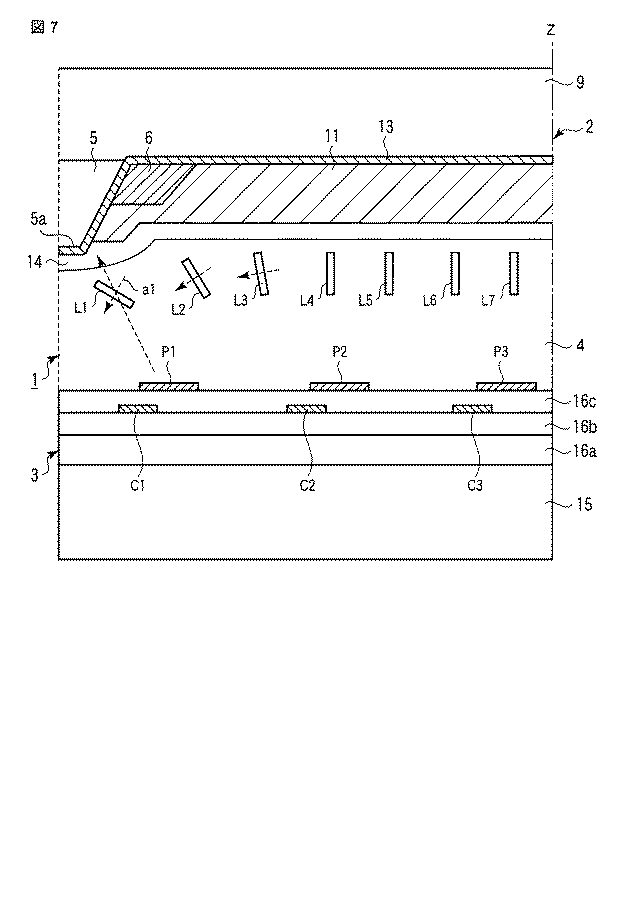
この漏れ光の量及び斜め光8の角度θは、透明パターン5の幅W1、線状パターン7の幅W2、透明パターン5の厚さH1、透明パターン5と保護層14との厚さHt、液晶層4の厚みLt、メタル配線17の幅W3、透明パターン5の表面に近い液晶L3のチルト角などで制御可能である。
The amount of leakage light and the angle θ of the
図5は、本実施形態に係る液晶表示装置1における透明パターン5の形状の変形例を示す部分断面図である。
FIG. 5 is a partial cross-sectional view showing a modification of the shape of the
透明パターン5の断面のうち、遮光パターン6、及び、カラーフィルタ10〜12よりも液晶層4側に突出している部分(透明パターン5の断面の先端部)5aの側辺は、先端に行くほど細くなるように傾斜していてもよい。なお、透明パターン5の突出部分5aは、丸みを持つとしてもよい。透明パターン5の突出部分5aの高さを調整することにより、液晶L3のチルト角と斜め光8の角度を合わせて漏れ光を少なくすることも可能である。透明パターン5と保護層14との厚さHt及び液晶層4の厚みLtを小さくした場合、又は、メタル配線17の幅W3を透明パターン5の幅W1より広くした場合には、斜め光8の角度θは大きくなる。ただし、角度θを大きくすると、斜め光8の強度が低下するため、厚みLt、幅W1の条件は、目的とする視野角制御の効果に合わせて適宜調整される。
Of the cross section of the
上述のように、斜め光8は、線状パターン7の突出部分(透明パターンの断面の頂部)5aを経由して出射される。線状パターン7の突出部分5aの近傍に配置されている液晶の駆動は、VA方式又はECB方式の液晶の駆動トリガとして用いられてもよい。液晶の駆動についてVA液晶を用いて以下で説明する。
As described above, the
図6は、本実施形態に係る駆動電圧無印加時の液晶表示装置1の一例を示す部分断面図である。この図6では、説明を簡略化するために、サブピクセルの中心軸Zから左側のみを示している。 FIG. 6 is a partial cross-sectional view illustrating an example of the liquid crystal display device 1 when no drive voltage is applied according to the present embodiment. In FIG. 6, only the left side from the central axis Z of the sub-pixel is shown for the sake of simplicity.
液晶表示用基板2は、透明パターン5及び遮光パターン6、透明導電膜である第3電極13などを具備する。アレイ基板3は、図示しないTFT素子、櫛歯状パターンの第1電極P1〜P3、櫛歯状パターンの第2電極C1〜C3などを具備する。液晶表示装置1は、液晶表示用基板2と、アレイ基板3とを、液晶層4を介して貼り合わることにより、形成される。第1電極P1〜P3は、TFT素子と接続され、液晶L1〜L7の駆動電圧を印加する。第2電極C1〜C3と第3電極13とは、共通電極として用いられる。第2電極C1〜C3は、絶縁層16cを介して第1電極P1〜P3の下に配設された第2の櫛歯状パターンである。第2電極C1〜C3は、水平方向において、多角形サブマトリクスを垂直方向に2分する中心軸の反対方向に、第1電極P1〜P3の端部からはみ出ている。
The liquid
この図6では、駆動電圧無印加時の液晶L1〜L7の初期配向状態が図示されている。駆動電圧無印加時の液晶L1〜L7は、液晶表示用基板2及びアレイ基板3の表面に対して、ほぼ垂直に配向する。しかしながら、透明パターン5の頂部近傍の液晶L1は、透明パターン5の突出部5aの傾斜に対して垂直になるように配向するため、カラーフィルタ11の表面の液晶L2〜L7と異なり、チルト角を持った配向となる。第1電極P1〜P3、第2電極C1〜C3は、透明導電膜の櫛歯状パターンで形成される。
FIG. 6 illustrates the initial alignment state of the liquid crystals L1 to L7 when no drive voltage is applied. The liquid crystals L1 to L7 when no driving voltage is applied are aligned substantially perpendicularly to the surfaces of the liquid
図7は、本実施形態に係る駆動電圧を印可した直後の液晶表示装置1の一例を示す部分断面図である。この図7では、説明を簡略化するために、サブピクセルの中心軸から左側のみを示している。 FIG. 7 is a partial cross-sectional view showing an example of the liquid crystal display device 1 immediately after the drive voltage according to the present embodiment is applied. In FIG. 7, only the left side from the central axis of the sub-pixel is shown for the sake of simplicity.
図7は、第1電極P1〜P3に駆動電圧を印可した直後の液晶L1〜L7の動作を示している。透明パターン5の突出部5a近傍の液晶L1は、傾斜角を持っており、第1電極P1と第3電極13との間の電極間距離が小さいため、液晶表示用基板2の表面近傍の液晶L1〜L7の中で、最も速く矢印a1方向に大きく倒れる。液晶表示用基板2の表面近傍の他の液晶L2〜L7は、液晶L1の倒れをトリガとして、伝搬するように同じ方向に倒れ始める。
FIG. 7 shows the operation of the liquid crystals L1 to L7 immediately after the drive voltage is applied to the first electrodes P1 to P3. The liquid crystal L1 in the vicinity of the
図8は、駆動電圧を印加し一定時間経過した後の液晶表示装置1の一例を示す部分断面図である。この図8では、説明を簡略化するために、サブピクセルの中心軸から左側のみを示している。 FIG. 8 is a partial cross-sectional view illustrating an example of the liquid crystal display device 1 after a driving voltage is applied and a predetermined time has elapsed. In FIG. 8, only the left side from the central axis of the sub-pixel is shown for the sake of simplicity.
第1電極P1〜P3に駆動電圧が印加され、一定時間が経過すると、液晶L1〜L5は、印加電圧の大きさに応じた状態で倒れる。 When a driving voltage is applied to the first electrodes P1 to P3 and a certain time elapses, the liquid crystals L1 to L5 are tilted in a state corresponding to the magnitude of the applied voltage.
図9は、本実施形態に係る液晶表示装置1の駆動電圧無印加時(初期配向状態)の第1電極P1〜P3と第2電極C1〜C3の作用の一例を示す部分断面図である。 FIG. 9 is a partial cross-sectional view illustrating an example of the action of the first electrodes P1 to P3 and the second electrodes C1 to C3 when the driving voltage is not applied (initial alignment state) in the liquid crystal display device 1 according to the present embodiment.
櫛歯状パターンの第1電極P1〜P3と、櫛歯状パターンの第2電極C1〜C3とは、絶縁層16cを介して配置される。水平方向において、第2電極C1〜C3と第1電極P1〜P3とはずれている。この図9及び図10では、水平方向において、第2電極C1〜C3と第1電極P1〜P3とは一部が重なり、他の一部がはみ出た状態となる。水平方向において、第2電極C1〜C3は、第1電極P1〜P3よりも透明パターン5側にずれている。
The first electrodes P1 to P3 having a comb-teeth pattern and the second electrodes C1 to C3 having a comb-teeth pattern are arranged via an insulating
櫛歯状パターンの第1電極P1〜P3及び第2電極C1〜C3は、例えば2μmから20μmの幅の線状導体を電気的に2本以上連繋して形成される。線状導体の連繋部分は片側のみに形成されてもよく、両側に形成されてもよい。連繋部は、多角形サブピクセルの周辺部であり、開口部外に配置されることが好ましい。櫛歯状パターンの間隔は、例えば、およそ3μmから100μmの範囲とし、液晶セル条件、液晶材料に基づいて選択される。櫛歯状パターンの形成密度、ピッチ、電極幅は、サブピクセル内又は画素内で変更可能である。水平方向における第1電極P1〜P3及び第2電極C1〜C3のはみ出し量N1,N2は、液晶4の材料、駆動条件、液晶セル厚みなどのディメンションで種々調整可能である。はみ出し量N1,N2は、例えば、1μmから6μmまでのいずれかの値のように小さい量でも十分である。重なり部分は、液晶駆動に係わる補助容量として用いることができる。液晶L1〜L3は、アレイ基板3の表面に対して、ほぼ垂直に配向している。
The first electrodes P1 to P3 and the second electrodes C1 to C3 having a comb-like pattern are formed by electrically connecting two or more linear conductors having a width of 2 μm to 20 μm, for example. The connecting portion of the linear conductors may be formed only on one side or may be formed on both sides. The connecting portion is a peripheral portion of the polygonal subpixel, and is preferably disposed outside the opening. The interval of the comb-like pattern is, for example, in the range of about 3 μm to 100 μm, and is selected based on the liquid crystal cell conditions and the liquid crystal material. The formation density, pitch, and electrode width of the comb-like pattern can be changed within the subpixel or within the pixel. The protruding amounts N1 and N2 of the first electrodes P1 to P3 and the second electrodes C1 to C3 in the horizontal direction can be variously adjusted according to dimensions such as the material of the
図10は、本実施形態に係る液晶表示装置1の駆動電圧印加時の第1電極P1〜P3と第2電極C1〜C3の作用の一例を示す部分断面図である。 FIG. 10 is a partial cross-sectional view illustrating an example of the operation of the first electrodes P1 to P3 and the second electrodes C1 to C3 when the driving voltage is applied to the liquid crystal display device 1 according to the present embodiment.
第1電極P1〜P3に駆動電圧が印加されると、第1電極P1〜P3から第2電極C1〜C3へ向かう電気力線E1〜E3が発生する。液晶層4の液晶L1〜L3は、電気力線E1〜E3に対して垂直になるように、瞬時に同じ方向に倒れる。これら液晶L1〜L3の倒れる方向は、図7で説明した液晶の倒れと同じ方向であるため、サブピクセルの液晶又は画素全体の液晶が、素早く同時に同一方向に倒れることになる。
When a driving voltage is applied to the first electrodes P1 to P3, electric lines of force E1 to E3 from the first electrodes P1 to P3 to the second electrodes C1 to C3 are generated. The liquid crystals L1 to L3 of the
図11は、サブピクセルに備えられる第1電極の第1の例を示す部分平面図である。 FIG. 11 is a partial plan view showing a first example of the first electrode provided in the sub-pixel.
図12は、サブピクセルに備えられる第1電極の第2の例を示す部分平面図である。 FIG. 12 is a partial plan view showing a second example of the first electrode provided in the subpixel.
この図11及び図12において、サブピクセルは矩形状に形成されており、櫛歯状の第1電極P1〜P3は、サブピクセルの辺であり、対向し、並行な2つの辺と平行である。 In FIG. 11 and FIG. 12, the subpixel is formed in a rectangular shape, and the comb-shaped first electrodes P <b> 1 to P <b> 3 are the sides of the subpixel and face each other and are parallel to two parallel sides. .
図13は、サブピクセルに備えられる第1電極の第3の例を示す部分平面図である。 FIG. 13 is a partial plan view showing a third example of the first electrode provided in the subpixel.
赤サブピクセル、緑サブピクセル、青サブピクセルは、平行四辺形状である。赤サブピクセル、緑サブピクセル、青サブピクセルは、横方向に配列される。縦方向には、同じ色のサブピクセルは配列される。 The red subpixel, the green subpixel, and the blue subpixel have a parallelogram shape. The red subpixel, the green subpixel, and the blue subpixel are arranged in the horizontal direction. In the vertical direction, sub-pixels of the same color are arranged.
櫛歯状の第1電極P1〜P3は、平行四辺形状のサブピクセルにおいて対向し、並行な2つの斜辺と平行である。 The comb-shaped first electrodes P <b> 1 to P <b> 3 face each other in parallelogram-shaped subpixels and are parallel to two parallel oblique sides.
矢印F1〜F4は、駆動電圧印加後に液晶が倒れる方向を示す。駆動電圧印加後、液晶は、第1電極P1〜P3の長手方向に対して垂直の方向に倒れる。 Arrows F1 to F4 indicate directions in which the liquid crystal falls after the drive voltage is applied. After the driving voltage is applied, the liquid crystal falls in a direction perpendicular to the longitudinal direction of the first electrodes P1 to P3.
図14は、サブピクセルの並び方の変形例を示す部分平面図である。このように、同じ色のサブピクセルは、横方向に配列される。赤サブピクセル、緑サブピクセル、青サブピクセルは、縦方向に配列される。 FIG. 14 is a partial plan view showing a modified example of how subpixels are arranged. In this way, sub-pixels of the same color are arranged in the horizontal direction. The red subpixel, the green subpixel, and the blue subpixel are arranged in the vertical direction.
図6又は図9などに示した電極構成及び電極配置は、図1に示すようにサブピクセル中央から線対称としてもよい。電極構成及び電極配置は、サブピクセル中央から、線対称又は点対称とすることにより、様々な方向に液晶を倒すことができ、広い視野角を確保できる。 The electrode configuration and electrode arrangement shown in FIG. 6 or 9 may be line symmetric from the center of the subpixel as shown in FIG. By making the electrode configuration and electrode arrangement line-symmetric or point-symmetric from the center of the subpixel, the liquid crystal can be tilted in various directions, and a wide viewing angle can be secured.
本実施形態においては、一つの画素又は一つのサブピクセルに、画素表示用TFTと視野角制御用TFTとを備えるとしてもよい。この場合、図12及び図13に示すように、画素電極である第1電極P1〜P3を分けて、画素表示用TFTと視野角制御用TFTと接続可能である。例えば、サブピクセルの端部側の第1電極P1,P6は、視角制御用TFTに接続される。残りの第1電極P2〜P5は、画素表示用TFTに接続される。第1電極P1,P6と第1電極P2〜P5とは、電気的に独立している。このように、第1電極P1,P6を視野角制御用TFTに接続し、第1電極P2〜P5を画素表示用TFTに接続する構成を用いることにより、斜め光8による視野角制御を画素表示と独立して実施することができ、視野角制御効果を著しく向上させることができる。なお、広い視野角による通常の画素表示において、例えば、視野角制御用TFTに接続されている第1電極P1,P6を駆動しなくとも(駆動電圧を印可しない)、画素表示用TFTに接続されている第1電極P2〜P5から第3電極3へ向かう斜め電界効果によって、広い視野角で高品質の表示を行うとしてもよい。加えて、TFT素子を酸化物半導体で形成することにより、ブラックマトリクスなど遮光層からなる遮光パターン6の画線幅を細くすることができ、液晶表示装置1の開口率を向上させることができる。本実施形態においては、酸化物半導体によって生成されるTFT素子を適用することが好ましい。
In the present embodiment, one pixel or one subpixel may be provided with a pixel display TFT and a viewing angle control TFT. In this case, as shown in FIGS. 12 and 13, the first electrodes P <b> 1 to P <b> 3 that are pixel electrodes can be divided and connected to the pixel display TFT and the viewing angle control TFT. For example, the first electrodes P1 and P6 on the end side of the subpixel are connected to the viewing angle control TFT. The remaining first electrodes P2 to P5 are connected to the pixel display TFT. The first electrodes P1 and P6 and the first electrodes P2 to P5 are electrically independent. Thus, by using the configuration in which the first electrodes P1 and P6 are connected to the viewing angle control TFT and the first electrodes P2 to P5 are connected to the pixel display TFT, the viewing angle control by the
本実施形態に係る液晶表示装置1のアレイ基板3側の第1電極P1〜P6及び第2電極C1〜C6の材料は、ITOなどのような、可視域で透明な導電性の金属酸化物を用いることができる。第1電極P1〜P6及び第2電極C1〜C6の材料として、金属酸化物より導電性の高い金属を用いるとしてもよい。反射型や半透過型の液晶表示装置においては、第1電極P1〜P6及び第2電極C1〜C6の一方又は双方について、アルミニウム又はアルミニウム合金の薄膜を用いてもよい。アクティブ素子に接続される金属配線17、第1電極P1〜P6、第2電極C1〜C6などは、窒化ケイ素(SiNx)又は酸化ケイ素(SiOx)などの絶縁層16a〜16cを介して、基板15に対して形成される。絶縁層16a〜16cの膜厚は、液晶の駆動条件によって設定され、例えば100nmから600nmの範囲で選択される。なお、導電性金属酸化物であるITOに対して低コンタクト性を有するアルミニウム合金の単層によりゲート配線及びソース配線などの信号線をそれぞれで形成する技術は、例えば、特開2009−105424号公報に開示されている。第1電極P1〜P6上にさらに絶縁層を積層することは、液晶駆動時の液晶の焼き付き(電荷の偏り又は蓄積が影響)の緩和効果があり、好ましい。
The material of the first electrodes P1 to P6 and the second electrodes C1 to C6 on the
本実施形態のように、遮光パターン6及びカラーフィルタ10〜12よりも液晶層4側に突出する透明パターン5が形成される。これにより、透明パターン5下部の液晶層4の厚みとカラーフィルタ10〜12下部の液晶層4の厚みとは異なる。透明パターン5下部の液晶層4は、カラーフィルタ10〜12下部の液晶層4より薄くなる。液晶層4の厚みが異なることで、線状パターン7の部分から出射される斜め光8にわずかな着色が見られることがあるが視野角制御の観点では問題ない。斜め光8は、緑サブピクセルなどの着色した光(カラーフィルタを透過した光)ではなく明るい白色光に近い出射光であるため、視野角制御に適している。
As in the present embodiment, the
以下に、本実施形態における各種の技術用語について説明する。 Hereinafter, various technical terms in the present embodiment will be described.
マトリクスパターンとは、液晶表示のコントラストをアップさせるために、表示の最小単位である画素(絵素)又はサブピクセルの周囲、多角形画素又は多角形サブピクセルの両辺に配設される遮光パターンである。マトリクスパターンは、ブラックマトリクスと呼称される場合もある。本実施形態において、多角形画素又は多角形サブピクセルの少なくとも向かい合う2辺のマトリクスパターンは、平面視において、線状の透明パターン5が遮光パターン6の中央に挟まれる構成である。遮光層は、透明樹脂に遮光性の顔料を分散させた遮光性の塗膜である、遮光層は、一般に感光性を持つ。遮光パターン6は、露光・現像を含むフォトリソグラフィの手法により遮光層をパターン形成することによって生成される。透明パターン5は、透明樹脂又はアクリル樹脂をパターン形成することによって生成される。透明パターン5には、若干量の顔料、紫外線吸収剤、又は、赤外線吸収剤を含有させてもよい。透明パターン5は、可視域で高い透過率を持つ透明樹脂によって形成される。遮光パターン6と透明パターン5の形成順序は、どちらが先でもよい。
The matrix pattern is a light-shielding pattern that is arranged around the pixel (picture element) or subpixel, which is the minimum unit of display, and on both sides of the polygonal pixel or polygonal subpixel in order to increase the contrast of the liquid crystal display. is there. The matrix pattern may be referred to as a black matrix. In the present embodiment, the matrix pattern of at least two opposite sides of the polygon pixel or polygon sub-pixel has a configuration in which the linear
多角形画素又は多角形サブピクセルは、絵素又はサブピクセルの平面視形状を意味し、長方形、平行四辺形、くの字状多角形などのように、向かい合う辺が平行な多角形の画素又はサブピクセルを意味する。 Polygonal pixel or polygonal subpixel means a planar view shape of a picture element or subpixel, such as a rectangular pixel, a parallelogram, a polygonal polygon, etc. Means sub-pixel.
図15は、多角形サブピクセルと第1電極P1〜P6との関係の一例を示す平面図である。 FIG. 15 is a plan view showing an example of the relationship between the polygonal subpixel and the first electrodes P1 to P6.
「くの字状」の多角形サブピクセルにおいては、側辺が折れ曲がっている。第1電極P1〜P6は、この側辺にそって、縦方向の中央付近で折れ曲がっている。このため、液晶の倒れる方向F1〜F4は、「くの字状」の多角形サブピクセルを縦方向の中心軸と横方向の中心軸で分割した4象限で相違する。 In the polygonal sub-pixel having a "<" shape, the side is bent. The first electrodes P1 to P6 are bent near the center in the vertical direction along the side. For this reason, the liquid crystal tilt directions F1 to F4 are different in four quadrants obtained by dividing a polygonal sub-pixel having a "<" shape into a vertical axis and a horizontal axis.
視野角制御に用いる斜め光8の出射方向を考慮すると、サブピクセルの平面形状は、図15に示す「くの字状」の多角形、又は、図13,14に示す平行四辺形の組み合わせが好ましい。特に液晶表示画面で文字を表示する場合、文字表示の構成サブピクセル毎に出射方向が変わる図13,14の平行四辺形のサブピクセルを適用することにより、第三者の視認性を低下させることが容易になる。1つのサブピクセルに対して2個のアクティブ素子を形成し、それぞれのアクティブ素子で表示用の第1電極と視野角制御用の第1電極とを分割駆動する手法を適用する場合、画素形状要因の寄与は少し低下する。なぜなら、この場合には、視野角制御用の第1電極によって表示と切り離して斜め光8を制御することができるためである。さらに、この場合には、視野角制御用の第1電極を用いて斜め光8の第三者視認性を低下させるため、駆動電圧信号のランダマイズ及び透明パターン5の形状・配置のランダマイズも可能である。
Considering the emission direction of the
着色層とは、有機顔料を透明樹脂に分散した着色組成物の塗膜を指す。着色層を公知のフォトリソグラフィの手法にて遮光性のパターンの一部と重畳するように形成したものを着色画素と呼ぶ。本実施形態では、赤画素、緑画素、青画素が着色画素に含まれる。の実効的な大きさは、マトリクスパターンの開口部とほぼ同じになる。 The colored layer refers to a coating film of a colored composition in which an organic pigment is dispersed in a transparent resin. A colored layer formed by overlapping a part of the light-shielding pattern by a known photolithography technique is called a colored pixel. In the present embodiment, red pixels, green pixels, and blue pixels are included in the colored pixels. The effective size of is substantially the same as the opening of the matrix pattern.
本実施形態において、着色層の比誘電率は、比較的重要な特性であるが、着色剤として添加する有機顔料の透明樹脂に対する比率(カラーフィルタとしての色再現)によってほぼ一義的に決定されるため、着色層の比誘電率を大きく変化させることは困難である。換言すれば、着色層中の有機顔料の種類及び含有量は、液晶表示装置として必要な色純度に基づいて設定され、この設定に応じて着色層の比誘電率もほぼ決定される。有機顔料の比率を高くし、着色層を薄膜化することで、比誘電率を4以上とすることが可能である。透明樹脂として高屈折率材料を用いることで、若干の比誘電率をアップすることができる。有機顔料を用いた着色層の比誘電率は、概ね2.9から4.5の範囲とする。異なる色の着色サブピクセル間の比誘電率の値は、液晶表示での色むら及び光漏れを避けるために、±0.3以内としてもよい。本実施形態に係る駆動方式又はFFS(Fringe-Field Switching)方式の液晶表示装置1において、着色画素間の比誘電率の差が0.8又は1.0を超える場合には、液晶表示において色むら又は光漏れが生じることがある。着色画素の比誘電率は、色剤である有機顔料の選択及び顔料比率、母材の樹脂及び分散材などの材料選択により、4.4以下に抑えることができる。緑サブピクセルの有機顔料としては、ハロゲン化銅フタロシアニン緑色顔料よりハロゲン化亜鉛フタロシアニン緑色顔料が好ましい。ハロゲン化亜鉛フタロシアニン緑色顔料を緑サブピクセルの色剤とすることで、緑サブピクセルの比誘電率を小さくすることができ、赤サブピクセルと青サブピクセルの持つ比誘電率の値に近づけることが容易となる。液晶駆動において液晶の立ち上がりが光の短波長側(青サブピクセル)で速く、長波長側(赤サブピクセル)で遅い場合に、着サブピクセルの比誘電率の大きさを光の波長の順に調整することもできる。液晶表示装置1に用いられる液晶の誘電率異方性Δεの値よりも、カラーフィルタ構成部材の比誘電率の値を小さくすることで、液晶駆動に支障ない条件が得られる。カラーフィルタの形成には、通常、感光性のアクリル樹脂が用いられる。一般的に、アクリル樹脂など透明樹脂の比誘電率は概ね2.8である。本実施形態では、有機顔料の分散系である着色サブピクセルの比誘電率の下限は概ね2.9とする。 In this embodiment, the relative dielectric constant of the colored layer is a relatively important characteristic, but is almost uniquely determined by the ratio of the organic pigment added as a colorant to the transparent resin (color reproduction as a color filter). Therefore, it is difficult to change the relative dielectric constant of the colored layer greatly. In other words, the type and content of the organic pigment in the colored layer are set based on the color purity required for the liquid crystal display device, and the relative dielectric constant of the colored layer is substantially determined according to this setting. By increasing the ratio of the organic pigment and reducing the thickness of the colored layer, the relative dielectric constant can be 4 or more. By using a high refractive index material as the transparent resin, the relative dielectric constant can be slightly increased. The relative dielectric constant of the colored layer using the organic pigment is generally in the range of 2.9 to 4.5. The value of the relative dielectric constant between the colored sub-pixels of different colors may be within ± 0.3 in order to avoid color unevenness and light leakage in the liquid crystal display. In the liquid crystal display device 1 of the driving method or FFS (Fringe-Field Switching) method according to the present embodiment, when the difference in relative dielectric constant between the colored pixels exceeds 0.8 or 1.0, the color in the liquid crystal display Unevenness or light leakage may occur. The relative permittivity of the colored pixel can be suppressed to 4.4 or less by selecting an organic pigment that is a colorant, selecting a pigment ratio, and selecting a material such as a base resin and a dispersion material. As the organic pigment of the green subpixel, a halogenated zinc phthalocyanine green pigment is preferable to a halogenated copper phthalocyanine green pigment. By using zinc halide phthalocyanine green pigment as the colorant for the green subpixel, the relative permittivity of the green subpixel can be reduced, and the relative permittivity of the red and blue subpixels can be approached. It becomes easy. In liquid crystal drive, when the rise of the liquid crystal is fast on the short wavelength side (blue subpixel) and slow on the long wavelength side (red subpixel), the relative permittivity of the wearing subpixel is adjusted in order of the wavelength of the light You can also By making the relative dielectric constant of the color filter constituent member smaller than the dielectric anisotropy Δε of the liquid crystal used in the liquid crystal display device 1, conditions that do not hinder the liquid crystal drive can be obtained. For the formation of the color filter, a photosensitive acrylic resin is usually used. In general, the relative dielectric constant of a transparent resin such as an acrylic resin is approximately 2.8. In the present embodiment, the lower limit of the relative dielectric constant of the colored sub-pixel which is the organic pigment dispersion is approximately 2.9.
以上説明した本実施形態においては、視野角制御用素子及び視野角制御用画素を用いることなく、液晶表示装置の視野角制御を実現することができる。本実施形態においては、液晶表示装置が重くかつ厚くなることを防止し、かつ、開口率が低下することを防止し、視野角制御を行うことができる。 In the present embodiment described above, the viewing angle control of the liquid crystal display device can be realized without using the viewing angle control element and the viewing angle control pixel. In the present embodiment, it is possible to prevent the liquid crystal display device from being heavy and thick, prevent the aperture ratio from being lowered, and perform viewing angle control.
(第2の実施形態)
本実施形態においては、上記第1の実施形態に係る液晶表示用基板2に用いられる透明樹脂及び有機顔料などの各種の材料の例について説明する。
(Second Embodiment)
In the present embodiment, examples of various materials such as a transparent resin and an organic pigment used for the liquid
<透明樹脂>
遮光層あるいは着色層の形成に用いられる感光性着色組成物は、顔料分散体に加え、さらに、多官能モノマー、感光性樹脂又は非感光性樹脂、重合開始剤、溶剤等を含有する。感光性樹脂又は非感光性樹脂などのような本実施形態で用いられる透明性の高い有機樹脂を総称して透明樹脂と呼ぶ。
<Transparent resin>
The photosensitive coloring composition used for forming the light-shielding layer or the colored layer further contains a polyfunctional monomer, a photosensitive resin or a non-photosensitive resin, a polymerization initiator, a solvent and the like in addition to the pigment dispersion. The highly transparent organic resins used in this embodiment, such as a photosensitive resin or a non-photosensitive resin, are collectively referred to as a transparent resin.
透明樹脂には、熱可塑性樹脂、熱硬化性樹脂、および感光性樹脂が含まれる。熱可塑性樹脂としては、例えば、ブチラール樹脂、スチレンーマレイン酸共重合体、塩素化ポリエチレン、塩素化ポリプロピレン、ポリ塩化ビニル、塩化ビニル−酢酸ビニル共重合体、ポリ酢酸ビニル、ポリウレタン系樹脂、ポリエステル樹脂、アクリル系樹脂、アルキッド樹脂、ポリスチレン樹脂、ポリアミド樹脂、ゴム系樹脂、環化ゴム系樹脂、セルロース類、ポリブタジエン、ポリエチレン、ポリプロピレン、ポリイミド樹脂等が用いられる。熱硬化性樹脂としては、例えば、エポキシ樹脂、ベンゾグアナミン樹脂、ロジン変性マレイン酸樹脂、ロジン変性フマル酸樹脂、メラミン樹脂、尿素樹脂、フェノール樹脂等が用いられる。熱硬化性樹脂としては、メラミン樹脂とイソシアネート基を含有する化合物とを反応させて得られる材料を用いてもよい。 The transparent resin includes a thermoplastic resin, a thermosetting resin, and a photosensitive resin. Examples of the thermoplastic resin include butyral resin, styrene-maleic acid copolymer, chlorinated polyethylene, chlorinated polypropylene, polyvinyl chloride, vinyl chloride-vinyl acetate copolymer, polyvinyl acetate, polyurethane resin, and polyester resin. Acrylic resins, alkyd resins, polystyrene resins, polyamide resins, rubber resins, cyclized rubber resins, celluloses, polybutadiene, polyethylene, polypropylene, polyimide resins, and the like are used. As the thermosetting resin, for example, epoxy resin, benzoguanamine resin, rosin-modified maleic acid resin, rosin-modified fumaric acid resin, melamine resin, urea resin, phenol resin and the like are used. As the thermosetting resin, a material obtained by reacting a melamine resin and a compound containing an isocyanate group may be used.
<アルカリ可溶性樹脂>
本実施形態に用いられる遮光パターン6、透明パターン5、着色サブピクセルの形成には、フォトリソグラフィによるパターン形成可能な感光性樹脂組成物を用いることが好ましい。これらの透明樹脂は、アルカリ可溶性を与えられた樹脂であることが望ましい。アルカリ可溶性樹脂としては、カルボキシル基又は水酸基を含む樹脂であればよい。例えば、アルカリ可溶性樹脂としては、エポキシアクリレート系樹脂、ノボラック系樹脂、ポリビニルフェノール系樹脂、アクリル系樹脂、カルボキシル基含有エポキシ樹脂、カルボキシル基含有ウレタン樹脂等が用いられる。これらの中でも、エポキシアクリレート系樹脂、ノボラック系樹脂、アクリル系樹脂が好ましく、特に、エポキシアクリレート系樹脂又はノボラック系樹脂が好ましい。
<Alkali-soluble resin>
For the formation of the
<アクリル樹脂>
本実施形態に係る透明樹脂の代表として、以下のアクリル系樹脂が例示できる。
<Acrylic resin>
The following acrylic resin can be illustrated as a representative of transparent resin which concerns on this embodiment.
アクリル系樹脂としては、単量体として、例えば(メタ)アクリル酸;メチル(メタ)アクリレート、エチル(メタ)アクリレート、プロピル(メタ)アクリレート、ブチル(メタ)アクリレート、t−ブチル(メタ)アクリレートペンジル(メタ)アクリレート、ラウリル(メタ)アクリレート等のアルキル(メタ)アクリレート;ヒドロキシエチル(メタ)アクリレート、ヒドロキシプロピル(メタ)アクリレート等の水酸基含有(メタ)アクリレート;エトキシエチル(メタ)アクリレート、グリシジル(メタ)アクリレート等のエーテル基含有(メタ)アクリレート;及びシクロヘキシル(メタ)アクリレート、イソボルニル(メタ)アクリレート、ジシクロペンテニル(メタ)アクリレート等の脂環式(メタ)アクリレート等を用いて得た重合体が用いられる。 As an acrylic resin, as a monomer, for example, (meth) acrylic acid; methyl (meth) acrylate, ethyl (meth) acrylate, propyl (meth) acrylate, butyl (meth) acrylate, t-butyl (meth) acrylate pen Alkyl (meth) acrylates such as zil (meth) acrylate and lauryl (meth) acrylate; hydroxyl-containing (meth) acrylates such as hydroxyethyl (meth) acrylate and hydroxypropyl (meth) acrylate; ethoxyethyl (meth) acrylate and glycidyl ( Ether group-containing (meth) acrylates such as meth) acrylate; and alicyclic (meth) acrylates such as cyclohexyl (meth) acrylate, isobornyl (meth) acrylate, dicyclopentenyl (meth) acrylate, etc. Obtained was a polymer is used.
上記の単量体は、単独で、又は、2種以上を併用して使用することができる。本実施形態に係るアクリル樹脂として、これら単量体と共重合可能なスチレン、シクロヘキシルマレイミド、及びフェニルマレイミド等の化合物との共重合体を用いるとしてもよい。 The above monomers can be used alone or in combination of two or more. As the acrylic resin according to the present embodiment, a copolymer with a compound such as styrene, cyclohexylmaleimide, and phenylmaleimide that can be copolymerized with these monomers may be used.
感光性を有する樹脂を得るために、例えば(メタ)アクリル酸等のエチレン性不飽和基を有するカルボン酸を共重合し、得られた共重合体と、グリシジルメタクリレート等のエポキシ基及び不飽和二重結合を含有する化合物とを反応させるとしてもよい。また、感光性を有する樹脂を得るために、グリシジルメタクリレート等のエポキシ基含有(メタ)アクリレートの重合体、又はこの重合体とその他の(メタ)アクリレートとの共重合体に、(メタ)アクリル酸等のカルボン酸含有化合物を付加させるとしてもよい。 In order to obtain a resin having photosensitivity, for example, a carboxylic acid having an ethylenically unsaturated group such as (meth) acrylic acid is copolymerized, and the resulting copolymer is combined with an epoxy group such as glycidyl methacrylate and an unsaturated dicarboxylic acid. You may make it react with the compound containing a heavy bond. In order to obtain a resin having photosensitivity, (meth) acrylic acid is added to an epoxy group-containing (meth) acrylate polymer such as glycidyl methacrylate, or a copolymer of this polymer and other (meth) acrylates. It is also possible to add a carboxylic acid-containing compound such as
<有機顔料>
赤色顔料としては、例えば、C.I.Pigment Red 7、9、14、41、48:1、48:2、48:3、48:4、81:1、81:2、81:3、97、122、123、146、149、168、177、178、179、180、184、185、187、192、200、202、208、210、215、216、217、220、223、224、226、227、228、240、242、246、254、255、264、272、279等を用いることができる。
<Organic pigment>
Examples of red pigments include C.I. I.
黄色顔料としては、例えば、C.I.Pigment Yellow 1、2、3、4、5、6、10、12、13、14、15、16、17、18、20、24、31、32、34、35、35:1、36、36:1、37、37:1、40、42、43、53、55、60、61、62、63、65、73、74、77、81、83、86、93、94、95、97、98、100、101、104、106、108、109、110、113、114、115、116、117、118、119、120、123、125、126、127、128、129、137、138、139、144、146、147、148、150、151、152、153、154、155、156、161、162、164、166、167、168、169、170、171、172、173、174、175、176、177、179、180、181、182、185、187、188、193、194、199、213、214等を用いることができる。
Examples of yellow pigments include C.I. I.
青色顔料としては、例えばC.I.Pigment Blue 15、15:1、15:2、15:3、15:4、15:6、16、22、60、64、80等を用いることができ、これらの中では、C.I.Pigment Blue 15:6が好ましい。
Examples of blue pigments include C.I. I.
紫色顔料として、例えば、C.I.Pigment Violet 1、19、23、27、29、30、32、37、40、42、50等を用いることができ、これらの中では、C.I. Pigment Violet 23が好ましい。
Examples of purple pigments include C.I. I.
緑色顔料としては、例えば、C.I. Pigment Green 1、2、4、7、8、10、13、14、15、17、18、19、26、36、45、48、50、51、54、55、58等を用いることができ、これらの中では、ハロゲン化亜鉛フタロシアニン緑色顔料であるC.I. Pigment Green 58が好ましい。
Examples of the green pigment include C.I. I.
以下、C.I. Pigmentの顔料種の記載において、単にPB(Pigment Blue)、PV(Pigment Violet)、PR(Pigment Red)、PY(Pigment Yellow)、PG(Pigment Green)などのように省略する。 Hereinafter, C.I. I. In the description of pigment types of Pigment, it is simply omitted as PB (Pigment Blue), PV (Pigment Violet), PR (Pigment Red), PY (Pigment Yellow), PG (Pigment Green), and the like.
<遮光層の色材>
遮光層あるいはマトリクスパターンに含まれる遮光性の色材は、可視光波長領域に吸収特性を有することにより遮光機能を実現する。本実施形態において遮光性の色材には、例えば、有機顔料、無機顔料、染料等が用いられる。無機顔料としては、例えば、カーボンブラック、酸化チタン等が用いられる。染料としては、例えば、アゾ系染料、アントラキノン系染料、フタロシアニン系染料、キノンイミン系染料、キノリン系染料、ニトロ系染料、カルボニル系染料、メチン系染料等が用いられる。有機顔料については、先で説明した有機顔料を用いるとしてもよい。なお、遮光性成分は、1種を用いてもよく、2種以上を任意の組み合わせ及び比率で併用してもよい。また、これら色材の表面における樹脂被覆による高体積抵抗化を行ってもよい。逆に、樹脂の母材に対して色材の含有比率を上げて若干の導電性を付与することによる低体積抵抗化を行ってもよい。このような遮光性材料の体積抵抗値は、およそ1×10⁸〜1×10¹⁵Ω・cmの範囲であるため、透明導電膜の抵抗値に影響するレベルではない。同様に、遮光層の比誘電率も色材の選択又は含有比率でおよそ3〜20の範囲で調整できる。遮光パターン6、透明パターン7、着色層(カラーフィルタ10〜12)、保護層14の比誘電率は、液晶表示装置1の設計条件と液晶の駆動条件とのうちの少なくとも一方に基づいて調整できる。
<Coloring material of light shielding layer>
The light-shielding color material contained in the light-shielding layer or the matrix pattern realizes a light shielding function by having an absorption characteristic in the visible light wavelength region. In the present embodiment, for example, an organic pigment, an inorganic pigment, or a dye is used as the light-shielding color material. Examples of the inorganic pigment include carbon black and titanium oxide. Examples of the dye include azo dyes, anthraquinone dyes, phthalocyanine dyes, quinoneimine dyes, quinoline dyes, nitro dyes, carbonyl dyes, and methine dyes. Regarding the organic pigment, the organic pigment described above may be used. In addition, 1 type may be used for a light-shielding component and it may use 2 or more types together by arbitrary combinations and a ratio. Further, the volume resistance may be increased by resin coating on the surface of these coloring materials. On the contrary, the volume resistance may be reduced by increasing the content ratio of the coloring material to the resin base material to impart some conductivity. Since the volume resistance value of such a light-shielding material is in the range of about 1 × 10 8 to 1 × 10 15 Ω · cm, it is not at a level that affects the resistance value of the transparent conductive film. Similarly, the relative dielectric constant of the light shielding layer can be adjusted in the range of about 3 to 20 by the selection or content ratio of the color material. The relative permittivity of the
<分散剤・分散助剤>
顔料分散剤として高分子分散剤を用いることは、経時の分散安定性に優れるため、好ましい。高分子分散剤としては、例えば、ウレタン系分散剤、ポリエチレンイミン系分散剤、ポリオキシエチレンアルキルエーテル系分散剤、ポリオキシエチレングリコールジエステル系分散剤、ソルビタン脂肪族エステル系分散剤、脂肪族変性ポリエステル系分散剤等を用いることができる。特に、顔料を多く含む遮光性感光性樹脂組成物に対しては、窒素原子を含有するグラフト共重合体を含む分散剤が用いられることが、現像性の観点から好ましい。分散剤は、1種を用いてもよく、2種以上を任意の組み合わせ及び比率で併用してもよい。
<Dispersant and dispersion aid>
The use of a polymer dispersant as the pigment dispersant is preferable because of excellent dispersion stability over time. Examples of the polymer dispersant include a urethane dispersant, a polyethyleneimine dispersant, a polyoxyethylene alkyl ether dispersant, a polyoxyethylene glycol diester dispersant, a sorbitan aliphatic ester dispersant, and an aliphatic modified polyester. A system dispersant or the like can be used. In particular, for a light-shielding photosensitive resin composition containing a large amount of pigment, a dispersant containing a graft copolymer containing a nitrogen atom is preferably used from the viewpoint of developability. 1 type may be used for a dispersing agent and it may use 2 or more types together by arbitrary combinations and a ratio.
分散助剤としては、例えば色素誘導体等を用いることができる。色素誘導体としては、例えば、アゾ系、フタロシアニン系、キナクリドン系、ベンズイミダゾロン系、キノフタロン系、イソインドリノン系、ジオキサジン系、アントラキノン系、インダンスレン系、ペリレン系、ペリノン系、ジケトピロロピロール系、ジオキサジン系等の誘導体を用いることができ、特にキノフタロン系が好ましい。 As the dispersion aid, for example, a pigment derivative or the like can be used. Examples of the dye derivative include azo, phthalocyanine, quinacridone, benzimidazolone, quinophthalone, isoindolinone, dioxazine, anthraquinone, indanthrene, perylene, perinone, diketopyrrolopyrrole. And dioxazine derivatives can be used, and quinophthalone is particularly preferable.
色素誘導体の置換基としては、例えばスルホン酸基、スルホンアミド基及びその4級塩、フタルイミドメチル基、ジアルキルアミノアルキル基、水酸基、カルボキシル基、アミド基等が顔料骨格に直接又はアルキル基、アリール基、複素環基等を介して結合した物質が含まれる。これらの中では、スルホン酸基が好ましい。また、これら置換基は、一つの顔料骨格に複数置換してもよい。 Examples of the substituent of the dye derivative include a sulfonic acid group, a sulfonamide group and a quaternary salt thereof, a phthalimidomethyl group, a dialkylaminoalkyl group, a hydroxyl group, a carboxyl group, and an amide group directly on the pigment skeleton or an alkyl group and an aryl group. And a substance bonded through a heterocyclic group or the like. Of these, sulfonic acid groups are preferred. Further, a plurality of these substituents may be substituted on one pigment skeleton.
色素誘導体の具体例としては、フタロシアニンのスルホン酸誘導体、キノフタロンのスルホン酸誘導体、アントラキノンのスルホン酸誘導体、キナクリドンのスルホン酸誘導体、ジケトピロロピロールのスルホン酸誘導体、ジオキサジンのスルホン酸誘導体等などがある。 Specific examples of dye derivatives include phthalocyanine sulfonic acid derivatives, quinophthalone sulfonic acid derivatives, anthraquinone sulfonic acid derivatives, quinacridone sulfonic acid derivatives, diketopyrrolopyrrole sulfonic acid derivatives, dioxazine sulfonic acid derivatives, and the like. .
以上の分散助剤及び色素誘導体は、1種を用いてもよく、2種以上を任意の組み合わせ及び比率で併用してもよい。 1 type may be used for the above dispersion adjuvant and pigment | dye derivative | guide_body, and 2 or more types may be used together by arbitrary combinations and a ratio.
(第3の実施形態)
本実施形態においては、図16に示す液晶表示用基板2Aの製造方法の一例について説明する。図16は、液晶表示用基板2Aの基板9を上とし、保護層14を下として図示している。
(Third embodiment)
In the present embodiment, an example of a method for manufacturing the liquid
<遮光パターン6の形成>
(遮光パターン6形成用分散液)
カーボン顔料#47 20質量部、高分子分散剤 8.3質量部、銅フタロシアニン誘導体 1.0質量部、及びプロピレングリコールモノメチルエーテルアセテート71質量部を、ビーズミル分散機にて攪拌し、カーボンブラック分散液が生成される。
<Formation of
(Dispersion for forming shading pattern 6)
20 parts by mass of carbon pigment # 47, 8.3 parts by mass of polymer dispersant, 1.0 part by mass of copper phthalocyanine derivative, and 71 parts by mass of propylene glycol monomethyl ether acetate were stirred with a bead mill disperser, and a carbon black dispersion Is generated.
(遮光パターン6形成用フォトレジスト)
遮光層の材料として遮光パターン6形成用レジストが、以下の材料を使用して生成される。
(Photoresist for forming shading pattern 6)
As a material for the light shielding layer, a resist for forming the
カーボンブラック分散液:顔料#47
透明樹脂(固形分56.1質量%)
光重合性モノマー
開始剤
溶剤:プロピレングリコールモノメチルエーテルアセテート、エチル-3-エトキシプロピオネート
レベリング剤
遮光パターン6形成用レジスト(固形分中の顔料濃度:約20%)は、上記の材料を、以下の組成比で混合攪拌して生成される。
Carbon black dispersion: Pigment # 47
Transparent resin (solid content 56.1% by mass)
Photopolymerizable monomer Initiator Solvent: Propylene glycol monomethyl ether acetate, ethyl-3-ethoxypropionate Leveling agent Resist for forming light-shielding pattern 6 (pigment concentration in solid content: about 20%) It is produced by mixing and stirring at a composition ratio of
カーボンブラック分散液 3.0質量部
透明樹脂 1.4質量部
光重合性モノマー 0.4質量部
第1の光重合開始剤 0.67質量部
第2の光重合開始剤 0.17質量部
プロピレングリコールモノメチルエーテルアセテート 14質量部
エチル-3-エトキシプロピオネート 5.0質量部
レベリング剤 1.5質量部
(遮光パターン形成条件)
無アルカリガラスである透明基板9上に、上記遮光パターン6形成用レジストをスピンコートし、乾燥させ、膜厚1.5μmの塗膜が生成される。この塗膜が100℃で3分間、乾燥された後、露光用のフォトマスクを用い、光源として超高圧水銀灯ランプを用いて200mJ/cm2の照射が実行される。
Carbon black dispersion 3.0 parts by weight Transparent resin 1.4 parts by weight Photopolymerizable monomer 0.4 parts by weight First photopolymerization initiator 0.67 parts by weight Second photopolymerization initiator 0.17 parts by weight Propylene Glycol monomethyl ether acetate 14 parts by weight Ethyl-3-ethoxypropionate 5.0 parts by weight Leveling agent 1.5 parts by weight (light shielding pattern forming conditions)
The resist for forming the
次に、2.5%炭酸ナトリウム水溶液で60秒間現像し、現像後よく水洗し、さらに乾燥した後、230℃で60分加熱処理し、硬膜させて遮光パターン6が形成される。図16に示す遮光パターン6の画線幅は、片側約8μmであり、遮光パターン6は長方形画素の2辺に形成される。
Next, the film is developed with a 2.5% aqueous sodium carbonate solution for 60 seconds, thoroughly washed with water after development, and further dried, and then heat-treated at 230 ° C. for 60 minutes to form a light-
<透明パターンの形成>
(樹脂Aの合成)
セパラブルフラスコ中で、プロピレングリコールモノメチルエーテルアセテート686質量部、グリシジルメタクリレート 332質量部、アゾビスイソブチロニトリル 6.6質量部を加え、窒素雰囲気下において80℃で6時間加熱し、樹脂溶液が生成される。
<Formation of transparent pattern>
(Synthesis of Resin A)
In a separable flask, add 686 parts by weight of propylene glycol monomethyl ether acetate, 332 parts by weight of glycidyl methacrylate, 6.6 parts by weight of azobisisobutyronitrile, and heat at 80 ° C. for 6 hours in a nitrogen atmosphere. Generated.
次に、得られた樹脂溶液に、アクリル酸 168質量部、メトキノン 0.05質量部、トリフェニルフォスフィン 0.5質量部を加え、空気を吹き込みながら100℃で24時間加熱し、アクリル酸付加樹脂溶液が精製される。 Next, 168 parts by mass of acrylic acid, 0.05 part by mass of methoquinone, 0.5 part by mass of triphenylphosphine are added to the obtained resin solution, and heated at 100 ° C. for 24 hours while blowing air to add acrylic acid. The resin solution is purified.
さらに、得られたアクリル酸付加樹脂溶液に、テトラヒドロフタル酸無水物 186質量部を加え、70℃で10時時間加熱し、樹脂A溶液が生成される。 Furthermore, 186 parts by mass of tetrahydrophthalic anhydride is added to the resulting acrylic acid addition resin solution, and the mixture is heated at 70 ° C. for 10 hours to produce a resin A solution.
(感光性樹脂液AAの調製)
以下の組成にて、ネガ型の感光性樹脂液AAが生成される。
(Preparation of photosensitive resin liquid AA)
A negative photosensitive resin liquid AA is produced with the following composition.
樹脂A 200質量部
光重合性モノマー
ジペンタエリスリトールヘキサアクリレート 100質量部
光重合開始剤 100質量部
溶剤(プロピレングリコールモノメチルエーテルアセテート) 380質量部
感光性樹脂液AA及び透明パターン5(開口部)のあるフォトマスクを使用し、公知のフォトリスグラフィ法にて、図1に示す8μm幅の遮光パターン6の間に18μm幅の透明パターン5が、透明基板9上に形成され、34μm幅の線状パターン7及びマトリクスパターンが生成される。透明パターン5の高さ(膜厚)は、例えば3.2μmとする。
Resin A 200 parts by mass Photopolymerizable monomer Dipentaerythritol hexaacrylate 100 parts by mass Photopolymerization initiator 100 parts by mass Solvent (propylene glycol monomethyl ether acetate) 380 parts by mass Photosensitive resin liquid AA and transparent pattern 5 (opening) A
<第3電極/透明導電膜の形成>
スパッタリング装置を用いて、線状パターン7及びマトリクスパターンの全面を覆うように、第3電極13として、ITO(インジウム・スズの金属酸化物薄膜)などのような、可視域で透明な透明導電膜が0.14μmの膜厚で形成される。
<Third electrode / transparent conductive film formation>
A transparent conductive film transparent in the visible region, such as ITO (indium tin metal oxide thin film), as the
<保護層の形成>
(樹脂Bの合成)
反応容器にシクロヘキサノン 800部を入れ、容器に窒素ガスを注入しながら加熱して、下記のモノマーおよび熱重合開始剤の混合物を滴下して重合反応が行われる。
<Formation of protective layer>
(Synthesis of Resin B)
800 parts of cyclohexanone is placed in a reaction vessel, heated while injecting nitrogen gas into the vessel, and a mixture of the following monomer and thermal polymerization initiator is added dropwise to carry out a polymerization reaction.
スチレン 60質量部
メタクリル酸 60質量部
メチルメタクリレート 65質量部
ブチルメタクリレート 65質量部
熱重合開始剤 10質量部
連鎖移動剤 3質量部
滴下後十分に加熱した後、熱重合開始剤 2.0質量部をシクロヘキサノン 50部で溶解させた材料を添加し、さらに反応を続けてアクリル樹脂の溶液が生成される。
Styrene 60 parts by weight Methacrylic acid 60 parts by weight Methyl methacrylate 65 parts by weight Butyl methacrylate 65 parts by weight
この樹脂溶液に固形分が20重量%になるようにシクロヘキサノンを添加してアクリル樹脂溶液が調製され、樹脂Bが生成される。 An acrylic resin solution is prepared by adding cyclohexanone so that the solid content is 20% by weight to this resin solution, and resin B is produced.
アクリル樹脂の重量平均分子量は、約10000とする。 The weight average molecular weight of the acrylic resin is about 10,000.
(樹脂塗布液BB)
下記組成の混合物を均一に拡販混合した後、直径1mmのガラスビーズを用いて、サンドミルで5時間分散した後、1μmのフィルタで濾過して樹脂塗布液BBが生成される。
(Resin coating solution BB)
A mixture having the following composition is uniformly expanded and mixed, then dispersed with a sand mill for 5 hours using glass beads having a diameter of 1 mm, and then filtered through a 1 μm filter to produce a resin coating solution BB.
樹脂B 150質量部
多官能重合性モノマー 20質量部
光開始剤 16質量部
シクロヘキサノン 250質量部
樹脂塗布液BBを用い、第3電極13の全面を覆うように保護層14を塗布、乾燥させる。次に、透明パターン5の形状と同じ遮光パターンを持つフォトマスクを用い、露光・現像が行われ、透明パターン5上部の保護層14が除去される。その後、全面再露光と熱処理により保護層14が硬膜され、液晶表示用基板2Aが形成される。硬膜後の保護層14の膜圧は、多角形サブピクセル中央部で2.0μmである。線状パターン7頂部の多角形サブピクセルの第3電極13の表面の高さから、サブピクセル中央部の保護層14表面までの高さの差は、約1.2μmとする。
Resin B 150 parts by mass
液晶表示用基板2Aは、モノクロ表示の液晶表示装置に適用可能であるが、例えば、赤・緑・青などの個別発光LED素子をバックライトとして用い、フィールドシーケンシャル法を適用することにより、カラー表示を行うことができる。
The liquid
図17は、エッジライト式の液晶表示装置の構成の一例を示す断面図である。 FIG. 17 is a cross-sectional view illustrating an example of a configuration of an edge light type liquid crystal display device.
この図17では、液晶表示装置18が液晶表示用基板2Aを備える場合を例示しているが、液晶表示用基板2を備える場合についても同様である。
Although FIG. 17 illustrates the case where the liquid
液晶表示装置18は、反射偏光板19を用いた半透過型液晶表示装置である。
The liquid
液晶表示用基板20は、上記の第1の実施形態で説明したように、アクティブ素子(TFT)の形成されたアレイ基板3を備える。アレイ基板3は、例えば櫛歯状の第1及び第2の電極を備える。液晶表示用基板2A及びアレイ基板3は、対向して配置され、間に液晶層4を介して貼り合わせられている。液晶層4の誘電率異方性は負である。液晶表示用基板2Aにおける液晶層4と反対側の面(裏面)には、光学補償層(位相差板)21及び偏光板22が配置される。また、アレイ基板3における液晶層4と反対側の面(裏面)には、偏光板23、光拡散層24、反射偏光板19、光学補償層(位相差板)25、プリズムシート26、光拡散層27、導光板28、光反射板29が順次配設される。導光板28には、例えばLEDなどのような光源30が取付けられる。偏光板22,23としては、例えばクロスニコルでの配置が用いられる。
As described in the first embodiment, the liquid
光源30としては、RGB個別発光素子であることが望ましいが、フィールドシーケンシャルでの個別のRGB発光素子の制御を行わない場合には、擬似白色LEDであってもよい。また、光源30として、冷陰極線管や蛍光灯を用いてもよい。光源30としてRGB個別発光素子を用いた場合には、それぞれの発光強度を色ごと、画素ごとに個別に調整することができ、最適な色表示を行うことが可能であり、液晶と同期した時分割駆動によりカラーフィルタを使うことなく、カラーで表示することができる。また、立体画像表示に適用することもできる。液晶表示装置18において、表示画面の各部分でバックライトの明るさを調整してコントラストを向上させる技術であるローカルデミング法が適用されてもよい。ローカルデミングの手法は、LED光源に適用しやすい。本実施形態において通常表示領域とダイナミック表示領域を併用することにより、従来にない画質向上を得ることができる。
The
個別発光させてカラー表示を行う場合、図17のようなエッジライト方式よりも液晶表示装置の裏面(アレイ基板の裏面)にLED素子を全面配置する直下型のバックライト方式の方が、細かい制御で高い画質表示を行うことができる。 When color display is performed by individually emitting light, the direct backlight type in which LED elements are arranged on the back surface of the liquid crystal display device (the back surface of the array substrate) is more finely controlled than the edge light method as shown in FIG. Can display high image quality.
なお、本実施形態に係る液晶表示装置の多角形サブピクセルは、平面のサブピクセル中心から線対称又は点対称の領域(サブピクセルを分割する2つ又は4つの領域)に分割できる。本実施形態では、サブピクセル内で線対称又は点対称となる2つ又は4つの領域に対して、TFT素子を割り当ててもよい。そして、サブピクセル内のTFT素子ごとに異なる電圧を印加する駆動方式を用いることにより、効率的な視角調整及び立体画像表示が可能となる。 Note that the polygonal subpixel of the liquid crystal display device according to the present embodiment can be divided into a line-symmetrical or point-symmetrical region (two or four regions dividing the subpixel) from the center of the subpixel on the plane. In this embodiment, TFT elements may be assigned to two or four regions that are line-symmetric or point-symmetric within a subpixel. By using a driving method in which a different voltage is applied to each TFT element in the subpixel, efficient viewing angle adjustment and stereoscopic image display can be performed.
(第4の実施形態)
本実施形態においては、上記図2に示す液晶表示用基板2の製造方法の一例について説明する。図2は、製造された液晶表示用基板2の基板9を上とし、保護層14を下として図示している。
(Fourth embodiment)
In the present embodiment, an example of a method for manufacturing the liquid
本実施形態において、基板9上に、線状パターン7及び第3電極13が形成されるまでの製造工程は、上記第3の実施形態で説明した場合と同様である。
In the present embodiment, the manufacturing process until the
本実施形態では、第3電極13まで形成された基板上に、後述する着色分散液、及び表1に示す組成のカラーレジストを用いて、順次、赤カラーフィルタ10、緑カラーフィルタ11、青カラーフィルタ12などの各種の着色フィルタが形成される。
<着色カラーフィルタの形成>
(着色層形成用分散液)
着色層に分散する有機顔料として、例えば以下の顔料が用いられる。
<Formation of colored color filter>
(Dispersion for forming colored layer)
As the organic pigment dispersed in the colored layer, for example, the following pigments are used.
赤色顔料:C.I.Pigment Red 254、C.I.Pigment Red 177
緑色顔料:C.I.Pigment Green 58、C.I.Pigment Yellow 150
青色顔料:C.I.Pigment Blue 15、C.I.Pigment Violet 23
上記の顔料を用いて、赤色、緑色、及び青色の各色分散液が生成される。
Red pigment: C.I. I. Pigment Red 254, C.I. I.
Green pigment: C.I. I. Pigment Green 58, C.I. I. Pigment Yellow 150
Blue pigment: C.I. I.
Using the above pigment, red, green, and blue color dispersions are produced.
(赤色分散液)
赤色顔料:C.I.Pigment Red 254 18質量部
赤色顔料:C.I.Pigment Red 177 2質量部
アクリルワニス(固形分20質量%) 108質量部
上記の組成の混合物を均一に攪拌した後、ガラスビーズを用いて、サンドミルで5時間分散し、5μmフィルタで濾過し、赤色分散液が生成される。
(Red dispersion)
Red pigment: C.I. I. Pigment Red 254 18 parts by mass Red pigment: C.I. I.
(緑色分散液)
緑色顔料:C.I.Pigment Green 58 16質量部
緑色顔料:C.I.Pigment Yellow 150 8質量部
アクリルワニス(固形分20質量%) 102質量部
上記の組成の混合物に対して、赤色分散液と同様の生成方法を用いて、緑色分散液が生成される。
(Green dispersion)
Green pigment: C.I. I. Pigment Green 58 16 parts by mass Green pigment: C.I. I. Pigment Yellow 150 8 parts by mass Acrylic varnish (
(青色分散液)
青色顔料:C.I.Pigment Blue 15 50質量部
青色顔料:C.I.Pigment Violet 23 2質量部
分散剤 6質量部
アクリルワニス(固形分20質量%) 200質量部
上記の組成の混合物に対して、赤色分散液と同様の生成方法を用いて、青色分散液が生成される。
(Blue dispersion)
Blue pigment: C.I. I.
<着色層形成以後の液晶表示用基板2の製造>
露光・現像及び硬膜後、それぞれ着色画素の膜厚は2μmであるとする。線状パターン7の部分にある遮光パターン6上の着色層の膜厚が厚くならないように、着色層の形成においては、例えば透過率の低いグレートーンであるフォトマスクが露光に用いられる。
<Manufacture of Liquid
After exposure / development and hardening, the thickness of the colored pixels is 2 μm. In forming the colored layer, for example, a photomask that is a gray tone with low transmittance is used for exposure so that the thickness of the colored layer on the
次に、保護層14の形成に用いられる樹脂塗布液BBを粘度調整し、樹脂塗布液BBを例えば0.5μmの厚みに塗布・硬膜し、液晶表示用基板2が生成される。線状パターン7の頂部の表面から画素中央部の保護層7表面までの高さの差は、約0.6μmであるとする。これにより、上記図3の部分平面図に示すように、赤カラーフィルタ10、緑カラーフィルタ11、青カラーフィルタ12、及び透明パターン18、遮光パターン6が生成される。
Next, the viscosity of the resin coating liquid BB used for forming the
(第5の実施形態)
本実施形態においては、上記各実施形態で説明された液晶表示装置1又は液晶表示装置18の視野角制御の作用について説明する。なお、本実施形態では、上記図1に示す液晶表示用基板2を備える液晶表示装置1について説明するが、液晶表示用基板2Aを備える液晶表示装置1又は液晶表示装置18についても同様である。
(Fifth embodiment)
In the present embodiment, the operation of the viewing angle control of the liquid crystal display device 1 or the liquid
液晶表示装置1は、液晶表示用基板2とTFTであるアクティブ素子が形成されているアレイ基板3を、液晶層4破産で貼り合わせている。液晶表示用基板2及びアレイ基板3との表面側の液晶層4には、あらかじめ垂直配向膜が形成される。アレイ基板3の第1電極P1〜P6は、櫛歯状パターンを形成する。第1電極P1〜P6と共通電極である第2電極C1〜C6との間には、絶縁層16cが形成される。水平方向において、第2電極C1〜C6は、第1電極P1〜P6から、透明パターン5の方向にはみ出している。第1電極P1〜P6と第2電極C1〜C6との電極パターンは、上記の図11−13,15に示すように、多角形サブピクセルの中央から線対称である。
In the liquid crystal display device 1, a liquid
上記の図1に示すように、TFTの信号線であるメタル配線17は、透明パターン5の下部に配設されている。このため、当該液晶表示装置1を直視する観察者の目には、バックライトからの光は入らない。なお、バックライト・ユニットは、図1において省略されているが、例えば図1の液晶表示装置のアレイ基板3側の下に配設される。
As shown in FIG. 1, the
上記の図1は、液晶L1〜L14の駆動電圧無印加の状態を示し、着色カラーフィルタ(緑カラーフィルタ11)部は「黒表示」となる。しかし、線状パターン5の傾斜部(突出部5a)にある液晶L3は、斜め光8方向に対し傾きを持っているため、斜め光8が透明パターン5から出射され、第三者の目では「黒表示」の視認が妨げられる。
FIG. 1 shows a state in which no driving voltage is applied to the liquid crystals L1 to L14, and the colored color filter (green color filter 11) portion is “black display”. However, since the liquid crystal L3 in the inclined portion (projecting
図18は、駆動電圧を印可し、中間調表示時の液晶表示装置1の一例を示す部分断面図である。この図18は、図1の液晶表示装置1に駆動電圧が印加された状態を例示している。 FIG. 18 is a partial cross-sectional view illustrating an example of the liquid crystal display device 1 when a driving voltage is applied and halftone display is performed. FIG. 18 illustrates a state in which a driving voltage is applied to the liquid crystal display device 1 of FIG.
観察者は、緑カラーフィルタ11である表示部から中間調の緑の光を視認できる。透明パターン5からは、強い白色光である斜め光8が出射される。斜め光8は、緑カラーフィルタ11からの光を、第三者が視認することを妨げる。透明パターン5の頂部にある第3電極13と第1電極P1との間の電極距離は小さいため、その位置にある液晶L1〜L3は、駆動電圧印加時に大きく倒れる。このため、透明パターン5から強い白色光である斜め光8が出射される。
The observer can visually recognize halftone green light from the display unit which is the
これにより、液晶表示装置1の厚さを厚くすることなく、さらに開口率が低下することなく、視野角制御を行うことができ、観察者ではない他の者による視認を防止することができる。 Thereby, the viewing angle control can be performed without increasing the thickness of the liquid crystal display device 1 and without further decreasing the aperture ratio, and visibility by another person who is not an observer can be prevented.
(第6の実施形態)
本実施形態においては、上記各実施形態で説明された液晶表示装置1又は液晶表示装置18の変形例について説明する。なお、なお、本実施形態では、上記図1に示す液晶表示用基板2を備える液晶表示装置1の変形例について説明するが、液晶表示用基板2Aを備える液晶表示装置1又は液晶表示装置18についても同様に変形可能である。
(Sixth embodiment)
In the present embodiment, a modification of the liquid crystal display device 1 or the liquid
以下においては、図19と上記の図13に基づいて説明を行う。 In the following, description will be made based on FIG. 19 and FIG.
上記の図13は、TFT及びメタル配線の図示が省略されている。図13では、平面における、第1電極P1〜P6によって形成される櫛歯状電極パターンと、カラーフィルタ(サブピクセル開口部)との配置関係を示す。この図13においては、カラーフィルタの平面は、平行四辺形とされている。 In FIG. 13, the TFT and the metal wiring are not shown. FIG. 13 shows an arrangement relationship between the comb-like electrode pattern formed by the first electrodes P1 to P6 and the color filter (subpixel opening) on the plane. In FIG. 13, the plane of the color filter is a parallelogram.
図19は、本実施形態に係る液晶表示装置の一例を示す部分断面図である。 FIG. 19 is a partial cross-sectional view showing an example of a liquid crystal display device according to this embodiment.
液晶表示装置31は、液晶表示用基板2Bを備える。液晶表示用基板2Bの透明パターン5の中心部分に遮光部(遮光突起)32が形成される。この遮光部32は、例えば、透明パターン5の形成の前に、遮光パターン6と同じ材料を用いて形成される。遮光部32は、平面において、透明パターン5の中央、かつ、線状の長手方向に備えられる。この遮光部32が形成されることにより、透明パターン5から出射される斜め光8は、観察者の目にさらに視認されにくくなる。
The liquid
図13に示すように、アレイ基板3の第1電極P1,P6は、互いに電気的に接続され、さらに、他の第1電極P2〜P5と異なるTFTで駆動される。換言すれば、図19に示す第1電極P1,P6は、視野角制御用の電極として駆動され、他の第1電極P2〜P5は、表示用の電極として駆動される。
As shown in FIG. 13, the first electrodes P1 and P6 of the
本実施形態においては、第1電極P1,P6に独立して視野角制御のための駆動電圧を印加することができるため、良好な視野角制御を実施することができる。 In the present embodiment, since a driving voltage for viewing angle control can be applied independently to the first electrodes P1 and P6, good viewing angle control can be performed.
また、透明パターン5の中央部に、遮光部32を備えることにより、観察者に、良好な画像表示を提供することができる。
Further, by providing the
上記の各実施形態においては、液晶の中間表示改善の目的で、液晶に光重合性のアクリレートなどを添付し、露光及び電圧印加を併用して、液晶セル化後の液晶パネルの内面に配向維持層を形成するとしてもよい。 In each of the above embodiments, for the purpose of improving the intermediate display of the liquid crystal, a photopolymerizable acrylate or the like is attached to the liquid crystal, and the alignment is maintained on the inner surface of the liquid crystal panel after liquid crystal cell formation by using both exposure and voltage application. A layer may be formed.
また、上記の各実施形態においては、感光性の重合性液晶の塗膜又は感光性ポリオルガノシロキサンなどの塗膜を、液晶パネルの内面の両面又は片面に形成し、液晶セル化し、これらの塗膜に、露光と電圧印加を併用することにより、1サブピクセル内の2つ又は4つの液晶ドメイン別に、液晶に若干の傾斜角を持たせる配向維持層を形成するとしてもよい。 In each of the above embodiments, a photosensitive polymerizable liquid crystal coating film or a photosensitive polyorganosiloxane coating film is formed on both or one side of the inner surface of the liquid crystal panel to form a liquid crystal cell. By using both exposure and voltage application on the film, an alignment maintaining layer that gives the liquid crystal a slight tilt angle may be formed for each of two or four liquid crystal domains in one subpixel.
上記の各実施形態において、画素は、赤カラーフィルタ、緑カラーフィルタ、青カラーフィルタ、例えば透明、補色などのような他の色のカラーフィルタを具備するとしてもよい。 In each of the above embodiments, the pixel may include a color filter of another color such as a red color filter, a green color filter, a blue color filter, such as a transparent color and a complementary color.
1,18,31…液晶表示装置、2,2A,2B…液晶表示用基板、3…アレイ基板、4…液晶層、5…透明パターン、6…遮光パターン、7…線状パターン、8…斜め光、9…透明基板、10…赤カラーフィルタ、11…緑カラーフィルタ、12…青カラーフィルタ、13…第3電極、14…保護層、15…基板、16a〜16b…絶縁層、17…メタル配線、L1〜L14…液晶、P1〜P6…第1電極、C1〜C6…第2電極、19…反射偏光板、20…液晶表示用基板、21,25…光学補償層、22,23…偏光板、24,27…光拡散層、26…プリズムシート、28…導光板、29…光反射板、30…光源,32…遮光部。
DESCRIPTION OF
Claims (14)
平面形状において向かい合い、かつ、前記メタル配線と平行な辺を持つ多角形画素又は多角形サブピクセルと、
前記多角形画素又は前記多角形サブピクセルの前記向かい合う平行な辺に備えられ、基板面の垂直方向で前記メタル配線と対向し、斜め光を透過する線状パターンと
を具備する液晶表示用基板。 A liquid crystal display substrate used in a liquid crystal display device comprising a liquid crystal display substrate and an array substrate having a metal wiring and facing the liquid crystal display substrate with a liquid crystal layer interposed therebetween,
There opposite case in a planar shape, and a polygonal pixel or polygonal sub-pixel having the metal wiring and parallel sides,
A liquid crystal display substrate comprising: a linear pattern provided on the opposing parallel sides of the polygonal pixel or the polygonal subpixel, facing the metal wiring in a direction perpendicular to the substrate surface and transmitting oblique light.
前記斜め光の角度は、前記透明パターンの幅、前記線状パターンの幅、前記透明パターンの厚さ、前記透明パターンと前記液晶表示用基板の保護層との厚さ、前記液晶層の厚さ、前記液晶層のうちの前記透明パターンの表面に近い液晶のチルト角のうちの少なくとも一つとともに前記メタル配線の幅により制御される、請求項1記載の液晶表示用基板。 The linear pattern in the planar shape, Chi lifting a structure sandwiching the linear transparent pattern in a linear light-shielding pattern,
The angle of the oblique light includes the width of the transparent pattern, the width of the linear pattern, the thickness of the transparent pattern, the thickness of the transparent pattern and the protective layer of the liquid crystal display substrate, and the thickness of the liquid crystal layer. The liquid crystal display substrate according to claim 1, wherein the liquid crystal display substrate is controlled by the width of the metal wiring together with at least one of tilt angles of liquid crystal close to the surface of the transparent pattern in the liquid crystal layer .
前記線状パターンが形成されている前記透明基板の前記表面に積層される透明導電膜と、
前記透明導電膜上に形成される前記多角形画素又は前記多角形サブピクセルのカラーフィルタと
を具備する請求項1記載の液晶表示用基板。 A transparent substrate on which the linear pattern is formed on one surface;
A transparent conductive film laminated on the surface of the transparent substrate on which the linear pattern is formed;
The liquid crystal display substrate according to claim 1, further comprising a color filter of the polygonal pixel or the polygonal subpixel formed on the transparent conductive film.
前記液晶表示用基板は、平面形状において向かい合い、かつ、前記メタル配線と平行な辺を持つ多角形画素又は多角形サブピクセルと、前記多角形画素又は前記多角形サブピクセルの前記向かい合う平行な辺に備えられ、基板面の垂直方向で前記メタル配線と対向し、斜め光を透過する線状パターンとを具備し、
前記アレイ基板は、前記液晶層の液晶を駆動するアクティブ素子を備える
ことを具備する液晶表示装置。 A liquid crystal display device comprising: a liquid crystal display substrate; and an array substrate that is opposed to the liquid crystal display substrate with a liquid crystal layer interposed therebetween and includes metal wiring,
The liquid crystal display substrate, have opposite case in a planar shape, and a polygonal pixel or polygonal sub-pixel having the metal wiring and parallel sides, parallel to the face of the polygon pixel and the polygon sub-pixel A linear pattern that is provided on a side, faces the metal wiring in a direction perpendicular to the substrate surface, and transmits oblique light;
The array substrate includes active elements that drive the liquid crystal of the liquid crystal layer.
The liquid crystal display device including the.
前記線状パターンは、平面形状において、線状の透明パターンを線状の遮光パターンで挟む構成を持ち、
前記斜め光の角度は、前記透明パターンの幅、前記線状パターンの幅、前記透明パターンの厚さ、前記透明パターンと前記液晶表示用基板の保護層との厚さ、前記液晶層の厚さ、前記液晶層のうちの前記透明パターンの表面に近い液晶のチルト角のうちの少なくとも一つとともに前記メタル配線の幅により制御される、請求項9記載の液晶表示装置。 The array substrate includes a first electrode and a second electrode to which different potentials are applied to drive the liquid crystal for each of the polygon pixels or the polygon sub-pixels ,
In the planar shape, the linear pattern has a configuration in which a linear transparent pattern is sandwiched between linear light shielding patterns,
The angle of the oblique light includes the width of the transparent pattern, the width of the linear pattern, the thickness of the transparent pattern, the thickness of the transparent pattern and the protective layer of the liquid crystal display substrate, and the thickness of the liquid crystal layer. The liquid crystal display device according to claim 9, wherein the liquid crystal display device is controlled by the width of the metal wiring together with at least one of the tilt angles of the liquid crystal close to the surface of the transparent pattern in the liquid crystal layer .
前記第2電極は、絶縁層を介して前記第1電極の下に配設された第2の櫛歯状パターンであり、水平方向において、前記多角形画素又は前記多角形サブマトリクスを垂直方向に2分する中心軸の反対方向に、前記第1電極の端部からはみ出た位置に配置されることを特徴とする請求項10記載の液晶表示装置。 The first electrode is a first comb-like pattern connected to an active element that drives the liquid crystal,
The second electrode is a second comb-like pattern disposed under the first electrode through an insulating layer, and the polygon pixel or the polygon sub-matrix is vertically arranged in the horizontal direction. The liquid crystal display device according to claim 10, wherein the liquid crystal display device is disposed at a position protruding from an end portion of the first electrode in a direction opposite to the central axis divided into two.
前記多角形画素又は前記多角形サブマトリクスごとに備えられている前記2以上のアクティブ素子は、前記多角形画素又は前記多角形サブマトリクスごとに、前記第1電極における電気的に独立の2以上の部分に、それぞれ接続される
ことを特徴とする請求項10又は請求項11記載の液晶表示装置。 Each of the polygon pixel or the polygon sub-matrix includes two or more active elements;
The two or more active elements provided for each of the polygon pixel or the polygon sub-matrix include two or more electrically independent elements in the first electrode for each of the polygon pixel or the polygon sub-matrix. The liquid crystal display device according to claim 10, wherein the liquid crystal display device is connected to each portion.
Priority Applications (7)
| Application Number | Priority Date | Filing Date | Title |
|---|---|---|---|
| JP2011019833A JP5152352B2 (en) | 2011-02-01 | 2011-02-01 | Liquid crystal display substrate and liquid crystal display device |
| EP11857471.4A EP2672315A4 (en) | 2011-02-01 | 2011-05-24 | Liquid crystal display substrate and liquid crystal display device |
| CN2011800666290A CN103339557A (en) | 2011-02-01 | 2011-05-24 | Liquid crystal display substrate and liquid crystal display device |
| KR1020137020363A KR20140008338A (en) | 2011-02-01 | 2011-05-24 | Liquid crystal display substrate and liquid crystal display device |
| PCT/JP2011/061876 WO2012105067A1 (en) | 2011-02-01 | 2011-05-24 | Liquid crystal display substrate and liquid crystal display device |
| TW100124860A TWI467279B (en) | 2011-02-01 | 2011-07-14 | Liquid crystal display substrate and liquid crystal display device |
| US13/946,737 US20130300989A1 (en) | 2011-02-01 | 2013-07-19 | Substrate for liquid crystal display and liquid crystal display device |
Applications Claiming Priority (1)
| Application Number | Priority Date | Filing Date | Title |
|---|---|---|---|
| JP2011019833A JP5152352B2 (en) | 2011-02-01 | 2011-02-01 | Liquid crystal display substrate and liquid crystal display device |
Publications (2)
| Publication Number | Publication Date |
|---|---|
| JP2012159729A JP2012159729A (en) | 2012-08-23 |
| JP5152352B2 true JP5152352B2 (en) | 2013-02-27 |
Family
ID=46602304
Family Applications (1)
| Application Number | Title | Priority Date | Filing Date |
|---|---|---|---|
| JP2011019833A Expired - Fee Related JP5152352B2 (en) | 2011-02-01 | 2011-02-01 | Liquid crystal display substrate and liquid crystal display device |
Country Status (7)
| Country | Link |
|---|---|
| US (1) | US20130300989A1 (en) |
| EP (1) | EP2672315A4 (en) |
| JP (1) | JP5152352B2 (en) |
| KR (1) | KR20140008338A (en) |
| CN (1) | CN103339557A (en) |
| TW (1) | TWI467279B (en) |
| WO (1) | WO2012105067A1 (en) |
Families Citing this family (17)
| Publication number | Priority date | Publication date | Assignee | Title |
|---|---|---|---|---|
| TWI485490B (en) * | 2012-09-04 | 2015-05-21 | Au Optronics Corp | Anti-glimpse display apparatus and driving method thereof |
| TWI476495B (en) * | 2012-09-26 | 2015-03-11 | Au Optronics Corp | A display device having position-encoding data |
| EP2940515B1 (en) * | 2012-12-27 | 2017-05-31 | Toppan Printing Co., Ltd. | Liquid crystal display device |
| CN103268042B (en) * | 2013-05-20 | 2015-11-25 | 昆山龙腾光电有限公司 | Liquid crystal indicator |
| US20160116770A1 (en) * | 2013-06-28 | 2016-04-28 | Sharp Kabushiki Kaisha | Liquid crystal display apparatus |
| KR102150080B1 (en) * | 2013-09-12 | 2020-09-01 | 삼성디스플레이 주식회사 | Display panel and display device having the same |
| JP2015090435A (en) * | 2013-11-06 | 2015-05-11 | 株式会社ジャパンディスプレイ | Liquid crystal display device |
| CN104932167B (en) * | 2015-06-25 | 2018-06-19 | 深圳市华星光电技术有限公司 | Blue phase liquid crystal display device and its driving method |
| JP6848043B2 (en) | 2016-08-08 | 2021-03-24 | 昆山龍騰光電有限公司 | Liquid crystal display device that can switch the viewing angle and its viewing angle switching method |
| KR20180074985A (en) * | 2016-12-26 | 2018-07-04 | 엘지디스플레이 주식회사 | Display device with integrated touch screen |
| US10438552B2 (en) * | 2017-04-01 | 2019-10-08 | Shenzhen China Star Optoelectronics Technology Co., Ltd. | Liquid crystal display panel and device |
| CN107843993B (en) * | 2017-11-09 | 2020-01-10 | 维沃移动通信有限公司 | Control method for visual angle of display screen, mobile terminal and computer storage medium |
| JP2019090954A (en) * | 2017-11-16 | 2019-06-13 | シャープ株式会社 | Color filter substrate and manufacturing method of the same, and display panel |
| CN108549166B (en) | 2018-04-17 | 2021-11-02 | 京东方科技集团股份有限公司 | Peep-proof sub-pixel unit and manufacturing method thereof, and display device and driving method thereof |
| CN110376773B (en) * | 2019-07-22 | 2022-02-11 | 昆山龙腾光电股份有限公司 | Driving method of visual angle switchable liquid crystal display device |
| CN110456580B (en) * | 2019-08-26 | 2022-04-29 | 京东方科技集团股份有限公司 | Display substrate, control method thereof, display panel and display device |
| CN114326199B (en) * | 2021-12-31 | 2024-04-02 | 厦门天马微电子有限公司 | Display panel and display device |
Family Cites Families (15)
| Publication number | Priority date | Publication date | Assignee | Title |
|---|---|---|---|---|
| JP3322197B2 (en) | 1997-12-17 | 2002-09-09 | 松下電器産業株式会社 | Liquid crystal display |
| JP2001324710A (en) * | 2000-05-17 | 2001-11-22 | Nec Corp | Liquid crystal display device, method for manufacturing the same and method for driving the same |
| JP4226503B2 (en) * | 2004-03-23 | 2009-02-18 | シャープ株式会社 | Liquid crystal display device and electronic device |
| JP4367206B2 (en) | 2004-04-01 | 2009-11-18 | セイコーエプソン株式会社 | Viewing angle control element, liquid crystal display device, electronic equipment |
| JP2006309105A (en) * | 2005-03-30 | 2006-11-09 | Casio Comput Co Ltd | Liquid crystal display device |
| KR20060106168A (en) * | 2005-04-06 | 2006-10-12 | 삼성전자주식회사 | Liquid crystal display apparatus |
| JP5168767B2 (en) | 2005-08-29 | 2013-03-27 | カシオ計算機株式会社 | Liquid crystal display |
| KR101180718B1 (en) * | 2005-12-29 | 2012-09-07 | 엘지디스플레이 주식회사 | An array substrate for In-Plane switching mode LCD and method for fabricating the same |
| JP5061505B2 (en) * | 2006-05-25 | 2012-10-31 | 日本電気株式会社 | Horizontal electric field type active matrix liquid crystal display device |
| KR101268954B1 (en) * | 2006-06-29 | 2013-05-30 | 엘지디스플레이 주식회사 | Liquid crystal display controllable viewing angle and manufacturing method thereof |
| KR20080111939A (en) * | 2007-06-20 | 2008-12-24 | 엘지디스플레이 주식회사 | Liquid crystal display device |
| KR100914785B1 (en) * | 2007-12-26 | 2009-08-31 | 엘지디스플레이 주식회사 | Liquid Crystal Display |
| JP5301251B2 (en) * | 2008-11-27 | 2013-09-25 | 株式会社ジャパンディスプレイウェスト | Liquid crystal display |
| JP2009105424A (en) | 2008-12-12 | 2009-05-14 | Kobe Steel Ltd | Thin-film transistor substrate, and display device |
| JP5477686B2 (en) * | 2009-03-25 | 2014-04-23 | 株式会社ジャパンディスプレイ | Electro-optical device and electronic apparatus |
-
2011
- 2011-02-01 JP JP2011019833A patent/JP5152352B2/en not_active Expired - Fee Related
- 2011-05-24 WO PCT/JP2011/061876 patent/WO2012105067A1/en active Application Filing
- 2011-05-24 EP EP11857471.4A patent/EP2672315A4/en not_active Withdrawn
- 2011-05-24 CN CN2011800666290A patent/CN103339557A/en active Pending
- 2011-05-24 KR KR1020137020363A patent/KR20140008338A/en not_active Application Discontinuation
- 2011-07-14 TW TW100124860A patent/TWI467279B/en not_active IP Right Cessation
-
2013
- 2013-07-19 US US13/946,737 patent/US20130300989A1/en not_active Abandoned
Also Published As
| Publication number | Publication date |
|---|---|
| KR20140008338A (en) | 2014-01-21 |
| US20130300989A1 (en) | 2013-11-14 |
| EP2672315A4 (en) | 2014-07-30 |
| JP2012159729A (en) | 2012-08-23 |
| TW201234082A (en) | 2012-08-16 |
| TWI467279B (en) | 2015-01-01 |
| CN103339557A (en) | 2013-10-02 |
| EP2672315A1 (en) | 2013-12-11 |
| WO2012105067A1 (en) | 2012-08-09 |
Similar Documents
| Publication | Publication Date | Title |
|---|---|---|
| JP5152352B2 (en) | Liquid crystal display substrate and liquid crystal display device | |
| JP5578132B2 (en) | Liquid crystal display | |
| TWI464489B (en) | Color filter substrate and liquid crystal display device | |
| US9285644B2 (en) | Substrate for liquid crystal display device, and liquid crystal display device | |
| KR101822691B1 (en) | Liquid crystal display substrate and liquid crystal display device | |
| JP5609791B2 (en) | Counter substrate for liquid crystal display and liquid crystal display device | |
| JP5083467B2 (en) | Color filter substrate for liquid crystal display device and liquid crystal display device | |
| TWI464492B (en) | Color filter substrate for liquid crystal display devic with inclined electric field and liquid crystal display device | |
| TWI470317B (en) | Substrate for semi-transmissive liquid crystal display device, color filter and liquid crystal display device | |
| JP5099174B2 (en) | Color filter substrate for vertical alignment liquid crystal display device and vertical alignment liquid crystal display device | |
| JP5158133B2 (en) | Substrate for vertical alignment liquid crystal display device and vertical alignment liquid crystal display device |
Legal Events
| Date | Code | Title | Description |
|---|---|---|---|
| A131 | Notification of reasons for refusal |
Free format text: JAPANESE INTERMEDIATE CODE: A131 Effective date: 20120821 |
|
| A521 | Written amendment |
Free format text: JAPANESE INTERMEDIATE CODE: A523 Effective date: 20121015 |
|
| TRDD | Decision of grant or rejection written | ||
| A01 | Written decision to grant a patent or to grant a registration (utility model) |
Free format text: JAPANESE INTERMEDIATE CODE: A01 Effective date: 20121106 |
|
| A61 | First payment of annual fees (during grant procedure) |
Free format text: JAPANESE INTERMEDIATE CODE: A61 Effective date: 20121119 |
|
| FPAY | Renewal fee payment (event date is renewal date of database) |
Free format text: PAYMENT UNTIL: 20151214 Year of fee payment: 3 |
|
| R150 | Certificate of patent or registration of utility model |
Ref document number: 5152352 Country of ref document: JP Free format text: JAPANESE INTERMEDIATE CODE: R150 Free format text: JAPANESE INTERMEDIATE CODE: R150 |
|
| LAPS | Cancellation because of no payment of annual fees |