JP5110862B2 - Liquid crystal display device and control method thereof, computer program, and storage medium - Google Patents
Liquid crystal display device and control method thereof, computer program, and storage medium Download PDFInfo
- Publication number
- JP5110862B2 JP5110862B2 JP2006325925A JP2006325925A JP5110862B2 JP 5110862 B2 JP5110862 B2 JP 5110862B2 JP 2006325925 A JP2006325925 A JP 2006325925A JP 2006325925 A JP2006325925 A JP 2006325925A JP 5110862 B2 JP5110862 B2 JP 5110862B2
- Authority
- JP
- Japan
- Prior art keywords
- image data
- liquid crystal
- crystal display
- polarity
- input
- Prior art date
- Legal status (The legal status is an assumption and is not a legal conclusion. Google has not performed a legal analysis and makes no representation as to the accuracy of the status listed.)
- Expired - Fee Related
Links
Images


Classifications
-
- G—PHYSICS
- G09—EDUCATION; CRYPTOGRAPHY; DISPLAY; ADVERTISING; SEALS
- G09G—ARRANGEMENTS OR CIRCUITS FOR CONTROL OF INDICATING DEVICES USING STATIC MEANS TO PRESENT VARIABLE INFORMATION
- G09G3/00—Control arrangements or circuits, of interest only in connection with visual indicators other than cathode-ray tubes
- G09G3/20—Control arrangements or circuits, of interest only in connection with visual indicators other than cathode-ray tubes for presentation of an assembly of a number of characters, e.g. a page, by composing the assembly by combination of individual elements arranged in a matrix no fixed position being assigned to or needed to be assigned to the individual characters or partial characters
- G09G3/34—Control arrangements or circuits, of interest only in connection with visual indicators other than cathode-ray tubes for presentation of an assembly of a number of characters, e.g. a page, by composing the assembly by combination of individual elements arranged in a matrix no fixed position being assigned to or needed to be assigned to the individual characters or partial characters by control of light from an independent source
- G09G3/36—Control arrangements or circuits, of interest only in connection with visual indicators other than cathode-ray tubes for presentation of an assembly of a number of characters, e.g. a page, by composing the assembly by combination of individual elements arranged in a matrix no fixed position being assigned to or needed to be assigned to the individual characters or partial characters by control of light from an independent source using liquid crystals
- G09G3/3611—Control of matrices with row and column drivers
- G09G3/3614—Control of polarity reversal in general
-
- G—PHYSICS
- G09—EDUCATION; CRYPTOGRAPHY; DISPLAY; ADVERTISING; SEALS
- G09G—ARRANGEMENTS OR CIRCUITS FOR CONTROL OF INDICATING DEVICES USING STATIC MEANS TO PRESENT VARIABLE INFORMATION
- G09G2320/00—Control of display operating conditions
- G09G2320/02—Improving the quality of display appearance
- G09G2320/0204—Compensation of DC component across the pixels in flat panels
-
- G—PHYSICS
- G09—EDUCATION; CRYPTOGRAPHY; DISPLAY; ADVERTISING; SEALS
- G09G—ARRANGEMENTS OR CIRCUITS FOR CONTROL OF INDICATING DEVICES USING STATIC MEANS TO PRESENT VARIABLE INFORMATION
- G09G2320/00—Control of display operating conditions
- G09G2320/02—Improving the quality of display appearance
- G09G2320/0252—Improving the response speed
-
- G—PHYSICS
- G09—EDUCATION; CRYPTOGRAPHY; DISPLAY; ADVERTISING; SEALS
- G09G—ARRANGEMENTS OR CIRCUITS FOR CONTROL OF INDICATING DEVICES USING STATIC MEANS TO PRESENT VARIABLE INFORMATION
- G09G3/00—Control arrangements or circuits, of interest only in connection with visual indicators other than cathode-ray tubes
- G09G3/001—Control arrangements or circuits, of interest only in connection with visual indicators other than cathode-ray tubes using specific devices not provided for in groups G09G3/02 - G09G3/36, e.g. using an intermediate record carrier such as a film slide; Projection systems; Display of non-alphanumerical information, solely or in combination with alphanumerical information, e.g. digital display on projected diapositive as background
Description
本発明は、液晶表示装置及びその制御方法、コンピュータプログラム及び記憶媒体に関する。 The present invention relates to a liquid crystal display device, a control method thereof, a computer program, and a storage medium.
近年、TVの受像機やPCの表示装置として液晶表示装置が使用されている。このような液晶表示装置は、薄型に形成できるため省スペースで、且つ省電力であるため幅広く用いられている。しかし、このような液晶表示装置は、画像データに対して実際に表示されるまでの応答時間が長いという問題を有している。そこで、この応答速度を改善するための液晶表示装置の駆動方法として、次に表示する画像データを以前の画像データと比較し、その比較結果に応じてオーバードライブ駆動を行う方法が提案されている(特許文献1参照)。 In recent years, liquid crystal display devices have been used as TV receivers and PC display devices. Such a liquid crystal display device is widely used because it can be formed thin and saves space and power. However, such a liquid crystal display device has a problem that a response time until image data is actually displayed is long. Therefore, as a driving method of the liquid crystal display device for improving the response speed, a method is proposed in which image data to be displayed next is compared with previous image data and overdrive driving is performed according to the comparison result. (See Patent Document 1).
また図13に示すように、オーバードライブ駆動を交流駆動の片側(正又は負)のみで行うことにより直流成分が残存し、液晶表示装置の構造や構成によっては、信頼性の劣化を生じるものがある。そのため、画素電極と対向電極とを同一基板上に配置し、基板に平行に電圧を発生する液晶表示装置では、画素電極と対向電極との少なくとも一方をITO膜で生成して、直流成分による信頼性の劣化を改善する方法も提案されている(特許文献2参照)。 Further, as shown in FIG. 13, when overdrive driving is performed only on one side (positive or negative) of AC driving, a DC component remains, and depending on the structure and configuration of the liquid crystal display device, reliability may be deteriorated. is there. For this reason, in a liquid crystal display device in which a pixel electrode and a counter electrode are arranged on the same substrate and a voltage is generated in parallel with the substrate, at least one of the pixel electrode and the counter electrode is generated by an ITO film, and reliability based on a DC component is obtained. A method for improving the deterioration of the property has also been proposed (see Patent Document 2).
このような液晶表示装置では、画素電極又は対向電極の少なくとも一方をITO膜で生成するという構造を採用することにより、オーバードライブ駆動による直流成分の残存による信頼性の劣化を改善できる。しかし、そのために液晶表示装置のパネル構造を変更する必要があり、各種の液晶表示装置で汎用的に適応できないという問題がある。
このように、従来は、表示装置において、パネル構造を変更せず、オーバードライブ駆動による直流成分のアンバランスをなくし、応答速度と信頼性を向上することができなかった。 As described above, conventionally, in the display device, the panel structure is not changed, the DC component unbalance due to the overdrive drive is eliminated, and the response speed and the reliability cannot be improved.
そこで、本発明は、表示装置において、パネル構造の変更なしに、オーバードライブ駆動による直流成分のアンバランスをなくし、応答速度と信頼性を向上可能とすることを目的とする。 Therefore, an object of the present invention is to eliminate the imbalance of DC components due to overdrive driving and improve the response speed and reliability in a display device without changing the panel structure.
上記課題を解決するための本発明は、液晶表示装置であって、
交流電圧駆動される液晶表示手段と、
入力された画像データを1フレーム毎にN分割することによりN倍のフレームレートに変換する変換手段と、
前記変換手段によって変換された画像データにつき、時間的に前後する画像データの差分に基づいて前記液晶表示手段を駆動するための駆動電圧を補正する補正手段と、
前記補正手段により補正された画像データを含む前記画像データにつき、時間的に前後する画像データの駆動極性が異なるように極性を反転させる反転手段と、
前記極性が反転された画像データを用いて前記液晶表示手段を駆動する駆動手段と、
前記極性を反転させる順序を切り替える制御手段と、
前記画像データの入力を行うための、少なくとも2以上の入力手段と、
前記2以上の入力手段を切り替えて、いずれか1つより前記画像データの入力を行わせるための入力切替手段と、
前記入力切替手段に対する切替指示を受け付ける受付手段と、
を備え、
前記受付手段により前記切替指示を受け付けた場合に、前記制御手段は、前記極性を反転させる順序を切り替えることを特徴とする。
The present invention for solving the above problems is a liquid crystal display device,
Liquid crystal display means driven by alternating voltage;
Conversion means for converting the input image data into N frame rates by dividing the input image data into N frames for each frame;
Correction means for correcting the drive voltage for driving the liquid crystal display means based on the difference between the image data temporally changing with respect to the image data converted by the conversion means,
Reversing means for reversing the polarity of the image data including the image data corrected by the correcting means so that the driving polarity of the image data before and after is different;
Drive means for driving the liquid crystal display means using the image data with the polarity reversed;
Control means for switching the order of reversing the polarity;
At least two or more input means for inputting the image data;
An input switching means for switching the two or more input means to input the image data from any one of them;
Receiving means for receiving a switching instruction for the input switching means;
Equipped with a,
When the switching instruction is received by the receiving means, the control means switches the order of inverting the polarity .
本発明によれば、表示装置において、パネル構造の変更なしに、オーバードライブ駆動による直流成分のアンバランスをなくし、応答速度と信頼性を向上させることができる。 According to the present invention, in the display device, the DC component unbalance due to overdrive driving can be eliminated and the response speed and reliability can be improved without changing the panel structure.
以下、添付図面を参照して本発明の好適な実施形態を詳しく説明する。尚、以下の実施形態は特許請求の範囲に係る発明を限定するものでなく、また実施形態で説明されている特徴の組み合わせの全てが発明の解決に必須のものとは限らない。 Hereinafter, preferred embodiments of the present invention will be described in detail with reference to the accompanying drawings. The following embodiments do not limit the invention according to the claims, and all combinations of features described in the embodiments are not necessarily essential to the solution of the invention.
[第1の実施形態]
図1は、発明の実施形態に係る背面投射型表示装置200の一例を示す側面図である。
[First Embodiment]
FIG. 1 is a side view showing an example of a rear
図1において、投射型表示エンジンD1から投射された画像を反射ミラー201で反射し、スクリーン6の背面から投射する。このスクリーン6の前面には、デジタイザ装置202が取り付けられている。このデジタイザ装置202を取り付けたスクリーン6の前面でデジタイザ用ペン203で位置を指示すると、その指示した位置の座標を表示装置200に入力することができる。このデジタイザ装置としては、光学式のものや感圧式のものや超音波式のもの等、各種のものを用いることができる。明るさ調整スイッチ204は、スクリーン6に表示される画像の明るさを調整するためのスイッチである。
In FIG. 1, the image projected from the projection display engine D <b> 1 is reflected by the
次に、図2を参照して、発明の実施形態に係る投射型表示エンジンD1の構造を説明する。 Next, the structure of the projection display engine D1 according to the embodiment of the invention will be described with reference to FIG.
図2において、光変調素子としてR,G,B各色表示対応の3枚の液晶パネル2R,2G,2Bを用い、これら3枚の液晶パネル2R,2G,2Bはクロスプリズム7に対向する位置に配置されている。尚、本実施形態では、液晶パネル2R,2G,2Bとして、TFTを用いて駆動するTN液晶パネルを用いている。また各液晶パネル2R,2G,2Bを挟み込むように、その両側には偏光板8をそれぞれ配置し、クロスプリズム7の光出射側には投射レンズ9やスクリーン(被投射部材)6を配置した。
In FIG. 2, three
放物型のリフレクタ10は、ランプ(光源)1囲むように配置され、ランプ1からの出射光L1が平行光束L2に変換されるようにしている。このリフレクタ10は、放物型でなくても、楕円型とし集光光束へ変換するようにしてもよい。ランプ1には、メタルハライドランプやキセノンランプ等を用いることができる。また、はえの目インテグレータ40,41は、ランプ1から出射された光の光路上で、液晶パネル2R,2G,2Bと共役な関係となるように配置され、光源の不均一性を改善している。はえの目インテグレータ40,41の光出射側には、順に、リレーレンズ11、ミラー12を配置している。さらに後段では、2枚のダイクロミラー13,14を配置して、ランプ1からの出射光を3つに分岐させ、リレーレンズ15やミラー16,17,18を配置して各液晶パネル2R,2G,2Bに導くようにした。尚、符号19はフィールドレンズを示す。
The
なお、上述した液晶パネル2R,2G,2Bには、図3に示すような映像信号入力部3等を接続している。
Note that the
次に、本実施形態に係る投射型表示エンジンD1における電気信号の処理について説明する。図3は、発明の実施形態に係る表示装置200の表示用エンジンの構成の一例を示すブロック図である。
Next, processing of electric signals in the projection display engine D1 according to this embodiment will be described. FIG. 3 is a block diagram showing an example of the configuration of the display engine of the
映像信号処理部3において、スイッチ30は、端子50を介してPCから入力される映像信号と、端子51から入力されるNTSC信号とを切り替えている。NTSC信号には、一般のテレビ放送番組の映像信号が含まれる。また、媒体に映像信号の録画を行う録画装置(ビデオデッキ、DVDレコーダ、HDDレコーダ)或いは媒体に録画された映像信号を再生する再生装置(DVDプレーヤ、LDプレーヤ等)等から得られる映像信号が含まれる。信号処理回路52は、端子51から入力されるNTSC信号に対して、NTSC信号のデコード、ノイズ低減処理、帯域制限フィルタリング及び信号レベル調節等の信号処理を行う。A/D変換器31は、入力されたアナログ映像信号をデジタル信号に変換する。
In the video
DSP(Digital Signal Processor)部32には、A/D変換されたデジタル画像データが入力され、所定の信号処理を実行し、実行結果をフレームレート変換部101へ出力する。該所定の信号処理には、例えば、コントラスト、ブライト調整や色変換、解像度変換等の画像処理が含まれる。フレームレート変換部101は、入力された画像データのフレームレートの変換を行う。メモリ33は、現状の画像データと次のフレームで表示する画像データ等とを保持するメモリである。
A DSP (Digital Signal Processor) unit 32 receives A / D converted digital image data, executes predetermined signal processing, and outputs the execution result to the frame
タイミング発生回路(TG)34は、各部への動作タイミングを規定するタイミング信号を出力する。メモリ102は、応答速度を補正するために、以前の画像データを記憶するためのメモリである。応答速度補正部103は、フレームレート変換部101から出力される画像データと、メモリ102を介した画像データとを比較して、駆動電圧を補正することにより応答速度を補正する。極性反転部106は、入力された画像データに基づく画像信号の極性を反転させる。
The timing generation circuit (TG) 34 outputs a timing signal that defines the operation timing to each unit. The
極性反転制御部131は、極性反転順序変更の指示を極性反転部106に行う。タイミング検出部132は、極性反転の順序を変更するタイミングを検出する。D/Aコンバータ35は、デジタル画像データをアナログ画像信号に変換し、パネルドライバ36に出力する。このアナログ画像信号によりパネルドライバ36を介して、RGBの液晶パネル2R,2G,2Bに映像信号と電源が供給される。
The polarity
図3では、アナログ入力信号のみ記載しているが、それに限らず、LVDS,TMDS等のデジタル信号用入力端子や、デジタルTV用D4端子等を設けても有効であることは言うまでもない。 Although only analog input signals are shown in FIG. 3, it is needless to say that it is effective to provide digital signal input terminals such as LVDS and TMDS, D4 terminals for digital TV, and the like.
またバラスト57は、ランプ1に接続されるランプ用の電源である。符号58は表示装置200の動作用電源を供給する電源供給手段としての電源部であり、符号60はACインレットを示す。リモコン61は、この表示装置200の種々の操作を指示するリモコンである。制御パネル62は、リモコン61からの信号を受信する。
The
更に、符号204は明るさ調整スイッチを示し、明るさ調整スイッチ検出部109は、この明るさ調整スイッチ204の動作を検出する。デジタイザ検出部118は、デジタイザ装置202で指示された座標位置を検出する。符号107はUSBインタフェース(I/F)である。更に、63はCPUを示し、64はROM、65はRAMを示す。CPU63は、映像信号入力部3、制御パネル62、バラスト57、明るさ調整スイッチ検出部109、デジタイザ検出部118、USBI/F107等に接続され、液晶パネル2R,2G,2Bやランプ1等の駆動制御や表示画像の拡大・縮小や移動を行う。
本実施形態では、明るさ調整スイッチ検出部109、デジタイザ検出部118、USBI/F107等はCPU63に接続されるものとして説明したが、CPUに内蔵したり、プログラムにより実行するように構成してもよい。
In this embodiment, the brightness adjustment
次に、この表示装置200に接続されるPC(パーソナルコンピュータ)300の構成を説明する。PC300は、CPU301、HD(ハードディスク)302,RAM303,ROM304、ビデオメモリ305、グラフィックコントローラ306、マウスI/F307、USBI/F308等を有する。更に、映像出力端子309、USB入力端子310、マウス入力端子311を備えている。マウス312はポインティングデバイスとして機能しており、マウス入力端子311に接続されている。
Next, the configuration of a PC (personal computer) 300 connected to the
次に、これら図3及び図4乃至図8参照して、本実施形態に係る表示装置200の動作を詳細に説明する。
Next, the operation of the
まず、表示装置200では、PC入力端子50より入力された映像信号とNTSC入力端子51より入力した映像信号とのいずれかがスイッチ30により選択される。選択された映像信号は、A/D変換器31によりアナログ信号からデジタル信号に変換される。次にDSP部32により、このデジタル画像データに対して、コントラスト、ブライト調整や色変換等の画像処理が行われる。このDSP部32より出力された画像データは更に、フレームレート変換部101により所望の解像度及びフレームレートに変換される。
First, in the
フレームレート変換部101では、画像分割により1フレームがN分割される。Nは2以上の任意の整数であって、この分割数に応じてフレームレートもN倍となる。本実施形態では、N分割の一例としてN=2の場合、即ち、垂直周波数60Hzの映像入力信号を、2倍の垂直周波数120Hzのフレームレートに変換する場合を説明する。その際、入力された少なくとも1画面以上の画像データがメモリ33に記憶され、メモリ33からの画像データの読出速度を変えることにより、入力画像信号とは異なるフレームレートの分割画像信号に変換することが可能となる。
In the frame
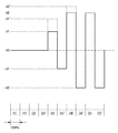
図4乃至図8は、本実施形態に係る表示装置内の各信号処理部における液晶パネルの特定の画素を駆動する信号を示している。 4 to 8 show signals for driving specific pixels of the liquid crystal panel in each signal processing unit in the display device according to the present embodiment.
まず図4は、フレームレート変換部101に入力される液晶パネルの特定の画素を駆動する信号を示す図である。図4では、60Hzの5フレーム分の映像入力信号に対応する。このうち、フレーム(1)及び(2)では、黒信号が印加され(電圧V0)、フレーム(3)にて中間調画像データ1(電圧V1)に変化している。更に、フレーム(4)では中間調画像データ1より明るい中間調画像データ2(電圧V2)に変化している。
First, FIG. 4 is a diagram illustrating a signal for driving a specific pixel of the liquid crystal panel input to the frame
次に、図5は、フレームレート変換部101から出力される画像データを示す図である。この図5では、フレーム(1)はフレーム(1)と(1)’に、フレーム(2)はフレーム(2),(2)'(以下同様)というように、図4に示す各フレームが2つのフレームに分割されて表されている。
Next, FIG. 5 is a diagram illustrating image data output from the frame
本実施形態では、フレームレート変換部101は、画像のフレームレートを60Hzから120Hzに変換している。このフレームレート変換部101では、メモリ33に記憶されている画像データを連続して2回づつ読み出すことによりフレームレートを2倍に変換している。次に、応答速度補正部103は、表示装置200の応答速度を改善するために、駆動電圧を補正して、所謂オーバードライブ駆動を行う。
In the present embodiment, the frame
図6は、本実施形態に係る応答速度補正部103から出力される画像データを示す図である。
FIG. 6 is a diagram showing image data output from the response
応答速度補正部103では、メモリ102に記憶した1フレーム前の画像データと現時点の画像データとを比較し、それら画像データに変化があれば、その結果に応じて、オーバードライブ駆動を行う。図5の例では、フレーム(3)は、1つ前のフレーム(2)'と異なっているため、このフレーム(3)で、電圧V1を電圧V1'に補正してオーバードライブ駆動が実行される。電圧V1'と電圧V1の差分値は、遷移前の電圧V1と遷移後の電圧V0に対応する補正値である。
The response
更に、フレーム(4)は、1つ前のフレーム(3)'と異なっているため、このフレーム(4)で、電圧V2を補正して電圧V2'でオーバードライブ駆動が実行される。この電圧V2'と電圧V2の差分値は、遷移前の電圧V2と遷移後電圧V1に対応する補正値である。続く図5のフレーム(4)'以降では、2フレーム前のフレーム(4)以降と同じデータであるためオーバードライブ駆動は行なわれない。 Further, since the frame (4) is different from the previous frame (3) ′, in this frame (4), the voltage V2 is corrected and overdrive driving is executed with the voltage V2 ′. The difference value between the voltage V2 ′ and the voltage V2 is a correction value corresponding to the voltage V2 before transition and the voltage V1 after transition. In the subsequent frame (4) ′ in FIG. 5, the overdrive drive is not performed because the data is the same as that in the frame (4) after the previous two frames.
このように図6では、入力信号において、黒から中間調1に変化したフレーム(3)及び、中間調1から中間調2に変化したフレーム(4)で、オーバードライブ駆動が行われる。ここで、フレーム(3)とフレーム(4)とでオーバードライブ量(補正量)が異なるのは、遷移前後のレベルが異なるためである。
As described above, in FIG. 6, overdrive driving is performed in the input signal in the frame (3) that has changed from black to
応答速度補正の方法としては、LUTにより1フレーム前の画像データと現時点の表示画像データの入力レベルに応じて補正量を変える方法や、1フレーム前の画像データと現時点の表示画像データとの差分に応じて補正量を決める方法等がある。LUTを使用する方法では、応答速度が遅い中間調での補正量を増やす等、変化レベルに応じた最適なオーバードライブ駆動が可能となる。 As a response speed correction method, a method of changing the correction amount according to the input level of the image data of the previous frame and the current display image data by the LUT, or the difference between the image data of the previous frame and the current display image data. There is a method of determining the correction amount according to the above. In the method using the LUT, it is possible to perform the optimum overdrive drive corresponding to the change level, such as increasing the correction amount in the halftone with a slow response speed.
次に極性反転部106では、2倍に変換された後の1フレーム毎に、信号の極性を反転して出力する。
Next, the
図7は、本実施形態に係る極性反転部106における、図6に示す倍速変換後の信号を、各フレームごとに信号の駆動極性を反転する状態を示す図である。尚、図7における各フレームは、図6に示す各フレームと同一であり、その駆動電圧V1、V2、V1’、V2’も図6と同じである。
FIG. 7 is a diagram illustrating a state in which the polarity of the signal after the double speed conversion illustrated in FIG. 6 is reversed in each frame in the
図7では、倍速変換後のフレームに対して、最初のフレームを正極性で、次のフレームを負極性という様に、隣り合うフレームについて順に極性反転を繰り返す。即ち、フレーム(1)、(2)、(3)、(4)及び(5)は正極性となり、フレーム(1)’、(2)’、(3)’(4)’及び(5)’は負極性となる。よって、オーバードライブを倍速後の最初のフィールドで行うと、オーバードライブが正極性側に偏ってしまうため、液晶に直流成分が残るという問題がある。そのため、所定のタイミングで、極性反転の順序を切替える。つまり、入力の1フレームに対する倍速後の最初のフィールドの極性が負側から始まるようにする。 In FIG. 7, the polarity inversion is repeated in order for adjacent frames such that the first frame is positive and the next frame is negative with respect to the frame after double speed conversion. That is, the frames (1), (2), (3), (4) and (5) are positive and the frames (1) ′, (2) ′, (3) ′ (4) ′ and (5) 'Is negative polarity. Therefore, when overdrive is performed in the first field after the double speed, the overdrive is biased to the positive polarity side, and there is a problem that a direct current component remains in the liquid crystal. Therefore, the polarity inversion order is switched at a predetermined timing. That is, the polarity of the first field after double speed for one frame of input starts from the negative side.
図8に極性反転の順序を切替える例について説明する。図7では、倍速後の最初のフィールド(1)、(2)、(3)では正極性で駆動され、倍速後の2番目のフィールド(1)’、(2)’、(3)は負極性で駆動される。そして、(3)’フレームと(4)フレームの切替時に交流駆動順序切替が指示されると、これまでとは逆に、倍速後の最初のフィールド(4)、(5)は負極性で駆動され、倍速後の2番目のフィールド(4)’、(5)’は正極性で駆動される。これにより、オーバードライブが行われる極性が切り替わるため、直流成分の残余を改善することができる。 An example of switching the order of polarity inversion will be described with reference to FIG. In FIG. 7, the first fields (1), (2), and (3) after double speed are driven with positive polarity, and the second fields (1) ′, (2) ′, and (3) after double speed are negative electrodes. Driven by sex. And, when the AC drive order switching is instructed at the time of switching between the (3) ′ frame and the (4) frame, the first fields (4) and (5) after the double speed are driven with negative polarity. The second fields (4) ′ and (5) ′ after the double speed are driven with positive polarity. Thereby, since the polarity in which overdrive is performed switches, the remainder of a DC component can be improved.
本実施形態では、表示装置200に対する入力信号を切り替えるためにリモコン61が操作され、入力信号の切替が行われるタイミングで、極性反転順序の切替えを行う。そこで、図9を参照して、極性反転順序の切替処理を説明する。図9は、極性反転順序の切替処理の一例を示すフローチャートである。
In the present embodiment, the polarity reversal order is switched at the timing when the remote controller 61 is operated to switch the input signal to the
まず、リモコン61に対して入力切替指示の操作が行われると、ステップS901では、操作に応じてリモコン61から送信される信号を制御パネル62が受信する。制御パネル62は、リモコンからの信号受信をCPU63に通知する。CPU63はこの通知に応じて、ステップS902にて、まずDSP32を制御して表示画面を黒表示とする。表示画面を黒表示にすることにより、入力切替指示を行う際のスイッチ30による切替ノイズを隠すことができる。
First, when an input switching instruction operation is performed on the remote controller 61, in step S901, the
黒画面表示を行っている間に、さらにCPU63はステップS903にて、極性反転制御部131を制御して、極性反転順序変更の指示を極性反転部106に出力させ、極性反転順序を変更させる。さらに、ステップS904では、CPU63はスイッチ30の切替えを指示し、入力をPC入力50またはNTSC入力51に切り替える。さらに、ステップS905においてCPU63は、DSP32による黒表示設定を解除する。
While the black screen is being displayed, the
このようにして、入力切替の黒画面表示時に極性反転順序を切替えることにより、極性反転順序切替え時に同極性が連続することにより発生する表示画面のフリッカーによる画質劣化を改善することができる。 In this way, by switching the polarity inversion order during black screen display of input switching, it is possible to improve image quality degradation due to display screen flicker that occurs when the same polarity continues during polarity inversion order switching.
なお、図9では、リモコン61の入力信号の切替指示の操作に応じて極性反転順序を変更した。しかし、変更のトリガとなるのは、入力信号の切替指示の操作のみに限定されるものではない。これ以外にも、例えば放送番組の切替指示(チャンネル切替指示)のための操作が行われた場合も、該操作に応じて極性反転順序を変更することができる。 In FIG. 9, the polarity inversion order is changed according to the operation of the input signal switching instruction of the remote controller 61. However, the trigger for the change is not limited to the operation of the input signal switching instruction. In addition to this, for example, when an operation for a broadcast program switching instruction (channel switching instruction) is performed, the polarity inversion order can be changed according to the operation.
次に図10を参照して、本実施形態における応答速度の補正処理を説明する。図10は、発明の実施形態に対応する応答速度の補正処理の一例を示すフローチャートである。この処理は、応答速度補正部103、フレームレート変換部101、極性反転部106により実行されるが、ROM64に記憶されたプログラムに基づいてCPU63の制御の下で実行されても良い。
Next, with reference to FIG. 10, the response speed correction processing in this embodiment will be described. FIG. 10 is a flowchart illustrating an example of a response speed correction process corresponding to the embodiment of the invention. This process is executed by the response
まず、ステップS1001では、フレームレート変換部101に、DSP32で処理された現画像データが入力される。次に、ステップS1002では、フレームレート変換部101において、入力された現画像データのフレームレートを2倍に変換する。続くステップS1003では、フレームレートが変換された現画像データと、メモリ33に格納されている1フレーム前の前画像データの値を比較する。
First, in step S1001, the current image data processed by the DSP 32 is input to the frame
もし、両者の値が一致する場合には(ステップS1004において「YES」)、ステップS1006に移行する。一方、両者の値が異なる場合には(ステップS1004において「NO」)、ステップS1005に移行する。ステップS1005では、応答速度補正部103において、オーバードライブ駆動を行うために、1フレーム前の画像と現画像の遷移方向に応じて、現画像データの駆動電圧を上昇または下降させる。すなわち、1フレーム前の画像と現画像の遷移方向が上昇方向であれば、駆動電圧を更に上昇させ、逆に、1フレーム前の画像と現画像の遷移方向が下降方向であれば、駆動電圧を更に下降させる。次に、ステップS1006では、極性反転順序の変更を行うか否かが判定される。この判定は、タイミング検出部132により極性反転順序変更のタイミングが検出され、極性反転制御部131に極性反転順序変更の指示があるか否かに基づいて行う。もし、極性反転順序の変更を行うと判定された場合には(ステップS1006において「YES」)、ステップS1007に移行する。一方、極性反転順序の変更を行う必要がないと判定された場合には(ステップS1006において「NO」)、ステップS1008に移行する。
If the two values match (“YES” in step S1004), the process proceeds to step S1006. On the other hand, if the two values are different (“NO” in step S1004), the process proceeds to step S1005. In step S1005, the response
ステップS1007では、極性反転制御部131にて極性反転順序変更の設定を行い、ステップS1008に移行する。ステップS1008では、極性反転部106により、各フレームごとに信号の極性を反転させてD/A変換器35に出力する。さらに、ステップS1009では、D/A変換器35からの出力信号に基づきR,G,Bの各液晶パネル2R、2G、2Bを表示駆動する。さらにステップS1010では、画像の表示処理を終了するか否かを判定し、終了しない場合は(ステップS1010において「NO」)、ステップS1001に戻って処理を継続する。表示処理を終了する場合は(ステップS1010において「YES」)、そのまま処理を終了する。
In step S1007, the polarity
これにより、正転駆動時と反転駆動時において、同等にオーバードライブが行われる。 As a result, overdrive is performed equally during forward rotation and reverse rotation.
以上説明したように本実施形態によれば、正転駆動時と反転駆動時においてオーバードライブ駆動電圧のバランスがとれるため、表示画像の信頼性が向上する。 As described above, according to the present embodiment, the overdrive drive voltage can be balanced during forward rotation drive and reverse drive, so that the reliability of the display image is improved.
[第2の実施形態]
次に発明の第2の実施形態について説明する。本実施形態では、上述の第1の実施形態に比べて、より多い頻度で極性反転の順序を切替える方法について説明する。
[Second Embodiment]
Next, a second embodiment of the invention will be described. In the present embodiment, a method for switching the order of polarity inversion more frequently than in the first embodiment described above will be described.
図11は、本実施形態に対応する信号処理系の一例を示す構成図である。図11の構成では、図3のフレームレート変換部101以降の構成において、新たにシーンチェンジ検出部1101を含む点に特徴がある。
FIG. 11 is a configuration diagram illustrating an example of a signal processing system corresponding to the present embodiment. The configuration of FIG. 11 is characterized in that a scene
このシーンチェンジ検出部1101では、メモリ102より出力される1フレーム前(直前)の画像の平均輝度値と、フレームレート変換部101より出力される現フレームの画像の平均輝度値とを比較して、シーンチェンジが発生したかを判定する。本実施形態では、平均輝度値の変化の度合い、具体的には平均輝度値が50%変化したか否かを基準に、シーンチェンジが発生したか否かを判定する。
In this scene
シーンチェンジ検出部1101によりシーンチェンジの発生が検出されると、シーンチェンジ検出部1101は、シーンチェンジの発生をタイミング検出部132に通知する。この通知に応じてタイミング検出部132から極性反転制御部131へ、極性を反転させるタイミングが到来したことが通知される。極性反転制御部131は、この通知に応じて極性反転の順序を設定し、極性反転部106がこの設定に応じて極性反転の順序を変更して液晶パネルを駆動する。
When the scene
極性反転の順序を変更した場合、フリッカーの知覚による画質劣化を生ずるおそれがある。しかし、このような画質劣化は、該順序変更をシーンチェンジ時のような画面の輝度変化が大きい状況で行うことで防止することができる。 When the order of polarity inversion is changed, there is a risk of image quality degradation due to flicker perception. However, such image quality deterioration can be prevented by performing the change of order in a situation where the screen luminance change is large as in the case of a scene change.
なお、本実施形態では、平均輝度によりシーンチェンジが発生したか否かを判断したが、これに限らず、輝度の最大値、最小値、色情報、映像に予め埋め込まれたシーン情報を利用することもできる。 In the present embodiment, whether or not a scene change has occurred is determined based on the average luminance. However, the present invention is not limited to this, and the maximum luminance value, the minimum luminance value, color information, and scene information embedded in the video in advance are used. You can also.
このように、本実施形態ではシーンチェンジの発生をトリガとして極性反転の順序を変更する頻度をより多くすることができるので、正転駆動時と反転駆動時においてオーバードライブ駆動電圧のバランスがとれるため信頼性がより向上する。 As described above, in this embodiment, the frequency of changing the order of polarity inversion can be increased by using the occurrence of a scene change as a trigger, so that the overdrive drive voltage can be balanced during forward rotation and reverse rotation. Reliability is further improved.
[第3の実施形態]
次に発明の第3の実施形態について説明する。本実施形態は、投射する光量を制御する絞り機構を備えた投射型表示装置に、前述の極性反転順序の切替を適用した例について説明する。
[Third Embodiment]
Next, a third embodiment of the invention will be described. In the present embodiment, an example in which the above-described switching of the polarity inversion order is applied to a projection type display device having a diaphragm mechanism for controlling the amount of light to be projected will be described.
以下、本実施形態について図面を参照して詳細に説明する。図12は本実施形態に対応する投射型画像表示装置の構成の一例を示す図である。図12において、符号1201は投射型画像表示装置全体を示している。この投射型画像表示装置1201は、光変調素子P、照明装置BL1、投影光学系PL1を備えており、投射光を図示しないスクリーンに投影することによって画像を表示するように構成されている。
Hereinafter, the present embodiment will be described in detail with reference to the drawings. FIG. 12 is a diagram showing an example of the configuration of a projection type image display apparatus corresponding to this embodiment. In FIG. 12,
ここで、光変調素子Pは、光の透過あるいは反射の状態を制御することにより階調画像を表示する素子である。投影光学系PL1は、光変調素子Pに照射された光の透過光あるいは反射光を投影する。照明装置BL1は、光変調素子Pに対して光を照射し、リフレクタ1203と発光管1202とで構成される。照明装置BL1と光変調素子Pとの間には、カラーフィルタ1204、テレセントリックレンズ1205a、1205b、フライアイインテグレータ1206a、1206bが配置されている。フライアイインテグレータ1206a、1206bで積分処理された光は集光反射ミラー1207で光変調素子Pに集光される。
Here, the light modulation element P is an element that displays a gradation image by controlling the transmission or reflection state of light. The projection optical system PL1 projects transmitted light or reflected light of the light irradiated to the light modulation element P. The illumination device BL1 irradiates light to the light modulation element P, and includes a
投射型画像表示装置1201は、書き込み信号処理部1210、投影光量制御部1220、制御信号生成部1230をさらに備えている。ここで、書き込み信号処理部1210は、光変調素子Pへの書き込み信号の変調処理を行う。投影光量制御部1220は、光変調素子Pから透過あるいは反射してきた光量の制御を行う。また、制御信号生成部1230は、書き込み信号処理部1210及び投影光量制御部1220の制御を行う。
The projection type
制御信号生成部1230は、入力画像信号の輝度レベルに基づいて、輝度レベルが高い場合には(即ち輝度レベルが高いほど)投影光量を大きく、且つ、書き込み信号の変調を小さくするように制御信号を生成する。また、輝度レベルが低い場合には(即ち輝度レベルが低いほど)投影光量を小さく、且つ、書き込み信号の変調を大きくするように制御信号を生成する。
Based on the luminance level of the input image signal, the control
本実施形態では、投影光学系PL1を所謂シュリーレン光学系で構成することが好ましい。また、投影光量制御部1220は、可動絞り部1220aと、絞り駆動部1220bとによって構成され、光変調素子Pと共役関係にならない位置に配置されている。投影光量制御部1220は、入力画像信号の輝度レベルに応じて、絞り駆動部1220bによって可動絞り部1220aを開いたり、閉じたりして絞り量を制御する。
In the present embodiment, it is preferable that the projection optical system PL1 is a so-called Schlieren optical system. The projection light
また、制御信号生成部1230は、入力画像信号の輝度レベルを算出する輝度レベル演算部1230a、演算された輝度レベルに応じて投影光学系から出射する投影光量を算出する投影光量演算部1230bによって構成されている。そして、制御信号生成部1230は、投影光量演算部1230bにおいて演算された投影光量に基づいて投影光量制御部1220の制御信号を生成する。また、輝度レベル演算部1230aにおいて演算された輝度レベル及び演算された投影光量に基づいて、書き込み信号処理部1210の制御信号を生成する。
The control
輝度レベル演算部1230aは、入力画像信号の各フィールド又は各フレームにおける各画素の輝度信号の最大値を最大輝度として算出する。この場合、1フィールド又は1フレーム内の入力画像信号を順に比較することにより算出することができる。また、各画素の輝度信号の累積ヒストグラムを演算し、累積ヒストグラムが一定以上となる輝度レベルを最大輝度として算出すると良い。
The luminance
ここで、輝度レベル演算部1230aにより、最大輝度または平均輝度が、所定のレベル以下に設定された場合は、可動絞り部1220aを絞って投射光量を少なくすることにより、黒浮きの少ない、締まった黒表示が可能となる。この時に極性反転の順序を切替えることにより、フリッカーによる表示品位の劣化を起こすことなく、信号の極性反転順序の切替えが可能となる。
Here, when the maximum luminance or the average luminance is set to a predetermined level or less by the luminance
また、可動絞り部1220aの制御量が大きく、光量が大きく変化する場合においても、極性反転の順序の変更によるフリッカーの知覚による画質劣化を防止できるため、極性反転のタイミングとしては好ましい。この場合、制御量について閾値を設定し、該閾値との比較により制御量が閾値を上回る場合に、極性反転の順序を変更するタイミングを決定することができる。
In addition, even when the control amount of the
本実施形態では、光変調素子Pにより反射された光を光量変調部である可動絞りにより光量を制御する方法について説明したが、これに限らず、光量変調素子Pに照射する光量を光量変調部により制御してもよい。また、光量変調部としても絞り以外の例えば光の偏向を利用して光量を制御する部を用いてもよいし、これに限るものではない。 In the present embodiment, the method of controlling the light amount of the light reflected by the light modulation element P using the movable diaphragm that is the light amount modulation unit has been described. It may be controlled by. Further, as the light amount modulation unit, a unit for controlling the light amount by utilizing, for example, light deflection other than the diaphragm may be used, and the present invention is not limited to this.
また、光変調素子としては、LCOS、DMDなどの反射型の素子だけではなく、透過型の液晶パネルにも適用できる。 Further, the light modulation element can be applied not only to a reflection type element such as LCOS or DMD but also to a transmission type liquid crystal panel.
以上説明したように本実施形態によれば、光量の制御状況をトリガとして極性反転の順序を変更する頻度をより多くすることができるので、正転駆動時と反転駆動時においてオーバードライブ駆動電圧のバランスがとれるため信頼性がより向上する。 As described above, according to the present embodiment, the frequency of changing the order of polarity reversal can be increased using the light intensity control status as a trigger. Reliability is further improved due to the balance.
[第4の実施形態]
次に発明の第4の実施形態について説明する。本実施形態では、前述の実施形態に比べて、より間便な方法で極性反転の順序を切替える方法について図3を用いて説明する。
[Fourth Embodiment]
Next, a fourth embodiment of the invention will be described. In the present embodiment, a method for switching the order of polarity inversion in a more convenient method than in the above-described embodiment will be described with reference to FIG.
不図示の電源SWにおいて、電源58がONされ動作用電源の供給が開始されると、CPU63により電源のONを検出し、前回の電源OFF時における極性反転順序情報を不揮発性RAM65より読み出す。そして、不揮発性RAM65より読み出した極性反転情報とは異なる極性反転順序を極性反転制御部131に設定し、極性反転部106により、以前と異なる極性反転順序により表示パネルを駆動する。
When the
不図示の電源SWにおいて、電源58がOFFされ動作用電源の供給が停止された場合は、CPU63により電源のOFFを検出し、電源OFF時における極性反転順序情報を不揮発性RAM64に書き込む。
In the power supply SW (not shown), when the
このように、本実施形態では電源スイッチのON/OFFをトリガとして極性反転の順序を変更する頻度をより多くすることができるので、正転駆動時と反転駆動時においてオーバードライブ駆動電圧のバランスがとれるため信頼性がより向上する。 As described above, in this embodiment, the frequency of changing the order of polarity reversal can be increased by using ON / OFF of the power switch as a trigger, so that the balance of the overdrive drive voltage during forward rotation drive and reverse drive is improved. Therefore, reliability is further improved.
本実施形態では、電源のON時に極性反転順序を変更する例について説明したが、これに限らず電源OFF時に極性反転順序を変更する方法としてもよい。 In the present embodiment, the example in which the polarity inversion order is changed when the power is turned on has been described.
[第5の実施形態]
次に発明の第5の実施形態について説明する。本実施形態では、前述の実施形態に比べて、より間便な方法で極性反転の順序を切替える方法について図3を用いて説明する。
[Fifth Embodiment]
Next, a fifth embodiment of the invention will be described. In the present embodiment, a method for switching the order of polarity inversion in a more convenient method than in the above-described embodiment will be described with reference to FIG.
CPU63のタイマ機能を用いて、所定時間の経過毎に極性反転制御部131により極性反転の順序を変更する。切替時間としては、液晶の特性から、10分から60分程度の間が好ましい。
Using the timer function of the
また、このタイマ機能と前述の実施形態とを組合わせて、所定の時間の到来を検出した場合に、各種の条件を検出するようにしてもよい。即ち、所定の時間が到来した後に、入力切替やチャンネル切替が行われた場合、あるいは、シーンチェンジが発生した場合に、極性反転の順序を変更することができる。これにより、定期的に極性反転の順序を変更することができると共に、変更時の画質劣化を防止することができる。 Further, various conditions may be detected when the arrival of a predetermined time is detected by combining this timer function and the above-described embodiment. That is, the order of polarity inversion can be changed when input switching or channel switching is performed after a predetermined time, or when a scene change occurs. Thereby, the order of polarity inversion can be changed periodically, and image quality deterioration at the time of change can be prevented.
以上説明したように上述の第1乃至第5の実施形態に関わる表示装置によれば、交流電圧駆動を行う液晶表示装置において、所定のタイミングで正転駆動と反転駆動の順序を変更する。これにより、オーバードライブ駆動による直流成分による信号の劣化を改善できる。特に本実施形態の構成によれば、特殊な構造を採用することなく、一般的な表示装置に適応できる。更に、信頼性を低下させずに、高画質な表示装置を提供することが可能となる。 As described above, according to the display devices according to the first to fifth embodiments described above, in the liquid crystal display device that performs AC voltage driving, the order of normal rotation driving and inversion driving is changed at a predetermined timing. Thereby, it is possible to improve signal deterioration due to a direct current component due to overdrive driving. In particular, according to the configuration of the present embodiment, it can be applied to a general display device without adopting a special structure. Furthermore, it is possible to provide a display device with high image quality without reducing reliability.
[その他の実施形態]
なお、本発明は、複数の機器(例えばホストコンピュータ、インタフェイス機器、リーダ、プリンタなど)から構成されるシステムに適用しても、一つの機器からなる装置(例えば、複写機、ファクシミリ装置など)に適用してもよい。
[Other Embodiments]
Note that the present invention can be applied to a system including a plurality of devices (for example, a host computer, an interface device, a reader, and a printer), and a device (for example, a copying machine and a facsimile device) including a single device. You may apply to.
また、本発明の目的は、前述した機能を実現するソフトウェアのプログラムコードを記録した記憶媒体を、システムに供給し、そのシステムがプログラムコードを読み出し実行することによっても達成される。この場合、記憶媒体から読み出されたプログラムコード自体が前述した実施形態の機能を実現し、そのプログラムコードを記憶した記憶媒体は本発明を構成する。また、そのプログラムコードの指示に基づき、コンピュータ上で稼働しているオペレーティングシステム(OS)などが実際の処理の一部または全部を行い、その処理によって前述した機能が実現される場合も含まれる。 The object of the present invention can also be achieved by supplying a storage medium storing software program codes for realizing the above-described functions to the system, and the system reading and executing the program codes. In this case, the program code itself read from the storage medium realizes the functions of the above-described embodiments, and the storage medium storing the program code constitutes the present invention. In addition, an operating system (OS) running on a computer performs part or all of actual processing based on an instruction of the program code, and the above-described functions are realized by the processing.
さらに、以下の形態で実現しても構わない。すなわち、記憶媒体から読み出されたプログラムコードを、コンピュータに挿入された機能拡張カードやコンピュータに接続された機能拡張ユニットに備わるメモリに書込む。そして、そのプログラムコードの指示に基づき、その機能拡張カードや機能拡張ユニットに備わるCPUなどが実際の処理の一部または全部を行って、前述した機能が実現される場合も含まれる。 Furthermore, you may implement | achieve with the following forms. That is, the program code read from the storage medium is written into a memory provided in a function expansion card inserted into the computer or a function expansion unit connected to the computer. Then, based on the instruction of the program code, the case where the above-described functions are realized by the CPU included in the function expansion card or the function expansion unit performing part or all of the actual processing is also included.
本発明を上記記憶媒体に適用する場合、その記憶媒体には、先に説明したフローチャートに対応するプログラムコードが格納されることになる。 When the present invention is applied to the storage medium, the storage medium stores program codes corresponding to the flowcharts described above.
Claims (9)
入力された画像データを1フレーム毎にN分割することによりN倍のフレームレートに変換する変換手段と、
前記変換手段によって変換された画像データにつき、時間的に前後する画像データの差分に基づいて前記液晶表示手段を駆動するための駆動電圧を補正する補正手段と、
前記補正手段により補正された画像データを含む前記画像データにつき、時間的に前後する画像データの駆動極性が異なるように極性を反転させる反転手段と、
前記極性が反転された画像データを用いて前記液晶表示手段を駆動する駆動手段と、
前記極性を反転させる順序を切り替える制御手段と、
前記画像データの入力を行うための、少なくとも2以上の入力手段と、
前記2以上の入力手段を切り替えて、いずれか1つより前記画像データの入力を行わせるための入力切替手段と、
前記入力切替手段に対する切替指示を受け付ける受付手段と、
を備え、
前記受付手段により前記切替指示を受け付けた場合に、前記制御手段は、前記極性を反転させる順序を切り替える
ことを特徴とする液晶表示装置。 Liquid crystal display means driven by alternating voltage;
Conversion means for converting the input image data into N frame rates by dividing the input image data into N frames for each frame;
Correction means for correcting the drive voltage for driving the liquid crystal display means based on the difference between the image data temporally changing with respect to the image data converted by the conversion means,
Reversing means for reversing the polarity of the image data including the image data corrected by the correcting means so that the driving polarity of the image data before and after is different;
Drive means for driving the liquid crystal display means using the image data with the polarity reversed;
Control means for switching the order of reversing the polarity;
At least two or more input means for inputting the image data;
An input switching means for switching the two or more input means to input the image data from any one of them;
Receiving means for receiving a switching instruction for the input switching means;
With
When the switching instruction is received by the receiving means, the control means switches the order of inverting the polarity.
前記受付手段は、前記チャンネルの切替指示をさらに受け付け、
前記受付手段により前記チャンネルの切替指示を受け付けた場合に、前記制御手段は、前記極性を反転させる順序を切り替える
ことを特徴とする請求項1に記載の液晶表示装置。 When image data of a program broadcast using a plurality of channels is input by any one of the two or more input means,
The accepting means further accepts an instruction to switch the channel;
2. The liquid crystal display device according to claim 1, wherein when the channel switching instruction is received by the receiving unit, the control unit switches the order of inverting the polarity.
前記液晶表示手段は前記駆動手段により黒表示となるように駆動される
ことを特徴とする請求項1または2に記載の液晶表示装置。 When switching of the order of inverting the polarity is performed by the control means,
The liquid crystal display device according to claim 1, wherein the liquid crystal display unit is driven by the driving unit so as to display black.
入力された画像データを1フレーム毎にN分割することによりN倍のフレームレートに変換する変換手段と、
前記変換手段によって変換された画像データにつき、時間的に前後する画像データの差分に基づいて前記液晶表示手段を駆動するための駆動電圧を補正する補正手段と、
前記補正手段により補正された画像データを含む前記画像データにつき、時間的に前後する画像データの駆動極性が異なるように極性を反転させる反転手段と、
前記極性が反転された画像データを用いて前記液晶表示手段を駆動する駆動手段と、
前記極性を反転させる順序を切り替える制御手段と、
前記液晶表示手段を介して液晶表示装置の外部に投射される光量と、前記液晶表示手段に投射される光量との少なくともいずれかを制御する光量制御手段と
を備え、
前記光量制御手段により制御された前記光量が予め定められた光量を下回る場合と、前記光量制御手段による前記光量の制御量が予め定められた制御量を上回る場合との少なくともいずれかにおいて、前記制御手段により前記極性を反転させる順序が切り替えられる
ことを特徴とする液晶表示装置。 Liquid crystal display means driven by alternating voltage;
Conversion means for converting the input image data into N frame rates by dividing the input image data into N frames for each frame;
Correction means for correcting the drive voltage for driving the liquid crystal display means based on the difference between the image data temporally changing with respect to the image data converted by the conversion means,
Reversing means for reversing the polarity of the image data including the image data corrected by the correcting means so that the driving polarity of the image data before and after is different;
Drive means for driving the liquid crystal display means using the image data with the polarity reversed;
Control means for switching the order of reversing the polarity;
A light amount control means for controlling at least one of a light amount projected to the outside of the liquid crystal display device via the liquid crystal display means and a light amount projected to the liquid crystal display means,
The control in at least one of the case where the light amount controlled by the light amount control unit is less than a predetermined light amount and the case where the control amount of the light amount by the light amount control unit exceeds a predetermined control amount. A liquid crystal display device characterized in that the order of inverting the polarity is switched by means.
補正手段が、前記変換された画像データにつき、時間的に前後する画像データの差分に基づいて液晶表示手段を駆動するための駆動電圧を補正する補正工程と、
反転手段が、前記補正工程において補正された画像データを含む前記画像データにつき、時間的に前後する画像データの駆動極性が異なるように極性を反転させる反転工程と、
駆動手段が、前記極性が反転された画像データを用いて前記液晶表示手段を駆動する駆動工程と、
制御手段が、前記極性を反転させる順序を切り替える制御工程と、
少なくとも2以上の入力手段が、前記画像データの入力を行う入力工程と、
入力切替手段が、前記2以上の入力手段を切り替えて、いずれか1つより前記画像データの入力を行わせるための入力切替工程と、
受付手段が、前記入力切替手段に対する切替指示を受け付ける受付工程と、
を備え、
前記受付手段により前記切替指示を受け付けた場合に、前記制御手段は、前記極性を反転させる順序を切り替える
ことを特徴とする液晶表示装置の制御方法。 A conversion step in which the conversion means converts the input image data into N frame rates by dividing the input image data into N frames for each frame;
A correcting step of correcting a driving voltage for driving the liquid crystal display unit based on a difference between temporally changing image data for the converted image data;
An inversion step in which the inversion means inverts the polarity so that the drive polarity of the image data before and after is different for the image data including the image data corrected in the correction step,
A driving step of driving the liquid crystal display means using the image data with the polarity reversed;
A control step of switching the order in which the control means reverses the polarity;
An input step in which at least two or more input means input the image data;
An input switching step for causing the input switching means to switch the two or more input means and to input the image data from any one of them;
A receiving step for receiving a switching instruction to the input switching unit;
With
A control method for a liquid crystal display device, wherein when the switching instruction is received by the receiving means, the control means switches the order of inverting the polarity.
補正手段が、前記変換された画像データにつき、時間的に前後する画像データの差分に基づいて液晶表示手段を駆動するための駆動電圧を補正する補正工程と、
反転手段が、前記補正工程において補正された画像データを含む前記画像データにつき、時間的に前後する画像データの駆動極性が異なるように極性を反転させる反転工程と、
駆動手段が、前記極性が反転された画像データを用いて前記液晶表示手段を駆動する駆動工程と、
制御手段が、前記極性を反転させる順序を切り替える制御工程と、
光量制御手段が、前記液晶表示手段を介して液晶表示装置の外部に投射される光量と、前記液晶表示手段に投射される光量との少なくともいずれかを制御する光量制御工程とを備え、
前記光量制御工程において制御された前記光量が予め定められた光量を下回る場合と、前記光量制御工程における前記光量の制御量が予め定められた制御量を上回る場合との少なくともいずれかにおいて、前記制御工程における前記極性を反転させる順序が切り替えられる
ことを特徴とする液晶表示装置の制御方法。 A conversion step in which the conversion means converts the input image data into N frame rates by dividing the input image data into N frames for each frame;
A correcting step of correcting a driving voltage for driving the liquid crystal display unit based on a difference between temporally changing image data for the converted image data;
An inversion step in which the inversion means inverts the polarity so that the drive polarity of the image data before and after is different for the image data including the image data corrected in the correction step,
A driving step of driving the liquid crystal display means using the image data with the polarity reversed;
A control step of switching the order in which the control means reverses the polarity;
A light amount control unit comprising a light amount control step for controlling at least one of a light amount projected outside the liquid crystal display device via the liquid crystal display unit and a light amount projected onto the liquid crystal display unit;
The control in at least one of the case where the light amount controlled in the light amount control step is lower than a predetermined light amount and the case where the control amount of the light amount in the light amount control step is higher than a predetermined control amount. A method of controlling a liquid crystal display device, wherein the order of reversing the polarity in the process is switched.
画像データの入力を行うための、少なくとも2以上の入力手段と、At least two or more input means for inputting image data;
前記2以上の入力手段を切り替えて、いずれか1つより前記画像データの入力を行わせるための入力切替手段と、An input switching means for switching the two or more input means to input the image data from any one of them;
前記入力切替手段に対する切替指示を受け付ける受付手段とReceiving means for receiving a switching instruction to the input switching means;
を備える液晶表示装置に、In a liquid crystal display device comprising
入力された画像データを1フレーム毎にN分割することによりN倍のフレームレートに変換する変換工程、A conversion step of converting the input image data into N times the frame rate by dividing it into N frames per frame;
前記変換工程において変換された画像データにつき、時間的に前後する画像データの差分に基づいて前記液晶表示手段を駆動するための駆動電圧を補正する補正工程、A correction step for correcting a driving voltage for driving the liquid crystal display means based on a difference between image data temporally changing with respect to the image data converted in the conversion step,
前記補正工程において補正された画像データを含む前記画像データにつき、時間的に前後する画像データの駆動極性が異なるように極性を反転させる反転工程、An inversion step of inverting the polarity of the image data including the image data corrected in the correction step so that the driving polarity of the image data before and after is different.
前記極性が反転された画像データを用いて前記液晶表示手段を駆動する駆動工程、A driving step of driving the liquid crystal display means using the image data with the polarity reversed;
前記受付手段により前記切替指示を受け付けた場合に、前記極性を反転させる順序を切り替える工程、A step of switching the order of inverting the polarity when the switching instruction is received by the receiving means;
を実行させるためのコンピュータプログラム。A computer program for running.
入力された画像データを1フレーム毎にN分割することによりN倍のフレームレートに変換する変換工程、A conversion step of converting the input image data into N times the frame rate by dividing it into N frames per frame;
前記変換工程において変換された画像データにつき、時間的に前後する画像データの差分に基づいて前記液晶表示手段を駆動するための駆動電圧を補正する補正工程、A correction step for correcting a driving voltage for driving the liquid crystal display means based on a difference between image data temporally changing with respect to the image data converted in the conversion step,
前記補正工程において補正された画像データを含む前記画像データにつき、時間的に前後する画像データの駆動極性が異なるように極性を反転させる反転工程、An inversion step of inverting the polarity of the image data including the image data corrected in the correction step so that the driving polarity of the image data before and after is different.
前記極性が反転された画像データを用いて前記液晶表示手段を駆動する駆動工程、A driving step of driving the liquid crystal display means using the image data with the polarity reversed;
前記液晶表示手段を介して液晶表示装置の外部に投射される光量と、前記液晶表示手段に投射される光量との少なくともいずれかを制御する光量制御工程、A light amount control step of controlling at least one of a light amount projected outside the liquid crystal display device via the liquid crystal display means and a light amount projected onto the liquid crystal display means;
前記光量制御工程において制御された前記光量が予め定められた光量を下回る場合と、前記光量制御工程における前記光量の制御量が予め定められた制御量を上回る場合との少なくともいずれかにおいて、前記極性を反転させる順序を切り替える制御工程、The polarity in at least one of the case where the light amount controlled in the light amount control step is lower than a predetermined light amount and the case where the control amount of the light amount in the light amount control step is higher than a predetermined control amount. Control process for switching the order of reversing
を実行させるためのコンピュータプログラム。A computer program for running.
Priority Applications (2)
| Application Number | Priority Date | Filing Date | Title |
|---|---|---|---|
| JP2006325925A JP5110862B2 (en) | 2006-12-01 | 2006-12-01 | Liquid crystal display device and control method thereof, computer program, and storage medium |
| US11/947,171 US8044909B2 (en) | 2006-12-01 | 2007-11-29 | Liquid-crystal display apparatus, control method thereof, and computer program |
Applications Claiming Priority (1)
| Application Number | Priority Date | Filing Date | Title |
|---|---|---|---|
| JP2006325925A JP5110862B2 (en) | 2006-12-01 | 2006-12-01 | Liquid crystal display device and control method thereof, computer program, and storage medium |
Publications (3)
| Publication Number | Publication Date |
|---|---|
| JP2008139580A JP2008139580A (en) | 2008-06-19 |
| JP2008139580A5 JP2008139580A5 (en) | 2010-01-21 |
| JP5110862B2 true JP5110862B2 (en) | 2012-12-26 |
Family
ID=39601112
Family Applications (1)
| Application Number | Title | Priority Date | Filing Date |
|---|---|---|---|
| JP2006325925A Expired - Fee Related JP5110862B2 (en) | 2006-12-01 | 2006-12-01 | Liquid crystal display device and control method thereof, computer program, and storage medium |
Country Status (2)
| Country | Link |
|---|---|
| US (1) | US8044909B2 (en) |
| JP (1) | JP5110862B2 (en) |
Families Citing this family (12)
| Publication number | Priority date | Publication date | Assignee | Title |
|---|---|---|---|---|
| JP4587173B2 (en) * | 2005-04-18 | 2010-11-24 | キヤノン株式会社 | Image display device, control method therefor, program, and recording medium |
| JP5072424B2 (en) * | 2007-05-02 | 2012-11-14 | キヤノン株式会社 | Liquid crystal display |
| JP5060200B2 (en) * | 2007-08-08 | 2012-10-31 | キヤノン株式会社 | Image processing apparatus and image processing method |
| JP5215733B2 (en) * | 2008-05-28 | 2013-06-19 | キヤノン株式会社 | Display control apparatus and overdrive drive parameter determination method |
| JP5264348B2 (en) * | 2008-07-29 | 2013-08-14 | キヤノン株式会社 | Image processing apparatus, control method therefor, computer program, and storage medium |
| JPWO2011065061A1 (en) * | 2009-11-24 | 2013-04-11 | シャープ株式会社 | Liquid crystal display device, polarity inversion method, program, and recording medium |
| JP5797557B2 (en) * | 2009-11-27 | 2015-10-21 | シャープ株式会社 | Liquid crystal display device, television receiver |
| KR101319354B1 (en) * | 2009-12-21 | 2013-10-16 | 엘지디스플레이 주식회사 | Liquid crystal display device and video processing method thereof |
| TWI459355B (en) * | 2012-03-22 | 2014-11-01 | Chunghwa Picture Tubes Ltd | Liquid crystal display |
| JP6290576B2 (en) * | 2012-10-12 | 2018-03-07 | 株式会社半導体エネルギー研究所 | Liquid crystal display device and driving method thereof |
| JP6249688B2 (en) * | 2012-10-16 | 2017-12-20 | キヤノン株式会社 | Display device, display method, and program |
| US10224055B2 (en) * | 2015-02-10 | 2019-03-05 | Sony Semiconductor Solutions Corporation | Image processing apparatus, image pickup device, image processing method, and program |
Family Cites Families (20)
| Publication number | Priority date | Publication date | Assignee | Title |
|---|---|---|---|---|
| JP3103146B2 (en) * | 1991-07-31 | 2000-10-23 | 株式会社東芝 | Liquid crystal display |
| JP3305240B2 (en) * | 1997-10-23 | 2002-07-22 | キヤノン株式会社 | Liquid crystal display panel driving device and driving method |
| JP3359270B2 (en) * | 1997-10-24 | 2002-12-24 | キヤノン株式会社 | Memory controller and liquid crystal display |
| JP3517568B2 (en) * | 1997-10-24 | 2004-04-12 | キヤノン株式会社 | Image processing device |
| JP3403032B2 (en) * | 1997-10-24 | 2003-05-06 | キヤノン株式会社 | Driving device and driving method for liquid crystal display panel |
| JP3315632B2 (en) * | 1997-11-06 | 2002-08-19 | キヤノン株式会社 | Memory control device and liquid crystal display device using the same |
| JP3407698B2 (en) | 1999-07-22 | 2003-05-19 | 株式会社日立製作所 | Liquid crystal display |
| JP3713208B2 (en) * | 2000-03-29 | 2005-11-09 | シャープ株式会社 | Liquid crystal display device |
| JP4869524B2 (en) * | 2001-01-30 | 2012-02-08 | 株式会社半導体エネルギー研究所 | Liquid crystal display |
| JP4267873B2 (en) * | 2002-07-11 | 2009-05-27 | パナソニック株式会社 | Image display device and image display method |
| EP1467346B1 (en) * | 2003-04-07 | 2012-03-07 | Samsung Electronics Co., Ltd. | Liquid crystal display and driving method thereof |
| TW594662B (en) * | 2003-06-03 | 2004-06-21 | Chunghwa Picture Tubes Ltd | Method for restraining noise when flat display turn on/off |
| JP2005148606A (en) * | 2003-11-19 | 2005-06-09 | Hitachi Displays Ltd | Method for driving liquid crystal display device |
| JP4564767B2 (en) * | 2004-03-22 | 2010-10-20 | キヤノン株式会社 | Display device, control method therefor, and control program |
| JP4599897B2 (en) * | 2004-06-10 | 2010-12-15 | ソニー株式会社 | Apparatus and method for driving display optical device |
| JP5127121B2 (en) * | 2004-09-14 | 2013-01-23 | キヤノン株式会社 | Display device and display method |
| US7617513B2 (en) * | 2005-01-04 | 2009-11-10 | Avocent Huntsville Corporation | Wireless streaming media systems, devices and methods |
| JP4290140B2 (en) * | 2005-04-04 | 2009-07-01 | キヤノン株式会社 | Display device and display control method thereof |
| US7656374B2 (en) * | 2006-09-04 | 2010-02-02 | Vastview Technology, Inc. | Method for enhancing response speed of hold-typed display device |
| TWI357046B (en) * | 2006-10-24 | 2012-01-21 | Novatek Microelectronics Corp | Method for driving lcd monitors |
-
2006
- 2006-12-01 JP JP2006325925A patent/JP5110862B2/en not_active Expired - Fee Related
-
2007
- 2007-11-29 US US11/947,171 patent/US8044909B2/en not_active Expired - Fee Related
Also Published As
| Publication number | Publication date |
|---|---|
| JP2008139580A (en) | 2008-06-19 |
| US20080252583A1 (en) | 2008-10-16 |
| US8044909B2 (en) | 2011-10-25 |
Similar Documents
| Publication | Publication Date | Title |
|---|---|---|
| JP5110862B2 (en) | Liquid crystal display device and control method thereof, computer program, and storage medium | |
| JP5264348B2 (en) | Image processing apparatus, control method therefor, computer program, and storage medium | |
| JP4290140B2 (en) | Display device and display control method thereof | |
| JP3954979B2 (en) | Projection-type image display device, light deflection device in projection-type image display device, and direct-view-type image display device | |
| TWI402812B (en) | Driving cricuit and gray insertion method of liquid crystal display | |
| JP2006221148A (en) | Image display apparatus and its control method | |
| US8944611B2 (en) | Projector, projector control method, and projection system | |
| EP1988539B1 (en) | Liquid crystal display apparatus | |
| US20070064204A1 (en) | Image display apparatus, and projection system | |
| US8174624B2 (en) | Image processing apparatus and image processing method | |
| JP2009128504A (en) | Liquid crystal display device | |
| JP2008046551A (en) | Display apparatus and method, and program and storage medium | |
| JP2007011393A (en) | Projection-type video display device | |
| JP2005218009A (en) | Image displaying device | |
| JP2009210765A (en) | Projector | |
| JP7267713B2 (en) | PROJECTION DEVICE, CONTROL METHOD THEREOF, AND PROGRAM | |
| JP2005010237A (en) | Projector | |
| JP2008089878A (en) | Projection type video display device | |
| JP2006284825A (en) | Display control circuit for liquid crystal display panel | |
| JP2014219556A (en) | Image display device, image display method, and program | |
| JP5566165B2 (en) | Liquid crystal display | |
| JP2020046598A (en) | Liquid crystal display device | |
| JP2020046474A (en) | Projection control device and method, projection device | |
| JP2021056266A (en) | Display device and driving method of display device | |
| JP2020118780A (en) | Image display device |
Legal Events
| Date | Code | Title | Description |
|---|---|---|---|
| A521 | Request for written amendment filed |
Free format text: JAPANESE INTERMEDIATE CODE: A523 Effective date: 20091130 |
|
| A621 | Written request for application examination |
Free format text: JAPANESE INTERMEDIATE CODE: A621 Effective date: 20091130 |
|
| A131 | Notification of reasons for refusal |
Free format text: JAPANESE INTERMEDIATE CODE: A131 Effective date: 20120127 |
|
| A521 | Request for written amendment filed |
Free format text: JAPANESE INTERMEDIATE CODE: A523 Effective date: 20120326 |
|
| A131 | Notification of reasons for refusal |
Free format text: JAPANESE INTERMEDIATE CODE: A131 Effective date: 20120420 |
|
| A521 | Request for written amendment filed |
Free format text: JAPANESE INTERMEDIATE CODE: A523 Effective date: 20120614 |
|
| A131 | Notification of reasons for refusal |
Free format text: JAPANESE INTERMEDIATE CODE: A131 Effective date: 20120706 |
|
| A521 | Request for written amendment filed |
Free format text: JAPANESE INTERMEDIATE CODE: A523 Effective date: 20120903 |
|
| TRDD | Decision of grant or rejection written | ||
| A01 | Written decision to grant a patent or to grant a registration (utility model) |
Free format text: JAPANESE INTERMEDIATE CODE: A01 Effective date: 20121005 |
|
| A01 | Written decision to grant a patent or to grant a registration (utility model) |
Free format text: JAPANESE INTERMEDIATE CODE: A01 |
|
| A61 | First payment of annual fees (during grant procedure) |
Free format text: JAPANESE INTERMEDIATE CODE: A61 Effective date: 20121009 |
|
| FPAY | Renewal fee payment (event date is renewal date of database) |
Free format text: PAYMENT UNTIL: 20151019 Year of fee payment: 3 |
|
| R151 | Written notification of patent or utility model registration |
Ref document number: 5110862 Country of ref document: JP Free format text: JAPANESE INTERMEDIATE CODE: R151 |
|
| FPAY | Renewal fee payment (event date is renewal date of database) |
Free format text: PAYMENT UNTIL: 20151019 Year of fee payment: 3 |
|
| LAPS | Cancellation because of no payment of annual fees |